


Languages
Pages
Legal

This is information on a product in full production.
May 2016 DocID022644 Rev 2 1/33
ST7580
FSK, PSK multi-mode power line networking system-on-chip
Datasheet - production data
Features
Fully integrated narrow-band power line networking system-on-chip
High-performing PHY processor with embedded turnkey firmware featuring:
– B-FSK modulation up to 9.6 kbps
– B-PSK, Q-PSK, 8-PSK modulations up to 28.8 kbps
– Dual channel operation mode
– Convolutional error correction coding
– Signal-to-noise ratio estimation
– B-PSK with PNA mode against impulsive noise
Protocol engine embedding turnkey communication protocol
– Framing service
– Error detection
– Sniffer functionality
Host controller UART interface up to 57.6 kbps
AES-128 based authentication and confidentiality services
Fully integrated analog front-end:
– ADC and DAC
– Digital transmission level control
– PGA with automatic gain control
– High sensitivity receiver
Fully integrated single-ended power amplifier for line driving
– Up to 1 A RMS, 14 V p-p output
– Configurable active filtering topology
– Very high linearity
– Embedded temperature sensor
– Current control feature
8 to 18 V power amplifier supply
3.3 V or 5 V digital I/O supply
Zero crossing detection
Suitable for EN50065, FCC part 15 and ARIB compliant applications
Communication carrier frequency programmable up to 250 kHz
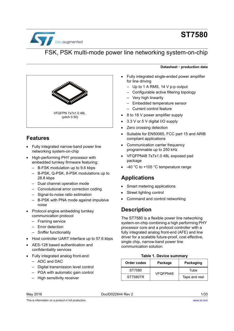
VFQFPN48 7x7x1.0 48L exposed pad package
-40 °C to +105 °C temperature range
Applications
Smart metering applications
Street lighting control
Command and control networking
Description
The ST7580 is a flexible power line networking system-on-chip combining a high performing PHY processor core and a protocol controller with a fully integrated analog front-end (AFE) and line driver for a scalable future-proof, cost effective, single chip, narrow-band power line communication solution.
Table 1. Device summary
Order codes Package Packaging
ST7580VFQFPN48
Tube
ST7580TR Tape and reel
www.st.com
Contents ST7580
2/33 DocID022644 Rev 2
Contents
1 Device overview . . . . . . . . . . . . . . . . . . . . . . . . . . . . . . . . . . . . . . . . . . . . 4
2 Pin connection . . . . . . . . . . . . . . . . . . . . . . . . . . . . . . . . . . . . . . . . . . . . . . 5
Pin description . . . . . . . . . . . . . . . . . . . . . . . . . . . . . . . . . . . . . . . . . . . . . . . . . . . . 6
3 Maximum ratings . . . . . . . . . . . . . . . . . . . . . . . . . . . . . . . . . . . . . . . . . . . . 8
3.1 Absolute maximum ratings . . . . . . . . . . . . . . . . . . . . . . . . . . . . . . . . . . . . . 8
3.2 Thermal data . . . . . . . . . . . . . . . . . . . . . . . . . . . . . . . . . . . . . . . . . . . . . . . 8
4 Electrical characteristics . . . . . . . . . . . . . . . . . . . . . . . . . . . . . . . . . . . . . 9
5 Analog front-end (AFE) . . . . . . . . . . . . . . . . . . . . . . . . . . . . . . . . . . . . . . 15
5.1 Reception path . . . . . . . . . . . . . . . . . . . . . . . . . . . . . . . . . . . . . . . . . . . . . 15
5.2 Transmission path . . . . . . . . . . . . . . . . . . . . . . . . . . . . . . . . . . . . . . . . . . 16
5.3 Power amplifier . . . . . . . . . . . . . . . . . . . . . . . . . . . . . . . . . . . . . . . . . . . . . 16
5.4 Current and voltage control . . . . . . . . . . . . . . . . . . . . . . . . . . . . . . . . . . . 17
5.5 Thermal shutdown and temperature control . . . . . . . . . . . . . . . . . . . . . . . 18
5.6 Zero crossing comparator . . . . . . . . . . . . . . . . . . . . . . . . . . . . . . . . . . . . 18
6 Power management . . . . . . . . . . . . . . . . . . . . . . . . . . . . . . . . . . . . . . . . 19
Ground connections . . . . . . . . . . . . . . . . . . . . . . . . . . . . . . . . . . . . . . . . . . . . . . . 20
7 Clock management . . . . . . . . . . . . . . . . . . . . . . . . . . . . . . . . . . . . . . . . . 22
8 Functional overview . . . . . . . . . . . . . . . . . . . . . . . . . . . . . . . . . . . . . . . . 22
References . . . . . . . . . . . . . . . . . . . . . . . . . . . . . . . . . . . . . . . . . . . . . . . . . . . . . . 23
9 Physical layer . . . . . . . . . . . . . . . . . . . . . . . . . . . . . . . . . . . . . . . . . . . . . 24
9.1 PSK modulations . . . . . . . . . . . . . . . . . . . . . . . . . . . . . . . . . . . . . . . . . . . 24
9.1.1 PSK modes . . . . . . . . . . . . . . . . . . . . . . . . . . . . . . . . . . . . . . . . . . . . . . 24
9.1.2 PSK physical frame . . . . . . . . . . . . . . . . . . . . . . . . . . . . . . . . . . . . . . . . 25
DocID022644 Rev 2 3/33
ST7580 Contents
33
9.2 FSK modulations . . . . . . . . . . . . . . . . . . . . . . . . . . . . . . . . . . . . . . . . . . . 25
9.2.1 FSK options . . . . . . . . . . . . . . . . . . . . . . . . . . . . . . . . . . . . . . . . . . . . . . 25
9.2.2 FSK physical frame . . . . . . . . . . . . . . . . . . . . . . . . . . . . . . . . . . . . . . . . 27
9.2.3 FSK settings . . . . . . . . . . . . . . . . . . . . . . . . . . . . . . . . . . . . . . . . . . . . . 27
9.3 Channel and modulation selection . . . . . . . . . . . . . . . . . . . . . . . . . . . . . . 27
10 Data link layer . . . . . . . . . . . . . . . . . . . . . . . . . . . . . . . . . . . . . . . . . . . . . 29
10.1 Data link frame . . . . . . . . . . . . . . . . . . . . . . . . . . . . . . . . . . . . . . . . . . . . . 29
10.2 Error detection and sniffer mode . . . . . . . . . . . . . . . . . . . . . . . . . . . . . . . 29
10.3 Security services . . . . . . . . . . . . . . . . . . . . . . . . . . . . . . . . . . . . . . . . . . . 29
11 Package information . . . . . . . . . . . . . . . . . . . . . . . . . . . . . . . . . . . . . . . . 30
11.1 VFQFPN48 (7 x 7 x 1.0 mm) package information . . . . . . . . . . . . . . . . . 30
12 Revision history . . . . . . . . . . . . . . . . . . . . . . . . . . . . . . . . . . . . . . . . . . . 32

Device overview ST7580
4/33 DocID022644 Rev 2
1 Device overview
Made using multi-power technology with state-of-the-art VLSI CMOS lithography, the ST7580 is based on dual digital core architecture (a PHY processor engine and a protocol controller core) to guarantee outstanding communication performance with a high level of flexibility for either open standards or customized implementations.
A HW 128-bit AES encryption block with customizable key management is available on chip when secure communication is requested.
The on-chip analog front-end featuring analog to digital and digital to analog conversion, automatic gain control, plus the integrated power amplifier delivering up to 1 A RMS output current makes the ST7580 a unique system-on-chip for power line communication.
Line coupling network design is also simplified, leading to a very low cost BOM.
Robust and performing operations are guaranteed while keeping power consumption and signal distortion levels very low; this makes the ST7580 an ideal platform for the most stringent application requirements and regulatory standards compliance.
Figure 1. Block diagram
AM02502v1
WATCHDOG
TIMERS
Power Management
ADCPGA
DAC GAINCTRL
DDS
Zero CrossingDetection
Line Driver
ThermalManagement
Clock Management
Protocol ControllerTX AFE
PHY processor
BPF
BPF
Output CurrentControl
SPI0/UART
ADC
-+
RX AFE
TX_OUT
RX_IN
PA_OUT
PA_IN-PA_IN+
VCC(8-18V)
CL
VDD(1.8V)
ZC_INVDD_PLL
(1.8V)XIN
VCCA(5V)
T_REQRXD
TXD
BR0
BR1
VDDIO(5 / 3.3V)
ON-CHIP Memories
ON-CHIP Memories
128bit AES
PL_RX_ON
PL_TX_ON
XOUT
DocID022644 Rev 2 5/33
ST7580 Pin connection
33
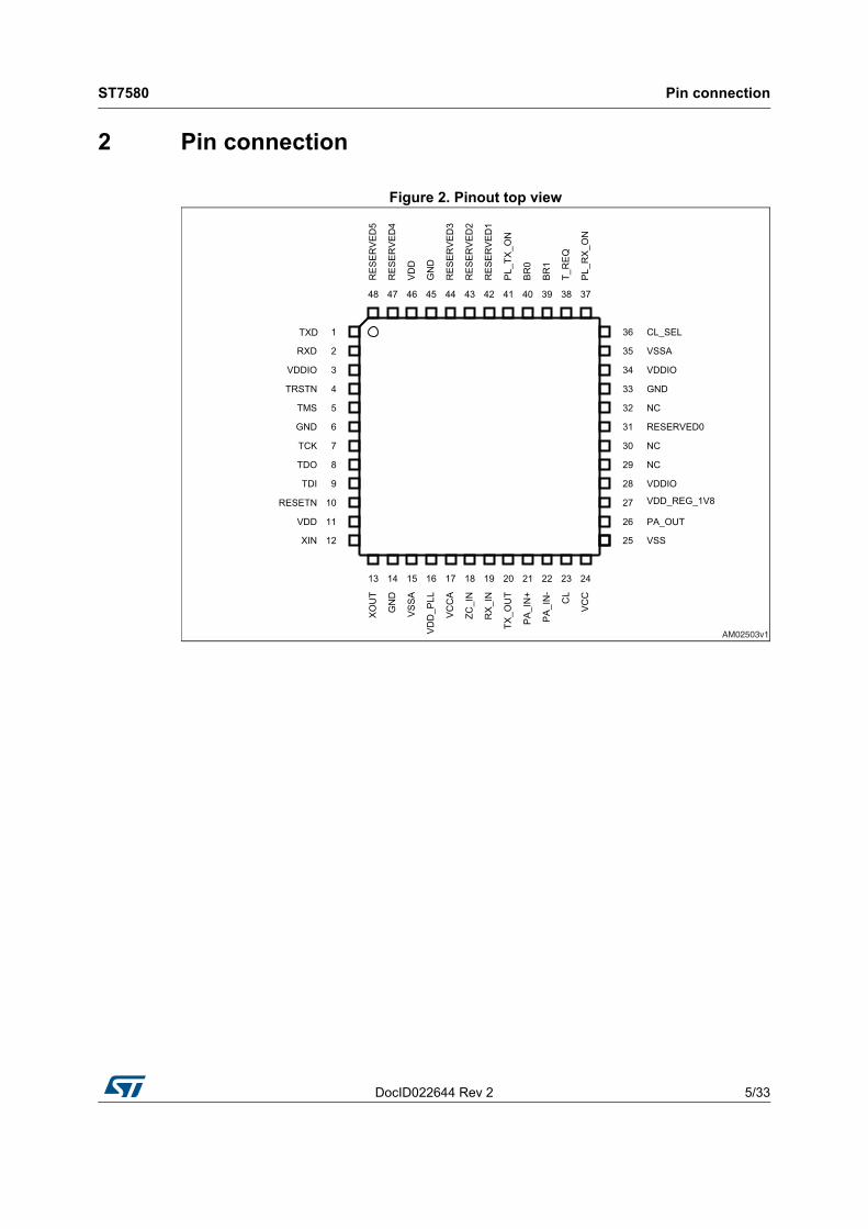
2 Pin connection
Figure 2. Pinout top view
AM02503v1
1
2
3
4
5
6
7
8
9
10
11
12
36
35
34
33
32
31
30
29
28
27
26
25
48 47 46 45 44 43 42 41 40 39 38 37
13 14 15 16 17 18 19 20 21 22 23 24
TXD
VDDIO
TRSTN
TMS
TCK
TDO
TDI
RESETN
VDD
XIN
CL_SEL
VSSA
VDDIO
GND
NC
RESERVED0
NC
NC
VDDIO
VDD_REG_1V8
PA_OUT
VSS
RE
SE
RV
ED
5
RE
SE
RV
ED
4
VD
D
GN
D
RE
SE
RV
ED
3
RE
SE
RV
ED
2
RE
SE
RV
ED
1
PL_
TX_O
N
BR
0
BR
1
T_R
EQ
PL_R
X_O
N
XO
UT
GN
D
VS
SA
VD
D_P
LL
VC
CA
ZC_I
N
RX
_IN
TX_O
UT
PA
_IN
+
PA
_IN
-
CL
VC
C
GND
RXD
Pin connection ST7580
6/33 DocID022644 Rev 2
Pin description
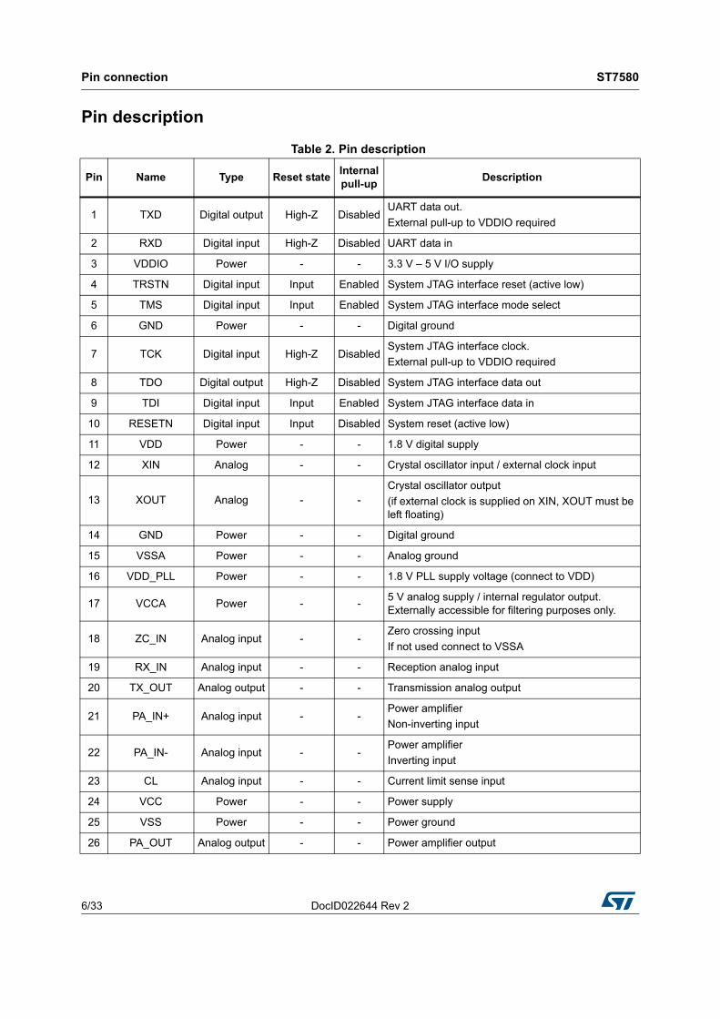
Table 2. Pin description
Pin Name Type Reset stateInternalpull-up
Description
1 TXD Digital output High-Z DisabledUART data out.
External pull-up to VDDIO required
2 RXD Digital input High-Z Disabled UART data in
3 VDDIO Power - - 3.3 V – 5 V I/O supply
4 TRSTN Digital input Input Enabled System JTAG interface reset (active low)
5 TMS Digital input Input Enabled System JTAG interface mode select
6 GND Power - - Digital ground
7 TCK Digital input High-Z DisabledSystem JTAG interface clock.
External pull-up to VDDIO required
8 TDO Digital output High-Z Disabled System JTAG interface data out
9 TDI Digital input Input Enabled System JTAG interface data in
10 RESETN Digital input Input Disabled System reset (active low)
11 VDD Power - - 1.8 V digital supply
12 XIN Analog - - Crystal oscillator input / external clock input
13 XOUT Analog - -Crystal oscillator output
(if external clock is supplied on XIN, XOUT must be left floating)
14 GND Power - - Digital ground
15 VSSA Power - - Analog ground
16 VDD_PLL Power - - 1.8 V PLL supply voltage (connect to VDD)
17 VCCA Power - -5 V analog supply / internal regulator output. Externally accessible for filtering purposes only.
18 ZC_IN Analog input - -Zero crossing input
If not used connect to VSSA
19 RX_IN Analog input - - Reception analog input
20 TX_OUT Analog output - - Transmission analog output
21 PA_IN+ Analog input - -Power amplifier
Non-inverting input
22 PA_IN- Analog input - -Power amplifier
Inverting input
23 CL Analog input - - Current limit sense input
24 VCC Power - - Power supply
25 VSS Power - - Power ground
26 PA_OUT Analog output - - Power amplifier output
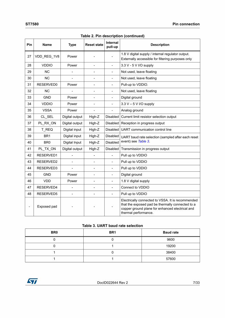
DocID022644 Rev 2 7/33
ST7580 Pin connection
33
27 VDD_REG_1V8 Power - -1.8 V digital supply / internal regulator output.
Externally accessible for filtering purposes only
28 VDDIO Power - - 3.3 V - 5 V I/O supply
29 NC - - - Not used, leave floating
30 NC - - - Not used, leave floating
31 RESERVED0 Power - - Pull-up to VDDIO.
32 NC - - - Not used, leave floating
33 GND Power - - Digital ground
34 VDDIO Power - - 3.3 V – 5 V I/O supply
35 VSSA Power - - Analog ground
36 CL_SEL Digital output High-Z Disabled Current limit resistor selection output
37 PL_RX_ON Digital output High-Z Disabled Reception in progress output
38 T_REQ Digital input High-Z Disabled UART communication control line
39 BR1 Digital input High-Z Disabled UART baud rate selection (sampled after each reset event) see Table 3.40 BR0 Digital Input High-Z Disabled
41 PL_TX_ON Digital output High-Z Disabled Transmission in progress output
42 RESERVED1 - - - Pull up to VDDIO
43 RESERVED2 - - - Pull up to VDDIO
44 RESERVED3 - - - Pull up to VDDIO
45 GND Power - - Digital ground
46 VDD Power - - 1.8 V digital supply
47 RESERVED4 - - - Connect to VDDIO
48 RESERVED5 - - - Pull up to VDDIO
- Exposed pad - - -
Electrically connected to VSSA. It is recommended that the exposed pad be thermally connected to a copper ground plane for enhanced electrical and thermal performance.
Table 2. Pin description (continued)
Pin Name Type Reset stateInternalpull-up
Description
Table 3. UART baud rate selection
BR0 BR1 Baud rate
0 0 9600
0 1 19200
1 0 38400
1 1 57600
Maximum ratings ST7580
8/33 DocID022644 Rev 2
3 Maximum ratings
3.1 Absolute maximum ratings
3.2 Thermal data
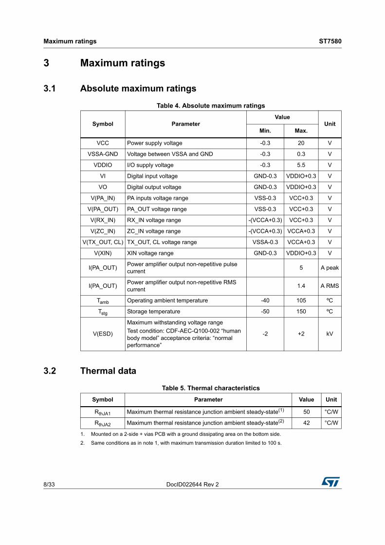
Table 4. Absolute maximum ratings
Symbol ParameterValue
UnitMin. Max.
VCC Power supply voltage -0.3 20 V
VSSA-GND Voltage between VSSA and GND -0.3 0.3 V
VDDIO I/O supply voltage -0.3 5.5 V
VI Digital input voltage GND-0.3 VDDIO+0.3 V
VO Digital output voltage GND-0.3 VDDIO+0.3 V
V(PA_IN) PA inputs voltage range VSS-0.3 VCC+0.3 V
V(PA_OUT) PA_OUT voltage range VSS-0.3 VCC+0.3 V
V(RX_IN) RX_IN voltage range -(VCCA+0.3) VCC+0.3 V
V(ZC_IN) ZC_IN voltage range -(VCCA+0.3) VCCA+0.3 V
V(TX_OUT, CL) TX_OUT, CL voltage range VSSA-0.3 VCCA+0.3 V
V(XIN) XIN voltage range GND-0.3 VDDIO+0.3 V
I(PA_OUT)Power amplifier output non-repetitive pulse current
5 A peak
I(PA_OUT)Power amplifier output non-repetitive RMS current
1.4 A RMS
Tamb Operating ambient temperature -40 105 ºC
Tstg Storage temperature -50 150 ºC
V(ESD)
Maximum withstanding voltage range
Test condition: CDF-AEC-Q100-002 “human body model” acceptance criteria: “normal performance”
-2 +2 kV
Table 5. Thermal characteristics
Symbol Parameter Value Unit
RthJA1 Maximum thermal resistance junction ambient steady-state(1)
1. Mounted on a 2-side + vias PCB with a ground dissipating area on the bottom side.
50 °C/W
RthJA2 Maximum thermal resistance junction ambient steady-state(2)
2. Same conditions as in note 1, with maximum transmission duration limited to 100 s.
42 °C/W

ST
758
0E
lectric
al c
hara
cteristics
Do
cID0
22644 R
ev 29/33
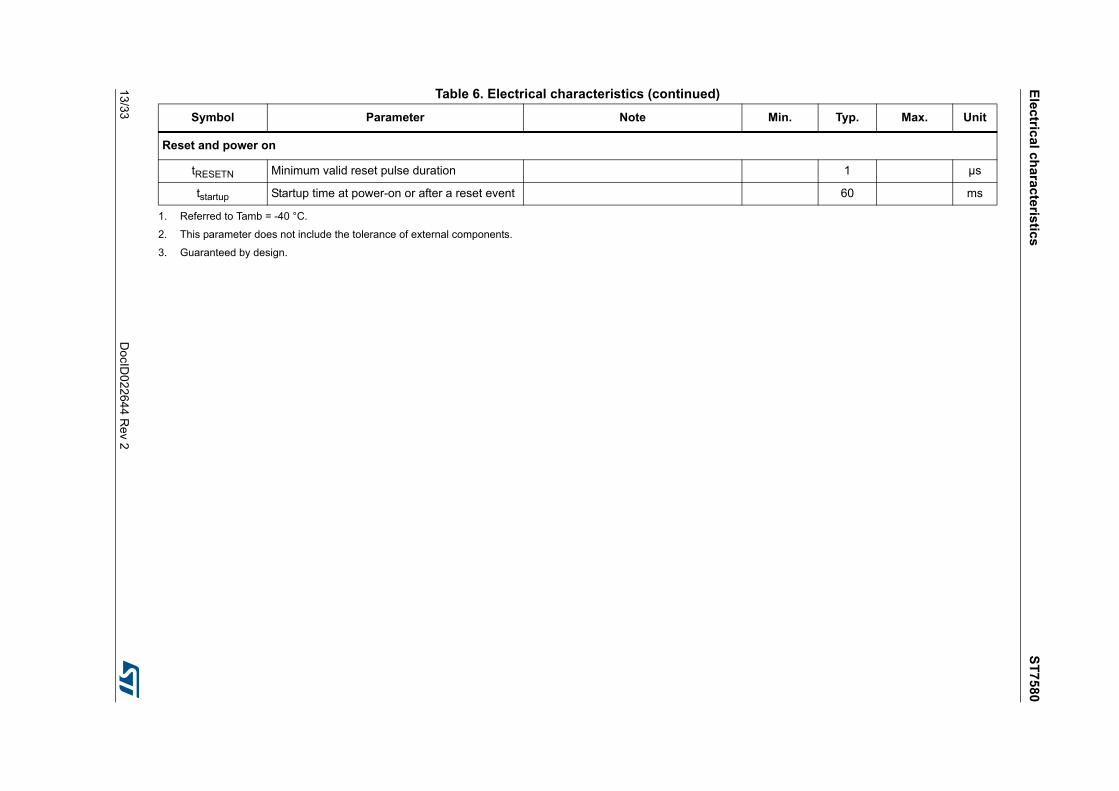
4 Electrical characteristics
TA = -40 to +105 °C, TJ < 125 °C, VCC = 18 V, unless otherwise specified.
Table 6. Electrical characteristics
Symbol Parameter Note Min. Typ. Max. Unit
Power supply
VCC Power supply voltage 8 13 18 V
I(VCC) RX Power supply current - Rx mode VCCA externally supplied 0.35 0.5 mA
I(VCC) TX Power supply current - Tx mode, no load VCCA externally supplied 22 30 mA
VCC UVLO_TL VCC undervoltage lockout low threshold 6.1 6.5 6.95 V
VCC UVLO_TH VCC undervoltage lockout high threshold 6.8 7.2 7.5 V
VCC UVLO_HYST VCC undervoltage lockout hysteresis 250 (1) 700 mV
I(VCCA) RX Analog supply current - Rx mode 5 6 mA
I(VCCA) TX Analog supply current - Tx mode V(TX_OUT) = 5 V p-p, no load 8 10 mA
VDD Digital core supply voltage Externally supplied -10% 1.8 +10% V
I(VDD) Digital core supply current 35 41 mA
I(VDD) RESET Digital core supply current in RESET state 8 mA
VDD_PLL PLL supply voltage VDD V
I(VDD_PLL) PLL supply current 0.4 0.5 mA
VDDIO Digital I/O supply voltage Externally supplied -10% 3.3 or 5 +10% V
VDDIO UVLO_TL
VDDIO undervoltage lockout low threshold 2.2 2.4 2.6 V
VDDIO
UVLO_THVDDIO undervoltage lockout high threshold 2.45 2.65 2.85 V
VDDIO
UVLO_HYSTVDDIO undervoltage lockout hysteresis 180 240 mV

Ele
ctrical ch
arac
teris
ticsS
T75
80
10/33D
ocID
02264
4 Rev 2
Analog front-end
Power amplifier
V(PA_OUT) BIAS Power amplifier output bias voltage - Rx mode VCC/2 V
GBWP Power amplifier gain-bandwidth product 100 MHz
I(PA_OUT) MAX Power amplifier maximum output current 1000mA rms
V(PA_OUT) TOL Power amplifier output tolerance(2) VCC = 18 V,
V(PA_OUT) = 14 V p-p (typ.),
V(PA_OUT) BIAS = VCC/2,
RLOAD=50 - see Figure 3
-3% +3%
V(PA_OUT) HD2 Power amplifier output 2nd harmonic distortion -70 -63 dBc
V(PA_OUT) HD3 Power amplifier output 3rd harmonic distortion -66 -63 dBc
V(PA_OUT) THD Power amplifier output total harmonic distortion 0.1 0.15 %
C(PA_IN) Power amplifier input capacitancePA_IN+ vs. VSS(3) 10 pF
PA_IN- vs. VSS(3) 10 pF
PSRR Power supply rejection ratio
50 Hz 100 dB
1 kHz 93 dB
100 kHz 70 dB
CL_TH Current sense high threshold on CL pin 2.25 2.35 2.4 V
CL_RATIO Ratio between PA_OUT and CL output current 80
Transmitter
V(TX_OUT) BIAS Transmitter output bias voltage - Rx mode VCCA/2 V
V(TX_OUT) MAX Transmitter output maximum voltage swing TX_GAIN = 31, no load 4.8 4.95 VCCA V p-p
TX_GAIN Transmitter output digital gain range 0 31
TX_GAIN TOL Transmitter output digital gain tolerance -0.35 0.35 dB
R(TX_OUT) Transmitter output resistance 1 k
V(TX_OUT) HD2 Transmitter output 2nd harmonic distortionV(TX_OUT) = V(TX_OUT) max. no load, T = 25 °C
-72 -67 dBc
Table 6. Electrical characteristics (continued)
Symbol Parameter Note Min. Typ. Max. Unit
ST
758
0E
lectric
al c
hara
cteristics
Do
cID0
22644 R
ev 211/33
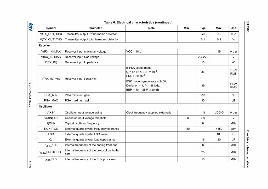
V(TX_OUT) HD3 Transmitter output 3rd harmonic distortion -70 -55 dBc
V(TX_OUT) THD Transmitter output total harmonic distortion 0.1 0.2 %
Receiver
V(RX_IN) MAX Receiver input maximum voltage VCC = 18 V 15 V p-p
V(RX_IN) BIAS Receiver input bias voltage VCCA/2 V
Z(RX_IN) Receiver input Impedance 10 k
V(RX_IN) MIN Receiver input sensitivity
B-PSK coded mode,
fC = 86 kHz, BER = 10-3,
SNR 20 db (3)36
dBµV RMS
FSK mode, symbol rate = 2400,
Deviation = 1, fC = 86 kHz,
BER = 10-3, SNR 20 dB
39dBµV RMS
PGA_MIN PGA minimum gain -18 dB
PGA_MAX PGA maximum gain 30 dB
Oscillator
V(XIN) Oscillator input voltage swing Clock frequency supplied externally 1.8 VDDIO V p-p
V(XIN) TH Oscillator input voltage threshold 0.8 0.9 1 V
f(XIN) Crystal oscillator frequency 8 MHz
f(XIN) TOL External quartz crystal frequency tolerance -150 +150 ppm
ESR External quartz crystal ESR value 100
CL External quartz crystal load capacitance 16 20 pF
fCLK_AFE Internal frequency of the analog front-end 8 MHz
fCLK_PROTOCOLInternal frequency of the protocol controller core
28 MHz
fCLK_PHY Internal frequency of the PHY processor 56 MHz
Table 6. Electrical characteristics (continued)
Symbol Parameter Note Min. Typ. Max. Unit

Ele
ctrical ch
arac
teris
ticsS
T75
80
12/33D
ocID
02264
4 Rev 2
Temperature sensor
T_TH1 Temperature threshold 1
(3)
63 70 77 °C
T_TH2 Temperature threshold 2 90 100 110 °C
T_TH3 Temperature threshold 3 112 125 138 °C
T_TH4 Temperature threshold 4 153 170 187 °C
Zero crossing comparator
V(ZC_IN) MAX Zero crossing detection input voltage range 10 V p-p
V(ZC_IN) TL Zero crossing detection input low threshold -40 -30 -20 mV
V(ZC_IN) TH Zero crossing detection input high threshold 30 40 50 mV
V(ZC_IN) HYST Zero crossing detection input hysteresis 62 70 78 mV
ZC_IN d.c. Zero crossing input duty cycle 50 %
Digital section
Digital I/O
RPULL-UP Internal pull-up resistorsVDDIO = 3.3 V 66 k
VDDIO = 5 V 41 k
VIH High logic level input voltage 0.65*VDDIO VDDIO+0.3 V
VIL Low logic level input voltage -0.3 0.35*VDDIO V
VOH High logic level output voltage IOH = -4 mA VDDIO-0.4 V
VOL Low logic level output voltage IOL = 4 mA 0.4 V
UART interface
Baud rate
-1.5% 57600 +1.5% BAUD
-1.5% 38400 +1.5% BAUD
-1.5% 19200 +1.5% BAUD
-1.5% 9600 +1.5% BAUD
Table 6. Electrical characteristics (continued)
Symbol Parameter Note Min. Typ. Max. Unit
Ele
ctrical ch
arac
teris
ticsS
T75
80
13/33D
ocID
02264
4 Rev 2
Reset and power on
tRESETN Minimum valid reset pulse duration 1 µs
tstartup Startup time at power-on or after a reset event 60 ms
1. Referred to Tamb = -40 °C.
2. This parameter does not include the tolerance of external components.
3. Guaranteed by design.
Table 6. Electrical characteristics (continued)
Symbol Parameter Note Min. Typ. Max. Unit

Electrical characteristics ST7580
14/33 DocID022644 Rev 2
Figure 3. Power amplifier test circuit
Figure 4. I(VCC) vs. I(PA_OUT) curve - typical values
0
50
100
150
200
250
300
350
400
450
500
550
0 100 200 300 400 500 600 700 800 900 1000 1100
I(PA_OUT) [mA]
I(V
CC
) [m
A]
AM11730v1

DocID022644 Rev 2 15/33
ST7580 Analog front-end (AFE)
33
5 Analog front-end (AFE)
5.1 Reception path
Figure 5 shows the block diagram of the ST7580 input receiving path. The main blocks are a wide input range analog programmable gain amplifier (PGA) and the analog to digital converter (ADC).
Figure 5. Reception path block diagram
The PGA is controlled by an embedded loop algorithm, adapting the PGA gain to amplify or attenuate the input signal according to the input voltage range for the ADC.
The PGA gain ranges from -18 dB up to 30 dB, with steps of 6 dB (typ.), as described in Table 7.
Table 7. PGA gain table
PGA code PGA gain (typ.) [dB] RX_IN max. range [V p-p]
0 -18 V(RX_IN) MAX
1 -12 8
2 -6 4
3 0 2
4 6 1
5 12 0.500
6 18 0.250
7 24 0.125
8 30 0.0625
AM02505v1
RX AFE
BPFADCRX_IN
BPFBPFADCADCPGAPGA
Analog front-end (AFE) ST7580
16/33 DocID022644 Rev 2
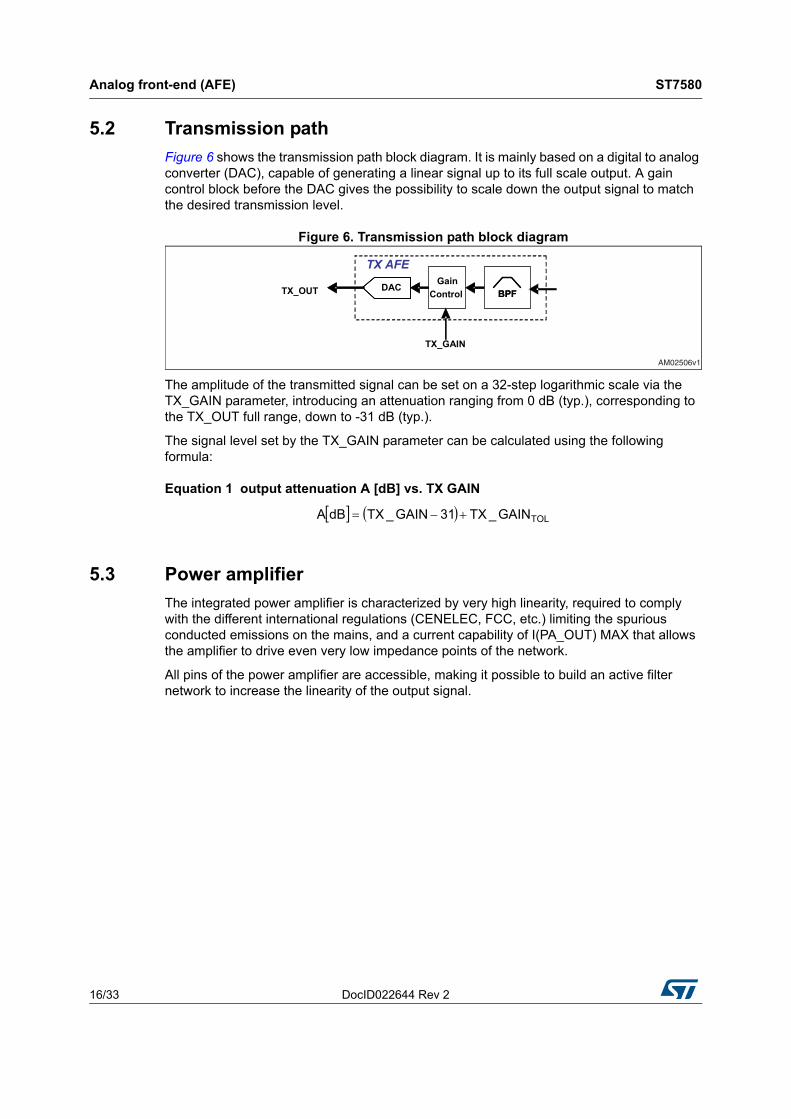
5.2 Transmission path
Figure 6 shows the transmission path block diagram. It is mainly based on a digital to analog converter (DAC), capable of generating a linear signal up to its full scale output. A gain control block before the DAC gives the possibility to scale down the output signal to match the desired transmission level.
Figure 6. Transmission path block diagram
The amplitude of the transmitted signal can be set on a 32-step logarithmic scale via the TX_GAIN parameter, introducing an attenuation ranging from 0 dB (typ.), corresponding to the TX_OUT full range, down to -31 dB (typ.).
The signal level set by the TX_GAIN parameter can be calculated using the following formula:
Equation 1 output attenuation A [dB] vs. TX GAIN
5.3 Power amplifier
The integrated power amplifier is characterized by very high linearity, required to comply with the different international regulations (CENELEC, FCC, etc.) limiting the spurious conducted emissions on the mains, and a current capability of I(PA_OUT) MAX that allows the amplifier to drive even very low impedance points of the network.
All pins of the power amplifier are accessible, making it possible to build an active filter network to increase the linearity of the output signal.
AM02506v1
TX AFE
DAC Gain ControlTX_OUT
TX_GAIN
BPFBPF
TOLGAIN_TX31GAIN_TXdBA

DocID022644 Rev 2 17/33
ST7580 Analog front-end (AFE)
33
5.4 Current and voltage control
The power amplifier output current sensing is performed by mirroring a fraction of the output current and making it flow through a resistor RCL connected between the CL pin and VSS. The following relationship can be established between V(CL) and I(PA_OUT):
Equation 2 V(CL) vs. I(PA_OUT)
The voltage level V(CL) is compared with the internal threshold CL_TH. When the V(CL) exceeds the CL_TH level, the V(TX_OUT) voltage is decreased by one TX_GAIN step at a time until V(CL) goes below the CL_TH threshold.
The current sense circuit is depicted in Figure 7.
Figure 7. PA_OUT current sense circuit
The RCL value to get the desired output current limit I(PA_OUT)LIM can be calculated as follows:
Equation 3 RCL calculation
Note that I(PA_OUT)LIM is expressed as peak current, so the corresponding RMS current is calculated according to the transmitted signal waveform. As FSK and PSK modulations have different crest factor values, different RCL values are required for the two modulations.
The RCL values, to get 1 A RMS output current limit, calculated with typical values for CL_TH and CL_RATIO parameters, are indicated in Table 8.
Table 8. CL resistor typical values
Parameter Description Value Unit
RCL
Resistor value for I(PA_OUT) max. = 1 A RMS = 1.41 A pk (FSK mode)
133
Resistor value for I(PA_OUT) max. = 1 A RMS = 2 A pk (PSK mode) 94
RATIO_CL
OUT_PAIRCLV CL
AM02507v1
PA
CL
VCC
CL
I(CL) = I(PA_OUT)/CL_RATIO
PAI(PA_OUT)
R
RATIO_CL/OUT_PAI
TH_CLR
LIMCL
Analog front-end (AFE) ST7580
18/33 DocID022644 Rev 2
The CL_SEL pin can be used to switch automatically the RCL resistor value according to the used modulation. If FSK modulation is selected, CL_SEL is forced to GND, while if PSK modulation is selected, CL_SEL is in high impedance state.
5.5 Thermal shutdown and temperature control
The ST7580 performs an automatic shutdown of the power amplifier circuitry when the internal temperature exceeds T_TH4. After a thermal shutdown event, the temperature must go below T_TH3 before the ST7580 power amplifier comes back into operation.
Moreover, a digital thermometer is embedded to identify the internal temperature in four zones, as indicated in Table 9.
Table 9. Temperature zones
5.6 Zero crossing comparator
The ST7580 device embeds an analog comparator with hysteresis, used for optional zero crossing detection and synchronization. It requires a bipolar (ac) analog input signal, synchronous to the mains voltage.
Temperature zone Temperature value
1 T < T_TH1
2 T_TH1 < T < T_TH2
3 T_TH2 < T < T_TH3
4 T > T_TH3

DocID022644 Rev 2 19/33
ST7580 Power management
33
6 Power management
Figure 8 shows the power supply structure for the ST7580. The ST7580 operates from two external supply voltages:
VCC (8 to 18 V) for the power amplifier and the analog section
VDDIO (3.3 or 5 V) for interface lines and digital blocks.
Two internal linear regulators provide the remaining required voltages:
5 V analog front-end supply: generated from the VCC voltage and connected to the VCCA pin
1.8 V digital core supply: generated from the VDDIO voltage and connected to VDD_REG_1V8 (direct regulator output) and VDD pins.
The VDD_PLL pin, supplying the internal clock PLL, must be externally connected to VDD through a ferrite bead for noise filtering purposes.
All supply voltages must be properly filtered to their respective ground, using external capacitors close to each supply pin, in accordance with the supply scheme depicted in Figure 8.
Note that the internal regulators connected to VDD_REG_1V8 and to VCCA are not designed to supply external circuitry; their outputs are externally accessible for filtering purposes only.
External connections between all VDD pins are not required.

Power management ST7580
20/33 DocID022644 Rev 2
Figure 8. Power supply internal scheme and external connections
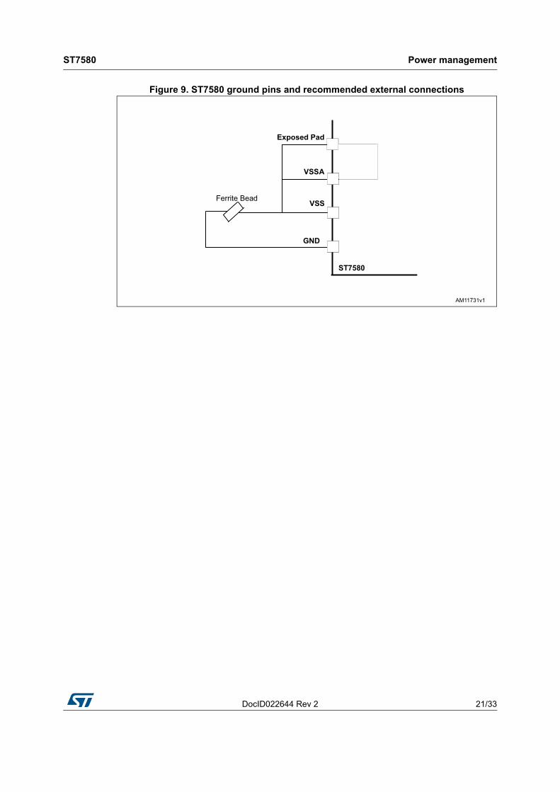
Ground connections
The ST7580 presents analog and digital ground connections. In particular, VSS is the power ground, VSSA is the analog ground, while GND pins refer to digital ground.
It is recommended to provide external connections between the ground pins as follows:
GND pins 6, 14, 33, and 45 are connected together;
VSSA pins 15 and 35 are connected to the exposed pad;
VSS is also connected to the exposed pad;
Connection between VSSA and GND is provided through a ferrite bead.
Ferrite Bead
LDO
LDO
AFE
DIGITAL INTERFACES
DIGITAL CORE
INTERNAL PLL
PA
VSS
VCCA
VSSA
VDD_REG_1V8
GND
VDD
VDD_PLL
VSSA
LDO
LDO
INTERNAL PLL
VCC
VDDIO
VSS
VCCA
VSSA
GND
AM02509v1
DocID022644 Rev 2 21/33
ST7580 Power management
33
Figure 9. ST7580 ground pins and recommended external connections

Clock management ST7580
22/33 DocID022644 Rev 2
7 Clock management
The main clock source is an 8 MHz crystal connected to the internal oscillator through the XIN and XOUT pins. Both XIN and XOUT pins have a 32 pF integrated capacitor, in order to drive a crystal having a load capacitance of 16 pF with no additional components.
Alternatively, an 8 MHz external clock can be directly supplied to the XIN pin, leaving XOUT floating.
A PLL internally connected to the output of the oscillator generates the fCLK_PHY, required by the PHY processor block engine. fCLK_PHY is then divided by two to obtain fCLK_PROTOCOL, required by the protocol controller.
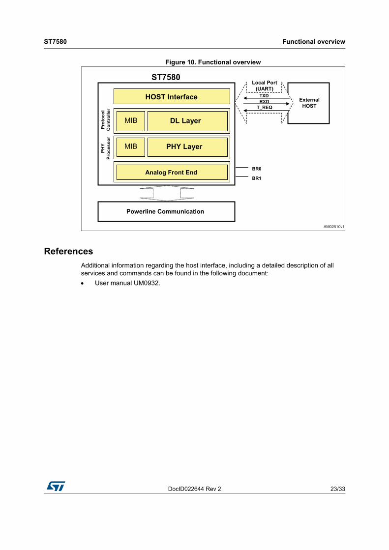
8 Functional overview
The ST7580 provides a complete physical layer (PHY) to the external host and some data link layer (DL) services for power line communication. It is mainly developed for smart metering applications in CENELEC A band, but suitable also for other command and control applications and remote load management in CENELEC B and D band.
A UART host interface is available for communication with an external host, exporting all the functions and services required to configure and control the device and its protocol stack.
The embedded PHY layer, hosted in the PHY processor, implements two different modulation schemes: a B-FSK modulation up to 9.6 kbps and a multi-mode PSK modulation with channel quality estimation, dual channel receiving mode, and convolutional coding, delivering a throughput up to 28.8 kbps.
The embedded DL layer hosted in the protocol controller offers framing and error correction services.
DocID022644 Rev 2 23/33
ST7580 Functional overview
33
Figure 10. Functional overview
References
Additional information regarding the host interface, including a detailed description of all services and commands can be found in the following document:
User manual UM0932.
AM02510v1
PHY Layer
HOST Interface PH
Y Pr
oces
sor
Prot
ocol
C
ontr
olle
r
DL Layer MIB
Local Port (UART)
TXD RXD
T_REQ
BR1
BR0
MIB
External HOST
Analog Front End
Powerline Communication
ST7580

Physical layer ST7580
24/33 DocID022644 Rev 2
9 Physical layer
The physical layer implemented in the ST7580 provides the following services:
Bit modulation and demodulation according to PSK and FSK schemes
Carrier selection up to 250 kHz
Bit, byte, and frame synchronization with training sequence and physical header
Signal to noise ratio (SNR) estimation.
9.1 PSK modulations
The ST7580 supports several PSK (phase shift keying) modulations with a symbol rate of 9600 baud. As all PSK modulations share the same physical frame, the receiver is able to recognize the PSK modulation kind used by the transmitter without further settings.
9.1.1 PSK modes
The ST7580 supports several PSK modes:
Uncoded modes: B-PSK, Q-PSK, 8-PSK
Coded modes: B-PSK coded, Q-PSK coded
B-PSK coded with peak noise avoidance (PNA) algorithm.
PSK coded modes transmit, on the power line, two coded bits for each information bit (code rate ½), halving the bit rate of the communication, but increasing the communication robustness through error correction.
B-PSK coded with the peak noise avoidance algorithm allows an even more robust communication and it is recommended to reject impulsive noise synchronous with the mains period. PNA modulation requires the transmitter to be synchronized to the mains period: the ZC_IN pin must be connected to a zero crossing detection circuit.
Table 10 summarizes all the available PSK modulations and their bit rate.
Table 10. PSK modes description
Modulation Symbol rate [baud] Information bits per symbol Bit rate [bps]
B-PSK 9600 1 9600
Q-PSK 9600 2 19200
8-PSK 9600 3 28800
B-PSK coded 9600 ½ 4800
Q-PSK coded 9600 1 9600
B-PSK coded PNA 9600 ¼ 2400

DocID022644 Rev 2 25/33
ST7580 Physical layer
33
9.1.2 PSK physical frame
Figure 11 shows the physical frame for PSK modulations.
Figure 11. PSK physical frame structure (length in bytes)
The meaning of each field is as follows:
Preamble: a sequence of alternating 1 and 0 symbols (AAh bytes) required by the receiver PLL to achieve bit synchronization. Its length is programmable from 2 to 5 bytes.
Unique word: a predefined sequence used to mark the start of a physical frame. The physical layer also provides SNR estimation on the received unique word.
Mode: indicates the PSK mode used for the physical SDU. Thanks to this byte, the receiver can automatically detect the PSK mode to be used to properly receive the physical SDU.
Physical SDU (service data unit): payload of the physical layer. Its length is specified in its first byte, which is always present.
Preamble, unique word, and mode fields are always transmitted using the B-PSK modulation. The physical layer SDU field can be sent according to any PSK modulation (B-PSK, Q-PSK, 8-PSK, B-PSK coded, Q-PSK coded, B-PSK coded PNA) expressed in the mode field.
9.2 FSK modulations
9.2.1 FSK options
The ST7580 supports several FSK (frequency shift keying) modulations with a symbol rate from 1200 to 9600 baud. Table 11 summarizes all the available FSK modulations and their bit rate.
The frequency deviation (f) is the difference between the carrier frequency and the FSK tone.
Table 11. FSK modes description
Modulation Symbol rate [baud] Information bits per symbol Bit rate [bps]
FSK @1200 1200 1 1200
FSK @2400 2400 1 2400
FSK @4800 4800 1 4800
FSK @9600 9600 1 9600

Physical layer ST7580
26/33 DocID022644 Rev 2
Figure 12. Frequency deviation
The following equation shows the frequency deviation formula for ST7580 FSK modulation:
Equation 4 Frequency deviation formula
The deviation factor is a configurable parameter: admitted values are 1 or 0.5. Table 12 summarizes the frequency deviation for all symbol rate and deviation factors.
Table 12. Frequency deviation possible values
Symbol rate [baud] Deviation factor
1 0.5
1200 0.6 kHz 0.3 kHz
2400 1.2 kHz 0.6 kHz
4800 2.4 kHz 1.2 kHz
9600 4.8 kHz 2.4 kHz
Hzfactor_deviation*2
rate_symbolf
DocID022644 Rev 2 27/33
ST7580 Physical layer
33
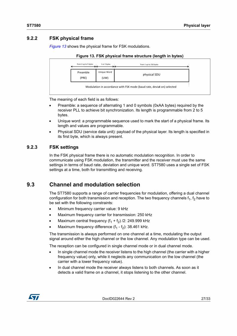
9.2.2 FSK physical frame
Figure 13 shows the physical frame for FSK modulations.
Figure 13. FSK physical frame structure (length in bytes)
The meaning of each field is as follows:
Preamble: a sequence of alternating 1 and 0 symbols (0xAA bytes) required by the receiver PLL to achieve bit synchronization. Its length is programmable from 2 to 5 bytes.
Unique word: a programmable sequence used to mark the start of a physical frame. Its length and values are programmable.
Physical SDU (service data unit): payload of the physical layer. Its length is specified in its first byte, which is always present.
9.2.3 FSK settings
In the FSK physical frame there is no automatic modulation recognition. In order to communicate using FSK modulation, the transmitter and the receiver must use the same settings in terms of baud rate, deviation and unique word. ST7580 uses a single set of FSK settings at a time, both for transmitting and receiving.
9.3 Channel and modulation selection
The ST7580 supports a range of carrier frequencies for modulation, offering a dual channel configuration for both transmission and reception. The two frequency channels f1, f2 have to be set with the following constraints:
Minimum frequency carrier value: 9 kHz
Maximum frequency carrier for transmission: 250 kHz
Maximum central frequency (f1 + f2) /2: 249.999 kHz
Maximum frequency difference (f1 - f2): 38.461 kHz.
The transmission is always performed on one channel at a time, modulating the output signal around either the high channel or the low channel. Any modulation type can be used.
The reception can be configured in single channel mode or in dual channel mode.
In single channel mode the receiver listens to the high channel (the carrier with a higher frequency value) only, while it neglects any communication on the low channel (the carrier with a lower frequency value).
In dual channel mode the receiver always listens to both channels. As soon as it detects a valid frame on a channel, it stops listening to the other channel.

Physical layer ST7580
28/33 DocID022644 Rev 2
In addition, during reception, each channel supports only a single modulation at a time, which can be one of the two listed below:
1. Any of the PSK modulations (specified by the mode field in PSK physical frame, Section 9.1.2)
2. FSK modulation, using the current FSK settings.
Table 13 shows the allowed combinations for single channel and dual channel reception mode. Note that in case of FSK modulation on one channel and PSK on the other, the maximum FSK symbol rate is limited to 2400 baud.
Table 13. ST7580 allowed settings combination for reception
Reception mode High channel Low channel
Single channel receiverAny PSK -
Selected FSK -
Dual channel receiver
Any PSK Any PSK
Selected FSK (2400 baud) Any PSK
Any PSK Selected FSK (2400 baud)
DocID022644 Rev 2 29/33
ST7580 Data link layer
33
10 Data link layer
The data link layer implemented in the ST7580 provides some basic services:
Encapsulation of user payloads into frames and frame delimitation
Error detection and canceling of corrupted frames
Sniffer functionality for corrupted frames
Encryption and authentication based on AES 128-bit algorithm
Traffic statistics.
10.1 Data link frame
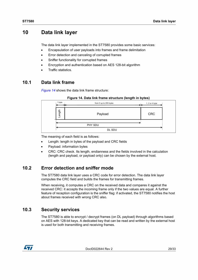
Figure 14 shows the data link frame structure:
Figure 14. Data link frame structure (length in bytes)
The meaning of each field is as follows:
Length: length in bytes of the payload and CRC fields
Payload: information bytes
CRC: CRC check. Its length, endianness and the fields involved in the calculation (length and payload, or payload only) can be chosen by the external host.
10.2 Error detection and sniffer mode
The ST7580 data link layer uses a CRC code for error detection. The data link layer computes the CRC field and builds the frames for transmitting frames.
When receiving, it computes a CRC on the received data and compares it against the received CRC: it accepts the incoming frame only if the two values are equal. A further feature of reception configuration is the sniffer flag: if activated, the ST7580 notifies the host about frames received with wrong CRC also.
10.3 Security services
The ST7580 is able to encrypt / decrypt frames (on DL payload) through algorithms based on AES with 128-bit keys. A dedicated key that can be read and written by the external host is used for both transmitting and receiving frames.

Package information ST7580
30/33 DocID022644 Rev 2
11 Package information
In order to meet environmental requirements, ST offers these devices in different grades of ECOPACK® packages, depending on their level of environmental compliance. ECOPACK specifications, grade definitions and product status are available at: www.st.com. ECOPACK is an ST trademark.
The ST7580 is hosted in a 48-pin thermally enhanced, very thin, fine pitch quad flat package no lead (VFQFPN) with exposed pad, which allows the device to dissipate the heat that is generated by the operation of the two linear regulators and the power amplifier.
11.1 VFQFPN48 (7 x 7 x 1.0 mm) package information
Figure 15. VFQFPN48 (7 x 7 x 1.0 mm) package outline
DocID022644 Rev 2 31/33
ST7580 Package information
33
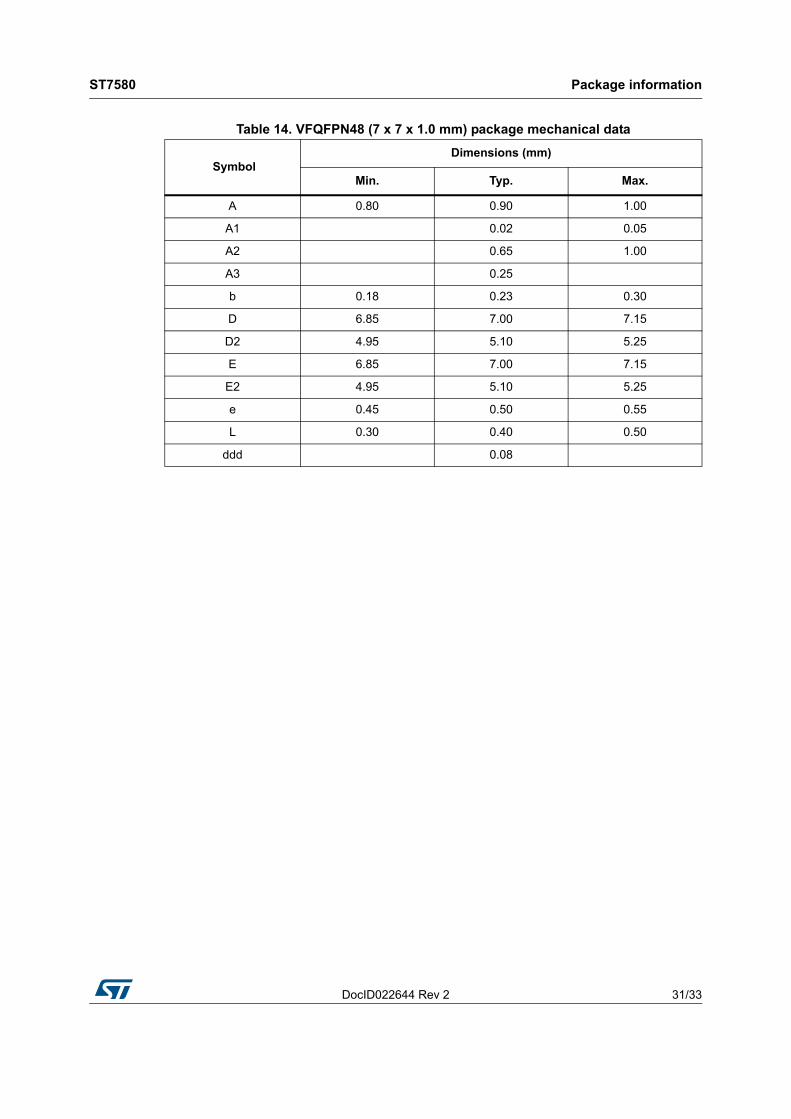
Table 14. VFQFPN48 (7 x 7 x 1.0 mm) package mechanical data
SymbolDimensions (mm)
Min. Typ. Max.
A 0.80 0.90 1.00
A1 0.02 0.05
A2 0.65 1.00
A3 0.25
b 0.18 0.23 0.30
D 6.85 7.00 7.15
D2 4.95 5.10 5.25
E 6.85 7.00 7.15
E2 4.95 5.10 5.25
e 0.45 0.50 0.55
L 0.30 0.40 0.50
ddd 0.08

Revision history ST7580
32/33 DocID022644 Rev 2
12 Revision history
Table 15. Document revision history
Date Revision Changes
26-Jan-2012 1 Initial release.
30-May-2016 2
Updated temperature operative range (replaced 85 by 105 °C) in Section : Features on page 1, Table 4: Absolute maximum ratings on page 8, and in Section 4: Electrical characteristics on page 9.Minor modifications throughout document.

DocID022644 Rev 2 33/33
ST7580
33
IMPORTANT NOTICE – PLEASE READ CAREFULLY
STMicroelectronics NV and its subsidiaries (“ST”) reserve the right to make changes, corrections, enhancements, modifications, and improvements to ST products and/or to this document at any time without notice. Purchasers should obtain the latest relevant information on ST products before placing orders. ST products are sold pursuant to ST’s terms and conditions of sale in place at the time of order acknowledgement.
Purchasers are solely responsible for the choice, selection, and use of ST products and ST assumes no liability for application assistance or the design of Purchasers’ products.
No license, express or implied, to any intellectual property right is granted by ST herein.
Resale of ST products with provisions different from the information set forth herein shall void any warranty granted by ST for such product.
ST and the ST logo are trademarks of ST. All other product or service names are the property of their respective owners.
Information in this document supersedes and replaces information previously supplied in any prior versions of this document.
© 2016 STMicroelectronics – All rights reserved
Top Related