


Languages
Pages
Legal

Focused IonBeam
ThomasGunthner
Generating aFIB
FIB-Applications
Presentation talk
FOCUSED ION BEAM(FIB)
Thomas Gunthner
TU Munchen
19th January 2009

Focused IonBeam
ThomasGunthner
Generating aFIB
FIB-Applications
Overview
1 Generating a focused ion beamIon sourcesIon optics
2 FIB-ApplicationsScanning ion microscopy (SIM)Focused ion beam lithography
ResistlithographyMicromachining
Focused IonBeam
ThomasGunthner
Generating aFIB
Ion sources
Ion optics
FIB-Applications
Generating a focused ionbeam

Focused IonBeam
ThomasGunthner
Generating aFIB
Ion sources
Ion optics
FIB-Applications
Sample of a FIB-system
Figure: http://www.fzd.de/db/PicOri?pOid=24361, 01/17/2009
Focused IonBeam
ThomasGunthner
Generating aFIB
Ion sources
Ion optics
FIB-Applications
Ion sources
Gas field ion source (GFIS)
Liquid metal ion source (LMIS)
(Plasma ion gun)
Focused IonBeam
ThomasGunthner
Generating aFIB
Ion sources
Ion optics
FIB-Applications
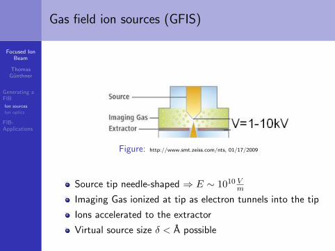
Gas field ion sources (GFIS)
Figure: http://www.smt.zeiss.com/nts, 01/17/2009
Source tip needle-shaped ⇒ E ∼ 1010 Vm
Imaging Gas ionized at tip as electron tunnels into the tip
Ions accelerated to the extractor
Virtual source size δ < A possible

Focused IonBeam
ThomasGunthner
Generating aFIB
Ion sources
Ion optics
FIB-Applications
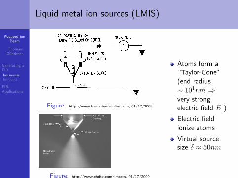
Liquid metal ion sources (LMIS)
Figure: http://www.freepatentsonline.com, 01/17/2009
Figure: http://www.ehdtg.com/images, 01/17/2009
Atoms form a“Taylor-Cone”(end radius∼ 101nm ⇒very strongelectric field E )
Electric fieldionize atoms
Virtual sourcesize δ ≈ 50nm
Focused IonBeam
ThomasGunthner
Generating aFIB
Ion sources
Ion optics
FIB-Applications
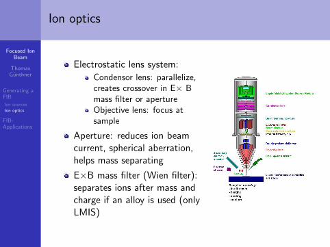
Ion optics
Electrostatic lens system:
Condensor lens: parallelize,creates crossover in E× Bmass filter or apertureObjective lens: focus atsample
Aperture: reduces ion beamcurrent, spherical aberration,helps mass separating
E×B mass filter (Wien filter):separates ions after mass andcharge if an alloy is used (onlyLMIS)

Focused IonBeam
ThomasGunthner
Generating aFIB
Ion sources
Ion optics
FIB-Applications
Further features
Deflector plates: Steering ionbeam over sample with eletricfields in x- and y-direction(compare oscilloscope)
Beam blanker: Deflects ionbeam so much that it will notpenetrate the sample
Focused IonBeam
ThomasGunthner
Generating aFIB
FIB-Applications
SIM
FIB lithography
Resistlithography
Micromachining
FIB-Applications

Focused IonBeam
ThomasGunthner
Generating aFIB
FIB-Applications
SIM
FIB lithography
Resistlithography
Micromachining
Scanning ion microscopy (SIM)
SIM is very similar to SEM (see electron microscopy)
Figure: http://www.crystaltexture.com/jpg 01/17/2009
Detected particles: low-energy secondary electrons(< 10eV ), secondary ions and photons
Focused IonBeam
ThomasGunthner
Generating aFIB
FIB-Applications
SIM
FIB lithography
Resistlithography
Micromachining
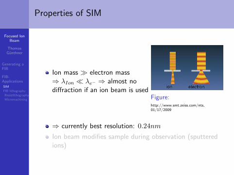
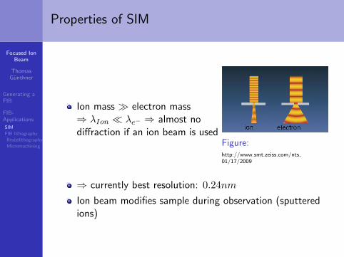
Properties of SIM
Ion mass � electron mass⇒ λIon � λe− ⇒ almost nodiffraction if an ion beam is used
Figure:http://www.smt.zeiss.com/nts,01/17/2009
⇒ currently best resolution: 0.24nmIon beam modifies sample during observation (sputteredions)
Focused IonBeam
ThomasGunthner
Generating aFIB
FIB-Applications
SIM
FIB lithography
Resistlithography
Micromachining
Properties of SIM
Ion mass � electron mass⇒ λIon � λe− ⇒ almost nodiffraction if an ion beam is used
Figure:http://www.smt.zeiss.com/nts,01/17/2009
⇒ currently best resolution: 0.24nmIon beam modifies sample during observation (sputteredions)

Focused IonBeam
ThomasGunthner
Generating aFIB
FIB-Applications
SIM
FIB lithography
Resistlithography
Micromachining
Properties of SIM
Secondary electrons much moresensitive to details of surfacestructure in the target than inSEM, sensitive to work functionof surface
Using ion-induced secondaryions and electrons to gain muchinformation of the sample
Chemical surface analysis bymeans of secondary ions
Figure:http://bp1.blogger.com/rWWz5HvJNko/RYVRwwxZ2I/AAAAAAAAABE,01/17/2009
Focused IonBeam
ThomasGunthner
Generating aFIB
FIB-Applications
SIM
FIB lithography
Resistlithography
Micromachining
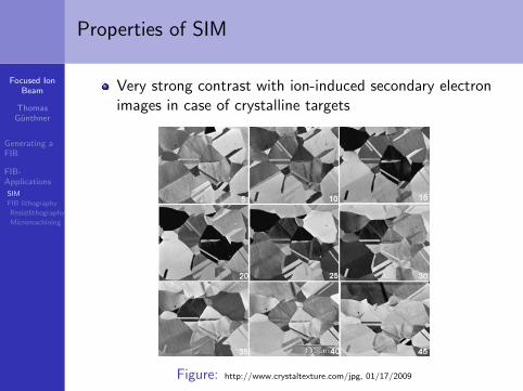
Properties of SIM
Very strong contrast with ion-induced secondary electronimages in case of crystalline targets
Figure: http://www.crystaltexture.com/jpg, 01/17/2009
Focused IonBeam
ThomasGunthner
Generating aFIB
FIB-Applications
SIM
FIB lithography
Resistlithography
Micromachining
Focused ion beam lithography (FIBL)
FIBL includes:
Resistlithography
Micromachining
Focused IonBeam
ThomasGunthner
Generating aFIB
FIB-Applications
SIM
FIB lithography
Resistlithography
Micromachining
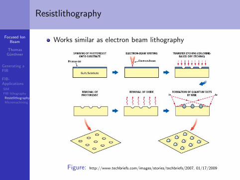
Resistlithography
Works similar as electron beam lithography
Figure: http://www.techbriefs.com/images/stories/techbriefs/2007, 01/17/2009

Focused IonBeam
ThomasGunthner
Generating aFIB
FIB-Applications
SIM
FIB lithography
Resistlithography
Micromachining
Resistlithography
Thickness of resist adjusted to range of ion beam
Avoid doping by using a two layer resist system
No proximity effect (compare e-beam)
Possible resolution: 20− 30nm
Focused IonBeam
ThomasGunthner
Generating aFIB
FIB-Applications
SIM
FIB lithography
Resistlithography
Micromachining
Micromachining
Creating nanometer structures by
sputtering material from a surface
induce deposition on a surface
Applications:
Failure analysis
Lithographic mask repair
Modification and repair of integrated circuits
Focused IonBeam
ThomasGunthner
Generating aFIB
FIB-Applications
SIM
FIB lithography
Resistlithography
Micromachining
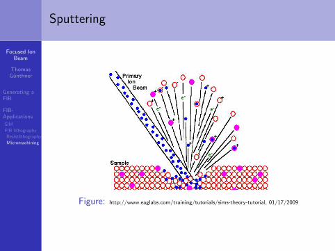
Sputtering
Figure: http://www.eaglabs.com/training/tutorials/sims-theory-tutorial, 01/17/2009

Focused IonBeam
ThomasGunthner
Generating aFIB
FIB-Applications
SIM
FIB lithography
Resistlithography
Micromachining
Sputtering
Figure: Walter Schottky Institut, E24
Focused IonBeam
ThomasGunthner
Generating aFIB
FIB-Applications
SIM
FIB lithography
Resistlithography
Micromachining
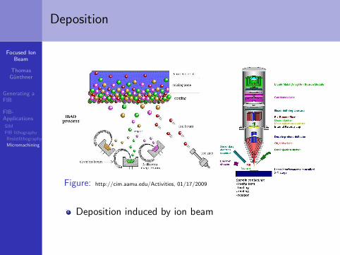
Deposition
Figure: http://cim.aamu.edu/Activities, 01/17/2009
Deposition induced by ion beam

Focused IonBeam
ThomasGunthner
Generating aFIB
FIB-Applications
SIM
FIB lithography
Resistlithography
Micromachining
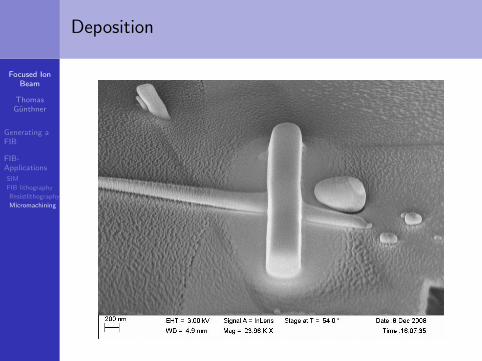
Deposition
Figure: Walter Schottky Institut, E24
Focused IonBeam
ThomasGunthner
Generating aFIB
FIB-Applications
SIM
FIB lithography
Resistlithography
Micromachining
Deposition

Focused IonBeam
ThomasGunthner
Generating aFIB
FIB-Applications
Literature
J.Orloff, High-resolution focused ion beams, Rev.Sci.Instrum.64,1105(1993)
M. Hillmann, 3-dimensionale Nanostrukturierung mittels fokussierterIonenstrahllithographie, (2001)
http://www.smt.zeiss.com
http://www.freepatentsonline.com/6531811-0-large.jpg
http://physics.pdx.edu/ esanchez/Research/ChargedBeam
http://www.ehdtg.com/images
http://www.fzd.de/db/PicOri?pOid=24361
http://bp1.blogger.com/rWWz5HvJNko/
http://www.crystaltexture.com/jpg
http://www.techbriefs.com/images/stories/techbriefs/2007
http://cim.aamu.edu/Activities
Top Related