


Languages
Pages
Legal


Electronic Circuits LaboratoryEE462GLab #3
Diodes, Transfer Characteristics, and Clipping Circuits

Instrumentation
This lab requires: Function Generator and
Oscilloscope (as in Lab 1) Tektronix’s PS 280 DC Triple
output (one fixed 5V / 3A and 2 variable 0 to 30V / 2A) Power Supply
What advantages are there to a chassis ground over an earth ground for a power supply?
chassis ground

Instrumentation
The 2 variable outputs of the power supply will be used for batteries (DC series sources) in the experiments’ circuits:
10k Vs Vout
V1
+
-
V2
Minus Terminal
Plus Terminal
LET CHASSIS GROUND FLOAT!

Ideal Diode Model Diode junction acts as a short circuit for forward
bias (VD > 0 (anode positive)).
Diode junction acts as an open circuit for reverse bias (VD < 0 (anode negative)).
Near-Ideal Diode Model Add a 0.7 voltage source for the forward offset
voltage in series ideal diode with same polarity as the forward bias.
Ideal Diode Model
Anode Cathode
+ Vd = 0 -Id
Diode On
Anode Cathode
+ Vd -Id 0.7 V
Anode Cathode
- Vd +Id = 0
Diode Off

Analysis of Diode Circuit
Methods of Analysis: Load-line analysis Diode-State Analysis SPICE
Diode-State Analysis Determine the on-off state of each diode by guessing a
combination of on-off states. For on-diodes assume a forward biased current direction (0 volts)
and for off-diodes assume a negative anode voltage (0 amps) and then analyze circuit.
If guessed state results in an inconsistent voltage or current in circuit analysis, guess another state combination until all are consistent with circuit analysis.

Problem: Use near-ideal model to
determine the state of diode D1 when V1=10V. (First guess diode is off).
Find range of V1 values such that D1 is off.
Assume output is current I3 and input is V1, analytically find the transfer characteristics of this circuit.
Solve via SPICE and plot:
Example
V1
R1 1k
D1 R
2 1
k
R3
1k
I3
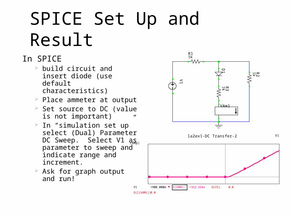
In SPICE build circuit and insert
diode (use default characteristics)
Place ammeter at output Set source to DC (value is
not important) In “simulation set up”
select (Dual) Parameter DC Sweep. Select V1 as parameter to sweep and indicate range and increment.
Ask for graph output and run!
SPICE Set Up and Result
V1
R1 1k
D1 R
2 1
k
R3
1k
VAm1
V1 +900.000m I(VAM1) +352.554n D(V1) 0.0
D(I(VAM1)) 0.0
la2ex1-DC Transfer-2 V1
(Amp)
0.0
+1.000m
-4.000 -2.000 0.0 +2.000 +4.000

Example
Sketch output waveform if input is a 5Vrms sinusoid of frequency 1kHz: Determine transfer
characteristics from input through waveform output.
Map input waveform through the transfer characteristics.
Note that when diode is on:
k
VI
3
4.113
0 0.5 1 1.5 2 2.5 3 3.5 4 4.5
x 10-3
-8
-6
-4
-2
0
2
4
6
8Input Voltage
seconds
Vo
lts
1.4 Volts
7.07 Volts
0 0.5 1 1.5 2 2.5 3 3.5 4 4.5
x 10-3
0
0.2
0.4
0.6
0.8
1
1.2
1.4
1.6
1.8
2x 10
-3 Output Current
seconds
Am
ps

Example with SPICE
Find output waveform if input is a 5Vrms sinusoid of frequency 1kHz: Build circuit in SPICE Set source to sinusoid, but do not check AC box. Go to transient
parameters tab and select appropriate amplitude (7.0711) and frequency (1000), the rest can be zero.
Set up simulation parameters, select “Parameter sweep of transient,” select source with start and stop magnitudes to same value and step size to a non zero number (you don’t want it to sweep, and it will not use these number since AC box was not check in source set up).
The set up transient parameters to appropriate start and stop time and increment.
The run simulation. If too many waveform periods appear, such that waveform details cannot be easily seen, make start and stop time shorter.

Example with SPICE
Find output waveform if input is a 5Vrms sinusoid of frequency 1kHz:
TIME -1.000 I(VAM1) -1.000 D(TIME) -1.000
D(I(VAM1)) -2.753
la2ex2--6 time (s)
(Amp)
0.0
+1.000m
+2.000m
0.0 +2.000m +4.000m +6.000m +8.000m +10.000m

Problem: Given Vs is a 2.8 Vrms 250Hz sinusoid,
find Vout (for power analysis a 5.1k load will also be considered)
Analysis: Use .7 V forward offset voltage and ideal
diode approximation. Can derive transfer characteristics or reason out directly.
Lab Procedure: Describe function generator settings,
oscilloscope probe placement, and oscilloscope settings. Record resulting waveforms for at least one period but not more than 5 (can use GPIB Program “Show_Wave” or save to a floppy disc).
Test Circuit A
10k Vs Vout
(A)
+
-

Test Circuit B
Problem: Given Vs is a 2.8 Vrms 250Hz sinusoid,
find Vout without a load.Analysis:
Use estimated forward offset voltage and ideal diode approximation. Can derive transfer characteristics or reason out directly.
Lab Procedure: Describe function generator settings,
power supply attachment with grounding issues, oscilloscope probe placement, and oscilloscope settings. Record resulting waveforms for at least one period but not more than 5. For the power analysis when circuit has a load, the DMM can be put in series with each branch to measure RMS current.
10k Vs Vout
V1
+
-

Test Circuit C
Problem: Given Vs is a 2.8 Vrms 250Hz
sinusoid, find Vout without a load
Analysis: Use estimated forward offset voltage
and ideal diode approximation. Can derive transfer characteristics or reason out directly.
Lab Procedure: Describe function generator settings,
power supply attachment and grounding issues, oscilloscope probe placement, and oscilloscope settings. Record resulting waveforms for at least one period but not more than 5.
10k Vs Vout
V1
+
-
V2
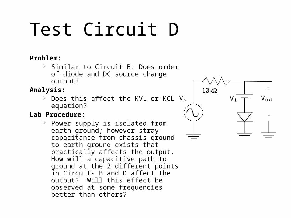
Test Circuit D
Problem: Similar to Circuit B: Does order of diode
and DC source change output?Analysis:
Does this affect the KVL or KCL equation?
Lab Procedure: Power supply is isolated from earth
ground; however stray capacitance from chassis ground to earth ground exists that practically affects the output. How will a capacitive path to ground at the 2 different points in Circuits B and D affect the output? Will this effect be observed at some frequencies better than others?
10k Vs Vout V1
+
-

Power: Recall instantaneous power is a product of the voltage and current
waveforms. So for source power find Vs and Is waveforms for one period and multiply point per point:
Recall average power is the integral of the instantaneous power divided by the period:
For sinusoid waveforms the integral reduces to:
Is power absorbed by an ideal diode?Analysis:
A Thévenin equivalent circuit around the nonlinear component in the circuit may be helpful in explaining changes due to load resistances.
Other Notes
)()()( titvtp ss
)cos(2
1)cos( ivivrmsrmsav VIIVP
T ssav dttitv
TP )()(
1

Stray Capacitance Models
Vs
10 k
+
Vout
-
V1
In reverse bias mode, a practical diode can be considered as a stray capacitance in parallel with open circuit.The power supply can be considered as a DC source with parallel capacitance to ground.
Cd
Cps
Compute effective capacitance over Vout

Stray Capacitance Models
Vs
10 k
+
Vout
-
Reverse order of power supply and diode in previous circuit and consider effects of stray capacitance.
Cps
Compute effective capacitance over Vout
Cd

Problem: Use range of V1 values for D1 is
off and on, as derived in previous problem, to find expressions of all branch currents (over full cycle of excitation waveform).
Determine power absorbed/supplied by each element.
Power Analysis Example
V1
R1 1k
D1 R
2 1
k
R3
1k
I3
I1
I2

Waveforms for currents if input is a 5Vrms sinusoid of frequency 1kHz: Branch currents:
Branch Currents
k
VI
3
7.02 11
k
VI
3
4.113
0 0.5 1 1.5 2 2.5 3 3.5 4 4.5
x 10-3
-8
-6
-4
-2
0
2
4
6
8Input Voltage
seconds
Vo
lts
1.4 Volts
7.07 Volts
k
VI
3
7.012
For V1 > 1.4
k
VI
21
1
03 I
k
VI
21
2
For V1 ≤ 1.4
t1 t2Time interval for V1 > 1.4
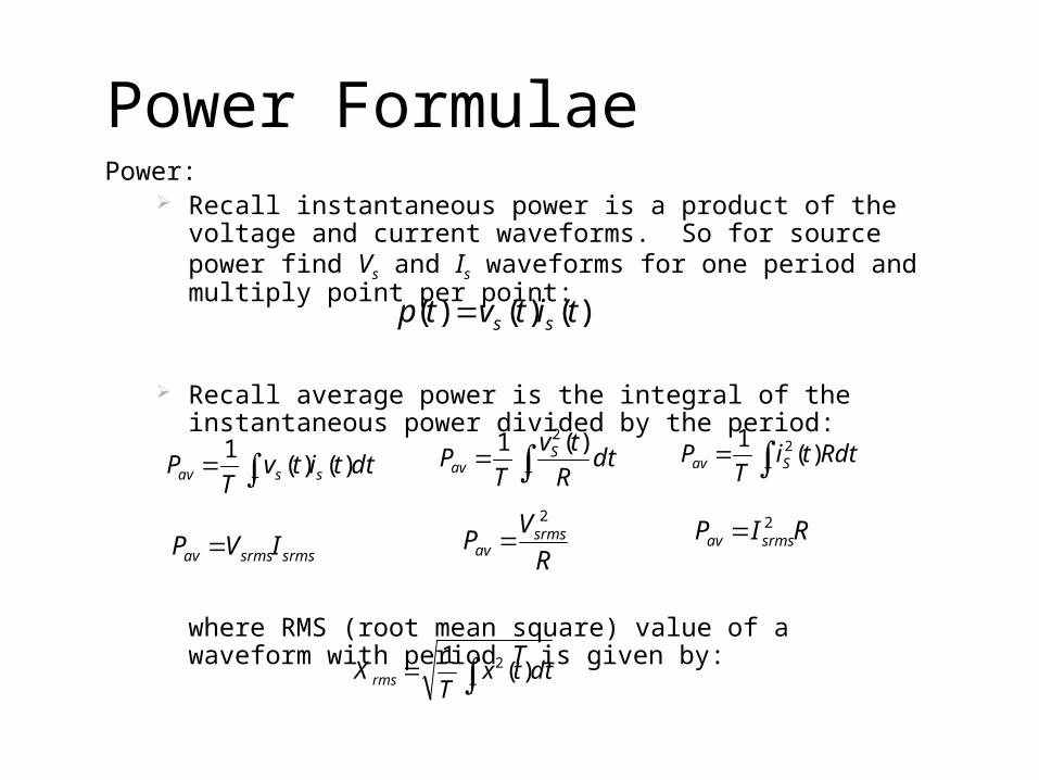
Power: Recall instantaneous power is a product of the voltage and current
waveforms. So for source power find Vs and Is waveforms for one period and multiply point per point:
Recall average power is the integral of the instantaneous power divided by the period:
where RMS (root mean square) value of a waveform with period T is given by:
Power Formulae
)()()( titvtp ss
TSav Rdtti
TP )(
1 2
T ssav dttitv
TP )()(
1
T
Sav dt
R
tv
TP
)(1 2
srmssrmsav IVP R
VP srmsav
2
RIP srmsav2
T
rms dttxT
X )(1 2

For V, the RMS values for source and branch currents are
RMS Circuit Values
51 rmsV
mAdttv
dttv
TI
tT
t
t
t
rms 21.22000
)(
3000
7.0)(1 1
2
2
1
2
1
2
12
)2000sin(25)(1 ttv
mAdttv
dttv
TI
tT
t
t
t
rms 83.22000
)(
3000
7.0)(21 1
2
2
1
2
1
2
11
mAdttv
TI
t
t
rms 89.03000
4.1)(1 2
1
2
13

For each element in the circuit the power is:
Note that power delivered is equal to power absorbed(Matlab script for evaluating integrals and power values is on next slide)
Power Analysis
mWIVP rmsrmsavv 2.14111 mWkIP rmsavR 0.8)1(211
mWkIP rmsavR 8.0)1(233
mWkIP rmsavR 9.4)1(222
mWVIP rmsavD 6.0)7.0(31
Power Supplied Power Absorbed

Matlab Symbolic Computations%define symbol for equation analysissyms t% Compute intersection of sine with the 1.4 voltage amplitudet1 = solve('5*sqrt(2)*sin(2*pi*1e3*t) = 1.4', t)% Define expression for source voltage as function of tv1 = 5*sqrt(2)*sin(2*pi*1e3*t)% define period of signaltp = 1e-3% Compute other intersection point of sine with the 1.4 volt level t2 = tp/2 - t1% Integrate for rms currentsi1rms = sqrt(int(((2*v1-0.7)/3e3)^2,t,t1,t2)/tp + int((v1/2e3)^2,t,t2,tp+t1)/tp)i2rms = sqrt(int(((v1+0.7)/3e3)^2,t,t1,t2)/tp + int((v1/2e3)^2,t,t2,tp+t1)/tp)i3rms = sqrt(int(((v1-1.4)/3e3)^2,t,t1,t2)/tp)% RMS source voltagev1rms = 5% Power delivered by source%pavsource = int(v1*(2*v1-.7)/3e3,t,t1,t2)/tp +int(v1*v1/2e3,t,t2,tp+t1)/tppavsource = v1rms*i1rms% Compute powers in all components (all resistors were 1e3 ohms)pavr1 = i1rms^2*1e3 % Resistor 1 powerpavdiode = i3rms*.7 % Diode powerpavr3 = i3rms^2*1e3 % Resistor 2 powerpavr2 = i2rms^2*1e3 % Resistor 3 power% by conservation of power all absorbing components should add up to power deliveredpavabsorbed = pavr1+pavr2+pavr3+pavdiodedisp(['Compare power absorbed: ' num2str(double(pavabsorbed)) 'W to power supplied: ' num2str(double(pavsource)) 'W'])

Final Notes
Data Sheet Make up a Data Sheet before coming to class and fill in
measurement in an orderly fashion. All general comments from previous labs apply.
Procedure Description Address all questions asked in the lab assignment sheet and lecture
that pertain to the procedure of making a measurement and getting the requested quantity.
Grounding issues are discussed in this section if they complicate probes placement.
Discuss how the forward offset voltage is determined from the measurements made of the V-I diode transfer characteristics.
All general comments from previous labs apply.

Final Notes
Discussion of Results Respond to all bold face comments and questions in the lab
assignment in this section. Explain why the waveforms appear as they do from diode theory and
measurement issues. Make comparisons between measured values when appropriate (i.e. if something changes in the circuit, how does this affect the output!)
Conclusion Briefly sum up results and indicate what was learned through doing
this experiment. Respond directly to the lab objectives. General
Number all figures, tables, and equations sequentially (learn how to use equation editors), and avoid first person voice.
Describe all figures and table in text. What are the important features the reader should see?
Top Related