


Languages
Pages
Legal

micro corp. EGS002 Datasheets EG8010 demo board
Copyright 2014©EGmicro corp. www.EGmicro.com
1 / 6
EGS002 Sinusoid Inverter Driver Board User Manual
1. Description EGS002 is a driver board specific for single phase sinusoid inverter. It uses ASIC EG8010 as
control chip and IR2110S as driver chip. The driver board integrates functions of voltage, current and temperature protection, LED warning indication and fan control.Jumper configures 50/60Hz AC output, soft start mode and dead time. EGS002 is an improved version of EGS001 that is compatible of EGS001’s original interfaces. EGS002 also integratescross-conduction prevention logic to enhance its ability of anti-interference, and LCD display interface for users’ convenience to use chip’s built-in display function.
EG8010 is a digital pure sine wave inverter ASIC (Application Specific Integrated Circuit) with complete function of built-in dead time control. It applies to DC-DC-AC two stage power converter system or DC-AC single stage low power frequency transformer system for boosting. EG8010 can achieve 50/60Hz pure sine wave with high accuracy, low harmonic and distortion by external 12MHz crystal oscillator. EG8010 is a CMOS IC that integrates SPWM sinusoid generator, dead time control circuit, range divider,soft start circuit, circuit protection, RS232 serial communication, 12832 serial LCD unit, and etc.
2. Circuit Schematic
EGS002 Driver Board Schematic
Figure 2‐1. EGS002 Sinusoid Inverter Driver Board Schematic
Y112M
C7 22P
C1 22P
D1
R11K
1
2
3
4
5
6
7
8
9
10
11
12
13
14
15
16
17
P1
C6
0.1uF
C5
10uF/16VD2FR107
R11
4.7ΩR13
10K
D4 IN4148
V1IRF840
C222.2uF
C230.1uF
R19
200KR2110K
RT1
NTC/10K
C340.01uF
1 2 3 4
8
+-
+-
7 56
U4LM393
R410K
R61.5K
C1710uF/16V
C191000P
C200.01uF
C14
0.1uF
C13
10uF/16V
C90.1uF
C1010uF/16V
C410uF/16V
R12
4.7ΩR14
10K
D5 IN4148
V2IRF840
R15
4.7ΩR17
10K
D6 IN4148
V3IRF840
R16
4.7ΩR18
10K
D7 IN4148
V4IRF840
R1010K
C301000P
R510K
C180.1uF
R3
100Ω
C160.1uF
FANCTR
TFB
VFB
+5V
GND
+12V
GND
2HO
VS2
2LO
GND
1HO
VS1
GND
1LO
GND
IFB
R2
100Ω
R7
1K
C211000P
C150.1uF
温度反馈
电流反馈
电压反馈
+5V +12V
R25
2.2K
Q1
8050
+400V
正弦220V输出
R2310K
0.1Ω
R24康铜丝
F1
散热风扇
大于45°开启风扇
小于40°关闭风扇
温度传感器+12V
+12V
+5V
+5V
+5V
+5V
+5V
+5V
+5V
EG8010.IR2110正弦波逆变器
驱动电路原理图(单极性调制方式)
L P2
N P3
LED
50/60Hz选择
D1状态指示灯说明正常:长亮过流:闪烁2下,灭2秒,一直循环过压:闪烁3下,灭2秒,一直循环欠压:闪烁4下,灭2秒,一直循环过温:闪烁5下,灭2秒,一直循环
正弦波输出电压调整
+0.65V
12345678
910
1112
1314
1516
17 18 19 20 21 22 23 24
2526
2728
2930
3132
NC
NC
LC
DC
LK
VCC
SPWMOUT1
SPWMOUT2
SPWMOUT3
SPWMOUT4
LCDEN
VVVF
DT
1
DT
0
LCDDI
GN
D
RX
D
TX
D
SPWM
EN
FAN
CT
R
LE
DO
UT
PWMTYP
OSC1
OSC2
GND
VFB
IFB
TFB
FRQADJ/VFB2 FRQ
SEL
0
FRQ
SEL
1
MO
DSE
L
SST
VR
EF
U2EG8010
L1
LO
COM
VCC
NC
NC
VS
VB
HO9
10
11
12
13
14
NC
NC
VDD
HIN
SD
LIN
15
16
VSS
NC 1
2
3
4
5
6
7
8
U1
IR21
10S
LO
COM
VCC
NC
NC
VS
VB
HO9
10
11
12
13
14
NC
NC
VDD
HIN
SD
LIN
15
16
VSS
NC 1
2
3
4
5
6
7
8
U3
IR21
10S
C2
10uF/16V
C30.1uF
D3FR107
C1210uF/16V
C8
10uF/16V
C110.1uF
JP1 JP5 JP2 JP6
JP3
JP7
JP4
JP8
软启动选择
死区选择
R26
100K
R27
不贴-备用
www.EGmicro.com
正弦220V输出
Q22SA1015
R315.1K
R335.1K
R355.1K
R375.1K
R32
5.1K
R30
5.1K
R34
5.1K
R36
5.1K
Q32SA1015
Q42SA1015
Q52SA1015
C240.01uF
R38
100K
LC
DC
LK
LC
DD
I
LCDCEN
1 2 3 4 5 6 7 8
P?
+5V
GN
D
LC
DD
I
LC
DC
LK
LC
DC
EN
JP9
+5V
GN
D
R2210K
mi
Copyright 2014www.EGmicro.
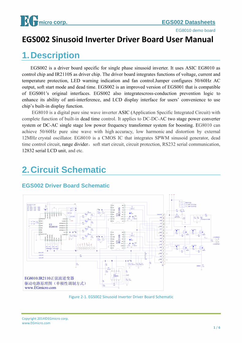
3. Pin
3.1 EG
3.2 Pin
Desig
1
2
3
4
5
6
7
8
9
1
icro corp
4©EGmicro corcom
ns and
GS002 Fr
n Descrip
gnator N
1 I
2 G
3 1
4 G
5 V
6 1
7 G
8 2
9 V
0 2
1. IFB
p.
rp.
d jump
ont View
Figu
ption
ame I/O
IFB I
GND GN
1LO O
GND GN
VS1 O
1HO O
GND GN
2LO O
VS2 O
2HO O
4. G
ND
3. 1
LO
2. G
ND
1.
IFB
pers
w
ure 3‐1. EGS0
O
I AC Outp
voltage i
ND Ground
O Right bri
ND Ground
O Right bri
O Right bri
ND Ground
O Left brid
O Left brid
O Left brid
7. G
ND
6. 1
HO
5. V
S1
02 Driver Boa
put Current Fe
s over 0.5V
idge low sidega
idge high side f
idge high side g
dge low side gat
dge high side flo
dge high side ga
11. G
ND
10. 2
HO
9. V
S2
8. 2
LO
ard Pin Defin
Des
eedback. Overc
ate drive output
floating supply r
gate drive outpu
te drive output
oating supply re
ate drive output
14. +5
V
13. G
ND
12. +1
5V
11
GND
*7. LED‐
EGS0
ition
scriptions
current protect
return
ut
eturn
17. FA
NCTR
16. TFB
15. V
FB
*6. LED+
*5. EN
*4. CLK
* 3DI
LCD Port
002 DataEG8010 de
tion turns on
3. DI
*2. GND
*1. +5V
asheetsemo board
2 / 6
when pin’s inp
6
put
micro corp. EGS002 Datasheets EG8010 demo board
Copyright 2014©EGmicro corp. www.EGmicro.com
3 / 6
11 GND GND Ground
12 +12V +12V +12V voltage input. (range: 10V-15V)
13 GND GND Ground
14 +5V +5V +5V power supply
15 VFB I AC Output voltage feedback. Referring to EG8010 datasheet for specific function and
circuit.
16 TFB I Temperature feedback. Overtemperature protection turns on when pin’s input voltage
is over 4.3V
17 FANCTR O
Connect to the fan control. When detects a temperature over 45, FANCTR
outputs high level “1” to turn on the fan. When the temperature is lower than 40,
FANCTR outputs low level “0” to turn off the fan.
* The followings are LCD display interface
*1 +5V +5V +5V power supply for the LCD
*2 GND GND Ground
*3 LCDDI I/O LCD Serial Data
*4 LCDCLK O LCD Serial Clock
*5 LCDEN O LCD Chip Select
*6 LED+ +5V +5V power supply for the backlight
*7 LED- GND Ground
3.3 Jumper settings
Designator Name Mark Setting Description
1 FS0 JP1 When JP1 is short, it selects AC output frequency at 60Hz
JP5 When JP5 is short, it selects AC output frequency at 50Hz
2 SST JP2 When JP2 is short, it enables 3 seconds soft start mode
JP6 When JP6 is short, it disables soft start mode
3 DT0 JP3 When JP7 and JP8 are short, dead time is 300ns.
When JP3 and JP8 are short, dead time is 500ns.
When JP4 and JP7 are short, dead time is 1.0us.
When JP3 and JP4 are short, dead time is 1.5us.
JP7
4 DT1 JP4
JP8
*5 LED+ JP9 When JP9 is short, LCD backlight is on
When JP9 is open, LCD backlight is off
The driver board’s jumperJP5, JP2, JP7 and JP8 are shorted as default setting, corresponding to 50Hz output, soft start mode on, 300nS dead time. Users can change these based on their needs. Warning: Jumper of the same function CANNOT be short circuited at the same time. (For example: JP1 And JP5 cannot be short at the same time.)

micro corp. EGS002 Datasheets EG8010 demo board
Copyright 2014©EGmicro corp. www.EGmicro.com
4 / 6
3.4 LED Warning Indication
EGS002 driver board provides LED warning indication function. User can determine problem according to the followings:
Normal:Lighting always on Overcurrent:Blink twice, off for 2 seconds, and keep cycling Overvoltage:Blink 3 times, off for 2 seconds, and keep cycling Undervoltage:Blink 4 times, off for 2 seconds, and keep cycling Overtemperature:Blink 5 times, off for 2 seconds, and keep cycling
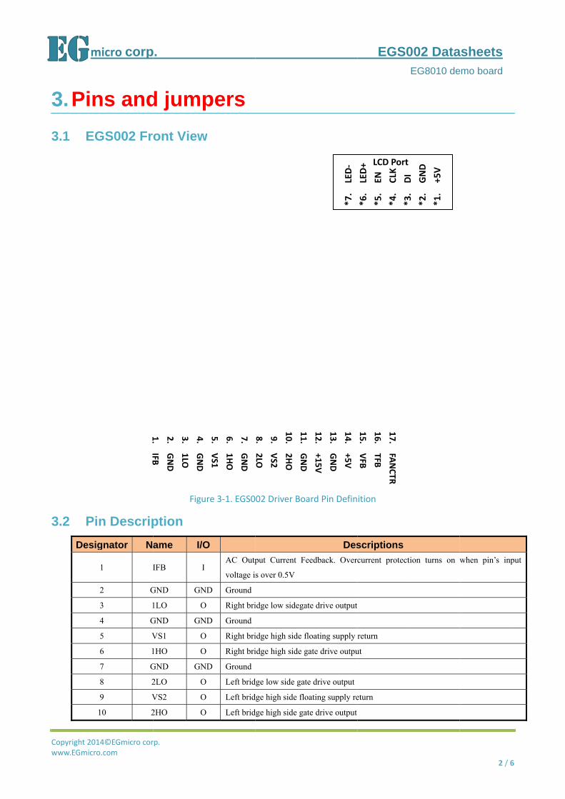
3.5 LCD Display Interface
EGS002 integrates LCD display interface for users’ convenience to test chip’s built-in display function that EG8010 supports.Shielding cable is required for connecting EGS002 driver board and LCD, otherwise inverter’s high voltage and high current environment will significantly interfere driver board’s operation.
EG8010 supports 12832 LCD (default) orLCD3220 thatwe specifically designed. Because two LCDs’ drivers are different, user has to specify if intends to buy LCD3220. Salesperson will ship 12832 LCD as default if not otherwise specified.
12832 LCD Connection Diagram:
Figure 3‐2. Connection betweenEGS002 and 12832 LCD Figure 3‐3. 12832 LCD Display
Note: There are many modules of LCD in the market. EG8010 supports majority of 12832 LCD based on control IC ST7920. Different LCDs may vary a little in pin map, name or description; user can obtain information online.
LCD3220 Connection Diagram:
*7. LED‐
*6. LED+
*5. EN
*4. CLK
*3. DI
*2. GND
*1. +5V
LED‐
LED+
CS
SCLK
SDI
VSS
VDD
LCD 12832
EGS002
mi
Copyright 2014www.EGmicro.
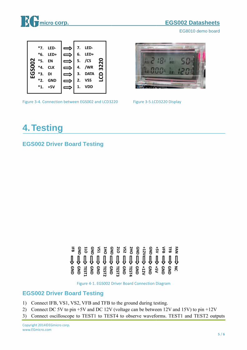
Figure 3‐4. C
4. Tes
EGS002
EGS002
1) Connec2) Connec3) Connec
*7.
*6.
*5.
*4.
*3.
*2.
*1.
EGS002
icro corp
4©EGmicro corcom
onnection be
sting
Driver B
Driver B
ct IFB, VS1ct DC 5V toct oscillosc
LED‐
LED+
EN
CLK
DI
GND
+5V
p.
rp.
etween EGS00
Board Te
Figure 4
Board Te
1, VS2, VFBo pin +5V aope to TES
1LO
GND
IFB
TEST1
GND
GND
7. LED
6. LED
5. /CS
4. /W
3. DA
2. VS
1. VD
02 and LCD32
esting
4‐1. EGS002 D
esting
B and TFB tand DC 12VST1 to TES
GND
1HO
VS1
GND
GND
TEST2
GND
GND
D‐
D+
S
WR
ATA
SS
DD
LCD 3220
220 F
Driver Board
to the grounV (voltage caST4 to obse
2HO
VS2
2LO
GND
TEST4
GND
TEST3
GND
Figure 3‐5.LC
Connection D
nd during tean be betweerve wavefo
+5V
GND
+12V
GND
+5V
GND
+12V
GND
EGS0
D3220 Displa
Diagram
esting. een 12V andorms. TEST
FAN
TFB
VFB
+5V
NC
GND
GND
+5V
002 DataEG8010 de
ay
d 15V) to piT1 and TES
asheetsemo board
5 / 6
in +12V ST2 outputs
6
s
micro corp. EGS002 Datasheets EG8010 demo board
Copyright 2014©EGmicro corp. www.EGmicro.com
6 / 6
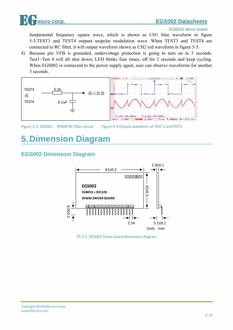
fundamental frequency square wave, which is shown as CH1 blue waveform in figure 5-3.TEST3 and TEST4 outputs unipolar modulation wave. When TEST3 and TEST4 are connected to RC filter, it will output waveform shown as CH2 red waveform in figure 5-3.
4) Because pin VFB is grounded, undervoltage protection is going to turn on in 3 seconds. Test1~Test 4 will all shut down; LED blinks four times, off for 2 seconds and keep cycling. When EGS002 is connected to the power supply again, user can observe waveforms for another 3 seconds.
Figure 4‐2. EGS002 SPWM RC filter circuit Figure 4‐3.Output waveform of TEST 2 andTEST3
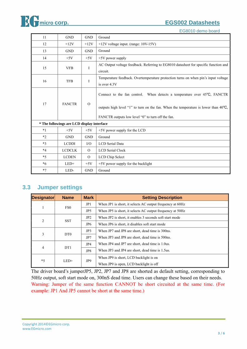
5. Dimension Diagram
EGS002 Dimension Diagram
图 5‐1. EGS002 Driver board dimension diagram
EGS002 EG8010 + R2110S
SPWM DRIVER BOARD
6.0±0.2
32±0.3
61±0.3 1.9±0.1
5.1±0.1 2.54
Unit:mm
TEST3
或
TEST4 0.1uF
接示波器 5.1k
Top Related