


Languages
Pages
Legal

ECS154BComputer Architecture
Designing a Multicycle Processor
Note Set 4
http://wwwcsif.cs.ucdavis.edu/~erciyes/154B

Recap: Processor Design is a Process
° Bottom-up• assemble components in target technology to establish critical
timing
° Top-down• specify component behavior from high-level requirements
° Iterative refinement• establish partial solution, expand and improve
datapath control
processorInstruction SetArchitecture
Reg. File Mux ALU Reg Mem Decoder Sequencer
Cells Gates

Recap: A Single Cycle Datapath
32
ALUctr
Clk
busW
RegWr
32
32
busA
32
busB
55 5
Rw Ra Rb
32 32-bitRegisters
Rs
Rt
Rt
RdRegDst
Exten
der
Mu
x
Mux
3216imm16
ALUSrc
ExtOp
Mu
x
MemtoReg
Clk
Data InWrEn
32
Adr
DataMemory
32
MemWr
AL
U
InstructionFetch Unit
Clk
Equal
Instruction<31:0>
0
1
0
1
01
<21:25>
<16:20>
<11:15>
<0:15>
Imm16RdRsRt
nPC_sel

Recap: The “Truth Table” for the Main Control
R-type ori lw sw beq jump
RegDst
ALUSrc
MemtoReg
RegWrite
MemWrite
Branch
Jump
ExtOp
ALUop (Symbolic)
1
0
0
1
0
0
0
x
“R-type”
0
1
0
1
0
0
0
0
Or
0
1
1
1
0
0
0
1
Add
x
1
x
0
1
0
0
1
Add
x
0
x
0
0
1
0
x
Subtract
x
x
x
0
0
0
1
x
xxx
op 00 0000 00 1101 10 0011 10 1011 00 0100 00 0010
ALUop <2> 1 0 0 0 0 x
ALUop <1> 0 1 0 0 0 x
ALUop <0> 0 0 0 0 1 x
MainControl
op
6
ALUControl(Local)
func
3
6
ALUop
ALUctr
3
RegDst
ALUSrc
:
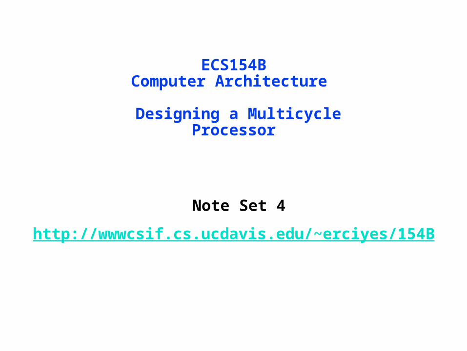
Recap: PLA Implementation of the Main Control
op<0>
op<5>. .op<5>. .<0>
op<5>. .<0>
op<5>. .<0>
op<5>. .<0>
op<5>. .<0>
R-type ori lw sw beq jumpRegWrite
ALUSrc
MemtoReg
MemWrite
Branch
Jump
RegDst
ExtOp
ALUop<2>
ALUop<1>
ALUop<0>

Recap: Systematic Generation of Control
° In our single-cycle processor, each instruction is realized by exactly one control command or “microinstruction”
• in general, the controller is a finite state machine
• microinstruction can also control sequencing (see later)
Control Logic / Store(PLA, ROM)
OPcode
Datapath
Inst
ruct
ion
Decode
Con
ditio
nsControlPoints
microinstruction

The Big Picture: Where are We Now?
° The Five Classic Components of a Computer
° Today’s Topic: Designing the Datapath for the Multiple Clock Cycle Datapath
Control
Datapath
Memory
Processor
Input
Output

Behavioral models of Datapath Componentsentity adder16 is
generic (ccOut_delay : TIME := 12 ns; adderOut_delay: TIME := 12 ns);port(A, B: in vlbit_1d(15 downto 0); DOUT: out vlbit_1d(15 downto 0); CIN: in vlbit; COUT: out vlbit);end adder16;
architecture behavior of adder32 isbegin
adder16_process: process(A, B, CIN)
variable tmp : vlbit_1d(18 downto 0);variable adder_out : vlbit_1d(31 downto 0);variable carry: vlbit;
begintmp := addum (addum (A, B), CIN);
adder_out := tmp(15 downto 0);carry :=tmp(16);
COUT <= carry after ccOut_delay; DOUT <= adder_out after adderOut_delay; end process;end behavior;
16
1616
A B
DOUT
CinCout

Behavioral Specification of Control Logic
° Decode / Control-store address modeled by Case statement
° Each arm of case drives control signals for that operation• just like the microinstruction
• either can be symbolic
entity maincontrol isport(opcode: in vlbit_1d(5 downto 0); equal_cond: in vlbit;
extop out vlbit;ALUsrc out vlbit;ALUop out vlbit_1d(1 downto 0);MEMwr out vlbit;MemtoReg out vlbit;RegWr out vlbit;RegDst out vlbit;nPC out vlbit;
end maincontrol;
architecture behavior of maincontrol isbegin control: process(opcode,equal_cond) constant ORIop: vlbit_ld(5 downto 0) := “001101”; begin -- extop only 0 (no extend) for ORI inst case opcode is
when ORIop => extop <= 0; when others => extop <= 1;end case;
end process;end behavior;
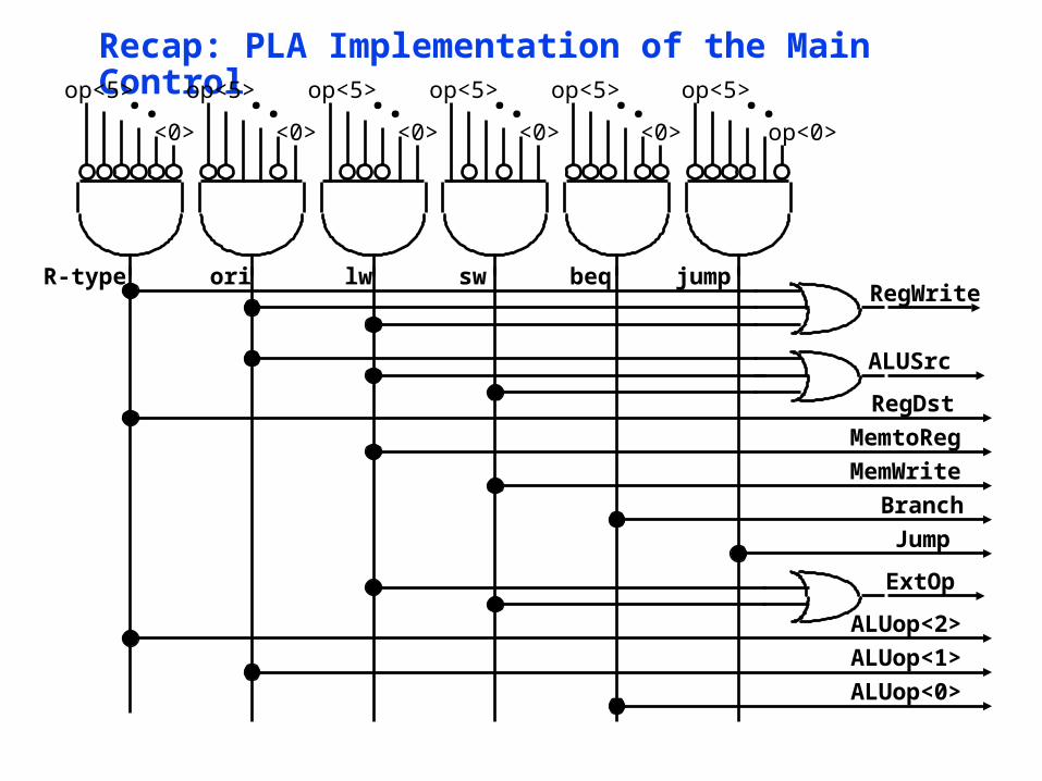
Abstract View of our single cycle processor
° looks like a FSM with PC as state
PC
Nex
t P
C
Reg
iste
rF
etch ALU Reg
. W
rt
Mem
Acc
ess
Dat
aM
emInst
ruct
ion
Fet
ch
Res
ult
Sto
re
AL
Uct
r
Reg
Dst
AL
US
rc
Ext
Op
Mem
Wr
Eq
ual
nPC
_sel
Reg
Wr
Mem
Wr
Mem
Rd
MainControl
ALUcontrol
op
fun
Ext

What’s wrong with our CPI=1 processor?
° Long Cycle Time
° All instructions take as much time as the slowest
° Real memory is not as nice as our idealized memory• cannot always get the job done in one (short) cycle
PC Inst Memory mux ALU Data Mem mux
PC Reg FileInst Memory mux ALU mux
PC Inst Memory mux ALU Data Mem
PC Inst Memory cmp mux
Reg File
Reg File
Reg File
Arithmetic & Logical
Load
Store
Branch
Critical Path
setup
setup

Memory Access Time
° Physics => fast memories are small (large memories are slow)
• question: register file vs. memory
° => Use a hierarchy of memories
Storage Array
selected word line
addressstorage cell
bit line
sense ampsaddressdecoder
CacheProcessor
1 time-period
proc
. bu
s
L2Cache
mem
. bu
s
2-3 time-periods20 - 50 time-periods
memory

Reducing Cycle Time
° Cut combinational dependency graph and insert register / latch
° Do same work in two fast cycles, rather than one slow one
° May be able to short-circuit path and remove some components for some instructions!
storage element
Acyclic CombinationalLogic
storage element
storage element
Acyclic CombinationalLogic (A)
storage element
storage element
Acyclic CombinationalLogic (B)

Basic Limits on Cycle Time
° Next address logic• PC <= branch ? PC + offset : PC + 4
° Instruction Fetch• InstructionReg <= Mem[PC]
° Register Access• A <= R[rs]
° ALU operation• R <= A + B
PC
Nex
t P
C
Ope
rand
Fet
ch Exec Reg
. F
ile
Mem
Acc
ess
Dat
aM
em
Inst
ruct
ion
Fet
ch
Res
ult
Sto
re
AL
Uct
r
Reg
Dst
AL
US
rc
Ext
Op
Mem
Wr
nPC
_sel
Reg
Wr
Mem
Wr
Mem
Rd
Control

Partitioning the CPI=1 Datapath
° Add registers between smallest steps
° Place enables on all registers
PC
Nex
t P
C
Ope
rand
Fet
ch Exec Reg
. F
ile
Mem
Acc
ess
Dat
aM
em
Inst
ruct
ion
Fet
ch
Res
ult
Sto
re
AL
Uct
r
Reg
Dst
AL
US
rc
Ext
Op
Mem
Wr
nPC
_sel
Reg
Wr
Mem
Wr
Mem
Rd
Equ
al

Example Multicycle Datapath
° Critical Path ?
PC
Nex
t P
C
Ope
rand
Fet
ch
Inst
ruct
ion
Fet
ch
nPC
_sel
IRRegFile E
xtA
LU Reg
. F
ile
Mem
Acc
ess
Dat
aM
em
Res
ult
Sto
reR
egD
stR
egW
r
Mem
Wr
Mem
Rd
S
M
Mem
ToR
eg
Equ
al
AL
Uct
rA
LU
Src
Ext
Op
A
B
E

Recall: Step-by-step Processor Design
Step 1: ISA => Logical Register Transfers
Step 2: Components of the Datapath
Step 3: RTL + Components => Datapath
Step 4: Datapath + Logical RTs => Physical RTs
Step 5: Physical RTs => Control

Step 4: R-rtype (add, sub, . . .)
° Logical Register Transfer
° Physical Register Transfers
inst Logical Register Transfers
ADDU R[rd] <– R[rs] + R[rt]; PC <– PC + 4
inst Physical Register Transfers
IR <– MEM[pc]
ADDU A<– R[rs]; B <– R[rt]
S <– A + B
R[rd] <– S; PC <– PC + 4
Exe
c
Reg
. F
ile
Mem
Acc
ess
Dat
aM
em
S
M
Reg
File
PC
Nex
t P
C
IR
Inst
. M
em
Tim
e
A
B
E

Step 4: Logical immed
° Logical Register Transfer
° Physical Register Transfers
inst Logical Register Transfers
ORI R[rt] <– R[rs] OR ZExt(Im16); PC <– PC + 4
inst Physical Register Transfers
IR <– MEM[pc]
ORI A<– R[rs]; B <– R[rt]
S <– A or ZExt(Im16)
R[rt] <– S; PC <– PC + 4
Exe
c
Reg
. F
ile
Mem
Acc
ess
Dat
aM
em
S
M
Reg
File
PC
Nex
t P
C
IR
Inst
. M
em
Tim
e
A
B
E

Step 4 : Load
° Logical Register Transfer
° Physical Register Transfers
inst Logical Register Transfers
LW R[rt] <– MEM[R[rs] + SExt(Im16)];
PC <– PC + 4
inst Physical Register Transfers
IR <– MEM[pc]
LW A<– R[rs]; B <– R[rt]
S <– A + SExt(Im16)
M <– MEM[S]
R[rd] <– M; PC <– PC + 4
Exe
c
Reg
. F
ile
Mem
Acc
ess
Dat
aM
em
S
M
Reg
File
PC
Nex
t P
C
IR
Inst
. M
em A
B
E
Tim
e

Step 4 : Store
° Logical Register Transfer
° Physical Register Transfers
inst Logical Register Transfers
SW MEM[R[rs] + SExt(Im16)] <– R[rt];
PC <– PC + 4
inst Physical Register Transfers
IR <– MEM[pc]
SW A<– R[rs]; B <– R[rt]
S <– A + SExt(Im16);
MEM[S] <– B PC <– PC + 4
Exe
c
Reg
. F
ile
Mem
Acc
ess
Dat
aM
em
S
M
Reg
File
PC
Nex
t P
C
IR
Inst
. M
em A
B
E
Tim
e

Step 4 : Branch° Logical Register Transfer
° Physical Register Transfers
inst Logical Register Transfers
BEQ if R[rs] == R[rt]
then PC <= PC + 4+SExt(Im16) || 00
else PC <= PC + 4
Exe
c
Reg
. F
ile
Mem
Acc
ess
Dat
aM
em
S
M
Reg
File
PC
Nex
t P
C
IR
Inst
. M
eminst Physical Register Transfers
IR <– MEM[pc]
BEQ E<– (R[rs] = R[rt])
if E then PC <– PC + 4 else PC <–PC+4+SExt(Im16)||00
A
B
ET
ime
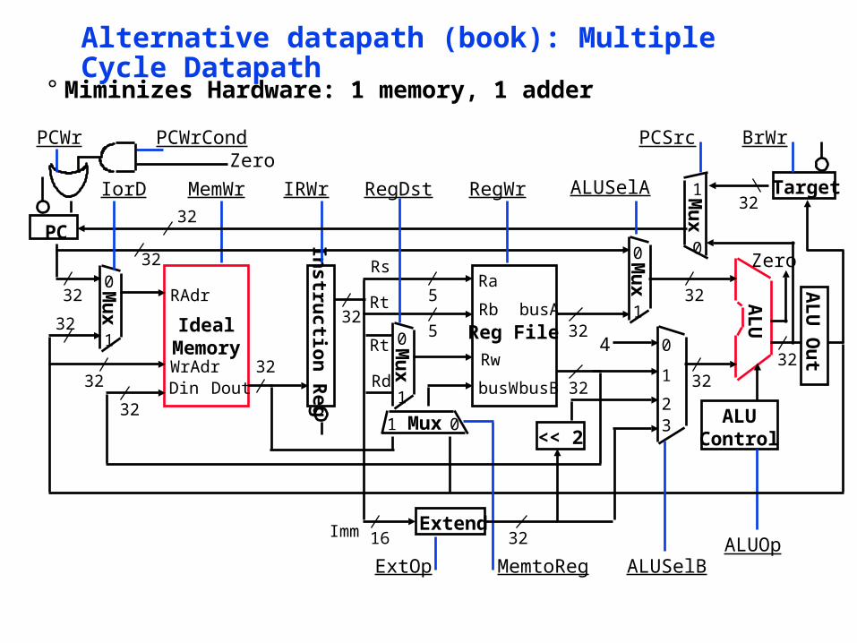
Alternative datapath (book): Multiple Cycle Datapath
° Miminizes Hardware: 1 memory, 1 adder
IdealMemoryWrAdrDin
RAdr
32
32
32Dout
MemWr
32
AL
U
3232
ALUOp
ALUControl
Instru
ction R
eg
32
IRWr
32
Reg File
Ra
Rw
busW
Rb5
5
32busA
32busB
RegWr
Rs
Rt
Mu
x
0
1
Rt
Rd
PCWr
ALUSelA
Mux 01
RegDst
Mu
x
0
1
32
PC
MemtoReg
Extend
ExtOp
Mu
x
0
132
0
1
23
4
16Imm 32
<< 2
ALUSelB
Mu
x1
0
Target32
Zero
ZeroPCWrCond PCSrc BrWr
32
IorD
AL
U O
ut

Our Control Model
° State specifies control points for Register Transfer
° Transfer occurs upon exiting state (same falling edge)
Control State
Next StateLogic
Output Logic
inputs (conditions)
outputs (control points)
State X
Register TransferControl Points
Depends on Input

Step 4 Control Specification for multicycle proc
IR <= MEM[PC]
R-type
A <= R[rs]B <= R[rt]
S <= A fun B
R[rd] <= SPC <= PC + 4
S <= A or ZX
R[rt] <= SPC <= PC + 4
ORi
S <= A + SX
R[rt] <= MPC <= PC + 4
M <= MEM[S]
LW
S <= A + SX
MEM[S] <= BPC <= PC + 4
BEQPC <= Next(PC,Equal)
SW
“instruction fetch”
“decode / operand fetch”
Exe
cute
Mem
ory
Writ
e-ba
ck
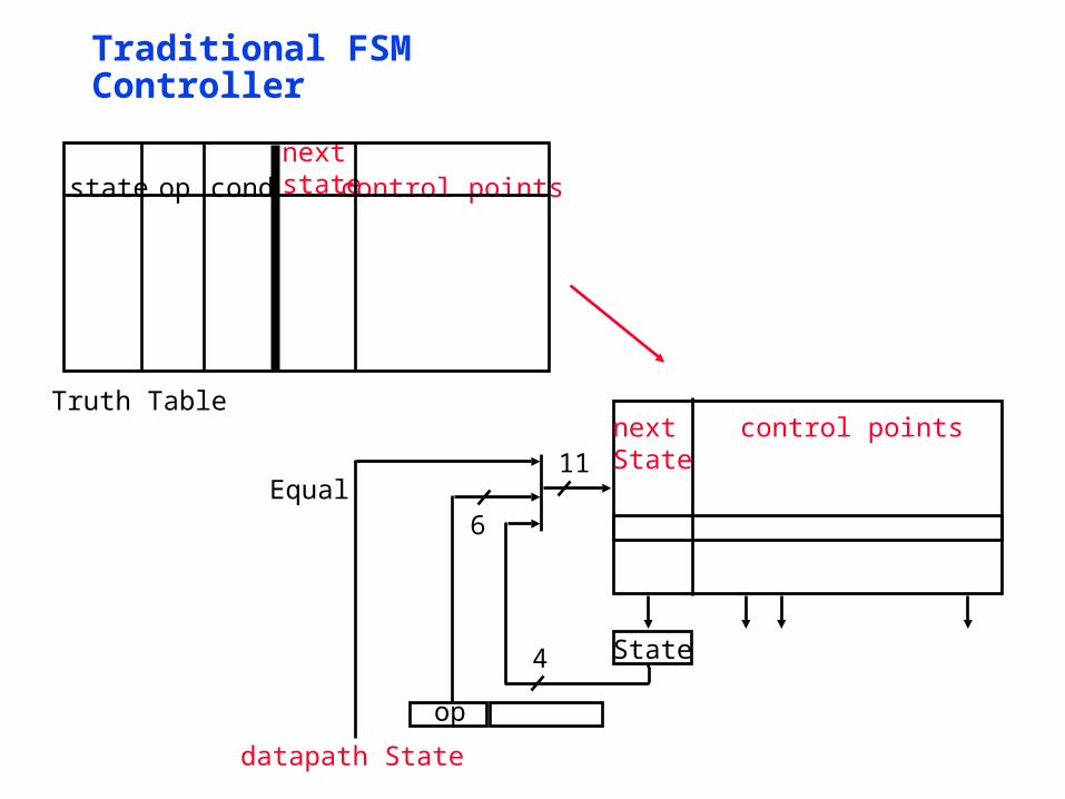
Traditional FSM Controller
State
6
4
11nextState
op
Equal
control points
state op condnextstate control points
Truth Table
datapath State
Step 5 (datapath + state diagram control)
° Translate RTs into control points
° Assign states
° Then go build the controller

Mapping RTs to Control Points
IR <= MEM[PC]
R-type
A <= R[rs]B <= R[rt]
S <= A fun B
R[rd] <= SPC <= PC + 4
S <= A or ZX
R[rt] <= SPC <= PC + 4
ORi
S <= A + SX
R[rt] <= MPC <= PC + 4
M <= MEM[S]
LW
S <= A + SX
MEM[S] <= BPC <= PC + 4
BEQ
PC <= Next(PC,Equal)
SW
“instruction fetch”
“decode”
imem_rd, IRen
ALUfun, Sen
RegDst, RegWr,PCen
Aen, Ben,Een
Exe
cute
Mem
ory
Writ
e-ba
ck
Assigning States
IR <= MEM[PC]
R-type
A <= R[rs]B <= R[rt]
S <= A fun B
R[rd] <= SPC <= PC + 4
S <= A or ZX
R[rt] <= SPC <= PC + 4
ORi
S <= A + SX
R[rt] <= MPC <= PC + 4
M <= MEM[S]
LW
S <= A + SX
MEM[S] <= BPC <= PC + 4
BEQ
PC <= Next(PC)
SW
“instruction fetch”
“decode”
0000
0001
0100
0101
0110
0111
1000
1001
1010
00111011
1100
Exe
cute
Mem
ory
Writ
e-ba
ck
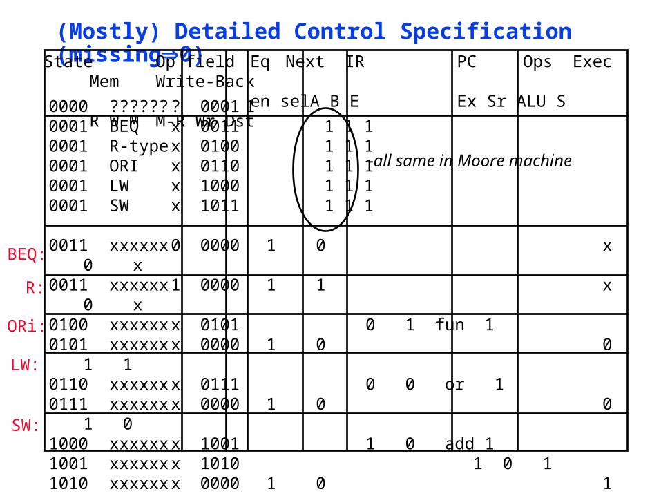
(Mostly) Detailed Control Specification (missing0)
0000 ?????? ? 0001 10001 BEQ x 0011 1 1 1 0001 R-type x 0100 1 1 1 0001 ORI x 0110 1 1 10001 LW x 1000 1 1 10001 SW x 1011 1 1 1
0011 xxxxxx 0 0000 1 0 x 0 x0011 xxxxxx 1 0000 1 1 x 0 x0100 xxxxxx x 0101 0 1 fun 10101 xxxxxx x 0000 1 0 0 1 10110 xxxxxx x 0111 0 0 or 10111 xxxxxx x 0000 1 0 0 1 01000 xxxxxx x 1001 1 0 add 11001 xxxxxx x 1010 1 0 11010 xxxxxx x 0000 1 0 1 1 01011 xxxxxx x 1100 1 0 add 11100 xxxxxx x 0000 1 0 0 1 0
State Op field Eq Next IR PC Ops Exec Mem Write-Backen sel A B E Ex Sr ALU S R W M M-R Wr Dst
R:
ORi:
LW:
SW:
-all same in Moore machine
BEQ:

Performance Evaluation
° What is the average CPI?• state diagram gives CPI for each instruction type
• workload gives frequency of each type
Type CPIi for type Frequency CPIi x freqIi
Arith/Logic 4 40% 1.6
Load 5 30% 1.5
Store 4 10% 0.4
branch 3 20% 0.6
Average CPI:4.1
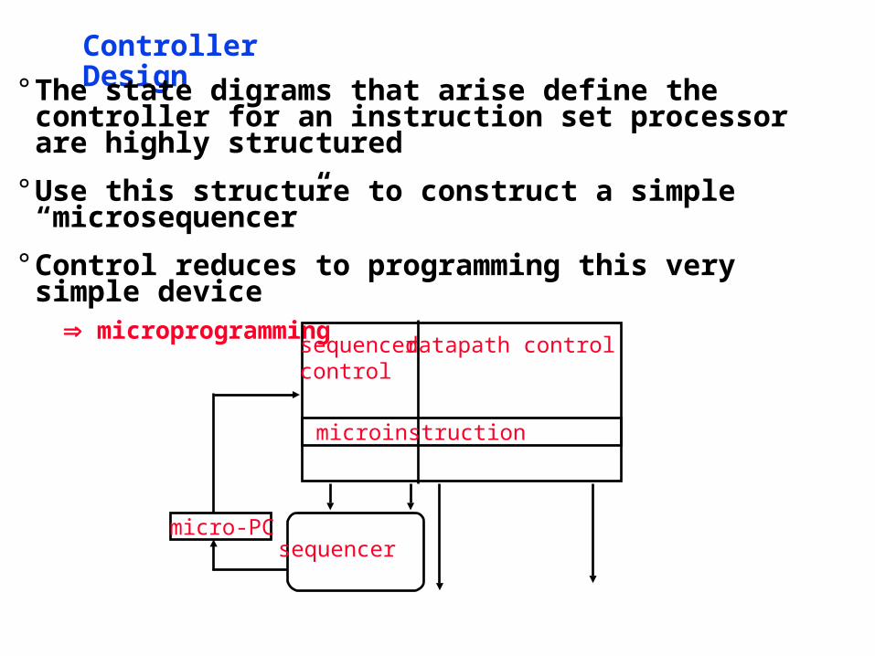
Controller Design° The state digrams that arise define the controller for an
instruction set processor are highly structured
° Use this structure to construct a simple “microsequencer”
° Control reduces to programming this very simple device microprogramming
sequencercontrol
datapath control
micro-PCsequencer
microinstruction

Example: Jump-Counter
op-codeMap ROM
Counterzeroincload
0000i
i+1
i
None of above: Do nothing (for wait states)

Using a Jump Counter
IR <= MEM[PC]
R-type
A <= R[rs]B <= R[rt]
S <= A fun B
R[rd] <= SPC <= PC + 4
S <= A or ZX
R[rt] <= SPC <= PC + 4
ORi
S <= A + SX
R[rt] <= MPC <= PC + 4
M <= MEM[S]
LW
S <= A + SX
MEM[S] <= BPC <= PC + 4
BEQ
PC <= Next(PC)
SW
“instruction fetch”
“decode”
0000
0001
0100
0101
0110
0111
1000
1001
1010
00111011
1100
inc
load
zero zerozero
zero
zeroinc inc inc inc
inc
Exe
cute
Mem
ory
Writ
e-ba
ck
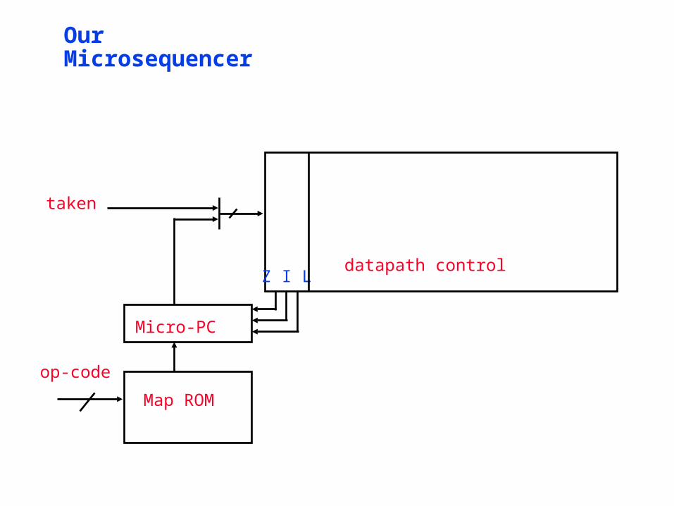
Our Microsequencer
op-code
Map ROM
Micro-PC
Z I Ldatapath control
taken
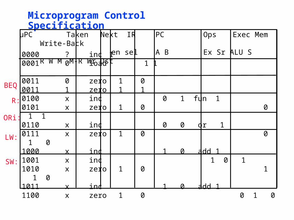
Microprogram Control Specification
0000 ? inc 10001 0 load 1 1
0011 0 zero 1 00011 1 zero 1 10100 x inc 0 1 fun 10101 x zero 1 0 0 1 10110 x inc 0 0 or 10111 x zero 1 0 0 1 01000 x inc 1 0 add 11001 x inc 1 0 11010 x zero 1 0 1 1 01011 x inc 1 0 add 11100 x zero 1 0 0 1 0
µPC Taken Next IR PC Ops Exec Mem Write-Backen sel A B Ex Sr ALU S R W M M-R Wr Dst
R:
ORi:
LW:
SW:
BEQ

Mapping ROM
R-type 000000 0100
BEQ 000100 0011
ori 001101 0110
LW 100011 1000
SW 101011 1011

Example: Controlling Memory
PC
InstructionMemory
Inst. Reg
addr
data
IR_en
InstMem_rd
IM_wait
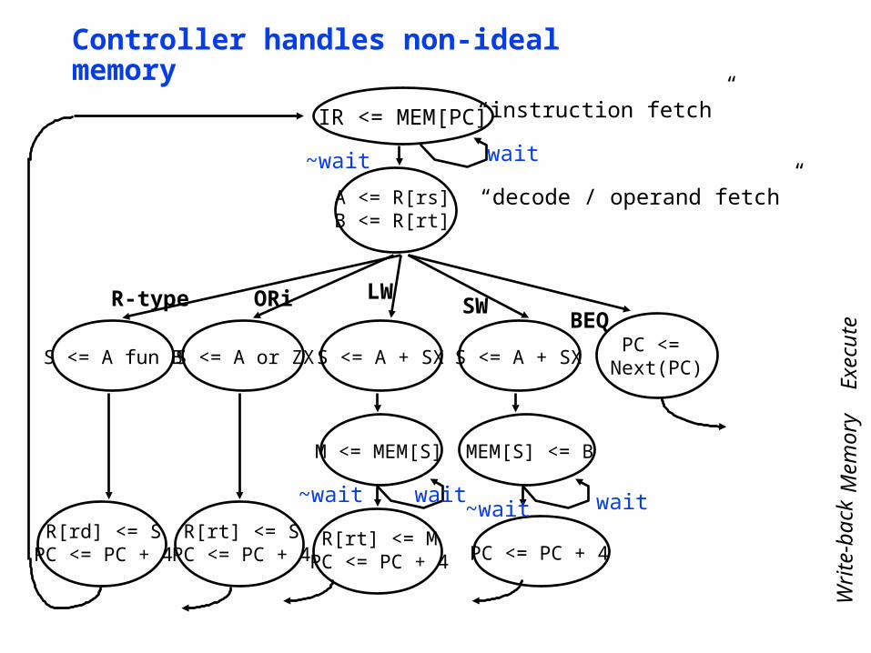
Controller handles non-ideal memory
IR <= MEM[PC]
R-type
A <= R[rs]B <= R[rt]
S <= A fun B
R[rd] <= SPC <= PC + 4
S <= A or ZX
R[rt] <= SPC <= PC + 4
ORi
S <= A + SX
R[rt] <= MPC <= PC + 4
M <= MEM[S]
LW
S <= A + SX
MEM[S] <= B
BEQPC <=
Next(PC)
SW
“instruction fetch”
“decode / operand fetch”
Exe
cute
Mem
ory
Writ
e-ba
ck
~wait wait
~wait wait
PC <= PC + 4
~wait wait

Really Simple Time-State Control
inst
ruct
ion
fet
chde
code
Exe
cute
Mem
ory
IR <= MEM[PC]
R-type
A <= R[rs]B <= R[rt]
S <= A fun B
R[rd] <= SPC <= PC + 4
S <= A or ZX
R[rt] <= SPC <= PC + 4
ORi
S <= A + SX
R[rt] <= MPC <= PC + 4
M <= MEM[S]
LW
S <= A + SX
MEM[S] <= B
BEQ
PC <= Next(PC)
SW
~wait wait
wait
PC <= PC + 4
wait
writ
e-ba
ck

Time-state Control Path
° Local decode and control at each stage
Exe
c
Reg
. F
ile
Mem
Acc
ess
Dat
aM
em
A
B
S
M
Reg
File
Equ
al
PC
Nex
t P
C
IR
Inst
. M
em
Valid
IRex
Dcd
Ctr
l
IRm
em
Ex
Ctr
l
IRw
b
Mem
Ctr
l
WB
Ctr
l

Overview of Control
° Control may be designed using one of several initial representations. The choice of sequence control, and how logic is represented, can then be determined independently; the control can then be implemented with one of several methods using a structured logic technique.
Initial Representation Finite State Diagram Microprogram
Sequencing Control Explicit Next State Microprogram counter Function + Dispatch ROMs
Logic Representation Logic Equations Truth Tables
Implementation PLA ROM Technique
“hardwired control” “microprogrammed control”

Summary
° Disadvantages of the Single Cycle Processor• Long cycle time
• Cycle time is too long for all instructions except the Load
° Multiple Cycle Processor:• Divide the instructions into smaller steps
• Execute each step (instead of the entire instruction) in one cycle
° Partition datapath into equal size chunks to minimize cycle time
• ~10 levels of logic between latches
° Follow same 5-step method for designing “real” processor

Summary (cont’d)° Control is specified by finite state digram
° Specialize state-diagrams easily captured by microsequencer
• simple increment & “branch” fields
• datapath control fields
° Control design reduces to Microprogramming
° Control is more complicated with:• complex instruction sets
• restricted datapaths (see the book)
° Simple Instruction set and powerful datapath simple control
• could try to reduce hardware (see the book)
• rather go for speed => many instructions at once!

Where to get more information?° Next two lectures:• Multiple Cycle Controller: Appendix C of your text book.
• Microprogramming: Section 5.5 of your text book.
° D. Patterson, “Microprograming,” Scientific American, March 1983.
° D. Patterson and D. Ditzel, “The Case for the Reduced Instruction Set Computer,” Computer Architecture News 8, 6 (October 15, 1980)
Top Related