


Languages
Pages
Legal


General DescriptionThe MAX8621Y/MAX8621Z power-management inte-grated circuits (PMICs) are designed for a variety ofportable devices including cellular handsets. ThesePMICs include two high-efficiency step-down DC-DCconverters, four low-dropout linear regulators (LDOs)with pin-programmable capability, one open-drain dri-ver, a 60ms (typ) reset timer, and power-on/off controllogic. These devices offer high efficiency with a no-loadsupply current of 160µA, and their small thin QFN 4mmx 4mm package makes them ideal for portable devices.
The step-down DC-DC converters utilize a proprietary4MHz hysteretic-PWM control scheme that allows forultra-small external components. Internal synchronousrectification improves efficiency and eliminates theexternal Schottky diode that is required in conventionalstep-down converters. The output voltage is adjustablefrom 0.6V to 3.3V. The output current is guaranteed upto 500mA.
The four LDOs offer low 45µVRMS output noise and lowdropout of only 100mV at 100mA. OUT1 and OUT2deliver 300mA (min) of continuous output current.OUT3 and OUT4 deliver 150mA (min) of continuousoutput current. The output voltages are pin selectableby SEL1 and SEL2 for flexibility. The MAX8621Y/MAX8621Z offer different sets of LDO output voltages.
A microprocessor reset output (RESET) monitors OUT1and warns the system of impending power loss, allow-ing safe shutdown. RESET asserts during power-up,power-down, shutdown, and fault conditions whereVOUT1 is below its regulation voltage.
A 200mA driver output is provided to control LED back-lighting or provide an open-drain connection for resis-tors such as in feedback networks.
ApplicationsCellular Handsets
Smart Phones, PDAs
Digital Cameras
MP3 Players
Wireless LAN
Features♦ Two 500mA Step-Down Converters
Up to 4MHz Switching FrequencyAdjustable Output from 0.6V to 3.3V
♦ Four Low-Noise LDOs with Pin-ProgrammableOutput Voltages
♦ One Open-Drain Driver
♦ 60ms (typ) Reset Timer
♦ Power-On/Off Control Logic and Sequencing
♦ 4mm x 4mm x 0.8mm 24-Pin Thin QFN
MA
X8
62
1Y
/MA
X8
62
1Z
Dual Step-Down DC-DC Power-Management ICs for Portable Devices
________________________________________________________________ Maxim Integrated Products 1
PART TEMP RANGE PIN-PACKAGE
MAX8621YETG -40°C to +85°C24 Thin QFN4mm x 4mm (T2444-4)
MAX8621ZETG -40°C to +85°C24 Thin QFN4mm x 4mm (T2444-4)
Ordering Information
MAX8621YMAX8621Z
IN1
IN2
IN3
PWRON
EN3
EN4
SEL2
ENDR
REFBP
GND
OUT1
OUT2
OUT3
OUT4
DR
LX1
FB1
PGND1
LX2
FB2
PGND2
RESET
SEL1
EN2
INPUT2.6V TO 5.5V
INPUT
OUT43V, 150mA
OUT31.8V, 150mA
OUT22.6V, 300mA
OUT12.6V, 300mA
BUCK11.375V, 500mA
BUCK21.8V, 500mA
RESET
Typical Operating Circuit
19-3539; Rev 0; 1/05
For pricing, delivery, and ordering information, please contact Maxim/Dallas Direct! at 1-888-629-4642, or visit Maxim’s website at www.maxim-ic.com.
Pin Configuration appears at end of data sheet.
EVALUATION KIT AVAILABLE
MA
X8
62
1Y
/MA
X8
62
1Z
Dual Step-Down DC-DC Power-Management ICs for Portable Devices
2 _______________________________________________________________________________________
ABSOLUTE MAXIMUM RATINGS
ELECTRICAL CHARACTERISTICS(VIN = 3.7V, CIN1 = 10µF, CIN2 = CIN3 = 4.7µF, COUT1 = COUT2 = 4.7µF, COUT3 = COUT4 = 2.2µF, CREFBP = 0.01µF, TA = -40°C to+85°C, unless otherwise noted. Typical values are at TA = +25°C.) (Notes 1, 2)
Stresses beyond those listed under “Absolute Maximum Ratings” may cause permanent damage to the device. These are stress ratings only, and functionaloperation of the device at these or any other conditions beyond those indicated in the operational sections of the specifications is not implied. Exposure toabsolute maximum rating conditions for extended periods may affect device reliability.
Note 1: LX_ has internal clamp diodes to GND and IN1. Applications that forward-bias these diodes should take care not to exceedthe IC’s package dissipation limits.
PWRON, IN1, IN2, IN3, RESET, FB1, FB2, ENDR, REFBP, SEL1, SEL2 to GND..................-0.3V to +6.0V
EN2, EN3, EN4, DR to GND.......................-0.3V to (VIN3 + 0.3V)OUT1, OUT2, OUT3, OUT4 to GND...........-0.3V to (VIN2 + 0.3V)PGND1, PGND2 to GND ......................................-0.3V to + 0.3VLX1, LX2 Current..........................................................±1.5ARMSLX1, LX2 to GND (Note 1) ..........................-0.3V to (VIN1 + 0.3V)DR Current......................................................................0.5ARMS
Continuous Power Dissipation (TA = +70°C)24-Pin 4mm x 4mm Thin QFN (derate 27.8mW/°C above +70°C)..........................2222.2mW
Operating Temperature Range ...........................-40°C to +85°CJunction Temperature ......................................................+150°CStorage Temperature Range .............................-65°C to +150°CLead Temperature (soldering, 10s) .................................+300°C
PARAMETER CONDITIONS MIN TYP MAX UNIT
Input Supply Range After startup 2.6 5.5 V
Shutdown Supply Current VIN = 4.2V (Note 3) 2 15 µA
VIN = 3.7V; BUCK1, BUCK2, OUT1, OUT2 on; othercircuits off
160 300No-Load Supply Current
VIN = 3.7V, BUCK1 and BUCK2 on, all LDOs on 275
µA
Light-Load Supply CurrentVIN = 3.7V, BUCK1 and BUCK2 with 500µA load each,OUT1 and OUT2 on, other circuits off
710 µA
UNDERVOLTAGE LOCKOUT
VIN rising 2.70 2.85 3.05Undervoltage Lockout (Note 4)
VIN falling 2.35 2.55V
THERMAL SHUTDOWN
Threshold TA rising +160 °C
Hysteresis 15 °C
REFERENCE
Reference Bypass OutputVoltage
TA = 0°C to +85°C 1.235 1.250 1.265 V
REF Supply Rejection 2.6V ≤ VIN ≤ 5.5V 0.2 mV/V
LOGIC AND CONTROL INPUTS
Input Low Level PWRON, EN2, EN3, EN4; 2.6V ≤ VIN ≤ 5.5V 0.4 V
PWRON, EN2, EN3, EN4; 2.6V ≤ VIN ≤ 4.2V 1.44 1.12Input High Level
PWRON, EN2, EN3, EN4; 2.6V ≤ VIN ≤ 5.5V 1.25V
Logic Input Current EN3, EN4; 0V < VIN < 5.5V -1 +1 µA
Tristate Low Input Threshold SEL_ 0.3 0.7 1.0 V
Tristate Low Input ThresholdHysteresis
SEL_ 50 mV
Tristate High Input Threshold SEL_VIN -1.2V
VIN -0.8V
VIN -0.4V
V

MA
X8
62
1Y
/MA
X8
62
1Z
Dual Step-Down DC-DC Power-Management ICs for Portable Devices
_______________________________________________________________________________________ 3
ELECTRICAL CHARACTERISTICS (continued)(VIN = 3.7V, CIN1 = 10µF, CIN2 = CIN3 = 4.7µF, COUT1 = COUT2 = 4.7µF, COUT3 = COUT4 = 2.2µF, CREFBP = 0.01µF, TA = -40°C to+85°C, unless otherwise noted. Typical values are at TA = +25°C.) (Notes 1, 2)
PARAMETER CONDITIONS MIN TYP MAX UNIT
Tristate High Input ThresholdHysteresis
SEL_ 50 mV
PWRON, EN2 Pulldown Resistorto GND
400 800 1600 kΩ
STEP-DOWN DC-DC CONVERTER 1 (BUCK1)
Supply Current ILOAD = 0A, no switching 40 µA
Output Voltage Range 0.6 3.3 V
FB1 Threshold Voltage VFB1 falling 0.603 V
FB1 Threshold Line Regulation 2.6V ≤ VIN ≤ 5.5V 0.3 %/V
FB1 Threshold Voltage Hysteresis(% of VFB1)
1 %
Shutdown 0.01FB1 Bias Current
VFB1 = 0.5V 0.01µA
p-MOSFET switch (ILIMP) 670 1000 1500Current Limit
n-MOSFET rectifier (ILIMN) 750 1000 1330mA
p-MOSFET switch, ILX1 = -40mA 0.65 1.5On-Resistance
n-MOSFET rectifier, ILX1 = 40mA 0.35 0.8Ω
Rectifier Off-Current Threshold ILXOFF 45 70 mA
tON 107Minimum On- and Off-Times
tOFF 95ns
STEP-DOWN DC-DC CONVERTER 2 (BUCK2)
Supply Current ILOAD = 0A, no switching 40 µA
Output Voltage Range 0.6 3.3 V
FB2 Threshold Voltage VFB2 falling 0.603 V
FB2 Threshold Line Regulation 2.6V ≤ VIN ≤ 5.5V 0.3 %/V
FB2 Threshold Voltage Accuracy(Falling) (% of VFB2)
ILOAD = 0A -2.5 +2.5 %
FB2 Threshold Voltage Hysteresis(% of VFB2)
1 %
Shutdown 0.01FB2 Bias Current
VFB = 0.5V 0.01µA
p-MOSFET switch 670 1000 1500Current Limit
n-MOSFET rectifier 750 1000 1330mA
p-MOSFET switch, ILX2 = -40mA 0.65 1.5On-Resistance
n-MOSFET rectifier, ILX2 = 40mA 0.35 0.8Ω
Rectifier Off-Current Threshold ILXOFF 45 70 mA
tON 107Minimum On- and Off-Times
tOFF 95ns

MA
X8
62
1Y
/MA
X8
62
1Z
Dual Step-Down DC-DC Power-Management ICs for Portable Devices
4 _______________________________________________________________________________________
ELECTRICAL CHARACTERISTICS (continued)(VIN = 3.7V, CIN1 = 10µF, CIN2 = CIN3 = 4.7µF, COUT1 = COUT2 = 4.7µF, COUT3 = COUT4 = 2.2µF, CREFBP = 0.01µF, TA = -40°C to+85°C, unless otherwise noted. Typical values are at TA = +25°C.) (Notes 1, 2)
PARAMETER CONDITIONS MIN TYP MAX UNIT
OUT1 (LDO1)
TA = 0°C to +85°C -1.3 +0.6 +2.0ILOAD = 1mA, 3.7V ≤ VIN ≤ 5.5V,relative to VOUT(NOM) TA = -40°C to +85°C -2.3 +2.5Output Voltage Accuracy
ILOAD = 150mA, relative to VOUT(NOM) 0
%
Output Current 300 mA
Current Limit VOUT1 = 0V 310 550 940 mA
Dropout Voltage ILOAD = 200mA, TA = +85°C 200 420 mV
Load RegulationVIN = greater of 3.7V or (VOUT(NOM) + 0.7V),1mA < ILOAD < 300mA, VSEL1 = VSEL2 = 0V
1.2 %
Power-Supply Rejection∆VOUT1/∆VIN2
10Hz to 10kHz, COUT1 = 4.7µF, ILOAD = 30mA 60 dB
Output Noise Voltage (RMS) 100Hz to 100kHz, COUT1 = 4.7µF, ILOAD = 30mA 45 µVRMS
0 < ILOAD < 300mA 4.7Output Capacitor for StableOperation 0 < ILOAD < 150mA 2.2
µF
Ground Current ILOAD = 500µA 21 µA
OUT2 (LDO2)
TA = 0°C to +85°C -1.3 +0.6 +2.0ILOAD = 1mA, 3.7V ≤ VIN_≤ 5.5V,relative to VOUT(NOM) TA = -40°C to +85°C -2.3 +2.5Output Voltage Accuracy
ILOAD = 150mA, relative to VOUT(NOM) 0
%
Output Current 300 mA
Current Limit VOUT2 = 0V 310 550 940 mA
Dropout Voltage ILOAD = 200mA , TA = +85°C 200 420 mV
Load Regulation 1mA < ILOAD < 300mA, VSEL1 = VSEL2 = 0V 1.2 %
Power-Supply Rejection∆VOUT2/∆VIN2
10Hz to 10kHz, COUT2 = 4.7µF, ILOAD = 30mA 60 dB
Output Noise Voltage (RMS) 100Hz to 100kHz, COUT2 = 4.7µF, ILOAD = 30mA 45 µVRMS
0 < ILOAD < 300mA 4.7Output Capacitor for StableOperation 0 < ILOAD < 150mA 2.2
µF
Ground Current ILOAD = 500µA 21 µA
OUT3 (LDO3)
TA = 0°C to +85°C -1.3 +0.3 +2.0ILOAD = 1mA, 3.7V ≤ VIN_ ≤ 5.5V,relative to VOUT(NOM) TA = -40°C to +85°C -2.3 +2.5Output Voltage Accuracy
ILOAD = 75mA, relative to VOUT(NOM) 0
%
Output Current 150 mA
Current Limit VOUT3 = 0V 165 360 650 mA
Dropout Voltage ILOAD = 100mA , TA = +85°C 100 210 mV
Load Regulation 1mA < ILOAD < 150mA, VSEL1 = VSEL2 = 0V 0.6 %

MA
X8
62
1Y
/MA
X8
62
1Z
Dual Step-Down DC-DC Power-Management ICs for Portable Devices
_______________________________________________________________________________________ 5
ELECTRICAL CHARACTERISTICS (continued)(VIN = 3.7V, CIN1 = 10µF, CIN2 = CIN3 = 4.7µF, COUT1 = COUT2 = 4.7µF, COUT3 = COUT4 = 2.2µF, CREFBP = 0.01µF, TA = -40°C to+85°C, unless otherwise noted. Typical values are at TA = +25°C.) (Notes 1, 2)
PARAMETER CONDITIONS MIN TYP MAX UNIT
Power-Supply Rejection∆VOUT3/∆VIN2
10Hz to 10kHz, COUT3 = 2.2µF, ILOAD = 30mA 60 dB
Output Noise Voltage (RMS) 100Hz to 100kHz, COUT3 = 2.2µF, ILOAD = 30mA 45 µVRMS
Output Capacitor for StableOperation
0 < ILOAD < 150mA 2.2 µF
OUT4 (LDO4)
VOUT(NOM) ≥ 1.8V -1.3 +0.3 +2.0TA = 0°C to+85°C VOUT(NOM) = 1.5V -1.30 +0.3 +2.35
ILOAD = 1mA, 3.7V ≤VIN_ ≤ 5.5V, relative toVOUT(NOM) TA = -40°C to +85°C -2.3 +2.5
Output Voltage Accuracy
ILOAD = 75mA, relative to VOUT(NOM) 0
%
Output Current 150 mA
Current Limit VOUT4 = 0V 165 360 650 mA
Dropout Voltage ILOAD = 100mA, TA = +85°C 100 210 mV
Load Regulation 1mA < ILOAD < 150mA, VSEL1 = VSEL2 = 0 0.6 %
Power-Supply Rejection∆VOUT4/∆VIN2
10Hz to 10kHz, COUT4 = 2.2µF, ILOAD = 30mA 60 dB
Output Noise Voltage (RMS) 100Hz to 100kHz, COUT4 = 2.2µF, ILOAD = 30mA 45 µVRMS
Output Capacitor for StableOperation
0 < ILOAD < 150mA 2.2 µF
DRIVER (DR)
ENDR Turn-On Threshold IDR = 1mA 0.65 V
ENDR Input Current VENDR = 0V and 5.5V -1 +1 µA
DR Output Low Voltage IDR = 150mA, VENDR = 3.7V 0.2 0.4 V
DR Off-Current (Leakage) VDR = VIN = 5.5V, VENDR = 0V -1 +1 µA
RESET
Output High VoltageVOUT1- 0.3V
V
Output Low Voltage ISINK = 1mA 0.3 V
RESET Threshold Percentage of nominal OUT1 rising when RESET falls 84 87 90 %
RESET Active Timeout Period From OUT1 ≥ 87% until RESET = HIGH 60 ms
Pullup Resistance to OUT1 8 14 20 kΩ
Note 1: VIN1, VIN2, and VIN3 are shorted together and single input is referred to as VIN.Note 2: All units are 100% production tested at TA = +85°C. Limits over the operating range are guaranteed by design.Note 3: OUT1, OUT2, OUT3, OUT4, LX1, and LX2 to ground.Note 4: When the input voltage is greater than 2.85V (typ), the UVLO comparator trips and the threshold is reduced to 2.35V (typ).
This allows the system to start normally until the input voltage decays to 2.35V.
MA
X8
62
1Y
/MA
X8
62
1Z
Dual Step-Down DC-DC Power-Management ICs for Portable Devices
6 _______________________________________________________________________________________
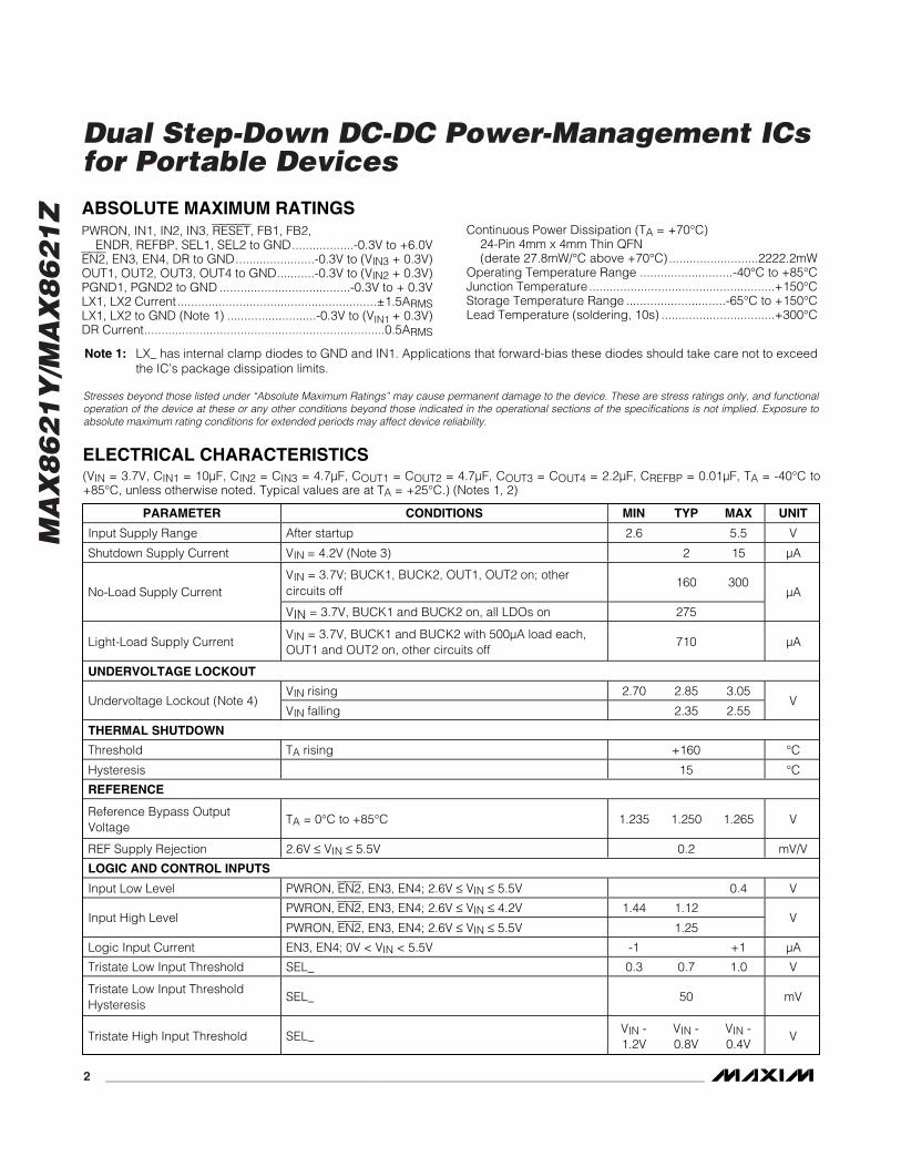
Typical Operating Characteristics(Circuit of Figure 3, VIN1 = VIN2 = VIN3 = 3.6V, PWRON = IN, VBUCK1 = 1.375V, VBUCK2 = 1.8V, VOUT1 = 2.6V, VOUT2 = 2.6V, VOUT3= 1.8V, VOUT4 = 3.0V, SEL1 = SEL2 = open, LX1 = LX2 = Murata LQH32CN2R2M53, TA = +25°C, unless otherwise noted.)
SUPPLY CURRENT vs. INPUT VOLTAGE
MAX
8621
toc0
1
INPUT VOLTAGE (V)
SUPP
LY C
URRE
NT (µ
A)
5.04.54.03.53.0
120
140
160
180
200
220
240
260
280
300
1002.5 5.5
NO LOADBUCK1, BUCK2, OUT1, OUT2: ON
STARTUP WAVEFORMSMAX8621 toc02
50µs/div
5V/div0
PWRON
BUCK1
BUCK2
OUT1
OUT2
2V/div02V/div0
5V/div0
5V/div0
SHUTDOWN WAVEFORMSMAX8621 toc03
100µs/div
5V/div0
PWRON
BUCK1
BUCK2
OUT1
OUT2
2V/div02V/div0
5V/div0
5V/div0
10mA LOAD ON ALL FOUR OUTPUTS
RESET WAVEFORMSMAX8621 toc04
20ms/div
2V/div0
PWRON
OUT1
RESET
2V/div
0
2V/div0
LOAD = 1mA
MA
X8
62
1Y
/MA
X8
62
1Z
Dual Step-Down DC-DC Power-Management ICs for Portable Devices
_______________________________________________________________________________________ 7
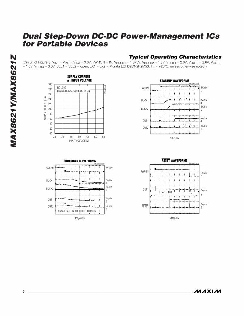
Typical Operating Characteristics (continued)(Circuit of Figure 3, VIN1 = VIN2 = VIN3 = 3.6V, PWRON = IN, VBUCK1 = 1.375V, VBUCK2 = 1.8V, VOUT1 = 2.6V, VOUT2 = 2.6V, VOUT3= 1.8V, VOUT4 = 3.0V, SEL1 = SEL2 = open, LX1 = LX2 = Murata LQH32CN2R2M53, TA = +25°C, unless otherwise noted.)
OUT1 OUPUT VOLTAGEvs. INPUT VOLTAGE
MAX
8621
toc0
5
INPUT VOLTAGE (V)
OUTP
UT V
OLTA
GE (V
)
5.04.54.03.53.0
2.525
2.550
2.575
2.600
2.625
2.650
2.5002.5 5.5
LOAD = 0
LOAD = 300mA
FALLING
RISING
OUT2 OUTPUT VOLTAGE ACCURACYvs. LOAD CURRENT
MAX
8621
toc0
6
LOAD CURRENT (mA)OU
TPUT
VOL
TAGE
ACC
URAC
Y (%
)25020050 100 150
-1.5
-1.0
-0.5
0
0.5
1.0
1.5
2.0
-2.00 300
OUT4 DROPOUT VOLTAGEvs. LOAD CURRENT
MAX
8621
toc0
7
LOAD CURRENT (mA)
DROP
OUT
VOLT
AGE
(mV)
10050
20
40
60
80
100
120
140
160
00 150
OUT1 POWER-SUPPLY RIPPLE REJECTION vs. FREQUENCY
MAX
8621
toc0
8
FREQUENCY (kHz)
POW
ER-S
UPPL
Y RI
PPLE
REJ
ECTI
ON (d
B)
100101
10
20
30
40
50
60
70
80
00.1 1000
EFFICICENCY vs. LOAD CURRENT(VBUCK2 = 1.8V)
MAX
8621
toc0
9
LOAD CURRENT (mA)
EFFI
CIEN
CY (%
)
100101
50
60
70
80
90
100
400.1 1000
2.2µH4.7µH
1µH
BUCK1, OUT1, OUT2:ON WITH NO LOAD
EFFICICENCY vs. LOAD CURRENT(VBUCK1 = 1.375V)
MAX
8621
toc1
0
LOAD CURRENT (mA)
EFFI
CIEN
CY (%
)
100101
50
60
70
80
90
100
400.1 1000
2.2µH 4.7µH
1µH
BUCK2, OUT1, OUT2:ON WITH NO LOAD

MA
X8
62
1Y
/MA
X8
62
1Z
Dual Step-Down DC-DC Power-Management ICs for Portable Devices
8 _______________________________________________________________________________________
SWITCHING FREQUENCY vs. LOAD CURRENT
MAX
8621
toc1
1
LOAD CURRENT (mA)
FREQ
UENC
Y (M
Hz)
100 200 300 400
1
10
0.10 500
1µH
2.2µH
4.7µH
BUCK1 OUTPUT VOLTAGEvs. LOAD CURRENT (VOLTAGE POSITIONING)
MAX
8621
toc1
5
LOAD CURRENT (mA)
OUTP
UT V
OLTA
GE (V
)
400300200100
1.32
1.34
1.36
1.38
1.40
1.42
1.44
1.300 500
BUCK1 LIGHT-LOAD WAVEFORMSMAX8621 toc12
200ns/div
10mV/divAC-COUPLED
VBUCK1
ILX1
VLX1
200mA/div
0
5V/div0
LOAD = 50mA
BUCK1 LOAD-TRANSIENT RESPONSEMAX8621 toc14
5µs/div
50mV/divAC-COUPLED
VBUCK1
ILX1
IBUCK1
500mA/div0
500mA/div0
400mA LOAD
BUCK1 HEAVY-LOAD WAVEFORMSMAX8621 toc13
200ns/div
10mV/divAC-COUPLED
VBUCK1
ILX1
VLX1
200mA/div
0
5V/div0
LOAD = 300mA
Typical Operating Characteristics (continued)(Circuit of Figure 3, VIN1 = VIN2 = VIN3 = 3.6V, PWRON = IN, VBUCK1 = 1.375V, VBUCK2 = 1.8V, VOUT1 = 2.6V, VOUT2 = 2.6V, VOUT3= 1.8V, VOUT4 = 3.0V, SEL1 = SEL2 = open, LX1 = LX2 = Murata LQH32CN2R2M53, TA = +25°C, unless otherwise noted.)

MA
X8
62
1Y
/MA
X8
62
1Z
Dual Step-Down DC-DC Power-Management ICs for Portable Devices
_______________________________________________________________________________________ 9
Pin Description
PIN NAME FUNCTION
1 FB1 Voltage Feedback for Step-Down Converter 1. FB1 regulates to 0.6V nominal.
2 FB2 Voltage Feedback for Step-Down Converter 2. FB2 regulates to 0.6V nominal.
3 GND Ground. Ground for all LDOs and the control section.
4 REFBPReference Noise Bypass. Connect a 0.01µF ceramic capacitor from REFBP to GND. Not intended to drive resistiveload. REFBP is high impedance in shutdown.
5 EN4 Enable Input for OUT4. Drive EN4 high to turn on OUT4.
6 OUT4150mA LDO4 output. Bypass OUT4 to GND with a 2.2µF ceramic capacitor. OUT4 is high impedance whendisabled. OUT4 can only be activated if OUT1 is within 87% of regulation.
7 EN3 Enable Input for OUT3. Drive EN3 high to turn on OUT3.
8 EN2Enable Input for OUT2. Drive EN2 high to disable OUT2. Drive EN2 low or leave open to enable OUT2. EN2 isinternally pulled to GND by an 800kΩ (typ) pulldown resistor. If the MAX8621Y/MAX8621Z are placed into shutdownusing PWRON (PWRON = low), OUT2 does not power regardless of the status of EN2.
9 OUT2300mA LDO2 Output. Bypass with a 4.7µF ceramic capacitor to GND. OUT2 is high impedance when disabled.OUT2 can only be activated if OUT1 is within 87% of regulation.
10 IN2Supply Voltage to the Output MOSFET of All 4 LDOs. IN2 must be shorted to IN1 and IN3. Connect a 4.7µF ceramiccapacitor from IN2 to GND.
11 RESETOpen-Drain, Active-Low Reset Output. RESET asserts low when VOUT1 drops below 87% (typ) of regulation. RESETdeasserts 60ms after VOUT1 rises above 87% (typ) of regulation (Figure 2).
12 OUT1 300m A LD O1 O utp ut. Byp ass w i th a 4.7µF cer am i c cap aci tor to G N D . OU T1 i s hi g h i m p ed ance w hen d i sab l ed .
13 OUT3150mA LDO3 Output. Bypass OUT3 to GND with a 2.2µF ceramic capacitor. OUT3 is high impedance whendisabled. OUT3 can only be activated if OUT1 is within 87% of regulation.
14 PWRONPower Enable Input. Drive PWRON high to enable the MAX8621Y/MAX8621Z. Drive PWRON low to enter shutdownmode. PWRON has an internal 800kΩ (typ) pulldown resistor.
15 ENDREnable Input for DR. Drive ENDR low for DR to go into high impedance. Drive ENDR high to activate DR, pullingDR low.
16 IN3Supply Voltage to the Control Section. IN3 must be shorted to IN1 and IN2. Connect a 4.7µF ceramic capacitor fromIN3 to GND.
17 SEL2LDO Output-Voltage Select Input 2. SEL1 and SEL2 set the OUT1, OUT2, OUT3, and OUT4 voltages to one of ninecombinations (Table 1).
18 SEL1LDO Output-Voltage Select Input 1. SEL1 and SEL2 set the OUT1, OUT2, OUT3, and OUT4 voltages to one of ninecombinations (Table 1).
19 DR200mA Driver Output. Connects to the open drain of an internal n-channel MOSFET whose gate is controlled byENDR.
20 PGND2 Power Ground for BUCK2 and DR Switch
21 LX2Inductor Connection for BUCK2. LX2 is internally connected to the drain of the internal p-channel MOSFET and thedrain of the internal n-channel synchronous rectifier for BUCK2. LX2 is high impedance when BUCK2 is disabled.
22 IN1Supply Voltage to the Output Stage of BUCK1 and BUCK2. IN1 must be shorted to IN2 and IN3. Connect a 10µFceramic capacitor from IN1 to GND.
23 LX1Inductor Connection for BUCK1. LX1 is internally connected to the drain of the internal p-channel MOSFET and thedrain of the internal n-channel synchronous rectifier for BUCK1. LX1 is high impedance when BUCK1 is disabled.
24 PGND1 Power Ground for BUCK1
— EP Exposed Paddle. Connect the exposed paddle to GND, PGND1, and PGND2.

MA
X8
62
1Y
/MA
X8
62
1Z
Dual Step-Down DC-DC Power-Management ICs for Portable Devices
10 ______________________________________________________________________________________
Detailed DescriptionThe MAX8621Y/MAX8621Z power-management ICs aredesigned specifically to power a variety of portabledevices including cellular handsets. Each device con-tains two 4MHz high-efficient step-down converters, fourlow-dropout linear regulators (LDOs), a 60ms (typ) resettimer, a 200mA open-drain output driver, and power-on/off control logic (Figure 3).
Step Down DC-DC Control SchemeThe MAX8621Y/MAX8621Z step-down converters areoptimized for high-efficiency voltage conversion over awide load range, while maintaining excellent transientresponse, minimizing external component size, andminimizing output voltage ripple. The DC-DC convert-ers (BUCK1 and BUCK2) also feature an optimized on-resistance internal MOSFET switch and synchronousrectifier to maximize efficiency. The MAX8621Y/MAX8621Z utilize a proprietary hysteretic-PWM controlscheme that switches with nearly fixed frequency up to4MHz, allowing for ultra-small external components.The step-down converter output current is guaranteedup to 500mA, while consuming 40µA (typ).
When the step-down converter output voltage falls belowthe regulation threshold, the error comparator begins aswitching cycle by turning the high-side p-channel MOSFET switch on. This switch remains on until the mini-mum on-time (tON) expires and the output voltage is inregulation or the current-limit threshold (ILIMP) is exceed-ed. Once off, the high-side switch remains off until theminimum off-time (tOFF) expires and the output voltageagain falls below the regulation threshold. During this offperiod, the low-side synchronous rectifier turns on andremains on until either the high-side switch turns on orthe inductor current reduces to the rectifier-off currentthreshold (ILXOFF = 45mA (typ)). The internal synchro-nous rectifier eliminates the need for an externalSchottky diode.
Voltage-Positioning Load RegulationThe MAX8621Y/MAX8621Z use a unique step-downconverter feedback network. By taking feedback fromthe LX node through R1, the usual phase lag due to theoutput capacitor is removed, making the loop exceed-ingly stable and allowing the use of a very small ceramicoutput capacitor. This configuration causes the outputvoltage to shift by the inductor series resistance multi-plied by the load current. This output voltage shift isknown as voltage-positioning load regulation. Voltage-positioning load regulation greatly reduces overshootduring load transients, which effectively halves thepeak-to-peak output-voltage excursions compared totraditional step-down converters. See the Buck1 Load-
Transient Response graph in the Typical OperatingCharacteristics.
Low-Dropout Linear RegulatorsEach MAX8621Y/MAX8621Z contains four low-dropout,low-quiescent-current, high-accuracy linear regulators(LDOs). OUT1 and OUT2 supply loads up to 300mA,while OUT3 and OUT4 supply loads up to 150mA. TheLDO output voltages are set using SEL1 and SEL2 (seeTable 1). The LDOs include an internal reference, erroramplifier, p-channel pass transistor, internal program-mable voltage-divider, and an OUT1 power-good com-parator. Each error amplifier compares the referencevoltage to a feedback voltage and amplifies the differ-ence. If the feedback voltage is lower than the refer-ence voltage, the pass-transistor gate is pulled lower,allowing more current to pass to the outputs andincreasing the output voltage. If the feedback voltage istoo high, the pass-transistor gate is pulled up, allowingless current to pass to the output.
DR DriverEach MAX8621Y/MAX8621Z includes a 1.3Ω n-channelMOSFET open-drain output that is controlled by ENDR.This output can be used to drive LEDs (see the TypicalOperating Circuit) and allow adjustable output voltages(see Figure 1).
Programming LDO Output Voltages (SEL1, SEL2)
As shown in Table 1, the LDO output voltages, OUT1,OUT2, OUT3, and OUT4 are pin-programmable by thelogic states of SEL1 and SEL2. SEL1 and SEL2 aretrilevel inputs: IN, open, and GND. The input voltage,VIN, must be greater than the selected OUT1, OUT2,OUT3, and OUT4 voltages. The logic states of SEL1and SEL2 can be programmed only during power-up.Once the OUT_ voltages are programmed, their valuesdo not change by changing SEL_ unless theMAX8621Y/MAX8621Z power is cycled.
MAX8621YMAX8621Z
L12.2µH
C6150pF
R2115kΩ
R1150kΩ
R5215kΩ
DR
FB1
LX1
BUCK11.38V OR 1.8V
ENDR1.38/1.8
Figure 1. Adjusting BUCK1 Output Voltage Using DR

Power-Supply SequenceBUCK1 is always first on and last off in the MAX8621Y/MAX8621Zs’ power sequence. BUCK1 turns on approxi-mately 40µs after PWRON is enabled. BUCK2 turns onapproximately 40µs after BUCK1, and OUT1 turns on65µs after BUCK2. These delays have been added tosequence the turn-on of the step-down converters andLDOs so that the initial current surges are distributed
over time. For the same reason, OUT2, OUT3, and OUT4can be turned on by EN2, EN3, and EN4 signals, butonly after OUT1 has reached 87% of its final value. Notethat OUT2 typically requires a longer time to enable thanOUT3 and OUT4 (45µs versus 15µs). All regulators canbe turned off at the same time when PWRON is low, butBUCK1 remains on for approximately another 120µsafter PWRON goes low.
MA
X8
62
1Y
/MA
X8
62
1Z
Dual Step-Down DC-DC Power-Management ICs for Portable Devices
______________________________________________________________________________________ 11
MAX8621Y MAX8621ZSEL1 SEL2
OUT1 (V) OUT2 (V) OUT3 (V) OUT4 (V) OUT1 (V) OUT2 (V) OUT3 (V) OUT4 (V)
IN IN 3.3 3.3 2.85 2.85 2.8 2.6 3.0 3.0
IN OPEN 3.0 3.3 3.3 2.85 2.6 2.6 3.0 3.0
IN GND 2.5 3.3 2.85 3.0 2.6 2.6 2.9 2.9
OPEN IN 2.85 3.3 3.0 2.5 2.6 2.6 3.0 3.3
OPEN OPEN 3.3 3.3 2.8 3.0 2.6 2.6 1.8 3.0
OPEN GND 3.3 3.3 3.0 3.0 2.6 2.6 2.8 3.0
GND IN 3.3 2.85 3.3 2.85 2.9 3.1 1.8 1.5
GND OPEN 2.85 2.85 3.3 3.3 3.0 2.9 2.9 2.9
GND GND 3.3 2.85 3.0 3.0 3.0 2.5 2.9 2.9
Table 1. SEL1 and SEL2, MAX8621Y/MAX8621Z Output Voltage Selection
PWRON
BUCK2
OUT1
BUCK1
REF
EN2
OUT3(OUT4)
EN3(EN4)
OUT2
RESET
15µs
65µs
40µs
87% REGULATION
87% REGULATION
60ms
45µs
120µs
40µs
Figure 2. Power-On/Off Sequence Diagram

MA
X8
62
1Y
/MA
X8
62
1Z PWRON
Drive PWRON low or leave PWRON open to place theMAX8621Y/MAX8621Z in power-down mode andreduce supply current to 5µA (typ). In power-down, thecontrol circuitry, internal-switching p-channel MOSFET,and the internal synchronous rectifier (n-channel MOSFET) turn off (BUCK1 and BUCK2), and LX_becomes high impedance. In addition, all four LDOsare disabled. Connect PWRON to IN or logic-high toenable the MAX8621Y/MAX8621Z. EN2 enables anddisables OUT2 when PWRON is high.
OUT2 Enable (EN2)Drive EN2 high to disable OUT2. Drive EN2 low orleave open to enable OUT2. EN2 is internally pulled toGND by an 800kΩ (typ) pulldown resistor. If theMAX8621Y/MAX8621Z are powered down usingPWRON (PWRON = low), OUT2 does not powerregardless of the status of EN2.
Reset Output (RESET)The reset circuit is active both at power-up and power-down. RESET asserts low when VOUT1 drops below87% (typ) of regulation. RESET deasserts 60ms afterVOUT1 rises above 87% (typ) of regulation. RESET ispulled up through an internal 14kΩ resistor to OUT1.
Undervoltage LockoutInitial power-up of the MAX8621Y/MAX8621Z occurswhen VIN is greater than 2.85V (typ) and PWRONasserts. Once VIN exceeds 2.85V (typ), the undervolt-age lockout has 0.5V of hysteresis, allowing the VINoperating range to drop down to 2.35V (typ) withoutshutting down.
Current LimitingThe MAX8621Y/MAX8621Z OUT1 and OUT2 LDOs limittheir output current to 550mA (typ). OUT3 and OUT4LDOs limit their output current to 360mA (typ). If the LDOoutput current exceeds the current limit, the correspond-ing LDO output voltage drops. The step-down converters(BUCK1 and BUCK2) limit the p-channel MOSFET to670mA (min) and the n-channel MOSFET to 750mA (min).
Reference Bypass Capacitor Node (REFBP)
An external 0.01µF bypass capacitor and an internal100kΩ (typ) resistor at REFBP create a lowpass filter forLDO noise reduction. OUT1, OUT2, OUT3, and OUT4exhibit 45µVRMS of output voltage noise with CREFBP =0.01µF, COUT1 = COUT2 = 4.7µF, and COUT3 = COUT4= 2.2µF.
Thermal-Overload ProtectionThermal-overload protection limits total power dissipa-tion in the MAX8621Y/MAX8621Z. Independent thermal-protection circuits monitor the step-down convertersand the linear-regulator circuits. When the junction tem-perature exceeds TJ = +160°C, the thermal-overloadprotection circuit disables the corresponding circuitry,allowing the IC to cool. The LDO thermal-overload pro-tection circuit enables the LDOs after the LDO junctiontemperature cools down, resulting in pulsed LDO out-puts during continuous thermal-overload conditions. Thestep-down converter’s thermal-overload protection circuitry enables the step-down converter after thejunction temperature cools down. Thermal-overloadprotection safeguards the MAX8621Y/MAX8621Z in theevent of fault conditions. For continuous operation, donot exceed the absolute maximum junction-temperaturerating of TJ = +150°C.
Applications InformationStep-Down DC-DC Converter
Setting the Step-Down Output VoltageSelect an output voltage for BUCK1 between 0.6V and3.3V by connecting FB1 to a resistive voltage-dividerbetween LX1 and GND. Choose R2 (Figure 3) for a rea-sonable bias current in the resistive divider. A wide rangeof resistor values is acceptable, but a good starting pointis to choose R2 as 100kΩ. Then, R1 (Figure 3) is given by:
where VFB = 0.6V. For BUCK2, R3 and R4 are calculatedusing the same methods.
Input CapacitorThe input capacitor, CIN1, reduces the current peaksdrawn from the battery or input power source andreduces switching noise in the IC. The impedance ofCIN1 at the switching frequency should be kept verylow. Ceramic capacitors with X5R or X7R dielectrics arehighly recommended due to their small size, low ESR,and small temperature coefficients. Due to theMAX8621Y/MAX8621Z step-down converter’s fast soft-start, the input capacitance can be very low. Use a10µF ceramic capacitor or an equivalent amount ofmultiple capacitors in parallel between IN1 and ground.Connect CIN1 as close to the IC as possible to minimizethe impact of PC board trace inductance. Use a 4.7µFceramic capacitor from IN2 to ground and a second4.7µF ceramic capacitor from IN3 to ground.
R RVVOUT
FB1 2 1=
⎛⎝⎜
⎞⎠⎟
−
Dual Step-Down DC-DC Power-Management ICs for Portable Devices
12 ______________________________________________________________________________________

Inductor SelectionThe MAX8621Y/MAX8621Z step-down converters oper-ate with inductors between 1µH and 4.7µH. Low-induc-tance values are physically smaller but require fasterswitching, resulting in some efficiency loss. See theTypical Operating Characteristics for efficiency andswitching frequency vs. inductor value plots. Theinductor’s DC current rating needs to be only 100mAgreater than the application’s maximum load currentbecause the step-down converter features zero-currentovershoot during startup and load transients.
For output voltages above 2.0V, when light-load effi-ciency is important, the minimum recommended induc-tor is 2.2µH. For optimum voltage-positioning loadtransients, choose an inductor with DC series resis-tance in the 50mΩ to 150mΩ range. For higher efficien-cy at heavy loads (above 200mA) or minimal loadregulation (but some transient overshoot), the resis-tance should be kept below 100mΩ. For light-loadapplications up to 200mA, much higher resistance isacceptable with very little impact on performance. SeeTable 2 for some suggested inductors.
MA
X8
62
1Y
/MA
X8
62
1Z
Dual Step-Down DC-DC Power-Management ICs for Portable Devices
______________________________________________________________________________________ 13
MANUFACTURER SERIESINDUCTANCE
(µH)ESR(Ω)
CURRENT RATING(mA)
DIMENSIONS
CB20122.24.7
0.230.40
410300
2.0 x 1.25 x 1.25= 3.1mm3
LB20121.02.2
0.150.23
300240
2.0 x 1.25 x 1.25= 3.1mm3
LB2016
1.01.52.23.3
0.090.110.130.20
455350315280
2.0 x 1.6 x 1.8= 5.8mm3
LB2518
1.01.52.23.3
0.060.070.090.11
500400340270
2.5 x 1.8 x 2.0= 9mm3
Taiyo Yuden
LBC2518
1.01.52.23.34.7
0.080.110.130.160.20
775660600500430
2.5 x 1.8 x 2.0= 9mm3
LQH32C_531.02.24.7
0.060.100.15
1000790650
3.2 x 2.5 x 1.7= 14mm3
Murata
LQM43FN2.24.7
0.100.17
400300
4.5 x 3.2 x 0.9= 13mm3
D310F1.52.23.3
0.130.170.19
123010801010
3.6 x 3.6 x 1.0= 13mm3
TOKO
D312C
1.52.22.73.3
0.100.120.150.17
12901140980900
3.6 x 3.6 x 1.2= 16mm3
Sumida CDRH2D11
1.52.23.34.7
0.050.080.100.14
900780600500
3.2 x 3.2 x 1.2= 12mm3
Table 2. Suggested Inductors

MA
X8
62
1Y
/MA
X8
62
1Z Output Capacitor
The output capacitors, C7 and C9 in Figure 3, arerequired to keep the output voltage ripple small and toensure regulation loop stability. C7 and C9 must havelow impedance at the switching frequency. Ceramiccapacitors with X5R or X7R dielectric are highly recom-mended due to their small size, low ESR, and smalltemperature coefficients. Due to the unique feedbacknetwork, the output capacitance can be very low. Formost applications, a 2.2µF capacitor is sufficient. Foroptimum load-transient performance and very low out-put ripple, the output capacitor value in µF should beequal or larger than the inductor value in µH.
Feed-Forward CapacitorThe feed-forward capacitors, CFF (C6 and C8 in Figure3), set the feedback loop response, control the switch-ing frequency, and are critical in obtaining the best effi-ciency possible. Choose a small ceramic X7Rcapacitor with value given by:
Select the closest standard value to CFF as possible.For BUCK2, C8, R3, and L1 are calculated using thesame methods.
LDO Output Capacitor and Regulator Stability
Connect a 4.7µF ceramic capacitor between OUT1 andground, and a second 4.7µF ceramic capacitorbetween OUT2 and ground for 300mA applications. For150mA applications, 2.2µF ceramic capacitors can beused for OUT1 and OUT2. Connect a 2.2µF ceramiccapacitor between OUT3 and ground, and a second2.2µF ceramic capacitor between OUT4 and ground.The LDO output capacitor’s (COUT) equivalent seriesresistance (ESR) affects stability and output noise. Useoutput capacitors with an ESR of 0.1Ω or less to ensurestability and optimum transient response. Surface-mount ceramic capacitors have very low ESR and arecommonly available in values up to 10µF. ConnectCOUT_ as close to the IC as possible to minimize theimpact of PC board trace inductance.
Thermal ConsiderationsThe MAX8621Y/MAX8621Z total power dissipation, PD,is estimated using the following equations:
where PIN(BUCK1) is the input power for BUCK1, η is thestep-down converter efficiency, and RDC(INDUCTOR) isthe inductor’s DC resistance.
For example, operating with VIN = 3.7V, VBUCK1 = 1.376V,VBUCK2 = 1.8V, VOUT1 = VOUT2 = 2.6V, VOUT3 = 1.8V,VOUT4 = 3V, IBUCK1 = IBUCK2 = 300mA, IOUT1 = IOUT2 =330mA, IOUT3 = IOUT4 = 100mA, PIN(BUCK1) = 516mWand η = 80%, PIN(BUCK2) = 651mW and η = 83%:
CLR
Siemens611
10= ×
Dual Step-Down DC-DC Power-Management ICs for Portable Devices
14 ______________________________________________________________________________________
P P P P
P P P
P P
I R
P P
I R
D LOSS BUCK LOSS BUCK LOSS OUT
LOSS OUT LOSS OUT LOSS OUT
LOSS BUCK IN BUCK
BUCK DC INDUCTOR
LOSS BUCK IN BUCK
BUCK DC
= + +
+ + +
= × ( )×
= × ( )×
−
−
−
−
( ) ( ) ( )
( ) ( ) ( )
( ) ( )
( )
( ) ( )
(
/
/
1 2 1
2 3 4
1 1
12
2 2
22
1 100
1 100
η
η
INDUCTORINDUCTOR
LOSS OUT OUT IN OUT
LOSS OUT OUT IN OUT
LOSS OUT OUT IN OUT
LOSS OUT OUT IN OUT
P I V V
P I V V
P I V V
P I V V
)
( )
( )
( )
( )
1 1 1
2 2 2
3 3 3
4 4 4
= × ( )= × ( )= × ( )= × ( )
−
−
−
−
P P mW
P mW
P mW
P mW
P mW
P mW mW mW mW
mW mW mW
LOSS OUT LOSS OUT
LOSS OUT
LOSS OUT
LOSS BUCK
LOSS BUCK
D
( ) ( )
( )
( )
( )
( )
1 2
3
4
1
2
363
190
70
94
102
363 363 190 70
94 102 1182
= =
=
=
=
=
= + + ++ + =

MA
X8
62
1Y
/MA
X8
62
1Z
Dual Step-Down DC-DC Power-Management ICs for Portable Devices
______________________________________________________________________________________ 15
UVLO
REF
ON/OFF CONTROL
VOLTAGESELECTOR
STEP-DOWNDC-DC (1, BUCK1)
IN
REF
EN
INP
LX
PGNDFB
STEP-DOWNDC-DC (2, BUCK2)
IN
REF
EN
INP
LX
PGNDFB
THERMALSHUTDOWN
LDO4
OUTINP
IN
REF
EN
GND
LDO2
OUT
INPIN
REF
EN
GND
LDO1
OUTINP
IN
REF
EN
GND
RESET
N
9-BIT SEL
LDO3
OUTINP
IN
REF
EN
GND 9-BIT SEL
9-BIT SEL
9-BIT SEL
P
N
P
N
IN2IN3
INPUT2.6V TO 5.5V
REFBP
GND
DR
ENDR
OUT3
EN3
OUT4
EN4
800kΩ
SEL2
SEL1
EN2
OUT2
FB2PGND2
LX2
FB1PGND1
LX1
IN1
RESET
OUT1
R2115kΩ
R3150kΩ
R1150kΩ
R475kΩ
C6150pF
PWRON
INPUT2.6V TO 5.5V
PGND2
BUCK2
IN1
14kΩ
1.3Ω, 200mA
C34.7µF
C24.7µF
C40.01µF
C112.2µF
C122.2µF
800kΩ
C104.7µF
C72.2µF
C8150pF
C92.2µF
L22.2µH
L12.2µH
C110µF
C54.7µF
BUCK1
MAX8621YMAX8621Z
Figure 3. Functional Diagram and Typical Application Schematic

The die junction temperature can be calculated as follows:
When operating at an ambient temp of +70°C under theabove conditions:
TJ should not exceed +150°C in normal operating con-ditions.
Printed Circuit Board Layout and RoutingHigh switching frequencies and relatively large peakcurrents make the PC board layout a very importantaspect of design. Good design minimizes excessiveEMI on the feedback paths and voltage gradients in theground plane, both of which can result in instability orregulation errors. Connect CIN_ close to IN_ and GND.Connect the inductor and output capacitors (COUT_) asclose to the IC as possible and keep the traces short,direct, and wide.
The traces between COUT_, CFF_, and FB_ are sensitiveto inductor magnetic field interference. Route thesetraces between ground planes or keep the traces awayfrom the inductors.
Connect GND and PGND_ to the ground plane. Theexternal feedback network should be very close to theFB pin, within 0.2in (5mm). Keep noisy traces, such asthe LX node, as short as possible. Connect GND to theexposed paddle directly under the IC. Refer to theMAX8621Y/MAX8621Z evaluation kit for an example PCboard layout and routing.
T C WCW
CJ = ° + °⎛⎝⎜
⎞⎠⎟
= °70 1 182 36 112 6. .
T T PJ A D JA= + × θ
MA
X8
62
1Y
/MA
X8
62
1Z
Dual Step-Down DC-DC Power-Management ICs for Portable Devices
16 ______________________________________________________________________________________
Pin Configuration
MAX8621YMAX8621Z
1 5432
FB2
REFB
P
6
7
10
9
8
11
12
131415161718
21
20
19
24
23
22
FB1
GND
OUT4EN4
OUT2
OUT1
IN2
EN3
PGND2
IN1
DR
LX2
PGND1
LX1
SEL2
ENDR
SEL1
IN3
OUT3
PWRO
N
RESET
EN2
TOP VIEW
Chip InformationTRANSISTOR COUNT: 5850
PROCESS: BiCMOS

MA
X8
62
1Y
/MA
X8
62
1Z
Dual Step-Down DC-DC Power-Management ICs for Portable Devices
______________________________________________________________________________________ 17
Package Information(The package drawing(s) in this data sheet may not reflect the most current specifications. For the latest package outline informationgo to www.maxim-ic.com/packages.)
24L
QFN
TH
IN.E
PS
C 1221-0139
PACKAGE OUTLINE12, 16, 20, 24L THIN QFN, 4x4x0.8mm
MA
X8
62
1Y
/MA
X8
62
1Z
Dual Step-Down DC-DC Power-Management ICs for Portable Devices
Maxim cannot assume responsibility for use of any circuitry other than circuitry entirely embodied in a Maxim product. No circuit patent licenses areimplied. Maxim reserves the right to change the circuitry and specifications without notice at any time.
18 ____________________Maxim Integrated Products, 120 San Gabriel Drive, Sunnyvale, CA 94086 408-737-7600
© 2005 Maxim Integrated Products Printed USA is a registered trademark of Maxim Integrated Products, Inc.
C 2221-0139
PACKAGE OUTLINE12, 16, 20, 24L THIN QFN, 4x4x0.8mm
Package Information (continued)(The package drawing(s) in this data sheet may not reflect the most current specifications. For the latest package outline informationgo to www.maxim-ic.com/packages.)
Top Related