


Languages
Pages
Legal


Disruptive Technologies in
Workmanship: pH-neutral Flux,
CDM ESD Events, HDI PCBs
Jeannette Plante
NASA Workmanship Standards Program
October 2010
https://ntrs.nasa.gov/search.jsp?R=20110008558 2018-07-05T12:08:04+00:00Z

Electrical Specification
Mil-Spec COTS
1975 – 1985
Quality
Mil-Spec COTS
Environment/Reliability Performance
MIL-Spec COTS
need
need
need
EEE PM&P

1985 – 2000
Electrical Spec
Environment/
Reliability
Quality need
Electrical Specification
Mil-Spec COTS
Quality
Mil-Spec COTS
Environment/
Reliability
Performance
MIL-Spec COTS
1975 – 1985

1985 – 2000
Quality need
Electrical Specification
Mil-Spec COTS
Quality
Mil-Spec COTS
Environment/
Reliability
MIL-Spec COTS
1975 – 1985
2001 - Present

Technology complexity is reducing the
applicability of traditional quality and
reliability tests.
New technology depending more and more on
all available means of cooling; not least of
which is forced air.
DESIGN-related failure modes difficult to
discover.
DESIGN-related failure modes cannot be
screened out. (screening tests find units with quality
problems – doesn’t meet specification).
Challenge is to better understand how to best
use products with high uniformity, high
electrical performance, but not intended for
NASA applications.
Electrical: HI
Quality: HI
Environment/
Reliability:
LOW

Design tuned to high volume production.
Limited repair options.
Vendors offer no instructions for
hand-soldering
Example of Limitations Posed by Design Features Tuned to Target Market:
Commercial Market Assumes High-Volume Automated Production
Process development influences quality
greater than assembly technician.

"Low-end disruption" occurs when the rate at which products
improve exceeds the rate at which customers can adopt the
new performance. Therefore, at some point the performance of
the product overshoots the needs of certain customer segments.
At this point, a disruptive technology may enter the market and
provide a product which has lower performance than the
incumbent but which exceeds the requirements of certain
segments, thereby gaining a foothold in the market.
Christensen, Clayton M. (2003). The innovator's solution :
creating and sustaining successful growth. Harvard Business
Press
Disruptive Technology

Examples:
Disrupting Incumbent
Downloadable Digital Media CD’s, DVD’s
Desktop Publishing Traditional Publishing
Private Jet Supersonic transport
LED’s Incandescent Light Bulbs
Web Search Engine Directory based listing
Water Soluble Flux Rosin Flux
GHz digital data rates MHz digital data rates
<3.3V LVDS ≥3.3 V ECL, TTL
Lead-Free solder Tin-Lead solder
“Open” packages Hermetic package

Flux
Flux is used to remove surface oxides from soldered
interfaces to enable metal surfaces and solder to
diffuse and create an intermetallic layer.
Sold several forms: liquid, mixed with solder balls in a
paste, as the core of solder wire.

Incumbent Technology:
Rosin flux: non-activated, mildly activated, highly activated
Rosin flux = tree sap + halide + more halide (Cl, Br, F)
Cleaning requires alcohol. Traditional solvent of choice was 1,1,2-Trifluoro-
1,2,2-trichloroethane (Fluorocarbon 113) + methanol + nitromethane
1,2,2-trichloroethane phased out by Montreal Protocol of 1989.
1983 Clean Water Act, Code of Federal Regulations, Part 40.469
Subpart A—Semiconductor Effluent Limitations
Pollutant or pollutant
property
Maximum for any 1 day Average of daily values
for 30 consecutive days
Milligrams per liter (mg/l)
Total Toxic Organics 1.37 NA
pH Within range of 6.0 to 9.0 Within range of 6.0 to 9.0

Disrupting Technology:
Water Soluble flux: mildly activated, highly activated (includes halides)
“ ….A water soluble flux composition includes a vehicle portion of
polyoxyethylene-polyoxypropylene block copolymers and their adducts
of trimethylolpropane along with an activator portion of tetrakis
hydroxyalkyl derivatives of alkalene diamines such as N,N,N',N'-tetrakis
(2-hydroxypropyl) ethylenediamine and/or a long chain
alkyldiethanolamine, such as polyoxyethylene soyamine….”
WSF: pH-neutral
basic active ingredient is weak organic acid
halides added to heighten activity level
very soluble in water

Rosin Flux Water Soluble Flux
Well established as reliable for space Limited use in space hardware (growing)
Remnant flux forms “protective
shell” over surface of assembly
High levels of halides required to
cause dendrite growth
Remnant flux is not protective to assembly
Lower levels of halides may be sufficient to create
shorting paths
Easy to detect high levels of halides
with non-destructive screening
Non-destructive tests to discover halide
contamination may not be sufficient.
Remnant flux “cures” into hard
deposit and is not reactivated with
rework.
Remnant flux can be reactivated with rework.
Found to be highly mobile during hand-cleaning
operations.
Complex chemistries may be required to clean
under low profile parts.
Remnant flux contains weak organic acid which
stores water (water is a constituent required for
dendrite growth)
Hydrophilic nature reduces shelf life and dwell
time after deposit to PCB
Hydrophilic nature connected with increase in joint
voiding

Courtesy: Foresite
Metallic salt deposits may be
permanent causing entire assemblies
to be scrapped.
Workmanship does not have a test
method or acceptance criteria for
voiding.
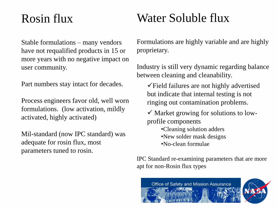
Rosin flux
Stable formulations – many vendors
have not requalified products in 15 or
more years with no negative impact on
user community.
Part numbers stay intact for decades.
Process engineers favor old, well worn
formulations. (low activation, mildly
activated, highly activated)
Mil-standard (now IPC standard) was
adequate for rosin flux, most
parameters tuned to rosin.
Water Soluble flux
Formulations are highly variable and are highly
proprietary.
Industry is still very dynamic regarding balance
between cleaning and cleanability.
Field failures are not highly advertised
but indicate that internal testing is not
ringing out contamination problems.
Market growing for solutions to low-
profile components•Cleaning solution adders
•New solder mask designs
•No-clean formulae
IPC Standard re-examining parameters that are more
apt for non-Rosin flux types

• 2008: 1 project using at GSFC
2010: 5 projects using at GSFC, JSC seeing usage, JPL
looking at internal process development.
• Flux qualification testing fell away after mil-spec retired
(~ 15 years ago). Old data being used to claim new IPC
type.
• Formulae include halogens which are not detected by
halide tests but which break down into halides during
activation. IPC types don’t tell the whole story.
• IPC and SMTA have heightened interest in flux and
cleaning concerns. Second biennial cleaning conference to
be held in November in Chicago. Rise in unpublished failures?

Electrostatic Discharge
Charge Device Model

(3) Parts and assemblies may be
exposed to more than one type
of ESD event over the
manufacturing and test life
cycle.
ESD Overview
(1) ESD Models Provide a way to characterize the
sensitivity of components to ESD
(2) The different ESD models simulate the different
environments experienced by electronic components
during the manufacturing process.
Courtesy ESP Seattle Inc.

HBMmature
MMmature
CDMevolving
HBM = Human Body Model
MM = Machine Model
CDM = Charged Device Model
Voltage discharged through
RC or RCL network creates
different total energy
experienced by the device.

White Paper 2: A Case for Lowering Component Level CDM ESD Specifications and
Requirements, Industry Council on ESD Target Levels, March 2009

2000X100XCourtesy of JPL Scott M. Hull NASA/GSFC
4600x
8600x
Courtesy of JPLCourtesy of JPL

HBM safety methods have brought HBM & MM
failures down to ~10% of failures encountered
industry-wide.
Role of CDM in failure count is now majority (~90%)
Examples of Sources of Threats (charge or
discharge path)
HBM MM CDM
Operator √
Work bench √
Pick and Place Machine √
Automatic Test Equipment √ √
Device package charging/discharging √
Mate/De-mate of harnesses √
RF Signals (including cell phone signals) √

CDM Challenges
- Opportunities to use on-chip ESD protection reduced in high
speed designs
- Reduction in conductor widths on-chip result in higher current
densities and thermal stress
- Package capacitances in high pin-count designs increase peak
current during CDM ESD event.
- Ionizers work on an HBM time scale and are not effective for
mitigating rapid-pulse charging events
Suppliers have been working to a 500V qualification level for
CDM (peak current @ 16A).
Industry position developing to reduce qualification level to 250V
(peak current @ 7A). increasing baseline risk

CDM Challenges
The area needed for
on-chip ESD
protection against
CDM events @ 16A
has become
impractical.
Gate damage susceptibility is scaling with
feature size.
Both are 45 nm technology, LV is Vdd=1.1V, MV is Vdd=1.8V
Typ
ica
l
Source: White Paper 2: A Case for Lowering Component Level CDM ESD Specifications and
Requirements, Industry Council on ESD Target Levels, March 2009

CDM Challenges
Capacitance must be reduced for high speed operation.
The remaining budget for ESDS circuitry scales downward
providing lower levels of ESD protection.
HSS = high speed signal
RC = resistor/capacitor
DTSCR = diode triggered
silicon controlled
rectifier
Source: White Paper 2: A Case for Lowering
Component Level CDM ESD Specifications and
Requirements, Industry Council on ESD Target Levels,
March 2009

CDM Challenges
Package size causes an increase in CDM event current. Package capacitance
charges triboelectrically or inductively and then discharges rapidly into the die
during the CDM event.

CDM - Summary• Devices will be less robust to CDM event in the future and “old”
practices may not be sufficient.
• Expert help will be needed to work through CDM safety
solutions. Complex and evolving event model.
• CDM safety measures may include new board materials, design
rules, discharge steps during test, protection from stray RF
• Technology drivers in high-speed, high pin-count devices make
them more susceptible to CDM events.
Suppliers will not “ESD harden” these devices
HBM methods will not protect these devices

High Density Interconnect
Printed Circuit Boards

• In 2008 a GSFC project encountered a printed wiring
assembly with a PCB that was failing batch-based quality
inspections.
• Extensive engineering and quality attention to this board
found that:
• HDI features such as buried vias, micro-vias, and a high layer count made it
very complex to manufacturer
• The system supplier did not have a PCB supplier who could identify and
control the critical processing parameters
Source: NASA GSFC
Courtesy: Coretec

• In December 2009 the IPC hosted a government-industry
symposium on the concerns of the US PCB industry.
• A major concern is a loss of the ability of US firms to
leverage off of high-volume commercial business to fund
capital equipment upgrades for their low-volume high-rel
customers (Mil and Space).
• Though device suppliers require state-of-the-art features,
PCB manufacturing capability is lagging and showing up as
quality defects.
Courtesy: Coretec

What is HDI?
Via Diameter ≤ .006” drilled; ≤ .003”
laser ablated
Pad-To-Hole Diameter
Difference
≤ .006”
Trace Width ≤ .003”
Spaces ≤ .003”
Pitch ≤ .010”
Through-Hole Aspect
Ratio (plating ratio)
12:1 +
Sequential Lamination 2 cycles +
Thin Dielectrics ≤ .003” reinforced;
≤ .001” unreinforced
Etch Features, Laser Drill, Embedded Passives,
Stacked/Staged Vias
0.003” = 0.072 mm
Source: HDI Implementation for
Aerospace/Military Applications, Gareth
Parry Chief Technology Officer, Coretec
Inc.

Interconnect Stress Testing (IST) should be investigated for
standard use by NASA in addition to coupon analysis.
Resistive heating and sense circuits built into PCB coupons can be
used to rapidly perform thermal cycling QCI testing.
Developer has demonstrated good correlation between field failures
and IST test failures.
Courtesy: PWB Interconnect Solutions Inc.

Summary (1 of 2)
(1) Disruptive technologies: timely access, low-cost, new performance
neglects some traditional features
new performance suite establishes price point
neglected features no longer affordable
(2) Disruptive technologies: characterization/reliability challenge
Not always a parts/materials quality challenge
More likely to be a design challenge
More GIDEPs at the System level?
(3) pH-neutral flux: Provides increased activity level and Green cleaning
Cleanliness requirements now more meaningful, not
well developed.
Reliability of voided joints (other than BGA) not
addressed.

Summary (2 of 2)
(4) CDM ESD Re-rating: Sacrifices ESD tolerance for high-speed performance
Clarifies performance capability to users though risk
mitigations may not be available.
CDM control methods are not standardized
CDM events expected to continue to dominate ESD
failures
(5) High Density Interconnect: HDI features enable high-speed performance
High equipment costs to support
Use of old equipment results in lack of lot control
(Quality problem)
Industry creating requirements
IST testing is an emerging option
PCB technology has become a significant assurance
concern for NASA (1st time?)
Top Related