


Languages
Pages
Legal


Faculty of Electrical Engineering and Information Technology
Ruhr-University Bochum, Germany
Diploma Thesis
Atomistic Modeling of an experimental
GaAs/InGaAs Quantum Dot Molecule using
NEMO 3-D
Yui-Hong “Matthias” Tan
In Partial Fulfillment of the Requirements for the Degree
Diplom-Ingenieur (Dipl.-Ing.)
Advisors
Prof. Dr. Gerhard Klimeck, Purdue University
Prof. Dr. Ulrich Kunze, Ruhr-University Bochum
September 2010
Purdue University
West Lafayette, Indiana, USA

i
I hereby affirm that I composed this work myself and did not use any but the denoted
resources.
West Lafayette, September 2010

ii
This thesis is dedicated to my parents
iii
ACKNOWLEDGEMENTS
First and foremost, I would like to thank my advisor Professor Dr. Gerhard Klimeck,
who has supported me throughout my graduate studies at Purdue University. I feel very
grateful for the opportunity to work in his research group and thankful for the excellent
resources. It would not have been possible for me to write this thesis without his guidance,
knowledge and patience. I would also like to express my gratitude to Professor Dr. Ulrich
Kunze at Ruhr-University Bochum. He has been a great mentor to me since the beginning
of my studies in Germany. I owe much of my accomplishments to his support, efforts and
encouragement. I am thankful to Dr. Muhammad Usman with whom I worked with for the
past two years. He was a valuable mentor and always a good friend, who taught me not
only about quantum dots, but also a lot about life as a graduate student. I feel fortunate to
have worked with him and wish him all the best in the future. Furthermore, I would like to
thank Dr. Peter Hommelhoff at the Max-Planck-Institute of Quantum Optics. He helped me
further understand the importance of always looking beyond your own field of expertise.
My experimental work on lasers in his group was a rewarding experience, which I value
very highly.
At this point, I would like to thank the German Academic Exchange Service for
funding and supporting my graduate studies. I would also like to express my sincere
gratitude to the German National Merit Foundation. I am deeply grateful for their support,
guidance and generosity, which often times went far beyond the academic realm. Being a
fellow of such a prestigious foundation has always been a privilege and great honor to me.

iv
TABLE OF CONTENTS
LIST OF TABLES…………………………………………………………………………v
LIST OF FIGURES…………………………………………………………………………vi
ABSTRACT………………………………………………………………………...…….....1
1. NEMO 3-D………………………………………………………………………………..2
2. INTRODUCTION TO QUANTUMDOTS……………………………………………...7
3. QUANTUM CONFINED STARK EFFECT……………………………………………..9
3.1 QCSE in single quantum dots……………………………………………………........9
3.2 QCSE in vertically stacked quantum dots…………………………………………...12
4. ATOMISTIC MODELING OF AN EXPERIMENTAL GaAs/InGaAs
QUANTUM DOT MOLECULE USING NEMO 3-D…………………………………..19
4.1. Abstract……………………………………………………………………………...19
4.2 Introduction…………………………………………………………………………..20
4.2.1 Motivation and Background of Problem…………………………………………20
4.2.2 Past Studies of Piezoelectric Effects……………………………………………..22
4.2.3 NEMO 3-D Simulator……………………………………………………………23
4.2.4 Simulated Geometry……………………………………………………………..24
4.3 Results………………………………………………………………………………..26
4.3.1 Experimental Emission from Excited States……………………………………….26
4.3.2 Observations of Anti-Crossings within the experimental field range……………...27
4.3.3 Electronic Spectrum Spectroscopy………………………………………………...29
5. IMPACT OF PIEZOELECTRICITY……………………………………………………36
5.1 Energy Spectrum Without and With Piezoelectricity……………………..................36
5.2 Piezoelectric Model.……………...………………………………………………….40
5.3 Quadrupole Nature of the Piezoelectric Potentials…………………………………..41
5.4 Quantitative Explanation of ‘One’ vs. ‘Two’ Anti-Crossings………………………..44
6. CONCLUSION………………………………………………………………………….47
LIST OF REFERENCES…………………………………………………………………..49

v
LIST OF TABLES
Table Page
Table 1: Polarization constants for calculation of piezoelectric potential……………….…42

vi
LIST OF FIGURES
Table Page
Figure 1.1: Sample single quantum dot structure as implemented in NEMO 3-D………….5
Figure 2.1 Single InAs quantum dot, quantitative band diagram…………………………...7
Figure 2.2 Stranski-Krastanov growth method……………………………………………...8
Figure 3.1 Single GaInAs quantum dot embedded in GaAs substrate………………………9
Figure 3.2 First three electron states and uppermost hole state of the single quantum dot..10
Figure 3.3 Exciton E1-H1, single quantum dot structure…………………………………..11
Figure 3.4 Effect of electric fields in single quantum dots………………………………...11
Figure 3.5 a) Hole level H1 and b) electron level E1 of single quantum dot structure…….12
Figure 3.6 Quantitative depiction of direct and indirect exciton…………………………..13
Figure 3.7 Two vertically stacked GaInAs quantum dots embedded in GaAs…………….14
Figure 3.8 Exciton spectrum of vertically stacked quantum dot structure…………………14
Figure 3.9 Wavefunction plots of the first three electron states and uppermost hole state...15
Figure 3.10 single electron and hole state energies of vertically stacked quantum dots…...16
Figure 3.11 Two vertically stacked GaInAs quantum dots with d = 5nm………………….16
Figure 3.12 Band diagram of vertically stacked quantum dot structure for different d……17
Figure 3.13 Comparison of Stark shift for different interdot separation distances………...18
Figure 4.1 Schematic of quantum dot molecule, plot of excitonic spectrum………………25
Figure.4.2 Qualitative band diagram plot of quantum dot molecule………………………28
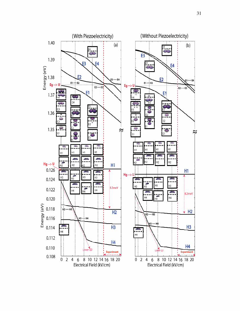
Figure 4.3 Spectroscopy of quantum dot molecule………………………………………...31
Figure 5.1 Piezoelectric potential profiles…………………………………………………43
Figure 5.2 Comparison of results with and without piezoelectric effects included………..46

1
ABSTRACT
Over the last decade, the ongoing improvement of nanofabrication technologies has opened
the way for novel nano-devices and semiconductor structures with sizes of a few tens of
nanometers. One realization of such semiconductor devices can be found in the application
of quantum dots. Quantum dots are characterized by their ability to confine carriers in all
three spatial dimensions on a nanometer scale.
Quantum dots are often referred to as “artificial atoms” with discrete atomic-like energy
states resulting from quantum mechanical carrier confinement. Quantum dot structures
therefore offer us the opportunity to study quantum mechanical effects of atomic systems
on a nanometer scale. From an application point of view quantum dots find use in a wide
spectrum of areas ranging from lasers, photo detectors and lighting to medical imaging.
Quantum dot structures are also intensely studied as promising candidates in the realization
of quantum computing applications.
The main work of this thesis comprises a theoretical study of an experimentally
investigated InGaAs quantum dot molecule. Using NEMO-3D to perform atomistic
electronic structure calculations on a multi-million atom scale, we quantitatively reproduce
and analyze an experimentally measured excitonic spectrum of the examined InGaAs
quantum dot molecule. Furthermore, we highlight and discuss the importance of
piezoelectric effects in achieving agreement of our simulations results with the
experimental excitonic spectrum.
In the first chapters, we present a short introduction to quantum dots and the Quantum
Confined Stark Effect, illustrated by simulations of single and vertically stacked quantum
dot structures. The subsequent chapters will continue with the study on the InGaAs
quantum dot molecule and focus our discussion on the experimental excitonic spectrum.

2
1. NEMO-3D
The simulations of the quantum dot structures in this thesis were carried out using the 3-D
NanoElectronic Modeling (NEMO-3D) tool. The software enables the atomistic simulation
and computation of strain and electronic structure in multi-million atoms nanostructures.
NEMO 3-D can handle strain and electronic structure calculations consisting of more than
64 and 52 million atoms, corresponding to nanostructures of (110nm) 3
and (101nm) 3
,
respectively. [50]
Applications of NEMO 3-D in realistically sized nanostructures include self-assembled
single quantum dots, stacked quantum dot systems, SiGe quantum wells, SiGe nanowires
and nanocrystals. [14]
NEMO-3D is the successor of the 1D Nanoelectronic modeling tool (NEMO) and was
developed by Professor Dr. Gerhard Klimeck on Linux clusters at the NASA Jet Propulsion
Laboratory. NEMO 3-D was released in 2003 and is until now used in simulation tools on
nanoHUB.org reaching out to and impacting the work of thousands of users. NEMO 3-D
runs on serial and parallel platforms, local cluster computers, as well as the National
Science Foundation Teragrid. For a detailed view on the development of NEMO-3D the
reader may be referred to the following publications. [13, 14, 15]
In the following, I would like to outline the underlying physical models and concepts used
in NEMO 3-D and subsequently continue with a sample case study of a single quantum dot
to illustrate the general simulation flow of NEMO 3-D.
As modern nanoelectronic structures reach size domains of few tens of nanometers, the
quantum mechanical nature of charge carriers becomes an important factor in modeling and
determining nanoelectronic device properties. The atomic granularity of materials in these
small regimes cannot be neglected and has to be considered to accurately model latest
nanoelectronic devices.

3
To address the issues of pronounced quantum mechanical effects and atomic granularity,
atomistic approaches therefore seem favorable in simulating electronic band structures in
realistically sized nanoelectronic devices. Atomistic models aim to incorporate the
electronic wave function of each individual atom.
The electronic band structure calculation in NEMO 3-D is based on a twenty band
sp3d
5s* nearest neighbor tight-binding model, which includes spin. Choosing the tight-
binding model allows electronic structure simulation in atomistic resolution and is suitable
to model finite device sizes, alloy disorder or heterointerfaces.
In the tight-binding formalism a basis is defined from a selection of atomic orbitals (e.g.
s, p, and d) centered on each atom of the crystal, which create a single electron Hamiltonian.
The Hamiltonian represents the electronic properties of the bulk material. Interactions
between nearest neighbor atoms and between different orbitals within an atom are included
by using empirical fitting parameters. Fitting parameters entering the electronic band
structure calculation must be obtained or adjusted for each constituent material and bond
type and verified against experimental data.
The need for empirical fitting parameters results in the major drawback of the tight-
binding model and still continues to raise questions within the community about the
fundamental applicability of tight-binding. Although tight binding requires empirical fitting,
its advantages over comparable methods made tight binding the appropriate choice in the
development of NEMO 3-D. For example, non-atomistic continuum methods such as
effective mass or k*p typically fail to capture the atomic granularity of materials inherent in
the tight binding model.
Non-atomistic approaches do not model each atom individually in the structure, but
rather approximate the underlying structure based on a continuous, jelly-type view of
matter. This simplified description of matter makes non-atomistic models not well suited to
address interface or disorder effects in nano-scale regimes.
4
Alternative atomistic approaches like pseudopotentials use plane waves as a fundamental
basis choice. But with realistic nanostructures containing high-frequency features arising
from alloy disorder or heterointerfaces, the basis needs to be adjusted each time for every
different device. Besides the complex adjustment procedure, the numerical implementation
of pseudopotential calculations is computationally more challenging as compared to tight
binding.
To address the issue of empirical fitting in tight binding and take advantage of the
model’s full potential, the NEMO team spent significant effort to successfully expand and
document the tight-binding capabilities. [40,42,43,44,45] Using tight binding, NEMO was
able, for example, to early match experimentally obtained current-voltage curves of
resonant tunneling diodes that could not be modeled by either effective mass or
pseudopotential methods [13].
Strain plays an important role in nano-devices and its effects have to be taken into
account to achieve accurate and realistic modeling in the nano-scale regime. In quantum
dot structures, strain arises due to the lattice mismatch between the quantum dot and
substrate material. For example, the difference in lattice constants in a typical InAs/GaAs
system is on the order of 7% [13]. The effects of strain will be dealt with in more detail in
the following chapters.
NEMO 3-D is capable of computing strain fields using an atomistic valence force field
(VFF) method with the Keating potential [13]. In this model, the total elastic energy of the
structure is obtained as a sum of bond-stretching and bond-bending contributions from each
atom. The total elastic energy is then minimized to find the equilibrium atomic positions of
each atom. To illustrate the program flow of NEMO 3-D, a typical simulation of a single
quantum dot is presented. The general geometry of the structure is depicted in Figure 1. [14]

5
Figure 1.1: Sample single quantum dot structure as implemented in NEMO 3-D, [14]
The structure consists of a single dome-shaped InAs quantum dot, which is embedded in a
GaAs substrate. The dot has a diameter of 11.3nm and height of 5.65nm and is placed on a
wetting layer of 0.6nm thickness. The electronic structure calculation is carried out in the
small box Delec , which contains around 0.3 million atoms. The strain domain Dstrain, which
contains around 3 million atoms, is chosen to be larger to sufficiently capture long-ranging
strain fields. The calculation in the electronic box assumes closed boundary conditions
whereas the strain domain assumes open boundary conditions in the lateral dimensions and
open boundary conditions on the top surface.
The NEMO 3-D simulation flow consists of four main components. [13] In the first part
of the simulation, the geometry is constructed in atomistic detail. In this process, each atom
is assigned a three single-precision number to identify its position within the structure.
Furthermore, the geometry constructor saves the atomic number of each atom, the
information whether the atom lies on the surface or not, the nearest neighbor relation of the
atom in a unit cell and the information whether the atom is included only in the strain
calculation or in both the strain and electronic calculation. In the second part, NEMO 3-D
by default calculates the strain in the system based on an atomistic valence force field (VFF)
approach. If desired, the strain calculation can be deactivated. This option is useful, if one
wants to investigate structures without including possible strain effects, for example.

6
Subsequent to the calculation of the strain profile, NEMO 3-D starts computing the
single-particle energies and wave functions using a 20 band atomistic nearest neighbor
tight-binding model. The computation of the electronic structure is algorithmically and
computationally more challenging than the strain calculation and involves handling of
matrices on the order of millions. Available algorithms and solvers for the electronic
structure calculation in NEMO 3-D include the PARPACK library and a custom
implementation of the Lanczos method.[13] From the single-particle eigenstates, NEMO 3-
D allows post processing calculations of various physical properties such as optical matrix
elements or piezoelectric potentials and the graphical display of wavefunctions using
Rappture.[13]
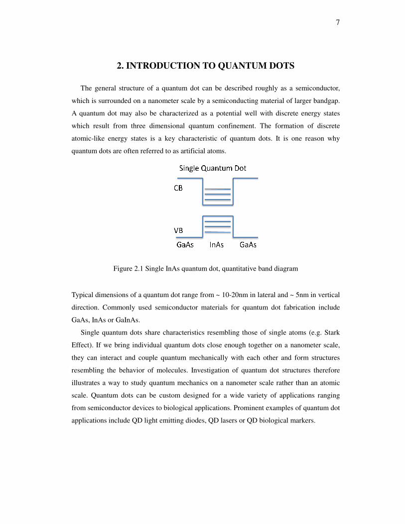
2. INTRODUCTION TO QUANTUM
The general structure of a quantum dot can be described roughly as a semiconductor
which is surrounded on a nanometer scale by a semiconducting material of larger bandgap.
A quantum dot may also be characterized as a potential well with discr
which result from three dimensional quantum confinement. The formation of discrete
atomic-like energy states is a key characteristic of quantum dots. It is one reason why
quantum dots are often referred to as artificial atoms.
Figure 2.1 Single InAs quantum dot, quantitative band diagram
Typical dimensions of a quantum dot range from ~ 10
direction. Commonly used semiconductor materials for quantum dot fabrication include
GaAs, InAs or GaInAs.
Single quantum dots share characteristics resembling those of single atoms (e.g. Stark
Effect). If we bring individual quantum dots close enough together on a nanometer scale,
they can interact and couple quantum mechanically with each other and form
resembling the behavior of molecules. Investigation of quantum dot structures therefore
illustrates a way to study quantum mechanics on a nanometer scale rather than an atomic
scale. Quantum dots can be custom designed for a wide variety of appl
from semiconductor devices to biological applications. Prominent examples of quantum dot
applications include QD light emitting diodes, QD lasers or QD biological markers.
INTRODUCTION TO QUANTUM DOTS
The general structure of a quantum dot can be described roughly as a semiconductor
which is surrounded on a nanometer scale by a semiconducting material of larger bandgap.
A quantum dot may also be characterized as a potential well with discrete energy states
which result from three dimensional quantum confinement. The formation of discrete
like energy states is a key characteristic of quantum dots. It is one reason why
quantum dots are often referred to as artificial atoms.
1 Single InAs quantum dot, quantitative band diagram
Typical dimensions of a quantum dot range from ~ 10-20nm in lateral and ~ 5nm in vertical
direction. Commonly used semiconductor materials for quantum dot fabrication include
Single quantum dots share characteristics resembling those of single atoms (e.g. Stark
Effect). If we bring individual quantum dots close enough together on a nanometer scale,
they can interact and couple quantum mechanically with each other and form structures
resembling the behavior of molecules. Investigation of quantum dot structures therefore
illustrates a way to study quantum mechanics on a nanometer scale rather than an atomic
Quantum dots can be custom designed for a wide variety of applications ranging
from semiconductor devices to biological applications. Prominent examples of quantum dot
applications include QD light emitting diodes, QD lasers or QD biological markers.
7
The general structure of a quantum dot can be described roughly as a semiconductor,
which is surrounded on a nanometer scale by a semiconducting material of larger bandgap.
ete energy states
which result from three dimensional quantum confinement. The formation of discrete
like energy states is a key characteristic of quantum dots. It is one reason why
20nm in lateral and ~ 5nm in vertical
direction. Commonly used semiconductor materials for quantum dot fabrication include
Single quantum dots share characteristics resembling those of single atoms (e.g. Stark
Effect). If we bring individual quantum dots close enough together on a nanometer scale,
structures
resembling the behavior of molecules. Investigation of quantum dot structures therefore
illustrates a way to study quantum mechanics on a nanometer scale rather than an atomic
ications ranging
from semiconductor devices to biological applications. Prominent examples of quantum dot
8
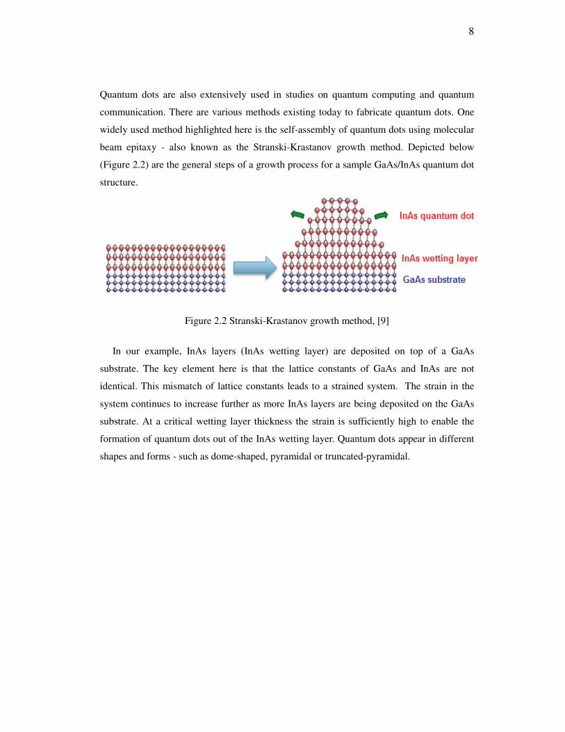
Quantum dots are also extensively used in studies on quantum computing and quantum
communication. There are various methods existing today to fabricate quantum dots. One
widely used method highlighted here is the self-assembly of quantum dots using molecular
beam epitaxy - also known as the Stranski-Krastanov growth method. Depicted below
(Figure 2.2) are the general steps of a growth process for a sample GaAs/InAs quantum dot
structure.
Figure 2.2 Stranski-Krastanov growth method, [9]
In our example, InAs layers (InAs wetting layer) are deposited on top of a GaAs
substrate. The key element here is that the lattice constants of GaAs and InAs are not
identical. This mismatch of lattice constants leads to a strained system. The strain in the
system continues to increase further as more InAs layers are being deposited on the GaAs
substrate. At a critical wetting layer thickness the strain is sufficiently high to enable the
formation of quantum dots out of the InAs wetting layer. Quantum dots appear in different
shapes and forms - such as dome-shaped, pyramidal or truncated-pyramidal.
3. QUANTUM CONFINED STARK EFFECT
3.1 QCSE in single quantum dots
In chemistry, the Stark effect describes the shifting and splitting of spectral lines
atoms and molecules in the presence of an applied external electric field.
Stark effect is the Quantum Confined Stark Effect, which describes the effect of external
electric fields on the absorption spectrum in semiconductor quantum wells and quantum
dots. Tunability of the absorption spectrum based on the QCSE is an effi
making optical modulators and self
The work in this Studienarbeit focuses on the theoretical study of the QCSE in single
quantum dots and vertically stacked quantum dot pairs. All the simulations were
using 3-D NanoElectronic Modeling
the Quantum Confined Stark Effect in a GaInAs single quantum dot.
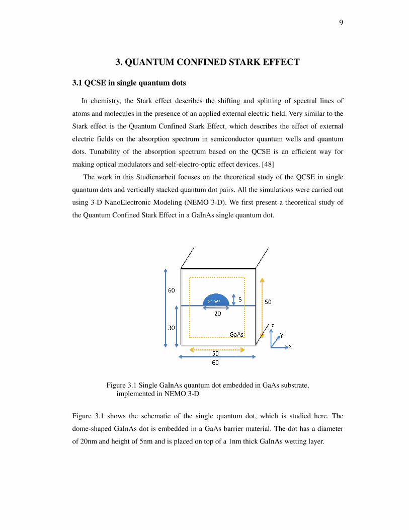
Figure 3.1 Single GaInAs quantum dot embedded in GaAs substrate,
implemented in NEMO 3
Figure 3.1 shows the schematic of the single quantum dot, which is studied here.
dome-shaped GaInAs dot is embedded in a GaAs barrier material. The dot has a diameter
of 20nm and height of 5nm and is pla
3. QUANTUM CONFINED STARK EFFECT
3.1 QCSE in single quantum dots
In chemistry, the Stark effect describes the shifting and splitting of spectral lines
atoms and molecules in the presence of an applied external electric field. Very similar
Stark effect is the Quantum Confined Stark Effect, which describes the effect of external
electric fields on the absorption spectrum in semiconductor quantum wells and quantum
dots. Tunability of the absorption spectrum based on the QCSE is an efficient way for
making optical modulators and self-electro-optic effect devices. [48]
The work in this Studienarbeit focuses on the theoretical study of the QCSE in single
quantum dots and vertically stacked quantum dot pairs. All the simulations were carried out
D NanoElectronic Modeling (NEMO 3-D). We first present a theoretical study of
the Quantum Confined Stark Effect in a GaInAs single quantum dot.
Single GaInAs quantum dot embedded in GaAs substrate,
implemented in NEMO 3-D
shows the schematic of the single quantum dot, which is studied here.
shaped GaInAs dot is embedded in a GaAs barrier material. The dot has a diameter
of 20nm and height of 5nm and is placed on top of a 1nm thick GaInAs wetting layer.
9
In chemistry, the Stark effect describes the shifting and splitting of spectral lines of
Very similar to the
Stark effect is the Quantum Confined Stark Effect, which describes the effect of external
electric fields on the absorption spectrum in semiconductor quantum wells and quantum
cient way for
The work in this Studienarbeit focuses on the theoretical study of the QCSE in single
carried out
. We first present a theoretical study of
shows the schematic of the single quantum dot, which is studied here. The
shaped GaInAs dot is embedded in a GaAs barrier material. The dot has a diameter
ced on top of a 1nm thick GaInAs wetting layer.

10
To capture the effects of long-range strain fields penetrating into the barrier material, the
strain domain is chosen sufficiently large. The strain domain comprises a box with side
lengths of 60, 60 and 68nm. The electronic structure calculation is done within the box
outlined by the yellow dashed lines. The electronic domain has a size of 50x50x50nm.
Figure 3.2 shows a graphical representation of the first three electron states (E1,E2,E3) and
the uppermost hole state H1 for no electric field applied and viewed from the top of the
structure (-z direction).
Figure 3.2 First three electron states and uppermost hole state of the single quantum dot
structure described in Figure 3.1, obtained from NEMO 3-D and Rappture
To investigate the Quantum Confined Stark Effect under varying electric field strengths,
we apply an electric field in positive z-direction and sweep the electric field strength from -
15kV/cm to 15kV/cm. A complete simulation run for one electric field value carried out on
the Coates cluster machines with 56 processors took approximately 5-6 hours. Figure 3.3
shows the energy of exciton (E1-H1) plotted against the electric field. In correspondence
with published literature on single quantum dots, our results obtained from NEMO 3-D
show a parabolic Stark shift. [49]

Figure 3.3 Exciton E1
results obtained from NEMO 3
For further investigation on the parabolic Stark shift behavior,
qualitative sketch of the band diagram.
dimensions, discrete levels form within the quantum dot. Depicted in the figure are
lowest electron level E1 and the uppermost valence band hole state H1. If an electric field
is applied along the growth direction of the quantum dot as shown in the figure, the energy
difference Eg between E1 and H1 reduces.
Figure 3.4 Effect of elect
Exciton E1-H1, single quantum dot structure, see Figure 3.1.
results obtained from NEMO 3-D
For further investigation on the parabolic Stark shift behavior, figure 3.4 shows a
qualitative sketch of the band diagram. Due to carrier confinement in all three spatial
dimensions, discrete levels form within the quantum dot. Depicted in the figure are
lowest electron level E1 and the uppermost valence band hole state H1. If an electric field
is applied along the growth direction of the quantum dot as shown in the figure, the energy
between E1 and H1 reduces.
Effect of electric fields in single quantum dots
11
shows a
Due to carrier confinement in all three spatial
dimensions, discrete levels form within the quantum dot. Depicted in the figure are the
lowest electron level E1 and the uppermost valence band hole state H1. If an electric field
is applied along the growth direction of the quantum dot as shown in the figure, the energy

12
Due to the tilted potential profile in the case of an applied bias, E1 shifts towards the
lower left corner of the well and thus decreases in energy. H1 on the other hand, moves up
in energy towards the upper right corner of the well. The net effect is thus a lowering of the
energy band gap energy (E1-H1). Figures 3.5a and b show the simulated results of the
single states E1 and H1 as a function of electric field. The vertex of the parabola of H1 is
not centered on zero electric field. This behavior can be attributed to strain effects and the
general asymmetry of the dome-shaped quantum dot.
Figure 3.5 a) Hole level H1 and b) electron level E1 of single quantum dot structure
(Fig. 3.1) plotted against electric field
3.2 QCSE in vertically stacked quantum dots
In the following, we present a theoretical study on the Quantum Confined Stark Effect in
vertically stacked quantum dot structures. The Quantum Confined Stark Effect in vertically
stacked quantum dots can exhibit parabolic as well linear dependence on the electric field.
Whether we observe linear or parabolic dependence is largely determined by the location of
the hole and electron state forming the exciton under investigation.

Figure 3.6 Quantitative depiction of direct and indirect exciton. If both hole and electron
are in the same dot (direct), if electron and hole are in different dots (indirect)
Figure 3.6 illustrates the direct and indirect exciton in the band
Characterized by the slope of the potential, the electric field in both the upper and lower
band diagram is of equal magnitude. In figure
lower quantum dot and thus form a direct excito
located in the upper dot, whereas E1 is still in the lower dot. Since the energy band gap E
in figure 3.6 b) is smaller than E
the indirect exciton. The structure considered in our study on vertically stacked quantum
dots is depicted in figure 3.7 and shows two vertically stacked dome
quantum dots. Both dots have identical diameter and height sizes of 20 and 5 nm,
respectively. The dots are surrounded by a GaAs substrate of side lengths 60, 60 and 68nm
and placed on top of 1nm thick GaInAs wetting layers. The dimensions of the electronic
calculation domain (50x50x36nm) are marked by the yellow dashed lines. The distance
between the quantum dots as measured from the wetting layers is 12 nm. Just as in the
single quantum dot structure, the electric field is applied in positive z
from -20 kV/cm to 20 kV/cm.
Figure 3.6 Quantitative depiction of direct and indirect exciton. If both hole and electron
are in the same dot (direct), if electron and hole are in different dots (indirect)
illustrates the direct and indirect exciton in the band diagram representation.
Characterized by the slope of the potential, the electric field in both the upper and lower
band diagram is of equal magnitude. In figure 3.6 a) the electron and hole state are in the
lower quantum dot and thus form a direct exciton. In figure 3.6 b), the hole state H1 is
located in the upper dot, whereas E1 is still in the lower dot. Since the energy band gap E
is smaller than Eg in figure 3.6 a), a larger Stark shift will be observed for
The structure considered in our study on vertically stacked quantum
dots is depicted in figure 3.7 and shows two vertically stacked dome-shaped GaInAs
quantum dots. Both dots have identical diameter and height sizes of 20 and 5 nm,
re surrounded by a GaAs substrate of side lengths 60, 60 and 68nm
and placed on top of 1nm thick GaInAs wetting layers. The dimensions of the electronic
calculation domain (50x50x36nm) are marked by the yellow dashed lines. The distance
dots as measured from the wetting layers is 12 nm. Just as in the
single quantum dot structure, the electric field is applied in positive z-direction and varied
13
Figure 3.6 Quantitative depiction of direct and indirect exciton. If both hole and electron
diagram representation.
Characterized by the slope of the potential, the electric field in both the upper and lower
the electron and hole state are in the
, the hole state H1 is
located in the upper dot, whereas E1 is still in the lower dot. Since the energy band gap Eg
a larger Stark shift will be observed for
The structure considered in our study on vertically stacked quantum
shaped GaInAs
quantum dots. Both dots have identical diameter and height sizes of 20 and 5 nm,
re surrounded by a GaAs substrate of side lengths 60, 60 and 68nm
and placed on top of 1nm thick GaInAs wetting layers. The dimensions of the electronic
calculation domain (50x50x36nm) are marked by the yellow dashed lines. The distance
dots as measured from the wetting layers is 12 nm. Just as in the
direction and varied
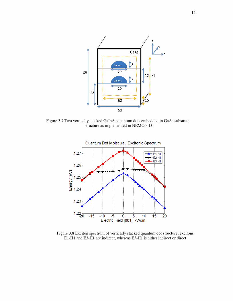
Figure 3.7 Two vertically stacked GaInAs quantum dots
structure as implemented in NEMO 3
Figure 3.8 Exciton spectrum of vertically stacked quantum dot structure, excitons
E1-H1 and E3-H1 are indirect, whereas E3
Two vertically stacked GaInAs quantum dots embedded in GaAs substrate,
structure as implemented in NEMO 3-D
Exciton spectrum of vertically stacked quantum dot structure, excitons
H1 are indirect, whereas E3-H1 is either indirect or direct
14
embedded in GaAs substrate,
Exciton spectrum of vertically stacked quantum dot structure, excitons
direct

15
Figure 3.8 shows the simulated excitonic spectrum of the quantum dot molecule obtained
from NEMO 3-D. Three excitons labeled E1-H1, E2-H1 and E3-H1 are displayed. Excitons
E1-H1 and E3-H1 are indirect, whereas exciton E2-H1 changes from direct to indirect at
different electric field strengths. To further elucidate the obtained exciton spectrum, figure
3.9 shows wave plots of the uppermost hole state and the first three electron states for
various electric field strengths. For example, at an electric field strength of 5kV/cm, exciton
E2-H1 is direct (E2 and H1 both in upper dot). This explains the smaller Stark shift
observed for exciton E2-H1. On the other hand, as we increase the bias beyond 10 kV/cm,
E2 will eventually move into the lower dot. Exciton E2-H1 then changes its type from
direct to indirect, which will also be reflected in a stronger Stark shift.
Figure 3.9 wave function plots of the first three electron states and uppermost hole state for
different electric field values, vertically stacked quantum dot structure (fig.3.1)
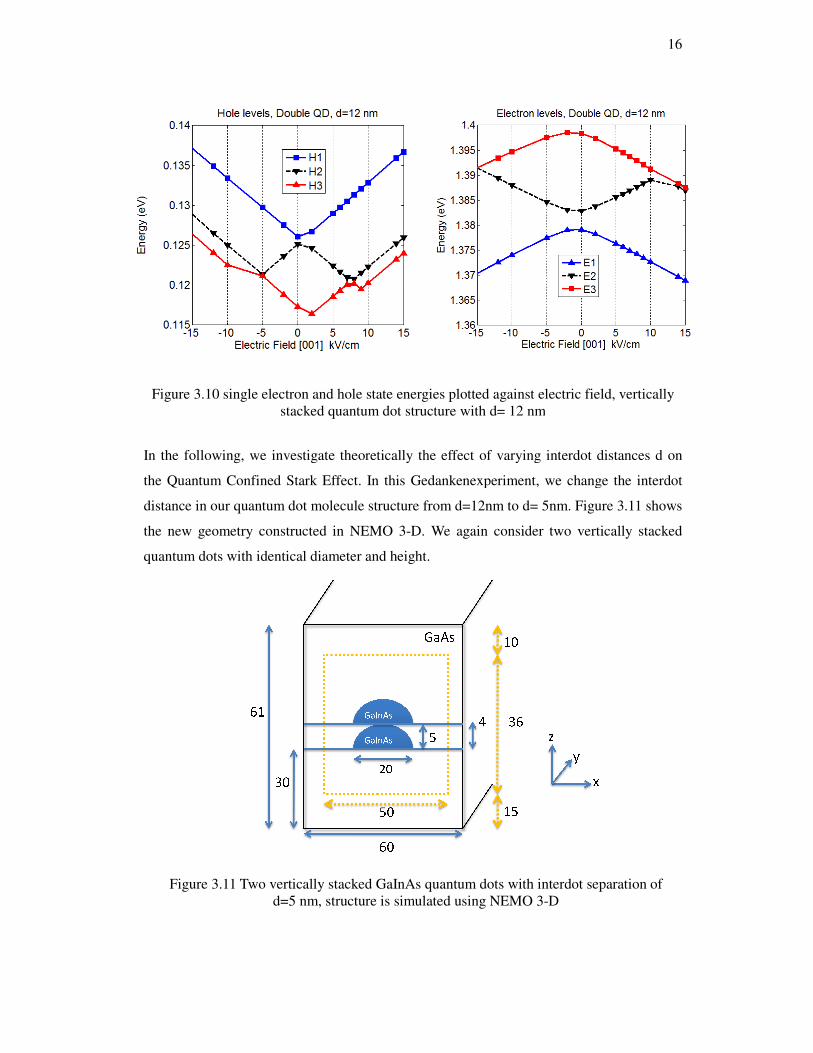
Figure 3.10 single electron and hole state energies plotted against electric field, vertically
stacked quantum dot structure with d= 12 nm
In the following, we investigate theoretically the effect of varying interdot distances d on
the Quantum Confined Stark Effect. In this Gedankenexperiment, we change the interdot
distance in our quantum dot molecule structure from d=12nm to d= 5nm. Figure 3.11 shows
the new geometry constructed in NEMO 3
quantum dots with identical diameter and height.
Figure 3.11 Two vertically stacked GaInAs quantum dots with interdot separation of
d=5 nm, structure is simulated using NEMO 3
single electron and hole state energies plotted against electric field, vertically
stacked quantum dot structure with d= 12 nm
investigate theoretically the effect of varying interdot distances d on
the Quantum Confined Stark Effect. In this Gedankenexperiment, we change the interdot
distance in our quantum dot molecule structure from d=12nm to d= 5nm. Figure 3.11 shows
ometry constructed in NEMO 3-D. We again consider two vertically stacked
quantum dots with identical diameter and height.
Two vertically stacked GaInAs quantum dots with interdot separation of
d=5 nm, structure is simulated using NEMO 3-D
16
single electron and hole state energies plotted against electric field, vertically
investigate theoretically the effect of varying interdot distances d on
the Quantum Confined Stark Effect. In this Gedankenexperiment, we change the interdot
distance in our quantum dot molecule structure from d=12nm to d= 5nm. Figure 3.11 shows
D. We again consider two vertically stacked
Two vertically stacked GaInAs quantum dots with interdot separation of

Figure 3.12 Band diagram of vertically stacked quantum dot structure for a) large dot
separation and b) small dot separation
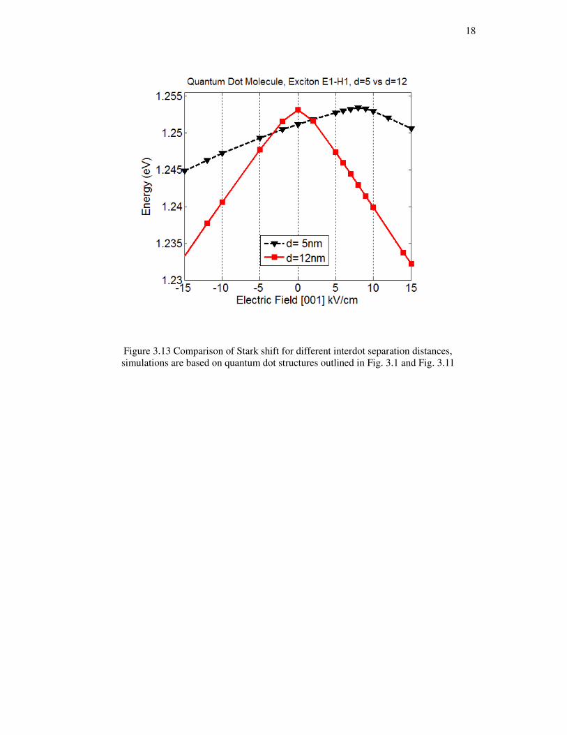
To qualitatively illustrate the effects of varying interdot separation distances, consider the
band diagrams depicted in figure 3.12 a, b). In both band diagrams, the same electric field
is applied. In figure 3.12 b) however, the distance d between the dots is reduced. This leads
to a shorter “lever arm” and thus a smaller Stark shift for the same electric field strength.
Therefore one can conclude that a smaller dot separation d results in less pronounced Stark
shifts. In our simulations using NEMO 3
varying interdot distances. Figure 3.13 shows a comparison of exciton E1
different interdot separations d= 5nm and d= 12nm based on the quantum dot structures in
figure 3.1 and figure 3.11. In accordance with theory, we observe a drastically reduced
Stark shift in the case of d= 5nm. Furthermore, we note that the ma
d=5 nm is not centered at zero electric field. This asymmetry can be attributed to stronger
strain fields in the case of smaller dot separations. As the quantum dots separation
decreases, the coupling due to strain and quantum mechani
more pronounced.
Band diagram of vertically stacked quantum dot structure for a) large dot
separation and b) small dot separation
To qualitatively illustrate the effects of varying interdot separation distances, consider the
figure 3.12 a, b). In both band diagrams, the same electric field
is applied. In figure 3.12 b) however, the distance d between the dots is reduced. This leads
to a shorter “lever arm” and thus a smaller Stark shift for the same electric field strength.
erefore one can conclude that a smaller dot separation d results in less pronounced Stark
shifts. In our simulations using NEMO 3-D, we could successfully verify these effects of
Figure 3.13 shows a comparison of exciton E1-H1 for the two
different interdot separations d= 5nm and d= 12nm based on the quantum dot structures in
figure 3.1 and figure 3.11. In accordance with theory, we observe a drastically reduced
Stark shift in the case of d= 5nm. Furthermore, we note that the maxima of the curve for
d=5 nm is not centered at zero electric field. This asymmetry can be attributed to stronger
strain fields in the case of smaller dot separations. As the quantum dots separation
decreases, the coupling due to strain and quantum mechanical interaction effects become
17
Band diagram of vertically stacked quantum dot structure for a) large dot
To qualitatively illustrate the effects of varying interdot separation distances, consider the
figure 3.12 a, b). In both band diagrams, the same electric field
is applied. In figure 3.12 b) however, the distance d between the dots is reduced. This leads
to a shorter “lever arm” and thus a smaller Stark shift for the same electric field strength.
erefore one can conclude that a smaller dot separation d results in less pronounced Stark
D, we could successfully verify these effects of
for the two
different interdot separations d= 5nm and d= 12nm based on the quantum dot structures in
figure 3.1 and figure 3.11. In accordance with theory, we observe a drastically reduced
xima of the curve for
d=5 nm is not centered at zero electric field. This asymmetry can be attributed to stronger
strain fields in the case of smaller dot separations. As the quantum dots separation
cal interaction effects become
18
Figure 3.13 Comparison of Stark shift for different interdot separation distances,
simulations are based on quantum dot structures outlined in Fig. 3.1 and Fig. 3.11
19
4. ATOMISTIC MODELING OF AN EXPERIMENTAL
GaAs/InGaAs QUANTUM DOT MOLECULE USING NEMO 3-D
4.1. Abstract
Atomistic electronic structure calculations are performed to study the coherent inter-dot
couplings of the electronic states in a single InGaAs quantum dot molecule. The
experimentally observed excitonic spectrum [12] is quantitatively reproduced, and the
correct energy states are identified based on a previously validated atomistic tight binding
model. The extended devices are represented explicitly in space with 15 million atom
structures. An excited state spectroscopy technique is presented in which the externally
applied electric field is swept to probe the ladder of the electronic energy levels (electron or
hole) of one quantum dot through anti-crossings with the energy levels of the other
quantum dot in a two quantum dot molecule. Such a technique can be applied to estimate
the spatial electron-hole spacing inside the quantum dot molecule as well as to reverse
engineer the quantum dot geometry parameters such as the quantum dot separation. Crystal
deformation induced piezoelectric effects have been discussed in the literature as minor
perturbations lifting degeneracies of the electron excited (P and D) states, thus affecting
polarization alignment of wave function lobes for III-V Heterostructures such as single
InAs/GaAs quantum dots. In contrast, this work demonstrates the crucial importance of
piezoelectricity to resolve the symmetries and energies of the excited states through
matching the experimentally measured spectrum in an InGaAs quantum dot molecule under
the influence of an electric field. Both linear and quadratic piezoelectric effects are studied
for the first time for a quantum dot molecule and demonstrated to be indeed important. The
net piezoelectric contribution is found to be critical in determining the correct energy
spectrum, which is in contrast to recent studies reporting vanishing net piezoelectric
contributions.

20
4.2. Introduction
4.2.1 Motivation and Background of Problem
Quantum dots grown by strain driven self-assembly attract much interest because they
can be used to implement optical communication and quantum information processing [1,
2]. Recently, significant advancements in providing good stability, high repetition rate,
electroluminescence, and controlled coupling have made III-V quantum dots a potential
candidate for quantum computers. Based on single qubit (quantum bit) realization with an
exciton in a single quantum dot [3], optical quantum gates also have been obtained with
both an exciton and a biexciton within one dot [4]. Coupled quantum dot molecules
(QDMs), therefore, are good candidates for spin-based [5], charge-based [6], and exciton-
based [7, 8] qubits. It is desirable to excite single excitons with external electric fields.
Vertically stacked QDMs have been suggested to host single or double qubits; these can
then be controlled by optical pulses, electrical fields, or magnetic fields [7-11]. However, a
very basic requirement necessary for realizing qubits in these structures is the prior
achievement of entangled states between the two dots.
In a recent experimental study [12], coherent quantum coupling in QDMs has been
observed with different separation distances between two dots forming a QDM under the
applied bias. However a detailed quantitative study for the identification of the states in the
spectrum and their coupling under linear and quadratic piezoelectric effects has been
missing. The theoretical study accompanied with the experiment [12] is based on a single
band effective mass model and considered only two lowest conduction band (E1 and E2)
energy levels and two highest valence band (H1 and H2) energy levels. Thus the figure 3(b)
in reference [12] plots only one anti-crossing (E1↔H1) and compares it to the experimental
measurement.
Moreover, it did not take into account the effects of the nonlinear piezoelectricity,
because the nonlinear piezoelectric field polarization constants [24] were not available at
the time of this study in 2005.

21
Thus the published study did not include the symmetries of individual quantum dots nor
did it model the energy state couplings quantitatively. In a quantum dot molecule, each
quantum dot possesses a ladder of electronic energy levels, which give rise to multiple anti-
crossings due to the electrical field induced Stark shift. It is therefore essential that more
than two electron and hole energy levels should be considered to identify the correct energy
states in the experimental measurements.
In this work, we present an atomistic theoretical analysis of the experimental
measurement including alloy randomness, interface roughness, atomistic strain and
piezoelectric induced polarization anisotropy, and realistic sized boundary conditions,
which we believe is essential to fully understand the complex physics of these multi-million
atom nanostructures [16]. Both linear and nonlinear components of the piezoelectric field
are included. The net piezoelectric field is found to be critical to resolve the symmetries and
energies of the excited states. Our theoretical optical transition strengths match with the
experimental quantum dot state coupling strengths.
Furthermore, we sweep the externally applied electrical field from zero to 21kV/cm to
probe the symmetry of the electron states in the lower quantum dot based on the inter-dot
energy level anti-crossings between the lower and the upper quantum dots. Such „level
anti-crossing spectroscopic‟ (LACS) analysis [37] can be used for a direct and precise
measurement of the energy levels of one quantum dot placed near another quantum dot in
the direction of the applied electrical field. It can also be helpful to quantitatively analyze
„tunnel coupling energies‟ of the electron and hole energy states through inter-dot energy
level resonances in the single quantum dot molecule configuration predicted for „quantum
information technologies‟ [12].
Finally the spacing between the anti-crossings and electrical field induced stark shifts
allow us to „reverse engineer‟ the separation between the quantum dots inside the quantum
dot molecule. Quantum dot molecules grown by self-assembly are mechanically coupled to
each other through long-range strain originating from lattice mismatch between the
quantum dot and the surrounding buffer. Despite the symmetric shape of the quantum dots
(dome or lens shape), the atomistic strain is in general inhomogeneous and anisotropic,
involving not only hydrostatic and biaxial components but also non-vanishing shear
components [16, 26, 27].
22
Due to the underlying crystal symmetry theoretical modeling of these quantum dot
molecules requires realistic boundary conditions to capture the correct impact of long-range
strain on the electronic spectrum typically extending 30 nm into the substrate and 20 nm on
both sides in the lateral direction. A detailed analysis of strain induced coupling and shifts
in band edges of identical and non-identical quantum dots has been presented in earlier
publications [22, 36, 38].
4.2.2. Past Studies of Piezoelectric Effects
III-V Heterostructures such as InGaAs/GaAs quantum dots show piezoelectric effects
originating from diagonal and shear strain components. The asymmetric piezoelectric
potentials are critical in determining the correct anisotropy of electron P-states [23-29].
Recent studies based on atomistic pseudopotentials suggest for single InAs quantum dots
[24, 25] that linear and quadratic piezoelectric effects tend to cancel each other, thus
leading to an insignificant net piezoelectric effect. Another study based on a k.p continuum
method [30] used experimental polarization constants (see first row in table 1), which
overestimated the piezoelectric effect by 35% to 50% for coupled quantum dot systems
[23].
This work, for the first time, based on realistically sized boundary conditions and a
three-dimensional atomistic material representation, takes into account the correct atomistic
asymmetry and built-in electrostatic fields. Linear and quadratic polarization constants (see
table 1) recently calculated using ab-initio calculations [23] are used to study the impact of
piezoelectric effect on excitonic spectra. Our calculations on a QDM show a non-vanishing
net piezoelectric effect, which is critical in reproducing experimental excitonic spectra [12].
Such non-vanishing piezoelectric potentials in single quantum dots have also been
predicted recently [26].
However, previous studies in the literature so far [23-30] describe piezoelectric effects
as merely small perturbations that lift excited states (P and D -states) degeneracies (increase
their splitting) and/or flip the orientation of wave function lobes.

23
This work is the first evidence that inclusion of the piezoelectric effect is indispensable to
reproduce an experimentally observed excitonic spectrum in a quantum dot molecule
system, and to identify the correct energy states. Furthermore, optical transition intensities
are calculated to characterize dark and bright excitons and matched with experimentally
obtained transition strengths.
4.2.3. NEMO 3-D Simulator
In this letter, an experimentally observed optical spectrum [12] is reproduced and the
excitonic states are identified using the NanoElectronic MOdeling tool (NEMO 3-D) [13-
15]. NEMO 3-D enables the atomistic simulation and computation of strain and electronic
structure in multi-million atoms nanostructures. It can handle strain and electronic structure
calculations consisting of more than 64 and 52 million atoms, corresponding to
nanostructures of (110 nm)3 and (101 nm)
3, respectively [14, 15]. Strain is calculated using
an atomistic Valence Force Field (VFF) method [18] with anharmonic corrections [31]. The
electronic structure calculation is performed using a twenty band sp3d
5s* nearest neighbor
empirical tight binding model [17]. The tight binding parameters for InAs and GaAs have
been published previously and are used without any adjustment [17]. The bulk-based atom-
to-atom interactions are transferred into nano-scale devices, where no significant bond
charge redistribution or bond breaking is expected and strain is typically limited to around
8%. The strain and electronic structure properties of alloys are faithfully reproduced
through an explicit disordered atomistic representation rather than an averaged potential
representation. The explicit alloy representation also affords the ability to model device-to-
device fluctuations, which are critical in today’s devices. For realistic semi-conducting
nano-scale systems our tight binding approach, employed in NEMO 3-D, has been
validated quantitatively against experimental data in the past through the modeling of the
Stark effect of single P impurities in Si [19], distinguishing P and As impurities in ultra-
scaled FinFET devices [20], the valley splitting in miscut Si quantum wells on SiGe
substrate [21], and sequences of InAs quantum dots in InGaAs quantum wells [16].

24
4.2.4. Simulated Geometry
Figure 4.1(a) shows the simulated geometry, which consists of two vertically stacked
lens shaped In0.5Ga0.5As quantum dots separated by a 10nm GaAs buffer. As indicated in
the experiment [12], the modeled upper quantum dot is larger in size (Base=21nm,
Height=5nm) as compared to the lower quantum dot (Base=19nm, Height=4nm). In the
lateral dimensions, the GaAs buffer size is set to 60nm with periodic boundary conditions.
The modeled GaAs substrate is 30nm deep and the lattice constant is fixed at the bottom. A
GaAs buffer with large lateral depth has been used to correctly capture the impact of long
range strain and piezoelectric effects, which is critical in the study of such quantum dot
devices [13, 14, 16, 26, 27]. The quantum dots are covered by another 30nm GaAs capping
layer, where atoms are allowed to move at the top layer subject to an open boundary
condition.
The electronic structure calculation is conducted over a smaller domain embedded
within the strain domain using closed boundary conditions. Since the electronic states of
interest are closely confined inside the quantum dots a smaller electronic domain size is
sufficient to model the confined electronic states. The strain domain comprises a volume of
~15 million atoms, and the electronic domain a volume of ~9 million atoms. In accordance
to the experiment, a static external electric field (��) is applied in [001] growth direction and
varied from zero to 23kV/cm.

25
Figure 4.1: (a) Model system consisting of two lens shaped In0.5Ga0.5As quantum dots
vertically stacked and separated by a 10nm GaAs buffer as described in the experiment.
Both quantum dots are placed on 1nm thick In0.5Ga0.5As wetting layers. Substrate and cap
layer thicknesses are 30nm. (b) NEMO 3D excitonic spectra (red triangles) for perfectly
aligned quantum dots are compared with experimental measurement (black circles and
squares) [12] and effective mass calculation [12] (dotted lines) [12]. The NEMO 3-D
calculations match experiment quantitatively and give a much better estimate of tunnel
coupling energy than the effective mass model [12]. (c) Difference energy of excitons
(E3,H1) and (E4,H1) in (b) is compared for various cases. Black squares with error bars are
from experimental data. Solid line (red) is from NEMO 3-D structure in (a). Broken line
(green) is for NEMO 3-D where the upper quantum dot in (a) is shifted to the right by
0.5nm. Dotted line (blue) is from NEMO 3-D with In0.52Ga0.48As quantum dots. Broken line
with dots (black) is from the effective mass calculations [12]. A quantitative match of
NEMO 3-D with experiment is evident. Small variations in quantum dot location and alloy
composition insignificantly change the electrical field of the anti-crossing and barely
influence the exciton energy difference.

26
4.3. Results
4.3.1. Experimental Emission from Excited States
Figure 4.1(b) plots the excitonic energies as a function of applied bias. The curves
indicated by circle and square data points are from experimentally obtained
Photoluminescence measurements [12]. The measurements identify two bright excitonic
emissions forming a tunable, coherently coupled quantum system. The triangle data points
are from NEMO 3-D simulations. The excitonic spectra calculated here are based on a
simple energy difference of the single electron and hole eigenenergies. The charge to
charge interaction will reduce the optical gap by around 5meV which we are ignoring in our
calculations. Based on the simulation results, two excitons (E3,H1) and (E4,H1) are
identified to match the experiment.
Figure 4.1(c) compares the calculation of the exciton splitting ∆E = (E4,H1)-(E3,H1)
obtained from NEMO 3-D with the experiment and a single band effective mass calculation
[12]. The splitting at the anti-crossing point (∆Emin), referred to as the “tunneling coupling
energy” [12] or the “anti-crossing energy” [37] is found to be ~1.1meV, which closely
matches the experimental value of 1.1-1.5meV. On the other hand, the effective mass model
significantly overestimates the tunneling coupling energy, predicting a value of ~2.2meV.
Quantum dot molecules grown by self-assembly processes are neither perfectly aligned
vertically [34], nor can the „In‟ fraction of the quantum dot material be precisely
determined [35]. These parameters are subject to slight variations during self-organization
of the quantum dot nanostructures.
Theoretical studies using NEMO 3-D on horizontally misaligned quantum dots (lateral
misalignment = 0.5nm) and slight variation in the „In‟ fraction (In0.52Ga0.48As quantum dots
instead of In0.5Ga0.5As quantum dots) show that these difficult to control experimental
imperfections can shift anti-crossing points to slightly higher electrical field values. For
example, the anti-crossing point is found to be at 18.5kV/cm for the misaligned quantum
dots and at 18.7kV/cm for increased indium fraction concentration as compared to
18.3kV/cm for perfectly aligned In0.5Ga0.5As quantum dots.

27
The exciton tunnel coupling energies appear to be almost insensitive to such experimental
variations. The theoretical values show a close quantitative match with the experimental
value of 18.8kV/cm, regardless of the small variations in quantum dot alignment and small
alloy composition variations.
4.3.2. Observations of Anti-Crossings within the Experimental Field Range
Figure 4.2(a) shows the spatial distribution of the single particle energy states in a
schematic band edge diagram with piezoelectric field effects at zero electrical field. The
wave function plots are inserted corresponding to each energy state to indicate their spatial
occupation inside the quantum dot molecule and their single atom or molecular character. If
the energy and position of H1 is kept fixed and used as the center of the electrical field lever
arm shift, the application of an external [001] electrical field will tilt the band edges such
that the lower quantum dot energy levels will move down in energy. Since the center of the
electrical field lever arm shift is set at the position of the upper quantum dot, the lower
quantum dot energy levels will exhibit a strong shift in energy whereas the upper quantum
dot energy levels will experience only a small Stark shift. As the lower quantum dot energy
levels are shifted down by the electrical field, they anti-cross with the energy levels of the
upper quantum dot and hence give rise to resonances.
Figure 4.2(b) shows the new distribution of the energy levels at the electrical field
strength of 15kV/cm. At 15kV/cm it is quite evident that the lowest two electron states (E1
and E2) have already moved into the lower quantum dot. The excited electron state E3
located in the upper quantum dots creates a direct exciton (E3,H1) with H1. The excited state
E4, is in the lower quantum dot and forms an indirect exciton (E4,H1) at = 15kV/cm. It can
be anticipated that with further increase in the electrical field >15kV/cm, the conduction
band edge will be tilted further. This will result in a decrease in the energy of E4. The
energy state E3 will, therefore, anti-cross with the energy state E4. This turns „off‟ the
optically active exciton (E3,H1) and turns „on‟ the optically inactive exciton (E4,H1) as
observed in the experiment [12].
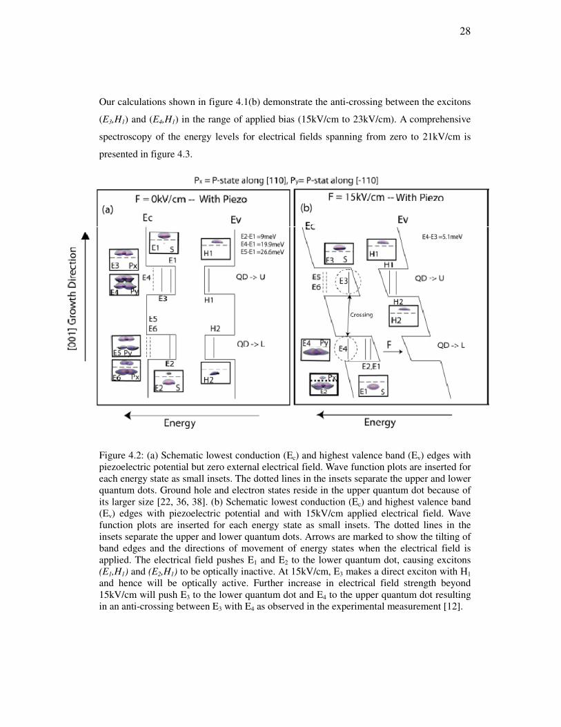
28
Our calculations shown in figure 4.1(b) demonstrate the anti-crossing between the excitons
(E3,H1) and (E4,H1) in the range of applied bias (15kV/cm to 23kV/cm). A comprehensive
spectroscopy of the energy levels for electrical fields spanning from zero to 21kV/cm is
presented in figure 4.3.
Figure 4.2: (a) Schematic lowest conduction (Ec) and highest valence band (Ev) edges with
piezoelectric potential but zero external electrical field. Wave function plots are inserted for
each energy state as small insets. The dotted lines in the insets separate the upper and lower
quantum dots. Ground hole and electron states reside in the upper quantum dot because of
its larger size [22, 36, 38]. (b) Schematic lowest conduction (Ec) and highest valence band
(Ev) edges with piezoelectric potential and with 15kV/cm applied electrical field. Wave
function plots are inserted for each energy state as small insets. The dotted lines in the
insets separate the upper and lower quantum dots. Arrows are marked to show the tilting of
band edges and the directions of movement of energy states when the electrical field is
applied. The electrical field pushes E1 and E2 to the lower quantum dot, causing excitons
(E1,H1) and (E2,H1) to be optically inactive. At 15kV/cm, E3 makes a direct exciton with H1
and hence will be optically active. Further increase in electrical field strength beyond
15kV/cm will push E3 to the lower quantum dot and E4 to the upper quantum dot resulting
in an anti-crossing between E3 with E4 as observed in the experimental measurement [12].
29
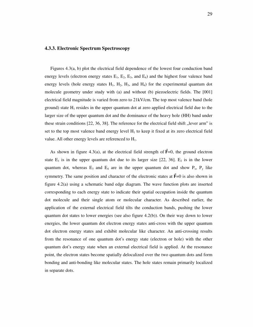
4.3.3. Electronic Spectrum Spectroscopy
Figures 4.3(a, b) plot the electrical field dependence of the lowest four conduction band
energy levels (electron energy states E1, E2, E3, and E4) and the highest four valence band
energy levels (hole energy states H1, H2, H3, and H4) for the experimental quantum dot
molecule geometry under study with (a) and without (b) piezoelectric fields. The [001]
electrical field magnitude is varied from zero to 21kV/cm. The top most valence band (hole
ground) state H1 resides in the upper quantum dot at zero applied electrical field due to the
larger size of the upper quantum dot and the dominance of the heavy hole (HH) band under
these strain conditions [22, 36, 38]. The reference for the electrical field shift „lever arm‟ is
set to the top most valence band energy level H1 to keep it fixed at its zero electrical field
value. All other energy levels are referenced to H1.
As shown in figure 4.3(a), at the electrical field strength of ��=0, the ground electron
state E1 is in the upper quantum dot due to its larger size [22, 36]. E2 is in the lower
quantum dot, whereas E3 and E4 are in the upper quantum dot and show Px, Py like
symmetry. The same position and character of the electronic states at ��=0 is also shown in
figure 4.2(a) using a schematic band edge diagram. The wave function plots are inserted
corresponding to each energy state to indicate their spatial occupation inside the quantum
dot molecule and their single atom or molecular character. As described earlier, the
application of the external electrical field tilts the conduction bands, pushing the lower
quantum dot states to lower energies (see also figure 4.2(b)). On their way down to lower
energies, the lower quantum dot electron energy states anti-cross with the upper quantum
dot electron energy states and exhibit molecular like character. An anti-crossing results
from the resonance of one quantum dot’s energy state (electron or hole) with the other
quantum dot’s energy state when an external electrical field is applied. At the resonance
point, the electron states become spatially delocalized over the two quantum dots and form
bonding and anti-bonding like molecular states. The hole states remain primarily localized
in separate dots.

30
The separation between the anti-crossings provides a direct measurement of the energy
levels of the lower quantum dot, and hence enables „reverse engineering‟ to determine the
quantum dot dimensions and symmetry. Such spectroscopic probing of the hole energy
states in a quantum dot molecule has been done recently [37] and is referred to as „level
anti-crossing spectroscopy‟. Figure 4.3(a) shows the distribution of three anti-crossings
(E1↔E2, E2↔E3, and E3↔E4) between the electron energy levels. At ��=0, E1 is in the upper
quantum dot and E2 in the lower quantum dot. The first anti-crossing E1↔E2 results from
the resonance of the two s-type electronic states E1 and E2 when the electrical field is in the
range of ~5kV/cm. The anti-crossing energy for E1↔E2 is ~5.9meV. For electrical fields
between 6kV/cm and 15kV/cm, E1 resides in the lower quantum dot and E2 resides in the
upper quantum dot. Increasing the electrical field up to ~15kV/cm results in a second anti-
crossing E2↔E3 between the s-type upper quantum dot state (E2) and the p-type lower
quantum dot state (E3). The anti-crossing energy for this s-p anti-crossing (~0.7meV) is
much smaller than the previous s-s anti-crossing energy. This anti-crossing involves states
that are higher in energy as measured from the relative bottom of the quantum well. The
barrier height that separates/couples the states is noticeably smaller. As such, the reduced
coupling strength is at first unintuitive.
The magnitude of the anti-crossing energy depends on the wave function overlap and the
symmetries of the states involved [37]. The s-p anti-crossing energy will be smaller than the
s-s anti-crossing energy because of the different spatial symmetries of the s- and p-states
and smaller overlap between these two orbitals. Beyond ��=15kV/cm, both E1 and E2 are
atomic like states confined in the lower quantum dot. Further electric field induced shifts
will bring E4 (lower quantum dot state) into resonance with E3 (upper quantum dot state)
and induce a third anti-crossing E3↔E4 between the s-type upper quantum dot state and the
p-type lower quantum dot state. The anti-crossing energy for E3↔E4 is ~1.1meV. Since the
experiment [12] was performed for electrical fields varying from 15kV/cm to 21kV/cm, the
only experimentally observed anti-crossing (see figure 4.1(b)) is E3↔E4.
31
32
Figure 4.3: (a, b) Plot of first four electron and hole energy levels as a function of applied
[001] electrical field. The electrical field is varied from zero to 21kV/cm. The H1 energy is
taken as the center of the electrical field lever arm so that its energy remains fixed at its
zero electrical field value. Wave functions are inserted as small insets at critical values of
electrical field to highlight the spatial position of the energy states inside the quantum dot
molecule. The dotted lines in the wave function insets are marked to guide the eyes and
separate the upper and lower quantum dots. Both electron and hole energy levels of the
lower quantum dot exhibit anti-crossings with the energy levels of the upper quantum dot.
The sequence of anti-crossings reveals the electron and hole level structure of the lower
quantum dot and provides a direct measurement of the energy states in the lower quantum
dot. The regions of the experimental electrical fields (from 15kV/cm to 21kV/cm) are
enlarged in figure 4.3 c and d.

33
The strength of the electrical field induced shift in the lower quantum dot energies
depends on the separation between the quantum dots, as the center of the electrical field
lever arm shift is fixed at H1 in the upper quantum dot. The slope of this shift, calculated
from figure 4.3(a), is ∆E/∆F ~ -1.33 meV kV-1
cm. This predicts the spatial separation
between H1 and the lower quantum dot electron states to be around 13.3nm. Since the
wetting layer separation is 10nm, the center-to-center distance between the quantum dots is
11.5nm. The small difference of 13.3-11.5=1.8nm between the predicted value and the
center-to-center distance of the quantum dots is due to the spatial separation between the
electron and hole states in the quantum dot. The hole states tend to reside closer to the top
of the quantum dot and the electron states closer to the bottom of the quantum dot [33].
This is also consistent with the slope of upper quantum dot electron energy shift, which is
around ∆E/∆F ~ -0.167 meV kV-1
cm. This corresponds to an intra-dot electron-hole spatial
separation of 1.67nm, close to the value of 1.8nm mentioned above.
The spectrum shown in figure 4.3(a) clearly shows the spectroscopic probing of the
lower quantum dot electron states by the upper quantum dot state E1. This technique is very
useful to determine the geometry parameters of the molecular quantum dot. For example, if
we do not know the separation between the quantum dots, the E1↔E2 anti-crossing values
of � and the slope of the energy shifts can be used to estimate the separation between the
quantum dots. Regarding the quantum dot molecule in this study, E4-E1 is ~19.9meV as
shown in figure 4.2(a) at �� =0. The anti-crossing between these two states occurs at
~18.3kV/cm. This gives approximately a separation of 10.87nm between the two quantum
dots, which is very close to the value of ~10nm provided by the TEM measurements [12].
Thus, the spacing between the anti-crossings and the electrical field induced stark shift
allow us to „reverse engineer‟ the separation between the quantum dots.
34
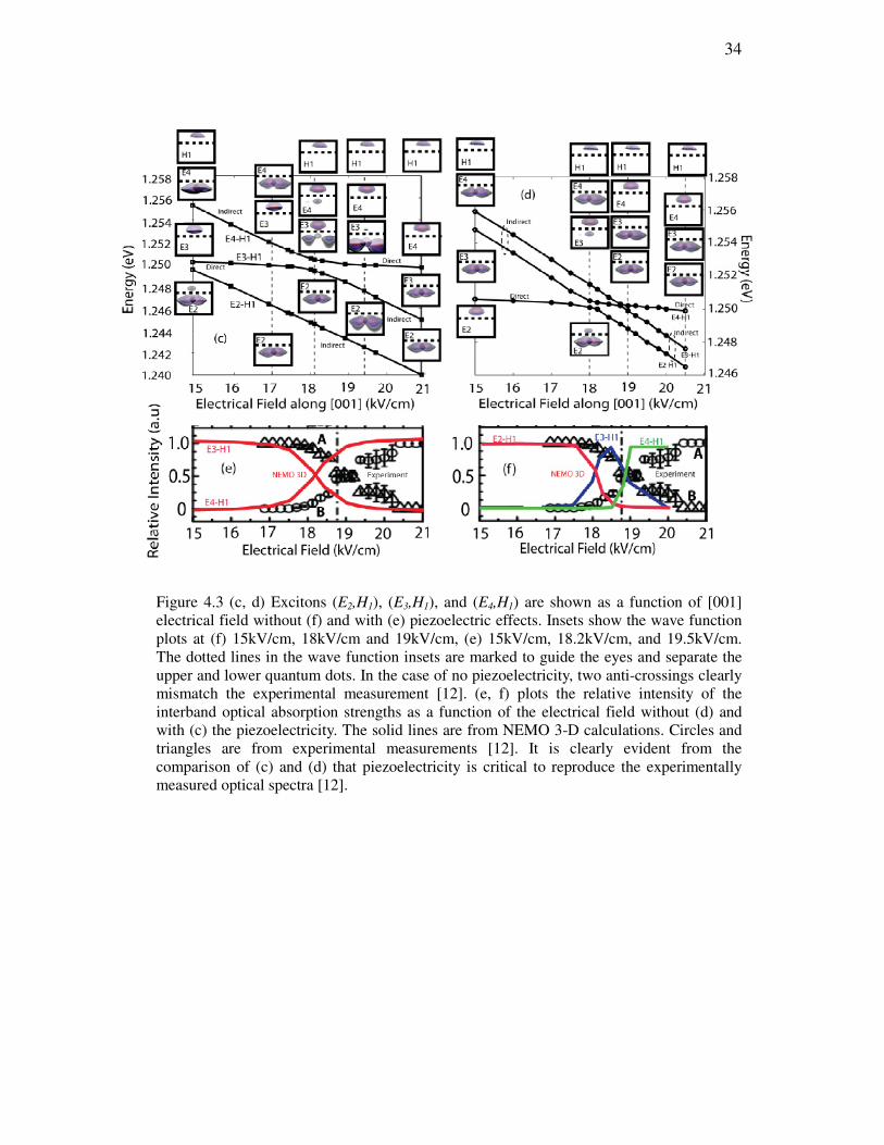
Figure 4.3 (c, d) Excitons (E2,H1), (E3,H1), and (E4,H1) are shown as a function of [001]
electrical field without (f) and with (e) piezoelectric effects. Insets show the wave function
plots at (f) 15kV/cm, 18kV/cm and 19kV/cm, (e) 15kV/cm, 18.2kV/cm, and 19.5kV/cm.
The dotted lines in the wave function insets are marked to guide the eyes and separate the
upper and lower quantum dots. In the case of no piezoelectricity, two anti-crossings clearly
mismatch the experimental measurement [12]. (e, f) plots the relative intensity of the
interband optical absorption strengths as a function of the electrical field without (d) and
with (c) the piezoelectricity. The solid lines are from NEMO 3-D calculations. Circles and
triangles are from experimental measurements [12]. It is clearly evident from the
comparison of (c) and (d) that piezoelectricity is critical to reproduce the experimentally
measured optical spectra [12].
35
The ground hole state H1 resides in the upper quantum dot as shown in figure 4.2,
regardless of the field strength. We therefore mark this state as the ground hole state of the
upper quantum dot: Hg→U. The electron ground state of the upper quantum dot is marked
as Eg→U and shown as a horizontal dotted line in figure 4.3(a). The optically active exciton
will always be comprised of these two ground states of the upper quantum dot. It should be
pointed out that, although Eg→U is referred to as the upper quantum dot ground state, this
energy state undergoes several anti-crossings with the lower quantum dot states and
exhibits both atomic and molecular character at increasing electrical field strengths. More
importantly, at the anti-crossing point E3↔E4, the Eg→U state hybridizes with the lower
quantum dot P-state. This is very critical, because it underlines the importance of
piezoelectric fields. As will be shown later, piezoelectricity has stronger effects on electron
P-states as compared to electron s-states.
Figure 4.3(a) also depicts the distribution of the hole energy level anti-crossings as a
function of the applied electrical field. The electric field pushes the hole energy levels of
the lower quantum dot further to lower energy values. Thus, by sweeping through the
electric field, we can obtain a spectroscopic image of the upper quantum dot’s hole energy
levels when these anti-cross with the hole energy levels of the lower quantum dot. H1 is in
the upper quantum dot at zero electric field and remains so for the applied electric field
direction. H2 is in the lower quantum dot and as it moves down in energy, it couples with
hole states in the upper quantum dot. This gives rise to the anti-crossings H2↔H3 and
H3↔H4. The hole anti-crossing energies are ~0.2meV and ~0.1meV for H2↔H3 and
H3↔H4 respectively. These hole anti-crossing energies are significantly smaller than the
corresponding electron anti-crossing energies, indicating a much stronger hole localization.
Notably, in the range of the experimental electric field from 15kV/cm to 21kV/cm, all of
the four hole levels are in the upper quantum dot and no anti-crossings are observed. This
implies that the electron states in the lower quantum dot exhibit weak optical transition
strengths with the first four hole energy levels and hence are not measured experimentally.
36
5. IMPACT OF PIEZOELECTRICITY
5.1. Energy Spectrum Without and With Piezoelectricity
The comparison of figures 4.3(a) and 4.3(b) highlights the impact of piezoelectric fields
on the energy spectrum of the quantum dot molecule under study. Piezoelectricity does not
impact the hole energy spectrum significantly. The hole energy levels exhibit only a small
energy shift and only minor changes are observed in the hole anti-crossings. The electron
ground state energies of the two quantum dots E1 and E2 and the anti-crossing E1↔E2 are
also only shifted by a small amount. However, the excited electron states E3 and E4 are
affected significantly.
Piezoelectricity increases the splitting between E3 and E4 and thus changes the position
of the anti-crossing E2↔E3 on the electrical field axis. With piezoelectricity considered,
E2↔E3 occurs outside the range of the experimentally applied electrical field. On the other
hand, if piezoelectricity is included, the anti-crossing E2↔E3 occurs within the range of the
experimentally applied electrical field. It implies that, without piezoelectric fields included,
there will be two anti-crossings in the range of the electric field from 15kV/cm to 21kV/cm.
This contradicts the experimental measurements shown in figure 4.1(b). To further explain
the anti-crossings in the experimental range of applied electric field, the two excitonic
spectra for both cases are enlarged in figure 4.3 c) and d).
Figures 4.3 (c, d) show the three exciton energies (E2,H1), (E3,H1), and (E4,H1) of the
system with (c) and without (d) piezoelectric potential considered as a function of applied
electric field. The wave functions of H1 as well as E2, E3, E4 are depicted as insets for a
number of electric field strengths. If both the electron and hole states are in the same
quantum dot, the resulting exciton is called a “direct exciton”. It corresponds to an optically
active state with a large electron hole overlap. On the other hand, if the electron and hole
states are in different quantum dots, the resulting exciton is called an “indirect exciton”. It
corresponds to an optically inactive state with a negligible electron and hole overlap.

37
Energy perturbations due to the Quantum Confined Stark Effect (QCSE) in direct and
indirect excitons under applied bias exhibit different slopes: ∆������ = . ��, where p is
the dipole moment of the exciton, and �� is the applied electric field. The exciton dipole
moment is defined as: p = q.d, where „q‟ is the electronic charge and „d‟ is the spatial
electron-hole separation. In the case of a direct exciton, both electron and hole are in the
same quantum dot and separated by a short distance (typically d ≤ 1nm). The resulting
magnitude of the Stark shift is therefore very small. In the case of an indirect exciton
however, the electron and hole are in different quantum dots and separated by a large
spatial distance (d ≥ 10nm in our case). Therefore, the dipole moment and the magnitude of
the Stark shift will be large. [33] Figure 4.3 (c) and (d) depict the direct and indirect nature
of the observed excitons over the range of applied bias. As the figures indicate, a strong
(larger slope) and a weak (smaller slope) Stark effect correspond to an indirect and direct
exciton, respectively.
The experimentally measured optical spectra (circles and triangles in figures 4.3(e) and
3(f)) show the relative strength of the two excitonic emissions ‘A’ and ‘B’. At �� =15kV/cm,
the excitonic emission ‘A’ is bright and ‘B’ is dark. As the electric field is increased, the
intensity of ‘A’ decreases and the intensity of ‘B’ increases. The optical strengths of both
excitons ‘A’ and ‘B’ become comparable at the electric field value of 18.8kV/cm, where
these two excitons anti-cross. At higher electric field strengths, the intensity of ‘A’
decreases rapidly and ‘B’ becomes optically bright.
We compute the transition rate intensities using Fermi’s golden rule as the squared
absolute value of the momentum matrix: |< ������|����, ��|�� > |�, where H is the single
particle tight binding Hamiltonian, E2or3or4 are electron states, H1 is the top most valence
band hole state, and ��� is the polarization direction of the incident light [32, 39-41]. Figure
4.3(e) compares the relative transition rate intensities � !",#$%�(!',#$)/(�(!",#$) +�(!' ,#$)), where �(!",#$) and �(!',#$)are the transition rate intensities of (E4,H1) and (E3,H1) ,
respectively.

38
Figure 4.3(f) compares the relative transition rate intensities �(!+,#$),-� !',#$%,-�(!",#$)/(�(!",#$) + �(!',#$) + �(!+,#$)) , where �(!+,#$), �(!',#$) and �(!",#$) are the transition rate
intensities of (E2,H1) , (E3,H1) and (E4,H1), respectively. Figure 4.3(e) compares the
calculated optical strengths, including piezoelectric effects, obtained from NEMO 3D with
the experimental measurements. In this case, as the electric field is increased, the intensity
of (E3,H1) reduces rapidly, whereas the intensity of (E4,H1) increases.
Figure 4.3(c) plots the excitonic energies (E2,H1), (E3,H1) and (E4,H1) as a function of
the applied electrical field. E2, which is localized in the lower dot, forms an indirect exciton
with H1 in the range of applied electric field from 15kV/cm to 21kV/cm. The optical
strength of (E2,H1) is therefore weak and not experimentally measured. On the contrary,
(E3,H1) is a direct exciton at 15kV/cm and experimentally measured as a strong optical peak.
Increasing the electric field from 15KV/cm results in the tunneling of E3 from the upper
quantum dot to the lower quantum dot. (E3,H1) eventually changes its character from an
optically active state to an optically inactive state at F~18.8kV/cm. In the vicinity of the
anti-crossing point (F from ~17.9kV/cm to ~20.5kV/cm), the two excitons (E3,H1) and
(E4,H1) are tuned into resonance and exhibit a close to equal magnitude of intensity. In that
field range, the electron states (E3 and E4) are found to be delocalized across the two
quantum dots. Note that the relative intensities of the excitons in figure 4.3(e) calculated by
our model closely follow the slopes of the experimental curves. NEMO 3-D is hence able
to correctly capture the dynamics of controlled coupling under resonance of excitons. The
controlled coupling of quantum dots under external bias (gate voltage) is critical in the
implementation of exciton qubits and may foster efforts in quantum information processing
based on quantum dots.

39
Figure 4.3(f) compares the experimentally measured transition strengths (‘A’ and ‘B’)
with our calculated transition strengths (solid lines) obtained from NEMO 3-D. Note that in
this case, we explicitly did not include piezoelectric effects. The calculated transition
strengths indicate three bright peaks and two anti-crossings. At F =15kV/cm, exciton (E2,H1)
is bright and excitons (E3,H1) and (E4,H1) are dark. As the electric field increases, first
(E2,H1) anti-crosses with exciton (E3,H1). Further increase in the electric field results in a
subsequent anti-crossing between excitons (E3,H1) and (E4,H1). Figure 4.3(d) plots the
corresponding excitonic energies as a function of applied electrical field. The direct and
indirect nature of the excitons follows the optical transition strength patterns of figure
4.3(d). At =15kV/cm, exciton (E2,H1) is direct and excitons (E3,H1) and (E4,H1) are indirect.
The first anti-crossing makes exciton (E2,H1) indirect and exciton (E3,H1) direct. The
second anti-crossing makes exciton (E3,H1) indirect and exciton (E4,H1) direct. In short, the
omission of piezoelectricity, as shown in the figures 4.3(d) and 4.3(f), results in three bright
excitonic emissions, which disagrees with the experimentally measured spectra.
The anti-crossings of the electron states in the experimental electric field range involve
electron P-states of the lower quantum dot. Since piezoelectric effects are more pronounced
in excited states [23-26, 28, 29, 38], the correct identification of optically active states in
the experimental measurements is of crucial importance. If the experimental emissions
came from the ground state, piezoelectric effects would be of minor. Figures 4.3(c) and
4.3(d) clearly show that including piezoelectric effects is important to obtain the correct
resonance at the point of anti-crossing. Furthermore, the field dependence of the optical
intensity is also strongly dependent on piezoelectricity. We obtain the smoothly varying
intensity variation as obtained in the experiment only when piezoelectric fields are included
[12].
40
5.2. Piezoelectric Model
Piezoelectricity is calculated from electrical polarization originating from stressed
crystals lacking inversion symmetry [29]. InGaAs/GaAs quantum dots are nanostructures
with a lattice mismatch (~7%), which leads to long-range strain fields penetrating deep into
the surrounding buffer [22, 27, 38]. The diagonal and off-diagonal (shear) strain
components can result into a built-in piezoelectric polarization, which cannot be ignored.
Bester et al. [24] and Ahmed et al. [27] outlined the importance of linear piezoelectric
effects for single InAs quantum dots. Later, Bester et al. [25] highlighted the significance
of the second order (quadratic) component of piezoelectricity. They concluded that the
second order piezoelectric effect cancels the first order (linear) component, thus leading to
a net piezoelectric effect significantly suppressed. Following their argument that the net
piezoelectric effect and its impact on the excitonic spectrum is negligible, they further
claimed that it is advisable not to consider piezoelectric effects at all rather than including
only the linear component of the piezoelectric effect.
On the other hand, Schliwa et al. [28, 29] have indicated the importance of net
piezoelectricity for a number of shapes and sizes of single quantum dots. The work
presented here on quantum dot molecules clearly emphasizes that net piezoelectric effects
cannot be neglected and are of critical importance in determining correct excitonic emission
spectra in coupled dot systems that involve occupation of excited states.
In our model, the piezoelectric potential is included into the single particle Hamiltonian
according to the recipe presented in references [24, 29]. First, both linear P1 (first order)
and quadratic P2 (second order) polarizations are separately calculated from the strain
tensor components (equations (1) and (2)) using already published polarization constants
(e14, β114, β124, β156) (See table 1) [24, 25]. They are then added to calculate the total
polarization P=P1+P2:

41
./ = 21�� 23453�53�46 (1)
.7 = 8��� 23��3453443�53553�46 + 8��� 9345(344 + :55)3�5(355 + :��)3�4(3�� + :44); + 8�<= 23�53�43453�43453�56 (2)
The divergence of the total polarization P is calculated over a rectangular mesh using a
finite difference approach to calculate total charge density ρ(r):
>(?) = −∇. . (3)
Finally, the Poisson equation (4) is solved to calculate the piezoelectric potential Vp(r),
taking into account the position dependence of the static dielectric constant, ɛs(r). The value
of the dielectric constant for vacuum ɛ0 is 8.85x10⁻¹²F/m. For InGaAs and GaAs materials,
we used the relative dielectric constant values of 14.0ɛ0 and 12.84ɛ0, respectively.
B(?) = :C∇. �:D(?) ∇ EF(?)� (4)
5.3. Quadrupole Nature of the Piezoelectric Potentials
Figure 5.1(a) shows the first order (solid line with square), the second order (dashed
line), and the sum of the first and second order (solid line with circle) piezoelectric
potentials along the [001] direction through the center of the quantum dot molecule. It is
evident that the net piezoelectric potential is nonzero inside the quantum dot and penetrates
into the surrounding GaAs buffer. The reason for the nonzero net potential inside the
quantum dot is that the quadratic (second order –> dashed line) component of the potential
is significantly reduced for alloyed quantum dots (In0.5Ga0.5As) due to the following reasons:
(1) Increasing the „Ga‟ concentration reduces the diagonal strain components that
determine the quadratic component.

42
(2) The polarization constant B124, which comprises a major portion of the quadratic
component is reduced in magnitude. The linear (first order –> solid line with square)
component, on the other hand, increases mainly due to the large increase of e14. The
reduced quadratic component cannot cancel the effect of the already enhanced linear
component, and hence the interior of the quantum dot will have a nonzero potential largely
dominated by the linear component (see the solid line with circle). Outside of the quantum
dot, the quadratic component is negligible, and only the linear component is dominant. As a
result, the net piezoelectric effect inside and at the interfaces of the quantum dots is no
longer found to be negligible.
Polarization Constant Type of Component GaAs (C/m2) InAs (C/m
2) In0.5Ga0.5As (C/m
2)
e14 Linear (Experiment) -0.16 -0.045 -0.1025
e14 Linear (Calculated) -0.23 -0.115 -0.1725
B114 Quadratic (Calculated) -0.439 -0.531 -0.485
B124 Quadratic (Calculated) -3.765 -4.076 -3.9205
B156 Quadratic (Calculated) -0.492 -0.12 -0.306
Table 1: Polarization constants for calculation of piezoelectric potential from reference [24].
The values for In0.5Ga0.5As are obtained by linear interpolation between GaAs and InAs.

43
Figure 5.1: (a) The first order (line with the box), second order (dashed line) and the sum
of first and second order (line with the circle) piezoelectric potential are shown through the
center of the quantum dot along the [001] growth direction. The net potential is clearly
nonzero inside the quantum dots, at the interfaces of the quantum dot and in the
surrounding buffer. The second order piezoelectric effect is weak and cannot cancel the first
order effect inside the quantum dot. (b, c) Piezoelectric potential plotted through the center
of the upper quantum dot in the [110] and [1H10� directions. The origin of the x-axis is taken
at the center of the quantum dot. The quadrupole nature of the potentials is clearly evident:
the potential is positive at the interface of the quantum dot and buffer along the [110]
direction, whereas it is negative at the interface of the quantum dot and buffer along the
[1H10� direction. The random nature of the potential inside the quantum dot region is a result
of the random alloy configuration of the In0.5Ga0.5As quantum dot material. The quadrupole
nature of the piezoelectric potential along diagonal directions strongly affects the splitting
and orientation of the electron P-states, which are aligned along these directions due to
atomistic asymmetry. (d, e) The two dimensional (xy) contour plots of the net piezoelectric
potential at the base of the lower and upper quantum dots are shown as a function of
distance along the [100]- and [010]-axis. The quadrupole nature of the potential is clearly
evident from the plots. Furthermore, the potential is long ranged and penetrates deep inside
the GaAs buffer.

44
Figures 5.1(b,c) show the net piezoelectric potential along the diagonal [110] and �1H10�directions through the center of the upper quantum dot. Figure 5.1(d, e) show the two
dimensional contour plots of the net piezoelectric potentials about 1nm above the base of
the lower and upper quantum dots. The quadrupole nature of the net piezoelectric potentials
along the diagonal directions is clearly evident. The piezoelectric potentials along the [110]
and �1H10� directions are large at the interfaces, where strain is large and penetrates deep
into the GaAs buffer [26, 27]. A large GaAs buffer is therefore not only required along the
[001] direction, but also in the plane of the quantum dot to fully capture the effect of the
piezoelectric potential reaching 25-30nm deep into the GaAs buffer. The wide extension of
the piezoelectric fields in the lateral plane also implies that the quantum dots that are closer
than ~30 nm will interact with each other through the piezoelectric potentials.
Past studies [26-29] have shown that the quadrupole nature of the piezoelectric effect
significantly changes the splitting and orientation of electron P-states, which are already
oriented along diagonal directions due to atomistic interface and strain asymmetry. In figure
4.1(b), the optically active states in the experimental spectrum are identified as excited
states (E3 and E4) in the range of applied bias. The next paragraph shows that considering
piezoelectric effects is indeed critical in reproducing the experimental excitonic spectrum.
5.4 Quantitative Explanation of ‘One’ vs. ‘Two’ Anti-Crossings
Figure 5.2 presents a quantitative explanation of the presence of ‘one’ and ‘two’ anti-
crossings. It shows a flow diagram in two directions: (Flow to right) First six electron states
without piezoelectricity and without electrical field à with piezoelectricity but without
electrical field à with piezoelectricity and with electric field of 15kV/cm. (Flow to left)
First six electron states without piezoelectricity and without electrical field à without
piezoelectricity and with electric field of 15kV/cm. It is critical to investigate the
arrangement of the electron states at 15kV/cm to understand the resonance behavior at
higher electric field values.
45
Since the first hole state remains in the upper quantum dot throughout the sweeping process
of the electrical field, it is not included in figure 5.2. Piezoelectricity shifts the ground
electron state E1(U-S) only by a very small value of 0.59meV. The major contribution
towards the shifting of the ground electron state comes from the externally applied bias.
Hence, the total shift in this state in either direction is approximately the same:
Left=15.09meV, Right=15.01+0.59=15.6meV. The most significant effect of the
piezoelectric effect is found to be on the E5(L-Px) and E6(L-Py) electron states. These states
are not only shifted by a larger magnitude, but also their relative order is changed.
Similar behavior has been observed in previous studies for a single quantum dot [25-27,
29], in which a strong piezoelectric effect has been shown to flip the order of the electron
P-states. Here, the piezoelectric effect induces a shift of 0.7meV and 3.2meV in E5(L-Px)
and E6(L-Py) respectively, followed by an additional electric field induced shift of 7.7meV
and 11.5meV respectively. This total shift of 3.2+11.5=14.7meV causes E6(L-Py) to become
E2(L-Py) at 15kV/cm, which is below E3(U-S) on the same energy scale. A further increase
of the electrical field beyond 15kV/cm will shift E3(U-S) to higher energies and E4(L-Px) to
lower energies. This will result in a resonant coupling of these two states with one anti-
crossing (E3 à E4) in the emission spectra. Going in the left direction according to figure
5.2 with no piezoelectricity included, there will be no additional shift of 3.2meV and
0.7meV in the lower quantum dot P-states. Mere electric field induced shifts of 10.02meV
and 10.11meV are not sufficient enough to push either of the two excited states below
E2(U-S). This results in the observation of two anti-crossings (E2 à E3 à E4).

46
Figure 5.2: Flow diagram showing the arrangement and position of the first six electron
states in the conduction band of the quantum dot molecule. Piezoelectric effects reorder the
P-states in the lower quantum dot and play a critical role in determining the resonances
occurring at higher electric field strengths.
47

6. CONCLUSIONS
In this work, we presented a detailed systematic atomistic tight binding study of an
experimental single quantum dot molecule geometry, taking into account long range strain,
atomistic interface asymmetry, and both linear and the quadratic piezoelectric effects. The
quantum dot molecule energy states are composed of individual single quantum dot states,
which can interact with each other depending on their energetic alignment. The external
electrical field enables tuning of the relative alignment of molecular and atomic states,
which has been observed in experimental spectroscopy data [12]. Our calculations
quantitatively reproduce the experimental spectra. The interband transition strengths are
calculated to compare the relative intensities of the excitonic emissions and to characterize
them as either optically active or inactive states. The calculated transition strengths closely
follow the experimentally measured intensities and identify the excited electron (P-states)
states as the optically active states in the range of the applied electrical field. The close
quantitative agreement of our theoretical calculations with the experimental data [12]
allows us to gain significant physical insight of the investigated quantum dot molecule. We
sweep the electrical field from zero to 21kV/cm and provide a spectroscopic mapping of
the lower quantum dot electron states and the upper quantum dot hole excited states.
Analysis of the observed sequence of anti-crossings provides a technique to precisely probe
the energy states of one quantum dot with the help of the energy states of the neighboring
quantum dot. The direction of the applied electrical field determines the quantum dot
whose electron/hole electronic states will be probed by increasing the electrical field
magnitude. This technique can be used to „reverse engineer‟ the geometry of the quantum
dot molecule from the experimentally measured optical spectrum.
The strain and piezoelectric fields are both found to be long range effects. This imposes
the need of a large simulation domain size consisting of about 15 million atoms in the strain
domain and about 9 million atoms in the electronic domain. Our calculations include both
first order and second order piezoelectric fields. The quadrupole nature of the net
piezoelectric effect along [110] and �1H10� directions significantly affects the splitting and
orientation of the excited electron states.

48
The NEMO 3-D based atomistic study shows that the net piezoelectric effect is critical in
reproducing the experimentally observed optical transitions. Continuum methods such as
the effective mass model and k•p method do not take into account the atomistic nature of
the InGaAs quantum dots and thus cannot correctly incorporate the strain and piezoelectric
fields.
Major parts of the work presented in this thesis are currently under review for publication
in ACS Nano.
Quantitative Excited State Spectroscopy of a Single InGaAs Quantum Dot Molecule through Multi-
million Atom Electronic Structure Calculations
Muhammad Usman, Yui Hong Matthias Tan, et al. http://arxiv.org/abs/1008.3127
49
LIST OF REFERENCES
[1] P. Michler, “Single Quantum Dot”, Springer, Berlin, 2003
[2] D. Bimberg, “Semiconductor Nanostructures”, Springer Berlin, 2008; D. Bimberg, M.
Grundmann, and N. N. Ledentsov, “Quantum Dot Heterostructures”, John Wiley & Sons,
Chichester, 1999;
[3] N. H. Bondeo, J. Erland, D. Gammon, D. Park, D. S. Katzer and D. G. Steel, Science
282, 1473, 1998
[4] Xiaoqin Li et al., Science 301, 809, 2003
[5] D. Loss and D. P. DiVincenzo, Phys. Rev. A 57, 120, 1998.
[6] W. G. van der Wiel, S. D. Franceschi, J. M. Elzerman, T. Fujisawa, S. Tarucha, and L.
P. Kouwenhoven, Rev. Mod. Phys. 75, 1, 2003
[7] O. Gywat, G. Burkard, and D. Loss, Superlattices and Microstrctures 31, 127, 2002.
[8] X. Q. Li and Y. Arakawa, Phys. Rev. A 63, 012302, 2000.
[9] B. W. Lovett, J. H. Reina, A. Nazir, and G. A. Briggs, Phys. Rev. B 68, 205319, 2003.
[10] T. H. Oosterkamp et al., Nature 395, 873, 1998.
[11] M. Bayer et al., Science 291, 451, 2001.
[12] H. J. Krenner, M. Sabathil, E.C. Clark, A. Kress, D. Schuh, M. Bichler, G. Abstrieter,
and J.J. Finely, “Direct observation of controlled coupling in an individual quantum dot
molecule,” Phys. Rev. Lett. 94, 057402 (2005)
[13] G. Klimeck, S. Ahmed, H. Bae, N. Kharche, R. Rahman, S. Clark, B. Haley, S. Lee, M.
Naumov, H. Ryu, F. Saied, M. Prada, M. Korkusinski, and T.B. Boykin, “Atomistic
simulation of realistically sized Nanodevices using NEMO 3-D: Part I – Models and
Benchmarks,” (INVITED) Special issue on NanoElectronic device modeling in IEEE
Transactions Electron Devices, vol. 54, no. 9, pp. 2079-2089, Sep. 2007
[14] G. Klimeck, S. Ahmed, N. Kharche, M. Korkusinski, M. Usman, M. Prada, and T.B.
Boykin, “Atomistic simulation of realistically sized Nanodevices using NEMO 3-D: Part II
– Applications,” (INVITED) Special issue on NanoElectronic device modeling in IEEE
Transactions Electron Devices, vol. 54, no. 9, pp. 2079-2089, Sep. 2007
[15] G. Klimeck, F. Oyafuso, T.B. Boykin, R.C. Bowen, and P. V. Allmen, “Development
of a nanoelectronic 3-D (NEMO 3-D) simulator for multimillion atom simulations and its
application to alloyed quantum dots,” (INVITED) Computer Modeling in engineering and
Science (CMES), vol. 3 no.5, pp. 601-642 (2002)
50
[16] M. Usman, H. Ryu, I. Woo, D.S. Ebert, and G. Klimeck, “Moving towards Nano-
TCAD through multi-million atom quantum dot simulations matching experimental data”,
IEEE Trans. on Nanotechnology, vol. 8, No. 3, May 2009
[17] T.B. Boykin, G. Klimeck, R.C. Bowen, and F. Oyafuso, “Diagonal parameter shifts
due to nearest-neighbor displacements in empirical tight binding theory,” Physical rev. B
66, 125207 (2002)
[18] P. Keating, “Effect of invariance requirements on the elastic strain energy of crystal
with application to diamond structure,” Physical Rev. 145, no. 2, pp.737, May 1966.
[19] R. Rahman, C.J. Wellard, F.R. Bradbury, M. Prada, J.H. Cole, G. Klimeck, and L.C.L.
Hollenberg, “High precision quantum control of single donor spins in Si,” Phys. Rev. Lett.
99, 036403 (2007)
[20] G.P. Lansbergen, R. Rahman, C.J. Wellard, P.E. Rutten, J. Caro, N.cCollaert, S.
Biesemans, I. Woo, G. Klimeck, L.C.L. Hollenberg, and S. Rogge, “Gate induced quantum
confinement transition of a single dopant atom in a Si FinFET,” Nature Physics, vol. 4,
p.656 (2008)
[21] N. Kharche, M. Prada, T.B. Boykin, and G. Klimeck, “Valley-splitting in strained
Silicon quantum wells modeled with 2 degree miscut, step disorder and alloy disorder,”
Appl. Phys. Lett. 90, 092109 (2007)
[22] Muhammad Usman, Shaikh Ahmed, and Gerhard Klimeck, “Atomistic tight binding
study of strain-reduced confinement potentials in identical and non-identical InAs/GaAs
vertically stacked quantum dots,” in proc. of 8th IEEE NANO Arlington TX, August 2008,
pp. 541-544.
[23] G. Bester, X. Wu, D. Vanderbilt, and A. Zunger, “Importance of second-order
piezoelectric effects in zinc-blende semiconductors,” Phys. Rev. Lett. 96, 187602 (2006)
[24] G. Bester, A. Zunger, X. Wu, and D. Vanderbilt, “Effects of linear and nonlinear
piezoelectricity on the electronic properties of InAs/GaAs quantum dots,” Physical Rev. B
74, 081305(R) (2006)
[25] G. Bester and A. Zunger, “Cylindrically shaped zinc-blende semiconductor quantum
dots do not have cylindrical symmetry: Atomistic symmetry, atomic relaxation, and
piezoelectric effects,” Physical Rev. B 71, 045318 (2005)
[26] S. Islam, S. Sundaresan, and S. Ahmed, “Geometry dependence of the internal fields
and its impact on the electronic structure in self-assembled InAs/GaAs quantum dots,”
IEEE Trans. on Nanotechnology (under review)

51
[27] Shaikh Ahmed, Muhammad Usman, N. Kharche, Andrei Schliwa, and Gerhard
Klimeck, “Atomistic simulation of non-degeneracy and optical polarization anisotropy in
pyramidal quantum dots,” in proc. of IEEE NEMs, Bangkok Thailand, January 16-19, 2007,
pp.937-942
[28] A. Schliwa, M. Winkelnkemper, and D. Bimberg, “Few-particle energies versus
geometry and composition of InGaAs/GaAs self-organized quantum dots,” Physical Rev. B
79, 075443 (2009)
[29] A. Schliwa, M. Winkelnkemper, and D. Bimberg, “Impact of size, shape, and
composition on piezoelectric effects and electronic properties of In(Ga)As/GaAs quantum
dots,” Physical Rev B 76, 205324 (2007)
[30] L.R.C. Fonseca, J.L. Jimenez, and J.P. Leburton, “Electronic coupling in InAs/GaAs
self-assembled stacked double-quantum-dot systems,” Physical Rev. B 58, 9955 (1998-I)
[31] Olga L. Lazarenkova, P. von Allmen, F. Oyafuso, S. Lee, and G. Klimeck, “Effect of
anharmonicity of the strain energy on band offsets in semiconductor nanostructures,” Appl.
Phys. Lett. 85, 4193 (2004)
[32] Muhammad Usman, Hoon Ryu, Sunhee Lee, Yui H. Matthias Tan, and Gerhard
Klimeck, “Quantum confined stark shift and ground state optical transition rate in [100]
laterally biased InAs/GaAs quantum dots” IEEE proceedings of 13th International
workshop on computational electronics IWCE China, May 27-29 (2009)
[33] P.W. Fry et al., Phys. Rev. Lett. 84, 733 (2000)
[34] M.F. Doty, J.I. Climente, A. Greilich, M. Yakes, A.S. Bracher, and D. Gommon,
“Hole spin mixing in InAs quantum dot molecule,” Physical Rev. B 81, 035308 (2010)
[35] D. Litvinov, H. Blank, R. Schneider, D. Gerthsen, T. Vallaitis, J. Leuthold, T. Passow,
A. Grau, H. Kalt, C. Klingshirn, and M. Hetterich, “Influence of InGaAs cap layers with
different In concentration on the properties of InGaAs quantum dots,” Journal of Appl.
Physics 103, 083532 (2008)
[36] Marek Korkusinski and Gerhard Klimeck, “Atomistic simulations of long-range strain
and spatial asymmetry molecular states of seven quantum dots”, Journal of Physics:
Conference Series, Vol. 38, pg. 75-78 (2006)
[37] M. Scheibner, M. Yakes, A.S. Bracker, I.V. Ponomarev, M.F. Doty, C.S. Hellberg, L.J.
Whitman, T.L. Reinecke, and D. Gammon, “Optically mapping the electronic structure of
coupled quantum dots”, Nature Physics, Vol. 4 pp. 291-295 (2008)

52
[38] Shaikh Ahmed, Neerav Kharche, Rajib Rahman, Muhammad Usman, Sunhee Lee,
Hoon Ryu, Hansang Bae, Steve Clark, Benjamin Haley, Maxim Naumov, Faisal Saied,
Marek Korkusinski, Rick Kennel, Michael McLennan, Timothy B. Boykin, Gerhard
Klimeck, "Multimillion Atom Simulations with NEMO 3-D" published in Springer
Encyclopedia for Complexity, 2008 (Full Paper at arXiv:0901.1890v1)
[39] Timothy B. Boykin and P. Vogl, “Dielectric response of molecules in empirical tight
binding theory”, Phys. Rev. B 65, 035202 (2001)
[40] Timothy B. Boykin, R. Chris Bowen, and Gerhard Klimeck, “Electromagnetic
coupling and gauge invariance in the empirical tight binding theory”, Phys. Rev B 63,
245314 (2001)
[41] M. Graf and P. Vogl, Phys. Rev. B 51, 4940 (1995)
[42] S. Lee, J. Kim, L. Jönsson, J. W. Wilkins, G. Bryant, and G. Klimeck,
“Many-body levels of multiply charged and laser-excited InAs nanocrystals modeled by
empirical tight binding,” Phys. Rev. B, Condens. Matter, vol. 66, p. 235 307, 2002.
[43] T. B. Boykin, G. Klimeck, R. C. Bowen, and F. Oyafuso, “Diagonal parameter shifts
due to nearest-neighbor displacements in empirical tight-binding theory,”
Phys. Rev. B, Condens. Matter, vol. 66, no. 12, p. 125 207, Sep. 2002.
[44] G. Klimeck, F. Oyafuso, T. Boykin, R. Bowen, and P. von Allmen, “Development of a
nanoelectronic 3-D (NEMO 3-D) simulator for multimillion atom simulations and its
application to alloyed quantum dots,” Comput. Model. Eng. Sci., vol. 3, p. 601, 2002.
[45] G. Klimeck, R. C. Bowen, T. B. Boykin, C. Salazar-Lazaro, T. A. Cwik, and A.
Stoica, “Si tight-binding parameters from genetic algorithm fitting,”
Superlattices Microstruct., vol. 27, no. 2/3, pp. 77–88, Mar. 2000.
[46] K. Eberl, “Quantum Dot lasers”, Physics World, Sept. 1997, p. 47-50
[47] D. Mowbray, M. Skolnick, “ New physics and devices based on self-assembled
semiconductor quantum dots”, J. Phys. D: Appl. Phys. 38 (2005)
[48] S. Li, Xia, J. Bai, “Quantum-confined Stark effects of InAs/GaAs self-assembled
quantum dot”, Journal of Applied Physics, Vol. 88, Issue 12, pp. 7171-7174 (2000)
[49] K. L. Janssens, B Partoens, F. M. Peeters, “Stark shift in single and vertically coupled
type-I and type-II quantum dots”, Physical Review B, Vol. 65, 233301, 2002
[50] S. Raymond, J.P. Reynolds, J.L. Merz, S. Fafard, Y. Feng, S. Charbonneau,
“Asymmetric Stark shift in AlxIn1-xAs/AlyGa1-yAs self-assembled dots”, Physical Review B,
Vol. 58, Nr. 20, 1998
Top Related