


Languages
Pages
Legal


ECE 4514Digital Design II
Spring 2008
Lecture 20:
Patrick SchaumontSpring 2008
ECE 4514 Digital Design IILecture 20: Timing Analysis
Lecture 20: Timing Analysis and
Timed Simulation
A Tools/Methods Lecture
Patrick Schaumont

Topics
� Static and Dynamic Timing Analysis
� Static Timing Analysis
� Delay Model
� Path Delay
� False Paths
� Timing Constraints
Patrick SchaumontSpring 2008
ECE 4514 Digital Design IILecture 20: Timing Analysis
� FPGA Design Flow & STA: Sorter Example
� Dynamic Timing Analysis
� FPGA Design Flow & Timed Simulation
� Delay back-annotation with SDF files
� Demonstration

Static and Dynamic Timing Analysis
� Suppose that we want to automatically find the maximum clock
DigitalSynchronous
Design
fCLK
Input Output
Patrick SchaumontSpring 2008
ECE 4514 Digital Design IILecture 20: Timing Analysis
� Suppose that we want to automatically find the maximum clock frequency of a given design
� written in Verilog
� and synthesized to a given technology
� Approach 1: Static Timing Analysis = use analysis techniques on the netlist to define fclk,max
� Approach 2: Dynamic Timing Analysis = use simulation and selected input stimuli to measure the slowest path

Static and Dynamic Timing Analysis
� Static Timing Analysis seems ideal, since it is done by a design tool that starts from the netlist and runs automatically
� However, Static Timing Analysis may report pessimistic results and report delays that will never occur during operation
� Dynamic Timing Analysis is nice, because we can combine it with the simulations which we do for functional verification
Patrick SchaumontSpring 2008
ECE 4514 Digital Design IILecture 20: Timing Analysis
� However, Dynamic Timing Analysis may be too optimistic, in particular if we do not simulate the worst possible case (which may be hard to predict in a complex netlist)
� In this lecture, we put the two techniques side-to-side

Static Timing Analysis
� STA looks for the worst of the following delays in a chip
Delay frominput toregister
Delay fromregister to
register
Delay fromregister to
output
Patrick SchaumontSpring 2008
ECE 4514 Digital Design IILecture 20: Timing Analysis
CombinationalLogic
CombinationalLogic
CombinationalLogicIN OUT

Static Timing Analysis
� STA relies on a similar model as we discussed before
CombinationalLogic
Patrick SchaumontSpring 2008
ECE 4514 Digital Design IILecture 20: Timing Analysis
Tclk,min = Tclk->Q + TLogic + TRouting + TSetup
CLK
Property ofthe component
(flipflop)
Property ofthe netlist
Property ofthe component
(flipflop)

Static Timing Analysis
� STA also takes delay on the clock connection into account. This is called clock skew.
� The effect of clock skew is highly dependent on circuit topology
CombinationalLogic
Patrick SchaumontSpring 2008
ECE 4514 Digital Design IILecture 20: Timing Analysis
Logic
Tclk,min = Tclk->Q + TLogic + TRouting + TSetup - TSkew
CLKTskew
Here, skew works'in favor' of us.

Static Timing Analysis
� STA also takes delay on the clock connection into account. This is called clock skew.
� The effect of clock skew is highly dependent on circuit topology
CombinationalLogic
Patrick SchaumontSpring 2008
ECE 4514 Digital Design IILecture 20: Timing Analysis
Logic
Tclk,min = Tclk->Q + TLogic + TRouting + TSetup + TSkew
CLK
Tskew
Here, skew works'against' us.

Static Timing Analysis
� STA also takes delay on the clock connection into account. This is called clock skew.
� The effect of clock skew is highly dependent on circuit topology
� the physical layout of the chip including the placement of components and the routing of wires
� The best clock skew is 0.
Patrick SchaumontSpring 2008
ECE 4514 Digital Design IILecture 20: Timing Analysis
� The best clock skew is 0.
� Chips will distribute the clock signal so that it arrives at every flip-flop at exactly the same moment

Static Timing Analysis
� So, once the technology is chosen, STA needs to find the longest combinational path, consisting of Tlogic + Trouting
� Path delay = delay from an input to an output. M inputs, N outputs -> M x N path delays possible
Combinational Logic
Patrick SchaumontSpring 2008
ECE 4514 Digital Design IILecture 20: Timing Analysis
Combinational Logic
10 ns
12 ns15 ns
9 ns
Worst case delay = 15ns

Delay of single path
� Path delay = Intrinsic Gate Delay + Fan-out Delay + Wire Delay
� Intrinsic Delay:
1 ns
Patrick SchaumontSpring 2008
ECE 4514 Digital Design IILecture 20: Timing Analysis
intrinsic delay = 1ns(delay of each gate
when not connected)
In
Out
Delay of a path
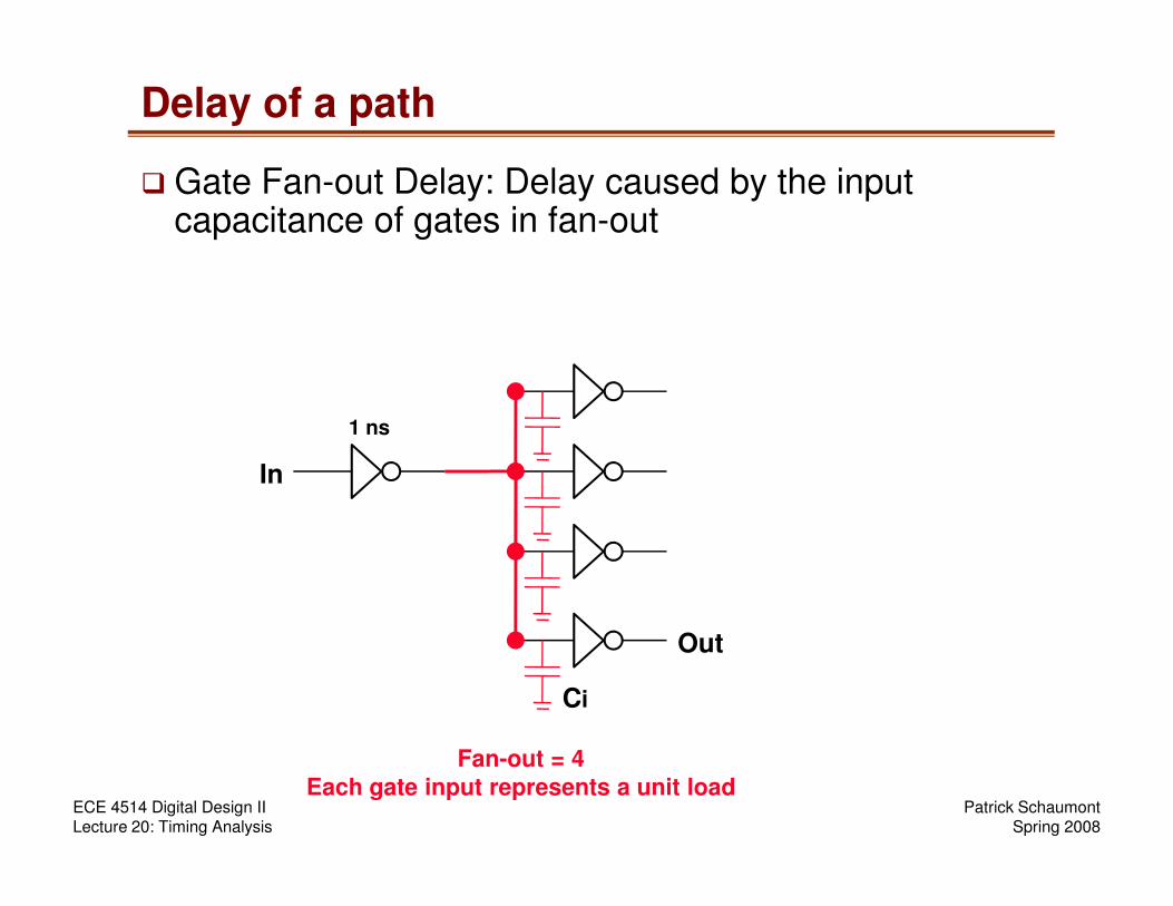
� Gate Fan-out Delay: Delay caused by the input capacitance of gates in fan-out
1 ns
Patrick SchaumontSpring 2008
ECE 4514 Digital Design IILecture 20: Timing Analysis
Fan-out = 4Each gate input represents a unit load
Ci
In
Out

Static Timing Analysis
� Gate Fan-out Delay:
� Ci = Capacitive load of a CMOS input
1 ns
V1 load
V V
Patrick SchaumontSpring 2008
ECE 4514 Digital Design IILecture 20: Timing Analysis
t
V
Fan-out
Delay
Vi,H
RC-delayR ~ drive capability of inverter output stageC ~ loading of output
CiVinput

Static Timing Analysis
� Gate Fan-out Delay:
� Appromated by N (fan-out) x D (delay per fan-out)
� Eg. a gate has 0.5 ns delay per fanout, then driving 3 gates will cost 1.5 ns delay
1 ns
V1 load
V V 3 load
Patrick SchaumontSpring 2008
ECE 4514 Digital Design IILecture 20: Timing Analysis
t
V
Delay
Vi,H
Ci
Vinput
3 load

Static Timing Analysis
� The path shown has 1ns + 2ns + 1ns = 4ns delay.
2 ns
Patrick SchaumontSpring 2008
ECE 4514 Digital Design IILecture 20: Timing Analysis
2 ns
4 x 0.5 ns
� After placement and routing has completed, additional correction factors can be included (delay of wires)

Static Timing Analysis
� STA may find paths that are never activated during operation. Such paths are called false paths
Select
Patrick SchaumontSpring 2008
ECE 4514 Digital Design IILecture 20: Timing Analysis
CombLogic
CombLogic
1
0
1
0

Static Timing Analysis
� STA may find paths that are never activated during operation. Such paths are called false paths.
� Designers must indicate such false paths to the STA tools (based on constraints)
Select
Patrick SchaumontSpring 2008
ECE 4514 Digital Design IILecture 20: Timing Analysis
Logic
Logic
1
0
1
0
Even though the red path has the longestdelay, it will never be triggered in practice.
This is a false path
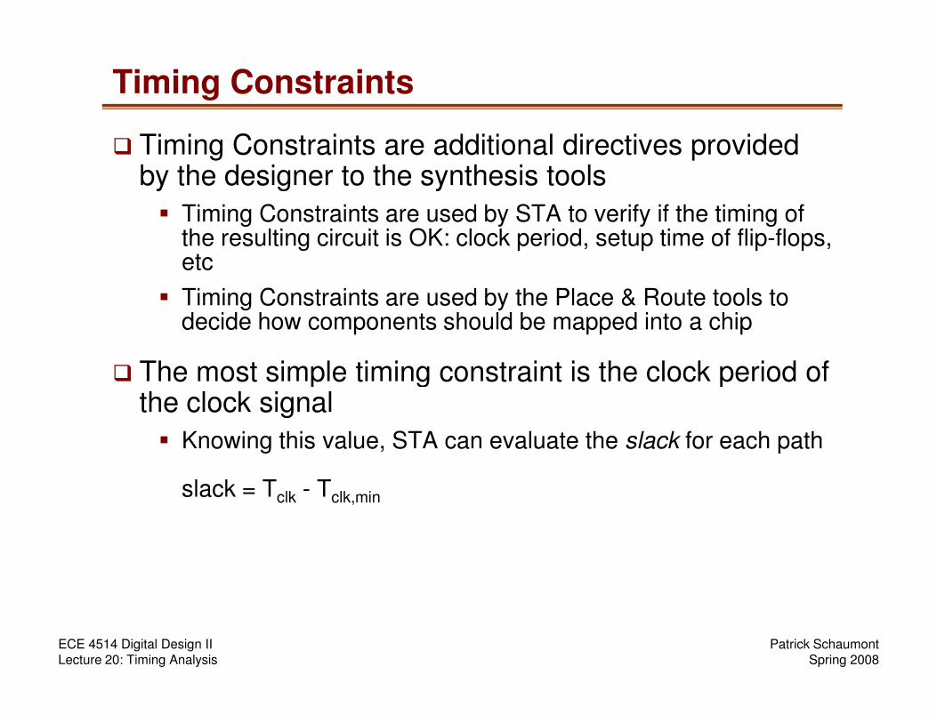
Timing Constraints
� Timing Constraints are additional directives provided by the designer to the synthesis tools
� Timing Constraints are used by STA to verify if the timing of the resulting circuit is OK: clock period, setup time of flip-flops, etc
� Timing Constraints are used by the Place & Route tools to decide how components should be mapped into a chip
� The most simple timing constraint is the clock period of
Patrick SchaumontSpring 2008
ECE 4514 Digital Design IILecture 20: Timing Analysis
� The most simple timing constraint is the clock period of the clock signal
� Knowing this value, STA can evaluate the slack for each path
slack = Tclk - Tclk,min

FPGA Design Flow and Static Timing Analysis
RTL VerilogConstraints
(ucf)
Synthesis(+translate)
- pinout- clock period
No timing information known(apart from cycle boundaries)
Timing estimated based on components only(only fan-out and intrinsic delay)
Patrick SchaumontSpring 2008
ECE 4514 Digital Design IILecture 20: Timing Analysis
Mapper
BitstreamGeneration
Place andRoute
(only fan-out and intrinsic delay)
Timing estimated based on components only(only fan-out and intrinsic delay)
Timing estimated based on finalnetlist (fan-out, intrinsic, and wire delay)
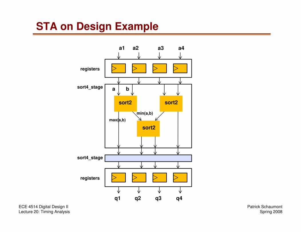
STA on Design Example
sort2 sort2
a b
min(a,b)
a1 a2 a3 a4
sort4_stage
registers
Patrick SchaumontSpring 2008
ECE 4514 Digital Design IILecture 20: Timing Analysis
sort2
max(a,b)
q1 q2 q3 q4
sort4_stage
registers

STA on Design Example
� This design has many equally bad long paths.
� As long as we hit 2 sort2 cells per sorter4_stage, we will be on a long path
� Some examples:
a b
a1 a2 a3 a4
sort4_stage
registers
Patrick SchaumontSpring 2008
ECE 4514 Digital Design IILecture 20: Timing Analysis
sort2 sort2
sort2
max(a,b)
min(a,b)
q1 q2 q3 q4
sort4_stage
registers

STA on Design Example
� We will capture this circuit in Verilog, synthesize it, and evaluate the timing with STA. We need
� sort2
� sort4_stage
� register stage
� top cell
Patrick SchaumontSpring 2008
ECE 4514 Digital Design IILecture 20: Timing Analysis

Sort2 cell
module sorter2c(qa, qb, a, b);
output [3:0] qa, qb;
input [3:0] a, b;
assign qa = (a > b) ? a : b;
assign qb = (a > b) ? b : a;
endmodule
Patrick SchaumontSpring 2008
ECE 4514 Digital Design IILecture 20: Timing Analysis

Sort4_stage
module sort4_stage(q1, q2, q3, q4, a1, a2, a3, a4);
output [3:0] q1, q2, q3, q4;
input [3:0] a1, a2, a3, a4;
wire [3:0] w1, w2, w3, w4;
sorter2 S1 (w1, w2, a1, a2);
sorter2 S2 (w3, w4, a3, a4);
sorter2 S3 (q2, q3, w2, w3);
assign q1 = w1;
Patrick SchaumontSpring 2008
ECE 4514 Digital Design IILecture 20: Timing Analysis
assign q1 = w1;
assign q4 = w4;
endmodulesort2 sort2
sort2
a b
max(a,b)
min(a,b)
a1 a2 a3 a4
sort4_stage

Register stage
module regblock(q1, q2, q3, q4, a1, a2, a3, a4, clk);
output [3:0] q1, q2, q3, q4;
reg [3:0] q1, q2, q3, q4;
input [3:0] a1, a2, a3, a4;
input clk;
always @(posedge clk) begin
q1 <= a1;
q2 <= a2;
q3 <= a3;
Patrick SchaumontSpring 2008
ECE 4514 Digital Design IILecture 20: Timing Analysis
q3 <= a3;
q4 <= a4;
end
endmodule

Toplevel
module fullsorter(q1, q2, q3, q4, a1, a2, a3, a4, clk);
output [3:0] q1, q2, q3, q4;
input [3:0] a1, a2, a3, a4;
input clk;
wire [3:0] w1, w2, w3, w4;
wire [3:0] v1, v2, v3, v4;
wire [3:0] u1, u2, u3, u4;
regblock R0(w1, w2, w3, w4, a1, a2, a3, a4, clk);
Patrick SchaumontSpring 2008
ECE 4514 Digital Design IILecture 20: Timing Analysis
regblock R0(w1, w2, w3, w4, a1, a2, a3, a4, clk);
sort4_stage S0(v1, v2, v3, v4, w1, w2, w3, w4);
sort4_stage S1(u1, u2, u3, u4, v1, v2, v3, v4);
regblock R1(q1, q2, q3, q4, u1, u2, u3, u4, clk);
endmodule

Timing Constraints
� We will only specify the period of the clock signal
� This is done by adding a 'PERIOD' constraint:
NET "clk" PERIOD = 20 ns HIGH 50 %;
NET "clk" TNM_NET = "clk";
Patrick SchaumontSpring 2008
ECE 4514 Digital Design IILecture 20: Timing Analysis
sorter.ucfsorter.v (sort2,
sort4_stage, register stage,
toplevel)
+
Synthesis(+translate)

Synthesis, Translate, Map
� Next, we synthesize the circuit
� After MAP, the Verilog is converted into a netlist of FPGA components: LUTs, flipflops, buffers, etc ..
� You can look at the netlist with the 'Technology Schematic'
� The MAP step can also use static timing analysis on the netlist
� There is a separate interactive timing analysis tool
Patrick SchaumontSpring 2008
ECE 4514 Digital Design IILecture 20: Timing Analysis
� There is a separate interactive timing analysis tool

Timing Analyzer
Delay Summary
Nets +
Patrick SchaumontSpring 2008
ECE 4514 Digital Design IILecture 20: Timing Analysis
Nets + Components
inLongest
Path

Analysis of the 'PERIOD' constraint
============================================================================
Timing constraint: NET "clk_BUFGP/IBUFG" PERIOD = 20 ns HIGH 50%;
30002 items analyzed, 0 timing errors detected. (0 setup errors, 0 hold
errors)
Minimum period is 9.739ns.
---------------------------------------------------------------------------
Slack: 10.261ns (requirement - (data path - clock path skew +
uncertainty))
Source: R0/q4_3 (FF)
Destination: R1/q3_2 (FF)
Requirement: 20.000ns
Patrick SchaumontSpring 2008
ECE 4514 Digital Design IILecture 20: Timing Analysis
Requirement: 20.000ns
Data Path Delay: 9.739ns (Levels of Logic = 12)
Clock Path Skew: 0.000ns
Source Clock: clk_BUFGP rising at 0.000ns
Destination Clock: clk_BUFGP rising at 20.000ns
Clock Uncertainty: 0.000ns
R0/q4_3
R1/q3_2q4, bit 3
a period measures from reg output to reg output
12 levels of logic(includes setup)
9.739 ns

STA on Design Example (after MAP)
sort2 sort2
a b
min(a,b)
a1 a2 a3 a4
sort4_stage
registers R0/q4_3
9.739 ns
Patrick SchaumontSpring 2008
ECE 4514 Digital Design IILecture 20: Timing Analysis
sort2
max(a,b)
q1 q2 q3 q4
sort4_stage
registers R1/q3_2
STA will also tells us what components
are in this path

STA on Design Example (after MAP)
Data Path: R0/q4_3 to R1/q3_2
Delay type Delay(ns) Logical Resource(s)
---------------------------- -------------------
Tiockiq 0.442 R0/q4_3
net (fanout=4) e 0.100 w4<3>
Tilo 0.612 S0/S2/q1_cmp_gt0000121
net (fanout=1) e 0.100 S0/S2/q1_cmp_gt00001_map7
// some lines skipped ...
net (fanout=3) e 0.100 S1/w3<1>
Starting Point
Patrick SchaumontSpring 2008
ECE 4514 Digital Design IILecture 20: Timing Analysis
net (fanout=3) e 0.100 S1/w3<1>
Tilo 0.612 S1/S3/q1_cmp_gt0000145
net (fanout=1) e 0.100 S1/S3/q1_cmp_gt0000145/O
Tilo 0.612 S1/S3/q1_cmp_gt0000173
net (fanout=6) e 0.100 S1/S3/q1_cmp_gt0000
Tilo 0.612 S1/S3/q2<2>1
net (fanout=1) e 0.100 u3<2>
Tioock 0.595 R1/q3_2
---------------------------- ---------------------------
Total 9.739ns (8.439ns logic, 1.300ns route)
(86.7% logic, 13.3% route)
Ending Point

STA on Design Example (after MAP)
Data Path: R0/q4_3 to R1/q3_2
Delay type Delay(ns) Logical Resource(s)
---------------------------- -------------------
Tiockiq 0.442 R0/q4_3
net (fanout=4) e 0.100 w4<3>
Tilo 0.612 S0/S2/q1_cmp_gt0000121
net (fanout=1) e 0.100 S0/S2/q1_cmp_gt00001_map7
// some lines skipped ...
net (fanout=3) e 0.100 S1/w3<1>
LogicDelays(LUTs)
Patrick SchaumontSpring 2008
ECE 4514 Digital Design IILecture 20: Timing Analysis
net (fanout=3) e 0.100 S1/w3<1>
Tilo 0.612 S1/S3/q1_cmp_gt0000145
net (fanout=1) e 0.100 S1/S3/q1_cmp_gt0000145/O
Tilo 0.612 S1/S3/q1_cmp_gt0000173
net (fanout=6) e 0.100 S1/S3/q1_cmp_gt0000
Tilo 0.612 S1/S3/q2<2>1
net (fanout=1) e 0.100 u3<2>
Tioock 0.595 R1/q3_2
---------------------------- ---------------------------
Total 9.739ns (8.439ns logic, 1.300ns route)
(86.7% logic, 13.3% route)

STA on Design Example (after MAP)
Data Path: R0/q4_3 to R1/q3_2
Delay type Delay(ns) Logical Resource(s)
---------------------------- -------------------
Tiockiq 0.442 R0/q4_3
net (fanout=4) e 0.100 w4<3>
Tilo 0.612 S0/S2/q1_cmp_gt0000121
net (fanout=1) e 0.100 S0/S2/q1_cmp_gt00001_map7
// some lines skipped ...
net (fanout=3) e 0.100 S1/w3<1>
NetDelays
(estimated)
Patrick SchaumontSpring 2008
ECE 4514 Digital Design IILecture 20: Timing Analysis
net (fanout=3) e 0.100 S1/w3<1>
Tilo 0.612 S1/S3/q1_cmp_gt0000145
net (fanout=1) e 0.100 S1/S3/q1_cmp_gt0000145/O
Tilo 0.612 S1/S3/q1_cmp_gt0000173
net (fanout=6) e 0.100 S1/S3/q1_cmp_gt0000
Tilo 0.612 S1/S3/q2<2>1
net (fanout=1) e 0.100 u3<2>
Tioock 0.595 R1/q3_2
---------------------------- ---------------------------
Total 9.739ns (8.439ns logic, 1.300ns route)
(86.7% logic, 13.3% route)

STA after Place and Route
� We know the exact loading of each interconnection, so we can get a more precise timing estimate
Patrick SchaumontSpring 2008
ECE 4514 Digital Design IILecture 20: Timing Analysis

Analysis after Place and Route
� We need 10ns more, just to move data around in the chip!
� This is not only the case for this example. In modern logic design, routing delay is typically as large as logic delay !!
========================================================================
Timing constraint: NET "clk_BUFGP/IBUFG" PERIOD = 20 ns HIGH 50%;
30002 items analyzed, 0 timing errors detected. (0 setup errors, 0 hold
Patrick SchaumontSpring 2008
ECE 4514 Digital Design IILecture 20: Timing Analysis
30002 items analyzed, 0 timing errors detected. (0 setup errors, 0 hold
errors)
Minimum period is 19.000ns.
----------------------------------------------------------------------
Slack: 1.000ns (requirement - (data path - clock path
skew + uncertainty))
Source: R0/q1_3 (FF)
Destination: R1/q3_1 (FF)
Requirement: 20.000ns
Data Path Delay: 18.979ns (Levels of Logic = 12)
Clock Path Skew: -0.021ns
Source Clock: clk_BUFGP rising at 0.000ns
Destination Clock: clk_BUFGP rising at 20.000ns
Clock Uncertainty: 0.000ns

Path Analysis confirms that wires are slow ..
Data Path: R0/q1_3 to R1/q3_1
Delay type Delay(ns) Logical Resource(s)
---------------------------- -------------------
Tiockiq 0.442 R0/q1_3
net (fanout=4) 2.142 w1<3>
// some lines skipped ...
Tilo 0.612 S1/S3/q1_cmp_gt0000145
Patrick SchaumontSpring 2008
ECE 4514 Digital Design IILecture 20: Timing Analysis
Tilo 0.612 S1/S3/q1_cmp_gt0000145
net (fanout=1) 0.298 S1/S3/q1_cmp_gt0000145/O
Tilo 0.612 S1/S3/q1_cmp_gt0000173
net (fanout=6) 0.604 S1/S3/q1_cmp_gt0000
Tilo 0.660 S1/S3/q2<1>1
net (fanout=1) 0.725 u3<1>
Tioock 0.595 R1/q3_1
---------------------------- ---------------------------
Total 18.979ns (8.631ns logic, 10.348ns route)
(45.5% logic, 54.5% route)

Summary Static Timing Analysis
� STA uses an analytic delay model based on
� intrinsic gate delay
� fan-out
� wire delay (if available)
� STA will automatically check timing constraints set by a user
Patrick SchaumontSpring 2008
ECE 4514 Digital Design IILecture 20: Timing Analysis
� STA is a good general checking technique but may stumble into false paths
� Analyzing STA results (and improving them) requires an understanding of the netlist by the designer
� but if you want the fastest implementation possible, it may be worth it ..

Dynamic Timing Analysis
� Simulation is used extensively in a digital design flow for verification
� Since this simulation is a timed simulation, we may as well try to use intermediate design representations as simulation targets
� The lower-level synthesis blocks are still pin-compatible with the RTL top-level
Patrick SchaumontSpring 2008
ECE 4514 Digital Design IILecture 20: Timing Analysis
the RTL top-level
� Hence, the same simulation testbench can be used
� Constraint-checking now becomes the role of the designer
� The designer needs to verify if the result of the timed simulation is still corresponding to the results of the RTL simulation
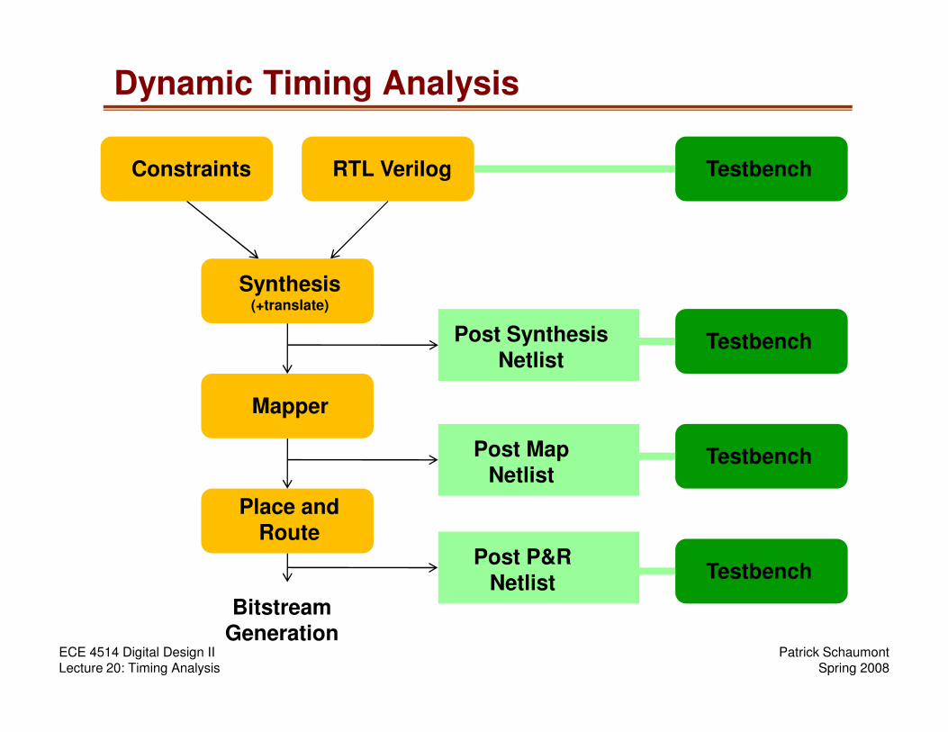
Dynamic Timing Analysis
RTL VerilogConstraints
Synthesis(+translate)
Post SynthesisNetlist
Testbench
Testbench
Patrick SchaumontSpring 2008
ECE 4514 Digital Design IILecture 20: Timing Analysis
Mapper
BitstreamGeneration
Place andRoute
Netlist
Post MapNetlist
Post P&RNetlist
Testbench
Testbench

Dynamic Timing Analysis
RTL Verilog
Post SynthesisNetlist
Netlist in terms of FPGA componentsno logic delay (functional simulation)
requiressimulation
library
Patrick SchaumontSpring 2008
ECE 4514 Digital Design IILecture 20: Timing Analysis
Post MapNetlist
Post P&RNetlist
Netlist in terms of FPGA componentslogic delay included
Netlist in terms of FPGA componentslogic delay and wire delay included

Synthesis and Simulation are integrated
externalsimulator
ISE(synthesis)
Patrick SchaumontSpring 2008
ECE 4514 Digital Design IILecture 20: Timing Analysis

How does a post-synthesis netlist look like?
module sorter2_INST_5 (q1, q2, a1, a2);
output [3 : 0] q1;
output [3 : 0] q2;
input [3 : 0] a1;
input [3 : 0] a2;
// .. some lines skipped
defparam \q1<3>1 .INIT = 4'hE;
LUT2 \q1<3>1 (
.I0(a2[3]),
.I1(a1[3]),
This is a componentfrom an FPGA
simulation library.
The component has anparameter called INIT.
In this case, the parametercaptures the configuration
of a LUT lookup table.
Patrick SchaumontSpring 2008
ECE 4514 Digital Design IILecture 20: Timing Analysis
.I1(a1[3]),
.O(q1[3])
);
// .. some lines skipped
endmodule
The LUT contains an OR.
a2[3] a1[3] q1[3]
0
1
0
1
0
0
1
1
0
1
1
1
= 4'hE

LUT2 from librarymodule LUT2 (O, I0, I1);
parameter INIT = 4'h0;
input I0, I1;
output O;
reg O;
wire [1:0] s;
assign s = {I1, I0};
always @(s)
if ((s[1]^s[0] ==1) || (s[1]^s[0] ==0))
O = INIT[s];
else if ((INIT[0] == INIT[1]) &&
(INIT[2] == INIT[3]) &&
(INIT[0] == INIT[2]))
Patrick SchaumontSpring 2008
ECE 4514 Digital Design IILecture 20: Timing Analysis
(INIT[0] == INIT[2]))
O = INIT[0];
else if ((s[1] == 0) && (INIT[0] == INIT[1]))
O = INIT[0];
else if ((s[1] == 1) && (INIT[2] == INIT[3]))
O = INIT[2];
else if ((s[0] == 0) && (INIT[0] == INIT[2]))
O = INIT[0];
else if ((s[0] == 1) && (INIT[1] == INIT[3]))
O = INIT[1];
else
O = 1'bx;
endmodule

How does a post-PAR netlist look like?
� Contains placement information and uses library components that support timing specifications
module sorter2_INST_5 (a1, a2, q1, q2);
input [3 : 0] a1;
input [3 : 0] a2;
output [3 : 0] q1;
output [3 : 0] q2;
// some lines skipped ..
LUT configuration
Patrick SchaumontSpring 2008
ECE 4514 Digital Design IILecture 20: Timing Analysis
// some lines skipped ..
defparam q1_cmp_gt0000143.INIT = 16'h22B2;
defparam q1_cmp_gt0000143.LOC = "SLICE_X25Y91";
X_LUT4 q1_cmp_gt0000143 (
.ADR0(a1[1]),
.ADR1(a2[1]),
.ADR2(a1[0]),
.ADR3(a2[0]),
.O(\q1_cmp_gt0000143/O )
);
Placementinformation

SDF Timing Information
� Timing information from Place and Route is not stored in the Post-PAR netlist, but in a separate SDF File (Standard Delay Format)
� The Modelsim simulator will read this SDF file together with the Verilog netlist and back-annotate the delay information from the SDF file into the netlist
Patrick SchaumontSpring 2008
ECE 4514 Digital Design IILecture 20: Timing Analysis
Verilog Netlist
Place and Route
SDF Data
ModelsimPost-PAR
Simulation
Testbench
Verilog Netlist with Placement Information

Demonstration
� (this slide shows the demo script. I will upload the sorter example on Blackboard)
� Include testbench with sorter design
� Choices for Post-nnnnn models:
� Post-synthesis, Post-translate, Post-map, Post-PAR model
� Post-PAR Static Timing Analysis
Patrick SchaumontSpring 2008
ECE 4514 Digital Design IILecture 20: Timing Analysis
� Post-PAR Static Timing Analysis
� Analyze -> against timing constraints
� Slowest path: R0/q4 to R1/q3
� (if time left: cross-probe feature)
Demonstration (2)
� Simulate Post-PAR Model
� Ilustrate delay & cross check with STA
� Show netlist
� Post-synthesis
� Isolate one component (LUT)
� Verify LUT location in simulation library
Patrick SchaumontSpring 2008
ECE 4514 Digital Design IILecture 20: Timing Analysis
� Post-PAR
� Compare Post-PAR component with post-synthesis

Summary STA and Timed Simulation
� Static Timing Analysis estimates the worst possible delay in a network based on network topology and components
� Dynamic Timing Analysis performs a timed simulation, with time delays modeled based on the intermediate synthesis results
Patrick SchaumontSpring 2008
ECE 4514 Digital Design IILecture 20: Timing Analysis
� Performance optimizations will typically use static timing analysis. Specific worst-case conditions can be easily triggered using dynamic timing analysis.
Top Related