


Languages
Pages
Legal


Design Techniques for 45nm SOI Technology
Christophe FreyEngineering manager – SOI design center
22
AgendaSOI introductionSOI design ChallengesStandard cell designIO designHistory effect characterizationMemory design

33
SOI: Silicon On InsulatorRefers to the use of an SOI waferVariable thickness
Top silicon film Thick film > 300nmThin film < 300nm
Buried oxide < 1µmElectrical behavior of SOI transistors related to top silicon thickness
Thick film: similar to bulk CMOS (body not floating)Thin film: partially depleted or fully-depleted (body floating)
SOI introduction

44
Performance benefits of SOI cmosSpeed
Reduced junction area & capacitanceThreshold voltage (Vt) dyn lowering
More current at same VddSame speed at lower Vdd, lower power
AreaDenser circuit layout
No well tiesReduced transistor spacing
Higher SOI transistor drive currentSynthesis tool will pick smaller cell in SOI for a given C load
STI
VddVss PMOSNMOS
N+ N+ P+ P+
P substrate
Buried oxide
SOI CMOS inverter
Vss
STI N well
P+ N+
PMOSNMOS
N+ N+ P+ P+
P substrate
Vdd
Bulk CMOS inverter
STI
VddVss PMOSNMOS
N+ N+ P+ P+
P substrate
Buried oxide
SOI CMOS inverter
Vss
STI N well
P+ N+
PMOSNMOS
N+ N+ P+ P+
P substrate
Vdd
Bulk CMOS inverter
Floating body
55
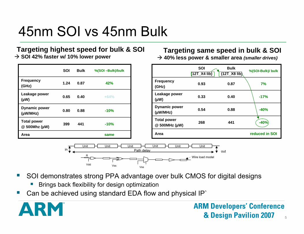
reduced in SOIArea
7%0.870.93Frequency(GHz)
-40%441268Total power @ 500MHz (µW)
-40%0.880.54Dynamic power(µW/MHz)
-17%0.400.33Leakage power(µW)
%(SOI-Bulk)/ bulkBulk
(12T_X8 lib)SOI
(12T_X4 lib)
45nm SOI vs 45nm Bulk
SOI demonstrates strong PPA advantage over bulk CMOS for digital designsBrings back flexibility for design optimization
Can be achieved using standard EDA flow and physical IP`
Targeting highest speed for bulk & SOISOI 42% faster w/ 10% lower power
Targeting same speed in bulk & SOI40% less power & smaller area (smaller drives)
sameArea
441
0.88
0.40
0.87
Bulk
42%1.24Frequency(GHz)
-10%399Total power@ 500Mhz (µW)
-10%0.80Dynamic power(µW/MHz)
+64%0.65Leakage power(µW)
%(SOI –Bulk)/bulkSOI
outUnit Unit Unit UnitUnit Unit
Path delayR
Vdd Vss Vss
in
Wire load model

SOI design challenges
Standard cell designIO designHistory effect characterization
77
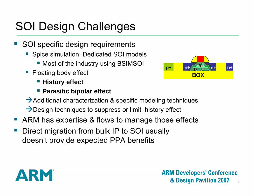
SOI Design ChallengesSOI specific design requirements
Spice simulation: Dedicated SOI modelsMost of the industry using BSIMSOI
Floating body effect History effectParasitic bipolar effect
Additional characterization & specific modeling techniquesDesign techniques to suppress or limit history effect
ARM has expertise & flows to manage those effectsDirect migration from bulk IP to SOI usually doesn’t provide expected PPA benefits
BOXp+ n+ n+ n+p fb

88
Parasitic bipolar effect in an SOI transistor
Body is the base of the parasitic bipolarVbs=Vbe determines the amount of bipolar current
Body is floating and D/S variations couple to the bodyBody dynamic behaviour is important
D/S can couple charges to the floating bodyVt of the transistor is changed (good for speed)But D can couple to S through floating body
Substrate
Source
Gate
DrainVbs
Vbg
Vbox
Vbd
Body
Base=Body
E C
DS
G

99
Standard cellsDesign sensitivity to SOI
Some SOI specific effects may impact functionalitySequential cells architecture must be carefully selected to avoid functional failure
Timing sensitivity to SOIFloating body effects are state and transition dependentStandard cells are used for random logic, thus history effects are unavoidableCareful timing characterization is necessary

1010
Standard cell functional failure example
D
S
S
D=vdd
CKBI=0
vbn=
vdd
D=vdd?CKBI=0
S=0 Ibipolar
Ibipolar: with floating body
0.15u SOI technology example
D
Body tied to gnd
Body tied to gnd
No fail
Floating body
failBase=Body
E C
VBE=0.8V
0.15µm technologyLatch with passgate is not safe!
S=1
body
vbe
1111
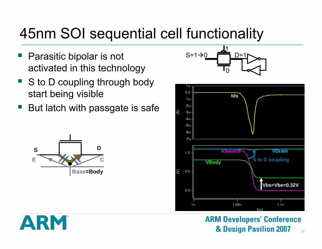
45nm SOI sequential cell functionalityParasitic bipolar is not activated in this technologyS to D coupling through body start being visibleBut latch with passgate is safe
VDrain
VBody
VSource
Ids
D=1S=1 0
0
1
Vbs=Vbe=0.32V
Base=Body
E C
DSS to D coupling
1212
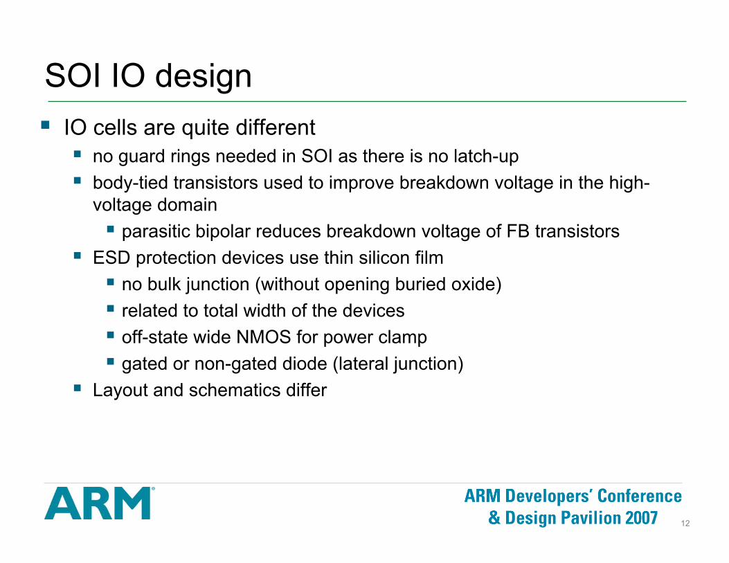
SOI IO designIO cells are quite different
no guard rings needed in SOI as there is no latch-upbody-tied transistors used to improve breakdown voltage in the high-voltage domain
parasitic bipolar reduces breakdown voltage of FB transistorsESD protection devices use thin silicon film
no bulk junction (without opening buried oxide)related to total width of the devicesoff-state wide NMOS for power clampgated or non-gated diode (lateral junction)
Layout and schematics differ

1313
SOI IO designESD protection: RC-triggered power clamp
uses body-tied transistorFB transistor may be used in low-voltage domain
leakage current reduced
Voltage tolerant IO (i.e voltage > maximum tolerated for the transistor (e.g. 3.3V/2.5V))
SOI dielectric isolation greatly facilitates the implementation
BULK requires isolated well (triple-well process) if drain-body junction breakdown voltage < high voltage (3.6V WC)
No body effect (vbs=0) smaller nmos
VDD
VSS
Powerclamp
R
C
2.5
0
0
3.3
2.5
0
2.5-Vt

1414
History effect timing characterizationBody potential depends on the history of the devices.We commonly define two dc states:
DC0: input is low (0V)DC1: input is high (Vdd)
1 10 100 1000 10000 1000007.50E-12
8.00E-12
8.50E-12
9.00E-12
9.50E-12
1.00E-11
1.05E-11
1.10E-11
1.15E-11
1.20E-11
1.25E-11
num ber of cycles
inve
rter
del
ay (
s)
Tphl_dc0
Tphl_dc1
Tplh_dc1
Tplh_dc0
T (DC)= 0
UT (DC)= 1
First transitions show largest variations
steady state
1515
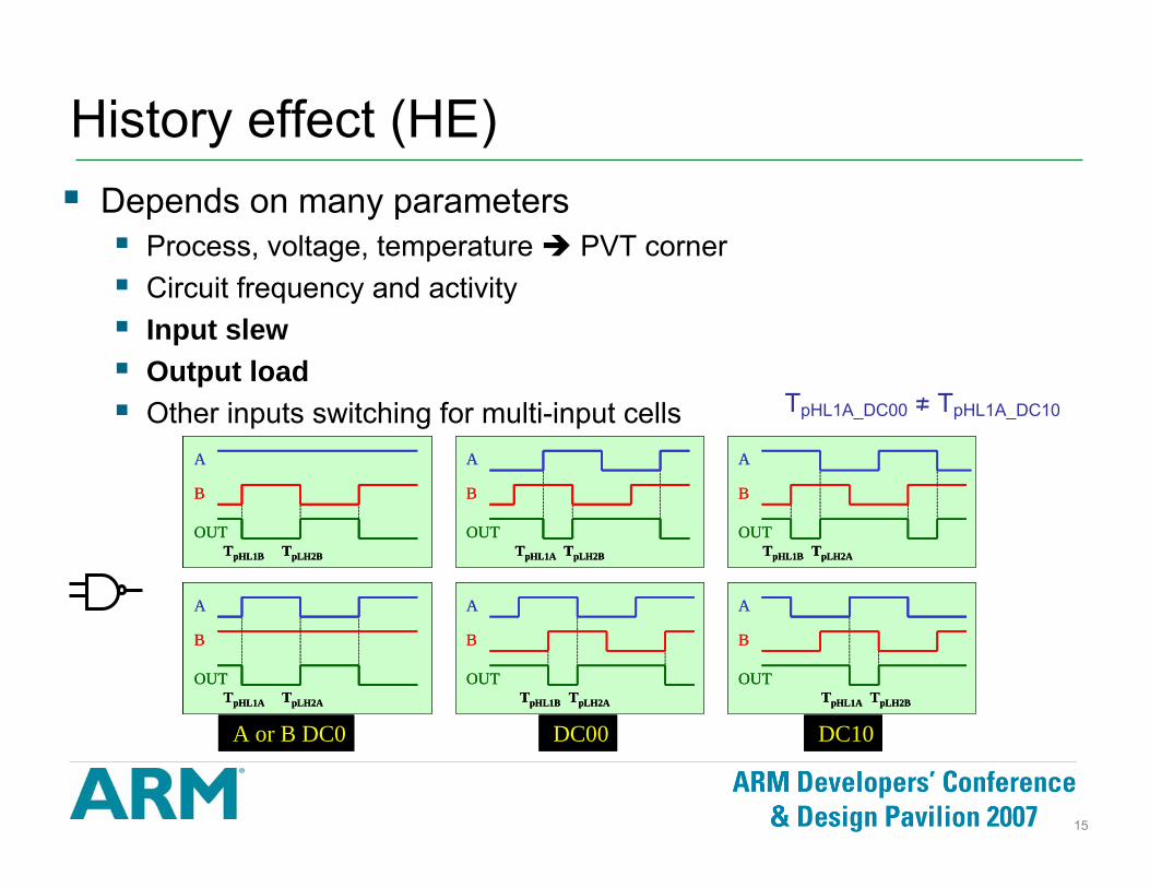
History effect (HE)Depends on many parameters
Process, voltage, temperature PVT cornerCircuit frequency and activityInput slewOutput loadOther inputs switching for multi-input cells
A
B
OUTTpHL1B TpLH2B
A
B
OUTTpHL1B TpLH2B
A
B
OUTTpHL1B TpLH2B
A
B
OUTTpHL1A TpLH2A
A
B
OUTTpHL1A TpLH2A
A
B
OUTTpHL1A TpLH2A
A
B
OUTTpHL1A TpLH2B
A
B
OUTTpHL1A TpLH2B
A
B
OUTTpHL1A TpLH2B
A
B
OUTTpHL1B TpLH2A
A
B
OUTTpHL1B TpLH2A
A
B
OUTTpHL1B TpLH2A
A
B
OUTTpHL1B TpLH2A
A
B
OUTTpHL1B TpLH2A
A
B
OUTTpHL1B TpLH2A
A
B
OUTTpHL1A TpLH2B
A
B
OUTTpHL1A TpLH2B
A
B
OUTTpHL1A TpLH2B
DC00 DC10A or B DC0
A
B
OUTTpHL1B TpLH2B
A
B
OUTTpHL1B TpLH2B
A
B
OUTTpHL1B TpLH2B
A
B
OUTTpHL1A TpLH2A
A
B
OUTTpHL1A TpLH2A
A
B
OUTTpHL1A TpLH2A
A
B
OUTTpHL1A TpLH2B
A
B
OUTTpHL1A TpLH2B
A
B
OUTTpHL1A TpLH2B
A
B
OUTTpHL1B TpLH2A
A
B
OUTTpHL1B TpLH2A
A
B
OUTTpHL1B TpLH2A
A
B
OUTTpHL1B TpLH2A
A
B
OUTTpHL1B TpLH2A
A
B
OUTTpHL1B TpLH2A
A
B
OUTTpHL1A TpLH2B
A
B
OUTTpHL1A TpLH2B
A
B
OUTTpHL1A TpLH2B
A
B
OUTTpHL1B TpLH2B
A
B
OUTTpHL1B TpLH2B
A
B
OUTTpHL1B TpLH2B
A
B
OUTTpHL1A TpLH2A
A
B
OUTTpHL1A TpLH2A
A
B
OUTTpHL1A TpLH2A
A
B
OUTTpHL1A TpLH2B
A
B
OUTTpHL1A TpLH2B
A
B
OUTTpHL1A TpLH2B
A
B
OUTTpHL1B TpLH2A
A
B
OUTTpHL1B TpLH2A
A
B
OUTTpHL1B TpLH2A
A
B
OUTTpHL1B TpLH2A
A
B
OUTTpHL1B TpLH2A
A
B
OUTTpHL1B TpLH2A
A
B
OUTTpHL1A TpLH2B
A
B
OUTTpHL1A TpLH2B
A
B
OUTTpHL1A TpLH2B
DC00 DC10A or B DC0
TpHL1A_DC00 ≠ TpHL1A_DC10
1616
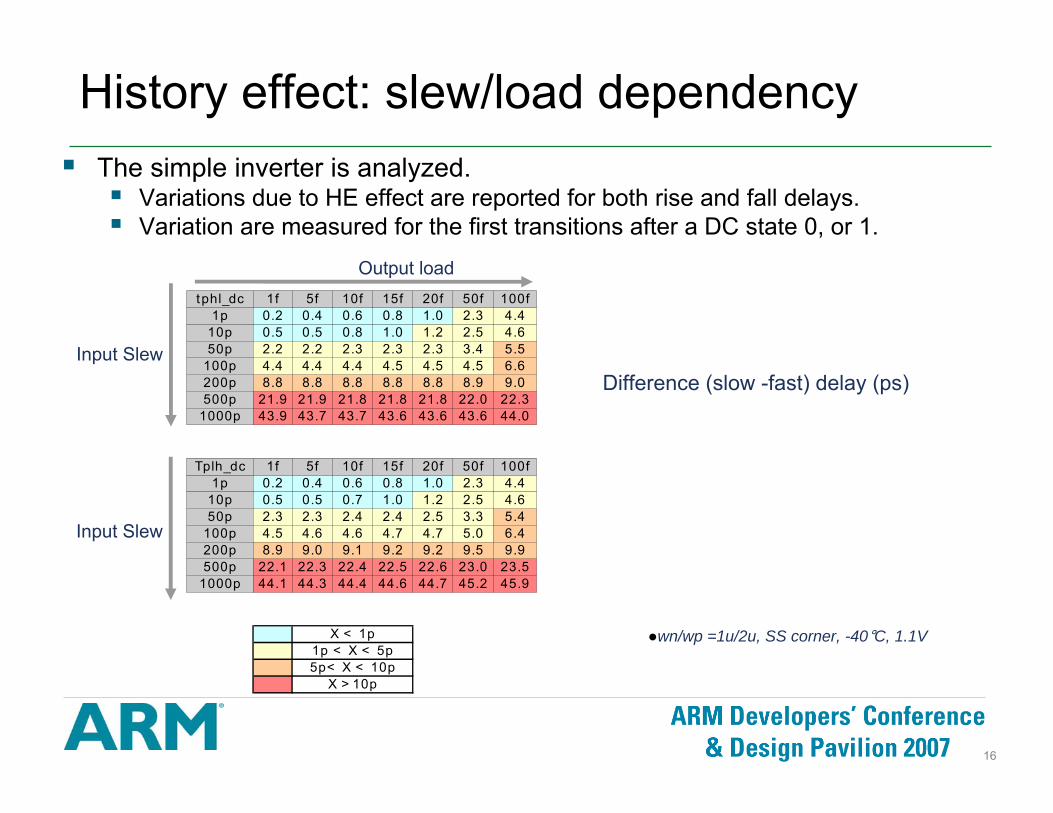
History effect: slew/load dependency
Output load
Input SlewDifference (slow -fast) delay (ps)
●wn/wp =1u/2u, SS corner, -40°C, 1.1V
Input Slew
tphl_dc 1f 5f 10f 15f 20f 50f 100f1p 0.2 0.4 0.6 0.8 1.0 2.3 4.4
10p 0.5 0.5 0.8 1.0 1.2 2.5 4.650p 2.2 2.2 2.3 2.3 2.3 3.4 5.5
100p 4.4 4.4 4.4 4.5 4.5 4.5 6.6200p 8.8 8.8 8.8 8.8 8.8 8.9 9.0500p 21.9 21.9 21.8 21.8 21.8 22.0 22.3
1000p 43.9 43.7 43.7 43.6 43.6 43.6 44.0
Tplh_dc 1f 5f 10f 15f 20f 50f 100f1p 0.2 0.4 0.6 0.8 1.0 2.3 4.4
10p 0.5 0.5 0.7 1.0 1.2 2.5 4.650p 2.3 2.3 2.4 2.4 2.5 3.3 5.4
100p 4.5 4.6 4.6 4.7 4.7 5.0 6.4200p 8.9 9.0 9.1 9.2 9.2 9.5 9.9500p 22.1 22.3 22.4 22.5 22.6 23.0 23.5
1000p 44.1 44.3 44.4 44.6 44.7 45.2 45.9
X < 1p1p < X < 5p5p< X < 10p
X > 10p
The simple inverter is analyzed. Variations due to HE effect are reported for both rise and fall delays. Variation are measured for the first transitions after a DC state 0, or 1.

1717
History effect characterizationHE is very complex and cannot be characterized exhaustively
Need to simplify and keep compatibility with timing analysis tools
Use 1st/2nd switch characterization when steady-state is within reasonable range current ARM characterization
HE analysis is performed before characterizationSteady-state characterization if needed requires fast algorithm to keepcontrol of production characterization time
Create two SOI corners for every PVT cornerminsoi: minimum delay and slewmaxsoi: maximum delay and slew
Ideally these corners should be mixed with local variationsUse EDA tools capability of handling local variations

1818
HE in design flow
clk
clk
SETUP
HOLD
use MAXSOI library
use MINSOI library
use MINSOI library
D
D
CK
CKlatest arriving signal at D must arrive before the earliest arriving signal at CK
earliest arriving signal at D must arrive after the latest arriving signal at CK
use MAXSOI library
We are providing min/max SOI cornersinstruct STA to use the min/max SOI data for -min/max OCV analysisallowing for Clock Reconvergence Pessimism Removal
launch clk
capture clk
SOI Memory design
SOI effects regarding the memory biitcellBipolar current during Write OperationImpact of History Effect (HE) on read currentDynamic read current versus DC read current
SOI effects regarding the Sense Amplifier (S/A)S/A mismatch (offset) induced by HE with FB devicesUse of specific SOI devices (BC MOS)HE on S/A delay (w/wo Body tied devices)
SOI effects regarding Setup, hold times, Signals races

2020
Bipolar current & Write operationAssuming the column of bitcells is initialized to 1.
the body of pass-gates are set to a value close to 1
When writting 0 in 1 bitcellBitline is fallingThe body of all unselected cells is coupled lowBut slower than the bitline
A positive Vbe is observed
All unselected cell have a parasitic bipolar currentIs it big enough to harm write functionality?Has the write driver been sized accordingly
1
1
1
1
1
WL=1
BLBLI
1
0 Base=body
CE
0
0
0
0

2121
Example parasitic bipolar study
1 1 00.77->0.32
0
D
SOURCE
DRAIN
VBS
VBD
Vbody
Vbe=Vbs increases up to 0.32VThis is low enough to keep negligible the parasitic bipolar current
This needs to be checkedFor every technologyIn worst case conditions
S

2222
SOI effects on read currentSRAM margin analysis (read current and signal generation)
Is traditionally based on a constant Iread (determined by DC simulation)Plus a deviation due to local variations determined independently
In SOI though Iread will depend on the state of the body.DC analysis assumes the body has stabilizedActually the transient behavior of the body changes the value of Iread
before WL is rising the body is lower on PG (no charge through gate & source)But the body is raised when WL rises through couplingIt is not obvious if the body is lower or higher than in the DC caseDepending on the body voltage Iread may by more or less than in DC
In addition an history effect can be observed on read currentDepending on activity
2323
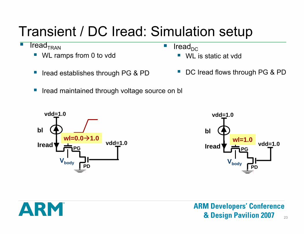
Transient / DC Iread: Simulation setupIreadDC
WL is static at vdd
DC Iread flows through PG & PD
PG
PD
blwl=1.0
vdd=1.0
vdd=1.0
Vbody
Iread
IreadTRANWL ramps from 0 to vdd
Iread establishes through PG & PD
Iread maintained through voltage source on bl
PG
PD
bl
vdd=1.0
vdd=1.0
Vbody
Ireadwl=0.0 1.0

2424
TRAN / DC Iread: resultsCompared to DC, TRANVbody VTPG Iread
-1.5%
71.3
0.65
TRAN
72.4
0.72
DC
Iread (µA)∆Iread
Vibody
65nm GP cell
Typical corner65nm BSIMSOI3.2 SRAM spice models
Vbody is coupled high by wl
Vbody
Iread
Iread
Vbody
WL
DC
TRAN
19.116.8Iread (µA)
+13.7%∆Iread
TRANDC45nm LP cell Vbody VTPG Iread
IreadTRAN can be more or less than IreadDCDepending on the transistor optimization and technolgy node
IreadTRAN needs to be carefully characterized Then only the traditional Iread statistical margin analysis can start

2525
Activity dependency of Read operation
HE depends on previous state, body voltages can be different Thus modifying read current
Considering 2 Read0 cycles, with DC0 & DC1 on node IT:DC0-R0 (1st switch)DC1-W0-R0 (2nd switch)
Vbpg & Vbpd will be differentAs a consequence Iread will be different
4841Iread (uA)+-VBpd (V)+-VBpg (V)
IT DC1/W0/R0IT DC0/R0
Bpg
Bp
Bpd
Bpb
Bpdb_
Bpgb0 1
BT BB
Iread
ITIB
40.0
41.0
42.0
43.0
44.0
45.0
46.0
47.0
48.0
49.0
1 10 100 1000 10000 100000
17%
DC1
DC0
Iread
cycles
2626
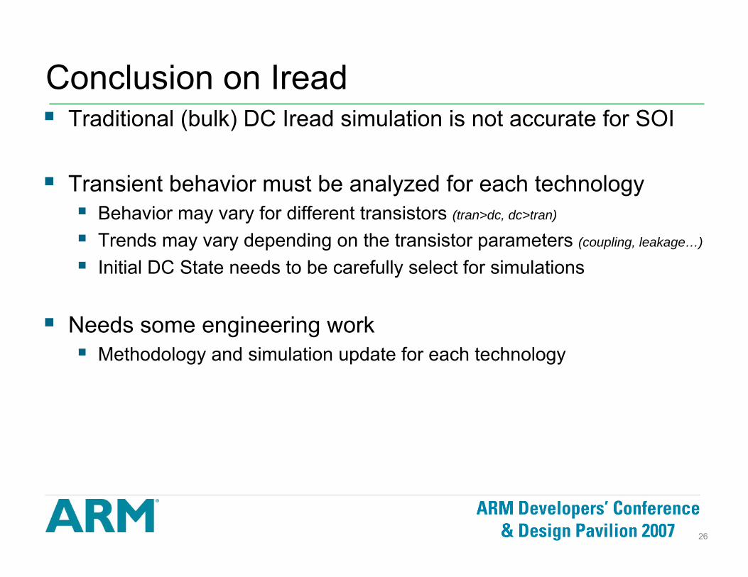
Conclusion on IreadTraditional (bulk) DC Iread simulation is not accurate for SOI
Transient behavior must be analyzed for each technologyBehavior may vary for different transistors (tran>dc, dc>tran)
Trends may vary depending on the transistor parameters (coupling, leakage…)
Initial DC State needs to be carefully select for simulations
Needs some engineering workMethodology and simulation update for each technology

2727
Sense Amp Dynamic Effects
01
BNTvbvtt
BNBvbvtb
Q
VDD
SAEN
SAE
QB
For repeated read cycle in the same state, a body voltage differential develops between BNB & BNT, BPB & BPT.
Example above: read 0, implies VBNB rising while VBNT decreasing. The body voltage difference can be reduced with body contacted transistors
0 20000 40000 600000.88
0.90
0.93
0.95
0.98
1.00
1.03
1.05
1.08
1.10
1.13
1.15
1.18
num ber of cycles
Bod
y vo
ltag
e (V
)
VBNT
VBNB
VBPT
VBPB
BPB BPT
Leads to 15mV offset (typical corner)

2828
Sense Amp alternative body connections
1 10 100 1000 10000 1000002.10E-112.15E-112.20E-112.25E-112.30E-112.35E-112.40E-112.45E-112.50E-112.55E-112.60E-112.65E-112.70E-112.75E-112.80E-112.85E-112.90E-112.95E-11
number of cycles
SAE
to Q
del
ay (
s)
SA2
SA1
SA3
QT
VDD
SAEN
SAE
RB
QB
RT
GND
QT
VDD
SAEN
SAE
RB
QB
RT
QT
VDD
SAEN
SAE
RB
QB
RT
SA1 SA2 SA3
Fully floating body (SA3) is not selected for SOI technologyThe speed gain is wasted into extra margin required for functionality
Body contacted transistors are usedStill at high frequency, and repeated ‘read1' or ‘read0' a difference between the two matched transistors can develop.The subsequent systematic offset needs to be limited by design
1 10 100 1000 10000 1000000.0
0.5
1.0
1.5
2.0
2.5
3.0
3.5
4.0
4.5
number of cycles%
of S
AE t
o Q
del
ay v
aria
tion
due
SA2
SA1
SA3
2929
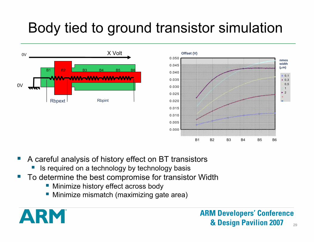
Body tied to ground transistor simulation
Rbpext Rbpint
0V
0V X Volt
0.000
0.005
0.010
0.015
0.020
0.025
0.030
0.035
0.040
0.045
0.050
0,10,30,512
Offset (V)
nmoswidth (µm)
A careful analysis of history effect on BT transistorsIs required on a technology by technology basis
To determine the best compromise for transistor WidthMinimize history effect across bodyMinimize mismatch (maximizing gate area)
B1 B2 B3 B4 B5 B6
B1 B2 B3 B4 B5 B6

3030
History effect in SRAM self timed loops
Bulk style design CK ICK_RC RESET
Slew Rate (ps) 500 160 65
(DC0 -DC1) TPD difference (ps) 0 32.7 48.2
(DC0 -DC1) TPD variation (%) 0 65 50
CK
ICK_RC
DWL
RESET
Pulse generator
65%
~50%
A 500ps input slope is applied on CK pinWC corner for History effect (SS, -40°C, 1.1V)
GTP
RESET
ImprovedPulse
generator
1.4% ~1%
Final optimization CK ICK_RC RESET
Slew Rate (ps) 500 65 65
(DC0 -DC1) TPD difference (ps) 0 0.7 1
(DC0 -DC1) TPD variation (%) 0 1.38 1
CK
Proper design style leads to drastic reduction of history effect (50ps 1ps)
3131
ConclusionA variety of SOI effects must be studied and quantified
AC behavior, History effect & DC state, parasitic bipolar, body behavior…Can not be neglected to check functionalityAre to large to simply include in margin
SOI dedicated engineering is keyMagnitude of effects are technology dependentSOI effects can be limited by good design practice
SOI benefits can be lost by design (e.g simple SOI/Bulk porting)ARM has the SOI IP design know-how and flows in place
Physical IP design style adapted for each projectExperienced SOI designers
IP development infrastructure is adapted for SOISOI challenges are transparent to the IP end users
standard EDA flow can be usedIP logic functionality and interface identical to bulk
Top Related