


Languages
Pages
Legal


Design Rules,
Technology File, DRC / LVS
Prof. Dr. Peter Fischer
VLSI Design: Design Rules P. Fischer, TI, Uni Mannheim, Seite 1

DESIGN RULES

Rules in one Layer
§ Caused by manufacturing limits (lithography, etching,..) § Rules: Spacing, Width, Notch (='Kerbe') between same net
• Finest structure is Poly-silicon for gates
§ Some structures have ‘=‘ rules, i.e. must have exactly a fixed size. Prominent example: contacts and vias
§ Larger structures must be created by repetition (‘mosaic’):
VLSI Design: Design Rules P. Fischer, ziti, Uni Heidelberg, Seite 3
spacing width notch Not allowed!

Rules in one Layer: Wide Structures
§ Spacing rules often apply for ‘large’ = wide structures § For instance
• gate spacing for gates > Lmin is different (larger) • Metal spacing for metal wider Wmin can be different • Via overlap can be more for wide metal
§ How to find wide metal? • Can use ‘geomSize’ function which expands / shrinks shape
• Shapes <6 units disappear (after shrink / expand)
VLSI Design: Design Rules P. Fischer, ziti, Uni Heidelberg, Seite 4
Size -3 Size +3
Size -3 Size +3

Rules in one Layer: Slots
§ There are also Maximum rules: • Manufacturing of large continuous regions can lead to stress /
cracks • Definition of size limitation (for instance):
‘no square of 10×10µm2 may fit on the metal’
§ ‘wide metal’ must be ‘slotted’ (holes) • This can be by chopping out metal or • By adding shapes on a ‘metal-slot’ layer. These can be copied!
Objects on that layer will later be subtracted.
• Slots should not cut current flow →
VLSI Design: Design Rules P. Fischer, ziti, Uni Heidelberg, Seite 5
Test rectangle
slots

Rules between Layers
§ Caused by alignment precision of different masks
§ Extension of gate:
§ Enclosure / Overlap • ‘NWELL enclosure of pplus’:
VLSI Design: Design Rules P. Fischer, ziti, Uni Heidelberg, Seite 6
Drain
Source
Gate
Shifted poly layer
Fatal: Short between drain and source
extension
enclosure NWELL
pplus

Overlap Required on Drain/Source-Diodes
§ Consider contacts of Drain / Source (NMOS)
§ Solution: Contact hole must be smaller than 'active‘:
VLSI Design: Design Rules P. Fischer, ziti, Uni Heidelberg, Seite 7
n+
Alu
SiO2
p-
Ideal (minimal n+ size)
Misaligned contact mask:
n+
Short circuit between drain/source and substrate p-
n+
p-
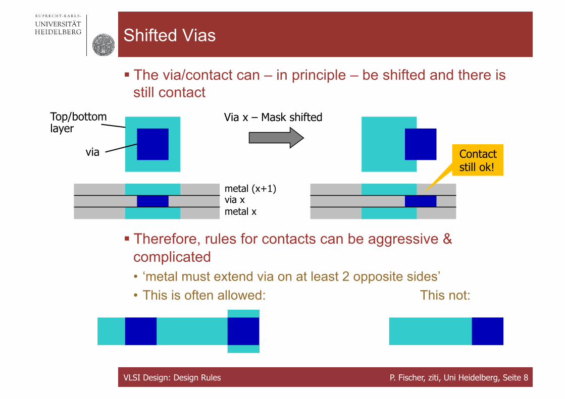
Shifted Vias
§ The via/contact can – in principle – be shifted and there is still contact
§ Therefore, rules for contacts can be aggressive &
complicated • ‘metal must extend via on at least 2 opposite sides’ • This is often allowed: This not:
VLSI Design: Design Rules P. Fischer, ziti, Uni Heidelberg, Seite 8
Top/bottom layer
Via x – Mask shifted
metal (x+1) via x metal x
via Contact still ok!
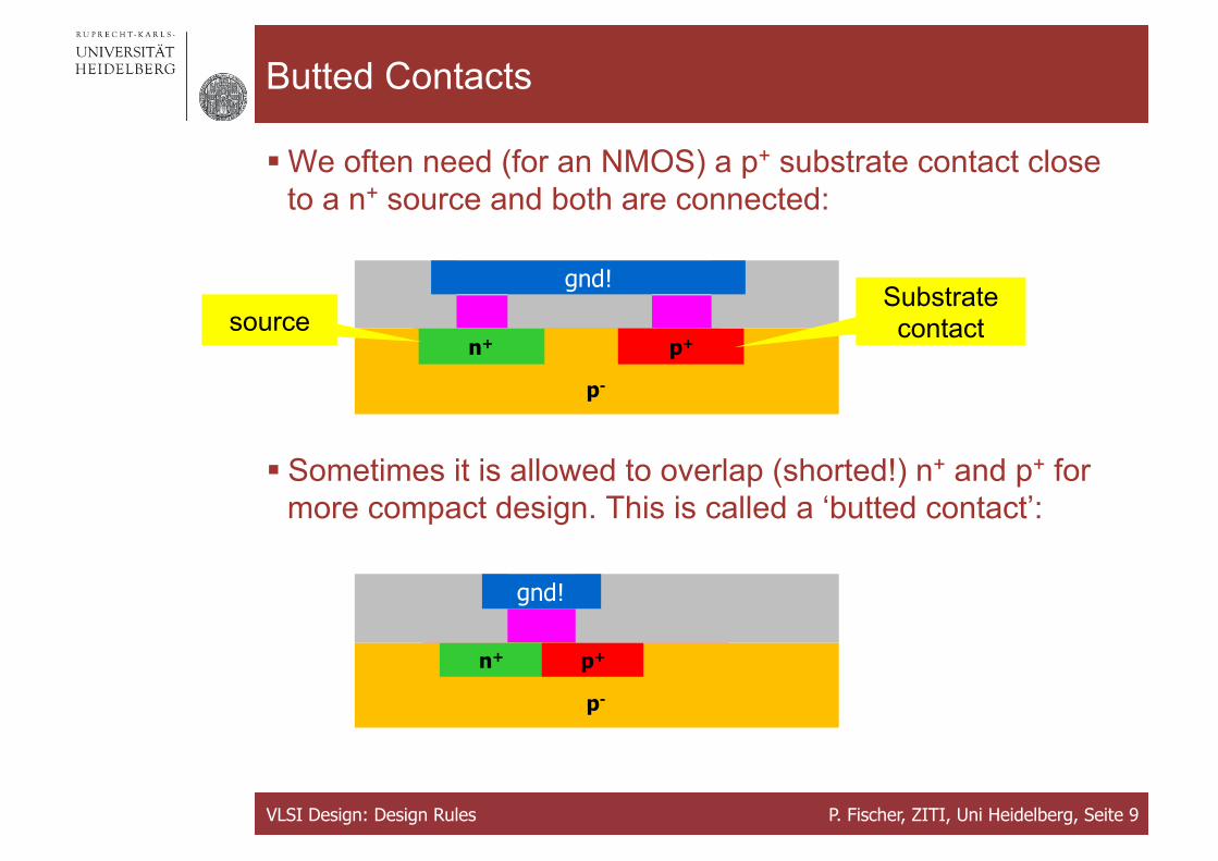
Butted Contacts
§ We often need (for an NMOS) a p+ substrate contact close to a n+ source and both are connected:
§ Sometimes it is allowed to overlap (shorted!) n+ and p+ for more compact design. This is called a ‘butted contact’:
VLSI Design: Design Rules P. Fischer, ZITI, Uni Heidelberg, Seite 9
n+
p-
p+
gnd!
source Substrate contact
n+
p-
p+
gnd!
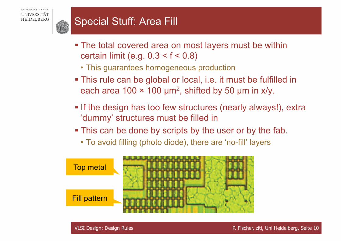
Special Stuff: Area Fill
§ The total covered area on most layers must be within certain limit (e.g. 0.3 < f < 0.8) • This guarantees homogeneous production
§ This rule can be global or local, i.e. it must be fulfilled in each area 100 × 100 µm2, shifted by 50 µm in x/y.
§ If the design has too few structures (nearly always!), extra ‘dummy’ structures must be filled in
§ This can be done by scripts by the user or by the fab. • To avoid filling (photo diode), there are ‘no-fill’ layers
VLSI Design: Design Rules P. Fischer, ziti, Uni Heidelberg, Seite 10
Fill pattern
Top metal

Special Stuff: Antenna
§ Some process steps can deposit static charge on structures • Amount of charge can depend on area or on periphery
§ The charge Q leads to a voltage U = Q/C which can destroy transistor gates • Most dangerous for large structure (large Q) and small gate
(small C) § The ratio is calculated for each gate. If it exceeds a value,
there is danger for an antenna error. § Antenna errors are eliminated if
• A drain of a MOS is connected directly. The drain diode has enough leakage to discharge the gate. Often, the ‘driver’ is connected through higher metals and is not ‘seen’ in the early process steps
• An explicit ‘tie-down’ diode is added (n+ in p-substrate) • Signals are fed through higher metals, so that the driving gate is
seen when the metal connects (see next page)
VLSI Design: Design Rules P. Fischer, ziti, Uni Heidelberg, Seite 11

Special Stuff: Antenna (example for NMOS)
VLSI Design: Design Rules P. Fischer, ZITI, Uni Heidelberg, Seite 12
p-
antenna gate
n+ OK
BAD p-
antenna Protection by driver
antenna metal2 comes later
p- tie down OK
n+
p-
OK bridge to upper layers reduces antenna size at gate end
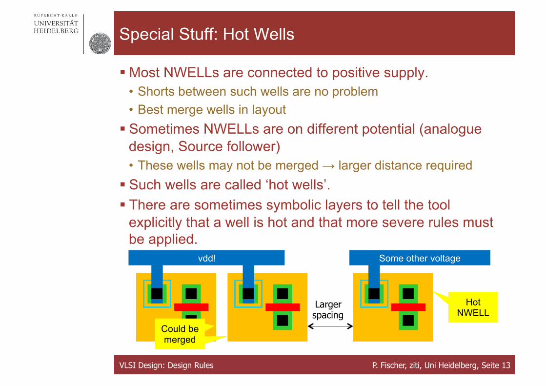
Special Stuff: Hot Wells
§ Most NWELLs are connected to positive supply. • Shorts between such wells are no problem • Best merge wells in layout
§ Sometimes NWELLs are on different potential (analogue design, Source follower) • These wells may not be merged → larger distance required
§ Such wells are called ‘hot wells’. § There are sometimes symbolic layers to tell the tool
explicitly that a well is hot and that more severe rules must be applied.
VLSI Design: Design Rules P. Fischer, ziti, Uni Heidelberg, Seite 13
Larger spacing
vdd! Some other voltage
Hot NWELL
Could be merged
Could be merged

ERC = 'Electrical Rule Check'
§ ERC Examples: • Floating Metal, Poly,... • Antenna rules • Shorted Drain & Source of a MOS • No substrate- or well contact ('figure having no stamped
connection') • Different contacts of substrate / well are connected to different
nets ('Figure having multiple stamped connections') (No automatic connection of these nets to avoid circuit parts which are only connected via substrate – can be fatal!)
• Distance of MOS to next substrate / well contact too large (Latchup rule)
§ Difference between DRC und ERC is soft • DRC must sometimes ‚understand‘ the circuit
VLSI Design: Design Rules P. Fischer, ziti, Uni Heidelberg, Seite 14
TECHNOLOGY FILE
Technology File
§ The technology file is provided by the technology vendor § It adapts the CAD tool:
• Define colours, layers, ... • Create menus and commands (e.g. create contact) • Define widths, spacings,... • Provide parameterized cells (PCELLs) for MOS, Caps, ...
§ It contains (maybe in separate files) • DRC rules • ERC rules • Extraction rules • LVS rules (e.g. permutation of devices)
§ → Example file in a 0.8µm technology
VLSI Design: Design Rules P. Fischer, ziti, Uni Heidelberg, Seite 16

LVS
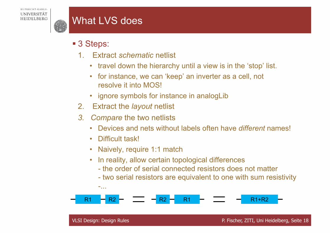
What LVS does
§ 3 Steps: 1. Extract schematic netlist
• travel down the hierarchy until a view is in the ‘stop’ list. • for instance, we can ‘keep’ an inverter as a cell, not
resolve it into MOS! • ignore symbols for instance in analogLib
2. Extract the layout netlist 3. Compare the two netlists
• Devices and nets without labels often have different names! • Difficult task! • Naively, require 1:1 match • In reality, allow certain topological differences
- the order of serial connected resistors does not matter - two serial resistors are equivalent to one with sum resistivity -...
VLSI Design: Design Rules P. Fischer, ZITI, Uni Heidelberg, Seite 18
R1 R2 R2 R1 R1+R2
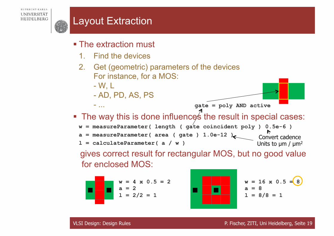
Layout Extraction
§ The extraction must 1. Find the devices 2. Get (geometric) parameters of the devices
For instance, for a MOS: - W, L - AD, PD, AS, PS - ... gate = poly AND active
§ The way this is done influences the result in special cases: w = measureParameter( length ( gate coincident poly ) 0.5e-6 ) a = measureParameter( area ( gate ) 1.0e-12 ) l = calculateParameter( a / w )
gives correct result for rectangular MOS, but no good value for enclosed MOS:
VLSI Design: Design Rules P. Fischer, ZITI, Uni Heidelberg, Seite 19
Convert cadence Units to µm / µm2
w = 16 x 0.5 = 8 a = 8 l = 8/8 = 1
w = 4 x 0.5 = 2 a = 2 l = 2/2 = 1

Example for 1:1 match
VLSI Design: Design Rules P. Fischer, ZITI, Uni Heidelberg, Seite 20
Schematic Extracted schematic netlist:
* 2 instances i M1 P_18_MM out in vdd! vdd! L 1.8e-07 M 1 W 8.8e-07 i M0 N_18_MM out in gnd! gnd! L 1.8e-07 M 1 W 4.4e-07
Layout Extracted layout netlist:
* 2 instances i av1 N_18_MM out in gnd! gnd! l 1.8e-07 w 4.4e-07; i av2 P_18_MM out in vdd! vdd! l 1.8e-07 w 8.8e-07;
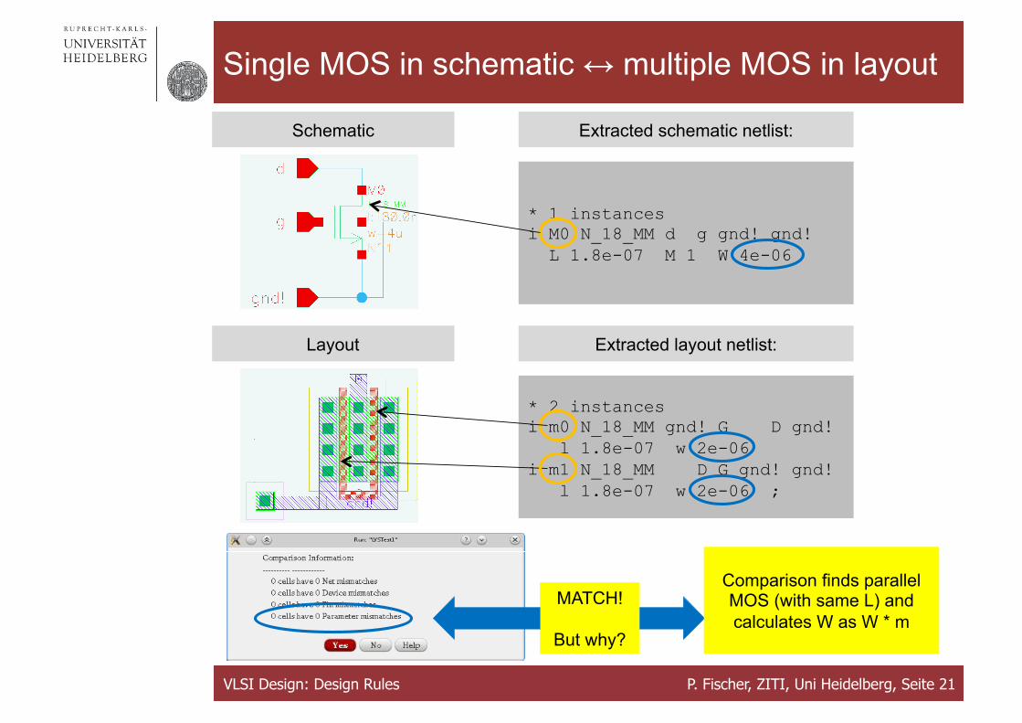
Single MOS in schematic ↔ multiple MOS in layout
VLSI Design: Design Rules P. Fischer, ZITI, Uni Heidelberg, Seite 21
Schematic Extracted schematic netlist:
* 2 instances i m0 N_18_MM gnd! G D gnd! l 1.8e-07 w 2e-06 i m1 N_18_MM D G gnd! gnd! l 1.8e-07 w 2e-06 ;
Layout Extracted layout netlist:
* 1 instances i M0 N_18_MM d g gnd! gnd! L 1.8e-07 M 1 W 4e-06
MATCH!
But why?
Comparison finds parallel MOS (with same L) and calculates W as W * m
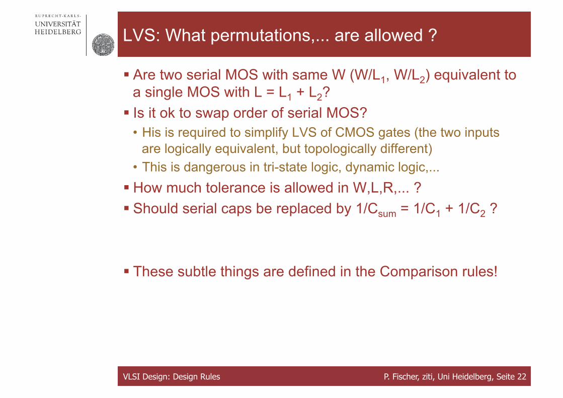
LVS: What permutations,... are allowed ?
§ Are two serial MOS with same W (W/L1, W/L2) equivalent to a single MOS with L = L1 + L2?
§ Is it ok to swap order of serial MOS? • His is required to simplify LVS of CMOS gates (the two inputs
are logically equivalent, but topologically different) • This is dangerous in tri-state logic, dynamic logic,...
§ How much tolerance is allowed in W,L,R,... ? § Should serial caps be replaced by 1/Csum = 1/C1 + 1/C2 ?
§ These subtle things are defined in the Comparison rules!
VLSI Design: Design Rules P. Fischer, ziti, Uni Heidelberg, Seite 22
Top Related