


Languages
Pages
Legal


Design Challenges for Ultra-Wide Band Radio
Sudhir Aggarwal2
J. Bergervoet1, K.S. Harish1, G. van der Weide1, D. Leenaerts1, R. van de Beek1, R. Roovers1
C. Razzell2, Y. Zhang2, H. Waite2
1Philips Research, 2Philips SemiconductorsSan Jose, CA USA
June 16,2005

Semiconductors, Sudhir Aggarwal et al. 2
Contents
• Introduction to UWB• Why we need UWB?• UWB Signals• MBOA Proposal• Design Challenges• Receiver Implementation• Results• Conclusions

Semiconductors, Sudhir Aggarwal et al. 3
Contents
• Introduction to UWB• Why we need UWB?• UWB Signals• MBOA Proposal• Design Challenges• Receiver Implementation• Results• Conclusions

Semiconductors, Sudhir Aggarwal et al. 4
What is Ultra Wideband?
• FCC Definition– Signals must occupy a bandwidth > 500MHz– Or signal bandwidth 20% of the carrier frequency
• FCC recently opened up new spectrum for ultra-wideband transmissions– One of the bands is from 3.1GHz to 10.6GHz– Maximum power emission limit is –41.3dBm/MHz
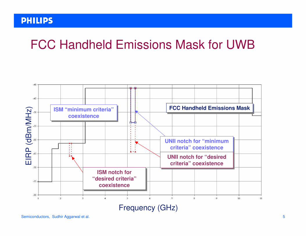
Semiconductors, Sudhir Aggarwal et al. 5
FCC Handheld Emissions Mask for UWBE
IRP
(dB
m/M
Hz) FCC Handheld Emissions MaskFCC Handheld Emissions MaskISM “minimum criteria”
coexistenceISM “minimum criteria”
coexistence
ISM notch for “desired criteria”
coexistence
ISM notch for “desired criteria”
coexistence
UNII notch for “minimum criteria” coexistence
UNII notch for “minimum criteria” coexistence
UNII notch for “desired criteria” coexistence
UNII notch for “desired criteria” coexistence
Frequency (GHz)

Semiconductors, Sudhir Aggarwal et al. 6
Generic channel capacity
• C=B.log2(1+SNR)
Capacity per channel (bps) ∝ Bandwidth
Capacity per channel (bps) ∝ log(1+SNR)
1. Can increase bandwidth
2. Can increase SNR, use higher order modulations
3. Can increase number of channels using spatial separation (e.g., MIMO)

Semiconductors, Sudhir Aggarwal et al. 7
Capacity vs. range for UWB & WLAN
This segment is for WPAN
(Assumes 20MHz WLAN, 1GHz UWB bandwidth)������������

Semiconductors, Sudhir Aggarwal et al. 8
Expected data rates and ranges for UWB wireless PANs
2.6 m 7.8 m480Mbps6.3 m14.1 m200Mbps
10.7 m20.5 m110MbpsCM2AWGNRate
MB-OFDM rates and ranges:

Semiconductors, Sudhir Aggarwal et al. 9
Standards : Range and Data Rate
Data Rate (Mbps)
Ran
ge
ZigBee UWB802.15.3aWPAN
10M
WLAN30M
WMAN(Fixed)
Cellular(Mobile)
WiFi
IEEE 802.16
2G
0.01 0.1 1 10 100 1000
Bluetooth
3G
���������������

Semiconductors, Sudhir Aggarwal et al. 10
Contents
• An introduction to UWB• Why we need UWB?• UWB Signals• MBOA Proposal• Design Challenges• Receiver Implementation• Results• Conclusions

Semiconductors, Sudhir Aggarwal et al. 11
Why UWB? - High Data RateNeed for fast video streaming• Wireless USB - 480 Mbps wirelessly• USB Mass Storage Application
Advantages
• Reduced installation costs
�Build on current drivers
• Portability
• Simplicity of use
• Easy connectionsbetween several sources
• No “non-standard”card interface concerns

Semiconductors, Sudhir Aggarwal et al. 12
Why UWB? Audio Files
• Need for Speed: AudioMP3 Music Download/Check-out:
For “Checking-out” (5MB/musicx15)• 10 Mbps (net) takes 1 minute ���� Boring• 300 Mbps (net) takes 2 seconds ���� Exhilarating !
CD Download/Check-out:
– 74 Minute audio takes ~700 MB– For “Checking-out”
• 10 Mbps (net) takes 10 minutes ���� Boring• 300 Mbps (net) takes 19 seconds ���� Exhilarating!

Semiconductors, Sudhir Aggarwal et al. 13
Why UWB? Image Files
• Need for Speed: Still Image
Digital Still Image Download/Upload:
– 128 MB Memory Stick Accommodates 80 Pictures• 15 Mbps (net) takes 60 seconds � Not Acceptable• 300 Mbps (net) takes 3 seconds � Instant

Semiconductors, Sudhir Aggarwal et al. 14
Contents
• An introduction to UWB• Why we need UWB?• UWB Signals• MBOA Proposal• Design Challenges• Receiver Implementation• Results• Conclusions

Semiconductors, Sudhir Aggarwal et al. 15
Signal bandwidth
~1/Tp (GHz)Tp (nS)
Ts ~1/Ts
Time Frequency

Semiconductors, Sudhir Aggarwal et al. 16
Ultra-Wide Bandwidth Signals
1. Use ultra-narrow pulses2. Use very fast direct sequence spread spectrum3. OFDM4. Multi-band sequencing/hoping

Semiconductors, Sudhir Aggarwal et al. 17
1.1 Ultra-narrow pulses (impulse radio)
mτ1∝
0ω
Basic Gaussian monopulse Pulse shape to meet FCC mask

Semiconductors, Sudhir Aggarwal et al. 18
1.2 Practical Issues with Impulse Radio
• Due to very narrow pulse width (0.1-1ns):– Very accurate timing generator needed– Very high DAC and ADC sampling rates needed
• E.g., 20,000,000,000 samples per second!– Channel matched filter needs to be very long to
capture all the significant channel energy– Channel estimation algorithm is complex – Impulse response of antenna plays a significant role
in shaping the transmitted pulse (regulatory and practical issues)

Semiconductors, Sudhir Aggarwal et al. 19
2. Ultra-Fast Direct Sequence• Approach uses direct-sequence spread spectrum techniques• Pulse filtering/shaping used with BPSK/QPSK modulation
– 50% excess bandwidth, root-raised-cosine impulse response
• Overall approach is similar to UMTS/3GPP cellular, except that Walsh codes are replaced by a ternary codes of length 24 or 32
114 or 85.5 MS/s
24 or 32 chips/symbol
2.736 GHz(±1 MHz, ± 3 MHz)
2.736 GHzHighBand
57 or 42.75 MS/s
24 or 32 chips/symbol
1.368 GHz(±1 MHz, ± 3 MHz)
1.368 GHzLowBand
Symbol RateCode LengthChip RateRRC BW

Semiconductors, Sudhir Aggarwal et al. 20
3. Ultra wideband signals using OFDM
• Orthogonal Frequency Division Multiplexing– Can efficiently multiplex many sub-carriers to occupy
~500MHz of spectrum– OFDM intrinsically deals with multipath issues by
keeping the symbol rate low (e.g., 3.2MHz)– Technology derived from 802.11a
• But only supports QPSK, not 16-QAM nor 64-QAM• Uses less ADC precision and lower arithmetic precision than
802.11a/g signal processing

Semiconductors, Sudhir Aggarwal et al. 21
4. Multi-band Sequencing / Hopping
• Apply divide-and-conquer approach
• Each sub-band requires lower rate ADC to digitize
• Length of digital filters needed for channel equalization is divided by N.
• Complexity reduction requires sequential use of bands

Semiconductors, Sudhir Aggarwal et al. 22
Contents
• An introduction to UWB• Why we need UWB?• UWB Signals• MBOA Proposal• Design Challenges• Receiver Implementation• Results• Conclusions

Semiconductors, Sudhir Aggarwal et al. 23
UWB frequency bands- MBOA
DS UWB

Semiconductors, Sudhir Aggarwal et al. 24
MBOA uses sequenced multiband approach to enhance OFDM
����
����� ��
���
���
����
����
�������
������ � ������������ ��!�" # $%# �& ' ��()��*
" ���
�+����� , ��!-.����/
0���!��1�� ������
��������

Semiconductors, Sudhir Aggarwal et al. 25
Example OFDM UWB Tx chain
DACScramblerConvolutional
EncoderPuncturer
BitInterleaver
ConstellationMapping
IFFTInsert Pilots
Add CP & GI
Interleaving Kernel
exp(j2πfct)
InputData
128 pt IFFT in 312.5ns528 MHz
507.35MHz
128 pt IFFT, 100 QPSK data tones, 12 pilots

Semiconductors, Sudhir Aggarwal et al. 26
OFDM Advantages
MBOA implementation requires 128-pt complex FFT every 312.5ns
• At 102.4MHz clock, this FFT requires– 40 real multipliers, 48 real adders per clock cycle
• 40 real multipliers, compared to 400 required in Rake receiver for DS UWB
• The proposed OFDM symbol deals with up to 60.6ns of delay spread while DS UWB covers only 40ns delay spread

Semiconductors, Sudhir Aggarwal et al. 27
Contents
• An introduction to UWB• Why we need UWB?• UWB Signals• MBOA Proposal• Design Challenges• Receiver Implementation• Results• Conclusions

Semiconductors, Sudhir Aggarwal et al. 28
Design Challenges – implementation choice
• SiGe radio vs. All CMOS RF/BB?– Several startups, plus TI and Intel focus on CMOS
solutions– MB-OFDM is designed to be “CMOS friendly”
• Use of 2x oversampling in DACs and ADCs may be too power hungry (e.g., 150mW)– Several implementations known to be using 1x
oversampling• Power consumption needs to be balanced with robust
handling of large signal interferers

Semiconductors, Sudhir Aggarwal et al. 29
in
• Distance wanted UWB: 10.0m (-73dBm)• Distance 802.11a interferer: 0.2m (-3dBm)• Distance 2.4GHz ISM interferer: 0.2m (-8dBm)• Distance unwanted UWB interferer: 2.0m (-60dBm)
2450 5800
UWB
Freq (MHz)
70dB65dB
3432 3960 4488
Interferer scenario: (MBOA recommendation)
Interferer attenuation by pre-filter: 20-30dB
Design Challenges - system
P UnwantedUWB

Semiconductors, Sudhir Aggarwal et al. 30
Design Challenges - circuits
• Broadband LNA– NF=3dB, G=15dB, OIP3=+10dBm, BW=1.6GHz min., – Notch@ 5GHz, antenna interface
• Filter/VGA– BW: >250MHz– 3rd order or higher
• ADC– 1GS/s
• Multi-tone LO– LO must be able to hop in less than 9nS.

Semiconductors, Sudhir Aggarwal et al. 31
Contents
• An introduction to UWB• Why we need UWB?• UWB Signals• MBOA Proposal• Design Challenges• Receiver Implementation• Results• Conclusions

Semiconductors, Sudhir Aggarwal et al. 32
Receive chain: requirements and implementation
• Noise figure: < 6 dB• Input IP2: > +15 dBm• Input IP3: > -9 dBmrnal5th order IF filter (> 55dB Attenuation @ 660MHz)
≈≈
3432 MHz/3960 MHz/4488 MHz
Multitonegenerator
LNA≈
≈
Pre-filterBB amplifier/filter
I
Q
ADC
Zero IF receive chain
mixer

Semiconductors, Sudhir Aggarwal et al. 33
Single-ended LNA with high linearity
• Emitter degeneration coil (option a) would have to be very large.• Circuit b) gives simultaneous noise and power matching using current feedback (R) and voltage feedback (transformer).• Transformer is in fact area-friendly compared with coil alone:
Le Tfm.
R

Semiconductors, Sudhir Aggarwal et al. 34
RF in
I Q
LO
Tr
Q2
Q1
Q3
Q4R1
Vcc
C1
Implementation of LNA plus mixer(biasing components not shown)
LNA Mixer

Semiconductors, Sudhir Aggarwal et al. 35
Passiveswitched attenuator
Digital gain control -30 to 0 dB in 6dB steps Capacitive tuning of
bandwidth and Quality Factor
DC offset compensation
R/Cnetwork
I - Base-band filter amplifier
Q - Base-band filter amplifier
R/C feedbacknetwork
R/C feedbacknetwork
R/C feedbacknetwork
R/C feedbacknetwork
R/C feedbacknetwork
R/C feedbacknetwork
Baseband Filter/Amplifier
In Out

Semiconductors, Sudhir Aggarwal et al. 36
V
(e.g.:Heinlein and Holmes, “Active Filters for Integrated Circuits.”)
•Not all components required for each stage.•One stage can give at most two poles and two zeros (bi-quadratic).•Good channel selection can be obtained.
Base-band filter stage
Rauch filter, general:
s-plane
outV in

Semiconductors, Sudhir Aggarwal et al. 37
Proposed LO Implementation
PLL ÷2
PLL2G
PLL ÷2
÷2
SSBI
Q
I Q
7.92 GHz
2.112 GHz
3960 MHz
-528 MHz/0/
+528 MHz
FilterFrequencySelector
3432 MHz/3960 MHz/4488 MHz44 MHz
≈≈
PLL8G
Third order harmonic of 528MHz:MHzMHzMHz 554452833960 =⋅+
MHzMHzMHz 237652833960 =⋅−Spur issue

Semiconductors, Sudhir Aggarwal et al. 38
Contents
• An introduction to UWB• Why we need UWB?• UWB Signals• MBOA Proposal• Design Challenges• Receiver Implementation• Results• Conclusions

Semiconductors, Sudhir Aggarwal et al. 39
RF input
BB filter BB outputs
Multitonegenerator
LNA mixer
Chip photo2
mm
(fT =70GHz SiGe BiCMOS)

Semiconductors, Sudhir Aggarwal et al. 40
Phase Noise Measurement
Phase Noise for band #3 < 0.5°°°° rms
-95dBc/Hz -104dBc/Hz@1MHz

Semiconductors, Sudhir Aggarwal et al. 41
Spurs Measurement
LO leakageImage
4488MHz
3960MHz
3432MHz
3960+2*528
3960+3*528
2376MHz50dBc
3960-3*528

Semiconductors, Sudhir Aggarwal et al. 42
Switching Time Measurement
Calculate FFT to measure the switching time
Hopping from band #1 to #3
For all hopping scenarios:Settling time below 1ns.
1ns
output
control

Semiconductors, Sudhir Aggarwal et al. 43
system:
NF
S21
S12
S11 (measured on PCB)
[GHz]
[dB]
For 3-band
Measured LNA characteristics
S11(chip)

Semiconductors, Sudhir Aggarwal et al. 44
system
NF
[GHz]
[dB]
3-band
S11(chip)
Measured LNA results (recentered design shown in red!)
S21
Increased LNA gain, for better overall system noise figure!
Old
New

Semiconductors, Sudhir Aggarwal et al. 45
-2000 -1500 -1000 -500 0 500 1000 1500 2000-80
-60
-40
-20
0
20
40
60
Frequency (MHz)
Gai
n (d
B)
Attenuation steps[0,6,12,18,24,30 dB]
660MHz
Simulated response
Measured response
0 100 20038
40
42
44
46
Frequency (MHz)
Gai
n (
dB
)
Q Tuning
5.3dB
0 100 200 30030
35
40
45
Frequency (MHz)
Gai
n (
dB
)
Bandwidth Tuning
25MHz57.9dB
Measured baseband filter response

Semiconductors, Sudhir Aggarwal et al. 46
Band#2 to Band#1 or Band#3
1nSLO Hoping time
Receiver chain, LO generator
2.5V, 47mA,27mA
Supply
fin1 : 5 GHz ISM,fin2 : 802.11a
-7 dBmInput IP3
fin1 : 5 GHz ISM, fin2 : 2.4 GHz ISM
+16 dBmInput IP2
power gain from RF input to BB output
62 dBGain
On PCB, center of band, fLO=4GHz
5 dB Noise figure
Summary of RX system measured parameters

Semiconductors, Sudhir Aggarwal et al. 47
Contents
• An introduction to UWB• Why we need UWB?• UWB Signals• MBOA Proposal• Design Challenges• Receiver Implementation• Results• Conclusions

Semiconductors, Sudhir Aggarwal et al. 48
Conclusions
• A low power fast-hopping (<1nS) synthesizer for UWB radio is demonstrated
• A UWB radio can be designed to be robust to the interference of the existing WLAN wireless devices
• A UWB radio using large bandwidth is possible at low power offering opportunity to exploit Shannon’s capacity formula for high data rates
• UWB technology is ripe for exploitation to achieve high data rates for WPAN applications.

Top Related