


Languages
Pages
Legal


CSE241 L20 Futures .1 Kahng, UCSD ©2003
CSE241VLSI Digital Circuits
Winter 2003
Lecture 20: Futures for VLSI

CSE241 L20 Futures .2 Kahng, UCSD ©2003
Topic List: ReviewWeek 1: MOSFETs, interconnects, R/C/L, performance, power, Verilog
Week 2: ASIC flow, design planning/convergence methodologies, key design challenges, STA, datapath blocks, performance coding
Week 3: Logic synthesis (covering, technology mapping, local transformations), synthesis, timing
Week 4: Timing, clocking, clock distribution, timing libraries, project announcement (v.1), synthesis for timing, placement
Week 5: Routing, place-and-route, IBM ACG placement, STA lab(PrimeTime)
Week 6: Power distribution, noise analysis, parasitic extraction, P&R lab(SE), project announcement (v. 2)
Week 7: Verification, formal verification lab, manufacturing and manufacturability
Week 8: Manufacturability, SDF back-annotation into PrimeTime
Week 9: Packaging, cost
Week 10: Memory blocks, VLSI futures

CSE241 L20 Futures .3 Kahng, UCSD ©2003
LogisticsToday’s class:
Where the BIG research challenges arePower-centric view of VLSI futuresReferences:- A. B. Kahng, “A Roadmap and Vision for Physical Design”, Proc. ISPD,
April 2002. http://vlsicad.ucsd.edu/Publications/Conferences/c136.pdf- D. Sylvester and H. Kaul, “Performance Challenges in Nanometer
Design”, Proc. DAC, June 2001.
Class ends at 10:30am
Will have OH’s on Monday
Will broadcast ABK project current status by Sunday night
Any logistics questions, send email
CSE241 L20 Futures .4 Kahng, UCSD ©2003
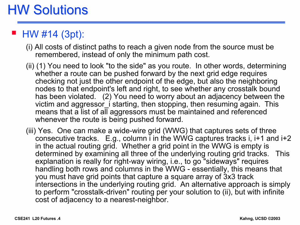
HW SolutionsHW Solutions
HW #14 (3pt):(i) All costs of distinct paths to reach a given node from the source must be
remembered, instead of only the minimum path cost.(ii) (1) You need to look "to the side" as you route. In other words, determining
whether a route can be pushed forward by the next grid edge requires checking not just the other endpoint of the edge, but also the neighboring nodes to that endpoint's left and right, to see whether any crosstalk bound has been violated. (2) You need to worry about an adjacency between the victim and aggressor_i starting, then stopping, then resuming again. This means that a list of all aggressors must be maintained and referenced whenever the route is being pushed forward.
(iii) Yes. One can make a wide-wire grid (WWG) that captures sets of three consecutive tracks. E.g., column i in the WWG captures tracks i, i+1 and i+2 in the actual routing grid. Whether a grid point in the WWG is empty is determined by examining all three of the underlying routing grid tracks. This explanation is really for right-way wiring, i.e., to go "sideways" requires handling both rows and columns in the WWG - essentially, this means that you must have grid points that capture a square array of 3x3 track intersections in the underlying routing grid. An alternative approach is simply to perform "crosstalk-driven" routing per your solution to (ii), but with infinite cost of adjacency to a nearest-neighbor.

CSE241 L20 Futures .5 Kahng, UCSD ©2003
HW SolutionsHW SolutionsHW #15 (3pt):
(i) The end-case placement assumes that the whitespace in the instance is evenly distributed. This is suboptimal.
(ii) (Give data from a netlist.) You should have found that quite a few nets have 2 and 3 pins (at least 40%). This percentage is growing since there are more inserted repeaters, weaker drivers (and increasing ratio of interconnect R to driver R), etc. as technology scales.
(iii) Some ideas are: (1) fanout limits, (2) output load capacitance limits, (3) output slew time limits, and (4) artificially tweaking the pin input caps in the library (to some extent, increasing per-unit length wire cap will also tend to reduce fanouts).
HW #16 (2pt):(a) There are 4 internal nodes of the slicing tree, of which the first (root) is horizontal. The
other 3 internal nodes can be either H or V, implying 23 = 8 possibilities. There are also 5 total blocks, each of which can be put into two orientations, implying another factor of 25 = 32. What is the number Ak of distinct slicing floorplans for k blocks? Actually, this does get kind of tedious. By hand: A1 = 1, A2 = 2, A3 = 6, A4 = 22. Trying to find previous results on Google leads to Catalan numbers (for binary trees) and thence to super-Catalan numbers. A recurrence is given by B. Yao, H. Chen, C.-K. Cheng and R. Graham (of UCSD), in their ISPD-2001 paper. In particular, A5 = 90. Multiply by 28 to obtain the answer.
(b) Ak is the kth super-Catalan or Schroder number (see the given reference). (The main conclusion is that the number of floorplans grows rapidly with k, and hence it is difficult to optimize over all floorplans. This is one reason why no one has yet claimed my car as a prize from the open challenge made in April 2000.)

CSE241 L20 Futures .6 Kahng, UCSD ©2003
HW SolutionsHW SolutionsHW #17:(a) (2pt) Increase the percentiles that determine the WLM: More wires will be
treated pessimistically, and hence more cell area, buffer area, and power will be used. Decrease the percentiles that determine the WLM: Fewer wires will be treated pessimistically, and less area and power will be used, but there is a higher likelihood that the design will fail to meet timing in place-and-route.(There is an interesting interaction between fanout, place-and-route, and WLM. If we believe that synthesis makes a high-fanout net only when the net does not affect critical paths, and if we further believe that timing-driven place-and-route does not carefully minimize wirelength of non-critical nets, then it is probably good to treat high-fanout nets pessimistically (thisguardbands the assumption that we believe the synthesis tool is making). On the other hand, if we believe that synthesis makes a low-fanout net when the net is critical, and if we further believe that TD P&R more carefully minimizes the length of critical nets, then we might be more optimistic with the WLM for low-fanout nets.)Increase the clock frequency target: more buffers and higher-drive cells will be used, which actually increases the area of the design (eventually making wires longer, and timing harder to meet). So, the benefits of this technique eventually run out of steam. Decrease the clock frequency target: not applicable (would never do this in hopes of making timing).
(b) (3pt) (Back up with evidence from P&R runs.)

CSE241 L20 Futures .7 Kahng, UCSD ©2003
MT SolutionsMT Solutions
#1(a) My basic flow: (1) SC global placement, (2) post-placement STA, (3) clock sink useful-skew scheduling, (4) clock buffer tree construction that is useful-skew aware (cf. “associative skew”), (5) standard-cell ECO placement (to put the buffers into the layout), (6) Steiner clock subnet routing at lower levels of the clock tree (following CTGen type paradigm), (7) bounded-skew clock subnet routing at all higher levels of the clock tree, and as necessary even at lower levels, to enforce useful skews, (8) global signal routing, (9) detailed signal routing, (10) post-detailed routing STA
#1(b) Criteria: (1) likelihood of convergence with maximum clock frequency, (2) minimization of CPU time (by maximizing incremental steps, minimizing “detailed” steps, and minimizing iterations), (3) make a good tradeoff between wiring-based skew control and wire cost (this suggests Steiner routing at lower levels, bounded-skew routing at higher levels). [Comment 1. Criteria NOT addressed: power, insertion delay, variant flow for hierarchical clocking or gated clocking. Comment 2: I do not know of any technology for “clock sink placement” that can separate this from placement of remaining standard cells. So, my flow does not invoke this step. I also don’t want post-route ECOs.]
#1(c) Variants: (1) introduce Step 11: loop over Steps 3-10 (not adopted because cost-benefit ratio was not attractive, and because there is a trial placement + global routing to drive useful-skew scheduling, buffer tree construction and ECO placement); (2) after Steps 1-4, re-place the entire netlist (global, detailed placement) and then skip Step 5 (not adopted because benefits of avoiding ECO placement and leveraging a “good clock skeleton” were felt to be small – buffer tree will largely reflect the netlist structure, and re-placing can destroy assumptions made in Steps 3-4); (3) can iterate the first 5 steps essentially by iterating: clock sink placement, (ECO placement for legalization), (incremental) standard-cell (global + detailed) placement (not adopted because I feel that any objective for standalone clock sink placement would be very “fuzzy”, e.g., based on sizes of intersections of fanin/fanout cones of sequentially adjacent FFs)

CSE241 L20 Futures .8 Kahng, UCSD ©2003
MT SolutionsMT Solutions
#2 What happens every two technology nodes: (1) one more level of “H” is added (with WL = twice the WL used to implement the previous level of “H” total clock tree WL doubles); (2) the number of clock sinks and the number of buffers are each multiplied by 4; (3) frequency is multiplied by 4; (4) supply voltage is multiplied by (0.85) x (0.85) = 0.7225; and (5) the gate area of a given clock sink or buffer scales is reduced by a factor of 4 (0.7 ^ 4 = 0.24). In the analysis of CV2f power, V2f scales by (0.5) x (4) = 2x. Then, wire capacitance scales by 2x (roughly, assuming that areal and lateral caps combine to scale at 1x per unit wire length) while gate and buffer capacitance scale by 1x (assuming that WL/tox is roughly 1x instead of, say, 0.7x). Conclusion: power dissipation due to wiring multiplies by 4, and power dissipation due to clock sinks+buffers multiplies by 2. (It is also okay to argue that sinks+buffers power is constant.) This analysis also assumes that static power can be ignored, and does not dissect wire capacitance into area + fringing components. Also, there is no accounting for possible need for wider wires at the top levels of the clock tree (e.g., for process variation robustness at higher frequencies).
#3 The LEF file will remain roughly the same size (same richness of cell library, say, between 500-1200 masters), modulo possible changes in conventions (e.g., CTLF used to be a part of LEF) and modulo possible additional library model semantics (e.g., adding power modeling into LEF). The DEF file should at least double (the components and nets will double, but if there is extra routing complexity (more complex geometries, and more segments per connection due to antenna rules or badly scaling router heuristics) the DEF could grow significantly faster.

CSE241 L20 Futures .9 Kahng, UCSD ©2003
Project Logistics4 pages of report + pointers
Place your PDF report in ~projxx/public_html/ on VLSI CAD Lab machines, then e-mail a URL by midnight, Wednesday night (March 19th)Maximum of two pages for (A), and maximum of two pages for (B)- Minimum 10 point font, minimum 1-inch margins on all sides, US Letter
paper only. Only PDF will be read. Report contents:- History: When you first completed synthesis, when you first completed P&R,
when you first completed analyses (RSPF-based STA, FV) – where “first completed” means the first time that you obtained a well-formed output
- Final values of metrics: (A) Frequency, (B) Frequency / Area- CPU time, wall time and server type for flows used to obtain final metrics.- Assessment of methods that were (a) considered, (b) not tried (and why), (c)
tried (how, using the tools), and (d) were found most enabling (with justification of how this credit assignment was determined).
- Links to all final project files: runscripts, flow description (“README”), logfiles and journal files, report files (RCX, STA, FV, etc.), design files (.sv, .def). It will help to organize the project files and to put README files in each directory.
Points will be deducted for incorrect spelling, incorrect grammar, and other indications that you did not read over your own report!- Hint: MSWord has spelling and grammar checks; use these. Also, ask your
roommates/labmates/colleagues to read over your report before you turn it in.
CSE241 L20 Futures .10 Kahng, UCSD ©2003
The BIG Challenges

CSE241 L20 Futures .11 Kahng, UCSD ©2003
The “Red Brick Wall” - 2001 vs. 1999
Source: Semiconductor International - http://www.e-insite.net/semiconductor/index.asp?layout=article&articleId=CA187876

CSE241 L20 Futures .12 Kahng, UCSD ©2003
YEAR
TECHNOLOGY NODE
2001 2002 2003 2004 2005 2006 2007
DRAM ½ PITCH (nm) (SC. 2.0) 130 115 100 90 80 70 65
MPU/ASIC ½ PITCH (nm) (SC. 3.7) 150 130 107 90 80 70 65
MPU PRINTED GATE LENGTH (nm) (SC. 3.7) 90 75 65 53 45 40 35
MPU PHYSICAL GATE LENGTH (nm) (SC. 3.7) 65 53 45 37 32 28 25
Conductor effective resistivity(µΩ -cm) Cu intermediate wiring*
2.2 2.2 2.2 2.2 2.2 2.2 2.2
Barrier/cladding thickness(for Cu intermediate wiring) (nm)
18 15 13 11 10 9 8
Interlevel metal insulator—effective dielectric constant (κ)
3.0-3.7 3.0–3.7 2.9–3.5 2.5–3.0 2.5–3.0 2.5–3.0 2.0–2.5
Interlevel metal insulator (minimumexpected)—bulk dielectric constant (κ )
2.7 2.7 2.7 2.2 2.2 2.2 1.7
Red Brick Example: Dielectric Permittivity
C. Case, BOC Edwards – ITRS-2001
“Red Brick” = ITRS Technology Requirement with no known solution

CSE241 L20 Futures .13 Kahng, UCSD ©2003
SRC Grand Challenges1. Extend CMOS to its ultimate limit
2. Support continuation of Moore's Law by providing a knowledge base for CMOS replacement devices
3. Enable Wireless/Telecomm systems by addressing technical barriers in design, test, process, device and packaging technologies
4. Create mixed-domain transistor and device interconnection technologies, architectures, and tools for future microsystems that mitigate the limitations projected by ITRS
5. Search for radical, cost effective post NGL patterning options
6. Provide low-cost environmentally benign IC processes
7. Increase factory capital utilization efficiency through operational modeling
8. Provide design tools and techniques which enhance design productivity and reduce cost for correct, manufacturable and testable SOC's and SOP's
9. Enable low power and low voltage solutions for mobile/battery conserving applications through system and circuit design, test and packaging approaches.
10. Enable very low cost components
11. Provide tools enabling rapid implementation of new system architectures

CSE241 L20 Futures .14 Kahng, UCSD ©2003
SRC ICSS Key Technologies (Top 12)
SystemsS3.2: Early Design Space
Exploration S1.2: Low Power, Real-Time
Algorithms and Architectures S4.1: On-Chip Communication S1.3: High Bandwidth and/or
Low Power Communication S2.4: Deep Submicron Aware
Microarchitectures, Accounting for Noise, Power, Timing, Interconnects, etc.
S1.1: High Level Specifications of Complex Systems
CircuitsC1.2: Digital Low Power and/or
Low Voltage Circuit Design C2.1: Mixed Signal Circuits on
Advanced Technologies C2.4: Mixed Signal Low Power
and/or Low Voltage Circuit Design
C1.1: Digital Circuits on Advanced Technologies
C2.3: Mixed Signal Design for Test
C2.2: Mixed Signal Noise Immune and/or Tolerant Circuits
CSE241 L20 Futures .15 Kahng, UCSD ©2003
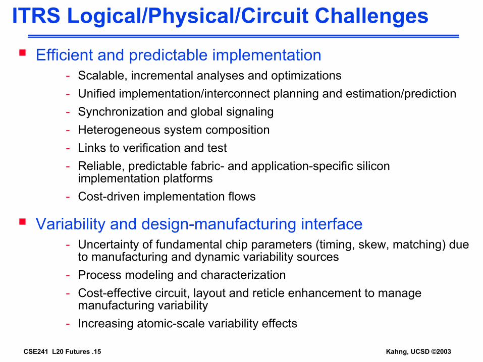
ITRS Logical/Physical/Circuit Challenges
Efficient and predictable implementation- Scalable, incremental analyses and optimizations- Unified implementation/interconnect planning and estimation/prediction- Synchronization and global signaling- Heterogeneous system composition- Links to verification and test- Reliable, predictable fabric- and application-specific silicon
implementation platforms- Cost-driven implementation flows
Variability and design-manufacturing interface- Uncertainty of fundamental chip parameters (timing, skew, matching) due
to manufacturing and dynamic variability sources- Process modeling and characterization- Cost-effective circuit, layout and reticle enhancement to manage
manufacturing variability- Increasing atomic-scale variability effects

CSE241 L20 Futures .16 Kahng, UCSD ©2003
Silicon complexity, non-ideal device scaling and power management
- Leakage and power management- Reliability and fault tolerance- Analysis complexity and consistent analyses / synthesis objectives- Recapture of reliability lost in manufacturing test
Circuit design to fully exploit device technology innovation- Support for new circuit families that address power and performance
challenges- Implementation tools for SOI- Analog synthesis- Increasing atomic-scale effects- Adaptive and self-repairing circuits- Low-power sensing and sensor interface circuits; micro-optical devices
ITRS Logical/Physical/Circuit Challenges
CSE241 L20 Futures .17 Kahng, UCSD ©2003
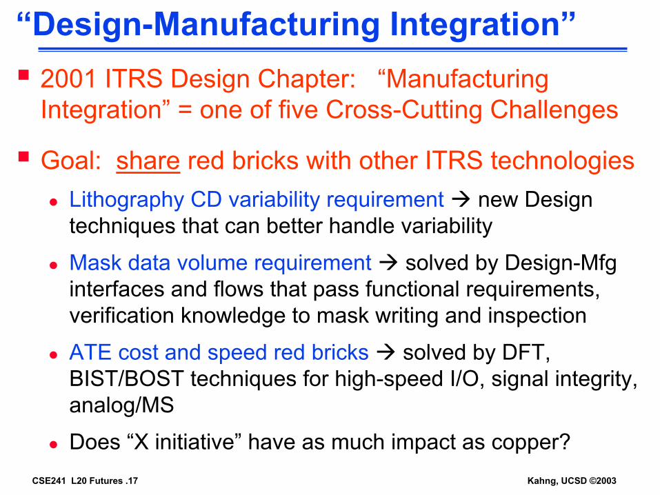
“Design-Manufacturing Integration”2001 ITRS Design Chapter: “Manufacturing Integration” = one of five Cross-Cutting Challenges
Goal: share red bricks with other ITRS technologiesLithography CD variability requirement new Design techniques that can better handle variability
Mask data volume requirement solved by Design-Mfg interfaces and flows that pass functional requirements, verification knowledge to mask writing and inspection
ATE cost and speed red bricks solved by DFT, BIST/BOST techniques for high-speed I/O, signal integrity, analog/MS
Does “X initiative” have as much impact as copper?
CSE241 L20 Futures .18 Kahng, UCSD ©2003
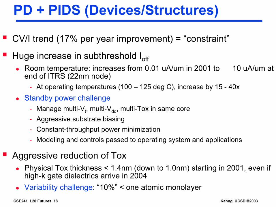
PD + PIDS (Devices/Structures)
CV/I trend (17% per year improvement) = “constraint”
Huge increase in subthreshold IoffRoom temperature: increases from 0.01 uA/um in 2001 to 10 uA/um at end of ITRS (22nm node)
- At operating temperatures (100 – 125 deg C), increase by 15 - 40xStandby power challenge
- Manage multi-Vt, multi-Vdd, multi-Tox in same core- Aggressive substrate biasing- Constant-throughput power minimization- Modeling and controls passed to operating system and applications
Aggressive reduction of ToxPhysical Tox thickness < 1.4nm (down to 1.0nm) starting in 2001, even if high-k gate dielectrics arrive in 2004Variability challenge: “10%” < one atomic monolayer

CSE241 L20 Futures .19 Kahng, UCSD ©2003
PD + Lithography10% CD uniformity is a red brick today
10% < 1 atomic monolayer at end of ITRS
This year: Lithography, PIDS, FEP agreed to raise CD uniformity requirement to 15% (but still a red brick)
Design for variabilityNovel circuit topologiesCircuit optimization (conflict between slack minimization and guardbanding of quadratically increasing delay sensitivity)Centering and design for $/wafer
Design for when devices, interconnects no longer 100% guaranteed correct?
Potentially huge savings in manufacturing, verification, test costs

CSE241 L20 Futures .20 Kahng, UCSD ©2003
PD + Assembly and PackagingGoal: cost control ($0.07/pin, $2 package, …)
“Grand Challenge” for A&P: work with Design to develop die-package co-analysis, co-optimization tools
Bump/pad counts scale with chip area onlyEffective bump pitch roughly constant at 300um MPU pad counts flat from 2001-2005, but chip current draw increases 64%
IR drop control challengeMetal requirements explode with Ichip and wiring resistance
Power challenge50 W/cm2 limit for forced-air cooling; MPU area becomes flat because power budget is flatMore control (e.g., dynamic frequency and supply scaling) given to OS and applicationLong-term: Peltier-type thermoelectric cooling, …

CSE241 L20 Futures .21 Kahng, UCSD ©2003
PD + Manufacturing TestHigh-speed interfaces (networking, memory I/O)
Frequencies on same scale as overall tester timing accuracy
Heterogeneous SOC designTest reuseIntegration of distinct test technologies within single deviceAnalog/mixed-signal test
Reliability screens failingBurn-in screening not practical with lower Vdd, higher power budgets
overkill impact on yield
Design challenges: DFT, BIST PD in the loop!Analog/mixed-signalSignal integrity and advanced fault modelsBIST for single-event upsets (in logic as well as memory)Reliability-related fault tolerance

CSE241 L20 Futures .22 Kahng, UCSD ©2003
How to Share Red BricksCost is the biggest missing link within the ITRS
Manufacturing cost (silicon cost per transistor)Manufacturing NRE cost (mask, probe card, …)Design NRE cost (engineers, tools, integration, …)Test costTechnology development cost who should solve a given red brick wall?
Return On Investment (ROI) = Value / CostValue needs to be defined (“design quality”, “time-to-market”)
Understanding cost and ROI allows sensible sharing of red bricks across industries

CSE241 L20 Futures .23 Kahng, UCSD ©2003
A Top-10 List(0) Sensible unifications to co-optimize global signaling, manufacturability enhancement, and clock/test/power distribution
(1) Fundamental new combinatorial optimization technologies (and possibly geometry engines) for future constraint-dominated layout regimes
(2) New decomposition schemes for physical design
(3) Global routing that is truly path-timing aware, truly combinatorial, and able to invoke “atomistic” interconnect synthesis
(4) In-context layout synthesis that maximizes process window while meeting electrical (functional) spec

CSE241 L20 Futures .24 Kahng, UCSD ©2003
A Top-10 List(5) Efficient analog and mixed-signal layout synthesis
(6) Methods for synchronization and global signaling at multi-GHz or –Gbps, extending to system-level
(7) Analysis, modeling and simulation methods that are tied more closely to PD syntheses, and that adapt to resource and accuracy and fidelity constraints
(8) Revival of platform-specific (parallel, distributed, hardware-accelerated) algorithm implementations
(9) Mindset changes, including a culture of “duplicating, deconstructing and debunking”

CSE241 L20 Futures .25 Kahng, UCSD ©2003
VLSI Futures

CSE241 L20 Futures .26 Kahng, UCSD ©2003
VLSI Futures (Power Focus)Many challenges in nanometer design
Signal integrity, RC delay, inductance (self and mutual), soft error rates, process variability (Vth control), reliable multi-GHz clock distribution, robust power distribution, designer productivity, etc.
Focus on POWERLow-power design = high-performance design
Key challenges in power:Affordable power removal: PackagingEfficient power management: DesignReliable power delivery: Distribution (not discussed today)
Start with a view of future high-speed (workstations, servers) microprocessors (MPUs)
D. Sylvester, DAC-2001

CSE241 L20 Futures .27 Kahng, UCSD ©2003
Working Model of High-Perf MPUs
A number of CPU cores (~10M transistors each) surrounded by numerous levels of caches (L1,L2,L3)
1-T SRAM or other “exotic” technologies may improve memory density and/or performanceMore cores == more work done == more power!Current example: IBM Power4 (2 CPU + 1.5-2MB L2); dissipates 115W in 3.8cm2 die
Power limits the computational capabilities of such a processor
CPU core
CPU core
Cache (L1 + L2), 2MB
CPU
Cache (L1, L2, L3), 16MB
CPU CPU
CPU CPU CPU2001 2007
D. Sylvester, DAC-2001

CSE241 L20 Futures .28 Kahng, UCSD ©2003
Less Performance Per Watt (Pollack’s Rule)
SPECfp Per Watt
0
0.5
1
1.5
2
2.5
3
3.5
May-1996
Dec-1996
Jun-1997
Jan-1998
Jul-1998
Feb-1999
Aug-1999
Mar-2000
Oct-2000
Apr-2001
Date of Data
New microarchitectures aren’t helping:40-70% better performanceAt the expense of 2-3X area! (power also higher)
Refs: specbench.org, Pollack, Gelsinger (Intel) D. Sylvester, DAC-2001
CSE241 L20 Futures .29 Kahng, UCSD ©2003
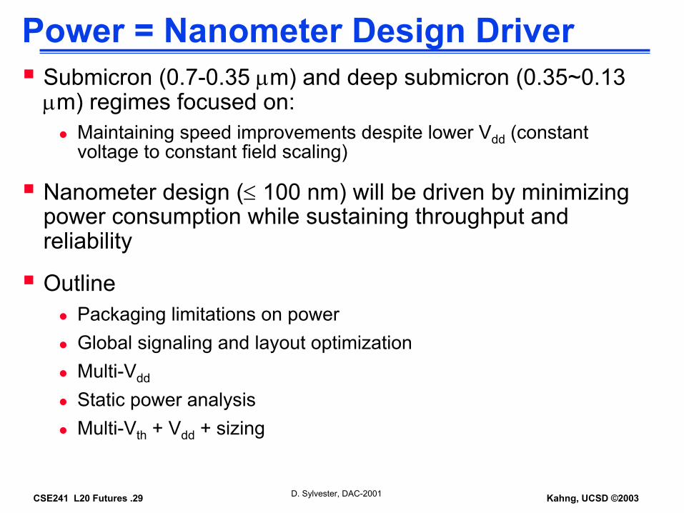
Power = Nanometer Design DriverSubmicron (0.7-0.35 µm) and deep submicron (0.35~0.13 µm) regimes focused on:
Maintaining speed improvements despite lower Vdd (constant voltage to constant field scaling)
Nanometer design (≤ 100 nm) will be driven by minimizing power consumption while sustaining throughput and reliability
OutlinePackaging limitations on powerGlobal signaling and layout optimizationMulti-Vdd
Static power analysisMulti-Vth + Vdd + sizing
D. Sylvester, DAC-2001

CSE241 L20 Futures .30 Kahng, UCSD ©2003
Packaging Limitations
Packaging limitations on powerGlobal signaling and layout optimization
Multi-Vdd
Static power analysis
Multi-Vth + Vdd + sizing
D. Sylvester, DAC-2001

CSE241 L20 Futures .31 Kahng, UCSD ©2003
Rising Power Density
Data taken from Intel, IBM, AMD, Compaq, Sun, ITRS2000
1997 1998 1999 2000 2001 2002 2003 2004
15
20
25
30
35
40
45
50
Pow
er D
ensi
ty (W
/cm
2 )
Year of Production
Equation governing the relationship among power, temperature, and packaging capabilities:
( ) chipambientchipja PTTθ −=
D. Sylvester, DAC-2001

CSE241 L20 Futures .32 Kahng, UCSD ©2003
Packaging and PowerTo maintain reasonable on-die (junction) temperatures, package thermal resistance must decrease
Cooling costs are highly non-linear with power consumption
Circuit reliability degrades (exponentially) with rising junction temperatures
Oxide lifetimeElectromigrationHot carrier effects
Performance also penalized by high operating temperatures
Slower transistorsHigher interconnect resistanceHigher leakage currents == higher total power
Power Density (W/cm2)
Cos
t ($)
~ 30-40W/cm2
( ) chipambientchipja PTTθ −=D. Sylvester, DAC-2001
CSE241 L20 Futures .33 Kahng, UCSD ©2003
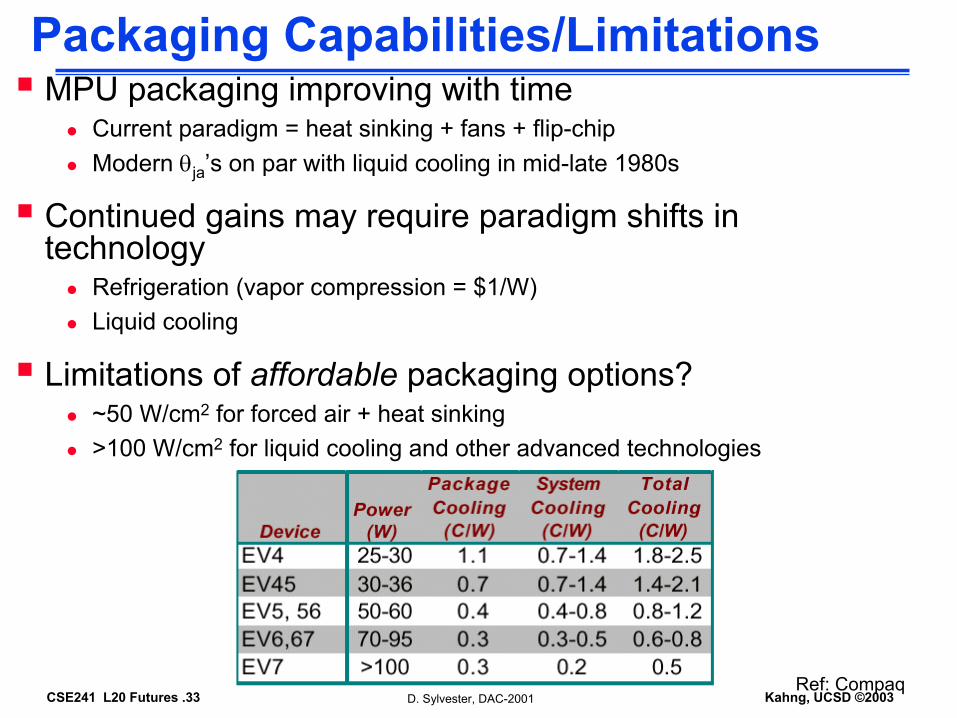
Packaging Capabilities/LimitationsMPU packaging improving with time
Current paradigm = heat sinking + fans + flip-chipModern θja’s on par with liquid cooling in mid-late 1980s
Continued gains may require paradigm shifts in technology
Refrigeration (vapor compression = $1/W)Liquid cooling
Limitations of affordable packaging options?~50 W/cm2 for forced air + heat sinking>100 W/cm2 for liquid cooling and other advanced technologies
Ref: CompaqD. Sylvester, DAC-2001
CSE241 L20 Futures .34 Kahng, UCSD ©2003
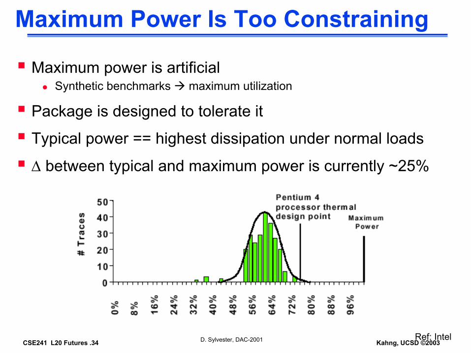
Maximum Power Is Too Constraining
Maximum power is artificialSynthetic benchmarks maximum utilization
Package is designed to tolerate it
Typical power == highest dissipation under normal loads
∆ between typical and maximum power is currently ~25%
Ref: IntelD. Sylvester, DAC-2001

CSE241 L20 Futures .35 Kahng, UCSD ©2003
Leveraging Typical vs. Maximum Power
Package design for maximum power wastes $$$
Better approach:Set thermal design point = largest commonly occurring power dissipation in typical applications, Ptypical
Design package to tolerate Ptypical (sustained)Apply dynamic thermal management techniques to restrict power to Ptypical
- Little performance loss as MPU rarely runs apps that exceed Ptypical
D. Sylvester, DAC-2001

CSE241 L20 Futures .36 Kahng, UCSD ©2003
Dynamic Thermal ManagementSimple hardware example: Intel P4 – compare current across a diode (temperature sensitive) to reference current source
Power flag reduces internal clock frequency, limiting power and temperature
Other approaches – voltage scaling, speculation control
Multiple sensors on large dies, placed in application-specific hot-spots
Power flag
Current comparator
Temperature sensing diode
Reference current source
D. Sylvester, DAC-2001

CSE241 L20 Futures .37 Kahng, UCSD ©2003
Global Signaling and Layout
Packaging limitations on power
Global signaling and layout optimization
Multi-Vdd
Static power analysis
Multi-Vth + Vdd + sizing
D. Sylvester, DAC-2001

CSE241 L20 Futures .38 Kahng, UCSD ©2003
Global Signaling
Current global signaling paradigm insert large static CMOS repeaters to reduce wire RC delay
Impending problems:Too many repeaters
- 180nm processors: 22K repeaters (Itanium), 70K (Power4)- Project 1-1.5M repeaters at 45-65nm technologies
Too much power- Many large repeaters = significant static and dynamic power
Too much noise- Repeater clustering complicates power distribution- Inductive coupling across wide bus structures
D. Sylvester, DAC-2001

CSE241 L20 Futures .39 Kahng, UCSD ©2003
Cell Layout OptimizationAdvanced layout techniques must allow
Continuous individual device sizingVariable p/n ratiosTapered FET stacking sizesArbitrary Vth assignments within gates
First cut: Cadabra 15-22% power reduction using 1st
two approaches under fixed footprint constraint
GDSII Import Compact fixed widthRef: Hurat, Cadabra
Optimize specific instances of
standard gates
D. Sylvester, DAC-2001
CSE241 L20 Futures .40 Kahng, UCSD ©2003
Multi-Vdd
Packaging limitations on power
Global signaling and layout optimization
Multi-VddStatic power analysis
Multi-Vth + Vdd + sizing
D. Sylvester, DAC-2001

CSE241 L20 Futures .41 Kahng, UCSD ©2003
Multi-Vdd Status
Idea: Incorporate two Vdd’s to reduce dynamic power
Limited to a few recent Japanese multimedia processorsExample – 0.3 µm, 75MHz, 3.3V media processor (Toshiba)
- Total power savings of 47% in logic, 69% in clockDynamic voltage scaling of mobile processors
- Transmeta Crusoe, Intel Speedstep, etc.- Not considered in this talk
Very powerful technique currently applied only inlow-performance designs
Mentality: today’s high performance parts aren’t “limited” by power
D. Sylvester, DAC-2001
CSE241 L20 Futures .42 Kahng, UCSD ©2003
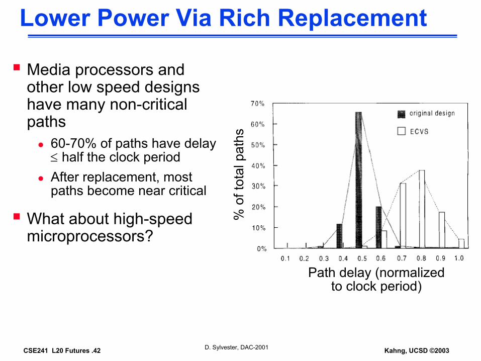
Lower Power Via Rich Replacement
Media processors and other low speed designs have many non-critical paths
60-70% of paths have delay ≤ half the clock periodAfter replacement, most paths become near critical
What about high-speed microprocessors?
% o
f tot
al p
aths
Path delay (normalized to clock period)
D. Sylvester, DAC-2001

CSE241 L20 Futures .43 Kahng, UCSD ©2003
Similar Story For High-Performance
IBM 480 MHz PowerPC shows over 50% of paths have delay less than half the clock period
Implies that high-performance designs can benefit from multi-Vdd
Ref: Akrout, JSSC98D. Sylvester, DAC-2001

CSE241 L20 Futures .44 Kahng, UCSD ©2003
Resizing Is Not The Right Answer
Post-synthesis optimizations resize gates to recover power on non-critical paths
Looks similar to pre- and post-replacement figures in media processor…
Before post-synthesis resizing
After post-synthesis resizing
Ref: Sirichotiyakul, DAC99
This is the wrong approach for nanometer design!
D. Sylvester, DAC-2001

CSE241 L20 Futures .45 Kahng, UCSD ©2003
Multi-Vdd Instead of Sizing
Power ~ C Vdd2 f, where f is fixed
Key: Reducing gate width impacts power sub-linearlyInterconnect capacitance is not affected
Reducing supply voltage cuts power quadraticallyAll capacitive loads have lower voltage swing
How can we minimize delay penalty at low Vdd?
D. Sylvester, DAC-2001

CSE241 L20 Futures .46 Kahng, UCSD ©2003
Challenges For Multi-Vdd
Area overheadToshiba reported 7% rise in area due to placement restrictions, level converters, additional power grid routing
EDA tool support for the above issues (placement, dual power routing)
Noise analysisAdditional shielding required between Vdd,low and Vdd,high signals?Including clock network
D. Sylvester, DAC-2001

CSE241 L20 Futures .47 Kahng, UCSD ©2003
Static Power
Packaging limitations on power
Global signaling and layout optimization
Multi-Vdd
Static powerMulti-Vth + Vdd + sizing
D. Sylvester, DAC-2001
CSE241 L20 Futures .48 Kahng, UCSD ©2003
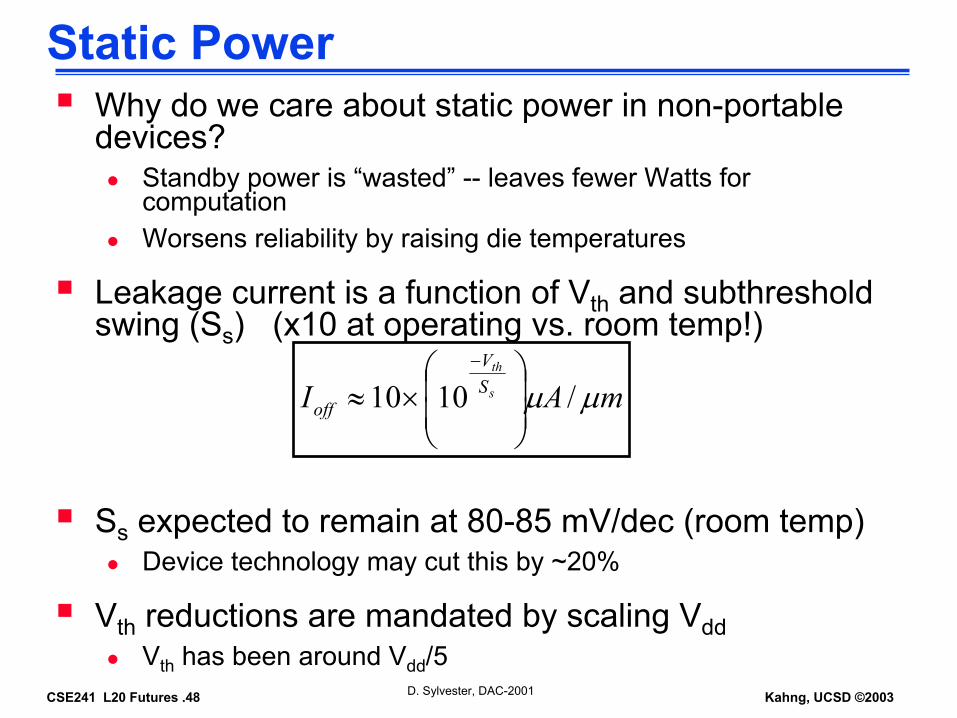
Static PowerWhy do we care about static power in non-portable devices?
Standby power is “wasted” -- leaves fewer Watts for computationWorsens reliability by raising die temperatures
Leakage current is a function of Vth and subthreshold swing (Ss) (x10 at operating vs. room temp!)
Ss expected to remain at 80-85 mV/dec (room temp)Device technology may cut this by ~20%
Vth reductions are mandated by scaling VddVth has been around Vdd/5
mAI s
thSV
off µµ /1010
×≈
−
D. Sylvester, DAC-2001
CSE241 L20 Futures .49 Kahng, UCSD ©2003
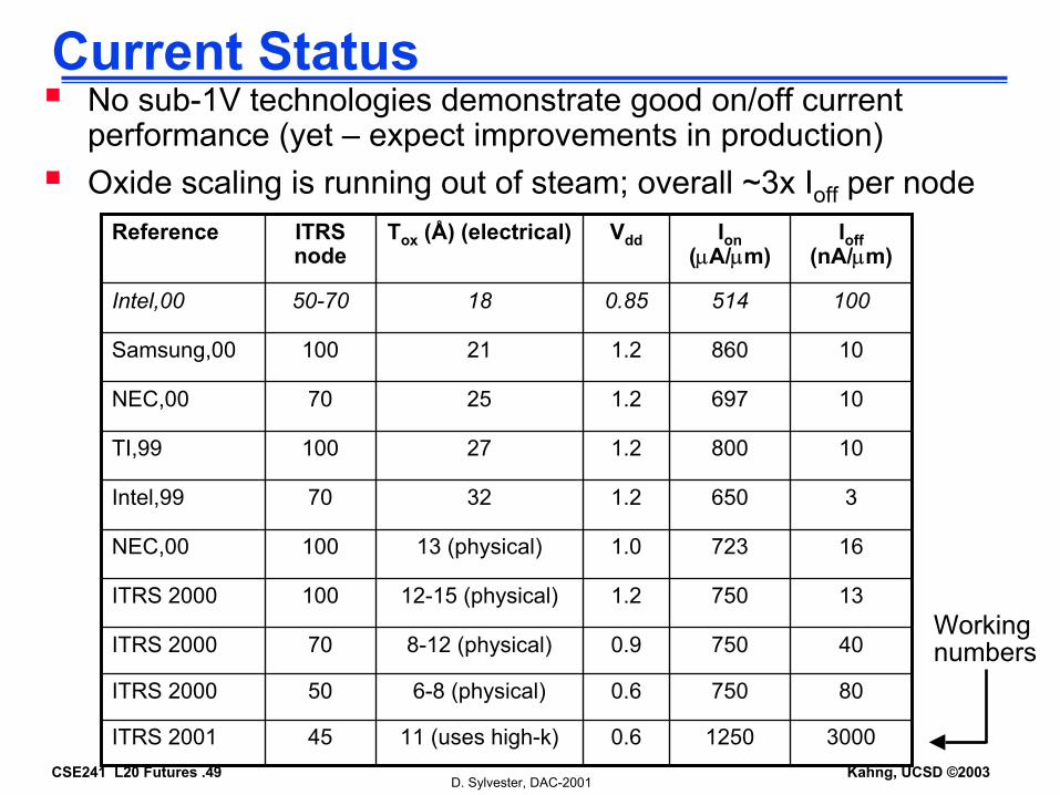
Current StatusNo sub-1V technologies demonstrate good on/off current performance (yet – expect improvements in production) Oxide scaling is running out of steam; overall ~3x Ioff per node
807500.66-8 (physical)50ITRS 2000
300012500.611 (uses high-k)45ITRS 2001
407500.98-12 (physical)70ITRS 2000
137501.212-15 (physical)100ITRS 2000
167231.013 (physical)100NEC,00
36501.23270Intel,99
108001.227100TI,99
106971.22570NEC,00
108601.221100Samsung,00
1005140.851850-70Intel,00
Ioff(nA/µm)
Ion(µA/µm)
VddTox (Å) (electrical)ITRS node
Reference
Working numbers
D. Sylvester, DAC-2001

CSE241 L20 Futures .50 Kahng, UCSD ©2003
Leakage Suppression Approaches
Dual-Vth (most common)Low-Vth on critical paths, high-Vth offOnly cost is additional masks
MTCMOSSeries inserted high-Vth device cuts leakage current when off (sleep mode)Delay and area penalties, control device sizing is critical
Other techniquesSubstrate biasing to control Vth
Dual-Vth domino- Use low-Vth devices only in
evaluate paths
Pull Up
Pull Down
ParasiticNode
Vcontrol
Vout
Vdd
High Vth Device
D. Sylvester, DAC-2001

CSE241 L20 Futures .51 Kahng, UCSD ©2003
Multi-Vth + Vdd + Sizing
Packaging limitations on power
Global signaling and layout optimization
Multi-Vdd
Static power analysis
Multi-Vth + Vdd + sizing
D. Sylvester, DAC-2001

CSE241 L20 Futures .52 Kahng, UCSD ©2003
Multi-Everything
Need an approach that selects between speed, static power, and dynamic power
Should be scalable to nanometer designRules out dual-Vth domino or other dynamic logic families (low supplies kill performance advantages)
Techniques mentioned so farFlexible, optimized cell layoutsMulti-Vdd
Dual-Vth
Put them all together
D. Sylvester, DAC-2001
CSE241 L20 Futures .53 Kahng, UCSD ©2003
Multi-Vdd Can Leverage Vth’s
Existing designs using multi-Vdd do not alter Vth in low-Vdd cells
Highly sub-optimal, delay is fully penalizedLimits cell replacement limits power savings
Much better solution: reduce Vth in low-Vdd cells to carefully balance delay, static power, and dynamic power
Enforce technology scaling within a chip – whenever we reduce Vdd, we also reduce Vth to maintain speed
D. Sylvester, DAC-2001

CSE241 L20 Futures .54 Kahng, UCSD ©2003
Multi-Vdd + Vth Negates Delay Penalty
0.2 0.3 0.4 0.5 0.6 0.7
1
2
3
4
1
2
3
4
35-nm, nominal Vdd = 0.6V
Constant Vth (0.11V) Scaled Vth, Constant Pstatic Conservatively Scaled Vth
Del
ay (N
orm
aliz
ed)
Vdd (V)
Delay ~ CVdd/Ion
ScenariosConstant Vth (current paradigm)Scale Vth to maintain constant static powerScale Vth to reduce static power linearly with Vdd
Delay penalty is substantially offset
Result: Vdd = 0.2V gives 89% dynamic power reduction, constant Pstatic, 29% delay increase
Ion is very sensitive to Vthat Vdd < 1VPstatic reduces with Vdd due to linear term and smaller Ioff (Ion and DIBL ⇓)
D. Sylvester, DAC-2001

CSE241 L20 Futures .55 Kahng, UCSD ©2003
Now Add Sizing
Multi-Vdd + multi-Vth + sizing/cell layout optimization attacks power from many angles (multi-dimensional)
Depending on criticality and switching activities, non-critical gates can be:
Assigned Vdd,lowAssigned Vdd,low + lower VthAssigned Vth,highDownsized (at the individual transistor level if advantageous)Assigned Vdd,low and upsized
- For gates that cannot tolerate Vdd,low delay, this can be power efficient
And others
D. Sylvester, DAC-2001

CSE241 L20 Futures .56 Kahng, UCSD ©2003
Intra-Cell Vth Assignments
Finer granularity of Vth assignmentAssigning top/bottom NMOS/PMOS in a stack to low-Vth(other devices high-Vth) balances speed and leakage
- 62% average leakage reduction compared to all-low Vth gate (3-in NAND)
- Worst-case delay is 7.2% faster than all-high Vth gate
Added manufacturing costs hard to quantify (stricter requirements on process recipes, longer process development times)
Still unclear whether this is beneficial and cost-effective
D. Sylvester, DAC-2001

CSE241 L20 Futures .57 Kahng, UCSD ©2003
SummaryPower density must saturate to maintain affordable packaging options
50 W/cm2 means 200-250W for future large MPUsDynamic thermal management saves 25% on packaging power budget
Multi-Vdd will leverage multiple Vth’s to offset delay penalty at low Vdd
More widespread re-assignment to Vdd,lowUse Vdd first instead of re-sizing to take advantage of large path slacksAnticipated power savings of 50-80%
Static power also addressed through multi-Vth + Vdd + sizing
Vth difficult to control in ultra-short channelsIntra-cell Vth assignment + MTCMOS/variants + sleep modes
D. Sylvester, DAC-2001

CSE241 L20 Futures .58 Kahng, UCSD ©2003
Conclusions
Future High-End MPUMany cores, lots of cache (possibly 1-T SRAM or eDRAM)Memory/logic breakdown is set by power density limitations (packaging/cost)
- By end of roadmap, <10% of chip will be logic- 20-40 CPU cores, up to 0.5 GB SRAM
Several Vdd’s and Vth’s 2 Vdd’s and 3 Vth’s are possibleAggressive use of sleep modes in both logic and memoryBreakdown of Pstatic and Pdynamic?? Optimal could be larger than we think: 30+% static power…Global communication using low-swing, current-steering, differential signaling fabricsProcess variation, particularly Vth control, will be crucialDesign tools must enable designers to implement all the above
D. Sylvester, DAC-2001
Top Related