


Languages
Pages
Legal


PIONEER CORPORATION 4-1, Meguro 1-Chome, Meguro-ku, Tokyo 153-8654, Japan PIONEER ELECTRONICS SERVICE INC. P.O.Box 1760, Long Beach, CA 90801-1760 U.S.A.PIONEER EUROPE NV Haven 1087 Keetberglaan 1, 9120 Melsele, Belgium PIONEER ELECTRONICS ASIACENTRE PTE.LTD. 253 Alexandra Road, #04-01, Singapore 159936
C PIONEER CORPORATION 2000 K-ZZY. NOV. 2000 Printed in Japan
ORDER NO.
CRT2589
MULTI-COMPACT DISC PLAYER
CDX-P670 X1N/EW
ServiceManual
- This service manual should be used together with the following manual(s):
Model No. Order No. Mech. Module Remarks
CX-892 CRT2356 C7 CD Mech. Module:Circuit Description, Mech. Description, Disassembly
CONTENTS
1. SAFETY INFORMATION ............................................3
2. EXPLODED VIEWS AND PARTS LIST .......................4
3. BLOCK DIAGRAM AND SCHEMATIC DIAGRAM ...12
4. PCB CONNECTION DIAGRAM ................................22
5. ELECTRICAL PARTS LIST ........................................28
6. ADJUSTMENT..........................................................31
7. GENERAL INFORMATION .......................................38
7.1 DIAGNOSIS ........................................................38
7.1.1 TEST MODE..............................................38
7.1.2 DISASSEMBLY .........................................44
7.1.3 CONNECTOR FUNCTION DESCRIPTION46
7.2 IC .........................................................................47
7.3 OPERATIONAL FLOW CHART...........................49
8. OPERATIONS AND SPECIFICATIONS.....................50

2
CDX-P670
A transport screw has been attached to the set in order to protectit during transportation. After removing the transport screw,cover the hole with the supplied seal. Be sure to remove thetransport screw before mounting the set. The removed transportscrew should be retained in the accessory bag for use the nexttime the set is transported.
Transport screwAttach to the original position before transporting the set.
SealAfter removing the transport screw, cover the holewith the supplied seal.
- CD Player Service Precautions
1. For pickup unit(CXX1285) handling, please refer
to"Disassembly"(see page 44).
During replacement, handling precautions shall be
taken to prevent an electrostatic discharge(protection
by a short pin).
2. During disassembly, be sure to turn the power off
since an internal IC might be destroyed when a con-
nector is plugged or unplugged.
3. Please checking the grating after changing the ser-
vice pickup unit(see page 32).
4. Since these screws protects the mechanism during
transport, be sure to affix it when it is transported for
repair, etc.

3
CDX-P670
1. Safety Precautions for those who Service this Unit.
• When checking or adjusting the emitting power of the laser diode exercise caution in order to get safe, reliable
results.
Caution:
1. During repair or tests, minimum distance of 13cm from the focus lens must be kept.
2. During repair or tests, do not view laser beam for 10 seconds or longer.
2. A “CLASS 1 LASER PRODUCT” label is affixed to the
rear of the player.
3. The triangular label is attached to the mechanism
unit frame.
CLASS 1LASER PRODUCT
4. Specifications of Laser Diode
Specifications of laser radiation fields to which human access is possible during service.Wavelength = 800 nanometers
1. SAFETY INFORMATION

4
CDX-P670
2. EXPLODED VIEWS AND PARTS LIST
2.1 PACKING
9
8
11
12
11
15
12
19
17
10
7
13
54
3
1
6
2
14
18
16
5
CDX-P670
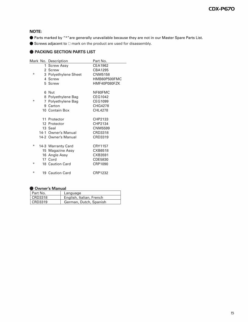
NOTE:
- Parts marked by “*”are generally unavailable because they are not in our Master Spare Parts List.
- Screws adjacent to ∇ mark on the product are used for disassembly.
1 Screw Assy CEA19622 Screw CBA1295
* 3 Polyethylene Sheet CNM51584 Screw HMB60P500FMC5 Screw HMF40P080FZK
6 Nut NF60FMC8 Polyethylene Bag CEG1042
* 7 Polyethylene Bag CEG10999 Carton CHG4278
10 Contain Box CHL4278
11 Protector CHP213312 Protector CHP213413 Seal CNM5599
14-1 Owner’s Manual CRD331814-2 Owner’s Manual CRD3319
* 14-3 Warranty Card CRY115715 Magazine Assy CXB651816 Angle Assy CXB359117 Cord CDE5830
* 18 Caution Card CRP1090
* 19 Caution Card CRP1232
- PACKING SECTION PARTS LIST
Mark No. Description Part No.
- Owner’s ManualPart No. LanguageCRD3318 English, Italian, FrenchCRD3319 German, Dutch, Spanish

6
CDX-P670
2.2 EXTERIOR
7
CDX-P670
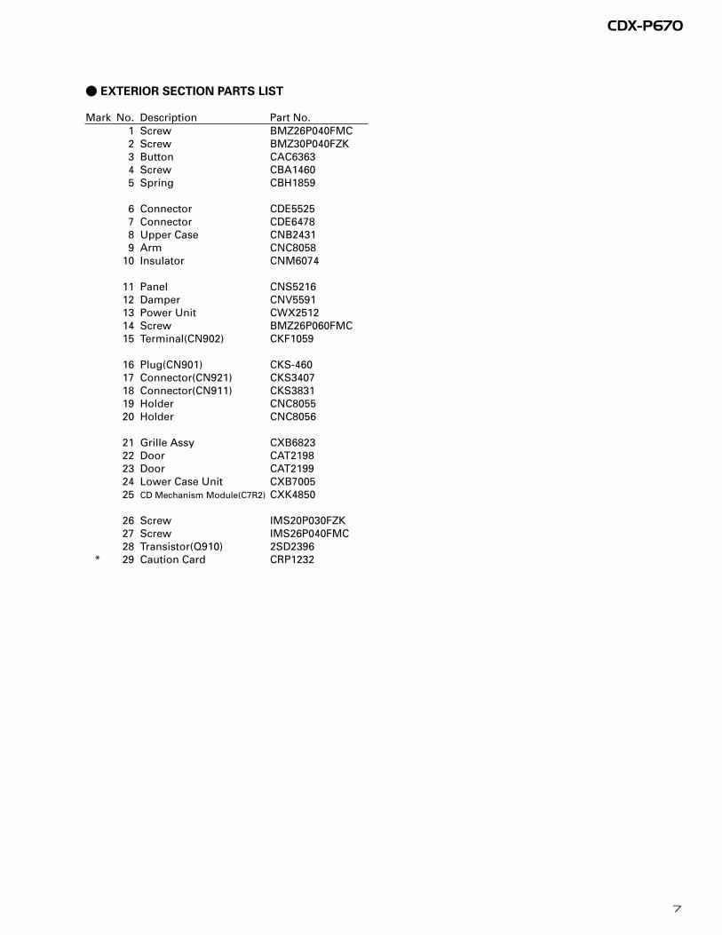
1 Screw BMZ26P040FMC2 Screw BMZ30P040FZK3 Button CAC63634 Screw CBA14605 Spring CBH1859
6 Connector CDE55257 Connector CDE64788 Upper Case CNB24319 Arm CNC8058
10 Insulator CNM6074
11 Panel CNS521612 Damper CNV559113 Power Unit CWX251214 Screw BMZ26P060FMC15 Terminal(CN902) CKF1059
16 Plug(CN901) CKS-46017 Connector(CN921) CKS340718 Connector(CN911) CKS383119 Holder CNC805520 Holder CNC8056
21 Grille Assy CXB682322 Door CAT219823 Door CAT219924 Lower Case Unit CXB700525 CD Mechanism Module(C7R2) CXK4850
26 Screw IMS20P030FZK27 Screw IMS26P040FMC28 Transistor(Q910) 2SD2396
* 29 Caution Card CRP1232
- EXTERIOR SECTION PARTS LIST
Mark No. Description Part No.

8
CDX-P670
2.3 CD MECHANISM MODULE
9
CDX-P670
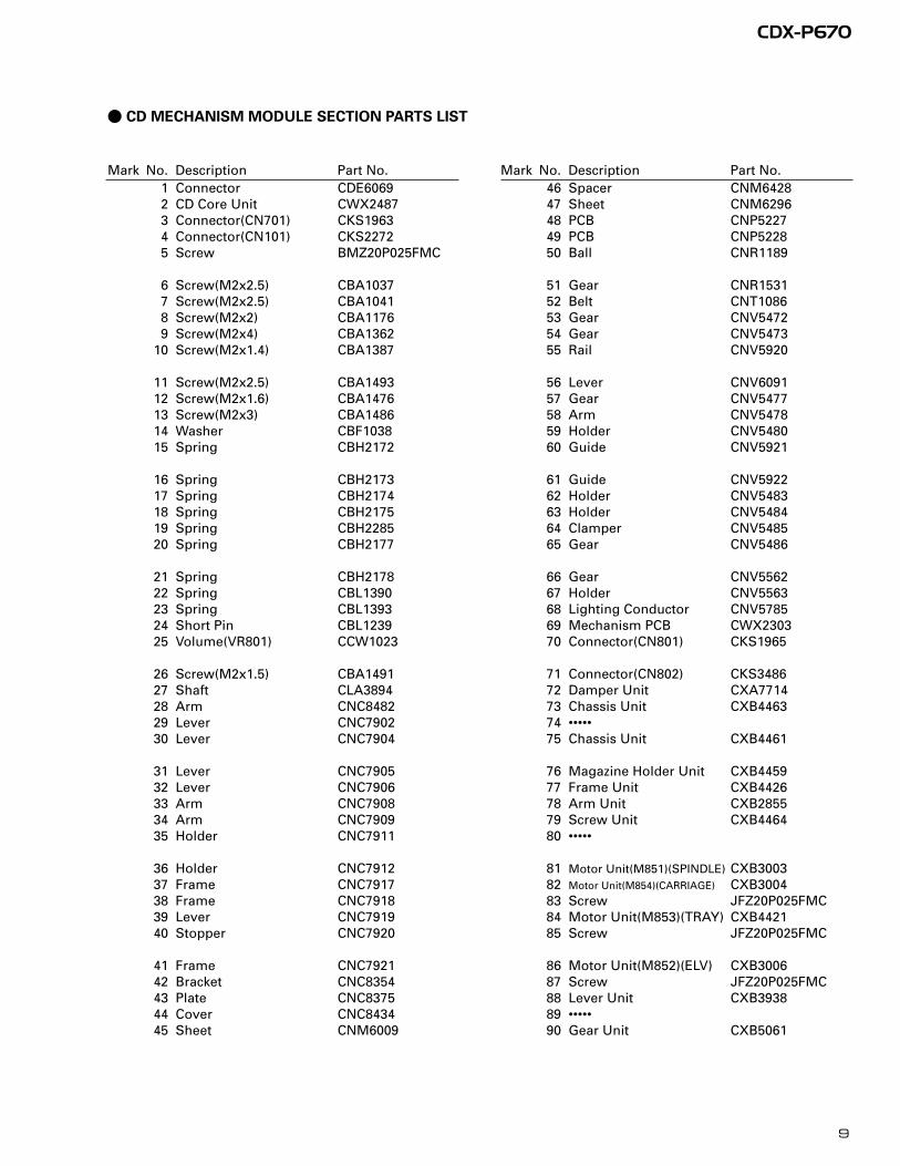
1 Connector CDE60692 CD Core Unit CWX24873 Connector(CN701) CKS19634 Connector(CN101) CKS22725 Screw BMZ20P025FMC
6 Screw(M2x2.5) CBA10377 Screw(M2x2.5) CBA10418 Screw(M2x2) CBA11769 Screw(M2x4) CBA1362
10 Screw(M2x1.4) CBA1387
11 Screw(M2x2.5) CBA149312 Screw(M2x1.6) CBA147613 Screw(M2x3) CBA148614 Washer CBF103815 Spring CBH2172
16 Spring CBH217317 Spring CBH217418 Spring CBH217519 Spring CBH228520 Spring CBH2177
21 Spring CBH217822 Spring CBL139023 Spring CBL139324 Short Pin CBL123925 Volume(VR801) CCW1023
26 Screw(M2x1.5) CBA149127 Shaft CLA389428 Arm CNC848229 Lever CNC790230 Lever CNC7904
31 Lever CNC790532 Lever CNC790633 Arm CNC790834 Arm CNC790935 Holder CNC7911
36 Holder CNC791237 Frame CNC791738 Frame CNC791839 Lever CNC791940 Stopper CNC7920
41 Frame CNC792142 Bracket CNC835443 Plate CNC837544 Cover CNC843445 Sheet CNM6009
46 Spacer CNM642847 Sheet CNM629648 PCB CNP522749 PCB CNP522850 Ball CNR1189
51 Gear CNR153152 Belt CNT108653 Gear CNV547254 Gear CNV547355 Rail CNV5920
56 Lever CNV609157 Gear CNV547758 Arm CNV547859 Holder CNV548060 Guide CNV5921
61 Guide CNV592262 Holder CNV548363 Holder CNV548464 Clamper CNV548565 Gear CNV5486
66 Gear CNV556267 Holder CNV556368 Lighting Conductor CNV578569 Mechanism PCB CWX230370 Connector(CN801) CKS1965
71 Connector(CN802) CKS348672 Damper Unit CXA771473 Chassis Unit CXB446374 •••••75 Chassis Unit CXB4461
76 Magazine Holder Unit CXB445977 Frame Unit CXB442678 Arm Unit CXB285579 Screw Unit CXB446480 •••••
81 Motor Unit(M851)(SPINDLE) CXB300382 Motor Unit(M854)(CARRIAGE) CXB300483 Screw JFZ20P025FMC84 Motor Unit(M853)(TRAY) CXB442185 Screw JFZ20P025FMC
86 Motor Unit(M852)(ELV) CXB300687 Screw JFZ20P025FMC88 Lever Unit CXB393889 •••••90 Gear Unit CXB5061
Mark No. Description Part No. Mark No. Description Part No.
- CD MECHANISM MODULE SECTION PARTS LIST
10
CDX-P670
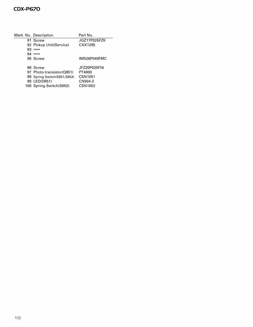
91 Screw JGZ17P025FZK92 Pickup Unit(Service) CXX128593 •••••94 •••••95 Screw IMS26P040FMC
96 Screw JFZ20P025FNI97 Photo-transistor(Q851) PT480098 Spring Switch(S851,S853) CSN105199 LED(D851) CN504-2
100 Spring Switch(S852) CSN1052
Mark No. Description Part No.

11
CDX-P670
2.4 MAGAZINE ASSY
1 Magazine Assy CXB65182 Label CRW14153 Tray CNV5341
- MAGAZINE ASSY SECTION PARTS LIST
Mark No. Description Part No.

PICKUP UNIT (SERVICE) (P8)
MECHANISMPCB
HOLOGRAMUNIT
FOCUS ACT.
TRACKING ACT.
FO+
149
98
39
AC/F/E/BD
FD/T
D/S
D/M
D
I13/I04/I02
97
1116151718
35
1012
DISC
TRP
DSP
DISCTRPDSP
929591
LD(–)
LASERDIODE
CARRIAGEMOTOR
MONITORDIODE MD
TO+
+5V
M
SPINDLEMOTOR
M
TRYMOTOR
HOME SW
TRPSW
DSPSW
VR802
EJECT SW
MAG SW
M
ELVMOTOR
M
17
12
27
1615
11
89
21
4
3
7
5
10
Q101
Q701
VD
PD
LIMITxtal
XTAL
L_OUT
LD
VREF
adena
cs
23
16
24IPIN
IPOUT
IPPW
POWER
XIN
XOUT 13
15
98
asens
bsens
reset
CDMUTE
ELV
RE
F
CONT
ELV
PV
O
ejsw
mag
disk
TRPDSP
11
94 93
74
75
3
X20216.93MHz
X70110.00MHz
IC 301BA5986FM
IC 302LB1836M
VDD
IC 701PD5638A
A CD CORE UNIT
Q851D851
D SWITCH PCB
E MOTOR PCB
C
S853
S801
S803
V
EVREF
GND
EPVO
L
4
3
7
5
11
89
21
10
17
12
27
1615
5
15
43
4CH SERVO DRIVER
MOTOR DRIVER
SYSTEMCONTROLLER
CN101CN
801
CN
802
S852
S851
RF AMP, SERVO, DSP, DAC
IC 201UPD63711GC
12
CDX-P6701 2 3 4
1 2 3 4
D
C
B
A
3. BLOCK DIAGRAM AND SCHEMATIC DIAGRAM
3.1 BLOCK DIAGRAM

8
1213
VD
5V
cs
IPINIPOUT
IPPW
POWER
484
2
1
2130
22
10
BUSP
15CDMUTE
LOUT
BUSM
asens
bsens
reset
9BATT+B
BSENINASENB
518 10
11
14
19 9
SVC2
56
12 7
4
3 1
RESET SW
5V REGULATOR
29
CDMUTE 76
8
56
20
ELV
PV
O
IC 202BA05FP
Q771
Q770
VDDIC 705
TC7SH32F
IC 702LC35256FT-70U
SRAM
IC 703HA12187FP
IP-BUS DRIVER
IC 704PAJ002A
CN701
16
B POWER UNIT
10 7
1
Q942
Q911
BUP
Q941
BUP
BUP
BUP
Q910
LOUT
3 CDMUTE
6 BP BUSP
LCH
5BUSM
8ASENB5 BM
7 ASNB
4 SVC
1
VD
POWER
VDVDVD
POWER
9 +B
13 BSENIN
CN911
IP-BUS OUT
CN921
L901BUP
GND
BATT.
GND
3
2
1
CN901FUSE
2A
10 8
2
17
16
Q912
S802
VR801
EPVO
LINEAR POSITION SENSOR
ER
1
2
3
CN902
13
CDX-P6705 6 7 8
5 6 7 8
D
C
B
A

14
CDX-P6701 2 3 4
1 2 3 4
D
C
B
A
1kΩ(B)
10kΩ(B)
1 12
6
13
10
4
8
VR801 CCW1023
LINEAR POSITION SENSOR
M852CXB3006
RF AMP, SE
MOTO
4CH SER
CN
801
CN
802
M853CXB4421
M851CXB3003
M854CXB3004
CSN1052
CSN1051
CSN1051
CN504-2 PT4800
PICKUP UNIT(SERVICE)CXX1285
CMECHANISM PCB
SWITCH PCBD
MOTOR PCBE
3.2 CD MECHANISM MODULE
Note: When ordering service parts, be sure to refer to “EXPLODED VIEWS AND PARTS LIST” or “ELECTRICAL PARTS
LIST”.
A1/2 C D E

15
CDX-P6705 6 7 8
5 6 7 8
D
C
B
A
18
7
2
5
19 20
15
17
16
21
3
9
1110
MP, SERVO, DSP, DAC
MOTOR DRIVER
H SERVO DRIVER
CD CORE UNITA
A2/2
Decimal points for resistorand capacitor fixed valuesare expressed as :2.2 2R20.022 R022
← ←
The > mark found on some component parts indicatesthe importance of the safety factor of the part.Therefore, when replacing, be sure to use parts ofidentical designation.
Symbol indicates a resistor.No differentiation is made between chip resistors anddiscrete resistors.
NOTE :
Symbol indicates a capacitor.No differentiation is made between chip capacitors anddiscrete capacitors.
A1/2

16
CDX-P6701 2 3 4
1 2 3 4
D
C
B
A
SYSTEM CONTROLLER
A1/2
A2/2

17
CDX-P6705 6 7 8
5 6 7 8
D
C
B
A
SRAM
IP-BUS DRIVER
BC
N91
1
A2/2

18
CDX-P670
1 RFI 0.5V/div. 0.5µs/div.Normal mode: play
1 CH1: RFI 1V/div.2 CH2: MIRR 5V/div.
Test mode: Tracking open
0.5ms/div. 1 CH1: RFI 1V/div.2 CH2: MIRR 5V/div.
Normal mode: The defect partpasses 800µm
0.5ms/div.
3 CH1: FD 0.5V/div.4 CH2: FOR 2V/div.
Test mode: No disc, Focus close
0.2s/div. 3 CH1: FD 0.5V/div.5 CH2: FOK 2V/div.
Normal mode: Focus close
0.2s/div. 6 CH1: FE 0.5V/div.7 CH2: XSI 2V/div.
Normal mode: Focus close
1ms/div.
REFO →
8 CH1: TE 0.5V/div.9 CH2: TD 0.5V/div.
Test mode: 32 tracks jump (REV)
0.5ms/div. 8 CH1: TE 0.5V/div.9 CH2: TD 0.5V/div.
Test mode: Single jump (REV)
0.5ms/div. 8 CH1: TE 0.5V/div.9 CH2: TD 0.5V/div.
Test mode: 100 tracks jump (REV)
5ms/div.
6 CH1: FE 0.1V/div.3 CH2: FD 0.2V/div.
Normal mode: Play
20ms/div. 3 CH1: FD 0.5V/div.0 CH2: MD 1V/div.
Normal mode: Focus close (12cm)
0.5s/div. 3 CH1: FD 0.5V/div.0 CH2: MD 1V/div.
Normal mode: Focus close (8cm)
0.5s/div.
REFO →
REFO →
REFO →
REFO →
REFO →
REFO →
GND →
REFO →
REFO →
REFO →
REFO →
REFO →
REFO →
REFO →
REFO →
REFO →
REFO →
REFO →
REFO →
- Waveforms
Note:1. The encircled numbers denote measuring pointes in the circuit diagram.2. Reference voltage
REFO:2.5V
REFO →
REFO →
REFO →
REFO →

19
CDX-P670
8 CH1: TE 0.2V/div.9 CH2: TD 0.2V/div.
Normal mode: play
8 CH1: TE 0.5V/div.! CH2: SD 0.5V/div.TEST mode:100Tracks jump(FWD)
5ms/div. 0 MD 0.5V/div. 0.1s/div.
Normal mode: Play (12cm)
0 MD 1V/div. 10ms/div.
Long Search (12cm)
@ EFM 1V/div. 5µs/div.
Normal mode: Play
8 CH1: TE 1V/div.# CH2: TEC 1V/div.
Test mode: Focus closeTracking open
2ms/div.
8 CH1: TE 0.5V/div.6 CH2: FE 0.5V/div.
Normal mode: AGC after focus close
0.2s/div.
20ms/div.
% SCKO 2V/div. 1µs/div.
Normal mode: Play
^ DOUT 2V/div. 10µs/div.
Normal mode: Play
& LRCK 2V/div. 20µs/div.Normal mode: Play
* VD 5V/div. 50ms/div.
Normal mode: No disc
GND →
REFO →
REFO →
GND →
REFO →
REFO →
REFO →
REFO →REFO →
REFO →
REFO →
REFO →
REFO →
GND →
REFO →
GND →
REFO →
GND →
REFO →

20
CDX-P670
( CH1: R OUT 2V/div.) CH2: L OUT 2V/div.
Normal mode: Play (1kHz 0dB)
6 CH1: FE 0.2V/div.3 CH2: FD 0.5V/div.
Normal mode: During AGC
1ms/div. 8 CH1: TE 0.2V/div.9 CH2: TD 0.5V/div.
Normal mode: During AGC
1 CH1: RFI 1V/div.⁄ CH2: HOLD 5V/div.
Normal mode: The defect part passes800µm(B.D)
500µs/div. 1ms/div.
0.5ms/div. 3 CH1: FD 1V/div.⁄ CH2: HOLD 5V/div.
Normal mode: The defect part passes800µm(B.D)
0.5ms/div.9 CH1: TD 0.1V/div.⁄ CH2: HOLD 5V/div.
Normal mode: The defect part passes800µm(B.D)
0.5ms/div.
REFO →
REFO →
REFO →
REFO →
REFO →
REFO →
REFO →
REFO → REFO →
REFO →
REFO →
REFO →

8V R
EG
.
MU
TE
CN701
BP
OW
ER
UN
IT
A2/2
3.3 POWER UNIT CEK1033
21
CDX-P6701 2 3 4
1 2 3 4
D
C
B
A
B

22
CDX-P6701 2 3 4
1 2 3 4
D
C
B
A
CapacitorConnector
P.C.Board Chip Part
SIDE A
SIDE B
2. Viewpoint of PCB diagrams
SIDE A
CD
CO
RE
UN
ITA
4. PCB CONNECTION DIAGRAM
4.1 CD CORE UNIT
NOTE FOR PCB DIAGRAMS
1. The parts mounted on this PCB
include all necessary parts for
several destination.
For further information for
respective destinations, be sure
to check with the schematic dia-
gram.
E
E
IC, Q
AD
J
M
M852ELV
BC
N91
1
CC
N80
1
E
FR
EFO
ER
EF
EP
VO
125
26 5051
757610
0
A

23
CDX-P6701 2 3 4
1 2 3 4
D
C
B
A
E
E
E
IC, Q
RE
SE
TE
JEC
T
MA
G
SIDE B
CD
CO
RE
UN
ITA
A
24
CDX-P6701 2 3 4
1 2 3 4
D
C
B
A
B
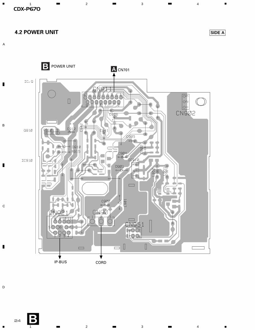
SIDE A4.2 POWER UNIT
A CN701
IP-BUS
POWER UNITB
CORD
25
CDX-P6701 2 3 4
1 2 3 4
D
C
B
A
B
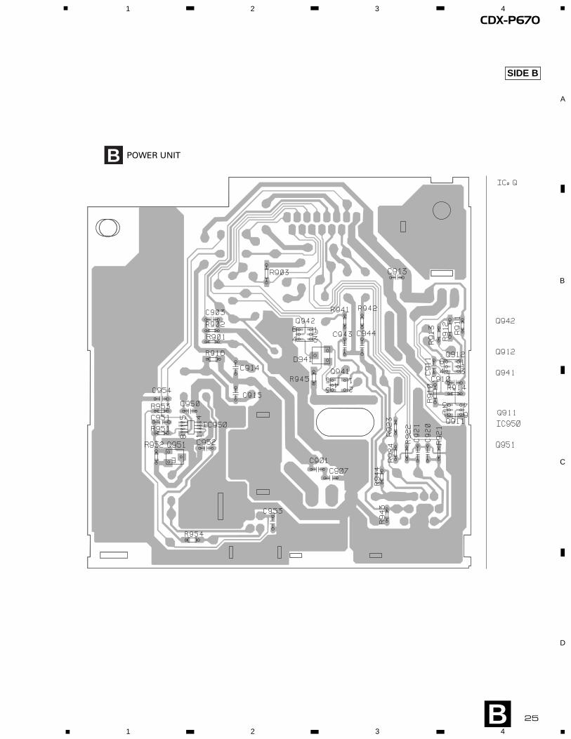
SIDE B
POWER UNITB
26
CDX-P6701 2 3 4
1 2 3 4
D
C
B
A
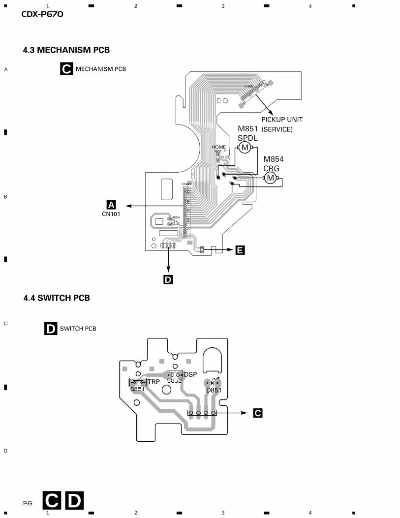
4.4 SWITCH PCB
SWITCH PCBD
C
4.3 MECHANISM PCB
ACN101
E
D
MECHANISM PCBC
M
M854CRG
M
M851SPDL
HOME
TRPDSP
D851
PICKUP UNIT
(SERVICE)
C D
27
CDX-P6701 2 3 4
1 2 3 4
D
C
B
A
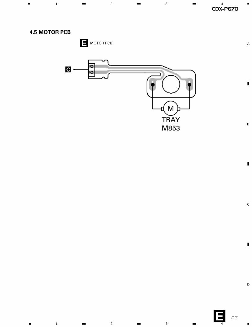
4.5 MOTOR PCB
MOTOR PCBE
E
C

28
CDX-P670
Unit Number : CWX2487Unit Name : CD Core Unit
MISCELLANEOUS
IC 201 IC UPD63711GCIC 202 IC BA05FPIC 301 IC BA5986FMIC 302 IC LB1836MIC 701 IC PD5638A
IC 702 IC LC35256FT-70UIC 703 IC HA12187FPIC 704 IC PAJ002AIC 705 IC TC7SH32FQ 101 Transistor 2SB1132
Q 701 Transistor DTA144EKQ 770 Transistor 2SB1184F5Q 771 Transistor 2SC2412KD 730 Diode 1SS356D 770 Diode 1SS355
X 202 Ceramic Resonator 16.93MHz CSS1536X 701 Radiator 10.00MHz CSS1428S 801 Push Switch(EJECT) CSG1139S 802 Push Switch(RESET) CSG1139S 803 Spring Switch(MAG) CSN1044
VR 802 Semi-fixed 1kΩ(B) CCP1338
RESISTORS
R 101 RS1/8S120JR 102 RS1/8S100JR 103 RS1/16S222JR 201 RS1/16S104JR 202 RS1/16S0R0J
R 205 RS1/16S103JR 206 RS1/16S393JR 207 RS1/16S182JR 213 RS1/16S103JR 214 RS1/16S103J
R 215 RS1/16S123JR 231 RS1/16S821JR 232 RS1/16S821JR 253 RS1/16S681JR 254 RS1/16S681J
R 256 RS1/16S681JR 257 RS1/16S681JR 258 RS1/16S681JR 259 RS1/16S102JR 260 RS1/16S681J
R 298 RS1/16S681JR 301 RS1/16S103JR 302 RS1/16S153JR 303 RS1/16S103JR 304 RS1/16S103J
R 305 RS1/16S103JR 306 RS1/16S752JR 307 RS1/16S103JR 308 RS1/16S752JR 309 RAB4C332J
R 311 RS1/16S102JR 701 RS1/16S681JR 702 RS1/16S102JR 703 RS1/16S222JR 704 RS1/16S104J
R 705 RS1/16S104JR 706 RS1/16S222JR 707 RS1/16S104JR 708 RS1/16S0R0JR 715 RS1/16S473J
R 716 RS1/16S103JR 717 RS1/16S473JR 718 RS1/16S681JR 719 RS1/16S0R0JR 721 RS1/16S222J
R 722 RS1/16S222JR 724 RS1/16S681JR 725 RS1/16S222JR 726 RS1/16S104JR 727 RS1/16S513J
R 729 RS1/16S473JR 730 RS1/16S473JR 731 RS1/16S222JR 732 RS1/16S683JR 733 RS1/16S222J
R 734 RS1/16S473JR 735 RS1/16S222JR 736 RS1/16S103JR 737 RS1/16S433JR 738 RS1/16S104J
R 739 RS1/8S1R0JR 740 RS1/8S2R0JR 741 RS1/16S102JR 742 RS1/16S104JR 743 RS1/16S104J
R 744 RS1/16S223JR 745 RS1/16S104JR 747 RS1/16S472JR 750 RAB4C473JR 751 RAB4C473J
R 752 RS1/16S3602DR 753 RS1/16S6801DR 754 RS1/16S221JR 755 RS1/16S104JR 756 RS1/16S221J
R 759 RS1/16S472JR 760 RS1/16S104JR 761 RS1/16S104JR 764 RS1/16S473JR 768 RS1/8S220J
5. ELECTRICAL PARTS LIST
NOTE:
- Parts whose parts numbers are omitted are subject to being not supplied.
- The part numbers shown below indicate chip components.
Chip Resistor
RS1/_S___J,RS1/__S___J
Chip Capacitor (except for CQS.....)
CKS....., CCS....., CSZS.....
=====Circuit Symbol and No.===Part Name Part No.--- ------ ------------------------------------------ -------------------------
=====Circuit Symbol and No.===Part Name Part No.--- ------ ------------------------------------------ -------------------------
A

29
CDX-P670
R 801 RS1/10S221JR 802 RS1/10S271JR 804 RS1/16S562JR 805 RS1/16S562JR 806 RS1/16S102J
CAPACITORS
C 101 CKSRYB102K50C 102 CKSRYB104K16C 103 CEV101M6R3C 104 CEV470M6R3C 105 CKSRYB224K16
C 106 CKSRYB224K16C 107 CKSRYB224K16C 201 CKSRYB104K16C 202 CEV101M6R3C 203 CKSRYB104K16
C 204 CKSRYB332K50C 205 CKSRYB104K16C 206 CKSRYB392K50C 207 CKSRYB104K16C 208 CCSRCH270J50
C 209 CCSRCJ3R0C50C 210 CCSRCH181J50C 211 CCSRCH510J50C 212 CKSRYB682K50C 213 CKSRYB104K16
C 214 CKSRYB104K16C 215 CKSRYB104K16C 216 CKSRYB104K16C 217 CKSRYB104K16C 218 CKSRYB104K16
C 219 CKSQYB334K16C 220 CKSRYB104K16C 234 CKSRYB224K16C 235 CEV220M6R3C 236 CCSQSL152J50
C 237 CCSQSL152J50C 238 CKSRYB103K25C 253 CKSRYB471K50C 271 CEV101M6R3C 272 10µF/16V CCH1399
C 273 CKSRYB224K16C 301 CEV101M10C 302 CKSRYB224K16C 701 CKSRYB104K16C 702 CKSRYB473K16
C 703 CKSRYB473K16C 707 CKSRYB103K25C 708 CKSRYB104K16C 710 CKSRYB103K25C 711 CKSRYB102K50
C 712 CKSRYB102K50C 714 CKSRYB104K16C 715 22µF/10V CCH1403C 717 CKSRYB103K25C 718 CKSRYB103K25
C 719 CKSRYB102K50C 720 CKSRYB102K50C 721 CKSRYB103K25C 722 CKSRYB103K25C 724 CKSRYB471K50
C 801 CKSRYB103K25C 802 CKSRYB104K16C 803 CKSRYB103K25
Unit Number : CWX2512Unit Name : Power Unit
MISCELLANEOUS
Q 910 Transistor 2SD2396Q 911 Transistor IMD2AQ 912 Transistor IMX1Q 941 Transistor FMG12Q 942 Transistor IMD2A
D 901 Diode 1SR139-400D 902 Diode 1SR139-400D 910 Diode HZS6L(B1)D 941 Diode MA152WAL 901 Choke Coil 1mH CTH1047
RESISTORS
R 901 RS1/16S204JR 902 RS1/16S104JR 903 RS1/4SA101JR 910 RS1/8S431JR 911 RS1/16S681J
R 912 RS1/8S101JR 913 RS1/16S512JR 914 RS1/16S132JR 915 RD1/4PU151JR 921 RS1/16S101J
R 922 RS1/16S101JR 923 RS1/16S102JR 924 RS1/16S473JR 941 RS1/16S181JR 942 RS1/16S181J
R 943 RS1/16S472JR 944 RS1/16S472JR 945 RS1/10S472J
CAPACITORS
C 901 CKSRYB224K16C 902 CEAT471M16C 903 CKSRYB223K25C 904 CEAT471M16C 906 0.1F/5.5V CCL1054
C 907 CKSRYB224K16C 910 CKSRYB103K50C 911 CKSRYB103K50C 912 CEJA220M10C 913 CKSRYB103K50
C 920 CCSRCH471J50C 921 CCSRCH471J50C 941 CEJA330M10C 942 CEJA330M10C 943 CCSRCH471J50
C 944 CCSRCH471J50
Unit Number :Unit Name : Mechanism PCB
Q 851 Photo-transistor PT4800S 853 Spring Switch(HOME) CSN1051
Unit Number :Unit Name : Switch PCB
D 851 LED CN504-2S 851 Spring Switch(TAP) CSN1051S 852 Spring Switch(DSP) CSN1052
=====Circuit Symbol and No.===Part Name Part No.--- ------ ------------------------------------------ -------------------------
=====Circuit Symbol and No.===Part Name Part No.--- ------ ------------------------------------------ -------------------------
B
C
D

30
CDX-P670
Unit Number :Unit Name : Motor PCB
M 853 Motor Unit(TRAY) CXB4421
Miscellaneous Parts List
Pickup Unit(P8)(Service) CXX1285M 851 Motor Unit(SPINDLE) CXB3003M 852 Motor Unit(ELV) CXB3006M 854 Motor Unit(CARRIAGE) CXB3004VR 801 Volume 10kΩ(B) CCW1023
=====Circuit Symbol and No.===Part Name Part No.--- ------ ------------------------------------------ -------------------------
E

31
CDX-P670
- Precautions• This unit uses a single power supply (+5V) for the reg-
ulator. The signal reference potential, therefore, isconnected to REFO(approx. 2.5V) instead of GND.If REFO and GND are connected to each other by mis-take during adjustments, not only will it be impossi-ble to measure the potential correctly, but the servowill malfunction and a severe shock will be applied tothe pick-up. To avoid this, take special note of the fol-lowing.Do not connect the negative probe of the measuringequipment to REFO and GND together. It is especiallyimportant not to connect the channel 1 negativeprobe of the oscilloscope to REFO with the channel 2negative probe connected to GND.Since the frame of the measuring instrument is usual-ly at the same potential as the negative probe, changethe frame of the measuring instrument to floating sta-tus.If by accident REFO comes in contact with GND,immediately switch the regulator or power OFF.
• Always make sure the regulator is OFF when connect-ing and disconnecting the various filters and wiringrequired for measurements.
• Before proceeding to further adjustments and mea-surements after switching regulator ON, let the playerrun for about one minute to allow the circuits to stabi-lize.
• Since the protective systems in the unit's software arerendered inoperative in test mode, be very careful toavoid mechanical and /or electrical shocks to the sys-tem when making adjustment.
• Disc detection during tray extraction and return oper-ations is performed by means of the photo transistorin this unit. Consequently, if the inside of the unit isexposed to a strong light source with the outer casingremoved for repairs or adjustment, the following mal-functions may occur:
*Even with a disc loaded, the unit detects "no disc"and cannot start play.
*Although a 12-cm disc is loaded, the unit detects"8cm disc" mistakenly.
When the unit malfunctions this way, either re-posi-tion the light source, move the unit or cover the phototransistor.
• During exchanging discs, do not press the keys forthe discs to be exchanged.
Key to adjustment text HEAD UNIT (6 keys type)
inside (12 keys type)
BAND BAND
TRK+/FF TRK+/FF
TRK-/REV TRK-/REV
7 1
8 2
9 3
10 4
11 5
12 6
DISC- DISC-
SOURCE ON/OFF SOURCE ON/OFF
6. ADJUSTMENT
6.1 CD ADJUSTMENT

32
CDX-P670
• Note :CD mechanism modules the grating angle of the pickup unit cannot be adjusted after the pickup unit is changed.The pickup unit in the CD mechanism module is adjusted on the production line to match the CD mechanismmodule and is thus the best adjusted pickup unit for the CD mechanism module. Changing the pickup unit is thusbest considered as a last resort. However, if the pickup unit must be changed, the grating should be checkedusing the procedure below.
• Purpose :To check that the grating is within an acceptable range.
• Symptoms of Mal-adjustment :If the grating is off by a large amount symptoms such as being unable to close tracking, being unable to performtrack search operations, or track searching taking a long time, may appear.
• Method :
• Measuring Equipment • Oscilloscope, Two L.P.F.• Measuring Points • E, F, REFO• Disc • ABEX TCD-784• Mode • TEST MODE
• Checking Procedure1. Enter Test mode, then select Multi-CD player and switch the 5V regulator on.2. Using the TRK+ and TRK- buttons, move the pickup unit to the innermost track.3. Press key 9 to close focus, the display should read "91". Press key 9 2 times. Enter Rough Servo mode. Press key
8 to implement the tracking balance adjustment the display should now read "81".4. As shown in the diagram above, monitor the LPF outputs using the oscilloscope and check that the phase differ-
ence is within 75° . Refer to the photographs supplied to determine the phase angle.5. If the phase difference is determined to be greater than 75° try changing the pickup unit to see if there is any
improvement. If, after trying this a number of times, the grating angle does not become less than 75° then themechanism should be judged to be at fault.
• NoteBecause of eccentricity in the disc and a slight misalignment of the clamping center the grating waveform may beseen to "wobble" ( the phase difference changes as the disc rotates). The angle specified above indicates the aver-age angle.
• HintChange the disc changes the clamp position and may decrease the "wobble".
REFO
E
F
E
F
L.P.F.
L.P.F.
CD CORE UNIT
Xch Ych
Oscilloscope100kΩ
100kΩ
390pF
390pF
6.2 CHECKING THE GRATING
- Checking the Grating After Changing the Pickup Unit

33
CDX-P670
Grating waveform
45˚
0˚
75˚
60˚
30˚
90˚
Echt Xch 20mV/div, ACFcht Ych 20mV/div, AC

34
CDX-P670
• Note :This mechanisms is detects the height of the stage using slide-variable resistance.To absorb dislocation of the stage height caused by differences in the mechanism and the CD core unit, adjustmentmust be made for each CD-mechanism module using a variable resistor.Normally, readjustment is not needed, as this has been adjusted at the factory. However, adjustment of elevation isrequired according to the procedure explained below if an elevation error has occurred or if the CD core unit hasbeen removed.
• Purpose :To adjust and confirm whether or not elevation operates correctly.
• Adjustment Method :
• Measuring Equlpment: Oscilloscope, One L.P.F.• Measuring Points : EREF, EPVO• Setting : Without a magazine in Test mode
With the mechanism placed upside-down (Place the CD mechanism module so that the CDcore unit is above.)
• Confirmation Procedure
1. Enter Test mode, then select Multi-CD player.
2. Press key 7 to enter Mechanism Test mode.
3. Press key 12 twice to specify the amount of movement.
6.3 ADJUSTMENT OF ELEVATION WHEN THE CD CORE UNIT HAS BEEN REMOVED
FOR MAINTENANCE- Adjustment When Error Code 60 is Displayed Because of Malfunctioning Elevation
TRACK FUNCTION
' "
TRACK FUNCTION
72 00' 00"
EREF
EPVO
Oscilloscope
CD CORE UNIT
L.P.F.
47kΩ1µF
Examples of display
TRACK FUNCTION
72 00' 02"
TRACK FUNCTION
72 00' 01"
The amount of movementchanges each time key 12 ispressed.
maximum movementi
Key 12i
during movementi
Key 12i
minimum movementTRACK FUNCTION
72 00' 00"i
i
Key 12

35
CDX-P670
4. Press key 9 to set ELV/TRAY mode to TRAY.
5. Press key FF to release the clamp and return the tray to the magazine.
6. Press key 9 to enter Elevation Move mode.
7. Use key FF/REV to operate elevation and set if to the graduation of the third step(Fig. 1).
8. Make the adjustment. Use VR802 to adjust the difference in potential between EREF and EPVO to 0 ±10mV.
9. When adjustment is completed, press key BAND to exit Mechanism Test mode.
10. Confirm operation of the mechanism.Place the mechanism horizontally (CD core unit below). Take care not to short-cir-cuit the PCB.
11. Confirm the height of the stage. Use the DISC± key to select Disc No.3.
Check if the stopper bend of the clamp lever is engaged in the groove of the framestopper (Fig. 2-4).
• Note :The stopper bend will be pressed downward into the groove for final clamping. Confirm the engagement positionof the stopper bend.
• If the stopper bend is engaged in the center and pressed downward, adjustment is completed. Go to step 15.
• If the stopper bend is dislocated, check the amount of dislocation by following steps 12 to 14.
TRACK FUNCTION
72 00' 02"
TRACK FUNCTION
72 00' 02"
TRACK FUNCTION
' "
TRACK FUNCTION
04 00' 00"
Examples of display
TRACK FUNCTION
72 01' 02"
Release the clamp

36
CDX-P670
12. To see the amount of dislocation, place the mechanism upside-down.If the stopper bend has been dislocated in the direction of the firstCD, turn VR802 to the left(Fig. 2).
To lower the stage toward the sixth step by 0.1 mm, reduce the volt-age of EREF (adjusted in step 8) by 20 mV.
If the stopper bend has been dislocated in the direction of the sixthCD, turn VR802 to the right(Fig. 4).
To raise the stage toward the first step by 0.1 mm, increase the volt-age of EREF (adjusted in step 8) by 20 mV.
13. Place the mechanism horizontal. Go back to step 11 to reconfirm thestage height.
14. When adjustment of the stage height is completed, proceed as fol-lows:
15. Press the EJECT switch.
16. Once operation of the mechanism has stopped, turn the power OFF.
17. Wait more than one minute after the power is turned off, then turn the power ON and insert a magazine.
18. Check if the mechanism operates correctly with the first and fourth CDs.
19. If the mechanism operates properly, adjustment is completed. If the mechanism operates improperly, make theadjustment again.
GNDEREF
VR802
1µF
47kΩ
Oscilloscope
L.P.F.

37
CDX-P670
NG
Stopper bend of theclamp lever
Frame stopper
OK
Engaged in the center and pressed downward.
NG
Fig. 1
Dislocated toward the first CD.
Adjust the insertion gate of magazine tothe third scale.
E12346
Dislocated toward the sixth CD.
Fig. 2
Fig. 3
Fig. 4

38
CDX-P670
7. GENERAL INFORMATION
7.1 DIAGNOSIS
7.1.1 TEST MODE
- CD Test mode
This mode is used for adjusting the CD mechanism
module of the device.
• Test mode starting procedureReset while pressing the 4 and 6 keys together.
• Test mode cancellationSwitch ACC, back-up OFF.
• If the 8 or 9 key is pressed while focus search is inprogress, immediately turn the power off (otherwisethe actuator may be damaged due to the lens stuck).
• Jump operation of TRs other than 100TR continuesafter releasing the key. CRG move and 100TR jumpoperations are brought into the “Tracking close” sta-tus when the key is released.
• Powering Off/On resets the jump mode to “Single TR(91)”, the RF AMP gain setting to 0 dB, and the auto-matic adjustment value to the initial value.
• During exchanging discs, do not press the keys forthe discs to be exchanged.
• The following head units are exceptional so that theirentering ways to the test mode are different from oth-ers.Test mode starting procedureReset while pressing the 3 and 5 keys together.
KEH-P5010R/X1M/EW
KEH-4011/X1M/EE
KEH-P5011/X1M/EE
KEH-4010R/X1M/EW
KEH-P4010RB/X1M/EW
KEH-P4013R/X1M/EW
KEH-5015/X1M/ES
KEH-P4010/X1M/UC
KEH-P4015/X1M/ES

39
CDX-P670
Focus Close*2 S Curve Check01 01 0100 00 00
(99 99 99)Display
TYP
4
9
Reset
SOURCE
New test mode
6
TRK-
BAND
9
*2
*1 +6dB +12dB
*4
*5
12
12
12
12
7
8
7
8TRK+
TRK+ TRK-
06 06 06 12 12 12
Sourse CD
Single TR 9x(8x):91(81)
32TRK92(82)
CRG Move94(84)
100TRK93(83)
Focus ModeSelect
Focus Close/S Curve Check
CRG− Auto AdjustmentDisplay Select
<Tracking Servo Close> CRG+
RF AGC Coefficient Display/Rough Servo and RF AGC
Tracking Open
Display
TrackingOpen
T. Close andFit Servo
*3 F.Offset Display RF.Offset Display F.Cansel Display
*7
Single TR/32TR/100TR
Voltage of CRG Motor = 2 [V]
(F,T.AGC Gain = (Present Value/Initial Value) × 20)
*6
TRK+ TRK-
7
9
Display
8
9
Displayor
8x 8x 8xTRK SECMIN
9x 9x 9xTRK SECMIN
or
CRG−CRG+ T.BalanceAdjustment
*7F, T, RF AGC/F.Bias Display Select
F, T AGC andRF AGC
CRG Move, 100TR Jump Only
TRK, MIN, SEC F.AGC Gain RF AGC GainT.AGC Gain
*8
Power ON(Adjustment for T.Offset)
*5 *4 *4
*6CRG/TR Jump NO.Select
CRG+/TR Jump+CRG−/TR Jump−
Power OFF
Display
Display
Display
T.Close andF,T AGC andRF AGC andFit Servo
Display
Power ON(Not adjustment for T.Offset)
Display
Display
8
RF AMP Gain Select
8
Power OFF
Power OFF
Power OFF 8x 8x 8xTRK SECMIN
9x 9x 9xTRK SECMIN
8x 8x 8xTRK SECMIN
9x 9x 9xTRK SECMIN
or
8x 8x 8xTRK SECMIN
9x 9x 9xTRK SECMIN
or
00 00 00TRK SECMIN
99 99 99TRK SECMIN
or
00 00 00TRK SECMIN
99 99 99TRK SECMIN
or
00 00 00TRK SECMIN
99 99 99TRK SECMIN
or
91 91 91TRK SECMIN
0x 0x 0xTRK SECMIN
00 00 00TRK SECMIN
99 99 99TRK SECMIN
GG GG GGTRK SECMIN
Test Mode In
*1
*8 *3*8
F.Cancel Value = Top Rank 8bit of Set Value (7F [H] to 80 [H] ) + 128 / 4 = 63 [D] to (32 [D] ) to 00 [D]
BAND
BAND
BAND
BAND
9 12 FF
7
REV BAND
Display
< Mechanism test mode in > Display
<ELV,TRAY select> <Operation mode select >
<Shift > <Shift >
*9 *12*11*10
<Mechanism test mode out >
72 00 00TRK SECMIN
TRK SECMIN
0X0072
*9 ELV motor select
*10
Display
TRAY motor select
0X1072
000072 010072 020072
8ms pulse drive
Display
24ms pulse drive DC drive
*11
001072 011072 021072
48ms pulse drive
Display
100ms pulse drive DC drive
ELV select : ELV dowm (Disc 12 → 1)TRAY select : TRAY out
*12 ELV select : ELV up (Disc 1 → 12)TRAY select : TRAY in
- Flow Chart

40
CDX-P670
- Error Messages
If a CD is not operative or stopped during operation due to an error, the error mode is turned on and cause(s) of the
error is indicated with a corresponding number. This arrangement is intended at reducing nonsense calls from the
users and also for facilitating trouble analysis and repair work in servicing.
(1) Basic Indication Method
1) When SERRORM is selected for the CSMOD (CD mode area for the system), error codes are written to DMIN (min-
utes display area) and DSEC (seconds display area). The same data is written to DMIN and DSEC. DTNO remains
in blank as before.
2) Head unit display examples
Depending on display capability of LCD used, display will vary as shown below. xx contains the error number.
8-digit display 6-digit display 4-digit display
ERROR–xx ERR–xx E–xx
OR
Err–xx
* When the system is manufactured for an OEM basis, the error display will be configured according to the customer
specification.
(2) Error Code List
Code Class Displayed error code Description of the code and potential cause(s)
10 Electricity Carriage Home NG CRG can't be moved to inner diameter.
CRG can't be moved from inner diameter.
→ Failure on home switch or CRG move mechanism.
11 Electricity Focus Servo NG Focusing not available.
→ Stains on rear side of disc or excessive vibrations on REWRITABLE.
12 Electricity Spindle Lock NG Spindle not locked. Sub-code is strange (not readable).
→ Failure on spindle, stains or damages on disc, or excessive vibrations.
Subcode NG A disc not containing CD-R data is found. Turned over disc are found,
though rarely.
→ Failure on home switch or CRG move mechanism.
RF AMP NG An appropriate RF AMP gain can't be determined.
→ CD signal error.
17 Electricity Setup NG APC protection doesn't work. Focus can be easily lost.
→ Damages or stains on disc, or excessive vibrations.
30 Electricity Search Time Out Failed to reach target address.
→ CRG tracking error or damages on disc.
A0 System Power Supply NG Power (VD) is ground faulted.
→ Failure on SW transistor or power supply (failure on connector).
A1 System Mechanism power Mechanism elevation reference voltage is out of
failure prescription.
→EREF adjustment VR and/or power abnormal.
50 Mecha- An error upon MAG switch release time has time out.
nism ejection Elevation time out when eject.
60 Mecha- An error while putti- Tray in / out time has time out.
nism ng in and out the tray Tray is caught when put in.

41
CDX-P670
Code Class Displayed error code Description of the code and potential cause(s)
70 Mecha- An error upon Elevation time has time out.
nism elevation
80 Mecha- An error with an em- No disc is available.
nism pty magazine inserted
Remarks: Unreadable TOC does not constitute an error. An intended operation continues in this case.
A newly designed head unit must conform to the example given above.
Upper digits of an error code are subdivided as shown below:
1x: Setup relevant errors, 3x: Search relevant errors, 3x: Search relevant errors, Ax: Other errors.
- New Test Mode
M-CD plays the same way as before.
If an error such as off focus, spindle unlocking, unreadable sub-code, or sound skipping occurs after setup, its
cause and time occurred (in absolute time) are displayed.
During setup, operational status of the control software (internal RAM: CPOINT) is displayed.
These displays and functions are prepared for enhancing aging in the servicing and efficiency of trouble analysis.
(1) Shifting to the New Test Mode
1 Turn on the current test mode by starting the reset from the 4 and 6 keys together.
2 Select M-CD for the source through the specified procedure including use of the [SOURCE] key. Then, press the
12 key while maintaining the regulator turned off.
3 After the above operations, the new test mode remains on irrespective of whether the M-CD is turned on or off.
You can reset the new test mode by turning on the reset start.
* With some products, the new test mode can be reset through the same operations as that employed for shifting to
the STBY mode (while maintaining the Acc turned off).
(2) Key Correspondence
Key Test mode New test mode
(Example) Power Off Power On In-play Error Production
BAND To power on To power off – Time/Err.No. switching
(offset adjustment performed)
UP – FWD-Kick FF/TR+ –
DOWN – REV-Kick REV/TR- –
7 – T.Close (AGC performed) Scan –
/parameter display switching
8 RF AMP gain switching Parameter display switching Mode –
/T.BAL adjustment/T.Open
9 To power on F.Close/RF AGC/F.T.AGC – –
(offset adjustment not performed)
10 – F.Open – –
11 – Jump Off – –
12 – F.Mode switching Auto/Manu T.No./Time switching
/T.Close (no AGC)/Jump switching

42
CDX-P670
Key Mechanism Test Mode
(Example)
BAND Back to the test mode
UP Playing the mechanism
DOWN Playing the mechanism
7 Mechanism test mode in
8 –
9 TRAY/ELV select
10 –
11 –
12 Operation step select
Note: Eject and CD on/off is performed in the same procedure as that for the normal mode.
(3) Cause of Error and Error Code
Code Class Contents Description and cause
40 Electricity Off focus detected. FOK goes low.
→ Damages/stains on disc, vibrations or failure on servo.
41 Electricity Spindle unlocked. FOK = Low continued for 50 msec.
→ Damages/stains on disc, vibrations or failure on servo.
42 Electricity Sub-code unreadable. Sub-code was unreadable for 50 msec.
→ Damages/stains on disc, vibrations or failure on servo.
43 Electricity Sound skipping detected. Last address memory function was activated.
→ Damages/stains on disc, vibrations or failure on servo.
Note: Mechanical errors during aging are not displayed.
The error codes should be indicated in the same way as in the normal mode.
(4) Display of Operational Status (CPOINT) during SetupStatus No. Contents Protective action00 CD+5V ON process in progress. None01 Servo LSI initialization (1/3) in progress. None02 Servo LSI CRAM initialization in progress. None03 Servo LSI initialization (2/3) in progress. None04 Offset adjustment (1/3) in progress. None05 Offset adjustment (2/3) in progress. None06 Offset adjustment (3/3) in progress. None07 FZD adjustment in progress. None08 Servo LSI initialization (3/3) in progress. None10 Carriage move to home position started. None11 Carriage move to home position started. None12 Carriage is moving toward inner diameter. Specified 10 seconds has been passed or failure
on home switch.13 Carriage is moving toward outer diameter. Specified 10 seconds has been passed or failure
on home switch.14 Carriage outer kick in progress. None15 Carriage outer diameter feed (1 second) in progress. None20 Servo close started. None21 Pre-processing for focus search started. None22 Spindle rotation and focus search started. None23 Waiting for focus close (XSI=Low). Specified focus search time has been passed.24 Standing by after focus close is over. Specified focus search time has been passed.25 Focus search preprocessing is in None
progress while setup protection is turned on.

43
CDX-P670
Status No. Contents Protective action26 Focus search preprocessing is in None
progress while focus recovery is turned on.27 Wait time after focus close is set up. Off focus.28 Standing by after focus close is over. Off focus.29 Setup (1/2) before T balance adjustment is started. Off focus.30 Setup (2/2) before T balance adjustment is started. Off focus.31 T balance adjustment started. Off focus.32 T balance adjustment (1/2). Off focus.33 T balance adjustment (2/2). Off focus.34 Waiting for spindle rotation to end. Off focus.
Spindle rough servo.35 Standing by after spindle rough servo is over. Off focus.36 RF AGC started. Off focus.37 RF AGC started. Off focus.38 RF AGC ending process in progress. Off focus.39 Tracking close in progress. Off focus.40 Standing by after tracking is closed. Off focus.
Carriage closing in progress.41 Focus/tracking AGC started. Off focus.42 Focus AGC started. Off focus.43 Focus AGC in progress. Off focus.44 Tracking AGC in progress. Off focus.45 Standing by after focus/tracking AGC are over. Off focus.46 Spindle processes applicable servo. Off focus.47 Check for servo close is started. Off focus.48 Check of LOCK pin started. Off focus or spindle not locked.49 RF AGC started. Off focus.50 RF AGC in progress. Off focus.51 Standing by after RF AGC is over. Off focus.
(5) Display Examples
1) During Setup (When status no. = 11)
TRK No. MIN. SEC.
11 11' 11"
2) During Operation (TOC read, TRK search, Play, FF and REV)
The same as in the normal mode.
3) When a Protection Error Occurred
Switch to the following displays (A) and (B) using the [BAND] switch:
(A) Error occurrence timing display in absolute time.
An example: Error occurred in 12th tune at 34'56" in absolute time.
TRK No. MIN. SEC.
12 34' 56"
(B) Error No. display
An example: Error #40 (Off focus is detected)
ERROR-40

44
CDX-P670
7.1.2 DISASSEMBLY
- Removing the Power Unit (Fig.6)
Remove the two screws.
Remove the screw.
Straight the tabs at location indicated
and then remove the Power Unit.
- Removing the Upper Case (not shown)
1. Remove the nine screws.
2. Remove the Upper Case.
- Removing the CD Mechanism Module
(Fig.5)
Remove the four dampers.
Remove the two springs.
Disconnect the connector and then remove
the CD Mechanism Module.
Fig.6
CD Mechanism Module
Fig.5
Power Unit
- Removing the Door
1. Remove the Door(A) in the direction of arrow2 while
pushing the Grille in the direction of arrow1, the slide
is done as it is in the direction of arrow3 and remove
the Door(A). (Fig.7)
Fig.7
Door(A)
Grille

45
CDX-P670
2. The slide is done in the direction of arrow5 and
remove the Door(B) while spread out the Door(A) in the
direction of arrow4. (Fig.8)
*) The illustration of the text for 12-Disc type but disas-
sembling method is the same for 6-Disc type.
Fig.8
Door(A)
Door(B)
- Removing the Pickup Unit
1. Insert the short pin from the pickup unit in the flexible PCB.2. Remove the flexible PCB from the connector.3. Remove the flexible card from the connector.4. Remove the lead wires to which the spindle motor and carriage motor assy were soldered.5. Remove the two screws and lift the mechanism PCB up as shown in the figure on the upper right.
At this time, make sure that the motor PCB and flexible relay card are not pulled excessively.
6. Remove screw A and then remove the carriage motor assy, lighting conductor, feed screw holder, feed screw andbelt (see Fig.10).
7. Remove screw B on the main side and the pickup unit together with the guide shaft (see Fig.10).
Fig.9
Flexible cardErect
Flexible relay card (han-dle with care)
Motor PCB (handlewith care)
Short Pin
Mechanism PCB
Screw A
Motor bracket
CRG motor
Screw A
Feed screw holder
Feed screw
Guide shaft (main)
Guide shaft (sub)
BeltScrew BPickup unit
Fig.10
Lighting conductor
Flexible PCB

46
CDX-P670
7.1.3 CONNECTOR FUNCTION DESCRIPTION
8 9 10 11
5 6 7
1 2 3 4
1.BUS+2.GND3.GND4.NC5.BUS-6.GND
7.LCH 8.ASENB 9.RCH10.SGNDR11.SGNDL
1 2 3
1.GND2.ACC3.BATT
IP-BUS POWER SUPPLY

47
CDX-P670
7.2. IC- Pin Functions (PD5638A)
Pin No. Pin Name I/O Format Function and Operation1,2 NC Not used
3 adena O C A/D reference voltage output4 TXTSTB O C TEXT parameter output5 TXTSO O C TEXT control parameter serial output6 TXTSI I TEXT data serial input7 TXTSCK O C TEXT clock output8 BYTE I VCC joint9 CNVSS I VSS joint
10 POWER O C CD +5V control output11 CONT O C Servo driver output control12 reset I Reset input13 XOUT O Crystal oscillating element connection pin14 VSS GND15 XIN I Crystal oscillating element connection pin16 VCC VDD17 nmi I Pull up18 bsens I Back up power sense input19 asens I Acc sense input20 TXTPACK I TEXT PACK interrupt input21 IPTA4IN I IPIN joint22 IPPW O C Power supply control output for IP-BUS interface IC23 NC Not used24 OPTSEL I Pull down25 SRAMSW I ”L”26 FMPCB I Pull down27 SIMUKE I Pull down28 NC Not used29 IPIN I Data input from IP-BUS interface IC30 IPOUT O C Data output for IP-BUS interface IC
31,32 NC Not used33 FMIPSW I ”H”34 testin I Test program mode input35 XSO O C CD LSI data output36 XSI I CD LSI data input37 XSCK O C CD LSI clock output38 M6M12 I 6/12 disc select input
39–43 NC Not used44 rd O C SRAM enable output45 NC Not used46 wr O C SRAM write enable output47 SYSPW O C System power supply control output48 cs O C SRAM chip select output49 XAO O C CD LSI data discernment control signal output50 xstb O C CD LSI strobe output51 xrst O C CD LSI reset output52 NC Not used53 LOCK I Spindle lock detector input54 FOK I FOK signal input55 NC Not used56 A11 O C SRAM address bus output57 A9 O C SRAM address bus output58 A8 O C SRAM address bus output59 A13 O C SRAM address bus output60 A14 O C SRAM address bus output61 A12 O C SRAM address bus output62 VCC VDD63 A7 O C SRAM address bus output64 VSS GND
48
CDX-P670
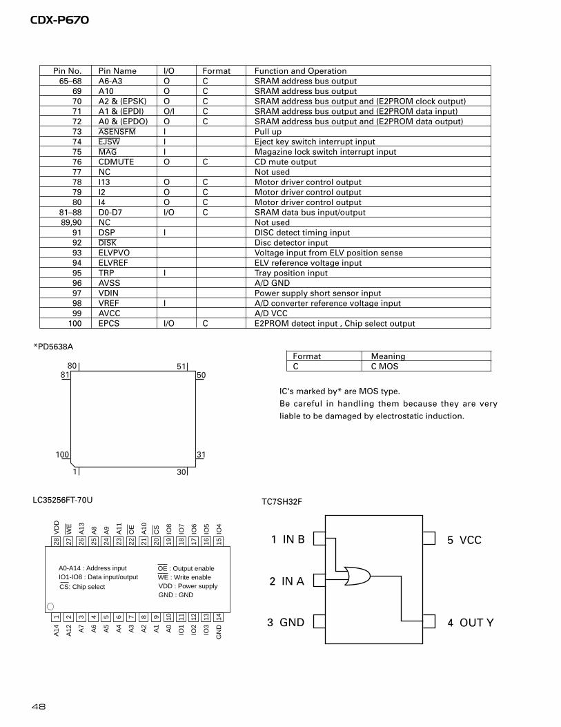
Pin No. Pin Name I/O Format Function and Operation65–68 A6-A3 O C SRAM address bus output
69 A10 O C SRAM address bus output70 A2 & (EPSK) O C SRAM address bus output and (E2PROM clock output)71 A1 & (EPDI) O/I C SRAM address bus output and (E2PROM data input)72 A0 & (EPDO) O C SRAM address bus output and (E2PROM data output)73 asensfm I Pull up74 ejsw I Eject key switch interrupt input75 mag I Magazine lock switch interrupt input76 CDMUTE O C CD mute output77 NC Not used78 I13 O C Motor driver control output79 I2 O C Motor driver control output80 I4 O C Motor driver control output
81–88 D0-D7 I/O C SRAM data bus input/output89,90 NC Not used
91 DSP I DISC detect timing input92 disk Disc detector input93 ELVPVO Voltage input from ELV position sense94 ELVREF ELV reference voltage input95 TRP I Tray position input96 AVSS A/D GND97 VDIN Power supply short sensor input98 VREF I A/D converter reference voltage input99 AVCC A/D VCC
100 EPCS I/O C E2PROM detect input , Chip select output
*PD5638AFormat MeaningC C MOS
30
31
505180
81
100
1
LC35256FT-70U
1 2 3 4 5 6 7 8 9 10 11 12 13 14
28 27 26 25 24 23 22 21 20 19 18 17 16 15
A14
A12 A7
A6
A5
A4
A3
A2
A1
A0
IO1
IO2
IO3
GN
D
VD
D
WE
A13
A8
A9
A11
OE
A10
CS
IO8
IO7
IO6
IO5
IO4
A0-A14 : Address input IO1-IO8 : Data input/output
VDD : Power supplyGND : GND
CS: Chip select
OE : Output enableWE : Write enable
TC7SH32F
1 IN B
2 IN A
3 GND 4 OUT Y
5 VCC
IC's marked by* are MOS type.
Be careful in handling them because they are very
liable to be damaged by electrostatic induction.

49
CDX-P670
VDD=5VPin16
BATT ON
bsensPin18
magPin75
bsens=L
POWER←H Pin10adena←L Pin3
VD INPin96
1.3V VD IN 2.1V
mag=L
DISC SearchPOWER←L Pin10
asensPin19
POWER←H Pin10adena←L Pin3
VD INPin96
1.3V VD IN 2.1V
POWER←LStand-by
Error message "A0"
Error message "A0"
Start the CD player
Source=Multi-CD
YES
asens=L
7.3 OPERATIONAL FLOW CHART

CDX-P670
IP-BUS cable To prevent incorrect connection, the input side ofthe IP-BUS connector is colored in blue, and theoutput side in black. Connect the connectors of thesame colors correctly.
YellowTo the terminal always supplied with powerregardless of ignition switch position.
Black (ground)To the vehicle (metal) body.
IP-BUS(black)
Fuse holder
IP-BUS output (black)Connect the black connector of the cable to thisconnector.
Connecting the Units
Multi-CD controller
600 cm
Cords for this product and those for other productsmay be different colors even if they have the samefunction. When connecting this product to anotherproduct, refer to the supplied Installation manualsof both products and connect cords that have thesame function.
GeneralSystem ..................................................... Compact disc audio systemUsable discs .................................................................... Compact DiscSignal format ....................................... Sampling frequency: 44.1 kHz
Number of quantization bits: 16; linearPower source ......................................................................... 14.4 V DC
(10.8 — 15.1 V allowable)Max. current consumption ........................................................... 1.0 AWeight ............................................................................ 1.9 kg (4.2 lbs.)Dimensions .......................................... 248 (W) × 66 (H) × 168 (D) mm
[9-3/4 (W) × 2-5/8 (H) × 6-5/8 (D) in.]Backup current ................................................................... 1mA or less
AudioFrequency characteristics ................................ 5 — 20,000 Hz (± 1 dB)Signal-to-noise ratio ............................ 92 dB (1 kHz) (IHF-A Network)Distortion ................................................................................... 0.006 %Dynamic range ................................................................. 90 dB (1 kHz)Output level ...................................................... 1,000 mV (1 kHz, 0 dB)Number of channels .............................................................. 2 (stereo)
Note:Specifications and design are subject to possible modification with-out prior notice due to improvements.
8. OPERATIONS AND SPECIFICATIONS
8.1 OPERATIONS
8.2 SPECIFICATIONS
Top Related