

![Introduction to Time-Delay Systems [10ex]lecture no. 1 · PDF fileIntroduction to Time-Delay Systems lecture no. 1 ... Linear Systems Theory. New York: Springer ... regenerative chatter](https://static.fdocuments.in/doc/165x107/5ab218e47f8b9a00728d08f4/introduction-to-time-delay-systems-10exlecture-no-1-to-time-delay-systems-lecture.jpg)


Languages
Pages
Legal


Copyright 2001, Agrawal & Bushnell
VLSI Test: Lecture 20/17alt 1
Lecture 20Delay Test
(Lecture 17alt in the Alternative Sequence)
Lecture 20Delay Test
(Lecture 17alt in the Alternative Sequence)
Delay test definition Circuit delays and event propagation Path-delay tests
Non-robust test Robust test Five-valued logic and test generation
Path-delay fault (PDF) and other fault models Test application methods
Combinational, enhanced-scan and normal-scan Variable-clock and rated-clock methods
At-speed test Timing design and delay test Summary

Copyright 2001, Agrawal & Bushnell
VLSI Test: Lecture 20/17alt 2
Delay Test DefinitionDelay Test Definition
A circuit that passes delay test must produce correct outputs when inputs are applied and outputs observed with specified timing.
For a combinational or synchronous sequential circuit, delay test verifies the limits of delay in combinational logic.
Delay test problem for asynchronous circuits is complex and not well understood.
Copyright 2001, Agrawal & Bushnell
VLSI Test: Lecture 20/17alt 3
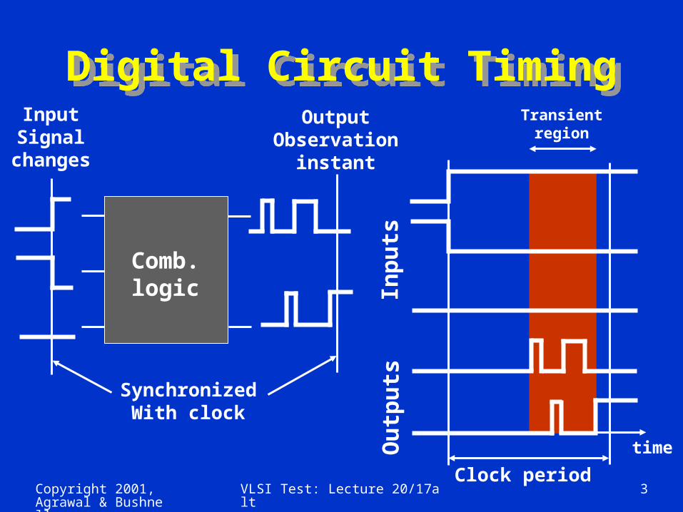
Digital Circuit TimingDigital Circuit Timing
Inp
uts
Ou
tpu
ts
time
Transientregion
Clock period
Comb.logic
OutputObservation
instant
InputSignal
changes
SynchronizedWith clock

Copyright 2001, Agrawal & Bushnell
VLSI Test: Lecture 20/17alt 4
Circuit DelaysCircuit Delays Switching or inertial delay is the interval between input change
and output change of a gate: Depends on input capacitance, device (transistor)
characteristics and output capacitance of gate. Also depends on input rise or fall times and states of other
inputs (second-order effects). Approximation: fixed rise and fall delays (or min-max delay
range, or single fixed delay) for gate output. Propagation or interconnect delay is the time a transition
takes to travel between gates: Depends on transmission line effects (distributed R, L, C
parameters, length and loading) of routing paths. Approximation: modeled as lumped delays for gate inputs.
See Section 5.3.5 for timing models.

Copyright 2001, Agrawal & Bushnell
VLSI Test: Lecture 20/17alt 5
Event Propagation Delays
Event Propagation Delays
2 4 61
1 3
5
3
10
0
0
2
2
Path P1
P2
P3
Single lumped inertial delay modeled for each gatePI transitions assumed to occur without time skew
Copyright 2001, Agrawal & Bushnell
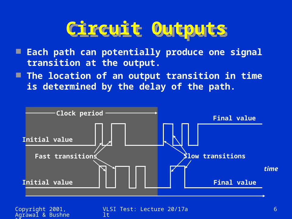
VLSI Test: Lecture 20/17alt 6
Circuit OutputsCircuit Outputs Each path can potentially produce one signal
transition at the output. The location of an output transition in time is
determined by the delay of the path.
Initial value
Initial value
Final value
Final value
Clock period
Fast transitions Slow transitions
time
Copyright 2001, Agrawal & Bushnell
VLSI Test: Lecture 20/17alt 7
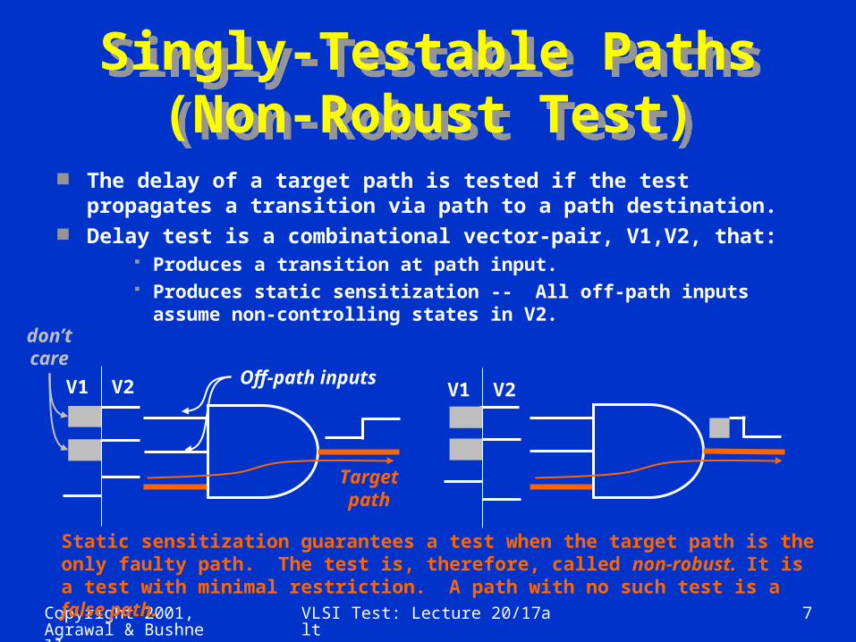
Singly-Testable Paths(Non-Robust Test)
Singly-Testable Paths(Non-Robust Test)
The delay of a target path is tested if the test propagates a transition via path to a path destination.
Delay test is a combinational vector-pair, V1,V2, that: Produces a transition at path input. Produces static sensitization -- All off-path inputs assume
non-controlling states in V2.
V1 V2 V1 V2
Static sensitization guarantees a test when the target path is the only faulty path. The test is, therefore, called non-robust. It is a test with minimal restriction. A path with no such test is a false path.
Targetpath
Off-path inputs
don’tcare

Copyright 2001, Agrawal & Bushnell
VLSI Test: Lecture 20/17alt 8
Robust TestRobust Test A robust test guarantees the detection of a delay
fault of the target path, irrespective of delay faults on other paths.
A robust test is a combinational vector-pair, V1, V2, that satisfies following conditions:
Produce real events (different steady-state values for V1 and V2) on all on-path signals.
All on-path signals must have controlling events arriving via the target path.
A robust test is also a non-robust test. Concept of robust test is general – robust tests for
other fault models can be defined.

Copyright 2001, Agrawal & Bushnell
VLSI Test: Lecture 20/17alt 9
Robust Test ConditionsRobust Test Conditions
Real events on target path. Controlling events via target path.
V1 V2 V1 V2
V1 V2
V1 V2
V1 V2
V1 V2
U1
U1
U1/R1
S1
U0/F0
S1
U0
U0
U0/F0
U1/R1
U1/R1
U1/R1U0/F0
U0/F0
S0
S0
Copyright 2001, Agrawal & Bushnell
VLSI Test: Lecture 20/17alt 10
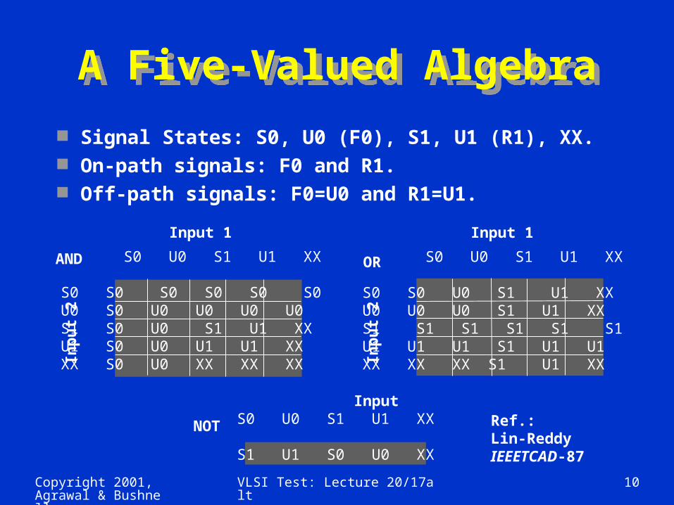
A Five-Valued AlgebraA Five-Valued Algebra
Signal States: S0, U0 (F0), S1, U1 (R1), XX. On-path signals: F0 and R1. Off-path signals: F0=U0 and R1=U1.
S0 U0 S1 U1 XX
S0 S0 S0 S0 S0 S0U0 S0 U0 U0 U0 U0S1 S0 U0 S1 U1 XXU1 S0 U0 U1 U1 XXXX S0 U0 XX XX XX
Input 1
Inp
ut
2
S0 U0 S1 U1 XX
S0 S0 U0 S1 U1 XXU0 U0 U0 S1 U1 XXS1 S1 S1 S1 S1 S1U1 U1 U1 S1 U1 U1XX XX XX S1 U1 XX
Input 1
Inp
ut
2
InputS0 U0 S1 U1 XX
S1 U1 S0 U0 XX
AND OR
NOT Ref.:Lin-ReddyIEEETCAD-87

Copyright 2001, Agrawal & Bushnell
VLSI Test: Lecture 20/17alt 11
Robust Test GenerationRobust Test Generation
R1
S0U0
R1
XX S0
U0
F0
U0
Path P3
Test for ↓ P3 – falling transition through path P3: Steps A through E
F0
XX
A. Place F0 at path origin
B. Propagate F0 through OR gate; also propagates as R1 through NOT gate
C. F0 interpreted as U0; propagates through AND gate
D. Change off-path input to S0 to Propagate R1 through OR gate
E. Set input of AND gate to S0 to justify S0 at output
Robust Test:S0, F0, U0

Copyright 2001, Agrawal & Bushnell
VLSI Test: Lecture 20/17alt 12
Non-Robust Test GenerationNon-Robust Test Generation
U1
U0
XX U1
U0
R1
R1
Path P2
Fault ↑ P2 – rising transition through path P2 has no robust test.
R1
XX
A. Place R1 at path origin
B. Propagate R1 through OR gate; interpreted as U1 on off-path signal; propagates as U0 through NOT gate
D. R1 non-robustly propagates through OR gate since off- path input is not S0
C. Set input of AND gate to propagate R1 to output
Non-robust test:U1, R1, U0
U1 Non-robust test requiresStatic sensitization:S0=U0, S1=U1
R1

Copyright 2001, Agrawal & Bushnell
VLSI Test: Lecture 20/17alt 13
Path-Delay Faults (PDF)Path-Delay Faults (PDF) Two PDFs (rising and falling transitions) for each physical path. Total number of paths is an exponential function of gates. Critical
paths, identified by static timing analysis (e.g., Primetime from Synopsys), must be tested.
PDF tests are delay-independent. Robust tests are preferred, but some paths have only non-robust tests.
Three types of PDFs (Gharaybeh, et al., JETTA, 1997): Singly-testable PDF – has a non-robust or robust test. Multiply-testable PDF – a set of singly untestable faults that has a
non-robust or robust test. Also known as functionally testable PDF.
Untestable PDF – a PDF that is neither singly nor multiply testable. A singly-testable PDF has at least one single-input change (SIC)
non-robust test.

Copyright 2001, Agrawal & Bushnell
VLSI Test: Lecture 20/17alt 14
Other Delay Fault Models
Other Delay Fault Models
Segment-delay fault – A segment of an I/O path is assumed to have large delay such that all paths containing the segment become faulty.
Transition fault – A segment-delay fault with segment of unit length (single gate):
Two faults per gate; slow-to-rise and slow-to-fall. Tests are similar to stuck-at fault tests. For example, a line is
initialized to 0 and then tested for s-a-0 fault to detect slow-to-rise transition fault.
Models spot (or gross) delay defects. Line-delay fault – A transition fault tested through the longest
delay path. Two faults per line or gate. Tests are dependent on modeled delays of gates.
Gate-delay fault – A gate is assumed to have a delay increase of certain amount (called fault size) while all other gates retain some nominal delays. Gate-delay faults only of certain sizes may be detectable.
Copyright 2001, Agrawal & Bushnell
VLSI Test: Lecture 20/17alt 15
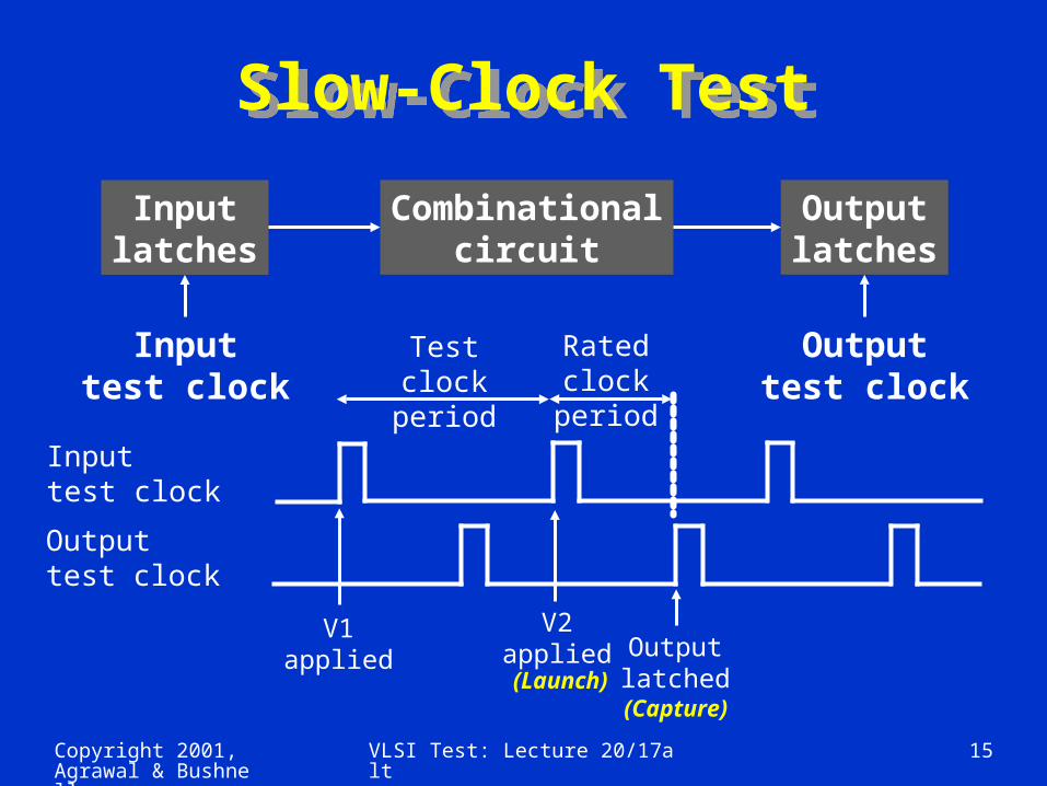
Slow-Clock TestSlow-Clock Test
Inputtest clock
Outputtest clock
Combinationalcircuit
Inputlatches
Outputlatches
Inputtest clock
Outputtest clock
V1applied
V2applied Output
latched
Testclockperiod
Ratedclockperiod
(Launch) (Capture)

Copyright 2001, Agrawal & Bushnell
VLSI Test: Lecture 20/17alt 16
Enhanced-Scan TestEnhanced-Scan Test
Combinational
circuit
HL
SFFHL
SFF
PI PO
SCANIN
SCAN-OUT
HOLDCK TC
CK TC
CK: system clockTC: test controlHOLD: hold signalSFF: scan flip-flopHL: hold latch
CK
HOLD
CKperiod
No
rma
lm
od
e
No
rma
lm
od
e
TCScan mode
V1 PIapplied
V2 PI appliedLaunch
ScaninV1
states
ScaninV2 states
V1 settles
Result latchedCapture
Scanoutresult

Copyright 2001, Agrawal & Bushnell
VLSI Test: Lecture 20/17alt 17
Normal-Scan TestNormal-Scan Test
Combinational
circuit
SFF
SFF
PI PO
SCANIN
SCAN-OUT
CK TC
CK TC
CK: system clockTC: test controlSFF: scan flip-flop
RatedCK period
No
rma
lm
od
e
TC(A)
LOSScan mode
V1 PIsapplied
LaunchV2 PIsapplied
ScaninV1 states
CaptureResultlatched
Resultscanout
V2 states generated, (A) Launch-off-shift (LOS), by one-bit scan shift of V1, or
(B) Launch-off-capture (LOC), by V1 applied in functional mode.
Scan mode
Normal mode
TC(B)
LOCScan modeScan mode
Slow CKperiod
t
Gen. V2states
Pathtested
Slow clock

Copyright 2001, Agrawal & Bushnell
VLSI Test: Lecture 20/17alt 18
Variable-Clock Sequential Test
Variable-Clock Sequential Test
T 1
PI
PO
T n-2
PI
PO
T n-1
PI
PO
T n+1
PI
PO
T n+m
PI
PO
1
2
1 1
22
T n
PI
PO
Initialization sequence(slow clock)
Pathactivation
(ratedClock)
Fault effectpropagation
sequence(slow clock)
0
0
1
D
Off-pathflip-flop
Note: Slow-clock makes the circuit fault-free in the presence of delay faults.

Copyright 2001, Agrawal & Bushnell
VLSI Test: Lecture 20/17alt 19
Variable-Clock ModelsVariable-Clock Models Fault effect propagation can be affected by ambiguous states of
off-path flip-flops at the end of the rated-clock time-frame (Chakraborty, et al., IEEETCAD, Nov. 1997):
Fault model A – Off-path flip-flops assumed to be in correct states; sequential non-robust test (optimistic).
Fault model B – Off-path flip-flops assumed to be in unknown state; sequential robust test (pessimistic).
Fault model C – Off-path flip-flops in steady (hazard-free) state retain their correct values, while others assume unknown state; sequential robust test.
Test length: A test sequence of N vectors is repeated N times, with a different vector applied at rated-clock each time.
Test time ~ N2 x (slow-clock period)
Copyright 2001, Agrawal & Bushnell
VLSI Test: Lecture 20/17alt 20
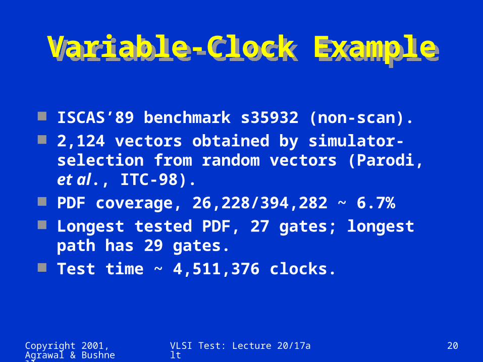
Variable-Clock ExampleVariable-Clock Example
ISCAS’89 benchmark s35932 (non-scan). 2,124 vectors obtained by simulator-selection
from random vectors (Parodi, et al., ITC-98). PDF coverage, 26,228/394,282 ~ 6.7% Longest tested PDF, 27 gates; longest path has
29 gates. Test time ~ 4,511,376 clocks.
Copyright 2001, Agrawal & Bushnell
VLSI Test: Lecture 20/17alt 21
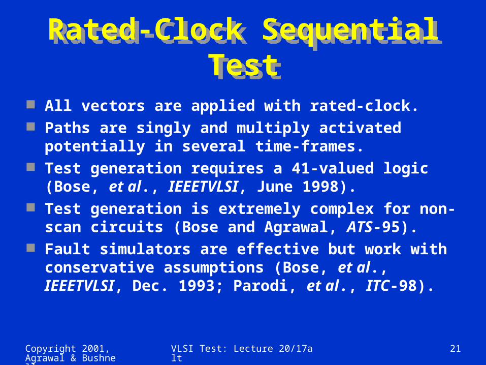
Rated-Clock Sequential TestRated-Clock Sequential Test
All vectors are applied with rated-clock. Paths are singly and multiply activated potentially in
several time-frames. Test generation requires a 41-valued logic (Bose, et
al., IEEETVLSI, June 1998). Test generation is extremely complex for non-scan
circuits (Bose and Agrawal, ATS-95). Fault simulators are effective but work with
conservative assumptions (Bose, et al., IEEETVLSI, Dec. 1993; Parodi, et al., ITC-98).
Copyright 2001, Agrawal & Bushnell
VLSI Test: Lecture 20/17alt 22
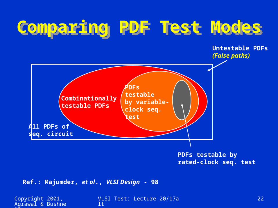
Comparing PDF Test ModesComparing PDF Test Modes
All PDFs ofseq. circuit
Combinationallytestable PDFs
PDFstestableby variable-clock seq.test
PDFs testable byrated-clock seq. test
Ref.: Majumder, et al., VLSI Design - 98
Untestable PDFs(False paths)

Copyright 2001, Agrawal & Bushnell
VLSI Test: Lecture 20/17alt 23
At-Speed TestAt-Speed Test At-speed test means application of test vectors at the rated-
clock speed. Two methods of at-speed test. External test:
Vectors may test one or more functional critical (longest delay) paths and a large percentage (~100%) of transition faults.
High-speed testers are expensive. Built-in self-test (BIST):
Hardware-generated random vectors applied to combinational or sequential logic.
Only clock is externally supplied. Non-functional paths that are longer than the functional
critical path can be activated and cause a good circuit to fail.
Some circuits have initialization problem.
Copyright 2001, Agrawal & Bushnell
VLSI Test: Lecture 20/17alt 24
Timing Design & Delay TestTiming Design & Delay Test
Timing simulation: Critical paths are identified by static (vector-less) timing
analysis tools like Primetime (Synopsys). Timing or circuit-level simulation using designer-
generated functional vectors verifies the design. Layout optimization: Critical path data are used in
placement and routing. Delay parameter extraction, timing simulation and layout are repeated for iterative improvement.
Testing: Some form of at-speed test is necessary. PDFs for critical paths and all transition faults are tested.

Copyright 2001, Agrawal & Bushnell
VLSI Test: Lecture 20/17alt 25
SummarySummary Path-delay fault (PDF) models distributed delay defects. It
verifies the timing performance of a manufactured circuit. Transition fault models spot delay defects and is testable by
modified stuck-at fault tests. Variable-clock method can test delay faults but the test time
can be long. Scan testing allows two options: Launch off shift (LOS) Launch off capture (LOC)
Critical paths of non-scan sequential circuits can be effectively tested only by rated-clock tests.
Delay test methods (including BIST) for non-scan sequential circuits using slow ATE require investigation:
Suppression of non-functional path activation in BIST. Difficulty of rated-clock PDF test generation. Long sequences of variable-clock tests.
Top Related