


Languages
Pages
Legal


TI Information – Selective Disclosure
Boost Converter & Controller Solutions New Products/Reference design Update
BCS / BMC, TI
1Q 2019
1

TI Information – Selective Disclosure
Agenda
•BCS overview
•New Products & Reference Design
2 2

TI Information – Selective Disclosure
BCS Different Device
Vin
Vout
Boost Converter
Vin
Vout
Boost Controller
Vin Vout
Boost-Buck Converter/Controller

TI Information – Selective Disclosure
BCS Products Overview
4
Type Prefix
Boost
Converters
TPS61xxx
TLV61xxx
TPS81xxx
TPS55xxx
LM500x
LMR6xxxx
Type Prefix
Boost
Controllers
TPS43xxx
LM34xx
LM50xx
LM51xx
Type Prefix
Buck / Boost
Controllers
(>20V)
TPS43xxx
LM25xxx
LM51xx
Type Prefix
Charge Pumps
& PWM
Modulator
MC330xx
LT10xx
TPS60xxx
Type Prefix
Buck / Boost
Converters
(>20V)
TPIC741xx
TPS55xxx
LMR705xx

TI Information – Selective Disclosure
Boost also could be used as Flyback and Sepic
5
GATE
CS
SS COMP FB
VCC
GND
VLOAD
RT
BIAS
UVLO/SYNC
LM5155
Non-Isolated Flyback
VSUPPLY
UVLO/SYNC CS
LM5155 GND
RT
SS
GATE
COMP FB
VCC
VLOAD
BIAS
PSR Flyback VSUPPLY
UVLO/SYNC CS
LM5155 GND
SS VCC COMP FB
GATE
RT
BIAS
Sepic
VSUPPLY
VLOAD
VLOAD
UVLO
GATE
CS
SS VCC COMP FB
LM5155 GND
RT
BIAS
VSUPPLY
VLOAD
+VLOAD (100V)
-V LOAD (-100V)
Dual output sepic
GATE
CS
SS VCC COMP FB
LM5155 GND
-V SUPPLY
+VLOAD
BIAS
UVLO
RT
Negative-to-Positive Converter
UVLO/SYNC CS
LM5155 GND
RT
SS FB
GATE
COMP
VCC
VLOAD
BIAS
VSUPPLY
Isolated Flyback
Optional
VLOAD
EVM@RTM
EVM@RTM

TI Information – Selective Disclosure
BCS Flyback Advantage Vs. Offline Flyback
BCS Flyback Offline Flyback
Target Application DC-DC or need Wide Vin Range AC-DC
AC-DC
Minimum Input Voltage 3.5V 10V
Shutdown IQ 2.6uA No shutdown pin
Non-switching IQ in Active 480uA 2.3mA + VDD Zener clamp leak

TI Information – Selective Disclosure
BCS Flyback Exmple
30~800Vin 21Vo/1.5A

TI Information – Selective Disclosure
How to Calculate Boost Output Current?
Iout = (ILIM * Vin / Vout) * ŋ
ILIM = 1.7A MIN
Condition: Vin = 1V, Vout = 3V, Iout = 0.5A, ŋ = 90%

TI Information – Selective Disclosure
How to Calculate the Boost Iq Roughly?
Total IQ = IQin + (IQout *Vout/Vin)/ŋ
Total IQ = 0.4 + (0.6 * 3/1.5)/89% = 1.8uA
Condition: Vin = 1.5V, Vout = 3V, Iout = 10mA ŋ = 89%

TI Information – Selective Disclosure
For Details, Please see below link.
Do you know How to calculate BOOST Iout?
Do you know How to calculate BOOST Iq?

TI Information – Selective Disclosure
Boost Converter(Internal Power FET)
TI Information – Selective Disclosure
Sync
2.5V~12Vin
Up to 12.6Vout
7A Isw min
High-VOUT Boost Converter
TPS61170 2x2 QFN-6
Async 3~18Vin Up to 38Vout 0.96A Isw min
TPS61175 HTSSOP-14
Async
2.9~18Vin
Up to 38Vout
3A Isw min
TPS61040/1 TSOT23-5; 2x2
QFN6
1.8~6Vin
Up to 28Vout
0.25/0.4A Isw
28uA Iq
TPS61045 3x3 QFN-8
1.8~6Vin
Up to 28Vout
40uA Iq
True shutdown
TPS61080/1 3x3 QFN-10
Power diode integrated
2.5~6Vin
Up to 27Vout
0.7A/1.6A Isw
True shutdown
TPS61085 MSOP/TSSOP-8
Async
2.3~6Vin
Up to 18.5Vout
2.0A Isw min
100uA max. Iq
TPS61087 3x3 QFN-10
Async
2.5V~6Vin
Up to 18.5Vout
3A Isw min
100uA max. Iq
TPS61093 2.5x2.5 QFN-10
Power diode integrated
1.6~6Vin
Up to 17Vout
0.9A Isw
True shutdown
ISW peak
2A 1A <0.5A
30V
20V
40V
VOUT MAX
3A
12V
10A
EXISTING
TLV/TPS61046 SOT23-6 WCSP-6
Diode integrated
1.8V~6Vin
Up to 28Vout
0.7A Isw
1.0uA max. Isd
True shutdown
Sync
2.5V~10Vin
Up to 12.6Vout
10A Isw min
TPS61088 3.5x4.5 QFN-20
Sync
2.7V~20Vin
Up to 20Vout
Load disconnect
10A Isw min
TPS61178 3.5x3 QFN-13
TPS61089 2x2.5 QFN
NEW
DEVELOPMENT
TPS55330 WQFN-16
LMR61428 VSSOP-8
LMR62421 WSON-6 SOT23-5
TPS55340 WQFN-16, HTSSOP-14
LM5000 TSSOP-16 WSON-16
TPS55332 HTSSOP-20
LM5001 SOIC-8,WSON-8
LM5002 SOIC-8,WSON-8 8
0V
LM2731 SOT23-5
LM3224 VSSOP-8
LM4510 WSON-10
LM27313 SOT23-5
LMR64010 SOT23-5
LM2733 SOT23-5
LM2622 VSSOP-8
LM2698 VSSOP-8
LM2700 TSSOP-14 WSON-14
LM2705 SOT23-5
LMR62014 SOT23-5
Async 2.2~7Vin Up to 20Vout 150mA Isw min
Sync 2.7~5.5Vin Up to 18Vout 1A Isw min True Shutdown
Async 2.7~14Vin Up to 20Vout 1.4A Isw min
2.7~7Vin
Up to 20Vout
1.9A Isw min
615kHz/1.25MHz Pin
Selectable Frequency
Async 2.7~14Vin Up to 20Vout 1.4A Isw min
Async 2.9~16Vin Up to 22Vout 5.25A Isw min
Async 2.2~12Vin Up to 17.5Vout 2.55A Isw min
Async 1.2~14Vin Up to 14Vout 2.2A Isw min
Async 2.7~14Vin Up to 38Vout 1A Isw
1.5~40Vin
Up to 50Vout
5.25A Isw min
Async 2.9~32Vin Up to 38Vout 5.25A Isw min
Async 3.1~75Vin Up to 75Vout 0.8A Isw
Async 3.1~40Vin Up to 80Vout 1.35A Isw min
Async 2.7~14Vin Up to 40Vout 1A Isw min
Async 2.7~14Vin Up to 28Vout 0.8A Isw min
Async 3.1~75Vin Up to 75Vout 0.4A Isw min
Async 2.7~5.5Vin Up to 24Vout 2.1A Isw min
Async 2.0~12Vin Up to 18Vout 1A Isw min
Async 2.2~12Vin Up to 18Vout 1.35A Isw min
5A
TPS61372 1.5x1.5 BGA-16
Sync
1.8V~5.5Vin
Up to 20Vout
3.8A Isw typ
Low-Iq
TPS61390 3x3 QFN-20
2.7~5.5Vin
Up to 85Vout
Integrated Rectifier Diode
Sample / Hold Integrated

TI Information – Selective Disclosure
TPS6102x 3x3 QFN-10
Sync
0.9~6.5Vin
Up to 5.5Vout
1.8A Isw
Down mode
True shutdown
Sync
0.9~5Vin
200mA Isw
5nA for bypass
ISW peak
2A 1A 0.5A
0.3
V
VIN MIN
3A
TPS6122x SC70-6
Sync
0.7~5.5Vin
Up to 6Vout
0.4A Isw
5.5uA Iq
Low-VIN Boost Converter 0
.9V
1
.8V
TPS61045 3x3 QFN-8
Async
1.8~6Vin
Up to 28Vout
0.375A Isw
40uA Iq
True shutdown
TPS6120x 3x3 QFN-10
Sync
0.3~5.5Vin, Up to 5.5Vout
1.35A Isw
55uA Iq
True shutdown
TPS61030/1/2
4x4 QFN/TSSOP-16
Sync
1.8~5.5Vin
Up to 5.5Vout
3A Isw
20uA Iq
True shutdown
TPS61090/1/2
4x4 QFN-16
Sync
1.8~5.5Vin
Up to 5.5Vout
2.2A Isw
20uA Iq
True shutdown
TPS61093
2.5x2.5 QFN-10
Power diode integr.
1.6~6Vin
Up tp 17Vout
1.1A Isw
True shutdown
TPS61071 TSOT23-6
Sync
0.9~6.5Vin
Up to 5.5Vout
0.6A Isw
20uA Iq
PFM/PWM
True shutdown
TPS61260/1
2x2 QFN-6
Sync
0.8~4Vin
Up to 4Vout
0.7A Isw
Adjustable Iout
29uA Iq
True shutdown
TPS61040
SOT23; 2x2 QFN
Async
1.8~6Vin
Up to 28Vout
0.25/0.4A Isw
28uA Iq
TPS61098 1.5x1.5 QFN-6
Sync
0.7~5.0Vin
Dual outputs
Integr. load sw/LDO
0.6A Isw
300nA Iq
Pass-through
TPS61046 0.8x1.2 WCSP-6
Diode integrated
1.8V~6Vin
Up to 28Vout
0.7A Isw
1.0uA max. Isd
True shutdown
TPS61029
2x2 SON-10
Sync
1.5V~5Vin
2.5, 3.0, 3.3Vout
0.7A Isw
0.5uA max. Isd
bypass shutdown
TPS61021A 2x2 WSON-8
Sync
0.5~4.4Vin
1.8~4.0Vout
3.0A Isw
<30uA Iq
Load disconnect
TPS61099
1.3x0.9 WCSP
TPS61096A 2x3 QFN
1.8~5.5Vin
28Vout
ISW 0.5A
1uA iq
0.7~5.5V in
5.5Vout
0.8A ISW
0.8uA Iq
EXISTING
NEW
DEVELOPMENT
LM2623 WSON,
VSSOP-8
0.8~14Vin
Up to 14Vout
2.2A Isw
LM2621 VSSOP-8
1.2~5Vin
Up to 14Vout
2.2A Isw
TPS61291 2x2 SON
Sync
0.9~5Vin
700mA Isw
15nA for bypass
TPS61097A SOT23-5
TPS61022 2x2 QFN-7
Sync
1.8V startup voltage
0.5~5.5Vin
Up to 5.5V Vout
9A Isw
<30uA Iq
Load disconnect
Low-Iq
TPS61322x SOT23-3
Sync
0.9~5.5Vin
6.5uA Iq
0.75/1.2/1.8A
Low Cost
9A
TPS61095
2x2 QFN-8
100nA Iq
0.7~5.5V Vin
6.0Vout
1.8A ISW
Isw adjustable

TI Information – Selective Disclosure
Li+ Battery Input Boost Converter
TPS61093 2.5x2.5 QFN-10
Power diode integrated
1.6~6Vin
Up to 17Vout
1.1A Isw
True shutdown
ISW peak
2A 1A
>12
Vo
ut
6V
ou
t
VOUT MAX
8A
Sync
2.5V~10Vin
Up to 12.6Vout
10A Isw
50uA max. IQ
TPS61088 3.5x4.5 QFN-20
5A
TPS61046 0.8x1.2 WCSP-6
Diode integrated
1.8V~6Vin
Up to 28Vout
0.7A Isw
1.0uA max. Isd
True shutdown
TPS61240/1 1.3x0.9 WCSP-6
Sync: 250/290mΩ
2.3~5.5Vin
5Vout
0.6/0.7A Isw_valley
30uA Iq
True shutdown
TPS61251/2 2x2 QFN-8
Sync: 130/200mΩ
2.3~6Vin
Up to 6.5Vout
Adjustable IIN up to
1.5A
30uA Iq
2uA snooze
mode(151)
True shutdown
TPS6125x 1.3x0.9 WCSP-6
Sync: 100/170mΩ
2.3~5.5Vin
Up to 5.1Vout
2.15/3.62A
Isw_valley
37uA Iq
Bypass mode
TPS61280/1/2 1.7x1.7 WCSP-16
Sync: 45/40mΩ
2.3~4.8Vin
Up to 4.7Vout
3/4A Isw_valley
55uA Iq
In-out auto bypass
TPS61235/6 2.5x2.5 QFN-14
Sync: 14/14mΩ
2.3~5.5Vin
Up to 5.5Vout
8A Isw_valley
20uA Iq
Adjustable Iout limit
True shutdown
Sync
2.7V~12Vin
Up to 12.6Vout
7A Isw
250uA max Iq
TPS61089 2x2.5 QFN
Sync
2.7V~20Vin
Up to 20Vout
10A Isw
Load disconnect
TPS61178 3.5x3 QFN-13
Sync: 22 / 20 mΩ
2.5V~5.5Vin
Up to 5.5Vout
6A Isw
TPS61230A 2x2 QFN-7
TPS6125xA 1.3x0.9 WCSP-6
Sync: 50 / 60mΩ
2.3V~5.5Vin
Up to 5.5Vout
4A Isw
PFM/PWM/Ultrasonic
Bypass
EXISTING
NEW
DEVELOPMENT

TI Information – Selective Disclosure
Buck-Boost Controller/Converter & Boost Controller(>=40V)

TI Information – Selective Disclosure
VIN Buck-Boost Controller/Converter & Boost Controller
8A
Maxim
um
In
du
cto
r C
urr
en
t
25A
15A
15A
LM5020
LM5121/22
40V
75V
48V 100V 65V
50V
Boost Controller
25A
LM5118 LM25118
42V
LM5175
VIN
VOUT
LM5022
52V
TPS40210
LM3481
100V
Buck-Boost Controller/Converter
60V
LM5176
LM5150
40A LM5170
2A
Non-Sync
Synchronous
Development
Converter
LM25122-Q1
TPS43060/61
LM3478/88
TPS55160/5
TPIC74101/0
TPS55065
LM5155
TPS55288

TI Information – Selective Disclosure
Charge Pump(Boost/Buck-Boost/Inverter)

TI Information – Selective Disclosure
TL7660
Charge Pump(Boost/Inverter/Buck-Boost)
Vin 0.8V 0.9V 1.8V 2.5V 2.7V 3.3V 6.0V 5.4V 6.5V 10V 12V 3.6V
300mA
250mA
200mA
150mA
100mA
60mA
50mA
30mA
20mA
Iout
TPS6030xx
TPS6024x
RRG711-x
TPS6020x, 6021x
TPS60400
REG710-x
TPS6014x
TPS6010x,6012x,6020x,6021x
TPS60150
TPS60101
TPS6010x, 6012x
TPS60110,6013x 5V
3.3V
5V
2.5V,2.7V,3.0V,3.3V,5V
-1.6V to -5.5V
3.3V
2.5V,2.7V,3.0V,3.3V,5V
3.0V, 3.3V
2.7V,3.0V,3.3V,5V
3.0V,3.3V
5V
5V
Inverter
Boost
Buck-Boost
LM2776
LM27762 ±1.5V to ± 5V
-2.7V to -5.5V
LM2775 5V
LM2750 5V, 3.8V to 5.2V
LM2765,2766,2767 3.6V to 11V
LM27761 -1.5V to - 5V
LM2682 -4V to -11V
-1.5V to -10V
Low-Iq

TI Information – Selective Disclosure
FEATURES BENEFITS
APPLICATIONS
TPS61022 High current 5V, 9A boost converter with input voltage down to 0.5V
• Input voltage range: 0.5V to 5.5V
• Startup voltage: 1.8V
• Output voltage range: Vin to 5.5V
• Typical 20µA quiescent current from Vout
• Pass-through when Vin > Vout
• Valley current limit: 6.5A min, 9A typical
• Rdson: 13mΩ low side and 18mΩ high side
• Pin-selectable PFM / Forced PWM in light load
• Internal 1ms soft start time
• True disconnection during shutdown
• 1.0MHz/500kHz switching frequency operation
• Available in 2mm x 2mm hotrod QFN package
• Low input voltage
• Large output current
• Smallest solution in industry
• Super Cap
• USB Port
• LED torch
VIN
EN
SW
VOUT
FB
GND
L1
R1
R2
OFF
ON
C1
C2
0.5V ~ 5.0V
1.0µH
TPS61022
5.0V
MODEPFM
PWM
MODE
EN
VIN
VOUT
SW
GND
FB
Sample Now
RTM in 1Q19

TI Information – Selective Disclosure
Backup power: Boosted GPRS/LTE power(PMP30528)
3.6V/500mA
2A peak
1-Cell
Super-CAP
Discrete
charger
0.7V~2.7V
12V 3.8V/500mA
2A peak 220VAC AC-DC
Buck
TPS62160
Boost
TPS61022
New!
GPRS/LTE
module
Target end
equipments:
• E-meter
• Data concentrator
• HVAC valve and
pump control
Switch
Circuit
Boost(300nA)
TPS610981
MCU
(Optional)
3.3V/50mA

TI Information – Selective Disclosure
Features Benefits
LM5155x 2.2MHz Wide VIN Non-synchronous Boost/Flyback/Sepic
Applications
• AEC-Q100 grade 1 qualified (TA = -40ºC to 125ºC, TJ = -40ºC to 150ºC)
• Wide input range : 3.5V~ 45V
(2.97V ~ 16V when BIAS=VCC, 1.5V~45V when BIAS≥2.97V)
• Programmable frequency 100kHz to 2.2MHz with clock synchronization
• Shutdown IQ ≤5uA
• Non-switching IQ ≤ 450uA
• 1.5A peak gate driver
• 100mV current limit threshold with optional hiccup mode protection
• 1.0V +/-1% reference
• Adjustable slope compensation
• Programmable line UVLO
• Adjustable soft-start
• PGOOD indicator
• OVP protection
• Thermal shutdown
• 12pin-WSON package (3mmx2mm) with Wettable Flanks
• General purpose Boost / Sepic
• Battery powered application
• Automotive LED headlights
• Industrial Flyback power supply/ Primary side controlled Flyback
• Boost/Sepic/Flyback(Non-isolated/isolated) configurable
• Wide VIN for a variety of power rails including 1-cell battery
• Switching frequency out of AM band
• Small solution size at 2.2MHz
• Low shutdown IQ reduces battery drain in battery-powered application
• Low current limit threshold minimizes power loss
• Optional hiccup mode for sustained overload / short-circuit protection
• Allows high step-up ratio using SYNC
BIAS VCC
GATE UVLO/SYNC CS
LM5155
SS
PGND
FB
COMP
AGND
PGOOD
RT
VSUPPL
Y VLOAD
Hiccup mode protection
Disabled Enabled
LM5155 LM51551
2
1

TI Information – Selective Disclosure
Performance Comparison
Parameter LM5155x LM3481 TPS40210 LM5022 LM5150x
Vin Range 3.5 - 45V
Min 1.5V when BIAS>3.5V 2.97 – 48V 4.5 – 52V 6 – 60V
5-42V
1.5V when VOUT>5V
Max FSW 2.2MHz 1MHz 1MHz 2.2MHz 2.3MHz
Driver Strength 1.5A 1A 0.4A 1A 1.5A
Ext Power MOSFET
supported Logic,Standard.
Logic,Std.
2.5V MOSFET Logic,Std. Logic,Std. Logic
Current Limit Threshold 100mV+/-10% 160mV+19%/-38% 150mV 500mV 120m
Hiccup Mode Protection Yes
(LM5155 enabled, -1 disabled) No
Yes
but cannot disable No No
EN and UVLO EN and UVLO UVLO/Shutdown Inverted Enable UVLO EN
FB reference voltage 1V+/-1.0% 1.275V+/-1.5% 0.7V+/-2% 1.25V +/-2% +/-2% including FB
Res.
Shutdown IQ 1u~5uA 5uA 10uA 350uA 5~6uA
Non-switching IQ <[email protected] 3700uA 1500uA 3500uA 15~16uA
Min Ton [email protected]
100ns@100kHz Max 570ns 75ns 65ns 50n
OVP, PGOOD OVP, PGOOD OVP None None None
Package (X x Y mm)
WSON-12
Leadless WettableFlanks
3 mm x 2 mm
VSSOP-10 Leaded
3 mm x 3 mm
VSSOP-10 Leaded
3 mm x 5 mm
VSSOP-10 Leaded
3 mm x 3 mm
WQFN-16 WF
4mm x 4mm
22
TI Information – Selective Disclosure
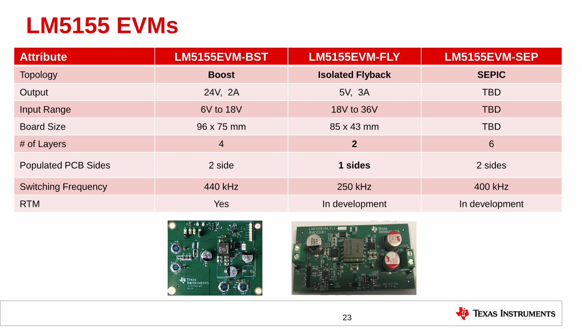
LM5155 EVMs
Attribute LM5155EVM-BST LM5155EVM-FLY LM5155EVM-SEP
Topology Boost Isolated Flyback SEPIC
Output 24V, 2A 5V, 3A TBD
Input Range 6V to 18V 18V to 36V TBD
Board Size 96 x 75 mm 85 x 43 mm TBD
# of Layers 4 2 6
Populated PCB Sides 2 side 1 sides 2 sides
Switching Frequency 440 kHz 250 kHz 400 kHz
RTM Yes In development In development
23

TI Information – Selective Disclosure
LM5155EVM-FLY Flyback Evaluation Board
• 2OZ, 2-layer design
• All components are mounted on top
• High Efficiency >84% (peak)
• Easy access to IC pins, including PGOOD, COMP, SS
• Protection features including cycle-by-cycle current
limit, Hiccup mode overload protection, TSD
• Reserved foot prints for primary-side regulation
configuration
• Reserved foot prints for primary-side soft-start
43
mm
85mm
LM5155EVM-FLY
Input voltage range 18V~36V
Output regulation target 5
Load current Max 3A
Switching Freq. 250kHz
Features

TI Information – Selective Disclosure
LM5155EVM-BST Boost Evaluation Board
• High Efficiency >97% (peak)
• Easy access to IC pins, including UVLO/SYNC, SS,
COMP, PGOOD, BIAS, VCC
• Protection features including cycle-by-cycle current
limit, OVP, TSD
• Multiple BIAS pin and VCC pin connections to test
multiple configurations – BIAS connect to VCC
– BIAS supplied with external power supply
– VCC supplied by external power supply
– BIAS supplied by output voltage
• Reserved differential mode filter foot print
75m
m
96mm
LM5155EVM-BST
Input voltage range 6V~18V
Output regulation target 24
Load current Max 2A
Switching Freq. 440kHz
Features

TI Information – Selective Disclosure
TPS61099x Up to 5.5V Output Synchronous Boost with 800nA Ultra-Low Quiescent Current
800 nA ultra-low IQ under Light Load
Operating Input Voltage from 0.7 V to 5.5 V
Adjustable Output Voltages from 1.8 V to 5.5 V
3.3V, 5.0V fixed version
0.8 A Min. Switch Current Limit
True Disconnection During Shutdown
>70% Efficiency at 10µA Load
>90% Efficiency at 10mA ~ 200mA Load
• WCSP and QFN package available
26
• Small package to allow compact system design
• Ultra low Iq and true disconnection to extend battery run time
• High output capability to support pulse load
NB-IOT
Memory LCD display
Heart rate monitor
RF module power supply
Benefits
Applications
Features
Bottom View
GNDVIN
VOUTSW
FBEN
Top View
New

TI Information – Selective Disclosure
TPS61322 6µA Quiescent Current Synchronous Boost Converter in 3-pin SOT Package
• VIN = 0.9 V to 5.5 V
• Output Voltage Range: 1.8 to 5.5V
• 6µA quiescent current
• Minimum Switch Peak Current Limit:
– 0.42 A for TPS613223A
– 0.5 A for TPS61322
– 0.6 A for TPS613221A and TPS613226A
– 1.2 A for TPS613222A
• ±3% output voltage accuracy over temp.
• Higher than 90% Efficiency at 10 mA Load from 1.5-V to 2.2-
V Conversion
• Package: SOT-3pin (DBZ)
27
• Easy to use
• Support 5V/500mA output with external schottky diode
from Li+ battery
• Wireless Mouse and Keyboard
• Toy
• Remote control
• USB port
FEATURES BENEFITS
APPLICATIONS
TPS61322
-3.3V
Battery
SW3.3V
VOUT
22uF
2.2uH
GND
SW
VOUTTPS61322
- 3.3V
PART NUMBER OUTPUT VOLTAGE
TPS61322 2.2V
TPS613221A 3.3V
TPS613222A 5.0V
TPS613223A 2.0V
TPS613224A 2.5V
TPS613225A 3.0V
TPS613226A 3.6V

TI Information – Selective Disclosure
TPS61372 16-V, 3.6-A Synchronous Boost with Load Disconnect
• USB Port Type C
• Backup Power
• NAND Flash Supply
• Input Voltage Range: 2.5 V to 5.5 V
• Output Voltage Range: 5 V to 16 V
• Switch Current Limit: 3.6A (typical)
• Quiescent Current: 75 uA
• Switching Frequency: 1.5 MHz (2 MHz optional)
• Softstart: 1ms
• Forced PWM and Auto PFM Selectable
• Load Disconnect When Shutdown
• Output Short Protection with Auto Recovery
• Output Over Voltage Protection
• 16 balls, 1.57-mm x 1.52-mm WCSP with 0.35 mm pitch
Applications
Features Benefits
Compact solution size and simplified BOM
Package size : WCSP 1.57 mm x 1.52 mm, Low profile of 0.5 mm height
High frequency (1.5 MHz / 2.0 MHz) to support small passive components
High efficiency to extend the battery running time
90% efficiency at 10 Vout / 0.5 A from 3.6 Vin
Wireless
charger

TI Information – Selective Disclosure
TPS55288 36V, 16A peak current synchronous buck-boost with adjustable current limit
FEATURES BENEFITS
APPLICATIONS
• High power capability
• High power conversion efficiency up to 97%
• Compact solution
• Input voltage range: 2.7 V – 36 V
• Output voltage range: 0.8 V – 21.26 V
• Synchronous buck-boost with ±1% output voltage accuracy
• Iq < 120uA when enabled at no switching
• Max. 16A average inductor current limit
• Up to 3A output current at 20V output and 6V input
• >95% boost efficiency (VIN=6V, VOUT=20V, IOUT=3A)
• Low Rdson: 7mΩ / 7mΩ
• Switching frequency 200kHz ~ 2.2MHz
• I2C programmable output voltage from 0.8V to 21.26V with
20mV step
• Programmable PFM and FPWM mode at light load
• Over voltage protection, over current protection, thermal
shutdown
• 3.5-mm x 4-mm QFN-22
• USB PD
• E-cigarette
• Car Charger
• Power Bank
DR1L
VIN
TPS55288
ILIM
VIN = 2.7V to 36V
FB
EN
C7
PGND
COMP
SSC4
0.47µF
R5
4 x 22µF
R3
C2
R2
VOUT
VOUT = 0.8V to 21.26V
R1
C4
BOOT1
OFF
ON C6
L1
1.5µH
SW2 BOOT2DR1H
C1
AGND
C5
SCL
SDA
VCCC3
2.2µF
FSW
R6
FPWM
PFM
MODE
SW1
CDCR4
CDC
MO
DE
SCL
VIN
VCC
LP
BO
OT
1
SW
2
DR1H
AGND
FSW
ILIM
DR1L
BO
OT
2V
OU
T
SS
COMP
EN
PG
ND
SW
1
SDA
Sample 4/25/19
Released 3/31/20

TI Information – Selective Disclosure
Isolated Flyback Power Reference Design

TI Information – Selective Disclosure
BCS Isolated Power Reference Design
Device Reference Design Name Description Vin MIN(v) Vin MAX(v) Vout(v) Iout(A) Output Power(W) Channel # TLV61046A PMP9801 5-V Output, 4000-V Isolated Power Supply for RS485 5 20 5 0.2 1.0 1 TPS40210 PMP6711 120VAC Input to 5V/1.25W Output, Ultra Compact Isolated SEPIC 85AC 120VAC 5.5 0.25 1.4 1 TPS40210 PMP4218 12Vdc-52Vdc Input, 12V @ 250mA Output, Isolated Flyback 12 52 12 0.25 3.0 1 TPS40210 PMP5709.3 15V -> +/-5V @ 35mA 14 24 5/-5 0.035 #VALUE! 2 TPS40210 PMP5709.2 15V -> +/-23V @ 100mA 14 24 23/-23 0.1 #VALUE! 2 TPS40210 PMP5709.1 15V -> 15V @ 900mA 14 24 15 0.9 13.5 1 TPS40210 PMP5651 17V to 36Vin Isolated Flyback 53V @ 70W 17 36 53 1.35 71.6 1 TPS40210 PMP5666 18V to 60Vin to +/-12V, 13W 18 60 12/-12 0.8/0.25 13.0 2 TPS40210 PMP6943 18V-36V Input 28V/100W Flyback 18 36 28 3.6 100.8 1 TPS40210 PMP4963 18Vdc-57Vdc Input Isolated Battery Charger 29V @ 3A 18 57 29 3 87.0 1 TPS40210 PMP5040 18Vdc-60Vdc Input 6.5V @ 2A Flyback 18 60 6.5 2 13.0 1 TPS40210 PMP4992 36-75VDC Input, 32V/3A output with Flyback configuration 36 75 32 3 96.0 1 TPS40210 PMP6963 9Vdc-57Vdc Input, 56V/20W Isolated Flyback 9 57 56 0.35 19.6 1 TPS40210 PMP4616 DCM Flyback, 15V @ 120mA 16 36 15 0.12 1.8 1 TPS40210 PMP5694 Discontinous Conduction Mode in flyback configuration using TPS40210 to generate 5V @ 700mA 8 36 5 0.7 3.5 1 TPS40210 PMP2890 Flyback (12V @ 2A) 18 36 12 2 24.0 1 TPS40210 PMP4583 Flyback 16V@200mA 24 150 16 0.2 3.2 1 TPS40210 PMP7279 Flyback Converter (24V @ 3A) PoE Powered Device (PD) 18 57 24 3 72.0 1 TPS40210 PMP6516 Isolated discontinuous mode isolated flyback 3.3V @ 1.5A -60 -40 3.3 1.5 5.0 1 TPS40210 PMP5302 Isolated DM Flyback (5V @ 0.15A) for Airplanes 10 20 5 0.15 0.8 1 TPS40210 PMP6606 Isolated DM Flyback 6.5V@1A 18 36 6.5 1 6.5 1 TPS40210 PMP5063 Isolated DM Flyback for Charger 5V@1A 10 33 5 1 5.0 1 TPS40210 PMP3217 Isolated Flyback ([email protected]) 18 60 12/-12 0.8/0.25 13.0 2 TPS40210 PMP5698 Isolated Flyback -12.0V @ 1.0A 24 48 -12 1 -12.0 1 TPS40210 PMP4650 Isolated Flyback generating 13-110Vin 12Vout 1A 13 130 12 0.75 9.0 1 TPS40210 PMP2657 Isolated Flyback using 13-110Vin 1to generate 2V@500mA 13 110 2 0.5 1.0 1 TPS40210 PMP7024 Isolated Flyback without optocoupler (6.2V @ 1A) 18 28 6.2/12 1/0.6 #VALUE! 2 TPS40210 PMP7132 Isolated Flyback, 48.0V @ 0.5A 10 32 48 0.5 24.0 1 TPS40210 PMP4626.2 Isolated synchronous flyback for industrial input voltage range 9 36 12 1.5 18.0 1 TPS40210 PMP4626.1 Isolated synchronous flyback for industrial input voltage range 9 36 5 4 20.0 1 TPS40210 PMP5847 48Vdc Input, dual output (8V @ 0.25A) Isolated Flyback -60 -40 6/+8 0.25/0.25 #VALUE! 2 TPS40210 PMP11012 High Density Isolated 18-60Vin 5V 2.5A Flyback Using Standard PoE Transformer Reference Design 18 60 5 2.5 12.5 1 TPS55340 SLVU751A 8V to 24V Input, 5V Output Flyback 8 24 5 2.5 12.5 1 LM3481 LM3481-REF 330mW AC or DC Tiny Flyback Converter Power Supply 8.9 40 3.3 0.1 0.3 1 LM3481 LM3481-FLYBACKEVM LM3481-FLYBACKEVM 5 32 12 2 24.0 1 LM3481 PMP10723 Isolated 53V/400mA Output Flyback Solution 9 16 53 0.4 21.2 1 LM3481 PMP10098 Low Power Flyback with Ultra Wide Input Voltage Range 19 375 12 0.04 0.5 1 LM3481 PMP10666 Low Vin Flyback Reference Design for High Voltage Laser Flash Drive 3.3 6 120 0.1 12.0 1 LM3481 PMP10712 Low Vin, Small Form Factor Flyback Reference Design for High Voltage Laser Flash Drive 3.3 6 120 0.01 1.2 1 LM3481 PMP10725 Multiport Isolated Output Flyback Solution Reference Design Featuring the LM3481 15 36 24/6/6 0.5/0.1/0.1 #VALUE! 3 LM3481 PMP40100 Isolated Multi-rail Output Flyback Reference Designs for HEV/EV Battery 5 36 15/6/6 0.2/0.2/0.2 #VALUE! 3 LM5022 PMP20551 Wide Input 36W Isolated Flyback Industrial PoE Ref Design 12 60 12 3 36.0 1
Top Related