


Languages
Pages
Legal


AS1358/AS1359 150mA/300mA, Ultra-Low-Noise, High-PSRR Low Dropout Regulators
Data Sheet
1 General DescriptionThe AS1358/AS1359 are ultra-low-noise, low-dropout linear regulators specifically designed to deliver up to 150/300mA continuous output current, and can achieve a low 140mV dropout for 300mA load current. The LDOs are designed and optimized to work with low-cost, small-capacitance ceramic capacitors.
The devices are available as the standard products listed in Table 1.
An integrated P-channel MOSFET pass transistor allows the devices to maintain extremely low quiescent current (40µA).
The AS1358/AS1359 uses an advanced architecture to achieve ultra-low output voltage noise of 9µVRMS and a power-supply rejection-ratio of better than 80dB (up to 10kHz).
The AS1358/AS1359 requires only 1µF output capacitor for stability at any load. When the LDO is disabled, cur-rent consumption drops below 500nA.
The devices are available in a TSOT23 5-pin package.
Figure 1. Typical Application Circuit
2 Key Features! Preset Output Voltages: 1.5 to 4.5V (in 50mV steps)
! Output Noise: 9µVRMS @ 100Hz to 100kHz
! Power-Supply Rejection Ratio: 92dB @ 1kHz
! Low Dropout: 140mV @ 300mA Load
! Stable with 1µF Ceramic Capacitor for any Load
! Guaranteed 150/300mA Output
! 1.25V Internal Reference
! Extremely-Low Quiescent Current: 40µA
! Excellent Load/Line Transient
! Overcurrent and Thermal Protection
! TSOT23 5-pin Package
3 ApplicationsThe devices are ideal for mobile phones, wireless phones, PDAs, handheld computers, mobile phonebase stations, Bluetooth portable radios and accesso-ries, wireless LANs, digital cameras, personal audio devices, and any other portable, battery-powered appli-cation.
Table 1. Standard Products
Model Load Current Output Voltage
AS1358 150mA Preset – 1.5 to 4.5V
AS1359 300mA Preset – 1.5 to 4.5V
AS1358/AS1359
4
BYPASS
2
GND
1
IN
5
OUT
3
SHDNN
CIN1µF
OnOff
Input2 to 5.5V
COUT1µF
Output1.5 to 4.5V
CBYPASS10nF 3SHDNN
2GND
1IN
4 BYPASS
5 OUT
AS1358/AS1359
www.austriamicrosystems.com Revision 1.02 1 - 13
AS1358/AS1359Data Sheet - P inout
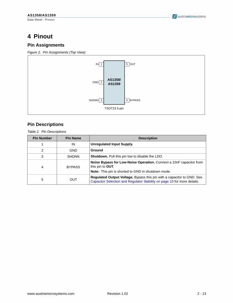
4 PinoutPin AssignmentsFigure 2. Pin Assignments (Top View)
Pin DescriptionsTable 2. Pin Descriptions
Pin Number Pin Name Description
1 IN Unregulated Input Supply.
2 GND Ground
3 SHDNN Shutdown. Pull this pin low to disable the LDO.
4 BYPASSNoise Bypass for Low-Noise Operation. Connect a 10nF capacitor from this pin to OUT. Note: This pin is shorted to GND in shutdown mode.
5 OUT Regulated Output Voltage. Bypass this pin with a capacitor to GND. See Capacitor Selection and Regulator Stability on page 10 for more details.
3SHDNN
2GND
1IN
4 BYPASS
5 OUT
TSOT23 5-pin
AS1358/AS1359
www.austriamicrosystems.com Revision 1.02 2 - 13
AS1358/AS1359Data Sheet - Abso lu te Max imum Rat ings
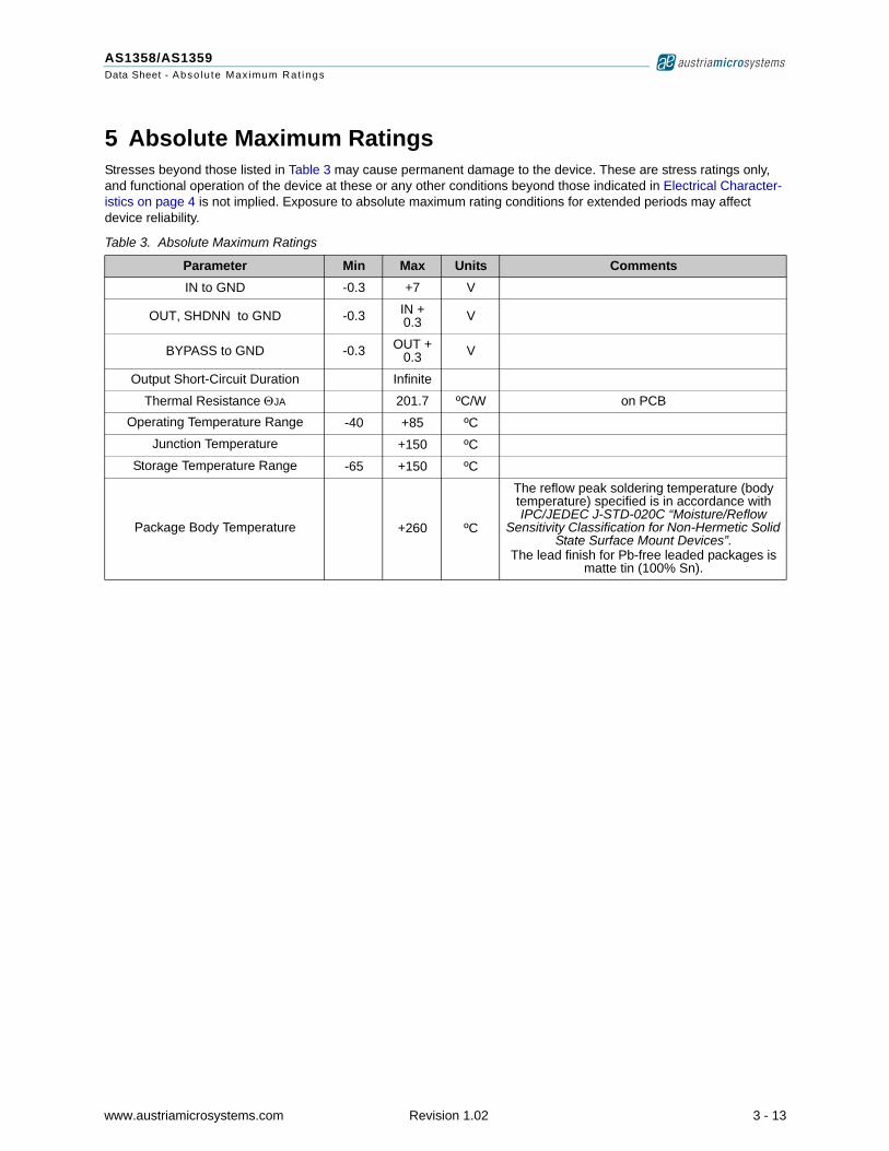
5 Absolute Maximum RatingsStresses beyond those listed in Table 3 may cause permanent damage to the device. These are stress ratings only, and functional operation of the device at these or any other conditions beyond those indicated in Electrical Character-istics on page 4 is not implied. Exposure to absolute maximum rating conditions for extended periods may affect device reliability.
Table 3. Absolute Maximum Ratings
Parameter Min Max Units CommentsIN to GND -0.3 +7 V
OUT, SHDNN to GND -0.3 IN +0.3 V
BYPASS to GND -0.3 OUT +0.3 V
Output Short-Circuit Duration Infinite
Thermal Resistance ΘJA 201.7 ºC/W on PCBOperating Temperature Range -40 +85 ºC
Junction Temperature +150 ºCStorage Temperature Range -65 +150 ºC
Package Body Temperature +260 ºC
The reflow peak soldering temperature (body temperature) specified is in accordance with IPC/JEDEC J-STD-020C “Moisture/Reflow
Sensitivity Classification for Non-Hermetic Solid State Surface Mount Devices”.
The lead finish for Pb-free leaded packages is matte tin (100% Sn).
www.austriamicrosystems.com Revision 1.02 3 - 13
AS1358/AS1359Data Sheet - E lec t r i ca l Charac te r i s t i cs
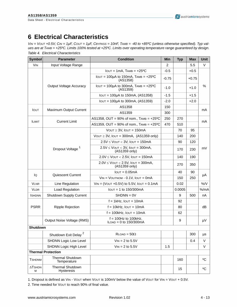
6 Electrical CharacteristicsVIN = VOUT +0.5V, CIN = 1µF, COUT = 1µF, CBYPASS = 10nF, TAMB = -40 to +85ºC (unless otherwise specified). Typ val-ues are at TAMB = +25ºC. Limits 100% tested at +25ºC. Limits over operating temperature range guaranteed by design.Table 4. Electrical Characteristics
Symbol Parameter Condition Min Typ Max UnitVIN Input Voltage Range 2 5.5 V
Output Voltage Accuracy
IOUT = 1mA, TAMB = +25ºC -0.5 +0.5
%
IOUT = 100µA to 150mA, TAMB = +25ºC (AS1358) -0.75 +0.75
IOUT = 100µA to 300mA, TAMB = +25ºC (AS1359) -1.0 +1.0
IOUT = 100µA to 150mA, (AS1358) -1.5 +1.5
IOUT = 100µA to 300mA, (AS1359) -2.0 +2.0
IOUT Maximum Output CurrentAS1358 150
mAAS1359 300
ILIMIT Current LimitAS1358, OUT = 90% of nom., TAMB = +25ºC 250 270
mAAS1359, OUT = 90% of nom., TAMB = +25ºC 470 510
Dropout Voltage 1
1. Dropout is defined as VIN - VOUT when VOUT is 100mV below the value of VOUT for VIN = VOUT + 0.5V.
VOUT ≥ 3V, IOUT = 150mA 70 95
mV
VOUT ≥ 3V, IOUT = 300mA, (AS1359 only) 140 200
2.5V ≤ VOUT < 3V, IOUT = 150mA 90 120
2.5V ≤ VOUT < 3V, IOUT = 300mA,(AS1359 only) 170 230
2.0V ≤ VOUT < 2.5V, IOUT = 150mA 140 190
2.0V ≤ VOUT < 2.5V, IOUT = 300mA,(AS1359 only) 270 350
IQ Quiescent CurrentIOUT = 0.05mA 40 90
µAVIN = VOUTNOM - 0.1V, IOUT = 0mA 150 250
VLNR Line Regulation VIN = (VOUT +0.5V) to 5.5V, IOUT = 0.1mA 0.02 %/V
VLDR Load Regulation IOUT = 1 to 150/300mA 0.0005 %/mA
ISHDNN Shutdown Supply Current SHDNN = 0V 9 500 nA
PSRR Ripple Rejection
f = 1kHz, IOUT = 10mA 92
dBf = 10kHz, IOUT = 10mA 80
f = 100kHz, IOUT = 10mA 62
Output Noise Voltage (RMS) f = 100Hz to 100kHz,ILOAD = 0 to 150/300mA 9 µV
Shutdown
Shutdown Exit Delay 2
2. Time needed for VOUT to reach 90% of final value.
RLOAD = 50Ω 300 µs
SHDNN Logic Low Level VIN = 2 to 5.5V 0.4 V
SHDNN Logic High Level VIN = 2 to 5.5V 1.5 VThermal Protection
TSHDNM Thermal Shutdown Temperature 160 ºC
ΔTSHDNM
Thermal Shutdown Hysteresis 15 ºC
www.austriamicrosystems.com Revision 1.02 4 - 13
AS1358/AS1359Data Sheet - Typ ica l Opera t ing Charac te r is t i cs
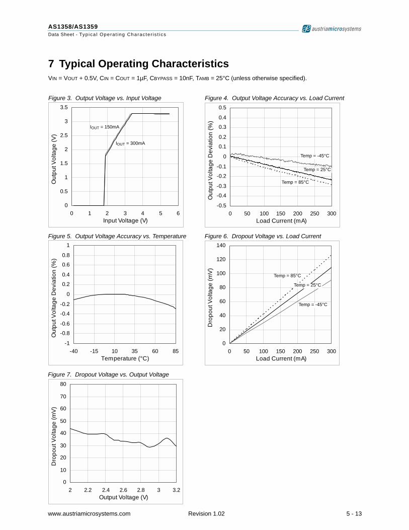
7 Typical Operating CharacteristicsVIN = VOUT + 0.5V, CIN = COUT = 1µF, CBYPASS = 10nF, TAMB = 25°C (unless otherwise specified).
Figure 3. Output Voltage vs. Input Voltage Figure 4. Output Voltage Accuracy vs. Load Current
0
0.5
1
1.5
2
2.5
3
3.5
0 1 2 3 4 5 6Input Voltage (V)
Out
put V
olta
ge (V
) .
IOUT = 300mA
IOUT = 150mA
-0.5
-0.4
-0.3
-0.2
-0.1
0
0.1
0.2
0.3
0.4
0.5
0 50 100 150 200 250 300Load Current (mA)
Out
put V
olta
ge D
evia
tion
(%)
.
Temp = 85°C
Temp = 25°C
Temp = -45°C
Figure 5. Output Voltage Accuracy vs. Temperature Figure 6. Dropout Voltage vs. Load Current
-1
-0.8
-0.6
-0.4
-0.2
0
0.2
0.4
0.6
0.8
1
-40 -15 10 35 60 85Temperature (°C)
Out
put V
olta
ge D
evia
tion
(%)
.
0
20
40
60
80
100
120
140
0 50 100 150 200 250 300Load Current (mA)
Dro
pout
Vol
tage
(mV
) .
Temp = 85°C
Temp = 25°C
Temp = -45°C
Figure 7. Dropout Voltage vs. Output Voltage
0
10
20
30
40
50
60
70
80
2 2.2 2.4 2.6 2.8 3 3.2Output Voltage (V)
Dro
pout
Vol
tage
(mV
) .
www.austriamicrosystems.com Revision 1.02 5 - 13
AS1358/AS1359Data Sheet - Typ ica l Opera t ing Charac te r is t i cs
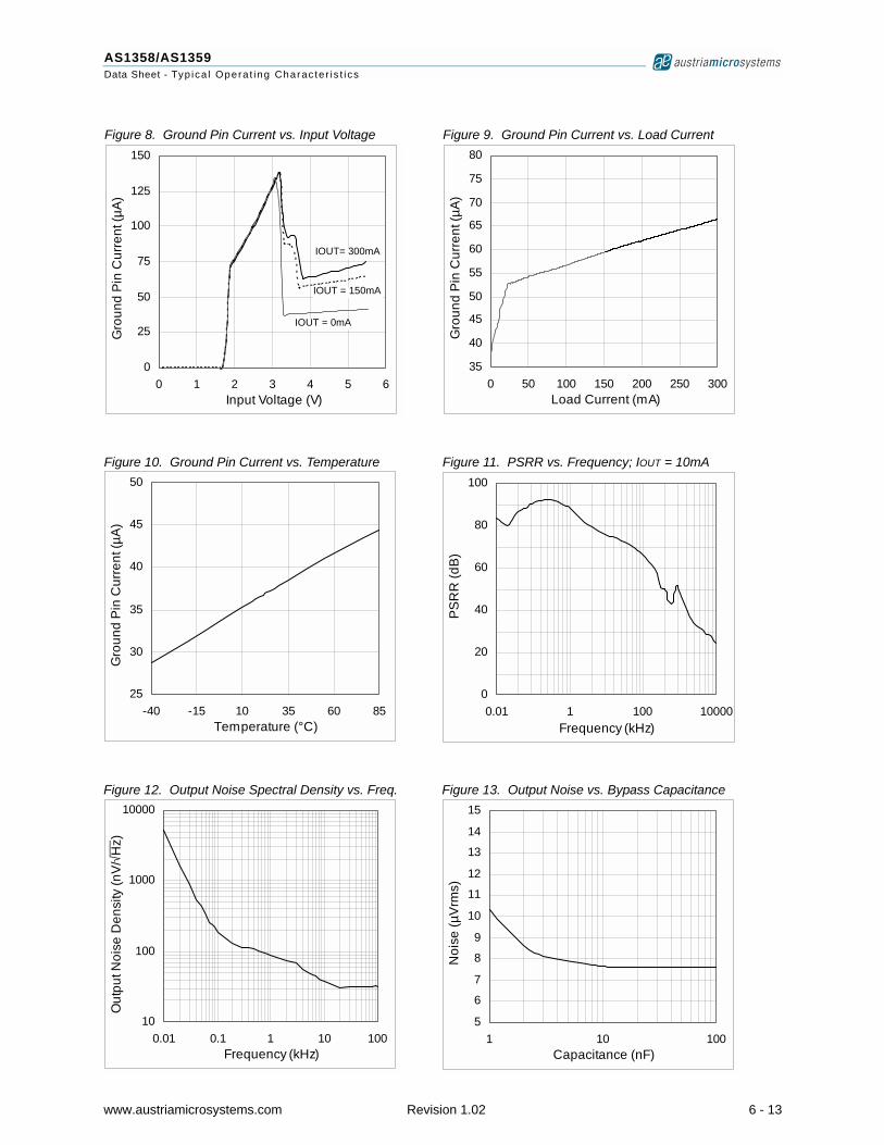
Figure 8. Ground Pin Current vs. Input Voltage Figure 9. Ground Pin Current vs. Load Current
0
25
50
75
100
125
150
0 1 2 3 4 5 6Input Voltage (V)
Gro
und
Pin
Cur
rent
(µA)
.
IOUT = 0mA
IOUT= 300mA
IOUT = 150mA
35
40
45
50
55
60
65
70
75
80
0 50 100 150 200 250 300Load Current (mA)
Gro
und
Pin
Cur
rent
(µA)
.
Figure 10. Ground Pin Current vs. Temperature Figure 11. PSRR vs. Frequency; IOUT = 10mA
25
30
35
40
45
50
-40 -15 10 35 60 85Temperature (°C)
Gro
und
Pin
Cur
rent
(µA)
.
0
20
40
60
80
100
0.01 1 100 10000Frequency (kHz)
PS
RR
(dB
)
Figure 12. Output Noise Spectral Density vs. Freq. Figure 13. Output Noise vs. Bypass Capacitance
10
100
1000
10000
0.01 0.1 1 10 100Frequency (kHz)
Out
put N
oise
Den
sity
(nV/
Hz)
.
5
6
7
8
9
10
11
12
13
14
15
1 10 100Capacitance (nF)
Noi
se (µ
Vrm
s)
.
www.austriamicrosystems.com Revision 1.02 6 - 13
AS1358/AS1359Data Sheet - Typ ica l Opera t ing Charac te r is t i cs
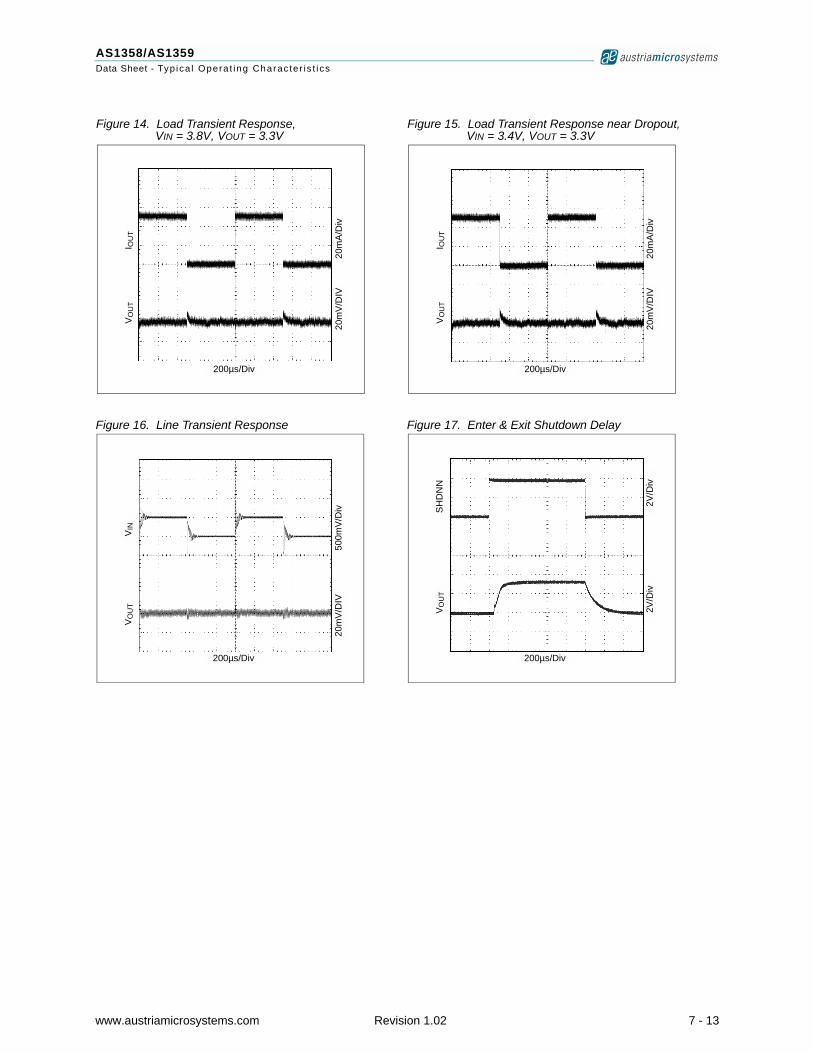
Figure 14. Load Transient Response, VIN = 3.8V, VOUT = 3.3V
Figure 15. Load Transient Response near Dropout, VIN = 3.4V, VOUT = 3.3V
200µs/Div
VO
UT
I OU
T
20m
V/D
IV20
mA
/Div
200µs/Div
VO
UT
I OU
T
20m
V/D
IV20
mA
/Div
Figure 16. Line Transient Response Figure 17. Enter & Exit Shutdown Delay
200µs/Div
V OU
T
20m
V/D
IV50
0mV/
Div
VIN
200µs/Div 2V
/Div
V OU
TS
HD
NN
2V/D
iv
www.austriamicrosystems.com Revision 1.02 7 - 13
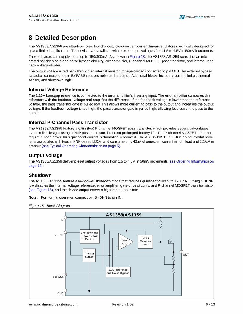
AS1358/AS1359Data Sheet - Deta i led Descr ip t ion
8 Detailed DescriptionThe AS1358/AS1359 are ultra-low-noise, low-dropout, low-quiescent current linear-regulators specifically designed for space-limited applications. The devices are available with preset output voltages from 1.5 to 4.5V in 50mV increments.
These devices can supply loads up to 150/300mA. As shown in Figure 18, the AS1358/AS1359 consist of an inte-grated bandgap core and noise bypass circuitry, error amplifier, P-channel MOSFET pass transistor, and internal feed-back voltage-divider.
The output voltage is fed back through an internal resistor voltage-divider connected to pin OUT. An external bypass capacitor connected to pin BYPASS reduces noise at the output. Additional blocks include a current limiter, thermal sensor, and shutdown logic.
Internal Voltage ReferenceThe 1.25V bandgap reference is connected to the error amplifier’s inverting input. The error amplifier compares this reference with the feedback voltage and amplifies the difference. If the feedback voltage is lower than the reference voltage, the pass-transistor gate is pulled low. This allows more current to pass to the output and increases the output voltage. If the feedback voltage is too high, the pass transistor gate is pulled high, allowing less current to pass to the output.
Internal P-Channel Pass TransistorThe AS1358/AS1359 feature a 0.5Ω (typ) P-channel MOSFET pass transistor, which provides several advantages over similar designs using a PNP pass transistor, including prolonged battery life. The P-channel MOSFET does not require a base driver, thus quiescent current is dramatically reduced. The AS1358/AS1359 LDOs do not exhibit prob-lems associated with typical PNP-based LDOs, and consume only 40µA of quiescent current in light load and 220µA in dropout (see Typical Operating Characteristics on page 5).
Output VoltageThe AS1358/AS1359 deliver preset output voltages from 1.5 to 4.5V, in 50mV increments (see Ordering Information on page 12).
ShutdownThe AS1358/AS1359 feature a low-power shutdown mode that reduces quiescent current to <200nA. Driving SHDNN low disables the internal voltage reference, error amplifier, gate-drive circuitry, and P-channel MOSFET pass transistor (see Figure 18), and the device output enters a high-impedance state.
Note: For normal operation connect pin SHDNN to pin IN.
Figure 18. Block Diagram
AS1358/AS1359
Shutdown and Power-Down
Control
ThermalSensor
OUT
IN
SHDNN
GND
BYPASS
-
+
MOS Driver w/
ILIMIT
ErrorAmp
1.25 Referenceand Noise Bypass
www.austriamicrosystems.com Revision 1.02 8 - 13
AS1358/AS1359Data Sheet - Deta i led Descr ip t ion
Current LimitThe AS1358/AS1359 include a current limiting circuitry to monitor and control the P-channel MOSFET pass transis-tor’s gate voltage, thus limiting the device output current to 270mA (AS1358) and 510mA (AS1359).
Note: See Table 4 on page 4 for the recommended min and max current limits. The output can be shorted to ground indefinitely without causing damage to the device.
Thermal ProtectionIntegrated thermal protection circuitry limits total power dissipation in the AS1358/AS1359. When the junction temper-ature (TJ) exceeds +160ºC, the thermal sensor signals the shutdown logic, turning off the P-channel MOSFET pass transistor and allowing the device to cool down. The thermal sensor turns the pass transistor on again after the device’s junction temperature drops by 10ºC, resulting in a pulsed output during continuous thermal-overload condi-tions.
Note: Thermal protection is designed to protect the devices in the event of fault conditions. For continuous operation, do not exceed the absolute maximum junction temperature rating of +150ºC.
Operating Region and Power DissipationThe AS1358/AS1359 maximum power dissipation is dependant on the thermal resistance of the case and PCB, the temperature difference between the die junction and TAMB, and airflow rate. Power dissipation across the device is calculated as:
PD = IOUT (VIN - VOUT) (EQ 1)The maximum power dissipation is calculated:
PDMAX = (TJ - TAMB)/(θJC + θCA) (EQ 2)Where:TJ - TAMB is the temperature difference between the AS1358/AS1359 die junction and the surrounding air;θJC is the thermal resistance of the package;θCA is the thermal resistance through the PC board/copper traces/other materials to the surrounding air.
Note: Pin GND of the AS1358/AS1359 provides the electrical connection to system ground and also serves as a heat sink. Connect pin GND to the system ground using a large pad or ground plane.
Noise ReductionThe AS1358/AS1359 noise bypass circuitry dramatically reduces output noise, exhibiting 9µVRMS of output voltage noise with CBYPASS = 0.01µF and COUT = 1µF. Use an external 0.01µF bypass capacitor between pin BYPASS and pin OUT (see Figure 1 on page 1).
Note: Startup time is minimized by internal power-on circuitry which pre-charges CBYPASS.
www.austriamicrosystems.com Revision 1.02 9 - 13
AS1358/AS1359Data Sheet - App l ica t ion In fo rmat ion
9 Application InformationCapacitor Selection and Regulator StabilityFor normal operation, use a 1µF capacitor at pin IN and a 1µF capacitor at pin OUT. Larger input capacitor values and lower ESR provide better noise rejection and line-transient response. Reduce output noise and improve load-transient response, stability, and power-supply rejection by using large output capacitors.
Note: Some ceramic dielectrics exhibit large capacitance and ESR variation with temperature. With dielectrics such as Z5U and Y5V, it may be necessary to use a 2.2µF or larger output capacitor to ensure stability at tempera-tures below -10°C. With X7R or X5R dielectrics, 1µF is sufficient at all operating temperatures.
Bypass CapacitorUse a 0.01µF bypass capacitor at pin BYPASS for low-output voltage noise reduction. The leakage current going into pin BYPASS should be less than 10nA. Increasing the capacitance slightly decreases the output noise. Values above 0.1µF and below 0.001µF are not recommended.
Noise, PSRR, and Transient ResponseThe AS1358/AS1359 are designed to deliver ultra-low noise and high PSRR, as well as low dropout and low quiescent currents in battery-powered systems. The power-supply rejection is 92dB at 1kHz and 62dB at 100kHz. (see PSRR vs. Frequency; IOUT = 10mA on page 6).
When operating from sources other than batteries, improved supply-noise rejection and transient response can be achieved by increasing the values of the input and output capacitors, and through passive filtering techniques.
The Figure 16 and Figure 14 on page 7 show the AS1358/AS1359 line- and load-transient responses.
Dropout VoltageThe AS1358/AS1359 minimum dropout voltage determines the lowest usable supply voltage. In battery-powered sys-tems, this determines the useful end-of-life battery voltage.
Since the AS1358/AS1359 use a P-channel MOSFET pass transistor, the dropout voltage is a function of drain-to-source on-resistance (RDS(ON)) multiplied by ILOAD (see Figure 6 on page 5).
www.austriamicrosystems.com Revision 1.02 10 - 13
AS1358/AS1359Data Sheet - Package Drawings and Mark ings
10 Package Drawings and MarkingsThe devices are available in a TSOT23 5-pin package.
Figure 19. TSOT23 5-pin Package
Notes:1. Dimensioning and tolerancing conform to ASME Y14.5M - 1994.2. Dimensions are in millimeters.3. Dimension D does not include mold flash, protrusions, or gate burrs. Mold flash, protrusions, and gate burrs shall
not exceed 0.15mm per end. Dimension E1 does not include interlead flash or protrusion. Interlead flash or pro-trusion shall not exceed 0.15mm per side. Dimensions D and E1 are determined at datum H.
4. The package top can be smaller than the package bottom. Dimensions D and E1 are determined at the outer-most extremes of the plastic body exclusive of mold flash, tie bar burrs, gate burrs, and interlead flash, but include any mistmatches between the top of the package body and the bottom. D and E1 are determined at datum H.
Symbol Min Typ Max Notes Symbol Min Typ Max NotesA 1.00 L 0.30 0.40 0.50
A1 0.01 0.05 0.10 L1 0.60REFA2 0.84 0.87 0.90 L2 0.25BSCb 0.30 0.45 N 5b1 0.31 0.35 0.39 R 0.10c 0.12 0.15 0.20 R1 0.10 0.25
c1 0.08 0.13 0.16 θ 0º 4º 8º
D 2.90BSC 3,4 θ1 4º 10º 12ºE 2.80BSC 3,4 Tolerances of Form and Position
E1 1.60BSC 3,4 aaa 0.15e 0.95BSC bbb 0.25e1 1.90BSC ccc 0.10
ddd 0.20
www.austriamicrosystems.com Revision 1.02 11 - 13

AS1358/AS1359Data Sheet - Order ing In fo rmat ion
11 Ordering InformationThe devices are available as the standard products shown in Table 5.
All devices are RoHS compliant and free of halogene substances.
Non-standard devices from 1.5 to 4.5V are available in 50mV steps. For more information and inquiries contacthttp://www.austriamicrosystems.com/contact
Table 5. Ordering Information
Model Marking Output Current Output Voltage Delivery Form PackageAS1358-BTTT-15 ASLI 150mA 1.5V Tape and Reel TSOT23 5-pin
AS1358-BTTT-18 ASLJ 150mA 1.8V Tape and Reel TSOT23 5-pin
AS1358-BTTT-25 ASLK 150mA 2.5V Tape and Reel TSOT23 5-pin
AS1358-BTTT-26 ASLL 150mA 2.6V Tape and Reel TSOT23 5-pin
AS1358-BTTT-27 ASLM 150mA 2.7V Tape and Reel TSOT23 5-pin
AS1358-BTTT-28 ASLN 150mA 2.8V Tape and Reel TSOT23 5-pin
AS1358-BTTT-285 ASLO 150mA 2.85V Tape and Reel TSOT23 5-pin
AS1358-BTTT-30 ASLP 150mA 3.0V Tape and Reel TSOT23 5-pin
AS1358-BTTT-33 ASLQ 150mA 3.3V Tape and Reel TSOT23 5-pin
AS1358-BTTT-45 ASLR 150mA 4.5V Tape and Reel TSOT23 5-pin
AS1359-BTTT-15 ASLS 300mA 1.5V Tape and Reel TSOT23 5-pin
AS1359-BTTT-18 ASLT 300mA 1.8V Tape and Reel TSOT23 5-pin
AS1359-BTTT-25 ASLU 300mA 2.5V Tape and Reel TSOT23 5-pin
AS1359-BTTT-26 ASLV 300mA 2.6V Tape and Reel TSOT23 5-pin
AS1359-BTTT-27 ASLW 300mA 2.7V Tape and Reel TSOT23 5-pin
AS1359-BTTT-28 ASLX 300mA 2.8V Tape and Reel TSOT23 5-pin
AS1359-BTTT-285 ASLY 300mA 2.85V Tape and Reel TSOT23 5-pin
AS1359-BTTT-30 ASLZ 300mA 3.0V Tape and Reel TSOT23 5-pin
AS1359-BTTT-33 ASL0 300mA 3.3V Tape and Reel TSOT23 5-pin
AS1359-BTTT-45 ASL1 300mA 4.5V Tape and Reel TSOT23 5-pin
www.austriamicrosystems.com Revision 1.02 12 - 13
AS1358/AS1359Data Sheet
CopyrightsCopyright © 1997-2009, austriamicrosystems AG, Schloss Premstaetten, 8141 Unterpremstaetten, Austria-Europe. Trademarks Registered ®. All rights reserved. The material herein may not be reproduced, adapted, merged, translated, stored, or used without the prior written consent of the copyright owner.
All products and companies mentioned are trademarks or registered trademarks of their respective companies.
DisclaimerDevices sold by austriamicrosystems AG are covered by the warranty and patent indemnification provisions appearing in its Term of Sale. austriamicrosystems AG makes no warranty, express, statutory, implied, or by description regarding the information set forth herein or regarding the freedom of the described devices from patent infringement. austriamicrosystems AG reserves the right to change specifications and prices at any time and without notice. Therefore, prior to designing this product into a system, it is necessary to check with austriamicrosystems AG for current information. This product is intended for use in normal commercial applications. Applications requiring extended temperature range, unusual environmental requirements, or high reliability applications, such as military, medical life-support or life-sustaining equipment are specifically not recommended without additional processing by austriamicrosystems AG for each application. For shipments of less than 100 parts the manufacturing flow might show deviations from the standard production flow, such as test flow or test location.
The information furnished here by austriamicrosystems AG is believed to be correct and accurate. However, austriamicrosystems AG shall not be liable to recipient or any third party for any damages, including but not limited to personal injury, property damage, loss of profits, loss of use, interruption of business or indirect, special, incidental or consequential damages, of any kind, in connection with or arising out of the furnishing, performance or use of the technical data herein. No obligation or liability to recipient or any third party shall arise or flow out of austriamicrosystems AG rendering of technical or other services.
Contact InformationHeadquartersaustriamicrosystems AGA-8141 Schloss Premstaetten, Austria
Tel: +43 (0) 3136 500 0Fax: +43 (0) 3136 525 01
For Sales Offices, Distributors and Representatives, please visit:
http://www.austriamicrosystems.com/contact-us
www.austriamicrosystems.com Revision 1.02 13 - 13
Top Related