


Languages
Pages
Legal


Analog Electronics
Module 1: Semiconductor Diodes
PREPARED BY
Academic Services Unit
August 2011
© Applied Technology High Schools, 2011

ATE1210 – Analog Electronics
Module 1: Semiconductor Diode 2
Module 1: Semiconductor Diodes
Module Objectives Upon successful completion of this module, students should be able to:
1. Identify the purpose of the diode and give a brief description of its construction.
2. Sketch the schematic symbol of a diode. 3. Identify the diode by its number code or package type. 4. Distinguish between the terminals of a diode. 5. Recognize whether a diode is forward biased or reverse biased by
observing the voltage polarity. 6. Explain how the diode functions in the forward or reverse bias direction. 7. Test a diode and check its condition. 8. Explain the operation of a half-wave rectifier. 9. Explaing the operation of a full-wave bridge rectifier. 10. Build half-wave and full-wave rectifier circuits and test their functioning.
Module Contents:
Topic Page No.
1.1 Introduction 3
1.2 Diode identification 5
1.3 Diode Operation 6
1.4 Testing a Diode 7
1.5 Diode Application 9
1.6 Lab Activity 1 13
1.7 Lab Activity 2 17
1.8 Lab Activity 3 20
1.9 Review Exercise 23

ATE1210 – Analog Electronics
Module 1: Semiconductor Diode 3
1.1 INTRODUCTION
The invention of semiconductor devices was a revolution, which lead to an
impressive technological achievement that would endlessly alter modern
society. Semiconductor devices, made electronics physically very small,
including computers, certain types of medical diagnostic and treatment
equipment, and popular telecommunication devices. A diode is a
semiconductor device that allows current to flow in only one direction.
A semiconductor in its pure form does not conduct current well because it
has limited number of free electrons and holes. Doping is the process of
increasing the conductivity of the semiconductor where in small amounts of
impurities are added to a pure semiconductor. An N-type semiconductor has
more number of electrons (negative charges) and a P-type semiconductor
has more number of holes (positive charges). Sandwiching, or joining a P-
type semiconductor with N-type semiconductor forms a diode. The diode is
contained in a small capsule made of glass or plastic and has two terminals
or electrodes and hence the name diode (di two and ode electrode). The
electrode connected to the P-type is called the Anode “A”, and the electrode
connected to the N-type is called the Cathode “K”. The cathode (K) is
marked with a silver color band as shown in Figure 1(c). Figure 1(a) and
1(b) shows the structure and symbol of the PN junction diode.
K
b) Diode Symbol
A
Anode
(A) Cathode
(K) N-TYPE
Electrons
+
a) Diode Structure
P-TYPE
Holes
c) Typical Diode
Cathode (K)
Figure 1: Diode structure and Symbol

ATE1210 – Analog Electronics
Module 1: Semiconductor Diode 4
Diode Types
According to the type of semiconductors they are classified into:
Germanium diodes
Silicon diodes
According to their application, they are classified into the following:
Rectifier diodes. Zener diodes.
Light emitting diodes (LEDs). Photo diodes.
Figure 2 shows commonly used diodes of different types.
Photo DiodeZener Diode
Low Power Diode
Rectifier diode
LED
Figure 2 Typical Diodes of different types
Diode Packing
Diode is generally mounted in one of three basic packages shown in figure
3. These are designed to protect the diode from mechanical stress and the
environment. The size of the package indicates the current rating (larger
size means higher current rating). Note that (DO) refers to Diode Outline.
DO-5
Figure 3 Diode packing types
DO-8 DO-41

ATE1210 – Analog Electronics
Module 1: Semiconductor Diode 5
1.2 Diode Identification There are hundreds of diodes, of different types and characteristics
according to the way they are designed and made. In order to distinguish
between them, each type is given a unique code so that it can be identified.
In fact there are two main semiconductor numbering systems in use:
1) Pro-Electron System: This numbering system originated in Europe
and is widely used for semiconductors developed and manufactured by
them.
2) JEDEC System: This numbering system originated in the USA and is
widely used for semiconductors manufactured in North America.
1.1 Pro-Electron Numbering or Coding System
First Letter Specifies Semiconductor Material
Second Letter Specifies type of Diode
A Germanium A Low power or signal
B Silicon P Light detector
Q Light Emitting Diode (LED)
Y Rectifier
EXAMPLE: BZY74-C6V3
B = Si, Z = Zener diode, Y74 = Commercial or
Industrial use, C = 5% of rating voltage.
6V3 = 6.3 Volt (Voltage rating) Z Zener (voltage reference)
1.2 JEDEC Numbering or Coding System
First Number Second Letter Subsequent numbers
1 Diode N Semiconductor Serial number of device
2 Bipolar Transistor
3 FET
4&5 Photo Coupler
Example: This code “1N4001” means:
1 Diode, N Semiconductor.
4001 Serial number.
ATE1210 – Analog Electronics
Module 1: Semiconductor Diode 6
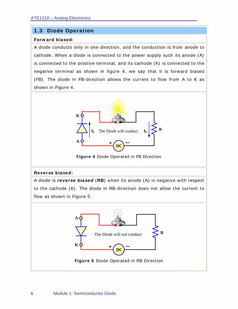
1.3 Diode Operation
Forward biased:
A diode conducts only in one direction, and the conduction is from anode to
cathode. When a diode is connected to the power supply such its anode (A)
is connected to the positive terminal, and its cathode (K) is connected to the
negative terminal as shown in figure 4, we say that it is forward biased
(FB). The diode in FB-direction allows the current to flow from A to K as
shown in Figure 4.
Figure 4 Diode Operated in FB Direction
DC+
RThe Diode will conduct IF IF
K
A
Reverse biased:
A diode is reverse biased (RB) when its anode (A) is negative with respect
to the cathode (K). The diode in RB-direction does not allow the current to
flow as shown in Figure 5.
Figure 5 Diode Operated in RB Direction
DC+
RThe Diode will not conduct
K
A

ATE1210 – Analog Electronics
Module 1: Semiconductor Diode 7
1.4 Testing a Diode
Testing the diode in forward direction with an Ohmmeter:
Connect the positive meter-lead (Red) to the anode (A) and connect the
negative meter-lead (Black) to the cathode (K) as shown in Figure 6a. A
good diode must display low resistance (typically < 10) in FB. Note that
the ohmmeter consists of an internal battery (1.5 V), which can FB or RB a
diode.
Figure 6a Testing the Diode in FB Direction
IN 4001
(A) Anode
(K) Cathode
Ohm
met
er
Testing the diode in reverse direction with an Ohmmeter:
Connect the positive meter-lead (Red) to the cathode (K), and the negative
meter-lead (Black) to the anode (A) as shown in Figure 6b. A good diode
must display a very high resistance (>1000 M) in RB. If both bias
conditions display low resistance, then the diode is shorted, and if both bias
conditions display very high resistance, then the diode is considered to be
open.
Figure 6b Testing the Diode in RB Direction
IN 4001
(A) Anode
(K) Cathode
Ohm
met
er

ATE1210 – Analog Electronics
Module 1: Semiconductor Diode 8
Testing the diode in forward direction with a Digital Multimeter:
Set the digital Multimeter knob to ‘diode testing’ function. Now, connect the
positive lead (Red) to the anode (A) and the negative lead (Black) to the
cathode (K) as shown in Figure 7a. For a diode in a good condition the
reading will be in the range of 0.3V for Ge and 0.7V for Si.
Dig
ital M
ultim
eter
Figure 7a Testing the Diode in FB Direction
IN 4001
(A) Anode
(K) Cathode
Testing the diode in reverse direction with a Digital Multimeter:
Connect the positive lead to the cathode and negative lead to the anode as
shown in Figure 7b. For a diode in good condition, the reading will be 1.5V
for both types. If in both cases the reading is 0V, then the PN junction is
shorted, and if it is 1.5V the PN junction is open.
IN 4001
(A) Anode
(K) Cathode
Dig
ital
Mul
tim
eter
Figure 7b Testing the Diode in RB Direction

ATE1210 – Analog Electronics
Module 1: Semiconductor Diode 9
1.5 Diode Application
The diode has a unique ability to offer very little resistance to current flow in
the forward-bias direction, but maximum resistance to current flow when
reverse biased. For this reason, the diodes are used in rectification.
Rectification is the process of converting ac to pulsating dc, and the diodes
used for this purpose are called rectifier diodes.
AC current behavior:
During the positive alteration, AC current flows first in one direction,
reaches the maximum (positive) and decreases to zero.
During the negative alteration, the current follows the same manner in
the opposite direction.
In each alteration, AC current reverses its direction as shown in Figure 8.
-ve
I
+ve
-ve
+ve
I
Positive half-cycle
Negative half-cycle
Figure 8 Alteration of AC current between (+ve) and (-ve)
Half Wave Rectifier
The half-wave rectifier circuit is constructed simply by connecting a diode
between the secondary of a transformer and the load as shown in Figure 9.
Figure 9 Half Wave Rectifier Circuit
IF A
Load AC
K

ATE1210 – Analog Electronics
Module 1: Semiconductor Diode 10
During the positive half-cycle, the diode conducts when the input voltage
exceeds the barrier potential (0.7V for Silicon and 0.3V for Germanium
diodes) and current flows through the load and returns along the 0V line.
Only the positive half-cycle appears across the load as shown in Figure 10a.
IF A K + +
+ AC Input
Load
Output
Figure 10a Operation during Positive Half-Cycle During the negative half-cycle, the diode turns OFF (RB). This will prevent
any current from flowing, and no voltage appears across the load as shown
in Figure 10b.
IR A K
+ +
+ AC Input
Load
Output
Figure 10b Operation during Negative Half-Cycle
Output Voltage: The net result is that only the positive half-cycles of the AC
input voltage appear across the load, providing a pulsating DC voltage at
the output as shown in Figure 11. However, the amplitude of the output
voltage is less than the input amplitude, and this is because of the forward
voltage drop across the diode. Because this circuit produces output current
only during one cycle, it is called a half-wave rectifier.
Secondary Voltage (VS)
Voltage across the Load
Figure 11 Output of Half-Wave Rectifier Voltage
VRL
VS
Conduct lab activity 1.

ATE1210 – Analog Electronics
Module 1: Semiconductor Diode 11
Full Wave Rectifier
The circuit in figure 12 rectifies AC by using a bridge of four diodes. It is
therefore called a full-wave bridge rectifier.
Figure 12: Bridge Rectifier
During the positive half cycle, diodes D1 and D2 are forward biased, so they
conduct. Diodes D3 and D4 are reverse biased and do not conduct. Current
flows through the load as shown in figure 13.
Figure 13: Conduction during positive half cycle

ATE1210 – Analog Electronics
Module 1: Semiconductor Diode 12
During the negative half cycle as shown in figure 14, diodes D1 and D2 are
reverse biased, so they do not conduct. Diodes D3 and D4 are forward
biased and conduct.
Figure 14: Conduction during negative half cycle
The result is that the current continues to flow through the load in the same
direction in both the half cycles. The output and input are shown in figure
15. The rectifier produces output during both half cycles, and therefore it is
100% efficient. In each half-cycle, current flows through two diodes, and
therefore the output voltage is two voltage drops less than the input
voltage.
Figure 15: Input and Output Waveforms

ATE1210 – Analog Electronics
Module 1: Semiconductor Diode 13
1.6 Lab Activity 1
Objective
To determine the diode polarity and understand the need for proper
connection.
Background Information
A semiconductor diode (or diode) is made from a piece of P-type
semiconductor and a piece of N-type semiconductor joined together as
shown in figure 16.
Figure 16: Diode construction
The amount of current that flows through a diode when it conducts depends
on the size and polarity of the applied voltage. Figure 17(a) shows the diode
symbol, and figure 17(b) shows the types of diodes supplied in the feedback
kit.
Figure 17(a): Diode symbol
Figure 17(b): Diode types

ATE1210 – Analog Electronics
Module 1: Semiconductor Diode 14
Equipment Required
Apparatus Quantity
Electricity & Electronics Constructor, EEC470
1
Basic Electricity and Electronics Kit EEC471-2
1
Power supply unit 0 to 20 V (Feedback Power Supply 92-445)
1
Digital Multimeters 2
Diode (1N4007), R = 4.7k 1-each
Procedure
1. As shown in the patching diagram of figure 18, construct the circuit of
figure 19(a). (Note that the resistor limits the current to a safe value).
Figure 18: Constructor-EEC470
Figure 19(a): Diode’s Circuit diagram

ATE1210 – Analog Electronics
Module 1: Semiconductor Diode 15
2. Move knob of the power supply control to 0V position.
3. Switch on the power supply.
4. Set the power supply control to give 10 V on the meter.
5. Record the current measurement in the first row of the result table figure
20.
6. Now, switch off the power supply.
7. Reverse the 1N4007 diode to give the circuit of figure 19(b).
Figure 19(b): Diode’s Circuit diagram
1. Switch on the power supply and readjust the voltage to 10 V.
2. Read the new value of diode current and record it in the second row of
the result table figure 20.
3. Study your results and answer the questions on the next page.
Observations:
Write your observation in table below.
Circuit Current (mA)
Figure 19(a) IF = ……………….
Figure 19(b) IR = ……………….
Figure 20: Observation Table

ATE1210 – Analog Electronics
Module 1: Semiconductor Diode 16
Questions 1) Which side of a diode should be connected to the positive voltage
supply to make it conduct current?
…………………………………………………………………………………………………………
…………………………………………………………………………………………………………
2) When the diode was connected the opposite way round was the
current?
a) slightly smaller
b) much smaller
c) too small to measure
3) Which side of a diode should be connected to the positive voltage
supply to make it stop current?
…………………………………………………………………………………………………………
…………………………………………………………………………………………………………
Conclusion:
The diode conduct current when the Anode is connected to the
……………………… and the Cathode is connected to the ………………………
The diode does not conduct current when the Anode is connected to
the ………………… and the Cathode is connected to the ………………………

ATE1210 – Analog Electronics
Module 1: Semiconductor Diode 17
1.7 Lab Activity 2
Objectives:
1. To learn to recognize a half-wave rectified sinusoidal voltage.
2. To understand the term ‘mean value’ as applied to a rectified
waveform.
3. To understand the effect of a reservoir capacitor upon the rectified
waveform and its mean value.
Equipment Required
Apparatus Quantity
Electricity & Electronics Constructor, EEC470.
1
Basic Electricity and Electronics Kit EEC471-2.
1
Power supply unit 0 to 20 V (Feedback Power Supply 92-445)
1
Power supply unit. ac supply; 12 V rms; 50 or 60 Hz.
1
Digital Multimeters. 2
Oscilloscope. 1
Diode (SY356/6), R = 10k, and Capacitor. 1-each
Procedure
1. Switch on the oscilloscope and the sinusoidal supply.
2. With the oscilloscope dc coupled adjust the time-base and the Y
amplifier sensitivity to obtain a steady trace of about 4 cm vertical and
5 ms/cm horizontal. You should see a waveform as in figure 21.
Figure 21: Half-wave Rectified Waveform

ATE1210 – Analog Electronics
Module 1: Semiconductor Diode 18
3. As shown in the patching diagram of figure 22, construct the circuit of
figure 23.
Figure 22: Constructor-EEC470
Figure 23: Half-wave Rectification
4. Measure and record the time T and the ge Vpk
5. Sketch the waveform and label it to show the periods when the diode
is conducting and those when it is not.
6. Time T depends upon the frequency of your power supply. For a 50Hz
supply it should be 20 ms and for 60 Hz it should be 17ms.
7. Confirm this: Vpk should be very nearly equal to the peak voltage of
the alternating supply.
ATE1210 – Analog Electronics
Module 1: Semiconductor Diode 19
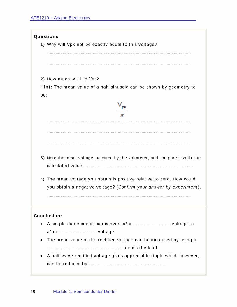
Questions
1) Why will Vpk not be exactly equal to this voltage?
…………………………………………………………………………………………………………
…………………………………………………………………………………………………………
2) How much will it differ?
Hint: The mean value of a half-sinusoid can be shown by geometry to
be:
…………………………………………………………………………………………………………
…………………………………………………………………………………………………………
…………………………………………………………………………………………………………
3) Note the mean voltage indicated by the voltmeter, and compare it with the
calculated value. ……………………………………………………………..………………
4) The mean voltage you obtain is positive relative to zero. How could
you obtain a negative voltage? (Confirm your answer by experiment).
…………………………………………………………………………………………………………
Conclusion:
A simple diode circuit can convert a/an ………………………… voltage to
a/an ……………………………voltage.
The mean value of the rectified voltage can be increased by using a
……………………………………………………… across the load.
A half-wave rectified voltage gives appreciable ripple which however,
can be reduced by ……………………………………………………….

ATE1210 – Analog Electronics
Module 1: Semiconductor Diode 20
1.8 Lab Activity 3
Objective: To understand the working of a diode bridge circuit as a full-wave rectifier
and its advantage over half-wave rectifier.
Equipment Required
Apparatus Quantity
Electricity & Electronics Constructor, EEC470.
1
Basic Electricity and Electronics Kit EEC471-2.
1
Power supply unit 0 to 20 V (Feedback Power Supply 92-445)
1
Power supply unit. ac supply; 12 V rms; 50 or 60 Hz.
1
Digital Multimeters. 2
Oscilloscope. 1
Bridge-Rectifier, R = 10k, and Capacitor. 1-each
Procedure: Select the Bridge Rectifier from the component kit. It appears
as in figure 24(a) and figure 24(b). Note how the rectifier terminals are
labeled.
(a) Bridge Module
(b) Circuit
Figure 24: Bridge Rectifier
1. Note: Prior to connecting an ac power supply to the board, ensure the
supply is isolated from ground.

ATE1210 – Analog Electronics
Module 1: Semiconductor Diode 21
2. With the oscilloscope dc coupled adjust the time-base and the Y
amplifier sensitivity to obtain a steady trace of about 4 cm vertical and
5 ms/cm horizontal. You should see a waveform as in figure 25. Time
'T' will be 10 ms for 50 Hz supply, and 8.5 ms for 60 Hz.
Figure 25: Full-wave Rectified Waveform
3. Construct the circuit of figure 26 as in the patching diagram of figure 25
Figure 25: Constructor-EEC470
Figure 26: Test Circuit (full-wave rectifier)

ATE1210 – Analog Electronics
Module 1: Semiconductor Diode 22
4. Measure and record the time T and the peak voltage Vpk
5. Sketch the waveform and label it to show the periods of each 2-diode.
6. Note the value of Vpk.
7. Note the mean value of output voltage indicated on the voltmeter.
8. Compare these values with those obtained in Lab activity-2.
9. Confirm this: Vpk should be very nearly equal to the peak voltage of
the alternating supply.
Conclusion:
A bridge ……………………… rectifier gives a greater mean value and fewer
ripples for a given load and reservoir capacitor than a ………………………
rectifier.
The alternative full-wave circuit using a centre-tapped transformer and two
diodes is less efficient than the bridge circuit because it requires a bigger
transformer for a given output power.

ATE1210 – Analog Electronics
Module 1: Semiconductor Diode 23
1.9 Review Exercise
1. The cathode of a diode is made 4V positive of its anode.
a) What is the name of this type of bias?
____________________________________________________________________
b) Does current flow through the diode in this case?
____________________________________________________________________
2. Draw a circuit of a half-rectifier, and draw a sketch of 3 cycles of it output waveform.
Circuit Diagram:
Waveforms:

ATE1210 – Analog Electronics
Module 1: Semiconductor Diode 24
3. Draw the output voltage waveform of the rectifier for the indicated input voltage, as shown in the figure below. The 1N4003 is a specific rectifier diode with a barrier potential/forward voltage drop of 0.7V.
4. Draw the bridge rectifier circuit, and sketch 3 cycles of its input and output waveforms.
Circuit Diagram:
Waveforms:

ATE1210 – Analog Electronics
Module 1: Semiconductor Diode 25
Notes
_____________________________________________________________________________ _____________________________________________________________________________ _____________________________________________________________________________ _____________________________________________________________________________ _____________________________________________________________________________ _____________________________________________________________________________ _____________________________________________________________________________ _____________________________________________________________________________ _____________________________________________________________________________ _____________________________________________________________________________ _____________________________________________________________________________ _____________________________________________________________________________ _____________________________________________________________________________ _____________________________________________________________________________ _____________________________________________________________________________ _____________________________________________________________________________ _____________________________________________________________________________ _____________________________________________________________________________ _____________________________________________________________________________ _____________________________________________________________________________ _____________________________________________________________________________ _____________________________________________________________________________ _____________________________________________________________________________

ATE1210 – Analog Electronics
Module 1: Semiconductor Diode 26
Notes
_____________________________________________________________________________ _____________________________________________________________________________ _____________________________________________________________________________ _____________________________________________________________________________ _____________________________________________________________________________ _____________________________________________________________________________ _____________________________________________________________________________ _____________________________________________________________________________ _____________________________________________________________________________ _____________________________________________________________________________ _____________________________________________________________________________ _____________________________________________________________________________ _____________________________________________________________________________ _____________________________________________________________________________ _____________________________________________________________________________ _____________________________________________________________________________ _____________________________________________________________________________ _____________________________________________________________________________ _____________________________________________________________________________ _____________________________________________________________________________ _____________________________________________________________________________ _____________________________________________________________________________ _____________________________________________________________________________
Top Related