


Languages
Pages
Legal


White Paper
An Era of Affordability for the Custom System-on-Chip (SoC)Michele Riga, IoT/Embedded Business, Arm
September, 2019
P2. Introduction
P2. Benefits of a custom SoC
P3. New products are driving down costs
P4. Accessible silicon technology
P5. Building-block IP availability and affordability
P6. Design help
P7. Case study: S3 Semiconductors and the oil and gas
industry P8. Silicon manufacturing options
P9. Beyond silicon: software reuse
P9. Conclusion
2
Now that electronic system design prototypes can be developed for under $20,000, it pays to explore the benefits.
Introduc�tion
The world is on track to design, make, and connect a trillion devices by 2035. It will
be a diverse world of performance and use cases, but there are some universal design
considerations: interoperability, security, scalability, resiliency, and in many cases, autonomy.
There is no doubt that these considerations add complexity and warrant the need for
custom silicon; however, there is also a need to shorten develop cycles and minimize costs.
How can you have both?
Today, for reasons of cost efficiency and getting to market faster, most companies source
secure, cost-efficient frameworks, services, and tools that accelerate development. These
designs come from an expanding and reliable ecosystem of suppliers. Now, there are more
hardware and software options for electronic system design than ever before, and this has
meant that the cost of a custom SoC is increasingly affordable, and the benefits accessible,
regardless of budget or expertise.
This white paper considers the benefits of building custom system-on-chip (SoC), and is
supported by a study of an industrial control application with real-world data on cost, size,
and power consumption.
Benefits of a Custom SoC
There are many potential reasons and benefits of building a custom SoC:
Lowering overall product costs, replacing discrete components with one chip.
Reducing component count, complexity, and PCB size.
Improving reliability – a conventional PCB with hundreds of individual components has many potential failure points, many of which can be removed by limiting component count with custom silicon.
Protecting the product, making it harder, or impossible, to reverse engineer and copy.
Reducing supply chain complexity and assuming complete ownership of the chip, ensuring long life supply using established foundries and process nodes.
Making a product more compelling and differentiated by adding new features not available in standard products.
Meeting performance and/or cost requirements for a specific application or product that are impossible to reach with a PCB approach.

3
Supply chain security is a crucially important factor. Completed silicon wafers, without the
cost of testing and packaging, can be stored securely and then accessed over time. Years
of device supply can then be maintained at lower cost. This contrasts with maintaining a
supply of many discrete components that must be purchased at full price in advance. The
benefits of custom silicon for the purchasing and supply chain team are substantial.
What’s more, thanks to the availability of proven IP, skilled design service companies, and
mature chip manufacturing, designing a custom SoC no longer requires a huge investment.
Prototype test chips can be manufactured for under $20,000, a figure that most OEMs
can easily afford.
New Products are Driving Down CostsThe last few decades have been marked by significant growth in the quantity of digital
devices shipped. The graph below shows the growth in the number of chips shipped by
Arm’s partners in the last 20 years.
Completely new classes of products have been created, such as the first mobile phones,
smartphones, and wearables. At the same time, existing products have evolved,
with vehicles, white goods, and industrial equipment all becoming increasingly digital.
Most low to medium-volume products are built from off-the-shelf semiconductor
components. However, this approach often limits performance, power efficiency and cost-
competitiveness, especially when many of the analog and digital components have to meet
product requirements. Using custom SoCs can overcome these hurdles.
Figure 1: Number of Arm-based chips shipped in the last 20 years.
Years of device supply can be maintained at lower cost.
4
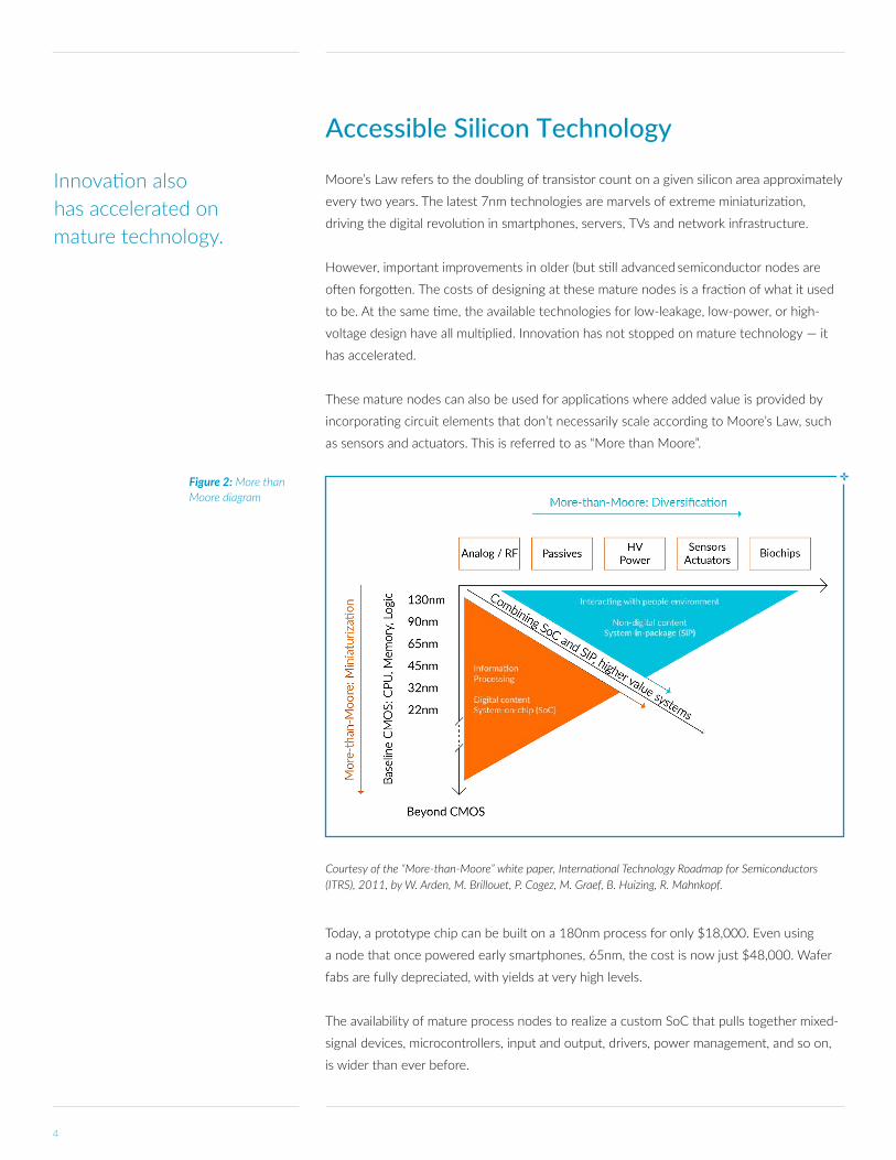
Figure 2: More than Moore diagram
Accessible Silicon Technology
Moore’s Law refers to the doubling of transistor count on a given silicon area approximately
every two years. The latest 7nm technologies are marvels of extreme miniaturization,
driving the digital revolution in smartphones, servers, TVs and network infrastructure.
However, important improvements in older (but still advanced semiconductor nodes are
often forgotten. The costs of designing at these mature nodes is a fraction of what it used
to be. At the same time, the available technologies for low-leakage, low-power, or high-
voltage design have all multiplied. Innovation has not stopped on mature technology — it
has accelerated.
These mature nodes can also be used for applications where added value is provided by
incorporating circuit elements that don’t necessarily scale according to Moore’s Law, such
as sensors and actuators. This is referred to as “More than Moore”.
Courtesy of the “More-than-Moore” white paper, International Technology Roadmap for Semiconductors (ITRS), 2011, by W. Arden, M. Brillouet, P. Cogez, M. Graef, B. Huizing, R. Mahnkopf.
Today, a prototype chip can be built on a 180nm process for only $18,000. Even using
a node that once powered early smartphones, 65nm, the cost is now just $48,000. Wafer
fabs are fully depreciated, with yields at very high levels.
The availability of mature process nodes to realize a custom SoC that pulls together mixed-
signal devices, microcontrollers, input and output, drivers, power management, and so on,
is wider than ever before.
Innovation also has accelerated on mature technology.
5
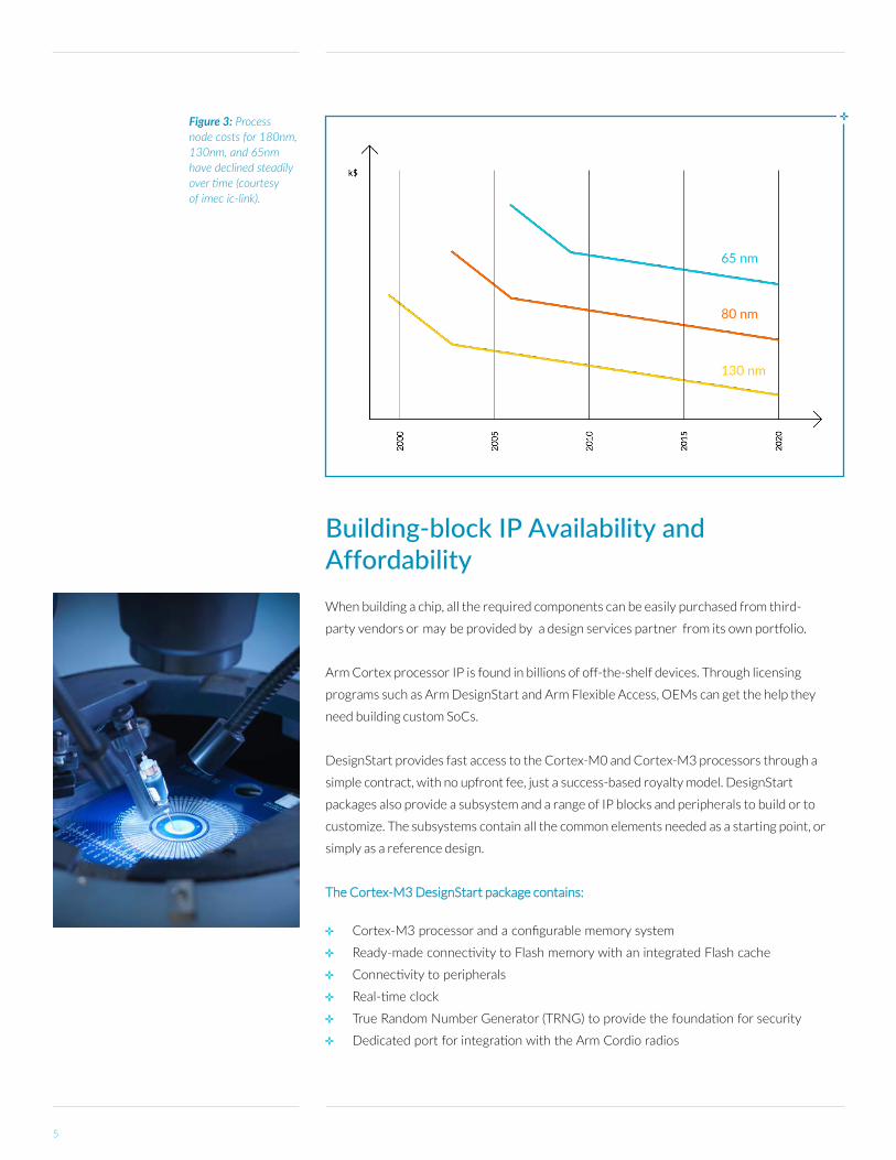
Figure 3: Process node costs for 180nm, 130nm, and 65nm have declined steadily over time (courtesy of imec ic-link).
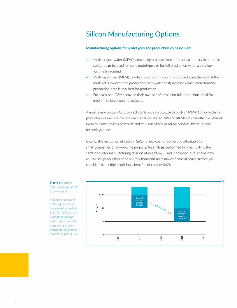
Building-block IP Availability and A�ffordabilityWhen building a chip, all the required components can be easily purchased from third-
party vendors or may be provided by a design services partner from its own portfolio.
Arm Cortex processor IP is found in billions of off-the-shelf devices. Through licensing
programs such as Arm DesignStart and Arm Flexible Access, OEMs can get the help they
need building custom SoCs.
DesignStart provides fast access to the Cortex-M0 and Cortex-M3 processors through a
simple contract, with no upfront fee, just a success-based royalty model. DesignStart
packages also provide a subsystem and a range of IP blocks and peripherals to build or to
customize. The subsystems contain all the common elements needed as a starting point, or
simply as a reference design.
The Cortex-M3 DesignStart package contains:
Cortex-M3 processor and a configurable memory system
Ready-made connectivity to Flash memory with an integrated Flash cache
Connectivity to peripherals
Real-time clock
True Random Number Generator (TRNG) to provide the foundation for security
Dedicated port for integration with the Arm Cordio radios
65 nm
80 nm
130 nm

6
Figure 4: SSE-050 subsystem block diagram
Design Help
Development can be easily outsourced to reputable design service companies. These
companies can assist in all phases of the custom SoC process, enabling OEMs to outsource
any part of the project, from definition to design, integration, verification, and manufacturing.
Some of them can provide a complete turnkey service, delivering a microchip ready to be used.
The Internet of Things (IoT) adds new dimensions to the custom SoC world, as there are
now OEMs and companies looking to create custom silicon with no previous experience.
To help, Arm has established the Approved Design partner program. This program connects
companies with audited design partners, chosen for the quality of the services that they
can provide and with a proven track record of successfully using Arm IP.
Alternatively, Flexible Access provides access to a wider range of IP products, support, tools
and training for unlimited design time and with payment due only at the point of manufacture.
The licensing model includes a wide range of Cortex-A, Cortex-R and Cortex-M CPUs, Mali
GPUs, Corstone foundation IP package, System IP, Security IP and Artisan physical IP
libraries.

7
reduction in power consumption.
70%reduction in
bill-of-materials cost.
80% reduction in
PCB size.
75%
Case Study: S3 Semiconductors and the Oil Gas IndustrySemiconductor design and manufacturing company, S3 Semiconductors, recently developed
a custom SoC for a company in the oil and gas industry. The customer makes complex valve
controllers that sense pressure and temperature. The original controller design was based on
a PCB containing a large variety of off-the-shelf digital and analog parts.
For its next generation product, the customer decided to replace all of its off-the-shelf
parts with one integrated solution. Their motivation was to reduce costs, improve reliability,
and simplify the inventory and supply management. Supply management, in particular,
was a major concern as some of the customer’s vendors were planning to discontinue
components that had been used in the original design. In addition, the company wanted
to add customized functionality with new connectivity to remotely manage valves in the
field. Like most OEMs, the company had no in-house silicon design expertise so they
decided to outsource the project to S3 Semiconductors.
S3 Semiconductors developed a low-power chip based on the 180 nm process node,
integrating digital-to-analog and analog-to-digital converters (DAC and ADC), and
communication interfaces that included I2C, UART, and SPI, all in a low-power design
consuming 160 uW/MHz. The results of the project were:
8
Multi-project wafer (MPW): combining projects from different customers to amortize
costs. It can be used for early prototypes, or for full production when a very low
volume is required.
Multi-layer mask (MLM): combining various masks into one, reducing the cost of the
mask set. However, the production cost (wafer cost) increases since more foundry
production time is required for production.
Full mask-set: OEMs provide their own set of masks for full production. Ideal for
medium to large volume projects.
Almost every custom ASIC project starts with a prototype through an MPW. For low-volume
production, or mid-volume ones with small die size, MPWs and MLMs are cost-effective. Almost
every foundry provides accessible and frequent MPWs or MLMs services, for the various
technology nodes.
Clearly, the realization of custom SoCs is now cost-effective and affordable for
small companies or low-volume projects. An analysis performed by imec IC-link, the
semiconductor manufacturing division of imec’s R&D and innovation hub, shows how
at 180 nm, production of only a few thousand units makes financial sense, before you
consider the multiple additional benefits of custom SoCs.
Silicon Manufacturing Options
Manufacturing options for prototypes and production chips include:
Minimum number of units required for an investment in custom SoC. On 180 nm, with current technology costs, a few thousand units per year are a minimum requirement (courtesy of imec. IC-link).
Figure 5: Custom SoCs can be profitable at low volume.

9
Beyond Silicon: Software ReuseAssembling a chip and manufacturing it is not the end of a custom SoC project. Hardware
has little value unless it’s paired with software that is optimized to run and take full
advantage of all the hardware functions implemented. If software engineers are worried
about the move to a custom part, they can be reassured that developing, debugging and
reusing software remains the same as today. In fact, the same extensive software and
tools ecosystem that enables software developers to easily build software for off-the-shelf
Arm-based MCUs can also be leveraged when transferring to Arm-based custom SoCs.
In addition, companies are using legacy 8 or 16-bit MCUs, then life for software
developers is about to get even better. OEMs using off-the-shelf MCUs or CPUs will find
that moving to a custom SoC, reusing existing software investments and sharing new code
with future projects is far more straightforward than expected.
ConclusionThe barrier to developing chips has dropped significantly and this has led to an explosion in the
number of custom SoCs powering IoT and embedded applications across a wide range of industries
OEMs should consider how a custom SoC can work for them. There is an abundance of
IP available, from proven microprocessors to peripherals and accelerators. Processors,
subsystem IP, tools and models can be accessed in a number of ways, depending on your needs:
• Arm DesignStart provides access to a select mix of IP products and tools with a low upfront
license fee.
• Arm Flexible Access gives SoC design teams access to a wide range of IP products, support,
tools and training for unlimited design time and with payment due only at the point
of manufacture.
These access models provide SoC designers with unlimited flexibility to experiment, evaluate
and design, and ensures overall costs remain proportional to the size of the project.
Start your custom SoC today by exploring the options available for accessing IP with Arm.
Copyright © 2019 Arm Limited. All rights reserved. The Arm logo is a registered trademark of Arm Ltd. All other trademarks are the property of their respective owners and are acknowledged
Top Related