


Languages
Pages
Legal


Computer = H/W + S/W Program(S/W)
A sequence of instruction S/W = Program + Data
The data that are manipulated by the program constitute the data base
Application S/W DB, word processor, Spread Sheet
System S/W OS, Firmware, Compiler, Device
Driver
1-1 Digital Computers
Application S/WApplication S/W
Operating SystemOperating System
Computer H/WComputer H/W
APIAPI
ROM BIOSROM BIOS
1-1 Digital Computers
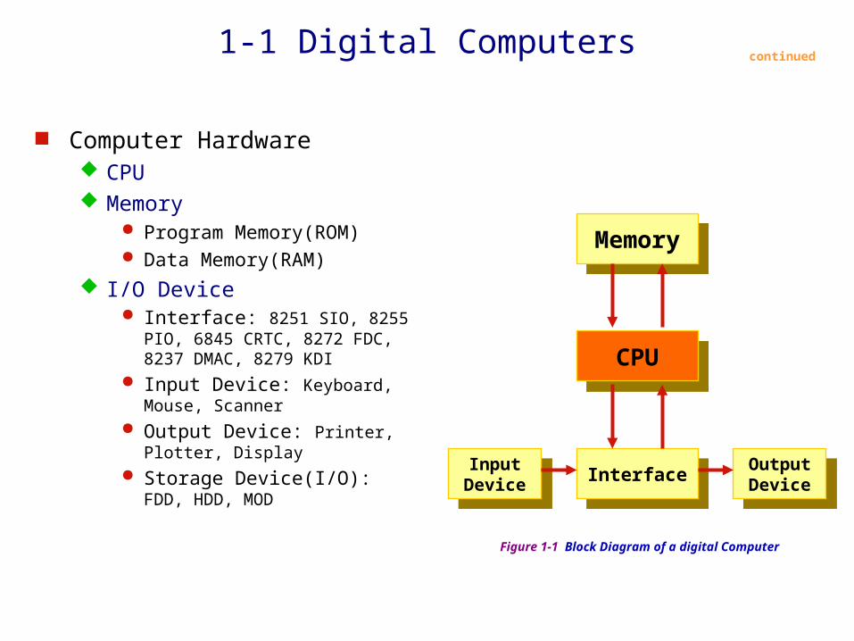
Computer Hardware CPU Memory
Program Memory(ROM) Data Memory(RAM)
I/O Device Interface: 8251 SIO, 8255 PIO,
6845 CRTC, 8272 FDC, 8237 DMAC, 8279 KDI
Input Device: Keyboard, Mouse, Scanner
Output Device: Printer, Plotter, Display
Storage Device(I/O): FDD, HDD, MOD
continued
MemoryMemory
CPUCPU
InterfaceInterfaceInputDevice
InputDevice
OutputDevice
OutputDevice
Figure 1-1 Block Diagram of a digital Computer

3 different point of view(Computer Hardware) Computer Organization(Chap 1 - 4)
H/W components operation/connection
Computer Design(Chap 5 - 7) H/W Design/Implementation
Computer Architecture(Chap 8, 9, 11, 12) Structure and behavior of the computer as seen by the user Information format, Instruction set, memory addressing, CPU, I/O, Memory
ISA(Instruction Set Architecture) the attributes of a system as seen by the programmer, i.e., the conceptual
structure and functional behavior, as distinct from the organization of the data flows and controls, the logic design, and the physical implementation.
- Amdahl, Blaaw, and Brooks(1964)
1-1 Digital Computerscontinued

1-1 Digital Computers
What is “Computer Architecture”?
- Hennessy and Patterson, Computer Organization and Design(1990) Computer Architecture
Instruction Set Architecture (ISA) Machine Organization
“ISA”? Instructions, Addressing modes, Instruction and data formats, Register
“Machine Organization”? CPU(Control, Data path), Memory, Input, Output
ADC(Analog to Digital Conversion) Signal Physical Quantity Binary Information
V, A, F, 거리 Discrete Value Gate
The manipulation of binary information is done by logic circuit called “gate”.
Fig. 1-2 Digital Logic Gates AND, OR, INVERTER, BUFFER, NAND, NOR, XOR, XNOR
1-2 Logic Gates
0 : 0.5
1 : 3
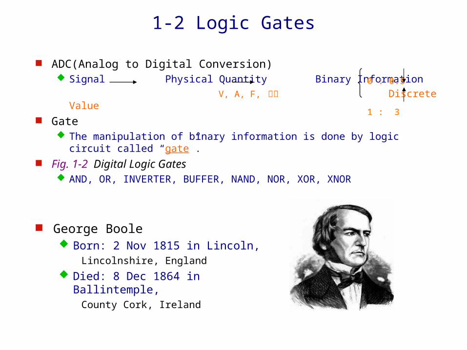
George Boole Born: 2 Nov 1815 in Lincoln,
Lincolnshire, England
Died: 8 Dec 1864 in Ballintemple, County Cork, Ireland
1-3 Boolean Algebra
Boolean Algebra Deals with binary variable(A, B, x, y: T/F or 1/0) + logic
operation(AND, OR, NOT…) Boolean Function: variable + operation
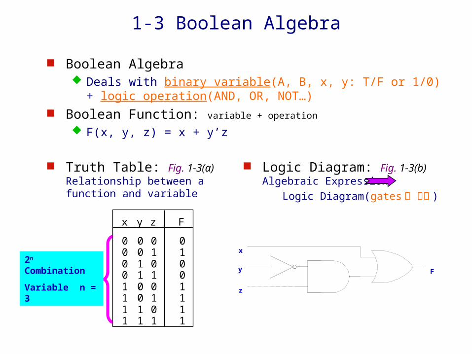
F(x, y, z) = x + y’z
Truth Table: Fig. 1-3(a) Relationship between a function and variable
x y z F
0 0 0 00 0 1 10 1 0 00 1 1 01 0 0 11 0 1 11 1 0 11 1 1 1
Logic Diagram: Fig. 1-3(b) Algebraic Expression
Logic Diagram(gates 로 표현 )
2n Combination
Variable n = 3
x
y
z
F
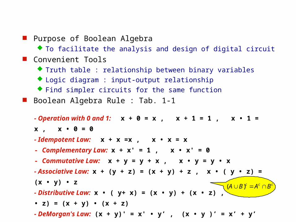
Purpose of Boolean Algebra To facilitate the analysis and design of digital circuit
Convenient Tools Truth table : relationship between binary variables Logic diagram : input-output relationship Find simpler circuits for the same function
Boolean Algebra Rule : Tab. 1-1
- Operation with 0 and 1: x + 0 = x , x + 1 = 1 , x • 1 = x , x • 0 = 0
- Idempotent Law: x + x =x , x • x = x
- Complementary Law: x + x' = 1 , x • x' = 0
- Commutative Law: x + y = y + x , x • y = y • x
- Associative Law: x + (y + z) = (x + y) + z , x • ( y • z) = (x • y) • z
- Distributive Law: x • ( y+ x) = (x • y) + (x • z) , x + (y • z) = (x + y) • (x + z)
- DeMorgan's Law: (x + y)' = x' • y’ , (x • y )’ = x’ + y’
General Form: (x1 + x2 + x3 + … xn)' = x1' • x2' • x3' • … xn’
(x1 • x2 • x3 • … xn) ' = x1' + x2' + x3' + … xn’
ccc BABA )(

Computer System Architecture Dept. of Info. Of Computer.Chap. 1 Digital Logic CircuitsChap. 1 Digital Logic Circuits
1-8Representation of Boolean Function
A Boolean function can be expressed algebraically in many ways Two ways of forming Boolean expression are Canonical Form and
Non Canonical Forms Canonical Forms express all binary variables in every product
(AND) or sum(OR) term of the Boolean Function. To determine the canonical sum of products form for a Boolean
Function F(A,B,C) = A’B + C’ + ABC which is in non-canonical form the following steps are used.

F= AB’ + C’D + AB’ + C’D
= x + x (let x= AB’ + C’D)
= x
= AB’ + C’D
F= ABC + ABC’ + A’C
= AB(C + C’) + A’C
= AB + A’C
1 inverter, 1 AND gate 감소
Fig. 1-6(a)
Fig. 1-6(b)
Fig. 1-4 2 graphic symbols for NOR gate
(a) OR-invert (b) invert-OR
Fig. 1-5 2 graphic symbols for NAND gate
(a) NAND-invert (b) invert-NAND
(x+y+z)’xyz
xyz
xyz
xyz
(x’+y’+z’)(xyz)’
x’ y’z’

1-4 Map Simplification
Karnaugh Map(K-Map) Map method for simplifying Boolean expressions
Minterm / Maxterm Minterm : n variables product ( x=1, x’=0) Maxterm : n variables sum (x=0, x’=1)
2 variables example
F = x’y + xy
x y Minterm Maxterm0 0 x'y' m0 x + y M0
0 1 x'y m1 x + y' M1
1 0 x y' m2 x'+ y M2
1 1 x y m3 x'+ y' M3
m0 + m1 + m2 + m3 M0 M1 M2 M3
m1 m3
)2,0(
)3,1(
(Complement = M0 M2 )
( m1 + m3 )

Map 2 variables 3 variables 4 variables
0 1
2 3A
B B
0 1 3 2
4 5 7 6A
C A
0 1 3 2
4 5 7 6
12 13 15 14
8 9 11 10
B
C
D
5 variables
0 1 3 2 6 7 5 4
8 9 11 10 14 15 13 12
24 25 27 26 30 31 29 28
16 17 19 18 22 23 21 20A
B
C
D FE

F= x + y’z
(1) Truth Table
x y z F Minterm
0 0 0 0 m0
0 0 1 1 m1
0 1 0 0 m2
0 1 1 0 m3
1 0 0 1 m4
1 0 1 1 m5
1 1 0 1 m6
1 1 1 1 m7
(2) )7,6,5,4,1(),,( zyxF(3)
z
x
y
0 1 3 2
4 5 7 6
F= x + y’z

Adjacent Square Number of square = 2n (2, 4, 8, ….) The squares at the extreme ends of the
same horizontal row are to be considered adjacent
The same applies to the top and bottom squares of a column
The four corner squares of a map must be considered to be adjacent
Groups of combined adjacent squares may share one or more squares with one or more group
0 1 3 2
4 5 7 6
0 1 3 2
4 5 7 6
12 13 15 14
8 9 11 10
0 1 3 2
4 5 7 6
0 1 3 2
4 5 7 6
12 13 15 14
8 9 11 10
0 1 3 2
4 5 7 6

F=AC’ + BC
)7,6,4,3(),,( CBAF
F=C’ + AB’
)6,5,4,2,0(),,( CBAF
B
0 1 3 2
4 5 7 6A
C B
0 1 3 2
4 5 7 6A
C
A
0 1 3 2
4 5 7 6
12 13 15 14
8 9 11 10
B
C
D
F=C’ + AB’
)10,9,8,6,2,1,0(),,,( DCBAF
A
0 1 3 2
4 5 7 6
12 13 15 14
8 9 11 10
B
C
D
Product-of-Sums Simplification
F=B’D’ + B’C’ + A’C’D
F’=AB + CD + BD’(square marked 0’s)
F’’(F)=(A’ + B’)(C’ + D’)(B’ + D)
)10,9,8,5,2,1,0(),,,( DCBAF
Sum of product
Product of Sum

NAND Implementation Sum of Product : F=B’D’ + B’C’ + A’C’D
NOR Implementation Product of Sum : F=(A’ + B’)(C’ + D’)(B’ + D)
Don’t care conditions F(A,B,C)=(0, 2, 6), d(A,B,C)= (1, 3, 5) F=A’ + BC’= (0, 1, 2, 3, 6)
B’D’
C’
A’D
A’B’C’D’
D’
A
B
0 1 3 2
4 5 7 6
C
X
X
X

1-5 Combinational Circuits
Combinational Circuits A connected arrangement of logic gates with a set of inputs and outputs Fig. 1-15 Block diagram of a combinational circuit
Analysis Logic circuits diagram Boolean function or Truth table
Design(Analysis)
1. The Problem is stated 2. I/O variables are assigned 3. Truth table(I/O relation) 4. Simplified Boolean Function(Map Boolean )
5. Logic circuit diagram
i0i1
in
f0f1
fm. .
.
. . .Combinational
Circuits(Logic Gates)
Experience

Design Example : Full Adder 1. Full adder is a combinational circuits that forms the arithmetic sume
of three input bit(Carry considered) 2. 3 Input(x, y, z), 2 Output(S: sum, C: carry) 3. Truth Table
Inputx y z C S0 0 0 0 00 0 1 0 10 1 0 0 10 1 1 1 01 0 0 0 11 0 1 1 01 1 0 1 01 1 1 1 1
Output
4. Simplificationy
0 1 3 2
4 5 7 6x
z
y
0 1 3 2
4 5 7 6x
z
C= xy’z + x’yz + xy
=z(xy’ + x’y) + xy
=z(x y) + xy
5. Logic circuit diagram
S=xy’z’ + x’y’z + xyz + x’yz’
= z’(xy’ + x’y) + z(x’y’ + xy)
= z’(x y) + z(x y)’
=a’b + ab’ (let a=z, b=x y)
=x y z
(x y)’=(xy’+x’y)’=(x’+y)(x+y’)=x’x+x’y’+xy+yy’=x’y’+xy
xy
z
c
s

JK(Jack/King) F/F
JK F/F is a refinement of the SR F/F The indeterminate condition of the SR
type is defined in complement
1-6 Flip-Flops
Flip-Flop The storage elements employed in clocked sequential circuit A binary cell capable of storing one bit of information
SR(Set/Reset) F/F
Combinational Circuit = Gate Sequential Circuit = Gate + F/F
Q
QSET
C LR
S
R
S R0 00 11 01 1 ? Indeterminate
Q(t+1) Q(t) no change 0 clear to 0 1 set to 1
D(Data) F/F
“no change” condition 이 없다 : Q(t+1)=D 1) Disable Clock
2) Feedback output into input
J
Q
Q
K
SET
C LR
D 01
Q(t+1) 0 clear to 0 1 set to 1
J K0 00 11 01 1 Q(t)' Complement
Q(t+1) Q(t) no change 0 clear to 0 1 set to 1
Q
QSET
C LR
D
T(Toggle) F/F
T=1(J=K=1), T=0(J=K=0) JK F/F Q(t+1)= Q(t) T
Q
QSET
C LR
T T01
Q(t+1) Q(t) no change Q'(t) Complement

Edge-Triggered F/F State Change : Clock Pulse
Rising Edge(positive-edge transition) Falling Edge(negative-edge transition)
Setup time(20ns) minimum time that D input must remain at constant value before the transition.
Hold time(5ns) minimum time that D input must not change after the positive transition.
Propagation delay(max 50ns) time between the clock input and the response in Q 일반 논리 gate 에서는 2-20 ns 이며 setup 및 hold time 은 F/F 에서만 정의되며 일반 논리
gate 에서는 정의되지 않음 . Master-Slave F/F
2 개의 F/F 을 사용 (Slave 와 Master F/F) 하며 negative-edge transition 사용 위와 같이 사용하는 이유 : Race 현상을 방지
ts th
Positive clock transition

Race 현상 조건 - Setup time > Propagation delay 증상 - 0 과 1 을 반복하다가 Unstable 한 상태가 된다 해결책 - Edge triggered F/F 또는 Master/Slave F/F 사용 예제
7470 : J-K Edge triggered F/F 7471 : J-K Master/Slave F/F
Excitation Table Required input combinations for a given change of state Present State 와 Next State 로 표현
Q(t) Q(t+1) S R 0 0 0 X 0 1 0 1 1 0 1 0 1 1 X 1
SR F/F Q(t) Q(t+1) D 0 0 0 0 1 1 1 0 0 1 1 1
D F/F Q(t) Q(t+1) J K 0 0 0 X 0 1 1 X 1 0 X 1 1 1 X 0
J K F/F Q(t) Q(t+1) T 0 0 0 0 1 1 1 0 1 1 1 0
T F/F
1 : Clear to 00 : No change
1 : Set to 10 : ComplementDon’t Care

1-7 Sequential Circuits
A sequential circuit is an interconnection of F/F and Gate Clocked synchronous sequential circuit
Flip-Flop Input Equation Boolean expression for F/F input Input Equation 예제
DA = Ax + Bx, DB = A’x
Output Equation y = Ax’ + Bx’
Fig. 1-25 Example of a sequential
circuit
Combinational Circuit = Gate Sequential Circuit = Gate + F/F
Combinational Circuit
Flip-Flops
Input Output
Clock
Q
QSET
C LR
D
Q
QSET
C LR
D
xDA
DB
A
A’
B
B’Clock
y

State Table Present state, input, next state, output 표현
Design Example: Binary Counter
Present State Input Next State Output
A B x Ax Bx DA DB A B y0 0 0 0 0 0 0 0 0 00 0 1 0 0 0 1 0 1 00 1 0 0 0 0 0 0 0 10 1 1 0 1 1 1 1 1 01 0 0 0 0 0 0 0 0 11 0 1 1 0 1 0 1 0 01 1 0 0 0 0 0 0 0 11 1 1 1 1 1 0 1 0 0
Input Equ.
Input Equ. = Next State
State Diagram Graphical representation of state
table Circle(state), Line(transition),
I/O(input/output)
00
01
10
11
0/0 1/0
1/00/1
1/0
0/1
0/1 1/0
Excitation Table(2 bit counter = 2 F/F)00
01
10
11
x=0 x=0
x=1
x=1
x=1 x=1
x=0 x=0
0/00
1/01
Present State InputA B x A B J A KA J B KB
0 0 0 0 0 0 x 0 x0 0 1 0 1 0 x 1 x0 1 0 0 1 0 x x 00 1 1 1 0 1 x x 11 0 0 1 0 x 0 0 x1 0 1 1 1 x 0 1 x1 1 0 1 1 x 0 x 01 1 1 0 0 x 1 x 1
Next State F/F Input Eq u .
x=1: 00, 01, 10, 11, 00, 01, ….. x=0: no change
State Diagram:
4 state(00, 01, 10, 11)
Next State =Output
Q(t) Q(t+1) J K 0 0 0 X 0 1 1 X 1 0 X 1 1 1 X 0
J K F/F

A
B
0 1 3 2
4 5 7 6
x
1
1
X X
X X
Map for simplification Input variable: A, B, x
A
B
0 1 3 2
4 5 7 6
x
A
B
0 1 3 2
4 5 7 6
x
A
B
0 1 3 2
4 5 7 6
x
JA
KB
KA
JB
JA=Bx
KA=xJB=x
KA=Bx
X X X X
X X X X
X X
X X
1
1
1
1 J
Q
Q
K
SET
CLR
J
Q
Q
K
SET
CLR
C loc k
x
B
A
Logic Diagram
Sequential Circuit Design Procedure 1-5 절 참고 (Combinational Circuit Design) Sequential Circuit 은 절차 3 에서 State
diagram 및 State table 이용 F/F 수 : 2m+n (m - State 수 , n - Input 수 )
1. The Problem is stated2. I/O variables are assigned3. Truth table(I/O relation)4. Simplified Boolean Function5. Logic circuit diagram
Top Related