Zynq Migration Guide: Zynq-7000 SoC to Zynq UltraScale+ ... · Integrating an Arm®-based...
156
Zynq Migration Guide Zynq-7000 SoC to Zynq UltraScale+ MPSoC Devices UG1213 (v3.0) November 22, 2019
Transcript of Zynq Migration Guide: Zynq-7000 SoC to Zynq UltraScale+ ... · Integrating an Arm®-based...

Zynq Migration Guide
Zynq-7000 SoC to Zynq UltraScale+ MPSoC Devices
UG1213 (v3.0) November 22, 2019
Zynq Migration Guide 2UG1213 (v3.0) November 22, 2019 www.xilinx.com
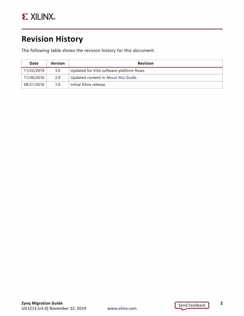
Revision HistoryThe following table shows the revision history for this document.
Date Version Revision11/22/2019 3.0 Updated for Vitis software platform flows.11/30/2016 2.0 Updated content in About this Guide.09/21/2016 1.0 Initial Xilinx release.
Send Feedback

Table of ContentsRevision History . . . . . . . . . . . . . . . . . . . . . . . . . . . . . . . . . . . . . . . . . . . . . . . . . . . . . . . . . . . . . . . . . . . . 2
Chapter 1: IntroductionAbout this Guide . . . . . . . . . . . . . . . . . . . . . . . . . . . . . . . . . . . . . . . . . . . . . . . . . . . . . . . . . . . . . . . . . . 5Pre-Requisites . . . . . . . . . . . . . . . . . . . . . . . . . . . . . . . . . . . . . . . . . . . . . . . . . . . . . . . . . . . . . . . . . . . . 6Document Audience and Scope . . . . . . . . . . . . . . . . . . . . . . . . . . . . . . . . . . . . . . . . . . . . . . . . . . . . . . 6Zynq Device Comparison . . . . . . . . . . . . . . . . . . . . . . . . . . . . . . . . . . . . . . . . . . . . . . . . . . . . . . . . . . . . 7Hardware Differences in Zynq Devices. . . . . . . . . . . . . . . . . . . . . . . . . . . . . . . . . . . . . . . . . . . . . . . . . 7Development Tools . . . . . . . . . . . . . . . . . . . . . . . . . . . . . . . . . . . . . . . . . . . . . . . . . . . . . . . . . . . . . . . 18Migration Flow. . . . . . . . . . . . . . . . . . . . . . . . . . . . . . . . . . . . . . . . . . . . . . . . . . . . . . . . . . . . . . . . . . . 19
Chapter 2: Processing UnitsProgrammer Models for Zynq Architectures . . . . . . . . . . . . . . . . . . . . . . . . . . . . . . . . . . . . . . . . . . . 23Clocking. . . . . . . . . . . . . . . . . . . . . . . . . . . . . . . . . . . . . . . . . . . . . . . . . . . . . . . . . . . . . . . . . . . . . . . . . 28Registers . . . . . . . . . . . . . . . . . . . . . . . . . . . . . . . . . . . . . . . . . . . . . . . . . . . . . . . . . . . . . . . . . . . . . . . . 34Programming Flow. . . . . . . . . . . . . . . . . . . . . . . . . . . . . . . . . . . . . . . . . . . . . . . . . . . . . . . . . . . . . . . . 37Reset System . . . . . . . . . . . . . . . . . . . . . . . . . . . . . . . . . . . . . . . . . . . . . . . . . . . . . . . . . . . . . . . . . . . . 39System Test and Debug . . . . . . . . . . . . . . . . . . . . . . . . . . . . . . . . . . . . . . . . . . . . . . . . . . . . . . . . . . . . 41
Chapter 3: Migrating SoftwareIntroduction . . . . . . . . . . . . . . . . . . . . . . . . . . . . . . . . . . . . . . . . . . . . . . . . . . . . . . . . . . . . . . . . . . . . . 43Migrating Software from Zynq-7000 SoC APU to Zynq UltraScale+ MPSoC APU/RPU . . . . . . . . . . 43
Chapter 4: PeripheralsIntroduction . . . . . . . . . . . . . . . . . . . . . . . . . . . . . . . . . . . . . . . . . . . . . . . . . . . . . . . . . . . . . . . . . . . . . 47I2C Controller . . . . . . . . . . . . . . . . . . . . . . . . . . . . . . . . . . . . . . . . . . . . . . . . . . . . . . . . . . . . . . . . . . . . 47UART Controller . . . . . . . . . . . . . . . . . . . . . . . . . . . . . . . . . . . . . . . . . . . . . . . . . . . . . . . . . . . . . . . . . . 51CAN Controller . . . . . . . . . . . . . . . . . . . . . . . . . . . . . . . . . . . . . . . . . . . . . . . . . . . . . . . . . . . . . . . . . . . 56SPI Controller . . . . . . . . . . . . . . . . . . . . . . . . . . . . . . . . . . . . . . . . . . . . . . . . . . . . . . . . . . . . . . . . . . . . 62Gigabit Ethernet Controller . . . . . . . . . . . . . . . . . . . . . . . . . . . . . . . . . . . . . . . . . . . . . . . . . . . . . . . . . 67USB Controller . . . . . . . . . . . . . . . . . . . . . . . . . . . . . . . . . . . . . . . . . . . . . . . . . . . . . . . . . . . . . . . . . . . 76General Purpose I/O . . . . . . . . . . . . . . . . . . . . . . . . . . . . . . . . . . . . . . . . . . . . . . . . . . . . . . . . . . . . . . 84Multiplexed I/O . . . . . . . . . . . . . . . . . . . . . . . . . . . . . . . . . . . . . . . . . . . . . . . . . . . . . . . . . . . . . . . . . . 93
Zynq Migration Guide 3UG1213 (v3.0) November 22, 2019 www.xilinx.com
Send Feedback

DMA Controller . . . . . . . . . . . . . . . . . . . . . . . . . . . . . . . . . . . . . . . . . . . . . . . . . . . . . . . . . . . . . . . . . 137
Chapter 5: Boot and ConfigurationBooting Option Differences. . . . . . . . . . . . . . . . . . . . . . . . . . . . . . . . . . . . . . . . . . . . . . . . . . . . . . . . 144Boot Image Header Format . . . . . . . . . . . . . . . . . . . . . . . . . . . . . . . . . . . . . . . . . . . . . . . . . . . . . . . . 147
Chapter 6: LibrariesIntroduction . . . . . . . . . . . . . . . . . . . . . . . . . . . . . . . . . . . . . . . . . . . . . . . . . . . . . . . . . . . . . . . . . . . . 148Standalone BSP . . . . . . . . . . . . . . . . . . . . . . . . . . . . . . . . . . . . . . . . . . . . . . . . . . . . . . . . . . . . . . . . . 148
Appendix A: Additional Resources and Legal NoticesXilinx Resources . . . . . . . . . . . . . . . . . . . . . . . . . . . . . . . . . . . . . . . . . . . . . . . . . . . . . . . . . . . . . . . . . 153Solution Centers. . . . . . . . . . . . . . . . . . . . . . . . . . . . . . . . . . . . . . . . . . . . . . . . . . . . . . . . . . . . . . . . . 153Documentation Navigator and Design Hubs . . . . . . . . . . . . . . . . . . . . . . . . . . . . . . . . . . . . . . . . . . 153References . . . . . . . . . . . . . . . . . . . . . . . . . . . . . . . . . . . . . . . . . . . . . . . . . . . . . . . . . . . . . . . . . . . . . 154Training Resources. . . . . . . . . . . . . . . . . . . . . . . . . . . . . . . . . . . . . . . . . . . . . . . . . . . . . . . . . . . . . . . 155Third-Party Documentation . . . . . . . . . . . . . . . . . . . . . . . . . . . . . . . . . . . . . . . . . . . . . . . . . . . . . . . 155Please Read: Important Legal Notices . . . . . . . . . . . . . . . . . . . . . . . . . . . . . . . . . . . . . . . . . . . . . . . 156
Zynq Migration Guide 4UG1213 (v3.0) November 22, 2019 www.xilinx.com
Send Feedback

Chapter 1
Introduction
About this GuideThe Zynq® UltraScale+™ MPSoC device is the successor to the Zynq®-7000 SoC device. It provides 64-bit processor scalability while combining real-time control with soft and hard engines for graphics, video, waveform, and packet processing, to name a few.
Integrating an Arm®-based heterogeneous system for advanced analytics and on-chip programmable logic for compute task acceleration creates unlimited possibilities for applications.
This document facilitates the migration of designs from a Zynq-7000 SoC device to a Zynq UltraScale+ MPSoC device.
The Zynq UltraScale+ MPSoC family has different products, based upon the following system features:
• Application processing unit (APU):
° Dual or Quad-core Arm Cortex-A53 MPCore™
° CPU frequency up to 1.5 GHz• Real-time processing unit (RPU):
° Dual-core Arm Cortex-R5F MPCore
° CPU frequency up to 600 MHz• Graphics processing unit (GPU):
° Arm Mali™-400 MP2
° GPU frequency up to 667 MHz
Zynq Migration Guide 5UG1213 (v3.0) November 22, 2019 www.xilinx.com
Send Feedback

Chapter 1: Introduction
• Video codec unit (VCU):
° Simultaneous Encode and Decode through separate cores
° H.264 high profile level 5.2 (4Kx2K-60)
° H.265 (HEVC) main, main10 profile, level 5.1, high Tier, up to 4Kx2K-60 rate
° 8-bit and 10-bit encoding
° 4:2:0 and 4:2:2 chroma sampling
For more details, see the Zynq UltraScale+ MPSoC Product Page [Ref 3] and the Product Advantages [Ref 4].
Pre-RequisitesThis document assumes that you have the following qualifications:
• Familiarity with the Zynq-7000 SoC device• Experienced with application development for a Zynq-7000 SoC device• Experienced with embedded software development
Document Audience and ScopeThe purpose of this guide is to enable software developers and system architects to be familiar with:
• Hardware features and differences between a Zynq-7000 SoC device and a Zynq UltraScale+ MPSoC device
• Porting the software application from Zynq-7000 SoC device to a Zynq UltraScale+ MPSoC device
• Interfacing peripheral configuration differences between Zynq-7000 SoC device and a Zynq UltraScale+ MPSoC device
• Booting differences between the Zynq-7000 SoC device and a Zynq UltraScale+ MPSoC device
Zynq Migration Guide 6UG1213 (v3.0) November 22, 2019 www.xilinx.com
Send Feedback

Chapter 1: Introduction
Zynq Device ComparisonThe Zynq-7000 SoC device, built on 28 nm processing technology from TSMC, combines an industry-standard Arm® dual-core Cortex™-A9 MPCore™ processing system with Xilinx 28 nm programmable logic. This processor-centric architecture delivers a comprehensive processing platform that offers developers ASIC levels of performance and power consumption, the ease of programmability of a microprocessor and the flexibility of a FPGA.
The Zynq UltraScale+ MPSoC device is built on 16FinFET+ processing technology from TSMC in the Arm-based multiprocessor cores. Building on the industry success of the Zynq-7000 SoC device family, the new Zynq UltraScale+ MPSoC device architecture extends Xilinx® SoC devices to enable true heterogeneous multi-processing with the right engines for the right tasks for smarter systems.
This chapter gives the overview of the procedure involved in the migration process by highlighting the hardware differences between the Zynq-7000 SoC device and the Zynq UltraScale+ MPSoC device.
Hardware Differences in Zynq DevicesThe Zynq family offers the flexibility and scalability of an FPGA, while providing performance, power, and ease of use typically associated with ASIC and ASSP chips. Both the Zynq devices combine the Arm®- based processing system (PS) with Xilinx programmable logic (PL).
• In the Zynq UltraScale+ MPSoC device, the Xilinx memory protection unit (XMPU) provides memory partitioning and TrustZone (TZ) protection for memory and FPD slaves. The XMPU can be configured to isolate a master or a given set of masters to a programmable set of address ranges.
• In the Zynq UltraScale+ MPSoC device, the Xilinx peripheral protection unit (XPPU) provides LPD peripheral isolation and inter-processor interrupt (IPI) protection. The XPPU can be configured to permit one or more masters to access an LPD peripheral without knowing the address aperture of the peripheral.
Zynq Migration Guide 7UG1213 (v3.0) November 22, 2019 www.xilinx.com
Send Feedback

Chapter 1: Introduction
For more information about XPMU and XPPU, and role of IPIs, see this link to the “PMU Interconnect” sub-section in the “Platform Management Unit” chapter of the Zynq UltraScale+ MPSoC Technical Reference Manual (UG1085).
The following figure shows the top-level block diagram of PS in the Zynq devices.
The PS of the Zynq-7000 SoC device comprises:
• An application processing unit (APU)• Memory interfaces• System control• Central interconnect• I/O peripherals
The PS of Zynq UltraScale+ MPSoC device combines a heterogeneous processing system comprising the following:
• Application processing unit (APU)• Real-time processing unit (RPU)
X-Ref Target - Figure 1-1
Figure 1-1: Top-Level PS Diagram for the Zynq Devices
Zynq Migration Guide 8UG1213 (v3.0) November 22, 2019 www.xilinx.com
Send Feedback

Chapter 1: Introduction
• Graphics processing unit (GPU) with memory interfaces• System control• Central interconnect• I/O peripherals
Processing System DifferencesThe Zynq UltraScale+ MPSoC devices also provides the following units to enhance the run-time security of a software.
• Xilinx Memory Protection Unit (XMPU)• Xilinx Peripheral Protection Unit (XPPU)• System Memory Management Unit (SMMU)
The following table summarizes the PS architectural differences between the Zynq devices..
Table 1-1: Processor System Block ComparisonPS Block Name Zynq-7000 SoC Zynq UltraScale+ MPSoC
Application Processing Unit • Dual core Arm Cortex-A9 32-bit processor,
• Includes accelerator coherency port.
• Dual and Quad core Cortex-A53 64-bit processors. Supports four exception layers.
• Includes accelerator coherency port and AXI coherency extension.
Real-time Processing Unit • Arm Instruction set (Armv7a) • Arm v7-R instruction set.• Dynamic branch prediction.• Redundant CPU logic for fault
detection. • AXI interface to PL for low
latency applications.Graphic Processing Unit
-
• One geometry processor.• Two pixel processors• OpenGL ES 1.1 and 2.0
support.• OpenVG 1.1• Advanced anti-aliasing
support.Interconnect • Arm AMBA 3.0 interconnect
• Switches based on Arm NIC-301
• Arm AMBA 4.0 interconnect.• Switches based on Arm
NIC-400.Max I/O Pins • 128 • 214
Zynq Migration Guide 9UG1213 (v3.0) November 22, 2019 www.xilinx.com
Send Feedback

Chapter 1: Introduction
Configuration Security Unit
-
• Triple redundant processor for controlling boot flow.
• Supports secure and non-secure boot.
• Includes a crypto engine that contains AES-GCM
• supports SHA-3 and RSA standards.
Power Domains Has power domains:• PS power domain• PL power domain
Has power domains:• Full-Power Domain (FPD)• Low-Power Domain (LPD)• Battery Power Domain• PL Power Domain
Platform Management Unit (PMU)
-
• Triple redundant processors.• Does system initialization
during boot. • Power gating and retention
states management.• Sleep state management.
Interrupts • APU handles the interrupts using GIC pl390.
• GIC dispatches the interrupts to the individual CPU
• APU handles the interrupts using GIC400.
• RPU uses GIC390. • GIC takes all the interrupts
and generates interrupts for the PMU.
Timers • Has a 24-bit WDT• Two 16-bit TTC• Each Cortex-A9 processor has
its own private 32-bit timer and 32-bit WDT
• Both processors share a global 64-bit timer.
• Has two SWDT; one each for RPU and APU.
• Two 32-bit TTC for each RPU and APU.
• System has a Generic 64-bit counter.
Table 1-1: Processor System Block Comparison (Cont’d)
PS Block Name Zynq-7000 SoC Zynq UltraScale+ MPSoC
Zynq Migration Guide 10UG1213 (v3.0) November 22, 2019 www.xilinx.com
Send Feedback

Chapter 1: Introduction
DMA Controller • Supports simple and scatter-gather mode.
• provides eight concurrent DMA channel threads
• Supports multi-channel data FIFO
• Has two instances of DMA controller:° FPD-DMA° LPD-DMA
• Programmable number of outstanding transfers.
• Support for simple and scatter-gather mode.
• Support for read-only and write-only DMA mode.
• Descriptor pre-fetching, per channel flow control interface.
DDR Memory Controller • Supports DDR2, DDR3, DDR3L, and LPDDR2.
• Configurable 16-bit or 32-bit data bus.
• ECC support for 16-bit mode.
• Support for DDR3, DDR3L, DDR4, LPDDR4, up to two ranks.
• Dynamic scheduling to optimize bandwidth and latency.
• ECC support in 32-bit and 64-bit mode
• Software programmable quality of service.
NAND Memory Controller • Complies with ONFI 1.0.• Supports asynchronous
memory operating mode.
• Complies with ONFI 3.1 specification.
• Supports reset logical unit number.
• ODT configuration, on-die termination.
SPI Controller • Full duplex operation.• Supports multi-master I/O
mode.• Selectable master clock
reference.
• Full duplex operation.• Multi-master environment
support• Programmable master mode
clock frequency.• programmable transmission
format.
Table 1-1: Processor System Block Comparison (Cont’d)
PS Block Name Zynq-7000 SoC Zynq UltraScale+ MPSoC
Zynq Migration Guide 11UG1213 (v3.0) November 22, 2019 www.xilinx.com
Send Feedback

Chapter 1: Introduction
Quad-SPI Controller • Consists of a Legacy linear Quad-SPI controller.
• Consists of a Legacy linear Quad-SPI controller and a new generic Quad-SPI controller.
• Supports command queuing.• Supports 4/8 bit interface.• 44-bit address support on AXI
in DMA mode transfer.
CAN Controller • Complies with ISO 11898 -1.• CAN 2.0A, and CAN 2.0B
standards.• Supports both standard
(11-bit identifier) and extended (29-bit identifier) frames
• Complies with ISO 11898 -1.• CAN 2.0A, and CAN 2.0B
standards. • Supports both standard
(11-bit identifier) and extended (29-bit identifier) frames.
UART Controller • Programmable baud rate generator.
• 6/7/8 data bits modem control signals.
• Programmable baud rate generator.
• 6/7/8 data bits modem control signals.
I2C Controller • I2C bus specification version 2.0 supported.
• I2C bus specification version 2.0 supported.
SD/SDIO Controller • Compatible with the standard SD Host Controller Specification, version 2.0 Part A2.
• Compatible with the SD host controller standard specification version 3.00.
General-purpose I/O • Up to 54 GPIO signals for device pins routed through the MIO.
• 192 GPIO signals between the PS and PL using the EMIO.
• 78 GPIO signals for device pins.
• 288 GPIO signals between PS-PL interface through EMIO.
USB Controller • Has two USB 2.0 controllers • Has two USB 3.0 controllers and is backward compatible with USB 2.0.
• Provides simultaneous operation of the USB 2.0 and USB 3.0 interfaces only in Host mode.
Table 1-1: Processor System Block Comparison (Cont’d)
PS Block Name Zynq-7000 SoC Zynq UltraScale+ MPSoC
Zynq Migration Guide 12UG1213 (v3.0) November 22, 2019 www.xilinx.com
Send Feedback

Chapter 1: Introduction
PS PCI Express
-
• PCI Express (Specification 2.1) as part of PS.
• Interlaken• 100G Ethernet Block• System Monitor
Gigabit transceiver interface • Compliant with PCIe 2.1• Low power gigabit transceiver
is capable of up to 12.5 Gb/s line rates with flip-chip packages and up to 6.6Gb/s with bare-die flip-chip packages.
• Compliant with PCIe 2.1• USB 3.0• DisplayPort 1.2a• SGMII• SATA 3.1 PHY protocols.
Gigabit Ethernet controller • Compatible with the IEEE 802.3-2008 standard capable of operating in either half or full duplex mode at all three (10/100/1000 Mb/s) speeds.
• To access pins using MIO, each controller uses an RGMII interface, and access to the PL through the EMIO provides the GMII interface.
• IEEE Std 802.3-2008 compatible
• Full and half-duplex modes of operation
• RGMII/SGMII interface support
• Jumbo frame support• Automatic discard frames
with errors• Programmable inter-packet
gap• Full-duplex flow control. • The controller has a built-in
DMA engine for transferring Ethernet packets from memory.
SATA host controller Interface
-
• Compliant with the SATA 3.1 specification.
• Supports 1.5G, 3G, and 6G line rates.
• Compliant with the advanced host controller interface version 1.3.
• The controller has an embedded DMA that facilitates memory transfers.
DisplayPort interface
-
• Source only controller with an embedded DMA block that supports 1G or 2G transceiver lanes.
• Supports real time video and audio input from the PL.
Table 1-1: Processor System Block Comparison (Cont’d)
PS Block Name Zynq-7000 SoC Zynq UltraScale+ MPSoC
Zynq Migration Guide 13UG1213 (v3.0) November 22, 2019 www.xilinx.com
Send Feedback

Chapter 1: Introduction
Programmable Logic DifferencesIn both Zynq-7000 SoC and Zynq UltraScale+ MPSoC devices, the PL can be on a separate power domain from PS, enabling your design to save power by completely shutting down the PL when the PL is not in use. The following table lists the PL differences between the Zynq devices.
For more information regarding resource counts, see the Xilinx Silicon Devices [Ref 2] website.
Table 1-2: Programmable Logic ComparisonProgrammable Logic Features Zynq-7000 SoC Zynq UltraScale+ MPSoC
FPGA • Uses Xilinx 7 series (Artix®-7/Kintex®-7) 28 nm technology.
• Uses UltraScale+ 16 nm technology (Kintex/Virtex® UltraScale+™).
Block RAM • Dual Port 36 Kb blocks configurable as dual 18 Kb, up to 72 bits wide.
• Max memory is 26.5 Mb.
• True dual port 36 Kb blocks configurable as dual 18 Kb, up to 72 bits wide
• Max memory is 70.6 Mb.Maximum I/O Pins 250 668UltraRAM
-• 288 Kb dual port.• 72-bit wide error checking and
correction.Maximum Logic Cells 444K 1143KDSP Slices • 25 × 18 two's complement
multiplier• A 48-bit accumulator • Optional pipelining,• Optional ALU• Dedicated buses for cascading
• 27 × 18 bit two’s complement multiplier
• A 48-bit accumulator• Optional pipelining• Optional ALU• Dedicated buses for cascading
Maximum Memory (Mb) 26.5 70.6PL PCI Express PCI Express (specification 2.1) as
a block in PL• PCI Express (specification 2.1)
as part of the PS• PCIe 4.0• Interlaken• 100G Ethernet block• System monitor block• Video Coder/Encoded block
PL Gigabit transceiver Compliant with PCIe 2.1 • Compliant with:° PCIe 2.1° USB 3.0° DisplayPort 1.2a° SGMII and SATA protocols
Zynq Migration Guide 14UG1213 (v3.0) November 22, 2019 www.xilinx.com
Send Feedback

Chapter 1: Introduction
System Address MapThis section provides a quick reference for comparing the system level address map of Zynq-7000 SoC device and the Zynq UltraScale+ MPSoC device.
• The Zynq-7000 SoC device uses 32-bit Arm Cortex-A9 processors.• The Zynq UltraScale+ MPSoC device uses 64-bit Arm Cortex-A53 processors, allowing
the software to access a much larger address map compared to Zynq-7000 SoC device.
IMPORTANT: Though the Zynq UltraScale+ MPSoC device supports 64-bit addressing, the lower 4GB address map provides apertures for all the peripherals to be able to work in 32-bit mode.
The following table shows the comprehensive comparison of system level address map of the Zynq-7000 SoC and Zynq UltraScale+ MPSoC devices.
Table 1-3: System-Level Address MapAddress Range Zynq-7000 SoC Zynq UltraScale+ MPSoC
0000_0000 to 0000_FFFF OCM DDR
0001_0000 to 0002_FFFD DDR DDR0002_FFFE to 0003_FFFF Reserved DDR0004_0000 to 0005_FFFF DDR DDR0006_0000 to 0007_FFFF Reserved DDR0008_0000 to 000B_FFFF DDR DDR
000C_0000 to 000F_FFFF Reserved DDR0010_0000 to 3FFF_FFFF DDR DDR4000_0000 to 7FFF_FFFF PL DDR8000_0000 to 9FFF_FFFF PL LPD-PL InterfaceA000_0000 to AFFF_FFFF PL FPD-PL (HPM0) InterfaceB000_0000 to BFFF_FFFF PL FPD-PL (HPM1) InterfaceC000_0000 to DFFF_FFFF Reserved Quad-SPIE000_0000 to E02F_FFFF IOP Lower PCIeE030_0000 to E0FF_FFFF Reserved Lower PCIeE100_0000 to E5FF_FFFF SMC Lower PCIeE600_0000 to EFFF_FFFF Reserved Lower PCIeF000_0000 to F7FF_FFFF Reserved ReservedF800_0000 to F800_0BFF SLCR Peripheral Register MapF800_1000 to F880_FFFF PS Peripheral Register Map
Zynq Migration Guide 15UG1213 (v3.0) November 22, 2019 www.xilinx.com
Send Feedback

Chapter 1: Introduction
PS I/O Peripheral RegistersThe following table shows the comparison of Zynq-7000 SoC and Zynq UltraScale+ MPSoC devices register base addresses of all the I/O peripherals that are placed within the first 4GB space of the Zynq UltraScale+ MPSoC device.
F890_0000 to F8F0_2FFF CPU Peripheral Register MapF8F0_3000 to FBFF_FFFF Reserved Peripheral Register MapFC00_0000 to FDFF_FFFF Quad-SPI Peripheral Register MapFE00_0000 to FFCF_FFFF Reserved Peripheral Register MapFFD0_0000 to FFFB_FFFF Reserved Peripheral Register MapFFFC_0000 to FFCF_FFFF OCM OCMFFD0_0000 to FFFD_FFFF OCM CSU/PMU/TCM/OCMFFFE_0000 to FFFF_FFFF Reserved CSU/PMU/TCM/OCM1_0000_0000 to 3_FFFF_FFFF - Reserved4_0000_0000 to 4_FFFF_FFFF - PL5_0000_0000 to 6_FFFF_FFFF - PCIe7_0000_0000 to F_FFFF_FFFF - DDR10_0000_0000 to 7F_FFFF_FFFF - PL80_0000_0000 to BF_FFFF_FFFF - PCIeC0_0000_0000 to FF_FFFF_FFFF - Reserved100_0000_0000 to FFF_FFFF_FFFF - PL
Table 1-4: PS I/O Peripheral comparison
Peripherals Base Address in Zynq-7000 SoC Base Address in Zynq UltraScale+ MPSoC
UART Controllers 0, 1 0xE000_0000, 0xE000_1000 0xFF00_0000, 0xFF01_0000
USB Controllers 0, 1 0xE000_2000, 0xE000_3000 0xFF9D_0000, 0xFF9E_0000I2C Controllers 0, 1 0xE000_4000, 0xE000_5000 0xFF02_0000, 0xFF03_0000SPI Controllers 0, 1 0xE000_6000, 0xE000_7000 0xFF04_0000, 0xFF05_0000CAN Controllers 0, 1 0xE000_8000, 0xE000_9000 0xFF06_0000, 0xFF07_0000GPIO Controller 0xE000_A000 0xFF0A_0000Ethernet Controllers 0, 1, 2, 3 0xE000_B000, 0xE000_C00, NA, NA 0xFF0B_0000, 0xFF0C_0000,
0xFF0D_0000, 0xFF0E_0000Quad-SPI Controller 0xE000_D000 0xFF0F_0000
Table 1-3: System-Level Address Map (Cont’d)
Address Range Zynq-7000 SoC Zynq UltraScale+ MPSoC
Zynq Migration Guide 16UG1213 (v3.0) November 22, 2019 www.xilinx.com
Send Feedback

Chapter 1: Introduction
SLCR RegistersThe following table compares the SLCR register base addresses of the Zynq-7000 SoC device and the Zynq UltraScale+ MPSoC device.
Static Memory Controller (SMC)
0xE000_E000 0xFF10_0000
SDIO Controllers 0, 1 0xE010_0000, 0xE010_1000 0xFF16_0000, 0xFF17_0000
Table 1-5: SLCR Register Comparison
Description Zynq-7000 SoC Base Address Zynq UltraScale+ MPSoC Base Address
SLCR write protection lock and security 0xF800_0000 0xFD610000 (FPD)
0xFF410000 (LPD)Clock control and status 0xF800_0100 0xFD1A0000 (FPD)
0xFF5E0000 (LPD)Reset control and status 0xF800_0200 0xFD1A0000 (FPD)
0xFF5E0000 (LPD)APU control 0xF800_0300 0xFD5C_0000TrustZone control
0xF800_0400
0xFD69_0000 (FPD Trustzone Control)0xFF4B_0000 (FPD Trustzone Control)
CoreSight SoC debug control
0xF800_0500
0xFEC10000 (CORESIGHT_A53_DBG_0)0xFED10000 (CORESIGHT_A53_DBG_1)0xFEE10000 (CORESIGHT_A53_DBG_2)0xFEF10000 (CORESIGHT_A53_DBG_3)0xFEBF0000 (CORESIGHT_R5_DBG_0)0xFEBF2000 (CORESIGHT_R5_DBG_1)
DDR DRAM controller 0xF800_0600 0xFD070000 MIO pin configuration 0xF800_0700 0xFF18_0000On-chip memory (OCM) control 0xF800_0A00 0xFF960000
Table 1-4: PS I/O Peripheral comparison (Cont’d)
Peripherals Base Address in Zynq-7000 SoC Base Address in Zynq UltraScale+ MPSoC
Zynq Migration Guide 17UG1213 (v3.0) November 22, 2019 www.xilinx.com
Send Feedback

Chapter 1: Introduction
Miscellaneous PS RegistersThe following table lists the corresponding addresses in the Zynq device PS registers.
Development ToolsTo maximize system performance and enable accelerated and predictable design cycles, Xilinx provides a comprehensive set of tools for hardware and software development for the Zynq-7000 SoC and Zynq UltraScale+ MPSoC devices.
Software Development Tools• Vitis Software Development Platform: This tool supports Zynq-7000 SoC devices and
also supports Zynq UltraScale+ MPSoC devices with additional features. The Vitis software development platform provides an environment for creating software platforms and applications targeted for Xilinx embedded processors. It works with hardware designs created with Vivado tools and is based on the Eclipse open source standard.
• PetaLinux Tools: This tool supports Zynq-7000 SoC devices and also supports Zynq UltraScale+ MPSoC devices with additional features. The PetaLinux tools offers everything necessary to customize, build, and deploy embedded Linux solutions on Xilinx processing systems. Tailored to accelerate design productivity for Zynq UltraScale+ MPSoC-like devices, the solution works with the Xilinx hardware design tools to facilitate the development of Linux systems for the Zynq UltraScale+ MPSoC device. See the PetaLinux Product Page [Ref 1] for more information about PetaLinux.
Table 1-6: PS Register Comparison
Description Zynq-7000 SoC Base Address Zynq UltraScale+ MPSoC Base Address
Triple Timer Counter (TTC 0, TTC 1, TTC 2, TTC 3)
0xF800_1000, 0xF800_2000, NA, NA
0xFF11_0000, 0xFF12_0000, 0xFF13_0000, 0xFF14_0000
System Watchdog Timer (SWDT) 0xF800_5000 0xFF15_0000AXI_HP 0 high performance AXI interface
0xF800_8000 0xFD38_0000
AXI_HP 1 high performance AXI interface
0xF800_9000 0xFD39_0000
AXI_HP 2 high performance AXI interface
0xF800_A000 0xFD3A_0000
AXI_HP 3 high performance AXI interface
0xF800_B000 0xFD3B_0000
Zynq Migration Guide 18UG1213 (v3.0) November 22, 2019 www.xilinx.com
Send Feedback
Chapter 1: Introduction
• Embedded Energy Management Framework: The embedded energy management interface (EEMI) and the power management framework (PMF) provides APIs that are targeted for Xilinx Zynq UltraScale+ MPSoC devices. This framework enables software running on different processing units (PUs) on the same device to communicate power control messages through a power management controller.
This controller responds to power management requests such as putting devices in to sleep mode, or removing power from an element completely.
Processor Units, such as the APU, RPU, and GPU use the API for Xilpm, a Xilinx library, while the power management unit (PMU) runs the PMU firmware application (PMUFW) that contains the necessary API to successfully interact with the power control signals from the processor units (PUs) and to receive and direct various power commands on hardware elements into different power states.
• QEMU: The quick emulator (QEMU) for Zynq UltraScale+ MPSoC devices provides a system-emulation-model that runs on an Intel-compatible Linux host system. See the Zynq UltraScale+ MPSoC QEMU User Guide (UG1169) [Ref 12] for more information about QEMU.
• Third-Party Tools: Many third-party tools, such as like Arm DS-5 Development Studio and Lauterbach tools, support the software development for Zynq UltraScale+ MPSoC devices.
Hardware Development Tools• Vivado Design Suite: The Vivado Design Suite offers a new approach for ultra-high
productivity with next generation C/C++ and IP-based design with the new HLx editions including HL System Edition, HL Design Edition, and HL WebPACK Edition.
Migration FlowThis section explains the steps for migrating an application from a Zynq-7000 SoC device to a Zynq UltraScale+ MPSoC device with a flow diagram. The following figure shows the flow diagram illustrating the steps of the migration.
Zynq Migration Guide 19UG1213 (v3.0) November 22, 2019 www.xilinx.com
Send Feedback

Chapter 1: Introduction
1. Install the required development tools: Because the Zynq UltraScale+ MPSoC device addresses a wide range of applications, Xilinx provides many development tools to reduce the application development cycle and thus reducing the product
X-Ref Target - Figure 1-2
Figure 1-2: Migration Flow
Start
1. Install the required development tools
2. Configure the required processors
3. Configure PS/PL Peripherals
4. Migrate the PL Design
5. Migrate the software application to the desired
processor
6. Generate the Boot Files
7. Validate on Hardware
Zynq Migration Guide 20UG1213 (v3.0) November 22, 2019 www.xilinx.com
Send Feedback

Chapter 1: Introduction
time-to-market. It is important to choose a right tool for the application development to avail the benefits of the Xilinx development tools. See Development Tools to know the different available Xilinx development tools.
2. Configure the required processors: The Zynq UltraScale+ MPSoC device has multiple processing units like the application processing unit (APU), the real-time processing unit (RPU), and the graphics processing unit (GPU). You can choose to migrate your application to APU or RPU depending on your application requirement, and accordingly configure the required processing unit. To understand more about configuring APU/RPU, see Chapter 2, Processing Units.
3. Configure the PS/PL Peripherals: The Zynq UltraScale+ MPSoC devices includes all the peripherals that were included in Zynq-7000 SoC with some additional features. To understand the differences in peripherals between the Zynq UltraScale+ MPSoC device and the Zynq-7000 SoC device, See Chapter 2, Processing Units and Chapter 4, Peripherals.
4. Migrate the PL Design: The Zynq UltraScale+ MPSoC devices include Kintex/Virtex UltraScale FPGAs compared to that of Artix-7/Kintex-7 FPGAs in a Zynq-7000 SoC device. To better understand the migration procedure of PL design, see the UltraScale Architecture Methodology Migration Guide (UG1026) [Ref 27].
5. Migrate the software application to the required processor: To understand more about migrating the application to APU or RPU, see Migrating Software from Zynq-7000 SoC APU to Zynq UltraScale+ MPSoC APU/RPU.
6. Generate the Boot Files: To understand the boot modes in Zynq UltraScale+ MPSoC device, see Chapter 5, Boot and Configuration.
7. Validate on Hardware: Xilinx provides wide range of Zynq UltraScale+ MPSoC device boards/kits and tools to validate applications on the hardware.
Zynq Migration Guide 21UG1213 (v3.0) November 22, 2019 www.xilinx.com
Send Feedback

Chapter 2
Processing Units
IntroductionThe processing system (PS) of Zynq® UltraScale+™ MPSoC device comprises a powerful heterogeneous processing system, I/O peripherals, and DDR, a clocking and reset system.
The heterogeneous processing system consists of an application processing unit (APU), a real-time processing unit (RPU), and a graphics processing unit (GPU) block that constitutes the processing units in Zynq UltraScale+ MPSoC devices.
In contrast, the processing system of Zynq-7000 SoC device is a homogeneous processing system and comprises the APU and does not include RPU and GPU.
This chapter brings out the differences in the APU of the Zynq-7000 SoC device and the Zynq UltraScale+ MPSoC device, along with the steps involved in migrating the software from the Zynq-7000 SoC device to the Zynq UltraScale+ MPSoC device.
Application Processing UnitsThis section describes the application processing units (APU) in both the Zynq-7000 SoC device and the Zynq UltraScale+ MPSoC device.
Zynq-7000 SoC APUThe APU in the PS of the Zynq-7000 SoC, contains two Arm® Cortex™-A9 processors with NEON co-processors that share a 512 KB L2 cache.
° The Cortex-A9 processor implements the Arm v7-A architecture with full virtual memory.
° The NEON co-processor media and signal processing architecture adds instructions that target audio, video, image and speech processing, and 3D graphics.
Zynq Migration Guide 22UG1213 (v3.0) November 22, 2019 www.xilinx.com
Send Feedback

Chapter 2: Processing Units
Zynq UltraScale+ MPSoC Device APUUltraScale+ MPSoCs feature dual and quad core variants of the Arm Cortex-A53 application processing unit (APU) with dual-core Arm Cortex-R5F (RPU) processing system (PS). Some devices also include a dedicated Arm Mali™-400 MP2 graphics processing unit (GPU). See the UltraScale Architecture and Product Overview (DS890) [Ref 13] for more information.
The Cortex-A53 MPCore processor is the most power-efficient Arm v8 processor capable of seamless support for 32-bit and 64-bit code. It makes use of a highly efficient, 8-stage, in-order pipeline, balanced with advanced fetch and data access techniques for performance. The APU fits in a power and area footprint suitable for entry-level devices, and is at the same time capable of delivering high-aggregate performance in scalable enterprise systems using high core density.
Programmer Models for Zynq ArchitecturesExecution StatesIn the Zynq-7000 SoC device, Arm Cortex-A9, (based on Arm v-7 architecture) supports only AArch32 mode.
In the Zynq UltraScale+ MPSoC device Arm Cortex-A53 (based on Arm v-8 architecture) supports two processor modes of operation:
° 64-bit execution state (AArch64)
° 32-bit execution state (AArch32)
The following table lists the different processor modes, and the associated exception levels.
Table 2-1: AArch32 Processor Modes and Exception LevelsProcessor Mode Security State Exception Level
User Non-secure or Secure EL0System, FIQ, IRQ, Supervisor Non-secure or Secure EL1Abort, Undefined Non-secure EL1Hypervisor Non-secure only EL2Monitor Secure only EL3
Zynq Migration Guide 23UG1213 (v3.0) November 22, 2019 www.xilinx.com
Send Feedback

Chapter 2: Processing Units
Instruction SetsThe Zynq-7000 SoC device, based on the Arm v-7 architecture, supports the following instruction sets:
° 32-bit Arm instructions° 16-bit and 32-bit Thumb instructions ° 8-bit Javabyte codes in Jazelle state
The Zynq UltraScale+ MPSoC device, based on Arm v-8 architecture, supports the following instruction sets:
° AArch64: AArch64 state supports only a single instruction set called A64. This is a fixed-width instruction set that uses 32-bit instruction encodings.
° AArch32: Supports the following instruction sets: - A32: A fixed-length instruction set that uses 32-bit instruction encodings- T32: A variable-length instruction set that uses both 16-bit and 32-bit
instruction encodings (Thumb instruction set state)
Zynq UltraScale+ MPSoC Device Exception LevelsIn the Zynq UltraScale+ MPSoC device, the Cortex-A53 exception model defines exception levels EL0-EL3, where:
• EL0 has the lowest software execution privilege, and execution at EL0 is called unprivileged execution.
• Increased exception levels, from 1 to 3, indicate increased software execution privilege
° EL1 provides system, FIQ, IRQ, supervisor in secure or non-secure states
° EL2 provides support for processor virtualization
° EL3 provides support for a secure state
The Cortex-A53 processor implements all the exception levels, EL0-EL3, and supports both execution states, AArch64 and AArch32, at each exception level.
In the Arm Cortex-A9, software runs in secure mode by default. While in Arm Cortex-A53, software runs in non-secure mode by default.
Zynq Migration Guide 24UG1213 (v3.0) November 22, 2019 www.xilinx.com
Send Feedback

Chapter 2: Processing Units
Interrupt HandlingIn the Zynq-7000 SoC device, the PS includes a GIC pl390 interrupt controller to handle all the interrupts.
The Zynq UltraScale+ MPSoC device includes two interrupt controllers; one used by the RPU and the other used by the APU. The RPU dedicated interrupt controller for Cortex-R5F MPCore processors is a GICv1- based Arm pl390 generic interrupt controller (GIC).
Interrupt sources include various IP blocks within the processing system (PS) and number of interrupt inputs from the programmable logic (PL).
The APU GICv2 based interrupt controller, GIC400, is a centralized resource for supporting and managing interrupts in multi-processor systems. It aids the GIC virtualization extensions that support the implementation of the GIC in systems supporting processor virtualization, and is backward compatible to GICv1.
Heterogeneous multiprocessor systems need a processor to interrupt another processor; consequently, the Zynq UltraScale+ MPSoC device also includes the inter-processor interrupts (IPI) mechanisms to implement these communication channels. The GIC proxy takes all the interrupts (same as the GIC) and generates interrupts for the platform management unit (PMU).
For more information on interrupt handling, see this link to the “Interrupts” chapter in the Zynq UltraScale+ MPSoC Technical Reference Manual (UG1085).
Power Modes
The following table gives a comparison between the power modes of the Zynq devices.
Table 2-2: Power Mode ComparisonPower Mode Zynq-7000 SoC Zynq UltraScale+ MPSoC
Normal/Run Mode • Everything is clocked and powered-up
• All of the functionality of the Cortex-A9 processor is available.
• All of the processor functionality is available.
• Processor uses gated clocks and gates to disable inputs to unused functional blocks.
Standby State Methods of entering standby state:• Core wait for Interrupt• Core wait for Event
Methods of entering standby state:• Core wait for Interrupt• Core wait for Event• L2 wait for Interrupt
Dormant Mode • Processor to be powered down, while leaving the caches powered up and maintaining their state.
• Processor to be powered down, while leaving the caches powered up and maintaining their state.
Zynq Migration Guide 25UG1213 (v3.0) November 22, 2019 www.xilinx.com
Send Feedback

Chapter 2: Processing Units
Cache Coherency
The following table compares the features of the Zynq devices for cache coherency.
Multi-Processor Configurations
In both Zynq devices, the APU processors coarsely support both synchronous multiprocessing (SMP) and asynchronous multi-processing (AMP) configurations.
The Zynq UltraScale+ MPSoC device uses virtualization on the APU cluster to support AMP mode.
Retention Mode • Not Supported • Processor state including the debug settings is preserved in low-power structures, enabling the core to be at least partially turned off.
Shutdown Mode • The entire device is powered down, and all state including cache must be saved externally by software.
• Supports individual core shutdown and cluster shutdown with and without a system-driven L2 flush.
Table 2-3: Cache Coherency ComparisonFeatures Zynq-7000 SoC Zynq UltraScale+ MPSoC
Accelerator coherency port (ACP)
• 64-bit AXI slave port. • 128-bit AXI slave port.
Snoop control unit (SCU) • Uses MOSI protocol. • Uses MOSI protocol.Accelerator coherency eXtention (ACE) port -
• Two 128-bit slave port for hardware coherency (one port to PL for full coherency).
ACE-Lite slave ports - • Three ACE-Lite slave ports for I/O coherency.
ACE-Lite slave ports
-
• Two ACE-Lite master ports for DDR.
• One ACE-Lite master port for non-DDR memory mapped accesses.
Cache coherent interconnect (CCI) -
• Combines parts of the interconnect and coherency functions into a single block.
Cache Locking Support • Yes • No
Table 2-2: Power Mode Comparison (Cont’d)
Power Mode Zynq-7000 SoC Zynq UltraScale+ MPSoC
Zynq Migration Guide 26UG1213 (v3.0) November 22, 2019 www.xilinx.com
Send Feedback

Chapter 2: Processing Units
Virtualization
Virtualization is supported by the Arm v8-based APU in the Zynq UltraScale+ MPSoC device only.
The Arm Cortex-A53 supports virtualization extension to achieve full virtualization with near-native guest operating system performance. The key hardware components for virtualization are, as follows:
° CPU virtualization
° Interrupt virtualization
° Timer virtualization
For more information on virtualization in the Zynq UltraScale+ MPSoC device, see this link to “System Virtualization” section in the “Application Processing Unit” chapter of the Zynq UltraScale+ MPSoC Technical Reference Manual (UG1085) [Ref 10].
Note: Zynq UltraScale+ MPSoC devices also provide a separate IP for I/O virtualization.
On-Chip Memory
In both the Zynq devices, an on-chip memory (OCM) module contains 256 KB of RAM, and supports two 64-bit AXI slave interface ports:
° One is dedicated for CPU access.
° Another is shared by all other bus masters within the processing system (PS) and programmable logic (PL).
In both Zynq devices, the OCM does the following:
° Supports high AXI read and write throughput for RAM access by implementing the RAM as a double-wide memory (128-bit).
° Supports 4 KB memory granularity.
° Contains arbitration, framing, parity, and interrupt logic in addition to the RAM array.
In the Zynq UltraScale+ MPSoC device, the OCM memory supports error and fault injection and detection also, particularly for safety applications.
Note: The OCM of Zynq UltraScale+ MPSoC will likely contain ATF; consequently, some part of 256 KB is not accessible by the user.
OCM Address Mapping
The address range assigned to OCM can be changed in the Zynq-7000 SoC to exist in the first or the last 256 KB of the address map.
Zynq Migration Guide 27UG1213 (v3.0) November 22, 2019 www.xilinx.com
Send Feedback

Chapter 2: Processing Units
In the Zynq UltraScale+ MPSoC device, the address range is fixed to the last 256 KB of address map, and cannot be changed.
The following table provides a comparison of the address ranges of the two Zynq devices.
OCM Registers
The register sets for the Zynq-7000 SoC device and the Zynq UltraScale+ MPSoC device for the OCM module differ.
° For the Zynq-7000 SoC device, see the Zynq-7000 SoC Technical Reference Manual (UG585) [Ref 6].
° For the Zynq UltraScale+ MPSoC device, see the Zynq UltraScale+ MPSoC Technical Reference Manual (UG1085) [Ref 10].
Configuration and Data Flow
For details on programming flow for error and fault injection and detection in OCM memory, see this link to the “On-chip Memory” chapter in the Zynq UltraScale+ MPSoC Technical Reference Manual (UG1085) [Ref 10].
ClockingIn the Zynq UltraScale+ MPSoC device, the PS clock subsystem has a programmable clock generator that takes a clock of a definite input frequency and generates multiple derived clocks using the phase-locked loop (PLL) blocks in the processing system (PS).
The output clock from each of the PLLs is used as a reference clock to the different PS peripherals. It also facilitates clock disabling and frequency control which affects power consumption. The PLL power consumption is directly related to the PLL output frequency. The power consumption can be reduced by using a lower PLL output frequency.
Table 2-4: Address Range Comparison
OCM Bank Size Zynq-7000 SoC Address Range Zynq UltraScale+ MPSoC Address Range
Low address range High address rangeOCM0 64 KB 0000_0000 - 0000_FFFF FFFC_0000 - FFFC_FFFF FFFC_0000 - FFFC_FFFFOCM1 64 KB 0001_0000 - 0001_FFFF FFFD_0000 - FFFD_FFFF FFFD_0000 - FFFD_FFFFOCM2 64 KB 0002_0000 - 0002_FFFF FFFE_0000 - FFFE_FFFF FFFE_0000 - FFFE_FFFFOCM3 64 KB 0003_0000 - 0003_FFFF FFFF_0000 - FFFF_FFFF FFFF_0000 - FFFF_FFFF
Zynq Migration Guide 28UG1213 (v3.0) November 22, 2019 www.xilinx.com
Send Feedback

Chapter 2: Processing Units
Architectural Clocking Differences
Zynq-7000 SoC Device Clocking
In the Zynq-7000 SoC device, the clocks generated by the PS clock system are derived from one of three programmable PLLs, which are driven by one clock signal on the PS_CLK pin, as follows:
° Arm PLL: Clock source for the CPU and the interconnect.° DDR PLL: Clock source for the DDR DRAM controller and AXI_HP interfaces.° I/O PLL: Clock source for I/O peripherals.
Zynq UltraScale+ MPSoc Device Clocking
In the Zynq UltraScale+ MPSoC device, the clock signal is driven by one primary and four alternative reference clock inputs. Any of the primary and alternative reference clocks can be routed to any of the PLLs to generate the appropriate output clock for the respective power domain blocks, as follows:
° DDR PLL (DPLL): Clock source for the DDR controller.
° APU PLL (APLL): Clock source for the APU.
° RPU PLL (RPLL): Clock source for the RPU.
° I/O PLL (IOPLL): Clock source for the peripheral I/Os.
° Video PLL (VPLL): Clock source for the video blocks used in the PS subsystem.
PLLs are grouped based on the associated power domain, as follows:
• Low power domain PLL
° I/O PLL (IOPLL)
° RPU PLL (RPLL)• Full-power domain PLL
° APU PLL (APLL)
° Video PLL (VPLL)
° DDR PLL (DPLL)
° DDR PHY
Zynq Migration Guide 29UG1213 (v3.0) November 22, 2019 www.xilinx.com
Send Feedback

Chapter 2: Processing Units
The clocks are grouped based upon blocks that they supply in Zynq UltraScale+ MPSoC device. There are four different group of clocks:
• Main clock group (MCG): Supplies clocks to the majority of the logic within a system.• Secure clock group (SCG): Supplies clock to the device security unit.• RTC clock group (RCG): Supplies clock to the RTC in the battery power domain (BPU).• Interface clock group (ICG): Clocks that is supplied from outside the PS
I/O Peripheral Clocks
SPI and UART
In the Zynq-7000 SoC device, the PLL source and divider value are the same for reference clocks.
In the Zynq UltraScale+ MPSoC device, the reference clocks can be sourced by different PLL and with a different divider value.
In the Zynq-7000 SoC device, the PLL sources for clocks are, as follows:
° I/O PLL, Arm PLL, and DDR PLL
In the Zynq UltraScale+ MPSoC device, clocks are sourced by the following:
° I/O PLL, DPLL, and RPLL.
In both Zynq devices, you can individually enable or disable the clocks.
CAN
In both the Zynq devices, there are two CAN reference clocks. Both clocks share the same PLL source selection and divider values as in the Zynq-7000 SoC device.
In the Zynq UltraScale+ MPSoC device, both the reference clocks have different PLL source selection and divider values.
Each clock has independent alternate source selection (MIO pin or the clock generator), and independent clock gates in the Zynq-7000 SoC device. These clocks are used for the I/O interface side of the CAN peripherals.
In both Zynq devices, you can individually enable or disable the clocks.
QSPI
In the Zynq-7000 SoC device, PLL sources are: Arm PLL, IOPLL, and DDR PLL, and you can individually enable or disable the clocks.
Zynq Migration Guide 30UG1213 (v3.0) November 22, 2019 www.xilinx.com
Send Feedback

Chapter 2: Processing Units
In both Zynq devices, the PLL sources for QSPI clock are: IOPLL, DPLL, and RPLL.
USB
In the Zynq-7000 SoC device, the USB controller module clock is generated externally and input on the ULPI PHY interface on MIO.
In the Zynq UltraScale+ MPSoC device, both the bus reference clocks are driven by three PLL: RPLL, DPLL, and IOPLL. You can independently enable or disable both the clocks.
Ethernet
• In the Zynq-7000 SoC device, there are two generated Ethernet receiver clocks:
° In normal functional mode, these are either sourced from an external Ethernet PHY using the MIO, or an extended MIO (EMIO).
° For the Ethernet internal loopback mode, these clocks are sourced from the internal Ethernet reference clocks.
These reference clocks are driven from: IOPLL, Arm PLL, and DDR PLL.
• In the Zynq UltraScale+ MPSoC device, there are four Ethernet receiver clocks generated, and driven from: IOPLL, DPLL, and RPLL.
These clocks are used as source-synchronous output clocks for the RGMII interface, and provide a stable reference clock to the Ethernet receive paths for when the internal loopback mode is selected.
The transmit Ethernet reference clock can be sourced from the EMIO. In this case, the associated RGMII interface is disabled and the MAC connects to the PL through an MII or GMII interface, and the Ethernet reference clock must be provided by the PL.
I2C
In the Zynq-7000 SoC device, the controller, I/O interface, and APB interconnect are driven by the CPU_1X clock from the PS clock subsystem. In the Zynq UltraScale+ MPSoC device, the controller, I/O interface, and the APB interconnect are driven by the APB clock. This clock is generated from the PS. The clock signals can be derived from the following: IOPLL, RPLL, and DPLL. In both Zynq devices, the reference clocks have different divider values and can be individually enabled or disabled.
Zynq Migration Guide 31UG1213 (v3.0) November 22, 2019 www.xilinx.com
Send Feedback

Chapter 2: Processing Units
SDIO
In the Zynq-7000 SoC device, the PLL source and divider values are the same for both SDIO reference clocks. The PLL sources for both clocks are: IOPLL, Arm PLL, and DDR PLL.In the Zynq UltraScale+ MPSoC device, the two SDIO reference clocks can be sourced by different PLL, each with different divider values that are sourced from: IOPLL, VPLL, and RPLL.In both Zynq devices, you can individually enable or disable the clocks.
DDR Clock
In the Zynq-7000 SoC device, there are two independent DDR clock domains: DDR_2x and DDR_3x.
° The DDR AXI interface, core, and PHY are all clocked by DDR_3x.
° The AXI_HP ports and the AXI_HP interconnect paths from the AXI_HP to the DDR Interconnect module are clocked by DDR_2x.
° The output clocks are sourced from DDR PLL.
In the Zynq UltraScale+ MPSoC device, the DDR controller reference clock is used to clock the interface side of the DDR subsystem. The output, ddr_ref_clk, can be sourced either from the Video PLL or the DDR PLL.
Clock Monitor
The clock monitor is a feature in the Zynq UltraScale+ MPSoC device that measures the frequency of one clock using another clock as a reference. This monitor does not monitor duty cycle, jitter, or quality. The clock monitor does the following:
° Uses a reference clock that counts for a predetermined number of cycles set by the control register.
° During that time, another counter in the second clock domain is counting.
° When the reference clock counter is done, the second clock domain is signaled to stop counting, and then compares its count value to two pre-programmed registers.
° If the counted value is within the bounds of the registers, then the clock being measured is within tolerable parameters. If it is not, then an interrupt is provided to the interrupt controller.
Zynq Migration Guide 32UG1213 (v3.0) November 22, 2019 www.xilinx.com
Send Feedback

Chapter 2: Processing Units
Debug Clock
In the Zynq-7000 SoC device, the system debug clock can be sourced by the EMIO trace clock: IOPLL, Arm PLL, and DDR PLL.
In the Zynq UltraScale+ MPSoC device, the debug interface falling into LPD or FPD uses a locally generated debug clock. The debug clocks used in the Zynq UltraScale+ MPSoC device are:
° Debug FPD clock
° Debug LPD clocks
° Debug Trace clock (The same as the Trace port clock used in the Zynq-7000 SoC device).
For more details on Debug clock, see this link to the Debug Clock section of the “Clocking” chapter in the Zynq UltraScale+ MPSoC Technical Reference Manual (UG1085) [Ref 10].
PL Clock
In both Zynq UltraScale+ MPSoC and Zynq-7000 SoC devices, there are four clocks going from PS clock generation logic to PL. These clocks are independent of each other, and are derived from individually-selected PLLs in the PS. Each of the four generated clocks for the PL includes logic to allow throttling the clock back to assist in PL debugging and co-simulation.
The clock throttle behavior is controlled by software and the trigger input signal from the PL. The clock throttle functions include:
° Starting or stopping the clock under software control
° Running the clock for a pre-programmed number of pulses
° Running the clock, and using PL logic to pause the clock pulses
Clock Throttle Programming Example
This three-step example illustrates a method to program the PL clock to run for 400 clock pulses and then stop.
1. Prime the start clock bit by writing 0x0000_0000 to the control register, CRL_APB.PLx_THR_CTRL.
° [CPU_START] = 0
° [CNT_RST] = 0
2. Program a count of 400 by writing 0x0000_0190 to the count register, CRL_APB.Plx_THR_CNT.
° [LAST_CNT] = 0
Zynq Migration Guide 33UG1213 (v3.0) November 22, 2019 www.xilinx.com
Send Feedback

Chapter 2: Processing Units
3. Assert the start clock bit by writing 0x0000_0002 to the control register, CRL_APB.PLx_THR_CTRL.
° [CPU_START] = 1
° [CNT_RST] = 0
RegistersThe following table lists the register sets in both Zynq devices with their differences.
The following tables list the register sets and differences.
Table 2-5: Register Sets Zynq-7000 SoC Zynq UltraScale+ MPSoC
Module name slcr CRF_APB and CRL_APBBase address 0xF8000000 0xFD1A0000 and 0xFF5E0000
Table 2-6: Register Offsets and Differences
No Register Type Zynq-7000 SoC
Zynq UltraScale+ MPSoC Offset Differences (1)
Zynq-7000 SoC
Zynq UltraScale+ MPSoC 1 PLL
Configuration - -
DDR_PLL_CFG DPLL_CFG 0x114 0x30IO_PLL_CFG IOPLL_CFG 0x118 0x24Arm_PLL_CFG APLL_CFG
RPLL_CFGVPLL_CFG
0x110 0x240x340x3C
-
APLL_FRAC_CFGRPLL_FRAC_CFGDPLL_FRAC_CFGIOPLL_FRAC_CFGVPLL_FRAC_CFG
-
0x280x380x340x280x40
Notes: 1. In Zynq UltraScale+ MPSoC devices:
° bits[3:0] is used for PLL loop filter resistor control° bits[8:5] for PLL charge pump control° bits[11:10] for PLL loop filter high frequency capacitor control° bits[31:25] for lock circuit counter° bits[31:25] for lock circuit configuration setting for lock window size.
Zynq Migration Guide 34UG1213 (v3.0) November 22, 2019 www.xilinx.com
Send Feedback

Chapter 2: Processing Units
Table 2-7: Register Offsets and Differences
No Register Type Zynq-7000 SoCZynq
UltraScale+ MPSoC
Offset Differences(1)
Zynq-7000 SoC Zynq UltraScale+ MPSoC
2 PLL control Arm_PLL_CTRLDDR_PLL_CTRLIO_PLL_CTRL
APLL_CTRLDPLL_CTRLIOPLL_CTRL
0x1000x1040x108
0x200x2C0x20
- VPLL_CTRL - 0x38- RPLL_CTRL - 0x30
Notes: 1. In the Zynq UltraScale+ MPSoC device:
° bit[3] is used for bypassing the PLL° bits[14:8] is for integer portion of the feedback divider° bit[16] is for turning on the divide-by-2 inside the PLL° bit[17] is for test field° bits[22:20] is for MUX select for determining what clock feeds the PLL° bits[26:24] for selecting which clock is bypassed
Table 2-8: Register Offsets and Differences
No Register Type Zynq-7000 SoC
Zynq UltraScale+ MPSoC Offset Differences
(1, 2)
Zynq-7000 SoC
Zynq UltraScale+ MPSoC
3 PLL status PLL_STATUS (1) PLL_STATUS(2) 0x10C 0x44
- PLL_STATUS - 0x40
Notes: 1. In the Zynq-7000 SoC device, the PLL_STATUS register is used for the status of the APLL, RPLL, and VPLL in the
device.2. In the Zynq UltraScale+ MPSoC device, the PLL STATUS register is used for the status of the IOPLL and VPLL in the
device.
Zynq Migration Guide 35UG1213 (v3.0) November 22, 2019 www.xilinx.com
Send Feedback

Chapter 2: Processing Units
Table 2-9: Register Offsets and Differences
No Register Type Zynq-7000 SoC Zynq UltraScale+
MPSoC Offset Differences (1, 2,3)
4 PL clock control
Zynq-7000 SoC (1)
Zynq UltraScale+ MPSoC (2)(3)
FPGA0_CLK_CTRLFPGA1_CLK_CTRLFPGA2_CLK_CTRLFPGA3_CLK_CTRL
PL0_REF_CTRLPL1_REF_CTRLPL2_REF_CTRLPL3_REF_CTRL
0x1700x1800x1900x1A0
0xC00xC40xC80xCC
FPGA0_THR_CTRLFPGA1_THR_CTRLFPGA2_THR_CTRLFPGA3_THR_CTRL
PL0_THR_CTRL
PL1_THR_CTRLPL2_THR_CTRLPL3_THR_CTRL
0x1780x1880x1980x1A8
0xD00xD80xE00xE8
FPGA0_THR_CNTFPGA1_THR_CNTFPGA2_THR_CNTFPGA3_THR_CNT
PL0_THR_CNT PL1_THR_CNTPL2_THR_CNTPL3_THR_CNT
0x1740x1840x1940x1A4
0xD40xDC0xE40xFC
- 0x17C -- 0x18C -- 0x19C -- 0x1AC -
Notes: 1. In the Zynq-7000 SoC device:
° Bits[2:0] are used to select the PLL to generate the PL clock. IOPLL, RPLL, and DPLL is used to source the PL clock.
° Bits[13:8] are used as divisor0 ° Bits[21:16] are used as divisor1.° Bit[24] is used as the clock active signal to disable the clock.
2. In the Zynq UltraScale+ MPSoC device, the PL clock is a 16-bit register. 3. In the Zynq UltraScale+ MPSoC device, the PL clock threshold control register is used as a control and status
register.
Zynq Migration Guide 36UG1213 (v3.0) November 22, 2019 www.xilinx.com
Send Feedback

Chapter 2: Processing Units
Programming FlowThe following diagram shows the programming flow for the clocking block. The step that differs from the Zynq-7000 SoC device is highlighted in red.
Table 2-10: Register Offsets and Differences
No Register Type Zynq-7000 SoC Zynq UltraScale+
MPSoC Offset Differences (1,2,3)
5 Peripheral clock
Zynq-7000 SoC (1)
Zynq UltraScale+ MPSoC (2)(3)
USB0_CLK_CTRL USB0_BUS_REF_CTRL -USB1_CLK_CTRL USB1_BUS_REF_CTRL 0x130 0x60
- -- USB3_DUAL_REF_CTRL 0x134 0x64- - - 0x4C
GEM0_RCLK_CTRLGEM1_RCLK_CTRLGEM0_CLK_CTRLGEM1_CLK_CTRL
GEM0_REF_CTRL (2) (3)
GEM1_REF_CTRLGEM2_REF_CTRLGEM3_REF_CTRL
0x1380x13C0x1400x144
0x500x540x580x5C
LQSPI_CLK_CTRL QSPI_REF_CTRL (3) 0x14C
0x150
0x500x540x580x5C
SDIO_CLK_CTRL SDIO0_REF_CTRL (3) 0x154 0x6CSDIO1_REF_CTRL - 0x70
Notes: 1. In the Zynq-7000 SoC device, the PLL sources are IOPLL, RPLL, and DPLL.
° To select among the PLL, bits[2:0] are used. ° Bit[26] is used for RX channel clock active.
2. In the Zynq UltraScale+ MPSoC device, the PLL sources are IOPLL, RPPL, and DPLL. There are two divider values.3. In the Zynq UltraScale+ MPSoC device, there are different registers for each reference clock. The PLL sources are
IOPLL, RPPL, and VPLL. There are two divider values.
Zynq Migration Guide 37UG1213 (v3.0) November 22, 2019 www.xilinx.com
Send Feedback

Chapter 2: Processing Units
In the Zynq-7000 SoC device, there is only one reference clock.
In the Zynq UltraScale+ MPSoC device, there is one primary, and four alternative reference clock inputs to the PLLs; consequently, you must specify which input clock sources the PLL use by setting the respective bits in the PLL control register.
X-Ref Target - Figure 2-1
Figure 2-1: Programming Flow for Zynq Devices
Zynq Migration Guide 38UG1213 (v3.0) November 22, 2019 www.xilinx.com
Send Feedback

Chapter 2: Processing Units
Reset SystemThe reset block is responsible for handling the external reset input. It also ensures that all internal reset requirements are met for the system (as a whole) and for the sub-modules. Every module and system devices includes a reset that is driven by the reset system.
Reset System Functional DifferencesIn the Zynq UltraScale+ MPSoC device, the PMU can also be used to generate resets, as follows:
• In PS-only reset, PMU manages all the reset sequence. • Both FPD and LPD has a separate reset block. • The reset block in the LPD contains most of the reset logic. • The reset block in the FPD only contains the logic for software to reset individual
peripherals in the FPD, and all debug resets come from the reset block in LPD as well.
The resets are generated by the reset module that is in the same power domain as the reset-receiving module.
For example, the reset from the APU comes from the reset block in the FPD, while the RPU resets come from the reset block in the LPD. When the LPD resets the FPD, the reset block in the FPD is also reset. The reset block in the LPD is reset when there is a system-level reset, except for the few areas that are reset based on power-on reset.
Power On ResetFor both Zynq devices, the PS supports external power-on reset (POR) signals. The POR is the master reset of the entire chip. This signal resets every register in the device capable of being reset.
The reset sequence is a two-stage process in the Zynq UltraScale+ MPSoC device, the first stage is handled by the reset block present in the LPD, and the second stage is handled by the platform management unit (PMU).
In both Zynq devices, the first stage is to ensure that all the power rails are powered up. It can be asynchronously asserted and is internally synchronized and filtered.
When PS_POR_B is de-asserted, the system samples the boot strap mode pins and begins its internal initialization process.
In the Zynq UltraScale+ MPSoC device, the reset block in the LPD holds full control of the system until the LPD reset sequence is completed. Post LPD reset sequence, the reset block gives control to the PMU block.
Zynq Migration Guide 39UG1213 (v3.0) November 22, 2019 www.xilinx.com
Send Feedback

Chapter 2: Processing Units
PS-Only ResetIn the Zynq-7000 SoC device, PS-only reset has to be implemented through a semi-custom Zynq PS restart mechanism (ZPSRM) solution. It resets only the PS without resetting the PL. The PMU manages the reset sequence.
The Zynq UltraScale+ MPSoC device inherently supports PS-only reset by providing a register bit.
The PMU asserts a signal to the PL power domain that blocks PROG_B from assertion from the CSU. This bit is controlled by the PMU. After this bit is set in PMU, the reset block in LPD reads the reset reason register and accordingly resets the PS only.
For more details on PMU, see this link to the “Platform Management Unit” chapter in the Zynq UltraScale+ MPSoC Technical Reference Manual (UG1085) [Ref 10].
System Software ResetIn both Zynq devices, you can reset the entire system by asserting a software reset.
° In the Zynq-7000 SoC device, assert the PSS_RST_CTRL[SOFT_RST].
° In the Zynq UltraScale+ MPSoC device, assert CRL_APB.RESET_CTRL[soft_reset].
The entire system is reset with the same end result as asserting the SRST_B pin.
Interrupt HandlingThe differences in the interrupt handling process in the Zynq UltraScale+ MPSoC device from Zynq-7000 SoC device are, as follows:
• The PS in the Zynq-7000 SoC device has one GIC PL390 interrupt controller that accepts interrupts from the I/O peripherals (IOP) and the programmable logic.
• The Zynq UltraScale+ MPSoC device has two interrupt controllers:
° GIC390 used by the RPU
° GIC400 used by the APU
The Zynq UltraScale+ MPSoC device also has inter-processor interrupt (IPI) mechanisms to interrupt another processor in heterogeneous multiprocessor systems, and a GIC proxy which takes all the interrupts and generates interrupts for the platform management unit (PMU).
Zynq Migration Guide 40UG1213 (v3.0) November 22, 2019 www.xilinx.com
Send Feedback

Chapter 2: Processing Units
° Interrupt sources for the GIC390, used by the RPU, include various IP blocks within the processing system and number of interrupt inputs from the programmable logic.
° GIC400, used by the APU, is a centralized resource for supporting and managing interrupts in multi-processor systems. It aids the GIC virtualization extensions that support the implementation of the GIC in systems supporting processor virtualization.
The following table lists the differences in interrupt handling structure between the Zynq UltraScale+ MPSoC device and the Zynq-7000 SoC device.
System Test and DebugBoth the Zynq devices test and debug capabilities let you debug the processing system (PS) and programmable logic (PL) using intrusive and non-intrusive debug. You can debug a complete system, including the PS and PL together.
In addition to debugging software, it is also possible to debug key hardware points in the PS and user-selected key hardware points in the PL.
Table 2-11: Interrupt Handling DifferencesZynq-7000 SoC Zynq UltraScale+ MPSoC
• GIC390 in the APU. • GIC390 in the RPU.• GIC400 in the APU.
• GIC390 supports software generated interrupt (SGI), shared peripheral interrupt (SPI) and private peripheral interrupt (PPI).
• GIC390 supports:° Software generated interrupt (SGI)° Shared peripheral interrupt (SPI)° Private peripheral interrupt (PPI)
• GIC400 supports: ° software generated interrupt (SGI)° Shared peripheral interrupt (SPI)° Private peripheral interrupt (PPI)° Virtual interrupts
• Zynq-7000 SoC supports 60 shared peripheral interrupts.
• IRQ 61 through IRQ 68 and 84 through IRQ 91: interrupt sensitivity types are not fixed and can be changed.
• The Zynq UltraScale+ MPSoC device supports 160 shared peripheral interrupts.
• IRQ 61 through IRQ68, interrupt sensitivity types are not fixed and can be changed.
- Inter-processor interrupts- GIC proxy
Zynq Migration Guide 41UG1213 (v3.0) November 22, 2019 www.xilinx.com
Send Feedback

Chapter 2: Processing Units
The test and debug system is built with Arm CoreSight® components and Xilinx-supplied component (the fabric trace module (FTM)).
Arm CoreSight architecture defines four classes of CoreSight components:
° Access and control
° Trace source
° Trace link
° Trace sink
Both Zynq devices provide debug access using a JTAG debug interface. The JTAG chain facilitates system debug for software, PL development, and serves as a test port for silicon and board-level testing.
The following table lists the differences in the test and debug system of Zynq-7000 SoC and Zynq UltraScale+ MPSoC devices.
Board Layout The layout for pins and packaging for the Zynq UltraScale+ MPSoC device is described in the Zynq UltraScale+ MPSoC Packaging and Pinouts Product Specification User Guide (UG1075) [Ref 9].
Table 2-12: Test and Debug ComparisonZynq-7000 SoC Features Zynq UltraScale+ MPSoC Features
Trace Sources: PTM, FTM, ITM. Trace Sources: ETM, STM, ATM.Program Trace Macrocell (PTM) is used for tracing the program execution flow.
Embedded Trace Macrocell (ETM) is used for tracing the program execution flow.
Instrumentation Trace Macrocell (ITM) is used to generate software trace.
ETM generates the software trace.
Trace Links: Funnel, Replicator Trace Links: Funnel, ReplicatorOne funnel is used for merging trace data from multiple sources into a single stream.
There are two funnels: one in LPD and one in FPD.
Trace Sinks: ETB, TPIU Trace Sinks: TPIU, TMCDAP access the CoreSight infrastructure:• External: JTAG, from chip pinout• Internal: APB slave, from the slave interconnect
DAP access the CoreSight infrastructure:• External: JTAG, from chip pinout• Internal: APB slave, from the slave interconnect
Includes two CTIs for the two cores of APU and one for TPIU.
Includes four CTIs for APU and two CTIs for RPU; and two for TPIU.
Includes two CTM. Includes three CTM.
Zynq Migration Guide 42UG1213 (v3.0) November 22, 2019 www.xilinx.com
Send Feedback

Chapter 3
Migrating Software
IntroductionUnlike the Zynq-7000 SoC device, the Zynq® UltraScale™+ MPSoC has multiple processing units on which users can run their application. It is important for Zynq-7000 SoC device users to know the steps involved in migrating software from a Zynq-7000 SoC device to a Zynq UltraScale+ MPSoC device.
This chapter describes the steps that you must follow to migrate software from the Zynq-7000 SoC device to the Zynq UltraScale+ MPSoC device.
Migrating Software from Zynq-7000 SoC APU to Zynq UltraScale+ MPSoC APU/RPUThe processing units of the Zynq-7000 SoC device and the Zynq UltraScale+ MPSoC device differ in many aspects. See Porting to Arm 64-Bit [Ref 40].
Some of the features that are unique to Zynq-7000 SoC, and not available in Zynq UltraScale+ MPSoC are, as follows:
° AMP Mode (Without Hypervisor)
° Cache Locking
Some of the features of Zynq UltraScale+ MPSoC APU that are not available in the Zynq-7000 SoC APU are, support for the following:
° AArch64 execution states, all the exception levels-EL0, EL1, EL2 and EL3
° Hardware virtualization
° Hardware accelerated cryptography
° 4 GB of physical memory access
° Relies on Arm TrustZone extensions
Zynq Migration Guide 43UG1213 (v3.0) November 22, 2019 www.xilinx.com
Send Feedback

Chapter 3: Migrating Software
Zynq UltraScale+ MPSoC devices extends its computational capability by including RPU and GPU (GPU can be used only with APU and Linux OS) for real-time and graphics applications, respectively. You can also run their supervisory-mode application on RPU with minimal changes to their software.
The following figure shows the software migration flowchart with the steps to follow:
1. Decide on APU/RPU: You can port your software application either on the APU or on the RPU, based on the requirement of the software application.
X-Ref Target - Figure 3-1
Figure 3-1: Software Migration Flowchart
Zynq Migration Guide 44UG1213 (v3.0) November 22, 2019 www.xilinx.com
Send Feedback

Chapter 3: Migrating Software
For example, if a computationally intensive Linux software application needs to be implemented, you can choose APU.
° RPU does not have a MMU (only an MPU) and it is not capable of running a complex OS like Linux.
° Also, RPU is lesser DMIPS and has different connectivity to CCI-400. But RPU has better real-time performance; consequently, it is more suitable for real-time applications.
If required, even the GPU can be used along with APU (only with Linux) for computation acceleration to make the best use of the processing units and to achieve their targets.
On the other hand, if the software application demands very low output latency, you could choose the RPU for your application.
2. Analyze the Source Code: You must analyze your software source code to determine the memory requirement of the application, memory accessibility and peripherals used; and check the memory and peripheral availability in the Zynq UltraScale+ MPSoC device.
Although most of the peripherals in the Zynq-7000 SoC device are also available in the Zynq UltraScale+ MPSoC device, a few of the peripherals include additional features which cause the peripheral configuration registers to change, or these peripherals might be located differently in the memory map, which causes device addressing to change. See Chapter 4: Peripherals, to know the differences in each peripheral supported in both the devices.
3. Change the required peripheral APIs in the code: Because a few of the peripherals in the Zynq UltraScale+ MPSoC device include some additional features, the bare-metal and Linux APIs for those peripherals are modified to support these additional features.
It is important to check the API differences and modify the source code of your application accordingly. For user convenience, Chapter 4: Peripherals, documents the peripheral API differences for the respective peripherals.
4. Check the build options in Vitis software development platform: The Vitis software platform has introduced new features to extend the support for Zynq UltraScale+ MPSoC devices. You can create either a 32-bit or a 64-bit software application project, targeted on the APU. The RPU supports only 32-bit applications.
Also, you much specify the compiler and linker options to alter the default compiler/linker options for modifying the optimization levels, including user libraries and so on.
5. Run and debug: After building the software application, run the application on the target platform and verify the functionality.
Zynq Migration Guide 45UG1213 (v3.0) November 22, 2019 www.xilinx.com
Send Feedback

Chapter 3: Migrating Software
The Zynq UltraScale+ MPSoC devices include multiple system and debug features to reduce the development phase of a software. See the System Test and Debug in Chapter 2 to understand more about the debug features.
For more information on the target platforms, see this link to the “Target Development Platforms” chapter of Zynq UltraScale+ MPSoC Software Developers Guide (UG1137) [Ref 11].
To understand the differences in the bare-metal libraries of the two Zynq devices, see, Chapter 6, Libraries.
Zynq Migration Guide 46UG1213 (v3.0) November 22, 2019 www.xilinx.com
Send Feedback

Chapter 4
Peripherals
IntroductionThis chapter describes those steps to migrate peripherals from the Zynq-7000 SoC device to the Zynq UltraScale+ MPSoC device.
I2C ControllerThe I2C module is a bus controller that can function as a master or a slave in a multi-master design. It supports an extremely wide clock frequency range from DC (almost) up to 400 Kb/s.
I2C Architectural DifferencesThe architecture of the I2C bus controller in Zynq devices is the same, as shown in the following figure.
X-Ref Target - Figure 4-1
Figure 4-1: I2C Architecture
Zynq Migration Guide 47UG1213 (v3.0) November 22, 2019 www.xilinx.com
Send Feedback

Chapter 4: Peripherals
I2C Supported Modes in Zynq UltraScale+ MPSoC DevicesThe operation modes supported by I2C in the Zynq UltraScale+ MPSoC device is the same as the modes supported in the Zynq-7000 SoC device. The supported I2C modes are as follows:
• Master mode
° Write transfer
° Read transfer• Slave monitor mode• Slave mode
° Slave transmitter
° Slave receiver
I2C Reset ControllerIn the Zynq-7000 SoC device, the I2C reset was supported by SLCR registers (I2C_RST_CTRL).
In the Zynq UltraScale+ MPSoC Device, I2C can be reset using RST_LPD_IO2 register. The RST_LPD_IO2 register is a part of APB control registers (CRL_APB).
Base Address of CRL_APB: 0xFF5E_0000
I2C_RST_CTRL Offset : 0x0000_0238
The following steps are to reset the I2C controller in the Zynq UltraScale+ MPSoC device:
1. Set bit [9] = 1 of the RST_LPD_IO2 register.
This asserts the I2C controller reset for core 0 register.
2. Set bit [9] = 0.
This de-asserts the I2C controller reset for core 0.
Similarly, bit [10] of the register controls the reset for I2C controller of core 1 register.
I2C ClockI2C clock configuration in Zynq UltraScale+ MPSoC device is the same as in the Zynq-7000 SoC device. The controller, I/O interface, and APB interconnect are driven by the CPU_1X clock. This clock comes from the PS clock subsystem.
Zynq Migration Guide 48UG1213 (v3.0) November 22, 2019 www.xilinx.com
Send Feedback

Chapter 4: Peripherals
I2C Data Flow The following diagram shows the configuration flow of I2C in the Zynq UltraScale+ MPSoC device. The steps that are highlighted in red differ in Zynq UltraScale+ MPSoC devices from the Zynq-7000 SoC device.
For more information on resetting I2C in Zynq UltraScale+ MPSoC devices, see the I2C Reset Controller section.
X-Ref Target - Figure 4-2
Figure 4-2: Configuration Flow with Zynq-7000 SoC Differences in Red
Zynq Migration Guide 49UG1213 (v3.0) November 22, 2019 www.xilinx.com
Send Feedback

Chapter 4: Peripherals
I2C RegistersWhen porting I2C controller from a Zynq-7000 SoC device to a Zynq UltraScale+ MPSoC device, change the base addresses of I2C0 and I2C1 to the addresses corresponding to Zynq UltraScale+ MPSoC device.
The base addresses of I2C controllers in the Zynq UltraScale+ MPSoC devices are, as follows:
i2c0: 0xFF02_0000i2c1: 0xFF03_0000
The following table shows the different registers for I2C in the Zynq-7000 SoC and Zynq UltraScale+ MPSoC devices.
I2C I/O InterfaceIn both the Zynq-7000 SoC device and the Zynq UltraScale+ MPSoC device, SCL and SDA can be routed either through MIO or EMIO pins.
I2C Bare-Metal DriversUse the Zynq UltraScale+ MPSoC equivalent board support platform (BSP). The bare-metal driver APIs for I2C are the same in both Zynq architectures.
I2C Linux DriversUse the Zynq UltraScale+ MPSoC device equivalent Linux driver. No change is required in the software application code.
Table 4-1: I2C RegistersNo Registers Zynq-7000 SoC Zynq UltraScale+ MPSoC Offset1 Configuration • Control_Reg0 • Control_Reg0 0x002 Data • I2C_address_reg0
• I2C_data_reg0• Transfer_size_register0• Slave_mon_pause_reg0• Time_out_reg0• Staus_reg0
• I2C_address_reg0• I2C_data_reg0• Transfer_size_reg0• Slave_mon_pause_reg0• Time_out_reg0• Status_Reg0
0x080x0c0x140x180x1c0x04
3 Interrupt Processing
• Interrupt_status_reg0• Interrupt_mask_reg0• Interrupt_enable_reg0• Interrupt_disable_reg0
• Interrupt_Status_Reg0• Intrpt_mask_reg0• Intrpt_enable_reg0• Intrpt_disable_reg0
0x100x200x240x28
Zynq Migration Guide 50UG1213 (v3.0) November 22, 2019 www.xilinx.com
Send Feedback

Chapter 4: Peripherals
I2C Device Tree BindingThe following table lists the device tree binding information.
UART ControllerThe UART controller is a full-duplex asynchronous receiver and transmitter that supports a wide range of programmable baud rates and I/O signal formats. The controller can accommodate automatic parity generation and multi-master detection mode.
The UART has configurable receive and transmit FIFOs, with byte, two-byte, or four-byte APB access mechanisms, with line break generation and detection.
Table 4-2: I2C ComparisonInformation Zynq-7000 SoC Zynq UltraScale+ MPSoC Device
I2C0 I2C1 I2C0 I2C1Compatible cdns,i2c-r1p10 cdns,i2c-r1p10 cdns,i2c-r1p10 cdns,i2c-r1p10Input clock specifier &clkc 38 &clkc 38 - -Desired operating frequency 400000 - - -
Interrupt specifier GIC_SPI 25 IRQ_TYPE_LEVEL_HIGH - -
Physical base address and size of register
0xE00040000x1000
0xE00050000x1000
0xFF0200000x10000
0xFF0300000x10000
#address-cells 1 1 - -#size-cells 0 0 - -
Zynq Migration Guide 51UG1213 (v3.0) November 22, 2019 www.xilinx.com
Send Feedback

Chapter 4: Peripherals
UART Architectural DifferencesThe architecture of UART in the Zynq devices is the same, as shown in the following figure.
UART Supported Modes The operation modes supported by UART in the Zynq UltraScale+ MPSoC devices are same as the modes supported in the Zynq-7000 SoC device. The UART controller supports the following modes of operation.
• Normal mode• Automatic echo mode• Local loopback mode• Remote loopback mode
UART Configuration and Data Flow To read data, the Zynq-7000 SoC device uses the RX trigger. The following figure shows the configuration data flow for UART in Zynq devices. The differences in the Zynq UltraScale+ MPSoC device configuration are in gray.
X-Ref Target - Figure 4-3
Figure 4-3: UART Controller
Zynq Migration Guide 52UG1213 (v3.0) November 22, 2019 www.xilinx.com
Send Feedback

Chapter 4: Peripherals
UART ClockThe clock configuration in both the Zynq devices is the same.
° The controller and I/O interface are driven by the reference clock (UART_REF_CLK).
° The interconnect to the controller also requires an APB interface clock (CPU_1x).
Both of these clocks come from the PS clock subsystem.
In the Zynq UltraScale+ MPSoC device, the UART[0,1]_REF_CTRL controls the reference clock. These registers come under APB clock control registers.
UART ResetIn the Zynq-7000 SoC device, the UART controller reset bits are generated by the PS.
In the Zynq UltraScale+ MPSoC device, the UART controller supports reset using the RST_LPD_IOU2 register, and RST_LPD_IOU2 is a part of APB control registers (CRL_APB). The RST_LPD_IOU2 registers bit[2] and bit[1] are used for UART1 and UART0 reset.
X-Ref Target - Figure 4-4
Figure 4-4: Zynq Device Data Flow
Zynq Migration Guide 53UG1213 (v3.0) November 22, 2019 www.xilinx.com
Send Feedback

Chapter 4: Peripherals
UART RegistersThe following tables list the UART register set in Zynq devices with their differences and offset address.
When porting UART controller from a Zynq-7000 SoC device to a Zynq UltraScale+ MPSoC device, change the base addresses of UART0 and UART1 to the addresses corresponding to Zynq UltraScale+ MPSoC device.
The base addresses of UART controllers in Zynq UltraScale+ MPSoC device is as follows:
uart0: 0xFF00_0000uart1: 0xFF01_0000
The following table shows the different registers for UART in the Zynq devices.
Receiver Registers
The following table lists the UART receiver registers for the Zynq devices.
Transmitter Register
The UART transmitter register is the same in both devices, as shown in the following table.
Table 4-3: UART RegistersZynq-7000 SoC Zynq UltraScale+ MPSoC Difference Offset
Control_reg0 XUARTPS_CR_OFFSET - 0x00mode_reg0 XUARTPS_MR_OFFSET In the Zynq UltraScale+
MPSoC device, Bits 13:12 configure the size of FIFO access from the APB.
0x04
Baud_rate_gen_reg0 XUARTPS_BAUDGEN_OFFSET - 0x18Baud_rate_divider_reg0 Baud_rate_divider_reg0 - 0x34
- Rx_FIFO_byte_status (1) No such register in Zynq-7000 SoC 0x48
Notes: 1. In the Zynq UltraScale+ MPSoC device, there is one addition in the UART registers, which is
Rx_FIFO_byte_status (received FIFO byte status register) with an offset address of 0x48. It gives status information of received bytes stored in the receiver FIFO.
Table 4-4: UART Receiver RegistersZynq-7000 SoC Zynq UltraScale+ MPSoC Difference Offset
Rcvr_timeout_reg0 XUARTPS_RXTOUT_OFFSET - 0x1cRcvr_FIFO_trigger_level0 XUARTPS_RXWM_OFFSET - 0x20
Zynq Migration Guide 54UG1213 (v3.0) November 22, 2019 www.xilinx.com
Send Feedback

Chapter 4: Peripherals
Modem Registers
Interrupt Processing Registers
Rx and Tx Registers
Additional Zynq UltraScale+ MPSoC Register
The Zynq UltraScale+ MPSoC device has one more register added in UART registers, which is Rx_FIFO_byte_status (received FIFO byte status register) with an offset address of 0x48, which gives status information of received bytes, which are stored in the receiver FIFO.
UART I/O InterfaceIn both Zynq devices, you can route the UART RxD and TxD signals to one of many sets of MIO pins or to the EMIO interface. The modem flow control signals are always routed to the EMIO interface, and are not available on the MIO pins.
Table 4-5: UART Transmitter Registers
Zynq-7000 SoC Zynq UltraScale+ MPSoC Difference Offset
Tx_FIFO_trigger_level0 Tx_FIFO_trigger_level0 - 0x44
Table 4-6: UART Modem RegistersZynq-7000 SoC Zynq UltraScale+ MPSoC Difference Offset
Modem_ctrl_reg0 XUARTPS_MODEMCR_OFFSET - 0x24Modem_sts_reg0 XUARTPS_MODEMSR_OFFSET - 0x28Flow_delay_reg0 Flow_delay_reg0 - 0x38
Table 4-7: UART Processing RegistersZynq-7000 SoC Zynq UltraScale+ MPSoC Difference Offset
Modem_ctrl_reg0 XUARTPS_MODEMCR_OFFSET - 0x24Modem_sts_reg0 XUARTPS_MODEMSR_OFFSET - 0x28Flow_delay_reg0 Flow_delay_reg0 - 0x38
Table 4-8: UART Rx and Tx RegistersZynq-7000 SoC Zynq UltraScale+ MPSoC Difference OffsetTX_RX_FIFO0 XUARTPS_FIFO_OFFSET - 0x30
Zynq Migration Guide 55UG1213 (v3.0) November 22, 2019 www.xilinx.com
Send Feedback

Chapter 4: Peripherals
UART Bare-Metal DriversUse the Zynq UltraScale+ MPSoC device equivalent BSP. The bare-metal driver APIs for UART of Zynq UltraScale+ MPSoC is same as that of the Zynq-7000 SoC device.
UART Linux DriversUse the Zynq UltraScale+ MPSoC device equivalent Linux driver. No change is required in the software application code.
UART Device Tree Binding The following table lists the UART device tree binding.
CAN ControllerThe processing system (PS) is equipped with two nearly identical CAN controllers that are independently operable.
CAN Controller Architectural DifferencesThe CAN controller architecture in the Zynq devices is the same. The CAN controller is compatible with the ISO 11898 -1, CAN 2.0A, and CAN 2.0B standards. It supports standard (11-bit identifier) and extended (29-bit identifier) frames.
Table 4-9: UART Device Tree BindingInformation Zynq-7000 SoC Zynq UltraScale+ MPSoC Device
UART0 UART1 UART0 UART1Compatible cdns,uart-r1p8 cdns,uart-r1p8 cdns,uart-r1p8 cdns,uart-r1p8Clock phandles &clkc 23
&clkc 40 - - -
Input clocks uart_clk pclk
uart_clk pclk - -
Physical base address and size of register
0xE00000000x1000
0xE00010000x1000
0xFF0000000x10000
0xFF0100000x10000
Interrupt number 0 27 4 - - -
Zynq Migration Guide 56UG1213 (v3.0) November 22, 2019 www.xilinx.com
Send Feedback

Chapter 4: Peripherals
The following figure illustrates the CAN Controller architecture.
CAN Controller Supported Modes The operation modes supported by CAN are the same in both Zynq devices. The CAN controller supports the following modes of operation:
° Configuration mode
° Normal mode
° Sleep mode
° Loopback Mode (diagnostics)
° Snoop Mode (diagnostics)
CAN Controller Reset
Zynq-7000 SoC Reset using Local CAN Reset
Write to the Local CAN reset register with a 1 to the can.SRR[SRST] bit field. This bit is self-clearing.
X-Ref Target - Figure 4-5
Figure 4-5: CAN Controller
Zynq Migration Guide 57UG1213 (v3.0) November 22, 2019 www.xilinx.com
Send Feedback

Chapter 4: Peripherals
Zynq-7000 SoC Device Reset using Reset Subsystem
Write to the SLCR reset register for CAN. Write a 1 then a 0 to the slcr.CAN_RST_CTRL[CANx_CPU1X_RST] bit field.
Zynq UltraScale+ MPSoC Device Reset using Local CAN Reset
Write to the local CAN reset register. Write a 1 to can.SRR[SRST] bit field. This bit is self-clearing.
Zynq UltraScale+ MPSoC Device Reset using Reset Subsystem
Write to the SLCR reset register for CAN. Write a 1 then a 0 to the CRL_APB.RST_LPD_IOU2[CANx_CPU1X_RST] bit field.
CAN Controller ClockThe clock configuration in both the Zynq devices is the same. The controller and the I/O interface are driven by the reference clock (CANx_REF_CLK). The interconnect to the controller also requires an APB interface clock. The APB interconnect clock, (CPU_1x), always comes from the PS clock subsystem.
Zynq Migration Guide 58UG1213 (v3.0) November 22, 2019 www.xilinx.com
Send Feedback

Chapter 4: Peripherals
CAN Controller Configuration and Data Flow The following diagram shows the configuration flow of CAN in the Zynq UltraScale+ MPSoC device. The steps that differ in the Zynq UltraScale+ MPSoC device from the Zynq-7000 SoC device are highlighted in red.
X-Ref Target - Figure 4-6
Figure 4-6: Configuration and Data Flow with Zynq-7000 SoC Differences in Red
Reset
I/O Configuration
Clock Configuration
Controller Configuration
Configure Interrupts
Enable Counter
Transmit Data
Receive Data
Zynq Migration Guide 59UG1213 (v3.0) November 22, 2019 www.xilinx.com
Send Feedback

Chapter 4: Peripherals
CAN Controller RegistersCAN registers for the Zynq-7000 SoC and Zynq UltraScale+ MPSoC devices are listed below in the table with their difference and offset address.
Table 4-10: Zynq CAN Controller Registers# Register Name Zynq-7000 SoC Zynq UltraScale+ MPSoC Difference Offset
1 Configuration and control
SRR XCANPS_SRR_OFFSET - 0x00MSR XCANPS_MSR_OFFSET - 0x04BRPR XCANPS_BRPR_OFFSET - 0x08BTR XCANPS_BTR_OFFSET - 0x0cTCR XCANPS_TCR_OFFSET - 0x28
2 Interrupt processing ISR XCANPS_ISR_OFFSET - 0x1cIER XCANPS_IER_OFFSET - 0x20ICR XCANPS_ICR_OFFSET - 0x24WIR XCANPS_WIR_OFFSET - 0x2c
3 Status ECR XCANPS_ECR_OFFSET - 0x10ESR XCANPS_ESR_OFFSET - 0x14SR XCANPS_SR_OFFSET - 0x18
4 Transmit FIFO TXFIFO_ID XCANPS_TXFIFO_ID_OFFSET - 0x30TXFIFO_DLC XCANPS_TXFIFO_DLC_OFFSET - 0x34TXFIFO_DATA1 XCANPS_TXFIFO_DW1_OFFSET - 0x38TXFIFO_DATA2 XCANPS_TXFIFO_DW2_OFFSET - 0x3c
5 Transmit high-prioritybuffer
TXHPB_ID XCANPS_TXHPB_ID_OFFSET - 0x40TXHPB_DLC XCANPS_TXHPB_DLC_OFFSET - 0x44TXHPB_DATA1 XCANPS_TXHPB_DW1_OFFSET - 0x48TXHPB_DATA2 XCANPS_TXHPB_DW2_OFFSET - 0x4c
6 Receive FIFO RXFIFO_ID XCANPS_RXFIFO_ID_OFFSET - 0x50RXFIFO_DLC XCANPS_RXFIFO_DLC_OFFSET - 0x54RXFIFO_DATA1 XCANPS_RXFIFO_DW1_OFFSET - 0x58RXFIFO_DATA2 XCANPS_RXFIFO_DW2_OFFSET - 0x5c
Zynq Migration Guide 60UG1213 (v3.0) November 22, 2019 www.xilinx.com
Send Feedback

Chapter 4: Peripherals
CAN I/O InterfaceIn both the Zynq devices, controllers RX and TX signals connect to either MIO pins or the EMIO interface.
CAN Bare-Metal DriversUse the Zynq UltraScale+ MPSoC device equivalent BSP. The bare-metal driver APIs for CAN are the same as the Zynq-7000 SoC device.
CAN Linux DriversUse the Zynq UltraScale+ MPSoC equivalent device Linux driver. No change is required in the software application code.
CAN Device Tree BindingThe following table shows the differences in the CAN device tree binding of the Zynq devices.
7 Acceptance filter AFR XCANPS_AFR_OFFSET - 0x60AFMR1 XCANPS_AFMR1_OFFSET - 0x64AFIR1 XCANPS_AFIR1_OFFSET - 0x68AFMR2 XCANPS_AFMR2_OFFSET - 0x6CAFIR2 XCANPS_AFIR2_OFFSET - 0x70AFMR3 XCANPS_AFMR3_OFFSET - 0x74
AFIR3 XCANPS_AFIR3_OFFSET - 0x78AFMR4 XCANPS_AFMR4_OFFSET - 0x7CAFIR4 XCANPS_AFIR4_OFFSET - 0x80
Table 4-11: CAN Controller Comparison in Device Tree BindingInformation Zynq-7000 SoC Zynq UltraScale+ MPSoC
CAN0 CAN1 CAN0 CAN1Compatible xlnx,zynq-can-1.0 xlnx,zynq-can-1.0 xlnx,zynq-can-2.0 xlnx,zynq-can-2.0Input clocks can_clk
pclkcan_clkpclk
can_clk can_clk
Interrupt number
28 29 23 24
Interrupt parent &intc &intc &intc &intc
Table 4-10: Zynq CAN Controller Registers (Cont’d)
# Register Name Zynq-7000 SoC Zynq UltraScale+ MPSoC Difference Offset
Zynq Migration Guide 61UG1213 (v3.0) November 22, 2019 www.xilinx.com
Send Feedback

Chapter 4: Peripherals
SPI ControllerThe SPI bus controller enables communications with a variety of peripherals such as memories, temperature sensors, pressure sensors, analog converters, real-time clocks, displays, and any SD card with serial mode support. It includes two instances of an SPI controller.
SPI Architectural DifferencesThe SPI controller architecture in the Zynq devices is the same. The following figure shows the SPI controller architecture.
Physical base address and size of register
0xE00080000x1000
0xE00090000x1000
0xFF0600000x10000
0xFF0700000x10000
CAN Tx fifo depth
0x40 0x40 0x40 0x40
CAN Rx fifo depth
0x40 0x40 0x40 0x40
Table 4-11: CAN Controller Comparison in Device Tree Binding (Cont’d)
Information Zynq-7000 SoC Zynq UltraScale+ MPSoCCAN0 CAN1 CAN0 CAN1
X-Ref Target - Figure 4-7
Figure 4-7: SPI Controller Architecture
Zynq Migration Guide 62UG1213 (v3.0) November 22, 2019 www.xilinx.com
Send Feedback

Chapter 4: Peripherals
SPI Supported Modes The operation modes supported by SPI in Zynq devices are the same. The SPI controller supports the following modes of operation:
° Master mode
° Multi-master mode
° Slave mode
SPI Reset• In the Zynq-7000 SoC device, the SPI controller has two reset domains:
° APB interface reset: nslcr.SPI_RST_CTRL [SPIx_CPU1X_RST]
° PS reset subsystem: slcr.SPI_RST_CTRL [SPIx_REF_RST] • In the Zynq UltraScale+ MPSoC device, SPI can be reset using the RST_LPD_IOU2
register, which is a part of the APB control registers (CRL_APB).
SPI ClockIn both the Zynq devices, the same reference clock (SPI_Ref_Clk), which is generated by the PS clock subsystem, drives the core of each SPI controller. The APB interface is clocked by the CPU_1x clock.
In the Zynq UltraScale+ MPSoC devices, the SPI_Ref_Clk is controlled with the SPI_REF_CTRL register which comes under APB control registers.
Zynq Migration Guide 63UG1213 (v3.0) November 22, 2019 www.xilinx.com
Send Feedback

Chapter 4: Peripherals
SPI Configuration and Data Flow The following diagram shows the configuration flow of SPI in the Zynq UltraScale+ MPSoC device. The steps that differ between the Zynq UltraScale+ MPSoC device from the Zynq-7000 SoC device are highlighted in red.
SPI RegistersThe following table lists the SPI controller register in both Zynq-7000 SoC and Zynq UltraScale+ MPSoC Devices.
X-Ref Target - Figure 4-8
Figure 4-8: Configuration and Data Flow
Table 4-12: SPI Controller Register Comparison
No Type Zynq-7000 SoC Registers
Zynq UltraScale+ MPSoC Registers Difference Offset
1 ControllerConfiguration
Config_reg0 Config_reg0 - 0x00
2 Controller enable En_reg0 En_reg0 - 0x14
3 Interrupt Intr_status_reg0 Intr_status_reg0 - 0x04Intrpt_en_reg0 Intrpt_en_reg0 - 0x08Intrpt_dis_reg0 Intrpt_dis_reg0 - 0x0CIntrpt_mask_reg0 Intrpt_mask_reg0 - 0x10
Zynq Migration Guide 64UG1213 (v3.0) November 22, 2019 www.xilinx.com
Send Feedback

Chapter 4: Peripherals
SPI I/O InterfaceIn both the Zynq devices, you can route the SPI I/O signals to the MIO pins or the EMIO interface to the PL.
SPI Bare-Metal DriversThe SPI bare-metal drivers for the Zynq devices is the same. The following table lists the SPI driver APIs.
4 FIFO thresholds TX_thres_reg0 TX_thres_reg0 - 0x28RX_thres_reg0 RX_thres_reg0 - 0x2C
5 Master mode Delay_reg0 Delay_reg0 - 0x186 FIFO data ports Tx_data_reg0 Tx_data_reg0 - 0x1C
Rx_data_reg0 Rx_data_reg0 - 0x207 Slave mode Slave_Idle_count_reg0 Slave_Idle_count_reg
0 - 0x24
8 Module ID Mod_id_reg0 Mod_id_reg0 - 0xFC
Table 4-13: SPI Driver APIsAPI Functional Description
XSpiPs_CfgInitialize Initializes a specific SPI instance.XSpiPs_Reset Resets the SPI device.XSpiPs_Transfer Transfers specified data on the SPI bus. XSpiPs_PolledTransfer Transfers specified data on the SPI bus in polled mode.XSpiPs_SetSlaveSelect Selects or de-selects the slave.XSpiPs_GetSlaveSelect Gets the current slave select setting for the SPI device.XSpiPs_SetStatusHandler Sets the status callback function and the status handler.XSpiPs_InterruptHandler The interrupt handler for SPI interrupts.XSpiPs_Abort Aborts a transfer in progress by disabling the device and resetting
the FIFOs if present.XSpiPs_ConfigTable This table contains configuration information for each SPI device in
the system.XSpiPs_ResetHw Resets the SPI module.XSpiPs_SetOptions Sets the options for the SPI device driver. XSpiPs_GetOptions Gets the options for the SPI device.XSpiPs_SetClkPrescaler Sets the clock prescaler for an SPI device.
Table 4-12: SPI Controller Register Comparison (Cont’d)
No Type Zynq-7000 SoC Registers
Zynq UltraScale+ MPSoC Registers Difference Offset
Zynq Migration Guide 65UG1213 (v3.0) November 22, 2019 www.xilinx.com
Send Feedback

Chapter 4: Peripherals
SPI Linux DriversUse the Zynq UltraScale+ MPSoC device equivalent Linux driver. No change is required in the software application code.
SPI Device Tree BindingThe following table shows the differences in the SPI device tree binding of the Zynq-7000 SoC and Zynq UltraScale+ MPSoC devices.
XSpiPs_GetClkPrescaler Gets the clock prescaler of an SPI device.XSpiPs_SetDelays Sets the delay register for the SPI device driver.XSpiPs_GetDelays Gets the delay settings for an SPI device.XSpiPs_SelfTest Runs a self-test on the driver/device.XSpiPs_LookupConfig Looks up the device configuration based on the unique device ID.
Table 4-14: SPI Device Tree BindingInformation Zynq-7000 SoC Zynq UltraScale+ MPSoC
SPI0 SPI1 SPI0 SPI1Compatible xlnx
zynq-spi-r1p6xlnxzynq-spi-r1p6
xlnxzynq-spi-r1p6
xlnxzynq-spi-r1p6
Input clock ref_clk pclk
ref_clk pclk
spi_ref_clk spi_ref_clk
Interrupt parent intc intc intc intcInterrupt number 49 50 19 20Number of chip select
4 4 4 4
Physical base address and size of register
0xE0006000 0x1000
0xE0007000 0x1000
0xFF0400000x10000
0xFF0500000x10000
Is-decoded-cs 0 0 0 0
Table 4-13: SPI Driver APIs (Cont’d)
API Functional Description
Zynq Migration Guide 66UG1213 (v3.0) November 22, 2019 www.xilinx.com
Send Feedback

Chapter 4: Peripherals
Gigabit Ethernet ControllerThe gigabit Ethernet controller (GEM) in both Zynq-7000 SoC devices implement a 10/100/1000 Mb/s Ethernet MAC compatible with the IEEE Standard for Ethernet (IEEE Std 802.3-2008).
• The PS in the Zynq-7000 SoC device includes two gigabit Ethernet controllers.• The PS in the Zynq UltraScale+ MPSoC devices includes four gigabit Ethernet
controllers.
° Each controller can be configured independently and uses reduced gigabit media independent interface (RGMII) v2.0 to access the pins through MIO and to access PL the controller uses gigabit media independent interface (GMII) through EMIO.
° The controllers provide MDIO interfaces for PHY management. You can control the PHYs from either of the MDIO interfaces.
GEM Architectural DifferencesThe GEM architecture in the Zynq UltraScale+ MPSoC device is similar to that of Zynq-7000 SoC device, with the exception of the following differences:
• DMA controller:
° In the Zynq-7000 SoC device, the DMA controller connects to memory through AHB.
° The Zynq UltraScale+ MPSoC device connects to memory through AXI.• Jumbo frame support:
° The Zynq-7000 SoC device does not support jumbo frames.
° The Zynq UltraScale+ MPSoC device supports jumbo frames up to 10,240 bytes.• Physical coding sublayer:
° The Zynq-7000 SoC device does not contain a physical coding sublayer (PCS).
° The Zynq UltraScale+ MPSoC device includes a PCS that can be configured to operate in SGMII mode.
Zynq Migration Guide 67UG1213 (v3.0) November 22, 2019 www.xilinx.com
Send Feedback

Chapter 4: Peripherals
The following figure shows the architectural diagram of Ethernet controller of the Zynq UltraScale+ MPSoC device.
Supported Modes in the GEM ControllerThe following table lists the differences in the operation modes of the GEM controller between the Zynq-7000 SoC device and the Zynq UltraScale+ MPSoC device.
X-Ref Target - Figure 4-9
Figure 4-9: GEM Controller Architecture in Zynq UltraScale+ MPSoC
Table 4-15: Mode Differences in Zynq DevicesModes Zynq-7000 SoC Zynq UltraScale+ MPSoC
Half duplex 10/100/1000 Mb/s operation 10/100 Mb/s operation Full duplex 10/100/1000 Mb/s operation 10/100/1000 Mb/s operation
Zynq Migration Guide 68UG1213 (v3.0) November 22, 2019 www.xilinx.com
Send Feedback

Chapter 4: Peripherals
GEM Configuration and Data Flow The following flow chart shows the common configuration flow of Ethernet in the Zynq devices.
X-Ref Target - Figure 4-10
Figure 4-10: Ethernet Flow
Zynq Migration Guide 69UG1213 (v3.0) November 22, 2019 www.xilinx.com
Send Feedback
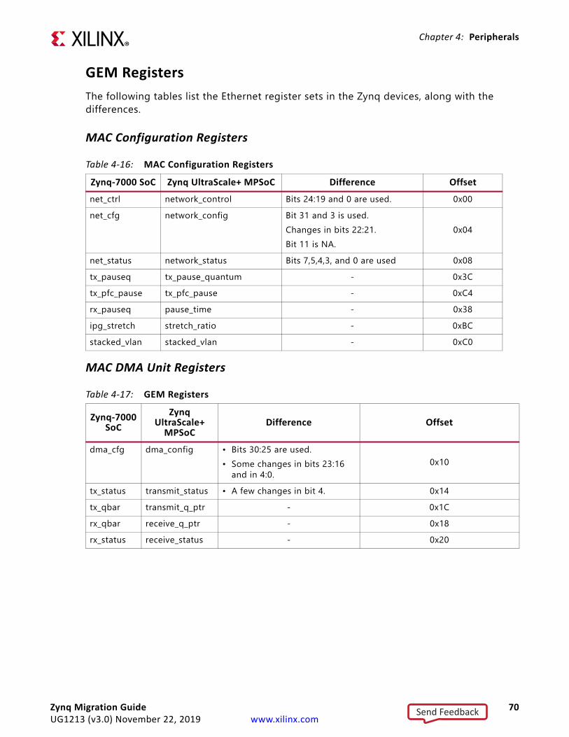
Chapter 4: Peripherals
GEM RegistersThe following tables list the Ethernet register sets in the Zynq devices, along with the differences.
MAC Configuration Registers
MAC DMA Unit Registers
Table 4-16: MAC Configuration RegistersZynq-7000 SoC Zynq UltraScale+ MPSoC Difference Offsetnet_ctrl network_control Bits 24:19 and 0 are used. 0x00net_cfg network_config Bit 31 and 3 is used.
Changes in bits 22:21. Bit 11 is NA.
0x04
net_status network_status Bits 7,5,4,3, and 0 are used 0x08tx_pauseq tx_pause_quantum - 0x3Ctx_pfc_pause tx_pfc_pause - 0xC4rx_pauseq pause_time - 0x38ipg_stretch stretch_ratio - 0xBCstacked_vlan stacked_vlan - 0xC0
Table 4-17: GEM Registers
Zynq-7000 SoC
Zynq UltraScale+
MPSoCDifference Offset
dma_cfg dma_config • Bits 30:25 are used.• Some changes in bits 23:16
and in 4:0. 0x10
tx_status transmit_status • A few changes in bit 4. 0x14tx_qbar transmit_q_ptr - 0x1Crx_qbar receive_q_ptr - 0x18rx_status receive_status - 0x20
Zynq Migration Guide 70UG1213 (v3.0) November 22, 2019 www.xilinx.com
Send Feedback

Chapter 4: Peripherals
GEM Interrupt Registers
GEM PHY Maintenance Register
GEM MAC Address Filtering and ID Match Registers
Table 4-18: GEM Interrupt Registers
Zynq-7000 SoCZynq
UltraScale+ MPSoC
Difference Offset
intr_status int_status • Bits 29:27,17:16,9 and 4 are used.
• Few changes in bit 6,0x24
intr_en int_enable • Bits 29:27,17:16 are used 0x28intr_dis int_disable • Bits 29:27,17:16 are used 0x2cintr_mask int_mask • Bits 29:26,17:16 are used 0x30wake_on_lan wol_register - 0xB8
Table 4-19: GEM PHY Maintenance Register
Zynq-7000 SoC Zynq UltraScale+ MPSoC Difference Offset
phy_maint phy_management • Changes in bits 29:28 0x34
Table 4-20: MAC Address Filtering and ID Match RegistersZynq-7000 SoC Zynq UltraScale+ MPSoC Difference Offset
hash_bot hash_bottom - 0x80hash_top hash_top - 0x84spec_addr1_bot spec_add1_bottom - 0x88spec_addr1_top spec_add1_top • Bit 16 is used. 0x8Cspec_addr2_bot spec_add2_bottom - 0x90spec_addr2_top spec_add2_top • Bits 29:24 and 16
are used. 0x94
spec_addr3_bot spec_add3_bottom - 0x98spec_addr3_top spec_add3_top • Bits 29:24 and 16
are used. 0x9C
spec_addr4_bot spec_add4_bottom - 0xA0spec_addr4_top spec_add4_top • Bits 29:24 and 16
are used. 0xA4
spec_addr1_mask_bot mask_add1_bottom - 0xC8spec_addr1_mask_top mask_add1_top - 0xCCtype_id_match1 spec_type1 - 0xA8
Zynq Migration Guide 71UG1213 (v3.0) November 22, 2019 www.xilinx.com
Send Feedback

Chapter 4: Peripherals
GEM Module ID Register
GEM Frame Statistics Registers
type_id_match2 spec_type2 - 0xACtype_id_match3 spec_type3 - 0xB0type_id_match4 spec_type4 - 0xB4
Table 4-21: GEM Module ID RegisterZynq-7000 SoC Zynq UltraScale+ MPSoC Difference Offset
module_id revision_req Changes in bits 31:16
0xFC
Table 4-22: GEM Frame Statistics Registers
Register Name Zynq-7000 SoCZynq
UltraScale+ MPSoC
Offset
frames_tx frames_txed_ok - 0x108broadcast_frames_tx broadcast_txed - 0x10Cmulti_frames_tx multicasi_txed - 0x110pause_frames_tx pause_frames_txed - 0x114frames_64b_tx frames_txed_64 - 0x118frames_65to127b_tx frames_txed_65 - 0x11Cframes_128to255b_tx frames_txed_128 - 0x120frames_256to511b_tx frames_txed_256 - 0x124frames_512to1023b_tx frames_txed_512 - 0x128frames_1024to1518b_tx frames_txed_1024 - 0x12Cdeferred_tx_frames deferred_frames - 0x148frames_rx frames_rxed_ok - 0x158bdcast_fames_rx broadcast_rxed - 0x15Cmulti_frames_rx multicasi_rxed - 0x160pause_rx pause_frames_rxed - 0x164frames_64b_rx frames_rxed_64 - 0x168frames_65to127b_rx frames_rxed_65 - 0x16Cframes_128to255b_rx frames_rxed_128 - 0x170frames_256to511b_rx frames_rxed_256 - 0x174frames_512to1023b_rx frames_rxed_512 - 0x178
Table 4-20: MAC Address Filtering and ID Match Registers (Cont’d)
Zynq-7000 SoC Zynq UltraScale+ MPSoC Difference Offset
Zynq Migration Guide 72UG1213 (v3.0) November 22, 2019 www.xilinx.com
Send Feedback

Chapter 4: Peripherals
GEM I/O InterfaceIn both the Zynq devices, the controller provides RGMII through the MIO pins and GMII through the EMIO.
GEM Bare-Metal DriversThe following table lists the Ethernet driver APIs.
frames_1024to1518b_rx frames_rxed_1024 - 0x17Cundersz_rx undersize_frames - 0x184oversz_rx excessive_rx_length - 0x188jab_rx rx_jabbers - 0x18Coctets_tx_bot octets_txed_bottom - 0x100octets_tx_top octets_txed_top - 0x104octets_rx_bot octets_rxed_bottom - 0x150octets_rx_top octets_rxed_top - 0x154tx_under_runs tx_underruns - 0x134fcs_errors fcs_errors - 0x190length_field_errors rx_length_errors - 0x194rx_symbol_errors rx_symbol_errors Few changes 0x198align_errors alignment_errors - 0x19Crx_resource_errors rx_resource_errors - 0x1A0rx_overrun_errors rx_overruns - 0x1A4
Table 4-23: Ethernet Driver APIsAPI Functional Description
XEmacPs_CfgInitialize Initialize a specific XEmacPs instance/driver.XEmacPs_Start Starts the Ethernet controller.XEmacPs_Stop Stops the Ethernet MAC.XEmacPs_Reset Resets the Ethernet MAC.XEmacPs_SetQueuePtr Sets the start address of the transmit/receive buffer
queue.XEmacPs_BdRingCreate Create and setup the BD list for the given DMA
channel.
Table 4-22: GEM Frame Statistics Registers (Cont’d)
Register Name Zynq-7000 SoCZynq
UltraScale+ MPSoC
Offset
Zynq Migration Guide 73UG1213 (v3.0) November 22, 2019 www.xilinx.com
Send Feedback

Chapter 4: Peripherals
XEmacPs_BdRingClone It can be called only when all BDs are in the free group such as they are immediately after initialization with XEmacPs_BdRingCreate().
XEmacPs_BdRingAlloc Reserve locations in the BD list.XEmacPs_BdRingUnAlloc Fully or partially undo an
XEmacPs_BdRingAlloc() operation.XEmacPs_BdRingToHw Enqueue a set of BDs to hardware that were
previously allocated by XEmacPs_BdRingAlloc().
XEmacPs_BdRingFromHwTx Returns a set of BD(s) that have been processed by hardware.
XEmacPs_BdRingFromHwRx Returns a set of BD(s) that have been processed by hardware.
XEmacPs_BdRingFree Frees a set of BDs that had been previously retrieved with XEmacPs_BdRingFromHw().
XEmacPs_BdRingCheck Check the internal data structures of the BD ring for the provided channel.
XEmacPs_BdSetRxWrap Set this bit to mark the last descriptor in the receive buffer descriptor list.
XEmacPs_BdSetTxWrap Sets this bit to mark the last descriptor in the transmit buffer descriptor list.
XEmacPs_SetMacAddress Sets the MAC address for this driver/device.XEmacPs_GetMacAddress Gets the MAC address for this driver/device.XEmacPs_SetHash Sets 48-bit MAC addresses in hash table.XEmacPs_DeleteHash Delete 48-bit MAC addresses in hash table.XEmacPs_ClearHash Clears the Hash registers for the mac address
pointed by AddressPtr.XEmacPs_GetHash Gets the Hash address for this driver/device.XEmacPs_SetTypeIdCheck Sets the Type ID match for this driver/device.XEmacPs_SetOptions Sets options for the driver/device.XEmacPs_ClearOptions Clears options for the driver/deviceXEmacPs_GetOptions Gets current option settingsXEmacPs_SendPausePacket Sends a pause packetXEmacPs_GetOperatingSpeed Gets the current operating link speed.XEmacPs_SetOperatingSpeed Sets the current operating link speed. XEmacPs_SetMdioDivisor Sets the MDIO clock divisor.XEmacPs_PhyRead Reads the current value of the PHY register
indicated by the PhyAddress and the RegisterNum parameters.
Table 4-23: Ethernet Driver APIs (Cont’d)
API Functional Description
Zynq Migration Guide 74UG1213 (v3.0) November 22, 2019 www.xilinx.com
Send Feedback

Chapter 4: Peripherals
GEM Linux DriversUse the Zynq UltraScale+ MPSoC device equivalent Linux driver. No change is required in the software application code.
GEM Device Tree BindingThe following table lists the GEM device tree binding information.
XEmacPs_PhyWrite Writes data to the specified PHY register.XEmacPs_DMABLengthUpdate Updates the Burst length in the DMACR register.XEmacPs_ConfigTable Configuration table that specifies the
configuration of ethernet devices in the system.XEmacPs_ResetHw Performs the reset sequence to the given emacps
interface by configuring the appropriate control bits in the emacps-specifc registers.
XEmacPs_SetHandler Install an asynchronous handler function for the given HandlerType.
XEmacPs_IntrHandler Master interrupt handler for EMAC driver. XEmacPs_LookupConfig Lookup the device configuration based on the
unique device ID.
Table 4-24: GEM Device Tree BindingInformation Zynq-7000 SoC Zynq UltraScale+ MPSoC
GEM #0 GEM #1 GEM #0 GEM #1 GEM #2 GEM #3Compatible “cdns,uart-g
em”, “cdns,uart”
“cdns,uart-gem”, “cdns,uart”
“xlnx,zynqmp-gem”
“xlnx,zynqmp-gem”
“xlnx,zynqmp-gem”
“xlnx,zynqmp-gem”
Interrupt Number
22 45 57 59 61 63
Physical baseaddress and size ofregister
0xe000b000 0xe000c000 0xff0b0000 0xff0c0000 0xff0d0000 0xff0e0000
Input clocks clkc 30, clkc 13
clkc 31, clkc 14
“pclk”, “clk”, “uart_clk”
“pclk”, “clk”, “uart_clk”
“pclk”, “clk”, “uart_clk”
“pclk”, “clk”, “uart_clk”
PHY type “marvell,88e1116r”0x7
-- -- -- -- rimming-id0x21
GPIO reset -- -- -- -- -- --IOMMUs -- -- smmu 0x874 smmu 0x875 smmu 0x876 smmu 0x877
Table 4-23: Ethernet Driver APIs (Cont’d)
API Functional Description
Zynq Migration Guide 75UG1213 (v3.0) November 22, 2019 www.xilinx.com
Send Feedback

Chapter 4: Peripherals
USB ControllerThe Zynq-7000 SoC also has two USB 2.0 controllers and each controller can be configured and controlled independently.
The Zynq UltraScale+ MPSoC device USB 2.0/3.0 controller consists of two independent dual-role device (DRD) controllers.
Both can be individually configured to work as host or device at any given time. These controllers provide simultaneous operation of the USB 2.0 and USB 3.0 interfaces (in host mode only).
USB Architectural DifferencesThe following table lists the key architectural differences between the USB controller in the Zynq devices.
The following block diagram shows the USB 2.0/3.0 controller in the Zynq UltraScale+ MPSoC device.
Table 4-25: USB Controller DifferencesSl. Zynq-7000 SoC Zynq UltraScale+ MPSoC
1. Two USB 2.0 controllers. Two USB 2.0/3.0 controllers.2. Does not support hibernation mode. Supports hibernation mode.3. Support for 32-bit address space. Support for 44-bit address space.4. Internal DMA engine utilizes the 32-bit AHB
master interface.Internal DMA engine utilizes the 32-bit AXI master interface.
X-Ref Target - Figure 4-11
Figure 4-11: Zynq UltraScale+ MPSoC USB 3.0 Block Controller
Zynq Migration Guide 76UG1213 (v3.0) November 22, 2019 www.xilinx.com
Send Feedback

Chapter 4: Peripherals
USB Supported ModesThe operation modes supported by USB 2.0/3.0 are the same in both Zynq devices. The different USB modes supported are, as follows:
° Host mode° Device mode ° On-the-Go (OTG) host/device selection
USB ResetsThe following sections list the different types of resets associated with the USB controller in the Zynq devices.
Zynq-7000 SoC Device
Each controller has its own reset input from the PS reset module. There are several different types of resets associated with the USB controller.
° Controller resets
° PS Reset System (full controller reset)
° usb.USBCMD [RST] bit (partial controller reset useful for OTG)
° ULPI PHY Reset
° A PS GPIO signal can be used to reset the external PHY
Zynq UltraScale+ MPSoC Device
• Controller resets:
° In register DCTL[30], set the CsftRst field to 1.
° Set the CORESOFTRESET bit GCTL[11] in Global core control register. • Device resets:
° Set GCTL[13:12] (PrtCapDir) to 2'b01 (host mode).
° Set GCTL[13:12] (PrtCapDir) to 2'b10 (device mode).
° Reset the host using USB command register LHCRST (light host reset) and USBCMD.HCRESET.
• UTMI PHY reset
° Reset the PHY using GUSB2PHYCFG UTMI PHY soft reset by bit PHYSOFTRST or GUSB3PIPECTL bit.
Zynq Migration Guide 77UG1213 (v3.0) November 22, 2019 www.xilinx.com
Send Feedback

Chapter 4: Peripherals
USB Configuration and Data Flow To configure USB 3.0 as USB 2.0 in Zynq UltraScale+ MPSoC devices, See this link to the “USB 2.0/3.0 Host, Device, and OTG Controller” chapter in the Zynq UltraScale+ MPSoC Technical Reference Manual (UG1085) [Ref 10].
USB RegistersSee the Zynq UltraScale+ MPSoC Devices USB3 register base at MPSoC___USB3_Registers [Ref 16].
USB I/O InterfaceThe controller has multiple interfaces including the main UltraScale low pin interface (ULPI) interface. The following are the various I/O interfaces in the Zynq-7000 SoC device and Zynq UltraScale+ MPSoC device.
Zynq-7000 SoC Device
• The controller has multiple I/O interfaces including the main ULPI that interfaces via MIO to the external PHY and the port indicator and power signals via EMIO. The routing of the ULPI through the MIO must be programmed. The routing of the signals through the EMIO is always available to logic in the PL that can route these signals to the SelectIO™ pins.
• ULPI using MIO: The controller interfaces to the external ULPI PHY using 12 MIO pins: eight data I/Os, direction input, control input, clock input, and a stop output.
• Port Indicator and Power Pins using EMIO: The USB port indicator outputs, power select output, and power fault input signals are routed through the EMIO to the SelectIO pins in the PL and external board logic.
Zynq UltraScale+ MPSoC
USB2 UTMI+ low pin interface (ULPI) is not supported in the EMIO.
Protocol StackAlso, the protocol stack used in the Zynq-7000 SoC and the Zynq MPSoC devices are different.The Zynq-7000 SoC device uses the EHCI stack. It is initialized by means of enabling the EHCI stack in the kernel configuration. This invokes the following:
ehci_platform_probe () in the usb/host/ ehci-platform.c
The Zynq UltraScale+ MPSoC uses the xHCI stack. It is initialized by enabling xHCI stack in the kernel configuration. This invokes the following:
Zynq Migration Guide 78UG1213 (v3.0) November 22, 2019 www.xilinx.com
Send Feedback

Chapter 4: Peripherals
xhci_plat_probe() in the usb/host/xhci-plat.c
USB Bare-Metal DriversThe following table specifies the USB driver APIs in the Zynq devices, and the different steps to use between devices.
Table 4-26: USB Bare-Metal Driver DifferencesZynq-7000 SoC Zynq UltraScale+ MPSoC Difference
XusbPs_CfgInitialize XUsbPsu_CfgInitialize In the Zynq-7000 SoC device:1. Copy the config structure.2. Check if the user provided a
non-NULL base address.• If so, overwrite the base
address in the configuration structure.
3. Initialize the XUsbPs structure to default values.
In the Zynq UltraScale+ MPSoC device: 1. Copy the config structure.2. Initialize core.3. Map USB and Physical
EndpointsXusbPs_DeviceReset - -XusbPs_Reset - -XusbPs_Suspend - -XusbPs_Resume - -XusbPs_RequestHostResume - -XusbPs_SetDeviceAddress XUsbPsu_SetDeviceAddress In the Zynq-7000 SoC device:
1. Check address range validity.
2. Set the address register.In the Zynq UltraScale+ MPSoC device, it checks whether it is already configured.• Set the device configuration
register.• The device checks the
address to change the state.- XUsbPsu_Wait_Clear_Timeout -- XUsbPsu_Wait_Set_Timeout -- XUsbPsu_SetMode -- XUsbPsu_PhyReset -
Zynq Migration Guide 79UG1213 (v3.0) November 22, 2019 www.xilinx.com
Send Feedback

Chapter 4: Peripherals
- XUsbPsu_EventBuffersSetup -- XUsbPsu_EventBuffersReset -- XUsbPsu_ReadHwParams -- XUsbPsu_CoreInit -- XUsbPsu_EnableIntr -- XUsbPsu_DisableIntr -- XUsbPsu_Start -- XUsbPsu_Stop -- XUsbPsu_SetTestMode -- XUsbPsu_GetLinkState -- XUsbPsu_SetLinkState -- XUsbPsu_SetSpeed -
XusbPs_ConfigureDevice - -XusbPs_EpBufferSend - -XusbPs_EpBufferSendWithZLT - -XusbPs_EpQueueRequest - -XusbPs_EpBufferReceive - -XusbPs_EpBufferRelease - -XusbPs_EpSetHandler - -XusbPs_EpPrime - -XusbPs_EpGetSetupData - -XusbPs_EpListInit - -XusbPs_dQHInit - -XusbPs_dTDInit - -XUsbPs_dTDAttachBuffer - -XUsbPs_dQHSetMaxPacketLenISO - -XUsbPs_ReconfigureEp - -XUsbPs_dQHReinitEp - -XusbPs_dTDReinitEp - -
- XUsbPsu_GetEpParams -- XUsbPsu_EpGetTransferIndex -- XUsbPsu_SendEpCmd -- XUsbPsu_StartEpConfig -- XUsbPsu_SetEpConfig -- XUsbPsu_SetXferResource -
Table 4-26: USB Bare-Metal Driver Differences (Cont’d)
Zynq-7000 SoC Zynq UltraScale+ MPSoC Difference
Zynq Migration Guide 80UG1213 (v3.0) November 22, 2019 www.xilinx.com
Send Feedback

Chapter 4: Peripherals
- XUsbPsu_EpEnable -- XUsbPsu_EpDisable -- XUsbPsu_EnableControlEp -- XUsbPsu_InitializeEps -- XUsbPsu_StopTransfer -- XUsbPsu_ClearStalls -- XUsbPsu_EpBufferSend -- XUsbPsu_EpBufferRecv -- XUsbPsu_EpSetStall -- XUsbPsu_EpClearStall -- XUsbPsu_SetEpHandler -- XUsbPsu_IsEpStalled -- XUsbPsu_EpXferComplete -
XusbPs_ConfigTable XUsbPsu_ConfigTable • Zynq UltraScale+ MPSoC devices has Device ID information.
XusbPs_ResetHw - -XusbPs_IntrHandler XUsbPsu_IntrHandler In the Zynq-7000 SoC device:
1. Handle controller related interrupts.
2. Clear the interrupt status register.
3. Respond to host's IN request.4. Handle general interrupts.5. Handle Endpoint interrupts.• In the Zynq UltraScale+
MPSoC device, it processes the events if the event count is greater than zero, then: ° Masks the interrupt° Processes the event° Unmasks the interrupt
XusbPs_IntrSetHandler - -XusbPs_IntrHandleTX - -XusbPs_IntrHandleRX - -XusbPs_IntrHandleReset - -XusbPs_IntrHandleEp0Setup - -
- XUsbPsu_EpInterrupt -- XUsbPsu_DisconnectIntr -
Table 4-26: USB Bare-Metal Driver Differences (Cont’d)
Zynq-7000 SoC Zynq UltraScale+ MPSoC Difference
Zynq Migration Guide 81UG1213 (v3.0) November 22, 2019 www.xilinx.com
Send Feedback
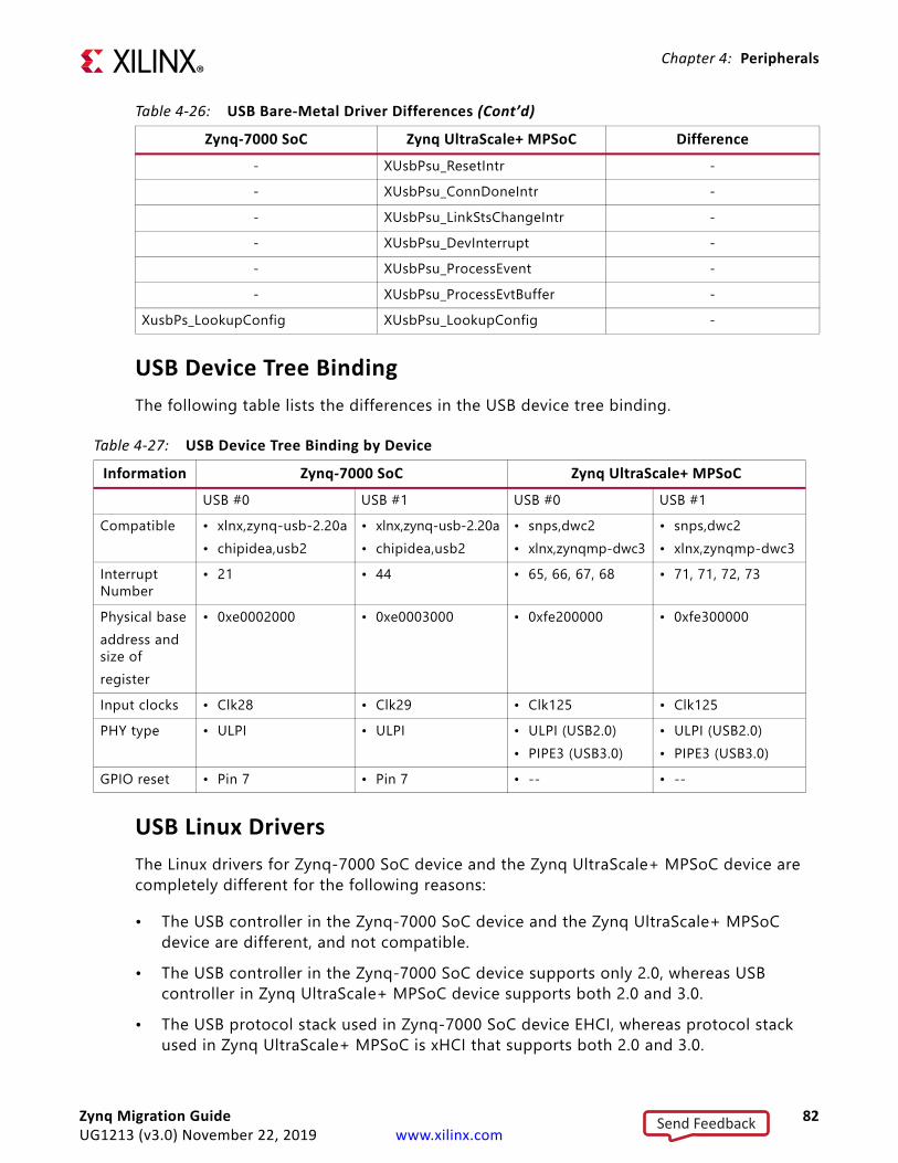
Chapter 4: Peripherals
USB Device Tree BindingThe following table lists the differences in the USB device tree binding.
USB Linux DriversThe Linux drivers for Zynq-7000 SoC device and the Zynq UltraScale+ MPSoC device are completely different for the following reasons:
• The USB controller in the Zynq-7000 SoC device and the Zynq UltraScale+ MPSoC device are different, and not compatible.
• The USB controller in the Zynq-7000 SoC device supports only 2.0, whereas USB controller in Zynq UltraScale+ MPSoC device supports both 2.0 and 3.0.
• The USB protocol stack used in Zynq-7000 SoC device EHCI, whereas protocol stack used in Zynq UltraScale+ MPSoC is xHCI that supports both 2.0 and 3.0.
- XUsbPsu_ResetIntr -- XUsbPsu_ConnDoneIntr -- XUsbPsu_LinkStsChangeIntr -- XUsbPsu_DevInterrupt -- XUsbPsu_ProcessEvent -- XUsbPsu_ProcessEvtBuffer -
XusbPs_LookupConfig XUsbPsu_LookupConfig -
Table 4-26: USB Bare-Metal Driver Differences (Cont’d)
Zynq-7000 SoC Zynq UltraScale+ MPSoC Difference
Table 4-27: USB Device Tree Binding by DeviceInformation Zynq-7000 SoC Zynq UltraScale+ MPSoC
USB #0 USB #1 USB #0 USB #1Compatible • xlnx,zynq-usb-2.20a
• chipidea,usb2• xlnx,zynq-usb-2.20a• chipidea,usb2
• snps,dwc2• xlnx,zynqmp-dwc3
• snps,dwc2• xlnx,zynqmp-dwc3
Interrupt Number
• 21 • 44 • 65, 66, 67, 68 • 71, 71, 72, 73
Physical baseaddress and size ofregister
• 0xe0002000 • 0xe0003000 • 0xfe200000 • 0xfe300000
Input clocks • Clk28 • Clk29 • Clk125 • Clk125PHY type • ULPI • ULPI • ULPI (USB2.0)
• PIPE3 (USB3.0)• ULPI (USB2.0)• PIPE3 (USB3.0)
GPIO reset • Pin 7 • Pin 7 • -- • --
Zynq Migration Guide 82UG1213 (v3.0) November 22, 2019 www.xilinx.com
Send Feedback

Chapter 4: Peripherals
Because the two USB controllers are completely different, the sequence of operations change drastically, as shown in the following table.
Table 4-28: USB Linux DriversDescription Zynq-7000 SoC Zynq UltraScale+ MPSoC
Initialize the core 1 Disable the controller.2 Create a HCD instance with all
hook functions, such as:° ehci_irq° ehci_setup° ehci_run° ehci_stop° ehci_shutdown° ehci_urb_enqueueu° ehci_urb_dequeue° ehci_endpoint_disable° ehci_endpoint_reset° ehci_get_frame° ehci_hub_status_data° ehci_hub_control
3 Get base address, interrupt id.4 Register to EHCI stack5 Register to HCD core
1 Get the platform resources2 Set the driver config variables.3 Allocate the event buffers.4 Set the hardware parameters.5 Check the USB3 version.6 USB2.0 core configuration.7 Issue device software reset.8 Configure the USB PHY interface.9 Allocate scratch buffers.10 Setup scratch buffers.11 Setup event buffers.12 Initialize core mode.13 Setup code mode.
Get the driver data - 1 Suspend driver mode.2 Shutdown PHY. PHY exits.
Resume Not applicable USB PHY initializationLock interruptsSetup event buffersSetup driver modeUnlock interrupts
Remove the core Unregister from HCD coreUnregister from EHCI stack
Exit core modeCleanup event buffersFree event buffersPHY suspendPHY power offCore exit
Zynq Migration Guide 83UG1213 (v3.0) November 22, 2019 www.xilinx.com
Send Feedback

Chapter 4: Peripherals
General Purpose I/OThe general purpose I/O (GPIO) peripheral provides software with observation and control of device pins through the MIO module. It also provides access to inputs from the programmable logic (PL) and outputs to the PL through the EMIO interface.
GPIO Architectural DifferencesIn the Zynq-7000 SoC device, there are the following:
° 54 GPIO signals for device pins (routed through the MIO multiplexer) and 192 GPIO signals between the PS and PL using the EMIO interface.
° In 192 GPIO signals, 64 are inputs, 128 are outputs (64 true outputs and 64 output enables).
° Device GPIO organized into four banks of registers that group related interface signals.
In the Zynq UltraScale+ MPSoC device, there are the following:
° 78 GPIO signals for device pins which are routed through the MIO multiplexer and 288 GPIO signals between the PS and PL through the EMIO interface.
° In 288 GPIO signals, 96 are inputs and 192 are outputs (96 true outputs and 96 output enables).
° Device GPIO organized into six banks of registers that group related interface signals.
Zynq Migration Guide 84UG1213 (v3.0) November 22, 2019 www.xilinx.com
Send Feedback

Chapter 4: Peripherals
The following table shows different banks and pins controlled by GPIO in both the Zynq devices.
X-Ref Target - Figure 4-12
Figure 4-12: Zynq UltraScale+ MPSoC Device GPIO Registers
Table 4-29: GPIO Banks and PinsBank Zynq UltraScale+ MPSoC Zynq-7000 SoC
Bank0 MIO pins[25:0] MIO pins[31:0]Bank1 MIO pins[51:26] MIO pins[53:32]Bank2 MIO pins[77:52] EMIO pins[31:0]Bank3 EMIO pins[31:0] EMIO pins[63:32]Bank4 EMIO pins[63:32] -Bank5 EMIO pins[95:64] -
Zynq Migration Guide 85UG1213 (v3.0) November 22, 2019 www.xilinx.com
Send Feedback

Chapter 4: Peripherals
GPIO ClockIn the Zynq-7000 SoC device, the controller is clocked by the CPU_1x clock from the APB interface.
• All outputs and input sampling is done using the CPU_1x clock. • For power management, clock gating can be employed on the GPIO controller clock
using slcr.APER_CLK_CTRL[GPIO_CPU_1XCLKACT].
In the Zynq UltraScale+ MPSoC device, the controller is clocked by the CPU_1x clock from the APB interface.
• All outputs and input sampling is done using the CPU_1x clock. • For power management, clock gating can be employed on the GPIO controller clock
using the slcr.APER_CLK_CTRL[GPIO_CPU_1XCLKACT] bit.
GPIO ResetIn the Zynq-7000 SoC device, the controller is reset by the slcr.GPIO_RST_CTRL [GPIO_CPU1X_RST] bit. This reset only affects the bus interface, not the controller logic itself.
In the Zynq UltraScale+ MPSoC device, the controller is reset by the slcr.GPIO_RST_CTRL [GPIO_CPU1X_RST] bit. This reset only affects the bus interface and not the controller logic). GPIO can be reset in this device using RST_LPD_IOU2 register. The RST_LPD_IOU2 is a part of APB control registers (CRL_APB).
Zynq Migration Guide 86UG1213 (v3.0) November 22, 2019 www.xilinx.com
Send Feedback

Chapter 4: Peripherals
GPIO Configuration and Data Flow The following diagram shows the GPIO configuration in the Zynq devices. The steps that differ in Zynq UltraScale+ MPSoC device from the Zynq-7000 SoC device are highlighted in red.
GPIO RegistersThe following table lists GPIO registers in both the Zynq devices with their differences.
X-Ref Target - Figure 4-13
Figure 4-13: GPIO Configuration and Data Flow (Zynq-7000 SoC Devices Differences in Red)
Table 4-30: GPIO Data Control RegistersRegister Name Zynq-7000 SoC Zynq UltraScale + MPSoC Offset
MASK_DATA_0_LSW MASK_DATA_0_LSW - 0x00MASK_DATA_0_MSW MASK_DATA_0_MSW • In the Zynq UltraScale+
MPSoC device, bits[31:26] and bits[15:10] are unused.
0x04
MASK_DATA_1_LSW MASK_DATA_1_LSW - 0x08MASK_DATA_1_MSW MASK_DATA_1_MSW • In the Zynq UltraScale+
MPSoC device, bits[31:26] and bits[15:10] are unused.
0x0C
MASK_DATA_2_LSW MASK_DATA_2_LSW - 0x10MASK_DATA_2_MSW MASK_DATA_2_MSW • In the Zynq UltraScale+
MPSoC device, bits[31:26] and bits[15:10] are unused.
0x14
MASK_DATA_3_LSW MASK_DATA_3_LSW - 0x18MASK_DATA_3_MSW MASK_DATA_3_MSW - 0x1C
- MASK_DATA_4_LSW - 0x20
Zynq Migration Guide 87UG1213 (v3.0) November 22, 2019 www.xilinx.com
Send Feedback
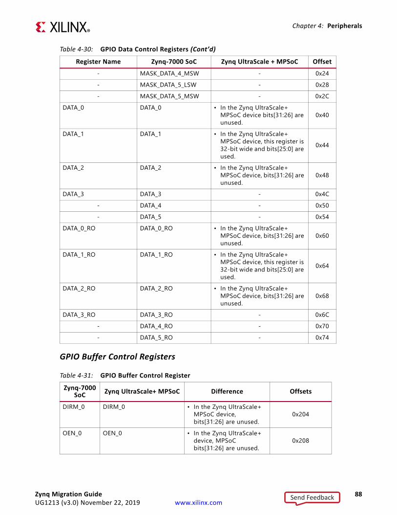
Chapter 4: Peripherals
GPIO Buffer Control Registers
- MASK_DATA_4_MSW - 0x24- MASK_DATA_5_LSW - 0x28- MASK_DATA_5_MSW - 0x2C
DATA_0 DATA_0 • In the Zynq UltraScale+ MPSoC device bits[31:26] are unused.
0x40
DATA_1 DATA_1 • In the Zynq UltraScale+ MPSoC device, this register is 32-bit wide and bits[25:0] are used.
0x44
DATA_2 DATA_2 • In the Zynq UltraScale+ MPSoC device, bits[31:26] are unused.
0x48
DATA_3 DATA_3 - 0x4C- DATA_4 - 0x50- DATA_5 - 0x54
DATA_0_RO DATA_0_RO • In the Zynq UltraScale+ MPSoC device, bits[31:26] are unused.
0x60
DATA_1_RO DATA_1_RO • In the Zynq UltraScale+ MPSoC device, this register is 32-bit wide and bits[25:0] are used.
0x64
DATA_2_RO DATA_2_RO • In the Zynq UltraScale+ MPSoC device, bits[31:26] are unused.
0x68
DATA_3_RO DATA_3_RO - 0x6C- DATA_4_RO - 0x70- DATA_5_RO - 0x74
Table 4-31: GPIO Buffer Control RegisterZynq-7000
SoC Zynq UltraScale+ MPSoC Difference Offsets
DIRM_0 DIRM_0 • In the Zynq UltraScale+ MPSoC device, bits[31:26] are unused.
0x204
OEN_0 OEN_0 • In the Zynq UltraScale+ device, MPSoC bits[31:26] are unused.
0x208
Table 4-30: GPIO Data Control Registers (Cont’d)
Register Name Zynq-7000 SoC Zynq UltraScale + MPSoC Offset
Zynq Migration Guide 88UG1213 (v3.0) November 22, 2019 www.xilinx.com
Send Feedback

Chapter 4: Peripherals
GPIO Interrupt control Registers,
DIRM_1 DIRM_1 • In Zynq UltraScale+ MPSoC this register is 32-bit wide and bits[25:0] are used.
0x244
OEN_1 OEN_1 • In the Zynq UltraScale+ MPSoC device, this register is 32-bit wide and bits[25:0] are used.
0x248
DIRM_2 DIRM_2 • In the Zynq UltraScale+ MPSoC device, bits[31:26] are unused.
0x284
OEN_2 OEN_2 • In the Zynq UltraScale+ MPSoC device, bits[31:26] are unused.
0x288
DIRM_3 DIRM_3 - 0x2C4OEN_3 OEN_3 - 0x2C8
- DIRM_4 - 0x304- OEN_4 - 0x308- DIRM_5 - 0x344- OEN_5 - 0x348
Table 4-32: GPIO Interrupt Control Registers
Zynq-7000 SoC Zynq UltraScale+ MPSoC
Differences (1,2,3,4) Offset
INT_MASK_0 INT_MASK_0 1 0x20CINT_EN_0 INT_EN_0 1 0x210INT_DIS_0 INT_DIS_0 1 0x214INT_STAT_0 INT_STAT_0 1 0x218INT_TYPE_0 INT_TYPE_0 1 0x21CINT_POLARITY_0 INT_POLARITY_0 1,2 0x220
Notes: 1. In the Zynq UltraScale+ MPSoC device, INT_[MASK,EN,DIS,STAT,TYPE,POLARITY,ANY]_0 register
bits[31:26] are unused.2. 2. In the Zynq UltraScale+ MPSoC device, INT_[MASK,EN,DIS,STAT,TYPE,POLARITY,ANY]_0
register bits[31:26] are unused.3. 3. In the Zynq UltraScale+ MPSoC device, INT_[MASK,EN,DIS,STAT,TYPE,POLARITY,ANY]_2 register
bits[31:26] are unused.4. 4. In the Zynq UltraScale+ MPSoC device, INT_[MASK,EN,DIS,STAT,TYPE,POLARITY,ANY]_3 register
bits[31:26] are unused.
Table 4-31: GPIO Buffer Control Register (Cont’d)
Zynq-7000 SoC Zynq UltraScale+ MPSoC Difference Offsets
Zynq Migration Guide 89UG1213 (v3.0) November 22, 2019 www.xilinx.com
Send Feedback

Chapter 4: Peripherals
INT_ANY_0 INT_ANY_0 1,2 0x224INT_MASK_1 INT_MASK_1 1,2 0x24CINT_EN_1 INT_EN_1 1,2 0x250INT_DIS_1 INT_DIS_1 1,2 0x254INT_STAT_1 INT_STAT_1 1,2 0x258INT_TYPE_1 INT_TYPE_1 1,2 0x25CINT_POLARITY_1 INT_POLARITY_1 1,2 0x260INT_ANY_1 INT_ANY_1 1,2 0x264INT_MASK_2 INT_MASK_2 1,3 0x28CINT_EN_2 INT_EN_2 1,3 0x290INT_DIS_2 INT_DIS_2 1,3 0x294INT_STAT_2 INT_STAT_2 1,3 0x298INT_TYPE_2 INT_TYPE_2 1,3 0x29CINT_POLARITY_2 INT_POLARITY_2 1,3 0x2A0INT_ANY_2 INT_ANY_2 1,3 0x2A4INT_MASK_3 INT_MASK_3 1,4 0x2CCINT_EN_3 INT_EN_3 1,4 0x2D0INT_DIS_3 INT_DIS_3 1,4 0x2D4INT_STAT_3 INT_STAT_3 1,4 0x2D8INT_TYPE_3 INT_TYPE_3 1,4 0x2DCINT_POLARITY_3 INT_POLARITY_3 1,4 0x2E0INT_ANY_3 INT_ANY_3 1,4 0x2E4
- INT_MASK_4 - 0x30C- INT_EN_4 - 0x310- INT_DIS_4 - 0x314- INT_STAT_4 - 0x318- INT_TYPE_4 - 0x31C
Table 4-32: GPIO Interrupt Control Registers (Cont’d)
Zynq-7000 SoC Zynq UltraScale+ MPSoC
Differences (1,2,3,4) Offset
Notes: 1. In the Zynq UltraScale+ MPSoC device, INT_[MASK,EN,DIS,STAT,TYPE,POLARITY,ANY]_0 register
bits[31:26] are unused.2. 2. In the Zynq UltraScale+ MPSoC device, INT_[MASK,EN,DIS,STAT,TYPE,POLARITY,ANY]_0
register bits[31:26] are unused.3. 3. In the Zynq UltraScale+ MPSoC device, INT_[MASK,EN,DIS,STAT,TYPE,POLARITY,ANY]_2 register
bits[31:26] are unused.4. 4. In the Zynq UltraScale+ MPSoC device, INT_[MASK,EN,DIS,STAT,TYPE,POLARITY,ANY]_3 register
bits[31:26] are unused.
Zynq Migration Guide 90UG1213 (v3.0) November 22, 2019 www.xilinx.com
Send Feedback

Chapter 4: Peripherals
GPIO I/O InterfaceIn both Zynq devices GPIO signal are routed through MIO and some GPIO signals between the PS and PL through the EMIO interface.
GPIO Bare-Metal DriversThe GPIO bare-metal driver for the Zynq devices is the same. The following table lists of the GPIO driver APIs.
- INT_POLARITY_4 - 0x320- INT_ANY_4 - 0x324- INT_MASK_5 - 0x34C- INT_EN_5 - 0x350- INT_DIS_5 - 0x354- INT_STAT_5 - 0x358- INT_TYPE_5 - 0x35C- INT_POLARITY_5 - 0x360- INT_ANY_5 - 0x364
Table 4-33: GPIO APIs API Functional Description
XGpioPs_CfgInitialize Initializes a GPIO instance/driver.XGpioPs_Read Reads the data register of the specified GPIO bank.XGpioPs_ReadPin Reads data from the specified pin.XGpioPs_Write Writes to the data register of the specified GPIO
bank.XGpioPs_WritePin Writes data to the specified pin.XGpioPs_SetDirection Sets the direction of the pins of the specified GPIO
bank.
Table 4-32: GPIO Interrupt Control Registers (Cont’d)
Zynq-7000 SoC Zynq UltraScale+ MPSoC
Differences (1,2,3,4) Offset
Notes: 1. In the Zynq UltraScale+ MPSoC device, INT_[MASK,EN,DIS,STAT,TYPE,POLARITY,ANY]_0 register
bits[31:26] are unused.2. 2. In the Zynq UltraScale+ MPSoC device, INT_[MASK,EN,DIS,STAT,TYPE,POLARITY,ANY]_0
register bits[31:26] are unused.3. 3. In the Zynq UltraScale+ MPSoC device, INT_[MASK,EN,DIS,STAT,TYPE,POLARITY,ANY]_2 register
bits[31:26] are unused.4. 4. In the Zynq UltraScale+ MPSoC device, INT_[MASK,EN,DIS,STAT,TYPE,POLARITY,ANY]_3 register
bits[31:26] are unused.
Zynq Migration Guide 91UG1213 (v3.0) November 22, 2019 www.xilinx.com
Send Feedback

Chapter 4: Peripherals
XGpioPs_SetDirectionPin Sets the direction of the specified pin.XGpioPs_GetDirection Gets the direction of the pins of the specified GPIO
bank.XGpioPs_GetDirectionPin Gets the direction of the specified pin.XGpioPs_SetOutputEnable Sets the Output Enable of the pins of the specified
GPIO bank.XGpioPs_SetOutputEnablePin Sets the Output Enable of the specified pin.XGpioPs_GetOutputEnable Gets the Output Enable status of the pins of the
specified GPIO bank.XGpioPs_GetOutputEnablePin Gets the Output Enable status of the specified pin.XGpioPs_GetBankPin Gets the bank number and the Pin number in the
bank, for the given Pin Number in the GPIO device.XGpioPs_ConfigTable This table contains configuration information for
each GPIO device in the system.XGpioPs_ResetHw Resets the GPIO module by writing reset values to
all registersXGpioPs_IntrEnable Enables the interrupts for the specified pins in the
specified bank.XGpioPs_IntrEnablePin Enables the interrupt for the specified pin.XGpioPs_IntrDisable Disables the interrupts for the specified pins in the
specified bank.XGpioPs_IntrDisablePin Disables the interrupts for the specified pin.XGpioPs_IntrGetEnabled Returns the interrupt enable status for a bank.XGpioPs_IntrGetEnabledPin Returns whether interrupts are enabled for the
specified pin.XGpioPs_IntrGetStatus Returns interrupt status read from Interrupt Status
Register.XGpioPs_IntrGetStatusPin Returns interrupt enable status of the specified pin.XGpioPs_IntrClear Clears pending interrupt(s) with the provided
mask.XGpioPs_IntrClearPin Clears the specified pending interrupt. XGpioPs_SetIntrType Sets the Interrupt Type, Interrupt Polarity, and
Interrupt on any specified GPIO bank pins.XGpioPs_GetIntrType Gets the Interrupt Type, Interrupt Polarity, and
Interrupt on any specified GPIO bank pins.XGpioPs_SetIntrTypePin Sets the IRQ Type of a single GPIO pin.XGpioPs_GetIntrTypePin Returns the IRQ Type of a given GPIO pin.XGpioPs_SetCallbackHandler Sets the status callback function.XGpioPs_IntrHandler Interrupt handler for GPIO interrupts.
Table 4-33: GPIO APIs (Cont’d)
API Functional Description
Zynq Migration Guide 92UG1213 (v3.0) November 22, 2019 www.xilinx.com
Send Feedback

Chapter 4: Peripherals
GPIO Linux DriversUse the Zynq UltraScale+ MPSoC device equivalent Linux driver. No change is required in the software application code.
GPIO Device Tree BindingThe following table list the GPIO device tree binding.
Multiplexed I/OThe Multiplexed I/O (MIO) is fundamental to the I/O peripheral connections due to the limited number of MIO pins.
° Software programs the routing of the I/O signals to the MIO pins.
° The I/O peripheral signals can also be routed to the PL (including PL device pins) through the EMIO interface. This is useful to gain access to more device pins (PL pins) and to allow an I/O peripheral controller to interface to user logic in the PL.
The MIO module allows you to configure the PS pin-out as required.
XGpioPs_SelfTest Runs a self-test on the GPIO driver/device.XGpioPs_LookupConfig Looks for the device configuration based on the
unique device ID.
Table 4-34: GPIO Device Binding TreeInformation Zynq-7000 SoC Zynq UltraScale+ MPSoC
Compatible xlnx,zynq-gpio-1.0 xlnx,zynq-gpio-1.0Clock specifier &clkc 42 -Interrupt controller - -Interrupt parent &intc -Interrupt number 0 20 4 -gpio controller - -Physical base address and size of register
0xE000A000 0X1000
0xFF0A00000X10000
#gpio-cells 2 -#interrupt-cells 2 -
Table 4-33: GPIO APIs (Cont’d)
API Functional Description
Zynq Migration Guide 93UG1213 (v3.0) November 22, 2019 www.xilinx.com
Send Feedback

Chapter 4: Peripherals
° In the Zynq-7000 SoC device, 54 (34, 44, or 54) of the processing system I/Os as MIO.
° In the Zynq UltraScale+ MPSoC device, uses 78 of the processing system I/Os as MIOs.
The following diagram shows an overview of MIO and the external multiplexed I/O (EMIO) in the Zynq UltraScale+ MPSoC device.
Routing CapabilitiesThe following table shows the routing capabilities for each I/O peripheral in both the Zynq UltraScale+ MPSoC device and the Zynq-7000 SoC device.
X-Ref Target - Figure 4-14
Figure 4-14: Multiplexed I/O
Table 4-35: Routing Capabilities in I/O Peripherals
Interface Type Zynq-7000 SoC MIO Access
Zynq UltraScale+ MPSoC MIO
AccessZynq-7000 SoC EMIO Access
Zynq UltraScale+ MPSoC EMIO
AccessGigaE0 Yes Yes Yes YesGigaE1 Yes Yes Yes Yes
Zynq Migration Guide 94UG1213 (v3.0) November 22, 2019 www.xilinx.com
Send Feedback

Chapter 4: Peripherals
Multiplexed RegistersThe following table lists the MIO registers.
Multiplexed I/O Routing Capabilities
SDIO0 Yes Yes Yes YesSDIO1 Yes Yes Yes YesUSB0 Yes Yes No NoUSB1 Yes Yes No NoSPI0 Yes Yes Yes YesSPI1 Yes Yes Yes YesI2C0 Yes Yes Yes YesI2C1 Yes Yes Yes YesCAN0 Yes Yes Yes YesCAN1 Yes Yes Yes YesUART0 Yes Yes Yes YesUART1 Yes Yes Yes YesGPIO Yes Yes Yes YesQSPI Yes Yes No NoTTC Yes Yes Yes YesSWDT Yes Yes Yes Yes
Table 4-36: Multiplexed I/O Routing Capabilities
Interface Type Zynq-7000 SoC MIO Access
Zynq UltraScale+ MPSoC MIO
AccessZynq-7000 SoC EMIO Access
Zynq UltraScale+ MPSoC EMIO
AccessGigaE0 Yes Yes Yes YesGigaE1 Yes Yes Yes YesSDIO0 Yes Yes Yes YesSDIO1 Yes Yes Yes YesUSB0 Yes Yes No NoUSB1 Yes Yes No NoSPI0 Yes Yes Yes YesSPI1 Yes Yes Yes Yes
Table 4-35: Routing Capabilities in I/O Peripherals (Cont’d)
Interface Type Zynq-7000 SoC MIO Access
Zynq UltraScale+ MPSoC MIO
AccessZynq-7000 SoC EMIO Access
Zynq UltraScale+ MPSoC EMIO
Access
Zynq Migration Guide 95UG1213 (v3.0) November 22, 2019 www.xilinx.com
Send Feedback

Chapter 4: Peripherals
Multiplexed RegistersThe following tables shows the registers and difference for both Zynq devices.
Multiplexed I/O Mapping Registers
I2C0 Yes Yes Yes YesI2C1 Yes Yes Yes YesCAN0 Yes Yes Yes YesCAN1 Yes Yes Yes YesUART0 Yes Yes Yes YesUART1 Yes Yes Yes YesGPIO Yes Yes Yes YesQSPI Yes Yes No NoTTC Yes Yes Yes YesSWDT Yes Yes Yes Yes
Table 4-37: Multiplexed I/O Mapping Registers
Zynq-7000 SoC UltraScale+ MPSoC Difference Zynq-7000
SoC OffsetsZynq
UltraScale+ Offsets
MIO_PIN_00 MIO_PIN_0 (1) 0x700 0x000MIO_PIN_01 MIO_PIN_1 (1) 0x704 0x004MIO_PIN_02 MIO_PIN_2 (1) 0x708 0x008MIO_PIN_03 MIO_PIN_3 (1) 0x70C 0x00CMIO_PIN_04 MIO_PIN_4 (1) 0x710 0x010MIO_PIN_05 MIO_PIN_5 (1) 0x714 0x014MIO_PIN_06 MIO_PIN_6 (1) 0x718 0x018MIO_PIN_07 MIO_PIN_7 (1) 0x71C 0x01CMIO_PIN_08 MIO_PIN_8 (1) 0x720 0x020MIO_PIN_09 MIO_PIN_9 (1) 0x724 0x024MIO_PIN_10 MIO_PIN_10 (1) 0x728 0x028MIO_PIN_11 MIO_PIN_11 (1) 0x72C 0x02C
Notes: 1. In the Zynq UltraScale+ MPSoC device, bits [31:8] are reserved and fields
functionality are changed.
Table 4-36: Multiplexed I/O Routing Capabilities (Cont’d)
Interface Type Zynq-7000 SoC MIO Access
Zynq UltraScale+ MPSoC MIO
AccessZynq-7000 SoC EMIO Access
Zynq UltraScale+ MPSoC EMIO
Access
Zynq Migration Guide 96UG1213 (v3.0) November 22, 2019 www.xilinx.com
Send Feedback

Chapter 4: Peripherals
MIO_PIN_12 MIO_PIN_12 (1) 0x730 0x030MIO_PIN_13 MIO_PIN_13 (1) 0x734 0x034MIO_PIN_14 MIO_PIN_14 (1) 0x738 0x038MIO_PIN_15 MIO_PIN_15 (1) 0x73C 0x03CMIO_PIN_16 MIO_PIN_16 (1) 0x740 0x040MIO_PIN_17 MIO_PIN_17 (1) 0x744 0x044MIO_PIN_18 MIO_PIN_18 (1) 0x748 0x048MIO_PIN_19 MIO_PIN_19 (1) 0x74C 0x04CMIO_PIN_20 MIO_PIN_20 (1) 0x750 0x050MIO_PIN_21 MIO_PIN_21 (1) 0x754 0x054MIO_PIN_22 MIO_PIN_22 (1) 0x758 0x058MIO_PIN_23 MIO_PIN_23 (1) 0x75C 0x05CMIO_PIN_24 MIO_PIN_24 (1) 0x760 0x060MIO_PIN_25 MIO_PIN_25 (1) 0x764 0x064MIO_PIN_26 MIO_PIN_26 (1) 0x768 0x068MIO_PIN_27 MIO_PIN_27 (1) 0x76C 0x06CMIO_PIN_28 MIO_PIN_28 (1) 0x770 0x070MIO_PIN_29 MIO_PIN_29 (1) 0x774 0x074MIO_PIN_30 MIO_PIN_30 (1) 0x778 0x078MIO_PIN_31 MIO_PIN_31 (1) 0x77C 0x07CMIO_PIN_32 MIO_PIN_32 (1) 0x780 0x080MIO_PIN_33 MIO_PIN_33 (1) 0x784 0x084MIO_PIN_34 MIO_PIN_34 (1) 0x788 0x088MIO_PIN_35 MIO_PIN_35 (1) 0x78C 0x08CMIO_PIN_36 MIO_PIN_36 (1) 0x790 0x090MIO_PIN_37 MIO_PIN_37 (1) 0x794 0x094MIO_PIN_38 MIO_PIN_38 (1) 0x798 0x098MIO_PIN_39 MIO_PIN_39 (1) 0x79C 0x09CMIO_PIN_40 MIO_PIN_40 (1) 0x7A0 0x0A0MIO_PIN_41 MIO_PIN_41 (1) 0x7A4 0x0A4MIO_PIN_42 MIO_PIN_42 (1) 0x7A8 0x0A8
Table 4-37: Multiplexed I/O Mapping Registers (Cont’d)
Zynq-7000 SoC UltraScale+ MPSoC Difference Zynq-7000
SoC OffsetsZynq
UltraScale+ Offsets
Notes: 1. In the Zynq UltraScale+ MPSoC device, bits [31:8] are reserved and fields
functionality are changed.
Zynq Migration Guide 97UG1213 (v3.0) November 22, 2019 www.xilinx.com
Send Feedback

Chapter 4: Peripherals
MIO_PIN_43 MIO_PIN_43 (1) 0x7AC 0x0ACMIO_PIN_44 MIO_PIN_44 (1) 0x7B0 0x0B0MIO_PIN_45 MIO_PIN_45 (1) 0x7B4 0x0B4MIO_PIN_46 MIO_PIN_46 (1) 0x7B8 0x0B8MIO_PIN_47 MIO_PIN_47 (1) 0x7BC 0x0BCMIO_PIN_48 MIO_PIN_48 (1) 0x7C0 0x0C0MIO_PIN_49 MIO_PIN_49 (1) 0x7C4 0x0C4MIO_PIN_50 MIO_PIN_50 (1) 0x7C8 0x0C8MIO_PIN_51 MIO_PIN_51 (1) 0x7CC 0x0CCMIO_PIN_52 MIO_PIN_52 (1) 0x7D0 0x0D0MIO_PIN_53 MIO_PIN_53 (1) 0x7D4 0x0D4
- MIO_PIN_54 - - 0x0D8- MIO_PIN_55 - - 0x0DC- MIO_PIN_56 - - 0x0E0- MIO_PIN_57 - - 0x0E4- MIO_PIN_58 - - 0x0E8- MIO_PIN_59 - - 0x0EC- MIO_PIN_60 - - 0x0F0- MIO_PIN_61 - - 0x0F4- MIO_PIN_62 - - 0x0F8- MIO_PIN_63 - - 0x0FC- MIO_PIN_64 - - 0x100- MIO_PIN_65 - - 0x104- MIO_PIN_66 - - 0x108- MIO_PIN_67 - - 0x10C- MIO_PIN_68 - - 0x110- MIO_PIN_69 - - 0x114- MIO_PIN_70 - - 0x118- MIO_PIN_71 - - 0x11C- MIO_PIN_72 - - 0x120- MIO_PIN_73 - - 0x124
Table 4-37: Multiplexed I/O Mapping Registers (Cont’d)
Zynq-7000 SoC UltraScale+ MPSoC Difference Zynq-7000
SoC OffsetsZynq
UltraScale+ Offsets
Notes: 1. In the Zynq UltraScale+ MPSoC device, bits [31:8] are reserved and fields
functionality are changed.
Zynq Migration Guide 98UG1213 (v3.0) November 22, 2019 www.xilinx.com
Send Feedback

Chapter 4: Peripherals
MIO Loopback Registers
Tri-State Registers
The following table lists the Tri-State register pins assigned to each interface in both Zynq devices.
MIO Pins
The MIO pins assigned to each interface in both the Zynq devices are shown in the following table.
- MIO_PIN_74 - - 0x128- MIO_PIN_75 - - 0x12C- MIO_PIN_76 - - 0x130- MIO_PIN_77 - - 0x134
Table 4-38: MIO Loopback RegistersZynq-7000 SoC
AP RegistersZynq UltraScale+ MPSoC Registers Difference Zynq-7000
SoC Offset Zynq UltraScale+ MPSoC Offset
MIO_LOOPBACK MIO_LOOPBACK - 0x804 0x200
Table 4-39: MIO Tri-State Registers
Zynq-7000 SoC Registers
Zynq UltraScale+
MPSoC Registers
Difference Zynq-7000 SoC Offset
Zynq UltraScale+ MPSoC Offset
MIO_MST_TRI0 MIO_MST_TRI0 - 0x80C 0x204MIO_MST_TRI1 MIO_MST_TRI1 • In the Zynq
UltraScale+ MPSoC device, bits[31:22] are used for PIN_[54:63]
0x810 0x208
- MIO_MST_TRI2 - - 0x20C
Table 4-37: Multiplexed I/O Mapping Registers (Cont’d)
Zynq-7000 SoC UltraScale+ MPSoC Difference Zynq-7000
SoC OffsetsZynq
UltraScale+ Offsets
Notes: 1. In the Zynq UltraScale+ MPSoC device, bits [31:8] are reserved and fields
functionality are changed.
Zynq Migration Guide 99UG1213 (v3.0) November 22, 2019 www.xilinx.com
Send Feedback

Chapter 4: Peripherals
Table 4-40: MIO Pin and DifferencesInterface
type Zynq-7000 SoC MIO pins Zynq UltraScale+ MPSoC Devices MIO pins
GEM0 [16:27] [26:37]GEM1 [28:39] [38:49]GEM2 - [52:63]GEM3 - [64:75]SDIO0 0,2,4,6,8,10,12,14,16,17,18,19,20,21,22,24,26,
28,29,30,31,32,33,34,38,40,41,42,43,44,45,46,48,50,52
[13:25][38:50][64:76]
SDIO1 1,3,5,7,9,10,11,12,13,14,15,17,19,21,22,23,24,25,26,27,29,31,33,34,35,36,37,38,39,41,43,45,46,47,48,49,50,51,53
[39:51][69:77]
USB0 [28:39] [52:63]USB1 [40:51] [64:75]SPI0 16,17,18,19,20,21,28,29,30,31,32,33,40,41,42,
43,44,45[0:5],[12:17],[26:31],[38:43],[52:57],[64:69]
SPI1 10,11,12,13,14,15,22,23,24,25,26,27,34,35,36,37,38,39,46,47,48,49,50,51
[6:11:],[18:23],[32:37],[44:49],[58:63],[70:75]
I2C0 10,11,14,15,18,19,22,23,26,27,30,31,34,35,38,39,42,43,46,47,50,51
2,3,6,7,10,11,14,15,18,19,22,23,26,27,30,31,34,35,38,39,42,43,46,47,50,51,54,55,58,59,62,63,66,67,70,71,74,75
I2C1 12,13,16,17,20,21,24,25,28,29,32,33,36,37,40,41,44,45,48,49,52,53
0,1,4,5,8,9,12,13.16,17.20,21.24,25,28,29,32,33,36,37,40,41,44,45,48,49,52,53,56,57,60,61,64,65,68,69,72,73,76,77
CAN0 10,11,14,15,18,19,22,23,26,27,30,31,34,35,38,39,42,43,46,47,50,51
2,3,6,7,10,11,14,15,18,19,22,23,26,27,30,31,34,35,38,39,42,43,46,47,50,51,54,55,58,59,62,63,66,67,70,71,74,75
CAN1 8,9,12,13,16,17,20,21,24,25,28,29,32,33,36,37,40,41,44,45,48,49,52,53
0,1,4,5,8,9,12,13,16,17,20,21,24,25,28,29,32,33,36,37,40,41,44,45,48,49,52,53,56,57,60,61,64,65,68,69,72,73,76,77
UART0 10,11,14,15,18,19,22,23,26,27,30,31,34,35,38,39,42,43,46,47,50,51
2,3,6,7,10,11,14,15,18,19,22,23,26,27,30,31,34,35,38,39,42,43,46,47,50,51,54,55,58,59,62,63,66,67,70,71,74,75
UART1 8,9,12,13,16,17,20,21,24,25,28,29,32,33,36,37,30,41,44,45,48,49,52,53
0,1,4,5,8,9,12,13.16,17.20,21.24,25,28,29,32,33,36,37,40,41,44,45,48,49,52,53,56,57,60,61,64,65,68,69,72,73
GPIO Bank0 MIO[31:0]Bank1 MIO[53:32]
Bank0 MIO[25:0]Bank1 MIO[51:26]Bank2 MIO[77:52]
QSPI [0:6],[8:13] [0:12]TTC0 18,19,30,31,42,43 6,7,14,15,22,23,30,31,38,39,46,47,54,55,62,6
3,70,71
Zynq Migration Guide 100UG1213 (v3.0) November 22, 2019 www.xilinx.com
Send Feedback

Chapter 4: Peripherals
Zynq-7000 SoC Registers Only
• SRAM/NOR 0,1,3,4,5,6,7,8,9,10,11,13,15,16,17,18,19,20,21,22,23,24,25,26,27,28,29,30, 31,32,33,34,35,36,37,38,39
MIO Banks and Registers
Through the registers shown in the following table you can control Slew rate, help to select pull-up or pull-down, and enable the selected pull-up/pull-down, for either Schmitt or CMOS input for MIO Bank0, and Driver0, or Driver1 control to the MIO pins.
TTC1 16,17,28,29,40,41 4,512,13,20,21,28,29,36,37,44,45,52,53,60,61,68,69
TTC2 - 2,3,10,11,18,19,26,27,34,35,42,43,50,51,58,59,66,67
TTC3 - 0,1,8,9,16,17,24,25,32,33,40,41,48,49,56,57,64,65
SWDT0 14,15,26,27,38,39,50,51,52,53 6,7,10,11,18,19,22,23,30,31,34,35,42,43,46,47,50,51,62,63,66,67,70,71,74,75
SWDT1 - 4,5,8,9,16,17,20,21,24,25,32,33,36,37,44,45,48,49,56,57,64,65,68,69,72,73
NAND 0,[2:14],[16:23] [9:28],32PCIE - [29:31],[33:37]PMU - [26:37]TEST_SCAN - [0:37]
MDIO0 52,53 76,77MDIO1 52,53 50,51,76,77MDIO2 - 76,77MDIO3 - 76,77PJTAG [10:13],[22:25],[34:37],[46:49] [0:3],[12;15],[26:29],[38:41],[52:55],[58:61]Trace [2:19],[22:27] [0:17],[26:43],[52:69]
Table 4-41: MIO Banks and RegistersMIO Bank Controls MIO pins
Bank0 MIO[25:0]Bank1 MIO[51:26]Bank2 MIO[52:77]
Table 4-40: MIO Pin and Differences (Cont’d)
Interface type Zynq-7000 SoC MIO pins Zynq UltraScale+ MPSoC Devices MIO pins
Zynq Migration Guide 101UG1213 (v3.0) November 22, 2019 www.xilinx.com
Send Feedback

Chapter 4: Peripherals
Zynq UltraScale+ MPSoC RegistersThe following table lists the Zynq UltraScale+ MPSoC registers.
Table 4-42: Zynq UltraScale+ MPSoC RegistersRegisters in Zynq UltraScale+ MPSoC Description
bank0_ctrl0 Drive0 control to MIO Bank 0.bank0_ctrl1 Drive1 control to MIO Bank 0.bank0_ctrl3 Selects either Schmitt or CMOS input for MIO Bank
0.bank0_ctrl4 When mio_bank0_pull_enable is set, this selects
pull up or pull down for MIO Bank 0.bank0_ctrl5 When set, this enables mio_bank0_pullupdown to
selects pull up or pull down for MIO Bank 0.bank0_ctrl6 Slew rate control to MIO Bank 0.bank0_status Voltage mode status of the I/O Bank 0.bank1_ctrl0 Drive0 control to MIO Bank 1. bank1_ctrl1 Drive1 control to MIO Bank 1.bank1_ctrl3 Selects either Schmitt or CMOS input for MIO Bank
1. bank1_ctrl4 When mio_bank1_pull_enable is set, this selects
pull up or pull down for MIO Bank 1.bank1_ctrl5 When set, this enables mio_bank1_pullupdown to
selects pull up or pull down for MIO Bank 1.bank1_ctrl6 Slew rate control to MIO Bank 1bank1_status Voltage mode status of the I/O Bank 1.bank2_ctrl0 Drive0 control to MIO Bank 2. bank2_ctrl1 Drive1 control to MIO Bank 2.bank2_ctrl3 Selects either Schmitt or CMOS input for MIO Bank
2. bank2_ctrl4 When mio_bank2_pull_enable is set, this selects
pull up or pull down for MIO Bank 2. bank2_ctrl5 When set, this enables mio_bank2_pullupdown to
selects pull up or pull down for MIO Bank 2.bank2_ctrl6 Slew rate control to MIO Bank 2. bank2_status Voltage mode status of the I//O Bank 2.
Zynq Migration Guide 102UG1213 (v3.0) November 22, 2019 www.xilinx.com
Send Feedback

Chapter 4: Peripherals
SD/SDIO ControllerThe SD/SDIO controller communicates with SDIO devices, SD memory cards, and MMC cards. The host controller handles the SDIO/SD protocol at the transmission level, packing data, adding cyclic redundancy check (CRC), start/end bits, and checking for transaction format correctness. The host controller provides the programmed I/O method and the DMA data transfer method. In the programmed I/O method, the host processor transfers data using the buffer data port register.
SD/SDIO Architectural DifferencesThe following table lists the key architectural differences between Zynq-7000 SoC devices and Zynq UltraScale+ MPSoC devices.
Table 4-43: Key SD/SDIO DifferencesNo Zynq-7000 SoC Zynq UltraScale+ MPSoC Devices1 SD/SDIO specification version 2.0. SD/SDIO specification version 3.0.2 Controller with AHB interface. Controller with AHB/AXI interface.3 Supports MMC3.31 standard. Supports MMC4.51 standard.4 1- bit or 4-bit mode. 1-bit, 4-bit and 8-bit mode.5 Generate auto command:
AutoCMD12.Generate auto command:AutoCMD12 and AutoCMD23.
6 Does not support SDR104,SDR50 and DDR50 mode.
Supports SDR104,SDR50 and DDR50 mode.
7 Tuning not supported. Tuning supported.8 DLL not supported. DLL supported.
Zynq Migration Guide 103UG1213 (v3.0) November 22, 2019 www.xilinx.com
Send Feedback

Chapter 4: Peripherals
The following figure shows the block diagram of SD/SDIO controller in Zynq UltraScale+ MPSoC devices.
Supported SD-SD I/O Modes The modes supported in Zynq devices are the same. The mode are, as follows:
1. DMA mode supports the following:
° SDMA
° 32-bit Address ADMA1
° 32-bit Address ADMA2
° 64-bit Address ADMA2 2. Non-DMA mode (peripheral I/O (PIO) mode)3. SPI mode is not supported
It lets you change the data width mode 1-bit or 4-bit mode according to the SD card data width and the speed of operation. In Zynq UltraScale+ MPSoC devices the data width can be 8-bit wide.
X-Ref Target - Figure 4-15
Figure 4-15: SD and SDI/O Block Diagram
AXIMaster
AXITarget
PIO/DMAController
Host ControlRegister
Set
BlockBufferFIFO
(Configurable)
SDInterfaceController
TX Clock Delay
(DLY_BUF/DLL)
TX Flip-Flops
RX Flip-Flops
RX Clock Delay
(DLY_BUF/DLL)
SDTUNING
SD RECV_CTRL
SD CMD_CTRL
SD XMIT_CTRL
SD TIME_OUT
SD CARD_DET
SDCLK_GEN
SD Host Control Block
MasterInterface
TargetInterface
SDInterface
X15448-092116
Zynq Migration Guide 104UG1213 (v3.0) November 22, 2019 www.xilinx.com
Send Feedback

Chapter 4: Peripherals
SD/SDIO Configuration and Data FlowThe configuration flow of SD/SDIO in the Zynq devices is the same.
For more information on configuration and data flow of SD/SDIO controller in Zynq UltraScale+ MPSoC Devices, see this link to the SD/SDIO/eMMC Controller Programming Model section in the “SD/SDIO/eMMC Controller” chapter of Zynq UltraScale+ MPSoC Technical Reference Guide (UG1085) [Ref 10].
SD/SDIO ResetIn the Zynq-7000 SoC device, slcr.SDIO_RST_CTRL register is used to reset the controller.
In the Zynq UltraScale+ MPSoC device, the SD/SDIO controller can be reset using register RST_LPD_IOU2 which comes under APB control registers (CRL_APB). In RST_LPD_IOU2 register bit[6] is used to reset sdio1 and bit[5] for sdio0.
SD/SDIO ClockIn both the Zynq devices, the controller is driven by the reference clock (SDIO_REF_CLK). The Interconnect of the controller also requires an AHB/AXI interface clock (CPU_1x). Both of these clocks always come from the PS clock subsystem. But in Zynq UltraScale+ MPSoC devices, SDIO[0,1]_REF_CTRL controls the reference clock these register comes under APB clock control registers.
SD/SDIO Registers The following table lists the register set of the SD/SDIO controller in both Zynq devices, along with their differences. The offset the registers are same in both Zynq device (with the exception of the Boot_Timeout_control register).
Table 4-44: SD/SDIO Registers
No. Zynq-7000 SoC Zynq UltraScale+ MPSoC Offsets Differences
1 SDMA_system_address_register reg_sdmasysaddrlo 0x00 • In the Zynq UltraScale+ MPSoC device, There are two registers of 16-bits to specify the SDMA system address.
• This register is also used with the Auto CMD23 to set a 32-bit block count value to the argument of the CMD23 while executing Auto CMD23.
reg_sdmasysaddrhi
0x02
Zynq Migration Guide 105UG1213 (v3.0) November 22, 2019 www.xilinx.com
Send Feedback
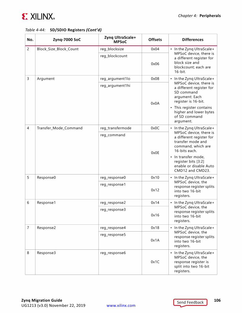
Chapter 4: Peripherals
2 Block_Size_Block_Count reg_blocksize 0x04 • In the Zynq UltraScale+ MPSoC device, there is a different register for block size and blockcount; each are 16-bit.
reg_blockcount0x06
3 Argument reg_argument1lo 0x08 • In the Zynq UltraScale+ MPSoC device, there is a different register for SD command argument: Each register is 16-bit.
• This register contains higher and lower bytes of SD command argument.
reg_argument1hi
0x0A
4 Transfer_Mode_Command reg_transfermode 0x0C • In the Zynq UltraScale+ MPSoC device, there is a different register for transfer mode and command, which are 16-bits each.
• In transfer mode, register bits [3:2] enable or disable Auto CMD12 and CMD23.
reg_command
0x0E
5 Response0 reg_response0 0x10 • In the Zynq UltraScale+ MPSoC device, the response register splits into two 16-bit registers.
reg_response10x12
6 Response1 reg_response2 0x14 • In the Zynq UltraScale+ MPSoC device, the response register splits into two 16-bit registers.
reg_response30x16
7 Response2 reg_response4 0x18 • In the Zynq UltraScale+ MPSoC device, the response register splits into two 16-bit registers.
reg_response50x1A
8 Response3 reg_response6
0x1C
• In the Zynq UltraScale+ MPSoC device, the response register is split into two 16-bit registers.
Table 4-44: SD/SDIO Registers (Cont’d)
No. Zynq-7000 SoC Zynq UltraScale+ MPSoC Offsets Differences
Zynq Migration Guide 106UG1213 (v3.0) November 22, 2019 www.xilinx.com
Send Feedback

Chapter 4: Peripherals
9 Buffer_Data_Port reg_response7 0x1E -reg_dataport 0x20 -
10 Present_state reg_presentstate
0x24
In the Zynq UltraScale+ MPSoC device, this register is 32-bits:• Bit[3] is used for
re-tuning execution request.
• Bits[28:25] are used for DAT[7:4] line.
11 Host_control_Power_control_Block_Gap_Control_Wakeup_control
reg_hostcontrol1 0x28 • In the Zynq UltraScale+ MPSoC, there are different registers for Host control, Power control, Block gap control and Wakeup control. Each register is 8-bits wide.
• In the power control, register bit[4] is used as eMMC reset.
• In the Block gap control register:° Bit [4] is used for SPI
mode enable.° Bit [5] is used to start
the Boot code access.
° Bit [6] is used to start boot code access in alternative mode.
° Bit [7] is used to check for the boot acknowledge in boot operation.
• In Host control register, bit[5] is used to control an 8-bit bus width.
reg_powercontrol 0x29reg_blockgapcontrol 0x2Areg_wakeupcontrol 0x2B
Table 4-44: SD/SDIO Registers (Cont’d)
No. Zynq-7000 SoC Zynq UltraScale+ MPSoC Offsets Differences
Zynq Migration Guide 107UG1213 (v3.0) November 22, 2019 www.xilinx.com
Send Feedback

Chapter 4: Peripherals
12 Clock_Control_Timeout_control_Software_reset
reg_clockcontrol 0x2C • In the Zynq UltraScale+ MPSoC device, there are different registers for clock control, timeout control, and software reset.
• The clock control register is 16-bits.
• Timeout control and software reset are 8-bits each.
• Clock control register bit [7:5] SD clock frequency select does the selection of the clock generator.
reg_timeoutcontrol 0x2Ereg_softwarereset
0x2F
13 Normal_interrupt_status_Error_interrupt_status
reg_normalintrsts 0x30 • In the Zynq UltraScale+ MPSoC device, there is are different registers for Normal interrupt status and Error interrupt status. Each register 16-bits.
• It supports Auto CMD23.i in normal interrupt status register.
• In card interrupt, status interrupt pins detect interrupt.° Bits [11:9] is for
interrupt pins (INT_A,INT_B and INT_C).
° Bit [12] is for re-tuning request.
° Bit [13] is for Boot acknowledge received.
° Bit [14] is for Boot operation terminated.
• In the Error interrupt status register, bit [12] is for Host Error.
reg_errorintrsts 0x32
Table 4-44: SD/SDIO Registers (Cont’d)
No. Zynq-7000 SoC Zynq UltraScale+ MPSoC Offsets Differences
Zynq Migration Guide 108UG1213 (v3.0) November 22, 2019 www.xilinx.com
Send Feedback

Chapter 4: Peripherals
14 Normal_interrupt_status_enable_Error_interrupt_status_enable
reg_normalintrstsena 0x34 • In the Zynq UltraScale+ MPSoC device, there is a different register for Normal interrupt status enable and Error interrupt status enable. Each register is 16-bits wide. It supports Auto CMD23.
• In normal interrupt status enable register:° Bits [11:9] are for
interrupt pins (INT_A,INT_B and INT_C).
° Bit [12] is for re-tuning request.
° Bit [13] is for Boot acknowledge received.
° Bit [14] is for Boot operation terminated.
• In Error interrupt status enable register, Bit [12] is for Host Error.
reg_errorintrstsena 0x36
Table 4-44: SD/SDIO Registers (Cont’d)
No. Zynq-7000 SoC Zynq UltraScale+ MPSoC Offsets Differences
Zynq Migration Guide 109UG1213 (v3.0) November 22, 2019 www.xilinx.com
Send Feedback

Chapter 4: Peripherals
15 Normal_interrupt_signal_enable_Error_interrupt_signal_enable
reg_normalintrsigena 0x38 • In the Zynq UltraScale+ MPSoC device, there are different registers for Normal interrupt signal enable and Error interrupt signal enable. Each register is of 16-bit wide, and supports Auto CMD23.
• In normal interrupt signal enable register:° Bits [11:9] are used
for interrupt pins (INT_A,INT_B and INT_C).
° Bit [12] is for re-tuning request.
° Bit 13] is for Boot acknowledge received.
° Bit [14] is used for Boot operation terminated.
• In Error interrupt signal, enable register, bit [12] is for Host Error.
reg_errorintrsigena 0x3A
16 Auto_CMD12_error_status
reg_autocmderrsts 0x3C
• In the Zynq UltraScale+ MPSoC device, this register is 16-bits.° Bit [0] and Bit [7] are
set to 0 when Auto CMD Error is generated by Auto CMD23.
Table 4-44: SD/SDIO Registers (Cont’d)
No. Zynq-7000 SoC Zynq UltraScale+ MPSoC Offsets Differences
Zynq Migration Guide 110UG1213 (v3.0) November 22, 2019 www.xilinx.com
Send Feedback

Chapter 4: Peripherals
17 Capabilities
reg_capabilities 0x40
In the Zynq UltraScale+ MPSoC device, this register is of 64-bits.• Bit[5:0] is used to show
the base clock frequency used to detect Data Timeout error.
• Bit[15:8] are for base clock frequency.
• Bit[57:30] for a description of this field see the SDIO Module Registers.
18 Maximum_current_capabilities reg_maxcurrentcap0x48
• In the Zynq UltraScale+ MPSoC device, this register is of 64-bits.
19 Force_event_for_Auto_Cmd12_Error_Status_Force_event_register_for_error_interrupt_status
reg_ForceEventforAUTOCMDErrorStatus 0x50 • In the Zynq UltraScale+
MPSoC device, there is a different register for the auto command; error status and error interrupt status. Each register is 16-bits wide.
• In Error interrupt status register bit [10] is for tuning error and there is no field for errors status such as vendor/specification, create and target response.
reg_forceeventforerrintsts 0x52
20 ADMA_error_status reg_admaerrsts0x54
• In the Zynq UltraScale+ MPSoC device, this register is 8-bits.
21 ADMA_system_address reg_admasysaddr0 0x58 • In the Zynq UltraScale+ MPSoC device, there are four ADMA system address registers of 16-bit each.
reg_admasysaddr1 0x5Areg_admasysaddr2 0x5Creg_admasysaddr3 0x5E
22 Boot_Timeout_control reg_boottimeoutcnt • Zynq-7000 SoC: 0x60
• Zynq UltraScale+ MPSoC: 0x70
-
Table 4-44: SD/SDIO Registers (Cont’d)
No. Zynq-7000 SoC Zynq UltraScale+ MPSoC Offsets Differences
Zynq Migration Guide 111UG1213 (v3.0) November 22, 2019 www.xilinx.com
Send Feedback

Chapter 4: Peripherals
SD/SDIO Host Control Registers
23 Debug_Selection - 0x64 -24 SPI_interrupt_support - 0xF0 -25 Slot_interrupt_status_Host_contro
ller_versionreg_slotintrsts 0xFC • In the Zynq UltraScale+
MPSoC device, there is a different register for the Slot interrupt status and the host controller version.
• Each register is of 16-bit wide, and it supports SD Host Specification version 3.00.
reg_hostcontrollerver 0xFE
26 - reg_hostcontrol2 0x3E -27 - reg_presetvalue0 0x60 -28 - reg_presetvalue1 0x62 -29 - reg_presetvalue2 0x64 -30 - reg_presetvalue3 0x66 -31 - reg_presetvalue4 0x68 -32 - reg_presetvalue5 0x6A -33 - reg_presetvalue6 0x6C -34 - reg_presetvalue7 0x6E -
Table 4-44: SD/SDIO Registers (Cont’d)
No. Zynq-7000 SoC Zynq UltraScale+ MPSoC Offsets Differences
No Zynq-7000 SoC RegistersZynq UltraScale+ MPSoC Devices
RegistersOffset
26 - reg_hostcontrol2 0x3E27 - reg_presetvalue0 0x6028 - reg_presetvalue1 0x6229 - reg_presetvalue2 0x6430 - reg_presetvalue3 0x6631 - reg_presetvalue4 0x6832 - reg_presetvalue5 0x6A33 - reg_presetvalue6 0x6C34 - reg_presetvalue7 0x6E
Zynq Migration Guide 112UG1213 (v3.0) November 22, 2019 www.xilinx.com
Send Feedback

Chapter 4: Peripherals
SD I/O InterfaceIn both Zynq devices, the SD interface can be routed either through MIO or EMIO pins.
SD/SDIO Bare-Metal DriversUse the Zynq UltraScale+ MPSoC device equivalent BSP. The bare-metal driver APIs for SD/SDIO of Zynq UltraScale+ MPSoC is same as that of the Zynq-7000 SoC device.
SD/SDIO Linux DriversUse the Zynq UltraScale+ MPSoC equivalent Linux driver. No change is required in the software application code. The following table shows a comparison.SD
Quad-SPI Flash ControllerThe Zynq UltraScale+ MPSoC device has both a Quad-SPI controller and a Generic Quad-SPI controller.
• The Generic Quad-SPI controller meets the requirements for generic low-level access by the software. The controller supports generic and future command sequences and future NOR/NAND flash devices.
• The Quad-SPI controller supports all features in SPI, dual-SPI, and Quad-SPI modes. The Quad-SPI controller also supports the dual parallel mode that uses two flash devices, the stacked mode that uses two flash devices.
Table 4-45: Zynq SD/SDIO Information Zynq-7000 SoC Device Zynq UltraScale+ MPSoC Device
SD0 SD1 SD0 SD1Compatible arasan,sdhci-8.9a arasan,sdhci-8.9a arasan,sdhci-8.9a arasan,sdhci-8.9aInput clocks clk_xin
clk_ahbclk_xinclk_ahb - -
Clock phandles &clkc 21&clkc 32 - - -
Interrupt parent &gic &gic - -Interrupt number 0 24 4 - - -Physical base address and size of register.
0xE01000000x1000
0xE01010000x1000
0xFF1600000x10000
0xFF1700000x10000
Zynq Migration Guide 113UG1213 (v3.0) November 22, 2019 www.xilinx.com
Send Feedback

Chapter 4: Peripherals
Quad-SPI Flash Architectural Differences
In the Zynq-7000 SoC device, the Quad-SPI controller is just a Linear Quad-SPI controller.
The Quad-SPI controller in the Zynq UltraScale+ MPSoC device is a super-set of Legacy linear Quad-SPI controller and a new Generic Quad-SPI controller.
• Register control (generic_qspi_sel) set to 1, selects the generic Quad-SPI controller. • Register control (generic_qspi_sel) set to 0, selects the legacy Quad-SPI controller. This
bit can be dynamically changed.
The DMA controller and the receive capture logic with delay line is shared between both the controllers. The following figure illustrates the top-level block diagram of the Quad-SPI controller in the Zynq UltraScale+ MPSoC device. X-Ref Target - Figure 4-16
Figure 4-16: Zynq UtlraScale+ Quad-SPI Controller Diagram
Zynq Migration Guide 114UG1213 (v3.0) November 22, 2019 www.xilinx.com
Send Feedback

Chapter 4: Peripherals
Supported Quad-SPI Operational ModesThis section lists the operational modes supported in Zynq devices.
Supported Quad-SPI Modes in Zynq-7000 SoC Device
The controller operates in one of three modes:° I/O mode
° linear addressing mode
° legacy SPI mode.
The Quad-SPI flash controller can operate in either I/O mode or linear addressing mode.
° For reads, the controller supports single, dual, and quad read modes in both I/O and linear addressing modes.
° For writes, single and quad modes are supported in I/O mode. Writes are not supported in linear addressing mode.
Supported Quad-SPI Modes in Zynq UltraScale+ MPSoC Devices
The Linear Quad-SPI controller supports the following four modes:° I/O mode
° linear mode
° legacy SPI mode
° DMA mode (with DMA_EN)
The Generic Quad-SPI controller supports two modes:° I/O mode
° DMA mode
QUAD-SPI Reset
In the Zynq-7000 SoC device, the controller has two reset domains: APB interface and the controller itself. They can be controlled together or independently. The controller can be reset using APB interface reset using the register slcr.LQSPI_RST_CTRL[LQSPI_CPU1X_RST]. It can also be reset using the PS subsystem reset through the SLCR register: slcr.LQSPI_RST_CTRL[QSPI_REF_RST].
In the Zynq UltraScale+ MPSoC device, the controller can be reset using APB interface register APB RST_LPD_IOU2[qspi_reset].
Zynq Migration Guide 115UG1213 (v3.0) November 22, 2019 www.xilinx.com
Send Feedback

Chapter 4: Peripherals
Quad SPI Clock
In both Zynq devices, the QSPI controller and I/O interface are driven by the reference clock (QSPI_REF_CLK).
The Interconnect of the controller also requires an APB interface CPU_1x clock. These clocks are generated by the PS clock subsystem.
IMPORTANT: In the Zynq UltraScale+ MPSoC device, QSPI_REF_CTRL controls the reference clock from which this register comes under APB clock control registers.
QUAD SPI Controller Configuration and Data Flow In the Zynq UltraScale+ MPSoC device, the QSPI controller consists of a Legacy linear Quad-SPI controller and a new Generic Quad-SPI controller.
Before configuring the QSPI controller, you must specify the controller type (Legacy QSPI controller or Generic QSPI controller) in the XGQSPI_SEL_OFFSET register.
The Zynq UltraScale+ MPSoC device adds a transmitter FIFO empty interrupt in the interrupt register, which specifies whether the transmitter FIFO is empty or not. In all interrupt registers, the 8th bit indicates the transmitter FIFO empty interrupt.
The Legacy QSPI and the Generic QSPI configuration flows in the Zynq devices are shown in the following diagrams. The steps that differ in Zynq UltraScale+ MPSoC devices from Zynq-7000 SoC are highlighted in red.
Zynq Migration Guide 116UG1213 (v3.0) November 22, 2019 www.xilinx.com
Send Feedback

Chapter 4: Peripherals
X-Ref Target - Figure 4-17
Figure 4-17: Legacy QSPI Controller Differences
Clock Configuration
I/O Configuration
Reset the Controller
Controller Configuration
Configure Controller Mode
Enable Controller
Transmit Data
Receive Data
Zynq Migration Guide 117UG1213 (v3.0) November 22, 2019 www.xilinx.com
Send Feedback
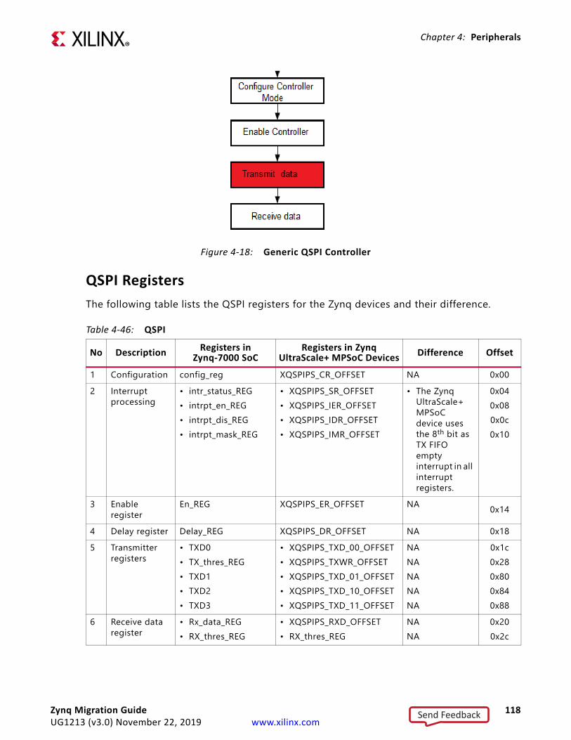
Chapter 4: Peripherals
QSPI RegistersThe following table lists the QSPI registers for the Zynq devices and their difference.
X-Ref Target - Figure 4-18
Figure 4-18: Generic QSPI Controller
Table 4-46: QSPI
No Description Registers in Zynq-7000 SoC
Registers in Zynq UltraScale+ MPSoC Devices Difference Offset
1 Configuration config_reg XQSPIPS_CR_OFFSET NA 0x002 Interrupt
processing• intr_status_REG• intrpt_en_REG• intrpt_dis_REG• intrpt_mask_REG
• XQSPIPS_SR_OFFSET• XQSPIPS_IER_OFFSET• XQSPIPS_IDR_OFFSET• XQSPIPS_IMR_OFFSET
• The Zynq UltraScale+ MPSoC device uses the 8th bit as TX FIFO empty interrupt in all interrupt registers.
0x040x080x0c0x10
3 Enable register
En_REG XQSPIPS_ER_OFFSET NA 0x14
4 Delay register Delay_REG XQSPIPS_DR_OFFSET NA 0x185 Transmitter
registers• TXD0• TX_thres_REG• TXD1• TXD2• TXD3
• XQSPIPS_TXD_00_OFFSET• XQSPIPS_TXWR_OFFSET• XQSPIPS_TXD_01_OFFSET• XQSPIPS_TXD_10_OFFSET• XQSPIPS_TXD_11_OFFSET
NANANANANA
0x1c0x280x800x840x88
6 Receive data register
• Rx_data_REG• RX_thres_REG
• XQSPIPS_RXD_OFFSET• RX_thres_REG
NANA
0x200x2c
Zynq Migration Guide 118UG1213 (v3.0) November 22, 2019 www.xilinx.com
Send Feedback

Chapter 4: Peripherals
Zynq UltraScale+ MPSoC Device-Specific Quad-SPI Registers
The following table lists the registers that are specific to Generic Quad-SPI controller in the Zynq UltraScale+ MPSoC device.
7 Slave idle count register
Slave_Idle_count_REG XQSPIPS_SICR_OFFSET • All bits in the Zynq UltraScale+ MPSoC device are reserved.
0x24
8 GPIO register GPIO GPIO N/A 0x309 Loopback
registerLPBK_DLY_ADJ LPBK_DLY_ADJ • In the Zynq
UltraScale+ MPSoC device, bits [31:6] are reserved.
0x38
10 Linear QSPI controller register
LQSPI_CFG XQSPIPS_LQSPI_CR_OFFSET • In Zynq UltraScale+ MPSoC Devices bits 10:8 are reserved and more read instruction codes are added.
• Bit 27 is used for AXI address appending.
0xA0
LQSPI_STS XQSPIPS_LQSPI_SR_OFFSET • In Zynq UltraScale+ MPSoC device, the register width is 32-bits.
• More functionality is added.
0xA4
11 Module Identification register
MOD_ID MOD_ID N/A0xFC
Table 4-46: QSPI (Cont’d)
No Description Registers in Zynq-7000 SoC
Registers in Zynq UltraScale+ MPSoC Devices Difference Offset
Zynq Migration Guide 119UG1213 (v3.0) November 22, 2019 www.xilinx.com
Send Feedback

Chapter 4: Peripherals
Table 4-47: Zynq UltraScale+ MPSoC Device-Specific RegistersNo Description Registers Offset1 Transfer size register TRANSFER_SIZE 0xC42 Dummy cycle enable register DUMMY_CYCLE_EN 0xC83 Generic QSPI configuration register XGQSPIPS_CR_OFFSET 0x1004 Generic QSPI interrupt registers XGQSPIPS_ISR_OFFSET
XGQSPIPS_IER_OFFSETXGQSPIPS_IDR_OFFSETXGQSPIPS_IMR_OFFSET
0x1040x1080x10C0x110
5 Generic QSPI Enable registers XGQSPIPS_EN_OFFSET 0x1146 Transmitter registers XGQSPIPS_TX_FIFO_OFFSET
XGQSPIPS_TX_THRESH_OFFSET0x11C0x128
7 Receiver registers XGQSPIPS_RX_FIFO_OFFSETXGQSPIPS_RX_THRESH_OFFSETXGQSPIPS_RX_COPY_OFFSETXGQSPIPS_ECO_OFFSET
0x1200x12C0x1640x1F8
8 Generic QSPI write protect register XGQSPIPS_GPIO_THRESH_OFFSET 0x1309 Generic QSPI Loopback clock delay
adjustment registerXGQSPIPS_LPBK_DLY_ADJ_OFFSET 0x138
10 Generic QSPI FIFO register XGQSPIPS_GEN_FIFO_OFFSETXGQSPIPS_FIFO_CTRL_OFFSETXGQSPIPS_GENFIFO_THRSH_OFFSETXGQSPIPS_GENFIFO_STS_OFFSETXGQSPIPS_GENFIFO_SNAPSHOT_OFFSET
0x1400x14C0x1500x15C0x160
11 Generic QSPI select register XGQSPIPS_SEL_OFFSET 0x14412 Poll configuration registers XGQSPIPS_POLL_OFFSET
XGQSPIPS_POLL_TIMEOUT_OFFSET0x1540x158
13 Generic QSPI Module identification register
XGQSPIPS_MOD_ID_OFFSET 0x1FC
14 DMA registers QSPIDMA_DST_ADDRQSPIDMA_DST_SIZEQSPIDMA_DST_STSQSPIDMA_DST_CTRLQSPIDMA_DST_I_STSQSPIDMA_DST_I_ENQSPIDMA_DST_I_DISQSPIDMA_DST_I_MASKQSPIDMA_DST_CTRL2QSPIDMA_DST_ADDR_MSB
0x8000x8040x8080x80C0x8140x8180x81C0x8200x8240x828
15 Future Potential ECO register QSPIDMA_FUTURE_ECO 0xFFC
Zynq Migration Guide 120UG1213 (v3.0) November 22, 2019 www.xilinx.com
Send Feedback

Chapter 4: Peripherals
QSPI I/O InterfaceIn both Zynq devices QSPI I/O signals are available through the MIO pins only.
QSPI Bare-Metal DriversThe following table specifies the bare-metal API differences in Zynq device for QSPI.
Table 4-48: QSPI Bare-Metal Driver DifferencesZynq-7000 SoC API Zynq UltraScale+ MPSoC API Difference
XQspiPs_CfgInitialize XQspiPsu_CfgInitialize Steps that are different in Zynq UltraScale+ MPSoC Devices API:• Variable initializations.• Mask to set desired SPI mode.• Waiting for component to be
ready.XQspiPs_Reset XQspiPsu_Reset Zynq UltraScale+ MPSoC device
API includes: • Setting the default value for
each fields.• DMA Initialization.• Setting the threshold registers
with the reset values.• Resetting the Loopback delay
registerXQspiPs_Abort XQspiPsu_Abort Aborting the transfer in the
Zynq-7000 SoC:• De-assert slave select lines.• QSPI Software Reset.• Set the RX and TX FIFO
threshold to reset value.In the Zynq UltraScale+ MPSoC device:• Clear and disable interrupts.• Clear FIFO.• Switch to I/O mode to Clear RX
FIFO.
Zynq Migration Guide 121UG1213 (v3.0) November 22, 2019 www.xilinx.com
Send Feedback

Chapter 4: Peripherals
XQspiPs_PolledTransfer XQspiPsu_PolledTransfer In Zynq-7000 SoC: • Check whether there is another
transfer in progress.• Set the busy flag.• Set up buffer pointers.• Set the RX FIFO threshold.• Set the slave select.• Enable the device.• Check for WRSR instruction if
not present,assign current instruction, size and TXD register to be used.
• Get the complete command.• Write the command to the FIFO.• Start the transfer.• Finish by polling TX FIFO status. • Clear the busy flag.• Disable the device.• Reset the RX FIFO threshold to
one.In Zynq UltraScale+ MPSoC: • Check whether there is another
transfer in progress.• Check for ByteCount upper limit
- 2^28 for DMA.• Set the busy flag.• Enable the device.• Select slave.• Write the GENFIFO entries to
transmit the messages requested.
• Transmit data.• Receive data.• De-select slave.• Clear the busy flag.• Disable the device.
- XQspiPsu_InterruptTransfer -
Table 4-48: QSPI Bare-Metal Driver Differences (Cont’d)
Zynq-7000 SoC API Zynq UltraScale+ MPSoC API Difference
Zynq Migration Guide 122UG1213 (v3.0) November 22, 2019 www.xilinx.com
Send Feedback

Chapter 4: Peripherals
XQspiPs_InterruptHandler XQspiPsu_InterruptHandler In the Zynq-7000 SoC device:• Clear the interrupts• Process the interrupts and take
action accordingly.• Disable the interrupt.• If the Slave select is being
manually controlled, disable it because the transfer is complete.
• Clear the busy flag.• Disable the device.• Reset the RX FIFO threshold to
one.In the Zynq UltraScale+ MPSoC device: • Cleared on read.• If DMA mode clear the DMA
interrupt.• Process the interrupt.• Disable the interrupt.• Clear the busy flag.• Disable the device.• Call status handler to indicate
completion.XQspiPs_SetStatusHandler XQspiPsu_SetStatusHandler No Change.
- XQspiPsu_SelectSpiMode -- XQspiPsu_TXRXSetup -- XQspiPsu_FillTxFifo -- XQspiPsu_SetupRxDma -- XQspiPsu_GenFifoEntryCSAssert -- XQspiPsu_GenFifoEntryData -- XQspiPsu_GenFifoEntryCSDeAssert -- XQspiPsu_ReadRxFifo -
XQspiPs_GetReadData - -XQspiPs_SetSlaveSelect - -XQspiPs_Transfer - -XQspiPs_LqspiRead - -XQspiPs_ConfigTable XQspiPsu_ConfigTable • The Zynq UltraScale+ MPSoC
device has bus width information.
Table 4-48: QSPI Bare-Metal Driver Differences (Cont’d)
Zynq-7000 SoC API Zynq UltraScale+ MPSoC API Difference
Zynq Migration Guide 123UG1213 (v3.0) November 22, 2019 www.xilinx.com
Send Feedback

Chapter 4: Peripherals
QSPI Linux Drivers
The following lists the flow of a linux driver in both the Zynq devices.
Initialize Hardware
1. Select the GQSPI mode.2. Clear and disable interrupts.3. Clear the DMA status.4. Disable the GQSPI.5. Manual start.6. Little endian by default.7. Disable poll time out.8. Set hold bit.9. Clear pre-scalar by default.10. Clear the TX and RX FIFO.11. Set by default to allow for high frequencies.
XQspiPs_ResetHw - -XQspiPs_LinearInit - -XQspiPs_SetOptions XQspiPsu_SetOptions • In the Zynq-7000 SoC device,
LQSPI configuration is done.• In the Zynq UltraScale+ MPSoC
device, manual start variable is set based on condition.
- XQspiPsu_ClearOptions -XQspiPs_GetOptions XQspiPsu_GetOptions • In Zynq-7000 SoC LQSPI options
are checked.XQspiPs_SetClkPrescaler XQspiPsu_SetClkPrescaler No Change
- XQspiPsu_SelectFlash -- XQspiPsu_SetReadMode -
XQspiPs_GetClkPrescaler - -XQspiPs_SetDelays - -XQspiPs_GetDelays - -XQspiPs_LookupConfig XQspiPsu_LookupConfig No ChangeXQspiPs_SelfTest - -
Table 4-48: QSPI Bare-Metal Driver Differences (Cont’d)
Zynq-7000 SoC API Zynq UltraScale+ MPSoC API Difference
Zynq Migration Guide 124UG1213 (v3.0) November 22, 2019 www.xilinx.com
Send Feedback

Chapter 4: Peripherals
12. Reset thresholds.13. Initialize DMA.14. Enable the GQSPI.
Prepare Transfer HardwareThis is the same in both the Zynq devices.
Chip Select
1. Choose slave select line.2. Select the bus.3. Dummy generic FIFO entry. Manually start the generic FIFO command.4. Wait until the generic FIFO command is empty.
Start transferSet up the transfer.
Transmitter Receiver Setup
1. Select spi mode.2. Fill transmitter FIFO, or setup the receiver DMA.
Interrupt TransferIn the Zynq UltraScale+ MPSoC device, the DMA interrupts are also processed. SuspendSame as Zynq-7000 SoC device.ResumeSame as Zynq-7000 SoC device.
Zynq Migration Guide 125UG1213 (v3.0) November 22, 2019 www.xilinx.com
Send Feedback

Chapter 4: Peripherals
Device Tree Binding
The following table shows the device tree binding for Zynq devices.
Static Memory Controller
Static Memory Controller Architectural DifferencesIn the Zynq-7000 SoC device, the static memory controller (SMC) can be used either as a NAND flash controller or a parallel port memory controller. SMC supports the following:
° NAND Flash
° Asynchronous SRAM
° NOR Flash.
The operational registers of the SMC are configured through an APB interface.
The NAND interface in the Zynq-7000 SoC device supports the following:
° 1-bit ECC
° Open NAND flash interface working group (ONFI) Specification 1.0
° Up to a 1 GB device
° 8 16-bit I/O width with a single chip select
In the Zynq UltraScale+ MPSoC device, there is dedicated NAND flash memory controller. The NAND flash controller has an AXI interface, which allows the Arm® processor to configure the operational registers sitting inside the NAND flash controller.
Table 4-49: Device Tree Binding
Information Zynq-7000 SoC Zynq UltraScale+ MPSoC Devices
Compatible xlnx,zynq-qspi-1.0 xlnx,zynqmp-qspi-1.0Input clock ref_clk pclk ref_clk pclkClock phandle &clkc 10 &clkc 43 &misc_clk &misc_clkInterrupt number 0 19 4 0 15 4Interrupt parent &intc &gicNumber of Chip select 1 1Physical base address and size of register
0xe000d000 0x1000 0x0 0xff0f0000 0x1000 0x0 0xc0000000 0x8000000
Zynq Migration Guide 126UG1213 (v3.0) November 22, 2019 www.xilinx.com
Send Feedback

Chapter 4: Peripherals
The following diagram shows the block diagram of the NAND memory controller in the Zynq-7000 SoC device. The operational registers of the SMC are configured through an APB interface.
The NAND interface supports the following: ° 1-bit ECC
° Open NAND flash interface working group (ONFI) standards 1.0, 2.0, 2.1, 2.2, 2.3, 3.0, and 3.1
° A maximum of 512 Gb of NAND flash memory
° An 8-bit interface to the flash memories
In the Zynq UltraScale+ MPSoC device, there is a dedicated NAND flash memory controller. The NAND flash controller has an advanced eXtensible interface (AXI) interface, which allows the Arm® processor to configure the operational registers sitting inside the NAND flash controller.
SMC Clock
The static memory controller (SMC) in the Zynq-7000 SoC device has two clock domains that the CPU_1x and SMC_Ref clocks drive. The clock generator controls these clocks. The two clock domains are asynchronous to each other.
In the Zynq UltraScale+ MPSoC device, the NAND controller also has two clock domains that are driven by the CPU_1x and the reference clocks. The NAND_REF_CTRL register controls the reference clock. This control register comes under APB clock control registers.
X-Ref Target - Figure 4-19
Figure 4-19: Zynq UltraScale+ MPSoC Device NAND Static Flash Memory Controller
Zynq Migration Guide 127UG1213 (v3.0) November 22, 2019 www.xilinx.com
Send Feedback

Chapter 4: Peripherals
SMC Reset
In the Zynq-7000 SoC device, the SMC controller has two reset inputs that the reset subsystem controls. The AXI and APB interfaces use the SMC CPU_1x reset. The SMC_Ref reset is for the FIFOs, and the rest of the controller including the control and status registers.
In the Zynq UltraScale+ MPSoC device, the RST_LPD_IOU2 register resets the SMC controller. The RST_LPD_IOU2 is a part of APB control registers (CRL_APB).
SMC supports BCH error correction code (ECC) data widths of 4=, 8-, 12-, and 24-bits.
The NAND Flash interface supports the open NAND flash interface working group (ONFI) standards 1.0, 2.0, 2.1, 2.2, 2.3, 3.0, and 3.1. The interface supports a maximum of 512 Gb of NAND flash memory. It provides an 8-bit interface to the flash memories
SMC Clock
In the Zynq-7000 SoC, SMC has two clock domains that are driven by the CPU_1x and SMC_Ref clocks. These clocks are controlled by the clock generator. The two clock domains are asynchronous to each other.
In Zynq UltraScale+ MPSoC devices, NAND controller also has two clock domain that are driven by the CPU_1x and reference clock. The reference clock is controlled by NAND_REF_CTRL register. These control register comes under APB clock control registers.
SMC Configuration and Data Flow
See this link to the “Trust Zone” section in the Zynq-7000 SoC Technical Reference Manual (UG585) [Ref 6].
See this link to the “SMC Configuration” chapter in the Zynq UltraScale+ MPSoC Technical Reference Manual (UG1085) [Ref 10].
SMC NAND Registers
The following table specifies the NAND memory controller register set in Zynq UltraScale+ MPSoC device. The register set in Zynq UltraScale+ MPSoC device is different than in Zynq-7000 SoC device.
Zynq Migration Guide 128UG1213 (v3.0) November 22, 2019 www.xilinx.com
Send Feedback

Chapter 4: Peripherals
Table 4-50: Zynq UltraScale+ MPSoC Device Registers
No Type Zynq UltraScale+ MPSoC Device Registers Description Offset
1 Packet control register
Packet_Register Packet register allows control of packet count and size. 0x00
2 Memory bank register
Memory_Address_Register1 32-bit argument points to the flash memory area. 0x04
Memory_Address_Register2 Memory address register 2. 0x083 NAND
command register
Command_Register Command register to configure DMA transfer and page size. 0x0C
4 NAND program register
Program_Register Program register. 0x10
5 Interrupt register
Interrupt_Status_Enable_RegisterInterrupt_Signal_Enable_RegisterInterrupt_Status_Register
Interrupt status enable register.Interrupt signal enable register.Interrupt status register.
0x140x180x1C
6 Status register Ready_BusyFlash_Status_Register
Ready busy registerFlash status.
0x200x28
7 System address register
DMA_system_address1_register DMA system address register. 0x24
8 NAND timing information register
Timing_Register Sets timing for the NVDDR mode. 0x2C
9 Data port register
Buffer_Data_Port_Register NAND flash internal buffer access register. 0x30
10 ECC register ECC_RegisterECC_Error_Count_RegisterECC_Spare_Command_Register
0x340x380x3C
11 Error status register
Error_count_1bit_registerError_count_2bit_registerError_count_3bit_registerError_count_4bit_registerError_count_5bit_registerError_count_6bit_registerError_count_7bit_registerError_count_8bit_register
Error count 1-bit register.Error count 2-bit register.Error count 3-bit register.Error count 4-bit register.Error count 5-bit register.Error count 6-bit register.Error count 7-bit register.Error count 8-bit register.
0x400x440x480x4C0x5C0x600x640x68
12 System address register
DMA_system_address0_register DMA system address register. 0x50
13 DMA register DMA_buffer_boundary_register DMA buffer boundary register. 0x54
Zynq Migration Guide 129UG1213 (v3.0) November 22, 2019 www.xilinx.com
Send Feedback

Chapter 4: Peripherals
NAND SMC I/O Interface
In both Zynq devices, the controller signal are routed to MIO.
IMPORTANT: NAND is not supported in the EMIO.
NAND Bare-Metal Drivers
The following table specifies all the APIs in the NAND driver of both Zynq devices, and their differences.
14 CPU release register
CPU_Release_Register CPU release register 0x58
15 NAND data interface register
Data_interface_register Sets SDR mode and NV-DDR mode. 0x6C
Table 4-50: Zynq UltraScale+ MPSoC Device Registers
No Type Zynq UltraScale+ MPSoC Device Registers Description Offset
Table 4-51: NAND Bare-Metal DriversZynq-7000 SoC Zynq UltraScale+ MPSoC Devices Differences
XNandPs_CfgInitialize XNandPsu_CfgInitialize In the Zynq UltraScale+ MPSoC devices: • Initialize InstancePtr
configuration structure.• Operate in Polling Mode.• Enable MDMA mode by
default.• Initialize the NAND flash
targets.• Set ECC mode.• Initialize ECC Error flip
counters.• Scan for the bad block table
(bbt) stored in the flash & load it in memory (RAM). ° If bbt is not found, create
bbt by scanning factory marked bad blocks and store it in last good blocks of flash.
XNandPs_EccSetCfg - -XNandPs_EccSetMemCmd1 - -XNandPs_EccSetMemCmd2 - -
Zynq Migration Guide 130UG1213 (v3.0) November 22, 2019 www.xilinx.com
Send Feedback

Chapter 4: Peripherals
XNandPs_EccDisable - -XNandPs_EccHwInit - -XNandPs_EccSwInit - -XNandPs_Read XNandPsu_Read The Zynq UltraScale+ MPSoC
device: • Checks and skips bad blocks.• Copies into Destination
buffer.XNandPs_ReadCache - -XNandPs_Write XNandPsu_Write The Zynq UltraScale+ MPSoC
device: • Checks and skips bad blocks.• Writes into the source buffer.
XNandPs_WriteCache - -XNandPs_SendCommand - -XNandPs_ReadSpareBytes XNandPsu_ReadSpareBytes The Zynq UltraScale+ MPSoC
device: • Checks for DMA mode and
enable the interrupt.• Program the command, page
size, column, page and block address.
• Program for chip select.• Set Read command in
Program Register• Read Spare Data.
XNandPs_WriteSpareBytes XNandPsu_WriteSpareBytes The Zynq UltraScale+ MPSoC device: • Checks for ECC mode.• Calculates ECC free positions
before and after ECC code.• Program Command hack for
change write column.• Program Page Size, Packet
Size, Packet Count, Column, Page and Block address.
• Set Page Program in Program Register.
• Write Spare Data.XNandPs_IsBusy - -XNandPs_EccCalculate - -
Table 4-51: NAND Bare-Metal Drivers (Cont’d)
Zynq-7000 SoC Zynq UltraScale+ MPSoC Devices Differences
Zynq Migration Guide 131UG1213 (v3.0) November 22, 2019 www.xilinx.com
Send Feedback

Chapter 4: Peripherals
XNandPs_EccCorrect - -XNandPs_ReadPage_HwEcc - -XNandPs_ReadPage XNandPsu_ReadPage • In the Zynq UltraScale+
MPSoC device, the hardware ECC block is used for checking ECC Error.
XNandPs_WritePage_HwEcc - -XNandPs_WritePage - -XNandPs_EraseBlock XNandPsu_EraseBlock In the Zynq UltraScale+ MPSoC
device: • It Enables Transfer Complete
Interrupt.• Program
Command,column,page and block address.
• Program for chip select.• Set Block Erase in Program
Register.• Poll for Transfer Complete
event.XNandPs_ReadBuf - -XNandPs_WriteBuf - -
- XNandPsu_FlashInit -- XNandPsu_InitGeometry -- XNandPsu_InitFeatures -- XNandPsu_CheckOnDie -- XNandPsu_EnableDmaMode -- XNandPsu_DisableDmaMode -- XNandPsu_EnableEccMode -- XNandPsu_DisableEccMode -- XNandPsu_PollRegTimeout -- XNandPsu_SetPktSzCnt -- XNandPsu_SetPageColAddr -- XNandPsu_SetPageSize -- XNandPsu_SetEccAddrSize -- XNandPsu_SetEccSpareCmd -- XNandPsu_SelectChip -- XNandPsu_OnfiReset -
Table 4-51: NAND Bare-Metal Drivers (Cont’d)
Zynq-7000 SoC Zynq UltraScale+ MPSoC Devices Differences
Zynq Migration Guide 132UG1213 (v3.0) November 22, 2019 www.xilinx.com
Send Feedback

Chapter 4: Peripherals
- XNandPsu_OnfiReadStatus -- XNandPsu_OnfiReadId -- XNandPsu_OnfiReadParamPage -- XNandPsu_CalculateLength -- XNandPsu_Erase -- XNandPsu_ProgramPage -- XNandPsu_GetFeature -- XNandPsu_SetFeature -- XNandPsu_ChangeTimingMode -- XNandPsu_ChangeReadColumn -- XNandPsu_ChangeWriteColumn -- XNandPsu_InitExtEcc -- XNandPsu_Prepare_Cmd -- XNandPsu_Data_ReadWrite -- XNandPsu_Fifo_Write -- XNandPsu_Fifo_Read -- XNandPsu_Update_DmaAddr -- XNandPsu_Device_Ready -- XNandPsu_WaitFor_Transfer_Complete -
XNandPs_InitBbtDesc XNandPsu_InitBbtDesc • In the Zynq UltraScale+ MPSoC device, it also sets the Maximum Block.
XNandPs_CreateBbt XNandPsu_CreateBbt -XNandPs_ScanBbt XNandPsu_ScanBbt -XNandPs_ConvertBbt XNandPsu_ConvertBbt -XNandPs_ReadBbt XNandPsu_ReadBbt -XNandPs_SearchBbt XNandPsu_SearchBbt -XNandPs_WriteBbt XNandPsu_WriteBbt -XNandPs_UpdateBbt XNandPsu_UpdateBbt -XNandPs_MarkBbt XNandPsu_MarkBbt -XNandPs_IsBlockBad XNandPsu_IsBlockBad -XNandPs_MarkBlockBad XNandPsu_MarkBlockBad -XNandPs_ConfigTable XNandPsu_ConfigTable • In the Zynq UltraScale+
MPSoC device, the table has only Base Address.
Onfi_ReadData - -
Table 4-51: NAND Bare-Metal Drivers (Cont’d)
Zynq-7000 SoC Zynq UltraScale+ MPSoC Devices Differences
Zynq Migration Guide 133UG1213 (v3.0) November 22, 2019 www.xilinx.com
Send Feedback

Chapter 4: Peripherals
NAND Linux Drivers
The following steps provide the sequence of operation in the Zynq UltraScale+ MPSoC device NAND controller Linux driver:
1. Reset the NAND contr.oller.2. NAND Initialization:
a. Allocate memory for NAND FIFO.b. Set the address of NAND I/O lines.c. Set the driver entry points.d. Scan to find the device and get the page size.e. Send the command for reading the device ID.f. Read manufacturer and device IDs.g. If ECC is enabled, set the ECC parameters.h. Initialize the ECC.i. Perform the NAND operations according to the commands, that could be:
- Read Command- Write Command- Erase command- Read Status command
Onfi_WriteData - -Onfi_CmdReadStatus - -Onfi_CmdReset - -Onfi_CmdReadId - -Onfi_CmdReadParamPage - -Onfi_GetFeature - -Onfi_SetFeature - -Onfi_Crc16 - -Onfi_ReadParamPage - -Onfi_NandInit - -
- XNandPsu_OnfiParamPageCrc -XNandPs_LookupConfig XNandPsu_LookupConfig -
Table 4-51: NAND Bare-Metal Drivers (Cont’d)
Zynq-7000 SoC Zynq UltraScale+ MPSoC Devices Differences
Zynq Migration Guide 134UG1213 (v3.0) November 22, 2019 www.xilinx.com
Send Feedback

Chapter 4: Peripherals
DDR Memory ControllerIn Zynq UltraScale+ MPSoC Devices, DDR controller supports DDR3, DDR3L, LPDDR3, DDR4, and LPDDR4. It does not support DDR2 and LPDDR2 that was supported in Zynq-7000 SoC device DDR controller.
DDR Architectural DifferencesThe following table summarizes the difference between Zynq Device DDR controller.Table 4-52: Zynq Device DDR Controller
Features Zynq-7000 SoC Zynq UltraScale+ MPSoC Devices
DDR Controller Subsystem Blocks
Consists of three major blocks: • AXI memory port interface
(DDRI).• A core controller with
transaction scheduler (DDRC). • A controller with digital PHY
(DDRP).
Consists of six major blocks: • Xilinx Memory Protection Unit
(XMPU)• QoS controller• DDR controller• DDR PHY• AXI-to-APB bridge• AXI performance monitor
Interfaces • Has four 64-bit synchronous AXI interfaces
Has six AXI interfaces: • One is Connected to the RPU
and two to the CCI-400 • The others are multiplexed
across the DisplayPort controller, FPD-DMA, and the PL.
• Of the six interfaces, five are 128-bits wide and the sixth interface (tied to the RPU) is 64-bits wide.
DDR System Controller • Does not support UDIMMs and RDIMMs.
• Supports UDIMMs and RDIMMs.
Error Correction Code (ECC) • Optional ECC in 16-bit data width configuration.
• ECC support in 32-bit and 64-bit mode, 2-bit error detection, and 1-bit error correction
QoS Support No Yes. • Three traffic classes on read
commands• Two traffic classes on write
commands
Zynq Migration Guide 135UG1213 (v3.0) November 22, 2019 www.xilinx.com
Send Feedback

Chapter 4: Peripherals
DDR Supported Modes
In the Zynq-7000 SoC device, the DDR controller supports the following power saving modes:
° Changing clock frequency
° Power down
° Deep power down
° Self-refresh
° Clock
° Pre-charge power downThe Zynq UltraScale+ MPSoC device DDR controller supports Maximum Power Saving Mode along with the previously mentioned power modes where the user can control the entry and exit of the DDR controller pre-charge power down mode.For more information about the configuration of the DDR controller in these power saving modes, see this link to the DDR Memory Controller Programming Model section of the “DDR Memory Controller” chapter in Zynq UltraScale+ MPSoC Technical Reference Manual (UG1085) [Ref 10].
DDR Configuration and Data Flow
In Zynq devices, DDR initialization involves the following phases:
• PHY initialization• DRAM initialization• Data training
The DDR PHY has an embedded state machines that performs DRAM initialization based on the DRAM type programmed into the PHY registers. To trigger DRAM initialization using the PHY, the PIR = x0000_0081 or PIR = x0010_0081 when RDIMM is required. Alternatively, the DDR controller can perform DRAM initialization.
Content Addressable Memories (CAM)
• Contains two 32-entry content addressable memories to perform DDR data service scheduling to maximize DDR memory efficiency.
• Read and write buffers in fully associative content addressable memories; configurable in powers of two, up to 64 reads and 64 writes.
DDR PHY Loopback mode Support
No Yes
Table 4-52: Zynq Device DDR Controller (Cont’d)
Features Zynq-7000 SoC Zynq UltraScale+ MPSoC Devices
Zynq Migration Guide 136UG1213 (v3.0) November 22, 2019 www.xilinx.com
Send Feedback

Chapter 4: Peripherals
For more information on configuration of DDR PHY and Data training, see this link to the DDR Initialization section in the “DDR Memory Controller” chapter in the Zynq UltraScale+ MPSoC Technical Reference Manual (UG1085) [Ref 10].
DDR Registers
See the register database for DDRC, DDR_PHY, DDR_QoS_CTRL, and XMPU_DDR modules at the following link: Zynq UltraScale Registers [Ref 15].
DDR Bare-Metal Drivers
Use the Zynq UltraScale+ MPSoC device-equivalent BSP. The bare-metal driver APIs for DDRC of the Zynq UltraScale+ MPSoC device is the same as that of the Zynq-7000 SoC device.
DMA ControllerTo accelerate the data transfers to and from system memories and PL peripherals, Zynq devices include a DMA controller.
In Zynq-7000 SoC devices, there is one DMA controller.
In Zynq UltraScale+ MPSoC devices, there are two general purpose DMA controllers:
° One instance is located in the full-power domain (FPD).
° Another is located in the low-power domain (LPD).
The DMA instance located in the FPD is referred as the full-power DMA (FPD-DMA) and instance located in LPD is referred as the low-power DMA (LPD-DMA).
DMA controller is designed to support memory-to-memory and memory-to-I/O buffer transfers. The controller can be configured with up to eight DMA channels. Each channel corresponds to a thread running on the DMA engine’s processor.
Zynq Migration Guide 137UG1213 (v3.0) November 22, 2019 www.xilinx.com
Send Feedback

Chapter 4: Peripherals
DMA Architectural DifferencesThe following table summarizes the architectural differences between the Zynq-7000 SoC device and the Zynq UltraScale+ MPSoC device DMA controller.
DMA Configuration and Data Flow Configuration of DMA controller and its data flow in Zynq UltraScale+ MPSoC devices is explained in detail at this link to the “DMA Controller” chapter in the Zynq UltraScale+ MPSoC Technical Reference Manual (UG1085) [Ref 10].
DMA RegistersRegister database for DMA Controller of Zynq UltraScale+ MPSoC Devices can be found at in the “ZDMA Registers” in Zynq UltraScale+ MPSoC Register Reference (UG1087) [Ref 15].
DMA Linux DriversThe implementation of Linux driver APIs in Zynq UltraScale+ MPSoC devices for DMA controller differs completely from the Zynq-7000 SoC device.
The following steps specify the sequence of operations in the Linux driver for Zynq UltraScale+ MPSoC devices for the DMA controller.
1. Reset the DMA channel.2. Initialize the DMA channel with the following steps:
a. Enable/disable over-fetch.b. Enable/disable rate control.
Table 4-53: DMA Controller DifferencesZynq-7000 SoC DMA Controller Zynq UltraScale+ MPSoC DMA Controller
Supports AXI-3. Supports AXI-4 and backward compatible with AXI-3.
AXI bus width is 64-bit. AXI bus width is: 128-bit in FPD-DMA and 64-bit in LPD-DMA.
Has an instruction execution engine. The program code for the DMA engine is written by the software into the memory region that is accessed by the controller. The instruction set includes instructions for DMA transfers and management.
There is no separate instruction engine. The software directly programs the DMA registers to enable and manage DMA transfers.
Changes to the priority of a DMA channel over any other DMA channels are not supported.
Changes to the priority of a DMA channel over any other DMA channels are supported.
DMA does not have over fetch feature. DMA has over fetch feature.Does not support DMA PAUSE. Support for DMA START, STOP, and PAUSE.
Zynq Migration Guide 138UG1213 (v3.0) November 22, 2019 www.xilinx.com
Send Feedback

Chapter 4: Peripherals
c. Set the transfer type.d. Clear all the interrupt account registers.e. Set the AXI and QoS attributes.
3. Allocate channel resources4. Prepare the transfer descriptors for simple/scatter-gather DMA transfer.5. If DMA Interrupt is enabled, prepare the interrupt handlers.6. Start the DMA transfer.7. Check the transfer status.8. Free the channel resources.
DMA Device Tree BindingThe following is an example device tree binding for FPD-DMA:
fpd_dma_chan1: dma@FD500000 {compatible = “xlnx,zynqmp-dma-1.0”;reg = <0x0 0xFD500000 0x1000>;interrupt-parent = <&gic>;interrupts = <0 117 4>;xlnx,bus-width = <128>;xlnx,include-sg;xlnx,overfetch;xlnx,ratectrl = <0>;xlnx,src-issue = <16>;xlnx,desc-axi-cohrnt;xlnx,src-axi-cohrnt;xlnx,dst-axi-cohrnt;xlnx,desc-axi-qos = <0>;xlnx,desc-axi-cache = <0>;xlnx,src-axi-qos = <0>;xlnx,src-axi-cache = <2>;xlnx,dst-axi-qos = <0>;xlnx,dst-axi-cache = <2>;xlnx,src-burst-len = <4>;xlnx,dst-burst-len = <4>;
};
Zynq Migration Guide 139UG1213 (v3.0) November 22, 2019 www.xilinx.com
Send Feedback

Chapter 4: Peripherals
TimersIn the Zynq-7000 SoC device, each Cortex-A9 processor has its own private 32-bit timer and 32-bit watchdog timer. Both processors share a global 64-bit timer. These timers are always clocked at 1/2 of the CPU frequency (CPU_3x2x).
On the system level, there is a 24-bit watchdog timer and there are two 16-bit triple timer/counters.
The system watchdog timer is clocked at 1/4 or 1/6 of the CPU frequency (CPU_1x), or can be clocked by an external signal from an MIO pin or from the PL. The two triple timers/counters are always clocked at 1/4 or 1/6 of the CPU frequency (CPU_1x), and are used to count the widths of signal pulses from an MIO pin or from the PL.
The Zynq UltraScale+ MPSoC device has two system watchdog timers (SWDT), one each for the RPU and APU subsystem. The RPU SWDT is in the low-power domain (LPD), and the APU SWDT is in the full-power domain (FPD). Each of these SWDT provide error condition information to the error manager. The APU SWDT can be used to reset the APU or the FPD. The RPU SWDT can be used to reset the RPU or the processing system (PS).
In full-power domain mode, the APU software uses Cortex®-A53 MPCore generic timers. However, when the full-power domain power is off, then the generic timers cannot be used (as wake events for the APU cores).
A pair of triple-timer counters (TTCs) is provided for the APU. These TTCs are implemented in the low-power domain. When the full-power domain power is off, the TTCs can be set up as wake events for the APU cores. The RPU has its dedicated system watchdog timer and a dual triple-timer counter that reside in the low-power domain. This allows isolation between the RPU and APU without the need for sharing watchdog functions. The Cortex-A53 MPCore provides integrated generic timers that require an external counter (system counter).
Table 4-54: Timer DifferencesZynq-7000 SoC Timers Zynq UltraScale+ MPSoC Timers
CPU0 CPU1 APU RPU32-bit Timer 32-bit Timer System Watchdog
Timers (SWDT)System Watchdog Timers (SWDT)
32-bit Watchdog Timer 32-bit Watchdog Timer Two 32-bit Triple-Timer Counters
Two 32-bit Triple-Timer Counter
Global 64-bit Timer(Shared by both the core) Generic Timers -System level Timers:24-bit Watchdog Timer(SWDT).Two 16-bit Triple Timer/Counters.
-
Zynq Migration Guide 140UG1213 (v3.0) November 22, 2019 www.xilinx.com
Send Feedback

Chapter 4: Peripherals
Timer Registers
The following table lists all the timer registers in both Zynq devices.
Table 4-55: Timer Differences
No Type Zynq-7000 SoC Registers Zynq UltraScale+ MPSoC Registers and Diff (1,2,3) Offset
1 SWDT MODE MODE (1) 0x00CONTROL CONTROL 0x04RESTART RESTART 0x08STATUS STATUS 0x0CMatch_2_Counter_2 Match_2_Counter_2 (2) 0x40Match_2_Counter_3 Match_2_Counter_3(2) 0x44Match_3_Counter_1 Match_3_Counter_1(2) 0x48Match_3_Counter_2 Match_3_Counter_2(2) 0x4CMatch_3_Counter_3 Match_3_Counter_3(2) 0x50Interrupt_Register_1 Interrupt_Register_1 0x54Interrupt_Register_2 Interrupt_Register_2 0x58Interrupt_Register_3 Interrupt_Register_3 0x5CInterrupt_Enable_1 Interrupt_Enable_1 0x60Interrupt_Enable_2 Interrupt_Enable_2 0x64Interrupt_Enable_3 Interrupt_Enable_3 0x68Event_Control_Timer_1 Event_Control_Timer_1 (3) 0x6CEvent_Control_Timer_2 Event_Control_Timer_2 (3) 0x70Event_Control_Timer_3 Event_Control_Timer_3 (3) 0x74
Notes: 1. In Zynq UltraScale+ MPSoC, bits[6:4] are used for reset length.2. In Zynq UltraScale+ MPSoC, it is 32-bit wide.3. In Zynq UltraScale+ MPSoC, it is 4-bit wide. Bit[4] is used for Test mode.
Zynq Migration Guide 141UG1213 (v3.0) November 22, 2019 www.xilinx.com
Send Feedback

Chapter 4: Peripherals
Watchdog Timer Configuration and Data FlowThe following diagram shows the flow to configure the watchdog timer in Zynq UltraScale+ MPSoC device.
2 TTC Clock_Control_1 Clock_Control_1 0x00Clock_Control_2 Clock_Control_2 0x04Clock_Control_3 Clock_Control_3 0x08Counter_Control_1 Counter_Control_1 0x0CCounter_Control_2 Counter_Control_2 0x10Counter_Control_3 Counter_Control_3 0x14Counter_Value_1 Counter_Value_1 (2) 0x18Counter_Value_2 Counter_Value_2 (2) 0x1CCounter_Value_3 Counter_Value_3 (2) 0x20Interval_Counter_1 Interval_Counter_1 (2) 0x24Interval_Counter_2 Interval_Counter_2 (2) 0x28Interval_Counter_3 Interval_Counter_3(2) 0x2CEvent_Register_1 Event_Register_1 (2) 0x78Event_Register_2 Event_Register_2 (2) 0x7CEvent_Register_3 Event_Register_3 (2) 0x80
X-Ref Target - Figure 4-20
Figure 4-20: Configuration Flow
Table 4-55: Timer Differences (Cont’d)
No Type Zynq-7000 SoC Registers Zynq UltraScale+ MPSoC Registers and Diff (1,2,3) Offset
Notes: 1. In Zynq UltraScale+ MPSoC, bits[6:4] are used for reset length.2. In Zynq UltraScale+ MPSoC, it is 32-bit wide.3. In Zynq UltraScale+ MPSoC, it is 4-bit wide. Bit[4] is used for Test mode.
Zynq Migration Guide 142UG1213 (v3.0) November 22, 2019 www.xilinx.com
Send Feedback

Chapter 4: Peripherals
In Mode register, one more field is added to configure the Reset length that is the number of clock cycles (pclk) during which the internal system reset is held active after it is invoked.
The following diagram shows the low to configure the triple-timer counter (TTC) in a Zynq UltraScale+ MPSoC device.
The TTC module provides three independent timer/counter modules that can each be clocked using either the system clock or an externally-derived clock.
In the Zynq-7000 SoC device, this independent timer/counter is 16-bit, and supports 16-bit pre-scalers.
In the Zynq UltraScale+ MPSoC device, this independent timer/counter is 32-bit, and supports 16-bit pre-scalers.
X-Ref Target - Figure 4-21
Figure 4-21: TTC Configuration Flow for Zynq UltraScale+ MPSoC Device
Zynq Migration Guide 143UG1213 (v3.0) November 22, 2019 www.xilinx.com
Send Feedback

Chapter 5
Boot and Configuration
IntroductionIn the Zynq®-7000 SoC device, the hardware samples the boot-strap pins, and optionally enables the PS clock PLLs. Then, the PS begins executing the BootROM code in the on-chip ROM to boot the system.
In the Zynq UltraScale™+ MPSoC device, the platform management unit (PMU) and configuration security unit (CSU) manage and carry out the boot-up process.
The power-on reset (POR) initiates the PMU operation, which directly or indirectly releases resets to any other blocks that expect to power up.
Because the Zynq UltraScale+ MPSoC device includes heterogeneous multi-processors, it provides multiple ways to boot the hardware.
This chapter describes the differences in the booting options between the Zynq devices.
Booting Option DifferencesHeterogeneous Processor BootingIn the Zynq-7000 device, the BootROM is the first software to run in the APU. The BootROM executes on CPU 0 while CPU 1 is executing the wait for event (WFE) instruction. The main tasks of the BootROM are to do the following:
° Configure the system
° Copy the Boot Image FSBL/User code from the boot device to the OCM
° Branch the code execution to the OCM
In the Zynq UltraScale+ MPSoC device, the PMU executes the PMU ROM to setup the system. The PMU handles all reset and wake-up processes. Then, the configuration unit loads the FSBL into the OCM.
Zynq Migration Guide 144UG1213 (v3.0) November 22, 2019 www.xilinx.com
Send Feedback

Chapter 5: Boot and Configuration
To execute the FSBL you can select either the APU or RPU through the boot header to initialize PS. This feature lets you keep the APU or RPU powered off when an application need not run on RPU or APU, respectively.
Multi-Core BootIn the Zynq-7000 device, one or both the cores of the device can be powered up during booting.
Similarly, in the Zynq UltraScale+ MPSoC device, you can boot one or multiple combinations of device cores, and one or both the cores of RPU simultaneously. This accommodates for better power management within a processing unit.
Fallback BootIn the Zynq-7000 device, after power on reset (POR), the BootROM executes and validates the first image Boot header.
• If there is no corruption, BootROM hands over control to the FSBL, and FSBL then loads the other partitions in the image.
° If there is corruption in the boot header, BootROM does a fallback search to find the next valid image, and validates the Image Boot Header.
° If there is no corruption, the BootROM hands over the image to the FSBL, which processes the rest of the partitions in that image.
• In case of corruption of the second Image Boot Header, the following actions are taken:
° In non-secure images, corruption in FSBL and other images is not recognized.
° In secure images, if there is corruption in the Boot Header or the FSBL image, BootROM does a fallback search to find the next valid image.
In the Zynq UltraScale+ MPSoC device, the fallback boot sequence is as follows:
° BootROM looks for a valid image identification string (XLNX as image ID) at offsets of 32 KB in the flash.
° After finding a valid identification value, it checks the checksum for the header.
° If the checksum is valid, the boot ROM loads the image. This allows for more than one image in the flash.
Zynq Migration Guide 145UG1213 (v3.0) November 22, 2019 www.xilinx.com
Send Feedback

Chapter 5: Boot and Configuration
Arm Trusted FirmwareThe Zynq UltraScale+ MPSoC device supports ATF, which enables operating systems such as Linux to run with improved system security. The functionality of ATF is:
• Initialization of the secure world (for example, exception vectors, control registers, interrupt controller and interrupts for the platform), before transitioning into the normal world at the Exception Level and Register Width specified by the platform.
It is based on drivers of GICv2, GICv3, Arm A53 System IP, Cache Coherent Interconnect (CCI), Cache Coherent Network (CCN), Network Interconnect (NIC) and TrustZone Controller (TZC), SMC (secure monitor call) that is compliant to PSCI and EL3 runtime services framework.
See the Arm Trusted Firmware (ATF) [Ref 38] website to understand more about ATF.
In Zynq-7000, the basic SMC (Secure Monitor Call) handling with customized functionality is supported; consequently, ATF is not supported.
Hypervisor The Zynq-7000 device does not support virtualization of the Arm® Cortex-A9 in APU.
The Zynq UltraScale+ MPSoC device supports the Virtualization extension on the Arm Cortex-A53 processors, which provides more flexibility in combining synchronous multi-processing (SMP) and asynchronous multi-processing (AMP) modes within the APU.
Xilinx Xen is the port of the Xen open source hypervisor, Xen Hypervisor by DornerWorks® for the Xilinx Zynq UltraScale+ MPSoC device. The Xen hypervisor provides the basic ability to run multiple operating systems on the same computing platform, provided that those operating systems run at the proper Arm exception level and include the necessary device drivers for such use.
See the Zynq UltraScale+ MPSoC Software Developers Guide (UG1137) [Ref 11] for more information regarding the Xen Hypervisor. Also, see the Xen Hypervisor for Zynq [Ref 39] website.
OpenAMPBecause the Zynq UltraScale+ MPSoC device is a heterogeneous processing system, multiple processors in a hybrid mode can combine SMP with advanced AMP frameworks like OpenAMP. This allows the communication between the applications running on different processing units using standard APIs.
See the Zynq UltraScale+ MPSoC OpenAMP Getting Started Guide (UG1186) [Ref 18] for more information.
Zynq Migration Guide 146UG1213 (v3.0) November 22, 2019 www.xilinx.com
Send Feedback

Chapter 5: Boot and Configuration
Boot Image Header FormatThe following table shows the differences between the Boot image header formats of the Zynq devices.
Table 5-1: Boot Image Header Format Differences in Zynq DevicesZynq-7000 Zynq UltraScale+ MPSoC Offsets
- - 0x000 - 0x01F- Reserved for interrupts 0x000 - 0x01C
Width Detection Width Detection 0x020Image Identification Image Identification 0x024Encryption Status Encryption Status 0x028FSBL/User Defined FSBL execution address 0x02CSource Offset Source Offset 0x030Length of Image PFW image length 0x034Reserved, set to 0. Total PFW image length 0x038Start of Execution FSBL image length 0x03CTotal Image Length Total FSBL image length 0x040Reserved, set to 0. Image attributes 0x044Header Checksum Header Checksum 0x048FSBL/User Defined(84-Byte) - 0x04C - 0x09F
- Obfuscated key 0x04C - 0x068- User defined 0x070 - 0x09C
Register Initialization (2048-Byte) - 0x0A0 - 0x89F- Secure header initialization vector 0x0A0 - 0x0A8- Obfuscated key initialization vector 0x0AC - 0x0B4- Register initialization 0x0B8 - 0x8B4
FSBL/User Defined (32-Byte) - 0x8A0 - 0x8BFFSBL Image or User Code - 0x8C0
- Reserved 0x8B8 - 0xEC0
Zynq Migration Guide 147UG1213 (v3.0) November 22, 2019 www.xilinx.com
Send Feedback

Chapter 6
Libraries
IntroductionThis chapter lists the differences in the standalone BSP and its libraries between Zynq®-7000 SoC device and the Zynq UltraScale™+ MPSoC device.
Standalone BSPA board support package (BSP) is a collection of libraries and drivers that form the lowest layer of your application software stack. Your software applications must link against or run on top of a given software platform using the APIs that it provides. Therefore, before you can create and use software applications in the Vitis software development platform, you must create a board support package.
The standalone BSP for the Zynq UltraScale+ MPSoC device supports both Cortex®-R5F and Cortex-A53 (64-bit and 32-bit). Most of the APIs are similar between Zynq devices. There are a few differences due to different Arm specifications/platform.
In the Zynq UltraScale+ MPSoC devices, there is no separate L2 cache (for Cortex-R5F there is only L1 cache and for Cortex-A53 L2 cache is part of processor and cannot be accessed separately) like in the Zynq-7000 device, so there is no API present for L2 cache.
IMPORTANT: The cache subsystem on the Zynq-7000 device allows applications to be locked in cache, while the cache subsystem on Zynq UltraScale+ MPSoC device does not allow cache locking.
For changing attributes of the cacheable memory, the Xil_SetTlbAttributes API for Cortex-A53 (64-bit) specifies size of 2 MB whereas for the Zynq-7000 device, it is 1 MB.
The Xil_SetTlbAttributes API for Cortex-A53 (32-bit) specifies size of 1 MB. The Xil_SetTlbAttributes for Cortex-R5F specifies size of 1 MB but there is a limitation for Cortex-R5F because the MPU has limited number of regions with which you can specify.
There are 10 regions used by BSP, the other six regions can be used by application. If the application reached its limit to specify new region, and debug is enabled, a debug message issues.
Zynq Migration Guide 148UG1213 (v3.0) November 22, 2019 www.xilinx.com
Send Feedback

Chapter 6: Libraries
If you must call the API multiple times due to size greater than 1 MB, you can use Xil_SetMPURegion where you can specify a single region to use.
The Xil_In64 and Xil_Out64 APIs provide the Zynq UltraScale+ MPSoC device the ability to access 64-bits of the memory. The address is 32-bit for Cortex-R5F, Cortex-A53 (32-bit); and 64-bit for Cortex-A53 (64-bit).
Cortex-R5F does not have specific timer; consequently, to implement sleep routines, the triple-time counter (TTC) is used if present in the design or series of assembly instructions are used.
The exception implementation is different for Cortex-A53 64-bit mode, and it is implemented as per the Arm specifications.
Also, the co-processor register definitions have changed between Armv7 and Armv8, and must be dealt with using the assembly macros in a C application.
Board Support Package LibrariesThe OS and Libraries Document Collection (UG643) [Ref 28] documents the available BSP libraries. The following table lists the BSP libraries for both Zynq devices.
Table 6-1: BSP Libraries for Zynq Devices Zynq7000 Libraries Zynq UltraScale+ MPSoC Libraries Description
LibXil MFS LibXil MFS A memory file system.LibXil FATFS LibXil FATFS A Xilinx SysAce-based FAT file
system.LibXil Flash LibXil Flash A library that provides
read/write/erase/lock/unlock and device specific functionalities for parallel flash devices.
LibXil Isf LibXil Isf In-System-Flash library that supports the Xilinx In-System Flash hardware.
lwIP lwIP A third-party, light-weight TCP/IP networking library.
*LibXil SKey LibXil SKey Xilinx secure key library.XilRSA XilRSA Xilinx RSA library. XilFFS XilFFS Generic Fat File System Library. Xilpm - Power Management Library
*Most of these libraries do not need migration except for the LibXil Skey library.
Zynq Migration Guide 149UG1213 (v3.0) November 22, 2019 www.xilinx.com
Send Feedback

Chapter 6: Libraries
Xilskey Differences
The following table lists the differences between XilSKey library APIs of the Zynq devices.
Table 6-2: XilSKey Library APIs Differences in Zynq DevicesDescription Zynq-7000 Zynq UltraScale+ MPSoC
BBRAM Programming AES key can be written in to BBRAM using the API XilSKey_Bbram_Program(XilSKey_Bbram *InstancePtr); BBRAM AES key can also be set to zero using XilSKey_ZynqMp_Bbram_Zeroise();
AES key can be written in to BBRAM using the API XilSKey_ZynqMp_Bbram_Program(u32 *AesKey)
For the Zynq UltraScale+ MPSoC device, no instance pointer is required; you must only pass a key programming BBRAM.
PL eFUSE Programming Program PL eFUSE with AES key and user key using the XilSKey_EfusePl_Program(XilSKey_EPl *PlInstancePtr) API.
PL eFUSE is not present.
Read status bits of PL eFUSE
Read eFUSE PL status bits using the XilSKey_EfusePl_ReadStatus(XilSKey_EPl *InstancePtr, u32 *StatusBits) API.
PL eFUSE is not present.
Read eFUSE PL keys Keys can be read using XilSKey_EfusePl_ReadKey(XilSKey_EPl *InstancePtr)
PL eFUSE is not present.
PS eFuse Programming Write the RSA hash into the Zynq PS eFUSE using XilSKey_EfusePs_Write(XilSKey_EPs *PsInstancePtr)
Program eFUSE using XilSKey_ZynqMp_EfusePs_Write(XilSKey_ZynqMpEPs *InstancePtr) The programmable keys are:• AES Key*
• User key • PPK0 Hash• PPK1 Hash • JTAG User code• SPK ID
Read PS eFUSEstatus bits Read Status bits using XilSKey_EfusePs_ReadStatus(XilSKey_EPs *InstancePtr, u32 *StatusBits)
Read status bits of eFUSE using XilSKey_ZynqMp_EfusePs_ReadSecCtrlBits(XilSKey_SecCtrlBits *ReadBackSecCtrlBits, u8 ReadOption)
Zynq Migration Guide 150UG1213 (v3.0) November 22, 2019 www.xilinx.com
Send Feedback

Chapter 6: Libraries
Read eFUSE PS keys Read eFUSE PS Keys using XilSKey_EfusePs_Read (XilSKey_EPs *PsInstancePtr)
Keys can be read by calling corresponding APIs.AES key: XilSKey_ZynqMp_EfusePs_CheckAesKeyCrc(u32 CrcValue)*Note: You cannot directly read the AES key of eFUSE; you can only do a CRC check. Calculate CRC of expected AES key (using XilSKey_CrcCalculation() for calculating CRC of AES key) and provide input to the above APIIf the CRC of programmed AES key matches with expected AES key, the API returns XST_SUCCESS.• User Key: XilSKey_ZynqMp_EfusePs_ReadUserKey(u32 *UseKeyPtr, u8 ReadOption)
• PPK0 Hash: XilSKey_ZynqMp_EfusePs_ReadPpk0Hash(u32 *Ppk0Hash, u8 ReadOption)
• PPK1 Hash:XilSKey_ZynqMp_EfusePs_ReadPpk1Hash(u32 *Ppk1Hash, u8 ReadOption)
• SPKID: XilSKey_ZynqMp_EfusePs_ReadSpkId(u32 *SpkId, u8 ReadOption)
• JTAG user code: XilSKey_ZynqMp_EfusePs_ReadJtagUsrCode(u32 *JtagUsrCode, u8 ReadOption)
• DNA: XilSKey_ZynqMp_EfusePs_ReadDna(u32 *DnaRead)
Note: ReadOption must be provided by the user, based on input, after reading the eFUSE: • ReadOption -0 Reads from cache.• ReadOption -1 Reads from eFUSE
array.To reload cache, use XilSKey_ZynqMp_EfusePs_CacheLoad().
Table 6-2: XilSKey Library APIs Differences in Zynq Devices (Cont’d)
Description Zynq-7000 Zynq UltraScale+ MPSoC
Zynq Migration Guide 151UG1213 (v3.0) November 22, 2019 www.xilinx.com
Send Feedback

Chapter 6: Libraries
Separate examples are provided for programming BBRAM and eFUSE in the Zynq UltraScale+ MP SoC device:
• xilskey_efuseps_zynqmp_example.c and xilskey_efuseps_zynqmp_input.h:
Programs and reads eFUSE of the Zynq UltraScale+ MPSoC device.
• xilskey_bbramps_zynqmp_example.c:
Programs the BBRAM in the Zynq UltraScale+ MPSoC device; no header file is required.
Zynq Migration Guide 152UG1213 (v3.0) November 22, 2019 www.xilinx.com
Send Feedback

Appendix A
Additional Resources and Legal Notices
Xilinx ResourcesFor support resources such as Answers, Documentation, Downloads, and Forums, see Xilinx Support.
Solution CentersSee the Xilinx Solution Centers for support on devices, software tools, and intellectual property at all stages of the design cycle. Topics include design assistance, advisories, and troubleshooting tips.
Documentation Navigator and Design HubsXilinx Documentation Navigator provides access to Xilinx documents, videos, and support resources, which you can filter and search to find information. To open the Xilinx Documentation Navigator (DocNav):
• From the Vivado IDE, select Help > Documentation and Tutorials.• On Windows, select Start > All Programs > Xilinx Design Tools > DocNav.• At the Linux command prompt, enter docnav.
Xilinx Design Hubs provide links to documentation organized by design tasks and other topics, which you can use to learn key concepts and address frequently asked questions. To access the Design Hubs:
• In the Xilinx Documentation Navigator, click the Design Hubs View tab.• On the Xilinx website, see the Design Hubs page.Note: For more information on Documentation Navigator, see the Documentation Navigator page on the Xilinx website.
Zynq Migration Guide 153UG1213 (v3.0) November 22, 2019 www.xilinx.com
Send Feedback

Appendix A: Additional Resources and Legal Notices
ReferencesXilinx Web Sites1. PetaLinux Product Page 2. Xilinx Silicon Devices 3. Zynq UltraScale+ MPSoC Product Page 4. Zynq UltraScale+ MPSoC Product Advantages
Zynq Documentation5. UltraScale Architecture Migration Methodology Guide (UG1026)6. Zynq-7000 SoC Technical Reference Manual (UG585)7. Vivado Design Suite AXI Reference Guide (UG1037)8. UltraFast Embedded Design Methodology Guide (UG1046)9. Zynq UltraScale+ MPSoC Packaging and Pinouts Product Specification User Guide
(UG1075)10. Zynq UltraScale+ MPSoC Technical Reference Manual (UG1085)11. Zynq UltraScale+ MPSoC Software Developer Guide (UG1137)12. Zynq UltraScale+ MPSoC QEMU User Guide (UG1169) 13. UltraScale Architecture and Product Overview (DS890) 14. Zynq UltraScale+ MPSoC Technical Reference Manual (UG1085) 15. Zynq UltraScale+ MPSoC Register Reference (UG1087) 16. MPSoC___USB3_Registers 17. UltraScale+ Architecture System Monitor Guide (UG580)18. Zynq UltraScale+ MPSoC OpenAMP Getting Started Guide (UG1186) 19. Embedded Energy Management Interface Specification (UG1200)20. UltraFast Embedded Design Methodology Guide (UG1046)21. Zynq-7000 SoC: Embedded Design Tutorial (UG1165)22. UltraScale Architecture Configuration User Guide (UG570)23. UltraScale Architecture SelectIO Resources User Guide (UG571)24. UltraScale Architecture Clocking Resources User Guide (UG572)
Zynq Migration Guide 154UG1213 (v3.0) November 22, 2019 www.xilinx.com
Send Feedback

Appendix A: Additional Resources and Legal Notices
25. UltraScale Architecture Memory Resources User Guide (UG573)26. Kintex UltraScale and Virtex UltraScale FPGAs Packaging and Pinouts Product
Specification User Guide (UG575)27. UltraScale Architecture Migration Methodology Guide (UG1026)
Vitis and PetaLinux Documents28. OS and Libraries Document Collection (UG643) 29. Embedded Design Tools Download30. PetaLinux Tools31. PetaLinux Tools Documentation Reference Guide (UG1144)32. Vitis Unified Software Platform Documentation (UG1400)
Training ResourcesXilinx provides a variety of training courses and QuickTake videos to help you learn more about the concepts presented in this document. Use these links to explore related training resources:33. UltraFast Design Methodology Training Course 34. Essentials of FPGA Design Training Course 35. Vivado Design Suite QuickTake Video Tutorials 36. Vivado Design Suite Hands-on Introductory Workshop 37. Vivado Design Suite Tool Flow
Third-Party Documentation38. Arm Trusted Firmware (ATF) 39. Xen Hypervisor for Zynq 40. Porting to Arm 64-Bit 41. SO 11898 -1, CAN 2.0A, and CAN 2.0B standards42. IEEE Standard for Ethernet (IEEE Std 802.3-2008)
Zynq Migration Guide 155UG1213 (v3.0) November 22, 2019 www.xilinx.com
Send Feedback
Appendix A: Additional Resources and Legal Notices
Please Read: Important Legal NoticesThe information disclosed to you hereunder (the “Materials”) is provided solely for the selection and use of Xilinx products. To the maximum extent permitted by applicable law: (1) Materials are made available “AS IS” and with all faults, Xilinx hereby DISCLAIMS ALL WARRANTIES AND CONDITIONS, EXPRESS, IMPLIED, OR STATUTORY, INCLUDING BUT NOT LIMITED TO WARRANTIES OF MERCHANTABILITY, NON-INFRINGEMENT, OR FITNESS FOR ANY PARTICULAR PURPOSE; and (2) Xilinx shall not be liable (whether in contract or tort, including negligence, or under any other theory of liability) for any loss or damage of any kind or nature related to, arising under, or in connection with, the Materials (including your use of the Materials), including for any direct, indirect, special, incidental, or consequential loss or damage (including loss of data, profits, goodwill, or any type of loss or damage suffered as a result of any action brought by a third party) even if such damage or loss was reasonably foreseeable or Xilinx had been advised of the possibility of the same. Xilinx assumes no obligation to correct any errors contained in the Materials or to notify you of updates to the Materials or to product specifications. You may not reproduce, modify, distribute, or publicly display the Materials without prior written consent. Certain products are subject to the terms and conditions of Xilinx’s limited warranty, please refer to Xilinx’s Terms of Sale which can be viewed at http://www.xilinx.com/legal.htm#tos; IP cores may be subject to warranty and support terms contained in a license issued to you by Xilinx. Xilinx products are not designed or intended to be fail-safe or for use in any application requiring fail-safe performance; you assume sole risk and liability for use of Xilinx products in such critical applications, please refer to Xilinx’s Terms of Sale which can be viewed at http://www.xilinx.com/legal.htm#tos.AUTOMOTIVE APPLICATIONS DISCLAIMERAUTOMOTIVE PRODUCTS (IDENTIFIED AS “XA” IN THE PART NUMBER) ARE NOT WARRANTED FOR USE IN THE DEPLOYMENT OF AIRBAGS OR FOR USE IN APPLICATIONS THAT AFFECT CONTROL OF A VEHICLE (“SAFETY APPLICATION”) UNLESS THERE IS A SAFETY CONCEPT OR REDUNDANCY FEATURE CONSISTENT WITH THE ISO 26262 AUTOMOTIVE SAFETY STANDARD (“SAFETY DESIGN”). CUSTOMER SHALL, PRIOR TO USING OR DISTRIBUTING ANY SYSTEMS THAT INCORPORATE PRODUCTS, THOROUGHLY TEST SUCH SYSTEMS FOR SAFETY PURPOSES. USE OF PRODUCTS IN A SAFETY APPLICATION WITHOUT A SAFETY DESIGN IS FULLY AT THE RISK OF CUSTOMER, SUBJECT ONLY TO APPLICABLE LAWS AND REGULATIONS GOVERNING LIMITATIONS ON PRODUCT LIABILITY.© Copyright 2012-2019 Xilinx, Inc. Xilinx, the Xilinx logo, Artix, ISE, Kintex, Spartan, Virtex, Vivado, Zynq, and other designated brands included herein are trademarks of Xilinx in the United States and other countries. AMBA, AMBA Designer, Arm, ARM1176JZ-S, CoreSight, Cortex, PrimeCell, Mali, and MPCore are trademarks of Arm Limited in the EU and other countries. MATLAB and Simulink are registered trademarks of The MathWorks, Inc. PCI, PCIe, and PCI Express are trademarks of PCI-SIG and used under license. All other trademarks are the property of their respective owners.
Zynq Migration Guide 156UG1213 (v3.0) November 22, 2019 www.xilinx.com
Send Feedback