ZL30406 SONET/SDH Clock Multiplier PLL€¦ · · 2005-05-21• SONET/SDH line cards ......
21
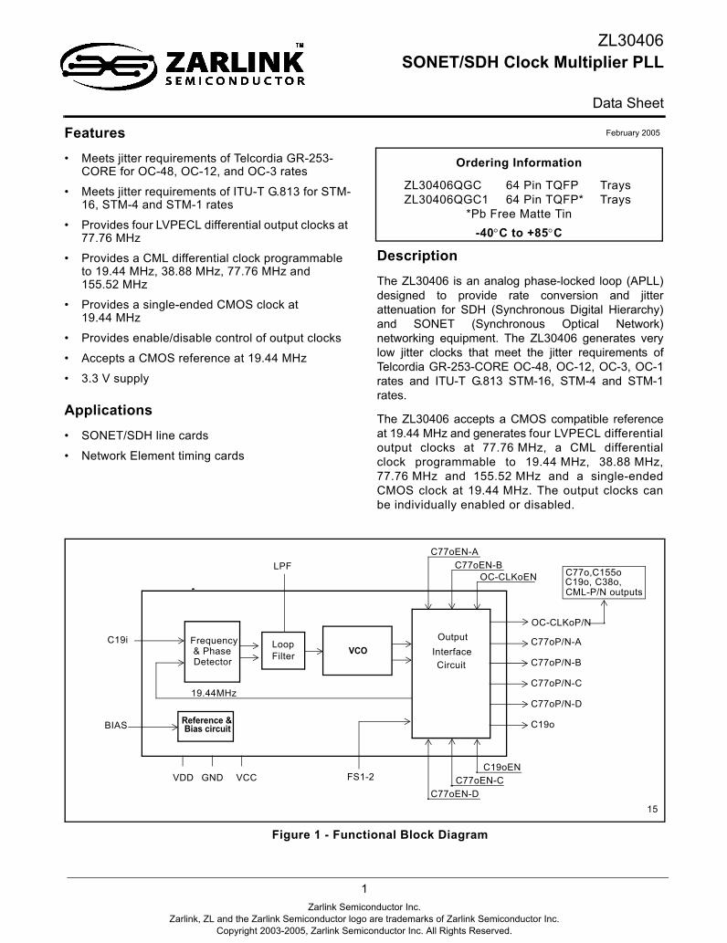
1 Zarlink Semiconductor Inc. Zarlink, ZL and the Zarlink Semiconductor logo are trademarks of Zarlink Semiconductor Inc. Copyright 2003-2005, Zarlink Semiconductor Inc. All Rights Reserved. Features • Meets jitter requirements of Telcordia GR-253- CORE for OC-48, OC-12, and OC-3 rates • Meets jitter requirements of ITU-T G.813 for STM- 16, STM-4 and STM-1 rates • Provides four LVPECL differential output clocks at 77.76 MHz • Provides a CML differential clock programmable to 19.44 MHz, 38.88 MHz, 77.76 MHz and 155.52 MHz • Provides a single-ended CMOS clock at 19.44 MHz • Provides enable/disable control of output clocks • Accepts a CMOS reference at 19.44 MHz • 3.3 V supply Applications • SONET/SDH line cards • Network Element timing cards Description The ZL30406 is an analog phase-locked loop (APLL) designed to provide rate conversion and jitter attenuation for SDH (Synchronous Digital Hierarchy) and SONET (Synchronous Optical Network) networking equipment. The ZL30406 generates very low jitter clocks that meet the jitter requirements of Telcordia GR-253-CORE OC-48, OC-12, OC-3, OC-1 rates and ITU-T G.813 STM-16, STM-4 and STM-1 rates. The ZL30406 accepts a CMOS compatible reference at 19.44 MHz and generates four LVPECL differential output clocks at 77.76 MHz, a CML differential clock programmable to 19.44 MHz, 38.88 MHz, 77.76 MHz and 155.52 MHz and a single-ended CMOS clock at 19.44 MHz. The output clocks can be individually enabled or disabled. February 2005 Ordering Information ZL30406QGC 64 Pin TQFP Trays ZL30406QGC1 64 Pin TQFP* Trays *Pb Free Matte Tin -40°C to +85°C Figure 1 - Functional Block Diagram Frequency Detector VCO C77oP/N-A Interface Circuit LPF FS1-2 C77oP/N-B C77oP/N-C VDD GND VCC C77oP/N-D C19o C19oEN OC-CLKoP/N OC-CLKoEN C155o CML-P/N outputs Loop Filter C77oEN-C C19i C77o, C19o, C38o, C77oEN-B BIAS C77oEN-A C77oEN-D & Phase Output 19.44MHz 15 Reference & Bias circuit ZL30406 SONET/SDH Clock Multiplier PLL Data Sheet
Transcript of ZL30406 SONET/SDH Clock Multiplier PLL€¦ · · 2005-05-21• SONET/SDH line cards ......
1Zarlink Semiconductor Inc.
Zarlink, ZL and the Zarlink Semiconductor logo are trademarks of Zarlink Semiconductor Inc.Copyright 2003-2005, Zarlink Semiconductor Inc. All Rights Reserved.
Features• Meets jitter requirements of Telcordia GR-253-
CORE for OC-48, OC-12, and OC-3 rates
• Meets jitter requirements of ITU-T G.813 for STM-16, STM-4 and STM-1 rates
• Provides four LVPECL differential output clocks at 77.76 MHz
• Provides a CML differential clock programmable to 19.44 MHz, 38.88 MHz, 77.76 MHz and 155.52 MHz
• Provides a single-ended CMOS clock at 19.44 MHz
• Provides enable/disable control of output clocks
• Accepts a CMOS reference at 19.44 MHz
• 3.3 V supply
Applications• SONET/SDH line cards
• Network Element timing cards
DescriptionThe ZL30406 is an analog phase-locked loop (APLL)designed to provide rate conversion and jitterattenuation for SDH (Synchronous Digital Hierarchy)and SONET (Synchronous Optical Network)networking equipment. The ZL30406 generates verylow jitter clocks that meet the jitter requirements ofTelcordia GR-253-CORE OC-48, OC-12, OC-3, OC-1rates and ITU-T G.813 STM-16, STM-4 and STM-1rates.
The ZL30406 accepts a CMOS compatible referenceat 19.44 MHz and generates four LVPECL differentialoutput clocks at 77.76 MHz, a CML differentialclock programmable to 19.44 MHz, 38.88 MHz,77.76 MHz and 155.52 MHz and a single-endedCMOS clock at 19.44 MHz. The output clocks canbe individually enabled or disabled.
February 2005
Ordering Information
ZL30406QGC 64 Pin TQFP TraysZL30406QGC1 64 Pin TQFP* Trays
*Pb Free Matte Tin-40°C to +85°C
Figure 1 - Functional Block Diagram
Frequency
DetectorVCO
C77oP/N-AInterface
Circuit
LPF
FS1-2
C77oP/N-B
C77oP/N-C
VDD GND VCC
C77oP/N-D
C19o
C19oEN
OC-CLKoP/N
OC-CLKoEN C155o
CML-P/N outputs
LoopFilter
C77oEN-C
C19i
C77o, C19o, C38o,
C77oEN-B
BIAS
C77oEN-A
C77oEN-D
& PhaseOutput
19.44MHz
15
Reference &Bias circuit
ZL30406 SONET/SDH Clock Multiplier PLL
Data Sheet
ZL30406 Data Sheet
2Zarlink Semiconductor Inc.
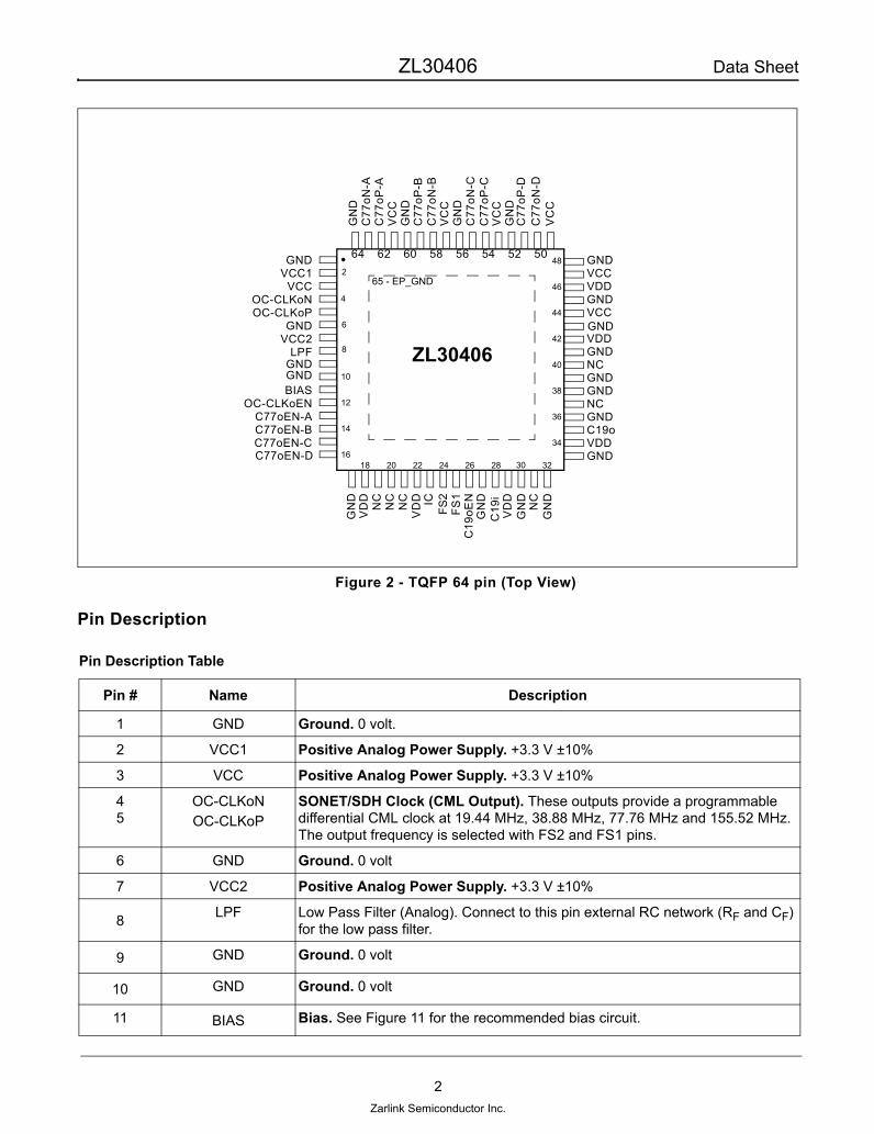
Figure 2 - TQFP 64 pin (Top View)
Pin Description
Pin Description Table
Pin # Name Description
1 GND Ground. 0 volt.
2 VCC1 Positive Analog Power Supply. +3.3 V ±10%
3 VCC Positive Analog Power Supply. +3.3 V ±10%
45
OC-CLKoNOC-CLKoP
SONET/SDH Clock (CML Output). These outputs provide a programmable differential CML clock at 19.44 MHz, 38.88 MHz, 77.76 MHz and 155.52 MHz. The output frequency is selected with FS2 and FS1 pins.
6 GND Ground. 0 volt
7 VCC2 Positive Analog Power Supply. +3.3 V ±10%
8 LPF Low Pass Filter (Analog). Connect to this pin external RC network (RF and CF) for the low pass filter.
9 GND Ground. 0 volt
10 GND Ground. 0 volt
11 BIAS Bias. See Figure 11 for the recommended bias circuit.
5052545658606264
34
36
38
40
44
46
48
42
3230282624222018
GND
VDDGNDVCC
VDD
VDDGND
GNDNCGNDGNDNCGNDC19o
VCC
G
ND
NC
C19
oEN
FS1
FS
2
ICNC
V
DD
C19
i
V
DD
NC
N
C
V
DD
GN
DV
CC
C77
oP-C
C77
oN-C
GN
DV
CC
C77
oP-B
C77
oN-B
GN
DV
CC
C77
oP-A
C77
oN-A
GN
D
C77
oP-D
C77
oN-D
VC
C
16
14
12
10
6
4
2
8
GNDVCC1
VCCOC-CLKoNOC-CLKoP
GNDVCC2
LPF
C77oEN-B
C77oEN-D
GND
BIASOC-CLKoEN
C77oEN-A
C77oEN-C
GND
G
ND
G
ND
G
ND
GNDZL30406
65 - EP_GND

ZL30406 Data Sheet
3Zarlink Semiconductor Inc.
12 OC-CLKoEN SONET/SDH Clock Enable (CMOS Input). If tied high this control pin enables the OC-CLKoP/N differential driver. Pulling this input low disables the output clock without deactivating differential drivers.
13C77oEN-A C77 Clock Output Enable A (CMOS Input). If tied high this control pin
enables the C77oP/N-A output clock. Pulling this input low disables the output clock without deactivating differential drivers.
14C77oEN-B C77 Clock Output Enable B (CMOS Input). If tied high this control pin
enables the C77oP/N-B output clock. Pulling this input low disables the output clock without deactivating differential drivers.
15C77oEN-C C77 Clock Output Enable C (CMOS Input). If tied high this control pin
enables the C77oP/N-C output clock. Pulling this input low disables the output clock without deactivating differential drivers.
16C77oEN-D C77 Clock Output Enable D (CMOS Input). If tied high this control pin
enables the C77oP/N-D output clock. Pulling this input low disables the output clock without deactivating differential drivers.
17 GND Ground. 0 volt
18 VDD Positive Digital Power Supply. +3.3 V ±10%
19 NC No internal bonding Connection. Leave unconnected.
20 NC No internal bonding Connection. Leave unconnected.
21 NC No internal bonding Connection. Leave unconnected.
22 VDD Positive Digital Power Supply. +3.3 V ±10%
23 IC Internal Connection. Connect this pin to Ground (GND).
2425
FS2FS1
Frequency Select 2-1 (CMOS Input). These inputs program the clock frequency on the OC-CLKo output. The possible output frequencies are 19.44 MHz (00), 38.88 MHz (01), 77.76 MHz (10), 155.52 MHz (11).
26 C19oEN C19o Output Enable (CMOS Input). If tied high this control pin enables the C19o output clock. Pulling this pin low forces output driver into a high impedance state.
27 GND Ground. 0 volt
28 C19i C19 Reference Input (CMOS Input). This pin is a single-ended input reference source used for synchronization. This pin accepts 19.44 MHz.
29 VDD Positive Digital Power Supply. +3.3 V ±10%
30 GND Ground. 0 volt
31 NC No internal bonding Connection. Leave unconnected.
32 GND Ground. 0 volt.
33 GND Ground. 0 volt
34 VDD Positive Digital Power Supply. +3.3 V ±10%
35 C19o C19 Clock Output (CMOS Output). This pin provides a single-ended CMOS clock at 19.44 MHz.
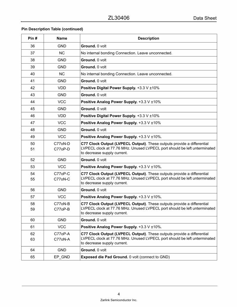
Pin Description Table (continued)
Pin # Name Description
ZL30406 Data Sheet
4Zarlink Semiconductor Inc.
36 GND Ground. 0 volt
37 NC No internal bonding Connection. Leave unconnected.
38 GND Ground. 0 volt
39 GND Ground. 0 volt
40 NC No internal bonding Connection. Leave unconnected.
41 GND Ground. 0 volt
42 VDD Positive Digital Power Supply. +3.3 V ±10%
43 GND Ground. 0 volt
44 VCC Positive Analog Power Supply. +3.3 V ±10%
45 GND Ground. 0 volt
46 VDD Positive Digital Power Supply. +3.3 V ±10%
47 VCC Positive Analog Power Supply. +3.3 V ±10%
48 GND Ground. 0 volt
49 VCC Positive Analog Power Supply. +3.3 V ±10%.
5051
C77oN-DC77oP-D
C77 Clock Output (LVPECL Output). These outputs provide a differential LVPECL clock at 77.76 MHz. Unused LVPECL port should be left unterminated to decrease supply current.
52 GND Ground. 0 volt
53 VCC Positive Analog Power Supply. +3.3 V ±10%.
5455
C77oP-CC77oN-C
C77 Clock Output (LVPECL Output). These outputs provide a differential LVPECL clock at 77.76 MHz. Unused LVPECL port should be left unterminated to decrease supply current.
56 GND Ground. 0 volt
57 VCC Positive Analog Power Supply. +3.3 V ±10%.
5859
C77oN-BC77oP-B
C77 Clock Output (LVPECL Output). These outputs provide a differential LVPECL clock at 77.76 MHz. Unused LVPECL port should be left unterminated to decrease supply current.
60 GND Ground. 0 volt
61 VCC Positive Analog Power Supply. +3.3 V ±10%.
6263
C77oP-AC77oN-A
C77 Clock Output (LVPECL Output). These outputs provide a differential LVPECL clock at 77.76 MHz. Unused LVPECL port should be left unterminated to decrease supply current.
64 GND Ground. 0 volt
65 EP_GND Exposed die Pad Ground. 0 volt (connect to GND)
Pin Description Table (continued)
Pin # Name Description
ZL30406 Data Sheet
5Zarlink Semiconductor Inc.
1.0 Functional DescriptionThe ZL30406 is an analog phased-locked loop which provides rate conversion and jitter attenuation forSONET/SDH OC-48/STM-16, OC-12/STM-4 and OC-3/STM-1 applications. A functional block diagram of theZL30406 is shown in Figure 1 and a brief description is presented in the following sections.
1.1 Frequency/Phase Detector
The Frequency/Phase Detector compares the frequency/phase of the input reference signal with the feedbacksignal from the Frequency Divider circuit and provides an error signal corresponding to the frequency/phasedifference between the two. This error signal is passed to the Loop Filter circuit and averaged to control theVCO frequency.
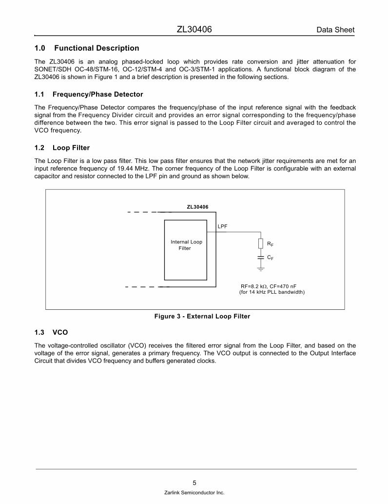
1.2 Loop Filter
The Loop Filter is a low pass filter. This low pass filter ensures that the network jitter requirements are met for aninput reference frequency of 19.44 MHz. The corner frequency of the Loop Filter is configurable with an externalcapacitor and resistor connected to the LPF pin and ground as shown below.
Figure 3 - External Loop Filter
1.3 VCO
The voltage-controlled oscillator (VCO) receives the filtered error signal from the Loop Filter, and based on thevoltage of the error signal, generates a primary frequency. The VCO output is connected to the Output InterfaceCircuit that divides VCO frequency and buffers generated clocks.
RF
CF
Internal Loop Filter
ZL30406
LPF
RF=8.2 kΩ, CF=470 nF(for 14 kHz PLL bandwidth)
ZL30406 Data Sheet
6Zarlink Semiconductor Inc.
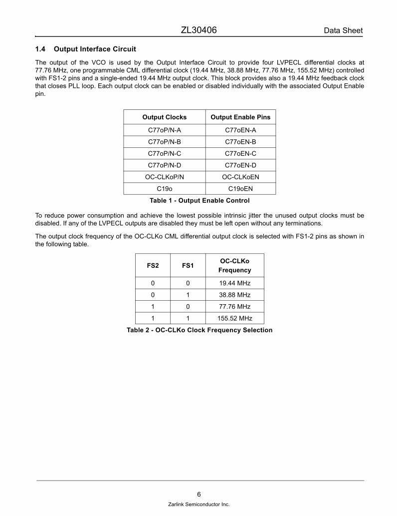
1.4 Output Interface Circuit
The output of the VCO is used by the Output Interface Circuit to provide four LVPECL differential clocks at77.76 MHz, one programmable CML differential clock (19.44 MHz, 38.88 MHz, 77.76 MHz, 155.52 MHz) controlledwith FS1-2 pins and a single-ended 19.44 MHz output clock. This block provides also a 19.44 MHz feedback clockthat closes PLL loop. Each output clock can be enabled or disabled individually with the associated Output Enablepin.
To reduce power consumption and achieve the lowest possible intrinsic jitter the unused output clocks must bedisabled. If any of the LVPECL outputs are disabled they must be left open without any terminations.
The output clock frequency of the OC-CLKo CML differential output clock is selected with FS1-2 pins as shown inthe following table.
Output Clocks Output Enable Pins
C77oP/N-A C77oEN-A
C77oP/N-B C77oEN-B
C77oP/N-C C77oEN-C
C77oP/N-D C77oEN-D
OC-CLKoP/N OC-CLKoEN
C19o C19oEN
Table 1 - Output Enable Control
FS2 FS1OC-CLKo Frequency
0 0 19.44 MHz
0 1 38.88 MHz
1 0 77.76 MHz
1 1 155.52 MHz
Table 2 - OC-CLKo Clock Frequency Selection
ZL30406 Data Sheet
7Zarlink Semiconductor Inc.
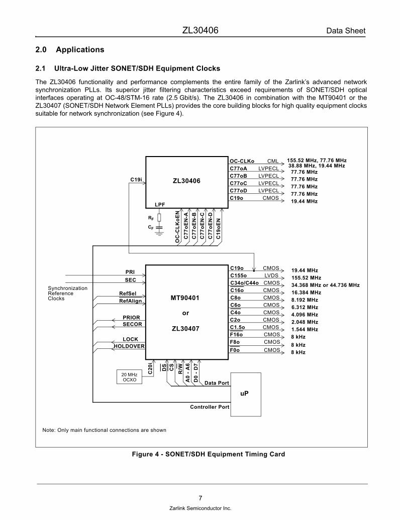
2.0 Applications
2.1 Ultra-Low Jitter SONET/SDH Equipment Clocks
The ZL30406 functionality and performance complements the entire family of the Zarlink’s advanced networksynchronization PLLs. Its superior jitter filtering characteristics exceed requirements of SONET/SDH opticalinterfaces operating at OC-48/STM-16 rate (2.5 Gbit/s). The ZL30406 in combination with the MT90401 or theZL30407 (SONET/SDH Network Element PLLs) provides the core building blocks for high quality equipment clockssuitable for network synchronization (see Figure 4).
Figure 4 - SONET/SDH Equipment Timing Card
MT90401
ZL30406
OC-CLKo CML 38.88 MHz, 19.44 MHz
77.76 MHz19.44 MHz
C77oA LVPECLC77oB LVPECLC77oC LVPECLC77oD LVPECLC19o CMOS
C19i
C19o CMOSC155o LVDSC34o/C44o CMOSC16o CMOSC8o CMOSC6o CMOS
19.44 MHz
C2o CMOSC1.5o CMOS
F8o CMOSF0o CMOS
77.76 MHz77.76 MHz77.76 MHz
155.52 MHz
C4o CMOS
34.368 MHz or 44.736 MHz16.384 MHz8.192 MHz6.312 MHz4.096 MHz2.048 MHz1.544 MHz
8 kHz8 kHz
PRISEC
PRIORSECOR
LOCKHOLDOVER
RefSelRefAlign
RF
LPF
CF
OC
-CL K
oEN
155.52 MHz, 77.76 MHz
C77
oEN
-AC
77oE
N-B
C77
o EN
-CC
77oE
N-D
C1 9
oEN
DS
CS
R/W
A0
- A6
D0
- D7
uPData Port
Controller Port
SynchronizationReferenceClocks
Note: Only main functional connections are shown
20 MHz C20
i
F16o CMOS
OCXO
8 kHz
or
ZL30407
ZL30406 Data Sheet
8Zarlink Semiconductor Inc.
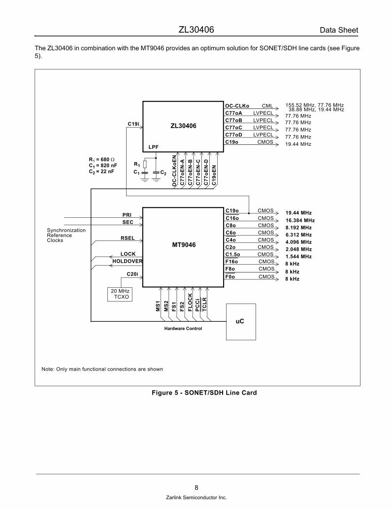
The ZL30406 in combination with the MT9046 provides an optimum solution for SONET/SDH line cards (see Figure5).
Figure 5 - SONET/SDH Line Card
MT9046
ZL30406
OC-CLKo CML 38.88 MHz, 19.44 MHz
77.76 MHz19.44 MHz
C77oA LVPECLC77oB LVPECLC77oC LVPECLC77oD LVPECLC19o CMOS
C19i
C19o CMOSC16o CMOSC8o CMOSC6o CMOS
19.44 MHz
C2o CMOSC1.5o CMOS
F8o CMOSF0o CMOS
77.76 MHz77.76 MHz77.76 MHz
C4o CMOS
16.384 MHz8.192 MHz6.312 MHz4.096 MHz2.048 MHz1.544 MHz
8 kHz8 kHz
PRISEC
LOCKHOLDOVER
RSEL
R1
LPF
C1O
C-C
LKo E
N
155.52 MHz, 77.76 MHz
C77
oEN
-AC
77oE
N-B
C77
o EN
-CC
77oE
N-D
C1 9
oEN
MS
1
FS2
FLO
CK
uC
SynchronizationReferenceClocks
Note: Only main functional connections are shown
20 MHz
F16o CMOS
TCXO
8 kHz
C2
R1 = 680 ΩC1 = 820 nFC2 = 22 nF
C20i
MS
2FS
1
PC
Ci
Hardware Control
TCLR
ZL30406 Data Sheet
9Zarlink Semiconductor Inc.
2.2 Recommended Interface circuit
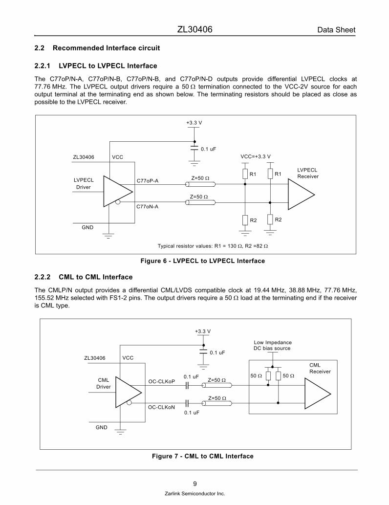
2.2.1 LVPECL to LVPECL Interface
The C77oP/N-A, C77oP/N-B, C77oP/N-B, and C77oP/N-D outputs provide differential LVPECL clocks at77.76 MHz. The LVPECL output drivers require a 50 Ω termination connected to the VCC-2V source for eachoutput terminal at the terminating end as shown below. The terminating resistors should be placed as close aspossible to the LVPECL receiver.
Figure 6 - LVPECL to LVPECL Interface
2.2.2 CML to CML Interface
The CMLP/N output provides a differential CML/LVDS compatible clock at 19.44 MHz, 38.88 MHz, 77.76 MHz,155.52 MHz selected with FS1-2 pins. The output drivers require a 50 Ω load at the terminating end if the receiveris CML type.
Figure 7 - CML to CML Interface
LVPECL
LVPECL
ZL30406
Z=50 Ω
Z=50 Ω
C77oP-A
C77oN-A
Receiver
GND
Typical resistor values: R1 = 130 Ω, R2 =82 Ω
R1
R2
VCC=+3.3 V
R1
R2
VCC0.1 uF
+3.3 V
Driver
ZL30406
CML Z=50 Ω
CML
50 ΩOC-CLKoP
OC-CLKoN
Driver
GND
VCC
Receiver
0.1 uF
+3.3 V
50 Ω
Z=50 Ω
0.1 uF
0.1 uF
Low ImpedanceDC bias source
ZL30406 Data Sheet
10Zarlink Semiconductor Inc.
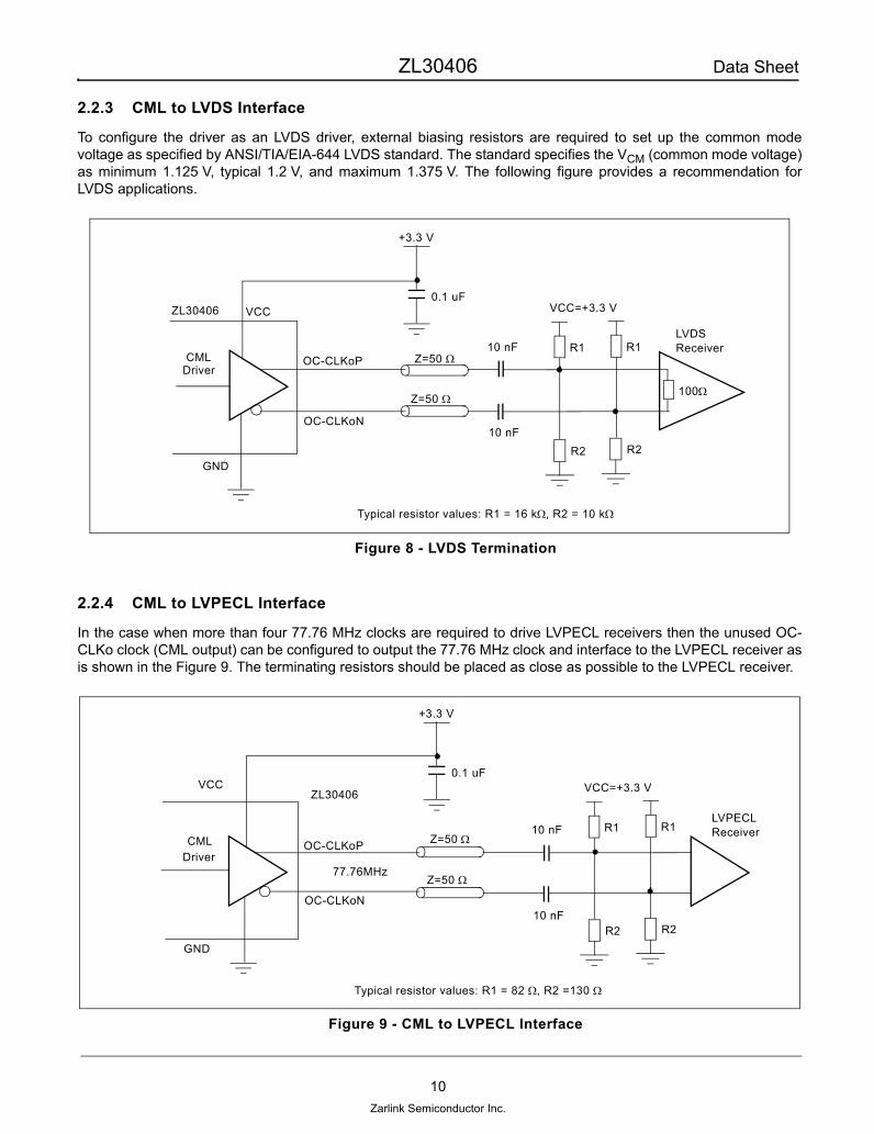
2.2.3 CML to LVDS Interface
To configure the driver as an LVDS driver, external biasing resistors are required to set up the common modevoltage as specified by ANSI/TIA/EIA-644 LVDS standard. The standard specifies the VCM (common mode voltage)as minimum 1.125 V, typical 1.2 V, and maximum 1.375 V. The following figure provides a recommendation forLVDS applications.
Figure 8 - LVDS Termination
2.2.4 CML to LVPECL Interface
In the case when more than four 77.76 MHz clocks are required to drive LVPECL receivers then the unused OC-CLKo clock (CML output) can be configured to output the 77.76 MHz clock and interface to the LVPECL receiver asis shown in the Figure 9. The terminating resistors should be placed as close as possible to the LVPECL receiver.
Figure 9 - CML to LVPECL Interface
ZL30406
CML Z=50 Ω
Z=50 Ω
Driver
0.1 uF
+3.3 V
GND
VCC
LVDS10 nF
10 nF
ReceiverR1
R2
VCC=+3.3 V
R1
R2
100Ω
Typical resistor values: R1 = 16 kΩ, R2 = 10 kΩ
OC-CLKoP
OC-CLKoN
LVPECL
CML
ZL30406
Z=50 Ω
Z=50 Ω
Receiver
GND
Typical resistor values: R1 = 82 Ω, R2 =130 Ω
R1
R2
VCC=+3.3 V
R1
R2
VCC0.1 uF
+3.3 V
Driver
10 nF
10 nFOC-CLKoP
OC-CLKoN
77.76MHz
ZL30406 Data Sheet
11Zarlink Semiconductor Inc.
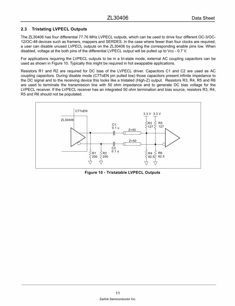
2.3 Tristating LVPECL Outputs
The ZL30406 has four differential 77.76 MHz LVPECL outputs, which can be used to drive four different OC-3/OC-12/OC-48 devices such as framers, mappers and SERDES. In the case where fewer than four clocks are required,a user can disable unused LVPECL outputs on the ZL30406 by pulling the corresponding enable pins low. Whendisabled, voltage at the both pins of the differential LVPECL output will be pulled up to Vcc - 0.7 V.
For applications requiring the LVPECL outputs to be in a tri-state mode, external AC coupling capacitors can beused as shown in Figure 10. Typically this might be required in hot swappable applications.
Resistors R1 and R2 are required for DC bias of the LVPECL driver. Capacitors C1 and C2 are used as ACcoupling capacitors. During disable mode (C77oEN pin pulled low) those capacitors present infinite impedance tothe DC signal and to the receiving device this looks like a tristated (High-Z) output. Resistors R3, R4, R5 and R6are used to terminate the transmission line with 50 ohm impedance and to generate DC bias voltage for theLVPECL receiver. If the LVPECL receiver has an integrated 50 ohm termination and bias source, resistors R3, R4,R5 and R6 should not be populated.
Figure 10 - Tristatable LVPECL Outputs
Z=50
Z=50
C77oEN
ZL30406
0.1 uC1
0.1 uC2
R482.5
R682.5
R5127
R3127
R1200
R2200
3.3 V 3.3 V
ZL30406 Data Sheet
12Zarlink Semiconductor Inc.
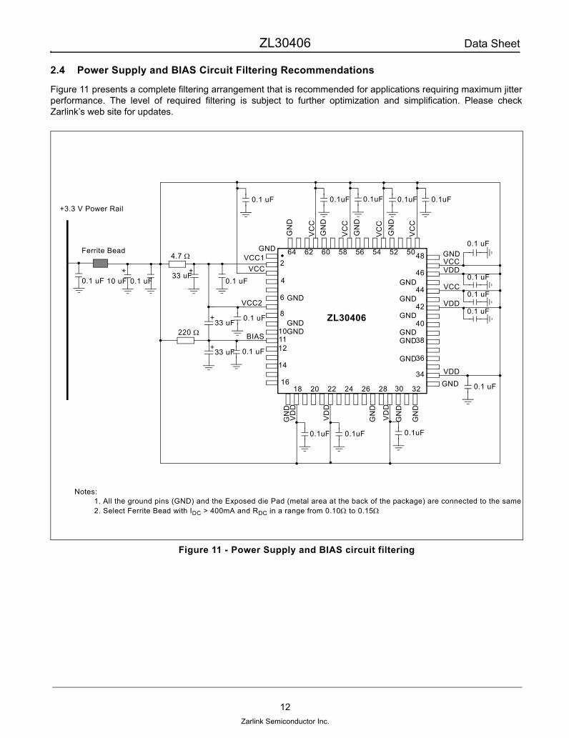
2.4 Power Supply and BIAS Circuit Filtering Recommendations
Figure 11 presents a complete filtering arrangement that is recommended for applications requiring maximum jitterperformance. The level of required filtering is subject to further optimization and simplification. Please checkZarlink’s web site for updates.
Figure 11 - Power Supply and BIAS circuit filtering
5052545658606264
34
40
44
46
48
42
3230282624222018
GND
VDDGND VCC
VDD
VDD
GND
GNDGND
GND
VCC
VD
D
VD
D
VD
D
GN
DV
CC
GN
DV
CC
GN
DV
CC
GN
D
VC
C
16
14
12
10
6
4
2
8
GNDVCC1
GNDVCC2
GNDGND
GND
GN
D
GN
D
GN
D
0.1uF 0.1uF 0.1uF 0.1uF
0.1 uFFerrite Bead
0.1 uF33 uF
0.1uF 0.1uF 0.1uF
0.1 uF
0.1 uF
0.1 uF
0.1 uF
Notes:1. All the ground pins (GND) and the Exposed die Pad (metal area at the back of the package) are connected to the same 2. Select Ferrite Bead with IDC > 400mA and RDC in a range from 0.10Ω to 0.15Ω
+3.3 V Power Rail
ZL30406
0.1 uF G
ND
GND
BIAS220 Ω11
VCC
0.1 uF
36
38
+0.1 uF
4.7 Ω
10 uF+
+33 uF
+33 uF
0.1 uF
0.1 uF
ZL30406 Data Sheet
13Zarlink Semiconductor Inc.
3.0 Characteristics
† Voltages are with respect to ground unless otherwise stated.‡ Exceeding these values may cause permanent damage. Functional operation under these conditions is not implied.
† Voltages are with respect to ground unless otherwise stated.‡ Typical figures are for design aid only: not guaranteed and not subject to production testing.‡
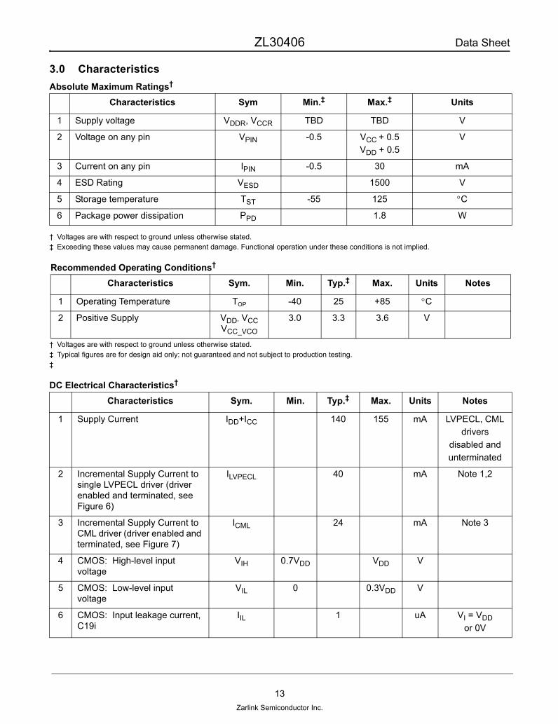
Absolute Maximum Ratings†
Characteristics Sym Min.‡ Max.‡ Units
1 Supply voltage VDDR, VCCR TBD TBD V
2 Voltage on any pin VPIN -0.5 VCC + 0.5VDD + 0.5
V
3 Current on any pin IPIN -0.5 30 mA
4 ESD Rating VESD 1500 V
5 Storage temperature TST -55 125 °C
6 Package power dissipation PPD 1.8 W
Recommended Operating Conditions†
Characteristics Sym. Min. Typ.‡ Max. Units Notes
1 Operating Temperature TOP -40 25 +85 °C
2 Positive Supply VDD, VCCVCC_VCO
3.0 3.3 3.6 V
DC Electrical Characteristics†
Characteristics Sym. Min. Typ.‡ Max. Units Notes
1 Supply Current IDD+ICC 140 155 mA LVPECL, CML drivers
disabled and unterminated
2 Incremental Supply Current to single LVPECL driver (driver enabled and terminated, see Figure 6)
ILVPECL 40 mA Note 1,2
3 Incremental Supply Current to CML driver (driver enabled and terminated, see Figure 7)
ICML 24 mA Note 3
4 CMOS: High-level input voltage
VIH 0.7VDD VDD V
5 CMOS: Low-level input voltage
VIL 0 0.3VDD V
6 CMOS: Input leakage current, C19i
IIL 1 uA VI = VDD or 0V
ZL30406 Data Sheet
14Zarlink Semiconductor Inc.
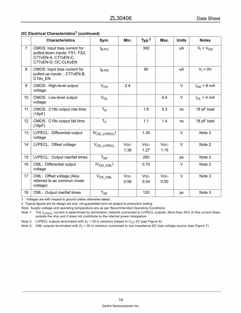
† : Voltages are with respect to ground unless otherwise stated.‡ :Typical figures are for design aid only: not guaranteed and not subject to production testing.Note: Supply voltage and operating temperature are as per Recommended Operating ConditionsNote 1: The ILVPECL current is determined by termination network connected to LVPECL outputs. More than 25% of this current flows
outside the chip and it does not contribute to the internal power dissipation. Note 2: LVPECL outputs terminated with ZT = 50 Ω resistors biased to VCC-2V (see Figure 6)Note 3: CML outputs terminated with ZT = 50 Ω resistors connected to low impedance DC bias voltage source (see Figure 7)
7 CMOS: Input bias current for pulled-down inputs: FS1, FS2, C77oEN-A, C77oEN-C, C77oEN-D, OC-CLKoEN
IB-PU 300 uA VI = VDD
8 CMOS: Input bias current for pulled-up inputs: , C77oEN-B, C19o_EN
IB-PD 90 uA VI = 0V
9 CMOS: High-level output voltage
VOH 2.4 V IOH = 8 mA
10 CMOS: Low-level output voltage
VOL 0.4 V IOL = 4 mA
11 CMOS: C19o output rise time (18pF)
TR 1.8 3.3 ns 18 pF load
12 CMOS: C19o output fall time (18pF)
TF 1.1 1.4 ns 18 pF load
13 LVPECL: Differential output voltage
IVOD_LVPECLI 1.30 V Note 2
14 LVPECL: Offset voltage VOS_LVPECL Vcc-1.38
Vcc-1.27
Vcc-1.15
V Note 2
15 LVPECL: Output rise/fall times TRF 260 ps Note 2
16 CML: Differential output voltage
IVOD_CMLI 0.70 V Note 3
17 CML: Offset voltage (Also referred to as common mode voltage)
VOS_CML Vcc-0.58
Vcc-0.54
Vcc-0.50
V Note 3
18 CML: Output rise/fall times TRF 120 ps Note 3
DC Electrical Characteristics† (continued)Characteristics Sym. Min. Typ.‡ Max. Units Notes
ZL30406 Data Sheet
15Zarlink Semiconductor Inc.
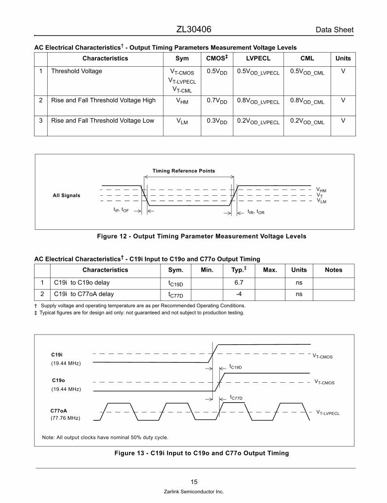
Figure 12 - Output Timing Parameter Measurement Voltage Levels
† Supply voltage and operating temperature are as per Recommended Operating Conditions.‡ Typical figures are for design aid only: not guaranteed and not subject to production testing.
Figure 13 - C19i Input to C19o and C77o Output Timing
AC Electrical Characteristics† - Output Timing Parameters Measurement Voltage LevelsCharacteristics Sym CMOS‡ LVPECL CML Units
1 Threshold Voltage VT-CMOSVT-LVPECL
VT-CML
0.5VDD 0.5VOD_LVPECL 0.5VOD_CML V
2 Rise and Fall Threshold Voltage High VHM 0.7VDD 0.8VOD_LVPECL 0.8VOD_CML V
3 Rise and Fall Threshold Voltage Low VLM 0.3VDD 0.2VOD_LVPECL 0.2VOD_CML V
AC Electrical Characteristics† - C19i Input to C19o and C77o Output TimingCharacteristics Sym. Min. Typ.‡ Max. Units Notes
1 C19i to C19o delay tC19D 6.7 ns
2 C19i to C77oA delay tC77D -4 ns
VTAll SignalsVHM
VLM
tIF, tOF tIR, tOR
Timing Reference Points
C77oA VT-LVPECL
C19i VT-CMOS(19.44 MHz) tC19D
C19o VT-CMOS(19.44 MHz)
tC77D
(77.76 MHz)
Note: All output clocks have nominal 50% duty cycle.
ZL30406 Data Sheet
16Zarlink Semiconductor Inc.
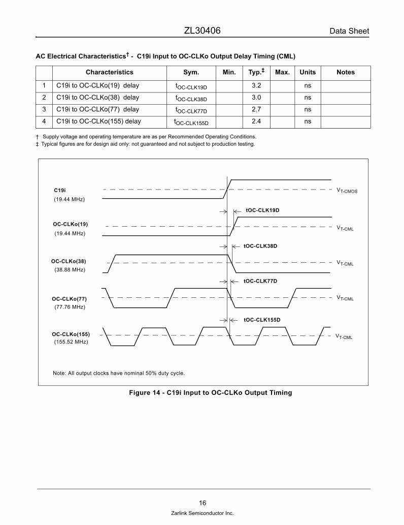
AC Electrical Characteristics† - C19i Input to OC-CLKo Output Delay Timing (CML)
† Supply voltage and operating temperature are as per Recommended Operating Conditions.‡ Typical figures are for design aid only: not guaranteed and not subject to production testing.
Figure 14 - C19i Input to OC-CLKo Output Timing
Characteristics Sym. Min. Typ.‡ Max. Units Notes
1 C19i to OC-CLKo(19) delay tOC-CLK19D 3.2 ns
2 C19i to OC-CLKo(38) delay tOC-CLK38D 3.0 ns
3 C19i to OC-CLKo(77) delay tOC-CLK77D 2.7 ns
4 C19i to OC-CLKo(155) delay tOC-CLK155D 2.4 ns
OC-CLKo(38) VT-CML
C19i VT-CMOS
(19.44 MHz)
tOC-CLK19D
OC-CLKo(19) VT-CML(19.44 MHz)
tOC-CLK38D
(38.88 MHz)
OC-CLKo(155) VT-CML (155.52 MHz)
OC-CLKo(77) VT-CML
(77.76 MHz)
tOC-CLK77D
tOC-CLK155D
Note: All output clocks have nominal 50% duty cycle.
ZL30406 Data Sheet
17Zarlink Semiconductor Inc.
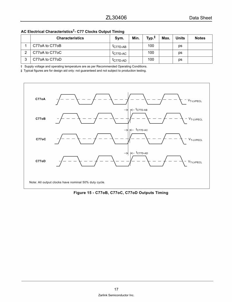
† Supply voltage and operating temperature are as per Recommended Operating Conditions.‡ Typical figures are for design aid only: not guaranteed and not subject to production testing.
Figure 15 - C77oB, C77oC, C77oD Outputs Timing
AC Electrical Characteristics†- C77 Clocks Output TimingCharacteristics Sym. Min. Typ.‡ Max. Units Notes
1 C77oA to C77oB tC77D-AB 100 ps
2 C77oA to C77oC tC77D-AC 100 ps
3 C77oA to C77oD tC77D-AD 100 ps
C77oD VT-LVPECL
C77oC
tC77D-AB
C77oB
C77oA
VT-LVPECL
VT-LVPECL
VT-LVPECL
tC77D-AC
tC77D-AD
Note: All output clocks have nominal 50% duty cycle.
ZL30406 Data Sheet
18Zarlink Semiconductor Inc.
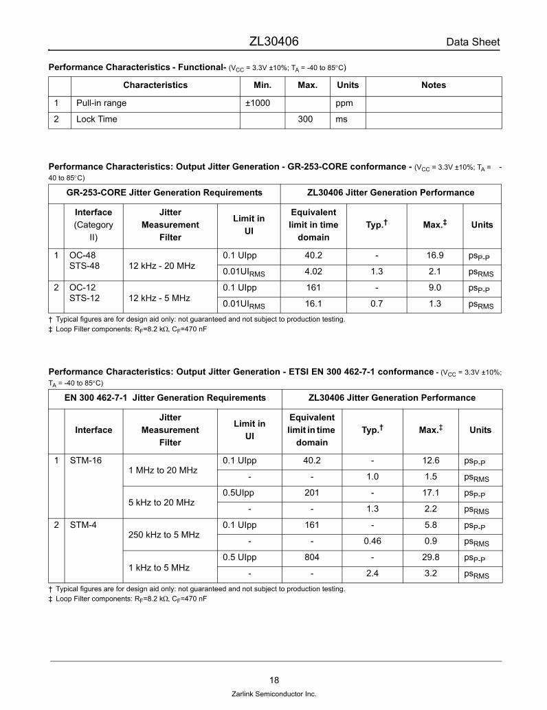
Performance Characteristics - Functional- (VCC = 3.3V ±10%; TA = -40 to 85°C)
† Typical figures are for design aid only: not guaranteed and not subject to production testing.‡ Loop Filter components: RF=8.2 kΩ, CF=470 nF
† Typical figures are for design aid only: not guaranteed and not subject to production testing.‡ Loop Filter components: RF=8.2 kΩ, CF=470 nF
Characteristics Min. Max. Units Notes
1 Pull-in range ±1000 ppm
2 Lock Time 300 ms
Performance Characteristics: Output Jitter Generation - GR-253-CORE conformance - (VCC = 3.3V ±10%; TA = -40 to 85°C)
GR-253-CORE Jitter Generation Requirements ZL30406 Jitter Generation Performance
Interface(Category
II)
JitterMeasurement
Filter
Limit inUI
Equivalent limit in time
domainTyp.† Max.‡ Units
1 OC-48STS-48 12 kHz - 20 MHz
0.1 UIpp 40.2 - 16.9 psP-P
0.01UIRMS 4.02 1.3 2.1 psRMS
2 OC-12STS-12 12 kHz - 5 MHz
0.1 UIpp 161 - 9.0 psP-P
0.01UIRMS 16.1 0.7 1.3 psRMS
Performance Characteristics: Output Jitter Generation - ETSI EN 300 462-7-1 conformance - (VCC = 3.3V ±10%;TA = -40 to 85°C)
EN 300 462-7-1 Jitter Generation Requirements ZL30406 Jitter Generation Performance
InterfaceJitter
Measurement Filter
Limit inUI
Equivalent limit in time
domainTyp.† Max.‡ Units
1 STM-161 MHz to 20 MHz
0.1 UIpp 40.2 - 12.6 psP-P
- - 1.0 1.5 psRMS
5 kHz to 20 MHz0.5UIpp 201 - 17.1 psP-P
- - 1.3 2.2 psRMS
2 STM-4250 kHz to 5 MHz
0.1 UIpp 161 - 5.8 psP-P
- - 0.46 0.9 psRMS
1 kHz to 5 MHz0.5 UIpp 804 - 29.8 psP-P
- - 2.4 3.2 psRMS
ZL30406 Data Sheet
19Zarlink Semiconductor Inc.
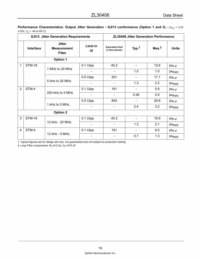
† Typical figures are for design aid only: not guaranteed and not subject to production testing.‡ Loop Filter components: RF=8.2 kΩ, CF=470 nF
Performance Characteristics: Output Jitter Generation - G.813 conformance (Option 1 and 2) - (VCC = 3.3V±10%; TA = -40 to 85°C)
G.813 Jitter Generation Requirements ZL30406 Jitter Generation Performance
InterfaceJitter
Measurement Filter
Limit inUI
Equivalent limit in time domain Typ.† Max.‡ Units
Option 1
1 STM-161 MHz to 20 MHz
0.1 UIpp 40.2 - 12.6 psP-P
- - 1.0 1.5 psRMS
5 kHz to 20 MHz0.5 UIpp 201 - 17.1 psP-P
- - 1.3 2.2 psRMS
2 STM-4250 kHz to 5 MHz
0.1 UIpp 161 - 5.8 psP-P
- - 0.46 0.9 psRMS
1 kHz to 5 MHz0.5 UIpp 804 - 29.8 psP-P
- - 2.4 3.2 psRMS
Option 2
3 STM-1612 kHz - 20 MHz
0.1 UIpp 40.2 - 16.9 psP-P
- - 1.3 2.1 psRMS
4 STM-412 kHz - 5 MHz
0.1 UIpp 161 - 9.0 psP-P
- - 0.7 1.3 psRMS
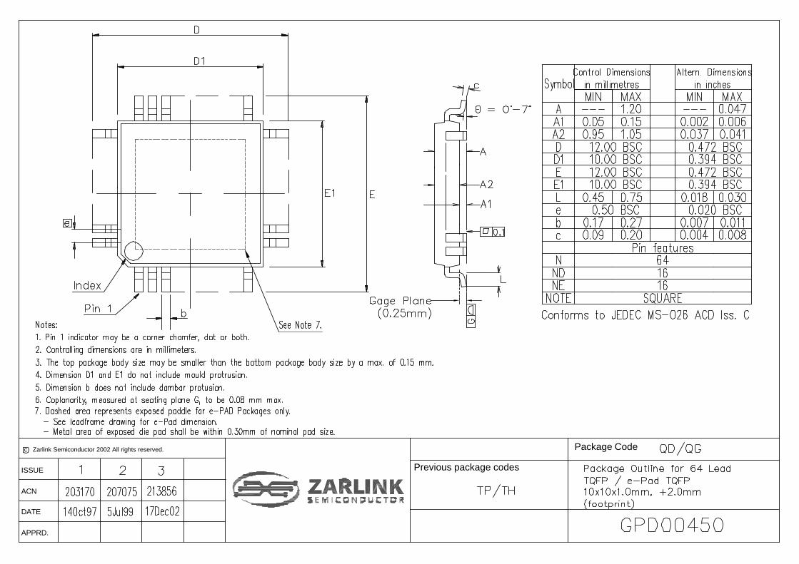
c Zarlink Semiconductor 2002 All rights reserved.
APPRD.
ISSUE
DATE
ACN
Package Code
Previous package codes
www.zarlink.com
Information relating to products and services furnished herein by Zarlink Semiconductor Inc. or its subsidiaries (collectively “Zarlink”) is believed to be reliable.However, Zarlink assumes no liability for errors that may appear in this publication, or for liability otherwise arising from the application or use of any suchinformation, product or service or for any infringement of patents or other intellectual property rights owned by third parties which may result from such application oruse. Neither the supply of such information or purchase of product or service conveys any license, either express or implied, under patents or other intellectualproperty rights owned by Zarlink or licensed from third parties by Zarlink, whatsoever. Purchasers of products are also hereby notified that the use of product incertain ways or in combination with Zarlink, or non-Zarlink furnished goods or services may infringe patents or other intellectual property rights owned by Zarlink.
This publication is issued to provide information only and (unless agreed by Zarlink in writing) may not be used, applied or reproduced for any purpose nor form partof any order or contract nor to be regarded as a representation relating to the products or services concerned. The products, their specifications, services and otherinformation appearing in this publication are subject to change by Zarlink without notice. No warranty or guarantee express or implied is made regarding thecapability, performance or suitability of any product or service. Information concerning possible methods of use is provided as a guide only and does not constituteany guarantee that such methods of use will be satisfactory in a specific piece of equipment. It is the user’s responsibility to fully determine the performance andsuitability of any equipment using such information and to ensure that any publication or data used is up to date and has not been superseded. Manufacturing doesnot necessarily include testing of all functions or parameters. These products are not suitable for use in any medical products whose failure to perform may result insignificant injury or death to the user. All products and materials are sold and services provided subject to Zarlink’s conditions of sale which are available on request.
Purchase of Zarlink’s I2C components conveys a licence under the Philips I2C Patent rights to use these components in and I2C System, provided that the systemconforms to the I2C Standard Specification as defined by Philips.
Zarlink, ZL and the Zarlink Semiconductor logo are trademarks of Zarlink Semiconductor Inc.
Copyright Zarlink Semiconductor Inc. All Rights Reserved.
TECHNICAL DOCUMENTATION - NOT FOR RESALE
For more information about all Zarlink productsvisit our Web Site at