Z r ~~~~~~~~~~~~~~~~~~~~~~~~~~~r - Nc State … for TransmissionLineDesignonMCMsusing...
2
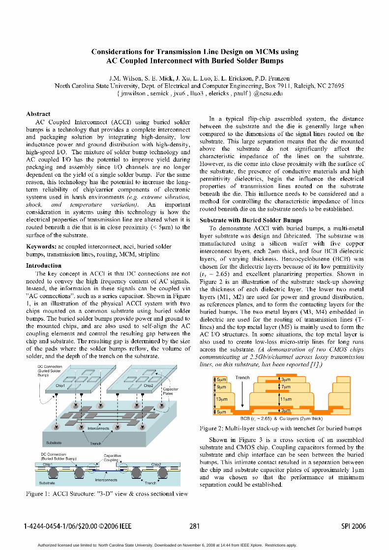
Considerations for Transmission Line Design on MCMs using AC Coupled Interconnect with Buried Solder Bumps J.M. Wilson, S. E. Mick, J. Xu, L. Luo, E. L. Erickson, P.D. Franzon North Carolina State University, Dept. of Electrical and Computer Engineering, Box 791 1, Raleigh, NC 27695 { jmwilson, semick , jxu6, lluo3 , elericks , paulf } @ncsu.edu Abstract AC Coupled Interconnect (ACCI) using buried solder In a typical flip-chip assembled system, the distance bumps is a technology that provides a complete interconnect between the substrate and the die is generally large when and packaging solution by integrating high-density, low compared to the dimensions of the signal lines routed on the inductance power and ground distribution with high-density substrate. This large separation means that the die mounted high-speed I/O. The mixture of solder bump technology and above the substrate do not significantly affect the AC coupled I/O has the potential to improve yield during characteristic impedance of the lines on the substrate. .cananasmysn /channels are no longer However, as die come into close proximity with the surface of packaging and aseml since I/O. . .the substrate, the presence of conductive materials and high dependent on the yield of a single solder bump. For the same ' . reason, this technology has the potential to increase the long- ppert ie lectra is,ion hes ifutenc the elctrical term reliability of chip/carrier components of electronic p o beneath the die. This influence needs to be considered and a systems used in harsh environments (e.g. extreme vibration, meho fo cotoln.h hrceitcipdneo ie shock,and temperature variation). An imotn method for controlling the characteristic impedance of lines .'shok,an temprure tio An impor tan routed beneath die on the substrate needs to be established. consideration in systems using this technology iS how the electrical properties of transmission line are altered when it is Substrate with Buried Solder Bumps routed beneath a die that is in close proximity (< 5 tm) to the To demonstrate ACCI with buried bumps, a multi-metal surface of the substrate. layer substrate was design and fabricated. The substrate was Keywords: ac coupled interconnect, acci, buried solder manufactured using a silicon wafer with five copper transmission lines, routing, MCM, stripline interconnect layers, each 2 tm thick, and four BCB dielectric layers, of varying thickness. Benzocyclobutene (BCB) was Introduction chosen for the dielectric layers because of its low permittivity The key concept in ACCI is that DC connections are not (Er - 2.65) and excellent planarizing properties. Shown in needed to convey the high frequency content of AC signals. Figure 2 is an illustration of the substrate stack-up showing Instead, the information in these signals can be coupled via the thickness of each dielectric layer. The lower two metal "AC connections", such as a series capacitor. Shown in Figure layers (MI, M2) are used for power and ground distribution, 1, is an illustration of the physical ACCI system with two as references planes, and to form the contacting layers for the chips mounted on a common substrate using buried solder buried bumps. The two metal layers (M3, M4) embedded in bumps. The buried solder bumps provide power and ground to dielectric are used for the routing of transmission lines (T- the mounted chips, and are also used to self-align the AC lines) and the top metal layer (M5) is mainly used to form the coupling elements and control the resulting gap between the AC I/O structures. In some situations, the top metal layer is chip and substrate. The resulting gap is determined by the size also used to create low-loss micro-strip lines for long runs of the pads where the solder bumps reflow, the volume of across the substrate. (A demonstration of two CMOS chips solder, and the depth of the trench on the substrate. communicating at 2.5Gb/s/channel across lossy transmission DC Connection lines, on this substrate, has been reported [1].) (Buried So der Bump) / i; g Z Bump m __Trench 37m Chipi ~~~~~~~~~Chip297m I _ t__ G Capacitor I ~~~~~ w w ~~~~~~~~~~Plates r _r _~~~~~~~~~~~~~~~~~~~~~~~~~~~r BCB (e> 2.65) & Cu layers 2[trn thick) interconne Figure 2: Multi-layer stack-up with trenches for buried bumps ilb-lrgi l! | ~~~~~~Shownin Figure 3 is a cross section of an assemnbled DC Connection Capacitive substrate and chip interface can be seen between the buried _Bre SodrBm)Culn bumps. This intimate contact resulted in a separation between Chi g/l Chi2 tN-| - 1 ~~~~~~~~the chip and substrate capacitor plates of approximnately 1 1lrm Substate Tec n a hsns httepromnea iiu Figure 1: ACCI Structure: "3-D" view & cross sectional view 1-4244-0454-1/06/$20.00 ©2006 IEEE 281 SPI12006 Authorized licensed use limited to: North Carolina State University. Downloaded on November 6, 2008 at 14:44 from IEEE Xplore. Restrictions apply.
Transcript of Z r ~~~~~~~~~~~~~~~~~~~~~~~~~~~r - Nc State … for TransmissionLineDesignonMCMsusing...
Considerations for Transmission Line Design on MCMs usingAC Coupled Interconnect with Buried Solder Bumps
J.M. Wilson, S. E. Mick, J. Xu, L. Luo, E. L. Erickson, P.D. FranzonNorth Carolina State University, Dept. of Electrical and Computer Engineering, Box 791 1, Raleigh, NC 27695
{ jmwilson, semick , jxu6, lluo3 , elericks , paulf } @ncsu.edu
AbstractAC Coupled Interconnect (ACCI) using buried solder In a typical flip-chip assembled system, the distance
bumps is a technology that provides a complete interconnect between the substrate and the die is generally large whenand packaging solution by integrating high-density, low compared to the dimensions of the signal lines routed on theinductance power and ground distribution with high-density substrate. This large separation means that the die mountedhigh-speed I/O. The mixture of solder bump technology and above the substrate do not significantly affect theAC coupled I/O has the potential to improve yield during characteristic impedance of the lines on the substrate.
.cananasmysn /channels are no longer However, as die come into close proximity with the surface ofpackagingandasemlsince I/O. ..the substrate, the presence of conductive materials and highdependent on the yield of a single solder bump. For the same ' .
reason, this technology has the potential to increase the long- ppert ie lectra is,ion hes ifutenc the elctricalterm reliability of chip/carrier components of electronic p o
beneath the die. This influence needs to be considered and asystems used in harsh environments (e.g. extreme vibration, meho fo cotoln.h hrceitcipdneo ieshock,and temperature variation). An imotn method for controlling the characteristic impedance of lines
.'shok,an temprure tio An impor tan routed beneath die on the substrate needs to be established.consideration in systems using this technology iS how theelectrical properties of transmission line are altered when it is Substrate with Buried Solder Bumpsrouted beneath a die that is in close proximity (< 5 tm) to the To demonstrate ACCI with buried bumps, a multi-metalsurface of the substrate. layer substrate was design and fabricated. The substrate was
Keywords: ac coupled interconnect, acci, buried solder manufactured using a silicon wafer with five coppertransmission lines, routing, MCM, stripline interconnect layers, each 2 tm thick, and four BCB dielectric
layers, of varying thickness. Benzocyclobutene (BCB) wasIntroduction chosen for the dielectric layers because of its low permittivity
The key concept in ACCI is that DC connections are not (Er - 2.65) and excellent planarizing properties. Shown inneeded to convey the high frequency content of AC signals. Figure 2 is an illustration of the substrate stack-up showingInstead, the information in these signals can be coupled via the thickness of each dielectric layer. The lower two metal"AC connections", such as a series capacitor. Shown in Figure layers (MI, M2) are used for power and ground distribution,1, is an illustration of the physical ACCI system with two as references planes, and to form the contacting layers for thechips mounted on a common substrate using buried solder buried bumps. The two metal layers (M3, M4) embedded inbumps. The buried solder bumps provide power and ground to dielectric are used for the routing of transmission lines (T-the mounted chips, and are also used to self-align the AC lines) and the top metal layer (M5) is mainly used to form thecoupling elements and control the resulting gap between the AC I/O structures. In some situations, the top metal layer ischip and substrate. The resulting gap is determined by the size also used to create low-loss micro-strip lines for long runsof the pads where the solder bumps reflow, the volume of across the substrate. (A demonstration of two CMOS chipssolder, and the depth of the trench on the substrate. communicating at 2.5Gb/s/channel across lossy transmission
DC Connection lines, on this substrate, has been reported [1].)(Buried So derBump) / i; g ZBump m __Trench 37m
Chipi ~~~~~~~~~Chip297mI _ t__ G CapacitorI~~~~~ w w ~~~~~~~~~~Plates r
_r _~~~~~~~~~~~~~~~~~~~~~~~~~~~rBCB (e> 2.65) & Cu layers 2[trn thick)
interconne Figure 2: Multi-layer stack-up with trenches for buried bumps
ilb-lrgi l! | ~~~~~~Shownin Figure 3 is a cross section of an assemnbled
DC Connection Capacitive substrate and chip interface can be seen between the buried_Bre SodrBm)Culn bumps. This intimate contact resulted in a separation betweenChi g/lChi2
t N - | -1 ~~~~~~~~the chip and substrate capacitor plates of approximnately 1 1lrm
Substate Tec n a hsns httepromnea iiu
Figure 1: ACCI Structure: "3-D" view & cross sectional view
1-4244-0454-1/06/$20.00 ©2006 IEEE 281 SPI12006
Authorized licensed use limited to: North Carolina State University. Downloaded on November 6, 2008 at 14:44 from IEEE Xplore. Restrictions apply.

3 tm steps) is shown in Figures 6 and 7. The waveforms in..X.Figure 6 show thattheimpanc of the embedded micro-strip
lines vary from 50-95Q. After the conversion to strip lines therange of impedance values varies rom 4- , as shown inFigure 7. The conversion to strip line reduces the required linewidth by 50%, from 24~tm to 12~tm, and enables denserrouting without the need for additional layers in the substrate.
Couphng cap Wor 701 MTlnenv
~~~~~~~~~~~~~~~~~~~~~~~~0
......... ..6...M4 T-line only~
650-
Figure 3: Multi-layer stack-up with trenches for buried bumps M4 T-line with /l
Transmission Lines in ACCI: Impact of Die & Evaluation t 0210 .0410 0610During the evaluation of the initial qualification process Time [10-7 see]
run, it was determined that the top metal layer would also Figure 5: TDR measurement ofT-line: with &without dieneed to be used as a reference plane to form strip lines usingM3when transmission lines are routed beneath die. This 140M3be 130 M3 T-lines from 6-24Rim by 3p~stepsenabls theformtion f trnsmision ines ith redicable120k (embedded micro-strip lines)>and controlled impedance to be routed beneath die. . .!1
Die were placed face down on the substrate and the z oL--------- 100characteristic impedance of transmission lines in M4 was Zo ;0 X ---measured using a Tektronix 11801lB Digital Sampling 80------'-- --Oscilloscope in TDR mode. Shown in Figure 4a are multiple 70----=----die placed face down above a transmission line under test. The 60w Inrasn lin witinfluence of the die was measured and shown to be significant. 5This forces the use of striplines when T-lines pass beneath die, Time [1O-7 see]and given the dimensions of the layer stack-up (see Figure 2), Fgr6:TRmaue ntoebdedM lisforced our design to use M3 lines when routing beneath die.To evaluate the conversion of embedded micro-strip lines to 130striplines, wemeasured aset of T-lines onawafer and then M3 T-lines from 6-24km by 3[1steps /deposited reference plane (0.8Fxm Ti/Cu) and measured the 110 (after conversion to striplines) lsame lines again. Figure 4b shows a GS probe pad with the ZO 100 F!added metal that was opened for the signal probe tip. [Q] 90 V
g == 8(! _0 l~~~~~~5-
_ _ ~~~~~~~~~~~~~~~~~~40Incrasin linwtL;£ idth
Time [1O-7 sec]Fig,ure 7 TD meAIlasurement ofJstirplines (addcition of Ti/Cu)
(a) (b) ConclusionsFigure 4: (a) die placed on substrate, (b) added reference plane It has been shown that the best topology for T-line design
in MCMs using ACCI is a strip line structure when the T-lineShown in Figure 5 is a comparison of TDR measurements is routed beneath die. For the example shown in this work, the
for a 46iim wide and 50mm long line in M4, with and without required line width was reduced by 5000. This saves routingdie placed on top of the substrate. The die (5 - each 2x2mm) area and is not limited to systems using buried bumps. Oncewere placed near the center of the line to emulate the presence routed lines escape the edges of the die, these lines can beof a bump attached die in close proximity to the substrate. It is converted to micro-strip, as the available periphery permits, toevident from the change in the characteristic impedance, that reduce the losses ofthe lines.these die have a significant influence on the underlying T-line.
The addition of the reference plane on the top surface of Referencesthe wafer enables the routing of T-lines beneath die, and adds [1] J. Wilson, J. Xu, S. Mick, L. Luo, S. Bonafede, A.the benefit of reducing the required line width to achieve the Huffman, R. LaBennett, P. Franzon, "Fully Integrated ACdesired system impedance of 50Q. A comparison of the line Coupled Interconnect using Buried Bumps", IEEE, 14thimpedance for 25mm long M3 lines (varied from 6-24Ftm in EPEP, Austin, TX, pp. 7-10, Oct. 2005.
SPI 2006 282
Authorized licensed use limited to: North Carolina State University. Downloaded on November 6, 2008 at 14:44 from IEEE Xplore. Restrictions apply.