YFR8010 Practical Spectroscopy - Test Page for Apache …staff.ttu.ee/~krustok/PDF-s/Practical...
45
19/01/17 1 YFR8010 Practical Spectroscopy Jüri Krustok Lembit Kurik Urmas Nagel (KBFI) 1 YFR8010 Practical Spectroscopy I 4 laboratory works: 1. Raman spectroscopy 2. Photoluminescence 3. μ-Photoluminescence 4. External quantum efficiency of solar cell 2
Transcript of YFR8010 Practical Spectroscopy - Test Page for Apache …staff.ttu.ee/~krustok/PDF-s/Practical...

19/01/17
1
YFR8010 Practical Spectroscopy
Jüri Krustok Lembit Kurik
Urmas Nagel (KBFI)
1
YFR8010 Practical Spectroscopy I 4 laboratory works:
1. Raman spectroscopy 2. Photoluminescence 3. µ-Photoluminescence 4. External quantum efficiency of solar cell
2
19/01/17
2
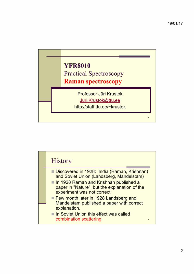
YFR8010 Practical Spectroscopy Raman spectroscopy
Professor Jüri Krustok [email protected]
http://staff.ttu.ee/~krustok
3
History n Discovered in 1928: India (Raman, Krishnan)
and Soviet Union (Landsberg, Mandelstam) n In 1928 Raman and Krishnan published a
paper in "Nature", but the explanation of the experiment was not correct.
n Few month later in 1928 Landsberg and Mandelstam published a paper with correct explanation.
n In Soviet Union this effect was called combination scattering. 4

19/01/17
3
Raman
5
Light and matter n If the light is directed on to matter we observe
absorption, reflection and scattering. n SCATTERING can be:
n Elastic (Rayleigh) → λsecondary = λprimary
n Nonelastic (Raman) → λsecondary ≠ λprimary
§ The wavelength of light changes with RAMAN scattering
6

19/01/17
4
Elastic (Rayleigh) scattering
Intensity of scattering depends on the wavelength λ of primary light and on the scattering angle Θ Blue light is scattered more than red light Blue sky- Reyleigh scattering of sunlight on molecules of air! 7
Raman vs. Rayleigh scattering Raman scattering intensity is 107 times weaker than the primary light (laser) intensity
8

19/01/17
5
Raman and FTIR (infrared spectroscopy) FTIR Raman
i. vibrational modes vibrational modes ii. change of dipole movement change in polarizability iii. Excitation of the molecule Light as an
electromagnetic field:
to higher vibrational electron state disturbing of electron cloud near the bond
δ- 2δ+ δ-
9
Physics of Raman effect n Raman spectra show very weak peaks with
frequency ω and this frequency is a combination of primary light frequency ω0 and the frequency of vibrational states of molecules (or vibrational modes of crystals) ωi.
iωωω ±= 010

19/01/17
6
Laser photon is absorbed
Excited electron levels
A
A
Virtual levels
Raman theory
11
Rayleigh scattering energy does not change!! hνin = hνout
A Raman scattering energy changes!! hνin <> hνout
Raman theory
12
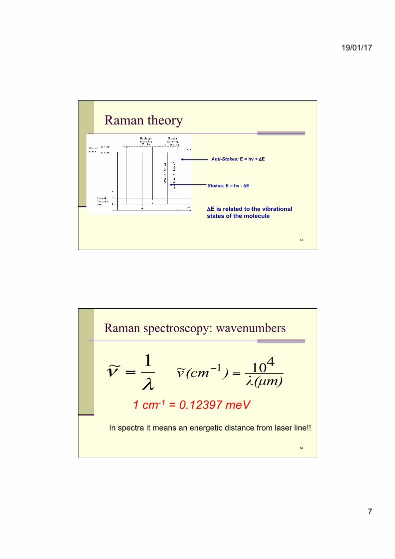
19/01/17
7
Anti-Stokes: E = hν + ΔE
Stokes: E = hν - ΔE
Raman theory
ΔE is related to the vibrational states of the molecule
13
Raman spectroscopy: wavenumbers
λ(µm))(cmν410~ 1 =−
1 cm-1 = 0.12397 meV λ
ν1~ =
In spectra it means an energetic distance from laser line!!
14

19/01/17
8
Raman spectrum In typical Raman spektrum we have: 1. Rayleigh peak (ΔE=0) 2. Anti-Stokes peaks, where the energy is increased, i.e. ΔE<0 3. Stokesi peaks, where the energy is decreased, i.e. ΔE>0 In general we record Stokesi peaks
15
Molecules and crystals
n Molecules – vibrations of molecules n Crystals- Lattice vibration modes (phonons) n Lattice vibration modes depend on symmetry
of the lattice, atomic masses and bond strengths between atoms
16

19/01/17
9
Example- chalcopyrite
CuInSe2 CuInS2 CuGaSe2 and others
17
Vibrational modes in chalcopyrite n In chalcopyrite AIBIIIC2
VI crystal we have 8 atoms in unit cell. Accordingly we have 24 vibrational modes: 1A1 + 2A2 + 3B1 + 4B2 + 7E,
From them we have 22 Raman active modes: 1A1 + 3B1 + 3B2(LO) + 3B2(TO) + 6E(LO) + 6E(TO).
n A1 always dominates spectra, because it is related to
anion movement only n B1 mode is related to cation movement and B2 and E
modes are related to movement of all atoms. 18

19/01/17
10
A1 mode in chalcopyrite
The most intensive peak in Raman spectra
19
A1 peaks in chalcopyrites
20

19/01/17
11
Raman spectra of CuInS(Se)2
21
The shape of Raman peaks
Gauss shape
Lorenz shape
22

19/01/17
12
Raman spectra Ramani peaks are very
close to the laser line n The separation of peaks
is better with red laser n Intensity of Raman
peaks is proportional to [1/λlaser]4
n blue laser gives better signal!
400 Wavelength
0 10 20 30 40 50 60
Inte
nsity
B
LUE
lase
r
GR
N la
ser
RE
D
lase
r
Fluorescence
Raman shift
Fluorescence kills a weak Raman signal 23
Micro-Raman spectrometer
Laser
CCD Detector
Sample
Obj Lens
Notch Filter
24
19/01/17
13
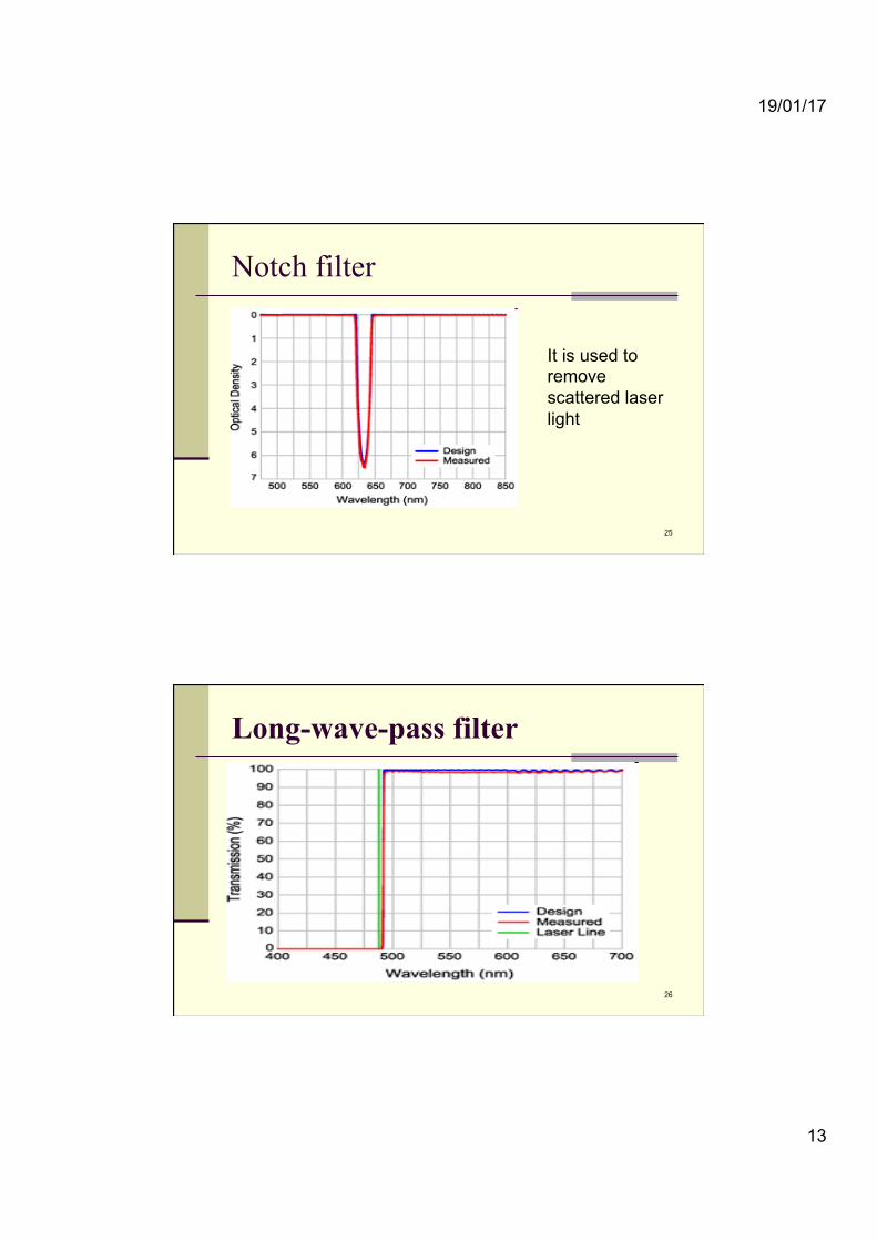
Notch filter
It is used to remove scattered laser light
25
Long-wave-pass filter
26
19/01/17
14
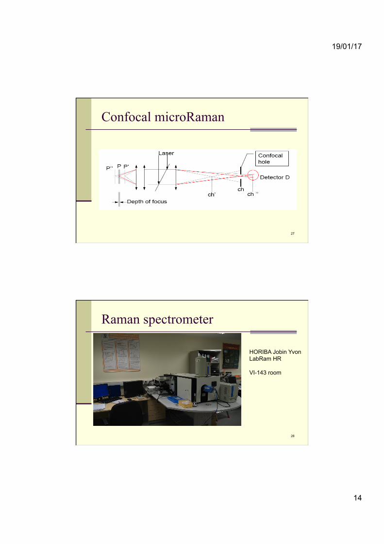
Confocal microRaman
27
Raman spectrometer
HORIBA Jobin Yvon LabRam HR VI-143 room
28

19/01/17
15
Raman spectrometer (from behind)
29
Scanning Raman
Micro scan from the surface of unknown pill 4 different peaks- 4 different colors
30
19/01/17
16
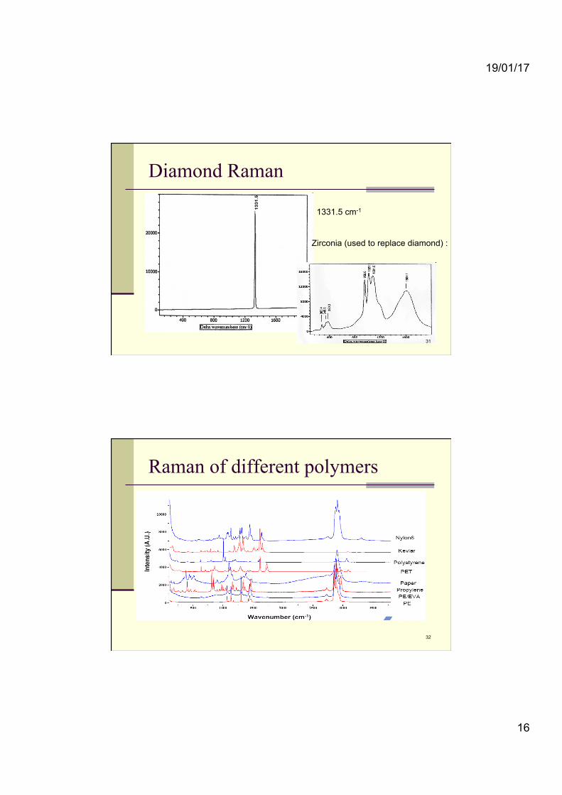
Diamond Raman
1331.5 cm-1
Zirconia (used to replace diamond) :
31
Raman of different polymers
32

19/01/17
17
Raman of human body
33
Raman of explosives
34

19/01/17
18
Fitting of Raman (and PL) spectra n Free FITYK software http://www.unipress.waw.pl/fityk/
35
Raman measurements n Measure different samples n Spectra fitting with Lorenzian function n Find Imax, Emax, W for each peak
n Memory stick !!!!
36

19/01/17
19
YFR8010 Practical Spectroscopy PHOTOLUMINESCENCE
Prof. Jüri Krustok
37
Photoluminescence in semiconductors
38

19/01/17
20
Recombination
n Radiative recombination- photoluminescence
n Non radiative recombination- DARK!
39
Equipment for photoluminescence
40

19/01/17
21
PL setup laser
41
PL measurements
Detectors: Photomultiplier tubes (PMT) :
FEU-79 (visible range)
R632- red and near infrared range
Semiconductor detectors:
Si- Visible and near infrared range (~1000nm)
InGaAs- near infrared range (~1700 nm)
PbS- infrared (~3000 nm) 42

19/01/17
22
PL measurement software in TUT- LabView project
43
E, eV
Eg Band-to-band
Excitons Shallow defects
Deep defects
PL bands in semiconductors:
44

19/01/17
23
Photoluminescence in semiconductors
n Recombination luminescence
n Center luminescence 45
Edge emission
46

19/01/17
24
Edge emission
47
GaAs edge emission
)exp()(~)( 2/1
kTEh
EhAhI gg
−−−
ννν
48

19/01/17
25
Edge emission is used in: n LED (Light emitting diode) n Semiconductor lasers
49
Excitons
E (eV) Eg
FE
DX
AX
~meV
Exciton: electron and hole pair 50
19/01/17
26
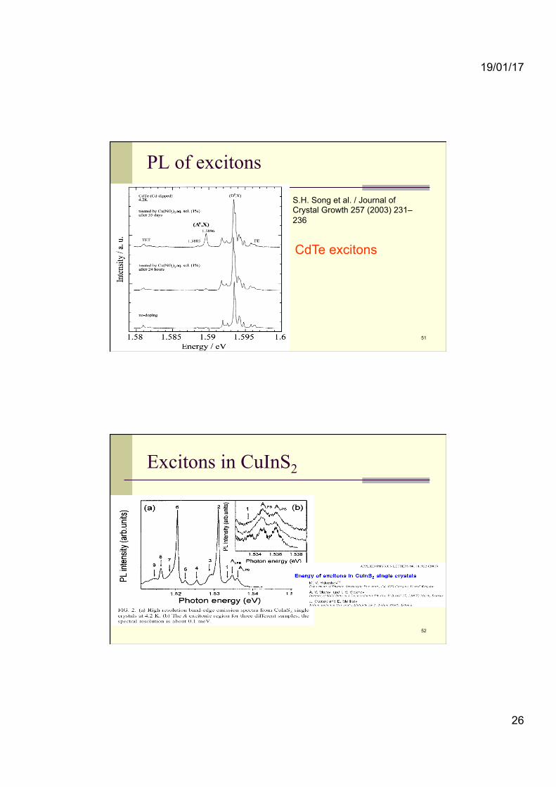
PL of excitons
S.H. Song et al. / Journal of Crystal Growth 257 (2003) 231–236
CdTe excitons
51
Excitons in CuInS2
52

19/01/17
27
Photoluminescence of donor-acceptor pairs
53
Photoluminescence of donor-acceptor pairs
n Probability of electron (on the donor defect) and hole (on the acceptor defect) recombination: WDA=Wo exp(-2R/ao)
n The PL energy of each DA pair depends on the distance between donor and acceptor R:
n In case of shallow levels we have a distribution of pairs:
ReEEERh ADgDA ε
ν2
)()( ++−=
)34exp(4)( 34 RNRNNRN DADDAπ
π −=54

19/01/17
28
Photoluminescence of donor-acceptor pairs
classic work! DAP in GaP Phys. Rev. 133, 1964, p. A269
55
Photoluminescence of donor-acceptor pairs
DAP in GaP 56

19/01/17
29
t-shift GaN MRS Internet J. Nitride Semicond. Res. 6, 12(2001).
Photoluminescence of donor-acceptor pairs
R increases W decreases t increases Emax decreases Closest pairs will recombine FASTER 57
j-shift Phys. Rev. B, 6, 1972, 3072
Photoluminescence of donor-acceptor pairs
R increases W decreases Ilaser increases Emax increases The recombination of DA pairs having larger distance will start to saturate, because the recombination probability W is small
58

19/01/17
30
Deep donor-deep acceptor pairs -> DD-DA pairs.
n DD-DA can be found in different materials. n Only closest pairs can excist between these deep
defects, because of overlap of wave-functions. n It is possible to find an energy difference between
closest pairs:
⎟⎟⎠
⎞⎜⎜⎝
⎛−=Δ
nmmn rr
eE 112
ε59
DD-DA pairs
D1 D2 W
ED0
EA0
c-band
v-band
as grown compensated
D1
D2
r1r2
r∞
60

19/01/17
31
0.6 0.8 1.0 1.2
D6D1
CuInS2
E (eV)
D6 D1AgInS2
PL i
nten
sity (
a.u.)
D6 D1
CuGaSe2
D6
D1
CuIn0.5
Ga0.5
Se2
DD-DA pairs in different ternaries. Theoretical positions are marked with vertical lines
DD-DA pairs
61
0.50 0.55 0.60 0.650
1
2
3
4
5
hω1
hω2
T=8K
CuInS2
a)
PL in
tens
ity (a
. u.)
E (eV)
0.620 0.625 0.630
D50
D40
b)
DD-DA pairs can also bound excitons: Deep excitons in CuInS2.
DD-DA pairs
62
19/01/17
32
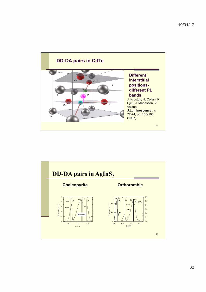
DD-DA pairs in CdTe
Different interstitial positions- different PL bands
J. Krustok, H. Collan, K. Hjelt, J. Mädasson, V. Valdna. J.Luminescence , v. 72-74, pp. 103-105 (1997).
63
0.8 1.0 1.20
1
2
3
4
5
c-AgInS2
T=8K
D6
D5D4
D3 D2D1
PL in
tens
ity (a
. u.)
E (eV)
0.6 0.8 1.0 1.20
20
40T=8K
o-AgInS2
D6 D4D5 D3 D2 D1
PL in
tens
ity (a
. u.)
E (eV)
0.0
0.1
0.2
0.3
0.4
0.5
0.6
DD-DA pairs in AgInS2
Chalcopyrite Orthorombic
64

19/01/17
33
ET
PL
Thermally liberated holes
Temperature quenching of PL
0 20 40 60 80 100 120 140-5
-4
-3
-2
-1
0
1
2
Fitting Experiment
ln (I)
1000/T (1/K)
ET =114 ± 6 meV
65
Temperature quenching of PL
q THEORY:
q J. Krustok, H. Collan, and K. Hjelt. J. Appl. Phys. v. 81, N 3, pp. 1442-1445 (1997) .
( )( )kTETT
ITIT /exp1 2
3
223
1
0
−++=
ϕϕ
66

19/01/17
34
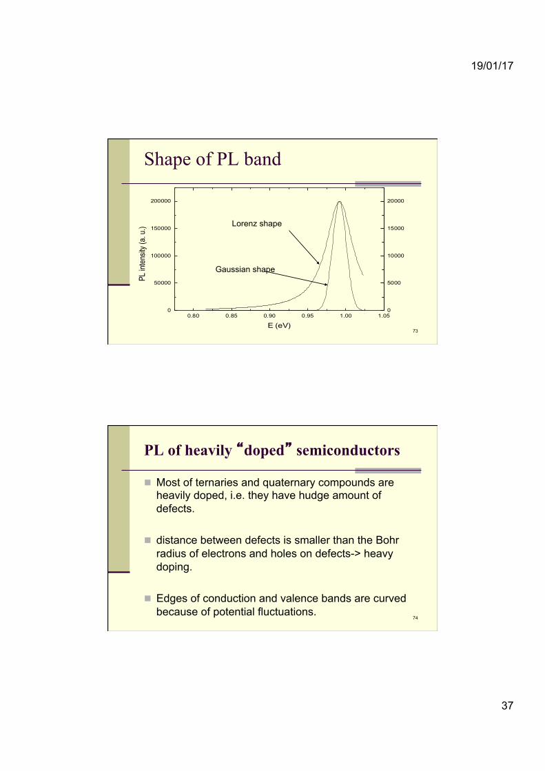
Shape of PL band
n Theory – Pekar, Huang, Rhys, jt. n The shape is not easy to calculate n Simplifications:
n T=0 n only one phonon is present and not the phonon
spectrum
Then in is possible to find transition probability from each energy level of excited state to each energy level of ground state- all these probabilities follow Poisson distribution
67
Poisson distribution !)exp()(
rrP
r µµ −=
68

19/01/17
35
Shape of PL band
n The theoretical shape of PL band is:
∑ −−−
=m
m
EmEmSSIEI )(
!)exp()( 00 ωδ !
The shape of each m-th small PL band depends mainly on interactions with acoustic phonons
69
Shape of PL band
0.00
10.00
20.00
30.00
40.00
50.00
60.00
70.00
80.00
90.00
100.00
0.85 0.90 0.95 1.00 1.05
IntF(x)
∑ −−−
=m
m
EmEmSSIEI )(
!)exp()( 00 ωδ !
E0 m=0
m=1
m=2
phonon energy
Phonon replicas having Gaussian shape
0-phonon peak
PEKARIAN
S=0.47
70

19/01/17
36
0.50 0.55 0.60 0.650
1
2
3
4
5
hω1
hω2
T=8K
CuInS2
a)
PL in
tensit
y (a.
u.)
E (eV)
0.620 0.625 0.630
D50
D40
b)
Shape of PL band
PL band in CuInS2
two phonons can be seen
71
Shape of PL band
( )⎥⎦
⎤⎢⎣
⎡ −−= 2
2max
02ln4exp)(WEEIEI
Gaussian shape:
( )⎥⎦
⎤⎢⎣
⎡ −−−= 2
20
0 )(2ln82ln4exp)(
ωω
!!
SSEEIEI
If in Pekarian S -> ∞, then we also will have a pure Gaussian shape:
72
19/01/17
37
0.80 0.85 0.90 0.95 1.00 1.050
50000
100000
150000
200000
PL in
tens
ity (a
. u.)
E (eV)
0
5000
10000
15000
20000
Shape of PL band
Lorenz shape
Gaussian shape
73
PL of heavily “doped” semiconductors
n Most of ternaries and quaternary compounds are heavily doped, i.e. they have hudge amount of defects.
n distance between defects is smaller than the Bohr radius of electrons and holes on defects-> heavy doping.
n Edges of conduction and valence bands are curved because of potential fluctuations.
74

19/01/17
38
1.05 1.10 1.15 1.20 1.25 1.30
0.0
0.2
0.4
0.6
0.8
1.0T=12.5K
PL in
tensit
y
E, eV
• J. Krustok, H. Collan, M.Yakushev, K. Hjelt. Therole of spatial potentialfluctuations in the shape ofthe PL bands of multinarysemiconductor compounds.Physica Scripta , T79, pp.179-182 (1999).
PL of heavily “doped” semiconductors
Typical PL spectrum in CuInGaSe2
75
Theory of heavily doped materials
Fn
Eg
ε
BBBT
ρc
ρv
Ec
Ev
Theory: Shklovskii, Efros Levaniuk, Osipov
76

19/01/17
39
1.1 1.2 1.3 1.40
1
2
3
4
5
240 K210 K
190 K175 K160 K145 K130 K120 K110 K95 K
80 K70 K60 K50 K40 K30 K20 K15 K12.5 K
PL in
tensit
y (a.
u.)
E (eV )
BB-band
BT-band
• J. Krustok, H. Collan, M.Yakushev, K. Hjelt. Therole of spatial potentialfluctuations in the shape ofthe PL bands of multinarysemiconductor compounds.Physica Scripta , T79, pp.179-182 (1999).
Edge emission of CuInGaSe2
BB and BT bands
77
Temperature dependence of BB and BT bands
0 50 100 150 200 2501.21
1.22
1.23
1.24
1.29
1.30
1.31
T2 = 175K
hνmax~ 2.1kT
BT- band
BB- band
T1=96K
hνmax~ - 4.4kT
hνm
ax (
eV)
T (K)
• J. Krustok, J. Raudoja, M.Yakushev, R. D.Pilkington, and H. Collan.phys. stat. sol. (a) v. 173,No 2, pp. 483-490 (1999).• J. Krustok, H. Collan, M.Yakushev, K. Hjelt.Physica Scripta , T79,pp. 179-182 (1999).
78

19/01/17
40
PL of heavily “doped” semiconductors
79
PL measurements n Measure PL spectra n Spectra fitting with Gaussian function n Find Imax, Emax and W for each PL band
80

19/01/17
41
YFR8010 Practical Spectroscopy Spectral Response of Solar Cells
Professor Jüri Krustok [email protected]
http://staff.ttu.ee/~krustok
81
I-V Curve of Solar Cell
82

19/01/17
42
Spectral Response
ideal solar cell
Lost current
83
Spectral Response- theory
2. Experimental
CZTSmonograinswere synthesized from binaries and elemental S inmolten flux by isothermal recrystallization process. The details of themonograin growth technology can be found elsewhere [18]. MGL solarcells with structure: graphite/MGL/CdS/ZnO/glass, were made frompowder crystals with a diameter of 56–63 μm as selected by sieving.The analysis area of the solar cell is determined by the back contactarea which is typically about 0.04 cm2. More details about the solarcell preparation can be found in [19].
For the temperature dependent J–V and EQE measurements solarcells were mounted in a closed cycle He cryostat. J–V measurementswere done by decreasing the temperature while EQE measurementswere done by increasing the temperature in the range T = 10–300 K.For EQE measurements the generated photocurrent was detected at0 V bias voltage. 250W standard halogen lampwith calibrated intensity(100 mW cm−2) was used as a light source and spectrally neutral netfilters for intensity dependence.
3. Results and discussion
Room temperature J–V characteristics of a studied CZTS-based MGLsolar cell showed the following properties: open-circuit voltage Voc =709 mV, short-circuit current density Jsc = 13.8 mA/cm2, fill factorFF = 61.4%, and efficiency η = 6.0%. Due to the peculiarity of the MGLsolar cell structure, the active area where the photocurrent is actuallyproduced is smaller than the analysis area. The active area is estimatedto be 75% of the back contact area after excluding the area of the bindermaterial between the absorber material powder crystals. After suchconsideration the current density per absorber material active area isestimated to be Jscabs. = 18.4 mA/cm2 and the efficiency is estimated tobe ηabs = 8.0%. In spite of that, solar cell parameters are still limiteddue to recombination and parasitic losses. The series resistances obtain-ed from the light and the dark J–V curves determined at room temper-ature by the process described by Hegedus and Shafarman [20] arerather high, Rslight = 3.6 Ω cm2 and Rsdark = 4.5 Ω cm2, accordingly.
The thermal behavior of the Voc under different light intensities isshown in Fig. 1. It is known [21] that the temperature dependence ofVoc near room temperature can be presented as
VOC ¼ EAq−nkT
qln
I00IL
! "; ð1Þ
where EA, n, k, I00, and IL are the activation energy, diode ideality factor,Boltzmann constant, reverse saturation current prefactor, and the pho-tocurrent, respectively. In general, the activation energy EA and also I00depend mainly on the dominating recombination mechanism in the
solar cell. In case of bulk recombination EA≈ Eg, where Eg is the bandgapenergy of the absorber material. The bandgap energy of CZTS slightlydepends on the type of crystal structure [12], but is usually higherthan 1.5 eV. In our sample EA ≈ 1.26 eV was determined from the Voc
(T) plot (see Fig. 1). In general, according to the theory [22] in case ofEA b Eg, the interface recombination is a dominating recombination.
The temperature dependence of the series resistance Rs found usingFig. 2 is shown in Fig. 3a where three different regions can be distin-guished. At temperatures T N 90 K (region I) Rs decreases with increas-ing temperature indicating the thermal activation of carriers [23]. Inthis region, the Rs can be presented as:
RS ¼ RS0 exp EA=kTð Þ ð2Þ
where the exponential prefactor RS0 contains all parameters that are in-dependent or weekly dependent on temperature. Using Eq. (2) the acti-vation energies EA, d=87± 3meV and EA, l=43± 1meV for dark andlight curves were found, respectively. These activation energies are inthe same range as found in [6,8,24]. At intermediate temperatures(T=90–40K, region II), the dependence of the series resistance on tem-perature changes and a typical Mott's variable-range hopping (VRH)conduction starts to dominate [25]. This type of behavior is expectedin all heavily dopedmaterialswhere spatial potentialfluctuations createdeep potential wells for holes [6,26,27]. At the same time, we also ex-pect the increasing role of bulk recombination in this temperature re-gion and therefore the VRH model is not completely valid here. Atabout T=40 K, a rapid change of Rs can be seen. In low temperature re-gion (T b 40 K, region III), Rs drops downmore than one order of magni-tude and remains almost constant down to the lowest measuredtemperature. At these very low temperatures, generated holes are notable to tunnel through the potential barrier into the interface region be-tween CZTS and CdS and therefore the interface recombination ratemust be very low.
Quantum efficiency measurement is a well-known method to de-scribe optical and electronic losses in solar cell devices. From the low-energy side of the EQE curve i.e. near the bandgap energy E≈ Eg, the ef-fective bandgap energy Eg⁎ can be determined [17] by using an approx-imation proposed by Klenk and Schock [28]:
EQE≈ KαLeff ≈ A E−E$g# $1=2
=E ð3Þ
where constant A includes all energy independent parameters,Leff = w + Ld is the effective diffusion length of minority carriers,Ld is their diffusion length in the absorber material, w is the widthof the depletion region, and α is the absorption coefficient of the ab-sorber material. The constant K is unity in absolute measurements.Consequently, the Eg⁎ value can be determined from a plot of
Fig. 1. Temperature dependence of Voc measured at different light intensities. Fig. 2. Temperature dependence of dark J–V curves.
163M. Danilson et al. / Thin Solid Films 582 (2015) 162–165
EXTERNAL QUANTUM EFFICIENCY
84

19/01/17
43
Fiding Eg
85
Finding Eg
2. Experimental
CZTSmonograinswere synthesized from binaries and elemental S inmolten flux by isothermal recrystallization process. The details of themonograin growth technology can be found elsewhere [18]. MGL solarcells with structure: graphite/MGL/CdS/ZnO/glass, were made frompowder crystals with a diameter of 56–63 μm as selected by sieving.The analysis area of the solar cell is determined by the back contactarea which is typically about 0.04 cm2. More details about the solarcell preparation can be found in [19].
For the temperature dependent J–V and EQE measurements solarcells were mounted in a closed cycle He cryostat. J–V measurementswere done by decreasing the temperature while EQE measurementswere done by increasing the temperature in the range T = 10–300 K.For EQE measurements the generated photocurrent was detected at0 V bias voltage. 250W standard halogen lampwith calibrated intensity(100 mW cm−2) was used as a light source and spectrally neutral netfilters for intensity dependence.
3. Results and discussion
Room temperature J–V characteristics of a studied CZTS-based MGLsolar cell showed the following properties: open-circuit voltage Voc =709 mV, short-circuit current density Jsc = 13.8 mA/cm2, fill factorFF = 61.4%, and efficiency η = 6.0%. Due to the peculiarity of the MGLsolar cell structure, the active area where the photocurrent is actuallyproduced is smaller than the analysis area. The active area is estimatedto be 75% of the back contact area after excluding the area of the bindermaterial between the absorber material powder crystals. After suchconsideration the current density per absorber material active area isestimated to be Jscabs. = 18.4 mA/cm2 and the efficiency is estimated tobe ηabs = 8.0%. In spite of that, solar cell parameters are still limiteddue to recombination and parasitic losses. The series resistances obtain-ed from the light and the dark J–V curves determined at room temper-ature by the process described by Hegedus and Shafarman [20] arerather high, Rslight = 3.6 Ω cm2 and Rsdark = 4.5 Ω cm2, accordingly.
The thermal behavior of the Voc under different light intensities isshown in Fig. 1. It is known [21] that the temperature dependence ofVoc near room temperature can be presented as
VOC ¼ EAq−nkT
qln
I00IL
! "; ð1Þ
where EA, n, k, I00, and IL are the activation energy, diode ideality factor,Boltzmann constant, reverse saturation current prefactor, and the pho-tocurrent, respectively. In general, the activation energy EA and also I00depend mainly on the dominating recombination mechanism in the
solar cell. In case of bulk recombination EA≈ Eg, where Eg is the bandgapenergy of the absorber material. The bandgap energy of CZTS slightlydepends on the type of crystal structure [12], but is usually higherthan 1.5 eV. In our sample EA ≈ 1.26 eV was determined from the Voc
(T) plot (see Fig. 1). In general, according to the theory [22] in case ofEA b Eg, the interface recombination is a dominating recombination.
The temperature dependence of the series resistance Rs found usingFig. 2 is shown in Fig. 3a where three different regions can be distin-guished. At temperatures T N 90 K (region I) Rs decreases with increas-ing temperature indicating the thermal activation of carriers [23]. Inthis region, the Rs can be presented as:
RS ¼ RS0 exp EA=kTð Þ ð2Þ
where the exponential prefactor RS0 contains all parameters that are in-dependent or weekly dependent on temperature. Using Eq. (2) the acti-vation energies EA, d=87± 3meV and EA, l=43± 1meV for dark andlight curves were found, respectively. These activation energies are inthe same range as found in [6,8,24]. At intermediate temperatures(T=90–40K, region II), the dependence of the series resistance on tem-perature changes and a typical Mott's variable-range hopping (VRH)conduction starts to dominate [25]. This type of behavior is expectedin all heavily dopedmaterialswhere spatial potentialfluctuations createdeep potential wells for holes [6,26,27]. At the same time, we also ex-pect the increasing role of bulk recombination in this temperature re-gion and therefore the VRH model is not completely valid here. Atabout T=40 K, a rapid change of Rs can be seen. In low temperature re-gion (T b 40 K, region III), Rs drops downmore than one order of magni-tude and remains almost constant down to the lowest measuredtemperature. At these very low temperatures, generated holes are notable to tunnel through the potential barrier into the interface region be-tween CZTS and CdS and therefore the interface recombination ratemust be very low.
Quantum efficiency measurement is a well-known method to de-scribe optical and electronic losses in solar cell devices. From the low-energy side of the EQE curve i.e. near the bandgap energy E≈ Eg, the ef-fective bandgap energy Eg⁎ can be determined [17] by using an approx-imation proposed by Klenk and Schock [28]:
EQE≈ KαLeff ≈ A E−E$g# $1=2
=E ð3Þ
where constant A includes all energy independent parameters,Leff = w + Ld is the effective diffusion length of minority carriers,Ld is their diffusion length in the absorber material, w is the widthof the depletion region, and α is the absorption coefficient of the ab-sorber material. The constant K is unity in absolute measurements.Consequently, the Eg⁎ value can be determined from a plot of
Fig. 1. Temperature dependence of Voc measured at different light intensities. Fig. 2. Temperature dependence of dark J–V curves.
163M. Danilson et al. / Thin Solid Films 582 (2015) 162–165
86

19/01/17
44
Finding Eg
1,25 1,30 1,35 1,40 1,45 1,50 1,55 1,600,0
0,3
0,6
0,9
1,2
1,5
1,8
2,1
2,4
2,7
(hν*
EQE)
2 (arb
.unit
s)
E(eV)
SnST=300K
Eg=(1,298±0,005) eV
Eg=(1,411±0,008) eV
87
What to do? n Measure EQE (E) spectrum for solar cell n Draw (EQE*E)2 vs E curves
n Calculate Eg
88

19/01/17
45
Meeting point U06 first floor end of the building room 156 Phone: +372 5236945
89


![Analytical Methods Diffusion NMR Spectroscopy in ...NMR methods was realised in the early days of NMR spectroscopy.[4] The most practical pulse sequence for meas-uring diffusion coefficients](https://static.fdocuments.in/doc/165x107/5e8766a7c364ec7447604f65/analytical-methods-diffusion-nmr-spectroscopy-in-nmr-methods-was-realised-in.jpg)