Yasser F. O. Mohammad 2010.2
25
Yasser F. O. Mohammad Yasser F. O. Mohammad 2010.2.21
Transcript of Yasser F. O. Mohammad 2010.2

Yasser F. O. MohammadYasser F. O. Mohammad
2010.2.21
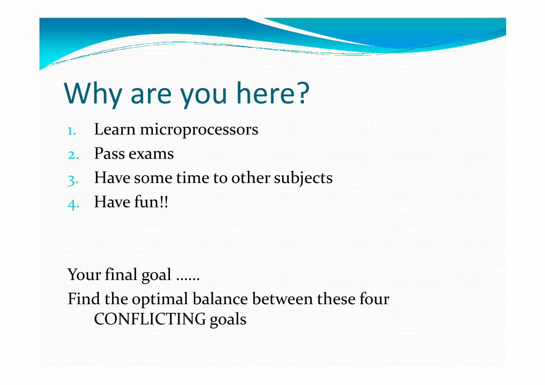
Why are you here?1. Learn microprocessors
2. Pass exams
3. Have some time to other subjects
4. Have fun!!4. Have fun!!
Your final goal ……
Find the optimal balance between these four CONFLICTING goals

Teaching Team� Instructor: Yasser F. O. Mohammad
� Computers and Systems section (Intelligent Robotics)� Email: [email protected]� Web: http://www.ii.ist.i.kyoto-u.ac.jp/~yasser
� TA: Eng. Islam
� Course Website:� http://www.ii.ist.i.kyoto-u.ac.jp/~yasser/courses/Micro3CS/
� Google Group:� May be

Course Syllabus� Introduction � Basics of 80x86 architecture (IA32)� Addressing Modes� Assembly
� Using the assemblerData movement� Data movement
� Arithmetic and Logic� Program control� Using assembly with C++� Basic system calls� Computer based Control using Assembly
� Interrupts� Basic I/O interfacing� SSE, SIMD, MMX etc� Advanced IA32 topics
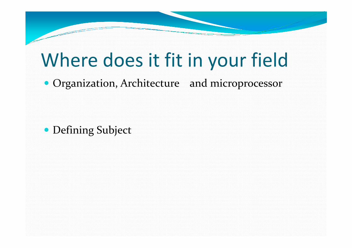
Where does it fit in your field� Organization, Architecture and microprocessor
Defining Subject� Defining Subject

Course Philosophy� Maximize practical engineering sense
� Maximize field exposure
� Learn 8x86 in order to understand othermicroprocessors as well.
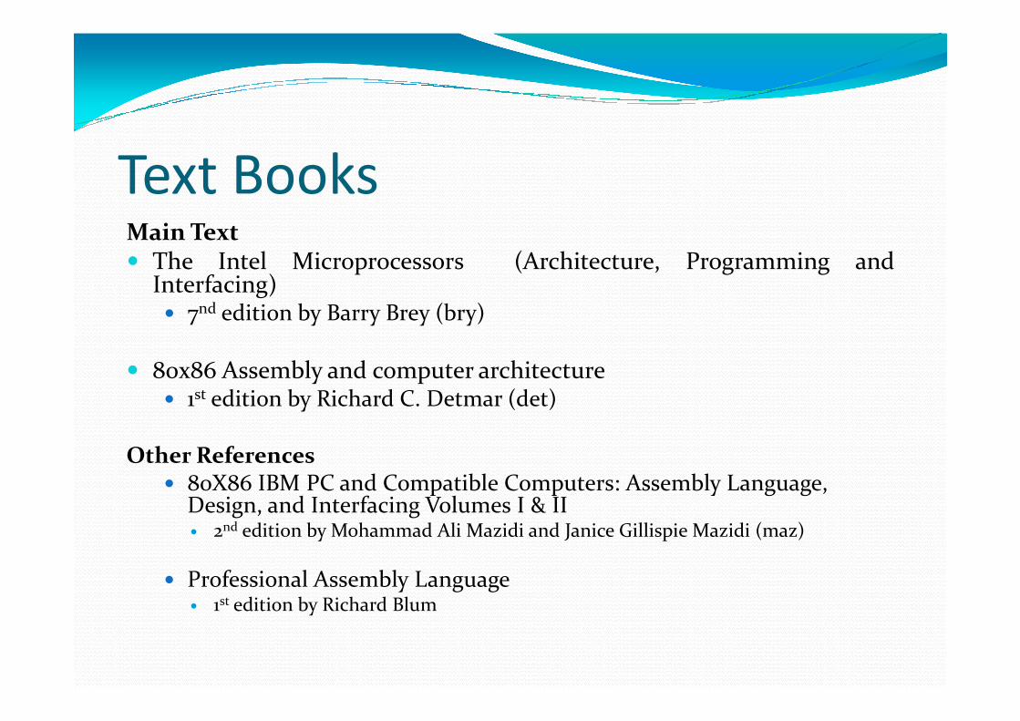
Text BooksMain Text� The Intel Microprocessors (Architecture, Programming and
Interfacing)� 7nd edition by Barry Brey (bry)
� 80x86 Assembly and computer architecture� 80x86 Assembly and computer architecture� 1st edition by Richard C. Detmar (det)
Other References� 80X86 IBM PC and Compatible Computers: Assembly Language,
Design, and Interfacing Volumes I & II� 2nd edition by Mohammad Ali Mazidi and Janice Gillispie Mazidi (maz)
� Professional Assembly Language � 1st edition by Richard Blum

Course Content (tentative)Item Source
Introduction to microprocessors and 8x86 Brey ch 1
80x86 basic internal architecture Brey ch 2
Addressing modes Brey ch 3
Elements of assembly language Det ch 3
Subject to modification any time during the semester
Elements of assembly language Det ch 3
Basic instructions Det ch 4
Branching and Looping Det ch 5
Procedures Det ch 6
String Operations Det ch 7
Bit Manipulation Det ch 8
Assembly process Det ch 9
Floating Point Arithmetic Det ch 10
Decimal Arithmetic Det ch 11
Input/Output Det ch 12

x86 Architecture (IA32)� Basic Architecture unchanged since 1978 (8086)
� CISC Architecture
� 8 General Purpose Registers
� EAX, EBX, ECX, EDX, EBP, ESP, ESI, EDI� EAX, EBX, ECX, EDX, EBP, ESP, ESI, EDI
� 6 segment registers, processor status register, and an instruction pointer
� Instruction set:� One operand can be in memory
� Variable instruction size (1 - 13 bytes)
� Memory segmentation

Ancient History� 4004:
� 4-bit microprocessor.� 4KB main memory.� 45 instructions.� PMOS technology.� 50 KIPS� 50 KIPS
� 8008: (1971)� 8-bit version of 4004.� 16KB main memory.� 48 instructions.� NMOS technology.
� 8080: (1973)� 8-bit microprocessor.� 64KB main memory.� 2 microseconds clock cycle time; 500,000 instructions/sec.� 10X faster than 8008.

Very Old History� 8085: (1977)
� 8-bit microprocessor - upgraded version of the 8080.� 64KB main memory.� 1.3 microseconds clock cycle time; 769,230 instructions/sec.� 246 instructions.� Intel sold 100 million copies of this 8-bit microprocessor.� Intel sold 100 million copies of this 8-bit microprocessor.
� 8086: (1978) 8088 (1979)� 16-bit microprocessor.� 1MB main memory.� 2.5 MIPS (400 ns).� 4- or 6-byte instruction cache.� Other improvements included more registers and additional instructions.
� 80286: (1983)� 16-bit microprocessor very similar in instruction set to the 8086.� 16MB main memory.� 4.0 MIPS (250 ns/8MHz).

Old History� 80386: (1986)
� 32-bit microprocessor.� 4GB main memory.� 12-33MHz.� Memory management unit added.� Variations: DX, EX, SL, SLC (cache) and SX.� Variations: DX, EX, SL, SLC (cache) and SX.
� 80386SX: 16MB through a 16-bit data bus and 24 bit address bus.
� 80486: (1989)� 32-bit microprocessor, 32-bit data bus and 32-bit address bus.� 4GB main memory.� 20-50MHz. Later at 66 and 100MHz� Incorporated an 80386-like microprocessor, 80387-like floating point
coprocessor and an 8K byte cache on one package.� About half of the instructions executed in 1 clock instead of 2 on the 386.� Variations: SX, DX2, DX4.
� DX2: Double clocked version:� 66MHz clock cycle time with memory transfers at 33MHz.

Recent History� Pentium: (1993)
� 32-bit microprocessor, 64-bit data bus and 32-bit address bus.
� 4GB main memory.� 60, 66, 90MHz.� 1-and-1/2 100MHz version.� Double clocked 120 and 133MHz
� Pentium Pro: (1995)� 32-bit microprocessor, 64-bit data
bus and 36-bit address bus.� 64GB main memory.� Starts at 150MHz.� 16KB L1 cache (split
instruction/data: 8KB each).� Double clocked 120 and 133MHz
versions.� 16KB L1 cache (split
instruction/data: 8KB each).� Memory transfers at 66MHz
(instead of 33MHz).� Dual integer processors.
� 16KB L1 cache (split instruction/data: 8KB each).
� 256KB L2 cache.� Memory transfers at 66MHz.� 3 integer processors.

Recent History Cont.
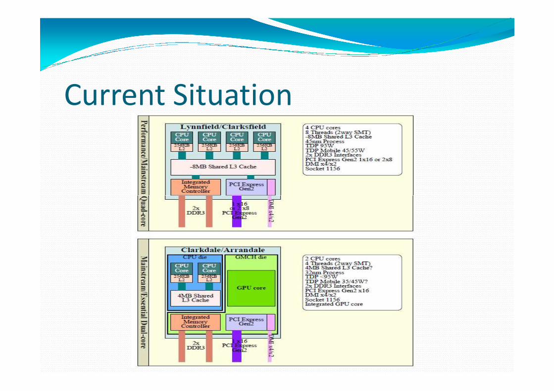
Current Situation

Future

x86 is not really x86� Basic 8086 architecture is
� difficult to speed up
� Too complex
� Current Intel microprocessors use microarchitectures
� Many Registers
� All Instructions the same size
� NetBurst, core, and atom

Memory Hierarchy
� Temporal Locality
� Spatial Locality

Cache Organization

Caches� Average memory access time = hit time + miss rate* miss penalty� Example of designing for caches
� Matlab Matrix Multiplication
� Replacement policyReplacement policy� Random, LRU, FIFO, ...
� Write policy� Write through, write back
� Unified vs. separate caches� Data and instructions together or separate?
� Exclusive vs. inclusive caches� Blocks in both L1 and L2?
� Victim caches� Stores recently evicted blocks

Instruction Level Parallism� Pipelining
� Instruction execution split into stages:
� Fetch, Decode, Execude, Memory, Write back
� Many instructions in execution at the same time� Many instructions in execution at the same time
� Just like a factory assembly line
� Superscalar
� Multiple execution units:
� 2 integer, 1 floating point, 1 logic
� SIMD (Single Instruction stream, Multible Data stream)
� Data packed into data word, one instruction produces multiple results

Intel Core Due Q6600

Intel Q6600 Cache
� Same block size in all caches (64 Bytes)
� Number of blocks� L1 ??
� L2 ??

Multicore processors� Current processors
� Intel: 4 cores
� Sun: 8 cores (UltraSPARC T2)
� Easier to increase number of cores than increase clock � Easier to increase number of cores than increase clock rate
� Software needs to be rewritten to take advantage
� Inevitable that future processors will have 10-100s of cores
� How many can be efficiently utilized?

Other Topics� Cache coherence
� Maintain same data in cache and memory in multiprocessors
� MMX, SSE, SSE2, SSE3, SSE4� MMX, SSE, SSE2, SSE3, SSE4
� Additional vectorizing instructions on 32bit floating point numbers in 128bit registers (~300 instr.)
� Hyperthreading
� Let two threads run at the same time on one processor (two sets of registers, one execution core)