Xxx Miguel Urteaga A Ph. D. thesis proposal, July 16 th, 2002.
52
xxx Miguel Urteaga A Ph. D. thesis proposal, July 16 th , 2002
-
date post
19-Dec-2015 -
Category
Documents
-
view
219 -
download
1
Transcript of Xxx Miguel Urteaga A Ph. D. thesis proposal, July 16 th, 2002.

xxx
Miguel Urteaga
A Ph. D. thesis proposal,
July 16th, 2002

Outline
• Motivation
• Research to Date
• Proposed Research
Demonstration of high-bandwidth manufacturable InP mesa-HBTs
Circuit demonstrations in technology

Motivation

Why do we want fast transistors?
Fiber Optic Communication Systems40 Gb/s, 160 Gb/s(?) long haul links
mm-Wave Wireless Transmissionhigh bandwidth communication links,atmospheric sensing, automotive radar
Military Electronics Applications> 100 GHz mixed-signal ICs for digital microwave radar

InP vs Si/SiGe HBTs
InP system has inherent material advantages over Si/SiGe
20x lower base sheet resistance, 5 x higher electron velocity, 4x higher breakdown-at same ft.
but…
Current generation production Si/SiGe HBTs are almost as fast as InP counterparts due to 5x smaller scaling
and…
SiGe HBTs offer much higher levels of integration due to underlying Si platform

Reduce vertical dimensions to decrease transit times
Reduce lateral dimensions to decrease RC time constants
Increase current density to decrease charging resistances
For a x 2 improvement of all parasitics: ft, fmax, logic speed...
base 2: 1 thinnercollector 2:1 thinner
emitter, collector junctions 4:1 narrower
current density 4:1 higher
emitter Ohmic, collector Ohmic 4:1 less resistive
Scaling Laws for HBTs

Which technology is built to scale?
E
C
B
InP mesa-HBT before passivation Cross-section of SiGe HBT
Narrow emitter: 0.18 umSelf-aligned regrown emitterHigh current density: 10 mA/um2
SiO2 trenches: small collector capacitancePlanar device : high yield
Wide emitter: >1 um Self-aligned base metal liftoff: low yieldLow current density: 2 mA/um2
Parasitic base collector capacitance under base contacts Non-planar device : low yield

• Scaling of collector-base junction
• High yield self-aligned base-emitter junction formation
• Improving emitter Ohmic contacts
• Heat flow for high current-density operation
• Device passivation for long-term reliability
• Planar process flow for high levels of integration
Key Challenges for InP HBTs

Revolutionary Approach: Si like InP HBT
N- collector
N+ subcollector
S.I. substrate
Si3
N4
intrinsic base*
regrownextrinsic base*
base contact
Si3
N4
regrown emitter *emitter contact
collector contact
*monocrystalline where grown on semiconductorpolycrystalline wheregrown on silicon nitride
Objectives: Extreme parasitic reduction: speedFully planar device: yieldSilicon-like structure: yield
Approach:
Implanted isolated subcollectorplanar surface: yield
Pedestal collector, regrown basesubmicron collector scaling: speedsmall collector junction: speedthick extrinsic base: speedplanar base-collector junction: yield
Regrown submicron emittersubmicron emitter scaling: speedno submicron etching: yieldno emitter-base liftoff: yieldlarge emitter contact: low Rex, speedlarge emitter contact: yield
Approach currently being pursued by D. Scott and N. Parthasarathy at UCSB

Evolutionary Approach: Optimized InP mesa-HBT
S.I.Substrate
N+ subcollector
N- collector
Emitter contactSi3N4 Sidewall
Base contactSiO2 sidewall
Si3N4 Sidewall
Base layer
Collector contact
Objectives: Improve speed, yield, and integration density of mesa-HBT technologyContribute processes for development of Si-like technology
Approach:
Dielectric sidewall processesself-aligned base-emitter junction with improved yield: no liftoffself-aligned definition of base Ohmic contact width for minimum Cbc
Ion implantation for base pad isolation Extrinsic Cbc reduction
Optimize Ohmic contact metallurgiesRex reduction essential for high-speed logicSkip lateral scaling generation with improved base Ohmics
Planar View
Collector contact
Emitter contact
Base contact
Ion ImplantRegion
Base contactSidewall

Research to Date

Submicron transferred-substrate HBTs with electron-beam defined emitter and collector contacts
Device measurement and characterization to 220 GHz
G-band (140-220 GHz) small-signal amplifier designs
Submicron HBTs by Substrate Transfer

Submicron HBTs have very low Ccb (< 5 fF)
Small reverse transmission characteristics and small output conductance make accurate device measurements difficult
UCSB measurement set-up allows device measurements to 220 GHz
Accurate on-wafer calibration is essential
LRL calibration with correction for Line standard complex characteristic impedance
First reported transistor measurements in 140-220 GHz band
2001 DRC, Notre Dame, IN
On-wafer Device Measurements
Transistor Embedded in LRL Test Structure
230 m 230 m
UCSB 140-220 GHz VNA Measurement Set-up

1E111E10 1E12
0
5
10
15
20
25
30
35
-5
40
Frequency, Hz
RF
Gai
ns, dB
U
MSG/MAG
h21
Emitter: 0.3 x 18 m2, Collector: 0.7 x 18.6 m2
Ic = 5 mA, Vce = 1.1 V
Transferred-Substrate Device Results
unbounded U
Recent device measurements show singularity in Unilateral Power Gain due to small negative output conductance
Not predicted from hybrid-transistor model
Cannot extrapolate fmax from device measurements
Effect may arise from second-order transport effects in collector space charge region
• Ccb cancellation
• weak IMPATT effects
“Power gain singularities in Transferred-substrate InP/InGaAs-HBTs,” submitted to IEEE TED

Applications: Wideband communication systems Atmospheric sensing Automotive radar
Utilize high available gain of submicron transferred substrate HBTs for tuned small-signal amplifiers in 140-220 GHz band
State-of-the-art InP-based HEMT Amplifiers with submicron gate lengths
3-stage amplifier with 30 dB gain at 140 GHz.
Pobanz et. al., IEEE JSSC, Vol. 34, No. 9, Sept. 1999. 3-stage amplifier with 12-15 dB gain from 160-190 GHz
Lai et. al., 2000 IEDM, San Francisco, CA. 6-stage amplifier with 20 6 dB from 150-215 GHz.
Weinreb et. al., IEEE MGWL, Vol. 9, No. 7, Sept. 1999.
Ultra-high Frequency Amplifiers (140-220 GHz)

First Generation: Single-Stage Amplifier
150 160 170 180 190 200 210140 220
-2
0
2
4
6
-4
8
Frequency, GHz
S21
, dB
150 160 170 180 190 200 210140 220
-16
-12
-8
-4
-20
0
Frequency, GHz
S11
, S22
, dB
S11
S22
S21• Measured 6.3 dB peak gain at 175 GHz
• Gain per-stage amongst highest reported
• Common-emitter design with microstrip matching network
• Device dimensions: Emitter area: 0.4 x 6 m2
Collector area: 0.7 x 6.4 m2
• Presented at 2001 GaAsIC Conference
Cell Dimensions: 690m x 350 m
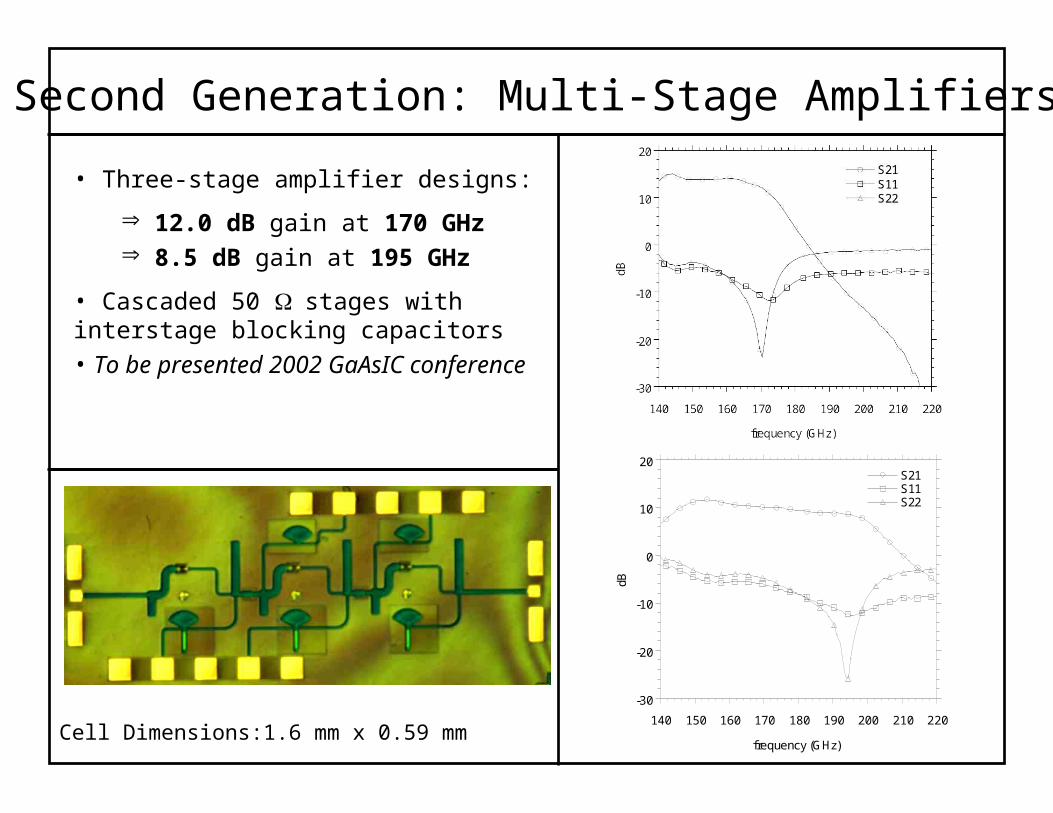
Second Generation: Multi-Stage Amplifiers
• Three-stage amplifier designs:
12.0 dB gain at 170 GHz 8.5 dB gain at 195 GHz
• Cascaded 50 stages with interstage blocking capacitors
• To be presented 2002 GaAsIC conference
Cell Dimensions:1.6 mm x 0.59 mm
-30
-20
-10
0
10
20
140 150 160 170 180 190 200 210 220
S21S11S22
dB
frequency (GHz)

Technological Implementation

Evolutionary Approach: Optimized InP mesa-HBT
S.I.Substrate
N+ subcollector
N- collector
Emitter contactSi3N4 Sidewall
Base contactSiO2 sidewall
Si3N4 Sidewall
Base layer
Collector contact
Objectives: Improve speed, yield, and integration density of mesa-HBT technologyContribute processes for development of Si-like technology
Approach:
Dielectric sidewall processesself-aligned base-emitter junction with improved yield: no liftoffself-aligned definition of base Ohmic contact width for minimum Ccb
Ion implantation for base pad isolation Extrinsic Ccb reduction
Optimize Ohmic contact metallurgiesRex reduction essential for high-speed logicSkip lateral scaling generation with improved base Ohmics
Planar View
Collector contact
Emitter contact
Base contact
Ion ImplantRegion
Base contactSidewall

• Optimized Ohmic contacts
• Self-aligned base-emitter junction formation
• Self-aligned base Ohmic width definition
• Ion Implantation for base-pad capacitance reduction
Technological Implementation

Optimized Ohmic contacts are essential for realization of high performance mesa-HBTs
Currently UCSB has the world’s best base Ohmic contacts and the world’s worst emitter Ohmic contacts
Collector contacts have not been closely examined because of Schottky collector contact TS-HBTs and the use of thick InGaAs sub-collector layers
InP HBT Ohmic Contacts

Base Ohmic Contacts
Base Ohmic process developed by M. Dahlstrom has reduced specific contact resistivity of p-type contacts to < 10-7 cm2
Improvement seen for C and Be doped samples
Transfer length of < 0.1 m allows aggressive scaling of base Ohmic contact width for reduced Ccb
Process
• UV Ozone treatment of InGaAs surface
• NH4OH oxide strip
• Pd/Ti/Pd/Au metallization
Proposed Research
• Incorporate process with new self-aligned base-emitter junction processes
• Investigate thermal stability of contacts
0
50
100
150
200
250
0 1 2 3 4 5 6 7
TLM Measurements
y = 0.6 + 38.5x R= 0.99998
Re
sist
an
ce (
Oh
m)
Spacing (m)
c< 10-7 -cm2

Emitter Ohmic Contacts
UCSB InP HBTs have large extrinsic emitter resistance Rex
Emitter resistance has contributions from vertical contact resistance, and resistances of semi-conductor layers. Approximate as Rex = e/Ae
UCSB: e= 30-50 m2
NTT: e= 7 m2
M. Ida et. al. 2001 IEDM
Variability of UCSB contacts suggest processing related problems
ee1e1ejunctee2e2e
contacteecapcapcontacteeecex
WLTWLT
WLTWLR
ρρ
ρρ
,
,,,
Proposed Research
• Optimize Ohmic contacts to n-InGaAs using refractory metallization if possible
• Determine source of high emitter resistance and optimize epi-layers and/or process to reduce Rex
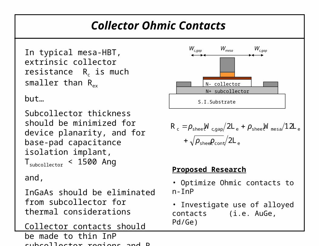
Collector Ohmic Contacts
Proposed Research
• Optimize Ohmic contacts to n-InP
• Investigate use of alloyed contacts (i.e. AuGe, Pd/Ge)
econtsheet
emesasheetegapcsheetc
L2
L12WL2WR
ρρ
ρρ ,
S.I.Substrate
N+ subcollector
N- collector
Wmesa Wc,gapWc,gapIn typical mesa-HBT, extrinsic collector resistance Rc is much smaller than Rex
but…
Subcollector thickness should be minimized for device planarity, and for base-pad capacitance isolation implant, Tsubcollector < 1500 Ang
and,
InGaAs should be eliminated from subcollector for thermal considerations
Collector contacts should be made to thin InP subcollector regions and Rc will be comparable to Rex

Base-Emitter Junction Formation
Current UCSB base-emitter junction formation relies on undercut of emitter semiconductor and self-aligned liftoff of thin base metal
Acceptable process for high-performance, small-scale integration, research fabrication
Unacceptable process for high-performance, large-scale integration, production fabrication

Base-Emitter Junction Formation
base contact
emittercontact
base contact
S.I. substrate
base
sub collector
S.I. substrate
base
sub collector
S.I. substrate
base
sub collector
emitter
S.I. substrate
base
sub collector
base contact
liftoff failure:emitter-baseshort-circuit
S.I. substrate
base
sub collector
base contact
excessiveemitter undercut
S.I. substrate
base
sub collector
S.I. substrate
base
sub collector
planarization failure: interconnect breaks
Current Base-Emitter Process Failure Mechanisms

Utilize isotropic deposition of CVD dielectric films and anisotropic etch rates of RIE to form sidewall spacers
Dielectric Sidewall Formation
Emitter Contact/ Mesa formation CVD Dielectric film
Reactive Ion Etch Sidewall Formation

• Dielectric sidewall process has been developed at UCSB
• Utilize dry-etched tungsten emitter contacts for improved emitter profile and sidewall formation
Key challenges
Etch damage to base semiconductor
Passivation of InP/InGaAs surfaces with dielectrics
Scaling sidewall thickness
Hydrogen passivation of carbon doped InGaAs base
Dielectric Sidewall Formation: Current Status
1 m Tungsten Emitter w/ 1000A SiN sidewall

Carbon is preferred to Beryllium as base dopant because of lower diffusion coefficient and higher solubility
Hydrogen passivation of Carbon acceptors in InGaAs is observed in MOCVD growth and during Methane base dry-etches
SixNy CVD deposition utilizes SiH4 carrier gas. Carbon passivation during ECR-CVD of SixNy has been reported.
Ren, F et. al. Solid-State Electronics May, 1996
Possible Solutions
• SixNy deposition on base-emitter grade
• Anneal out hydrogen; 400 C ~10 min anneal requires refractory contacts
• Use Be doped base
• GaAsSb base layer
Key Challenge: Hydrogen Passivation of C-doped InGaAs

InAlAs/GaAsSb/InP DHBTs
In52Al48As
GaAs50Sb50
InP
MOCVD of C-doped GaAsSb shows no hydrogen passivation
Initial experiments at UCSB show no passivation after SixNy deposition
High performance InP/GaAsSb/InP DHBTs have been demonstrated ft, fmax = 300 GHz
Dvorak, et. al. IEEE EDL Aug. 2001
InAlAs/GaAsSb/InP HBTs have favorable band lineup and good surface properties for BE passivation
MBE growth of p-type GaAsSb looks promising
Be : NA = 6.6E19 cm-3; = 26.6 cm2/Vs
C : NA = 4E19 cm-3; = 46 cm2/Vs
Large area DC I-V

Approaches to base-emitter junction formation with sidewall spacers
• Blanket metallization and planarization etch back
• Selective metallization of base semiconductor: CVD, or electroplating
• Self-aligned liftoff of thin base metal with sidewalls to prevent metal-to-metal short circuits
Self-aligned base-emitter junction formation

Base-emitter junction formation: Base metal liftoff
Self-aligned emitter mesa Sidewall formation Thin metal liftoff
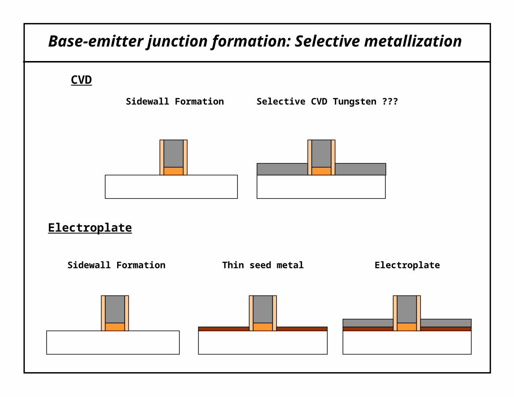
Base-emitter junction formation: Selective metallization
Sidewall Formation Selective CVD Tungsten ???
Sidewall Formation Thin seed metal Electroplate
CVD
Electroplate

Base-emitter junction formation: Planarization etchback
Sidewall Formation Blanket metallization Planarization
Etchback Metal sidewall removal Strip planarization material

Planarization etchback experiments
Similar process is incorporated in Hitachi GaAs HBT processReference
Planarization etch back experiments at UCSB were unsuccessful due to non-uniformity of RIE system
Experiments at Rockwell Science Center look better but still work to be done
Etch selectivity between planarization material and Tungsten is a key processing issue
Proposed Research
• Further experiments at RSC to determine feasibility of process
• If unsuccessful, look at alternative self-aligned processes

Base Ohmic transfer length < 0.1 m allows for aggressive scaling of base Ohmic contacts for reduced Cbc
Current self-aligned liftoff process requires accurate stepper alignment and emitter topology presents challenges for further scaling
Low yield seen for 0.3 m base Ohmic width
Utilize sidewall process for base Ohmic definition
Self-aligned base Ohmic formation

Self-aligned base Ohmic: Process Flow
Outer sidewall formation
RIE base metal
Self-aligned metallization
Self-aligned base Ohmic
Sidewall thickness determined by thickness of PECVD deposition
Repeatable definition of base Ohmic width if base metal can be selectively dry etched
Continue process with self-aligned base-mesa etch
Goal:
Repeatable, high-yield definition of < 0.3 m base metal width

Base contact pad represents considerable fraction of total extrinsic base collector capacitance
~34 % of total Ccb for current generation ECL logic transistors with 0.7 m emitter and 0.5 m base Ohmic width operating at 2.5 x 10⁵ A/cm2
Fraction of total Ccb will increase dramatically as devices are laterally scaled for reduced Ccb and vertically scaled for high current
density operation
~52 % of total Ccb, for next generation ECL logic transistors with 0.5 m emitter and 0.3 m base Ohmic width operating at 5 x 10⁵ A/cm2
Base-pad Capacitance
Planar View
Collector contact
Emitter contact
Base contact pad
Base contact

Approaches to reducing extrinsic base pad capacitance include:
• Lateral undercut of contact region for isolation
• Dielectric refill and planarization of extrinsic region
• Ion implantation of extrinsic base region
Ion Implantation of InP
Damage implants of light ions in InP tend to generate shallow level traps
Unsuitable for device isolation
Adequate for base-pad capacitance reduction
Base-pad capacitance reduction

Implant Region
base
emitter
subcollector
collector
Base-pad capacitance reduction: He+ Implant
Circuit simulations show sheet resistance > 1Msquare is adequate to provide base-pad isolation
Implant experiments with He+ into 1500 Ang. InP sub-collector show sheet resistance of ~ 10 Msquare
Projected range of He+ implant will allow implant as first processing step
Proposed Research
• Transistor fabrication with base-pad isolation implant
• Determine minimum implant to device separation
• Explore Fe implant for device isolation pending experiments by N. Parthasarathy
Implant RegionPlanar View
Cross-section

InGaAs 1E19 Si 300 Å
Grade 1E19 Si 200 Å
InAlAs 8E17 Si 300 Å
Grade 8E17 Si 233 Å
Grade 2E18 Be 67 Å
InGaAs 8E19 C 300 Å
Grade 1E16 Si 200 Å
InP 2E18 Si 1100 Å
InGaAs 1E19 Si 50 Å
Layer Structure for Advanced mesa-HBT
InAs 2E19 Si 200 Å
InGaAs 1E16 Si 200 Å
Emitter cap, InAs for improved contact resistance
Thin InAlAs emitter
GaAsSb or Be-doped if necessary
Collector setback layer
1500 Ang. total collector thickness
InP 1E19 Si 1500 Å
Thin subcollector etch stop
Subcollector; no buffer layer

Predicted Performance

State-of-the-art InP mesa-HBTs
NTT: ft = 341 GHz, fmax = 250 GHz1500 Ang. collector, high current density 8 x 10⁵ A/cm2, lateral undercut for base pad isolationM. Ida et. al. 2001 IEDM
SFU: ft = 300 GHz, fmax = 300 GHzGaAsSb base, 2000 Ang. collector, airbridge contacts for base pad isolation, lateral etch collector undercutM. Dvorak, et. al. IEEE EDL Aug. 2001
UCSB: ft = 280 GHz, fmax >450GHzGraded C-doped InGaAs base, 2000 Ang. composite collector, highly-scaled base Ohmics, no base pad isolationM. Dahlstrom, et. al. 2002 IPRM
0
5
10
15
20
25
30
1010 1011 1012
Gai
n (
dB
) H
21,
U
frequency (GHz)
ft=282 GHz
fmax
=480 GHz
UCSB record fmax mesa-HBT
Figures-of-merit do not tell the whole story

Mesa-HBTs for Digital Logic
-0.2
-0.18
-0.16
-0.14
-0.12
-0.1
-0.08
-0.06
22 22.02 22.04 22.06 22.08 22.1 22.12 22.14
87 GHz input, 43.5 GHz output
Vo
ut (
Vol
ts)
time (nsec)
Transistor figures-of-merit do not accurately predict digital logic speed
Time constants CcbVlogic/Ic and CcbRex have larger contribution to digital logic gate delays than to ft
UCSB record 87 GHz static frequency divider fabricated with ft = 200 GHz, fmax = 180 GHz device operating at Je = 2.5 x 10⁵ A/cm2
PK Sundararajan PhD thesis
Similarly, MSG/MAG is better metric for mm-wave tuned amplifier design than Unilateral power gain used to extrpolate fmax

Use HBT SPICE model to predict improvements in device performance from process enhancements
Next generation ECL transistor:
We= 0.5 m, Le= 3.0 m, Je= 5 x 10⁵ A/cm2, Tcollector= 1500 Ang, Tbase= 300 Ang
Physical parameters from current generation mesa-HBTs
Consider improvements in
• ft and fmax
• Maximum ECL static divider frequency (no layout parasitics)
• Maximum available gain at 175 GHz ( Le = 6 m)
Predicted Performance: SPICE Simulations

Predicted Performance: Rex Reduction
Base Ohmic width = 0.5 m, Standard base-pad capacitance
e (-m2) ft fmaxMax Divider
Freq. MAG @ 175 GHz
50 233 GHz 423 GHz 64 GHz 4.9 dB
40 248 GHz 434 GHz 81 GHz 5.0 dB
30 266 GHz 446 GHz 92 GHz 5.1 dB
20 287 GHz 458 GHz 102 GHz 5.3 dB
10 313 GHz 472 GHz 117 GHz 5.6 dB
5 329 GHz 478 GHz 121 GHz 5.8 dB

Predicted Performance: Self-aligned base Ohmic
e = 30 -m2, Standard base-pad capacitance
Base Ohmic Width
ft fmaxMax. Divider
Freq. MAG @ 175 GHz
0.5 m 266 GHz 446 GHz 92 GHz 5.1 dB
0.25 m 290 GHz 464 GHz 109 GHz 6.0 dB

Predicted Performance: Base-pad Isolation
e = 30 -m2, Base Ohmic width = 0.5 m
Base Pad Isolation
ft fmaxMax. Divider
Freq. MAG @ 175 GHz
No 266 GHz 446 GHz 92 GHz 5.1 dB
Yes 289 GHz 450 GHz 112 GHz 5.7 dB

Predicted Performance: All Enhancements
e = 10 -m2, Base Ohmic width = 0.25 m, Base-pad Isolation
ft fmaxMax. Divider
Freq. MAG @ 175 GHz
344 GHz 487 GHz 160 GHz 7.2 dB
8.8 dB with b_cont = 1 x 10⁻⁸-cm2

Proposed Circuit Demonstrations
Static Frequency Dividers: divide-by-two, divide-by-four
Analog Wideband Amplifiers: Cherry-Hooper
mm-Wave Tuned Amplifiers:140-220 GHz frequency band

Research Timeline
Implement process enhancements using current device mask set
Base pad isolation:

Things to do when:
SEM Rockwell experimentsMore samples for S3 processing at Rockwell: Thicker emitter, thinner base metal (how thin?)
Emitter contact experiments on remaining InGaAs waferLiterature search on N+ InGaAs contacts ---Work function stuff???? Something besides Ti
Mask set for Ion Implant of InP DHBTs for base pad reductionImplant through whole structure or just base collector?? Measure straggle on bits an pieces of He implanted structure
Layer structures from DennisInAs cap on InAlAs for Ohmic contact studiesInAlAs grade on carbon doped InGaAs. Check for H passivation maybe able to use old mattias Epi, also for implant stuff.
GaAsSb when system B comes back up!!
Order IQE epi.
Go See Val tomorrow!!!