XTP129 - ML631 U2 DDR3 MIG Design Creation - Xilinx · mig_39_u2_c3_ddr3 – For each one,...
59
© Copyright 2012 Xilinx ML631 U2 DDR3 MIG Design Creation March 2012 XTP129
Transcript of XTP129 - ML631 U2 DDR3 MIG Design Creation - Xilinx · mig_39_u2_c3_ddr3 – For each one,...

© Copyright 2012 Xilinx
ML631 U2 DDR3 MIG Design Creation
March 2012
XTP129

© Copyright 2012 Xilinx, Inc. All Rights Reserved. XILINX, the Xilinx logo, the Brand Window and other designated brands included herein are trademarks of Xilinx, Inc. All other trademarks are the property of their respective owners. NOTICE OF DISCLAIMER: The information disclosed to you hereunder (the “Information”) is provided “AS-IS” with no warranty of any kind, express or implied. Xilinx does not assume any liability arising from your use of the Information. You are responsible for obtaining any rights you may require for your use of this Information. Xilinx reserves the right to make changes, at any time, to the Information without notice and at its sole discretion. Xilinx assumes no obligation to correct any errors contained in the Information or to advise you of any corrections or updates. Xilinx expressly disclaims any liability in connection with technical support or assistance that may be provided to you in connection with the Information. XILINX MAKES NO OTHER WARRANTIES, WHETHER EXPRESS, IMPLIED, OR STATUTORY, REGARDING THE INFORMATION, INCLUDING ANY WARRANTIES OF MERCHANTABILITY, FITNESS FOR A PARTICULAR PURPOSE, OR NONINFRINGEMENT OF THIRD-PARTY RIGHTS.
Revision History
Date Version Description 03/16/12 13.4 Updated for 13.4
10/26/11 13.3 Updated for 13.3.
08/30/11 13.2 Initial version.

Overview
Virtex-6 DDR3 Memory Interface ML631 Board
– Memories on the ML631
ML631 Setup Generate MIG Example Designs Modifications to Example Designs Run MIG Example Designs Adjust Data Pattern using VIO Console References
Note: This presentation applies to the ML631

Xilinx ML631 Board
Note: Presentation applies to the ML631

Xilinx ML631 Board
U1 (1) has 9 banks of 32-bit (2 x 16) DDR3 (2)
Note: Presentation applies to the ML631
1 2

Xilinx ML631 Board
U2 (1) has 4 banks of 16-bit DDR3 (2) and 2 36-bit QDRII+ (3)
Note: Presentation applies to the ML631
1
3 2

ISE Software Requirements
Xilinx ISE 13.4 software
Note: Presentation applies to the ML631

ChipScope Pro Software Requirement
Xilinx ChipScope Pro 13.4 software
Note: Presentation applies to the ML631

Setup for the ML631 MIG Designs
Important: Set the power switch, SW1, to OFF first (1) The ML631 uses two power supplies; connect both power supplies
– Use a power strip to turn on both power supplies simultaneously
SW1 must not be turned on until after the power strip is on.
1

Setup for the ML631 MIG Designs
When powering down, turn the SW1 off, then turn off the power strip – Always follow this sequence when cycling power to the ML631
Leave the power off for now

Setup for the ML631 MIG Designs
ATX power supplies can be used in lieu of standard power supplies The +12 V on each supply must be capable of supplying 15 A

Setup for the ML631 MIG Designs
Connect a USB Type-A to Mini-B cable to the USB JTAG connector on the ML631 board – Connect this cable to your PC
Note: Presentation applies to the ML631

Generate MIG Example Design
Open the CORE Generator Start → All Programs → Xilinx ISE Design Suite 13.4 → ISE Design Tools → Tools → CORE Generator
Create a new project; select File → New Project
Note: Presentation applies to the ML631

Generate MIG Example Design
Create a project directory: C:\ml631_mig_design and save the project file
Note: Presentation applies to the ML631

Generate MIG Example Design
Select Part Set the Part (as
shipped on the ML631): – Family: Virtex6 – Device: xc6vhx565t – Package: ff1923 – Speed Grade: -2
Select Generation
Note: Presentation applies to the ML631

Generate MIG Example Design
Under Generation – Set the Design Entry
to Verilog
Click OK
Note: Presentation applies to the ML631

U2 16-bit DDR3 Example

U2 16-bit DDR3 Example
Right click on MIG Virtex6 and Spartan6, Version 3.9 – Select Customize and Generate
Note: Presentation applies to the ML631

U2 16-bit DDR3 Example
Leave this page as is – Click Next

U2 16-bit DDR3 Example
Set Component Name: – mig_39_u2_c0_ddr3 – Click Next

U2 16-bit DDR3 Example
Leave this page as is – Click Next

U2 16-bit DDR3 Example
Select Memory Type – DDR3 SDRAM – Click Next
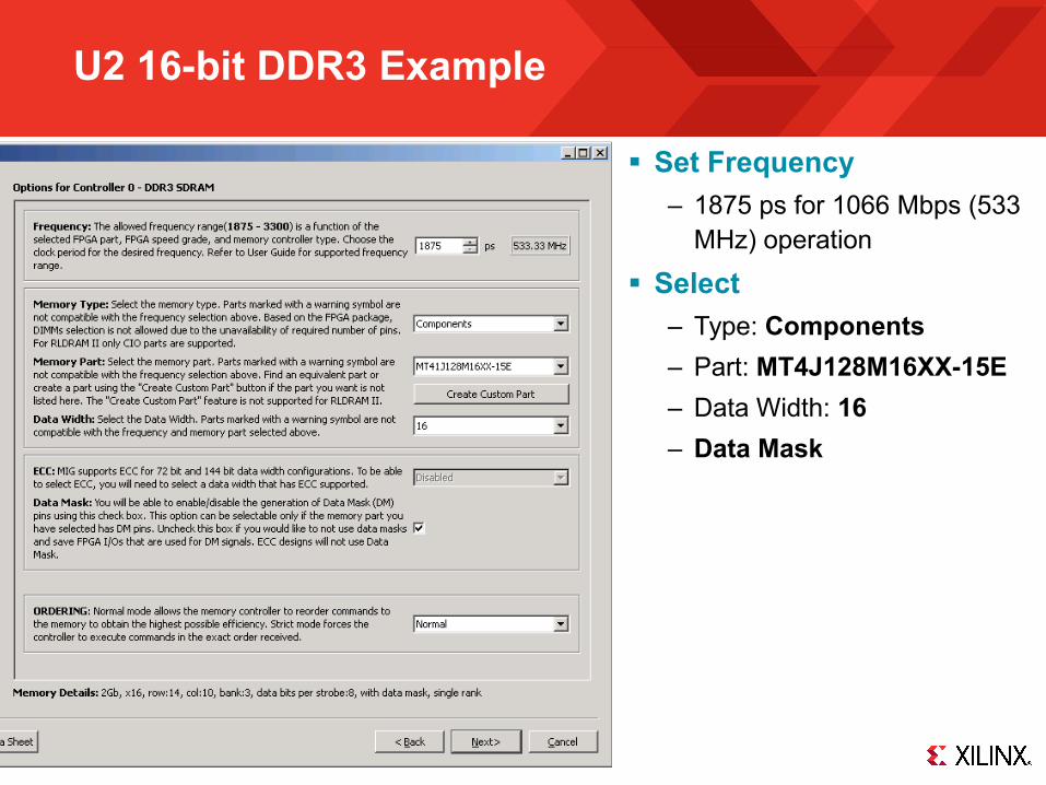
U2 16-bit DDR3 Example
Set Frequency – 1875 ps for 1066 Mbps (533
MHz) operation
Select – Type: Components – Part: MT4J128M16XX-15E – Data Width: 16 – Data Mask

U2 16-bit DDR3 Example
Leave this page as is – Click Next

U2 16-bit DDR3 Example
Select – Debug: ON – Select: Internal Vref

U2 16-bit DDR3 Example
Select New Design – Click Next

U2 16-bit DDR3 Example
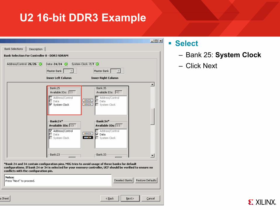
On this screen, you will select the banks as used on the ML631 U2 DDR3 interface
To start, click Deselect Banks

U2 16-bit DDR3 Example
All Banks Deselected

U2 16-bit DDR3 Example
Select – Bank 24: Address/Control

U2 16-bit DDR3 Example
Select – Bank 34: Data
U2 16-bit DDR3 Example
Select – Bank 25: System Clock – Click Next

U2 16-bit DDR3 Example
Leave this page as is – Click Next

U2 16-bit DDR3 Example
Accept Simulation license, if desired – Otherwise, Decline
license – Click Next

U2 16-bit DDR3 Example
Leave this page as is – Click Next

U2 16-bit DDR3 Example
Click Generate

U2 16-bit DDR3 Example
After the MIG core finishes generating, click Close on the Datasheet window
Note: Presentation applies to the ML631

U2 16-bit DDR3 Example
16-bit DDR3 MIG design appears in Project IP
Note: Presentation applies to the ML631

Generate Other Example Designs
Create the other DDR3 Designs – Three more 16-bit
designs: • mig_39_u2_c1_ddr3 –
mig_39_u2_c3_ddr3
– For each one, double-click on the initial version in CORE Generator, change the component name in MIG, then generate it without any changes

Modifications to Example Design
ML631 MIG Design Files (13.4 C) includes – ChipScope Project File, UCF, and Verilog Files
Modifications to RTL Files for ML631 Example Design – Changed design to support a single 200 MHz DIFF_SSTL15 clock input – Added Debug display code to drive LEDs – Added ChipScope ILA and VIO port assignments for ML631 board debug – Removed IIC Signals – sda, scl – Changed various parameter to match the ML631 board
• DIVCLK_DIVIDE = 1 (was 2) • nDQS_COLx • DQS_LOC_COLx • RST_ACT_LOW = 0 (was 1)
Note: Presentation applies to the ML631

Modifications to Example Design
Updates to UCF file specifically required for ML631 board: – Updated IO Locations to match ML631 – Remove IIC Signals – sda, scl – Merged Default two clocks into one clock for ML631 – Moved sys_reset to CPU_RESET – Edited DCI_CASCADE to match ML631 – Removed CONFIG_PROHIBIT lines – Added LOC for GPIO LED signals (1.5V bank voltage) – Added LOCs for RSYNC OSERDES and IODELAY
Note: Presentation applies to the ML631

Modifications to Example Design
Unzip the ML631 MIG Design Files (13.4 C) to the C:\ml631_mig_design directory – This adds modifications to the example design – 15 fully pre-built ML631 example designs are included in the zip file
• Use the included bitstream to run MIG with ChipScope • Run build_all.bat in <design directory>\ml631_prebuilt_example_design\ to recompile
the 15 pre-built example designs
Note: Overwrites Core Generator output files with ML631 specific files

Compile Example Design
Start a ISE Design Suite Command Prompt and enter these commands:
cd C:\ml631_mig_design\mig_39_u2_c0_ddr3\example_design\par ise_flow.bat
Note: Presentation applies to the ML631

Run U2 16-bit DDR3 Example Design
Set the power switch, SW1, to OFF (1) Turn on the power strip (with the two ML631 power supplies) Turn on the power switch (1)
1

Run U2 16-bit DDR3 Example Design
Open ChipScope Pro and select JTAG Chain -> USB Cable… (1) Verify 12 MHz operation and click OK (2)
1
2
Note: Presentation applies to the ML631

Run U2 16-bit DDR3 Example Design
Click OK (1)
1
Note: Presentation applies to the ML631

Run U2 16-bit DDR3 Example Design
Select File → Open Project… Select <Design Path>\ready_for_download\ml631_u2_c0_ddr3.cpj
Note: Presentation applies to the ML631

Run U2 16-bit DDR3 Example Design
Select Device → DEV:2 MyDevice2 (XC6VHX565T) → Configure… Select <Design Path>\ready_for_download\ml631_u2_c0_ddr3.bit
Note: Presentation applies to the ML631

Run U2 16-bit DDR3 Example Design
Click on Trigger Setup to view trigger settings The error bit value should be set to 1
Note: Presentation applies to the ML631

Run U2 16-bit DDR3 Example Design
Click on Waveform; click the Arm Trigger button (1) Detection of an error will cause ChipScope Pro to trigger
Note: Presentation applies to the ML631
1

Run U2 16-bit DDR3 Example Design
The Example Design should run error free (no trigger on error) To force a trigger, click the T! button (1)
Note: Presentation applies to the ML631
1

Adjust Data Pattern using VIO Console
Set tg_data_mode to “3” for HAMMER_DATA_MODE
Note: Presentation applies to the ML631

Adjust Data Pattern using VIO Console
Press SW15 after each change to tg_mod_en_sel or tg_data_mode
Note: Presentation applies to the ML631

Adjust Data Pattern using VIO Console
Hammer Data Mode
Note: Presentation applies to the ML631

Adjust Data Pattern using VIO Console
Set tg_data_mode to “7” for PRBS data pattern Push CPU Reset, click Arm Trigger button, click T! button
Note: Presentation applies to the ML631

Adjust Data Pattern using VIO Console
PRBS Data Mode
Note: Presentation applies to the ML631

References

References
Virtex-6 Memory – Virtex-6 FPGA Memory Interface Solutions User Guide – UG406
http://www.xilinx.com/support/documentation/ip_documentation/ug406.pdf – Virtex-6 FPGA Memory Interface Solutions – DS186
http://www.xilinx.com/support/documentation/ip_documentation/ds186.pdf – Virtex-6 FPGA Data Sheet: DC and Switching Characteristics – DS152
http://www.xilinx.com/support/documentation/data_sheets/ds152.pdf

Documentation
Documentation
Virtex-6 – Virtex-6 HXT FPGAs
http://www.xilinx.com/products/silicon-devices/fpga/virtex-6/hxt.htm
ML631 Documentation – Virtex-6 HXT FPGA Packet Processing/Traffic Management (PP/TM) Kit
http://www.xilinx.com/products/boards-and-kits/EK-V6-ML631-G.htm – ML631 Hardware User Guide
http://www.xilinx.com/support/documentation/boards_and_kits/ ug841-ml631-packet-processor-evaluation-board.pdf


![4Gb A-die DDR3 SDRAM - МТ System · DDR3 SDRAM Addressing ... 11. 4Gb DDR3 SDRAM A-die IDD Specification Table ... [ Table 1 ] Samsung 4Gb DDR3 A-die ordering information table](https://static.fdocuments.in/doc/165x107/5ad5dbf67f8b9a5c638d9a55/4gb-a-die-ddr3-sdram-sdram-addressing-11-4gb-ddr3-sdram-a-die-idd-specification.jpg)