Xilinx XC5200 Series Field Programmable Gate Arrays ... · Max Logic Gates 3,000 6,000 10,000...
73
November 5, 1998 (Version 5.2) 7-83 7 Features • Low-cost, register/latch rich, SRAM based reprogrammable architecture - 0.5μm three-layer metal CMOS process technology - 256 to 1936 logic cells (3,000 to 23,000 “gates”) - Price competitive with Gate Arrays • System Level Features - System performance beyond 50 MHz - 6 levels of interconnect hierarchy - VersaRing ™ I/O Interface for pin-locking - Dedicated carry logic for high-speed arithmetic functions - Cascade chain for wide input functions - Built-in IEEE 1149.1 JTAG boundary scan test circuitry on all I/O pins - Internal 3-state bussing capability - Four dedicated low-skew clock or signal distribution nets • Versatile I/O and Packaging - Innovative VersaRing ™ I/O interface provides a high logic cell to I/O ratio, with up to 244 I/O signals - Programmable output slew-rate control maximizes performance and reduces noise - Zero Flip-Flop hold time for input registers simplifies system timing - Independent Output Enables for external bussing - Footprint compatibility in common packages within the XC5200 Series and with the XC4000 Series - Over 150 device/package combinations, including advanced BGA, TQ, and VQ packaging available • Fully Supported by Xilinx Development System - Automatic place and route software - Wide selection of PC and Workstation platforms - Over 100 3rd-party Alliance interfaces - Supported by shrink-wrap Foundation software Description The XC5200 Field-Programmable Gate Array Family is engineered to deliver low cost. Building on experiences gained with three previous successful SRAM FPGA fami- lies, the XC5200 family brings a robust feature set to pro- grammable logic design. The VersaBlock ™ logic module, the VersaRing I/O interface, and a rich hierarchy of inter- connect resources combine to enhance design flexibility and reduce time-to-market. Complete support for the XC5200 family is delivered through the familiar Xilinx soft- ware environment. The XC5200 family is fully supported on popular workstation and PC platforms. Popular design entry methods are fully supported, including ABEL, sche- matic capture, VHDL, and Verilog HDL synthesis. Design- ers utilizing logic synthesis can use their existing tools to design with the XC5200 devices. . 0 XC5200 Series Field Programmable Gate Arrays November 5, 1998 (Version 5.2) 0 7* Product Specification R Table 1: XC5200 Field-Programmable Gate Array Family Members Device XC5202 XC5204 XC5206 XC5210 XC5215 Logic Cells 256 480 784 1,296 1,936 Max Logic Gates 3,000 6,000 10,000 16,000 23,000 Typical Gate Range 2,000 - 3,000 4,000 - 6,000 6,000 - 10,000 10,000 - 16,000 15,000 - 23,000 VersaBlock Array 8 x 8 10 x 12 14 x 14 18 x 18 22 x 22 CLBs 64 120 196 324 484 Flip-Flops 256 480 784 1,296 1,936 I/Os 84 124 148 196 244 TBUFs per Longline 10 14 16 20 24 Product Obsolete or Under Obsolescence
Transcript of Xilinx XC5200 Series Field Programmable Gate Arrays ... · Max Logic Gates 3,000 6,000 10,000...

7
Product Obsolete or Under Obsolescence
Features• Low-cost, register/latch rich, SRAM based
reprogrammable architecture- 0.5µm three-layer metal CMOS process technology- 256 to 1936 logic cells (3,000 to 23,000 “gates”)- Price competitive with Gate Arrays
• System Level Features- System performance beyond 50 MHz- 6 levels of interconnect hierarchy- VersaRing™ I/O Interface for pin-locking- Dedicated carry logic for high-speed arithmetic
functions- Cascade chain for wide input functions- Built-in IEEE 1149.1 JTAG boundary scan test
circuitry on all I/O pins- Internal 3-state bussing capability- Four dedicated low-skew clock or signal distribution
nets• Versatile I/O and Packaging
- Innovative VersaRing™ I/O interface provides a high logic cell to I/O ratio, with up to 244 I/O signals
- Programmable output slew-rate control maximizes performance and reduces noise
- Zero Flip-Flop hold time for input registers simplifies system timing
- Independent Output Enables for external bussing
- Footprint compatibility in common packages within the XC5200 Series and with the XC4000 Series
- Over 150 device/package combinations, including advanced BGA, TQ, and VQ packaging available
• Fully Supported by Xilinx Development System- Automatic place and route software- Wide selection of PC and Workstation platforms- Over 100 3rd-party Alliance interfaces- Supported by shrink-wrap Foundation software
DescriptionThe XC5200 Field-Programmable Gate Array Family isengineered to deliver low cost. Building on experiencesgained with three previous successful SRAM FPGA fami-lies, the XC5200 family brings a robust feature set to pro-grammable logic design. The VersaBlock™ logic module,the VersaRing I/O interface, and a rich hierarchy of inter-connect resources combine to enhance design flexibilityand reduce time-to-market. Complete support for theXC5200 family is delivered through the familiar Xilinx soft-ware environment. The XC5200 family is fully supported onpopular workstation and PC platforms. Popular designentry methods are fully supported, including ABEL, sche-matic capture, VHDL, and Verilog HDL synthesis. Design-ers utilizing logic synthesis can use their existing tools todesign with the XC5200 devices..
0
XC5200 SeriesField Programmable Gate Arrays
November 5, 1998 (Version 5.2) 0 7* Product Specification
R
Table 1: XC5200 Field-Programmable Gate Array Family Members
Device XC5202 XC5204 XC5206 XC5210 XC5215
Logic Cells 256 480 784 1,296 1,936
Max Logic Gates 3,000 6,000 10,000 16,000 23,000
Typical Gate Range 2,000 - 3,000 4,000 - 6,000 6,000 - 10,000 10,000 - 16,000 15,000 - 23,000
VersaBlock Array 8 x 8 10 x 12 14 x 14 18 x 18 22 x 22
CLBs 64 120 196 324 484
Flip-Flops 256 480 784 1,296 1,936
I/Os 84 124 148 196 244
TBUFs per Longline 10 14 16 20 24
November 5, 1998 (Version 5.2) 7-83

R
XC5200 Series Field Programmable Gate Arrays
Product Obsolete or Under Obsolescence
XC5200 Family Compared to XC4000/Spartan™ and XC3000 SeriesFor readers already familiar with the XC4000/Spartan andXC3000 FPGA Families, this section describes significantdifferences between them and the XC5200 family. Unlessotherwise indicated, comparisons refer to bothXC4000/Spartan and XC3000 devices.
Configurable Logic Block (CLB) ResourcesEach XC5200 CLB contains four independent 4-input func-tion generators and four registers, which are configured asfour independent Logic Cells™ (LCs). The registers in eachXC5200 LC are optionally configurable as edge-triggeredD-type flip-flops or as transparent level-sensitive latches.
The XC5200 CLB includes dedicated carry logic that pro-vides fast arithmetic carry capability. The dedicated carrylogic may also be used to cascade function generators forimplementing wide arithmetic functions.
XC4000 family: XC5200 devices have no wide edgedecoders. Wide decoders are implemented using cascadelogic. Although sacrificing speed for some designs, lack ofwide edge decoders reduces the die area and hence costof the XC5200.
XC4000/Spartan family: XC5200 dedicated carry logicdiffers from that of the XC4000/Spartan family in that thesum is generated in an additional function generator in theadjacent column. This design reduces XC5200 die size andhence cost for many applications. Note, however, that aloadable up/down counter requires the same number offunction generators in both families. XC3000 has no dedi-cated carry.
XC4000/Spartan family: XC5200 lookup tables are opti-mized for cost and hence cannot implement RAM.
Input/Output Block (IOB) ResourcesThe XC5200 family maintains footprint compatibility withthe XC4000 family, but not with the XC3000 family.
To minimize cost and maximize the number of I/O per LogicCell, the XC5200 I/O does not include flip-flops or latches.
For high performance paths, the XC5200 family providesdirect connections from each IOB to the registers in theadjacent CLB in order to emulate IOB registers.
Each XC5200 I/O Pin provides a programmable delay ele-ment to control input set-up time. This element can be usedto avoid potential hold-time problems. Each XC5200 I/OPin is capable of 8-mA source and sink currents.
IEEE 1149.1-type boundary scan is supported in eachXC5200 I/O.
Routing ResourcesThe XC5200 family provides a flexible coupling of logic andlocal routing resources called the VersaBlock. The XC5200VersaBlock element includes the CLB, a Local InterconnectMatrix (LIM), and direct connects to neighboring Versa-Blocks.
The XC5200 provides four global buffers for clocking orhigh-fanout control signals. Each buffer may be sourced bymeans of its dedicated pad or from any internal source.
Each XC5200 TBUF can drive up to two horizontal and twovertical Longlines. There are no internal pull-ups forXC5200 Longlines.
Configuration and ReadbackThe XC5200 supports a new configuration mode calledExpress mode.
XC4000/Spartan family: The XC5200 family provides aglobal reset but not a global set.
XC5200 devices use a different configuration process thanthat of the XC3000 family, but use the same process as theXC4000 and Spartan families.
XC3000 family: Although their configuration processes dif-fer, XC5200 devices may be used in daisy chains withXC3000 devices.
XC3000 family: The XC5200 PROGRAM pin is a sin-gle-function input pin that overrides all other inputs. ThePROGRAM pin does not exist in XC3000.
Table 2: Xilinx Field-Programmable Gate Array Families
Parameter XC5200 Spartan XC4000 XC3000
CLB function generators
4 3 3 2
CLB inputs 20 9 9 5
CLB outputs 12 4 4 2
Global buffers 4 8 8 2
User RAM no yes yes no
Edge decoders no no yes no
Cascade chain yes no no no
Fast carry logic yes yes yes no
Internal 3-state yes yes yes yes
Boundary scan yes yes yes no
Slew-rate control yes yes yes yes
7-84 November 5, 1998 (Version 5.2)

R
XC5200 Series Field Programmable Gate Arrays
7
Product Obsolete or Under Obsolescence
XC3000 family: XC5200 devices support an additional pro-gramming mode: Peripheral Synchronous.
XC3000 family: The XC5200 family does not supportPower-down, but offers a Global 3-state input that does notreset any flip-flops.
XC3000 family: The XC5200 family does not provide anon-chip crystal oscillator amplifier, but it does provide aninternal oscillator from which a variety of frequencies up to12 MHz are available.
Architectural OverviewFigure 1 presents a simplified, conceptual overview of theXC5200 architecture. Similar to conventional FPGAs, theXC5200 family consists of programmable IOBs, program-mable logic blocks, and programmable interconnect. Unlikeother FPGAs, however, the logic and local routingresources of the XC5200 family are combined in flexibleVersaBlocks (Figure 2). General-purpose routing connectsto the VersaBlock through the General Routing Matrix(GRM).
VersaBlock: Abundant Local Routing Plus Versatile LogicThe basic logic element in each VersaBlock structure is theLogic Cell, shown in Figure 3. Each LC contains a 4-inputfunction generator (F), a storage device (FD), and controllogic. There are five independent inputs and three outputsto each LC. The independence of the inputs and outputsallows the software to maximize the resource utilizationwithin each LC. Each Logic Cell also contains a directfeedthrough path that does not sacrifice the use of eitherthe function generator or the register; this feature is a firstfor FPGAs. The storage device is configurable as either a Dflip-flop or a latch. The control logic consists of carry logicfor fast implementation of arithmetic functions, which canalso be configured as a cascade chain allowing decode ofvery wide input functions.
Figure 1: XC5200 Architectural Overview
Figure 2: VersaBlock
Figure 3: XC5200 Logic Cell (Four LCs per CLB)
X4955
GRM
Input/Output Blocks (IOBs)
Versa-Block
GRM
Versa-Block
VersaRing
VersaRing
GRM
Versa-Block
GRM
Versa-Block
GRM
Versa-Block
GRM
Versa-Block
GRM
Versa-Block
GRM
Versa-Block
GRM
Versa-Block
Ver
saR
ing
Ver
saR
ing
X5707
CLB
Direct Connects
TS
GRM
LIM
4
4
4
4
4LC3
LC2
LC1
LC0
44
4 4
2424
X4956
F4
F3
F
FD
F2
F1
D Q
X
DODI
CO
CI CE CK CLR
November 5, 1998 (Version 5.2) 7-85

R
XC5200 Series Field Programmable Gate Arrays
Product Obsolete or Under Obsolescence
The XC5200 CLB consists of four LCs, as shown inFigure 4. Each CLB has 20 independent inputs and 12independent outputs. The top and bottom pairs of LCs canbe configured to implement 5-input functions. The chal-lenge of FPGA implementation software has always beento maximize the usage of logic resources. The XC5200family addresses this issue by surrounding each CLB withtwo types of local interconnect — the Local InterconnectMatrix (LIM) and direct connects. These two interconnectresources, combined with the CLB, form the VersaBlock,represented in Figure 2.
The LIM provides 100% connectivity of the inputs and out-puts of each LC in a given CLB. The benefit of the LIM isthat no general routing resources are required to connectfeedback paths within a CLB. The LIM connects to theGRM via 24 bidirectional nodes.
The direct connects allow immediate connections to neigh-boring CLBs, once again without using any of the generalinterconnect. These two layers of local routing resourceimprove the granularity of the architecture, effectively mak-ing the XC5200 family a “sea of logic cells.” EachVersa-Block has four 3-state buffers that share a commonenable line and directly drive horizontal and vertical Lon-glines, creating robust on-chip bussing capability. TheVersaBlock allows fast, local implementation of logic func-tions, effectively implementing user designs in a hierarchi-cal fashion. These resources also minimize local routingcongestion and improve the efficiency of the general inter-connect, which is used for connecting larger groups oflogic. It is this combination of both fine-grain andcoarse-grain architecture attributes that maximize logic uti-lization in the XC5200 family. This symmetrical structuretakes full advantage of the third metal layer, freeing theplacement software to pack user logic optimally with mini-mal routing restrictions.
VersaRing I/O InterfaceThe interface between the IOBs and core logic has beenredesigned in the XC5200 family. The IOBs are completelydecoupled from the core logic. The XC5200 IOBs containdedicated boundary-scan logic for added board-level test-ability, but do not include input or output registers. Thisapproach allows a maximum number of IOBs to be placedaround the device, improving the I/O-to-gate ratio anddecreasing the cost per I/O. A “freeway” of interconnectcells surrounding the device forms the VersaRing, whichprovides connections from the IOBs to the internal logic.These incremental routing resources provide abundantconnections from each IOB to the nearest VersaBlock, inaddition to Longline connections surrounding the device.The VersaRing eliminates the historic trade-off betweenhigh logic utilization and pin placement flexibility. Theseincremental edge resources give users increased flexibilityin preassigning (i.e., locking) I/O pins before completingtheir logic designs. This ability accelerates time-to-market,since PCBs and other system components can be manu-factured concurrent with the logic design.
General Routing MatrixThe GRM is functionally similar to the switch matricesfound in other architectures, but it is novel in its tight cou-pling to the logic resources contained in the VersaBlocks.Advanced simulation tools were used during the develop-ment of the XC5200 architecture to determine the optimallevel of routing resources required. The XC5200 familycontains six levels of interconnect hierarchy — a series ofFigure 4: Configurable Logic Block
X4957
F4
F3
F
FD
LC3
LC2
LC1
LC0
F2
F1
D Q
X
DODI
CO
F4
F3
F
FD
F2
F1
D Q
X
DODI
F4
F3
F
FD
F2
F1
D Q
X
DODI
F4
F3
F
FD
F2
F1
D Q
X
DODI
CI CE CK CLR
LC0
7-86 November 5, 1998 (Version 5.2)

R
XC5200 Series Field Programmable Gate Arrays
7
Product Obsolete or Under Obsolescence
single-length lines, double-length lines, and Longlines allrouted through the GRM. The direct connects, LIM, andlogic-cell feedthrough are contained within eachVersa-Block. Throughout the XC5200 interconnect, an effi-cient multiplexing scheme, in combination with three layermetal (TLM), was used to improve the overall efficiency ofsilicon usage.
Performance OverviewThe XC5200 family has been benchmarked with manydesigns running synchronous clock rates beyond 66 MHz.The performance of any design depends on the circuit to beimplemented, and the delay through the combinatorial andsequential logic elements, plus the delay in the intercon-nect routing. A rough estimate of timing can be made byassuming 3-6 ns per logic level, which includes direct-con-nect routing delays, depending on speed grade. Moreaccurate estimations can be made using the information inthe Switching Characteristic Guideline section.
Taking Advantage of ReconfigurationFPGA devices can be reconfigured to change logic functionwhile resident in the system. This capability gives the sys-tem designer a new degree of freedom not available withany other type of logic.
Hardware can be changed as easily as software. Designupdates or modifications are easy, and can be made toproducts already in the field. An FPGA can even be recon-figured dynamically to perform different functions at differ-ent times.
Reconfigurable logic can be used to implement systemself-diagnostics, create systems capable of being reconfig-ured for different environments or operations, or implementmulti-purpose hardware for a given application. As anadded benefit, using reconfigurable FPGA devices simpli-fies hardware design and debugging and shortens producttime-to-market.
Detailed Functional Description
Configurable Logic Blocks (CLBs)Figure 4 shows the logic in the XC5200 CLB, which con-sists of four Logic Cells (LC[3:0]). Each Logic Cell consistsof an independent 4-input Lookup Table (LUT), and aD-Type flip-flop or latch with common clock, clock enable,and clear, but individually selectable clock polarity. Addi-tional logic features provided in the CLB are:
• An independent 5-input LUT by combining two 4-input LUTs.
• High-speed carry propagate logic.• High-speed pattern decoding.• High-speed direct connection to flip-flop D-inputs.• Individual selection of either a transparent,
level-sensitive latch or a D flip-flop.• Four 3-state buffers with a shared Output Enable.
5-Input FunctionsFigure 5 illustrates how the outputs from the LUTs fromLC0 and LC1 can be combined with a 2:1 multiplexer(F5_MUX) to provide a 5-input function. The outputs fromthe LUTs of LC2 and LC3 can be similarly combined.
Figure 5: Two LUTs in Parallel Combined to Create a 5-input Function
out
QQout
DO
QD
FD
X
FD
CO
DI
X
CLR LC0CKCE
5-Input Function
D
DOF5_MUX
DI
F
F4F3F2F1
F4F3F2F1
I1I2I3I4
I5
CI
F
LC1
X5710
November 5, 1998 (Version 5.2) 7-87

R
XC5200 Series Field Programmable Gate Arrays
Product Obsolete or Under Obsolescence
Carry FunctionThe XC5200 family supports a carry-logic feature thatenhances the performance of arithmetic functions such ascounters, adders, etc. A carry multiplexer (CY_MUX) sym-bol is used to indicate the XC5200 carry logic. This symbolrepresents the dedicated 2:1 multiplexer in each LC thatperforms the one-bit high-speed carry propagate per logiccell (four bits per CLB).
While the carry propagate is performed inside the LC, anadjacent LC must be used to complete the arithmetic func-tion. Figure 6 represents an example of an adder function.The carry propagate is performed on the CLB shown,
which also generates the half-sum for the four-bit adder. Anadjacent CLB is responsible for XORing the half-sum withthe corresponding carry-out. Thus an adder or counterrequires two LCs per bit. Notice that the carry chainrequires an initialization stage, which the XC5200 familyaccomplishes using the carry initialize (CY_INIT) macroand one additional LC. The carry chain can propagate ver-tically up a column of CLBs.
The XC5200 library contains a set of Relationally-PlacedMacros (RPMs) and arithmetic functions designed to takeadvantage of the dedicated carry logic. Using and modify-ing these macros makes it much easier to implement cus-
Figure 6: XC5200 CY_MUX Used for Adder Carry Propagate
F4F3F2F1
F4F3F2F1
F4F3F2F1
F4F3F2F1
XOR
XOR
XOR
XOR
F=0
DI
DI
DI
DI
FD
FD
FD
FD
carry out
carry3DO
D
X
LC3DO
D Q
LC2
X
CI
carry in
CY_MUX
CY_MUX
CY_MUX
CY_MUX
CY_MUX
X
DO
DO DO
DO
LC1
LC0CKCE CLR
D
D
Q
Q
X
Q
half sum0
carry0
half sum2
half sum1
carry1
carry2
half sum3
COA3orB3
A3 and B3to any two
A2 and B2to any two
A2orB2
A1orB1
A1 and B1to any two
A0orB0
A0 and B0to any two
0
F4F3F2F1
F4F3F2F1
F4F3F2F1
F4F3F2F1
XOR
XOR
XOR
XOR
DI
DI
DI
DI
FD
FD
DO
FD
FD
D
X
LC3DO
D Q
LC2
X
CI
X
LC1
LC0CKCE CLR
D
D
Q
Q
X
Q
sum0
sum2
sum1
sum3
CO
Initialization ofcarry chain (One Logic Cell) X5709
7-88 November 5, 1998 (Version 5.2)

R
XC5200 Series Field Programmable Gate Arrays
7
Product Obsolete or Under Obsolescence
tomized RPMs, freeing the designer from the need tobecome an expert on architectures.
Cascade FunctionEach CY_MUX can be connected to the CY_MUX in theadjacent LC to provide cascadable decode logic. Figure 7illustrates how the 4-input function generators can be con-figured to take advantage of these four cascadedCY_MUXes. Note that AND and OR cascading are specificcases of a general decode. In AND cascading all bits aredecoded equal to logic one, while in OR cascading all bitsare decoded equal to logic zero. The flexibility of the LUTachieves this result. The XC5200 library contains gatemacros designed to take advantage of this function.
CLB Flip-Flops and LatchesThe CLB can pass the combinatorial output(s) to the inter-connect network, but can also store the combinatorial
results or other incoming data in flip-flops, and connecttheir outputs to the interconnect network as well. The CLBstorage elements can also be configured as latches.
Data Inputs and Outputs
The source of a storage element data input is programma-ble. It is driven by the function F, or by the Direct In (DI)block input. The flip-flops or latches drive the Q CLB out-puts.
Four fast feed-through paths from DI to DO are available,as shown in Figure 4. This bypass is sometimes used bythe automated router to repower internal signals. In addi-tion to the storage element (Q) and direct (DO) outputs,there is a combinatorial output (X) that is always sourcedby the Lookup Table.
The four edge-triggered D-type flip-flops or level-sensitivelatches have common clock (CK) and clock enable (CE)inputs. Any of the clock inputs can also be permanentlyenabled. Storage element functionality is described inTable 3.
Clock Input
The flip-flops can be triggered on either the rising or fallingclock edge. The clock pin is shared by all four storage ele-ments with individual polarity control. Any inverter placedon the clock input is automatically absorbed into the CLB.
Clock Enable
The clock enable signal (CE) is active High. The CE pin isshared by the four storage elements. If left unconnectedfor any, the clock enable for that storage element defaultsto the active state. CE is not invertible within the CLB.
Clear
An asynchronous storage element input (CLR) can be usedto reset all four flip-flops or latches in the CLB. This input
Figure 7: XC5200 CY_MUX Used for Decoder Cascade Logic
F4
F3
F2
F1
F4F3F2F1
F4
F3
F2
F1
F4
F3
F2
F1
A15
A14
A13
A12
A11
A10
A9
A8
A7
A6
A5
A4
A3
A2
A1
A0
AND
AND
F=0
DI
DI
DI
DI
FD
FD
FD
cascade out
outDO
D
X
LC3
DO
DO
DO
D Q
LC2
X
CIcascade in
CY_MUX
CY_MUX
CY_MUX
CY_MUX
CY_MUX
FD
X
LC1
Initialization ofcarry chain (One Logic Cell)
LC0CKCE CLR
D
D
Q
Q
X
Q
CO
AND
AND
X5708
Table 3: CLB Storage Element Functionality (active rising edge is shown)
Mode CK CE CLR D QPower-Up or
GRX X X X 0
Flip-Flop
X X 1 X 0
__/ 1* 0* D D
0 X 0* X Q
Latch1 1* 0* X Q
0 1* 0* D D
Both X 0 0* X QLegend:
X__/ 0*1*
Don’t careRising edgeInput is Low or unconnected (default value)Input is High or unconnected (default value)
November 5, 1998 (Version 5.2) 7-89

R
XC5200 Series Field Programmable Gate Arrays
Product Obsolete or Under Obsolescence
can also be independently disabled for any flip-flop. CLR isactive High. It is not invertible within the CLB.
Global Reset
A separate Global Reset line clears each storage elementduring power-up, reconfiguration, or when a dedicatedReset net is driven active. This global net (GR) does notcompete with other routing resources; it uses a dedicateddistribution network.
GR can be driven from any user-programmable pin as aglobal reset input. To use this global net, place an input padand input buffer in the schematic or HDL code, driving theGR pin of the STARTUP symbol. (See Figure 9.) A specificpin location can be assigned to this input using a LOCattribute or property, just as with any other user-program-mable pad. An inverter can optionally be inserted after theinput buffer to invert the sense of the Global Reset signal.Alternatively, GR can be driven from any internal node.
Using FPGA Flip-Flops and LatchesThe abundance of flip-flops in the XC5200 Series invitespipelined designs. This is a powerful way of increasing per-formance by breaking the function into smaller subfunc-tions and executing them in parallel, passing on the resultsthrough pipeline flip-flops. This method should be seriouslyconsidered wherever throughput is more important thanlatency.
To include a CLB flip-flop, place the appropriate librarysymbol. For example, FDCE is a D-type flip-flop with clockenable and asynchronous clear. The corresponding latchsymbol is called LDCE.
In XC5200-Series devices, the flip-flops can be used asregisters or shift registers without blocking the functiongenerators from performing a different, perhaps unrelatedtask. This ability increases the functional capacity of thedevices.
The CLB setup time is specified between the function gen-erator inputs and the clock input CK. Therefore, the speci-fied CLB flip-flop setup time includes the delay through thefunction generator.
Three-State BuffersThe XC5200 family has four dedicated Three-State Buffers(TBUFs, or BUFTs in the schematic library) per CLB (seeFigure 9). The four buffers are individually configurablethrough four configuration bits to operate as simplenon-inverting buffers or in 3-state mode. When in 3-statemode the CLB output enable (TS) control signal drives theenable to all four buffers. Each TBUF can drive up to twohorizontal and/or two vertical Longlines. These 3-state buff-ers can be used to implement multiplexed or bidirectionalbuses on the horizontal or vertical longlines, saving logicresources.
The 3-state buffer enable is an active-High 3-state (i.e. anactive-Low enable), as shown in Table 4.
Another 3-state buffer with similar access is located neareach I/O block along the right and left edges of the array.
The longlines driven by the 3-state buffers have a weakkeeper at each end. This circuit prevents undefined float-ing levels. However, it is overridden by any driver. Toensure the longline goes high when no buffers are on, addan additional BUFT to drive the output High during all of thepreviously undefined states.
Figure 10 shows how to use the 3-state buffers to imple-ment a multiplexer. The selection is accomplished by thebuffer 3-state signal.
PAD
IBUF
GRGTS
CLK DONEINQ1Q4
Q2Q3
STARTUP
X9009
Figure 8: Schematic Symbols for Global Reset
Table 4: Three-State Buffer Functionality
IN T OUTX 1 Z
IN 0 IN
CLB
TS
LC3
LC2
LC1
LC0
CLB
HorizontalLonglines
X9030
Figure 9: XC5200 3-State Buffers
7-90 November 5, 1998 (Version 5.2)

R
XC5200 Series Field Programmable Gate Arrays
7
Product Obsolete or Under Obsolescence
Input/Output BlocksUser-configurable input/output blocks (IOBs) provide theinterface between external package pins and the internallogic. Each IOB controls one package pin and can be con-figured for input, output, or bidirectional signals.
The I/O block, shown in Figure 11, consists of an inputbuffer and an output buffer. The output driver is an 8-mAfull-rail CMOS buffer with 3-state control. Two slew-ratecontrol modes are supported to minimize bus transients.Both the output buffer and the 3-state control are invertible.The input buffer has globally selected CMOS or TTL inputthresholds. The input buffer is invertible and also provides aprogrammable delay line to assure reliable chip-to-chipset-up and hold times. Minimum ESD protection is 3 KVusing the Human Body Model.
IOB Input Signals
The XC5200 inputs can be globally configured for eitherTTL (1.2V) or CMOS thresholds, using an option in the bit-stream generation software. There is a slight hysteresis ofabout 300mV.
The inputs of XC5200-Series 5-Volt devices can be drivenby the outputs of any 3.3-Volt device, if the 5-Volt inputs arein TTL mode.
Supported sources for XC5200-Series device inputs areshown in Table 5.
Optional Delay Guarantees Zero Hold Time
XC5200 devices do not have storage elements in the IOBs.However, XC5200 IOBs can be efficiently routed to CLBflip-flops or latches to store the I/O signals.
The data input to the register can optionally be delayed byseveral nanoseconds. With the delay enabled, the setuptime of the input flip-flop is increased so that normal clockrouting does not result in a positive hold-time requirement.A positive hold time requirement can lead to unreliable,temperature- or processing-dependent operation.
The input flip-flop setup time is defined between the datameasured at the device I/O pin and the clock input at theCLB (not at the clock pin). Any routing delay from thedevice clock pin to the clock input of the CLB must, there-fore, be subtracted from this setup time to arrive at the realsetup time requirement relative to the device pins. A shortspecified setup time might, therefore, result in a negativesetup time at the device pins, i.e., a positive hold-timerequirement.
When a delay is inserted on the data line, more clock delaycan be tolerated without causing a positive hold-timerequirement. Sufficient delay eliminates the possibility of adata hold-time requirement at the external pin. The maxi-mum delay is therefore inserted as the software default.
The XC5200 IOB has a one-tap delay element: either thedelay is inserted (default), or it is not. The delay guaranteesa zero hold time with respect to clocks routed through anyof the XC5200 global clock buffers. (See “Global Lines” onpage 96 for a description of the global clock buffers in theXC5200.) For a shorter input register setup time, with
DNDCDBDA
A B C N
Z = DA • A + DB • B + DC • C + DN • N~100 kΩ
"Weak Keeper"
X6466
BUFT BUFT BUFT BUFT
Figure 10: 3-State Buffers Implement a Multiplexer
Figure 11: XC5200 I/O Block
I
O
T
PAD
Vcc
X9001
InputBuffer
Delay
Pullup
Pulldown
Slew RateControl
OutputBuffer
Table 5: Supported Sources for XC5200-Series Device Inputs
Source
XC5200 Input Mode5 V,TTL
5 V, CMOS
Any device, Vcc = 3.3 V, CMOS outputs
√Unreliable
DataAny device, Vcc = 5 V, TTL outputs
√
Any device, Vcc = 5 V, CMOS outputs
√ √
November 5, 1998 (Version 5.2) 7-91

R
XC5200 Series Field Programmable Gate Arrays
Product Obsolete or Under Obsolescence
non-zero hold, attach a NODELAY attribute or property tothe flip-flop or input buffer.
IOB Output Signals
Output signals can be optionally inverted within the IOB,and pass directly to the pad. As with the inputs, a CLBflip-flop or latch can be used to store the output signal.
An active-High 3-state signal can be used to place the out-put buffer in a high-impedance state, implementing 3-stateoutputs or bidirectional I/O. Under configuration control,the output (OUT) and output 3-state (T) signals can beinverted. The polarity of these signals is independentlyconfigured for each IOB.
The XC5200 devices provide a guaranteed output sink cur-rent of 8 mA.
Supported destinations for XC5200-Series device outputsare shown in Table 6.(For a detailed discussion of how tointerface between 5 V and 3.3 V devices, see the 3V Prod-ucts section of The Programmable Logic Data Book.)
An output can be configured as open-drain (open-collector)by placing an OBUFT symbol in a schematic or HDL code,then tying the 3-state pin (T) to the output signal, and theinput pin (I) to Ground. (See Figure 12.)
Table 6: Supported Destinations for XC5200-Series Outputs
Output Slew Rate
The slew rate of each output buffer is, by default, reduced,to minimize power bus transients when switching non-criti-cal signals. For critical signals, attach a FAST attribute orproperty to the output buffer or flip-flop.
For XC5200 devices, maximum total capacitive load forsimultaneous fast mode switching in the same direction is200 pF for all package pins between each Power/Groundpin pair. For some XC5200 devices, additional internalPower/Ground pin pairs are connected to special Powerand Ground planes within the packages, to reduce groundbounce.
For slew-rate limited outputs this total is two times larger foreach device type: 400 pF for XC5200 devices. This maxi-mum capacitive load should not be exceeded, as it canresult in ground bounce of greater than 1.5 V amplitude andmore than 5 ns duration. This level of ground bounce maycause undesired transient behavior on an output, or in theinternal logic. This restriction is common to all high-speeddigital ICs, and is not particular to Xilinx or the XC5200Series.
XC5200-Series devices have a feature called “SoftStart-up,” designed to reduce ground bounce when all out-puts are turned on simultaneously at the end of configura-tion. When the configuration process is finished and thedevice starts up, the first activation of the outputs is auto-matically slew-rate limited. Immediately following the initialactivation of the I/O, the slew rate of the individual outputsis determined by the individual configuration option foreach IOB.
Global Three-State
A separate Global 3-State line (not shown in Figure 11)forces all FPGA outputs to the high-impedance state,unless boundary scan is enabled and is executing anEXTEST instruction. This global net (GTS) does not com-pete with other routing resources; it uses a dedicated distri-bution network.
GTS can be driven from any user-programmable pin as aglobal 3-state input. To use this global net, place an inputpad and input buffer in the schematic or HDL code, drivingthe GTS pin of the STARTUP symbol. A specific pin loca-tion can be assigned to this input using a LOC attribute orproperty, just as with any other user-programmable pad. Aninverter can optionally be inserted after the input buffer toinvert the sense of the Global 3-State signal. Using GTS issimilar to Global Reset. See Figure 8 on page 90 fordetails. Alternatively, GTS can be driven from any internalnode.
Other IOB Options
There are a number of other programmable options in theXC5200-Series IOB.
Pull-up and Pull-down Resistors
Programmable IOB pull-up and pull-down resistors areuseful for tying unused pins to Vcc or Ground to minimizepower consumption and reduce noise sensitivity. The con-figurable pull-up resistor is a p-channel transistor that pulls
Destination
XC5200 Output Mode5 V,
CMOSXC5200 device, VCC=3.3 V, CMOS-threshold inputs
√
Any typical device, VCC = 3.3 V, CMOS-threshold inputs
some1
1. Only if destination device has 5-V tolerant inputs
Any device, VCC = 5 V, TTL-threshold inputs
√
Any device, VCC = 5 V, CMOS-threshold inputs
√
X6702
OPADOBUFT
Figure 12: Open-Drain Output
7-92 November 5, 1998 (Version 5.2)

R
XC5200 Series Field Programmable Gate Arrays
7
Product Obsolete or Under Obsolescence
to Vcc. The configurable pull-down resistor is an n-channeltransistor that pulls to Ground.
The value of these resistors is 20 kΩ − 100 kΩ. This highvalue makes them unsuitable as wired-AND pull-up resis-tors.
The pull-up resistors for most user-programmable IOBs areactive during the configuration process. See Table 13 onpage 124 for a list of pins with pull-ups active before andduring configuration.
After configuration, voltage levels of unused pads, bondedor unbonded, must be valid logic levels, to reduce noisesensitivity and avoid excess current. Therefore, by default,unused pads are configured with the internal pull-up resis-tor active. Alternatively, they can be individually configuredwith the pull-down resistor, or as a driven output, or to bedriven by an external source. To activate the internalpull-up, attach the PULLUP library component to the netattached to the pad. To activate the internal pull-down,attach the PULLDOWN library component to the netattached to the pad.
JTAG Support
Embedded logic attached to the IOBs contains test struc-tures compatible with IEEE Standard 1149.1 for boundaryscan testing, simplifying board-level testing. More informa-tion is provided in “Boundary Scan” on page 98.
OscillatorXC5200 devices include an internal oscillator. This oscilla-tor is used to clock the power-on time-out, clear configura-tion memory, and source CCLK in Master configurationmodes. The oscillator runs at a nominal 12 MHz frequencythat varies with process, Vcc, and temperature. The outputCCLK frequency is selectable as 1 MHz (default), 6 MHz,or 12 MHz.
The XC5200 oscillator divides the internal 12-MHz clock ora user clock. The user then has the choice of dividing by 4,16, 64, or 256 for the “OSC1” output and dividing by 2, 8,32, 128, 1024, 4096, 16384, or 65536 for the “OSC2” out-put. The division is specified via a “DIVIDEn_BY=x”attribute on the symbol, where n=1 for OSC1, or n=2 forOSC2. These frequencies can vary by as much as -50% or+ 50%.
The OSC5 macro is used where an internal oscillator isrequired. The CK_DIV macro is applicable when a userclock input is specified (see Figure 13).
VersaBlock RoutingThe General Routing Matrix (GRM) connects to theVersa-Block via 24 bidirectional ports (M0-M23). Excludingdirect connections, global nets, and 3-statable Longlines,all VersaBlock inputs and outputs connect to the GRM viathese 24 ports. Four 3-statable unidirectional signals(TQ0-TQ3) drive out of the VersaBlock directly onto thehorizontal and vertical Longlines. Two horizontal globalnets and two vertical global nets connect directly to everyCLB clock pin; they can connect to other CLB inputs via theGRM. Each CLB also has four unidirectional direct con-nects to each of its four neighboring CLBs. These directconnects can also feed directly back to the CLB (seeFigure 14).
In addition, each CLB has 16 direct inputs, four direct con-nections from each of the neighboring CLBs. These directconnections provide high-speed local routing thatbypasses the GRM.
Local Interconnect MatrixThe Local Interconnect Matrix (LIM) is built from input andoutput multiplexers. The 13 CLB outputs (12 LC outputsplus a Vcc/GND signal) connect to the eight VersaBlockoutputs via the output multiplexers, which consist of eightfully populated 13-to-1 multiplexers. Of the eightVersaBlock outputs, four signals drive each neighboring
CLB directly, and provide a direct feedback path to the inputmultiplexers. The four remaining multiplexer outputs candrive the GRM through four TBUFs (TQ0-TQ3). All eightmultiplexer outputs can connect to the GRM through thebidirectional M0-M23 signals. All eight signals also connectto the input multiplexers and are potential inputs to thatCLB.
OSCS
CK_DIV
OSC1
OSC1
OSC2
OSC2
5200_14
Figure 13: XC5200 Oscillator Macros
November 5, 1998 (Version 5.2) 7-93

R
XC5200 Series Field Programmable Gate Arrays
Product Obsolete or Under Obsolescence
CLB inputs have several possible sources: the 24 signalsfrom the GRM, 16 direct connections from neighboringVersaBlocks, four signals from global, low-skew buffers,and the four signals from the CLB output multiplexers.Unlike the output multiplexers, the input multiplexers arenot fully populated; i.e., only a subset of the available sig-nals can be connected to a given CLB input. The flexibilityof LUT input swapping and LUT mapping compensates forthis limitation. For example, if a 2-input NAND gate isrequired, it can be mapped into any of the four LUTs, anduse any two of the four inputs to the LUT.
Direct ConnectsThe unidirectional direct-connect segments are connectedto the logic input/output pins through the CLB input and out-put multiplexer arrays, and thus bypass the general routingmatrix altogether. These lines increase the routing channelutilization, while simultaneously reducing the delayincurred in speed-critical connections.
The direct connects also provide a high-speed path fromthe edge CLBs to the VersaRing input/output buffers, andthus reduce pin-to-pin set-up time, clock-to-out, and combi-national propagation delay. Direct connects from the inputbuffers to the CLB DI pin (direct flip-flop input) are onlyavailable on the left and right edges of the device. CLBlook-up table inputs and combinatorial/registered outputshave direct connects to input/output buffers on all foursides.
The direct connects are ideal for developing customizedRPM cells. Using direct connects improves the macro per-formance, and leaves the other routing channels intact forimproved routing. Direct connects can also route through aCLB using one of the four cell-feedthrough paths.
General Routing MatrixThe General Routing Matrix, shown in Figure 15, providesflexible bidirectional connections to the Local Interconnect
Figure 14: VersaBlock Details
4
4
4
4
5
5
5
5
3
3
3
3
24
To GRMM0-M23
CLB
CLKDirect North
Direct toEast
ToLonglinesand GRMTQ0-TQ3
Global Nets
Feedback
Direct West
Direct South
CE
CLR CIN
COUT
VCC /GND
TS
44
North 4
8
South 4
East 4
West 4
LC3
LC2
LC1
LC0
OutputMultiplexers
InputMultiplexers
8 4
4
4
X5724
7-94 November 5, 1998 (Version 5.2)

R
XC5200 Series Field Programmable Gate Arrays
7
Product Obsolete or Under Obsolescence
Matrix through a hierarchy of different-length metal seg-ments in both the horizontal and vertical directions. A pro-
grammable interconnect point (PIP) establishes an electri-cal connection between two wire segments. The PIP, con-sisting of a pass transistor switch controlled by a memoryelement, provides bidirectional (in some cases, unidirec-tional) connection between two adjoining wires. A collec-tion of PIPs inside the General Routing Matrix and in theLocal Interconnect Matrix provides connectivity betweenvarious types of metal segments. A hierarchy of PIPs and
associated routing segments combine to provide a power-ful interconnect hierarchy:
• Forty bidirectional single-length segments per CLB provide ten routing channels to each of the four neighboring CLBs in four directions.
• Sixteen bidirectional double-length segments per CLB provide four routing channels to each of four other (non-neighboring) CLBs in four directions.
• Eight horizontal and eight vertical bidirectional Longline
Figure 15: XC5200 Interconnect Structure
X4963
Versa-Block
GRM
Single-length Lines
Double-length Lines
Direct Connects
Longlines and Global Lines
1
Six Levels of Routing Hierarchy
1
2
3
4
5
2
3
4
Versa-Block
GRM
Versa-Block
GRM
Versa-Block
GRM
Versa-Block
GRM
Versa-Block
GRM
Versa-Block
GRM
Versa-Block
GRM
Versa-Block
GRM
Local Interconnect Matrix
Logic Cell FeedthroughPath (Contained within eachLogic Cell)
LIM5
6
CLB
Direct Connects
TS
LIM
4
4
4
4
4LC3
LC2
LC1
LC0
44
4 4
2424
6
GRM
November 5, 1998 (Version 5.2) 7-95

R
XC5200 Series Field Programmable Gate Arrays
Product Obsolete or Under Obsolescence
segments span the width and height of the chip, respectively.
Two low-skew horizontal and vertical unidirectional glo-bal-line segments span each row and column of the chip,respectively.
Single- and Double-Length LinesThe single- and double-length bidirectional line segmentsmake up the bulk of the routing channels. The dou-ble-length lines hop across every other CLB to reduce thepropagation delays in speed-critical nets. Regenerating thesignal strength is recommended after traversing three orfour such segments. Xilinx place-and-route software auto-matically connects buffers in the path of the signal as nec-essary. Single- and double-length lines cannot drive ontoLonglines and global lines; Longlines and global lines can,however, drive onto single- and double-length lines. As ageneral rule, Longline and global-line connections to thegeneral routing matrix are unidirectional, with the signaldirection from these lines toward the routing matrix.
LonglinesLonglines are used for high-fan-out signals, 3-state busses,low-skew nets, and faraway destinations. Row and columnsplitter PIPs in the middle of the array effectively double thetotal number of Longlines by electrically dividing them intotwo separated half-lines. Longlines are driven by the3-state buffers in each CLB, and are driven by similar buff-ers at the periphery of the array from the VersaRing I/OInterface.
Bus-oriented designs are easily implemented by using Lon-glines in conjunction with the 3-state buffers in the CLB andin the VersaRing. Additionally, weak keeper cells at theperiphery retain the last valid logic level on the Longlineswhen all buffers are in 3-state mode.
Longlines connect to the single-length or double-lengthlines, or to the logic inside the CLB, through the GeneralRouting Matrix. The only manner in which a Longline canbe driven is through the four 3-state buffers; therefore, aLongline-to-Longline or single-line-to-Longline connectionthrough PIPs in the General Routing Matrix is not possible.Again, as a general rule, long- and global-line connectionsto the General Routing Matrix are unidirectional, with thesignal direction from these lines toward the routing matrix.
The XC5200 family has no pull-ups on the ends of the Lon-glines sourced by TBUFs, unlike the XC4000 Series. Con-sequently, wired functions (i.e., WAND and WORAND) andwide multiplexing functions requiring pull-ups for undefinedstates (i.e., bus applications) must be implemented in a dif-ferent way. In the case of the wired functions, the samefunctionality can be achieved by taking advantage of the
carry/cascade logic described above, implementing a widelogic function in place of the wired function. In the case of3-state bus applications, the user must insure that all statesof the multiplexing function are defined. This process is assimple as adding an additional TBUF to drive the bus Highwhen the previously undefined states are activated.
Global LinesGlobal buffers in Xilinx FPGAs are special buffers that drivea dedicated routing network called Global Lines, as shownin Figure 16. This network is intended for high-fanoutclocks or other control signals, to maximize speed and min-imize skewing while distributing the signal to many loads.
The XC5200 family has a total of four global buffers (BUFGsymbol in the library), each with its own dedicated routingchannel. Two are distributed vertically and two horizontallythroughout the FPGA.
The global lines provide direct input only to the CLB clockpins. The global lines also connect to the General RoutingMatrix to provide access from these lines to the functiongenerators and other control signals.
Four clock input pads at the corners of the chip, as shownin Figure 16, provide a high-speed, low-skew clock networkto each of the four global-line buffers. In addition to the ded-icated pad, the global lines can be sourced by internallogic. PIPs from several routing channels within the Ver-saRing can also be configured to drive the global-line buff-ers.
Details of all the programmable interconnect for a CLB isshown in Figure 17.
Figure 16: Global Lines
GCK1 GCK4
GCK3GCK2
X5704
7-96 November 5, 1998 (Version 5.2)

R
XC5200 Series Field Programmable Gate Arrays
7
Product Obsolete or Under Obsolescence
.
CLB
DO
UB
LEG
LOB
AL
CA
RR
YS
ING
LELO
NG
DIR
EC
T
DIR
EC
T
DIR
EC
T
DO
UB
LE
SIN
GLE
LON
G
GLO
BA
L
x901
0
Figure 17: Detail of Programmable Interconnect Associated with XC5200 Series CLB
November 5, 1998 (Version 5.2) 7-97

R
XC5200 Series Field Programmable Gate Arrays
Product Obsolete or Under Obsolescence
VersaRing Input/Output InterfaceThe VersaRing, shown in Figure 18, is positioned betweenthe core logic and the pad ring; it has all the routingresources of a VersaBlock without the CLB logic. The Ver-saRing decouples the core logic from the I/O pads. EachVersaRing Cell provides up to four pad-cell connections onone side, and connects directly to the CLB ports on theother side.
Boundary ScanThe “bed of nails” has been the traditional method of testingelectronic assemblies. This approach has become lessappropriate, due to closer pin spacing and more sophisti-cated assembly methods like surface-mount technologyand multi-layer boards. The IEEE boundary scan standard1149.1 was developed to facilitate board-level testing ofelectronic assemblies. Design and test engineers canimbed a standard test logic structure in their device toachieve high fault coverage for I/O and internal logic. Thisstructure is easily implemented with a four-pin interface onany boundary scan-compatible IC. IEEE 1149.1-compatibledevices may be serial daisy-chained together, connected inparallel, or a combination of the two.
XC5200 devices support all the mandatory boundary-scaninstructions specified in the IEEE standard 1149.1. A TestAccess Port (TAP) and registers are provided that imple-ment the EXTEST, SAMPLE/PRELOAD, and BYPASSinstructions. The TAP can also support two USERCODEinstructions. When the boundary scan configuration optionis selected, three normal user I/O pins become dedicatedinputs for these functions. Another user output pinbecomes the dedicated boundary scan output.
Boundary-scan operation is independent of individual IOBconfiguration and package type. All IOBs are treated asindependently controlled bidirectional pins, including anyunbonded IOBs. Retaining the bidirectional test capabilityafter configuration provides flexibility for interconnect test-ing.
Also, internal signals can be captured during EXTEST byconnecting them to unbonded IOBs, or to the unused out-puts in IOBs used as unidirectional input pins. This tech-nique partially compensates for the lack of INTESTsupport.
The user can serially load commands and data into thesedevices to control the driving of their outputs and to exam-ine their inputs. This method is an improvement overbed-of-nails testing. It avoids the need to over-drive deviceoutputs, and it reduces the user interface to four pins. Anoptional fifth pin, a reset for the control logic, is described inthe standard but is not implemented in Xilinx devices.
The dedicated on-chip logic implementing the IEEE 1149.1functions includes a 16-state machine, an instruction regis-ter and a number of data registers. The functional detailscan be found in the IEEE 1149.1 specification and are alsodiscussed in the Xilinx application note XAPP 017: “Bound-ary Scan in XC4000 and XC5200 Series devices”
Figure 19 on page 99 is a diagram of the XC5200-Seriesboundary scan logic. It includes three bits of Data Registerper IOB, the IEEE 1149.1 Test Access Port controller, andthe Instruction Register with decodes.
The public boundary-scan instructions are always availableprior to configuration. After configuration, the public instruc-tions and any USERCODE instructions are only available ifspecified in the design. While SAMPLE and BYPASS areavailable during configuration, it is recommended thatboundary-scan operations not be performed during thistransitory period.
In addition to the test instructions outlined above, theboundary-scan circuitry can be used to configure the FPGAdevice, and to read back the configuration data.
All of the XC4000 boundary-scan modes are supported inthe XC5200 family. Three additional outputs for the User-Register are provided (Reset, Update, and Shift), repre-
Figure 18: VersaRing I/O Interface
8
8
GRM
VersaBlock
8
VersaRing
2
4
8
8
4
4
4
10
2
GRM
VersaBlock
8
2
2
2
2
2
2
8
10Interconnect
Interconnect
Pad
Pad
Pad
Pad
Pad
Pad
Pad
Pad
X5705
7-98 November 5, 1998 (Version 5.2)

R
XC5200 Series Field Programmable Gate Arrays
7
Product Obsolete or Under Obsolescence
senting the decoding of the corresponding state of theboundary-scan internal state machine.
D Q
D Q
D Q
IOB
IOB
IOB
IOB
IOB
IOB
IOB
IOB
IOB
IOB
IOB
IOB
IOB
MUX
BYPASSREGISTER
IOB IOB
TDO
TDI
IOB IOB IOB
MUXTDO
TDI
IOB
IOB
IOB
IOB
IOB
IOB
IOB IOB
IOB
IOB
IOB
IOB
IOB
IOB
IOB IOB IOB IOB IOB
1
0
1
0
1
0
1
0
1
0
1
0
1
0
D Q
LE
sd
sd
LE
D Q
D Q
D Q
1
0
1
0
1
0
1
0
D Q
LE
sd
sd
LE
D Q
sd
LE
D Q
IOB
D Q
D Q1
0
1
0D Q
LE
sd
sd
LE
D Q
1
0
DATA IN
IOB.T
IOB.O
IOB.I
IOB.O
IOB.T
IOB.I
IOB.O
SHIFT/CAPTURE
CLOCK DATAREGISTER
DATAOUT UPDATE EXTEST
X1523_01
INSTRUCTION REGISTER
INSTRUCTION REGISTER
BYPASSREGISTER
Figure 19: XC5200-Series Boundary Scan Logic
November 5, 1998 (Version 5.2) 7-99

R
XC5200 Series Field Programmable Gate Arrays
Product Obsolete or Under Obsolescence
XC5200-Series devices can also be configured through theboundary scan logic. See XAPP 017 for more information.
Data RegistersThe primary data register is the boundary scan register.For each IOB pin in the FPGA, bonded or not, it includesthree bits for In, Out and 3-State Control. Non-IOB pinshave appropriate partial bit population for In or Out only.PROGRAM, CCLK and DONE are not included in theboundary scan register. Each EXTEST CAPTURE-DRstate captures all In, Out, and 3-State pins.
The data register also includes the following non-pin bits:TDO.T, and TDO.O, which are always bits 0 and 1 of thedata register, respectively, and BSCANT.UPD, which isalways the last bit of the data register. These three bound-ary scan bits are special-purpose Xilinx test signals.
The other standard data register is the single flip-flopBYPASS register. It synchronizes data being passedthrough the FPGA to the next downstream boundary scandevice.
The FPGA provides two additional data registers that canbe specified using the BSCAN macro. The FPGA providestwo user pins (BSCAN.SEL1 and BSCAN.SEL2) which arethe decodes of two user instructions, USER1 and USER2.For these instructions, two corresponding pins(BSCAN.TDO1 and BSCAN.TDO2) allow user scan data tobe shifted out on TDO. The data register clock(BSCAN.DRCK) is available for control of test logic whichthe user may wish to implement with CLBs. The NAND ofTCK and RUN-TEST-IDLE is also provided (BSCAN.IDLE).
Instruction SetThe XC5200-Series boundary scan instruction set alsoincludes instructions to configure the device and read backthe configuration data. The instruction set is coded asshown in Table 7.
Table 7: Boundary Scan Instructions
Bit Sequence The bit sequence within each IOB is: 3-State, Out, In. Thedata-register cells for the TAP pins TMS, TCK, and TDIhave an OR-gate that permanently disables the outputbuffer if boundary-scan operation is selected. Conse-quently, it is impossible for the outputs in IOBs used by TAPinputs to conflict with TAP operation. TAP data is takendirectly from the pin, and cannot be overwritten by injectedboundary-scan data.
The primary global clock inputs (PGCK1-PGCK4) aretaken directly from the pins, and cannot be overwritten withboundary-scan data. However, if necessary, it is possible todrive the clock input from boundary scan. The externalclock source is 3-stated, and the clock net is driven withboundary scan data through the output driver in theclock-pad IOB. If the clock-pad IOBs are used for non-clocksignals, the data may be overwritten normally.
Pull-up and pull-down resistors remain active duringboundary scan. Before and during configuration, all pinsare pulled up. After configuration, the choice of internalpull-up or pull-down resistor must be taken into accountwhen designing test vectors to detect open-circuit PCtraces.
From a cavity-up view of the chip (as shown in XDE orEpic), starting in the upper right chip corner, the boundaryscan data-register bits are ordered as shown in Table 8.The device-specific pinout tables for the XC5200 Seriesinclude the boundary scan locations for each IOB pin.
Table 8: Boundary Scan Bit Sequence
BSDL (Boundary Scan Description Language) files forXC5200-Series devices are available on the Xilinx web sitein the File Download area.
Including Boundary ScanIf boundary scan is only to be used during configuration, nospecial elements need be included in the schematic or HDLcode. In this case, the special boundary scan pins TDI,TMS, TCK and TDO can be used for user functions afterconfiguration.
To indicate that boundary scan remain enabled after config-uration, include the BSCAN library symbol and connect padsymbols to the TDI, TMS, TCK and TDO pins, as shown inFigure 20.
Instruction I2 I1 I0
Test Selected
TDO SourceI/O DataSource
0 0 0 EXTEST DR DR
0 0 1 SAMPLE/PRELOAD
DR Pin/Logic
0 1 0 USER 1 BSCAN.TDO1
User Logic
0 1 1 USER 2 BSCAN.TDO2
User Logic
1 0 0 READBACK Readback Data
Pin/Logic
1 0 1 CONFIGURE DOUT Disabled
1 1 0 Reserved — —
1 1 1 BYPASS Bypass Register
—
Bit Position I/O Pad LocationBit 0 (TDO) Top-edge I/O pads (right to left)
Bit 1 ...
... Left-edge I/O pads (top to bottom)
... Bottom-edge I/O pads (left to right)
... Right-edge I/O pads (bottom to top)
Bit N (TDI) BSCANT.UPD
7-100 November 5, 1998 (Version 5.2)

R
XC5200 Series Field Programmable Gate Arrays
7
Product Obsolete or Under Obsolescence
Even if the boundary scan symbol is used in a schematic,the input pins TMS, TCK, and TDI can still be used asinputs to be routed to internal logic. Care must be taken notto force the chip into an undesired boundary scan state byinadvertently applying boundary scan input patterns tothese pins. The simplest way to prevent this is to keepTMS High, and then apply whatever signal is desired to TDIand TCK.
Avoiding Inadvertent Boundary ScanIf TMS or TCK is used as user I/O, care must be taken toensure that at least one of these pins is held constant dur-ing configuration. In some applications, a situation mayoccur where TMS or TCK is driven during configuration.This may cause the device to go into boundary scan modeand disrupt the configuration process.
To prevent activation of boundary scan during configura-tion, do either of the following:
• TMS: Tie High to put the Test Access Port controllerin a benign RESET state
• TCK: Tie High or Low—do not toggle this clock input.
For more information regarding boundary scan, refer to theXilinx Application Note XAPP 017, “Boundary Scan inXC4000 and XC5200 Devices.“
Power Distribution Power for the FPGA is distributed through a grid to achievehigh noise immunity and isolation between logic and I/O.Inside the FPGA, a dedicated Vcc and Ground ring sur-rounding the logic array provides power to the I/O drivers,as shown in Figure 21. An independent matrix of Vcc andGround lines supplies the interior logic of the device.
This power distribution grid provides a stable supply andground for all internal logic, providing the external packagepower pins are all connected and appropriately decoupled.
Typically, a 0.1 µF capacitor connected near the Vcc andGround pins of the package will provide adequate decou-pling.
Output buffers capable of driving/sinking the specified 8 mAloads under specified worst-case conditions may be capa-ble of driving/sinking up to 10 times as much current underbest case conditions.
Noise can be reduced by minimizing external load capaci-tance and reducing simultaneous output transitions in thesame direction. It may also be beneficial to locate heavilyloaded output buffers near the Ground pads. The I/O Blockoutput buffers have a slew-rate limited mode (default)which should be used where output rise and fall times arenot speed-critical.
Pin Descriptions There are three types of pins in the XC5200-Seriesdevices:
• Permanently dedicated pins• User I/O pins that can have special functions • Unrestricted user-programmable I/O pins.
Before and during configuration, all outputs not used for theconfiguration process are 3-stated and pulled high with a20 kΩ - 100 kΩ pull-up resistor.
After configuration, if an IOB is unused it is configured asan input with a 20 kΩ - 100 kΩ pull-up resistor.
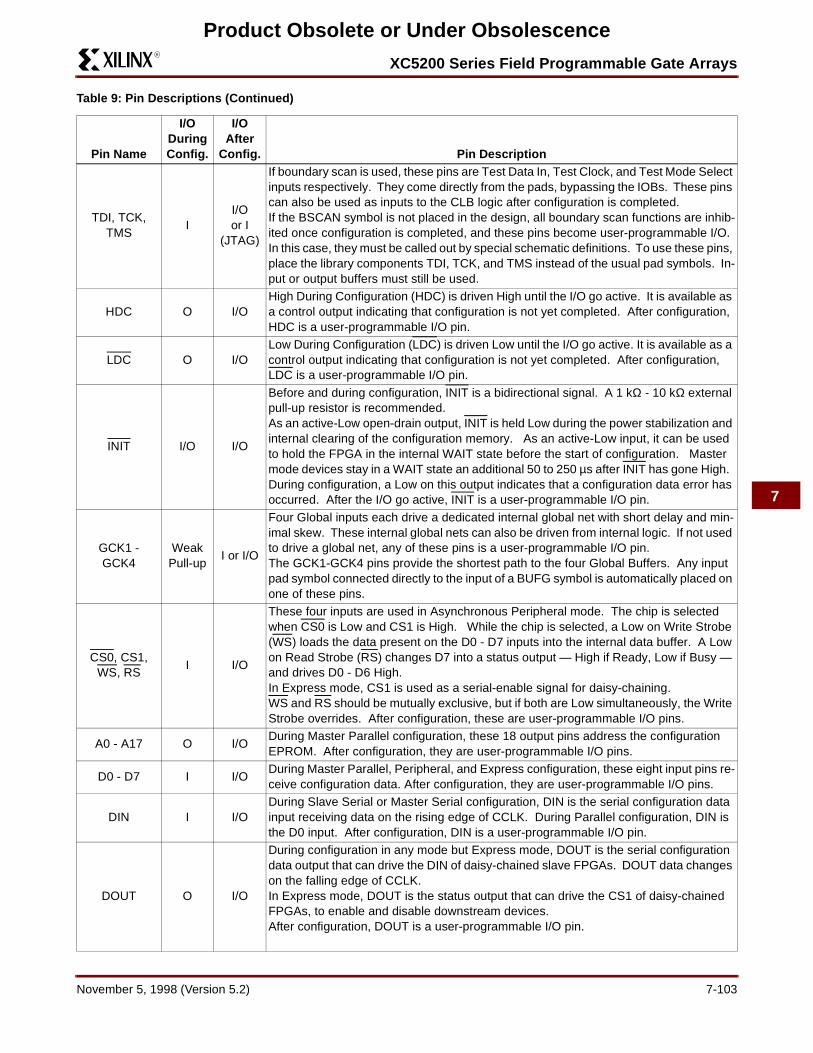
Device pins for XC5200-Series devices are described inTable 9. Pin functions during configuration for each of theseven configuration modes are summarized in “Pin Func-
TDI
TMS
TCK
TDO1
TDO2
TDO
DRCK
IDLE
SEL1
SEL2
RESET
UPDATE
SHIFT
BSCAN
To UserLogic
IBUF
Optional
FromUser Logic
To UserLogic
X9000
Figure 20: Boundary Scan Schematic Example
GND
Ground andVcc Ring forI/O Drivers
Vcc
GND
Vcc
LogicPower Grid
X5422
Figure 21: XC5200-Series Power Distribution
November 5, 1998 (Version 5.2) 7-101

R
XC5200 Series Field Programmable Gate Arrays
Product Obsolete or Under Obsolescence
tions During Configuration” on page 124, in the “Configura-tion Timing” section.
Table 9: Pin Descriptions
Pin Name
I/O During Config.
I/O After
Config. Pin DescriptionPermanently Dedicated Pins
VCC I IFive or more (depending on package) connections to the nominal +5 V supply voltage. All must be connected, and each must be decoupled with a 0.01 - 0.1 µF capacitor to Ground.
GND I IFour or more (depending on package type) connections to Ground. All must be con-nected.
CCLK I or O I
During configuration, Configuration Clock (CCLK) is an output in Master modes or Asyn-chronous Peripheral mode, but is an input in Slave mode, Synchronous Peripheral mode, and Express mode. After configuration, CCLK has a weak pull-up resistor and can be selected as the Readback Clock. There is no CCLK High time restriction on XC5200-Series devices, except during Readback. See “Violating the Maximum High and Low Time Specification for the Readback Clock” on page 113 for an explanation of this exception.
DONE I/O O
DONE is a bidirectional signal with an optional internal pull-up resistor. As an output, it indicates the completion of the configuration process. As an input, a Low level on DONE can be configured to delay the global logic initialization and the enabling of out-puts.The exact timing, the clock source for the Low-to-High transition, and the optional pull-up resistor are selected as options in the program that creates the configuration bit-stream. The resistor is included by default.
PROGRAM I I
PROGRAM is an active Low input that forces the FPGA to clear its configuration mem-ory. It is used to initiate a configuration cycle. When PROGRAM goes High, the FPGA executes a complete clear cycle, before it goes into a WAIT state and releases INIT. The PROGRAM pin has an optional weak pull-up after configuration.
User I/O Pins That Can Have Special Functions
RDY/BUSY O I/O
During Peripheral mode configuration, this pin indicates when it is appropriate to write another byte of data into the FPGA. The same status is also available on D7 in Asyn-chronous Peripheral mode, if a read operation is performed when the device is selected. After configuration, RDY/BUSY is a user-programmable I/O pin. RDY/BUSY is pulled High with a high-impedance pull-up prior to INIT going High.
RCLK O I/O
During Master Parallel configuration, each change on the A0-A17 outputs is preceded by a rising edge on RCLK, a redundant output signal. RCLK is useful for clocked PROMs. It is rarely used during configuration. After configuration, RCLK is a user-pro-grammable I/O pin.
M0, M1, M2 I I/O
As Mode inputs, these pins are sampled before the start of configuration to determine the configuration mode to be used. After configuration, M0, M1, and M2 become us-er-programmable I/O. During configuration, these pins have weak pull-up resistors. For the most popular con-figuration mode, Slave Serial, the mode pins can thus be left unconnected. A pull-down resistor value of 3.3 kΩ is recommended for other modes.
TDO O O
If boundary scan is used, this pin is the Test Data Output. If boundary scan is not used, this pin is a 3-state output, after configuration is completed. This pin can be user output only when called out by special schematic definitions. To use this pin, place the library component TDO instead of the usual pad symbol. An out-put buffer must still be used.
7-102 November 5, 1998 (Version 5.2)
R
XC5200 Series Field Programmable Gate Arrays
7
Product Obsolete or Under Obsolescence
TDI, TCK, TMS
II/Oor I
(JTAG)
If boundary scan is used, these pins are Test Data In, Test Clock, and Test Mode Select inputs respectively. They come directly from the pads, bypassing the IOBs. These pins can also be used as inputs to the CLB logic after configuration is completed. If the BSCAN symbol is not placed in the design, all boundary scan functions are inhib-ited once configuration is completed, and these pins become user-programmable I/O. In this case, they must be called out by special schematic definitions. To use these pins, place the library components TDI, TCK, and TMS instead of the usual pad symbols. In-put or output buffers must still be used.
HDC O I/OHigh During Configuration (HDC) is driven High until the I/O go active. It is available as a control output indicating that configuration is not yet completed. After configuration, HDC is a user-programmable I/O pin.
LDC O I/OLow During Configuration (LDC) is driven Low until the I/O go active. It is available as a control output indicating that configuration is not yet completed. After configuration, LDC is a user-programmable I/O pin.
INIT I/O I/O
Before and during configuration, INIT is a bidirectional signal. A 1 kΩ - 10 kΩ external pull-up resistor is recommended. As an active-Low open-drain output, INIT is held Low during the power stabilization and internal clearing of the configuration memory. As an active-Low input, it can be used to hold the FPGA in the internal WAIT state before the start of configuration. Master mode devices stay in a WAIT state an additional 50 to 250 µs after INIT has gone High. During configuration, a Low on this output indicates that a configuration data error has occurred. After the I/O go active, INIT is a user-programmable I/O pin.
GCK1 - GCK4
Weak Pull-up
I or I/O
Four Global inputs each drive a dedicated internal global net with short delay and min-imal skew. These internal global nets can also be driven from internal logic. If not used to drive a global net, any of these pins is a user-programmable I/O pin. The GCK1-GCK4 pins provide the shortest path to the four Global Buffers. Any input pad symbol connected directly to the input of a BUFG symbol is automatically placed on one of these pins.
CS0, CS1, WS, RS
I I/O
These four inputs are used in Asynchronous Peripheral mode. The chip is selected when CS0 is Low and CS1 is High. While the chip is selected, a Low on Write Strobe (WS) loads the data present on the D0 - D7 inputs into the internal data buffer. A Low on Read Strobe (RS) changes D7 into a status output — High if Ready, Low if Busy — and drives D0 - D6 High. In Express mode, CS1 is used as a serial-enable signal for daisy-chaining.WS and RS should be mutually exclusive, but if both are Low simultaneously, the Write Strobe overrides. After configuration, these are user-programmable I/O pins.
A0 - A17 O I/ODuring Master Parallel configuration, these 18 output pins address the configuration EPROM. After configuration, they are user-programmable I/O pins.
D0 - D7 I I/ODuring Master Parallel, Peripheral, and Express configuration, these eight input pins re-ceive configuration data. After configuration, they are user-programmable I/O pins.
DIN I I/ODuring Slave Serial or Master Serial configuration, DIN is the serial configuration data input receiving data on the rising edge of CCLK. During Parallel configuration, DIN is the D0 input. After configuration, DIN is a user-programmable I/O pin.
DOUT O I/O
During configuration in any mode but Express mode, DOUT is the serial configuration data output that can drive the DIN of daisy-chained slave FPGAs. DOUT data changes on the falling edge of CCLK. In Express mode, DOUT is the status output that can drive the CS1 of daisy-chained FPGAs, to enable and disable downstream devices. After configuration, DOUT is a user-programmable I/O pin.
Table 9: Pin Descriptions (Continued)
Pin Name
I/O During Config.
I/O After
Config. Pin Description
November 5, 1998 (Version 5.2) 7-103

R
XC5200 Series Field Programmable Gate Arrays
Product Obsolete or Under Obsolescence
Configuration Configuration is the process of loading design-specific pro-gramming data into one or more FPGAs to define the func-tional operation of the internal blocks and theirinterconnections. This is somewhat like loading the com-mand registers of a programmable peripheral chip.XC5200-Series devices use several hundred bits of config-uration data per CLB and its associated interconnects.Each configuration bit defines the state of a static memorycell that controls either a function look-up table bit, a multi-plexer input, or an interconnect pass transistor. The devel-opment system translates the design into a netlist file. Itautomatically partitions, places and routes the logic andgenerates the configuration data in PROM format.
Special Purpose Pins Three configuration mode pins (M2, M1, M0) are sampledprior to configuration to determine the configuration mode.After configuration, these pins can be used as auxiliary I/Oconnections. The development system does not use theseresources unless they are explicitly specified in the designentry. This is done by placing a special pad symbol calledMD2, MD1, or MD0 instead of the input or output pad sym-bol.
In XC5200-Series devices, the mode pins have weakpull-up resistors during configuration. With all three modepins High, Slave Serial mode is selected, which is the mostpopular configuration mode. Therefore, for the most com-mon configuration mode, the mode pins can be left uncon-nected. (Note, however, that the internal pull-up resistorvalue can be as high as 100 kΩ.) After configuration, thesepins can individually have weak pull-up or pull-down resis-tors, as specified in the design. A pull-down resistor valueof 3.3kΩ is recommended.
These pins are located in the lower left chip corner and arenear the readback nets. This location allows convenientrouting if compatibility with the XC2000 and XC3000 familyconventions of M0/RT, M1/RD is desired.
Configuration Modes XC5200 devices have seven configuration modes. Thesemodes are selected by a 3-bit input code applied to the M2,
M1, and M0 inputs. There are three self-loading Mastermodes, two Peripheral modes, and a Serial Slave mode,
Note :*Peripheral Synchronous can be considered byte-wideSlave Parallel
which is used primarily for daisy-chained devices. The sev-enth mode, called Express mode, is an additional slavemode that allows high-speed parallel configuration. Thecoding for mode selection is shown in Table 10.
Note that the smallest package, VQ64, only supports theMaster Serial, Slave Serial, and Express modes.A detaileddescription of each configuration mode, with timing infor-mation, is included later in this data sheet. During configu-ration, some of the I/O pins are used temporarily for theconfiguration process. All pins used during configurationare shown in Table 13 on page 124.
Master Modes
The three Master modes use an internal oscillator to gener-ate a Configuration Clock (CCLK) for driving potential slavedevices. They also generate address and timing for exter-nal PROM(s) containing the configuration data.
Master Parallel (Up or Down) modes generate the CCLKsignal and PROM addresses and receive byte paralleldata. The data is internally serialized into the FPGAdata-frame format. The up and down selection generatesstarting addresses at either zero or 3FFFF, for compatibilitywith different microprocessor addressing conventions. The
Unrestricted User-Programmable I/O Pins
I/OWeak Pull-up
I/OThese pins can be configured to be input and/or output after configuration is completed. Before configuration is completed, these pins have an internal high-value pull-up resis-tor (20 kΩ - 100 kΩ) that defines the logic level as High.
Table 9: Pin Descriptions (Continued)
Pin Name
I/O During Config.
I/O After
Config. Pin Description
Table 10: Configuration Modes
Mode M2 M1 M0 CCLK DataMaster Serial 0 0 0 output Bit-Serial
Slave Serial 1 1 1 input Bit-Serial
Master Parallel Up
1 0 0 output Byte-Wide, increment
from 00000
Master Parallel Down
1 1 0 output Byte-Wide, decrement from 3FFFF
Peripheral Synchronous*
0 1 1 input Byte-Wide
Peripheral Asynchronous
1 0 1 output Byte-Wide
Express 0 1 0 input Byte-Wide
Reserved 0 0 1 — —
7-104 November 5, 1998 (Version 5.2)

R
XC5200 Series Field Programmable Gate Arrays
7
Product Obsolete or Under Obsolescence
Master Serial mode generates CCLK and receives the con-figuration data in serial form from a Xilinx serial-configura-tion PROM.
CCLK speed is selectable as 1 MHz (default), 6 MHz, or 12MHz. Configuration always starts at the default slow fre-quency, then can switch to the higher frequency during thefirst frame. Frequency tolerance is -50% to +50%.
Peripheral Modes
The two Peripheral modes accept byte-wide data from abus. A RDY/BUSY status is available as a handshake sig-nal. In Asynchronous Peripheral mode, the internal oscilla-tor generates a CCLK burst signal that serializes thebyte-wide data. CCLK can also drive slave devices. In thesynchronous mode, an externally supplied clock input toCCLK serializes the data.
Slave Serial Mode
In Slave Serial mode, the FPGA receives serial configura-tion data on the rising edge of CCLK and, after loading itsconfiguration, passes additional data out, resynchronizedon the next falling edge of CCLK.
Multiple slave devices with identical configurations can bewired with parallel DIN inputs. In this way, multiple devicescan be configured simultaneously.
Serial Daisy Chain
Multiple devices with different configurations can be con-nected together in a “daisy chain,” and a single combinedbitstream used to configure the chain of slave devices.
To configure a daisy chain of devices, wire the CCLK pinsof all devices in parallel, as shown in Figure 28 on page114. Connect the DOUT of each device to the DIN of thenext. The lead or master FPGA and following slaves eachpasses resynchronized configuration data coming from asingle source. The header data, including the length count,is passed through and is captured by each FPGA when itrecognizes the 0010 preamble. Following the length-countdata, each FPGA outputs a High on DOUT until it hasreceived its required number of data frames.
After an FPGA has received its configuration data, itpasses on any additional frame start bits and configurationdata on DOUT. When the total number of configurationclocks applied after memory initialization equals the valueof the 24-bit length count, the FPGAs begin the start-upsequence and become operational together. FPGA I/O arenormally released two CCLK cycles after the last configura-tion bit is received. Figure 25 on page 109 shows thestart-up timing for an XC5200-Series device.
The daisy-chained bitstream is not simply a concatenationof the individual bitstreams. The PROM file formatter mustbe used to combine the bitstreams for a daisy-chained con-figuration.
Multi-Family Daisy Chain
All Xilinx FPGAs of the XC2000, XC3000, XC4000, andXC5200 Series use a compatible bitstream format and can,therefore, be connected in a daisy chain in an arbitrarysequence. There is, however, one limitation. If the chaincontains XC5200-Series devices, the master normally can-not be an XC2000 or XC3000 device.
The reason for this rule is shown in Figure 25 on page 109.Since all devices in the chain store the same length countvalue and generate or receive one common sequence ofCCLK pulses, they all recognize length-count match on thesame CCLK edge, as indicated on the left edge ofFigure 25. The master device then generates additionalCCLK pulses until it reaches its finish point F. The differentfamilies generate or require different numbers of additionalCCLK pulses until they reach F. Not reaching F means thatthe device does not really finish its configuration, althoughDONE may have gone High, the outputs became active,and the internal reset was released. For theXC5200-Series device, not reaching F means that read-back cannot be initiated and most boundary scan instruc-tions cannot be used.
The user has some control over the relative timing of theseevents and can, therefore, make sure that they occur at theproper time and the finish point F is reached. Timing is con-trolled using options in the bitstream generation software.
XC5200 devices always have the same number of CCLKsin the power up delay, independent of the configurationmode, unlike the XC3000/XC4000 Series devices. To guar-antee all devices in a daisy chain have finished thepower-up delay, tie the INIT pins together, as shown inFigure 27.
XC3000 Master with an XC5200-Series Slave
Some designers want to use an XC3000 lead device inperipheral mode and have the I/O pins of theXC5200-Series devices all available for user I/O. Figure 22provides a solution for that case.
This solution requires one CLB, one IOB and pin, and aninternal oscillator with a frequency of up to 5 MHz as aclock source. The XC3000 master device must be config-ured with late Internal Reset, which is the default option.
One CLB and one IOB in the lead XC3000-family deviceare used to generate the additional CCLK pulse required bythe XC5200-Series devices. When the lead deviceremoves the internal RESET signal, the 2-bit shift registerresponds to its clock input and generates an active Lowoutput signal for the duration of the subsequent clockperiod. An external connection between this output andCCLK thus creates the extra CCLK pulse.
November 5, 1998 (Version 5.2) 7-105

R
XC5200 Series Field Programmable Gate Arrays
Product Obsolete or Under Obsolescence
Express Mode
Express mode is similar to Slave Serial mode, except thedata is presented in parallel format, and is clocked into thetarget device a byte at a time rather than a bit at a time. Thedata is loaded in parallel into eight different columns: it isnot internally serialized. Eight bits of configuration data areloaded with every CCLK cycle, therefore this configurationmode runs at eight times the data rate of the other sixmodes. In this mode the XC5200 family is capable of sup-porting a CCLK frequency of 10 MHz, which is equivalent toan 80 MHz serial rate, because eight bits of configurationdata are being loaded per CCLK cycle. An XC5210 in theExpress mode, for instance, can be configured in about 2ms. The Express mode does not support CRC error check-ing, but does support constant-field error checking. Alength count is not used in Express mode.
In the Express configuration mode, an external signaldrives the CCLK input(s). The first byte of parallel configu-ration data must be available at the D inputs of the FPGAdevices a short set-up time before the second rising CCLKedge. Subsequent data bytes are clocked in on each con-secutive rising CCLK edge. See Figure 38 on page 123.
Bitstream generation currently generates a bitstream suffi-cient to program in all configuration modes except Express.Extra CCLK cycles are necessary to complete the configu-ration, since in this mode data is read at a rate of eight bitsper CCLK cycle instead of one bit per cycle. Normally theentire start-up sequence requires a number of bits that isequal to the number of CCLK cycles needed. An additionalfive CCLKs (equivalent to 40 extra bits) will guarantee com-pletion of configuration, regardless of the start-up optionschosen.
Multiple slave devices with identical configurations can bewired with parallel D0-D7 inputs. In this way, multipledevices can be configured simultaneously.
Pseudo Daisy Chain
Multiple devices with different configurations can be con-nected together in a pseudo daisy chain, provided that all ofthe devices are in Express mode. A single combined bit-stream is used to configure the chain of Express modedevices, but the input data bus must drive D0-D7 of eachdevice. Tie High the CS1 pin of the first device to be config-ured, or leave it floating in the XC5200 since it has an inter-nal pull-up. Connect the DOUT pin of each FPGA to theCS1 pin of the next device in the chain. The D0-D7 inputsare wired to each device in parallel. The DONE pins arewired together, with one or more internal DONE pull-upsactivated. Alternatively, a 4.7 kΩ external resistor can beused, if desired. (See Figure 37 on page 122.) CCLK pinsare tied together.
The requirement that all DONE pins in a daisy chain bewired together applies only to Express mode, and only if alldevices in the chain are to become active simultaneously.All devices in Express mode are synchronized to the DONEpin. User I/O for each device become active after theDONE pin for that device goes High. (The exact timing isdetermined by options to the bitstream generation soft-ware.) Since the DONE pin is open-drain and does notdrive a High value, tying the DONE pins of all devicestogether prevents all devices in the chain from going Highuntil the last device in the chain has completed its configu-ration cycle.
The status pin DOUT is pulled LOW two internal-oscillatorcycles (nominally 1 MHz) after INIT is recognized as High,and remains Low until the device’s configuration memory isfull. Then DOUT is pulled High to signal the next device inthe chain to accept the configuration data on the D7-D0bus. All devices receive and recognize the six bytes of pre-amble and length count, irrespective of the level on CS1;but subsequent frame data is accepted only when CS1 isHigh and the device’s configuration memory is not alreadyfull.
Setting CCLK FrequencyFor Master modes, CCLK can be generated in one of threefrequencies. In the default slow mode, the frequency isnominally 1 MHz. In fast CCLK mode, the frequency isnominally 12 MHz. In medium CCLK mode, the frequencyis nominally 6 MHz. The frequency range is -50% to +50%.The frequency is selected by an option when running thebitstream generation software. If an XC5200-Series Masteris driving an XC3000- or XC2000-family slave, slow CCLKmode must be used. Slow mode is the default.
OutputConnectedto CCLK
OE/T
01100..
00111..
Reset
X5223etc
Active Low OutputActive High Output
Figure 22: CCLK Generation for XC3000 Master Driving an XC5200-Series Slave
Table 11: XC5200 Bitstream Format
Data Type Value Occurrences
Fill Byte 11111111 Once per bit-streamPreamble 11110010
Length Counter COUNT(23:0)Fill Byte 11111111
7-106 November 5, 1998 (Version 5.2)

R
XC5200 Series Field Programmable Gate Arrays
7
Product Obsolete or Under Obsolescence
Data Stream Format The data stream (“bitstream”) format is identical for all con-figuration modes, with the exception of Express mode. InExpress mode, the device becomes active when DONEgoes High, therefore no length count is required. Addition-ally, CRC error checking is not supported in Express mode.
The data stream formats are shown in Table 11. Expressmode data is shown with D0 at the left and D7 at the right.For all other modes, bit-serial data is read from left to right,and byte-parallel data is effectively assembled from thisserial bitstream, with the first bit in each byte assigned toD0.
The configuration data stream begins with a string of eightones, a preamble code, followed by a 24-bit length countand a separator field of ones (or 24 fill bits, in Expressmode). This header is followed by the actual configurationdata in frames. The length and number of frames dependson the device type (see Table 12). Each frame begins witha start field and ends with an error check. In all modesexcept Express mode, a postamble code is required to sig-nal the end of data for a single device. In all cases, addi-tional start-up bytes of data are required to provide fourclocks for the startup sequence at the end of configuration.Long daisy chains require additional startup bytes to shiftthe last data through the chain. All startup bytes aredon’t-cares; these bytes are not included in bitstreams cre-ated by the Xilinx software.
In Express mode, only non-CRC error checking is sup-ported. In all other modes, a selection of CRC or non-CRCerror checking is allowed by the bitstream generation soft-ware. The non-CRC error checking tests for a designatedend-of-frame field for each frame. For CRC error checking,the software calculates a running CRC and inserts a uniquefour-bit partial check at the end of each frame. The 11-bitCRC check of the last frame of an FPGA includes the lastseven data bits.
Detection of an error results in the suspension of data load-ing and the pulling down of the INIT pin. In Master modes,
CCLK and address signals continue to operate externally.The user must detect INIT and initialize a new configurationby pulsing the PROGRAM pin Low or cycling Vcc.
Cyclic Redundancy Check (CRC) for Configuration and ReadbackThe Cyclic Redundancy Check is a method of error detec-tion in data transmission applications. Generally, the trans-mitting system performs a calculation on the serialbitstream. The result of this calculation is tagged onto thedata stream as additional check bits. The receiving systemperforms an identical calculation on the bitstream and com-pares the result with the received checksum.
Each data frame of the configuration bitstream has fourerror bits at the end, as shown in Table 11. If a frame dataerror is detected during the loading of the FPGA, the con-figuration process with a potentially corrupted bitstream isterminated. The FPGA pulls the INIT pin Low and goes intoa Wait state.
During Readback, 11 bits of the 16-bit checksum are addedto the end of the Readback data stream. The checksum iscomputed using the CRC-16 CCITT polynomial, as shownin Figure 23. The checksum consists of the 11 most signifi-cant bits of the 16-bit code. A change in the checksum indi-cates a change in the Readback bitstream. A comparisonto a previous checksum is meaningful only if the readbackdata is independent of the current device state. CLB out-puts should not be included (Read Capture option notused). Statistically, one error out of 2048 might go undetec-ted.
Start Byte 11111110 Once per data frameData Frame * DATA(N-1:0)
Cyclic Redundancy Check orConstant Field Check
CRC(3:0) or0110
Fill Nibble 1111Extend Write Cycle FFFFFFPostamble 11111110 Once per de-
viceFill Bytes (30) FFFF…FFStart-Up Byte FF Once per bit-
stream*Bits per Frame (N) depends on device size, as described for table 11.
Table 11: XC5200 Bitstream Format
Data Type Value Occurrences
Table 12: Internal Configuration Data Structure
DeviceVersaBlock
Array
PROMSize(bits)
XilinxSerial PROM
Needed
XC5202 8 x 8 42,416 XC1765EXC5204 10 x 12 70,704 XC17128EXC5206 14 x 14 106,288 XC17128EXC5210 18 x 18 165,488 XC17256EXC5215 22 x 22 237,744 XC17256EBits per Frame = (34 x number of Rows) + 28 for the top + 28 for the bottom + 4 splitter bits + 8 start bits + 4 error check bits + 4 fill bits * + 24 extended write bits= (34 x number of Rows) + 100* In the XC5202 (8 x 8), there are 8 fill bits per frame, not 4Number of Frames = (12 x number of Columns) + 7 for the left edge + 8 for the right edge + 1 splitter bit= (12 x number of Columns) + 16Program Data = (Bits per Frame x Number of Frames) + 48 header bits + 8 postamble bits + 240 fill bits + 8 start-up bits= (Bits per Frame x Number of Frames) + 304PROM Size = Program Data
November 5, 1998 (Version 5.2) 7-107

R
XC5200 Series Field Programmable Gate Arrays
Product Obsolete or Under Obsolescence
Configuration Sequence There are four major steps in the XC5200-Series power-upconfiguration sequence.
• Power-On Time-Out• Initialization• Configuration• Start-Up
The full process is illustrated in Figure 24.
Power-On Time-Out
An internal power-on reset circuit is triggered when poweris applied. When VCC reaches the voltage at which portionsof the FPGA begin to operate (i.e., performs awrite-and-read test of a sample pair of configuration mem-ory bits), the programmable I/O buffers are 3-stated withactive high-impedance pull-up resistors. A time-out delay— nominally 4 ms — is initiated to allow the power-supplyvoltage to stabilize. For correct operation the power supplymust reach VCC(min) by the end of the time-out, and mustnot dip below it thereafter.
There is no distinction between master and slave modeswith regard to the time-out delay. Instead, the INIT line isused to ensure that all daisy-chained devices have com-pleted initialization. Since XC2000 devices do not have thissignal, extra care must be taken to guarantee proper oper-ation when daisy-chaining them with XC5200 devices. Forproper operation with XC3000 devices, the RESET signal,which is used in XC3000 to delay configuration, should beconnected to INIT.
If the time-out delay is insufficient, configuration should bedelayed by holding the INIT pin Low until the power supplyhas reached operating levels.
This delay is applied only on power-up. It is not appliedwhen reconfiguring an FPGA by pulsing the PROGRAMpin Low. During all three phases — Power-on, Initialization,and Configuration — DONE is held Low; HDC, LDC, andINIT are active; DOUT is driven; and all I/O buffers are dis-abled.
Initialization
This phase clears the configuration memory and estab-lishes the configuration mode.
The configuration memory is cleared at the rate of oneframe per internal clock cycle (nominally 1 MHz). Anopen-drain bidirectional signal, INIT, is released when theconfiguration memory is completely cleared. The devicethen tests for the absence of an external active-low level onINIT. The mode lines are sampled two internal clock cycleslater (nominally 2 µs).
The master device waits an additional 32 µs to 256 µs(nominally 64-128 µs) to provide adequate time for all of theslave devices to recognize the release of INIT as well. Thenthe master device enters the Configuration phase.
0
X2
2 3 4 5 6 7 8 9 10 11 12 13 141
X15X16
15
SERIAL DATA IN
1 0 15 14 13 12 11 10 9 8 7 6 51111
CRC – CHECKSUMLAST DATA FRAME
ST
AR
T B
IT
X1789
Polynomial: X16 + X15 + X2 + 1
Readback Data Stream
Figure 23: Circuit for Generating CRC-16
Figure 24: Configuration Sequence
INITHigh? ifMaster
SampleMode Lines
Load OneConfigurationData Frame
FrameError
PassConfigurationData to DOUT
VCC3V
No
Yes
Yes
No
No
Yes
Operational
Start-UpSequence
No
Yes
~1.3 µs per Frame
Master CCLKGoes Active after
50 to 250 µs
F
Pull INIT Lowand Stop
X9017
EXTEST*SAMPLE/PRELOAD*
BYPASSCONFIGURE*
(*only when PROGRAM = High)
SAMPLE/PRELOADBYPASS
EXTESTSAMPLE PRELOAD
BYPASSUSER 1USER 2
CONFIGUREREADBACK
If Boundary Scanis Selected
Config-urationmemory
Full
CCLKCount Equals
LengthCount
Completely ClearConfiguration
Memory
LD
C O
utp
ut
= L
, HD
C O
utp
ut
= H
Boundary ScanInstructionsAvailable:
I/O A
ctiv
e
GenerateOne Time-Out Pulse
of 4 msPROGRAM
= Low
No
Yes
Yes
7-108 November 5, 1998 (Version 5.2)

R
XC5200 Series Field Programmable Gate Arrays
7
Product Obsolete or Under Obsolescence
XC4000E/EXXC5200/
UCLK_SYNC
XC4000E/EXXC5200/
UCLK_NOSYNC
XC4000E/EXXC5200/
CCLK_SYNC
XC4000E/EXXC5200/
CCLK_NOSYNC
XC3000
XC2000
CCLK
GSR Active
UCLK Period
DONE IN
DONE IN
Di Di+1 Di+2
Di Di+1 Di+2
U2 U3 U4
U2 U3 U4
U2 U3 U4C1
SynchronizationUncertainty
Di Di+1
Di Di+1
DONE
I/O
GSR Active
DONE
I/O
GSR Active
DONE
C1 C2
C1 U2
C3 C4
C2 C3 C4
C2 C3 C4
I/O
GSR Active
DONE
I/O
DONE
Global Reset
I/O
DONE
Global Reset
I/O
F = Finished, no moreconfiguration clocks neededDaisy-chain lead devicemust have latest F
Heavy lines describedefault timing
CCLK PeriodLength Count Match
F
F
F
F
F
F
X6700
C1, C2 or C3
Figure 25: Start-up Timing
November 5, 1998 (Version 5.2) 7-109
R
XC5200 Series Field Programmable Gate Arrays
Product Obsolete or Under Obsolescence
ConfigurationThe length counter begins counting immediately upon entryinto the configuration state. In slave-mode operation it isimportant to wait at least two cycles of the internal 1-MHzclock oscillator after INIT is recognized before togglingCCLK and feeding the serial bitstream. Configuration willnot begin until the internal configuration logic reset isreleased, which happens two cycles after INIT goes High.A master device’s configuration is delayed from 32 to 256µs to ensure proper operation with any slave devices drivenby the master device.
The 0010 preamble code, included for all modes exceptExpress mode, indicates that the following 24 bits repre-sent the length count. The length count is the total numberof configuration clocks needed to load the complete config-uration data. (Four additional configuration clocks arerequired to complete the configuration process, as dis-cussed below.) After the preamble and the length counthave been passed through to all devices in the daisy chain,DOUT is held High to prevent frame start bits from reachingany daisy-chained devices. In Express mode, the lengthcount bits are ignored, and DOUT is held Low, to disablethe next device in the pseudo daisy chain.
A specific configuration bit, early in the first frame of a mas-ter device, controls the configuration-clock rate and canincrease it by a factor of eight. Therefore, if a fast configu-ration clock is selected by the bitstream, the slower clockrate is used until this configuration bit is detected.
Each frame has a start field followed by the frame-configu-ration data bits and a frame error field. If a frame data erroris detected, the FPGA halts loading, and signals the errorby pulling the open-drain INIT pin Low. After all configura-tion frames have been loaded into an FPGA, DOUT againfollows the input data so that the remaining data is passedon to the next device. In Express mode, when the firstdevice is fully programmed, DOUT goes High to enable thenext device in the chain.
Delaying Configuration After Power-Up
To delay master mode configuration after power-up, pullthe bidirectional INIT pin Low, using an open-collector(open-drain) driver. (See Figure 12.)
Using an open-collector or open-drain driver to hold INITLow before the beginning of master mode configurationcauses the FPGA to wait after completing the configurationmemory clear operation. When INIT is no longer held Lowexternally, the device determines its configuration mode bycapturing its mode pins, and is ready to start the configura-tion process. A master device waits up to an additional 250µs to make sure that any slaves in the optional daisy chainhave seen that INIT is High.
Start-Up
Start-up is the transition from the configuration process tothe intended user operation. This transition involves achange from one clock source to another, and a changefrom interfacing parallel or serial configuration data wheremost outputs are 3-stated, to normal operation with I/O pinsactive in the user-system. Start-up must make sure thatthe user-logic ‘wakes up’ gracefully, that the outputsbecome active without causing contention with the configu-ration signals, and that the internal flip-flops are releasedfrom the global Reset at the right time.
Figure 25 describes start-up timing for the three Xilinx fam-ilies in detail. Express mode configuration always useseither CCLK_SYNC or UCLK_SYNC timing, the other con-figuration modes can use any of the four timing sequences.
To access the internal start-up signals, place the STARTUPlibrary symbol.
Start-up Timing
Different FPGA families have different start-up sequences.
The XC2000 family goes through a fixed sequence. DONEgoes High and the internal global Reset is de-activated oneCCLK period after the I/O become active.
The XC3000A family offers some flexibility. DONE can beprogrammed to go High one CCLK period before or afterthe I/O become active. Independent of DONE, the internalglobal Reset is de-activated one CCLK period before orafter the I/O become active.
The XC4000/XC5200 Series offers additional flexibility.The three events — DONE going High, the internal Resetbeing de-activated, and the user I/O going active — can alloccur in any arbitrary sequence. Each of them can occurone CCLK period before or after, or simultaneous with, anyof the others. This relative timing is selected by means ofsoftware options in the bitstream generation software.
The default option, and the most practical one, is for DONEto go High first, disconnecting the configuration data sourceand avoiding any contention when the I/Os become activeone clock later. Reset is then released another clock periodlater to make sure that user-operation starts from stableinternal conditions. This is the most common sequence,shown with heavy lines in Figure 25, but the designer canmodify it to meet particular requirements.
Normally, the start-up sequence is controlled by the internaldevice oscillator output (CCLK), which is asynchronous tothe system clock.
XC4000/XC5200 Series offers another start-up clockingoption, UCLK_NOSYNC. The three events describedabove need not be triggered by CCLK. They can, as a con-figuration option, be triggered by a user clock. This meansthat the device can wake up in synchronism with the usersystem.
7-110 November 5, 1998 (Version 5.2)

R
XC5200 Series Field Programmable Gate Arrays
7
Product Obsolete or Under Obsolescence
When the UCLK_SYNC option is enabled, the user canexternally hold the open-drain DONE output Low, and thusstall all further progress in the start-up sequence untilDONE is released and has gone High. This option can beused to force synchronization of several FPGAs to a com-mon user clock, or to guarantee that all devices are suc-cessfully configured before any I/Os go active.
If either of these two options is selected, and no user clockis specified in the design or attached to the device, the chipcould reach a point where the configuration of the device iscomplete and the Done pin is asserted, but the outputs donot become active. The solution is either to recreate thebitstream specifying the start-up clock as CCLK, or to sup-ply the appropriate user clock.
Start-up Sequence
The Start-up sequence begins when the configurationmemory is full, and the total number of configuration clocksreceived since INIT went High equals the loaded value ofthe length count.
The next rising clock edge sets a flip-flop Q0, shown inFigure 26. Q0 is the leading bit of a 5-bit shift register. Theoutputs of this register can be programmed to control threeevents.
• The release of the open-drain DONE output• The change of configuration-related pins to the user
function, activating all IOBs. • The termination of the global Set/Reset initialization of
all CLB and IOB storage elements.
The DONE pin can also be wire-ANDed with DONE pins ofother FPGAs or with other external signals, and can thenbe used as input to bit Q3 of the start-up register. This iscalled “Start-up Timing Synchronous to Done In” and isselected by either CCLK_SYNC or UCLK_SYNC.
When DONE is not used as an input, the operation is called“Start-up Timing Not Synchronous to DONE In,” and isselected by either CCLK_NOSYNC or UCLK_NOSYNC.
As a configuration option, the start-up control registerbeyond Q0 can be clocked either by subsequent CCLKpulses or from an on-chip user net called STARTUP.CLK.These signals can be accessed by placing the STARTUPlibrary symbol.
Start-up from CCLK
If CCLK is used to drive the start-up, Q0 through Q3 pro-vide the timing. Heavy lines in Figure 25 show the defaulttiming, which is compatible with XC2000 and XC3000devices using early DONE and late Reset. The thin linesindicate all other possible timing options.
Start-up from a User Clock (STARTUP.CLK)
When, instead of CCLK, a user-supplied start-up clock isselected, Q1 is used to bridge the unknown phase relation-
ship between CCLK and the user clock. This arbitrationcauses an unavoidable one-cycle uncertainty in the timingof the rest of the start-up sequence.
DONE Goes High to Signal End of Configuration
In all configuration modes except Express mode,XC5200-Series devices read the expected length countfrom the bitstream and store it in an internal register. Thelength count varies according to the number of devices andthe composition of the daisy chain. Each device alsocounts the number of CCLKs during configuration.
Two conditions have to be met in order for the DONE pin togo high:
• the chip's internal memory must be full, and• the configuration length count must be met, exactly.
This is important because the counter that determineswhen the length count is met begins with the very firstCCLK, not the first one after the preamble.
Therefore, if a stray bit is inserted before the preamble, orthe data source is not ready at the time of the first CCLK,the internal counter that holds the number of CCLKs will beone ahead of the actual number of data bits read. At theend of configuration, the configuration memory will be full,but the number of bits in the internal counter will not matchthe expected length count.
As a consequence, a Master mode device will continue tosend out CCLKs until the internal counter turns over tozero, and then reaches the correct length count a secondtime. This will take several seconds [224 ∗ CCLK period]— which is sometimes interpreted as the device not config-uring at all.
If it is not possible to have the data ready at the time of thefirst CCLK, the problem can be avoided by increasing thenumber in the length count by the appropriate value.
In Express mode, there is no length count. The DONE pinfor each device goes High when the device has received itsquota of configuration data. Wiring the DONE pins of sev-eral devices together delays start-up of all devices until allare fully configured.
Note that DONE is an open-drain output and does not goHigh unless an internal pull-up is activated or an externalpull-up is attached. The internal pull-up is activated as thedefault by the bitstream generation software.
Release of User I/O After DONE Goes High
By default, the user I/O are released one CCLK cycle afterthe DONE pin goes High. If CCLK is not clocked afterDONE goes High, the outputs remain in their initial state —3-stated, with a 20 kΩ - 100 kΩ pull-up. The delay from
November 5, 1998 (Version 5.2) 7-111

R
XC5200 Series Field Programmable Gate Arrays
Product Obsolete or Under Obsolescence
DONE High to active user I/O is controlled by an option tothe bitstream generation software.
Release of Global Reset After DONE Goes High
By default, Global Reset (GR) is released two CCLK cyclesafter the DONE pin goes High. If CCLK is not clocked twiceafter DONE goes High, all flip-flops are held in their initialreset state. The delay from DONE High to GR inactive iscontrolled by an option to the bitstream generation soft-ware.
Configuration Complete After DONE Goes High
Three full CCLK cycles are required after the DONE pingoes High, as shown in Figure 25 on page 109. If CCLK isnot clocked three times after DONE goes High, readbackcannot be initiated and most boundary scan instructionscannot be used.
Configuration Through the Boundary Scan PinsXC5200-Series devices can be configured through theboundary scan pins.
For detailed information, refer to the Xilinx application noteXAPP017, “Boundary Scan in XC4000 and XC5200Devices.”
ReadbackThe user can read back the content of configuration mem-ory and the level of certain internal nodes without interfer-ing with the normal operation of the device.
Readback not only reports the downloaded configurationbits, but can also include the present state of the device,represented by the content of all flip-flops and latches inCLBs.
DONE
*
*
*
*
* *
Q S
R
1
0
0
1
1
0
1
0
1
0
0
1
GR ENABLEGR INVERTSTARTUP.GR
STARTUP.GTSGTS INVERTGTS ENABLE
CONTROLLED BY STARTUP SYMBOLIN THE USER SCHEMATIC (SEELIBRARIES GUIDE)
GLOBAL RESET OFALL CLB FLIP-FLOPS/LATCHES
IOBs OPERATIONAL PER CONFIGURATION
GLOBAL 3-STATE OF ALL IOBs
Q2
Q3 Q1/Q4DONEIN
STARTUP
Q0 Q1 Q2 Q3 Q4
M
M
" FINISHED "ENABLES BOUNDARYSCAN, READBACK ANDCONTROLS THE OSCILLATOR
K
S Q
K
D Q
K
D Q
K
D Q
K
D QFULL
LENGTH COUNT
CLEAR MEMORY
CCLK
STARTUP.CLKUSER NET
CONFIGURATION BIT OPTIONS SELECTED BY USERX9002
Figure 26: Start-up Logic
7-112 November 5, 1998 (Version 5.2)

R
XC5200 Series Field Programmable Gate Arrays
7
Product Obsolete or Under Obsolescence
Note that in XC5200-Series devices, configuration data isnot inverted with respect to configuration as it is in XC2000and XC3000 families.
Readback of Express mode bitstreams results in data thatdoes not resemble the original bitstream, because the bit-stream format differs from other modes.
XC5200-Series Readback does not use any dedicatedpins, but uses four internal nets (RDBK.TRIG,RDBK.DATA, RDBK.RIP and RDBK.CLK) that can berouted to any IOB. To access the internal Readback sig-nals, place the READBACK library symbol and attach theappropriate pad symbols, as shown in Figure 27.
After Readback has been initiated by a Low-to-High transi-tion on RDBK.TRIG, the RDBK.RIP (Read In Progress)output goes High on the next rising edge of RDBK.CLK.Subsequent rising edges of this clock shift out Readbackdata on the RDBK.DATA net.
Readback data does not include the preamble, but startswith five dummy bits (all High) followed by the Start bit(Low) of the first frame. The first two data bits of the firstframe are always High.
Each frame ends with four error check bits. They are readback as High. The last seven bits of the last frame are alsoread back as High. An additional Start bit (Low) and an11-bit Cyclic Redundancy Check (CRC) signature follow,before RDBK.RIP returns Low.
Readback OptionsReadback options are: Read Capture, Read Abort, andClock Select. They are set with the bitstream generationsoftware.
Read Capture
When the Read Capture option is selected, the readbackdata stream includes sampled values of CLB and IOB sig-nals. The rising edge of RDBK.TRIG latches the invertedvalues of the CLB outputs and the IOB output and input sig-nals. Note that while the bits describing configuration(interconnect and function generators) are not inverted, theCLB and IOB output signals are inverted.
When the Read Capture option is not selected, the valuesof the capture bits reflect the configuration data originallywritten to those memory locations.
The readback signals are located in the lower-left corner ofthe device.
Read Abort
When the Read Abort option is selected, a High-to-Lowtransition on RDBK.TRIG terminates the readback opera-tion and prepares the logic to accept another trigger.
After an aborted readback, additional clocks (up to onereadback clock per configuration frame) may be required tore-initialize the control logic. The status of readback is indi-cated by the output control net RDBK.RIP. RDBK.RIP isHigh whenever a readback is in progress.
Clock Select
CCLK is the default clock. However, the user can insertanother clock on RDBK.CLK. Readback control and dataare clocked on rising edges of RDBK.CLK. If readbackmust be inhibited for security reasons, the readback controlnets are simply not connected.
Violating the Maximum High and Low Time Specification for the Readback ClockThe readback clock has a maximum High and Low timespecification. In some cases, this specification cannot bemet. For example, if a processor is controlling readback,an interrupt may force it to stop in the middle of a readback.This necessitates stopping the clock, and thus violating thespecification.
The specification is mandatory only on clocking data at theend of a frame prior to the next start bit. The transfer mech-anism will load the data to a shift register during the last sixclock cycles of the frame, prior to the start bit of the follow-ing frame. This loading process is dynamic, and is thesource of the maximum High and Low time requirements.
Therefore, the specification only applies to the six clockcycles prior to and including any start bit, including theclocks before the first start bit in the readback data stream.At other times, the frame data is already in the register andthe register is not dynamic. Thus, it can be shifted out justlike a regular shift register.
The user must precisely calculate the location of the read-back data relative to the frame. The system must keeptrack of the position within a data frame, and disable inter-rupts before frame boundaries. Frame lengths and data for-mats are listed in Table 11 and Table 12.
Readback with the XChecker CableThe XChecker Universal Download/Readback Cable andLogic Probe uses the readback feature for bitstream verifi-cation. It can also display selected internal signals on thePC or workstation screen, functioning as a low-cost in-cir-cuit emulator.
READBACK
DATA
RIPTRIG
CLK READ_DATA
OBUF
MD1
MD0READ_TRIGGER
IBUF X1786
IF UNCONNECTED,DEFAULT IS CCLK
Figure 27: Readback Schematic Example
November 5, 1998 (Version 5.2) 7-113

R
XC5200 Series Field Programmable Gate Arrays
Product Obsolete or Under Obsolescence
Configuration TimingThe seven configuration modes are discussed in detail inthis section. Timing specifications are included.
Slave Serial ModeIn Slave Serial mode, an external signal drives the CCLKinput of the FPGA. The serial configuration bitstream mustbe available at the DIN input of the lead FPGA a shortsetup time before each rising CCLK edge.
The lead FPGA then presents the preamble data—and alldata that overflows the lead device—on its DOUT pin.
There is an internal delay of 0.5 CCLK periods, whichmeans that DOUT changes on the falling CCLK edge, andthe next FPGA in the daisy chain accepts data on the sub-sequent rising CCLK edge.
Figure 28 shows a full master/slave system. AnXC5200-Series device in Slave Serial mode should be con-nected as shown in the third device from the left.
Slave Serial mode is selected by a <111> on the mode pins(M2, M1, M0). Slave Serial is the default mode if the modepins are left unconnected, as they have weak pull-up resis-tors during configuration.
Note: Configuration must be delayed until the INIT pins of all daisy-chained FPGAs are High.Figure 29: Slave Serial Mode Programming Switching Characteristics
XC5200MASTERSERIAL
Spartan,XC4000E/EX,
XC5200SLAVE
XC3100ASLAVE
XC1700E
PROGRAM
NOTE:M2, M1, M0 can be shortedto Ground if not used as I/O
NOTE:M2, M1, M0 can be shortedto VCC if not used as I/O
M2M0 M1
DOUT
CCLK CLK
VCC
+5 V
DATA
CE CEO
VPP
RESET/OE DONE
DIN
LDCINIT INITDONE
PROGRAM PROGRAMD/P INITRESET
CCLK
DIN
CCLK
DINDOUT DOUT
M2M0 M1 M1 PWRDNM0
M2
(Low Reset Option Used)
4.7 KΩ
3.3 KΩ3.3 KΩ3.3 KΩ 3.3 KΩ3.3 KΩ3.3 KΩ
VCC
X9003_01
N/C
N/C
Figure 28: Master/Slave Serial Mode Circuit Diagram
4 TCCH
Bit n Bit n + 1
Bit nBit n - 1
3 TCCO
5 TCCL2 TCCD1 TDCC
DIN
CCLK
DOUT(Output)
X5379
Description Symbol Min Max Units
CCLK
DIN setup 1 TDCC 20 ns
DIN hold 2 TCCD 0 ns
DIN to DOUT 3 TCCO 30 ns
High time 4 TCCH 45 ns
Low time 5 TCCL 45 ns
Frequency FCC 10 MHz
7-114 November 5, 1998 (Version 5.2)

R
XC5200 Series Field Programmable Gate Arrays
7
Product Obsolete or Under Obsolescence
Master Serial ModeIn Master Serial mode, the CCLK output of the lead FPGAdrives a Xilinx Serial PROM that feeds the FPGA DIN input.Each rising edge of the CCLK output increments the SerialPROM internal address counter. The next data bit is put onthe SPROM data output, connected to the FPGA DIN pin.The lead FPGA accepts this data on the subsequent risingCCLK edge.
The lead FPGA then presents the preamble data—and alldata that overflows the lead device—on its DOUT pin.There is an internal pipeline delay of 1.5 CCLK periods,which means that DOUT changes on the falling CCLKedge, and the next FPGA in the daisy chain accepts dataon the subsequent rising CCLK edge.
In the bitstream generation software, the user can specifyFast ConfigRate, which, starting several bits into the firstframe, increases the CCLK frequency by a factor of twelve.
The value increases from a nominal 1 MHz, to a nominal 12MHz. Be sure that the serial PROM and slaves are fastenough to support this data rate. The Medium ConfigRateoption changes the frequency to a nominal 6 MHz.XC2000, XC3000/A, and XC3100A devices do not supportthe Fast or Medium ConfigRate options.
The SPROM CE input can be driven from either LDC orDONE. Using LDC avoids potential contention on the DINpin, if this pin is configured as user-I/O, but LDC is thenrestricted to be a permanently High user output after con-figuration. Using DONE can also avoid contention on DIN,provided the DONE before I/O enable option is invoked.
Figure 28 on page 114 shows a full master/slave system.The leftmost device is in Master Serial mode.
Master Serial mode is selected by a <000> on the modepins (M2, M1, M0).
Notes: 1. At power-up, Vcc must rise from 2.0 V to Vcc min in less than 25 ms, otherwise delay configuration by pulling PROGRAM Low until Vcc is valid.
2. Master Serial mode timing is based on testing in slave mode.
Figure 30: Master Serial Mode Programming Switching Characteristics
In the two Master Parallel modes, the lead FPGA directlyaddresses an industry-standard byte-wide EPROM, andaccepts eight data bits just before incrementing or decre-menting the address outputs.
The eight data bits are serialized in the lead FPGA, whichthen presents the preamble data—and all data that over-flows the lead device—on its DOUT pin. There is an inter-nal delay of 1.5 CCLK periods, after the rising CCLK edgethat accepts a byte of data (and also changes the EPROMaddress) until the falling CCLK edge that makes the LSB(D0) of this byte appear at DOUT. This means that DOUTchanges on the falling CCLK edge, and the next FPGA inthe daisy chain accepts data on the subsequent risingCCLK edge.
The PROM address pins can be incremented or decre-mented, depending on the mode pin settings. This optionallows the FPGA to share the PROM with a wide variety ofmicroprocessors and microcontrollers. Some processorsmust boot from the bottom of memory (all zeros) while oth-ers must boot from the top. The FPGA is flexible and canload its configuration bitstream from either end of the mem-ory.
Master Parallel Up mode is selected by a <100> on themode pins (M2, M1, M0). The EPROM addresses start at00000 and increment.
Master Parallel Down mode is selected by a <110> on themode pins. The EPROM addresses start at 3FFFF anddecrement.
Serial Data In
CCLK(Output)
Serial DOUT(Output)
1 TDSCK
2 TCKDS
n n + 1 n + 2
n – 3 n – 2 n – 1 n
X3223
Description Symbol Min Max Units
CCLKDIN setup 1 TDSCK 20 ns
DIN hold 2 TCKDS 0 ns
November 5, 1998 (Version 5.2) 7-115

R
XC5200 Series Field Programmable Gate Arrays
Product Obsolete or Under Obsolescence
M0 M1
DOUT
VCC
M2
PROGRAM
D7
D6
D5
D4
D3
D2
D1
D0
PROGRAM
CCLK
DIN
M0 M1 M2
DOUT
PROGRAM
EPROM(8K x 8)
(OR LARGER)
A10
A11
A12
A9
A8
A7
A6
A5
A4
A3
A2
A1
A0
D7
DONE
D6
D5
D4
D3
D2
D1
D0
N/C
N/C
CE
OE
XC5200/XC4000E/EX/
SpartanSLAVE
8DATA BUS
CCLK
A15
A14
A13
A12
A11
A10
A9
A8
A7
A6
A5
A4
A3
A2
A1
A0
INIT
INIT
. . .
. . .
. . .USER CONTROL OF HIGHERORDER PROM ADDRESS BITSCAN BE USED TO SELECT BETWEENALTERNATIVE CONFIGURATIONS
DONE
TO DIN OF OPTIONALDAISY-CHAINED FPGAS
A16 . . .
A17 . . .
HIGH or
LOW
X9004_01
TO CCLK OF OPTIONALDAISY-CHAINED FPGAS
3.3 K
4.7K
NOTE:M0 can be shortedto Ground if not usedas I/O.
XC5200MasterParallel
Figure 31: Master Parallel Mode Circuit Diagram
7-116 November 5, 1998 (Version 5.2)

R
XC5200 Series Field Programmable Gate Arrays
7
Product Obsolete or Under Obsolescence
.
Note: 1. At power-up, VCC must rise from 2.0 V to VCC min in less then 25 ms, otherwise delay configuration by pulling PROGRAM Low until VCC is Valid.
2. The first Data byte is loaded and CCLK starts at the end of the first RCLK active cycle (rising edge).
This timing diagram shows that the EPROM requirements are extremely relaxed. EPROM access time can be longer than500 ns. EPROM data output has no hold-time requirements.
Figure 32: Master Parallel Mode Programming Switching Characteristics
Address for Byte n
Byte
2 TDRC
Address for Byte n + 1
D7D6
A0-A17(output)
D0-D7
RCLK(output)
CCLK(output)
DOUT(output)
1 TRAC
7 CCLKs CCLK
3 TRCD
Byte n - 1 X6078
Description Symbol Min Max Units
CCLK
Delay to Address valid 1 TRAC 0 200 ns
Data setup time 2 TDRC 60 ns
Data hold time 3 TRCD 0 ns
November 5, 1998 (Version 5.2) 7-117

R
XC5200 Series Field Programmable Gate Arrays
Product Obsolete or Under Obsolescence
Synchronous Peripheral ModeSynchronous Peripheral mode can also be consideredSlave Parallel mode. An external signal drives the CCLKinput(s) of the FPGA(s). The first byte of parallel configura-tion data must be available at the Data inputs of the leadFPGA a short setup time before the rising CCLK edge.Subsequent data bytes are clocked in on every eighth con-secutive rising CCLK edge.
The same CCLK edge that accepts data, also causes theRDY/BUSY output to go High for one CCLK period. The pinname is a misnomer. In Synchronous Peripheral mode it isreally an ACKNOWLEDGE signal. Synchronous operationdoes not require this response, but it is a meaningful signal
for test purposes. Note that RDY/BUSY is pulled High witha high-impedance pullup prior to INIT going High.
The lead FPGA serializes the data and presents the pre-amble data (and all data that overflows the lead device) onits DOUT pin. There is an internal delay of 1.5 CCLK peri-ods, which means that DOUT changes on the falling CCLKedge, and the next FPGA in the daisy chain accepts dataon the subsequent rising CCLK edge.
In order to complete the serial shift operation, 10 additionalCCLK rising edges are required after the last data byte hasbeen loaded, plus one more CCLK cycle for eachdaisy-chained device.
Synchronous Peripheral mode is selected by a <011> onthe mode pins (M2, M1, M0).
X9005
CONTROLSIGNALS
DATA BUS
PROGRAM
DOUT
M0 M1 M2
D0-7
INIT DONE
PROGRAM
4.7 kΩ
3.3 kΩ
3.3 kΩ
RDY/BUSY
VCC
OPTIONALDAISY-CHAINEDFPGAs
NOTE:M2 can be shorted to Groundif not used as I/O
CCLKCLOCK
PROGRAM
DOUT
XC5200E/EXSLAVE
M0 M1
N/C
8
M2
DIN
INIT DONE
CCLK
N/C
XC5200SYNCHRO-
NOUSPERIPHERAL
Figure 33: Synchronous Peripheral Mode Circuit Diagram
7-118 November 5, 1998 (Version 5.2)

R
XC5200 Series Field Programmable Gate Arrays
7
Product Obsolete or Under Obsolescence
Notes: 1. Peripheral Synchronous mode can be considered Slave Parallel mode. An external CCLK provides timing, clocking in the first data byte on the second rising edge of CCLK after INIT goes high. Subsequent data bytes are clocked in on every eighth consecutive rising edge of CCLK.
2. The RDY/BUSY line goes High for one CCLK period after data has been clocked in, although synchronous operation does not require such a response.
3. The pin name RDY/BUSY is a misnomer. In synchronous peripheral mode this is really an ACKNOWLEDGE signal.4.Note that data starts to shift out serially on the DOUT pin 0.5 CCLK periods after it was loaded in parallel. Therefore,
additional CCLK pulses are clearly required after the last byte has been loaded.
Figure 34: Synchronous Peripheral Mode Programming Switching Characteristics
0DOUT
CCLK
1 2 3 4 5 6 7
BYTE0
BYTE1
BYTE 0 OUT BYTE 1 OUT
RDY/BUSY
INIT
10
X6096
TCCL
D0 - D7
TICTCD
TDC
1
2
3
Description Symbol Min Max Units
CCLK
INIT (High) setup time 1 TIC 5 µs
D0 - D7 setup time 2 TDC 60 ns
D0 - D7 hold time 3 TCD 0 ns
CCLK High time TCCH 50 ns
CCLK Low time TCCL 60 ns
CCLK Frequency FCC 8 MHz
November 5, 1998 (Version 5.2) 7-119

R
XC5200 Series Field Programmable Gate Arrays
Product Obsolete or Under Obsolescence
Asynchronous Peripheral Mode
Write to FPGA
Asynchronous Peripheral mode uses the trailing edge ofthe logic AND condition of WS and CS0 being Low and RSand CS1 being High to accept byte-wide data from a micro-processor bus. In the lead FPGA, this data is loaded into adouble-buffered UART-like parallel-to-serial converter andis serially shifted into the internal logic.
The lead FPGA presents the preamble data (and all datathat overflows the lead device) on its DOUT pin. TheRDY/BUSY output from the lead FPGA acts as a hand-shake signal to the microprocessor. RDY/BUSY goes Lowwhen a byte has been received, and goes High again whenthe byte-wide input buffer has transferred its informationinto the shift register, and the buffer is ready to receive newdata. A new write may be started immediately, as soon asthe RDY/BUSY output has gone Low, acknowledgingreceipt of the previous data. Write may not be terminateduntil RDY/BUSY is High again for one CCLK period. Notethat RDY/BUSY is pulled High with a high-impedancepull-up prior to INIT going High.
The length of the BUSY signal depends on the activity inthe UART. If the shift register was empty when the newbyte was received, the BUSY signal lasts for only twoCCLK periods. If the shift register was still full when thenew byte was received, the BUSY signal can be as long asnine CCLK periods.
Note that after the last byte has been entered, only sevenof its bits are shifted out. CCLK remains High with DOUTequal to bit 6 (the next-to-last bit) of the last byte entered.
The READY/BUSY handshake can be ignored if the delayfrom any one Write to the end of the next Write is guaran-teed to be longer than 10 CCLK periods.
Status Read
The logic AND condition of the CS0, CS1 and RS inputsputs the device status on the Data bus.
• D7 High indicates Ready • D7 Low indicates Busy • D0 through D6 go unconditionally High
It is mandatory that the whole start-up sequence be startedand completed by one byte-wide input. Otherwise, the pinsused as Write Strobe or Chip Enable might become activeoutputs and interfere with the final byte transfer. If thistransfer does not occur, the start-up sequence is not com-pleted all the way to the finish (point F in Figure 25 on page109).
In this case, at worst, the internal reset is not released. Atbest, Readback and Boundary Scan are inhibited. Thelength-count value, as generated by the software, ensuresthat these problems never occur.
Although RDY/BUSY is brought out as a separate signal,microprocessors can more easily read this information onone of the data lines. For this purpose, D7 represents theRDY/BUSY status when RS is Low, WS is High, and thetwo chip select lines are both active.
Asynchronous Peripheral mode is selected by a <101> onthe mode pins (M2, M1, M0).
ADDRESSBUS
DATABUS
ADDRESSDECODE
LOGIC
CS0...
RDY/BUSY
WS
PROGRAM
D0–7 CCLK
DOUT DIN
M2M0 M1
N/C N/CN/C
RS
CS1
CONTROLSIGNALS
INIT
REPROGRAM
OPTIONALDAISY-CHAINEDFPGAs
VCC
DONE
8
X9006
3.3 kΩ
4.7 kΩ 4.7 kΩ
3.3 kΩ
XC5200ASYNCHRO-
NOUSPERIPHERAL
PROGRAM
CCLK
DOUT
M2M0 M1
INIT
DONE
XC5200/XC4000E/EX
SLAVE
Figure 35: Asynchronous Peripheral Mode Circuit Diagram
7-120 November 5, 1998 (Version 5.2)

R
XC5200 Series Field Programmable Gate Arrays
7
Product Obsolete or Under Obsolescence
Notes: 1. Configuration must be delayed until INIT pins of all daisy-chained FPGAs are high.2. The time from the end of WS to CCLK cycle for the new byte of data depends on the completion of previous byte processing
and the phase of internal timing generator for CCLK.3. CCLK and DOUT timing is tested in slave mode.4. TBUSY indicates that the double-buffered parallel-to-serial converter is not yet ready to receive new data. The shortest TBUSY
occurs when a byte is loaded into an empty parallel-to-serial converter. The longest TBUSY occurs when a new word is loaded into the input register before the second-level buffer has started shifting out data.
This timing diagram shows very relaxed requirements. Data need not be held beyond the rising edge of WS. RDY/BUSY willgo active within 60 ns after the end of WS. A new write may be asserted immediately after RDY/BUSY goes Low, but writemay not be terminated until RDY/BUSY has been High for one CCLK period.
Figure 36: Asynchronous Peripheral Mode Programming Switching Characteristics
Previous Byte D6 D7 D0 D1 D2
1 TCA
2 TDC
4TWTRB
3 TCD
6 TBUSY
READYBUSY
RS, CS0
WS, CS1
D7
WS/CS0
RS, CS1
D0-D7
CCLK
RDY/BUSY
DOUT
Write to LCA Read Status
X6097
7 4
Description Symbol Min Max Units
Write
Effective Write time(CSO, WS=Low; RS, CS1=High
1 TCA 100 ns
DIN setup time 2 TDC 60 ns
DIN hold time 3 TCD 0 ns
RDY
RDY/BUSY delay after end ofWrite or Read
4 TWTRB 60 ns
RDY/BUSY active after beginningof Read
7 60 ns
RDY/BUSY Low output (Note 4) 6 TBUSY 2 9 CCLKperiods
November 5, 1998 (Version 5.2) 7-121

R
XC5200 Series Field Programmable Gate Arrays
Product Obsolete or Under Obsolescence
Express ModeExpress mode is similar to Slave Serial mode, except thatdata is processed one byte per CCLK cycle instead of onebit per CCLK cycle. An external source is used to driveCCLK, while byte-wide data is loaded directly into the con-figuration data shift registers. A CCLK frequency of 10MHz is equivalent to an 80 MHz serial rate, because eightbits of configuration data are loaded per CCLK cycle.Express mode does not support CRC error checking, butdoes support constant-field error checking.
In Express mode, an external signal drives the CCLK inputof the FPGA device. The first byte of parallel configurationdata must be available at the D inputs of the FPGA a shortsetup time before the second rising CCLK edge. Subse-quent data bytes are clocked in on each consecutive risingCCLK edge.
If the first device is configured in Express mode, additionaldevices may be daisy-chained only if every device in thechain is also configured in Express mode. CCLK pins aretied together and D0-D7 pins are tied together for alldevices along the chain. A status signal is passed fromDOUT to CS1 of successive devices along the chain. Thelead device in the chain has its CS1 input tied High (or float-ing, since there is an internal pullup). Frame data isaccepted only when CS1 is High and the device’s configu-
ration memory is not already full. The status pin DOUT ispulled Low two internal-oscillator cycles after INIT is recog-nized as High, and remains Low until the device’s configu-ration memory is full. DOUT is then pulled High to signalthe next device in the chain to accept the configuration dataon the D0-D7 bus.
The DONE pins of all devices in the chain should be tiedtogether, with one or more active internal pull-ups. If alarge number of devices are included in the chain, deacti-vate some of the internal pull-ups, since the Low-drivingDONE pin of the last device in the chain must sink the cur-rent from all pull-ups in the chain. The DONE pull-up isactivated by default. It can be deactivated using an optionin the bitstream generation software.
XC5200 devices in Express mode are always synchronizedto DONE. The device becomes active after DONE goesHigh. DONE is an open-drain output. With the DONE pinstied together, therefore, the external DONE signal stays lowuntil all devices are configured, then all devices in the daisychain become active simultaneously. If the DONE pin of adevice is left unconnected, the device becomes active assoon as that device has been configured.
Express mode is selected by a <010> on the mode pins(M2, M1, M0).
INIT
CCLK CCLK
XC5200
M0 M1 M2
CS1
D0-D7DATA BUS
PROGRAM
INIT
CCLK
PROGRAM
INIT
DOUT
DONEDONE
DOUT
To AdditionalOptionalDaisy-ChainedDevices
To AdditionalOptionalDaisy-ChainedDevices
NOTE:M2, M1, M0 can be shortedto Ground if not used as I/O
OptionalDaisy-Chained
XC5200
M0 M1
VCC
VCC
4.7KΩ
3.3 kΩ
M2
CS1
D0-D7
PROGRAM
X6611_01
8
8
8
Figure 37: Express Mode Circuit Diagram
7-122 November 5, 1998 (Version 5.2)

R
XC5200 Series Field Programmable Gate Arrays
7
Product Obsolete or Under Obsolescence
Note: If not driven by the preceding DOUT, CS1 must remain high until the device is fully configured.
Figure 38: Express Mode Programming Switching Characteristics
X5087
BYTE0
CCLK
FPGA Filled
1
2
3INIT
TDC
TCD
TIC
D0-D7
Serial Data Out(DOUT)
RDY/BUSY
CS1
BYTE1
BYTE2
BYTE3
Internal INIT
Description Symbol Min Max Units
CCLK
INIT (High) Setup time required 1 TIC 5 µs
DIN Setup time required 2 TDC 30 ns
DIN hold time required 3 TCD 0 ns
CCLK High time TCCH 30 ns
CCLK Low time TCCL 30 ns
CCLK frequency FCC 10 MHz
November 5, 1998 (Version 5.2) 7-123

R
XC5200 Series Field Programmable Gate Arrays
Product Obsolete or Under Obsolescence
Notes: 1. A shaded table cell represents a 20-kΩ to 100-kΩ pull-up resistor before and during configuration.2. (I) represents an input (O) represents an output.3. INIT is an open-drain output during configuration.
Table 13. Pin Functions During Configuration
CONFIGURATION MODE: <M2:M1:M0>USER
OPERATIONSLAVE<1:1:1>
MASTER-SER<0:0:0>
SYN.PERIPH<0:1:1>
ASYN.PERIPH<1:0:1>
MASTER-HIGH<1:1:0>
MASTER-LOW<1:0:0>
EXPRESS<0:1:0>
A16 A16 GCK1-I/OA17 A17 I/O
TDI TDI TDI TDI TDI TDI TDI TDI-I/OTCK TCK TCK TCK TCK TCK TCK TCK-I/OTMS TMS TMS TMS TMS TMS TMS TMS-I/O
I/OM1 (HIGH) (I) M1 (LOW) (I) M1 (HIGH) (I) M1 (LOW) (I) M1 (HIGH) (I) M1 (LOW) (I) M1 (HIGH) (I) I/OM0 (HIGH) (I) M0 (LOW) (I) M0 (HIGH) (I) M0 (HIGH) (I) M0 (LOW) (I) M0 (LOW) (I) M0 (LOW) (I) I/OM2 (HIGH) (I) M2 (LOW) (I) M2 (LOW) (I) M2 (HIGH) (I) M2 (HIGH) (I) M2 (HIGH) (I) M2 (LOW) (I) I/O
GCK2-I/OHDC (HIGH) HDC (HIGH) HDC (HIGH) HDC (HIGH) HDC (HIGH) HDC (HIGH) HDC (HIGH) I/OLDC (LOW) LDC (LOW) LDC (LOW) LDC (LOW) LDC (LOW) LDC (LOW) LDC (LOW) I/O
INIT-ERROR INIT-ERROR INIT-ERROR INIT-ERROR INIT-ERROR INIT-ERROR INIT-ERROR I/OI/O
DONE DONE DONE DONE DONE DONE DONE DONEPROGRAM (I) PROGRAM (I) PROGRAM (I) PROGRAM (I) PROGRAM (I) PROGRAM (I) PROGRAM (I) PROGRAM
DATA 7 (I) DATA 7 (I) DATA 7 (I) DATA 7 (I) DATA 7 (I) I/OGCK3-I/O
DATA 6 (I) DATA 6 (I) DATA 6 (I) DATA 6 (I) DATA 6 (I) I/ODATA 5 (I) DATA 5 (I) DATA 5 (I) DATA 5 (I) DATA 5 (I) I/O
CSO (I) I/ODATA 4 (I) DATA 4 (I) DATA 4 (I) DATA 4 (I) DATA 4 (I) I/ODATA 3 (I) DATA 3 (I) DATA 3 (I) DATA 3 (I) DATA 3 (I) I/O
RS (I) I/ODATA 2 (I) DATA 2 (I) DATA 2 (I) DATA 2 (I) DATA 2 (I) I/ODATA 1 (I) DATA 1 (I) DATA 1 (I) DATA 1 (I) DATA 1 (I) I/ORDY/BUSY RDY/BUSY RCLK RCLK I/O
DIN (I) DIN (I) DATA 0 (I) DATA 0 (I) DATA 0 (I) DATA 0 (I) DATA 0 (I) I/ODOUT DOUT DOUT DOUT DOUT DOUT DOUT I/O
CCLK (I) CCLK (O) CCLK (I) CCLK (O) CCLK (O) CCLK (O) CCLK (I) CCLK (I)TDO TDO TDO TDO TDO TDO TDO TDO-I/O
WS (I) A0 A0 I/OA1 A1 GCK4-I/O
CS1 (I) A2 A2 CS1 (I) I/OA3 A3 I/OA4 A4 I/OA5 A5 I/OA6 A6 I/OA7 A7 I/OA8 A8 I/OA9 A9 I/O
A10 A10 I/OA11 A11 I/OA12 A12 I/OA13 A13 I/OA14 A14 I/OA15 A15 I/O
ALL OTHERS
7-124 November 5, 1998 (Version 5.2)

R
XC5200 Series Field Programmable Gate Arrays
7
Product Obsolete or Under Obsolescence
Configuration Switching Characteristics
VALID
PROGRAM
INIT
Vcc
PIT
PORT
ICCKT CCLKT
CCLK OUTPUT or INPUT
M0, M1, M2 DONE RESPONSE
<300 ns
<300 ns
>300 ns
RE-PROGRAM
X1532
(Required)
I /O
Master Modes
Description Symbol Min Max Units
Power-On-Reset TPOR 2 15 msProgram Latency TPI 6 70 µs per CLB columnCCLK (output) Delay
period (slow)period (fast)
TICCKTCCLKTCCLK
40640100
3753000375
µsnsns
Slave and Peripheral Modes
Description Symbol Min Max Units
Power-On-Reset TPOR 2 15 ms
Program Latency TPI 6 70 µs per CLB column
CCLK (input) Delay (required)period (required)
TICCKTCCLK
5100
µsns
Note: At power-up, VCC must rise from 2.0 to VCC min in less than 15 ms, otherwise delay configuration using PROGRAM until VCC is valid.
November 5, 1998 (Version 5.2) 7-125

R
XC5200 Series Field Programmable Gate Arrays
Product Obsolete or Under Obsolescence
XC5200 Program Readback Switching Characteristic GuidelinesTesting of the switching parameters is modeled after testing methods specified by MIL-M-38510/605. All devices are 100%functionally tested. Internal timing parameters are not measured directly. They are derived from benchmark timing patternsthat are taken at device introduction, prior to any process improvements.
The following guidelines reflect worst-case values over the recommended operating conditions.
Note 1: Timing parameters apply to all speed grades.
Note 2: rdbk.TRIG is High prior to Finished, Finished will trigger the first Readback
Description Symbol Min Max Unitsrdbk.TRIG rdbk.TRIG setup to initiate and abort Readback
rdbk.TRIG hold to initiate and abort Readback12
TRTRCTRCRT
20050
--
nsns
rdclk.1 rdbk.DATA delayrdbk.RIP delayHigh timeLow time
7654
TRCRDTRCRRTRCHTRCL
--
250250
250250500500
nsnsnsns
RTRCTRCRTT
2
RCLT4
RCRRT6
RCHT 5
RCRDT7
DUMMY DUMMYrdbk.DATA
rdbk.RIP
rdclk.I
rdbk.TRIG
FinishedInternal Net
VALID
RTLT3
X1790
VALID
1
7-126 November 5, 1998 (Version 5.2)

R
XC5200 Series Field Programmable Gate Arrays
7
Product Obsolete or Under Obsolescence
XC5200 Switching Characteristics
Definition of TermsIn the following tables, some specifications may be designated as Advance or Preliminary. These terms are defined asfollows:
Advance: Initial estimates based on simulation and/or extrapolation from other speed grades, devices, or device families. Use as estimates, not for production.Preliminary: Based on preliminary characterization. Further changes are not expected.Unmarked: Specifications not identified as either Advance or Preliminary are to be considered Final.1
XC5200 Operating Conditions
XC5200 DC Characteristics Over Operating Conditions
XC5200 Absolute Maximum Ratings
1. Notwithstanding the definition of the above terms, all specifications are subject to change without notice.
Symbol Description Min Max Units
VCC Supply voltage relative to GND Commercial: 0°C to 85°C junction 4.75 5.25 VSupply voltage relative to GND Industrial: -40°C to 100°C junction 4.5 5.5 V
VIHT High-level input voltage — TTL configuration 2.0 VCC VVILT Low-level input voltage — TTL configuration 0 0.8 VVIHC High-level input voltage — CMOS configuration 70% 100% VCC
VILC Low-level input voltage — CMOS configuration 0 20% VCC
TIN Input signal transition time 250 ns
Symbol Description Min Max Units
VOH High-level output voltage @ IOH = -8.0 mA, VCC min 3.86 VVOL Low-level output voltage @ IOL = 8.0 mA, VCC max 0.4 VICCO Quiescent FPGA supply current (Note 1) 15 mAIIL Leakage current -10 +10 µACIN Input capacitance (sample tested) 15 pFIRIN Pad pull-up (when selected) @ VIN = 0V (sample tested) 0.02 0.30 mANote: 1. With no output current loads, all package pins at Vcc or GND, either TTL or CMOS inputs, and the FPGA configured with a
tie option.
Symbol Description Units
VCC Supply voltage relative to GND -0.5 to +7.0 VVIN Input voltage with respect to GND -0.5 to VCC +0.5 VVTS Voltage applied to 3-state output -0.5 to VCC +0.5 VTSTG Storage temperature (ambient) -65 to +150 °CTSOL Maximum soldering temperature (10 s @ 1/16 in. = 1.5 mm) +260 °CTJ Junction temperature in plastic packages +125 °C
Junction temperature in ceramic packages +150 °CNote: Stresses beyond those listed under Absolute Maximum Ratings may cause permanent damage to the device. These are stress
ratings only, and functional operation of the device at these or any other conditions beyond those listed under Recommended Operating Conditions is not implied. Exposure to Absolute Maximum Ratings conditions for extended periods of time may affect device reliability.
November 5, 1998 (Version 5.2) 7-127

R
XC5200 Series Field Programmable Gate Arrays
Product Obsolete or Under Obsolescence
XC5200 Global Buffer Switching Characteristic GuidelinesTesting of the switching parameters is modeled after testing methods specified by MIL-M-38510/605. All devices are 100%functionally tested. Since many internal timing parameters cannot be measured directly, they are derived from benchmarktiming patterns. The following guidelines reflect worst-case values over the recommended operating conditions. For moredetailed, more precise, and more up-to-date timing information, use the values provided by the timing calculator and usedin the simulator.
XC5200 Longline Switching Characteristic GuidelinesTesting of the switching parameters is modeled after testing methods specified by MIL-M-38510/605. All devices are 100%functionally tested. Since many internal timing parameters cannot be measured directly, they are derived from benchmarktiming patterns. The following guidelines reflect worst-case values over the recommended operating conditions. For moredetailed, more precise, and more up-to-date timing information, use the values provided by the timing calculator and usedin the simulator.
Speed Grade -6 -5 -4 -3
Description Symbol DeviceMax(ns)
Max(ns)
Max(ns)
Max(ns)
Global Signal DistributionFrom pad through global buffer, to any clock (CK)
TBUFG XC5202 9.1 8.5 8.0 6.9XC5204 9.3 8.7 8.2 7.6XC5206 9.4 8.8 8.3 7.7XC5210 9.4 8.8 8.5 7.7XC5215 10.5 9.9 9.8 9.6
Speed Grade -6 -5 -4 -3
Description Symbol DeviceMax(ns)
Max(ns)
Max(ns)
Max(ns)
TBUF driving a Longline
I to Longline, while TS is Low; i.e., buffer is constantly ac-tive
TIO XC5202 6.0 3.8 3.0 2.0XC5204 6.4 4.1 3.2 2.3XC5206 6.6 4.2 3.3 2.7XC5210 6.6 4.2 3.3 2.9XC5215 7.3 4.6 3.8 3.2
TS going Low to Longline going from floating High or Low to active Low or High
TON XC5202 7.8 5.6 4.7 4.0XC5204 8.3 5.9 4.9 4.3XC5206 8.4 6.0 5.0 4.4XC5210 8.4 6.0 5.0 4.4XC5215 8.9 6.3 5.3 4.5
TS going High to TBUF going inactive, not driving Longline
TOFF XC52xx 3.0 2.8 2.6 2.4
Note: 1. Die-size-dependent parameters are based upon XC5215 characterization. Production specifications will vary with array size.
TSI O
TBUF
7-128 November 5, 1998 (Version 5.2)

R
XC5200 Series Field Programmable Gate Arrays
7
Product Obsolete or Under Obsolescence
XC5200 CLB Switching Characteristic GuidelinesTesting of the switching parameters is modeled after testing methods specified by MIL-M-38510/605. All devices are 100%functionally tested. Since many internal timing parameters cannot be measured directly, they are derived from benchmarktiming patterns. The following guidelines reflect worst-case values over the recommended operating conditions. For moredetailed, more precise, and more up-to-date timing information, use the values provided by the timing calculator and usedin the simulator.
Speed Grade -6 -5 -4 -3
Description SymbolMin(ns)
Max(ns)
Min(ns)
Max(ns)
Min(ns)
Max(ns)
Min(ns)
Max(ns)
Combinatorial DelaysF inputs to X output TILO 5.6 4.6 3.8 3.0F inputs via transparent latch to Q TITO 8.0 6.6 5.4 4.3DI inputs to DO output (Logic-Cell Feedthrough)
TIDO 4.3 3.5 2.8 2.4
F inputs via F5_MUX to DO output TIMO 7.2 5.8 5.0 4.3Carry Delays
Incremental delay per bit TCY 0.7 0.6 0.5 0.5Carry-in overhead from DI TCYDI 1.8 1.6 1.5 1.4Carry-in overhead from F TCYL 3.7 3.2 2.9 2.4Carry-out overhead to DO TCYO 4.0 3.2 2.5 2.1
Sequential DelaysClock (CK) to out (Q) (Flip-Flop) TCKO 5.8 4.9 4.0 4.0Gate (Latch enable) going active to out (Q) TGO 9.2 7.4 5.9 5.5
Set-up Time Before Clock (CK)F inputs TICK 2.3 1.8 1.4 1.3F inputs via F5_MUX TMICK 3.8 3.0 2.5 2.4DI input TDICK 0.8 0.5 0.4 0.4CE input TEICK 1.6 1.2 0.9 0.9
Hold Times After Clock (CK)F inputs TCKI 0 0 0 0F inputs via F5_MUX TCKMI 0 0 0 0DI input TCKDI 0 0 0 0CE input TCKEI 0 0 0 0
Clock WidthsClock High Time TCH 6.0 6.0 6.0 6.0Clock Low Time TCL 6.0 6.0 6.0 6.0Toggle Frequency (MHz) (Note 3) FTOG 83 83 83 83
Reset DelaysWidth (High) TCLRW 6.0 6.0 6.0 6.0Delay from CLR to Q (Flip-Flop) TCLR 7.7 6.3 5.1 4.0Delay from CLR to Q (Latch) TCLRL 6.5 5.2 4.2 3.0
Global Reset DelaysWidth (High) TGCLRW 6.0 6.0 6.0 6.0Delay from internal GR to Q TGCLR 14.7 12.1 9.1 8.0
Note: 1. The CLB K to Q output delay (TCKO) of any CLB, plus the shortest possible interconnect delay, is always longer than the Data In hold-time requirement (TCKDI) of any CLB on the same die.
2. Timing is based upon the XC5215 device. For other devices, see Timing Calculator.3. Maximum flip-flop toggle rate for export control purposes.
November 5, 1998 (Version 5.2) 7-129

R
XC5200 Series Field Programmable Gate Arrays
Product Obsolete or Under Obsolescence
XC5200 Guaranteed Input and Output Parameters (Pin-to-Pin)All values listed below are tested directly, and guaranteed over the operating conditions. The same parameters can also bederived indirectly from the Global Buffer specifications. The delay calculator uses this indirect method, and mayoverestimate because of worst-case assumptions. When there is a discrepancy between these two methods, the valueslisted below should be used, and the derived values should be considered conservative overestimates.
Speed Grade -6 -5 -4 -3
Description Symbol DeviceMax(ns)
Max(ns)
Max(ns)
Max(ns)
Global Clock to Output Pad (fast) TICKOF
(Max)
XC5202 16.9 15.1 10.9 9.8XC5204 17.1 15.3 11.3 9.9XC5206 17.2 15.4 11.9 10.8XC5210 17.2 15.4 12.8 11.2XC5215 19.0 17.0 12.8 11.7
Global Clock to Output Pad (slew-limited) TICKO
(Max)
XC5202 21.4 18.7 12.6 11.5XC5204 21.6 18.9 13.3 11.9XC5206 21.7 19.0 13.6 12.5XC5210 21.7 19.0 15.0 12.9XC5215 24.3 21.2 15.0 13.1
Input Set-up Time (no delay) to CLB Flip-Flop TPSUF
(Min)
XC5202 2.5 2.0 1.9 1.9XC5204 2.3 1.9 1.9 1.9XC5206 2.2 1.9 1.9 1.9XC5210 2.2 1.9 1.9 1.8XC5215 2.0 1.8 1.7 1.7
Input Hold Time (no delay) to CLB Flip-Flop TPHF
(Min)
XC5202 3.8 3.8 3.5 3.5XC5204 3.9 3.9 3.8 3.6XC5206 4.4 4.4 4.4 4.3XC5210 5.1 5.1 4.9 4.8XC5215 5.8 5.8 5.7 5.6
Input Set-up Time (with delay) to CLB Flip-Flop DI Input TPSU XC5202 7.3 6.6 6.6 6.6XC5204 7.3 6.6 6.6 6.6XC5206 7.2 6.5 6.4 6.3XC5210 7.2 6.5 6.0 6.0XC5215 6.8 5.7 5.7 5.7
Input Set-up Time (with delay) to CLB Flip-Flop F Input TPSUL
(Min)
XC5202 8.8 7.7 7.5 7.5XC5204 8.6 7.5 7.5 7.5XC5206 8.5 7.4 7.4 7.4XC5210 8.5 7.4 7.4 7.3XC5215 8.5 7.4 7.4 7.2
Input Hold Time (with delay) to CLB Flip-Flop TPH
(Min)
XC52xx 0 0 0 0
Note: 1. These measurements assume that the CLB flip-flop uses a direct interconnect to or from the IOB. The INREG/ OUTREG properties, or XACT-Performance, can be used to assure that direct connects are used. tPSU applies only to the CLB input DI that bypasses the look-up table, which only offers direct connects to IOBs on the left and right edges of the die. tPSUL applies to the CLB inputs F that feed the look-up table, which offers direct connect to IOBs on all four edges, as do the CLB Q outputs.
2. When testing outputs (fast or slew-limited), half of the outputs on one side of the device are switching.
Global Clock-to-Output Delay
Q ....
DirectConnect
IOBCLB
FAST
BUFG
Global Clock-to-Output Delay
Q ....
DirectConnect
IOBCLBBUFG
InputSet-up& HoldTime
F,DIIOB(NODELAY) Direct
ConnectCLB
BUFG
InputSet-up& HoldTime
DirectConnect
CLBIOB(NODELAY)
F,DI
BUFG
InputSet-up& HoldTime
IOB DirectConnect
CLBDI
BUFG
InputSet-up& HoldTime
IOB DirectConnect
CLB
BUFG
F
InputSet-up& HoldTime
IOB DirectConnect
CLB
BUFG
F,DI
7-130 November 5, 1998 (Version 5.2)

R
XC5200 Series Field Programmable Gate Arrays
7
Product Obsolete or Under Obsolescence
XC5200 IOB Switching Characteristic GuidelinesTesting of the switching parameters is modeled after testing methods specified by MIL-M-38510/605. All devices are 100%functionally tested. Since many internal timing parameters cannot be measured directly, they are derived from benchmarktiming patterns. The following guidelines reflect worst-case values over the recommended operating conditions. For moredetailed, more precise, and more up-to-date timing information, use the values provided by the timing calculator and usedin the simulator.
Speed Grade -6 -5 -4 -3
Description SymbolMax(ns)
Max(ns)
Max(ns)
Max(ns)
InputPropagation Delays from CMOS or TTL Levels
Pad to I (no delay) TPI 5.7 5.0 4.8 3.3Pad to I (with delay) TPID 11.4 10.2 10.2 9.5
OutputPropagation Delays to CMOS or TTL Levels
Output (O) to Pad (fast) TOPF 4.6 4.5 4.5 3.5Output (O) to Pad (slew-limited) TOPS 9.5 8.4 8.0 5.0From clock (CK) to output pad (fast), using direct connect between Q and output (O)
TOKPOF 10.1 9.3 8.3 7.5
From clock (CK) to output pad (slew-limited), using direct connect be-tween Q and output (O)
TOKPOS 14.9 13.1 11.8 10.0
3-state to Pad active (fast) TTSONF 5.6 5.2 4.9 4.63-state to Pad active (slew-limited) TTSONS 10.4 9.0 8.3 6.0Internal GTS to Pad active TGTS 17.7 15.9 14.7 13.5
Note: 1. Timing is measured at pin threshold, with 50-pF external capacitance loads. Slew-limited output rise/fall times are approximately two times longer than fast output rise/fall times.
2. Unused and unbonded IOBs are configured by default as inputs with internal pull-up resistors.3. Timing is based upon the XC5215 device. For other devices, see Timing Calculator.
November 5, 1998 (Version 5.2) 7-131

R
XC5200 Series Field Programmable Gate Arrays
Product Obsolete or Under Obsolescence
XC5200 Boundary Scan (JTAG) Switching Characteristic GuidelinesThe following guidelines reflect worst-case values over the recommended operating conditions. They are expressed in unitsof nanoseconds and apply to all XC5200 devices unless otherwise noted.
Speed Grade -6 -5 -4 -3Description Symbol Min Max Min Max Min Max Min Max
Setup and HoldInput (TDI) to clock (TCK) setup timeInput (TDI) to clock (TCK) hold timeInput (TMS) to clock (TCK) setup timeInput (TMS) to clock (TCK) hold time
TTDITCK
TTCKTDI
TTMSTCK
TTCKTMS
30.0
0
15.0
0
30.0
0
15.0
0
30.0
0
15.0
0
30.0
0
15.0
0
Propagation DelayClock (TCK) to Pad (TDO) TTCKPO 30.0 30.0 30.0 30.0
ClockClock (TCK) HighClock (TCK) Low
TTCKHTTCKL
30.030.0
30.030.0
30.030.0
30.030.0
FMAX (MHz) FMAX 10.0 10.0 10.0 10.0
Note 1: Input pad setup and hold times are specified with respect to the internal clock.
7-132 November 5, 1998 (Version 5.2)

R
XC5200 Series Field Programmable Gate Arrays
7
Product Obsolete or Under Obsolescence
Device-Specific Pinout TablesDevice-specific tables include all packages for each XC5200-Series device. They follow the pad locations around the die,and include boundary scan register locations.
Pin Locations for XC5202 DevicesThe following table may contain pinout information for unsupported device/package combinations. Please see theavailability charts elsewhere in the XC5200 Series data sheet for availability information.
Pin Description VQ64* PC84 PQ100 VQ100 TQ144 PG156 Boundary Scan OrderVCC - 2 92 89 128 H3 -
1. I/O (A8) 57 3 93 90 129 H1 51
2. I/O (A9) 58 4 94 91 130 G1 54
3. I/O - - 95 92 131 G2 57
4. I/O - - 96 93 132 G3 63
5. I/O (A10) - 5 97 94 133 F1 66
6. I/O (A11) 59 6 98 95 134 F2 69
GND - - - - 137 F3 -
7. I/O (A12) 60 7 99 96 138 E3 78
8. I/O (A13) 61 8 100 97 139 C1 81
9. I/O (A14) 62 9 1 98 142 B1 90
10. I/O (A15) 63 10 2 99 143 B2 93
VCC 64 11 3 100 144 C3 -
GND - 12 4 1 1 C4 -
11. GCK1 (A16, I/O) 1 13 5 2 2 B3 102
12. I/O (A17) 2 14 6 3 3 A1 105
13. I/O (TDI) 3 15 7 4 6 B4 111
14. I/O (TCK) 4 16 8 5 7 A3 114
GND - - - - 8 C6 -
15. I/O (TMS) 5 17 9 6 11 A5 117
16. I/O 6 18 10 7 12 C7 123
17. I/O - - - - 13 B7 126
18. I/O - - 11 8 14 A6 129
19. I/O - 19 12 9 15 A7 135
20. I/O 7 20 13 10 16 A8 138
GND 8 21 14 11 17 C8 -
VCC 9 22 15 12 18 B8 -
21. I/O - 23 16 13 19 C9 141
22. I/O 10 24 17 14 20 B9 147
23. I/O - 18 15 21 A9 150
24. I/O - - - 22 B10 153
25. I/O - 25 19 16 23 C10 159
26. I/O 11 26 20 17 24 A10 162
GND - - - 27 C11 -
27. I/O 12 27 21 18 28 B12 165
28. I/O - 22 19 29 A13 171
29. I/O 13 28 23 20 32 B13 174
30. I/O 14 29 24 21 33 B14 177
31. M1 (I/O) 15 30 25 22 34 A15 186
GND - 31 26 23 35 C13 -
32. M0 (I/O) 16 32 27 24 36 A16 189
VCC - 33 28 25 37 C14 -
33. M2 (I/O) 17 34 29 26 38 B15 192
34. GCK2 (I/O) 18 35 30 27 39 B16 195
November 5, 1998 (Version 5.2) 7-133

R
XC5200 Series Field Programmable Gate Arrays
Product Obsolete or Under Obsolescence
35. I/O (HDC) 19 36 31 28 40 D14 204
36. I/O - - 32 29 43 E14 207
37. I/O (LDC) 20 37 33 30 44 C16 210
GND - - - - 45 F14 -
38. I/O - 38 34 31 48 F16 216
39. I/O 21 39 35 32 49 G14 219
40. I/O - - 36 33 50 G15 222
41. I/O - - 37 34 51 G16 228
42. I/O 22 40 38 35 52 H16 231
43. I/O (ERR, INIT) 23 41 39 36 53 H15 234
VCC 24 42 40 37 54 H14 -
GND 25 43 41 38 55 J14 -
44. I/O 26 44 42 39 56 J15 240
45. I/O 27 45 43 40 57 J16 243
46. I/O - - 44 41 58 K16 246
47. I/O - - 45 42 59 K15 252
48. I/O 28 46 46 43 60 K14 255
49. I/O 29 47 47 44 61 L16 258
GND - - - - 64 L14 -
50. I/O - 48 48 45 65 P16 264
51. I/O 30 49 49 46 66 M14 267
52. I/O - 50 50 47 69 N14 276
53. I/O 31 51 51 48 70 R16 279
GND - 52 52 49 71 P14 -
DONE 32 53 53 50 72 R15 -
VCC 33 54 54 51 73 P13 -
PROG 34 55 55 52 74 R14 -
54. I/O (D7) 35 56 56 53 75 T16 288
55. GCK3 (I/O) 36 57 57 54 76 T15 291
56. I/O (D6) 37 58 58 55 79 T14 300
57. I/O - - 59 56 80 T13 303
GND - - - - 81 P11 -
58. I/O (D5) 38 59 60 57 84 T10 306
59. I/O (CS0) - 60 61 58 85 P10 312
60. I/O - - 62 59 86 R10 315
61. I/O - - 63 60 87 T9 318
62. I/O (D4) 39 61 64 61 88 R9 324
63. I/O - 62 65 62 89 P9 327
VCC 40 63 66 63 90 R8 -
GND 41 64 67 64 91 P8 -
64. I/O (D3) 42 65 68 65 92 T8 336
65. I/O (RS) 43 66 69 66 93 T7 339
66. I/O - - 70 67 94 T6 342
67. I/O - - - - 95 R7 348
68. I/O (D2) 44 67 71 68 96 P7 351
69. I/O - 68 72 69 97 T5 360
GND - - - - 100 P6 -
70. I/O (D1) 45 69 73 70 101 T3 363
71. I/O (RCLK-BUSY/RDY)
- 70 74 71 102 P5 366
72. I/O (D0, DIN) 46 71 75 72 105 P4 372
73. I/O (DOUT) 47 72 76 73 106 T2 375
Pin Description VQ64* PC84 PQ100 VQ100 TQ144 PG156 Boundary Scan Order
7-134 November 5, 1998 (Version 5.2)

R
XC5200 Series Field Programmable Gate Arrays
7
Product Obsolete or Under Obsolescence
* VQ64 package supports Master Serial, Slave Serial, and Express configuration modes only.
Additional No Connect (N.C.) Connections on TQ144 Package
Notes: Boundary Scan Bit 0 = TDO.TBoundary Scan Bit 1 = TDO.OBoundary Scan Bit 1056 = BSCAN.UPD
Pin Locations for XC5204 DevicesThe following table may contain pinout information for unsupported device/package combinations. Please see theavailability charts elsewhere in the XC5200 Series data sheet for availability information.
CCLK 48 73 77 74 107 R2 -
VCC - 74 78 75 108 P3 -
74. I/O (TDO) 49 75 79 76 109 T1 0
GND - 76 80 77 110 N3 -
75. I/O (A0, WS) 50 77 81 78 111 R1 9
76. GCK4 (A1, I/O) 51 78 82 79 112 P2 15
77. I/O (A2, CS1) 52 79 83 80 115 P1 18
78. I/O (A3) - 80 84 81 116 N1 21
GND - - - - 118 L3 -
79. I/O (A4) - 81 85 82 121 K3 27
80. I/O (A5) 53 82 86 83 122 K2 30
81. I/O - - 87 84 123 K1 33
82. I/O - - 88 85 124 J1 39
83. I/O (A6) 54 83 89 86 125 J2 42
84. I/O (A7) 55 84 90 87 126 J3 45
GND 56 1 91 88 127 H2 -
TQ144135 9 41 67 98 117
136 10 42 68 99 119
140 25 46 77 103 120
141 26 47 78 104
4 30 62 82 113
5 31 63 83 114
Pin Description PC84 PQ100 VQ100 TQ144 PG156 PQ160 Boundary Scan Order
VCC 2 92 89 128 H3 142 -
1. I/O (A8) 3 93 90 129 H1 143 78
2. I/O (A9) 4 94 91 130 G1 144 81
3. I/O - 95 92 131 G2 145 87
4. I/O - 96 93 132 G3 146 90
5. I/O (A10) 5 97 94 133 F1 147 93
6. I/O (A11) 6 98 95 134 F2 148 99
7. I/O - - - 135 E1 149 102
8. I/O - - - 136 E2 150 105
GND - - - 137 F3 151 -
9. I/O - - - - D1 152 111
10. I/O - - - - D2 153 114
11. I/O (A12) 7 99 96 138 E3 154 117
12. I/O (A13) 8 100 97 139 C1 155 123
13. I/O - - - 140 C2 156 126
Pin Description VQ64* PC84 PQ100 VQ100 TQ144 PG156 Boundary Scan Order
November 5, 1998 (Version 5.2) 7-135

R
XC5200 Series Field Programmable Gate Arrays
Product Obsolete or Under Obsolescence
14. I/O - - - 141 D3 157 129
15. I/O (A14) 9 1 98 142 B1 158 138
16. I/O (A15) 10 2 99 143 B2 159 141
VCC 11 3 100 144 C3 160 -
GND 12 4 1 1 C4 1 -
17. GCK1 (A16, I/O) 13 5 2 2 B3 2 150
18. I/O (A17) 14 6 3 3 A1 3 153
19. I/O - - - 4 A2 4 159
20. I/O - - - 5 C5 5 162
21. I/O (TDI) 15 7 4 6 B4 6 165
22. I/O (TCK) 16 8 5 7 A3 7 171
GND - - - 8 C6 10 -
23. I/O - - - 9 B5 11 174
24. I/O - - - 10 B6 12 177
25. I/O (TMS) 17 9 6 11 A5 13 180
26. I/O 18 10 7 12 C7 14 183
27. I/O - - - 13 B7 15 186
28. I/O - 11 8 14 A6 16 189
29. I/O 19 12 9 15 A7 17 195
30. I/O 20 13 10 16 A8 18 198
GND 21 14 11 17 C8 19 -
VCC 22 15 12 18 B8 20 -
31. I/O 23 16 13 19 C9 21 201
32. I/O 24 17 14 20 B9 22 207
33. I/O - 18 15 21 A9 23 210
34. I/O - - - 22 B10 24 213
35. I/O 25 19 16 23 C10 25 219
36. I/O 26 20 17 24 A10 26 222
37. I/O - - - 25 A11 27 225
38. I/O - - - 26 B11 28 231
GND - - - 27 C11 29 -
39. I/O 27 21 18 28 B12 32 234
40. I/O - 22 19 29 A13 33 237
41. I/O - - - 30 A14 34 240
42. I/O - - - 31 C12 35 243
43. I/O 28 23 20 32 B13 36 246
44. I/O 29 24 21 33 B14 37 249
45. M1 (I/O) 30 25 22 34 A15 38 258
GND 31 26 23 35 C13 39 -
46. M0 (I/O) 32 27 24 36 A16 40 261
VCC 33 28 25 37 C14 41 -
47. M2 (I/O) 34 29 26 38 B15 42 264
48. GCK2 (I/O) 35 30 27 39 B16 43 267
49. I/O (HDC) 36 31 28 40 D14 44 276
50. I/O - - - 41 C15 45 279
51. I/O - - - 42 D15 46 282
52. I/O - 32 29 43 E14 47 288
53. I/O (LDC) 37 33 30 44 C16 48 291
54. I/O - - - - E15 49 294
55. I/O - - - - D16 50 300
GND - - - 45 F14 51 -
56. I/O - - - 46 F15 52 303
Pin Description PC84 PQ100 VQ100 TQ144 PG156 PQ160 Boundary Scan Order
7-136 November 5, 1998 (Version 5.2)

R
XC5200 Series Field Programmable Gate Arrays
7
Product Obsolete or Under Obsolescence
57. I/O - - - 47 E16 53 306
58. I/O 38 34 31 48 F16 54 312
59. I/O 39 35 32 49 G14 55 315
60. I/O - 36 33 50 G15 56 318
61. I/O - 37 34 51 G16 57 324
62. I/O 40 38 35 52 H16 58 327
63. I/O (ERR, INIT) 41 39 36 53 H15 59 330
VCC 42 40 37 54 H14 60 -
GND 43 41 38 55 J14 61 -
64. I/O 44 42 39 56 J15 62 336
65. I/O 45 43 40 57 J16 63 339
66. I/O - 44 41 58 K16 64 348
67. I/O - 45 42 59 K15 65 351
68. I/O 46 46 43 60 K14 66 354
69. I/O 47 47 44 61 L16 67 360
70. I/O - - - 62 M16 68 363
71. I/O - - - 63 L15 69 366
GND - - - 64 L14 70 -
72. I/O - - - - N16 71 372
73. I/O - - - - M15 72 375
74. I/O 48 48 45 65 P16 73 378
75. I/O 49 49 46 66 M14 74 384
76. I/O - - - 67 N15 75 387
77. I/O - - - 68 P15 76 390
78. I/O 50 50 47 69 N14 77 396
79. I/O 51 51 48 70 R16 78 399
GND 52 52 49 71 P14 79 -
DONE 53 53 50 72 R15 80 -
VCC 54 54 51 73 P13 81 -
PROG 55 55 52 74 R14 82 -
80. I/O (D7) 56 56 53 75 T16 83 408
81. GCK3 (I/O) 57 57 54 76 T15 84 411
82. I/O - - - 77 R13 85 420
83. I/O - - - 78 P12 86 423
84. I/O (D6) 58 58 55 79 T14 87 426
85. I/O - 59 56 80 T13 88 432
GND - - - 81 P11 91 -
86. I/O - - - 82 R11 92 435
87. I/O - - - 83 T11 93 438
88. I/O (D5) 59 60 57 84 T10 94 444
89. I/O (CS0) 60 61 58 85 P10 95 447
90. I/O - 62 59 86 R10 96 450
91. I/O - 63 60 87 T9 97 456
92. I/O (D4) 61 64 61 88 R9 98 459
93. I/O 62 65 62 89 P9 99 462
VCC 63 66 63 90 R8 100 -
GND 64 67 64 91 P8 101 -
94. I/O (D3) 65 68 65 92 T8 102 468
95. I/O (RS) 66 69 66 93 T7 103 471
96. I/O - 70 67 94 T6 104 474
97. I/O - - - 95 R7 105 480
98. I/O (D2) 67 71 68 96 P7 106 483
Pin Description PC84 PQ100 VQ100 TQ144 PG156 PQ160 Boundary Scan Order
November 5, 1998 (Version 5.2) 7-137

R
XC5200 Series Field Programmable Gate Arrays
Product Obsolete or Under Obsolescence
Additional No Connect (N.C.) Connections for PQ160 Package
Notes: Boundary Scan Bit 0 = TDO.TBoundary Scan Bit 1 = TDO.OBoundary Scan Bit 1056 = BSCAN.UPD
99. I/O 68 72 69 97 T5 107 486
100. I/O - - - 98 R6 108 492
101. I/O - - - 99 T4 109 495
GND - - - 100 P6 110 -
102. I/O (D1) 69 73 70 101 T3 113 498
103. I/O (RCLK-BUSY/RDY)
70 74 71 102 P5 114 504
104. I/O - - - 103 R4 115 507
105. I/O - - - 104 R3 116 510
106. I/O (D0, DIN) 71 75 72 105 P4 117 516
107. I/O (DOUT) 72 76 73 106 T2 118 519
CCLK 73 77 74 107 R2 119 -
VCC 74 78 75 108 P3 120 -
108. I/O (TDO) 75 79 76 109 T1 121 0
GND 76 80 77 110 N3 122 -
109. I/O (A0, WS) 77 81 78 111 R1 123 9
110. GCK4 (A1, I/O) 78 82 79 112 P2 124 15
111. I/O - - - 113 N2 125 18
112. I/O - - - 114 M3 126 21
113. I/O (A2, CS1) 79 83 80 115 P1 127 27
114. I/O (A3) 80 84 81 116 N1 128 30
115. I/O - - - 117 M2 129 33
116. I/O - - - - M1 130 39
GND - - - 118 L3 131 -
117. I/O - - - 119 L2 132 42
118. I/O - - - 120 L1 133 45
119. I/O (A4) 81 85 82 121 K3 134 51
120. I/O (A5) 82 86 83 122 K2 135 54
121. I/O - 87 84 123 K1 137 57
122. I/O - 88 85 124 J1 138 63
123. I/O (A6) 83 89 86 125 J2 139 66
124. I/O (A7) 84 90 87 126 J3 140 69
GND 1 91 88 127 H2 141 -
PQ1608 30 89 111 136
9 31 90 112
Pin Description PC84 PQ100 VQ100 TQ144 PG156 PQ160 Boundary Scan Order
7-138 November 5, 1998 (Version 5.2)

R
XC5200 Series Field Programmable Gate Arrays
7
Product Obsolete or Under Obsolescence
Pin Locations for XC5206 DevicesThe following table may contain pinout information for unsupported device/package combinations. Please see theavailability charts elsewhere in the XC5200 Series data sheet for availability information.
Pin Description PC84 PQ100 VQ100 TQ144 PQ160 TQ176 PG191 PQ208 Boundary Scan Order
VCC 2 92 89 128 142 155 J4 183 -
1. I/O (A8) 3 93 90 129 143 156 J3 184 87
2. I/O (A9) 4 94 91 130 144 157 J2 185 90
3. I/O - 95 92 131 145 158 J1 186 93
4. I/O - 96 93 132 146 159 H1 187 99
5. I/O - - - - - 160 H2 188 102
6. I/O - - - - - 161 H3 189 105
7. I/O (A10) 5 97 94 133 147 162 G1 190 111
8. I/O (A11) 6 98 95 134 148 163 G2 191 114
9. I/O - - - 135 149 164 F1 192 117
10. I/O - - - 136 150 165 E1 193 123
GND - - - 137 151 166 G3 194 -
11. I/O - - - - 152 168 C1 197 126
12. I/O - - - - 153 169 E2 198 129
13. I/O (A12) 7 99 96 138 154 170 F3 199 138
14. I/O (A13) 8 100 97 139 155 171 D2 200 141
15. I/O - - - 140 156 172 B1 201 150
16. I/O - - - 141 157 173 E3 202 153
17. I/O (A14) 9 1 98 142 158 174 C2 203 162
18. I/O (A15) 10 2 99 143 159 175 B2 204 165
VCC 11 3 100 144 160 176 D3 205 -
GND 12 4 1 1 1 1 D4 2 -
19. GCK1 (A16, I/O) 13 5 2 2 2 2 C3 4 174
20. I/O (A17) 14 6 3 3 3 3 C4 5 177
21. I/O - - - 4 4 4 B3 6 183
22. I/O - - - 5 5 5 C5 7 186
23. I/O (TDI) 15 7 4 6 6 6 A2 8 189
24. I/O (TCK) 16 8 5 7 7 7 B4 9 195
25. I/O - - - - 8 8 C6 10 198
26. I/O - - - - 9 9 A3 11 201
GND - - - 8 10 10 C7 14 -
27. I/O - - - 9 11 11 A4 15 207
28. I/O - - - 10 12 12 A5 16 210
29. I/O (TMS) 17 9 6 11 13 13 B7 17 213
30. I/O 18 10 7 12 14 14 A6 18 219
31. I/O - - - - - 15 C8 19 222
32. I/O - - - - - 16 A7 20 225
33. I/O - - - 13 15 17 B8 21 234
34. I/O - 11 8 14 16 18 A8 22 237
35. I/O 19 12 9 15 17 19 B9 23 246
36. I/O 20 13 10 16 18 20 C9 24 249
GND 21 14 11 17 19 21 D9 25 -
VCC 22 15 12 18 20 22 D10 26 -
37. I/O 23 16 13 19 21 23 C10 27 255
38. I/O 24 17 14 20 22 24 B10 28 258
39. I/O - 18 15 21 23 25 A9 29 261
40. I/O - - - 22 24 26 A10 30 267
41. I/O - - - - - 27 A11 31 270
November 5, 1998 (Version 5.2) 7-139

R
XC5200 Series Field Programmable Gate Arrays
Product Obsolete or Under Obsolescence
42. I/O - - - - - 28 C11 32 273
43. I/O 25 19 16 23 25 29 B11 33 279
44. I/O 26 20 17 24 26 30 A12 34 282
45. I/O - - - 25 27 31 B12 35 285
46. I/O - - - 26 28 32 A13 36 291
GND - - - 27 29 33 C12 37 -
47. I/O - - - - 30 34 A15 40 294
48. I/O - - - - 31 35 C13 41 297
49. I/O 27 21 18 28 32 36 B14 42 303
50. I/O - 22 19 29 33 37 A16 43 306
51. I/O - - - 30 34 38 B15 44 309
52. I/O - - - 31 35 39 C14 45 315
53. I/O 28 23 20 32 36 40 A17 46 318
54. I/O 29 24 21 33 37 41 B16 47 321
55. M1 (I/O) 30 25 22 34 38 42 C15 48 330
GND 31 26 23 35 39 43 D15 49 -
56. M0 (I/O) 32 27 24 36 40 44 A18 50 333
VCC 33 28 25 37 41 45 D16 55 -
57. M2 (I/O) 34 29 26 38 42 46 C16 56 336
58. GCK2 (I/O) 35 30 27 39 43 47 B17 57 339
59. I/O (HDC) 36 31 28 40 44 48 E16 58 348
60. I/O - - - 41 45 49 C17 59 351
61. I/O - - - 42 46 50 D17 60 354
62. I/O - 32 29 43 47 51 B18 61 360
63. I/O (LDC) 37 33 30 44 48 52 E17 62 363
64. I/O - - - - 49 53 F16 63 372
65. I/O - - - - 50 54 C18 64 375
GND - - - 45 51 55 G16 67 -
66. I/O - - - 46 52 56 E18 68 378
67. I/O - - - 47 53 57 F18 69 384
68. I/O 38 34 31 48 54 58 G17 70 387
69. I/O 39 35 32 49 55 59 G18 71 390
70. I/O - - - - - 60 H16 72 396
71. I/O - - - - - 61 H17 73 399
72. I/O - 36 33 50 56 62 H18 74 402
73. I/O - 37 34 51 57 63 J18 75 408
74. I/O 40 38 35 52 58 64 J17 76 411
75. I/O (ERR, INIT) 41 39 36 53 59 65 J16 77 414
VCC 42 40 37 54 60 66 J15 78 -
GND 43 41 38 55 61 67 K15 79 -
76. I/O 44 42 39 56 62 68 K16 80 420
77. I/O 45 43 40 57 63 69 K17 81 423
78. I/O - 44 41 58 64 70 K18 82 426
79. I/O - 45 42 59 65 71 L18 83 432
80. I/O - - - - - 72 L17 84 435
81. I/O - - - - - 73 L16 85 438
82. I/O 46 46 43 60 66 74 M18 86 444
83. I/O 47 47 44 61 67 75 M17 87 447
84. I/O - - - 62 68 76 N18 88 450
85. I/O - - - 63 69 77 P18 89 456
GND - - - 64 70 78 M16 90 -
86. I/O - - - - 71 79 T18 93 459
Pin Description PC84 PQ100 VQ100 TQ144 PQ160 TQ176 PG191 PQ208 Boundary Scan Order
7-140 November 5, 1998 (Version 5.2)

R
XC5200 Series Field Programmable Gate Arrays
7
Product Obsolete or Under Obsolescence
87. I/O - - - - 72 80 P17 94 468
88. I/O 48 48 45 65 73 81 N16 95 471
89. I/O 49 49 46 66 74 82 T17 96 480
90. I/O - - - 67 75 83 R17 97 483
91. I/O - - - 68 76 84 P16 98 486
92. I/O 50 50 47 69 77 85 U18 99 492
93. I/O 51 51 48 70 78 86 T16 100 495
GND 52 52 49 71 79 87 R16 101 -
DONE 53 53 50 72 80 88 U17 103 -
VCC 54 54 51 73 81 89 R15 106 -
PROG 55 55 52 74 82 90 V18 108 -
94. I/O (D7) 56 56 53 75 83 91 T15 109 504
95. GCK3 (I/O) 57 57 54 76 84 92 U16 110 507
96. I/O - - - 77 85 93 T14 111 516
97. I/O - - - 78 86 94 U15 112 519
98. I/O (D6) 58 58 55 79 87 95 V17 113 522
99. I/O - 59 56 80 88 96 V16 114 528
100. I/O - - - - 89 97 T13 115 531
101. I/O - - - - 90 98 U14 116 534
GND - - - 81 91 99 T12 119 -
102. I/O - - - 82 92 100 U13 120 540
103. I/O - - - 83 93 101 V13 121 543
104. I/O (D5) 59 60 57 84 94 102 U12 122 552
105. I/O (CS0) 60 61 58 85 95 103 V12 123 555
106. I/O - - - - - 104 T11 124 558
107. I/O - - - - - 105 U11 125 564
108. I/O - 62 59 86 96 106 V11 126 567
109. I/O - 63 60 87 97 107 V10 127 570
110. I/O (D4) 61 64 61 88 98 108 U10 128 576
111. I/O 62 65 62 89 99 109 T10 129 579
VCC 63 66 63 90 100 110 R10 130 -
GND 64 67 64 91 101 111 R9 131 -
112. I/O (D3) 65 68 65 92 102 112 T9 132 588
113. I/O (RS) 66 69 66 93 103 113 U9 133 591
114. I/O - 70 67 94 104 114 V9 134 600
115. I/O - - - 95 105 115 V8 135 603
116. I/O - - - - - 116 U8 136 612
117. I/O - - - - - 117 T8 137 615
118. I/O (D2) 67 71 68 96 106 118 V7 138 618
119. I/O 68 72 69 97 107 119 U7 139 624
120. I/O - - - 98 108 120 V6 140 627
121. I/O - - - 99 109 121 U6 141 630
GND - - - 100 110 122 T7 142 -
122. I/O - - - - 111 123 U5 145 636
123. I/O - - - - 112 124 T6 146 639
124. I/O (D1) 69 73 70 101 113 125 V3 147 642
125. I/O (RCLK-BUSY/RDY)
70 74 71 102 114 126 V2 148 648
126. I/O - - - 103 115 127 U4 149 651
127. I/O - - - 104 116 128 T5 150 654
128. I/O (D0, DIN) 71 75 72 105 117 129 U3 151 660
129. I/O (DOUT) 72 76 73 106 118 130 T4 152 663
Pin Description PC84 PQ100 VQ100 TQ144 PQ160 TQ176 PG191 PQ208 Boundary Scan Order
November 5, 1998 (Version 5.2) 7-141

R
XC5200 Series Field Programmable Gate Arrays
Product Obsolete or Under Obsolescence
Additional No Connect (N.C.) Connections for PQ208 and TQ176 Packages
Notes: Boundary Scan Bit 0 = TDO.TBoundary Scan Bit 1 = TDO.OBoundary Scan Bit 1056 = BSCAN.UPD
Pin Locations for XC5210 DevicesThe following table may contain pinout information for unsupported device/package combinations. Please see theavailability charts elsewhere in the XC5200 Series data sheet for availability information.
CCLK 73 77 74 107 119 131 V1 153 -
VCC 74 78 75 108 120 132 R4 154 -
130. I/O (TDO) 75 79 76 109 121 133 U2 159 -
GND 76 80 77 110 122 134 R3 160 -
131. I/O (A0, WS) 77 81 78 111 123 135 T3 161 9
132. GCK4 (A1, I/O) 78 82 79 112 124 136 U1 162 15
133. I/O - - - 113 125 137 P3 163 18
134. I/O - - - 114 126 138 R2 164 21
135. I/O (A2, CS1) 79 83 80 115 127 139 T2 165 27
136. I/O (A3) 80 84 81 116 128 140 N3 166 30
137. I/O - - - 117 129 141 P2 167 33
138. I/O - - - - 130 142 T1 168 42
GND - - - 118 131 143 M3 171 -
139. I/O - - - 119 132 144 P1 172 45
140. I/O - - - 120 133 145 N1 173 51
141. I/O (A4) 81 85 82 121 134 146 M2 174 54
142. I/O (A5) 82 86 83 122 135 147 M1 175 57
143. I/O - - - - - 148 L3 176 63
144. I/O - - - - 136 149 L2 177 66
145. I/O - 87 84 123 137 150 L1 178 69
146. I/O - 88 85 124 138 151 K1 179 75
147. I/O (A6) 83 89 86 125 139 152 K2 180 78
148. I/O (A7) 84 90 87 126 140 153 K3 181 81
GND 1 91 88 127 141 154 K4 182 -
PQ208 TQ176195 1 39 65 104 143 158 167
196 3 51 66 105 144 169
206 12 52 91 107 155 170
207 13 53 92 117 156
208 38 54 102 118 157
Pin Description PC84 PQ100 VQ100 TQ144 PQ160 TQ176 PG191 PQ208 Boundary Scan Order
Pin Description PC84 TQ144 PQ160 TQ176 PQ208 PG223 BG225 PQ240 Boundary ScanOrder
VCC 2 128 142 155 183 J4 VCC* 212 -
1. I/O (A8) 3 129 143 156 184 J3 E8 213 111
2. I/O (A9) 4 130 144 157 185 J2 B7 214 114
3. I/O - 131 145 158 186 J1 A7 215 117
4. I/O - 132 146 159 187 H1 C7 216 123
5. I/O - - - 160 188 H2 D7 217 126
6. I/O - - - 161 189 H3 E7 218 129
7-142 November 5, 1998 (Version 5.2)

R
XC5200 Series Field Programmable Gate Arrays
7
Product Obsolete or Under Obsolescence
7. I/O (A10) 5 133 147 162 190 G1 A6 220 135
8. I/O (A11) 6 134 148 163 191 G2 B6 221 138
VCC - - - - - - VCC* 222 -
9. I/O - - - - - H4 C6 223 141
10. I/O - - - - - G4 F7 224 150
11. I/O - 135 149 164 192 F1 A5 225 153
12. I/O - 136 150 165 193 E1 B5 226 162
GND - 137 151 166 194 G3 GND* 227 -
13. I/O - - - - 195 F2 D6 228 165
14. I/O - - - 167 196 D1 C5 229 171
15. I/O - - 152 168 197 C1 A4 230 174
16. I/O - - 153 169 198 E2 E6 231 177
17. I/O (A12) 7 138 154 170 199 F3 B4 232 183
18. I/O (A13) 8 139 155 171 200 D2 D5 233 186
19. I/O - - - - - F4 A3 234 189
20. I/O - - - - - E4 C4 235 195
21. I/O - 140 156 172 201 B1 B3 236 198
22. I/O - 141 157 173 202 E3 F6 237 201
23. I/O (A14) 9 142 158 174 203 C2 A2 238 210
24. I/O (A15) 10 143 159 175 204 B2 C3 239 213
VCC 11 144 160 176 205 D3 VCC* 240 -
GND 12 1 1 1 2 D4 GND* 1 -
25. GCK1 (A16, I/O) 13 2 2 2 4 C3 D4 2 222
26. I/O (A17) 14 3 3 3 5 C4 B1 3 225
27. I/O - 4 4 4 6 B3 C2 4 231
28. I/O - 5 5 5 7 C5 E5 5 234
29. I/O (TDI) 15 6 6 6 8 A2 D3 6 237
30. I/O (TCK) 16 7 7 7 9 B4 C1 7 243
31. I/O - - 8 8 10 C6 D2 8 246
32. I/O - - 9 9 11 A3 G6 9 249
33. I/O - - - - 12 B5 E4 10 255
34. I/O - - - - 13 B6 D1 11 258
35. I/O - - - - - D5 E3 12 261
36. I/O - - - - - D6 E2 13 267
GND - 8 10 10 14 C7 GND* 14 -
37. I/O - 9 11 11 15 A4 F5 15 270
38. I/O - 10 12 12 16 A5 E1 16 273
39. I/O (TMS) 17 11 13 13 17 B7 F4 17 279
40. I/O 18 12 14 14 18 A6 F3 18 282
VCC - - - - - - VCC* 19 -
41. I/O - - - - - D7 F2 20 285
42. I/O - - - - - D8 F1 21 291
43. I/O - - - 15 19 C8 G4 23 294
44. I/O - - - 16 20 A7 G3 24 297
45. I/O - 13 15 17 21 B8 G2 25 306
46. I/O - 14 16 18 22 A8 G1 26 309
47. I/O 19 15 17 19 23 B9 G5 27 318
48. I/O 20 16 18 20 24 C9 H3 28 321
GND 21 17 19 21 25 D9 GND* 29 -
VCC 22 18 20 22 26 D10 VCC* 30 -
49. I/O 23 19 21 23 27 C10 H4 31 327
Pin Description PC84 TQ144 PQ160 TQ176 PQ208 PG223 BG225 PQ240 Boundary ScanOrder
November 5, 1998 (Version 5.2) 7-143

R
XC5200 Series Field Programmable Gate Arrays
Product Obsolete or Under Obsolescence
50. I/O 24 20 22 24 28 B10 H5 32 330
51. I/O - 21 23 25 29 A9 J2 33 333
52. I/O - 22 24 26 30 A10 J1 34 339
53. I/O - - - 27 31 A11 J3 35 342
54. I/O - - - 28 32 C11 J4 36 345
55. I/O - - - - - D11 J5 38 351
56. I/O - - - - - D12 K1 39 354
VCC - - - - - - VCC* 40 -
57. I/O 25 23 25 29 33 B11 K2 41 357
58. I/O 26 24 26 30 34 A12 K3 42 363
59. I/O - 25 27 31 35 B12 J6 43 366
60. I/O - 26 28 32 36 A13 L1 44 369
GND - 27 29 33 37 C12 GND* 45 -
61. I/O - - - - - D13 L2 46 375
62. I/O - - - - - D14 K4 47 378
63. I/O - - - - 38 B13 L3 48 381
64. I/O - - - - 39 A14 M1 49 387
65. I/O - - 30 34 40 A15 K5 50 390
66. I/O - - 31 35 41 C13 M2 51 393
67. I/O 27 28 32 36 42 B14 L4 52 399
68. I/O - 29 33 37 43 A16 N1 53 402
69. I/O - 30 34 38 44 B15 M3 54 405
70. I/O - 31 35 39 45 C14 N2 55 411
71. I/O 28 32 36 40 46 A17 K6 56 414
72. I/O 29 33 37 41 47 B16 P1 57 417
73. M1 (I/O) 30 34 38 42 48 C15 N3 58 426
GND 31 35 39 43 49 D15 GND* 59 -
74. M0 (I/O) 32 36 40 44 50 A18 P2 60 429
VCC 33 37 41 45 55 D16 VCC* 61 -
75. M2 (I/O) 34 38 42 46 56 C16 M4 62 432
76. GCK2 (I/O) 35 39 43 47 57 B17 R2 63 435
77. I/O (HDC) 36 40 44 48 58 E16 P3 64 444
78. I/O - 41 45 49 59 C17 L5 65 447
79. I/O - 42 46 50 60 D17 N4 66 450
80. I/O - 43 47 51 61 B18 R3 67 456
81. I/O (LDC) 37 44 48 52 62 E17 P4 68 459
82. I/O - - 49 53 63 F16 K7 69 462
83. I/O - - 50 54 64 C18 M5 70 468
84. I/O - - - - 65 D18 R4 71 471
85. I/O - - - - 66 F17 N5 72 474
86. I/O - - - - - E15 P5 73 480
87. I/O - - - - - F15 L6 74 483
GND - 45 51 55 67 G16 GND* 75 -
88. I/O - 46 52 56 68 E18 R5 76 486
89. I/O - 47 53 57 69 F18 M6 77 492
90. I/O 38 48 54 58 70 G17 N6 78 495
91. I/O 39 49 55 59 71 G18 P6 79 504
VCC - - - - - - VCC* 80 -
92. I/O - - - 60 72 H16 R6 81 507
93. I/O - - - 61 73 H17 M7 82 510
94. I/O - - - - - G15 N7 84 516
Pin Description PC84 TQ144 PQ160 TQ176 PQ208 PG223 BG225 PQ240 Boundary ScanOrder
7-144 November 5, 1998 (Version 5.2)

R
XC5200 Series Field Programmable Gate Arrays
7
Product Obsolete or Under Obsolescence
95. I/O - - - - - H15 P7 85 519
96. I/O - 50 56 62 74 H18 R7 86 522
97. I/O - 51 57 63 75 J18 L7 87 528
98. I/O 40 52 58 64 76 J17 N8 88 531
99. I/O (ERR, INIT) 41 53 59 65 77 J16 P8 89 534
VCC 42 54 60 66 78 J15 VCC* 90 -
GND 43 55 61 67 79 K15 GND* 91 -
100. I/O 44 56 62 68 80 K16 L8 92 540
101. I/O 45 57 63 69 81 K17 P9 93 543
102. I/O - 58 64 70 82 K18 R9 94 546
103. I/O - 59 65 71 83 L18 N9 95 552
104. I/O - - - 72 84 L17 M9 96 555
105. I/O - - - 73 85 L16 L9 97 558
106. I/O - - - - - L15 R10 99 564
107. I/O - - - - - M15 P10 100 567
VCC - - - - - - VCC* 101 -
108. I/O 46 60 66 74 86 M18 N10 102 570
109. I/O 47 61 67 75 87 M17 K9 103 576
110. I/O - 62 68 76 88 N18 R11 104 579
111. I/O - 63 69 77 89 P18 P11 105 588
GND - 64 70 78 90 M16 GND* 106 -
112. I/O - - - - - N15 M10 107 591
113. I/O - - - - - P15 N11 108 600
114. I/O - - - - 91 N17 R12 109 603
115. I/O - - - - 92 R18 L10 110 606
116. I/O - - 71 79 93 T18 P12 111 612
117. I/O - - 72 80 94 P17 M11 112 615
118. I/O 48 65 73 81 95 N16 R13 113 618
119. I/O 49 66 74 82 96 T17 N12 114 624
120. I/O - 67 75 83 97 R17 P13 115 627
121. I/O - 68 76 84 98 P16 K10 116 630
122. I/O 50 69 77 85 99 U18 R14 117 636
123. I/O 51 70 78 86 100 T16 N13 118 639
GND 52 71 79 87 101 R16 GND* 119 -
DONE 53 72 80 88 103 U17 P14 120 -
VCC 54 73 81 89 106 R15 VCC* 121 -
PROG 55 74 82 90 108 V18 M12 122 -
124. I/O (D7) 56 75 83 91 109 T15 P15 123 648
125. GCK3 (I/O) 57 76 84 92 110 U16 N14 124 651
126. I/O - 77 85 93 111 T14 L11 125 660
127. I/O - 78 86 94 112 U15 M13 126 663
128. I/O - - - - - R14 N15 127 666
129. I/O - - - - - R13 M14 128 672
130. I/O (D6) 58 79 87 95 113 V17 J10 129 675
131. I/O - 80 88 96 114 V16 L12 130 678
132. I/O - - 89 97 115 T13 M15 131 684
133. I/O - - 90 98 116 U14 L13 132 687
134. I/O - - - - 117 V15 L14 133 690
135. I/O - - - - 118 V14 K11 134 696
GND - 81 91 99 119 T12 GND* 135 -
136. I/O - - - - - R12 L15 136 699
Pin Description PC84 TQ144 PQ160 TQ176 PQ208 PG223 BG225 PQ240 Boundary ScanOrder
November 5, 1998 (Version 5.2) 7-145

R
XC5200 Series Field Programmable Gate Arrays
Product Obsolete or Under Obsolescence
137. I/O - - - - - R11 K12 137 708
138. I/O - 82 92 100 120 U13 K13 138 711
139. I/O - 83 93 101 121 V13 K14 139 714
VCC - - - - - - VCC* 140 -
140. I/O (D5) 59 84 94 102 122 U12 K15 141 720
141. I/O (CS0) 60 85 95 103 123 V12 J12 142 723
142. I/O - - - 104 124 T11 J13 144 726
143. I/O - - - 105 125 U11 J14 145 732
144. I/O - 86 96 106 126 V11 J15 146 735
145. I/O - 87 97 107 127 V10 J11 147 738
146. I/O (D4) 61 88 98 108 128 U10 H13 148 744
147. I/O 62 89 99 109 129 T10 H14 149 747
VCC 63 90 100 110 130 R10 VCC* 150 -
GND 64 91 101 111 131 R9 GND* 151 -
148. I/O (D3) 65 92 102 112 132 T9 H12 152 756
149. I/O (RS) 66 93 103 113 133 U9 H11 153 759
150. I/O - 94 104 114 134 V9 G14 154 768
151. I/O - 95 105 115 135 V8 G15 155 771
152. I/O - - - 116 136 U8 G13 156 780
153. I/O - - - 117 137 T8 G12 157 783
154. I/O (D2) 67 96 106 118 138 V7 G11 159 786
155. I/O 68 97 107 119 139 U7 F15 160 792
VCC - - - - - - VCC* 161 -
156. I/O - 98 108 120 140 V6 F14 162 795
157. I/O - 99 109 121 141 U6 F13 163 798
158. I/O - - - - - R8 G10 164 804
159. I/O - - - - - R7 E15 165 807
GND - 100 110 122 142 T7 GND* 166 -
160. I/O - - - - - R6 E14 167 810
161. I/O - - - - - R5 F12 168 816
162. I/O - - - - 143 V5 E13 169 819
163. I/O - - - - 144 V4 D15 170 822
164. I/O - - 111 123 145 U5 F11 171 828
165. I/O - - 112 124 146 T6 D14 172 831
166. I/O (D1) 69 101 113 125 147 V3 E12 173 834
167. I/O (RCLK-BUSY/RDY) 70 102 114 126 148 V2 C15 174 840
168. I/O - 103 115 127 149 U4 D13 175 843
169. I/O - 104 116 128 150 T5 C14 176 846
170. I/O (D0, DIN) 71 105 117 129 151 U3 F10 177 855
171. I/O (DOUT) 72 106 118 130 152 T4 B15 178 858
CCLK 73 107 119 131 153 V1 C13 179 -
VCC 74 108 120 132 154 R4 VCC* 180 -
172. I/O (TDO) 75 109 121 133 159 U2 A15 181 -
GND 76 110 122 134 160 R3 GND* 182 -
173. I/O (A0, WS) 77 111 123 135 161 T3 A14 183 9
174. GCK4 (A1, I/O) 78 112 124 136 162 U1 B13 184 15
175. I/O - 113 125 137 163 P3 E11 185 18
176. I/O - 114 126 138 164 R2 C12 186 21
177. I/O (CS1, A2) 79 115 127 139 165 T2 A13 187 27
178. I/O (A3) 80 116 128 140 166 N3 B12 188 30
179. I/O - - - - - P4 F9 189 33
Pin Description PC84 TQ144 PQ160 TQ176 PQ208 PG223 BG225 PQ240 Boundary ScanOrder
7-146 November 5, 1998 (Version 5.2)

R
XC5200 Series Field Programmable Gate Arrays
7
Product Obsolete or Under Obsolescence
Additional No Connect (N.C.) Connections for PQ208 and PQ240 Packages
Notes: * Pins labeled VCC* are internally bonded to a VCC plane within the BG225 package. The external pins are: B2, D8, H15, R8, B14, R1, H1, and R15. Pins labeled GND* are internally bonded to a ground plane within the BG225 package. The external pins are: A1, D12, G7, G9, H6, H8, H10, J8, K8, A8, F8, G8, H2, H7, H9, J7, J9, M8.
Boundary Scan Bit 0 = TDO.TBoundary Scan Bit 1 = TDO.OBoundary Scan Bit 1056 = BSCAN.UPD
Pin Locations for XC5215 DevicesThe following table may contain pinout information for unsupported device/package combinations. Please see theavailability charts elsewhere in the XC5200 Series data sheet for availability information.
180. I/O - - - - - N4 D11 190 39
181. I/O - 117 129 141 167 P2 A12 191 42
182. I/O - - 130 142 168 T1 C11 192 45
183. I/O - - - - 169 R1 B11 193 51
184. I/O - - - - 170 N2 E10 194 54
- - - - - - - GND* -
GND - 118 131 143 171 M3 - 196 -
185. I/O - 119 132 144 172 P1 A11 197 57
186. I/O - 120 133 145 173 N1 D10 198 66
187. I/O - - - - - M4 C10 199 69
188. I/O - - - - - L4 B10 200 75
VCC - - - - - - VCC* 201 -
189. I/O (A4) 81 121 134 146 174 M2 A10 202 78
190. I/O (A5) 82 122 135 147 175 M1 D9 203 81
191. I/O - - - 148 176 L3 C9 205 87
192. I/O - - 136 149 177 L2 B9 206 90
193. I/O - 123 137 150 178 L1 A9 207 93
194. I/O - 124 138 151 179 K1 E9 208 99
195. I/O (A6) 83 125 139 152 180 K2 C8 209 102
196. I/O (A7) 84 126 140 153 181 K3 B8 210 105
GND 1 127 141 154 182 K4 GND* 211 -
PQ208 PQ2401 53 105 157 208 22 143 219
3 54 107 158 37 158
51 102 155 206 83 195
52 104 156 207 98 204
Pin Description PC84 TQ144 PQ160 TQ176 PQ208 PG223 BG225 PQ240 Boundary ScanOrder
Pin Description PQ160 HQ208 HQ240 PG299 BG225 BG352 Boundary Scan Order
VCC 142 183 212 K1 VCC* VCC* -
1. I/O (A8) 143 184 213 K2 E8 D14 138
2. I/O (A9) 144 185 214 K3 B7 C14 141
3. I/O 145 186 215 K5 A7 A15 147
4. I/O 146 187 216 K4 C7 B15 150
5. I/O - 188 217 J1 D7 C15 153
6. I/O - 189 218 J2 E7 D15 159
7. I/O (A10) 147 190 220 H1 A6 A16 162
November 5, 1998 (Version 5.2) 7-147

R
XC5200 Series Field Programmable Gate Arrays
Product Obsolete or Under Obsolescence
8. I/O (A11) 148 191 221 J3 B6 B16 165
9. I/O - - - H2 - C17 171
10. I/O - - - G1 - B18 174
VCC - - 222 E1 VCC* VCC* -
11. I/O - - 223 H3 C6 C18 177
12. I/O - - 224 G2 F7 D17 183
13. I/O 149 192 225 H4 A5 A20 186
14. I/O 150 193 226 F2 B5 B19 189
GND 151 194 227 F1 GND* GND* -
15. I/O - - - H5 - C19 195
16. I/O - - - G3 - D18 198
17. I/O - 195 228 D1 D6 A21 201
18. I/O - 196 229 G4 C5 B20 207
19. I/O 152 197 230 E2 A4 C20 210
20. I/O 153 198 231 F3 E6 B21 213
21. I/O (A12) 154 199 232 G5 B4 B22 219
22. I/O (A13) 155 200 233 C1 D5 C21 222
23. I/O - - - F4 - D20 225
24. I/O - - - E3 - A23 234
25. I/O - - 234 D2 A3 D21 237
26. I/O - - 235 C2 C4 C22 243
27. I/O 156 201 236 F5 B3 B24 246
28. I/O 157 202 237 E4 F6 C23 249
29. I/O (A14) 158 203 238 D3 A2 D22 258
30. I/O (A15) 159 204 239 C3 C3 C24 261
VCC 160 205 240 A2 VCC* VCC* -
GND 1 2 1 B1 GND* GND* -
31. GCK1 (A16, I/O) 2 4 2 D4 D4 D23 270
32. I/O (A17) 3 5 3 B2 B1 C25 273
33. I/O 4 6 4 B3 C2 D24 279
34. I/O 5 7 5 E6 E5 E23 282
35. I/O (TDI) 6 8 6 D5 D3 C26 285
36. I/O (TCK) 7 9 7 C4 C1 E24 294
37. I/O - - - A3 - F24 297
38. I/O - - - D6 - E25 303
39. I/O 8 10 8 E7 D2 D26 306
40. I/O 9 11 9 B4 G6 G24 309
41. I/O - 12 10 C5 E4 F25 315
42. I/O - 13 11 A4 D1 F26 318
43. I/O - - 12 D7 E3 H23 321
44. I/O - - 13 C6 E2 H24 327
45. I/O - - - E8 - G25 330
46. I/O - - - B5 - G26 333
GND 10 14 14 A5 GND* GND* -
47. I/O 11 15 15 B6 F5 J23 339
48. I/O 12 16 16 D8 E1 J24 342
49. I/O (TMS) 13 17 17 C7 F4 H25 345
50. I/O 14 18 18 B7 F3 K23 351
VCC - - 19 A6 VCC* VCC* -
51. I/O - - 20 C8 F2 L24 354
52. I/O - - 21 E9 F1 K25 357
53. I/O - - - B8 - L25 363
Pin Description PQ160 HQ208 HQ240 PG299 BG225 BG352 Boundary Scan Order
7-148 November 5, 1998 (Version 5.2)

R
XC5200 Series Field Programmable Gate Arrays
7
Product Obsolete or Under Obsolescence
54. I/O - - - A8 - L26 366
55. I/O - 19 23 C9 G4 M23 369
56. I/O - 20 24 B9 G3 M24 375
57. I/O 15 21 25 E10 G2 M25 378
58. I/O 16 22 26 A9 G1 M26 381
59. I/O 17 23 27 D10 G5 N24 390
60. I/O 18 24 28 C10 H3 N25 393
GND 19 25 29 A10 GND* GND* -
VCC 20 26 30 A11 VCC* VCC* -
61. I/O 21 27 31 B10 H4 N26 399
62. I/O 22 28 32 B11 H5 P25 402
63. I/O 23 29 33 C11 J2 P23 405
64. I/O 24 30 34 E11 J1 P24 411
65. I/O - 31 35 D11 J3 R26 414
66. I/O - 32 36 A12 J4 R25 417
67. I/O - - - B12 - R24 423
68. I/O - - - A13 - R23 426
69. I/O - - 38 E12 J5 T26 429
70. I/O - - 39 B13 K1 T25 435
VCC - - 40 A16 VCC* VCC* -
71. I/O 25 33 41 A14 K2 U24 438
72. I/O 26 34 42 C13 K3 V25 441
73. I/O 27 35 43 B14 J6 V24 447
74. I/O 28 36 44 D13 L1 U23 450
GND 29 37 45 A15 GND* GND* -
75. I/O - - - B15 - Y26 453
76. I/O - - - E13 - W25 459
77. I/O - - 46 C14 L2 W24 462
78. I/O - - 47 A17 K4 V23 465
79. I/O - 38 48 D14 L3 AA26 471
80. I/O - 39 49 B16 M1 Y25 474
81. I/O 30 40 50 C15 K5 Y24 477
82. I/O 31 41 51 E14 M2 AA25 483
83. I/O - - - A18 - AB25 486
84. I/O - - - D15 - AA24 489
85. I/O 32 42 52 C16 L4 Y23 495
86. I/O 33 43 53 B17 N1 AC26 498
87. I/O 34 44 54 B18 M3 AA23 501
88. I/O 35 45 55 E15 N2 AB24 507
89. I/O 36 46 56 D16 K6 AD25 510
90. I/O 37 47 57 C17 P1 AC24 513
91. M1 (I/O) 38 48 58 A20 N3 AB23 522
GND 39 49 59 A19 GND* GND* -
92. M0 (I/O) 40 50 60 C18 P2 AD24 525
VCC 41 55 61 B20 VCC* VCC* -
93. M2 (I/O) 42 56 62 D17 M4 AC23 528
94. GCK2 (I/O) 43 57 63 B19 R2 AE24 531
95. I/O (HDC) 44 58 64 C19 P3 AD23 540
96. I/O 45 59 65 F16 L5 AC22 543
97. I/O 46 60 66 E17 N4 AF24 546
98. I/O 47 61 67 D18 R3 AD22 552
99. I/O (LDC) 48 62 68 C20 P4 AE23 555
Pin Description PQ160 HQ208 HQ240 PG299 BG225 BG352 Boundary Scan Order
November 5, 1998 (Version 5.2) 7-149

R
XC5200 Series Field Programmable Gate Arrays
Product Obsolete or Under Obsolescence
100. I/O - - - F17 - AE22 558
101. I/O - - - G16 - AF23 564
102. I/O 49 63 69 D19 K7 AD20 567
103. I/O 50 64 70 E18 M5 AE21 570
104. I/O - 65 71 D20 R4 AF21 576
105. I/O - 66 72 G17 N5 AC19 579
106. I/O - - 73 F18 P5 AD19 582
107. I/O - - 74 H16 L6 AE20 588
108. I/O - - - E19 - AF20 591
109. I/O - - - F19 - AC18 594
GND 51 67 75 E20 GND* GND* -
110. I/O 52 68 76 H17 R5 AD18 600
111. I/O 53 69 77 G18 M6 AE19 603
112. I/O 54 70 78 G19 N6 AC17 606
113. I/O 55 71 79 H18 P6 AD17 612
VCC - - 80 F20 VCC* VCC* -
114. I/O - 72 81 J16 R6 AE17 615
115. I/O - 73 82 G20 M7 AE16 618
116. I/O - - - H20 - AF16 624
117. I/O - - - J18 - AC15 627
118. I/O - - 84 J19 N7 AD15 630
119. I/O - - 85 K16 P7 AE15 636
120. I/O 56 74 86 J20 R7 AF15 639
121. I/O 57 75 87 K17 L7 AD14 642
122. I/O 58 76 88 K18 N8 AE14 648
123. I/O (ERR, INIT) 59 77 89 K19 P8 AF14 651
VCC 60 78 90 L20 VCC* VCC* -
GND 61 79 91 K20 GND* GND* -
124. I/O 62 80 92 L19 L8 AE13 660
125. I/O 63 81 93 L18 P9 AC13 663
126. I/O 64 82 94 L16 R9 AD13 672
127. I/O 65 83 95 L17 N9 AF12 675
128. I/O - 84 96 M20 M9 AE12 678
129. I/O - 85 97 M19 L9 AD12 684
130. I/O - - - N20 - AC12 687
131. I/O - - - M18 - AF11 690
132. I/O - - 99 N19 R10 AE11 696
133. I/O - - 100 P20 P10 AD11 699
VCC - - 101 T20 VCC* VCC* -
134. I/O 66 86 102 N18 N10 AE9 702
135. I/O 67 87 103 P19 K9 AD9 708
136. I/O 68 88 104 N17 R11 AC10 711
137. I/O 69 89 105 R19 P11 AF7 714
GND 70 90 106 R20 GND* GND* -
138. I/O - - - N16 - AE8 720
139. I/O - - - P18 - AD8 723
140. I/O - - 107 U20 M10 AC9 726
141. I/O - - 108 P17 N11 AF6 732
142. I/O - 91 109 T19 R12 AE7 735
143. I/O - 92 110 R18 L10 AD7 738
144. I/O 71 93 111 P16 P12 AE6 744
145. I/O 72 94 112 V20 M11 AE5 747
Pin Description PQ160 HQ208 HQ240 PG299 BG225 BG352 Boundary Scan Order
7-150 November 5, 1998 (Version 5.2)

R
XC5200 Series Field Programmable Gate Arrays
7
Product Obsolete or Under Obsolescence
146. I/O - - - R17 - AD6 750
147. I/O - - - T18 - AC7 756
148. I/O 73 95 113 U19 R13 AF4 759
149. I/O 74 96 114 V19 N12 AF3 768
150. I/O 75 97 115 R16 P13 AD5 771
151. I/O 76 98 116 T17 K10 AE3 774
152. I/O 77 99 117 U18 R14 AD4 780
153. I/O 78 100 118 X20 N13 AC5 783
GND 79 101 119 W20 GND* GND* -
DONE 80 103 120 V18 P14 AD3 -
VCC 81 106 121 X19 VCC* VCC* -
PROG 82 108 122 U17 M12 AC4 -
154. I/O (D7) 83 109 123 W19 P15 AD2 792
155. GCK3 (I/O) 84 110 124 W18 N14 AC3 795
156. I/O 85 111 125 T15 L11 AB4 804
157. I/O 86 112 126 U16 M13 AD1 807
158. I/O - - 127 V17 N15 AA4 810
159. I/O - - 128 X18 M14 AA3 816
160. I/O - - - U15 - AB2 819
161. I/O - - - T14 - AC1 828
162. I/O (D6) 87 113 129 W17 J10 Y3 831
163. I/O 88 114 130 V16 L12 AA2 834
164. I/O 89 115 131 X17 M15 AA1 840
165. I/O 90 116 132 U14 L13 W4 843
166. I/O - 117 133 V15 L14 W3 846
167. I/O - 118 134 T13 K11 Y2 852
168. I/O - - - W16 - Y1 855
169. I/O - - - W15 - V4 858
GND 91 119 135 X16 GND* GND* -
170. I/O - - 136 U13 L15 V3 864
171. I/O - - 137 V14 K12 W2 867
172. I/O 92 120 138 W14 K13 U4 870
173. I/O 93 121 139 V13 K14 U3 876
VCC - - 140 X15 VCC* VCC* -
174. I/O (D5) 94 122 141 T12 K15 V2 879
175. I/O (CS0) 95 123 142 X14 J12 V1 882
176. I/O - - - X13 - T1 888
177. I/O - - - V12 - R4 891
178. I/O - 124 144 W12 J13 R3 894
179. I/O - 125 145 T11 J14 R2 900
180. I/O 96 126 146 X12 J15 R1 903
181. I/O 97 127 147 U11 J11 P3 906
182. I/O (D4) 98 128 148 V11 H13 P2 912
183. I/O 99 129 149 W11 H14 P1 915
VCC 100 130 150 X10 VCC* VCC* -
GND 101 131 151 X11 GND* GND* -
184. I/O (D3) 102 132 152 W10 H12 N2 924
185. I/O (RS) 103 133 153 V10 H11 N4 927
186. I/O 104 134 154 T10 G14 N3 936
187. I/O 105 135 155 U10 G15 M1 939
188. I/O - 136 156 X9 G13 M2 942
189. I/O - 137 157 W9 G12 M3 948
Pin Description PQ160 HQ208 HQ240 PG299 BG225 BG352 Boundary Scan Order
November 5, 1998 (Version 5.2) 7-151

R
XC5200 Series Field Programmable Gate Arrays
Product Obsolete or Under Obsolescence
190. I/O - - - X8 - M4 951
191. I/O - - - V9 - L1 954
192. I/O (D2) 106 138 159 W8 G11 J1 960
193. I/O 107 139 160 X7 F15 K3 963
VCC - - 161 X5 VCC* VCC*
194. I/O 108 140 162 V8 F14 J2 966
195. I/O 109 141 163 W7 F13 J3 972
196. I/O - - 164 U8 G10 K4 975
197. I/O - - 165 W6 E15 G1 978
GND 110 142 166 X6 GND* GND*
198. I/O - - - T8 - H2 984
199. I/O - - - V7 - H3 987
200. I/O - - 167 X4 E14 J4 990
201. I/O - - 168 U7 F12 F1 996
202. I/O - 143 169 W5 E13 G2 999
203. I/O - 144 170 V6 D15 G3 1002
204. I/O 111 145 171 T7 F11 F2 1008
205. I/O 112 146 172 X3 D14 E2 1011
206. I/O (D1) 113 147 173 U6 E12 F3 1014
207. I/O (RCLK-BUSY/RDY) 114 148 174 V5 C15 G4 1020
208. I/O - - - W4 - D2 1023
209. I/O - - - W3 - F4 1032
210. I/O 115 149 175 T6 D13 E3 1035
211. I/O 116 150 176 U5 C14 C2 1038
212. I/O (D0, DIN) 117 151 177 V4 F10 D3 1044
213. I/O (DOUT) 118 152 178 X1 B15 E4 1047
CCLK 119 153 179 V3 C13 C3 -
VCC 120 154 180 W1 VCC* VCC* -
214. I/O (TDO) 121 159 181 U4 A15 D4 0
GND 122 160 182 X2 GND* GND* -
215. I/O (A0, WS) 123 161 183 W2 A14 B3 9
216. GCK4 (A1, I/O) 124 162 184 V2 B13 C4 15
217. I/O 125 163 185 R5 E11 D5 18
218. I/O 126 164 186 T4 C12 A3 21
219. I/O (A2, CS1) 127 165 187 U3 A13 D6 27
220. I/O (A3) 128 166 188 V1 B12 C6 30
221. I/O - - - R4 - B5 33
222. I/O - - - P5 - A4 39
223. I/O - - 189 U2 F9 C7 42
224. I/O - - 190 T3 D11 B6 45
225. I/O 129 167 191 U1 A12 A6 51
226. I/O 130 168 192 P4 C11 D8 54
227. I/O - 169 193 R3 B11 B7 57
228. I/O - 170 194 N5 E10 A7 63
229. I/O - - 195 T2 - D9 66
230. I/O - - - R2 - C9 69
GND 131 171 196 T1 GND* GND* -
231. I/O 132 172 197 N4 A11 B8 75
232. I/O 133 173 198 P3 D10 D10 78
233. I/O - - 199 P2 C10 C10 81
234. I/O - - 200 N3 B10 B9 87
VCC - - 201 R1 VCC* VCC* -
Pin Description PQ160 HQ208 HQ240 PG299 BG225 BG352 Boundary Scan Order
7-152 November 5, 1998 (Version 5.2)

R
XC5200 Series Field Programmable Gate Arrays
7
Product Obsolete or Under Obsolescence
Additional No Connect (N.C.) Connections for HQ208 and HQ240 Packages
Notes: * Pins labeled VCC* are internally bonded to a VCC plane within the BG225 and BG352 packages. The external pins for the BG225 are: B2, D8, H15, R8, B14, R1, H1, and R15. The external pins for the BG352 are: A10, A17, B2, B25, D13, D19, D7, G23, H4, K1, K26, N23, P4, U1, U26, W23, Y4, AC14, AC20, AC8, AE2, AE25, AF10, and AF17.Pins labeled GND* are internally bonded to a ground plane within the BG225 and BG352 packages. The external pins for the BG225 are: A1, D12, G7, G9, H6, H8, H10, J8, K8, A8, F8, G8, H2, H7, H9, J7, J9, M8. The external pins for the BG352 are: A1, A2, A5, A8, A14, A19, A22, A25, A26, B1, B26, E1, E26, H1, H26, N1, P26, W1, W26, AB1, AB26, AE1, AE26, AF1, AF13, AF19, AF2, AF22, AF25, AF26, AF5, AF8.
Boundary Scan Bit 0 = TDO.TBoundary Scan Bit 1 = TDO.OBoundary Scan Bit 1056 = BSCAN.UPD
235. I/O - - - M5 - B11 90
236. I/O - - - P1 - A11 93
237. I/O (A4) 134 174 202 N1 A10 D12 99
238. I/O (A5) 135 175 203 M3 D9 C12 102
239. I/O - 176 205 M2 C9 B12 105
240. I/O 136 177 206 L5 B9 A12 111
241. I/O 137 178 207 M1 A9 C13 114
242. I/O 138 179 208 L4 E9 B13 117
243. I/O (A6) 139 180 209 L3 C8 A13 126
244. I/O (A7) 140 181 210 L2 B8 B14 129
GND 141 182 211 L1 GND* GND* -
HQ208 HQ240206 102 219
207 104 22
208 105 37
1 107 83
3 155 98
51 156 143
52 157 158
53 158 204
54 - -
Pin Description PQ160 HQ208 HQ240 PG299 BG225 BG352 Boundary Scan Order
November 5, 1998 (Version 5.2) 7-153

R
XC5200 Series Field Programmable Gate Arrays
Product Obsolete or Under Obsolescence
Product Availability
User I/O Per Package
Ordering Information
PINS 64 84 100 100 144 156 160 176 191 208 208 223 225 240 240 299 352
TYPE
Pla
st.
VQ
FP
Pla
st.
PLC
C
Pla
st.
PQ
FP
Pla
st.
VQ
FP
Pla
st.
TQ
FP
Cer
am.
PG
A
Pla
st.
PQ
FP
Pla
st.
TQ
FP
Cer
am.
PG
A
Hig
h-P
erf.
QF
P
Pla
st.
PQ
FP
Cer
am.
PG
A
Pla
st.
BG
A
Hig
h-P
erf.
QF
P
Pla
st.
PQ
FP
Cer
am.
PG
A
Pla
st.
BG
A
CODEV
Q64
*
PC
84
PQ
100
VQ
100
TQ
144
PG
156
PQ
160
TQ
176
PG
191
HQ
208
PQ
208
PG
223
BG
225
HQ
240
PQ
240
PG
299
BG
352
XC5202
-6 CI CI CI CI CI CI
-5 CI CI CI CI CI CI
-4 C C C C C C
-3 C C C C C C
XC5204
-6 CI CI CI CI CI CI
-5 CI CI CI CI CI CI
-4 C C C C C C
-3 C C C C C C
XC5206
-6 CI CI CI CI CI CI CI CI
-5 CI CI CI CI CI CI CI CI
-4 C C C C C C C C
-3 C C C C C C C C
XC5210
-6 CI CI CI CI CI CI CI CI
-5 CI CI CI CI CI CI CI CI
-4 C C C C C C C C
-3 C C C C C C C C
XC5215
-6 CI CI CI CI CI CI
-5 C C C C C C
-4 C C C C C C
-3 C C C C C C
7/8/98
C = Commercial TJ = 0° to +85°CI= Industrial TJ = -40°C to +100°C* VQ64 package supports Master Serial, Slave Serial, and Express configuration modes only.
DeviceMaxI/O
Package TypeVQ64 PC84 PQ100 VQ100 TQ144 PG156 PQ160 TQ176 PG191 HQ208 PQ208 PG223 BG225 HQ240 PQ240 PG299 BG352
XC5202 84 52 65 81 81 84 84
XC5204 124 65 81 81 117 124 124
XC5206 148 65 81 81 117 133 148 148 148
XC5210 196 65 117 133 149 164 196 196 196
XC5215 244 133 164 196 197 244 244
7/8/98
XC5210-6PQ208C
Package TypeNumber of PinsTemperature Range
Speed GradeDevice Type
Example:
7-154 November 5, 1998 (Version 5.2)

R
XC5200 Series Field Programmable Gate Arrays
7
Product Obsolete or Under Obsolescence
RevisionsVersion Description
12/97 Rev 5.0 added -3, -4 specification
7/98 Rev 5.1 added Spartan family to comparison, removed HQ304
11/98 Rev 5.2 All specifications made final.
November 5, 1998 (Version 5.2) 7-155


![Untitled-2 [] · Book Value (`) 149.91 153.26 144.96 124.94 108.49 Capex Nil Nil 23,000 29,900 16,000 (` in Lakhs) FINANCIAL HIGHLIGHTS. TWENTY-FIFTH ANNUAL REPORT 2013-2014 3 NOTICE](https://static.fdocuments.in/doc/165x107/5f2de49250c7ab7bfc5e2f26/untitled-2-book-value-14991-15326-14496-12494-10849-capex-nil-nil-23000.jpg)