AFE74xx as a single-chip wideband repeater using loopback mode

XAPP1193 (v1.0) January 15, 2014 www.xilinx.com 1
© Copyright 2014 Xilinx, Inc. Xilinx, the Xilinx logo, Artix, ISE, Kintex, Spartan, Virtex, Vivado, Zynq, and other designated brands included herein are trademarks of Xilinx in the United States and other countries. All other trademarks are the property of their respective owners.
Summary This application note explains the steps required to validate the Xilinx LogiCORE™ Aurora 8B10B IP core on the Kintex®-7 FPGA KC705 Evaluation Kit. Aurora 8B10B is a scalable, lightweight, high data rate, link-layer protocol for high-speed serial communication. Aurora is designed to enable easy implementation of Xilinx transceivers using an intuitive wizard interface. The Aurora protocol specification is open and available upon request. The Aurora core is available free of charge in the Vivado® IP catalog and is licensed for use in Xilinx silicon devices.
Aurora is typically used in applications where other industry standard serial interfaces are either too complex or resource intensive. Aurora delivers a low-cost, high data rate, scalable and flexible means to build a serial data channel. Its simple framing structure can be used to encapsulate data from existing protocols, and electrical requirements are compatible with commodity equipment. Aurora can be used to provide increased performance without high FPGA resource costs, software redevelopment, or exotic physical infrastructure.
The reference design is targeted for the Xilinx Kintex-7 FPGA KC705 evaluation board.
Included Systems
The reference design is created and built using the Vivado Design Suite: System Edition 2013.3. The Vivado Design Suite helps simplify the task of instantiating, configuring, and connecting IP blocks to form complex integrated systems. The design also includes VIO and ILA cores to probe the signals.
Introduction This application note details the steps required to configure the Aurora 8B10B core with Vivado Design Suite and to validate the operation of the core using the VIO and ILA cores to probe various signals.
Two examples are presented:
1. A single-lane configuration using two platforms (see Figure 1).
2. A four-lane configuration using a single platform in loopback mode (see Figure 2).
The completed example design can be used to form a building block for more complex systems.
The example test setup uses two clock sources to generate the 156.25 MHz clock signals for the single-lane example. For the four-lane example, loopback mode is used allowing demonstration with a single board. In this case, a single clock source is used to generate the clock signal. Any suitable conditioned 156.25 MHz clock source can be used to replicate these examples.
Application Note: Kintex-7 Family
XAPP1193 (v1.0) January 15, 2014
Designing a System Using the Aurora 8B10B Core (Duplex) on the KC705 Evaluation KitAuthor: Dinesh Kumar and Ramachandra Thupalli

Hardware Requirements
XAPP1193 (v1.0) January 15, 2014 www.xilinx.com 2
Hardware Requirements
Single-Lane Example• Two Kintex-7 FPGA KC705 evaluation boards
• Two KC705 Universal 12v power adapters
• Two suitable clock generators to generate 156.25 MHz
• Two JTAG platform USB cables
• Eight SMA to SMA connector cables
Four-Lane Example• Kintex-7 FPGA KC705 evaluation board
• KC705 Universal 12v power adapter
• A suitable clock generator to generate 156.25 MHz
• JTAG platform USB cable
• Two SMA to SMA connector cables
X-Ref Target - Figure 1
Figure 1: Single Lane Reference Design
X-Ref Target - Figure 2
Figure 2: Four Lane Reference Design
Software Requirements
XAPP1193 (v1.0) January 15, 2014 www.xilinx.com 3
Software Requirements
Both single-lane and four-lane examples share the same software requirements:
• Vivado Design Suite 2013.3
Building Hardware
Single Lane Example
Customizing the Aurora Core
Follow these steps to customize and generate the Aurora 8B10B core for the single lane example:
3. Launch Vivado Design Suite.
4. Select Create New Project and click Next.
5. Select the project name and path and click Next.
6. Select RTL Project to permit running the example design and check Do not specify sources at this time. Click Next.
7. Click xc7k325tffg900-2 or, select the Boards option and then click Kintex-7 FPGA KC705 Evaluation platform.
8. Click Next, then click Finish.
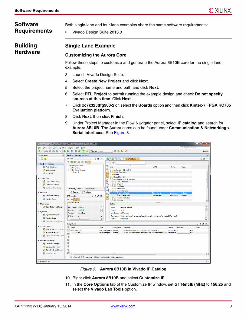
9. Under Project Manager in the Flow Navigator panel, select IP catalog and search for Aurora 8B10B. The Aurora cores can be found under Communication & Networking > Serial Interfaces. See Figure 3.
10. Right-click Aurora 8B10B and select Customize IP.
11. In the Core Options tab of the Customize IP window, set GT Refclk (MHz) to 156.25 and select the Vivado Lab Tools option.
X-Ref Target - Figure 3
Figure 3: Aurora 8B10B in Vivado IP Catalog

Building Hardware
XAPP1193 (v1.0) January 15, 2014 www.xilinx.com 4
12. Set the configuration options shown in Figure 4.
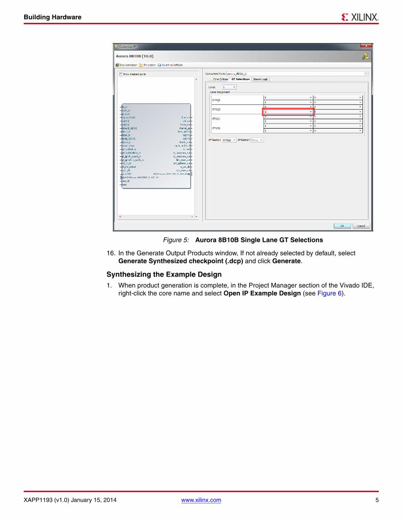
13. Click the GT Selections tab.
14. Change the default setting in the lower list box for GTXQ0 from 1 to X.
15. Change the lower list box setting for GTXQ2 from X to 1 (Figure 5) and click OK.
Note: The GTXQ2 transceiver is the only transceiver pinned out to SMA connectors on the KC705 board. When placing the cursor over the list box setting, a tooltip appears to verify the location of the selected transceiver.
X-Ref Target - Figure 4
Figure 4: Aurora 8B10B Single Lane Core Options Settings
Building Hardware
XAPP1193 (v1.0) January 15, 2014 www.xilinx.com 5
16. In the Generate Output Products window, If not already selected by default, select Generate Synthesized checkpoint (.dcp) and click Generate.
Synthesizing the Example Design1. When product generation is complete, in the Project Manager section of the Vivado IDE,
right-click the core name and select Open IP Example Design (see Figure 6).
X-Ref Target - Figure 5
Figure 5: Aurora 8B10B Single Lane GT Selections

Building Hardware
XAPP1193 (v1.0) January 15, 2014 www.xilinx.com 6
2. Click OK to overwrite the existing example design.
3. Click OK to acknowledge IP upgrade then click Generate to generate the 7 series ILA cores.
4. Click OK to acknowledge IP upgrade then click Generate to generate the 7 series VIO cores.
5. In the newly-opened Vivado IDE window, expand the Constraints entry in the Sources panel of the Project Manager section. Right-click the constraints file (aurora_8b10b_0_exdes.xdc) and select Open file (Figure 7).
6. Assign the pin locations for the Aurora core ports to those shown in Table 1.
X-Ref Target - Figure 6
Figure 6: Open IP Example Design

Building Hardware
XAPP1193 (v1.0) January 15, 2014 www.xilinx.com 7
7. This example contains unconstrained pins. To permit bitsream file generation, add this line to the end of the constraints file (Figure 7):
set_property BITSTREAM.General.UnconstrainedPins {Allow} [current_design]
Caution! Spelling is critical. Double-check changes to the constraints file before proceeding.
8. Right-click within the constraints file editor window and select Save File. Close the constraints file editor window.
9. Select Generate Bitstream from the Flow Navigator panel (Figure 8).
X-Ref Target - Figure 7
Figure 7: Aurora 8B10B Single Lane Constraints File
Table 1: Aurora 8B10B Single Lane Constraints
Pin Name LOC Value
GTXQ2_N J7
GTXQ2_P J8
INIT_CLK_N AD11
INIT_CLK_P AD12
RESET AG5
GT_RESET_IN AC6
CHANNEL_UP AA8
LANE_UP AB8
HARD_ERR G17
SOFT_ERR F17
ERR_COUNT B17

Building Hardware
XAPP1193 (v1.0) January 15, 2014 www.xilinx.com 8
10. Click Yes to launch Synthesis and Implementation and proceed with bitstream file generation.
Continue with Setting up the Single Lane Example, page 14.
Four Lane Example
Customizing the Aurora Core
Follow these steps to customize and generate the Aurora 8B10B core for the four lane example:
1. Launch Vivado Design Suite.
2. Select Create New Project and click Next.
3. Select the project name and path and click Next.
4. Select RTL Project to permit running the example design and check Do not specify sources at this time. Click Next.
5. Click xc7k325tffg900-2, or, select the Boards option and then click Kintex-7 FPGA KC705 Evaluation platform.
6. Click Next then click Finish.
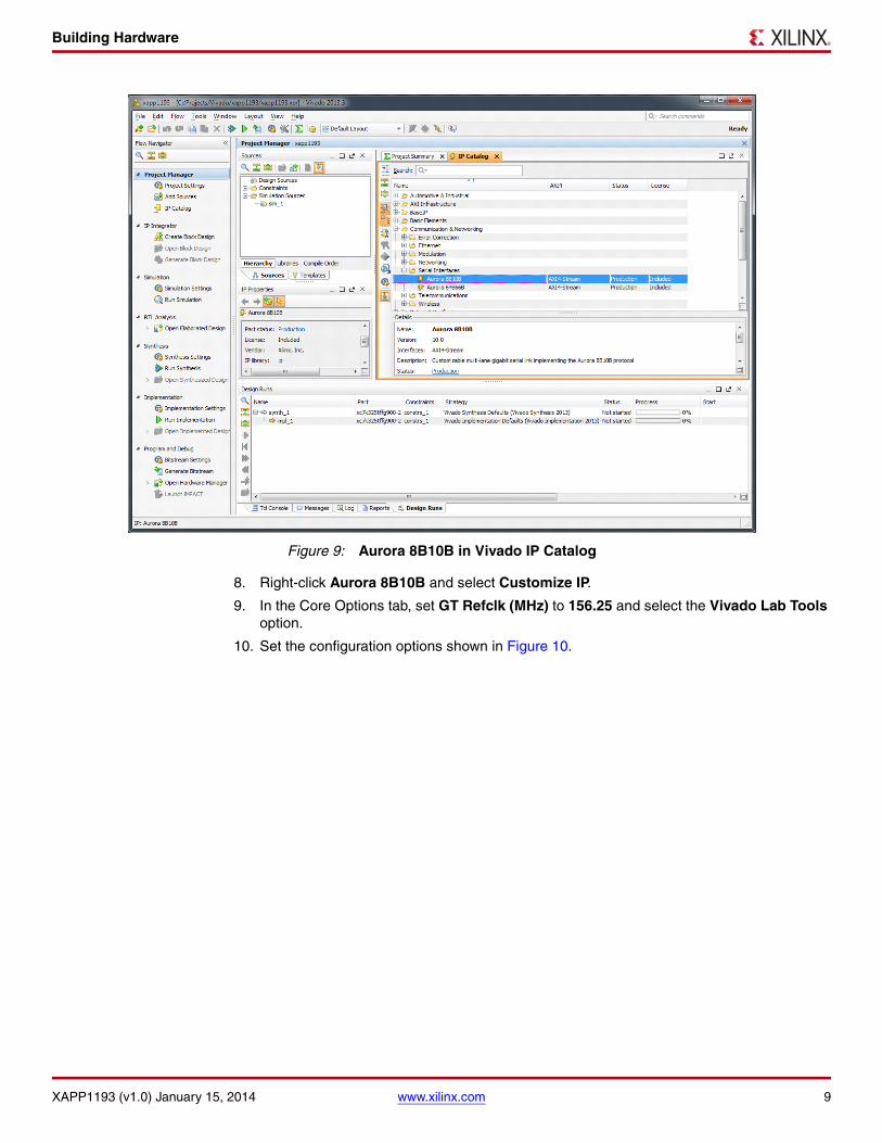
7. Under Project Manager in the Flow Navigator panel, select IP catalog and search for Aurora 8B10B. The Aurora cores can be found under Communication & Networking > Serial Interfaces. See Figure 9.
X-Ref Target - Figure 8
Figure 8: Generate Bitstream
Building Hardware
XAPP1193 (v1.0) January 15, 2014 www.xilinx.com 9
8. Right-click Aurora 8B10B and select Customize IP.
9. In the Core Options tab, set GT Refclk (MHz) to 156.25 and select the Vivado Lab Tools option.
10. Set the configuration options shown in Figure 10.
X-Ref Target - Figure 9
Figure 9: Aurora 8B10B in Vivado IP Catalog

Building Hardware
XAPP1193 (v1.0) January 15, 2014 www.xilinx.com 10
11. Click the GT Selections tab.
12. Set Lanes to 4.
13. Change the default setting in the lower left list box for GTXQ0 from 1 to X.
14. Change the list box settings for GTXQ2 from X to 1, 2, 3, and 4 (see Figure 11) and click OK.
Note: The GTXQ2 transceiver is the only transceiver pinned out to SMA connectors on the KC705 board. When placing the cursor over the list box setting, a tooltip appears to verify the location of the selected transceiver.
X-Ref Target - Figure 10
Figure 10: Aurora 8B10B Four Lane Core Options Settings

Building Hardware
XAPP1193 (v1.0) January 15, 2014 www.xilinx.com 11
15. In the Generate Output Products window, if not already selected by default, select Generate Synthesized checkpoint (.dcp) and click Generate.
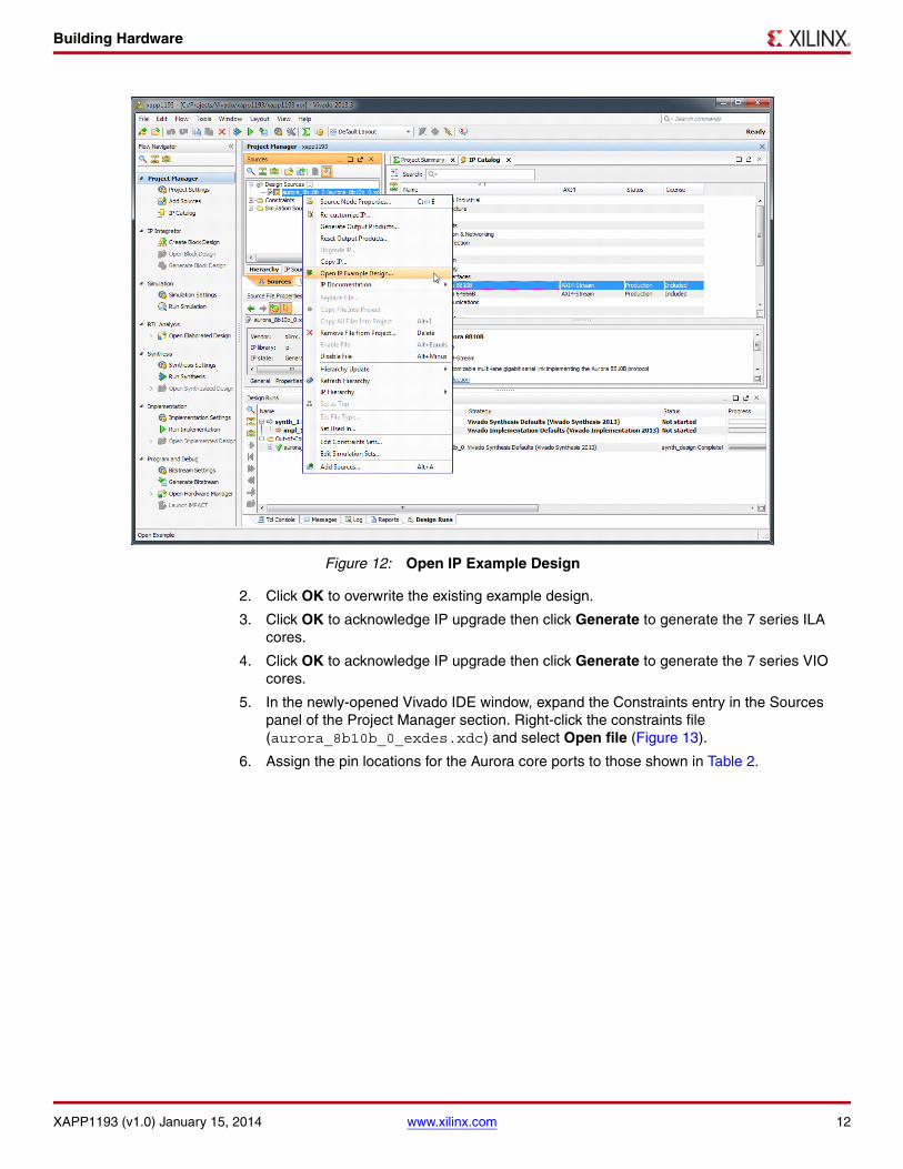
Synthesizing the Aurora Core1. When product generation is complete, in the Project Manager section of the Vivado IDE,
right-click the core name and select Open IP Example Design (Figure 12).
X-Ref Target - Figure 11
Figure 11: Aurora 8B10B Four Lane GT Selections
Building Hardware
XAPP1193 (v1.0) January 15, 2014 www.xilinx.com 12
2. Click OK to overwrite the existing example design.
3. Click OK to acknowledge IP upgrade then click Generate to generate the 7 series ILA cores.
4. Click OK to acknowledge IP upgrade then click Generate to generate the 7 series VIO cores.
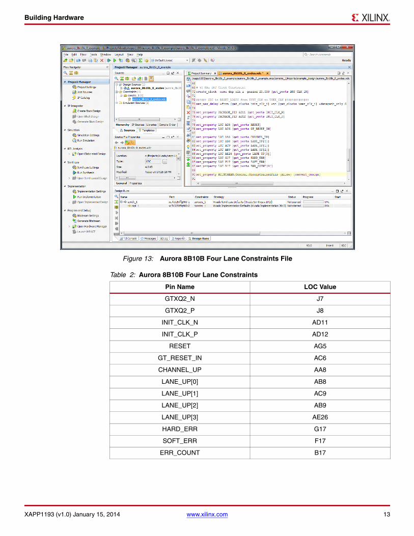
5. In the newly-opened Vivado IDE window, expand the Constraints entry in the Sources panel of the Project Manager section. Right-click the constraints file (aurora_8b10b_0_exdes.xdc) and select Open file (Figure 13).
6. Assign the pin locations for the Aurora core ports to those shown in Table 2.
X-Ref Target - Figure 12
Figure 12: Open IP Example Design
Building Hardware
XAPP1193 (v1.0) January 15, 2014 www.xilinx.com 13
X-Ref Target - Figure 13
Figure 13: Aurora 8B10B Four Lane Constraints File
Table 2: Aurora 8B10B Four Lane Constraints
Pin Name LOC Value
GTXQ2_N J7
GTXQ2_P J8
INIT_CLK_N AD11
INIT_CLK_P AD12
RESET AG5
GT_RESET_IN AC6
CHANNEL_UP AA8
LANE_UP[0] AB8
LANE_UP[1] AC9
LANE_UP[2] AB9
LANE_UP[3] AE26
HARD_ERR G17
SOFT_ERR F17
ERR_COUNT B17

Executing the Reference Design in Hardware
XAPP1193 (v1.0) January 15, 2014 www.xilinx.com 14
7. This example contains unconstrained pins. To permit bitsream file generation, add this line to the end of the constraints file (Figure 13):
set_property BITSTREAM.General.UnconstrainedPins {Allow} [current_design]
Caution! Spelling is critical. Double-check changes to the constraints file before proceeding.
8. Right-click within the constraints file window and select Save File. Close the window.
9. Select Generate Bitstream from the Flow Navigator panel (Figure 14).
10. Click Yes to launch Synthesis and Implementation and proceed with bitstream file generation.
Continue with Setting Up the Four Lane Example, page 16.
Executing the Reference Design in Hardware
Setting up the Single Lane Example
This example illustrates a single lane Aurora 8B10B connection between two platforms (see Figure 1, page 2). The platforms consist of two Kintex-7 FPGA KC705 Evaluation Kit boards shown in Figure 15.
X-Ref Target - Figure 14
Figure 14: Generate Bitstream

Executing the Reference Design in Hardware
XAPP1193 (v1.0) January 15, 2014 www.xilinx.com 15
In these instructions, numbers in parentheses correspond to callout numbers in Figure 15. Make these connections using the SMA to SMA connector cables.
1. Connect TXP from board 1 (4) to RXP of board 2 (5).
2. Connect TXN from board 1 (7) to RXN of board 2 (6).
3. Connect TXP from board 2 (4) to RXP of board 1 (5).
4. Connect TXN from board 2 (7) to RXN of board 1 (6).
5. Connect CLKP from clock source 1 to MGT CLK P of board 1 (2).
6. Connect CLKN from clock source 1 to MGT CLK N of board 1 (3).
7. Connect CLKP from clock source 2 to MGT CLK P of board 2 (2).
8. Connect CLKN from clock source 2 to MGT CLK N of board 2 (3).
9. Connect a JTAG platform USB cable from the host PC to the platform cable header of board 1 (1).
10. Connect a JTAG platform USB cable from the host PC to the platform cable header of board 2 (1).
11. Connect a KC705 Universal 12v power adapter cable to the power connector (9) of both boards.
12. Set the power switch (8) of both boards to the ON position.
The completed setup should resemble that shown in Figure 16.
Note: Separate clock sources should be used for each board.
X-Ref Target - Figure 15
Figure 15: KC705 Board Features
52
1
9
8
3
4
6
7

Executing the Reference Design in Hardware
XAPP1193 (v1.0) January 15, 2014 www.xilinx.com 16
Continue with Setting Up the Single Lane Hardware Session, page 17.
Setting Up the Four Lane Example
This example illustrates a four lane Aurora 8B10B connection on one platform using internal loopback (see Figure 2, page 2). The platform consists of one Kintex-7 FPGA KC705 Evaluation Kit board shown in Figure 15, page 15.
In these instructions, numbers in parentheses correspond to callout numbers in Figure 15. Make these connections using the SMA to SMA connector cables.
1. Connect CLKP from the clock source to MGT CLK P of the platform board (2).
2. Connect CLKN from the clock source to MGT CLK N of the platform board (3).
3. Connect a KC705 Universal 12v power adapter cable to the power connector (9).
4. Set the power switch (8) to the ON position.
The completed setup should resemble that shown in Figure 17.
X-Ref Target - Figure 16
Figure 16: Aurora 8B10B Single Lane Setup
Clock Source 1 Clock Source 2

Executing the Reference Design in Hardware
XAPP1193 (v1.0) January 15, 2014 www.xilinx.com 17
Continue with Setting Up the Four Lane Hardware Session, page 23.
Setting Up the Single Lane Hardware Session
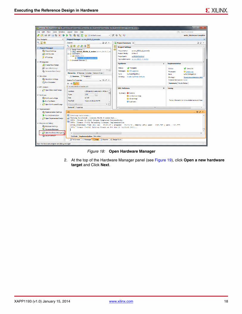
Programming the Devices1. Under Program and Debug in the Project Manager section of the Vivado IDE, click Open
Hardware Manager (Figure 18).
X-Ref Target - Figure 17
Figure 17: Aurora 8B10B Four Lane Setup
Clock Source
Executing the Reference Design in Hardware
XAPP1193 (v1.0) January 15, 2014 www.xilinx.com 18
2. At the top of the Hardware Manager panel (see Figure 19), click Open a new hardware target and Click Next.
X-Ref Target - Figure 18
Figure 18: Open Hardware Manager

Executing the Reference Design in Hardware
XAPP1193 (v1.0) January 15, 2014 www.xilinx.com 19
3. Leave the Server name <host[:port]> set to localhost:60001 and click Next.
Note: This operation assumes the hardware target is connected to the host PC running Vivado Design Suite. It is possible to connect the hardware target to a second, networked host PC using the Vivado CSE Server application. For details, see the Using a Vivado Hardware Manager to Program an FPGA Device section in Vivado Design Suite User Guide: Programming and Debugging (UG908), [Ref 3].
4. Click to highlight one of the platform boards in the Hardware Targets list and click Next, then click Finish.
5. In the Hardware panel, click the active device, XC7K325T_0(0) (Active).
6. In the Hardware Device Properties panel, set Programming file to the bitstream file name (aurora_8b10b_0_exdes.bit) and set Probes file to the probes file name (debug_nets.ltx, Figure 20).
X-Ref Target - Figure 19
Figure 19: Open a New Hardware Target
X-Ref Target - Figure 20
Figure 20: Hardware Device Properties

Executing the Reference Design in Hardware
XAPP1193 (v1.0) January 15, 2014 www.xilinx.com 20
7. Right-click the device in the Hardware list and select Program Device... (Figure 21). Ensure that the bitstream file path and name are correct and click OK.
8. When programming completes, right-click the programmed target device in the Hardware list and select Close Target (Figure 22).
9. Right-click the second target platform in the Hardware list and select Open Target (Figure 23).
10. Repeat step 6 and step 7 using the same bitstream and probes file names that were used for the first target.
11. When programming completes, right-click the programmed target device in the Hardware list and select Refresh Device (Figure 24).
X-Ref Target - Figure 21
Figure 21: Program Device
X-Ref Target - Figure 22
Figure 22: Close Target
X-Ref Target - Figure 23
Figure 23: Open Target

Executing the Reference Design in Hardware
XAPP1193 (v1.0) January 15, 2014 www.xilinx.com 21
Executing the Design
1. Right-click the device in the Hardware list and select Run Trigger. In the waveform window that appears, observe a High state on the lane_up and channel_up signals (see Figure 25).
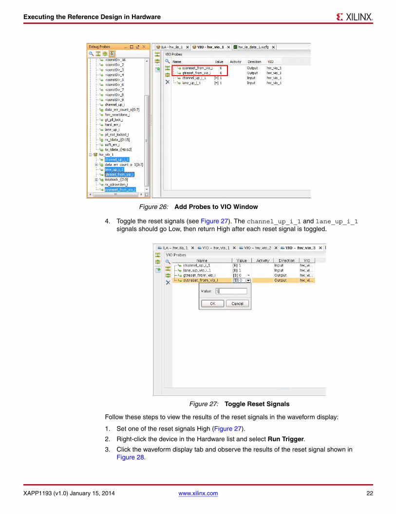
2. Control-click to select these signals in the Debug Probes list under hw_vio_1:
• channel_up_i_1
• lane_up_i_1
• gtreset_from_vio_i
• sysreset_from_vio_i
3. Right-click the selection and select Add Probes to VIO Window (Figure 26).
X-Ref Target - Figure 24
Figure 24: Refresh Device
X-Ref Target - Figure 25
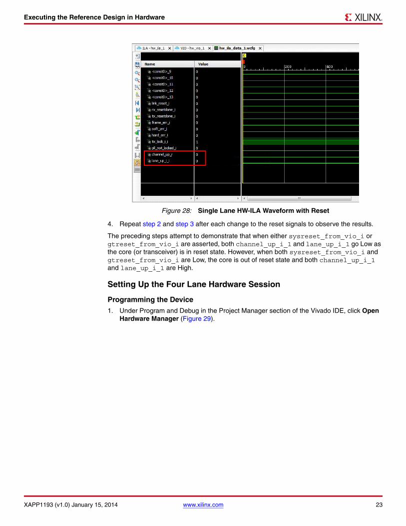
Figure 25: Single Lane HW-ILA Waveform
Executing the Reference Design in Hardware
XAPP1193 (v1.0) January 15, 2014 www.xilinx.com 22
4. Toggle the reset signals (see Figure 27). The channel_up_i_1 and lane_up_i_1 signals should go Low, then return High after each reset signal is toggled.
Follow these steps to view the results of the reset signals in the waveform display:
1. Set one of the reset signals High (Figure 27).
2. Right-click the device in the Hardware list and select Run Trigger.
3. Click the waveform display tab and observe the results of the reset signal shown in Figure 28.
X-Ref Target - Figure 26
Figure 26: Add Probes to VIO Window
X-Ref Target - Figure 27
Figure 27: Toggle Reset Signals
Executing the Reference Design in Hardware
XAPP1193 (v1.0) January 15, 2014 www.xilinx.com 23
4. Repeat step 2 and step 3 after each change to the reset signals to observe the results.
The preceding steps attempt to demonstrate that when either sysreset_from_vio_i or gtreset_from_vio_i are asserted, both channel_up_i_1 and lane_up_i_1 go Low as the core (or transceiver) is in reset state. However, when both sysreset_from_vio_i and gtreset_from_vio_i are Low, the core is out of reset state and both channel_up_i_1 and lane_up_i_1 are High.
Setting Up the Four Lane Hardware Session
Programming the Device1. Under Program and Debug in the Project Manager section of the Vivado IDE, click Open
Hardware Manager (Figure 29).
X-Ref Target - Figure 28
Figure 28: Single Lane HW-ILA Waveform with Reset

Executing the Reference Design in Hardware
XAPP1193 (v1.0) January 15, 2014 www.xilinx.com 24
2. At the top of the Hardware Manager panel, click Open a new hardware target (Figure 30) and click Next.
X-Ref Target - Figure 29
Figure 29: Open Hardware Manager

Executing the Reference Design in Hardware
XAPP1193 (v1.0) January 15, 2014 www.xilinx.com 25
3. Leave the Server name <host[:port]> set to local host:60001 and click Next.
Note: This operation assumes the hardware target is connected to the host PC running Vivado Design Suite. It is possible to connect the hardware target to a second, networked host PC using the Vivado CSE Server application. For details, see the Using a Vivado Hardware Manager to Program an FPGA Device section in Vivado Design Suite User Guide: Programming and Debugging (UG908), [Ref 3].
4. Click to highlight one of the platform boards in the Hardware Targets list and click Next, then click Finish.
5. In the Hardware panel, click the active device, XC7K325T_0(0) (Active).
6. In the Hardware Device Properties panel, set Programming file to the bitstream file name (aurora_8b10b_0_exdes.bit) and set Probes file to the probes file name (debug_nets.ltx, Figure 31).
X-Ref Target - Figure 30
Figure 30: Open a New Hardware Target
X-Ref Target - Figure 31
Figure 31: Hardware Device Properties
Executing the Reference Design in Hardware
XAPP1193 (v1.0) January 15, 2014 www.xilinx.com 26
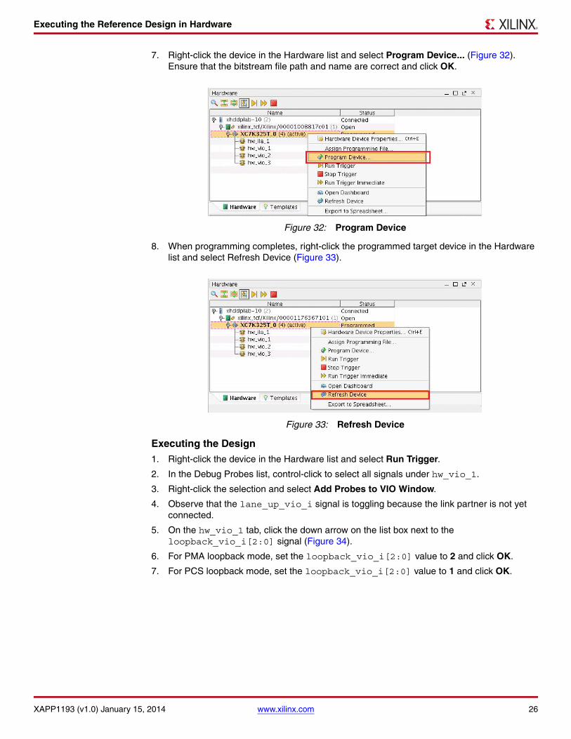
7. Right-click the device in the Hardware list and select Program Device... (Figure 32). Ensure that the bitstream file path and name are correct and click OK.
8. When programming completes, right-click the programmed target device in the Hardware list and select Refresh Device (Figure 33).
Executing the Design1. Right-click the device in the Hardware list and select Run Trigger.
2. In the Debug Probes list, control-click to select all signals under hw_vio_1.
3. Right-click the selection and select Add Probes to VIO Window.
4. Observe that the lane_up_vio_i signal is toggling because the link partner is not yet connected.
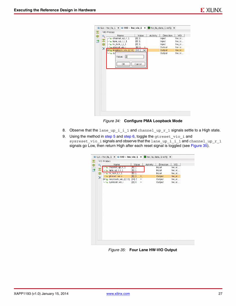
5. On the hw_vio_1 tab, click the down arrow on the list box next to the loopback_vio_i[2:0] signal (Figure 34).
6. For PMA loopback mode, set the loopback_vio_i[2:0] value to 2 and click OK.
7. For PCS loopback mode, set the loopback_vio_i[2:0] value to 1 and click OK.
X-Ref Target - Figure 32
Figure 32: Program Device
X-Ref Target - Figure 33
Figure 33: Refresh Device
Executing the Reference Design in Hardware
XAPP1193 (v1.0) January 15, 2014 www.xilinx.com 27
8. Observe that the lane_up_i_i_1 and channel_up_r_1 signals settle to a High state.
9. Using the method in step 5 and step 6, toggle the gtreset_vio_i and sysreset_vio_i signals and observe that the lane_up_i_i_1 and channel_up_r_1 signals go Low, then return High after each reset signal is toggled (see Figure 35).
X-Ref Target - Figure 34
Figure 34: Configure PMA Loopback Mode
X-Ref Target - Figure 35
Figure 35: Four Lane HW-VIO Output

Reference Design
XAPP1193 (v1.0) January 15, 2014 www.xilinx.com 28
Follow these steps to view the results of the reset signals in the waveform display:
1. Using the method described previously in step 5 and step 6, set gt_reset_vio_i and sysreset_vio_i Low.
2. Right-click the device in the Hardware list and select Run Trigger.
3. Click the waveform display tab and observe the results of the reset signal shown in Figure 36.
4. Repeat step 2 and step 3 after each change to the reset signals to observe the results.
The preceding steps attempt to demonstrate that when either sysreset_vio_i or gtreset_vio_i are asserted, both channel_up_r_1 and lane_up_i_i_1 go Low as the core (or transceiver) is in reset state. However, when both sysreset_vio_i and gtreset_vio_i are Low, the core is out of reset state and both channel_up_r_1 and lane_up_i_i_1 are High.
Reference Design
The reference design files for this application note are generated when the Aurora 8B10B core is customized from the Vivado IP catalog.
Table 3 shows the reference design checklist.
X-Ref Target - Figure 36
Figure 36: Four Lane HW-ILA Waveform with Reset
Table 3: Reference Design Checklist
Parameter Description
General
Developer name Dinesh Kumar, Ramachandra Thupalli
Target devices (stepping level, ES, production, speed grades)
Kintex-7 XC7K325T-2FFG900
Source code provided Yes
Source code format Verilog (VHDL indirect support through vho/netlist)

Conclusion
XAPP1193 (v1.0) January 15, 2014 www.xilinx.com 29
Conclusion The Kintex-7 FPGA KC705 Evaluation Kit provides an excellent platform to implement and test the LogiCORE IP Aurora 8B10B core. Various configurations can be quickly evaluated using only the KC705 board, a clock source and the Vivado Design Suite.
References Refer to these documents for additional details:
1. LogiCORE IP Aurora 8B/10B Product Guide (PG046)
2. Vivado Design Suite User Guide: Designing with IP (UG896)
3. Vivado Design Suite User Guide: Programming and Debugging (UG908)
Revision History
The following table shows the revision history for this document.
Design uses code/IP from existing Xilinx application note/reference designs, CORE Generator™ software, or third party
Reference design provided by Aurora core generated from Vivado IP catalog
Simulation
Functional simulation performed No
Timing simulation performed No
Test bench used for functional and timing simulations
N/A
Test bench format N/A
Simulator software/version used N/A
SPICE/IBIS simulations No
Implementation
Synthesis software tools/version used Vivado Design Suite 2013.3
Implementation software tools/versions used Vivado Design Suite 2013.3
Static timing analysis performed Yes (passing timing in PAR/TRCE)
Hardware Verification
Hardware verified Yes
Hardware platform used for verification Kintex-7 FPGA KC705 evaluation kit
Table 3: Reference Design Checklist (Cont’d)
Parameter Description
Date Version Description of Revisions
01/15/2014 1.0 Initial Xilinx release.

Notice of Disclaimer
XAPP1193 (v1.0) January 15, 2014 www.xilinx.com 30
Notice of Disclaimer
The information disclosed to you hereunder (the “Materials”) is provided solely for the selection and use ofXilinx products. To the maximum extent permitted by applicable law: (1) Materials are made available "ASIS" and with all faults, Xilinx hereby DISCLAIMS ALL WARRANTIES AND CONDITIONS, EXPRESS,IMPLIED, OR STATUTORY, INCLUDING BUT NOT LIMITED TO WARRANTIES OFMERCHANTABILITY, NON-INFRINGEMENT, OR FITNESS FOR ANY PARTICULAR PURPOSE; and (2)Xilinx shall not be liable (whether in contract or tort, including negligence, or under any other theory ofliability) for any loss or damage of any kind or nature related to, arising under, or in connection with, theMaterials (including your use of the Materials), including for any direct, indirect, special, incidental, orconsequential loss or damage (including loss of data, profits, goodwill, or any type of loss or damagesuffered as a result of any action brought by a third party) even if such damage or loss was reasonablyforeseeable or Xilinx had been advised of the possibility of the same. Xilinx assumes no obligation tocorrect any errors contained in the Materials or to notify you of updates to the Materials or to productspecifications. You may not reproduce, modify, distribute, or publicly display the Materials without priorwritten consent. Certain products are subject to the terms and conditions of the Limited Warranties whichcan be viewed at http://www.xilinx.com/warranty.htm; IP cores may be subject to warranty and supportterms contained in a license issued to you by Xilinx. Xilinx products are not designed or intended to befail-safe or for use in any application requiring fail-safe performance; you assume sole risk and liability foruse of Xilinx products in Critical Applications: http://www.xilinx.com/warranty.htm#critapps.
Automotive Applications Disclaimer
XILINX PRODUCTS ARE NOT DESIGNED OR INTENDED TO BE FAIL-SAFE, OR FOR USE IN ANY APPLICATION REQUIRING FAIL-SAFE PERFORMANCE, SUCH AS APPLICATIONS RELATED TO: (I) THE DEPLOYMENT OF AIRBAGS, (II) CONTROL OF A VEHICLE, UNLESS THERE IS A FAIL-SAFE OR REDUNDANCY FEATURE (WHICH DOES NOT INCLUDE USE OF SOFTWARE IN THE XILINX DEVICE TO IMPLEMENT THE REDUNDANCY) AND A WARNING SIGNAL UPON FAILURE TO THE OPERATOR, OR (III) USES THAT COULD LEAD TO DEATH OR PERSONAL INJURY. CUSTOMER ASSUMES THE SOLE RISK AND LIABILITY OF ANY USE OF XILINX PRODUCTS IN SUCH APPLICATIONS.