Xilinx UG406 Virtex-6 FPGA Memory Interface Solutions, User Guide

Virtex-5 Libraries Guide forSchematic Designs
UG622 (v 13.1) March 1, 2011
Xilinx is disclosing this user guide, manual, release note, and/or specification (the “Documentation”) to yousolely for use in the development of designs to operate with Xilinx hardware devices. You may not reproduce,distribute, republish, download, display, post, or transmit the Documentation in any form or by any meansincluding, but not limited to, electronic, mechanical, photocopying, recording, or otherwise, without the priorwritten consent of Xilinx. Xilinx expressly disclaims any liability arising out of your use of the Documentation.Xilinx reserves the right, at its sole discretion, to change the Documentation without notice at any time. Xilinxassumes no obligation to correct any errors contained in the Documentation, or to advise you of any correctionsor updates. Xilinx expressly disclaims any liability in connection with technical support or assistance that may beprovided to you in connection with the Information.
THE DOCUMENTATION IS DISCLOSED TO YOU “AS-IS” WITH NOWARRANTY OF ANY KIND. XILINXMAKES NO OTHER WARRANTIES, WHETHER EXPRESS, IMPLIED, OR STATUTORY, REGARDINGTHE DOCUMENTATION, INCLUDING ANY WARRANTIES OF MERCHANTABILITY, FITNESS FOR APARTICULAR PURPOSE, OR NONINFRINGEMENT OF THIRD-PARTY RIGHTS. IN NO EVENT WILLXILINX BE LIABLE FOR ANY CONSEQUENTIAL, INDIRECT, EXEMPLARY, SPECIAL, OR INCIDENTALDAMAGES, INCLUDING ANY LOSS OF DATA OR LOST PROFITS, ARISING FROM YOUR USE OF THEDOCUMENTATION.
© Copyright 2002-2011 Xilinx Inc. All Rights Reserved. XILINX, the Xilinx logo, the Brand Window and otherdesignated brands included herein are trademarks of Xilinx, Inc. All other trademarks are the property oftheir respective owners.
Virtex-5 Libraries Guide for Schematic Designs2 www.xilinx.com UG622 (v 13.1) March 1, 2011
Chapter 1
IntroductionThis schematic guide is part of the ISE documentation collection. A separate version ofthis guide is available if you prefer to work with HDL.
This guide contains the following:
• Introduction.
• A list of retargeted elements.
• A list of design elements supported in this architecture, organized by functionalcategories.
• Detailed descriptions of each available macro.
• Individual descriptions of each available primitive.
About Design ElementsThis version of the Libraries Guide describes design elements available for thisarchitecture. There are several categories of design elements:
• Retargeted Elements - These elements are automatically changed by the ISEsoftware tools when they are used in this architecture. Retargeting ensures that yourdesign takes advantage of the latest circuit design advances.
• Primitives - The simplest design elements in the Xilinx libraries. Primitives are thedesign element "atoms." Examples of Xilinx primitives are the simple buffer, BUF,and the D flip-flop with clock enable and clear, FDCE.
• Macros - The design element "molecules" of the Xilinx libraries. Macros can becreated from the design element primitives or macros. For example, the FD4CEflip-flop macro is a composite of 4 FDCE primitives.
Xilinx maintains software libraries with hundreds of functional design elements(macros and primitives) for different device architectures. New functional elements areassembled with each release of development system software. This guide is one ina series of architecture-specific libraries.
Virtex-5 Libraries Guide for Schematic DesignsUG622 (v 13.1) March 1, 2011 www.xilinx.com 3

Virtex-5 Libraries Guide for Schematic Designs4 www.xilinx.com UG622 (v 13.1) March 1, 2011

Chapter 2
Design Element RetargetingTo ensure that Xilinx® customers are able to take full advantage of the latest circuitdesign advances, certain design elements are automatically changed by the ISE® DesignSuite software tools when they are used in this architecture.
The following table lists these elements and the more advanced elements into whichthey are transformed.
Original Element Modern EquivalentBUFGCE_1 BUFGCE + INV
BUFGMUX BUFGMUX_CTRL
BUFGMUX_1 BUFGMUX_CTRL + INV
BUFGMUX_VIRTEX4 BUFGMUX_CTRL
BUFGP BUFG
DCM_BASE DCM_ADV
DCM_PS DCM_ADV
DSP48 DSP48E
FD FDCPE
FD_1 FDCPE + INV
FDC FDCPE
FDC_1 FDCPE + INV
FDCE FDCPE
FDCE_1 FDCPE + INV
FDCP FDCPE
FDCP_1 FDCPE + INV
FDE FDCPE
FDE_1 FDCPE + INV
FDPE FDCPE
FDPE_1 FDCPE + INV
FDR FDRSE
FDR_1 FDRSE + INV
FDRE FDRSE
FDRE_1 FDRSE + INV
FDRS FDRSE
Virtex-5 Libraries Guide for Schematic DesignsUG622 (v 13.1) March 1, 2011 www.xilinx.com 5

Chapter 2: Design Element Retargeting
Original Element Modern EquivalentFDRS_1 FDRSE + INV
FDS FDRSE
FDS_1 FDRSE + INV
FDSE FDRSE
FDSE_1 FDRSE + INV
FIFO16 FIFO18
ISERDES ISERDES_NODELAY
JTAGPPC JTAG_PPC440
LD LDCPE
LD_1 LDCPE + INV
LDC LDCPE
LDC_1 LDCPE + INV
LDCE LDCPE
LDCE_1 LDCPE + INV
LDCP LDCPE
LDCP_1 LDCPE + INV
LDE LDCPE
LDE_1 LDCPE + INV
LDP LDCPE
LDP_1 LDCPE + INV
LDPE LDCPE
LDPE_1 LDCPE + INV
LUT1 LUT5
LUT1_L LUT5_L
LUT1_D LUT5_D
LUT2 LUT5
LUT2_L LUT5_L
LUT2_D LUT5_D
LUT3 LUT5
LUT3_L LUT5_L
LUT3_D LUT5_D
LUT4 LUT5
LUT4_L LUT5_L
LUT4_D LUT5_D
MULT_AND LUT6
MULT18X18 DSP48E
MULT18X18S DSP48E
MUXCY CARRY4
Virtex-5 Libraries Guide for Schematic Designs6 www.xilinx.com UG622 (v 13.1) March 1, 2011

Chapter 2: Design Element Retargeting
Original Element Modern EquivalentMUXCY_D CARRY4
MUXCY_L CARRY4
MUXF5 LUT5
MUXF5_D LUT5_D
MUXF5_L LUT5_L
MUXF6 LUT6
MUXF6_D LUT6_D
MUXF6_L LUT6_L
PMCD PLL_ADV
RAM16X1D RAM64X1D
RAM16X1S RAM64X1S
RAM32X1S RAM64X1S
RAMB16 RAMB18
RAMB16BWE RAMB18
ROM128X1 2 LUT6’S + MUXF7
ROM16X1 LUT5
ROM256X1 4 LUT6’S + MUXF6/7
ROM32X1 LUT5
ROM64X1 LUT6
SRLC16 SRLC32E
SRLC16_1 SRLC32E + INV
SRLC16E SRLC32E
SRLC16E_1 SRLC32E + INV
XORCY CARRY4
XORCY_D CARRY4
XORCY_L CARRY4
Virtex-5 Libraries Guide for Schematic DesignsUG622 (v 13.1) March 1, 2011 www.xilinx.com 7

Virtex-5 Libraries Guide for Schematic Designs8 www.xilinx.com UG622 (v 13.1) March 1, 2011

Chapter 3
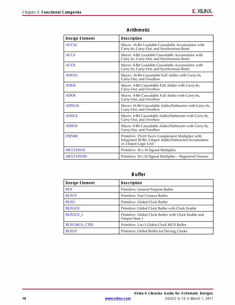
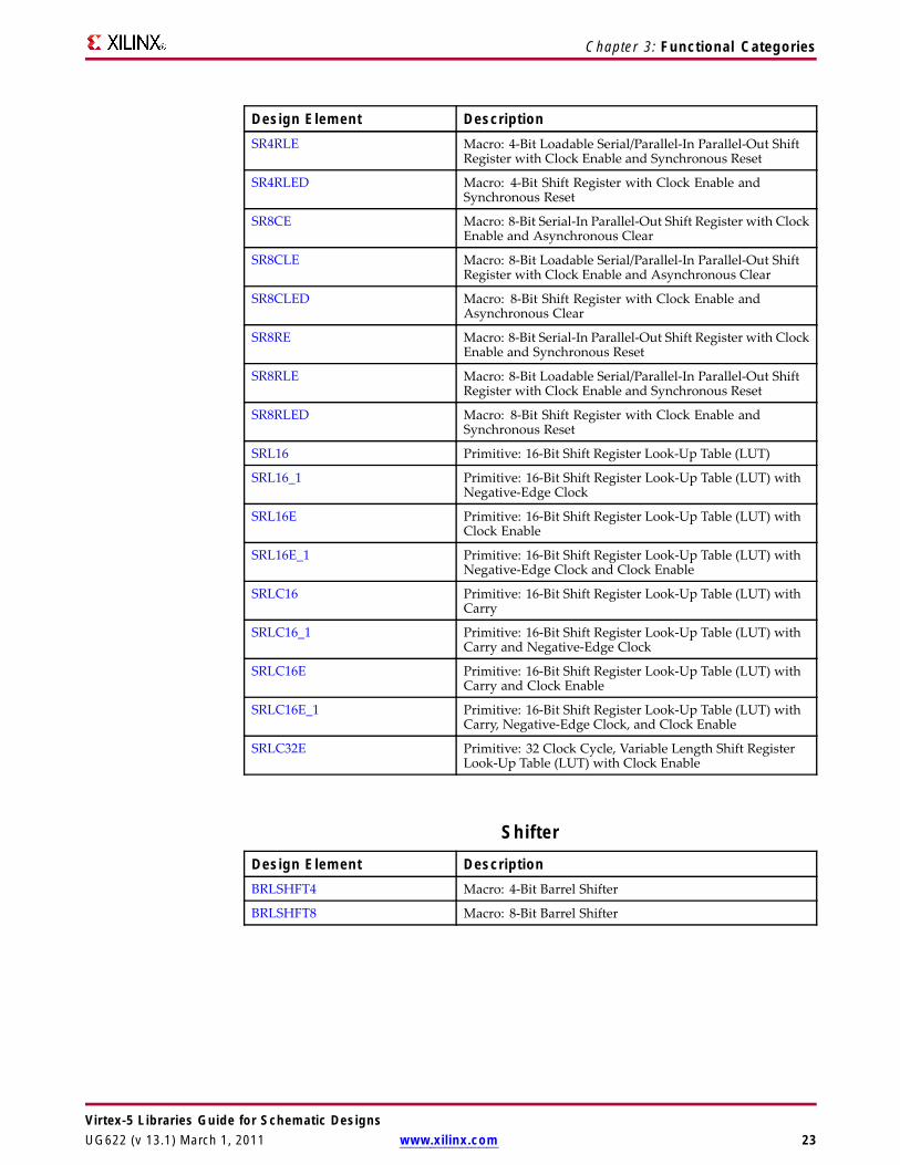
Functional CategoriesThis section categorizes, by function, the circuit design elements described in detail laterin this guide. The elements ( primitives and macros) are listed in alphanumeric orderunder each functional category.
Advanced Flip Flop Logic
Arithmetic General LUT
Buffer GigaBit IO/Processor Memory
Carry Logic Input/Output Functions Mux
Clocking Resources IO Shift Register
Comparator IO FlipFlop Shifter
Counter IO Latch
Decoder Latch
AdvancedDesign Element DescriptionCRC32 Primitive: Cyclic Redundancy Check Calculator for 32 bits
CRC64 Primitive: Cyclic Redundancy Check Calculator for 64 bits
GTP_DUAL Primitive: Dual Gigabit Transceiver
GTX_DUAL Primitive: Dual Gigabit Transceiver
PCIE_EP Primitive: PCI Express
TEMAC Primitive: Tri-mode Ethernet Media Access Controller(MAC)
Virtex-5 Libraries Guide for Schematic DesignsUG622 (v 13.1) March 1, 2011 www.xilinx.com 9
Chapter 3: Functional Categories
ArithmeticDesign Element DescriptionACC16 Macro: 16-Bit Loadable Cascadable Accumulator with
Carry-In, Carry-Out, and Synchronous Reset
ACC4 Macro: 4-Bit Loadable Cascadable Accumulator withCarry-In, Carry-Out, and Synchronous Reset
ACC8 Macro: 8-Bit Loadable Cascadable Accumulator withCarry-In, Carry-Out, and Synchronous Reset
ADD16 Macro: 16-Bit Cascadable Full Adder with Carry-In,Carry-Out, and Overflow
ADD4 Macro: 4-Bit Cascadable Full Adder with Carry-In,Carry-Out, and Overflow
ADD8 Macro: 8-Bit Cascadable Full Adder with Carry-In,Carry-Out, and Overflow
ADSU16 Macro: 16-Bit Cascadable Adder/Subtracter with Carry-In,Carry-Out, and Overflow
ADSU4 Macro: 4-Bit Cascadable Adder/Subtracter with Carry-In,Carry-Out, and Overflow
ADSU8 Macro: 8-Bit Cascadable Adder/Subtracter with Carry-In,Carry-Out, and Overflow
DSP48E Primitive: 25x18 Two’s Complement Multiplier withIntegrated 48-Bit, 3-Input Adder/Subtracter/Accumulatoror 2-Input Logic Unit
MULT18X18 Primitive: 18 x 18 Signed Multiplier
MULT18X18S Primitive: 18 x 18 Signed Multiplier -- Registered Version
BufferDesign Element DescriptionBUF Primitive: General Purpose Buffer
BUFCF Primitive: Fast Connect Buffer
BUFG Primitive: Global Clock Buffer
BUFGCE Primitive: Global Clock Buffer with Clock Enable
BUFGCE_1 Primitive: Global Clock Buffer with Clock Enable andOutput State 1
BUFGMUX_CTRL Primitive: 2-to-1 Global Clock MUX Buffer
BUFGP Primitive: Global Buffer for Driving Clocks
Virtex-5 Libraries Guide for Schematic Designs10 www.xilinx.com UG622 (v 13.1) March 1, 2011

Chapter 3: Functional Categories
Carry LogicDesign Element DescriptionCARRY4 Primitive: Fast Carry Logic with Look Ahead
MUXCY Primitive: 2-to-1 Multiplexer for Carry Logic with GeneralOutput
MUXCY_D Primitive: 2-to-1 Multiplexer for Carry Logic with DualOutput
MUXCY_L Primitive: 2-to-1 Multiplexer for Carry Logic with LocalOutput
XORCY Primitive: XOR for Carry Logic with General Output
Clocking ResourcesDesign Element DescriptionBUFGCTRL Primitive: Global Clock MUX Buffer
BUFIO Primitive: Local Clock Buffer for I/O
BUFR Primitive: Regional Clock Buffer for I/O and LogicResources
DCM_ADV Primitive: Advanced Digital Clock Manager Circuit
DCM_BASE Primitive: Base Digital Clock Manager Circuit
DCM_PS Primitive: Digital Clock Manager with Basic and PhaseShift Features
PLL_ADV Primitive: Advanced Phase Locked Loop Clock Circuit
PLL_BASE Primitive: Basic Phase Locked Loop Clock Circuit
SYSMON Primitive: System Monitor
ComparatorDesign Element DescriptionCOMP16 Macro: 16-Bit Identity Comparator
COMP2 Macro: 2-Bit Identity Comparator
COMP4 Macro: 4-Bit Identity Comparator
COMP8 Macro: 8-Bit Identity Comparator
COMPM16 Macro: 16-Bit Magnitude Comparator
COMPM2 Macro: 2-Bit Magnitude Comparator
COMPM4 Macro: 4-Bit Magnitude Comparator
COMPM8 Macro: 8-Bit Magnitude Comparator
COMPMC16 Macro: 16-Bit Magnitude Comparator
COMPMC8 Macro: 8-Bit Magnitude Comparator
Virtex-5 Libraries Guide for Schematic DesignsUG622 (v 13.1) March 1, 2011 www.xilinx.com 11

Chapter 3: Functional Categories
CounterDesign Element DescriptionCB16CE Macro: 16-Bit Cascadable Binary Counter with Clock
Enable and Asynchronous Clear
CB16CLE Macro: 16-Bit Loadable Cascadable Binary Counters withClock Enable and Asynchronous Clear
CB16CLED Macro: 16-Bit Loadable Cascadable Bidirectional BinaryCounters with Clock Enable and Asynchronous Clear
CB16RE Macro: 16-Bit Cascadable Binary Counter with ClockEnable and Synchronous Reset
CB2CE Macro: 2-Bit Cascadable Binary Counter with Clock Enableand Asynchronous Clear
CB2CLE Macro: 2-Bit Loadable Cascadable Binary Counters withClock Enable and Asynchronous Clear
CB2CLED Macro: 2-Bit Loadable Cascadable Bidirectional BinaryCounters with Clock Enable and Asynchronous Clear
CB2RE Macro: 2-Bit Cascadable Binary Counter with Clock Enableand Synchronous Reset
CB4CE Macro: 4-Bit Cascadable Binary Counter with Clock Enableand Asynchronous Clear
CB4CLE Macro: 4-Bit Loadable Cascadable Binary Counters withClock Enable and Asynchronous Clear
CB4CLED Macro: 4-Bit Loadable Cascadable Bidirectional BinaryCounters with Clock Enable and Asynchronous Clear
CB4RE Macro: 4-Bit Cascadable Binary Counter with Clock Enableand Synchronous Reset
CB8CE Macro: 8-Bit Cascadable Binary Counter with Clock Enableand Asynchronous Clear
CB8CLE Macro: 8-Bit Loadable Cascadable Binary Counters withClock Enable and Asynchronous Clear
CB8CLED Macro: 8-Bit Loadable Cascadable Bidirectional BinaryCounters with Clock Enable and Asynchronous Clear
CB8RE Macro: 8-Bit Cascadable Binary Counter with Clock Enableand Synchronous Reset
CC16CE Macro: 16-Bit Cascadable Binary Counter with ClockEnable and Asynchronous Clear
CC16CLE Macro: 16-Bit Loadable Cascadable Binary Counter withClock Enable and Asynchronous Clear
CC16CLED Macro: 16-Bit Loadable Cascadable Bidirectional BinaryCounter with Clock Enable and Asynchronous Clear
CC16RE Macro: 16-Bit Cascadable Binary Counter with ClockEnable and Synchronous Reset
CC8CE Macro: 8-Bit Cascadable Binary Counter with Clock Enableand Asynchronous Clear
CC8CLE Macro: 8-Bit Loadable Cascadable Binary Counter withClock Enable and Asynchronous Clear
CC8CLED Macro: 8-Bit Loadable Cascadable Bidirectional BinaryCounter with Clock Enable and Asynchronous Clear
Virtex-5 Libraries Guide for Schematic Designs12 www.xilinx.com UG622 (v 13.1) March 1, 2011
Chapter 3: Functional Categories
Design Element DescriptionCC8RE Macro: 8-Bit Cascadable Binary Counter with Clock Enable
and Synchronous Reset
CD4CE Macro: 4-Bit Cascadable BCD Counter with Clock Enableand Asynchronous Clear
CD4CLE Macro: 4-Bit Loadable Cascadable BCD Counter withClock Enable and Asynchronous Clear
CD4RE Macro: 4-Bit Cascadable BCD Counter with Clock Enableand Synchronous Reset
CD4RLE Macro: 4-Bit Loadable Cascadable BCD Counter withClock Enable and Synchronous Reset
CJ4CE Macro: 4-Bit Johnson Counter with Clock Enable andAsynchronous Clear
CJ4RE Macro: 4-Bit Johnson Counter with Clock Enable andSynchronous Reset
CJ5CE Macro: 5-Bit Johnson Counter with Clock Enable andAsynchronous Clear
CJ5RE Macro: 5-Bit Johnson Counter with Clock Enable andSynchronous Reset
CJ8CE Macro: 8-Bit Johnson Counter with Clock Enable andAsynchronous Clear
CJ8RE Macro: 8-Bit Johnson Counter with Clock Enable andSynchronous Reset
DecoderDesign Element DescriptionD2_4E Macro: 2- to 4-Line Decoder/Demultiplexer with Enable
D3_8E Macro: 3- to 8-Line Decoder/Demultiplexer with Enable
D4_16E Macro: 4- to 16-Line Decoder/Demultiplexer with Enable
DEC_CC16 Macro: 16-Bit Active Low Decoder
DEC_CC4 Macro: 4-Bit Active Low Decoder
DEC_CC8 Macro: 8-Bit Active Low Decoder
Flip FlopDesign Element DescriptionFD Primitive: D Flip-Flop
FD_1 Primitive: D Flip-Flop with Negative-Edge Clock
FD16CE Macro: 16-Bit Data Register with Clock Enable andAsynchronous Clear
FD16RE Macro: 16-Bit Data Register with Clock Enable andSynchronous Reset
FD4CE Macro: 4-Bit Data Register with Clock Enable andAsynchronous Clear
Virtex-5 Libraries Guide for Schematic DesignsUG622 (v 13.1) March 1, 2011 www.xilinx.com 13

Chapter 3: Functional Categories
Design Element DescriptionFD4RE Macro: 4-Bit Data Register with Clock Enable and
Synchronous Reset
FD8CE Macro: 8-Bit Data Register with Clock Enable andAsynchronous Clear
FD8RE Macro: 8-Bit Data Register with Clock Enable andSynchronous Reset
FDC Primitive: D Flip-Flop with Asynchronous Clear
FDC_1 Primitive: D Flip-Flop with Negative-Edge Clock andAsynchronous Clear
FDCE Primitive: D Flip-Flop with Clock Enable andAsynchronous Clear
FDCE_1 Primitive: D Flip-Flop with Negative-Edge Clock, ClockEnable, and Asynchronous Clear
FDCP Primitive: D Flip-Flop with Asynchronous Preset and Clear
FDCP_1 Primitive: D Flip-Flop with Negative-Edge Clock andAsynchronous Preset and Clear
FDCPE Primitive: D Flip-Flop with Clock Enable andAsynchronous Preset and Clear
FDCPE_1 Primitive: D Flip-Flop with Negative-Edge Clock, ClockEnable, and Asynchronous Preset and Clear
FDE Primitive: D Flip-Flop with Clock Enable
FDE_1 Primitive: D Flip-Flop with Negative-Edge Clock andClock Enable
FDP Primitive: D Flip-Flop with Asynchronous Preset
FDP_1 Primitive: D Flip-Flop with Negative-Edge Clock andAsynchronous Preset
FDPE Primitive: D Flip-Flop with Clock Enable andAsynchronous Preset
FDPE_1 Primitive: D Flip-Flop with Negative-Edge Clock, ClockEnable, and Asynchronous Preset
FDR Primitive: D Flip-Flop with Synchronous Reset
FDR_1 Primitive: D Flip-Flop with Negative-Edge Clock andSynchronous Reset
FDRE Primitive: D Flip-Flop with Clock Enable and SynchronousReset
FDRE_1 Primitive: D Flip-Flop with Negative-Clock Edge, ClockEnable, and Synchronous Reset
FDRS Primitive: D Flip-Flop with Synchronous Reset and Set
FDRS_1 Primitive: D Flip-Flop with Negative-Clock Edge andSynchronous Reset and Set
FDRSE Primitive: D Flip-Flop with Synchronous Reset and Set andClock Enable
FDRSE_1 Primitive: D Flip-Flop with Negative-Clock Edge,Synchronous Reset and Set, and Clock Enable
FDS Primitive: D Flip-Flop with Synchronous Set
Virtex-5 Libraries Guide for Schematic Designs14 www.xilinx.com UG622 (v 13.1) March 1, 2011

Chapter 3: Functional Categories
Design Element DescriptionFDS_1 Primitive: D Flip-Flop with Negative-Edge Clock and
Synchronous Set
FDSE Primitive: D Flip-Flop with Clock Enable and SynchronousSet
FDSE_1 Primitive: D Flip-Flop with Negative-Edge Clock, ClockEnable, and Synchronous Set
FJKC Macro: J-K Flip-Flop with Asynchronous Clear
FJKCE Macro: J-K Flip-Flop with Clock Enable and AsynchronousClear
FJKP Macro: J-K Flip-Flop with Asynchronous Preset
FJKPE Macro: J-K Flip-Flop with Clock Enable and AsynchronousPreset
FJKRSE Macro: J-K Flip-Flop with Clock Enable and SynchronousReset and Set
FJKSRE Macro: J-K Flip-Flop with Clock Enable and SynchronousSet and Reset
FTC Macro: Toggle Flip-Flop with Asynchronous Clear
FTCE Macro: Toggle Flip-Flop with Clock Enable andAsynchronous Clear
FTCLE Macro: Toggle/Loadable Flip-Flop with Clock Enable andAsynchronous Clear
FTCLEX Macro: Toggle/Loadable Flip-Flop with Clock Enable andAsynchronous Clear
FTP Macro: Toggle Flip-Flop with Asynchronous Preset
FTPE Macro: Toggle Flip-Flop with Clock Enable andAsynchronous Preset
FTPLE Macro: Toggle/Loadable Flip-Flop with Clock Enable andAsynchronous Preset
FTRSE Macro: Toggle Flip-Flop with Clock Enable andSynchronous Reset and Set
FTRSLE Macro: Toggle/Loadable Flip-Flop with Clock Enable andSynchronous Reset and Set
FTSRE Macro: Toggle Flip-Flop with Clock Enable andSynchronous Set and Reset
FTSRLE Macro: Toggle/Loadable Flip-Flop with Clock Enable andSynchronous Set and Reset
Virtex-5 Libraries Guide for Schematic DesignsUG622 (v 13.1) March 1, 2011 www.xilinx.com 15

Chapter 3: Functional Categories
GeneralDesign Element DescriptionBSCAN_VIRTEX5 Primitive: Virtex®-5 JTAG Boundary-Scan Logic Access
Circuit
CAPTURE_VIRTEX5 Primitive: Virtex®-5 Readback Register Capture Control
FRAME_ECC_VIRTEX5 Primitive: Virtex®-5 Configuration Frame Error Detectionand Correction Circuitry
GND Primitive: Ground-Connection Signal Tag
ICAP_VIRTEX5 Primitive: Internal Configuration Access Port
KEEPER Primitive: KEEPER Symbol
KEY_CLEAR Primitive: Virtex-5 Configuration Encryption Key Erase
PULLDOWN Primitive: Resistor to GND for Input Pads, Open-Drain,and 3-State Outputs
PULLUP Primitive: Resistor to VCC for Input PADs, Open-Drain,and 3-State Outputs
STARTUP_VIRTEX5 Primitive: Virtex®-5 Configuration Start-Up SequenceInterface
USR_ACCESS_VIRTEX5 Primitive: Virtex-5 User Access Register
VCC Primitive: VCC-Connection Signal Tag
GigaBit IO/ProcessorDesign Element DescriptionJTAGPPC440 Primitive: JTAG Primitive for the Power PC
PPC440 Primitive: Power PC 440 CPU Core
Input/Output FunctionsDesign Element DescriptionDCIRESET Primitive: DCI State Machine Reset (After Configuration
Has Been Completed)
IDELAYCTRL Primitive: IDELAY Tap Delay Value Control
IDDR Primitive: Input Dual Data-Rate Register
IDDR_2CLK Primitive: Input Dual Data-Rate Register with Dual ClockInputs
IODELAY Primitive: Input and Output Fixed or Variable DelayElement
ISERDES_NODELAY Primitive: Input SERial/DESerializer
ODDR Primitive: Dedicated Dual Data Rate (DDR) OutputRegister
OSERDES Primitive: Dedicated IOB Output Serializer
Virtex-5 Libraries Guide for Schematic Designs16 www.xilinx.com UG622 (v 13.1) March 1, 2011
Chapter 3: Functional Categories
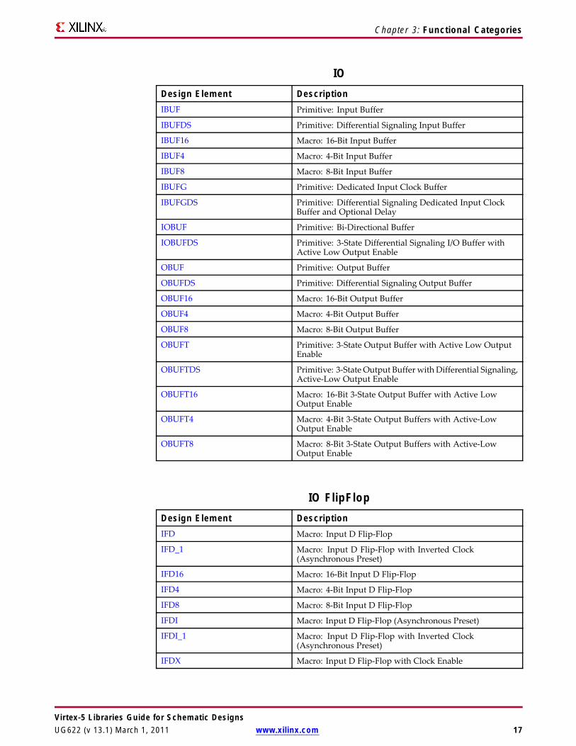
IODesign Element DescriptionIBUF Primitive: Input Buffer
IBUFDS Primitive: Differential Signaling Input Buffer
IBUF16 Macro: 16-Bit Input Buffer
IBUF4 Macro: 4-Bit Input Buffer
IBUF8 Macro: 8-Bit Input Buffer
IBUFG Primitive: Dedicated Input Clock Buffer
IBUFGDS Primitive: Differential Signaling Dedicated Input ClockBuffer and Optional Delay
IOBUF Primitive: Bi-Directional Buffer
IOBUFDS Primitive: 3-State Differential Signaling I/O Buffer withActive Low Output Enable
OBUF Primitive: Output Buffer
OBUFDS Primitive: Differential Signaling Output Buffer
OBUF16 Macro: 16-Bit Output Buffer
OBUF4 Macro: 4-Bit Output Buffer
OBUF8 Macro: 8-Bit Output Buffer
OBUFT Primitive: 3-State Output Buffer with Active Low OutputEnable
OBUFTDS Primitive: 3-State Output Buffer with Differential Signaling,Active-Low Output Enable
OBUFT16 Macro: 16-Bit 3-State Output Buffer with Active LowOutput Enable
OBUFT4 Macro: 4-Bit 3-State Output Buffers with Active-LowOutput Enable
OBUFT8 Macro: 8-Bit 3-State Output Buffers with Active-LowOutput Enable
IO FlipFlopDesign Element DescriptionIFD Macro: Input D Flip-Flop
IFD_1 Macro: Input D Flip-Flop with Inverted Clock(Asynchronous Preset)
IFD16 Macro: 16-Bit Input D Flip-Flop
IFD4 Macro: 4-Bit Input D Flip-Flop
IFD8 Macro: 8-Bit Input D Flip-Flop
IFDI Macro: Input D Flip-Flop (Asynchronous Preset)
IFDI_1 Macro: Input D Flip-Flop with Inverted Clock(Asynchronous Preset)
IFDX Macro: Input D Flip-Flop with Clock Enable
Virtex-5 Libraries Guide for Schematic DesignsUG622 (v 13.1) March 1, 2011 www.xilinx.com 17

Chapter 3: Functional Categories
Design Element DescriptionIFDX_1 Macro: Input D Flip-Flop with Inverted Clock and Clock
Enable
IFDX16 Macro: 16-Bit Input D Flip-Flops with Clock Enable
IFDX4 Macro: 4-Bit Input D Flip-Flop with Clock Enable
IFDX8 Macro: 8-Bit Input D Flip-Flop with Clock Enable
OFD Macro: Output D Flip-Flop
OFD_1 Macro: Output D Flip-Flop with Inverted Clock
OFD16 Macro: 16-Bit Output D Flip-Flop
OFD4 Macro: 4-Bit Output D Flip-Flop
OFD8 Macro: 8-Bit Output D Flip-Flop
OFDE Macro: D Flip-Flop with Active-High Enable OutputBuffers
OFDE_1 Macro: D Flip-Flop with Active-High Enable Output Bufferand Inverted Clock
OFDE4 Macro: 4-Bit D Flip-Flop with Active-High Enable OutputBuffers
OFDE8 Macro: 8-Bit D Flip-Flop with Active-High Enable OutputBuffers
OFDE16 Macro: 16-Bit D Flip-Flop with Active-High Enable OutputBuffers
OFDI Macro: Output D Flip-Flop (Asynchronous Preset)
OFDI_1 Macro: Output D Flip-Flop with Inverted Clock(Asynchronous Preset)
OFDT Macro: D Flip-Flop with Active-Low 3-State Output Buffer
OFDT_1 Macro: D Flip-Flop with Active-Low 3-State Output Bufferand Inverted Clock
OFDT16 Macro: 16-Bit D Flip-Flop with Active-Low 3-State OutputBuffers
OFDT4 Macro: 4-Bit D Flip-Flop with Active-Low 3-State OutputBuffers
OFDT8 Macro: 8-Bit D Flip-Flop with Active-Low 3-State OutputBuffers
OFDX Macro: Output D Flip-Flop with Clock Enable
OFDX_1 Macro: Output D Flip-Flop with Inverted Clock and ClockEnable
OFDX16 Macro: 16-Bit Output D Flip-Flop with Clock Enable
OFDX4 Macro: 4-Bit Output D Flip-Flop with Clock Enable
OFDX8 Macro: 8-Bit Output D Flip-Flop with Clock Enable
OFDXI Macro: Output D Flip-Flop with Clock Enable(Asynchronous Preset)
OFDXI_1 Macro: Output D Flip-Flop with Inverted Clock and ClockEnable (Asynchronous Preset)
Virtex-5 Libraries Guide for Schematic Designs18 www.xilinx.com UG622 (v 13.1) March 1, 2011
Chapter 3: Functional Categories
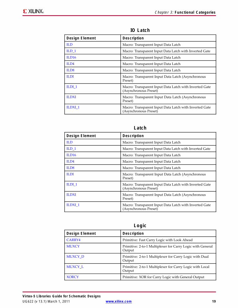
IO LatchDesign Element DescriptionILD Macro: Transparent Input Data Latch
ILD_1 Macro: Transparent Input Data Latch with Inverted Gate
ILD16 Macro: Transparent Input Data Latch
ILD4 Macro: Transparent Input Data Latch
ILD8 Macro: Transparent Input Data Latch
ILDI Macro: Transparent Input Data Latch (AsynchronousPreset)
ILDI_1 Macro: Transparent Input Data Latch with Inverted Gate(Asynchronous Preset)
ILDXI Macro: Transparent Input Data Latch (AsynchronousPreset)
ILDXI_1 Macro: Transparent Input Data Latch with Inverted Gate(Asynchronous Preset)
LatchDesign Element DescriptionILD Macro: Transparent Input Data Latch
ILD_1 Macro: Transparent Input Data Latch with Inverted Gate
ILD16 Macro: Transparent Input Data Latch
ILD4 Macro: Transparent Input Data Latch
ILD8 Macro: Transparent Input Data Latch
ILDI Macro: Transparent Input Data Latch (AsynchronousPreset)
ILDI_1 Macro: Transparent Input Data Latch with Inverted Gate(Asynchronous Preset)
ILDXI Macro: Transparent Input Data Latch (AsynchronousPreset)
ILDXI_1 Macro: Transparent Input Data Latch with Inverted Gate(Asynchronous Preset)
LogicDesign Element DescriptionCARRY4 Primitive: Fast Carry Logic with Look Ahead
MUXCY Primitive: 2-to-1 Multiplexer for Carry Logic with GeneralOutput
MUXCY_D Primitive: 2-to-1 Multiplexer for Carry Logic with DualOutput
MUXCY_L Primitive: 2-to-1 Multiplexer for Carry Logic with LocalOutput
XORCY Primitive: XOR for Carry Logic with General Output
Virtex-5 Libraries Guide for Schematic DesignsUG622 (v 13.1) March 1, 2011 www.xilinx.com 19
Chapter 3: Functional Categories
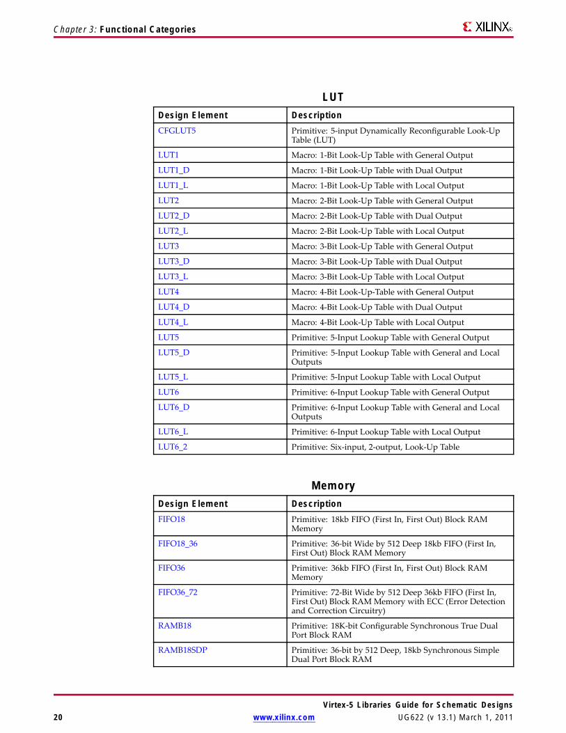
LUTDesign Element DescriptionCFGLUT5 Primitive: 5-input Dynamically Reconfigurable Look-Up
Table (LUT)
LUT1 Macro: 1-Bit Look-Up Table with General Output
LUT1_D Macro: 1-Bit Look-Up Table with Dual Output
LUT1_L Macro: 1-Bit Look-Up Table with Local Output
LUT2 Macro: 2-Bit Look-Up Table with General Output
LUT2_D Macro: 2-Bit Look-Up Table with Dual Output
LUT2_L Macro: 2-Bit Look-Up Table with Local Output
LUT3 Macro: 3-Bit Look-Up Table with General Output
LUT3_D Macro: 3-Bit Look-Up Table with Dual Output
LUT3_L Macro: 3-Bit Look-Up Table with Local Output
LUT4 Macro: 4-Bit Look-Up-Table with General Output
LUT4_D Macro: 4-Bit Look-Up Table with Dual Output
LUT4_L Macro: 4-Bit Look-Up Table with Local Output
LUT5 Primitive: 5-Input Lookup Table with General Output
LUT5_D Primitive: 5-Input Lookup Table with General and LocalOutputs
LUT5_L Primitive: 5-Input Lookup Table with Local Output
LUT6 Primitive: 6-Input Lookup Table with General Output
LUT6_D Primitive: 6-Input Lookup Table with General and LocalOutputs
LUT6_L Primitive: 6-Input Lookup Table with Local Output
LUT6_2 Primitive: Six-input, 2-output, Look-Up Table
MemoryDesign Element DescriptionFIFO18 Primitive: 18kb FIFO (First In, First Out) Block RAM
Memory
FIFO18_36 Primitive: 36-bit Wide by 512 Deep 18kb FIFO (First In,First Out) Block RAM Memory
FIFO36 Primitive: 36kb FIFO (First In, First Out) Block RAMMemory
FIFO36_72 Primitive: 72-Bit Wide by 512 Deep 36kb FIFO (First In,First Out) Block RAMMemory with ECC (Error Detectionand Correction Circuitry)
RAMB18 Primitive: 18K-bit Configurable Synchronous True DualPort Block RAM
RAMB18SDP Primitive: 36-bit by 512 Deep, 18kb Synchronous SimpleDual Port Block RAM
Virtex-5 Libraries Guide for Schematic Designs20 www.xilinx.com UG622 (v 13.1) March 1, 2011

Chapter 3: Functional Categories
Design Element DescriptionRAMB36 Primitive: 36kb Configurable Synchronous True Dual Port
Block RAM
RAMB36SDP Primitive: 72-bit by 512 Deep, 36kb Synchronous SimpleDual Port Block RAM with ECC (Error CorrectionCircuitry)
RAM16X1D Primitive: 16-Deep by 1-Wide Static Dual Port SynchronousRAM
RAM16X1D_1 Primitive: 16-Deep by 1-Wide Static Dual Port SynchronousRAM with Negative-Edge Clock
RAM16X1S Primitive: 16-Deep by 1-Wide Static Synchronous RAM
RAM16X1S_1 Primitive: 16-Deep by 1-Wide Static Synchronous RAMwith Negative-Edge Clock
RAM16X2S Primitive: 16-Deep by 2-Wide Static Synchronous RAM
RAM16X4S Primitive: 16-Deep by 4-Wide Static Synchronous RAM
RAM16X8S Primitive: 16-Deep by 8-Wide Static Synchronous RAM
RAM32M Primitive: 32-Deep by 8-bit Wide Multi Port RandomAccess Memory (Select RAM)
RAM32X1D Primitive: 32-Deep by 1-Wide Static Dual Port SynchronousRAM
RAM32X1S Primitive: 32-Deep by 1-Wide Static Synchronous RAM
RAM32X1S_1 Primitive: 32-Deep by 1-Wide Static Synchronous RAMwith Negative-Edge Clock
RAM32X2S Primitive: 32-Deep by 2-Wide Static Synchronous RAM
RAM32X4S Primitive: 32-Deep by 4-Wide Static Synchronous RAM
RAM32X8S Primitive: 32-Deep by 8-Wide Static Synchronous RAM
RAM64M Primitive: 64-Deep by 4-bit Wide Multi Port RandomAccess Memory (Select RAM)
RAM64X1D Primitive: 64-Deep by 1-Wide Dual Port Static SynchronousRAM
RAM64X1S Primitive: 64-Deep by 1-Wide Static Synchronous RAM
RAM64X1S_1 Primitive: 64-Deep by 1-Wide Static Synchronous RAMwith Negative-Edge Clock
RAM64X2S Primitive: 64-Deep by 2-Wide Static Synchronous RAM
RAM128X1D Primitive: 128-Deep by 1-Wide Dual Port Random AccessMemory (Select RAM)
RAM256X1S Primitive: 256-Deep by 1-Wide Random Access Memory(Select RAM)
ROM32X1 Primitive: 32-Deep by 1-Wide ROM
ROM64X1 Primitive: 64-Deep by 1-Wide ROM
ROM128X1 Primitive: 128-Deep by 1-Wide ROM
ROM256X1 Primitive: 256-Deep by 1-Wide ROM
Virtex-5 Libraries Guide for Schematic DesignsUG622 (v 13.1) March 1, 2011 www.xilinx.com 21
Chapter 3: Functional Categories
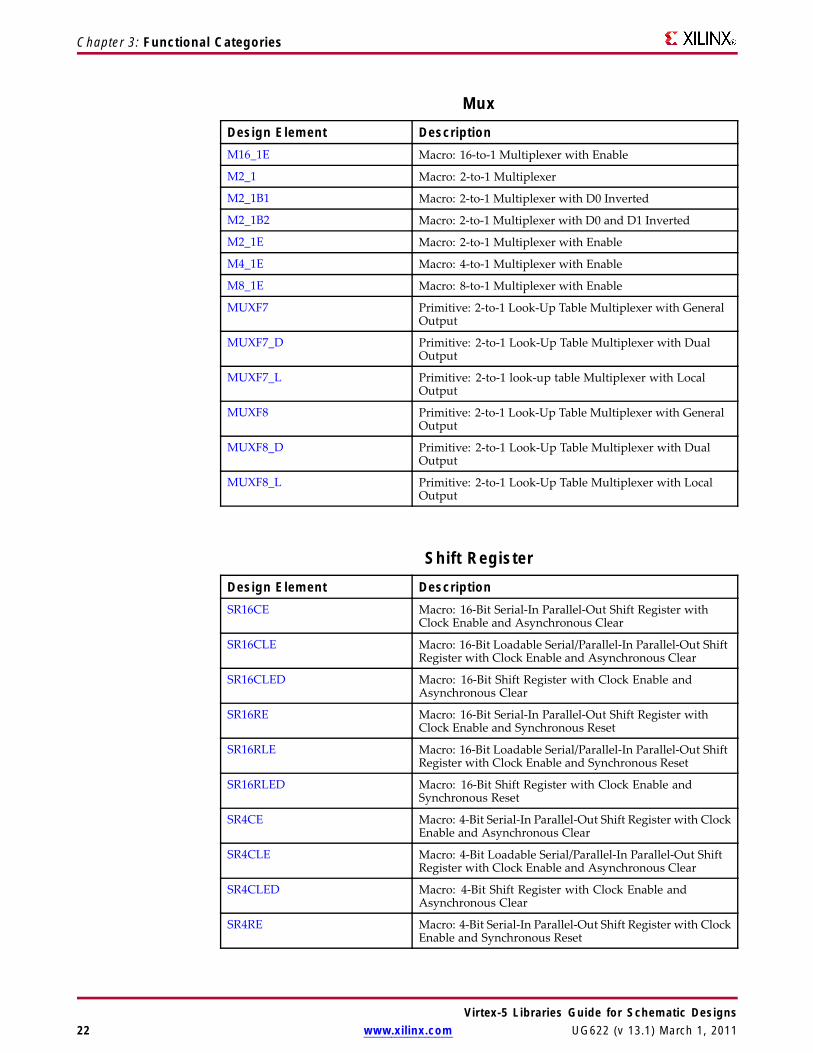
MuxDesign Element DescriptionM16_1E Macro: 16-to-1 Multiplexer with Enable
M2_1 Macro: 2-to-1 Multiplexer
M2_1B1 Macro: 2-to-1 Multiplexer with D0 Inverted
M2_1B2 Macro: 2-to-1 Multiplexer with D0 and D1 Inverted
M2_1E Macro: 2-to-1 Multiplexer with Enable
M4_1E Macro: 4-to-1 Multiplexer with Enable
M8_1E Macro: 8-to-1 Multiplexer with Enable
MUXF7 Primitive: 2-to-1 Look-Up Table Multiplexer with GeneralOutput
MUXF7_D Primitive: 2-to-1 Look-Up Table Multiplexer with DualOutput
MUXF7_L Primitive: 2-to-1 look-up table Multiplexer with LocalOutput
MUXF8 Primitive: 2-to-1 Look-Up Table Multiplexer with GeneralOutput
MUXF8_D Primitive: 2-to-1 Look-Up Table Multiplexer with DualOutput
MUXF8_L Primitive: 2-to-1 Look-Up Table Multiplexer with LocalOutput
Shift RegisterDesign Element DescriptionSR16CE Macro: 16-Bit Serial-In Parallel-Out Shift Register with
Clock Enable and Asynchronous Clear
SR16CLE Macro: 16-Bit Loadable Serial/Parallel-In Parallel-Out ShiftRegister with Clock Enable and Asynchronous Clear
SR16CLED Macro: 16-Bit Shift Register with Clock Enable andAsynchronous Clear
SR16RE Macro: 16-Bit Serial-In Parallel-Out Shift Register withClock Enable and Synchronous Reset
SR16RLE Macro: 16-Bit Loadable Serial/Parallel-In Parallel-Out ShiftRegister with Clock Enable and Synchronous Reset
SR16RLED Macro: 16-Bit Shift Register with Clock Enable andSynchronous Reset
SR4CE Macro: 4-Bit Serial-In Parallel-Out Shift Register with ClockEnable and Asynchronous Clear
SR4CLE Macro: 4-Bit Loadable Serial/Parallel-In Parallel-Out ShiftRegister with Clock Enable and Asynchronous Clear
SR4CLED Macro: 4-Bit Shift Register with Clock Enable andAsynchronous Clear
SR4RE Macro: 4-Bit Serial-In Parallel-Out Shift Register with ClockEnable and Synchronous Reset
Virtex-5 Libraries Guide for Schematic Designs22 www.xilinx.com UG622 (v 13.1) March 1, 2011
Chapter 3: Functional Categories
Design Element DescriptionSR4RLE Macro: 4-Bit Loadable Serial/Parallel-In Parallel-Out Shift
Register with Clock Enable and Synchronous Reset
SR4RLED Macro: 4-Bit Shift Register with Clock Enable andSynchronous Reset
SR8CE Macro: 8-Bit Serial-In Parallel-Out Shift Register with ClockEnable and Asynchronous Clear
SR8CLE Macro: 8-Bit Loadable Serial/Parallel-In Parallel-Out ShiftRegister with Clock Enable and Asynchronous Clear
SR8CLED Macro: 8-Bit Shift Register with Clock Enable andAsynchronous Clear
SR8RE Macro: 8-Bit Serial-In Parallel-Out Shift Register with ClockEnable and Synchronous Reset
SR8RLE Macro: 8-Bit Loadable Serial/Parallel-In Parallel-Out ShiftRegister with Clock Enable and Synchronous Reset
SR8RLED Macro: 8-Bit Shift Register with Clock Enable andSynchronous Reset
SRL16 Primitive: 16-Bit Shift Register Look-Up Table (LUT)
SRL16_1 Primitive: 16-Bit Shift Register Look-Up Table (LUT) withNegative-Edge Clock
SRL16E Primitive: 16-Bit Shift Register Look-Up Table (LUT) withClock Enable
SRL16E_1 Primitive: 16-Bit Shift Register Look-Up Table (LUT) withNegative-Edge Clock and Clock Enable
SRLC16 Primitive: 16-Bit Shift Register Look-Up Table (LUT) withCarry
SRLC16_1 Primitive: 16-Bit Shift Register Look-Up Table (LUT) withCarry and Negative-Edge Clock
SRLC16E Primitive: 16-Bit Shift Register Look-Up Table (LUT) withCarry and Clock Enable
SRLC16E_1 Primitive: 16-Bit Shift Register Look-Up Table (LUT) withCarry, Negative-Edge Clock, and Clock Enable
SRLC32E Primitive: 32 Clock Cycle, Variable Length Shift RegisterLook-Up Table (LUT) with Clock Enable
ShifterDesign Element DescriptionBRLSHFT4 Macro: 4-Bit Barrel Shifter
BRLSHFT8 Macro: 8-Bit Barrel Shifter
Virtex-5 Libraries Guide for Schematic DesignsUG622 (v 13.1) March 1, 2011 www.xilinx.com 23

Virtex-5 Libraries Guide for Schematic Designs24 www.xilinx.com UG622 (v 13.1) March 1, 2011

Chapter 4
About Design ElementsThis section describes the design elements that can be used with this architecture. Thedesign elements are organized alphabetically.
The following information is provided for each design element, where applicable:
• Name of element
• Brief description
• Schematic symbol (if any)
• Logic Table (if any)
• Port Descriptions (if any)
• Design Entry Method
• Available Attributes (if any)
• For more information
You can find examples of VHDL and Verilog instantiation code in the ISE software (inthe main menu, select Edit > Language Templates or in the Libraries Guide for HDLDesigns for this architecture.
Virtex-5 Libraries Guide for Schematic DesignsUG622 (v 13.1) March 1, 2011 www.xilinx.com 25
Chapter 4: About Design Elements
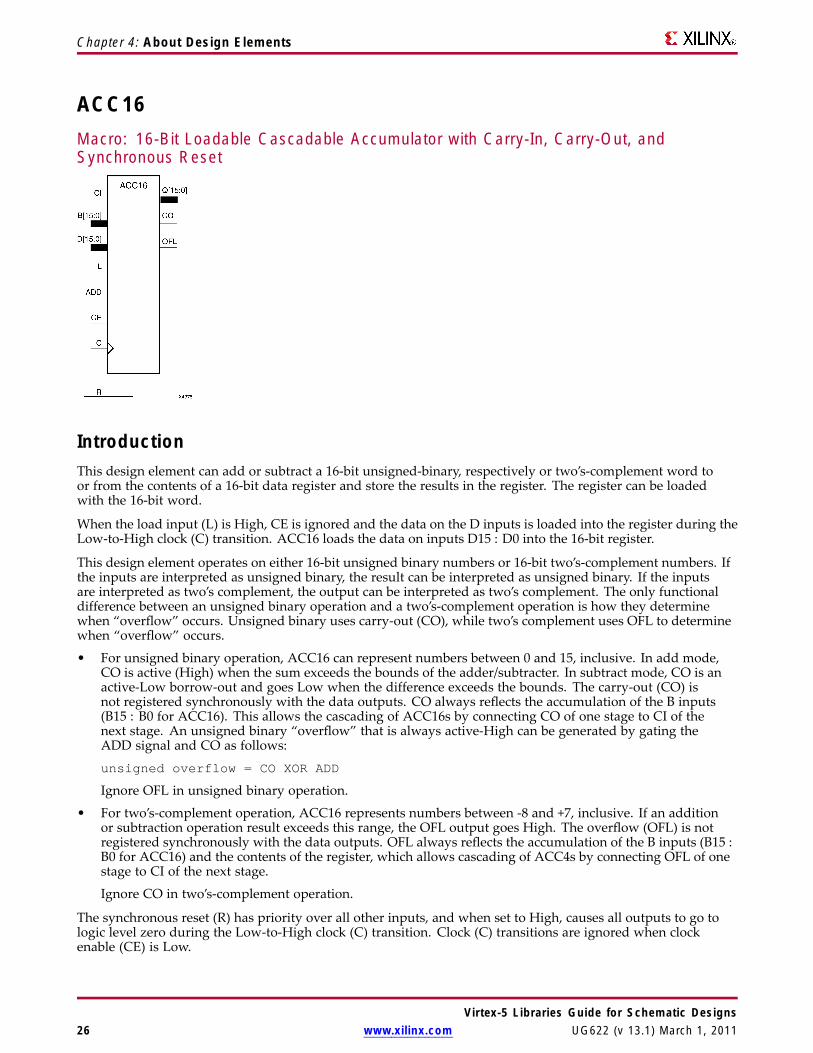
ACC16Macro: 16-Bit Loadable Cascadable Accumulator with Carry-In, Carry-Out, andSynchronous Reset
IntroductionThis design element can add or subtract a 16-bit unsigned-binary, respectively or two’s-complement word toor from the contents of a 16-bit data register and store the results in the register. The register can be loadedwith the 16-bit word.
When the load input (L) is High, CE is ignored and the data on the D inputs is loaded into the register during theLow-to-High clock (C) transition. ACC16 loads the data on inputs D15 : D0 into the 16-bit register.
This design element operates on either 16-bit unsigned binary numbers or 16-bit two’s-complement numbers. Ifthe inputs are interpreted as unsigned binary, the result can be interpreted as unsigned binary. If the inputsare interpreted as two’s complement, the output can be interpreted as two’s complement. The only functionaldifference between an unsigned binary operation and a two’s-complement operation is how they determinewhen “overflow” occurs. Unsigned binary uses carry-out (CO), while two’s complement uses OFL to determinewhen “overflow” occurs.
• For unsigned binary operation, ACC16 can represent numbers between 0 and 15, inclusive. In add mode,CO is active (High) when the sum exceeds the bounds of the adder/subtracter. In subtract mode, CO is anactive-Low borrow-out and goes Low when the difference exceeds the bounds. The carry-out (CO) isnot registered synchronously with the data outputs. CO always reflects the accumulation of the B inputs(B15 : B0 for ACC16). This allows the cascading of ACC16s by connecting CO of one stage to CI of thenext stage. An unsigned binary “overflow” that is always active-High can be generated by gating theADD signal and CO as follows:
unsigned overflow = CO XOR ADD
Ignore OFL in unsigned binary operation.
• For two’s-complement operation, ACC16 represents numbers between -8 and +7, inclusive. If an additionor subtraction operation result exceeds this range, the OFL output goes High. The overflow (OFL) is notregistered synchronously with the data outputs. OFL always reflects the accumulation of the B inputs (B15 :B0 for ACC16) and the contents of the register, which allows cascading of ACC4s by connecting OFL of onestage to CI of the next stage.
Ignore CO in two’s-complement operation.
The synchronous reset (R) has priority over all other inputs, and when set to High, causes all outputs to go tologic level zero during the Low-to-High clock (C) transition. Clock (C) transitions are ignored when clockenable (CE) is Low.
Virtex-5 Libraries Guide for Schematic Designs26 www.xilinx.com UG622 (v 13.1) March 1, 2011

Chapter 4: About Design Elements
This design element is asynchronously cleared, outputs Low, when power is applied. For FPGA devices,power-on conditions are simulated when global set/reset (GSR) is active. GSR defaults to active-High but can beinverted by adding an inverter in front of the GSR input of the appropriate STARTUP_architecture symbol.
Logic TableInput Output
R L CE ADD D C Q1 x x x x ↑ 0
0 1 x x Dn ↑ Dn
0 0 1 1 x ↑ Q0+Bn+CI
0 0 1 0 x ↑ Q0-Bn-CI
0 0 0 x x ↑ No Change
Q0: Previous value of Q
Bn: Value of Data input B
CI: Value of input CI
Design Entry MethodThis design element is only for use in schematics.
For More Information• See the Virtex-5 FPGA User Guide.
• See the Virtex-5 FPGA Data Sheet DC and Switching Characteristics.
Virtex-5 Libraries Guide for Schematic DesignsUG622 (v 13.1) March 1, 2011 www.xilinx.com 27

Chapter 4: About Design Elements
ACC4Macro: 4-Bit Loadable Cascadable Accumulator with Carry-In, Carry-Out, andSynchronous Reset
IntroductionThis design element can add or subtract a 4-bit unsigned-binary, respectively or two’s-complement word to orfrom the contents of a 4-bit data register and store the results in the register. The register can be loaded with the4-bit word.
When the load input (L) is High, CE is ignored and the data on the D inputs is loaded into the register during theLow-to-High clock (C) transition. ACC4 loads the data on inputs D3 : D0 into the 4-bit register.
This design element operates on either 4-bit unsigned binary numbers or 4-bit two’s-complement numbers. Ifthe inputs are interpreted as unsigned binary, the result can be interpreted as unsigned binary. If the inputsare interpreted as two’s complement, the output can be interpreted as two’s complement. The only functionaldifference between an unsigned binary operation and a two’s-complement operation is how they determinewhen “overflow” occurs. Unsigned binary uses carry-out (CO), while two’s complement uses OFL to determinewhen “overflow” occurs.• For unsigned binary operation, ACC4 can represent numbers between 0 and 15, inclusive. In add mode,
CO is active (High) when the sum exceeds the bounds of the adder/subtracter. In subtract mode, CO is anactive-Low borrow-out and goes Low when the difference exceeds the bounds. The carry-out (CO) isnot registered synchronously with the data outputs. CO always reflects the accumulation of the B inputs(B3 : B0 for ACC4). This allows the cascading of ACC4s by connecting CO of one stage to CI of the nextstage. An unsigned binary “overflow” that is always active-High can be generated by gating the ADDsignal and CO as follows:unsigned overflow = CO XOR ADD
Ignore OFL in unsigned binary operation.• For two’s-complement operation, ACC4 represents numbers between -8 and +7, inclusive. If an addition
or subtraction operation result exceeds this range, the OFL output goes High. The overflow (OFL) is notregistered synchronously with the data outputs. OFL always reflects the accumulation of the B inputs (B3 :B0 for ACC4) and the contents of the register, which allows cascading of ACC4s by connecting OFL of onestage to CI of the next stage.Ignore CO in two’s-complement operation.
Virtex-5 Libraries Guide for Schematic Designs28 www.xilinx.com UG622 (v 13.1) March 1, 2011

Chapter 4: About Design Elements
The synchronous reset (R) has priority over all other inputs, and when set to High, causes all outputs to go tologic level zero during the Low-to-High clock (C) transition. Clock (C) transitions are ignored when clockenable (CE) is Low.
This design element is asynchronously cleared, outputs Low, when power is applied. For FPGA devices,power-on conditions are simulated when global set/reset (GSR) is active. GSR defaults to active-High but can beinverted by adding an inverter in front of the GSR input of the appropriate STARTUP_architecture symbol.
Logic TableInput Output
R L CE ADD D C Q1 x x x x ↑ 0
0 1 x x Dn ↑ Dn
0 0 1 1 x ↑ Q0+Bn+CI
0 0 1 0 x ↑ Q0-Bn-CI
0 0 0 x x ↑ No Change
Q0: Previous value of Q
Bn: Value of Data input B
CI: Value of input CI
Design Entry MethodThis design element is only for use in schematics.
For More Information• See the Virtex-5 FPGA User Guide.
• See the Virtex-5 FPGA Data Sheet DC and Switching Characteristics.
Virtex-5 Libraries Guide for Schematic DesignsUG622 (v 13.1) March 1, 2011 www.xilinx.com 29

Chapter 4: About Design Elements
ACC8Macro: 8-Bit Loadable Cascadable Accumulator with Carry-In, Carry-Out, andSynchronous Reset
IntroductionThis design element can add or subtract a 8-bit unsigned-binary, respectively or two’s-complement word to orfrom the contents of a 8-bit data register and store the results in the register. The register can be loaded with the8-bit word.
When the load input (L) is High, CE is ignored and the data on the D inputs is loaded into the register during theLow-to-High clock (C) transition. ACC8 loads the data on inputs D7 : D0 into the 8-bit register.
This design element operates on either 8-bit unsigned binary numbers or 8-bit two’s-complement numbers. Ifthe inputs are interpreted as unsigned binary, the result can be interpreted as unsigned binary. If the inputsare interpreted as two’s complement, the output can be interpreted as two’s complement. The only functionaldifference between an unsigned binary operation and a two’s-complement operation is how they determinewhen “overflow” occurs. Unsigned binary uses carry-out (CO), while two’s complement uses OFL to determinewhen “overflow” occurs.
• For unsigned binary operation, ACC8 can represent numbers between 0 and 255, inclusive. In add mode,CO is active (High) when the sum exceeds the bounds of the adder/subtracter. In subtract mode, CO is anactive-Low borrow-out and goes Low when the difference exceeds the bounds. The carry-out (CO) isnot registered synchronously with the data outputs. CO always reflects the accumulation of the B inputs(B3 : B0 for ACC4). This allows the cascading of ACC8s by connecting CO of one stage to CI of the nextstage. An unsigned binary “overflow” that is always active-High can be generated by gating the ADDsignal and CO as follows:
unsigned overflow = CO XOR ADD
Ignore OFL in unsigned binary operation.
• For two’s-complement operation, ACC8 represents numbers between -128 and +127, inclusive. If an additionor subtraction operation result exceeds this range, the OFL output goes High. The overflow (OFL) is notregistered synchronously with the data outputs. OFL always reflects the accumulation of the B inputs (B3 :B0 for ACC8) and the contents of the register, which allows cascading of ACC8s by connecting OFL of onestage to CI of the next stage.
Ignore CO in two’s-complement operation.
The synchronous reset (R) has priority over all other inputs, and when set to High, causes all outputs to go tologic level zero during the Low-to-High clock (C) transition. Clock (C) transitions are ignored when clockenable (CE) is Low.
Virtex-5 Libraries Guide for Schematic Designs30 www.xilinx.com UG622 (v 13.1) March 1, 2011

Chapter 4: About Design Elements
This design element is asynchronously cleared, outputs Low, when power is applied. For FPGA devices,power-on conditions are simulated when global set/reset (GSR) is active. GSR defaults to active-High but can beinverted by adding an inverter in front of the GSR input of the appropriate STARTUP_architecture symbol.
Logic TableInput Output
R L CE ADD D C Q1 x x x x ↑ 0
0 1 x x Dn ↑ Dn
0 0 1 1 x ↑ Q0+Bn+CI
0 0 1 0 x ↑ Q0-Bn-CI
0 0 0 x x ↑ No Change
Q0: Previous value of Q
Bn: Value of Data input B
CI: Value of input CI
Design Entry MethodThis design element is only for use in schematics.
For More Information• See the Virtex-5 FPGA User Guide.
• See the Virtex-5 FPGA Data Sheet DC and Switching Characteristics.
Virtex-5 Libraries Guide for Schematic DesignsUG622 (v 13.1) March 1, 2011 www.xilinx.com 31
Chapter 4: About Design Elements
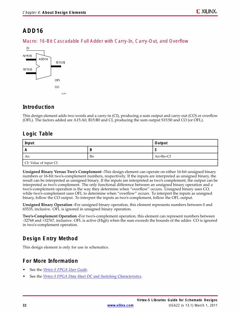
ADD16Macro: 16-Bit Cascadable Full Adder with Carry-In, Carry-Out, and Overflow
IntroductionThis design element adds two words and a carry-in (CI), producing a sum output and carry-out (CO) or overflow(OFL). The factors added are A15:A0, B15:B0 and CI, producing the sum output S15:S0 and CO (or OFL).
Logic TableInput Output
A B SAn Bn An+Bn+CI
CI: Value of input CI.
Unsigned Binary Versus Two’s Complement -This design element can operate on either 16-bit unsigned binarynumbers or 16-bit two’s-complement numbers, respectively. If the inputs are interpreted as unsigned binary, theresult can be interpreted as unsigned binary. If the inputs are interpreted as two’s complement, the output can beinterpreted as two’s complement. The only functional difference between an unsigned binary operation and atwo’s-complement operation is the way they determine when “overflow” occurs. Unsigned binary uses CO,while two’s-complement uses OFL to determine when “overflow” occurs. To interpret the inputs as unsignedbinary, follow the CO output. To interpret the inputs as two’s complement, follow the OFL output.
Unsigned Binary Operation -For unsigned binary operation, this element represents numbers between 0 and65535, inclusive. OFL is ignored in unsigned binary operation.
Two’s-Complement Operation -For two’s-complement operation, this element can represent numbers between-32768 and +32767, inclusive. OFL is active (High) when the sum exceeds the bounds of the adder. CO is ignoredin two’s-complement operation.
Design Entry MethodThis design element is only for use in schematics.
For More Information• See the Virtex-5 FPGA User Guide.
• See the Virtex-5 FPGA Data Sheet DC and Switching Characteristics.
Virtex-5 Libraries Guide for Schematic Designs32 www.xilinx.com UG622 (v 13.1) March 1, 2011
Chapter 4: About Design Elements
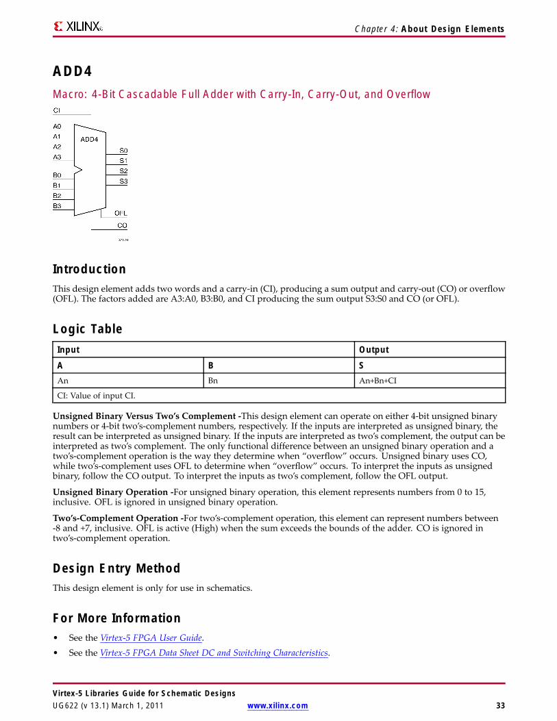
ADD4Macro: 4-Bit Cascadable Full Adder with Carry-In, Carry-Out, and Overflow
IntroductionThis design element adds two words and a carry-in (CI), producing a sum output and carry-out (CO) or overflow(OFL). The factors added are A3:A0, B3:B0, and CI producing the sum output S3:S0 and CO (or OFL).
Logic TableInput Output
A B SAn Bn An+Bn+CI
CI: Value of input CI.
Unsigned Binary Versus Two’s Complement -This design element can operate on either 4-bit unsigned binarynumbers or 4-bit two’s-complement numbers, respectively. If the inputs are interpreted as unsigned binary, theresult can be interpreted as unsigned binary. If the inputs are interpreted as two’s complement, the output can beinterpreted as two’s complement. The only functional difference between an unsigned binary operation and atwo’s-complement operation is the way they determine when “overflow” occurs. Unsigned binary uses CO,while two’s-complement uses OFL to determine when “overflow” occurs. To interpret the inputs as unsignedbinary, follow the CO output. To interpret the inputs as two’s complement, follow the OFL output.
Unsigned Binary Operation -For unsigned binary operation, this element represents numbers from 0 to 15,inclusive. OFL is ignored in unsigned binary operation.
Two’s-Complement Operation -For two’s-complement operation, this element can represent numbers between-8 and +7, inclusive. OFL is active (High) when the sum exceeds the bounds of the adder. CO is ignored intwo’s-complement operation.
Design Entry MethodThis design element is only for use in schematics.
For More Information• See the Virtex-5 FPGA User Guide.• See the Virtex-5 FPGA Data Sheet DC and Switching Characteristics.
Virtex-5 Libraries Guide for Schematic DesignsUG622 (v 13.1) March 1, 2011 www.xilinx.com 33
Chapter 4: About Design Elements
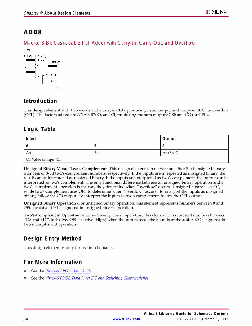
ADD8Macro: 8-Bit Cascadable Full Adder with Carry-In, Carry-Out, and Overflow
IntroductionThis design element adds two words and a carry-in (CI), producing a sum output and carry-out (CO) or overflow(OFL). The factors added are A7:A0, B7:B0, and CI, producing the sum output S7:S0 and CO (or OFL).
Logic TableInput Output
A B SAn Bn An+Bn+CI
CI: Value of input CI.
Unsigned Binary Versus Two’s Complement -This design element can operate on either 8-bit unsigned binarynumbers or 8-bit two’s-complement numbers, respectively. If the inputs are interpreted as unsigned binary, theresult can be interpreted as unsigned binary. If the inputs are interpreted as two’s complement, the output can beinterpreted as two’s complement. The only functional difference between an unsigned binary operation and atwo’s-complement operation is the way they determine when “overflow” occurs. Unsigned binary uses CO,while two’s-complement uses OFL to determine when “overflow” occurs. To interpret the inputs as unsignedbinary, follow the CO output. To interpret the inputs as two’s complement, follow the OFL output.
Unsigned Binary Operation -For unsigned binary operation, this element represents numbers between 0 and255, inclusive. OFL is ignored in unsigned binary operation.
Two’s-Complement Operation -For two’s-complement operation, this element can represent numbers between-128 and +127, inclusive. OFL is active (High) when the sum exceeds the bounds of the adder. CO is ignored intwo’s-complement operation.
Design Entry MethodThis design element is only for use in schematics.
For More Information• See the Virtex-5 FPGA User Guide.
• See the Virtex-5 FPGA Data Sheet DC and Switching Characteristics.
Virtex-5 Libraries Guide for Schematic Designs34 www.xilinx.com UG622 (v 13.1) March 1, 2011

Chapter 4: About Design Elements
ADSU16Macro: 16-Bit Cascadable Adder/Subtracter with Carry-In, Carry-Out, and Overflow
IntroductionWhen the ADD input is High, this element adds two 16-bit words (A15:A0 and B15:B0) and a carry-in (CI),producing a 16-bit sum output (S15:S0) and carry-out (CO) or overflow (OFL).
When the ADD input is Low, this element subtracts B15:B0 from A15:A0, producing a difference output anda carry-out (CO) or an overflow (OFL).
In add mode, CO and CI are active-High. In subtract mode, CO and CI are active-Low. OFL is active-High inadd and subtract modes.
Logic TableInput Output
ADD A B S1 An Bn An+Bn+CI*
0 An Bn An-Bn-CI*
CI*: ADD = 0, CI, CO active LOW
CI*: ADD = 1, CI, CO active HIGH
Unsigned Binary Versus Two’s Complement -This design element can operate on either 16-bit unsigned binarynumbers or 16-bit two’s-complement numbers. If the inputs are interpreted as unsigned binary, the resultcan be interpreted as unsigned binary. If the inputs are interpreted as two’s complement, the output can beinterpreted as two’s complement. The only functional difference between an unsigned binary operation and atwo’s-complement operation is the way they determine when “overflow” occurs. Unsigned binary uses CO,while two’s complement uses OFL to determine when “overflow” occurs.
With adder/subtracters, either unsigned binary or two’s-complement operations cause an overflow. If theresult crosses the overflow boundary, an overflow is generated. Similarly, when the result crosses the carry-outboundary, a carry-out is generated.
Unsigned Binary Operation -For unsigned binary operation, this element can represent numbers between 0 and65535, inclusive. In add mode, CO is active (High) when the sum exceeds the bounds of the adder/subtracter. Insubtract mode, CO is an active-Low borrow-out and goes Low when the difference exceeds the bounds.
An unsigned binary “overflow” that is always active-High can be generated by gating the ADD signal and COas follows:
unsigned overflow = CO XOR ADD
OFL is ignored in unsigned binary operation.
Virtex-5 Libraries Guide for Schematic DesignsUG622 (v 13.1) March 1, 2011 www.xilinx.com 35
Chapter 4: About Design Elements
Two’s-Complement Operation -For two’s-complement operation, this element can represent numbers between-32768 and +32767, inclusive.
If an addition or subtraction operation result exceeds this range, the OFL output goes High. CO is ignored intwo’s-complement operation.
Design Entry MethodThis design element is only for use in schematics.
For More Information• See the Virtex-5 FPGA User Guide.
• See the Virtex-5 FPGA Data Sheet DC and Switching Characteristics.
Virtex-5 Libraries Guide for Schematic Designs36 www.xilinx.com UG622 (v 13.1) March 1, 2011

Chapter 4: About Design Elements
ADSU4Macro: 4-Bit Cascadable Adder/Subtracter with Carry-In, Carry-Out, and Overflow
IntroductionWhen the ADD input is High, this element adds two 4-bit words (A3:A0 and B3:B0) and a carry-in (CI),producing a 4-bit sum output (S3:S0) and a carry-out (CO) or an overflow (OFL).
When the ADD input is Low, this element subtracts B3:B0 from A3:A0, producing a 4-bit difference output(S3:S0) and a carry-out (CO) or an overflow (OFL).
In add mode, CO and CI are active-High. In subtract mode, CO and CI are active-Low. OFL is active-High inadd and subtract modes.
Logic TableInput Output
ADD A B S1 An Bn An+Bn+CI*
0 An Bn An-Bn-CI*
CI*: ADD = 0, CI, CO active LOW
CI*: ADD = 1, CI, CO active HIGH
Unsigned Binary Versus Two’s Complement -This design element can operate on either 4-bit unsigned binarynumbers or 4-bit two’s-complement numbers. If the inputs are interpreted as unsigned binary, the resultcan be interpreted as unsigned binary. If the inputs are interpreted as two’s complement, the output can beinterpreted as two’s complement. The only functional difference between an unsigned binary operation and atwo’s-complement operation is the way they determine when “overflow” occurs. Unsigned binary uses CO,while two’s complement uses OFL to determine when “overflow” occurs.
With adder/subtracters, either unsigned binary or two’s-complement operations cause an overflow. If theresult crosses the overflow boundary, an overflow is generated. Similarly, when the result crosses the carry-outboundary, a carry-out is generated.
Unsigned Binary Operation -For unsigned binary operation, ADSU4 can represent numbers between 0 and15, inclusive. In add mode, CO is active (High) when the sum exceeds the bounds of the adder/subtracter. Insubtract mode, CO is an active-Low borrow-out and goes Low when the difference exceeds the bounds.
An unsigned binary “overflow” that is always active-High can be generated by gating the ADD signal and COas follows:
Virtex-5 Libraries Guide for Schematic DesignsUG622 (v 13.1) March 1, 2011 www.xilinx.com 37
Chapter 4: About Design Elements
unsigned overflow = CO XOR ADD
OFL is ignored in unsigned binary operation.
Two’s-Complement Operation -For two’s-complement operation, this element can represent numbers between-8 and +7, inclusive.
If an addition or subtraction operation result exceeds this range, the OFL output goes High. CO is ignored intwo’s-complement operation.
Design Entry MethodThis design element is only for use in schematics.
For More Information• See the Virtex-5 FPGA User Guide.
• See the Virtex-5 FPGA Data Sheet DC and Switching Characteristics.
Virtex-5 Libraries Guide for Schematic Designs38 www.xilinx.com UG622 (v 13.1) March 1, 2011

Chapter 4: About Design Elements
ADSU8Macro: 8-Bit Cascadable Adder/Subtracter with Carry-In, Carry-Out, and Overflow
IntroductionWhen the ADD input is High, this element adds two 8-bit words (A7:A0 and B7:B0) and a carry-in (CI),producing, an 8-bit sum output (S7:S0) and carry-out (CO) or an overflow (OFL).
When the ADD input is Low, this element subtracts B7:B0 from A7:A0, producing an 8-bit difference output(S7:S0) and a carry-out (CO) or an overflow (OFL).
In add mode, CO and CI are active-High. In subtract mode, CO and CI are active-Low. OFL is active-High inadd and subtract modes.
Logic TableInput Output
ADD A B S1 An Bn An+Bn+CI*
0 An Bn An-Bn-CI*
CI*: ADD = 0, CI, CO active LOW
CI*: ADD = 1, CI, CO active HIGH
Unsigned Binary Versus Two’s Complement -This design element can operate on either 8-bit unsigned binarynumbers or 8-bit two’s-complement numbers. If the inputs are interpreted as unsigned binary, the resultcan be interpreted as unsigned binary. If the inputs are interpreted as two’s complement, the output can beinterpreted as two’s complement. The only functional difference between an unsigned binary operation and atwo’s-complement operation is the way they determine when “overflow” occurs. Unsigned binary uses CO,while two’s complement uses OFL to determine when “overflow” occurs.
With adder/subtracters, either unsigned binary or two’s-complement operations cause an overflow. If theresult crosses the overflow boundary, an overflow is generated. Similarly, when the result crosses the carry-outboundary, a carry-out is generated.
Unsigned Binary Operation -For unsigned binary operation, this element can represent numbers between 0 and255, inclusive. In add mode, CO is active (High) when the sum exceeds the bounds of the adder/subtracter. Insubtract mode, CO is an active-Low borrow-out and goes Low when the difference exceeds the bounds.
An unsigned binary “overflow” that is always active-High can be generated by gating the ADD signal and COas follows:
unsigned overflow = CO XOR ADD
OFL is ignored in unsigned binary operation.
Virtex-5 Libraries Guide for Schematic DesignsUG622 (v 13.1) March 1, 2011 www.xilinx.com 39
Chapter 4: About Design Elements
Two’s-Complement Operation -For two’s-complement operation, this element can represent numbers between-128 and +127, inclusive.
If an addition or subtraction operation result exceeds this range, the OFL output goes High. CO is ignored intwo’s-complement operation.
Design Entry MethodThis design element is only for use in schematics.
For More Information• See the Virtex-5 FPGA User Guide.
• See the Virtex-5 FPGA Data Sheet DC and Switching Characteristics.
Virtex-5 Libraries Guide for Schematic Designs40 www.xilinx.com UG622 (v 13.1) March 1, 2011

Chapter 4: About Design Elements
AND12Macro: 12- Input AND Gate with Non-Inverted Inputs
IntroductionAND functions of up to five inputs are available in any combination of inverting and non-inverting inputs. ANDfunctions of six to nine inputs, 12 inputs, and 16 inputs are available with noninverting inputs. To make someor all inputs inverting, use external inverters. Because each input uses a CLB resource, replace functions withunused inputs with functions having the appropriate number of inputs.
Design Entry MethodThis design element is only for use in schematics.
For More Information• See the Virtex-5 FPGA User Guide.
• See the Virtex-5 FPGA Data Sheet DC and Switching Characteristics.
Virtex-5 Libraries Guide for Schematic DesignsUG622 (v 13.1) March 1, 2011 www.xilinx.com 41

Chapter 4: About Design Elements
AND16Macro: 16- Input AND Gate with Non-Inverted Inputs
IntroductionAND functions of up to five inputs are available in any combination of inverting and non-inverting inputs. ANDfunctions of six to nine inputs, 12 inputs, and 16 inputs are available with noninverting inputs. To make someor all inputs inverting, use external inverters. Because each input uses a CLB resource, replace functions withunused inputs with functions having the appropriate number of inputs.
Design Entry MethodThis design element is only for use in schematics.
For More Information• See the Virtex-5 FPGA User Guide.
• See the Virtex-5 FPGA Data Sheet DC and Switching Characteristics.
Virtex-5 Libraries Guide for Schematic Designs42 www.xilinx.com UG622 (v 13.1) March 1, 2011

Chapter 4: About Design Elements
AND2Primitive: 2-Input AND Gate with Non-Inverted Inputs
IntroductionAND functions of up to five inputs are available in any combination of inverting and non-inverting inputs. ANDfunctions of six to nine inputs, 12 inputs, and 16 inputs are available with noninverting inputs. To make someor all inputs inverting, use external inverters. Because each input uses a CLB resource, replace functions withunused inputs with functions having the appropriate number of inputs.
Design Entry MethodThis design element is only for use in schematics.
For More Information• See the Virtex-5 FPGA User Guide.
• See the Virtex-5 FPGA Data Sheet DC and Switching Characteristics.
Virtex-5 Libraries Guide for Schematic DesignsUG622 (v 13.1) March 1, 2011 www.xilinx.com 43
Chapter 4: About Design Elements
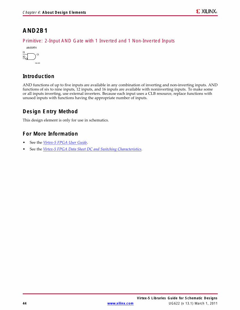
AND2B1Primitive: 2-Input AND Gate with 1 Inverted and 1 Non-Inverted Inputs
IntroductionAND functions of up to five inputs are available in any combination of inverting and non-inverting inputs. ANDfunctions of six to nine inputs, 12 inputs, and 16 inputs are available with noninverting inputs. To make someor all inputs inverting, use external inverters. Because each input uses a CLB resource, replace functions withunused inputs with functions having the appropriate number of inputs.
Design Entry MethodThis design element is only for use in schematics.
For More Information• See the Virtex-5 FPGA User Guide.
• See the Virtex-5 FPGA Data Sheet DC and Switching Characteristics.
Virtex-5 Libraries Guide for Schematic Designs44 www.xilinx.com UG622 (v 13.1) March 1, 2011
Chapter 4: About Design Elements
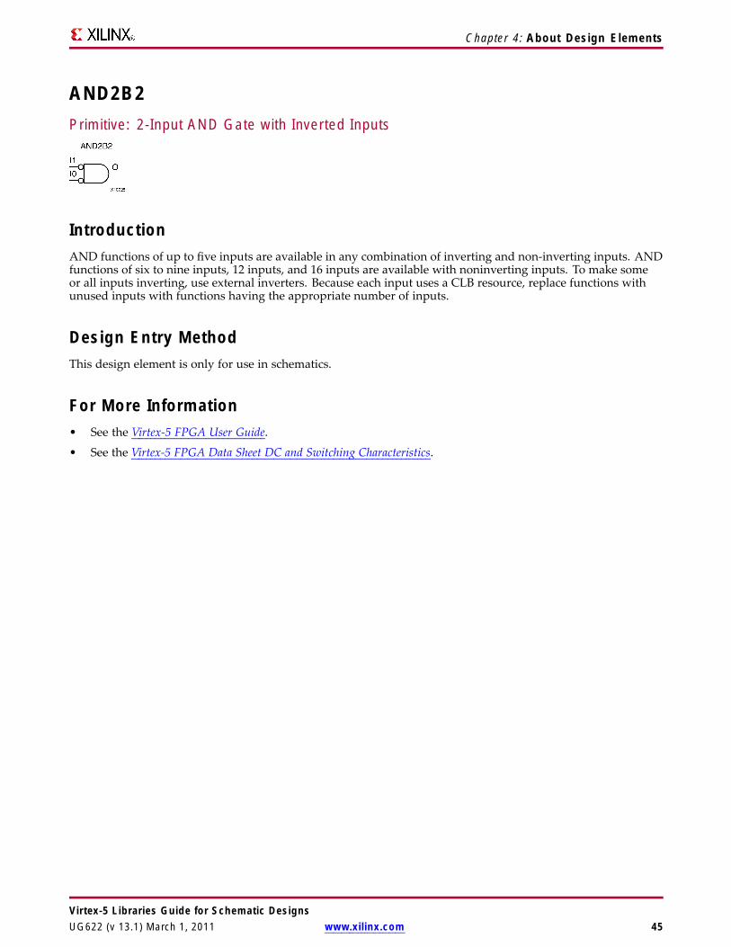
AND2B2Primitive: 2-Input AND Gate with Inverted Inputs
IntroductionAND functions of up to five inputs are available in any combination of inverting and non-inverting inputs. ANDfunctions of six to nine inputs, 12 inputs, and 16 inputs are available with noninverting inputs. To make someor all inputs inverting, use external inverters. Because each input uses a CLB resource, replace functions withunused inputs with functions having the appropriate number of inputs.
Design Entry MethodThis design element is only for use in schematics.
For More Information• See the Virtex-5 FPGA User Guide.
• See the Virtex-5 FPGA Data Sheet DC and Switching Characteristics.
Virtex-5 Libraries Guide for Schematic DesignsUG622 (v 13.1) March 1, 2011 www.xilinx.com 45

Chapter 4: About Design Elements
AND3Primitive: 3-Input AND Gate with Non-Inverted Inputs
IntroductionAND functions of up to five inputs are available in any combination of inverting and non-inverting inputs. ANDfunctions of six to nine inputs, 12 inputs, and 16 inputs are available with noninverting inputs. To make someor all inputs inverting, use external inverters. Because each input uses a CLB resource, replace functions withunused inputs with functions having the appropriate number of inputs.
Design Entry MethodThis design element is only for use in schematics.
For More Information• See the Virtex-5 FPGA User Guide.
• See the Virtex-5 FPGA Data Sheet DC and Switching Characteristics.
Virtex-5 Libraries Guide for Schematic Designs46 www.xilinx.com UG622 (v 13.1) March 1, 2011
Chapter 4: About Design Elements
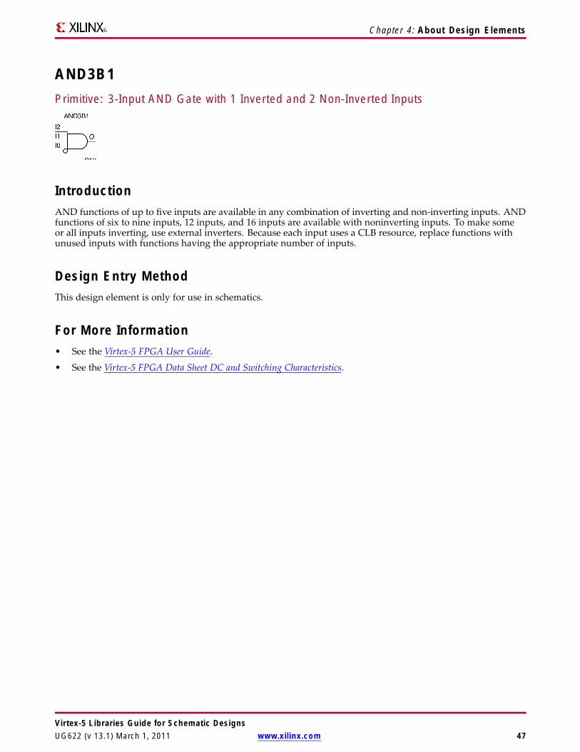
AND3B1Primitive: 3-Input AND Gate with 1 Inverted and 2 Non-Inverted Inputs
IntroductionAND functions of up to five inputs are available in any combination of inverting and non-inverting inputs. ANDfunctions of six to nine inputs, 12 inputs, and 16 inputs are available with noninverting inputs. To make someor all inputs inverting, use external inverters. Because each input uses a CLB resource, replace functions withunused inputs with functions having the appropriate number of inputs.
Design Entry MethodThis design element is only for use in schematics.
For More Information• See the Virtex-5 FPGA User Guide.
• See the Virtex-5 FPGA Data Sheet DC and Switching Characteristics.
Virtex-5 Libraries Guide for Schematic DesignsUG622 (v 13.1) March 1, 2011 www.xilinx.com 47
Chapter 4: About Design Elements
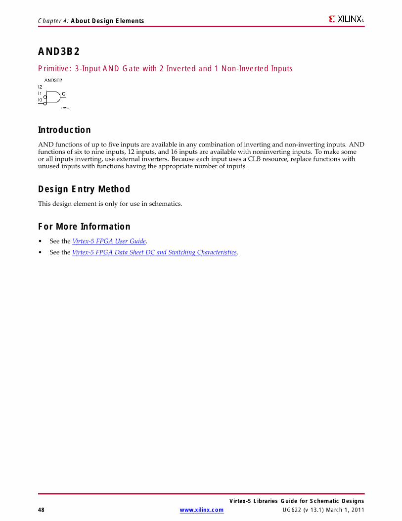
AND3B2Primitive: 3-Input AND Gate with 2 Inverted and 1 Non-Inverted Inputs
IntroductionAND functions of up to five inputs are available in any combination of inverting and non-inverting inputs. ANDfunctions of six to nine inputs, 12 inputs, and 16 inputs are available with noninverting inputs. To make someor all inputs inverting, use external inverters. Because each input uses a CLB resource, replace functions withunused inputs with functions having the appropriate number of inputs.
Design Entry MethodThis design element is only for use in schematics.
For More Information• See the Virtex-5 FPGA User Guide.
• See the Virtex-5 FPGA Data Sheet DC and Switching Characteristics.
Virtex-5 Libraries Guide for Schematic Designs48 www.xilinx.com UG622 (v 13.1) March 1, 2011
Chapter 4: About Design Elements
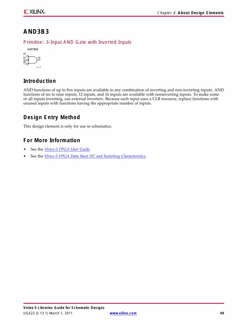
AND3B3Primitive: 3-Input AND Gate with Inverted Inputs
IntroductionAND functions of up to five inputs are available in any combination of inverting and non-inverting inputs. ANDfunctions of six to nine inputs, 12 inputs, and 16 inputs are available with noninverting inputs. To make someor all inputs inverting, use external inverters. Because each input uses a CLB resource, replace functions withunused inputs with functions having the appropriate number of inputs.
Design Entry MethodThis design element is only for use in schematics.
For More Information• See the Virtex-5 FPGA User Guide.
• See the Virtex-5 FPGA Data Sheet DC and Switching Characteristics.
Virtex-5 Libraries Guide for Schematic DesignsUG622 (v 13.1) March 1, 2011 www.xilinx.com 49

Chapter 4: About Design Elements
AND4Primitive: 4-Input AND Gate with Non-Inverted Inputs
IntroductionAND functions of up to five inputs are available in any combination of inverting and non-inverting inputs. ANDfunctions of six to nine inputs, 12 inputs, and 16 inputs are available with noninverting inputs. To make someor all inputs inverting, use external inverters. Because each input uses a CLB resource, replace functions withunused inputs with functions having the appropriate number of inputs.
Design Entry MethodThis design element is only for use in schematics.
For More Information• See the Virtex-5 FPGA User Guide.
• See the Virtex-5 FPGA Data Sheet DC and Switching Characteristics.
Virtex-5 Libraries Guide for Schematic Designs50 www.xilinx.com UG622 (v 13.1) March 1, 2011

Chapter 4: About Design Elements
AND4B1Primitive: 4-Input AND Gate with 1 Inverted and 3 Non-Inverted Inputs
IntroductionAND functions of up to five inputs are available in any combination of inverting and non-inverting inputs. ANDfunctions of six to nine inputs, 12 inputs, and 16 inputs are available with noninverting inputs. To make someor all inputs inverting, use external inverters. Because each input uses a CLB resource, replace functions withunused inputs with functions having the appropriate number of inputs.
Design Entry MethodThis design element is only for use in schematics.
For More Information• See the Virtex-5 FPGA User Guide.
• See the Virtex-5 FPGA Data Sheet DC and Switching Characteristics.
Virtex-5 Libraries Guide for Schematic DesignsUG622 (v 13.1) March 1, 2011 www.xilinx.com 51
Chapter 4: About Design Elements
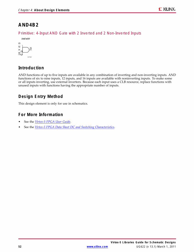
AND4B2Primitive: 4-Input AND Gate with 2 Inverted and 2 Non-Inverted Inputs
IntroductionAND functions of up to five inputs are available in any combination of inverting and non-inverting inputs. ANDfunctions of six to nine inputs, 12 inputs, and 16 inputs are available with noninverting inputs. To make someor all inputs inverting, use external inverters. Because each input uses a CLB resource, replace functions withunused inputs with functions having the appropriate number of inputs.
Design Entry MethodThis design element is only for use in schematics.
For More Information• See the Virtex-5 FPGA User Guide.
• See the Virtex-5 FPGA Data Sheet DC and Switching Characteristics.
Virtex-5 Libraries Guide for Schematic Designs52 www.xilinx.com UG622 (v 13.1) March 1, 2011
Chapter 4: About Design Elements
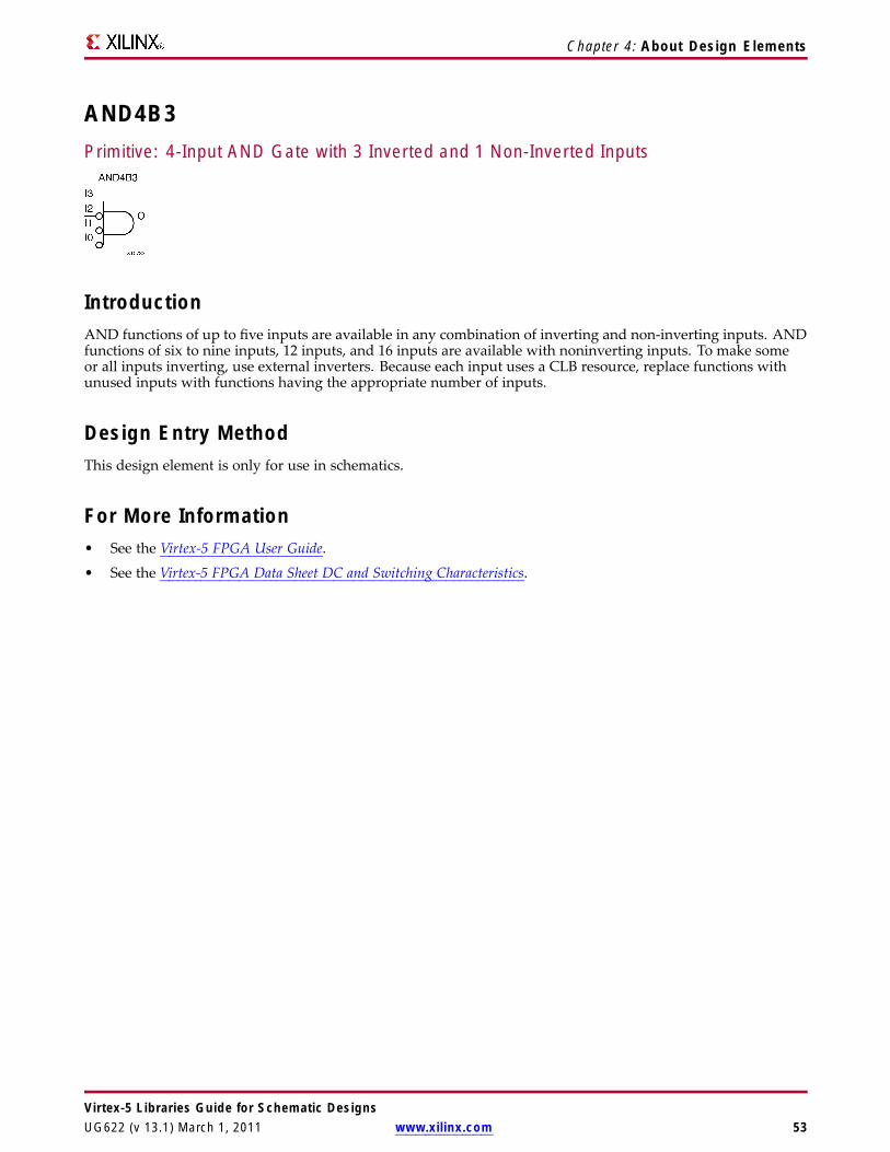
AND4B3Primitive: 4-Input AND Gate with 3 Inverted and 1 Non-Inverted Inputs
IntroductionAND functions of up to five inputs are available in any combination of inverting and non-inverting inputs. ANDfunctions of six to nine inputs, 12 inputs, and 16 inputs are available with noninverting inputs. To make someor all inputs inverting, use external inverters. Because each input uses a CLB resource, replace functions withunused inputs with functions having the appropriate number of inputs.
Design Entry MethodThis design element is only for use in schematics.
For More Information• See the Virtex-5 FPGA User Guide.
• See the Virtex-5 FPGA Data Sheet DC and Switching Characteristics.
Virtex-5 Libraries Guide for Schematic DesignsUG622 (v 13.1) March 1, 2011 www.xilinx.com 53
Chapter 4: About Design Elements
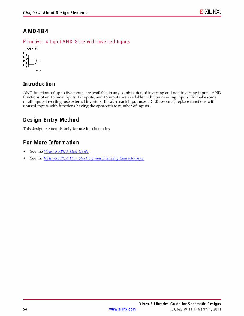
AND4B4Primitive: 4-Input AND Gate with Inverted Inputs
IntroductionAND functions of up to five inputs are available in any combination of inverting and non-inverting inputs. ANDfunctions of six to nine inputs, 12 inputs, and 16 inputs are available with noninverting inputs. To make someor all inputs inverting, use external inverters. Because each input uses a CLB resource, replace functions withunused inputs with functions having the appropriate number of inputs.
Design Entry MethodThis design element is only for use in schematics.
For More Information• See the Virtex-5 FPGA User Guide.
• See the Virtex-5 FPGA Data Sheet DC and Switching Characteristics.
Virtex-5 Libraries Guide for Schematic Designs54 www.xilinx.com UG622 (v 13.1) March 1, 2011

Chapter 4: About Design Elements
AND5Primitive: 5-Input AND Gate with Non-Inverted Inputs
IntroductionAND functions of up to five inputs are available in any combination of inverting and non-inverting inputs. ANDfunctions of six to nine inputs, 12 inputs, and 16 inputs are available with noninverting inputs. To make someor all inputs inverting, use external inverters. Because each input uses a CLB resource, replace functions withunused inputs with functions having the appropriate number of inputs.
Design Entry MethodThis design element is only for use in schematics.
For More Information• See the Virtex-5 FPGA User Guide.
• See the Virtex-5 FPGA Data Sheet DC and Switching Characteristics.
Virtex-5 Libraries Guide for Schematic DesignsUG622 (v 13.1) March 1, 2011 www.xilinx.com 55

Chapter 4: About Design Elements
AND5B1Primitive: 5-Input AND Gate with 1 Inverted and 4 Non-Inverted Inputs
IntroductionAND functions of up to five inputs are available in any combination of inverting and non-inverting inputs. ANDfunctions of six to nine inputs, 12 inputs, and 16 inputs are available with noninverting inputs. To make someor all inputs inverting, use external inverters. Because each input uses a CLB resource, replace functions withunused inputs with functions having the appropriate number of inputs.
Design Entry MethodThis design element is only for use in schematics.
For More Information• See the Virtex-5 FPGA User Guide.
• See the Virtex-5 FPGA Data Sheet DC and Switching Characteristics.
Virtex-5 Libraries Guide for Schematic Designs56 www.xilinx.com UG622 (v 13.1) March 1, 2011

Chapter 4: About Design Elements
AND5B2Primitive: 5-Input AND Gate with 2 Inverted and 3 Non-Inverted Inputs
IntroductionAND functions of up to five inputs are available in any combination of inverting and non-inverting inputs. ANDfunctions of six to nine inputs, 12 inputs, and 16 inputs are available with noninverting inputs. To make someor all inputs inverting, use external inverters. Because each input uses a CLB resource, replace functions withunused inputs with functions having the appropriate number of inputs.
Design Entry MethodThis design element is only for use in schematics.
For More Information• See the Virtex-5 FPGA User Guide.
• See the Virtex-5 FPGA Data Sheet DC and Switching Characteristics.
Virtex-5 Libraries Guide for Schematic DesignsUG622 (v 13.1) March 1, 2011 www.xilinx.com 57

Chapter 4: About Design Elements
AND5B3Primitive: 5-Input AND Gate with 3 Inverted and 2 Non-Inverted Inputs
IntroductionAND functions of up to five inputs are available in any combination of inverting and non-inverting inputs. ANDfunctions of six to nine inputs, 12 inputs, and 16 inputs are available with noninverting inputs. To make someor all inputs inverting, use external inverters. Because each input uses a CLB resource, replace functions withunused inputs with functions having the appropriate number of inputs.
Design Entry MethodThis design element is only for use in schematics.
For More Information• See the Virtex-5 FPGA User Guide.
• See the Virtex-5 FPGA Data Sheet DC and Switching Characteristics.
Virtex-5 Libraries Guide for Schematic Designs58 www.xilinx.com UG622 (v 13.1) March 1, 2011

Chapter 4: About Design Elements
AND5B4Primitive: 5-Input AND Gate with 4 Inverted and 1 Non-Inverted Inputs
IntroductionAND functions of up to five inputs are available in any combination of inverting and non-inverting inputs. ANDfunctions of six to nine inputs, 12 inputs, and 16 inputs are available with noninverting inputs. To make someor all inputs inverting, use external inverters. Because each input uses a CLB resource, replace functions withunused inputs with functions having the appropriate number of inputs.
Design Entry MethodThis design element is only for use in schematics.
For More Information• See the Virtex-5 FPGA User Guide.
• See the Virtex-5 FPGA Data Sheet DC and Switching Characteristics.
Virtex-5 Libraries Guide for Schematic DesignsUG622 (v 13.1) March 1, 2011 www.xilinx.com 59

Chapter 4: About Design Elements
AND5B5Primitive: 5-Input AND Gate with Inverted Inputs
IntroductionAND functions of up to five inputs are available in any combination of inverting and non-inverting inputs. ANDfunctions of six to nine inputs, 12 inputs, and 16 inputs are available with noninverting inputs. To make someor all inputs inverting, use external inverters. Because each input uses a CLB resource, replace functions withunused inputs with functions having the appropriate number of inputs.
Design Entry MethodThis design element is only for use in schematics.
For More Information• See the Virtex-5 FPGA User Guide.
• See the Virtex-5 FPGA Data Sheet DC and Switching Characteristics.
Virtex-5 Libraries Guide for Schematic Designs60 www.xilinx.com UG622 (v 13.1) March 1, 2011

Chapter 4: About Design Elements
AND6Macro: 6-Input AND Gate with Non-Inverted Inputs
IntroductionAND functions of up to five inputs are available in any combination of inverting and non-inverting inputs. ANDfunctions of six to nine inputs, 12 inputs, and 16 inputs are available with noninverting inputs. To make someor all inputs inverting, use external inverters. Because each input uses a CLB resource, replace functions withunused inputs with functions having the appropriate number of inputs.
Design Entry MethodThis design element is only for use in schematics.
For More Information• See the Virtex-5 FPGA User Guide.
• See the Virtex-5 FPGA Data Sheet DC and Switching Characteristics.
Virtex-5 Libraries Guide for Schematic DesignsUG622 (v 13.1) March 1, 2011 www.xilinx.com 61

Chapter 4: About Design Elements
AND7Macro: 7-Input AND Gate with Non-Inverted Inputs
IntroductionAND functions of up to five inputs are available in any combination of inverting and non-inverting inputs. ANDfunctions of six to nine inputs, 12 inputs, and 16 inputs are available with noninverting inputs. To make someor all inputs inverting, use external inverters. Because each input uses a CLB resource, replace functions withunused inputs with functions having the appropriate number of inputs.
Design Entry MethodThis design element is only for use in schematics.
For More Information• See the Virtex-5 FPGA User Guide.
• See the Virtex-5 FPGA Data Sheet DC and Switching Characteristics.
Virtex-5 Libraries Guide for Schematic Designs62 www.xilinx.com UG622 (v 13.1) March 1, 2011
Chapter 4: About Design Elements
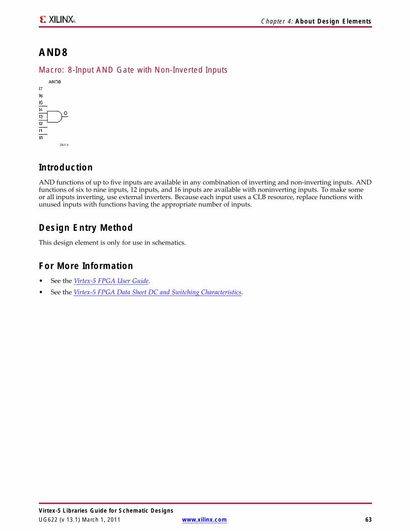
AND8Macro: 8-Input AND Gate with Non-Inverted Inputs
IntroductionAND functions of up to five inputs are available in any combination of inverting and non-inverting inputs. ANDfunctions of six to nine inputs, 12 inputs, and 16 inputs are available with noninverting inputs. To make someor all inputs inverting, use external inverters. Because each input uses a CLB resource, replace functions withunused inputs with functions having the appropriate number of inputs.
Design Entry MethodThis design element is only for use in schematics.
For More Information• See the Virtex-5 FPGA User Guide.
• See the Virtex-5 FPGA Data Sheet DC and Switching Characteristics.
Virtex-5 Libraries Guide for Schematic DesignsUG622 (v 13.1) March 1, 2011 www.xilinx.com 63

Chapter 4: About Design Elements
AND9Macro: 9-Input AND Gate with Non-Inverted Inputs
IntroductionAND functions of up to five inputs are available in any combination of inverting and non-inverting inputs. ANDfunctions of six to nine inputs, 12 inputs, and 16 inputs are available with noninverting inputs. To make someor all inputs inverting, use external inverters. Because each input uses a CLB resource, replace functions withunused inputs with functions having the appropriate number of inputs.
Design Entry MethodThis design element is only for use in schematics.
For More Information• See the Virtex-5 FPGA User Guide.
• See the Virtex-5 FPGA Data Sheet DC and Switching Characteristics.
Virtex-5 Libraries Guide for Schematic Designs64 www.xilinx.com UG622 (v 13.1) March 1, 2011

Chapter 4: About Design Elements
BRLSHFT4Macro: 4-Bit Barrel Shifter
IntroductionThis design element is a 4-bit barrel shifter that can rotate four inputs (I3 : I0) up to four places. The controlinputs (S1 and S0) determine the number of positions, from one to four, that the data is rotated. The four outputs(O3 : O0) reflect the shifted data inputs.
Logic TableInputs Outputs
S1 S0 I0 I1 I2 I3 O0 O1 O2 O30 0 a b c d a b c d
0 1 a b c d b c d a
1 0 a b c d c d a b
1 1 a b c d d a b c
Design Entry MethodThis design element is only for use in schematics.
For More Information• See the Virtex-5 FPGA User Guide.
• See the Virtex-5 FPGA Data Sheet DC and Switching Characteristics.
Virtex-5 Libraries Guide for Schematic DesignsUG622 (v 13.1) March 1, 2011 www.xilinx.com 65

Chapter 4: About Design Elements
BRLSHFT8Macro: 8-Bit Barrel Shifter
IntroductionThis design element is an 8-bit barrel shifter, can rotate the eight inputs (I7 : I0) up to eight places. The controlinputs (S2 : S0) determine the number of positions, from one to eight, that the data is rotated. The eight outputs(O7 : O0) reflect the shifted data inputs.
Logic TableInputs Outputs
S2 S1 S0 I0 I1 I2 I3 I4 I5 I6 I7 O0 O1 O2 O3 O4 O5 O6 O70 0 0 a b c d e f g h a b c d e f g h
0 0 1 a b c d e f g h b c d e f g h a
0 1 0 a b c d e f g h c d e f g h a b
0 1 1 a b c d e f g h d e f g h a b c
1 0 0 a b c d e f g h e f g h a b c d
1 0 1 a b c d e f g h f g h a b c d e
1 1 0 a b c d e f g h g h a b c d e f
1 1 1 a b c d e f g h h a b c d e f g
Design Entry MethodThis design element is only for use in schematics.
For More Information• See the Virtex-5 FPGA User Guide.• See the Virtex-5 FPGA Data Sheet DC and Switching Characteristics.
Virtex-5 Libraries Guide for Schematic Designs66 www.xilinx.com UG622 (v 13.1) March 1, 2011
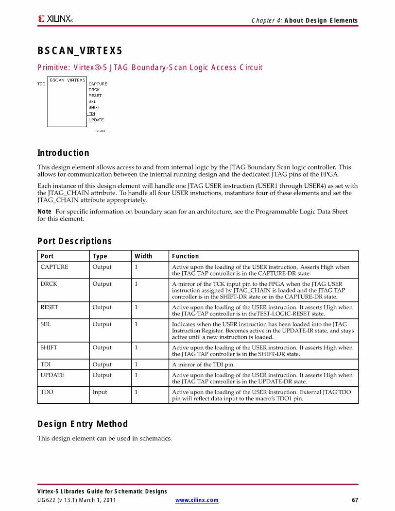
Chapter 4: About Design Elements
BSCAN_VIRTEX5Primitive: Virtex®-5 JTAG Boundary-Scan Logic Access Circuit
IntroductionThis design element allows access to and from internal logic by the JTAG Boundary Scan logic controller. Thisallows for communication between the internal running design and the dedicated JTAG pins of the FPGA.
Each instance of this design element will handle one JTAG USER instruction (USER1 through USER4) as set withthe JTAG_CHAIN attribute. To handle all four USER instuctions, instantiate four of these elements and set theJTAG_CHAIN attribute appropriately.
Note For specific information on boundary scan for an architecture, see the Programmable Logic Data Sheetfor this element.
Port DescriptionsPort Type Width FunctionCAPTURE Output 1 Active upon the loading of the USER instruction. Asserts High when
the JTAG TAP controller is in the CAPTURE-DR state.
DRCK Output 1 A mirror of the TCK input pin to the FPGA when the JTAG USERinstruction assigned by JTAG_CHAIN is loaded and the JTAG TAPcontroller is in the SHIFT-DR state or in the CAPTURE-DR state.
RESET Output 1 Active upon the loading of the USER instruction. It asserts High whenthe JTAG TAP controller is in theTEST-LOGIC-RESET state.
SEL Output 1 Indicates when the USER instruction has been loaded into the JTAGInstruction Register. Becomes active in the UPDATE-IR state, and staysactive until a new instruction is loaded.
SHIFT Output 1 Active upon the loading of the USER instruction. It asserts High whenthe JTAG TAP controller is in the SHIFT-DR state.
TDI Output 1 A mirror of the TDI pin.
UPDATE Output 1 Active upon the loading of the USER instruction. It asserts High whenthe JTAG TAP controller is in the UPDATE-DR state.
TDO Input 1 Active upon the loading of the USER instruction. External JTAG TDOpin will reflect data input to the macro’s TDO1 pin.
Design Entry MethodThis design element can be used in schematics.
Virtex-5 Libraries Guide for Schematic DesignsUG622 (v 13.1) March 1, 2011 www.xilinx.com 67
Chapter 4: About Design Elements
Available AttributesAttribute Type Allowed Values Default DescriptionJTAG_CHAIN Integer 1, 2, 3, 4 1 Sets the JTAGUSER instruction number that this instance
of the element will handle.
For More Information• See the Virtex-5 FPGA User Guide.
• See the Virtex-5 FPGA Data Sheet DC and Switching Characteristics.
Virtex-5 Libraries Guide for Schematic Designs68 www.xilinx.com UG622 (v 13.1) March 1, 2011

Chapter 4: About Design Elements
BUFPrimitive: General Purpose Buffer
IntroductionThis is a general-purpose, non-inverting buffer.
This element is not necessary and is removed by the partitioning software (MAP).
Design Entry MethodThis design element is only for use in schematics.
For More Information• See the Virtex-5 FPGA User Guide.
• See the Virtex-5 FPGA Data Sheet DC and Switching Characteristics.
Virtex-5 Libraries Guide for Schematic DesignsUG622 (v 13.1) March 1, 2011 www.xilinx.com 69

Chapter 4: About Design Elements
BUFCFPrimitive: Fast Connect Buffer
IntroductionThis design element is a single fast connect buffer used to connect the outputs of the LUTs and some dedicatedlogic directly to the input of another LUT. Using this buffer implies CLB packing. No more than four LUTsmay be connected together as a group.
Design Entry MethodThis design element can be used in schematics.
For More Information• See the Virtex-5 FPGA User Guide.
• See the Virtex-5 FPGA Data Sheet DC and Switching Characteristics.
Virtex-5 Libraries Guide for Schematic Designs70 www.xilinx.com UG622 (v 13.1) March 1, 2011
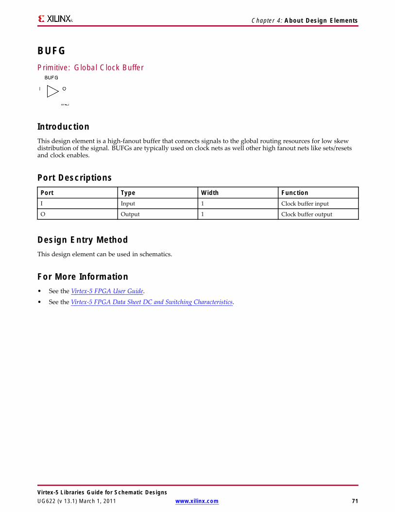
Chapter 4: About Design Elements
BUFGPrimitive: Global Clock Buffer
IntroductionThis design element is a high-fanout buffer that connects signals to the global routing resources for low skewdistribution of the signal. BUFGs are typically used on clock nets as well other high fanout nets like sets/resetsand clock enables.
Port DescriptionsPort Type Width FunctionI Input 1 Clock buffer input
O Output 1 Clock buffer output
Design Entry MethodThis design element can be used in schematics.
For More Information• See the Virtex-5 FPGA User Guide.
• See the Virtex-5 FPGA Data Sheet DC and Switching Characteristics.
Virtex-5 Libraries Guide for Schematic DesignsUG622 (v 13.1) March 1, 2011 www.xilinx.com 71

Chapter 4: About Design Elements
BUFGCEPrimitive: Global Clock Buffer with Clock Enable
IntroductionThis design element is a global clock buffer with a single gated input. Its O output is "0" when clock enable (CE)is Low (inactive). When clock enable (CE) is High, the I input is transferred to the O output.
Logic TableInputs Outputs
I CE OX 0 0
I 1 I
Port DescriptionsPort Type Width FunctionI Input 1 Clock buffer input
CE Input 1 Clock enable input
O Output 1 Clock buffer output
Design Entry MethodThis design element can be used in schematics.
For More Information• See the Virtex-5 FPGA User Guide.
• See the Virtex-5 FPGA Data Sheet DC and Switching Characteristics.
Virtex-5 Libraries Guide for Schematic Designs72 www.xilinx.com UG622 (v 13.1) March 1, 2011

Chapter 4: About Design Elements
BUFGCE_1Primitive: Global Clock Buffer with Clock Enable and Output State 1
IntroductionThis design element is a multiplexed global clock buffer with a single gated input. Its O output is High (1) whenclock enable (CE) is Low (inactive). When clock enable (CE) is High, the I input is transferred to the O output.
Logic TableInputs Outputs
I CE OX 0 1
I 1 I
Port DescriptionsPort Type Width FunctionI Input 1 Clock buffer input
CE Input 1 Clock enable input
O Output 1 Clock buffer output
Design Entry MethodThis design element can be used in schematics.
For More Information• See the Virtex-5 FPGA User Guide.
• See the Virtex-5 FPGA Data Sheet DC and Switching Characteristics.
Virtex-5 Libraries Guide for Schematic DesignsUG622 (v 13.1) March 1, 2011 www.xilinx.com 73

Chapter 4: About Design Elements
BUFGCTRLPrimitive: Global Clock MUX Buffer
IntroductionBUFGCTRL primitive is global clock buffer that is designed as a synchronous/asynchronous "glitch free" 2:1multiplexer with two clock inputs. Unlike global clock buffers that are found in previous generation of FPGAs,these clock buffers are designed with more control pins to provide a wider range of functionality and morerobust input switching. BUFGCTRL is not limited to clocking applications.
Port DescriptionsPort Type Width FunctionO Output 1 Clock Output pin
I0, I1 Input 1 (each) Clock Input:
I0 - Clock Input Pin
I1 - Clock Input Pin
CE0, CE1 Input 1 (each) Clock Enable Input. The CE pins represent the clock enable pinfor each clock inputs and are used to select the clock inputs. Asetup/hold time must be specified when you are using the CE pinto select inputs. Failure to meet this requirement could result ina clock glitch.
S0, S1 Input 1 (each) Clock Select Input. The S pins represent the clock select pin foreach clock inputs. When using the S pin as input select, there is asetup/hold time requirement. Unlike CE pins, failure to meet thisrequirement won’t result in a clock glitch. However, it can cause theoutput clock to appear one clock cycle later.
IGNORE0, IGNORE1 Input 1 (each) Clock Ignore Input. IGNORE pins are used whenever a designerwants to bypass the switching algorithm executed by the BUFGCTRL.
Design Entry MethodThis design element can be used in schematics.
Virtex-5 Libraries Guide for Schematic Designs74 www.xilinx.com UG622 (v 13.1) March 1, 2011
Chapter 4: About Design Elements
Available Attributes
Attribute TypeAllowedValues Default Description
INIT_OUT Integer 0, 1 0 Initializes the BUFGCTRL output to the specifiedvalue after configuration.
PRESELECT_I0 Boolean FALSE, TRUE FALSE If TRUE, BUFGCTRL output uses I0 input afterconfiguration.
PRESELECT_I1 Boolean FALSE, TRUE FALSE If TRUE, BUFGCTRL output uses I1 input afterconfiguration.
Note Both PRESELECT attributes might not be TRUE at the same time.
For More Information• See the Virtex-5 FPGA User Guide.
• See the Virtex-5 FPGA Data Sheet DC and Switching Characteristics.
Virtex-5 Libraries Guide for Schematic DesignsUG622 (v 13.1) March 1, 2011 www.xilinx.com 75
Chapter 4: About Design Elements
BUFGMUX_CTRLPrimitive: 2-to-1 Global Clock MUX Buffer
IntroductionThis design element is a global clock buffer with two clock inputs, one clock output, and a select line used tocleanly select between one of two clocks driving the global clocking resource. This component is based onBUFGCTRL, with some pins connected to logic High or Low. This element uses the S pin as the select pin for the2-to-1 MUX. S can switch anytime without causing a glitch on the output clock of the buffer.
Port DescriptionsPort Direction Width FunctionO Output 1 Clock Output
I0 Input 1 One of two Clock Inputs
I1 Input 1 One of two Clock Inputs
S Input 1 Select for I0 (S=0) or I1 (S=1)Clock Output
Design Entry MethodThis design element can be used in schematics.
For More Information• See the Virtex-5 FPGA User Guide.
• See the Virtex-5 FPGA Data Sheet DC and Switching Characteristics.
Virtex-5 Libraries Guide for Schematic Designs76 www.xilinx.com UG622 (v 13.1) March 1, 2011

Chapter 4: About Design Elements
BUFGPPrimitive: Global Buffer for Driving Clocks
IntroductionThis design element is a primary global buffer that is used to distribute high fan-out clock or control signalsthroughout in FPGA devices. It is equivalent to an IBUFG driving a BUFG.
Design Entry MethodThis design element is only for use in schematics.
For More Information• See the Virtex-5 FPGA User Guide.
• See the Virtex-5 FPGA Data Sheet DC and Switching Characteristics.
Virtex-5 Libraries Guide for Schematic DesignsUG622 (v 13.1) March 1, 2011 www.xilinx.com 77
Chapter 4: About Design Elements
BUFIOPrimitive: Local Clock Buffer for I/O
IntroductionThis design element is a clock buffer. It is simply a clock-in, clock-out buffer. It drives a dedicated clock netwithin the I/O column, independent of the global clock resources. Thus, these elements are ideally suited forsource-synchronous data capture (forwarded/receiver clock distribution). They can only be driven by clockcapable I/Os located in the same clock region. They drive the two adjacent I/O clock nets (for a total of up to threeclock regions), as well as the regional clock buffers (BUFR). These elements cannot drive logic resources (CLB,block RAM, etc.) because the I/O clock network only reaches the I/O column.
Port DescriptionsPort Type Width FunctionO Output 1 Clock output
I Input 1 Clock input
Design Entry MethodThis design element can be used in schematics.
For More Information• See the Virtex-5 FPGA User Guide.
• See the Virtex-5 FPGA Data Sheet DC and Switching Characteristics.
Virtex-5 Libraries Guide for Schematic Designs78 www.xilinx.com UG622 (v 13.1) March 1, 2011

Chapter 4: About Design Elements
BUFRPrimitive: Regional Clock Buffer for I/O and Logic Resources
IntroductionThe BUFR is a clock buffer. BUFRs drive clock signals to a dedicated clock net within a clock region, independentfrom the global clock tree. Each BUFR can drive the two regional clock nets in the region in which it is located,and the two clock nets in the adjacent clock regions (up to three clock regions). Unlike BUFIOs, BUFRs can drivethe I/O logic and logic resources (CLB, block RAM, etc.) in the existing and adjacent clock regions. BUFRs can bedriven by either the output from BUFIOs or local interconnect. In addition, BUFRs are capable of generatingdivided clock outputs with respect to the clock input. The divide value is an integer between one and eight.BUFRs are ideal for source-synchronous applications requiring clock domain crossing or serial-to-parallelconversion. There are two BUFRs in a typical clock region (two regional clock networks). The center columndoes not have BUFRs.
Port DescriptionsPort Type Width FunctionCE Input 1 Clock enable port. When asserted Low, this port disables the output
clock at port O. When asserted High, this port resets the counter usedto produce the divided clock output.
CLR Input 1 Counter reset for divided clock output. When asserted High, thisport resets the counter used to produce the divided clock output.
I Input 1 Clock input port. This port is the clock source port for BUFR. It canbe driven by BUFIO output or local interconnect.
O Output 1 Clock output port. This port drives the clock tracks in the clockregion of the BUFR and the two adjacent clock regions. This portdrives FPGA fabric, and IOBs.
Design Entry MethodThis design element can be used in schematics.
Available AttributesAttribute Type Allowed_Values Default DescriptionBUFR_DIVIDE String “BYPASS”, “1”, “2”, ”3”,
“4”, “5”, “6”, “7”, “8”“BYPASS” Defines whether the output clock is a
divided version of input clock.
SIM_DEVICE String VIRTEX4, VIRTEX5,VIRTEX6
VIRTEX4 Determine the CE latency for BUFR.
For More Information• See the Virtex-5 FPGA User Guide.• See the Virtex-5 FPGA Data Sheet DC and Switching Characteristics.
Virtex-5 Libraries Guide for Schematic DesignsUG622 (v 13.1) March 1, 2011 www.xilinx.com 79
Chapter 4: About Design Elements
CAPTURE_VIRTEX5Primitive: Virtex®-5 Readback Register Capture Control
IntroductionThis element provides user control and synchronization over when and how the capture register (flip-flop andlatch) information task is requested. The readback function is provided through dedicated configuration portinstructions. However, without this element, the readback data is synchronized to the configuration clock.Only register (flip-flop and latch) states can be captured. Although LUT RAM, SRL, and block RAM statesare readback, they cannot be captured.
An asserted high CAP signal indicates that the registers in the device are to be captured at the next Low-to-Highclock transition. By default, data is captured after every trigger when transition on CLK while CAP is asserted.To limit the readback operation to a single data capture, add the ONESHOT=TRUE attribute to this element.
Port DescriptionsPort Direction Width FunctionCAP Input 1 Readback capture trigger
CLK Input 1 Readback capture clock
Design Entry MethodThis design element can be used in schematics.
Connect all inputs and outputs to the design in order to ensure proper operation.
Available Attributes
Attribute TypeAllowedValues Default Description
ONESHOT Boolean TRUE, FALSE TRUE Specifies the procedure for performing single readback perCAP trigger.
For More Information• See the Virtex-5 FPGA User Guide.
• See the Virtex-5 FPGA Data Sheet DC and Switching Characteristics.
Virtex-5 Libraries Guide for Schematic Designs80 www.xilinx.com UG622 (v 13.1) March 1, 2011
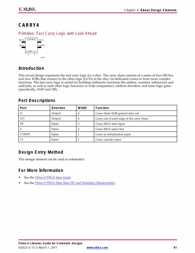
Chapter 4: About Design Elements
CARRY4Primitive: Fast Carry Logic with Look Ahead
IntroductionThis circuit design represents the fast carry logic for a slice. The carry chain consists of a series of four MUXesand four XORs that connect to the other logic (LUTs) in the slice via dedicated routes to form more complexfunctions. The fast carry logic is useful for building arithmetic functions like adders, counters, subtractors andadd/subs, as well as such other logic functions as wide comparators, address decoders, and some logic gates(specifically, AND and OR).
Port DescriptionsPort Direction Width FunctionO Output 4 Carry chain XOR general data out
CO Output 4 Carry-out of each stage of the carry chain
DI Input 4 Carry-MUX data input
S Input 4 Carry-MUX select line
CYINIT Input 1 Carry-in initialization input
CI Input 1 Carry cascade input
Design Entry MethodThis design element can be used in schematics.
For More Information• See the Virtex-5 FPGA User Guide.
• See the Virtex-5 FPGA Data Sheet DC and Switching Characteristics.
Virtex-5 Libraries Guide for Schematic DesignsUG622 (v 13.1) March 1, 2011 www.xilinx.com 81

Chapter 4: About Design Elements
CB16CEMacro: 16-Bit Cascadable Binary Counter with Clock Enable and Asynchronous Clear
IntroductionThis design element is an asynchronously clearable, cascadable binary counter. The asynchronous clear (CLR)input, when High, overrides all other inputs and forces the Q outputs, terminal count (TC), and clock enable out(CEO) to logic level zero, independent of clock transitions. The Q outputs increment when the clock enable input(CE) is High during the Low-to-High clock (C) transition. The counter ignores clock transitions when CE is Low.The TC output is High when all Q outputs are High.
Create larger counters by connecting the CEO output of each stage to the CE input of the next stage andconnecting the C and CLR inputs in parallel. CEO is active (High) when TC and CE are High. The maximumlength of the counter is determined by the accumulated CE-to-TC propagation delays versus the clock period.The clock period must be greater than n (tCE-TC), where n is the number of stages and the time tCE-TC is theCE-to-TC propagation delay of each stage. When cascading counters, use the CEO output if the counter uses theCE input or use the TC output if it does not.
This counter is asynchronously cleared, outputs Low, when power is applied. For FPGA devices, power-onconditions are simulated when global set/reset (GSR) is active. GSR defaults to active-High but can be invertedby adding an inverter in front of the GSR input of the appropriate STARTUP_architecture symbol.
Logic TableInputs Outputs
CLR CE C Qz-Q0 TC CEO1 X X 0 0 0
0 0 X No change No change 0
0 1 ↑ Inc TC CEO
z = bit width - 1
TC = Qz•Q(z-1)•Q(z-2)•...•Q0
CEO = TC•CE
Design Entry MethodThis design element is only for use in schematics.
For More Information• See the Virtex-5 FPGA User Guide.• See the Virtex-5 FPGA Data Sheet DC and Switching Characteristics.
Virtex-5 Libraries Guide for Schematic Designs82 www.xilinx.com UG622 (v 13.1) March 1, 2011

Virtex-5 Libraries Guide for Schematic Designs83 www.xilinx.com UG622 (v 13.1) March 1, 2011

Chapter 4: About Design Elements
CB16CLEMacro: 16-Bit Loadable Cascadable Binary Counters with Clock Enable and AsynchronousClear
IntroductionThis element is a synchronously loadable, asynchronously clearable, cascadable binary counter. Theasynchronous clear (CLR) input, when High, overrides all other inputs and forces the Q outputs, terminalcount (TC), and clock enable out (CEO) to logic level zero, independent of clock transitions. The data on theD inputs is loaded into the counter when the load enable input (L) is High during the Low-to-High clocktransition, independent of the state of clock enable (CE). The Q outputs increment when CE is High during theLow-to-High clock transition. The counter ignores clock transitions when CE is Low. The TC output is Highwhen all Q outputs are High.
Create larger counters by connecting the CEO output of each stage to the CE input of the next stage andconnecting the C, L, and CLR inputs in parallel. CEO is active (High) when TC and CE are High. The maximumlength of the counter is determined by the accumulated CE-to-TC propagation delays versus the clock period.The clock period must be greater than n (tCE-TC), where n is the number of stages and the time tCE-TC is theCE-to-TC propagation delay of each stage. When cascading counters, use the CEO output if the counter uses theCE input or use the TC output if it does not.
This counter is asynchronously cleared, outputs Low, when power is applied. For FPGA devices, power-onconditions are simulated when global set/reset (GSR) is active. GSR defaults to active-High but can be invertedby adding an inverter in front of the GSR input of the appropriate STARTUP_architecture symbol.
Virtex-5 Libraries Guide for Schematic Designs84 www.xilinx.com UG622 (v 13.1) March 1, 2011
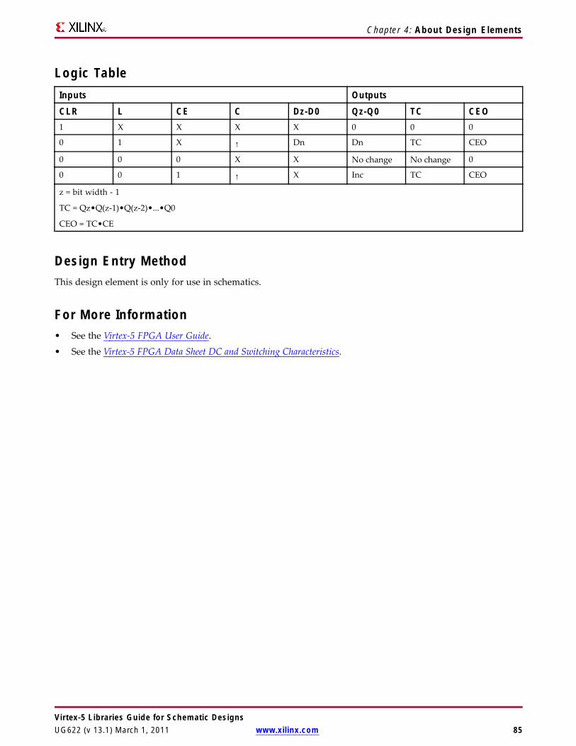
Chapter 4: About Design Elements
Logic TableInputs Outputs
CLR L CE C Dz-D0 Qz-Q0 TC CEO1 X X X X 0 0 0
0 1 X ↑ Dn Dn TC CEO
0 0 0 X X No change No change 0
0 0 1 ↑ X Inc TC CEO
z = bit width - 1
TC = Qz•Q(z-1)•Q(z-2)•...•Q0
CEO = TC•CE
Design Entry MethodThis design element is only for use in schematics.
For More Information• See the Virtex-5 FPGA User Guide.
• See the Virtex-5 FPGA Data Sheet DC and Switching Characteristics.
Virtex-5 Libraries Guide for Schematic DesignsUG622 (v 13.1) March 1, 2011 www.xilinx.com 85

Chapter 4: About Design Elements
CB16CLEDMacro: 16-Bit Loadable Cascadable Bidirectional Binary Counters with Clock Enableand Asynchronous Clear
IntroductionThis design element is a synchronously loadable, asynchronously clearable, cascadable, bidirectional binarycounter. The asynchronous clear (CLR) input, when High, overrides all other inputs and forces the Q outputs,terminal count (TC), and clock enable out (CEO) to logic level zero, independent of clock transitions. The data onthe D inputs is loaded into the counter when the load enable input (L) is High during the Low-to-High clock(C) transition, independent of the state of clock enable (CE). The Q outputs decrement when CE is High andUP is Low during the Low-to- High clock transition. The Q outputs increment when CE and UP are High. Thecounter ignores clock transitions when CE is Low.
For counting up, the TC output is High when all Q outputs and UP are High. For counting down, the TCoutput is High when all Q outputs and UP are Low.
Create larger counters by connecting the CEO output of each stage to the CE input of the next stage andconnecting the C, UP, L, and CLR inputs in parallel. CEO is active (High) when TC and CE are High. Themaximum length of the counter is determined by the accumulated CE-to-TC propagation delays versus the clockperiod. The clock period must be greater than n (tCE-TC), where n is the number of stages and the time tCE-TC isthe CE-to-TC propagation delay of each stage. When cascading counters, use the CEO output if the counteruses the CE input or use the TC output if it does not.
For CPLD parts, see “CB2X1”, “CB4X1”, “CB8X1”, “CB16X1” for high-performance cascadable, bidirectionalcounters.
This counter is asynchronously cleared, outputs Low, when power is applied. For FPGA devices, power-onconditions are simulated when global set/reset (GSR) is active. GSR defaults to active-High but can be invertedby adding an inverter in front of the GSR input of the appropriate STARTUP_architecture symbol.
Virtex-5 Libraries Guide for Schematic Designs86 www.xilinx.com UG622 (v 13.1) March 1, 2011
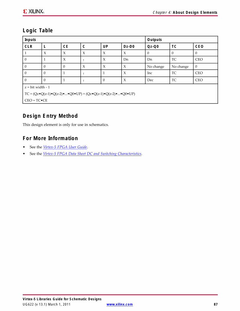
Chapter 4: About Design Elements
Logic TableInputs Outputs
CLR L CE C UP Dz-D0 Qz-Q0 TC CEO1 X X X X X 0 0 0
0 1 X ↑ X Dn Dn TC CEO
0 0 0 X X X No change No change 0
0 0 1 ↑ 1 X Inc TC CEO
0 0 1 ↑ 0 X Dec TC CEO
z = bit width - 1
TC = (Qz•Q(z-1)•Q(z-2)•...•Q0•UP) + (Qz•Q(z-1)•Q(z-2)•...•Q0•UP)
CEO = TC•CE
Design Entry MethodThis design element is only for use in schematics.
For More Information• See the Virtex-5 FPGA User Guide.
• See the Virtex-5 FPGA Data Sheet DC and Switching Characteristics.
Virtex-5 Libraries Guide for Schematic DesignsUG622 (v 13.1) March 1, 2011 www.xilinx.com 87
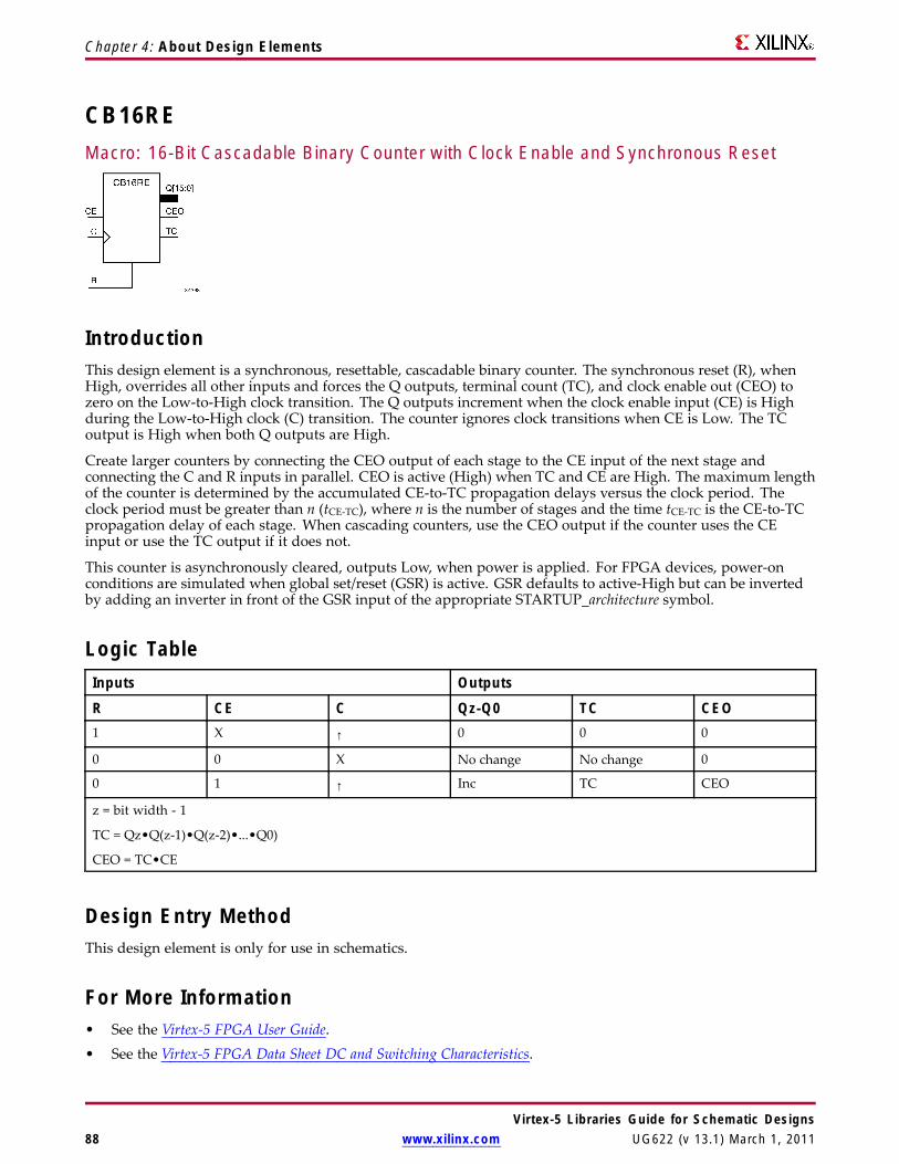
Chapter 4: About Design Elements
CB16REMacro: 16-Bit Cascadable Binary Counter with Clock Enable and Synchronous Reset
IntroductionThis design element is a synchronous, resettable, cascadable binary counter. The synchronous reset (R), whenHigh, overrides all other inputs and forces the Q outputs, terminal count (TC), and clock enable out (CEO) tozero on the Low-to-High clock transition. The Q outputs increment when the clock enable input (CE) is Highduring the Low-to-High clock (C) transition. The counter ignores clock transitions when CE is Low. The TCoutput is High when both Q outputs are High.
Create larger counters by connecting the CEO output of each stage to the CE input of the next stage andconnecting the C and R inputs in parallel. CEO is active (High) when TC and CE are High. The maximum lengthof the counter is determined by the accumulated CE-to-TC propagation delays versus the clock period. Theclock period must be greater than n (tCE-TC), where n is the number of stages and the time tCE-TC is the CE-to-TCpropagation delay of each stage. When cascading counters, use the CEO output if the counter uses the CEinput or use the TC output if it does not.
This counter is asynchronously cleared, outputs Low, when power is applied. For FPGA devices, power-onconditions are simulated when global set/reset (GSR) is active. GSR defaults to active-High but can be invertedby adding an inverter in front of the GSR input of the appropriate STARTUP_architecture symbol.
Logic TableInputs Outputs
R CE C Qz-Q0 TC CEO1 X ↑ 0 0 0
0 0 X No change No change 0
0 1 ↑ Inc TC CEO
z = bit width - 1
TC = Qz•Q(z-1)•Q(z-2)•...•Q0)
CEO = TC•CE
Design Entry MethodThis design element is only for use in schematics.
For More Information• See the Virtex-5 FPGA User Guide.• See the Virtex-5 FPGA Data Sheet DC and Switching Characteristics.
Virtex-5 Libraries Guide for Schematic Designs88 www.xilinx.com UG622 (v 13.1) March 1, 2011
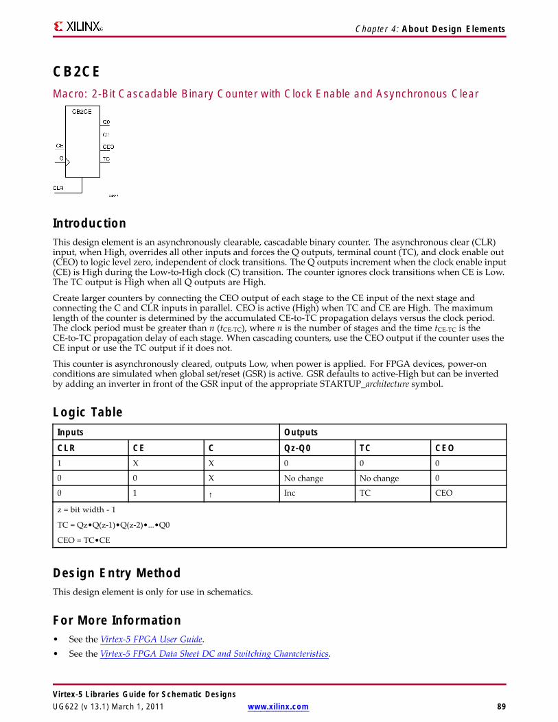
Chapter 4: About Design Elements
CB2CEMacro: 2-Bit Cascadable Binary Counter with Clock Enable and Asynchronous Clear
IntroductionThis design element is an asynchronously clearable, cascadable binary counter. The asynchronous clear (CLR)input, when High, overrides all other inputs and forces the Q outputs, terminal count (TC), and clock enable out(CEO) to logic level zero, independent of clock transitions. The Q outputs increment when the clock enable input(CE) is High during the Low-to-High clock (C) transition. The counter ignores clock transitions when CE is Low.The TC output is High when all Q outputs are High.
Create larger counters by connecting the CEO output of each stage to the CE input of the next stage andconnecting the C and CLR inputs in parallel. CEO is active (High) when TC and CE are High. The maximumlength of the counter is determined by the accumulated CE-to-TC propagation delays versus the clock period.The clock period must be greater than n (tCE-TC), where n is the number of stages and the time tCE-TC is theCE-to-TC propagation delay of each stage. When cascading counters, use the CEO output if the counter uses theCE input or use the TC output if it does not.
This counter is asynchronously cleared, outputs Low, when power is applied. For FPGA devices, power-onconditions are simulated when global set/reset (GSR) is active. GSR defaults to active-High but can be invertedby adding an inverter in front of the GSR input of the appropriate STARTUP_architecture symbol.
Logic TableInputs Outputs
CLR CE C Qz-Q0 TC CEO1 X X 0 0 0
0 0 X No change No change 0
0 1 ↑ Inc TC CEO
z = bit width - 1
TC = Qz•Q(z-1)•Q(z-2)•...•Q0
CEO = TC•CE
Design Entry MethodThis design element is only for use in schematics.
For More Information• See the Virtex-5 FPGA User Guide.• See the Virtex-5 FPGA Data Sheet DC and Switching Characteristics.
Virtex-5 Libraries Guide for Schematic DesignsUG622 (v 13.1) March 1, 2011 www.xilinx.com 89
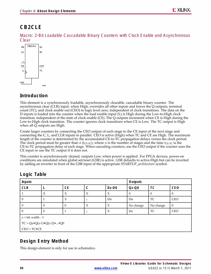
Chapter 4: About Design Elements
CB2CLEMacro: 2-Bit Loadable Cascadable Binary Counters with Clock Enable and AsynchronousClear
IntroductionThis element is a synchronously loadable, asynchronously clearable, cascadable binary counter. Theasynchronous clear (CLR) input, when High, overrides all other inputs and forces the Q outputs, terminalcount (TC), and clock enable out (CEO) to logic level zero, independent of clock transitions. The data on theD inputs is loaded into the counter when the load enable input (L) is High during the Low-to-High clocktransition, independent of the state of clock enable (CE). The Q outputs increment when CE is High during theLow-to-High clock transition. The counter ignores clock transitions when CE is Low. The TC output is Highwhen all Q outputs are High.
Create larger counters by connecting the CEO output of each stage to the CE input of the next stage andconnecting the C, L, and CLR inputs in parallel. CEO is active (High) when TC and CE are High. The maximumlength of the counter is determined by the accumulated CE-to-TC propagation delays versus the clock period.The clock period must be greater than n (tCE-TC), where n is the number of stages and the time tCE-TC is theCE-to-TC propagation delay of each stage. When cascading counters, use the CEO output if the counter uses theCE input or use the TC output if it does not.
This counter is asynchronously cleared, outputs Low, when power is applied. For FPGA devices, power-onconditions are simulated when global set/reset (GSR) is active. GSR defaults to active-High but can be invertedby adding an inverter in front of the GSR input of the appropriate STARTUP_architecture symbol.
Logic TableInputs Outputs
CLR L CE C Dz-D0 Qz-Q0 TC CEO1 X X X X 0 0 0
0 1 X ↑ Dn Dn TC CEO
0 0 0 X X No change No change 0
0 0 1 ↑ X Inc TC CEO
z = bit width - 1
TC = Qz•Q(z-1)•Q(z-2)•...•Q0
CEO = TC•CE
Design Entry MethodThis design element is only for use in schematics.
Virtex-5 Libraries Guide for Schematic Designs90 www.xilinx.com UG622 (v 13.1) March 1, 2011

Chapter 4: About Design Elements
For More Information• See the Virtex-5 FPGA User Guide.
• See the Virtex-5 FPGA Data Sheet DC and Switching Characteristics.
Virtex-5 Libraries Guide for Schematic DesignsUG622 (v 13.1) March 1, 2011 www.xilinx.com 91
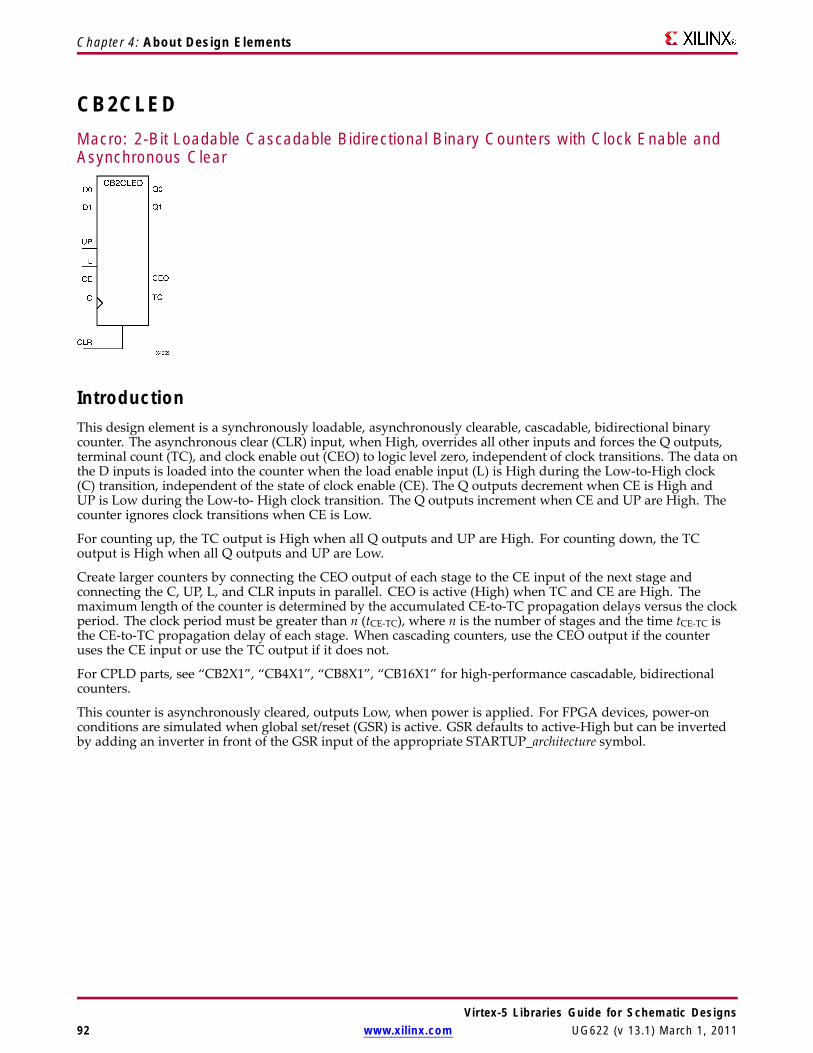
Chapter 4: About Design Elements
CB2CLEDMacro: 2-Bit Loadable Cascadable Bidirectional Binary Counters with Clock Enable andAsynchronous Clear
IntroductionThis design element is a synchronously loadable, asynchronously clearable, cascadable, bidirectional binarycounter. The asynchronous clear (CLR) input, when High, overrides all other inputs and forces the Q outputs,terminal count (TC), and clock enable out (CEO) to logic level zero, independent of clock transitions. The data onthe D inputs is loaded into the counter when the load enable input (L) is High during the Low-to-High clock(C) transition, independent of the state of clock enable (CE). The Q outputs decrement when CE is High andUP is Low during the Low-to- High clock transition. The Q outputs increment when CE and UP are High. Thecounter ignores clock transitions when CE is Low.
For counting up, the TC output is High when all Q outputs and UP are High. For counting down, the TCoutput is High when all Q outputs and UP are Low.
Create larger counters by connecting the CEO output of each stage to the CE input of the next stage andconnecting the C, UP, L, and CLR inputs in parallel. CEO is active (High) when TC and CE are High. Themaximum length of the counter is determined by the accumulated CE-to-TC propagation delays versus the clockperiod. The clock period must be greater than n (tCE-TC), where n is the number of stages and the time tCE-TC isthe CE-to-TC propagation delay of each stage. When cascading counters, use the CEO output if the counteruses the CE input or use the TC output if it does not.
For CPLD parts, see “CB2X1”, “CB4X1”, “CB8X1”, “CB16X1” for high-performance cascadable, bidirectionalcounters.
This counter is asynchronously cleared, outputs Low, when power is applied. For FPGA devices, power-onconditions are simulated when global set/reset (GSR) is active. GSR defaults to active-High but can be invertedby adding an inverter in front of the GSR input of the appropriate STARTUP_architecture symbol.
Virtex-5 Libraries Guide for Schematic Designs92 www.xilinx.com UG622 (v 13.1) March 1, 2011

Chapter 4: About Design Elements
Logic TableInputs Outputs
CLR L CE C UP Dz-D0 Qz-Q0 TC CEO1 X X X X X 0 0 0
0 1 X ↑ X Dn Dn TC CEO
0 0 0 X X X No change No change 0
0 0 1 ↑ 1 X Inc TC CEO
0 0 1 ↑ 0 X Dec TC CEO
z = bit width - 1
TC = (Qz•Q(z-1)•Q(z-2)•...•Q0•UP) + (Qz•Q(z-1)•Q(z-2)•...•Q0•UP)
CEO = TC•CE
Design Entry MethodThis design element is only for use in schematics.
For More Information• See the Virtex-5 FPGA User Guide.
• See the Virtex-5 FPGA Data Sheet DC and Switching Characteristics.
Virtex-5 Libraries Guide for Schematic DesignsUG622 (v 13.1) March 1, 2011 www.xilinx.com 93
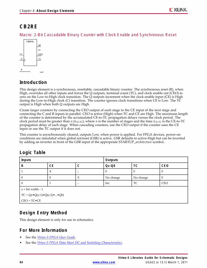
Chapter 4: About Design Elements
CB2REMacro: 2-Bit Cascadable Binary Counter with Clock Enable and Synchronous Reset
IntroductionThis design element is a synchronous, resettable, cascadable binary counter. The synchronous reset (R), whenHigh, overrides all other inputs and forces the Q outputs, terminal count (TC), and clock enable out (CEO) tozero on the Low-to-High clock transition. The Q outputs increment when the clock enable input (CE) is Highduring the Low-to-High clock (C) transition. The counter ignores clock transitions when CE is Low. The TCoutput is High when both Q outputs are High.
Create larger counters by connecting the CEO output of each stage to the CE input of the next stage andconnecting the C and R inputs in parallel. CEO is active (High) when TC and CE are High. The maximum lengthof the counter is determined by the accumulated CE-to-TC propagation delays versus the clock period. Theclock period must be greater than n (tCE-TC), where n is the number of stages and the time tCE-TC is the CE-to-TCpropagation delay of each stage. When cascading counters, use the CEO output if the counter uses the CEinput or use the TC output if it does not.
This counter is asynchronously cleared, outputs Low, when power is applied. For FPGA devices, power-onconditions are simulated when global set/reset (GSR) is active. GSR defaults to active-High but can be invertedby adding an inverter in front of the GSR input of the appropriate STARTUP_architecture symbol.
Logic TableInputs Outputs
R CE C Qz-Q0 TC CEO1 X ↑ 0 0 0
0 0 X No change No change 0
0 1 ↑ Inc TC CEO
z = bit width - 1
TC = Qz•Q(z-1)•Q(z-2)•...•Q0)
CEO = TC•CE
Design Entry MethodThis design element is only for use in schematics.
For More Information• See the Virtex-5 FPGA User Guide.• See the Virtex-5 FPGA Data Sheet DC and Switching Characteristics.
Virtex-5 Libraries Guide for Schematic Designs94 www.xilinx.com UG622 (v 13.1) March 1, 2011

Chapter 4: About Design Elements
CB4CEMacro: 4-Bit Cascadable Binary Counter with Clock Enable and Asynchronous Clear
IntroductionThis design element is an asynchronously clearable, cascadable binary counter. The asynchronous clear (CLR)input, when High, overrides all other inputs and forces the Q outputs, terminal count (TC), and clock enable out(CEO) to logic level zero, independent of clock transitions. The Q outputs increment when the clock enable input(CE) is High during the Low-to-High clock (C) transition. The counter ignores clock transitions when CE is Low.The TC output is High when all Q outputs are High.
Create larger counters by connecting the CEO output of each stage to the CE input of the next stage andconnecting the C and CLR inputs in parallel. CEO is active (High) when TC and CE are High. The maximumlength of the counter is determined by the accumulated CE-to-TC propagation delays versus the clock period.The clock period must be greater than n (tCE-TC), where n is the number of stages and the time tCE-TC is theCE-to-TC propagation delay of each stage. When cascading counters, use the CEO output if the counter uses theCE input or use the TC output if it does not.
This counter is asynchronously cleared, outputs Low, when power is applied. For FPGA devices, power-onconditions are simulated when global set/reset (GSR) is active. GSR defaults to active-High but can be invertedby adding an inverter in front of the GSR input of the appropriate STARTUP_architecture symbol.
Logic TableInputs Outputs
CLR CE C Qz-Q0 TC CEO1 X X 0 0 0
0 0 X No change No change 0
0 1 ↑ Inc TC CEO
z = bit width - 1
TC = Qz•Q(z-1)•Q(z-2)•...•Q0
CEO = TC•CE
Design Entry MethodThis design element is only for use in schematics.
For More Information• See the Virtex-5 FPGA User Guide.• See the Virtex-5 FPGA Data Sheet DC and Switching Characteristics.
Virtex-5 Libraries Guide for Schematic DesignsUG622 (v 13.1) March 1, 2011 www.xilinx.com 95

Chapter 4: About Design Elements
CB4CLEMacro: 4-Bit Loadable Cascadable Binary Counters with Clock Enable and AsynchronousClear
IntroductionThis element is a synchronously loadable, asynchronously clearable, cascadable binary counter. Theasynchronous clear (CLR) input, when High, overrides all other inputs and forces the Q outputs, terminalcount (TC), and clock enable out (CEO) to logic level zero, independent of clock transitions. The data on theD inputs is loaded into the counter when the load enable input (L) is High during the Low-to-High clocktransition, independent of the state of clock enable (CE). The Q outputs increment when CE is High during theLow-to-High clock transition. The counter ignores clock transitions when CE is Low. The TC output is Highwhen all Q outputs are High.
Create larger counters by connecting the CEO output of each stage to the CE input of the next stage andconnecting the C, L, and CLR inputs in parallel. CEO is active (High) when TC and CE are High. The maximumlength of the counter is determined by the accumulated CE-to-TC propagation delays versus the clock period.The clock period must be greater than n (tCE-TC), where n is the number of stages and the time tCE-TC is theCE-to-TC propagation delay of each stage. When cascading counters, use the CEO output if the counter uses theCE input or use the TC output if it does not.
This counter is asynchronously cleared, outputs Low, when power is applied. For FPGA devices, power-onconditions are simulated when global set/reset (GSR) is active. GSR defaults to active-High but can be invertedby adding an inverter in front of the GSR input of the appropriate STARTUP_architecture symbol.
Logic TableInputs Outputs
CLR L CE C Dz-D0 Qz-Q0 TC CEO1 X X X X 0 0 0
0 1 X ↑ Dn Dn TC CEO
0 0 0 X X No change No change 0
0 0 1 ↑ X Inc TC CEO
z = bit width - 1
TC = Qz•Q(z-1)•Q(z-2)•...•Q0
CEO = TC•CE
Virtex-5 Libraries Guide for Schematic Designs96 www.xilinx.com UG622 (v 13.1) March 1, 2011
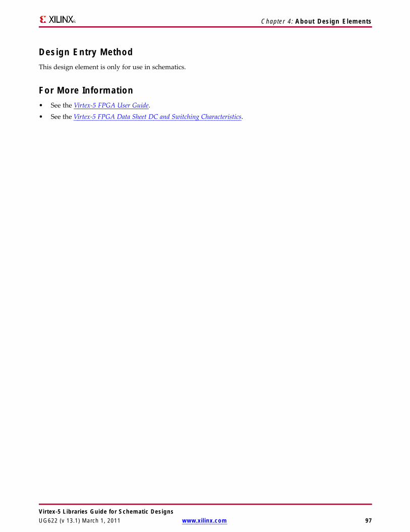
Chapter 4: About Design Elements
Design Entry MethodThis design element is only for use in schematics.
For More Information• See the Virtex-5 FPGA User Guide.
• See the Virtex-5 FPGA Data Sheet DC and Switching Characteristics.
Virtex-5 Libraries Guide for Schematic DesignsUG622 (v 13.1) March 1, 2011 www.xilinx.com 97
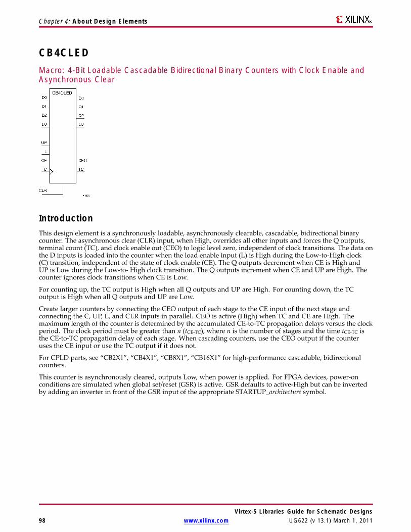
Chapter 4: About Design Elements
CB4CLEDMacro: 4-Bit Loadable Cascadable Bidirectional Binary Counters with Clock Enable andAsynchronous Clear
IntroductionThis design element is a synchronously loadable, asynchronously clearable, cascadable, bidirectional binarycounter. The asynchronous clear (CLR) input, when High, overrides all other inputs and forces the Q outputs,terminal count (TC), and clock enable out (CEO) to logic level zero, independent of clock transitions. The data onthe D inputs is loaded into the counter when the load enable input (L) is High during the Low-to-High clock(C) transition, independent of the state of clock enable (CE). The Q outputs decrement when CE is High andUP is Low during the Low-to- High clock transition. The Q outputs increment when CE and UP are High. Thecounter ignores clock transitions when CE is Low.
For counting up, the TC output is High when all Q outputs and UP are High. For counting down, the TCoutput is High when all Q outputs and UP are Low.
Create larger counters by connecting the CEO output of each stage to the CE input of the next stage andconnecting the C, UP, L, and CLR inputs in parallel. CEO is active (High) when TC and CE are High. Themaximum length of the counter is determined by the accumulated CE-to-TC propagation delays versus the clockperiod. The clock period must be greater than n (tCE-TC), where n is the number of stages and the time tCE-TC isthe CE-to-TC propagation delay of each stage. When cascading counters, use the CEO output if the counteruses the CE input or use the TC output if it does not.
For CPLD parts, see “CB2X1”, “CB4X1”, “CB8X1”, “CB16X1” for high-performance cascadable, bidirectionalcounters.
This counter is asynchronously cleared, outputs Low, when power is applied. For FPGA devices, power-onconditions are simulated when global set/reset (GSR) is active. GSR defaults to active-High but can be invertedby adding an inverter in front of the GSR input of the appropriate STARTUP_architecture symbol.
Virtex-5 Libraries Guide for Schematic Designs98 www.xilinx.com UG622 (v 13.1) March 1, 2011

Chapter 4: About Design Elements
Logic TableInputs Outputs
CLR L CE C UP Dz-D0 Qz-Q0 TC CEO1 X X X X X 0 0 0
0 1 X ↑ X Dn Dn TC CEO
0 0 0 X X X No change No change 0
0 0 1 ↑ 1 X Inc TC CEO
0 0 1 ↑ 0 X Dec TC CEO
z = bit width - 1
TC = (Qz•Q(z-1)•Q(z-2)•...•Q0•UP) + (Qz•Q(z-1)•Q(z-2)•...•Q0•UP)
CEO = TC•CE
Design Entry MethodThis design element is only for use in schematics.
For More Information• See the Virtex-5 FPGA User Guide.
• See the Virtex-5 FPGA Data Sheet DC and Switching Characteristics.
Virtex-5 Libraries Guide for Schematic DesignsUG622 (v 13.1) March 1, 2011 www.xilinx.com 99

Chapter 4: About Design Elements
CB4REMacro: 4-Bit Cascadable Binary Counter with Clock Enable and Synchronous Reset
IntroductionThis design element is a synchronous, resettable, cascadable binary counter. The synchronous reset (R), whenHigh, overrides all other inputs and forces the Q outputs, terminal count (TC), and clock enable out (CEO) tozero on the Low-to-High clock transition. The Q outputs increment when the clock enable input (CE) is Highduring the Low-to-High clock (C) transition. The counter ignores clock transitions when CE is Low. The TCoutput is High when both Q outputs are High.
Create larger counters by connecting the CEO output of each stage to the CE input of the next stage andconnecting the C and R inputs in parallel. CEO is active (High) when TC and CE are High. The maximum lengthof the counter is determined by the accumulated CE-to-TC propagation delays versus the clock period. Theclock period must be greater than n (tCE-TC), where n is the number of stages and the time tCE-TC is the CE-to-TCpropagation delay of each stage. When cascading counters, use the CEO output if the counter uses the CEinput or use the TC output if it does not.
This counter is asynchronously cleared, outputs Low, when power is applied. For FPGA devices, power-onconditions are simulated when global set/reset (GSR) is active. GSR defaults to active-High but can be invertedby adding an inverter in front of the GSR input of the appropriate STARTUP_architecture symbol.
Logic TableInputs Outputs
R CE C Qz-Q0 TC CEO1 X ↑ 0 0 0
0 0 X No change No change 0
0 1 ↑ Inc TC CEO
z = bit width - 1
TC = Qz•Q(z-1)•Q(z-2)•...•Q0)
CEO = TC•CE
Design Entry MethodThis design element is only for use in schematics.
For More Information• See the Virtex-5 FPGA User Guide.• See the Virtex-5 FPGA Data Sheet DC and Switching Characteristics.
Virtex-5 Libraries Guide for Schematic Designs100 www.xilinx.com UG622 (v 13.1) March 1, 2011

Chapter 4: About Design Elements
CB8CEMacro: 8-Bit Cascadable Binary Counter with Clock Enable and Asynchronous Clear
IntroductionThis design element is an asynchronously clearable, cascadable binary counter. The asynchronous clear (CLR)input, when High, overrides all other inputs and forces the Q outputs, terminal count (TC), and clock enable out(CEO) to logic level zero, independent of clock transitions. The Q outputs increment when the clock enable input(CE) is High during the Low-to-High clock (C) transition. The counter ignores clock transitions when CE is Low.The TC output is High when all Q outputs are High.
Create larger counters by connecting the CEO output of each stage to the CE input of the next stage andconnecting the C and CLR inputs in parallel. CEO is active (High) when TC and CE are High. The maximumlength of the counter is determined by the accumulated CE-to-TC propagation delays versus the clock period.The clock period must be greater than n (tCE-TC), where n is the number of stages and the time tCE-TC is theCE-to-TC propagation delay of each stage. When cascading counters, use the CEO output if the counter uses theCE input or use the TC output if it does not.
This counter is asynchronously cleared, outputs Low, when power is applied. For FPGA devices, power-onconditions are simulated when global set/reset (GSR) is active. GSR defaults to active-High but can be invertedby adding an inverter in front of the GSR input of the appropriate STARTUP_architecture symbol.
Logic TableInputs Outputs
CLR CE C Qz-Q0 TC CEO1 X X 0 0 0
0 0 X No change No change 0
0 1 ↑ Inc TC CEO
z = bit width - 1
TC = Qz•Q(z-1)•Q(z-2)•...•Q0
CEO = TC•CE
Design Entry MethodThis design element is only for use in schematics.
For More Information• See the Virtex-5 FPGA User Guide.• See the Virtex-5 FPGA Data Sheet DC and Switching Characteristics.
Virtex-5 Libraries Guide for Schematic DesignsUG622 (v 13.1) March 1, 2011 www.xilinx.com 101

Virtex-5 Libraries Guide for Schematic Designs102 www.xilinx.com UG622 (v 13.1) March 1, 2011

Chapter 4: About Design Elements
CB8CLEMacro: 8-Bit Loadable Cascadable Binary Counters with Clock Enable and AsynchronousClear
IntroductionThis element is a synchronously loadable, asynchronously clearable, cascadable binary counter. Theasynchronous clear (CLR) input, when High, overrides all other inputs and forces the Q outputs, terminalcount (TC), and clock enable out (CEO) to logic level zero, independent of clock transitions. The data on theD inputs is loaded into the counter when the load enable input (L) is High during the Low-to-High clocktransition, independent of the state of clock enable (CE). The Q outputs increment when CE is High during theLow-to-High clock transition. The counter ignores clock transitions when CE is Low. The TC output is Highwhen all Q outputs are High.
Create larger counters by connecting the CEO output of each stage to the CE input of the next stage andconnecting the C, L, and CLR inputs in parallel. CEO is active (High) when TC and CE are High. The maximumlength of the counter is determined by the accumulated CE-to-TC propagation delays versus the clock period.The clock period must be greater than n (tCE-TC), where n is the number of stages and the time tCE-TC is theCE-to-TC propagation delay of each stage. When cascading counters, use the CEO output if the counter uses theCE input or use the TC output if it does not.
This counter is asynchronously cleared, outputs Low, when power is applied. For FPGA devices, power-onconditions are simulated when global set/reset (GSR) is active. GSR defaults to active-High but can be invertedby adding an inverter in front of the GSR input of the appropriate STARTUP_architecture symbol.
Logic TableInputs Outputs
CLR L CE C Dz-D0 Qz-Q0 TC CEO1 X X X X 0 0 0
0 1 X ↑ Dn Dn TC CEO
0 0 0 X X No change No change 0
0 0 1 ↑ X Inc TC CEO
z = bit width - 1
TC = Qz•Q(z-1)•Q(z-2)•...•Q0
CEO = TC•CE
Design Entry MethodThis design element is only for use in schematics.
Virtex-5 Libraries Guide for Schematic DesignsUG622 (v 13.1) March 1, 2011 www.xilinx.com 103
Chapter 4: About Design Elements
For More Information• See the Virtex-5 FPGA User Guide.
• See the Virtex-5 FPGA Data Sheet DC and Switching Characteristics.
Virtex-5 Libraries Guide for Schematic Designs104 www.xilinx.com UG622 (v 13.1) March 1, 2011
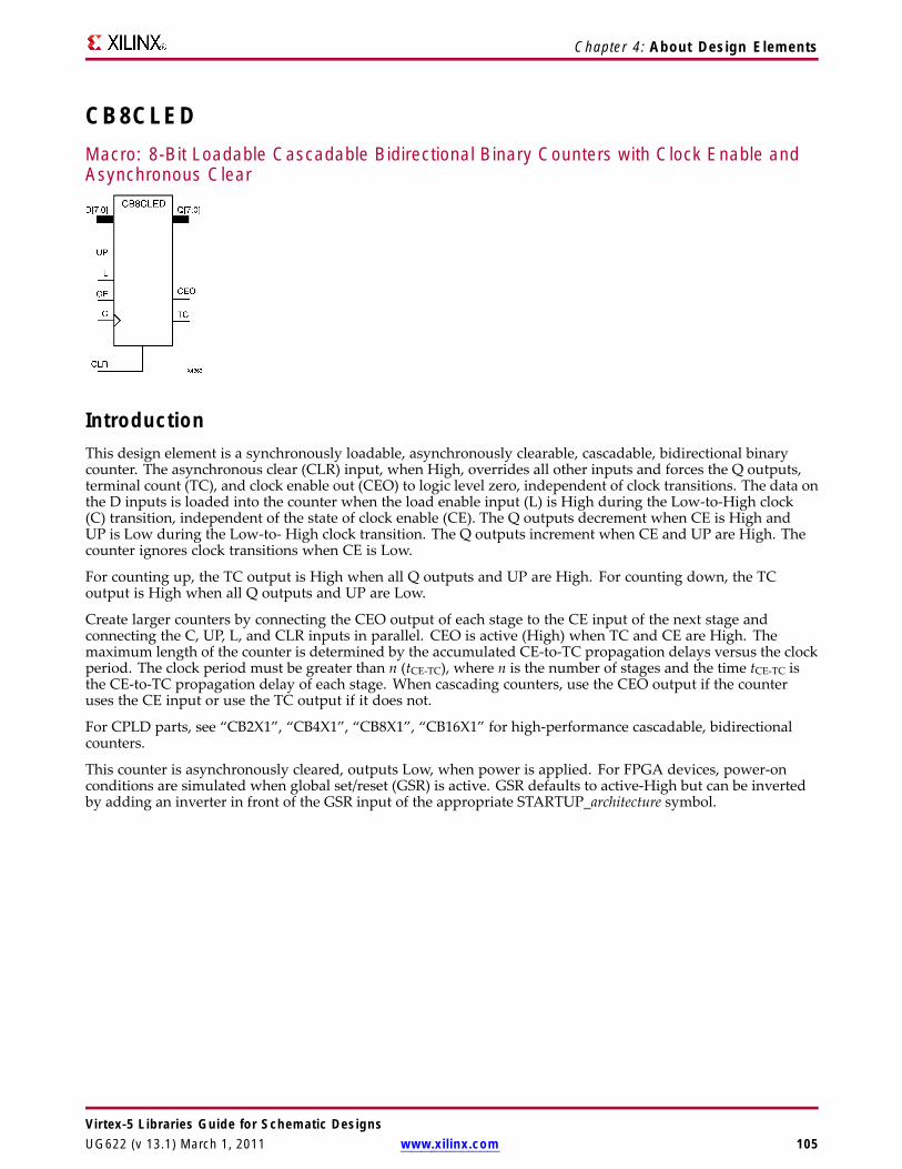
Chapter 4: About Design Elements
CB8CLEDMacro: 8-Bit Loadable Cascadable Bidirectional Binary Counters with Clock Enable andAsynchronous Clear
IntroductionThis design element is a synchronously loadable, asynchronously clearable, cascadable, bidirectional binarycounter. The asynchronous clear (CLR) input, when High, overrides all other inputs and forces the Q outputs,terminal count (TC), and clock enable out (CEO) to logic level zero, independent of clock transitions. The data onthe D inputs is loaded into the counter when the load enable input (L) is High during the Low-to-High clock(C) transition, independent of the state of clock enable (CE). The Q outputs decrement when CE is High andUP is Low during the Low-to- High clock transition. The Q outputs increment when CE and UP are High. Thecounter ignores clock transitions when CE is Low.
For counting up, the TC output is High when all Q outputs and UP are High. For counting down, the TCoutput is High when all Q outputs and UP are Low.
Create larger counters by connecting the CEO output of each stage to the CE input of the next stage andconnecting the C, UP, L, and CLR inputs in parallel. CEO is active (High) when TC and CE are High. Themaximum length of the counter is determined by the accumulated CE-to-TC propagation delays versus the clockperiod. The clock period must be greater than n (tCE-TC), where n is the number of stages and the time tCE-TC isthe CE-to-TC propagation delay of each stage. When cascading counters, use the CEO output if the counteruses the CE input or use the TC output if it does not.
For CPLD parts, see “CB2X1”, “CB4X1”, “CB8X1”, “CB16X1” for high-performance cascadable, bidirectionalcounters.
This counter is asynchronously cleared, outputs Low, when power is applied. For FPGA devices, power-onconditions are simulated when global set/reset (GSR) is active. GSR defaults to active-High but can be invertedby adding an inverter in front of the GSR input of the appropriate STARTUP_architecture symbol.
Virtex-5 Libraries Guide for Schematic DesignsUG622 (v 13.1) March 1, 2011 www.xilinx.com 105
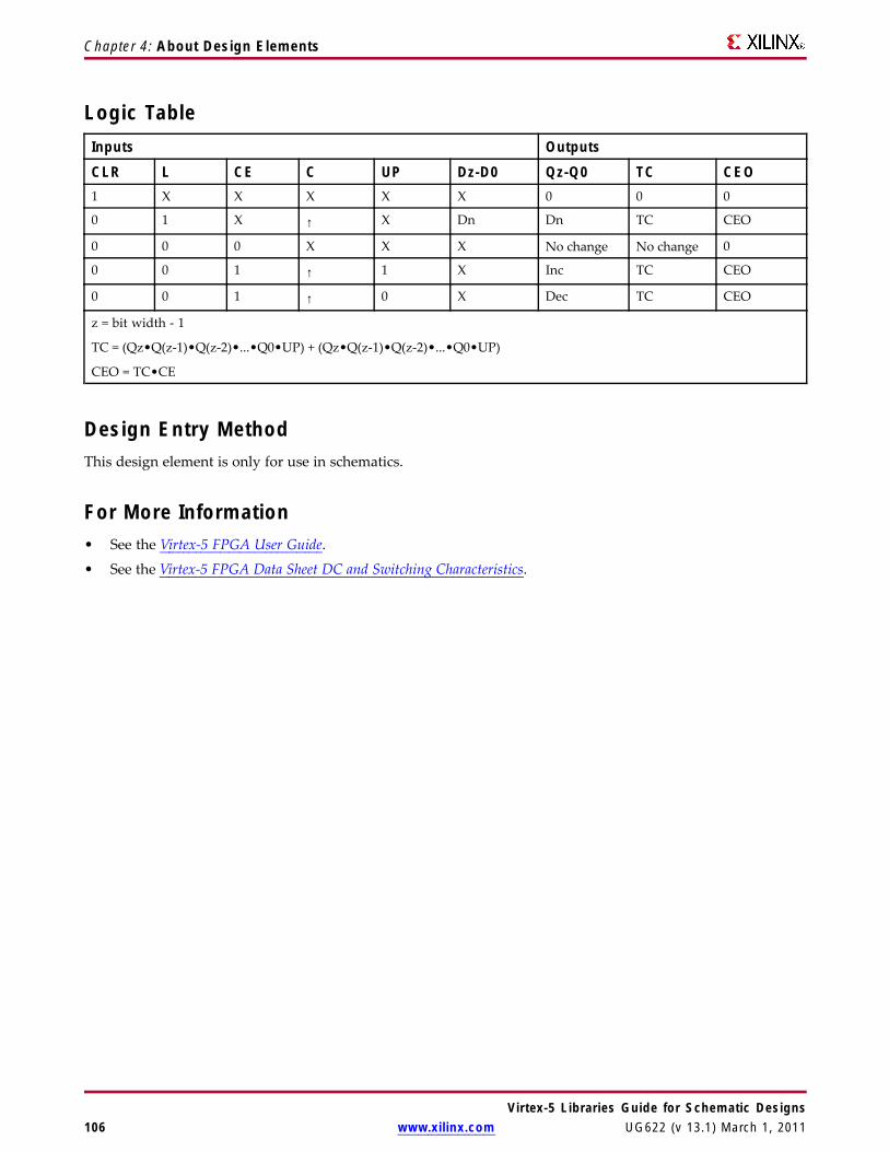
Chapter 4: About Design Elements
Logic TableInputs Outputs
CLR L CE C UP Dz-D0 Qz-Q0 TC CEO1 X X X X X 0 0 0
0 1 X ↑ X Dn Dn TC CEO
0 0 0 X X X No change No change 0
0 0 1 ↑ 1 X Inc TC CEO
0 0 1 ↑ 0 X Dec TC CEO
z = bit width - 1
TC = (Qz•Q(z-1)•Q(z-2)•...•Q0•UP) + (Qz•Q(z-1)•Q(z-2)•...•Q0•UP)
CEO = TC•CE
Design Entry MethodThis design element is only for use in schematics.
For More Information• See the Virtex-5 FPGA User Guide.
• See the Virtex-5 FPGA Data Sheet DC and Switching Characteristics.
Virtex-5 Libraries Guide for Schematic Designs106 www.xilinx.com UG622 (v 13.1) March 1, 2011

Chapter 4: About Design Elements
CB8REMacro: 8-Bit Cascadable Binary Counter with Clock Enable and Synchronous Reset
IntroductionThis design element is a synchronous, resettable, cascadable binary counter. The synchronous reset (R), whenHigh, overrides all other inputs and forces the Q outputs, terminal count (TC), and clock enable out (CEO) tozero on the Low-to-High clock transition. The Q outputs increment when the clock enable input (CE) is Highduring the Low-to-High clock (C) transition. The counter ignores clock transitions when CE is Low. The TCoutput is High when both Q outputs are High.
Create larger counters by connecting the CEO output of each stage to the CE input of the next stage andconnecting the C and R inputs in parallel. CEO is active (High) when TC and CE are High. The maximum lengthof the counter is determined by the accumulated CE-to-TC propagation delays versus the clock period. Theclock period must be greater than n (tCE-TC), where n is the number of stages and the time tCE-TC is the CE-to-TCpropagation delay of each stage. When cascading counters, use the CEO output if the counter uses the CEinput or use the TC output if it does not.
This counter is asynchronously cleared, outputs Low, when power is applied. For FPGA devices, power-onconditions are simulated when global set/reset (GSR) is active. GSR defaults to active-High but can be invertedby adding an inverter in front of the GSR input of the appropriate STARTUP_architecture symbol.
Logic TableInputs Outputs
R CE C Qz-Q0 TC CEO1 X ↑ 0 0 0
0 0 X No change No change 0
0 1 ↑ Inc TC CEO
z = bit width - 1
TC = Qz•Q(z-1)•Q(z-2)•...•Q0)
CEO = TC•CE
Design Entry MethodThis design element is only for use in schematics.
For More Information• See the Virtex-5 FPGA User Guide.• See the Virtex-5 FPGA Data Sheet DC and Switching Characteristics.
Virtex-5 Libraries Guide for Schematic DesignsUG622 (v 13.1) March 1, 2011 www.xilinx.com 107
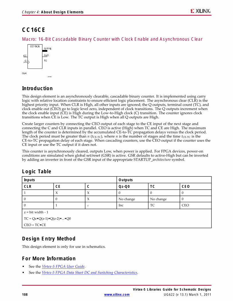
Chapter 4: About Design Elements
CC16CEMacro: 16-Bit Cascadable Binary Counter with Clock Enable and Asynchronous Clear
IntroductionThis design element is an asynchronously clearable, cascadable binary counter. It is implemented using carrylogic with relative location constraints to ensure efficient logic placement. The asynchronous clear (CLR) is thehighest priority input. When CLR is High, all other inputs are ignored; the Q outputs, terminal count (TC), andclock enable out (CEO) go to logic level zero, independent of clock transitions. The Q outputs increment whenthe clock enable input (CE) is High during the Low-to-High clock (C) transition. The counter ignores clocktransitions when CE is Low. The TC output is High when all Q outputs are High.
Create larger counters by connecting the CEO output of each stage to the CE input of the next stage andconnecting the C and CLR inputs in parallel. CEO is active (High) when TC and CE are High. The maximumlength of the counter is determined by the accumulated CE-to-TC propagation delays versus the clock period.The clock period must be greater than n (tCE-TC), where n is the number of stages and the time tCE-TC is theCE-to-TC propagation delay of each stage. When cascading counters, use the CEO output if the counter uses theCE input or use the TC output if it does not.
This counter is asynchronously cleared, outputs Low, when power is applied. For FPGA devices, power-onconditions are simulated when global set/reset (GSR) is active. GSR defaults to active-High but can be invertedby adding an inverter in front of the GSR input of the appropriate STARTUP_architecture symbol.
Logic TableInputs Outputs
CLR CE C Qz-Q0 TC CEO1 X X 0 0 0
0 0 X No change No change 0
0 1 ↑ Inc TC CEO
z = bit width - 1
TC = Qz•Q(z-1)•Q(z-2)•...•Q0
CEO = TC•CE
Design Entry MethodThis design element is only for use in schematics.
For More Information• See the Virtex-5 FPGA User Guide.• See the Virtex-5 FPGA Data Sheet DC and Switching Characteristics.
Virtex-5 Libraries Guide for Schematic Designs108 www.xilinx.com UG622 (v 13.1) March 1, 2011

Chapter 4: About Design Elements
CC16CLEMacro: 16-Bit Loadable Cascadable Binary Counter with Clock Enable and AsynchronousClear
IntroductionThis design element is a synchronously loadable, asynchronously clearable, cascadable binary counter. It isimplemented using carry logic with relative location constraints to ensure efficient logic placement. Theasynchronous clear (CLR) is the highest priority input. When CLR is High, all other inputs are ignored;the Q outputs, terminal count (TC), and clock enable out (CEO) go to logic level zero, independent of clocktransitions. The data on the D inputs is loaded into the counter when the load enable input (L) is High during theLow-to-High clock (C) transition, independent of the state of clock enable (CE). The Q outputs increment whenCE is High during the Low-to-High clock transition. The counter ignores clock transitions when CE is Low.The TC output is High when all Q outputs are High.
Create larger counters by connecting the CEO output of each stage to the CE input of the next stage andconnecting the C, L, and CLR inputs in parallel. CEO is active (High) when TC and CE are High. The maximumlength of the counter is determined by the accumulated CE-to-TC propagation delays versus the clock period.The clock period must be greater than n (tCE-TC), where n is the number of stages and the time tCE-TC is theCE-to-TC propagation delay of each stage. When cascading counters, use the CEO output if the counter uses theCE input or use the TC output if it does not.
This counter is asynchronously cleared, outputs Low, when power is applied. For FPGA devices, power-onconditions are simulated when global set/reset (GSR) is active. GSR defaults to active-High but can be invertedby adding an inverter in front of the GSR input of the appropriate STARTUP_architecture symbol.
Logic TableInputs Outputs
CLR L CE C Dz-D0 Qz-Q0 TC CEO1 X X X X 0 0 0
0 1 X ↑ Dn Dn TC CEO
0 0 0 X X No change No change 0
0 0 1 ↑ X Inc TC CEO
z = bit width - 1
TC = Qz•Q(z-1)•Q(z-2)•...•Q0
CEO = TC•CE
Design Entry MethodThis design element is only for use in schematics.
Virtex-5 Libraries Guide for Schematic DesignsUG622 (v 13.1) March 1, 2011 www.xilinx.com 109

Chapter 4: About Design Elements
For More Information• See the Virtex-5 FPGA User Guide.
• See the Virtex-5 FPGA Data Sheet DC and Switching Characteristics.
Virtex-5 Libraries Guide for Schematic Designs110 www.xilinx.com UG622 (v 13.1) March 1, 2011
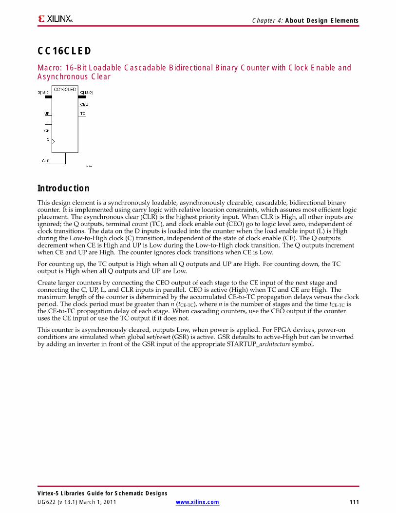
Chapter 4: About Design Elements
CC16CLEDMacro: 16-Bit Loadable Cascadable Bidirectional Binary Counter with Clock Enable andAsynchronous Clear
IntroductionThis design element is a synchronously loadable, asynchronously clearable, cascadable, bidirectional binarycounter. It is implemented using carry logic with relative location constraints, which assures most efficient logicplacement. The asynchronous clear (CLR) is the highest priority input. When CLR is High, all other inputs areignored; the Q outputs, terminal count (TC), and clock enable out (CEO) go to logic level zero, independent ofclock transitions. The data on the D inputs is loaded into the counter when the load enable input (L) is Highduring the Low-to-High clock (C) transition, independent of the state of clock enable (CE). The Q outputsdecrement when CE is High and UP is Low during the Low-to-High clock transition. The Q outputs incrementwhen CE and UP are High. The counter ignores clock transitions when CE is Low.
For counting up, the TC output is High when all Q outputs and UP are High. For counting down, the TCoutput is High when all Q outputs and UP are Low.
Create larger counters by connecting the CEO output of each stage to the CE input of the next stage andconnecting the C, UP, L, and CLR inputs in parallel. CEO is active (High) when TC and CE are High. Themaximum length of the counter is determined by the accumulated CE-to-TC propagation delays versus the clockperiod. The clock period must be greater than n (tCE-TC), where n is the number of stages and the time tCE-TC isthe CE-to-TC propagation delay of each stage. When cascading counters, use the CEO output if the counteruses the CE input or use the TC output if it does not.
This counter is asynchronously cleared, outputs Low, when power is applied. For FPGA devices, power-onconditions are simulated when global set/reset (GSR) is active. GSR defaults to active-High but can be invertedby adding an inverter in front of the GSR input of the appropriate STARTUP_architecture symbol.
Virtex-5 Libraries Guide for Schematic DesignsUG622 (v 13.1) March 1, 2011 www.xilinx.com 111

Chapter 4: About Design Elements
Logic TableInputs Outputs
CLR L CE C UP Dz-D0 Qz-Q0 TC CEO1 X X X X X 0 0 0
0 1 X ↑ X Dn Dn TC CEO
0 0 0 X X X No change No change 0
0 0 1 ↑ 1 X Inc TC CEO
0 0 1 ↑ 0 X Dec TC CEO
z = bit width - 1
TC = (Qz•Q(z-1)•Q(z-2)•...•Q0•UP) + (Qz•Q(z-1)•Q(z-2)•...•Q0•UP)
CEO = TC•CE
Design Entry MethodThis design element is only for use in schematics.
For More Information• See the Virtex-5 FPGA User Guide.
• See the Virtex-5 FPGA Data Sheet DC and Switching Characteristics.
Virtex-5 Libraries Guide for Schematic Designs112 www.xilinx.com UG622 (v 13.1) March 1, 2011

Chapter 4: About Design Elements
CC16REMacro: 16-Bit Cascadable Binary Counter with Clock Enable and Synchronous Reset
IntroductionThis design element is a synchronous resettable, cascadable binary counter. These counters are implementedusing carry logic with relative location constraints to ensure efficient logic placement. The synchronous reset(R) is the highest priority input. When R is High, all other inputs are ignored; the Q outputs, terminal count(TC), and clock enable out (CEO) go to logic level zero on the Low-to-High clock (C) transition. The Q outputsincrement when the clock enable input (CE) is High during the Low-to-High clock transition. The counterignores clock transitions when CE is Low. The TC output is High when all Q outputs and CE are High.
Create larger counters by connecting the CEO output of each stage to the CE input of the next stage andconnecting the C and R inputs in parallel. CEO is active (High) when TC and CE are High. The maximum lengthof the counter is determined by the accumulated CE-to-TC propagation delays versus the clock period. Theclock period must be greater than n (tCE-TC), where n is the number of stages and the time tCE-TC is the CE-to-TCpropagation delay of each stage. When cascading counters, use the CEO output if the counter uses the CEinput or use the TC output if it does not.
This counter is asynchronously cleared, outputs Low, when power is applied. For FPGA devices, power-onconditions are simulated when global set/reset (GSR) is active. GSR defaults to active-High but can be invertedby adding an inverter in front of the GSR input of the appropriate STARTUP_architecture symbol.
Logic TableInputs Outputs
R CE C Qz-Q0 TC CEO1 X ↑ 0 0 0
0 0 X No change No change 0
0 1 ↑ Inc TC CEO
z = bit width - 1
TC = Qz•Q(z-1)•Q(z-2)•...•Q0)
CEO = TC•CE
Design Entry MethodThis design element is only for use in schematics.
For More Information• See the Virtex-5 FPGA User Guide.• See the Virtex-5 FPGA Data Sheet DC and Switching Characteristics.
Virtex-5 Libraries Guide for Schematic DesignsUG622 (v 13.1) March 1, 2011 www.xilinx.com 113

Chapter 4: About Design Elements
CC8CEMacro: 8-Bit Cascadable Binary Counter with Clock Enable and Asynchronous Clear
IntroductionThis design element is an asynchronously clearable, cascadable binary counter. It is implemented using carrylogic with relative location constraints to ensure efficient logic placement. The asynchronous clear (CLR) is thehighest priority input. When CLR is High, all other inputs are ignored; the Q outputs, terminal count (TC), andclock enable out (CEO) go to logic level zero, independent of clock transitions. The Q outputs increment whenthe clock enable input (CE) is High during the Low-to-High clock (C) transition. The counter ignores clocktransitions when CE is Low. The TC output is High when all Q outputs are High.
Create larger counters by connecting the CEO output of each stage to the CE input of the next stage andconnecting the C and CLR inputs in parallel. CEO is active (High) when TC and CE are High. The maximumlength of the counter is determined by the accumulated CE-to-TC propagation delays versus the clock period.The clock period must be greater than n (tCE-TC), where n is the number of stages and the time tCE-TC is theCE-to-TC propagation delay of each stage. When cascading counters, use the CEO output if the counter uses theCE input or use the TC output if it does not.
This counter is asynchronously cleared, outputs Low, when power is applied. For FPGA devices, power-onconditions are simulated when global set/reset (GSR) is active. GSR defaults to active-High but can be invertedby adding an inverter in front of the GSR input of the appropriate STARTUP_architecture symbol.
Logic TableInputs Outputs
CLR CE C Qz-Q0 TC CEO1 X X 0 0 0
0 0 X No change No change 0
0 1 ↑ Inc TC CEO
z = bit width - 1
TC = Qz•Q(z-1)•Q(z-2)•...•Q0
CEO = TC•CE
Design Entry MethodThis design element is only for use in schematics.
For More Information• See the Virtex-5 FPGA User Guide.• See the Virtex-5 FPGA Data Sheet DC and Switching Characteristics.
Virtex-5 Libraries Guide for Schematic Designs114 www.xilinx.com UG622 (v 13.1) March 1, 2011
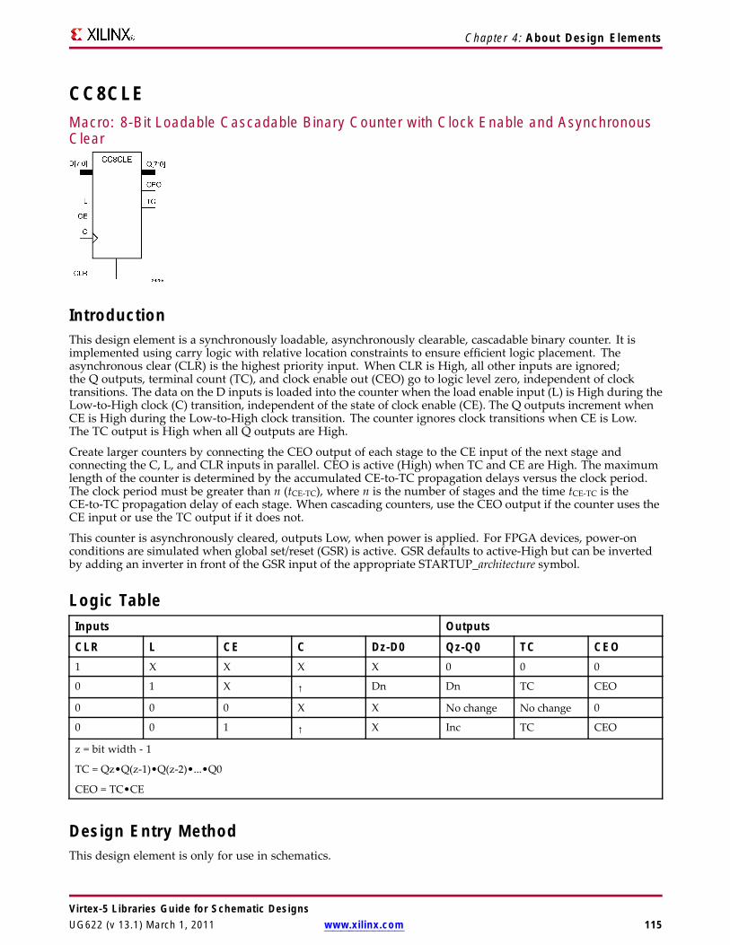
Chapter 4: About Design Elements
CC8CLEMacro: 8-Bit Loadable Cascadable Binary Counter with Clock Enable and AsynchronousClear
IntroductionThis design element is a synchronously loadable, asynchronously clearable, cascadable binary counter. It isimplemented using carry logic with relative location constraints to ensure efficient logic placement. Theasynchronous clear (CLR) is the highest priority input. When CLR is High, all other inputs are ignored;the Q outputs, terminal count (TC), and clock enable out (CEO) go to logic level zero, independent of clocktransitions. The data on the D inputs is loaded into the counter when the load enable input (L) is High during theLow-to-High clock (C) transition, independent of the state of clock enable (CE). The Q outputs increment whenCE is High during the Low-to-High clock transition. The counter ignores clock transitions when CE is Low.The TC output is High when all Q outputs are High.
Create larger counters by connecting the CEO output of each stage to the CE input of the next stage andconnecting the C, L, and CLR inputs in parallel. CEO is active (High) when TC and CE are High. The maximumlength of the counter is determined by the accumulated CE-to-TC propagation delays versus the clock period.The clock period must be greater than n (tCE-TC), where n is the number of stages and the time tCE-TC is theCE-to-TC propagation delay of each stage. When cascading counters, use the CEO output if the counter uses theCE input or use the TC output if it does not.
This counter is asynchronously cleared, outputs Low, when power is applied. For FPGA devices, power-onconditions are simulated when global set/reset (GSR) is active. GSR defaults to active-High but can be invertedby adding an inverter in front of the GSR input of the appropriate STARTUP_architecture symbol.
Logic TableInputs Outputs
CLR L CE C Dz-D0 Qz-Q0 TC CEO1 X X X X 0 0 0
0 1 X ↑ Dn Dn TC CEO
0 0 0 X X No change No change 0
0 0 1 ↑ X Inc TC CEO
z = bit width - 1
TC = Qz•Q(z-1)•Q(z-2)•...•Q0
CEO = TC•CE
Design Entry MethodThis design element is only for use in schematics.
Virtex-5 Libraries Guide for Schematic DesignsUG622 (v 13.1) March 1, 2011 www.xilinx.com 115

Chapter 4: About Design Elements
For More Information• See the Virtex-5 FPGA User Guide.
• See the Virtex-5 FPGA Data Sheet DC and Switching Characteristics.
Virtex-5 Libraries Guide for Schematic Designs116 www.xilinx.com UG622 (v 13.1) March 1, 2011

Chapter 4: About Design Elements
CC8CLEDMacro: 8-Bit Loadable Cascadable Bidirectional Binary Counter with Clock Enable andAsynchronous Clear
IntroductionThis design element is a synchronously loadable, asynchronously clearable, cascadable, bidirectional binarycounter. It is implemented using carry logic with relative location constraints, which assures most efficient logicplacement. The asynchronous clear (CLR) is the highest priority input. When CLR is High, all other inputs areignored; the Q outputs, terminal count (TC), and clock enable out (CEO) go to logic level zero, independent ofclock transitions. The data on the D inputs is loaded into the counter when the load enable input (L) is Highduring the Low-to-High clock (C) transition, independent of the state of clock enable (CE). The Q outputsdecrement when CE is High and UP is Low during the Low-to-High clock transition. The Q outputs incrementwhen CE and UP are High. The counter ignores clock transitions when CE is Low.
For counting up, the TC output is High when all Q outputs and UP are High. For counting down, the TCoutput is High when all Q outputs and UP are Low.
Create larger counters by connecting the CEO output of each stage to the CE input of the next stage andconnecting the C, UP, L, and CLR inputs in parallel. CEO is active (High) when TC and CE are High. Themaximum length of the counter is determined by the accumulated CE-to-TC propagation delays versus the clockperiod. The clock period must be greater than n (tCE-TC), where n is the number of stages and the time tCE-TC isthe CE-to-TC propagation delay of each stage. When cascading counters, use the CEO output if the counteruses the CE input or use the TC output if it does not.
This counter is asynchronously cleared, outputs Low, when power is applied. For FPGA devices, power-onconditions are simulated when global set/reset (GSR) is active. GSR defaults to active-High but can be invertedby adding an inverter in front of the GSR input of the appropriate STARTUP_architecture symbol.
Virtex-5 Libraries Guide for Schematic DesignsUG622 (v 13.1) March 1, 2011 www.xilinx.com 117

Chapter 4: About Design Elements
Logic TableInputs Outputs
CLR L CE C UP Dz-D0 Qz-Q0 TC CEO1 X X X X X 0 0 0
0 1 X ↑ X Dn Dn TC CEO
0 0 0 X X X No change No change 0
0 0 1 ↑ 1 X Inc TC CEO
0 0 1 ↑ 0 X Dec TC CEO
z = bit width - 1
TC = (Qz•Q(z-1)•Q(z-2)•...•Q0•UP) + (Qz•Q(z-1)•Q(z-2)•...•Q0•UP)
CEO = TC•CE
Design Entry MethodThis design element is only for use in schematics.
For More Information• See the Virtex-5 FPGA User Guide.
• See the Virtex-5 FPGA Data Sheet DC and Switching Characteristics.
Virtex-5 Libraries Guide for Schematic Designs118 www.xilinx.com UG622 (v 13.1) March 1, 2011
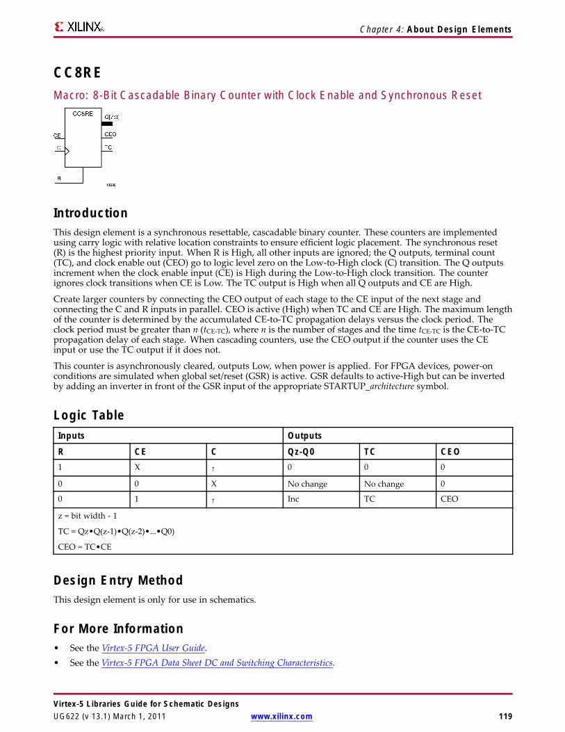
Chapter 4: About Design Elements
CC8REMacro: 8-Bit Cascadable Binary Counter with Clock Enable and Synchronous Reset
IntroductionThis design element is a synchronous resettable, cascadable binary counter. These counters are implementedusing carry logic with relative location constraints to ensure efficient logic placement. The synchronous reset(R) is the highest priority input. When R is High, all other inputs are ignored; the Q outputs, terminal count(TC), and clock enable out (CEO) go to logic level zero on the Low-to-High clock (C) transition. The Q outputsincrement when the clock enable input (CE) is High during the Low-to-High clock transition. The counterignores clock transitions when CE is Low. The TC output is High when all Q outputs and CE are High.
Create larger counters by connecting the CEO output of each stage to the CE input of the next stage andconnecting the C and R inputs in parallel. CEO is active (High) when TC and CE are High. The maximum lengthof the counter is determined by the accumulated CE-to-TC propagation delays versus the clock period. Theclock period must be greater than n (tCE-TC), where n is the number of stages and the time tCE-TC is the CE-to-TCpropagation delay of each stage. When cascading counters, use the CEO output if the counter uses the CEinput or use the TC output if it does not.
This counter is asynchronously cleared, outputs Low, when power is applied. For FPGA devices, power-onconditions are simulated when global set/reset (GSR) is active. GSR defaults to active-High but can be invertedby adding an inverter in front of the GSR input of the appropriate STARTUP_architecture symbol.
Logic TableInputs Outputs
R CE C Qz-Q0 TC CEO1 X ↑ 0 0 0
0 0 X No change No change 0
0 1 ↑ Inc TC CEO
z = bit width - 1
TC = Qz•Q(z-1)•Q(z-2)•...•Q0)
CEO = TC•CE
Design Entry MethodThis design element is only for use in schematics.
For More Information• See the Virtex-5 FPGA User Guide.• See the Virtex-5 FPGA Data Sheet DC and Switching Characteristics.
Virtex-5 Libraries Guide for Schematic DesignsUG622 (v 13.1) March 1, 2011 www.xilinx.com 119

Chapter 4: About Design Elements
CD4CEMacro: 4-Bit Cascadable BCD Counter with Clock Enable and Asynchronous Clear
IntroductionCD4CE is a 4-bit (stage), asynchronous clearable, cascadable binary-coded-decimal (BCD) counter. Theasynchronous clear input (CLR) is the highest priority input. When CLR is High, all other inputs are ignored;the Q outputs, terminal count (TC), and clock enable out (CEO) go to logic level zero, independent of clocktransitions. The Q outputs increment when clock enable (CE) is High during the Low-to-High clock (C)transition. The counter ignores clock transitions when CE is Low. The TC output is High when Q3 and Q0 areHigh and Q2 and Q1 are Low.
The counter recovers from any of six possible illegal states and returns to a normal count sequence within twoclock cycles for Xilinx® devices, as shown in the following state diagram:
Create larger counters by connecting the CEO output of each stage to the CE input of the next stage andconnecting the C and CLR inputs in parallel. CEO is active (High) when TC and CE are High. The maximumlength of the counter is determined by the accumulated CE-to-TC propagation delays versus the clock period.The clock period must be greater than n (tCE-TC), where n is the number of stages and the time tCE-TC is theCE-to-TC propagation delay of each stage. When cascading counters, use the CEO output if the counter uses theCE input or use the TC output if it does not.
This counter is asynchronously cleared, outputs Low, when power is applied. For FPGA devices, power-onconditions are simulated when global set/reset (GSR) is active. GSR defaults to active-High but can be invertedby adding an inverter in front of the GSR input of the appropriate STARTUP_architecture symbol.
Virtex-5 Libraries Guide for Schematic Designs120 www.xilinx.com UG622 (v 13.1) March 1, 2011
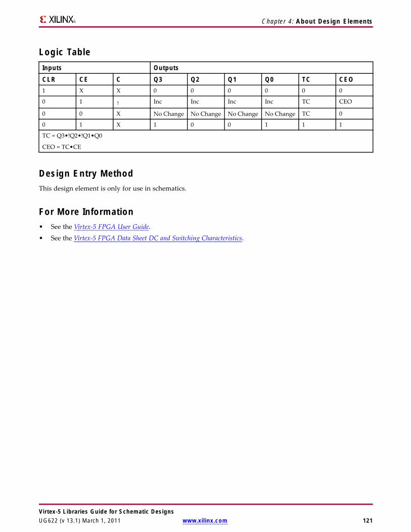
Chapter 4: About Design Elements
Logic TableInputs Outputs
CLR CE C Q3 Q2 Q1 Q0 TC CEO1 X X 0 0 0 0 0 0
0 1 ↑ Inc Inc Inc Inc TC CEO
0 0 X No Change No Change No Change No Change TC 0
0 1 X 1 0 0 1 1 1
TC = Q3•!Q2•!Q1•Q0
CEO = TC•CE
Design Entry MethodThis design element is only for use in schematics.
For More Information• See the Virtex-5 FPGA User Guide.
• See the Virtex-5 FPGA Data Sheet DC and Switching Characteristics.
Virtex-5 Libraries Guide for Schematic DesignsUG622 (v 13.1) March 1, 2011 www.xilinx.com 121
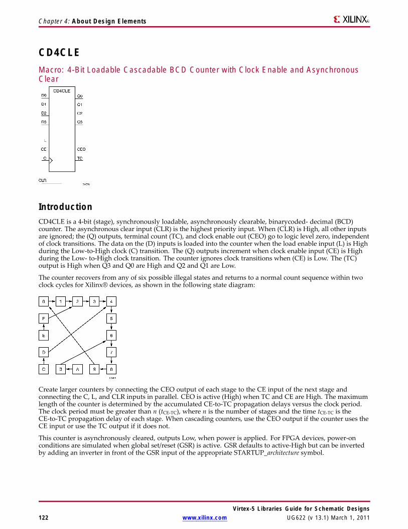
Chapter 4: About Design Elements
CD4CLEMacro: 4-Bit Loadable Cascadable BCD Counter with Clock Enable and AsynchronousClear
IntroductionCD4CLE is a 4-bit (stage), synchronously loadable, asynchronously clearable, binarycoded- decimal (BCD)counter. The asynchronous clear input (CLR) is the highest priority input. When (CLR) is High, all other inputsare ignored; the (Q) outputs, terminal count (TC), and clock enable out (CEO) go to logic level zero, independentof clock transitions. The data on the (D) inputs is loaded into the counter when the load enable input (L) is Highduring the Low-to-High clock (C) transition. The (Q) outputs increment when clock enable input (CE) is Highduring the Low- to-High clock transition. The counter ignores clock transitions when (CE) is Low. The (TC)output is High when Q3 and Q0 are High and Q2 and Q1 are Low.
The counter recovers from any of six possible illegal states and returns to a normal count sequence within twoclock cycles for Xilinx® devices, as shown in the following state diagram:
Create larger counters by connecting the CEO output of each stage to the CE input of the next stage andconnecting the C, L, and CLR inputs in parallel. CEO is active (High) when TC and CE are High. The maximumlength of the counter is determined by the accumulated CE-to-TC propagation delays versus the clock period.The clock period must be greater than n (tCE-TC), where n is the number of stages and the time tCE-TC is theCE-to-TC propagation delay of each stage. When cascading counters, use the CEO output if the counter uses theCE input or use the TC output if it does not.
This counter is asynchronously cleared, outputs Low, when power is applied. For FPGA devices, power-onconditions are simulated when global set/reset (GSR) is active. GSR defaults to active-High but can be invertedby adding an inverter in front of the GSR input of the appropriate STARTUP_architecture symbol.
Virtex-5 Libraries Guide for Schematic Designs122 www.xilinx.com UG622 (v 13.1) March 1, 2011

Chapter 4: About Design Elements
Logic TableInputs Outputs
CLR L CE D3 : D0 C Q3 Q2 Q1 Q0 TC CEO1 X X X X 0 0 0 0 0 0
0 1 X D3 : D0 ↑ D3 D2 D1 D0 TC CEO
0 0 1 X ↑ Inc Inc Inc Inc TC CEO
0 0 0 X X NoChange
NoChange
NoChange
NoChange
TC 0
0 0 1 X X 1 0 0 1 1 1
TC = Q3•!Q2•!Q1•Q0
CEO = TC•CE
Design Entry MethodThis design element is only for use in schematics.
For More Information• See the Virtex-5 FPGA User Guide.
• See the Virtex-5 FPGA Data Sheet DC and Switching Characteristics.
Virtex-5 Libraries Guide for Schematic DesignsUG622 (v 13.1) March 1, 2011 www.xilinx.com 123
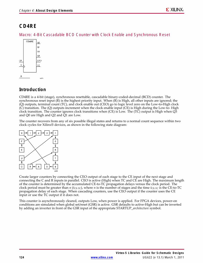
Chapter 4: About Design Elements
CD4REMacro: 4-Bit Cascadable BCD Counter with Clock Enable and Synchronous Reset
IntroductionCD4RE is a 4-bit (stage), synchronous resettable, cascadable binary-coded-decimal (BCD) counter. Thesynchronous reset input (R) is the highest priority input. When (R) is High, all other inputs are ignored; the(Q) outputs, terminal count (TC), and clock enable out (CEO) go to logic level zero on the Low-to-High clock(C) transition. The (Q) outputs increment when the clock enable input (CE) is High during the Low-to- Highclock transition. The counter ignores clock transitions when (CE) is Low. The (TC) output is High when Q3and Q0 are High and Q2 and Q1 are Low.
The counter recovers from any of six possible illegal states and returns to a normal count sequence within twoclock cycles for Xilinx® devices, as shown in the following state diagram:
Create larger counters by connecting the CEO output of each stage to the CE input of the next stage andconnecting the C and R inputs in parallel. CEO is active (High) when TC and CE are High. The maximum lengthof the counter is determined by the accumulated CE-to-TC propagation delays versus the clock period. Theclock period must be greater than n (tCE-TC), where n is the number of stages and the time tCE-TC is the CE-to-TCpropagation delay of each stage. When cascading counters, use the CEO output if the counter uses the CEinput or use the TC output if it does not.
This counter is asynchronously cleared, outputs Low, when power is applied. For FPGA devices, power-onconditions are simulated when global set/reset (GSR) is active. GSR defaults to active-High but can be invertedby adding an inverter in front of the GSR input of the appropriate STARTUP_architecture symbol.
Virtex-5 Libraries Guide for Schematic Designs124 www.xilinx.com UG622 (v 13.1) March 1, 2011

Chapter 4: About Design Elements
Logic TableInputs Outputs
R CE C Q3 Q2 Q1 Q0 TC CEO1 X ↑ 0 0 0 0 0 0
0 1 ↑ Inc Inc Inc Inc TC CEO
0 0 X No Change No Change No Change No Change TC 0
0 1 X 1 0 0 1 1 1
TC = Q3•!Q2•!Q1•Q0
CEO = TC•CE
Design Entry MethodThis design element is only for use in schematics.
For More Information• See the Virtex-5 FPGA User Guide.
• See the Virtex-5 FPGA Data Sheet DC and Switching Characteristics.
Virtex-5 Libraries Guide for Schematic DesignsUG622 (v 13.1) March 1, 2011 www.xilinx.com 125
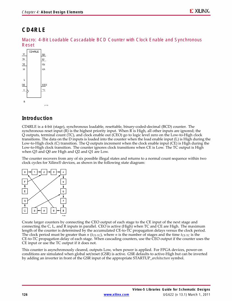
Chapter 4: About Design Elements
CD4RLEMacro: 4-Bit Loadable Cascadable BCD Counter with Clock Enable and SynchronousReset
IntroductionCD4RLE is a 4-bit (stage), synchronous loadable, resettable, binary-coded-decimal (BCD) counter. Thesynchronous reset input (R) is the highest priority input. When R is High, all other inputs are ignored; theQ outputs, terminal count (TC), and clock enable out (CEO) go to logic level zero on the Low-to-High clocktransitions. The data on the D inputs is loaded into the counter when the load enable input (L) is High during theLow-to-High clock (C) transition. The Q outputs increment when the clock enable input (CE) is High during theLow-to-High clock transition. The counter ignores clock transitions when CE is Low. The TC output is Highwhen Q3 and Q0 are High and Q2 and Q1 are Low.
The counter recovers from any of six possible illegal states and returns to a normal count sequence within twoclock cycles for Xilinx® devices, as shown in the following state diagram:
Create larger counters by connecting the CEO output of each stage to the CE input of the next stage andconnecting the C, L, and R inputs in parallel. CEO is active (High) when TC and CE are High. The maximumlength of the counter is determined by the accumulated CE-to-TC propagation delays versus the clock period.The clock period must be greater than n (tCE-TC), where n is the number of stages and the time tCE-TC is theCE-to-TC propagation delay of each stage. When cascading counters, use the CEO output if the counter uses theCE input or use the TC output if it does not.
This counter is asynchronously cleared, outputs Low, when power is applied. For FPGA devices, power-onconditions are simulated when global set/reset (GSR) is active. GSR defaults to active-High but can be invertedby adding an inverter in front of the GSR input of the appropriate STARTUP_architecture symbol.
Virtex-5 Libraries Guide for Schematic Designs126 www.xilinx.com UG622 (v 13.1) March 1, 2011
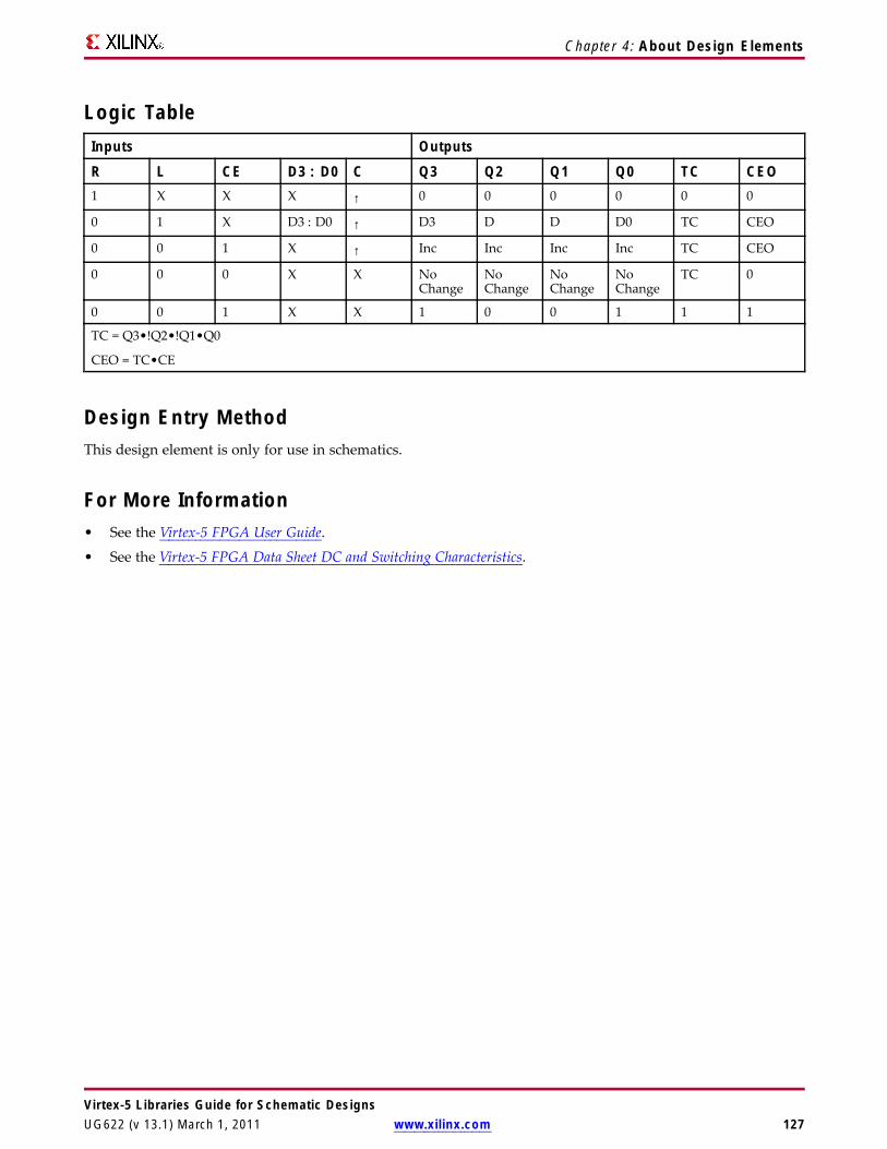
Chapter 4: About Design Elements
Logic TableInputs Outputs
R L CE D3 : D0 C Q3 Q2 Q1 Q0 TC CEO1 X X X ↑ 0 0 0 0 0 0
0 1 X D3 : D0 ↑ D3 D D D0 TC CEO
0 0 1 X ↑ Inc Inc Inc Inc TC CEO
0 0 0 X X NoChange
NoChange
NoChange
NoChange
TC 0
0 0 1 X X 1 0 0 1 1 1
TC = Q3•!Q2•!Q1•Q0
CEO = TC•CE
Design Entry MethodThis design element is only for use in schematics.
For More Information• See the Virtex-5 FPGA User Guide.
• See the Virtex-5 FPGA Data Sheet DC and Switching Characteristics.
Virtex-5 Libraries Guide for Schematic DesignsUG622 (v 13.1) March 1, 2011 www.xilinx.com 127

Chapter 4: About Design Elements
CFGLUT5Primitive: 5-input Dynamically Reconfigurable Look-Up Table (LUT)
IntroductionThis element is a runtime, dynamically reconfigurable, 5-input look-up table (LUT) that enables the changingof the logical function of the LUT during circuit operation. Using the CDI pin, a new INIT value can besynchronously shifted in serially to change the logical function. The O6 output pin produces the logical outputfunction, based on the current INIT value loaded into the LUT and the currently selected I0-I4 input pins.Optionally, you can use the O5 output in combination with the O6 output to create two individual 4-inputfunctions sharing the same inputs or a 5-input function and a 4-input function that uses a subset of the 5-inputlogic (see tables below). This component occupies one of the four 6-LUT components within a slice.
To cascade this element, connect the CDO pin from each element to the CDI input of the next element. This willallow a single serial chain of data (32-bits per LUT) to reconfigure multiple LUTs.
Port DescriptionsPort Direction Width FunctionO6 Output 1 5-LUT output
O5 Output 1 4-LUT output
I0, I1, I2, I3, I4 Input 1 LUT inputs
CDO Output 1 Reconfiguration data cascaded output (optionally connect to the CDI inputof a subsequent LUT)
CDI Input 1 Reconfiguration data serial input
CLK Input 1 Reconfiguration clock
CE Input 1 Active high reconfiguration clock enable
Design Entry MethodThis design element can be used in schematics.• Connect the CLK input to the clock source used to supply the reconfiguration data.• Connect the CDI input to the source of the reconfiguration data.• Connect the CE pin to the active high logic if you need to enable/disable LUT reconfiguration.• Connect the I4-I0 pins to the source inputs to the logic equation. The logic function is output on O6 and O5.• To cascade this element, connect the CDO pin from each element to the CDI input of the next element to
allow a single serial chain of data to reconfigure multiple LUTs.
The INIT attribute should be placed on this design element to specify the initial logical function of the LUT. Anew INIT can be loaded into the LUT any time during circuit operation by shifting in 32-bits per LUT in thechain, representing the new INIT value. Disregard the O6 and O5 output data until all 32-bits of new INIT datahas been clocked into the LUT. The logical function of the LUT changes as new INIT data is shifted into it. Datashould be shifted in MSB (INIT[31]) first and LSB (INIT[0]) last.
Virtex-5 Libraries Guide for Schematic Designs128 www.xilinx.com UG622 (v 13.1) March 1, 2011

Chapter 4: About Design Elements
In order to understand the O6 and O5 logical value based on the current INIT, see the table below:
I4 I3 I2 I1 I0 O6 Value O5 Value1 1 1 1 1 INIT[31] INIT[15]
1 1 1 1 0 INIT[30] INIT[14]. . . . . . . . .
1 0 0 0 1 INIT[17] INIT[1]
1 0 0 0 0 INIT[16] INIT[0]
0 1 1 1 1 INIT[15] INIT[15]
0 1 1 1 0 INIT[14] INIT[14]. . . . . . . . .
0 0 0 0 1 INIT[1] INIT[1]
0 0 0 0 0 INIT[0] INIT[0]
For instance, the INIT value of FFFF8000 would represent the following logical equations:
• O6 = I4 or (I3 and I2 and I1 and I0)
• O5 = I3 and I2 and I1 and I0
To use these elements as two, 4-input LUTs with the same inputs but different functions, tie the I4 signal to alogical one. The INIT[31:16] values apply to the logical values of the O6 output and INIT [15:0] apply to thelogical values of the O5 output.
Available AttributesAttribute Type Allowed Values Default DescriptionINIT Hexadecimal Any 32-bit Value All zeros Specifies the initial logical expression of
this element.
For More Information• See the Virtex-5 FPGA User Guide.
• See the Virtex-5 FPGA Data Sheet DC and Switching Characteristics.
Virtex-5 Libraries Guide for Schematic DesignsUG622 (v 13.1) March 1, 2011 www.xilinx.com 129

Chapter 4: About Design Elements
CJ4CEMacro: 4-Bit Johnson Counter with Clock Enable and Asynchronous Clear
IntroductionThis design element is a clearable Johnson/shift counter. The asynchronous clear (CLR) input, when High,overrides all other inputs and forces the data (Q) outputs to logic level zero, independent of clock (C) transitions.The counter increments (shifts Q0 to Q1, Q1 to Q2,and so forth) when the clock enable input (CE) is High duringthe Low-to-High clock transition. Clock transitions are ignored when (CE) is Low.
The Q3 output is inverted and fed back to input Q0 to provide continuous counting operation.
This counter is asynchronously cleared, outputs Low, when power is applied. For FPGA devices, power-onconditions are simulated when global set/reset (GSR) is active. GSR defaults to active-High but can be invertedby adding an inverter in front of the GSR input of the appropriate STARTUP_architecture symbol.
Logic TableInputs Outputs
CLR CE C Q0 Q1 through Q31 X X 0 0
0 0 X No change No change
0 1 ↑ !q3 q0 through q2
q = state of referenced output one setup time prior to active clock transition
Design Entry MethodThis design element is only for use in schematics.
For More Information• See the Virtex-5 FPGA User Guide.
• See the Virtex-5 FPGA Data Sheet DC and Switching Characteristics.
Virtex-5 Libraries Guide for Schematic Designs130 www.xilinx.com UG622 (v 13.1) March 1, 2011
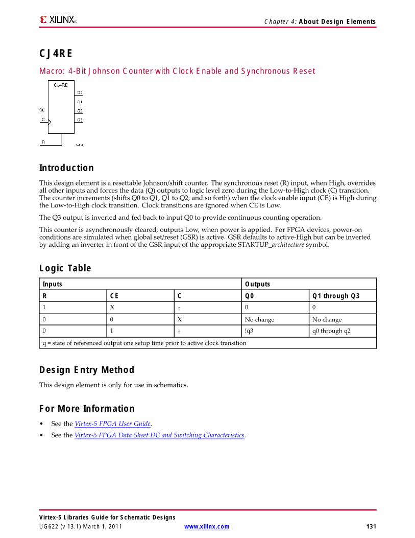
Chapter 4: About Design Elements
CJ4REMacro: 4-Bit Johnson Counter with Clock Enable and Synchronous Reset
IntroductionThis design element is a resettable Johnson/shift counter. The synchronous reset (R) input, when High, overridesall other inputs and forces the data (Q) outputs to logic level zero during the Low-to-High clock (C) transition.The counter increments (shifts Q0 to Q1, Q1 to Q2, and so forth) when the clock enable input (CE) is High duringthe Low-to-High clock transition. Clock transitions are ignored when CE is Low.
The Q3 output is inverted and fed back to input Q0 to provide continuous counting operation.
This counter is asynchronously cleared, outputs Low, when power is applied. For FPGA devices, power-onconditions are simulated when global set/reset (GSR) is active. GSR defaults to active-High but can be invertedby adding an inverter in front of the GSR input of the appropriate STARTUP_architecture symbol.
Logic TableInputs Outputs
R CE C Q0 Q1 through Q31 X ↑ 0 0
0 0 X No change No change
0 1 ↑ !q3 q0 through q2
q = state of referenced output one setup time prior to active clock transition
Design Entry MethodThis design element is only for use in schematics.
For More Information• See the Virtex-5 FPGA User Guide.
• See the Virtex-5 FPGA Data Sheet DC and Switching Characteristics.
Virtex-5 Libraries Guide for Schematic DesignsUG622 (v 13.1) March 1, 2011 www.xilinx.com 131
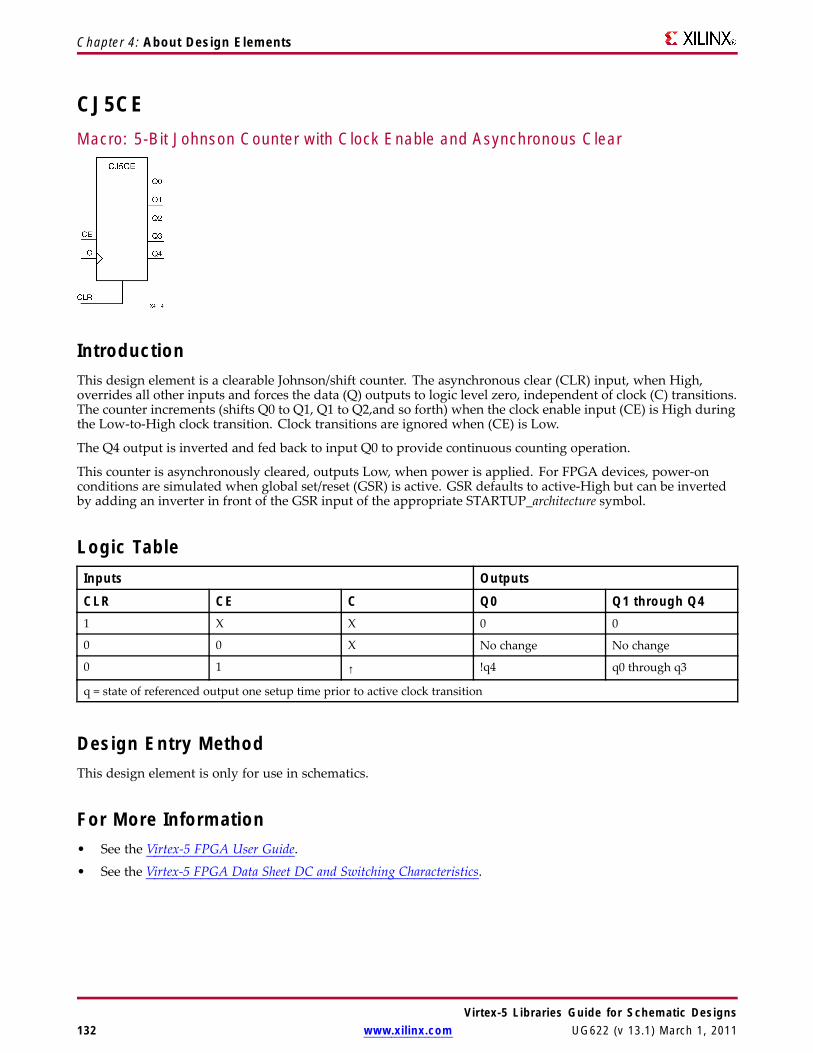
Chapter 4: About Design Elements
CJ5CEMacro: 5-Bit Johnson Counter with Clock Enable and Asynchronous Clear
IntroductionThis design element is a clearable Johnson/shift counter. The asynchronous clear (CLR) input, when High,overrides all other inputs and forces the data (Q) outputs to logic level zero, independent of clock (C) transitions.The counter increments (shifts Q0 to Q1, Q1 to Q2,and so forth) when the clock enable input (CE) is High duringthe Low-to-High clock transition. Clock transitions are ignored when (CE) is Low.
The Q4 output is inverted and fed back to input Q0 to provide continuous counting operation.
This counter is asynchronously cleared, outputs Low, when power is applied. For FPGA devices, power-onconditions are simulated when global set/reset (GSR) is active. GSR defaults to active-High but can be invertedby adding an inverter in front of the GSR input of the appropriate STARTUP_architecture symbol.
Logic TableInputs Outputs
CLR CE C Q0 Q1 through Q41 X X 0 0
0 0 X No change No change
0 1 ↑ !q4 q0 through q3
q = state of referenced output one setup time prior to active clock transition
Design Entry MethodThis design element is only for use in schematics.
For More Information• See the Virtex-5 FPGA User Guide.
• See the Virtex-5 FPGA Data Sheet DC and Switching Characteristics.
Virtex-5 Libraries Guide for Schematic Designs132 www.xilinx.com UG622 (v 13.1) March 1, 2011
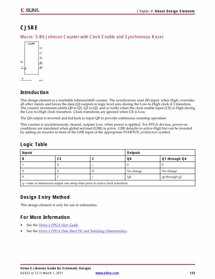
Chapter 4: About Design Elements
CJ5REMacro: 5-Bit Johnson Counter with Clock Enable and Synchronous Reset
IntroductionThis design element is a resettable Johnson/shift counter. The synchronous reset (R) input, when High, overridesall other inputs and forces the data (Q) outputs to logic level zero during the Low-to-High clock (C) transition.The counter increments (shifts Q0 to Q1, Q1 to Q2, and so forth) when the clock enable input (CE) is High duringthe Low-to-High clock transition. Clock transitions are ignored when CE is Low.
The Q4 output is inverted and fed back to input Q0 to provide continuous counting operation.
This counter is asynchronously cleared, outputs Low, when power is applied. For FPGA devices, power-onconditions are simulated when global set/reset (GSR) is active. GSR defaults to active-High but can be invertedby adding an inverter in front of the GSR input of the appropriate STARTUP_architecture symbol.
Logic TableInputs Outputs
R CE C Q0 Q1 through Q41 X ↑ 0 0
0 0 X No change No change
0 1 ↑ !q4 q0 through q3
q = state of referenced output one setup time prior to active clock transition
Design Entry MethodThis design element is only for use in schematics.
For More Information• See the Virtex-5 FPGA User Guide.
• See the Virtex-5 FPGA Data Sheet DC and Switching Characteristics.
Virtex-5 Libraries Guide for Schematic DesignsUG622 (v 13.1) March 1, 2011 www.xilinx.com 133
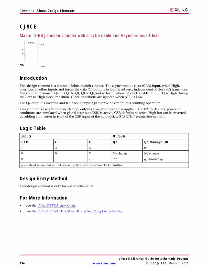
Chapter 4: About Design Elements
CJ8CEMacro: 8-Bit Johnson Counter with Clock Enable and Asynchronous Clear
IntroductionThis design element is a clearable Johnson/shift counter. The asynchronous clear (CLR) input, when High,overrides all other inputs and forces the data (Q) outputs to logic level zero, independent of clock (C) transitions.The counter increments (shifts Q0 to Q1, Q1 to Q2,and so forth) when the clock enable input (CE) is High duringthe Low-to-High clock transition. Clock transitions are ignored when (CE) is Low.
The Q7 output is inverted and fed back to input Q0 to provide continuous counting operation.
This counter is asynchronously cleared, outputs Low, when power is applied. For FPGA devices, power-onconditions are simulated when global set/reset (GSR) is active. GSR defaults to active-High but can be invertedby adding an inverter in front of the GSR input of the appropriate STARTUP_architecture symbol.
Logic TableInputs Outputs
CLR CE C Q0 Q1 through Q81 X X 0 0
0 0 X No change No change
0 1 ↑ !q7 q0 through q7
q = state of referenced output one setup time prior to active clock transition
Design Entry MethodThis design element is only for use in schematics.
For More Information• See the Virtex-5 FPGA User Guide.
• See the Virtex-5 FPGA Data Sheet DC and Switching Characteristics.
Virtex-5 Libraries Guide for Schematic Designs134 www.xilinx.com UG622 (v 13.1) March 1, 2011
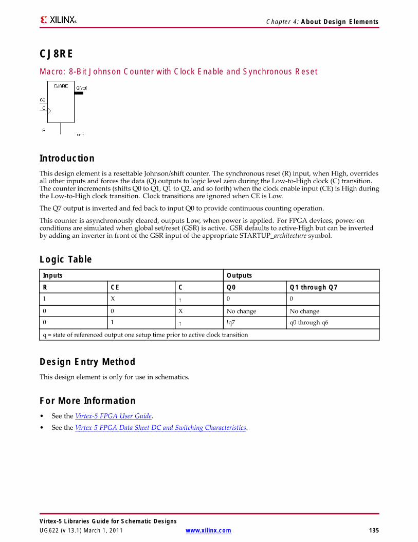
Chapter 4: About Design Elements
CJ8REMacro: 8-Bit Johnson Counter with Clock Enable and Synchronous Reset
IntroductionThis design element is a resettable Johnson/shift counter. The synchronous reset (R) input, when High, overridesall other inputs and forces the data (Q) outputs to logic level zero during the Low-to-High clock (C) transition.The counter increments (shifts Q0 to Q1, Q1 to Q2, and so forth) when the clock enable input (CE) is High duringthe Low-to-High clock transition. Clock transitions are ignored when CE is Low.
The Q7 output is inverted and fed back to input Q0 to provide continuous counting operation.
This counter is asynchronously cleared, outputs Low, when power is applied. For FPGA devices, power-onconditions are simulated when global set/reset (GSR) is active. GSR defaults to active-High but can be invertedby adding an inverter in front of the GSR input of the appropriate STARTUP_architecture symbol.
Logic TableInputs Outputs
R CE C Q0 Q1 through Q71 X ↑ 0 0
0 0 X No change No change
0 1 ↑ !q7 q0 through q6
q = state of referenced output one setup time prior to active clock transition
Design Entry MethodThis design element is only for use in schematics.
For More Information• See the Virtex-5 FPGA User Guide.
• See the Virtex-5 FPGA Data Sheet DC and Switching Characteristics.
Virtex-5 Libraries Guide for Schematic DesignsUG622 (v 13.1) March 1, 2011 www.xilinx.com 135

Chapter 4: About Design Elements
COMP16Macro: 16-Bit Identity Comparator
IntroductionThis design element is a 16-bit identity comparator. The equal output (EQ) is high when A15 : A0 and B15 :B0 are equal.
Equality is determined by a bit comparison of the two words. When any two of the corresponding bits fromeach word are not the same, the EQ output is Low.
Design Entry MethodThis design element is only for use in schematics.
For More Information• See the Virtex-5 FPGA User Guide.
• See the Virtex-5 FPGA Data Sheet DC and Switching Characteristics.
Virtex-5 Libraries Guide for Schematic Designs136 www.xilinx.com UG622 (v 13.1) March 1, 2011

Chapter 4: About Design Elements
COMP2Macro: 2-Bit Identity Comparator
IntroductionThis design element is a 2-bit identity comparator. The equal output (EQ) is High when the two words A1 : A0and B1 : B0 are equal.
Equality is determined by a bit comparison of the two words. When any two of the corresponding bits fromeach word are not the same, the EQ output is Low.
Design Entry MethodThis design element is only for use in schematics.
For More Information• See the Virtex-5 FPGA User Guide.
• See the Virtex-5 FPGA Data Sheet DC and Switching Characteristics.
Virtex-5 Libraries Guide for Schematic DesignsUG622 (v 13.1) March 1, 2011 www.xilinx.com 137

Chapter 4: About Design Elements
COMP4Macro: 4-Bit Identity Comparator
IntroductionThis design element is a 4-bit identity comparator. The equal output (EQ) is high when A3 : A0 and B3 : B0 areequal.
Equality is determined by a bit comparison of the two words. When any two of the corresponding bits fromeach word are not the same, the EQ output is Low.
Design Entry MethodThis design element is only for use in schematics.
For More Information• See the Virtex-5 FPGA User Guide.
• See the Virtex-5 FPGA Data Sheet DC and Switching Characteristics.
Virtex-5 Libraries Guide for Schematic Designs138 www.xilinx.com UG622 (v 13.1) March 1, 2011

Chapter 4: About Design Elements
COMP8Macro: 8-Bit Identity Comparator
IntroductionThis design element is an 8-bit identity comparator. The equal output (EQ) is high when A7 : A0 and B7 :B0 are equal.
Equality is determined by a bit comparison of the two words. When any two of the corresponding bits fromeach word are not the same, the EQ output is Low.
Design Entry MethodThis design element is only for use in schematics.
For More Information• See the Virtex-5 FPGA User Guide.
• See the Virtex-5 FPGA Data Sheet DC and Switching Characteristics.
Virtex-5 Libraries Guide for Schematic DesignsUG622 (v 13.1) March 1, 2011 www.xilinx.com 139

Chapter 4: About Design Elements
COMPM16Macro: 16-Bit Magnitude Comparator
IntroductionThis design element is a 16-bit magnitude comparator that compare two positive Binary-weighted words. Itcompares A15 : A0 and B15 : B0, where A15 and B15 are the most significant bits.
The greater-than output (GT) is High when A > B, and the less-than output (LT) is High when A < B Whenthe two words are equal, both GT and LT are Low. Equality can be measured with this macro by comparingboth outputs with a NOR gate.
Logic TableInputs Outputs
A7, B7 A6, B6 A5, B5 A4, B4 A3, B3 A2, B2 A1, B1 A0, B0 GT LTA7>B7 X X X X X X X 1 0
A7<B7 X X X X X X X 0 1
A7=B7 A6>B6 X X X X X X 1 0
A7=B7 A6<B6 X X X X X X 0 1
A7=B7 A6=B6 A5>B5 X X X X X 1 0
A7=B7 A6=B6 A5<B5 X X X X X 0 1
A7=B7 A6=B6 A5=B5 A4>B4 X X X X 1 0
A7=B7 A6=B6 A5=B5 A4<B4 X X X X 0 1
A7=B7 A6=B6 A5=B5 A4=B4 A3>B3 X X X 1 0
A7=B7 A6=B6 A5=B5 A4=B4 A3<B3 X X X 0 1
A7=B7 A6=B6 A5=B5 A4=B4 A3=B3 A2>B2 X X 1 0
A7=B7 A6=B6 A5=B5 A4=B4 A3=B3 A2<B2 X X 0 1
A7=B7 A6=B6 A5=B5 A4=B4 A3=B3 A2=B2 A1>B1 X 1 0
A7=B7 A6=B6 A5=B5 A4=B4 A3=B3 A2=B2 A1<B1 X 0 1
A7=B7 A6=B6 A5=B5 A4=B4 A3=B3 A2=B2 A1=B1 A0>B0 1 0
A7=B7 A6=B6 A5=B5 A4=B4 A3=B3 A2=B2 A1=B1 A0<B0 0 1
A7=B7 A6=B6 A5=B5 A4=B4 A3=B3 A2=B2 A1=B1 A0=B0 0 0
Design Entry MethodThis design element is only for use in schematics.
Virtex-5 Libraries Guide for Schematic Designs140 www.xilinx.com UG622 (v 13.1) March 1, 2011

Chapter 4: About Design Elements
For More Information• See the Virtex-5 FPGA User Guide.
• See the Virtex-5 FPGA Data Sheet DC and Switching Characteristics.
Virtex-5 Libraries Guide for Schematic DesignsUG622 (v 13.1) March 1, 2011 www.xilinx.com 141

Chapter 4: About Design Elements
COMPM2Macro: 2-Bit Magnitude Comparator
IntroductionThis design element is a 2-bit magnitude comparator that compare two positive binary-weighted words. Itcompares A1 : A0 and B1 : B0, where A1 and B1 are the most significant bits.
The greater-than output (GT) is High when A > B, and the less-than output (LT) is High when A < B Whenthe two words are equal, both GT and LT are Low. Equality can be measured with this macro by comparingboth outputs with a NOR gate.
Logic TableInputs Outputs
A1 B1 A0 B0 GT LT0 0 0 0 0 0
0 0 1 0 1 0
0 0 0 1 0 1
0 0 1 1 0 0
1 1 0 0 0 0
1 1 1 0 1 0
1 1 0 1 0 1
1 1 1 1 0 0
1 0 X X 1 0
0 1 X X 0 1
Design Entry MethodThis design element is only for use in schematics.
For More Information• See the Virtex-5 FPGA User Guide.
• See the Virtex-5 FPGA Data Sheet DC and Switching Characteristics.
Virtex-5 Libraries Guide for Schematic Designs142 www.xilinx.com UG622 (v 13.1) March 1, 2011
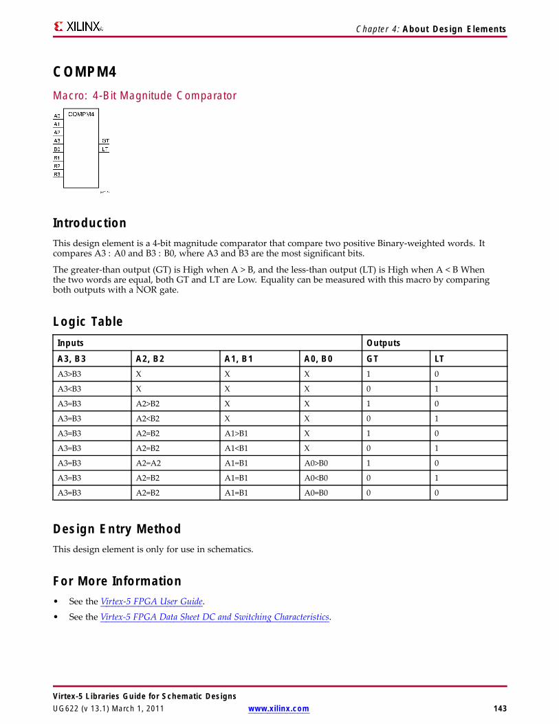
Chapter 4: About Design Elements
COMPM4Macro: 4-Bit Magnitude Comparator
IntroductionThis design element is a 4-bit magnitude comparator that compare two positive Binary-weighted words. Itcompares A3 : A0 and B3 : B0, where A3 and B3 are the most significant bits.
The greater-than output (GT) is High when A > B, and the less-than output (LT) is High when A < B Whenthe two words are equal, both GT and LT are Low. Equality can be measured with this macro by comparingboth outputs with a NOR gate.
Logic TableInputs Outputs
A3, B3 A2, B2 A1, B1 A0, B0 GT LTA3>B3 X X X 1 0
A3<B3 X X X 0 1
A3=B3 A2>B2 X X 1 0
A3=B3 A2<B2 X X 0 1
A3=B3 A2=B2 A1>B1 X 1 0
A3=B3 A2=B2 A1<B1 X 0 1
A3=B3 A2=A2 A1=B1 A0>B0 1 0
A3=B3 A2=B2 A1=B1 A0<B0 0 1
A3=B3 A2=B2 A1=B1 A0=B0 0 0
Design Entry MethodThis design element is only for use in schematics.
For More Information• See the Virtex-5 FPGA User Guide.
• See the Virtex-5 FPGA Data Sheet DC and Switching Characteristics.
Virtex-5 Libraries Guide for Schematic DesignsUG622 (v 13.1) March 1, 2011 www.xilinx.com 143
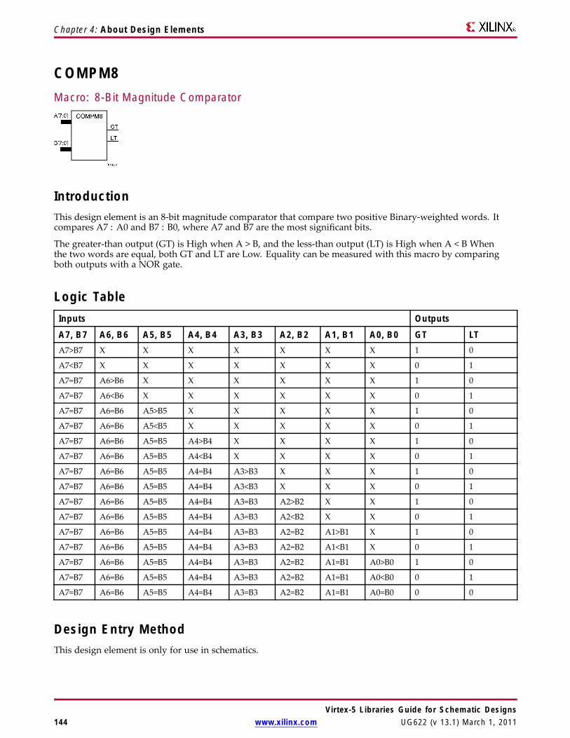
Chapter 4: About Design Elements
COMPM8Macro: 8-Bit Magnitude Comparator
IntroductionThis design element is an 8-bit magnitude comparator that compare two positive Binary-weighted words. Itcompares A7 : A0 and B7 : B0, where A7 and B7 are the most significant bits.
The greater-than output (GT) is High when A > B, and the less-than output (LT) is High when A < B Whenthe two words are equal, both GT and LT are Low. Equality can be measured with this macro by comparingboth outputs with a NOR gate.
Logic TableInputs Outputs
A7, B7 A6, B6 A5, B5 A4, B4 A3, B3 A2, B2 A1, B1 A0, B0 GT LTA7>B7 X X X X X X X 1 0
A7<B7 X X X X X X X 0 1
A7=B7 A6>B6 X X X X X X 1 0
A7=B7 A6<B6 X X X X X X 0 1
A7=B7 A6=B6 A5>B5 X X X X X 1 0
A7=B7 A6=B6 A5<B5 X X X X X 0 1
A7=B7 A6=B6 A5=B5 A4>B4 X X X X 1 0
A7=B7 A6=B6 A5=B5 A4<B4 X X X X 0 1
A7=B7 A6=B6 A5=B5 A4=B4 A3>B3 X X X 1 0
A7=B7 A6=B6 A5=B5 A4=B4 A3<B3 X X X 0 1
A7=B7 A6=B6 A5=B5 A4=B4 A3=B3 A2>B2 X X 1 0
A7=B7 A6=B6 A5=B5 A4=B4 A3=B3 A2<B2 X X 0 1
A7=B7 A6=B6 A5=B5 A4=B4 A3=B3 A2=B2 A1>B1 X 1 0
A7=B7 A6=B6 A5=B5 A4=B4 A3=B3 A2=B2 A1<B1 X 0 1
A7=B7 A6=B6 A5=B5 A4=B4 A3=B3 A2=B2 A1=B1 A0>B0 1 0
A7=B7 A6=B6 A5=B5 A4=B4 A3=B3 A2=B2 A1=B1 A0<B0 0 1
A7=B7 A6=B6 A5=B5 A4=B4 A3=B3 A2=B2 A1=B1 A0=B0 0 0
Design Entry MethodThis design element is only for use in schematics.
Virtex-5 Libraries Guide for Schematic Designs144 www.xilinx.com UG622 (v 13.1) March 1, 2011
Chapter 4: About Design Elements
For More Information• See the Virtex-5 FPGA User Guide.
• See the Virtex-5 FPGA Data Sheet DC and Switching Characteristics.
Virtex-5 Libraries Guide for Schematic DesignsUG622 (v 13.1) March 1, 2011 www.xilinx.com 145

Chapter 4: About Design Elements
COMPMC16Macro: 16-Bit Magnitude Comparator
IntroductionThis design element is a 16-bit, magnitude comparator that compares two positive Binary weighted words A15 :A0 and B15 : B0, where A15 and B15 are the most significant bits.
This comparator is implemented using carry logic with relative location constraints to ensure efficient logicplacement.
The greater-than output (GT) is High when A>B, and the less-than output (LT) is High when A<B. When thetwo words are equal, both GT and LT are Low. Equality can be flagged with this macro by connecting bothoutputs to a NOR gate.
Logic TableInputs Outputs
A7, B7 A6, B6 A5, B5 A4, B4 A3, B3 A2, B2 A1, B1 A0, B0 GT LTA7>B7 X X X X X X X 1 0
A7<B7 X X X X X X X 0 1
A7=B7 A6>B6 X X X X X X 1 0
A7=B7 A6<B6 X X X X X X 0 1
A7=B7 A6=B6 A5>B5 X X X X X 1 0
A7=B7 A6=B6 A5<B5 X X X X X 0 1
A7=B7 A6=B6 A5=B5 A4>B4 X X X X 1 0
A7=B7 A6=B6 A5=B5 A4<B4 X X X X 0 1
A7=B7 A6=B6 A5=B5 A4=B4 A3>B3 X X X 1 0
A7=B7 A6=B6 A5=B5 A4=B4 A3<B3 X X X 0 1
A7=B7 A6=B6 A5=B5 A4=B4 A3=B3 A2>B2 X X 1 0
A7=B7 A6=B6 A5=B5 A4=B4 A3=B3 A2<B2 X X 0 1
A7=B7 A6=B6 A5=B5 A4=B4 A3=B3 A2=B2 A1>B1 X 1 0
A7=B7 A6=B6 A5=B5 A4=B4 A3=B3 A2=B2 A1<B1 X 0 1
A7=B7 A6=B6 A5=B5 A4=B4 A3=B3 A2=B2 A1=B1 A0>B0 1 0
A7=B7 A6=B6 A5=B5 A4=B4 A3=B3 A2=B2 A1=B1 A0<B0 0 1
A7=B7 A6=B6 A5=B5 A4=B4 A3=B3 A2=B2 A1=B1 A0=B0 0 0
Design Entry MethodThis design element is only for use in schematics.
Virtex-5 Libraries Guide for Schematic Designs146 www.xilinx.com UG622 (v 13.1) March 1, 2011

Chapter 4: About Design Elements
For More Information• See the Virtex-5 FPGA User Guide.
• See the Virtex-5 FPGA Data Sheet DC and Switching Characteristics.
Virtex-5 Libraries Guide for Schematic DesignsUG622 (v 13.1) March 1, 2011 www.xilinx.com 147

Chapter 4: About Design Elements
COMPMC8Macro: 8-Bit Magnitude Comparator
IntroductionThis design element is an 8-bit, magnitude comparator that compares two positive Binaryweighted words A7 :A0 and B7 : B0, where A7 and B7 are the most significant bits.
This comparator is implemented using carry logic with relative location constraints to ensure efficient logicplacement.
The greater-than output (GT) is High when A>B, and the less-than output (LT) is High when A<B. When thetwo words are equal, both GT and LT are Low. Equality can be flagged with this macro by connecting bothoutputs to a NOR gate.
Logic TableInputs Outputs
A7, B7 A6, B6 A5, B5 A4, B4 A3, B3 A2, B2 A1, B1 A0, B0 GT LTA7>B7 X X X X X X X 1 0
A7<B7 X X X X X X X 0 1
A7=B7 A6>B6 X X X X X X 1 0
A7=B7 A6<B6 X X X X X X 0 1
A7=B7 A6=B6 A5>B5 X X X X X 1 0
A7=B7 A6=B6 A5<B5 X X X X X 0 1
A7=B7 A6=B6 A5=B5 A4>B4 X X X X 1 0
A7=B7 A6=B6 A5=B5 A4<B4 X X X X 0 1
A7=B7 A6=B6 A5=B5 A4=B4 A3>B3 X X X 1 0
A7=B7 A6=B6 A5=B5 A4=B4 A3<B3 X X X 0 1
A7=B7 A6=B6 A5=B5 A4=B4 A3=B3 A2>B2 X X 1 0
A7=B7 A6=B6 A5=B5 A4=B4 A3=B3 A2<B2 X X 0 1
A7=B7 A6=B6 A5=B5 A4=B4 A3=B3 A2=B2 A1>B1 X 1 0
A7=B7 A6=B6 A5=B5 A4=B4 A3=B3 A2=B2 A1<B1 X 0 1
A7=B7 A6=B6 A5=B5 A4=B4 A3=B3 A2=B2 A1=B1 A0>B0 1 0
A7=B7 A6=B6 A5=B5 A4=B4 A3=B3 A2=B2 A1=B1 A0<B0 0 1
A7=B7 A6=B6 A5=B5 A4=B4 A3=B3 A2=B2 A1=B1 A0=B0 0 0
Design Entry MethodThis design element is only for use in schematics.
Virtex-5 Libraries Guide for Schematic Designs148 www.xilinx.com UG622 (v 13.1) March 1, 2011

Chapter 4: About Design Elements
For More Information• See the Virtex-5 FPGA User Guide.
• See the Virtex-5 FPGA Data Sheet DC and Switching Characteristics.
Virtex-5 Libraries Guide for Schematic DesignsUG622 (v 13.1) March 1, 2011 www.xilinx.com 149
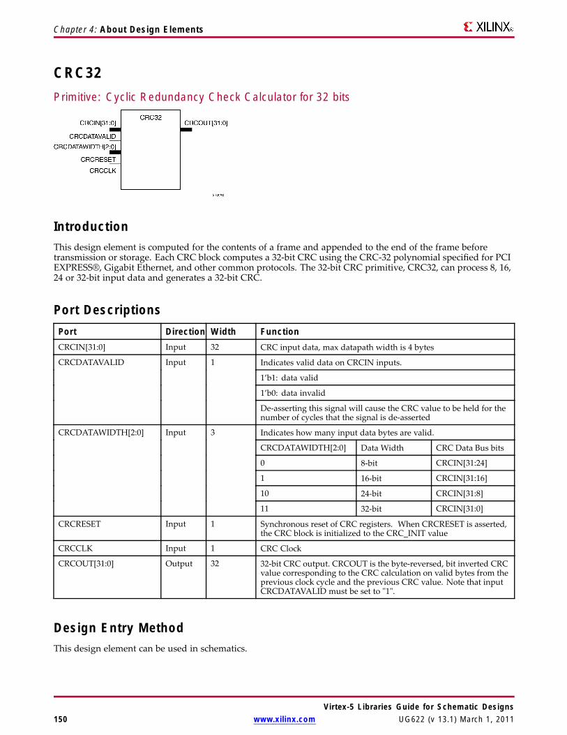
Chapter 4: About Design Elements
CRC32Primitive: Cyclic Redundancy Check Calculator for 32 bits
IntroductionThis design element is computed for the contents of a frame and appended to the end of the frame beforetransmission or storage. Each CRC block computes a 32-bit CRC using the CRC-32 polynomial specified for PCIEXPRESS®, Gigabit Ethernet, and other common protocols. The 32-bit CRC primitive, CRC32, can process 8, 16,24 or 32-bit input data and generates a 32-bit CRC.
Port DescriptionsPort Direction Width FunctionCRCIN[31:0] Input 32 CRC input data, max datapath width is 4 bytes
Indicates valid data on CRCIN inputs.
1’b1: data valid
1’b0: data invalid
CRCDATAVALID Input 1
De-asserting this signal will cause the CRC value to be held for thenumber of cycles that the signal is de-asserted
Indicates how many input data bytes are valid.
CRCDATAWIDTH[2:0] Data Width CRC Data Bus bits
0 8-bit CRCIN[31:24]
1 16-bit CRCIN[31:16]
10 24-bit CRCIN[31:8]
CRCDATAWIDTH[2:0] Input 3
11 32-bit CRCIN[31:0]
CRCRESET Input 1 Synchronous reset of CRC registers. When CRCRESET is asserted,the CRC block is initialized to the CRC_INIT value
CRCCLK Input 1 CRC Clock
CRCOUT[31:0] Output 32 32-bit CRC output. CRCOUT is the byte-reversed, bit inverted CRCvalue corresponding to the CRC calculation on valid bytes from theprevious clock cycle and the previous CRC value. Note that inputCRCDATAVALID must be set to "1".
Design Entry MethodThis design element can be used in schematics.
Virtex-5 Libraries Guide for Schematic Designs150 www.xilinx.com UG622 (v 13.1) March 1, 2011

Chapter 4: About Design Elements
Available Attributes
Attribute TypeAllowedvalues Default Description
CRC_INIT[31:0] Hexadecimal Any 32-BitValue
0xFFFFFFFF Sets the initial value of CRC internal registers.For LX30T & LX50T ES silicon the value is fixedas 0xFFFFFFFF.
For More Information• See the Virtex-5 FPGA User Guide.
• See the Virtex-5 FPGA Data Sheet DC and Switching Characteristics.
Virtex-5 Libraries Guide for Schematic DesignsUG622 (v 13.1) March 1, 2011 www.xilinx.com 151

Chapter 4: About Design Elements
CRC64Primitive: Cyclic Redundancy Check Calculator for 64 bits
IntroductionThis design element is computed for the contents of a frame, and appended to the end of the frame beforetransmission or storage. Each CRC block computes a 32-bit CRC using the CRC-32 polynomial specified for PCIEXPRESS®, Gigabit Ethernet, and other common protocols. The 64-bit CRC primitive, CRC64, can process 8,16, 24, 32, 40, 56 or 64-bit input data and generates a 32-bit CRC. Using the CRC64 primitive consumes bothCRC hard blocks paired with a given transceiver tile.
Port DescriptionsPort Direction Width FunctionCRCIN[63:0] Input 64 CRC input data, max datapath width is 8 bytes
Indicates valid data on CRCIN inputs.
1’b1: data valid
1’b0: data invalid
CRCDATAVALID Input 1
De-asserting this signal will cause the CRC value to be held for thenumber of cycles that the signal is de-asserted.
Indicates how many input data bytes are valid.
CRCDATAWIDTH [2:0] Data Width CRC Data Bus bits
0 8-bit CRCIN[63:56]
1 16-bit CRCIN[63:48]
10 24-bit CRCIN[63:40]
11 32-bit CRCIN[63:32]
100 40-bit CRCIN[63:24
101 48-bit CRCIN[63:16]
110 56-bit CRCIN[63:8]
CRCDATAWIDTH[2:0] Input 3
111 64-bit CRCIN[63:0]
CRCRESET Input 1 Synchronous reset of CRC registers. When CRCRESET is asserted,the CRC block is initialized to the CRC_INIT value.
CRCCLK Input 1 CRC Clock
CRCOUT[31:0] Output 32 32-bit CRC output. CRCOUT is the byte-reversed, bit inverted CRCvalue corresponding to the CRC calculation on valid bytes fromthe previous clock cycle and the previous CRC value. Note thatCRCDATAVALID must be set to "1".
Virtex-5 Libraries Guide for Schematic Designs152 www.xilinx.com UG622 (v 13.1) March 1, 2011
Chapter 4: About Design Elements
Design Entry MethodThis design element can be used in schematics.
Available Attributes
Attribute TypeAllowedvalues Default Description
CRC_INIT[31:0] Hexadecimal Any 32-BitValue
0xFFFFFFFF Sets the initial value of CRC internalregisters. For LX30T & LX50TES silicon the value is fixed as0xFFFFFFFF.
For More Information• See the Virtex-5 FPGA User Guide.
• See the Virtex-5 FPGA Data Sheet DC and Switching Characteristics.
Virtex-5 Libraries Guide for Schematic DesignsUG622 (v 13.1) March 1, 2011 www.xilinx.com 153
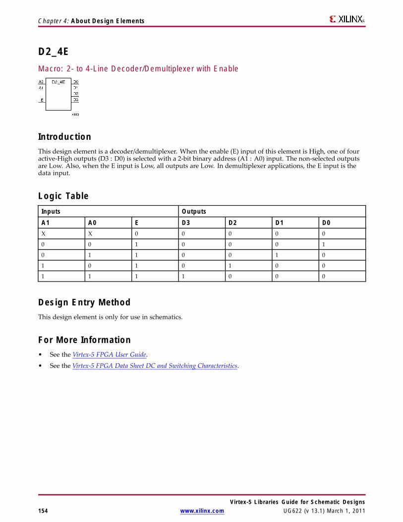
Chapter 4: About Design Elements
D2_4EMacro: 2- to 4-Line Decoder/Demultiplexer with Enable
IntroductionThis design element is a decoder/demultiplexer. When the enable (E) input of this element is High, one of fouractive-High outputs (D3 : D0) is selected with a 2-bit binary address (A1 : A0) input. The non-selected outputsare Low. Also, when the E input is Low, all outputs are Low. In demultiplexer applications, the E input is thedata input.
Logic TableInputs OutputsA1 A0 E D3 D2 D1 D0X X 0 0 0 0 0
0 0 1 0 0 0 1
0 1 1 0 0 1 0
1 0 1 0 1 0 0
1 1 1 1 0 0 0
Design Entry MethodThis design element is only for use in schematics.
For More Information• See the Virtex-5 FPGA User Guide.
• See the Virtex-5 FPGA Data Sheet DC and Switching Characteristics.
Virtex-5 Libraries Guide for Schematic Designs154 www.xilinx.com UG622 (v 13.1) March 1, 2011

Chapter 4: About Design Elements
D3_8EMacro: 3- to 8-Line Decoder/Demultiplexer with Enable
IntroductionWhen the enable (E) input of the D3_8E decoder/demultiplexer is High, one of eight active-High outputs (D7 :D0) is selected with a 3-bit binary address (A2 : A0) input. The non-selected outputs are Low. Also, when the Einput is Low, all outputs are Low. In demultiplexer applications, the E input is the data input.
Logic TableInputs OutputsA2 A1 A0 E D7 D6 D5 D4 D3 D2 D1 D0X X X 0 0 0 0 0 0 0 0 0
0 0 0 1 0 0 0 0 0 0 0 1
0 0 1 1 0 0 0 0 0 0 1 0
0 1 0 1 0 0 0 0 0 1 0 0
0 1 1 1 0 0 0 0 1 0 0 0
1 0 0 1 0 0 0 1 0 0 0 0
1 0 1 1 0 0 1 0 0 0 0 0
1 1 0 1 0 1 0 0 0 0 0 0
1 1 1 1 1 0 0 0 0 0 0 0
Design Entry MethodThis design element is only for use in schematics.
For More Information• See the Virtex-5 FPGA User Guide.
• See the Virtex-5 FPGA Data Sheet DC and Switching Characteristics.
Virtex-5 Libraries Guide for Schematic DesignsUG622 (v 13.1) March 1, 2011 www.xilinx.com 155
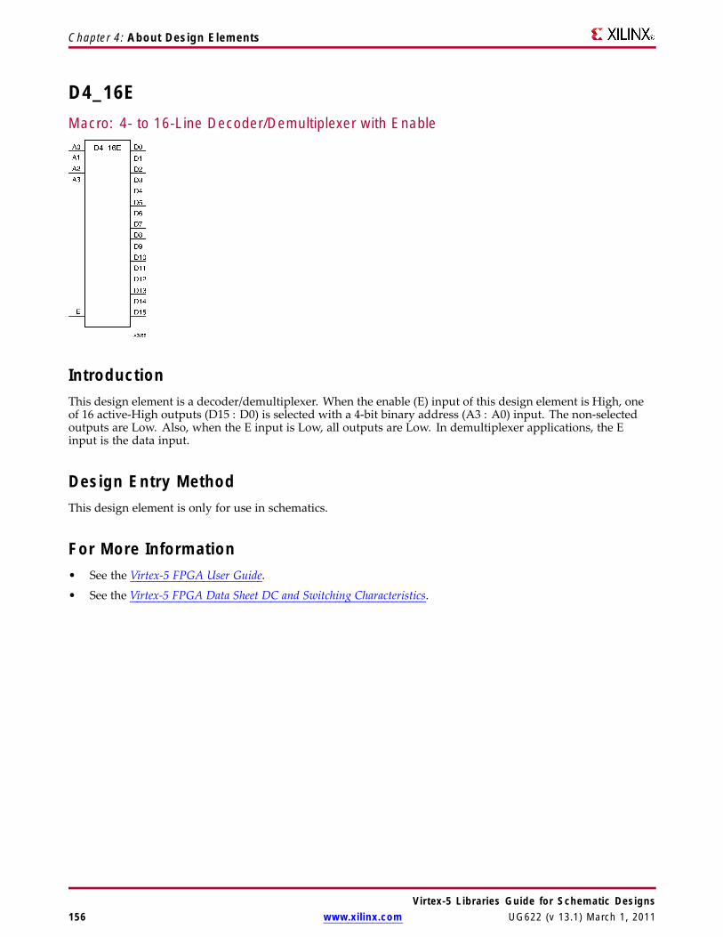
Chapter 4: About Design Elements
D4_16EMacro: 4- to 16-Line Decoder/Demultiplexer with Enable
IntroductionThis design element is a decoder/demultiplexer. When the enable (E) input of this design element is High, oneof 16 active-High outputs (D15 : D0) is selected with a 4-bit binary address (A3 : A0) input. The non-selectedoutputs are Low. Also, when the E input is Low, all outputs are Low. In demultiplexer applications, the Einput is the data input.
Design Entry MethodThis design element is only for use in schematics.
For More Information• See the Virtex-5 FPGA User Guide.
• See the Virtex-5 FPGA Data Sheet DC and Switching Characteristics.
Virtex-5 Libraries Guide for Schematic Designs156 www.xilinx.com UG622 (v 13.1) March 1, 2011

Chapter 4: About Design Elements
DCIRESETPrimitive: DCI State Machine Reset (After Configuration Has Been Completed)
IntroductionThis design element is used to reset the DCI state machine after configuration has been completed.
Port DescriptionsPort Type Width FunctionLOCKED Output 1 DCIRESET LOCK status output.
RST Input 1 DCIRESET asynchronous reset input.
Design Entry MethodThis design element can be used in schematics.
For More Information• See the Virtex-5 FPGA User Guide.
• See the Virtex-5 FPGA Data Sheet DC and Switching Characteristics.
Virtex-5 Libraries Guide for Schematic DesignsUG622 (v 13.1) March 1, 2011 www.xilinx.com 157

Chapter 4: About Design Elements
DCM_ADVPrimitive: Advanced Digital Clock Manager Circuit
IntroductionThis design element is a configurable/reconfigurable DLL with additional phase and frequency synthesis controlcapabilities. This component is commonly used for many FPGA applications in order to derive and control thevarious clocks needed within the system. If dynamic reconfiguration is not necessary, use either the DCM_BASEor DCM_PS components.
Port DescriptionsPort Direction Width FunctionClock Outputs/Inputs
CLK0 Output 1 The CLK0 output clock provides a clock with the same frequency as the DCM’seffective CLKIN frequency. By default, the effective CLKIN frequency is equal tothe CLKIN frequency, except when the CLKIN_DIVIDE_BY_2 attribute is set toTRUE. When CLKFB is connected, CLK0 is phase aligned to CLKIN.
CLK90 Output 1 The CLK90 output clock provides a clock with the same frequency as the DCM’sCLK0, only phase-shifted by 90°.
CLK180 Output 1 The CLK180 output clock provides a clock with the same frequency as the DCM’sCLK0, only phase-shifted by 180°.
CLK270 Output 1 The CLK270 output clock provides a clock with the same frequency as the DCM’sCLK0, only phase-shifted by 270°.
CLK2X Output 1 The CLK2X output clock provides a clock that is phase aligned to CLK0, withtwice the CLK0 frequency, and with an automatic 50/50 duty-cycle correction.Until the DCM is locked, the CLK2X output appears as a 1x version of the inputclock with a 25/75 duty cycle. This behavior allows the DCM to lock on the correctedge with respect to the source clock.
CLK2X180 Output 1 The CLK2X180 output clock provides a clock with the same frequency as theDCM’s CLK2X, only phase-shifted by 180°.
Virtex-5 Libraries Guide for Schematic Designs158 www.xilinx.com UG622 (v 13.1) March 1, 2011

Chapter 4: About Design Elements
Port Direction Width FunctionCLKDV Output 1 The frequency divide (CLKDV) output clock provides a clock that is phase aligned
to CLK0 with a frequency that is a fraction of the effective CLKIN frequency.The fraction is determined by the CLKDV_DIVIDE attribute. By default, theeffective CLKIN frequency is equal to the CLKIN frequency, except when theCLKIN_DIVIDE_BY_2 attribute is set to TRUE.
CLKFX Output 1 The frequency (CLKFX) output clock provides a clock with the followingfrequency definition:
CLKFX Frequency = (M/D) x (Effective CLKIN Frequency).
In this equation, M is the multiplier (numerator), with a value defined by theCLKFX_MULTIPLY attribute. D is the divisor (denominator), with a value definedby the CLKFX_DIVIDE attribute. Specifications for M and D, as well as input andoutput frequency ranges for the frequency synthesizer, are provided in the DataSheet for this architecture. The rising edge of CLKFX output is phase aligned tothe rising edges of CLK0, CLK2X, and CLKDV when the feedback path (CLKFB) isused. When M and D do have no common factor, the alignment occurs only onceevery D cycles of CLK0. By default, the effective CLKIN frequency is equal to theCLKIN frequency, except when the CLKIN_DIVIDE_BY_2 attribute is set to TRUE.
CLKFX180 Output 1 The CLKFX180 output clock provides a clock with the same frequency as theDCM’s CLKFX only phase-shifted by 180°.
CLKIN Input 1 The source clock (CLKIN) input pin provides the source clock to the DCM. TheCLKIN frequency must fall in the ranges specified in the Data Sheet for thisarchitecture. The clock input signal comes from one of the following buffers:
• IBUFG - Global Clock Input Buffer. The DCM compensates for the clock inputpath when an IBUFG, on the same edge (top or bottom) of the device, suchas the DCM, is used.
• BUFG/BUFGCTRL - Internal Global Clock Buffer. Any BUFGCTRL can driveany DCM in the device using the dedicated global routing. A BUFGCTRL candrive the DCM CLKIN pin when used to connect two DCM in series.
• IBUF - Input Buffer. When IBUF drives CLKIN input, the PAD to DCM inputskew is not compensated and increased jitter can occur. This configuration isgenerally not recommended.
CLKFB Input 1 The feedback clock (CLKFB) input pin provides a reference or feedback signal tothe DCM to delay-compensate the clock outputs and align it with the clock input.To provide the necessary feedback to the DCM, connect only the CLK0 output tothe CLKFB input via a BUFG component in the case of internal feedback or anOBUF ’ IBUFG to the case of external feedback. Set the CLK_FEEDBACK attributeto 1X. When the CLKFB pin is connected, CLK0, CLKDV, and CLKFX are phasealigned to CLKIN. When the CLKFB pin is not connected, set CLK_FEEDBACKto NONE and only the CLKFX and CLKFX180 outputs are valid, however, notphase aligned to CLKIN.
Status Outputs/Control Inputs
LOCKED Output 1 Synchronous output from the PLL that provides you with an indication that thePLL has achieved phase alignment and is ready for operation.
PSDONE Output 1 Dynamic CLKIN select input. When high, ’1’ CLKIN1 is selected and whilelow, ’0’ CLKIN2 is selected. If dual clock selection is not necessary, connect thisinput to a logic 1.
Virtex-5 Libraries Guide for Schematic DesignsUG622 (v 13.1) March 1, 2011 www.xilinx.com 159
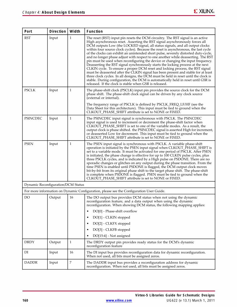
Chapter 4: About Design Elements
Port Direction Width FunctionRST Input 1 The reset (RST) input pin resets the DCM circuitry. The RST signal is an active
High asynchronous reset. Asserting the RST signal asynchronously forces allDCM outputs Low (the LOCKED signal, all status signals, and all output clockswithin four source clock cycles). Because the reset is asynchronous, the last cycleof the clocks can exhibit an unintended short pulse, severely distorted duty-cycle,and no longer phase adjust with respect to one another while deasserting. The RSTpin must be used when reconfiguring the device or changing the input frequency.Deasserting the RST signal synchronously starts the locking process at the nextCLKIN cycle. To ensure a proper DCM reset and locking process, the RST signalmust be deasserted after the CLKIN signal has been present and stable for at leastthree clock cycles. In all designs, the DCM must be held in reset until the clock isstable. During configuration, the DCM is automatically held in reset until GSR isreleased. If the clock is stable when GSR is released.
PSCLK Input 1 The phase-shift clock (PSCLK) input pin provides the source clock for the DCMphase shift. The phase-shift clock signal can be driven by any clock source(external or internal).
The frequency range of PSCLK is defined by PSCLK_FREQ_LF/HF (see theData Sheet for this architecture). This input must be tied to ground when theCLKOUT_PHASE_SHIFT attribute is set to NONE or FIXED.
PSINCDEC Input 1 The PSINCDEC input signal is synchronous with PSCLK. The PSINCDECinput signal is used to increment or decrement the phase-shift factor whenCLKOUT_PHASE_SHIFT is set to one of the variable modes. As a result, theoutput clock is phase shifted. the PSINCDEC signal is asserted High for increment,or deasserted Low for decrement. This input must be tied to ground when theCLKOUT_PHASE_SHIFT attribute is set to NONE or FIXED.
PSEN Input 1 The PSEN input signal is synchronous with PSCLK. A variable phase-shiftoperation is initiated by the PSEN input signal when CLKOUT_PHASE_SHIFT isset to a variable mode. It must be activated for one period of PSCLK. After PSENis initiated, the phase change is effective for up to 100 CLKIN pulse cycles, plusthree PSCLK cycles, and is indicated by a High pulse on PSDONE. There are nosporadic changes or glitches on any output during the phase transition. From thetime PSEN is enabled until PSDONE is flagged, the DCM output clock movesbit-by-bit from its original phase shift to the target phase shift. The phase-shiftis complete when PSDONE is flagged. PSEN must be tied to ground when theCLKOUT_PHASE_SHIFT attribute is set to NONE or FIXED.
Dynamic Reconfiguration/DCM Status
For more information on Dynamic Configuration, please see the Configuration User Guide.
DO Output 16 The DO output bus provides DCM status when not using the dynamicreconfiguration feature, and a data output when using the dynamicreconfiguration. When showing DCM status, the following mapping applies:
• DO[0] - Phase-shift overflow
• DO[1] - CLKIN stopped
• DO[2] - CLKFX stopped
• DO[3] - CLKFB stopped
• DO[15:4] - Not assigned
DRDY Output 1 The DRDY output pin provides ready status for the DCM’s dynamicreconfiguration feature
DI Input 16 The DI input bus provides reconfiguration data for dynamic reconfiguration.When not used, all bits must be assigned zeros.
DADDR Input 7 The DADDR input bus provides a reconfiguration address for dynamicreconfiguration. When not used, all bits must be assigned zeros.
Virtex-5 Libraries Guide for Schematic Designs160 www.xilinx.com UG622 (v 13.1) March 1, 2011

Chapter 4: About Design Elements
Port Direction Width FunctionDWE Input 1 The DWE input pin provides the write enable control signal to write the DI data
into the DADDR address. When not used, it must be tied Low.
DEN Input 1 The DEN input pin provides the enable control signal to access the dynamicreconfiguration feature. To reflect the DCM status signals on the DO output buswhen the dynamic reconfiguration feature is not used, DEN should be tied low.
DCLK Input 1 The DCLK input pin provides the source clock for the DCM’s dynamicreconfiguration circuit. The frequency of DCLK can be asynchronous (in phaseand frequency) to CLKIN. The dynamic reconfiguration clock signal is driven byany clock source. The frequency range of DCLK is described in the Data Sheet forthis architecture. When dynamic reconfiguration is not used, this input mustbe tied to ground.
Design Entry MethodThis design element can be used in schematics.
Available AttributesAttribute Type Allowed Values Default DescriptionCLK_FEEDBACK String "1X" , or "NONE" “1X” Specifies the clock feedback of the allowed
value.
CLKDV_DIVIDE Float 1.5, 2.0, 2.5, 3.0, 3.5,4.0, 4.5, 5.0, 5.5, 6.0,6.5, 7.0, 7.5, 8.0, 9.0,10.0, 11.0, 12.0, 13.0,14.0, 15.0, 16.0
2.0 Specifies the extent to which the CLKDLL,CLKDLLE, CLKDLLHF, or DCMclock divider (CLKDV output) is to befrequency divided.
CLKFX_DIVIDE Integer 1 to 32 1 Specifies the frequency divider value forthe CLKFX output.
CLKFX_MULTIPLY Integer 2 to 32 4 Specifies the frequency multiplier valuefor the CLKFX output.
CLKIN_DIVIDE_BY_2
Boolean FALSE, TRUE FALSE Allows for the input clock frequency to bedivided in half when such a reduction isnecessary to meet the DCM input clockfrequency requirements.
CLKIN_PERIOD Float 1.25 to 1000.00 10.0 Specifies period of input clock in ns from1.25 to 1000.00.
CLKOUT_PHASE_SHIFT
String "NONE","FIXED","VARIABLE_POSITIVE","VARIABLE_CENTER"or "DIRECT"
"NONE” Specifies the phase shift mode of allowedvalue.
DCM_PERFORMANCE_MODE
String "MAX_SPEED"or "MAX_RANGE”
"MAX_SPEED” Allows selection between maximumfrequency and minimum jitter for lowfrequency and maximum phase shiftrange.
Virtex-5 Libraries Guide for Schematic DesignsUG622 (v 13.1) March 1, 2011 www.xilinx.com 161

Chapter 4: About Design Elements
Attribute Type Allowed Values Default DescriptionDESKEW_ADJUST String "SOURCE_
SYNCHRONOUS","SYSTEM_SYNCHRONOUS"or "0" to "15”
"SYSTEM_SYNCHRONOUS"
Affects the amount of delay in thefeedback path, and should be used forsource-synchronous interfaces.
DFS_FREQUENCY_MODE
String "LOW" or "HIGH” "LOW” Specifies the frequency mode of thefrequency synthesizer.
DLL_FREQUENCY_MODE
String "LOW" or "HIGH” "LOW” Specifies the DLL’s frequency mode.
DUTY_CYCLE_CORRECTION
Boolean TRUE, FALSE TRUE Corrects the duty cycle of the CLK0,CLK90, CLK180, and CLK270 outputs.
FACTORY_JF Hexa-decimal
Any 16-Bit value. F0F0 The FACTORY_JF attribute affects theDCMs jitter filter characteristic. Thedefault value should not be modifiedunless otherwise instructed by Xilinx.
PHASE_SHIFT Integer -255 to 1023 0 Specifies the phase shiftnumerator. The range depends onCLKOUT_PHASE_SHIFT.
SIM_DEVICE String “VIRTEX4”or “VIRTEX5”
“VIRTEX5” Device selection.
STARTUP_WAIT Boolean FALSE, TRUE FALSE When TRUE, the configuration startupsequence waits in the specified cycle untilthe DCM locks.
For More Information• See the Virtex-5 FPGA User Guide.
• See the Virtex-5 FPGA Data Sheet DC and Switching Characteristics.
Virtex-5 Libraries Guide for Schematic Designs162 www.xilinx.com UG622 (v 13.1) March 1, 2011

Chapter 4: About Design Elements
DCM_BASEPrimitive: Base Digital Clock Manager Circuit
IntroductionThis design element is a configurable DLL with additional phase and frequency synthesis control capabilities.This component is commonly used for many FPGA applications in order to derive and control the various clocksneeded within the system. If dynamic reconfiguration is necessary, use the DCM_ADV component. If dynamicphase shift is required, use the DCM_PS component
Port DescriptionsPort Direction Width FunctionClock Outputs/Inputs
CLK0 Output 1 The CLK0 output clock provides a clock with the same frequency as the DCM’seffective CLKIN frequency. By default, the effective CLKIN frequency is equalto the CLKIN frequency, except when the CLKIN_DIVIDE_BY_2 attribute isset to TRUE. When CLKFB is connected, CLK0 is phase aligned to CLKIN.
CLK90 Output 1 The CLK90 output clock provides a clock with the same frequency as theDCM’s CLK0 only phase-shifted by 90°.
CLK180 Output 1 The CLK180 output clock provides a clock with the same frequency as theDCM’s CLK0 only phase-shifted by 180°.
CLK270 Output 1 The CLK270 output clock provides a clock with the same frequency as theDCM’s CLK0 only phase-shifted by 270°.
CLK2X Output 1 The CLK2X output clock provides a clock that is phase aligned to CLK0, withtwice the CLK0 frequency, and with an automatic 50/50 duty-cycle correction.Until the DCM is locked, the CLK2X output appears as a 1x version of theinput clock with a 25/75 duty cycle. This behavior allows the DCM to lock onthe correct edge with respect to the source clock.
CLK2X180 Output 1 The CLK2X180 output clock provides a clock with the same frequency as theDCM’s CLK2X only phase-shifted by 180°.
CLKDV Output 1 The frequency divide (CLKDV) output clock provides a clock that is phasealigned to CLK0 with a frequency that is a fraction of the effective CLKINfrequency. The fraction is determined by the CLKDV_DIVIDE attribute. Bydefault, the effective CLKIN frequency is equal to the CLKIN frequency, exceptwhen the CLKIN_DIVIDE_BY_2 attribute is set to TRUE.
Virtex-5 Libraries Guide for Schematic DesignsUG622 (v 13.1) March 1, 2011 www.xilinx.com 163

Chapter 4: About Design Elements
Port Direction Width FunctionCLKFX Output 1 The frequency (CLKFX) output clock provides a clock with the following
frequency definition:
CLKFX Frequency = (M/D) x (Effective CLKIN Frequency)
In this equation, M is the multiplier (numerator) with a value defined by theCLKFX_MULTIPLY attribute. D is the divisor (denominator) with a valuedefined by the CLKFX_DIVIDE attribute. Specifications for M and D, as wellas input and output frequency ranges for the frequency synthesizer, areprovided in the Data Sheet for this architecture. The rising edge of CLKFXoutput is phase aligned to the rising edges of CLK0, CLK2X, and CLKDVwhen the feedback path (CLKFB) is used. When M and D to have no commonfactor, the alignment occurs only once every D cycles of CLK0. By default, theeffective CLKIN frequency is equal to the CLKIN frequency, except when theCLKIN_DIVIDE_BY_2 attribute is set to TRUE.
CLKFX180 Output 1 The CLKFX180 output clock provides a clock with the same frequency as theDCM’s CLKFX only phase-shifted by 180°.
CLKIN Input 1 The source clock (CLKIN) input pin provides the source clock to the DCM. TheCLKIN frequency must fall in the ranges specified in the Data Sheet for thisarchitecture. The clock input signal comes from one of the following buffers:
• IBUFG - Global Clock Input Buffer. The DCM compensates for the clockinput path when an IBUFG on the same edge (top or bottom) of the deviceas the DCM is used.
• BUFG/BUFGCTRL - Internal Global Clock Buffer. Any BUFGCTRL candrive any DCM in the device using the dedicated global routing. ABUFGCTRL can drive the DCM CLKIN pin when used to connect twoDCM in series.
• IBUF - Input Buffer. When IBUF drives CLKIN input, the PAD to DCMinput skew is not compensated and increased jitter can occur. Thisconfiguration is generally not recommended.
CLKFB Input 1 The feedback clock (CLKFB) input pin provides a reference or feedback signalto the DCM to delay-compensate the clock outputs, and align it with theclock input. To provide the necessary feedback to the DCM, connect onlythe CLK0 output to the CLKFB input via a BUFG component in the case ofinternal feedback or an OBUF ’ IBUFG to the case of external feedback. Setthe CLK_FEEDBACK attribute to 1X. When the CLKFB pin is connected,CLK0, CLKDV, and CLKFX are phase aligned to CLKIN. When the CLKFB pinis not connected, set CLK_FEEDBACK to NONE and only the CLKFX andCLKFX180 outputs are valid. However, they are not phase aligned to CLKIN.
Status Outputs/Control Inputs
LOCKED Output 1 Synchronous output from the PLL that provides you with an indication thePLL has achieved phase alignment and is ready for operation.
RST Input 1 The reset (RST) input pin resets the DCM circuitry. The RST signal is an activeHigh asynchronous reset. Asserting the RST signal asynchronously forcesall DCM outputs Low (the LOCKED signal, all status signals, and all outputclocks within four source clock cycles). Because the reset is asynchronous,the last cycle of the clocks can exhibit an unintended short pulse, severelydistorted duty-cycle, and no longer phase adjust with respect to one anotherwhile deasserting. The RST pin must be used when reconfiguring the deviceor changing the input frequency. Deasserting the RST signal synchronouslystarts the locking process at the next CLKIN cycle. To ensure a proper DCMreset and locking process, the RST signal must be deasserted after the CLKINsignal has been present and stable for at least three clock cycles. In all designs,the DCM must be held in reset until the clock is stable. During configuration,the DCM is automatically held in reset until GSR is released. If the clock isstable when GSR is released.
Virtex-5 Libraries Guide for Schematic Designs164 www.xilinx.com UG622 (v 13.1) March 1, 2011
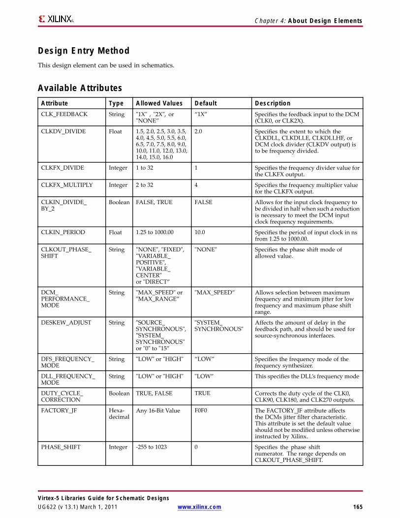
Chapter 4: About Design Elements
Design Entry MethodThis design element can be used in schematics.
Available AttributesAttribute Type Allowed Values Default DescriptionCLK_FEEDBACK String "1X" , "2X", or
"NONE”“1X” Specifies the feedback input to the DCM
(CLK0, or CLK2X).
CLKDV_DIVIDE Float 1.5, 2.0, 2.5, 3.0, 3.5,4.0, 4.5, 5.0, 5.5, 6.0,6.5, 7.0, 7.5, 8.0, 9.0,10.0, 11.0, 12.0, 13.0,14.0, 15.0, 16.0
2.0 Specifies the extent to which theCLKDLL, CLKDLLE, CLKDLLHF, orDCM clock divider (CLKDV output) isto be frequency divided.
CLKFX_DIVIDE Integer 1 to 32 1 Specifies the frequency divider value forthe CLKFX output.
CLKFX_MULTIPLY Integer 2 to 32 4 Specifies the frequency multiplier valuefor the CLKFX output.
CLKIN_DIVIDE_BY_2
Boolean FALSE, TRUE FALSE Allows for the input clock frequency tobe divided in half when such a reductionis necessary to meet the DCM inputclock frequency requirements.
CLKIN_PERIOD Float 1.25 to 1000.00 10.0 Specifies the period of input clock in nsfrom 1.25 to 1000.00.
CLKOUT_PHASE_SHIFT
String "NONE", "FIXED","VARIABLE_POSITIVE","VARIABLE_CENTER"or "DIRECT”
"NONE" Specifies the phase shift mode ofallowed value.
DCM_PERFORMANCE_MODE
String "MAX_SPEED" or"MAX_RANGE”
"MAX_SPEED” Allows selection between maximumfrequency and minimum jitter for lowfrequency and maximum phase shiftrange.
DESKEW_ADJUST String "SOURCE_SYNCHRONOUS","SYSTEM_SYNCHRONOUS"or "0" to "15”
"SYSTEM_SYNCHRONOUS"
Affects the amount of delay in thefeedback path, and should be used forsource-synchronous interfaces.
DFS_FREQUENCY_MODE
String "LOW" or "HIGH" “LOW” Specifies the frequency mode of thefrequency synthesizer.
DLL_FREQUENCY_MODE
String "LOW" or "HIGH" "LOW” This specifies the DLL’s frequency mode
DUTY_CYCLE_CORRECTION
Boolean TRUE, FALSE TRUE Corrects the duty cycle of the CLK0,CLK90, CLK180, and CLK270 outputs.
FACTORY_JF Hexa-decimal
Any 16-Bit Value F0F0 The FACTORY_JF attribute affectsthe DCMs jitter filter characteristic.This attribute is set the default valueshould not be modified unless otherwiseinstructed by Xilinx.
PHASE_SHIFT Integer -255 to 1023 0 Specifies the phase shiftnumerator. The range depends onCLKOUT_PHASE_SHIFT.
Virtex-5 Libraries Guide for Schematic DesignsUG622 (v 13.1) March 1, 2011 www.xilinx.com 165

Chapter 4: About Design Elements
Attribute Type Allowed Values Default DescriptionSTARTUP_WAIT Boolean FALSE, TRUE FALSE When set to TRUE, the configuration
startup sequence waits in the specifiedcycle until the DCM locks.
For More Information• See the Virtex-5 FPGA User Guide.
• See the Virtex-5 FPGA Data Sheet DC and Switching Characteristics.
Virtex-5 Libraries Guide for Schematic Designs166 www.xilinx.com UG622 (v 13.1) March 1, 2011

Chapter 4: About Design Elements
DCM_PSPrimitive: Digital Clock Manager with Basic and Phase Shift Features
IntroductionThis design element is a configurable DLL with additional phase and frequency synthesis control capabilities.This component is commonly used for many FPGA applications in order to derive and control the various clocksneeded within the system. If dynamic reconfiguration is necessary, use the DCM_ADV. If Dynamic Phaseshift is not necessary, use the DCM_BASE component.
Port DescriptionsPort Direction Width FunctionClock Outputs/Inputs
CLK0 Output 1 The CLK0 output clock provides a clock with the same frequencyas the DCM’s effective CLKIN frequency. By default, the effectiveCLKIN frequency is equal to the CLKIN frequency, except whenthe CLKIN_DIVIDE_BY_2 attribute is set to TRUE. When CLKFB isconnected, CLK0 is phase aligned to CLKIN.
CLK90 Output 1 The CLK90 output clock provides a clock with the same frequency as theDCM’s CLK0 only phase-shifted by 90°.
CLK180 Output 1 The CLK180 output clock provides a clock with the same frequency as theDCM’s CLK0 only phase-shifted by 180°.
CLK270 Output 1 The CLK270 output clock provides a clock with the same frequency as theDCM’s CLK0 only phase-shifted by 270°.
CLK2X Output 1 The CLK2X output clock provides a clock that is phase aligned to CLK0,with twice the CLK0 frequency, and with an automatic 50/50 duty-cyclecorrection. Until the DCM is locked, the CLK2X output appears as a 1xversion of the input clock with a 25/75 duty cycle. This behavior allowsthe DCM to lock on the correct edge with respect to the source clock.
CLK2X180 Output 1 The CLK2X180 output clock provides a clock with the same frequency asthe DCM’s CLK2X only phase-shifted by 180°.
Virtex-5 Libraries Guide for Schematic DesignsUG622 (v 13.1) March 1, 2011 www.xilinx.com 167

Chapter 4: About Design Elements
Port Direction Width FunctionCLKDV Output 1 The frequency divide (CLKDV) output clock provides a clock that is
phase aligned to CLK0 with a frequency that is a fraction of the effectiveCLKIN frequency. The fraction is determined by the CLKDV_DIVIDEattribute. By default, the effective CLKIN frequency is equal to the CLKINfrequency, except when the CLKIN_DIVIDE_BY_2 attribute is set to TRUE.
CLKFX Output 1 The frequency (CLKFX) output clock provides a clock with the followingfrequency definition:
CLKFX Frequency = (M/D) x (Effective CLKIN Frequency)
In this equation, M is the multiplier (numerator) with a value defined bythe CLKFX_MULTIPLY attribute. D is the divisor (denominator) witha value defined by the CLKFX_DIVIDE attribute. Specifications for Mand D, as well as input and output frequency ranges for the frequencysynthesizer, are provided in the Data Sheet. The rising edge of CLKFXoutput is phase aligned to the rising edges of CLK0, CLK2X, and CLKDVwhen the feedback path (CLKFB) is used. When M and D to have nocommon factor, the alignment occurs only once every D cycles of CLK0. Bydefault, the effective CLKIN frequency is equal to the CLKIN frequency,except when the CLKIN_DIVIDE_BY_2 attribute is set to TRUE.
CLKFX180 Output 1 The CLKFX180 output clock provides a clock with the same frequency asthe DCM’s CLKFX only phase-shifted by 180°.
CLKIN Input 1 The source clock (CLKIN) input pin provides the source clock to the DCM.The CLKIN frequency must fall in the ranges specified in the Data Sheet.The clock input signal comes from one of the following buffers:
• IBUFG - Global Clock Input Buffer. The DCM compensates for theclock input path when an IBUFG on the same edge (top or bottom) ofthe device as the DCM is used.
• BUFG/BUFGCTRL - Internal Global Clock Buffer. Any BUFGCTRLcan drive any DCM in the device using the dedicated global routing.A BUFGCTRL can drive the DCM CLKIN pin when used to connecttwo DCM in series.
• IBUF - Input Buffer. When IBUF drives CLKIN input, the PAD toDCM input skew is not compensated and increased jitter can occur.This configuration is generally not recommended.
CLKFB Input 1 The feedback clock (CLKFB) input pin provides a reference or feedbacksignal to the DCM to delay-compensate the clock outputs, and align itwith the clock input. To provide the necessary feedback to the DCM,connect only the CLK0 output to the CLKFB input via a BUFG componentin the case of internal feedback or an OBUF ’ IBUFG to the case of externalfeedback. Set the CLK_FEEDBACK attribute to 1X. When the CLKFB pinis connected, CLK0, CLKDV, and CLKFX are phase aligned to CLKIN.When the CLKFB pin is not connected, set CLK_FEEDBACK to NONEand only the CLKFX and CLKFX180 outputs are valid. However, theyare not phase aligned to CLKIN.
Status Outputs/Control Inputs
LOCKED Output 1 Synchronous output from the PLL that provides you with an indicationthe PLL has achieved phase alignment and is ready for operation.
PSDONE Output 1 Dynamic CLKIN select input. When high, ’1’ CLKIN1 is selected andwhile low, ’0’ CLKIN2 is selected. If dual clock selection is not necessary,connect this input to a logic 1.
Virtex-5 Libraries Guide for Schematic Designs168 www.xilinx.com UG622 (v 13.1) March 1, 2011

Chapter 4: About Design Elements
Port Direction Width FunctionRST Input 1 The reset (RST) input pin resets the DCM circuitry. The RST signal is an
active High asynchronous reset. Asserting the RST signal asynchronouslyforces all DCM outputs Low (the LOCKED signal, all status signals, andall output clocks within four source clock cycles). Because the reset isasynchronous, the last cycle of the clocks can exhibit an unintended shortpulse, severely distorted duty-cycle, and no longer phase adjust withrespect to one another while deasserting. The RST pin must be used whenreconfiguring the device or changing the input frequency. Deasserting theRST signal synchronously starts the locking process at the next CLKINcycle. To ensure a proper DCM reset and locking process, the RST signalmust be deasserted after the CLKIN signal has been present and stable forat least three clock cycles. In all designs, the DCM must be held in resetuntil the clock is stable. During configuration, the DCM is automaticallyheld in reset until GSR is released. If the clock is stable when GSR is releas
PSCLK Input 1 The phase-shift clock (PSCLK) input pin provides the source clock forthe DCM phase shift. The phase-shift clock signal can be driven by anyclock source (external or internal).
The frequency range of PSCLK is defined by PSCLK_FREQ_LF/HF(see the Data Sheet). This input must be tied to ground when theCLKOUT_PHASE_SHIFT attribute is set to NONE or FIXED.
PSINCDEC Input 1 The PSINCDEC input signal is synchronous with PSCLK. The PSINCDECinput signal is used to increment or decrement the phase-shift factorwhen CLKOUT_PHASE_SHIFT is set to one of the variable modes. As aresult, the output clock is phase shifted. the PSINCDEC signal is assertedHigh for increment, or deasserted Low for decrement. This input mustbe tied to ground when the CLKOUT_PHASE_SHIFT attribute is set toNONE or FIXED.
PSEN Input 1 The PSEN input signal is synchronous with PSCLK. A variablephase-shift operation is initiated by the PSEN input signal whenCLKOUT_PHASE_SHIFT is set to a variable mode. It must be activatedfor one period of PSCLK. After PSEN is initiated, the phase change iseffective for up to 100 CLKIN pulse cycles, plus three PSCLK cycles, and isindicated by a High pulse on PSDONE. There are no sporadic changes orglitches on any output during the phase transition. From the time PSEN isenabled until PSDONE is flagged, the DCM output clock moves bit-by-bitfrom its original phase shift to the target phase shift. The phase-shift iscomplete when PSDONE is flagged. PSEN must be tied to ground whenthe CLKOUT_PHASE_SHIFT attribute is set to NONE or FIXED.
Design Entry MethodThis design element can be used in schematics.
Available AttributesAttribute Type Allowed Values Default DescriptionCLK_FEEDBACK String "1X", "2X",
or "NONE”"1X” Specifies the clock feedback of allowed
value.
CLKDV_DIVIDE FLOAT 1.5, 2.0, 2.5, 3.0, 3.5,4.0, 4.5, 5.0, 5.5, 6.0,6.5, 7.0, 7.5, 8.0, 9.0,10.0, 11.0, 12.0, 13.0,14.0, 15.0, 16.0
2.0 Specifies the extent to which the CLKDLL,CLKDLLE, CLKDLLHF, or DCM clockdivider (CLKDV output) is to be frequencydivided.
CLKFX_DIVIDE Integer 1 to 32 1 Specifies the frequency divider value for theCLKFX output.
Virtex-5 Libraries Guide for Schematic DesignsUG622 (v 13.1) March 1, 2011 www.xilinx.com 169
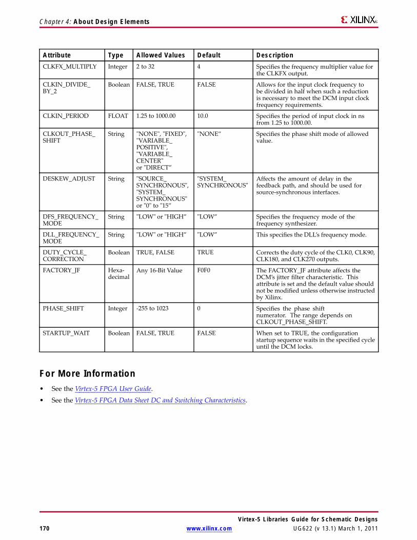
Chapter 4: About Design Elements
Attribute Type Allowed Values Default DescriptionCLKFX_MULTIPLY Integer 2 to 32 4 Specifies the frequency multiplier value for
the CLKFX output.
CLKIN_DIVIDE_BY_2
Boolean FALSE, TRUE FALSE Allows for the input clock frequency tobe divided in half when such a reductionis necessary to meet the DCM input clockfrequency requirements.
CLKIN_PERIOD FLOAT 1.25 to 1000.00 10.0 Specifies the period of input clock in nsfrom 1.25 to 1000.00.
CLKOUT_PHASE_SHIFT
String "NONE", "FIXED","VARIABLE_POSITIVE","VARIABLE_CENTER"or "DIRECT”
"NONE” Specifies the phase shift mode of allowedvalue.
DESKEW_ADJUST String "SOURCE_SYNCHRONOUS","SYSTEM_SYNCHRONOUS"or "0" to "15”
"SYSTEM_SYNCHRONOUS"
Affects the amount of delay in thefeedback path, and should be used forsource-synchronous interfaces.
DFS_FREQUENCY_MODE
String "LOW" or "HIGH” "LOW” Specifies the frequency mode of thefrequency synthesizer.
DLL_FREQUENCY_MODE
String "LOW" or "HIGH” "LOW” This specifies the DLL’s frequency mode.
DUTY_CYCLE_CORRECTION
Boolean TRUE, FALSE TRUE Corrects the duty cycle of the CLK0, CLK90,CLK180, and CLK270 outputs.
FACTORY_JF Hexa-decimal
Any 16-Bit Value F0F0 The FACTORY_JF attribute affects theDCM’s jitter filter characteristic. Thisattribute is set and the default value shouldnot be modified unless otherwise instructedby Xilinx.
PHASE_SHIFT Integer -255 to 1023 0 Specifies the phase shiftnumerator. The range depends onCLKOUT_PHASE_SHIFT.
STARTUP_WAIT Boolean FALSE, TRUE FALSE When set to TRUE, the configurationstartup sequence waits in the specified cycleuntil the DCM locks.
For More Information• See the Virtex-5 FPGA User Guide.
• See the Virtex-5 FPGA Data Sheet DC and Switching Characteristics.
Virtex-5 Libraries Guide for Schematic Designs170 www.xilinx.com UG622 (v 13.1) March 1, 2011

Chapter 4: About Design Elements
DEC_CC16Macro: 16-Bit Active Low Decoder
IntroductionThis design element is a 16-bit decoder that is used to build wide-decoder functions. It is implemented bycascading CY_MUX elements driven by look-up tables (LUTs). The C_IN pin can only be driven by the output (O)of a previous decode stage. When one or more of the inputs (A) are Low, the output is Low. When all the inputsare High and the C_IN input is High, the output is High. You can decode patterns by adding inverters to inputs.
Logic TableInputs Outputs
A0 A1 … Az C_IN O1 1 1 1 1 1
X X X X 0 0
0 X X X X 0
X 0 X X X 0
X X X 0 X 0
z = 3 for DEC_CC4; z = 7 for DEC_CC8; z = 15 for DEC_CC16
Design Entry MethodThis design element is only for use in schematics.
Virtex-5 Libraries Guide for Schematic DesignsUG622 (v 13.1) March 1, 2011 www.xilinx.com 171

Chapter 4: About Design Elements
For More Information• See the Virtex-5 FPGA User Guide.
• See the Virtex-5 FPGA Data Sheet DC and Switching Characteristics.
Virtex-5 Libraries Guide for Schematic Designs172 www.xilinx.com UG622 (v 13.1) March 1, 2011

Chapter 4: About Design Elements
DEC_CC4Macro: 4-Bit Active Low Decoder
IntroductionThis design element is a 4-bit decoder that is used to build wide-decoder functions. It is implemented bycascading CY_MUX elements driven by look-up tables (LUTs). The C_IN pin can only be driven by the output (O)of a previous decode stage. When one or more of the inputs (A) are Low, the output is Low. When all the inputsare High and the C_IN input is High, the output is High. You can decode patterns by adding inverters to inputs.
Logic TableInputs Outputs
A0 A1 … Az C_IN O1 1 1 1 1 1
X X X X 0 0
0 X X X X 0
X 0 X X X 0
X X X 0 X 0
z = 3 for DEC_CC4; z = 7 for DEC_CC8; z = 15 for DEC_CC16
Design Entry MethodThis design element is only for use in schematics.
For More Information• See the Virtex-5 FPGA User Guide.
• See the Virtex-5 FPGA Data Sheet DC and Switching Characteristics.
Virtex-5 Libraries Guide for Schematic DesignsUG622 (v 13.1) March 1, 2011 www.xilinx.com 173

Chapter 4: About Design Elements
DEC_CC8Macro: 8-Bit Active Low Decoder
IntroductionThis design element is a 8-bit decoder that is used to build wide-decoder functions. It is implemented bycascading CY_MUX elements driven by look-up tables (LUTs). The C_IN pin can only be driven by the output (O)of a previous decode stage. When one or more of the inputs (A) are Low, the output is Low. When all the inputsare High and the C_IN input is High, the output is High. You can decode patterns by adding inverters to inputs.
Logic TableInputs Outputs
A0 A1 … Az C_IN O1 1 1 1 1 1
X X X X 0 0
0 X X X X 0
X 0 X X X 0
X X X 0 X 0
z = 3 for DEC_CC4; z = 7 for DEC_CC8; z = 15 for DEC_CC16
Design Entry MethodThis design element is only for use in schematics.
For More Information• See the Virtex-5 FPGA User Guide.
• See the Virtex-5 FPGA Data Sheet DC and Switching Characteristics.
Virtex-5 Libraries Guide for Schematic Designs174 www.xilinx.com UG622 (v 13.1) March 1, 2011

Chapter 4: About Design Elements
DSP48EPrimitive: 25x18 Two’s Complement Multiplier with Integrated 48-Bit, 3-InputAdder/Subtracter/Accumulator or 2-Input Logic Unit
IntroductionThis design element is a versatile, scalable, hard IP block that allows for the creation of compact, high-speed,arithmetic-intensive operations, such as those seen for many DSP algorithms. Some of the functions capablewithin the block include multiplication, addition, subtraction, accumulation, shifting, logical operations, andpattern detection.
Port DescriptionsPort Direction Width Function
Data Ports
A Input 30 25-bit data input to multiplier or 30-bit MSB Data input toAdder/Logic Unit (LU).
Virtex-5 Libraries Guide for Schematic DesignsUG622 (v 13.1) March 1, 2011 www.xilinx.com 175
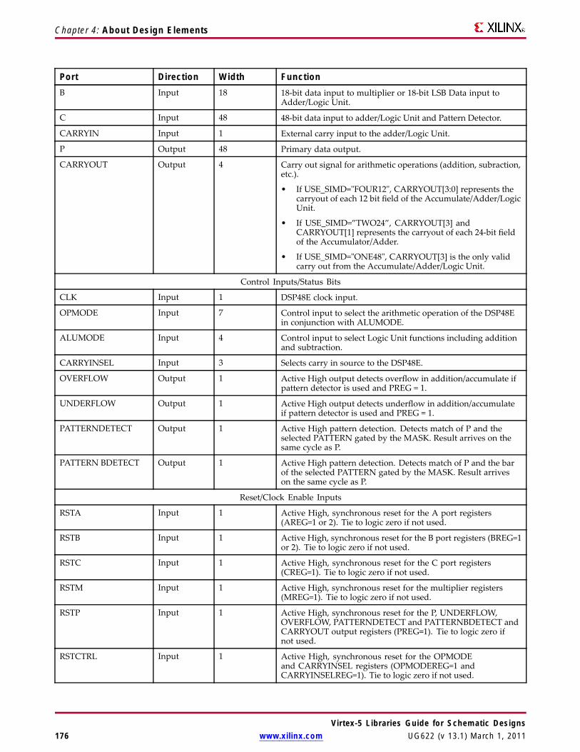
Chapter 4: About Design Elements
Port Direction Width FunctionB Input 18 18-bit data input to multiplier or 18-bit LSB Data input to
Adder/Logic Unit.
C Input 48 48-bit data input to adder/Logic Unit and Pattern Detector.
CARRYIN Input 1 External carry input to the adder/Logic Unit.
P Output 48 Primary data output.
CARRYOUT Output 4 Carry out signal for arithmetic operations (addition, subraction,etc.).
• If USE_SIMD="FOUR12", CARRYOUT[3:0] represents thecarryout of each 12 bit field of the Accumulate/Adder/LogicUnit.
• If USE_SIMD=”TWO24”, CARRYOUT[3] andCARRYOUT[1] represents the carryout of each 24-bit fieldof the Accumulator/Adder.
• If USE_SIMD="ONE48", CARRYOUT[3] is the only validcarry out from the Accumulate/Adder/Logic Unit.
Control Inputs/Status Bits
CLK Input 1 DSP48E clock input.
OPMODE Input 7 Control input to select the arithmetic operation of the DSP48Ein conjunction with ALUMODE.
ALUMODE Input 4 Control input to select Logic Unit functions including additionand subtraction.
CARRYINSEL Input 3 Selects carry in source to the DSP48E.
OVERFLOW Output 1 Active High output detects overflow in addition/accumulate ifpattern detector is used and PREG = 1.
UNDERFLOW Output 1 Active High output detects underflow in addition/accumulateif pattern detector is used and PREG = 1.
PATTERNDETECT Output 1 Active High pattern detection. Detects match of P and theselected PATTERN gated by the MASK. Result arrives on thesame cycle as P.
PATTERN BDETECT Output 1 Active High pattern detection. Detects match of P and the barof the selected PATTERN gated by the MASK. Result arriveson the same cycle as P.
Reset/Clock Enable Inputs
RSTA Input 1 Active High, synchronous reset for the A port registers(AREG=1 or 2). Tie to logic zero if not used.
RSTB Input 1 Active High, synchronous reset for the B port registers (BREG=1or 2). Tie to logic zero if not used.
RSTC Input 1 Active High, synchronous reset for the C port registers(CREG=1). Tie to logic zero if not used.
RSTM Input 1 Active High, synchronous reset for the multiplier registers(MREG=1). Tie to logic zero if not used.
RSTP Input 1 Active High, synchronous reset for the P, UNDERFLOW,OVERFLOW, PATTERNDETECT and PATTERNBDETECT andCARRYOUT output registers (PREG=1). Tie to logic zero ifnot used.
RSTCTRL Input 1 Active High, synchronous reset for the OPMODEand CARRYINSEL registers (OPMODEREG=1 andCARRYINSELREG=1). Tie to logic zero if not used.
Virtex-5 Libraries Guide for Schematic Designs176 www.xilinx.com UG622 (v 13.1) March 1, 2011

Chapter 4: About Design Elements
Port Direction Width FunctionRSTALLCARRYIN Input 1 Active High, synchronous reset for all carry-in registers
(CARRYINREG=1) or MULTCARRYINREG=1. Tie to logic zeroif not used.
RSTALUMODE Input 1 Active High, synchronous reset for the ALUMODE registers(ALUMODEREG=1).Tie to logic zero if not used.
CEA1 Input 1 Active High, clock enable for the A port registers (AREG=2). Tieto logic one if not used and AREG=2. Tie to logic zero if AREG=0or 1. When two registers are used, this is the first sequentially.
CEA2 Input 1 Active High, clock enable for the A port registers. Tie to logicone if not used and AREG=1 or 2. Tie to logic zero if AREG=0.When two registers are used, this is the second sequentially.
CEB1 Input 1 Active High, clock enable for the B port registers (BREG=2). Tieto logic one if not used and BREG=2. Tie to logic zero if BREG=0or 1. When two registers are used, this is the first sequentially.
CEB2 Input 1 Active High, clock enable for the B port registers. Tie to logicone if not used and BREG=1 or 2. Tie to logic zero if BREG=0.When two registers are used, this is the second sequentially.
CEC Input 1 Active High, clock enable for the C port registers (CREG=1). Tieto logic one if not used.
CEM Input 1 Active High, clock enable for the multiplier registers (MREG=1).Tie to logic one if not used.
CEP Input 1 Active High, clock enable for the output port registers (PREG=1).Tie to logic one if not used.
CECTRL Input 1 Active High, clock enable for the OPMODE and Carry-in Selectregisters (CTRLREG=1). Tie to logic one if not used.
CECARRYIN Input 1 Active High, clock enable for the Carry-in registers(CARRYINREG=1). Tie to logic one if not used.
CEMULTCARRYIN Input 1 Clock enable for internal multiply symmetric rounding carryregister. (MULTCARRYINREG=1).
CEALUMODE Input 1 Clock enable for the ALUMODE input registers(ALUMODEREG=1).
Cascade Ports
ACIN Input 30 Cascade input for Port A. If used, connect to ACOUT ofupstream cascaded DSP48E. If not used, tie port to all zeros.
BCIN Input 18 Cascade input for Port B. If used, connect to BCOUT of upstreamcascaded DSP48E. If not used, tie port to all zeros.
PCIN Input 48 Cascade input for Port P. If used, connect to PCOUT of upstreamcascaded DSP48E. If not used, tie port to all zeros.
CARRYCASCIN Input 1 Cascaded Carryout[2] from previous DSP48E.
MULTSIGNIN Input 1 Communicates multiplier sign output of a cascaded DSP48Eslice for the purpose of sign extending the adder/accumulatoroutput when greater than a 48-bit outpus is necessary. Shouldonly be connected to the MULTSIGNOUT output pin.
ACOUT Output 30 Cascade output for Port A. If used, connect to ACIN ofdownstream cascaded DSP48E. If not used, leave unconnected.
BCOUT Output 18 Cascade output for Port B. If used, connect to BCIN ofdownstream cascaded DSP48E. If not used, leave unconnected.
PCOUT Output 48 Cascade output for Port P. If used, connect to PCIN ofdownstream cascaded DSP48E. If not used, leave unconnected.
Virtex-5 Libraries Guide for Schematic DesignsUG622 (v 13.1) March 1, 2011 www.xilinx.com 177

Chapter 4: About Design Elements
Port Direction Width FunctionCARRYCASCOUT Output 1 Cascaded Carryout[3] to next DSP48.
MULTSIGNOUT Output 1 Communicates multiplier sign output to a cascadedDSP48E element for the purpose of sign extending theadder/accumulator output. Should only be connected to theMULTISIGNIN input pin.
Design Entry MethodThis design element can be used in schematics.
Available Attributes
Attribute TypeAllowedValues Default Description
ACASCREG Integer 0, 1 or 2 1 In conjunction with AREG, selects number ofA input registers on the ACIN cascade input.Must be equal to or one less than AREG value.
AREG Integer 0, 1 or 2 1 Selects whether to register the A input to theDSP48E.
ALUMODEREG Integer 0, 1 1 Selects whether to register the ALUMODEinput pins or not.
AUTORESET_PATTERN_DETECT
Boolean TRUE orFALSE
FALSE Automatically reset DSP48E P Register(accumulated value or CounterValue) on next clock cycle if patterndetect event as determined byAUTORESET_PATTERN_DETECT_OPTINV has occurred on this clock cycle.
AUTORESET_PATTERN_DETECT_OPTINV
String "MATCH","NOT_MATCH”
"MATCH” Determines if AUTORESET_PATTERN_DETECT should cause auto reset of P Registeron the next cycle A) if pattern is matched orB) whenever pattern is not matched on thecurrent cycle but was matched on the lastclock cycle.
A_INPUT String "DIRECT" or"CASCADE”
"DIRECT” Selects between A ("DIRECT") and ACIN("CASCADE") inputs.
BCASCREG Integer 0, 1, 2 1 In conjunction with BREG, selects number ofB input registers on BCIN cascade input.
BREG Integer 0, 1, 2 1 Selects whether to register the B input to theDSP48E.
B_INPUT String "DIRECT" or"CASCADE”
"DIRECT” Selects between B ("DIRECT") and BCIN("CASCADE") inputs.
CARRYINREG Integer 0, 1 1 Selects whether to register the CARRYINinput to the DSP48E.
CARRYINSELREG Integer 0, 1 1 Selects whether to register the CARRYINSELinput to the DSP48E.
CREG Integer 0, 1 1 Selects whether to register the C input to theDSP48E.
MASK Hexadecimal Any 48-BitValue
3FFF Mask to be used for pattern detector.
MREG Integer 0, 1 1 Selects whether to register the multiplier stageof the DSP48. Enable=1/disable=0.
Virtex-5 Libraries Guide for Schematic Designs178 www.xilinx.com UG622 (v 13.1) March 1, 2011

Chapter 4: About Design Elements
Attribute TypeAllowedValues Default Description
MULTCARRYINREG Integer 0, 1 1 Selects number of Internal Carry registers(used for Multiply Symmetric Roundingonly).
OPMODEREG Integer 0, 1 1 Selects whether to register the OPMODEinputs to the DSP48E.
PATTERN Hexadecimal Any 48-BitValue
All zeros Pattern to be used for pattern detector.
PREG Integer 0, 1 1 Selects whether to register the P input to theDSP48E.
SEL_MASK String "MASK", "C” "MASK” Selects whether to use the static MASK or theC input for the mask of the pattern detector.
SEL_PATTERN String "PATTERN","C”
"PATTERN” Selects whether to use the static PATTERNor the C input for the pattern of the patterndetector.
SEL_ROUNDING_MASK
String "SEL_MASK","MODE1","MODE2”
"SEL_MASK”
Selects special mask to be used for symmetricand convergent rounding uses of the patterndetector. If set to "MODE1" or "MODE2"SEL_MASK attribute is overridden. These areused for convergent rounding.
SIM_MODE String "SAFE" or"FAST"
"SAFE" This is a simulation only attribute. Itwill direct the simulation model to run inperformance-oriented mode when set to"FAST". Please see the Synthesis and SimulationDesign Guide for more information.
USE_MULT String "MULT","MULT_S","NONE”
"MULT_S” Selects usage of the Multiplier. Set to"NONE" to save power when using only theAdder/Logic Unit. Set to "MULT" if MREG isset to 0 and set to "MULT_S" if MREG is setto 1.
USE_SIMD String "ONE48","TWO24","FOUR12”
"ONE48” Selects usage of the SIMD (Single InstructionMultiple Data) Adder/Logic Unit. Selectbetween one 48-bit Logic Unit, two 24-bitLogic Unit, or four 12-bit Logic Unit. Notethat all four 12 bit Logic Unit share the sameInstruction (i.e. all can subtract on the samecycle or add on the same cycle). This doesallow the 48 bit adder to be broken up intosmaller adders for less computationallyintensive applications. SIMD only hasan effect on arithmetic operation (add,accumulate, subtract, etc.) and has no effecton logical operations.
USE_PATTERN_DETECT
String "PAT_DET","NO_PATDET"
"NO_PATDET"
Enables pattern detection. Only affectssimulation model and speed files.
For More Information• See the Virtex-5 FPGA User Guide.
• See the Virtex-5 FPGA Data Sheet DC and Switching Characteristics.
Virtex-5 Libraries Guide for Schematic DesignsUG622 (v 13.1) March 1, 2011 www.xilinx.com 179

Chapter 4: About Design Elements
FDPrimitive: D Flip-Flop
IntroductionThis design element is a D-type flip-flop with data input (D) and data output (Q). The data on the D inputs isloaded into the flip-flop during the Low-to-High clock (C) transition.
This flip-flop is asynchronously cleared, outputs Low, when power is applied. For FPGA devices, power-onconditions are simulated when global set/reset (GSR) is active. GSR defaults to active-High but can be invertedby adding an inverter in front of the GSR input of the appropriate STARTUP_architecture symbol.
Logic TableInputs Outputs
D C Q0 ↑ 0
1 ↑ 1
Design Entry MethodThis design element is only for use in schematics.
Available Attributes
Attribute TypeAllowedValues Default Description
INIT Binary 0, 1 0 Sets the initial value of Q output after configuration
For More Information• See the Virtex-5 FPGA User Guide.
• See the Virtex-5 FPGA Data Sheet DC and Switching Characteristics.
Virtex-5 Libraries Guide for Schematic Designs180 www.xilinx.com UG622 (v 13.1) March 1, 2011

Chapter 4: About Design Elements
FD_1Primitive: D Flip-Flop with Negative-Edge Clock
IntroductionThis design element is a single D-type flip-flop with data input (D) and data output (Q). The data on the (D)input is loaded into the flip-flop during the High-to-Low clock (C) transition.
This flip-flop is asynchronously cleared, outputs Low, when power is applied. For FPGA devices, power-onconditions are simulated when global set/reset (GSR) is active. GSR defaults to active-High but can be invertedby adding an inverter in front of the GSR input of the appropriate STARTUP_architecture symbol.
Logic TableInputs OutputsD C Q
0 ↓ 0
1 ↓ 1
Design Entry MethodThis design element is only for use in schematics.
Available Attributes
Attribute TypeAllowedValues Default Description
INIT Binary 0, 1 0 Sets the initial value of Q output after configuration
For More Information• See the Virtex-5 FPGA User Guide.
• See the Virtex-5 FPGA Data Sheet DC and Switching Characteristics.
Virtex-5 Libraries Guide for Schematic DesignsUG622 (v 13.1) March 1, 2011 www.xilinx.com 181
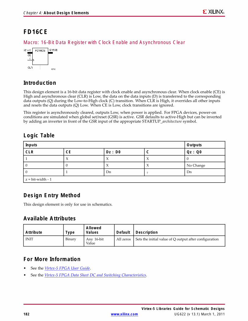
Chapter 4: About Design Elements
FD16CEMacro: 16-Bit Data Register with Clock Enable and Asynchronous Clear
IntroductionThis design element is a 16-bit data register with clock enable and asynchronous clear. When clock enable (CE) isHigh and asynchronous clear (CLR) is Low, the data on the data inputs (D) is transferred to the correspondingdata outputs (Q) during the Low-to-High clock (C) transition. When CLR is High, it overrides all other inputsand resets the data outputs (Q) Low. When CE is Low, clock transitions are ignored.
This register is asynchronously cleared, outputs Low, when power is applied. For FPGA devices, power-onconditions are simulated when global set/reset (GSR) is active. GSR defaults to active-High but can be invertedby adding an inverter in front of the GSR input of the appropriate STARTUP_architecture symbol.
Logic TableInputs Outputs
CLR CE Dz : D0 C Qz : Q01 X X X 0
0 0 X X No Change
0 1 Dn ↑ Dn
z = bit-width - 1
Design Entry MethodThis design element is only for use in schematics.
Available Attributes
Attribute TypeAllowedValues Default Description
INIT Binary Any 16-bitValue
All zeros Sets the initial value of Q output after configuration
For More Information• See the Virtex-5 FPGA User Guide.
• See the Virtex-5 FPGA Data Sheet DC and Switching Characteristics.
Virtex-5 Libraries Guide for Schematic Designs182 www.xilinx.com UG622 (v 13.1) March 1, 2011
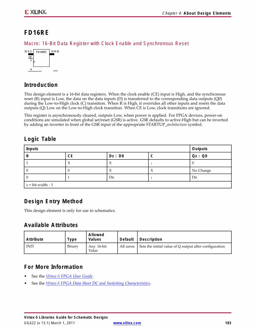
Chapter 4: About Design Elements
FD16REMacro: 16-Bit Data Register with Clock Enable and Synchronous Reset
IntroductionThis design element is a 16-bit data registers. When the clock enable (CE) input is High, and the synchronousreset (R) input is Low, the data on the data inputs (D) is transferred to the corresponding data outputs (Q0)during the Low-to-High clock (C) transition. When R is High, it overrides all other inputs and resets the dataoutputs (Q) Low on the Low-to-High clock transition. When CE is Low, clock transitions are ignored.
This register is asynchronously cleared, outputs Low, when power is applied. For FPGA devices, power-onconditions are simulated when global set/reset (GSR) is active. GSR defaults to active-High but can be invertedby adding an inverter in front of the GSR input of the appropriate STARTUP_architecture symbol.
Logic TableInputs Outputs
R CE Dz : D0 C Qz : Q01 X X ↑ 0
0 0 X X No Change
0 1 Dn ↑ Dn
z = bit-width - 1
Design Entry MethodThis design element is only for use in schematics.
Available Attributes
Attribute TypeAllowedValues Default Description
INIT Binary Any 16-bitValue
All zeros Sets the initial value of Q output after configuration
For More Information• See the Virtex-5 FPGA User Guide.
• See the Virtex-5 FPGA Data Sheet DC and Switching Characteristics.
Virtex-5 Libraries Guide for Schematic DesignsUG622 (v 13.1) March 1, 2011 www.xilinx.com 183

Chapter 4: About Design Elements
FD4CEMacro: 4-Bit Data Register with Clock Enable and Asynchronous Clear
IntroductionThis design element is a 4-bit data register with clock enable and asynchronous clear. When clock enable (CE) isHigh and asynchronous clear (CLR) is Low, the data on the data inputs (D) is transferred to the correspondingdata outputs (Q) during the Low-to-High clock (C) transition. When CLR is High, it overrides all other inputsand resets the data outputs (Q) Low. When CE is Low, clock transitions are ignored.
This register is asynchronously cleared, outputs Low, when power is applied. For FPGA devices, power-onconditions are simulated when global set/reset (GSR) is active. GSR defaults to active-High but can be invertedby adding an inverter in front of the GSR input of the appropriate STARTUP_architecture symbol.
Logic TableInputs Outputs
CLR CE Dz : D0 C Qz : Q01 X X X 0
0 0 X X No Change
0 1 Dn ↑ Dn
z = bit-width - 1
Design Entry MethodThis design element is only for use in schematics.
Available AttributesAttribute Type Allowed Values Default DescriptionINIT Binary Any 4-Bit Value All zeros Sets the initial value of Q output after
configuration.
For More Information• See the Virtex-5 FPGA User Guide.
• See the Virtex-5 FPGA Data Sheet DC and Switching Characteristics.
Virtex-5 Libraries Guide for Schematic Designs184 www.xilinx.com UG622 (v 13.1) March 1, 2011

Chapter 4: About Design Elements
FD4REMacro: 4-Bit Data Register with Clock Enable and Synchronous Reset
IntroductionThis design element is a 4-bit data registers. When the clock enable (CE) input is High, and the synchronous reset(R) input is Low, the data on the data inputs (D) is transferred to the corresponding data outputs (Q0) during theLow-to-High clock (C) transition. When R is High, it overrides all other inputs and resets the data outputs (Q)Low on the Low-to-High clock transition. When CE is Low, clock transitions are ignored.
This register is asynchronously cleared, outputs Low, when power is applied. For FPGA devices, power-onconditions are simulated when global set/reset (GSR) is active. GSR defaults to active-High but can be invertedby adding an inverter in front of the GSR input of the appropriate STARTUP_architecture symbol.
Logic TableInputs Outputs
R CE Dz : D0 C Qz : Q01 X X ↑ 0
0 0 X X No Change
0 1 Dn ↑ Dn
z = bit-width - 1
Design Entry MethodThis design element is only for use in schematics.
Available AttributesAttribute Type Allowed Values Default DescriptionINIT Binary Any 4-Bit Value All zeros Sets the initial value of Q output after
configuration.
For More Information• See the Virtex-5 FPGA User Guide.
• See the Virtex-5 FPGA Data Sheet DC and Switching Characteristics.
Virtex-5 Libraries Guide for Schematic DesignsUG622 (v 13.1) March 1, 2011 www.xilinx.com 185
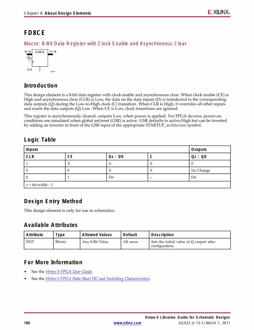
Chapter 4: About Design Elements
FD8CEMacro: 8-Bit Data Register with Clock Enable and Asynchronous Clear
IntroductionThis design element is a 8-bit data register with clock enable and asynchronous clear. When clock enable (CE) isHigh and asynchronous clear (CLR) is Low, the data on the data inputs (D) is transferred to the correspondingdata outputs (Q) during the Low-to-High clock (C) transition. When CLR is High, it overrides all other inputsand resets the data outputs (Q) Low. When CE is Low, clock transitions are ignored.
This register is asynchronously cleared, outputs Low, when power is applied. For FPGA devices, power-onconditions are simulated when global set/reset (GSR) is active. GSR defaults to active-High but can be invertedby adding an inverter in front of the GSR input of the appropriate STARTUP_architecture symbol.
Logic TableInputs Outputs
CLR CE Dz : D0 C Qz : Q01 X X X 0
0 0 X X No Change
0 1 Dn ↑ Dn
z = bit-width - 1
Design Entry MethodThis design element is only for use in schematics.
Available AttributesAttribute Type Allowed Values Default DescriptionINIT Binary Any 8-Bit Value All zeros Sets the initial value of Q output after
configuration.
For More Information• See the Virtex-5 FPGA User Guide.
• See the Virtex-5 FPGA Data Sheet DC and Switching Characteristics.
Virtex-5 Libraries Guide for Schematic Designs186 www.xilinx.com UG622 (v 13.1) March 1, 2011

Chapter 4: About Design Elements
FD8REMacro: 8-Bit Data Register with Clock Enable and Synchronous Reset
IntroductionThis design element is an 8-bit data register. When the clock enable (CE) input is High, and the synchronous reset(R) input is Low, the data on the data inputs (D) is transferred to the corresponding data outputs (Q0) during theLow-to-High clock (C) transition. When R is High, it overrides all other inputs and resets the data outputs (Q)Low on the Low-to-High clock transition. When CE is Low, clock transitions are ignored.
This register is asynchronously cleared, outputs Low, when power is applied. For FPGA devices, power-onconditions are simulated when global set/reset (GSR) is active. GSR defaults to active-High but can be invertedby adding an inverter in front of the GSR input of the appropriate STARTUP_architecture symbol.
Logic TableInputs Outputs
R CE Dz : D0 C Qz : Q01 X X ↑ 0
0 0 X X No Change
0 1 Dn ↑ Dn
z = bit-width - 1
Design Entry MethodThis design element is only for use in schematics.
Available AttributesAttribute Type Allowed Values Default DescriptionINIT Binary Any 8-Bit Value All zeros Sets the initial value of Q output after
configuration.
For More Information• See the Virtex-5 FPGA User Guide.
• See the Virtex-5 FPGA Data Sheet DC and Switching Characteristics.
Virtex-5 Libraries Guide for Schematic DesignsUG622 (v 13.1) March 1, 2011 www.xilinx.com 187
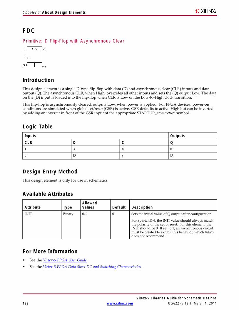
Chapter 4: About Design Elements
FDCPrimitive: D Flip-Flop with Asynchronous Clear
IntroductionThis design element is a single D-type flip-flop with data (D) and asynchronous clear (CLR) inputs and dataoutput (Q). The asynchronous CLR, when High, overrides all other inputs and sets the (Q) output Low. The dataon the (D) input is loaded into the flip-flop when CLR is Low on the Low-to-High clock transition.
This flip-flop is asynchronously cleared, outputs Low, when power is applied. For FPGA devices, power-onconditions are simulated when global set/reset (GSR) is active. GSR defaults to active-High but can be invertedby adding an inverter in front of the GSR input of the appropriate STARTUP_architecture symbol.
Logic TableInputs Outputs
CLR D C Q1 X X 0
0 D ↑ D
Design Entry MethodThis design element is only for use in schematics.
Available Attributes
Attribute TypeAllowedValues Default Description
INIT Binary 0, 1 0 Sets the initial value of Q output after configuration
For Spartan®-6, the INIT value should always matchthe polarity of the set or reset. For this element, theINIT should be 0. If set to 1, an asynchronous circuitmust be created to exhibit this behavior, which Xilinxdoes not recommend.
For More Information• See the Virtex-5 FPGA User Guide.
• See the Virtex-5 FPGA Data Sheet DC and Switching Characteristics.
Virtex-5 Libraries Guide for Schematic Designs188 www.xilinx.com UG622 (v 13.1) March 1, 2011
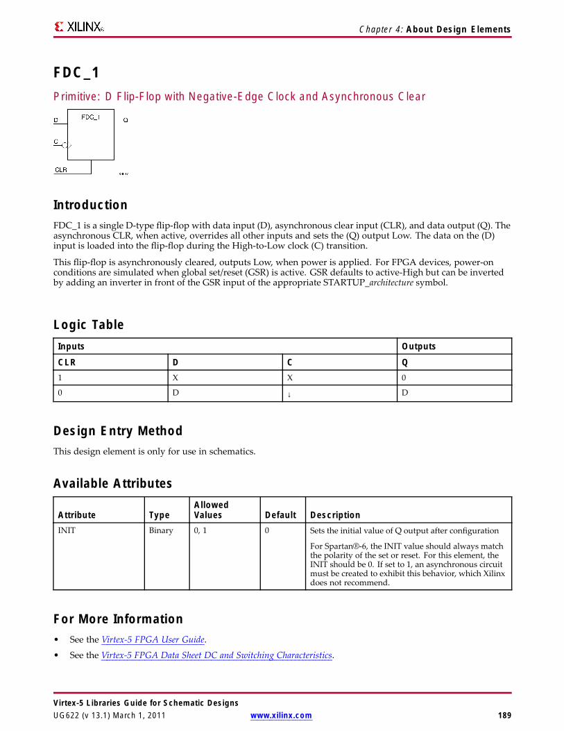
Chapter 4: About Design Elements
FDC_1Primitive: D Flip-Flop with Negative-Edge Clock and Asynchronous Clear
IntroductionFDC_1 is a single D-type flip-flop with data input (D), asynchronous clear input (CLR), and data output (Q). Theasynchronous CLR, when active, overrides all other inputs and sets the (Q) output Low. The data on the (D)input is loaded into the flip-flop during the High-to-Low clock (C) transition.
This flip-flop is asynchronously cleared, outputs Low, when power is applied. For FPGA devices, power-onconditions are simulated when global set/reset (GSR) is active. GSR defaults to active-High but can be invertedby adding an inverter in front of the GSR input of the appropriate STARTUP_architecture symbol.
Logic TableInputs Outputs
CLR D C Q1 X X 0
0 D ↓ D
Design Entry MethodThis design element is only for use in schematics.
Available Attributes
Attribute TypeAllowedValues Default Description
INIT Binary 0, 1 0 Sets the initial value of Q output after configuration
For Spartan®-6, the INIT value should always matchthe polarity of the set or reset. For this element, theINIT should be 0. If set to 1, an asynchronous circuitmust be created to exhibit this behavior, which Xilinxdoes not recommend.
For More Information• See the Virtex-5 FPGA User Guide.
• See the Virtex-5 FPGA Data Sheet DC and Switching Characteristics.
Virtex-5 Libraries Guide for Schematic DesignsUG622 (v 13.1) March 1, 2011 www.xilinx.com 189
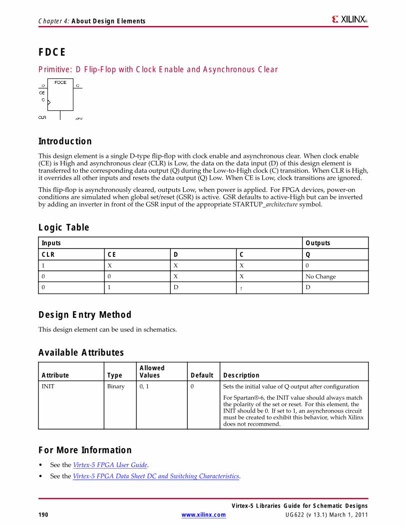
Chapter 4: About Design Elements
FDCEPrimitive: D Flip-Flop with Clock Enable and Asynchronous Clear
IntroductionThis design element is a single D-type flip-flop with clock enable and asynchronous clear. When clock enable(CE) is High and asynchronous clear (CLR) is Low, the data on the data input (D) of this design element istransferred to the corresponding data output (Q) during the Low-to-High clock (C) transition. When CLR is High,it overrides all other inputs and resets the data output (Q) Low. When CE is Low, clock transitions are ignored.
This flip-flop is asynchronously cleared, outputs Low, when power is applied. For FPGA devices, power-onconditions are simulated when global set/reset (GSR) is active. GSR defaults to active-High but can be invertedby adding an inverter in front of the GSR input of the appropriate STARTUP_architecture symbol.
Logic TableInputs Outputs
CLR CE D C Q1 X X X 0
0 0 X X No Change
0 1 D ↑ D
Design Entry MethodThis design element can be used in schematics.
Available Attributes
Attribute TypeAllowedValues Default Description
INIT Binary 0, 1 0 Sets the initial value of Q output after configuration
For Spartan®-6, the INIT value should always matchthe polarity of the set or reset. For this element, theINIT should be 0. If set to 1, an asynchronous circuitmust be created to exhibit this behavior, which Xilinxdoes not recommend.
For More Information• See the Virtex-5 FPGA User Guide.
• See the Virtex-5 FPGA Data Sheet DC and Switching Characteristics.
Virtex-5 Libraries Guide for Schematic Designs190 www.xilinx.com UG622 (v 13.1) March 1, 2011
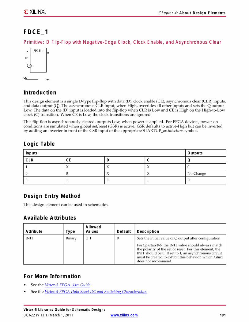
Chapter 4: About Design Elements
FDCE_1Primitive: D Flip-Flop with Negative-Edge Clock, Clock Enable, and Asynchronous Clear
IntroductionThis design element is a single D-type flip-flop with data (D), clock enable (CE), asynchronous clear (CLR) inputs,and data output (Q). The asynchronous CLR input, when High, overrides all other inputs and sets the Q outputLow. The data on the (D) input is loaded into the flip-flop when CLR is Low and CE is High on the High-to-Lowclock (C) transition. When CE is Low, the clock transitions are ignored.
This flip-flop is asynchronously cleared, outputs Low, when power is applied. For FPGA devices, power-onconditions are simulated when global set/reset (GSR) is active. GSR defaults to active-High but can be invertedby adding an inverter in front of the GSR input of the appropriate STARTUP_architecture symbol.
Logic TableInputs Outputs
CLR CE D C Q1 X X X 0
0 0 X X No Change
0 1 D ↓ D
Design Entry MethodThis design element can be used in schematics.
Available Attributes
Attribute TypeAllowedValues Default Description
INIT Binary 0, 1 0 Sets the initial value of Q output after configuration
For Spartan®-6, the INIT value should always matchthe polarity of the set or reset. For this element, theINIT should be 0. If set to 1, an asynchronous circuitmust be created to exhibit this behavior, which Xilinxdoes not recommend.
For More Information• See the Virtex-5 FPGA User Guide.• See the Virtex-5 FPGA Data Sheet DC and Switching Characteristics.
Virtex-5 Libraries Guide for Schematic DesignsUG622 (v 13.1) March 1, 2011 www.xilinx.com 191
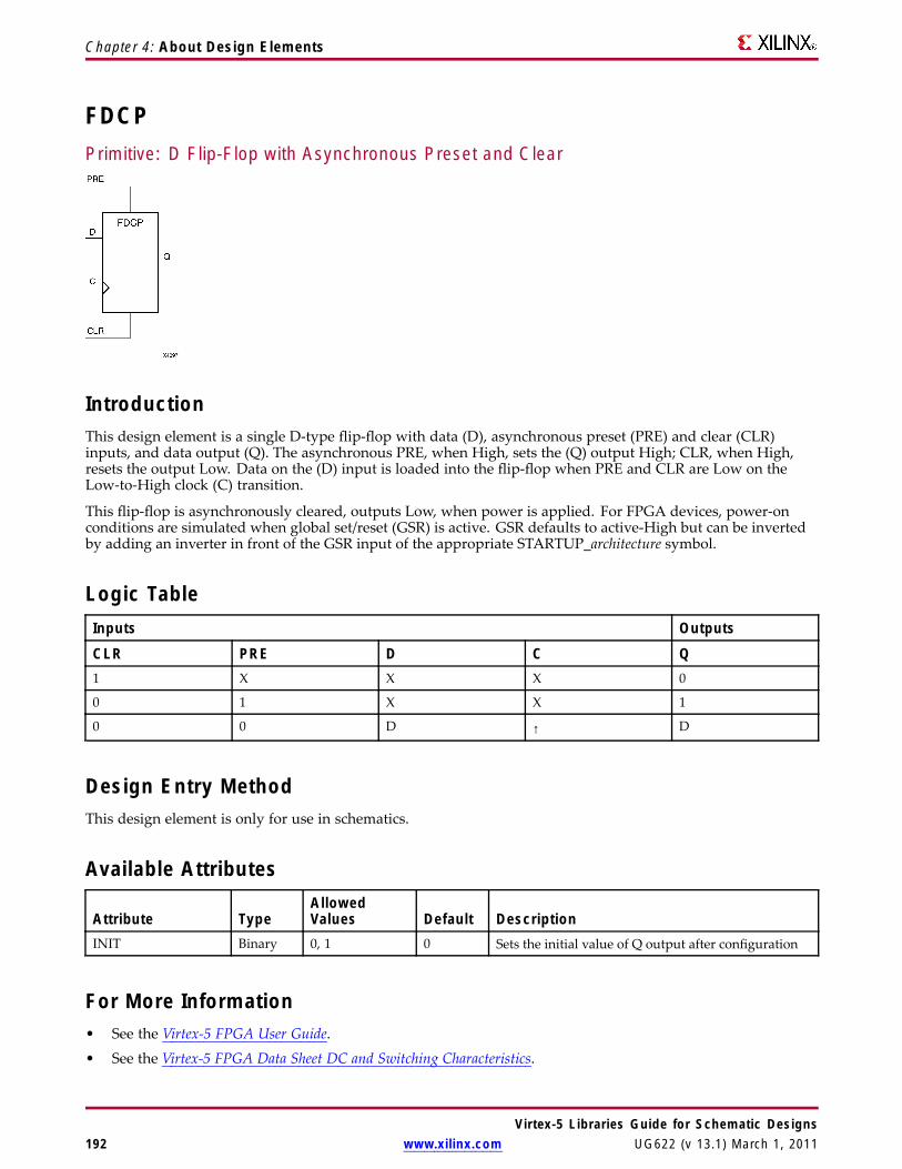
Chapter 4: About Design Elements
FDCPPrimitive: D Flip-Flop with Asynchronous Preset and Clear
IntroductionThis design element is a single D-type flip-flop with data (D), asynchronous preset (PRE) and clear (CLR)inputs, and data output (Q). The asynchronous PRE, when High, sets the (Q) output High; CLR, when High,resets the output Low. Data on the (D) input is loaded into the flip-flop when PRE and CLR are Low on theLow-to-High clock (C) transition.
This flip-flop is asynchronously cleared, outputs Low, when power is applied. For FPGA devices, power-onconditions are simulated when global set/reset (GSR) is active. GSR defaults to active-High but can be invertedby adding an inverter in front of the GSR input of the appropriate STARTUP_architecture symbol.
Logic TableInputs Outputs
CLR PRE D C Q1 X X X 0
0 1 X X 1
0 0 D ↑ D
Design Entry MethodThis design element is only for use in schematics.
Available Attributes
Attribute TypeAllowedValues Default Description
INIT Binary 0, 1 0 Sets the initial value of Q output after configuration
For More Information• See the Virtex-5 FPGA User Guide.
• See the Virtex-5 FPGA Data Sheet DC and Switching Characteristics.
Virtex-5 Libraries Guide for Schematic Designs192 www.xilinx.com UG622 (v 13.1) March 1, 2011

Chapter 4: About Design Elements
FDCP_1Primitive: D Flip-Flop with Negative-Edge Clock and Asynchronous Preset and Clear
IntroductionThis design element is a single D-type flip-flop with data (D), asynchronous preset (PRE) and clear (CLR)inputs, and data output (Q). The asynchronous PRE, when High, sets the (Q) output High; CLR, when High,resets the output Low. Data on the (D) input is loaded into the flip-flop when PRE and CLR are Low on theHigh-to-Low clock (C) transition.
This flip-flop is asynchronously cleared, outputs Low, when power is applied. For FPGA devices, power-onconditions are simulated when global set/reset (GSR) is active. GSR defaults to active-High but can be invertedby adding an inverter in front of the GSR input of the appropriate STARTUP_architecture symbol.
Logic TableInputs Outputs
CLR PRE D C Q1 X X X 0
0 1 X X 1
0 0 0 ↓ 0
0 0 1 ↓ 1
Design Entry MethodThis design element is only for use in schematics.
Available Attributes
Attribute TypeAllowedValues Default Description
INIT Binary 0, 1 0 Sets the initial value of Q output after configuration
For More Information• See the Virtex-5 FPGA User Guide.
• See the Virtex-5 FPGA Data Sheet DC and Switching Characteristics.
Virtex-5 Libraries Guide for Schematic DesignsUG622 (v 13.1) March 1, 2011 www.xilinx.com 193
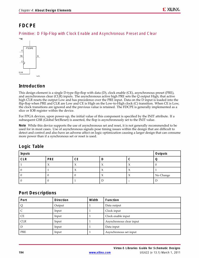
Chapter 4: About Design Elements
FDCPEPrimitive: D Flip-Flop with Clock Enable and Asynchronous Preset and Clear
IntroductionThis design element is a single D-type flip-flop with data (D), clock enable (CE), asynchronous preset (PRE),and asynchronous clear (CLR) inputs. The asynchronous active high PRE sets the Q output High; that activehigh CLR resets the output Low and has precedence over the PRE input. Data on the D input is loaded into theflip-flop when PRE and CLR are Low and CE is High on the Low-to-High clock (C) transition. When CE is Low,the clock transitions are ignored and the previous value is retained. The FDCPE is generally implemented as aslice or IOB register within the device.
For FPGA devices, upon power-up, the initial value of this component is specified by the INIT attribute. If asubsequent GSR (Global Set/Reset) is asserted, the flop is asynchronously set to the INIT value.
Note While this device supports the use of asynchronous set and reset, it is not generally recommended to beused for in most cases. Use of asynchronous signals pose timing issues within the design that are difficult todetect and control and also have an adverse affect on logic optimization causing a larger design that can consumemore power than if a synchronous set or reset is used.
Logic TableInputs Outputs
CLR PRE CE D C Q1 X X X X 0
0 1 X X X 1
0 0 0 X X No Change
0 0 1 D ↑ D
Port DescriptionsPort Direction Width FunctionQ Output 1 Data output
C Input 1 Clock input
CE Input 1 Clock enable input
CLR Input 1 Asynchronous clear input
D Input 1 Data input
PRE Input 1 Asynchronous set input
Virtex-5 Libraries Guide for Schematic Designs194 www.xilinx.com UG622 (v 13.1) March 1, 2011

Chapter 4: About Design Elements
Design Entry MethodThis design element can be used in schematics.
Available Attributes
Attribute TypeAllowedValues Default Description
INIT Binary 0,1 0 Sets the initial value of Q output after configurationand on GSR.
For More Information• See the Virtex-5 FPGA User Guide.
• See the Virtex-5 FPGA Data Sheet DC and Switching Characteristics.
Virtex-5 Libraries Guide for Schematic DesignsUG622 (v 13.1) March 1, 2011 www.xilinx.com 195

Chapter 4: About Design Elements
FDCPE_1Primitive: D Flip-Flop with Negative-Edge Clock, Clock Enable, and Asynchronous Presetand Clear
IntroductionFDCPE_1 is a single D-type flip-flop with data (D), clock enable (CE), asynchronous preset (PRE), andasynchronous clear (CLR) inputs and data output (Q). The asynchronous PRE, when High, sets the (Q) outputHigh; CLR, when High, resets the output Low. Data on the (D) input is loaded into the flip-flop when PRE andCLR are Low and CE is High on the High-to-Low clock (C) transition. When CE is Low, the clock transitionsare ignored.
This flip-flop is asynchronously cleared, outputs Low, when power is applied. For FPGA devices, power-onconditions are simulated when global set/reset (GSR) is active. GSR defaults to active-High but can be invertedby adding an inverter in front of the GSR input of the appropriate STARTUP_architecture symbol.
Logic TableInputs Outputs
CLR PRE CE D C Q1 X X X X 0
0 1 X X X 1
0 0 0 X X No Change
0 0 1 D ↓ D
Port DescriptionsPort Direction Width FunctionQ Output 1 Data output
C Input 1 Clock input
CE Input 1 Clock enable input
CLR Input 1 Asynchronous clear input
D Input 1 Data input
PRE Input 1 Asynchronous set input
Design Entry MethodThis design element can be used in schematics.
Virtex-5 Libraries Guide for Schematic Designs196 www.xilinx.com UG622 (v 13.1) March 1, 2011

Chapter 4: About Design Elements
Available Attributes
Attribute TypeAllowedValues Default Description
INIT Binary 0,1 0 Sets the initial value of Q output after configurationand on GSR.
For More Information• See the Virtex-5 FPGA User Guide.
• See the Virtex-5 FPGA Data Sheet DC and Switching Characteristics.
Virtex-5 Libraries Guide for Schematic DesignsUG622 (v 13.1) March 1, 2011 www.xilinx.com 197

Chapter 4: About Design Elements
FDEPrimitive: D Flip-Flop with Clock Enable
IntroductionThis design element is a single D-type flip-flop with data input (D), clock enable (CE), and data output (Q).When clock enable is High, the data on the (D) input is loaded into the flip-flop during the Low-to-High clock(C) transition.
This flip-flop is asynchronously cleared, outputs Low, when power is applied. For FPGA devices, power-onconditions are simulated when global set/reset (GSR) is active. GSR defaults to active-High but can be invertedby adding an inverter in front of the GSR input of the appropriate STARTUP_architecture symbol.
Logic TableInputs Outputs
CE D C Q0 X X No Change
1 0 ↑ 0
1 1 ↑ 1
Design Entry MethodThis design element is only for use in schematics.
Available Attributes
Attribute TypeAllowedValues Default Description
INIT Binary 0, 1 0 Sets the initial value of Q output after configuration
For More Information• See the Virtex-5 FPGA User Guide.
• See the Virtex-5 FPGA Data Sheet DC and Switching Characteristics.
Virtex-5 Libraries Guide for Schematic Designs198 www.xilinx.com UG622 (v 13.1) March 1, 2011

Chapter 4: About Design Elements
FDE_1Primitive: D Flip-Flop with Negative-Edge Clock and Clock Enable
IntroductionThis design element is a single D-type flip-flop with data input (D), clock enable (CE), and data output (Q).When clock enable is High, the data on the (D) input is loaded into the flip-flop during the High-to-Low clock(C) transition.
This flip-flop is asynchronously cleared, outputs Low, when power is applied. For FPGA devices, power-onconditions are simulated when global set/reset (GSR) is active. GSR defaults to active-High but can be invertedby adding an inverter in front of the GSR input of the appropriate STARTUP_architecture symbol.
Logic TableInputs Outputs
CE D C Q0 X X No Change
1 0 ↓ 0
1 1 ↓ 1
Design Entry MethodThis design element is only for use in schematics.
Available Attributes
Attribute TypeAllowedValues Default Description
INIT Binary 0, 1 0 Sets the initial value of Q output after configuration
For More Information• See the Virtex-5 FPGA User Guide.
• See the Virtex-5 FPGA Data Sheet DC and Switching Characteristics.
Virtex-5 Libraries Guide for Schematic DesignsUG622 (v 13.1) March 1, 2011 www.xilinx.com 199
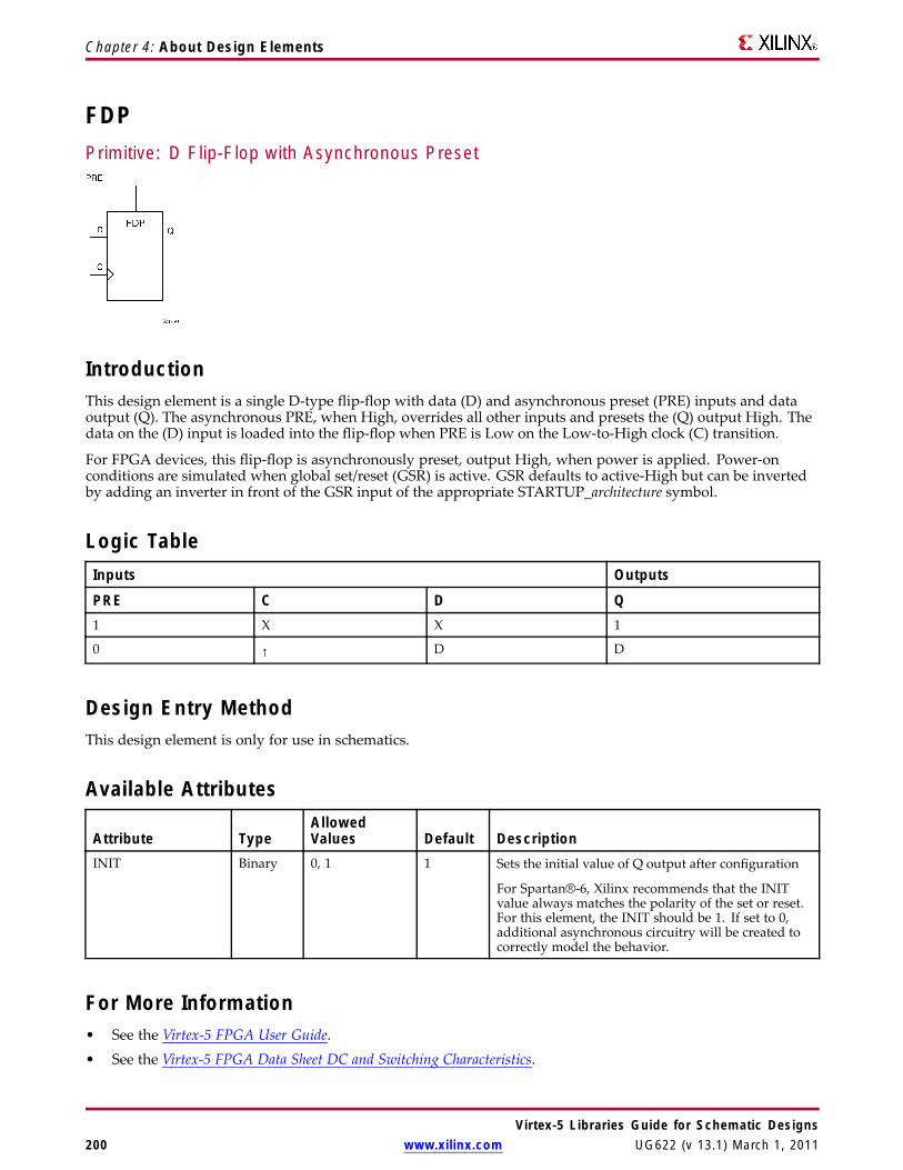
Chapter 4: About Design Elements
FDPPrimitive: D Flip-Flop with Asynchronous Preset
IntroductionThis design element is a single D-type flip-flop with data (D) and asynchronous preset (PRE) inputs and dataoutput (Q). The asynchronous PRE, when High, overrides all other inputs and presets the (Q) output High. Thedata on the (D) input is loaded into the flip-flop when PRE is Low on the Low-to-High clock (C) transition.
For FPGA devices, this flip-flop is asynchronously preset, output High, when power is applied. Power-onconditions are simulated when global set/reset (GSR) is active. GSR defaults to active-High but can be invertedby adding an inverter in front of the GSR input of the appropriate STARTUP_architecture symbol.
Logic TableInputs Outputs
PRE C D Q1 X X 1
0 ↑ D D
Design Entry MethodThis design element is only for use in schematics.
Available Attributes
Attribute TypeAllowedValues Default Description
INIT Binary 0, 1 1 Sets the initial value of Q output after configuration
For Spartan®-6, Xilinx recommends that the INITvalue always matches the polarity of the set or reset.For this element, the INIT should be 1. If set to 0,additional asynchronous circuitry will be created tocorrectly model the behavior.
For More Information• See the Virtex-5 FPGA User Guide.• See the Virtex-5 FPGA Data Sheet DC and Switching Characteristics.
Virtex-5 Libraries Guide for Schematic Designs200 www.xilinx.com UG622 (v 13.1) March 1, 2011

Chapter 4: About Design Elements
FDP_1Primitive: D Flip-Flop with Negative-Edge Clock and Asynchronous Preset
IntroductionThis design element is a single D-type flip-flop with data (D) and asynchronous preset (PRE) inputs and dataoutput (Q). The asynchronous PRE, when High, overrides all other inputs and presets the Q output High. Thedata on the D input is loaded into the flip-flop when PRE is Low on the High-to-Low clock (C) transition.
This flip-flop is asynchronously preset, output High, when power is applied. For FPGA devices, power-onconditions are simulated when global set/reset (GSR) is active. GSR defaults to active-High but can be invertedby adding an inverter in front of the GSR input of the appropriate STARTUP_architecture symbol.
Logic TableInputs Outputs
PRE C D Q1 X X 1
0 ↓ D D
Design Entry MethodThis design element is only for use in schematics.
Available Attributes
Attribute TypeAllowedValues Default Description
INIT Binary 0, 1 1 Sets the initial value of Q output after configuration
For Spartan®-6, Xilinx recommends that the INITvalue always matches the polarity of the set or reset.For this element, the INIT should be 1. If set to 0,additional asynchronous circuitry will be created tocorrectly model the behavior.
For More Information• See the Virtex-5 FPGA User Guide.• See the Virtex-5 FPGA Data Sheet DC and Switching Characteristics.
Virtex-5 Libraries Guide for Schematic DesignsUG622 (v 13.1) March 1, 2011 www.xilinx.com 201
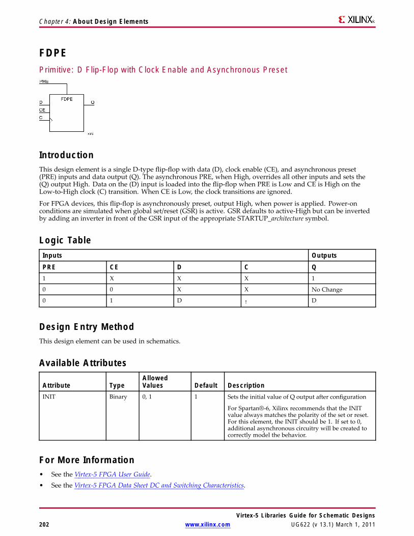
Chapter 4: About Design Elements
FDPEPrimitive: D Flip-Flop with Clock Enable and Asynchronous Preset
IntroductionThis design element is a single D-type flip-flop with data (D), clock enable (CE), and asynchronous preset(PRE) inputs and data output (Q). The asynchronous PRE, when High, overrides all other inputs and sets the(Q) output High. Data on the (D) input is loaded into the flip-flop when PRE is Low and CE is High on theLow-to-High clock (C) transition. When CE is Low, the clock transitions are ignored.
For FPGA devices, this flip-flop is asynchronously preset, output High, when power is applied. Power-onconditions are simulated when global set/reset (GSR) is active. GSR defaults to active-High but can be invertedby adding an inverter in front of the GSR input of the appropriate STARTUP_architecture symbol.
Logic TableInputs Outputs
PRE CE D C Q1 X X X 1
0 0 X X No Change
0 1 D ↑ D
Design Entry MethodThis design element can be used in schematics.
Available Attributes
Attribute TypeAllowedValues Default Description
INIT Binary 0, 1 1 Sets the initial value of Q output after configuration
For Spartan®-6, Xilinx recommends that the INITvalue always matches the polarity of the set or reset.For this element, the INIT should be 1. If set to 0,additional asynchronous circuitry will be created tocorrectly model the behavior.
For More Information• See the Virtex-5 FPGA User Guide.• See the Virtex-5 FPGA Data Sheet DC and Switching Characteristics.
Virtex-5 Libraries Guide for Schematic Designs202 www.xilinx.com UG622 (v 13.1) March 1, 2011
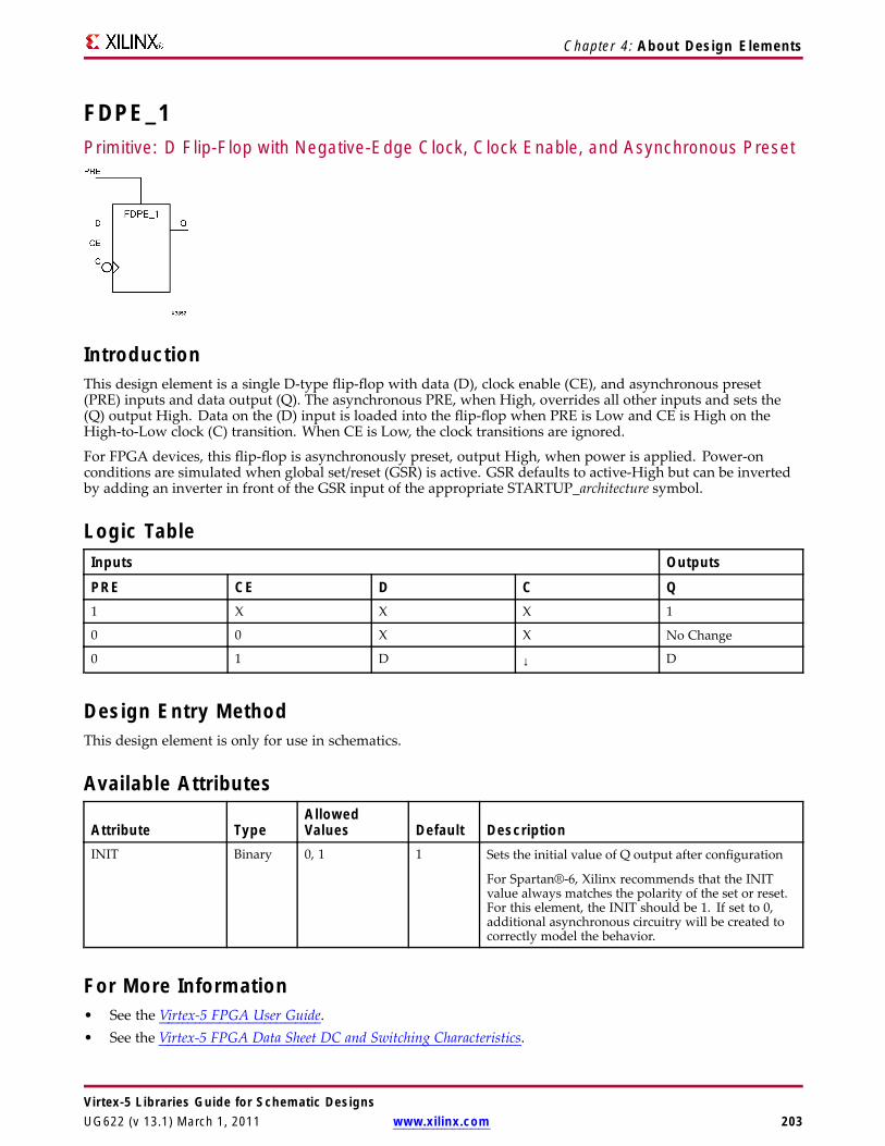
Chapter 4: About Design Elements
FDPE_1Primitive: D Flip-Flop with Negative-Edge Clock, Clock Enable, and Asynchronous Preset
IntroductionThis design element is a single D-type flip-flop with data (D), clock enable (CE), and asynchronous preset(PRE) inputs and data output (Q). The asynchronous PRE, when High, overrides all other inputs and sets the(Q) output High. Data on the (D) input is loaded into the flip-flop when PRE is Low and CE is High on theHigh-to-Low clock (C) transition. When CE is Low, the clock transitions are ignored.
For FPGA devices, this flip-flop is asynchronously preset, output High, when power is applied. Power-onconditions are simulated when global set/reset (GSR) is active. GSR defaults to active-High but can be invertedby adding an inverter in front of the GSR input of the appropriate STARTUP_architecture symbol.
Logic TableInputs Outputs
PRE CE D C Q1 X X X 1
0 0 X X No Change
0 1 D ↓ D
Design Entry MethodThis design element is only for use in schematics.
Available Attributes
Attribute TypeAllowedValues Default Description
INIT Binary 0, 1 1 Sets the initial value of Q output after configuration
For Spartan®-6, Xilinx recommends that the INITvalue always matches the polarity of the set or reset.For this element, the INIT should be 1. If set to 0,additional asynchronous circuitry will be created tocorrectly model the behavior.
For More Information• See the Virtex-5 FPGA User Guide.• See the Virtex-5 FPGA Data Sheet DC and Switching Characteristics.
Virtex-5 Libraries Guide for Schematic DesignsUG622 (v 13.1) March 1, 2011 www.xilinx.com 203

Chapter 4: About Design Elements
FDRPrimitive: D Flip-Flop with Synchronous Reset
IntroductionThis design element is a single D-type flip-flop with data (D) and synchronous reset (R) inputs and data output(Q). The synchronous reset (R) input, when High, overrides all other inputs and resets the (Q) output Low onthe Low-to-High clock (C) transition. The data on the (D) input is loaded into the flip-flop when R is Lowduring the Low-to- High clock transition.
This flip-flop is asynchronously cleared, outputs Low, when power is applied. For FPGA devices, power-onconditions are simulated when global set/reset (GSR) is active. GSR defaults to active-High but can be invertedby adding an inverter in front of the GSR input of the appropriate STARTUP_architecture symbol.
Logic TableInputs Outputs
R D C Q1 X ↑ 0
0 D ↑ D
Design Entry MethodThis design element is only for use in schematics.
Available Attributes
Attribute TypeAllowedValues Default Description
INIT Binary 0, 1 0 Sets the initial value of Q output after configuration
For More Information• See the Virtex-5 FPGA User Guide.
• See the Virtex-5 FPGA Data Sheet DC and Switching Characteristics.
Virtex-5 Libraries Guide for Schematic Designs204 www.xilinx.com UG622 (v 13.1) March 1, 2011

Chapter 4: About Design Elements
FDR_1Primitive: D Flip-Flop with Negative-Edge Clock and Synchronous Reset
IntroductionThis design element is a single D-type flip-flop with data (D) and synchronous reset (R) inputs and data output(Q). The synchronous reset (R) input, when High, overrides all other inputs and resets the (Q) output Low onthe High-to-Low clock (C) transition. The data on the (D) input is loaded into the flip-flop when R is Lowduring the High-to- Low clock transition.
This flip-flop is asynchronously cleared, outputs Low, when power is applied. For FPGA devices, power-onconditions are simulated when global set/reset (GSR) is active. GSR defaults to active-High but can be invertedby adding an inverter in front of the GSR input of the appropriate STARTUP_architecture symbol.
Logic TableInputs Outputs
R D C Q1 X ↓ 0
0 D ↓ D
Design Entry MethodThis design element is only for use in schematics.
Available Attributes
Attribute TypeAllowedValues Default Description
INIT Binary 0, 1 0 Sets the initial value of Q output after configuration
For More Information• See the Virtex-5 FPGA User Guide.
• See the Virtex-5 FPGA Data Sheet DC and Switching Characteristics.
Virtex-5 Libraries Guide for Schematic DesignsUG622 (v 13.1) March 1, 2011 www.xilinx.com 205

Chapter 4: About Design Elements
FDREPrimitive: D Flip-Flop with Clock Enable and Synchronous Reset
IntroductionThis design element is a single D-type flip-flop with data (D), clock enable (CE), and synchronous reset (R) inputsand data output (Q). The synchronous reset (R) input, when High, overrides all other inputs and resets the (Q)output Low on the Low-to-High clock (C) transition. The data on the (D) input is loaded into the flip-flop when Ris Low and CE is High during the Low-to-High clock transition.
This flip-flop is asynchronously cleared, outputs Low, when power is applied. For FPGA devices, power-onconditions are simulated when global set/reset (GSR) is active. GSR defaults to active-High but can be invertedby adding an inverter in front of the GSR input of the appropriate STARTUP_architecture symbol.
Logic TableInputs Outputs
R CE D C Q1 X X ↑ 0
0 0 X X No Change
0 1 D ↑ D
Design Entry MethodThis design element can be used in schematics.
Available Attributes
Attribute TypeAllowedValues Default Description
INIT Binary 0, 1 0 Sets the initial value of Q output after configuration
For Spartan®-6, the INIT value should always matchthe polarity of the set or reset. For this element, theINIT should be 0. If set to 1, an asynchronous circuitmust be created to exhibit this behavior, which Xilinxdoes not recommend.
For More Information• See the Virtex-5 FPGA User Guide.• See the Virtex-5 FPGA Data Sheet DC and Switching Characteristics.
Virtex-5 Libraries Guide for Schematic Designs206 www.xilinx.com UG622 (v 13.1) March 1, 2011
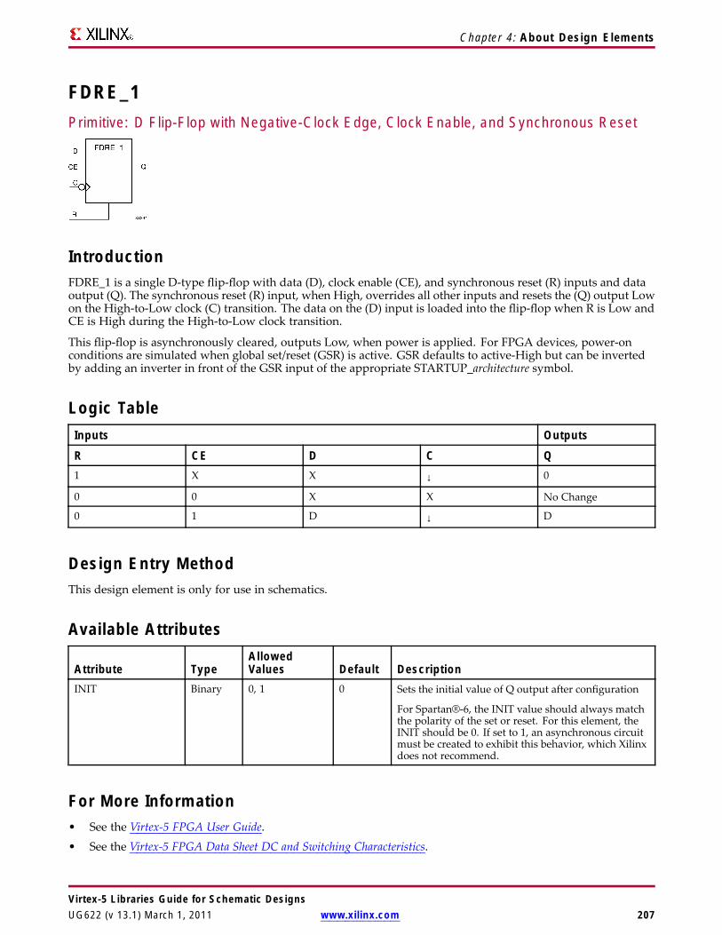
Chapter 4: About Design Elements
FDRE_1Primitive: D Flip-Flop with Negative-Clock Edge, Clock Enable, and Synchronous Reset
IntroductionFDRE_1 is a single D-type flip-flop with data (D), clock enable (CE), and synchronous reset (R) inputs and dataoutput (Q). The synchronous reset (R) input, when High, overrides all other inputs and resets the (Q) output Lowon the High-to-Low clock (C) transition. The data on the (D) input is loaded into the flip-flop when R is Low andCE is High during the High-to-Low clock transition.
This flip-flop is asynchronously cleared, outputs Low, when power is applied. For FPGA devices, power-onconditions are simulated when global set/reset (GSR) is active. GSR defaults to active-High but can be invertedby adding an inverter in front of the GSR input of the appropriate STARTUP_architecture symbol.
Logic TableInputs Outputs
R CE D C Q1 X X ↓ 0
0 0 X X No Change
0 1 D ↓ D
Design Entry MethodThis design element is only for use in schematics.
Available Attributes
Attribute TypeAllowedValues Default Description
INIT Binary 0, 1 0 Sets the initial value of Q output after configuration
For Spartan®-6, the INIT value should always matchthe polarity of the set or reset. For this element, theINIT should be 0. If set to 1, an asynchronous circuitmust be created to exhibit this behavior, which Xilinxdoes not recommend.
For More Information• See the Virtex-5 FPGA User Guide.• See the Virtex-5 FPGA Data Sheet DC and Switching Characteristics.
Virtex-5 Libraries Guide for Schematic DesignsUG622 (v 13.1) March 1, 2011 www.xilinx.com 207

Chapter 4: About Design Elements
FDRSPrimitive: D Flip-Flop with Synchronous Reset and Set
IntroductionFDRS is a single D-type flip-flop with data (D), synchronous set (S), and synchronous reset (R) inputs and dataoutput (Q). The synchronous reset (R) input, when High, overrides all other inputs and resets the (Q) output Lowduring the Low-to-High clock (C) transition. (Reset has precedence over Set.) When S is High and R is Low, theflip-flop is set, output High, during the Low-to-High clock transition. When R and S are Low, data on the (D)input is loaded into the flip-flop during the Low-to-High clock transition.
This flip-flop is asynchronously cleared, outputs Low, when power is applied. For FPGA devices, power-onconditions are simulated when global set/reset (GSR) is active. GSR defaults to active-High but can be invertedby adding an inverter in front of the GSR input of the appropriate STARTUP_architecture symbol.
Logic TableInputs Outputs
R S D C Q1 X X ↓ 0
0 1 X ↓ 1
0 0 D ↓ D
Design Entry MethodThis design element is only for use in schematics.
Available Attributes
Attribute TypeAllowedValues Default Description
INIT Binary 0, 1 0 Sets the initial value of Q output after configuration
For More Information• See the Virtex-5 FPGA User Guide.
• See the Virtex-5 FPGA Data Sheet DC and Switching Characteristics.
Virtex-5 Libraries Guide for Schematic Designs208 www.xilinx.com UG622 (v 13.1) March 1, 2011
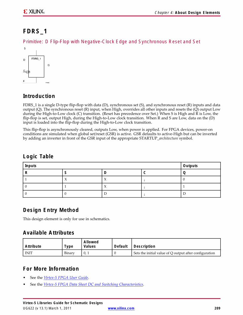
Chapter 4: About Design Elements
FDRS_1Primitive: D Flip-Flop with Negative-Clock Edge and Synchronous Reset and Set
IntroductionFDRS_1 is a single D-type flip-flop with data (D), synchronous set (S), and synchronous reset (R) inputs and dataoutput (Q). The synchronous reset (R) input, when High, overrides all other inputs and resets the (Q) output Lowduring the High-to-Low clock (C) transition. (Reset has precedence over Set.) When S is High and R is Low, theflip-flop is set, output High, during the High-to-Low clock transition. When R and S are Low, data on the (D)input is loaded into the flip-flop during the High-to-Low clock transition.
This flip-flop is asynchronously cleared, outputs Low, when power is applied. For FPGA devices, power-onconditions are simulated when global set/reset (GSR) is active. GSR defaults to active-High but can be invertedby adding an inverter in front of the GSR input of the appropriate STARTUP_architecture symbol.
Logic TableInputs Outputs
R S D C Q1 X X ↓ 0
0 1 X ↓ 1
0 0 D ↓ D
Design Entry MethodThis design element is only for use in schematics.
Available Attributes
Attribute TypeAllowedValues Default Description
INIT Binary 0, 1 0 Sets the initial value of Q output after configuration
For More Information• See the Virtex-5 FPGA User Guide.
• See the Virtex-5 FPGA Data Sheet DC and Switching Characteristics.
Virtex-5 Libraries Guide for Schematic DesignsUG622 (v 13.1) March 1, 2011 www.xilinx.com 209
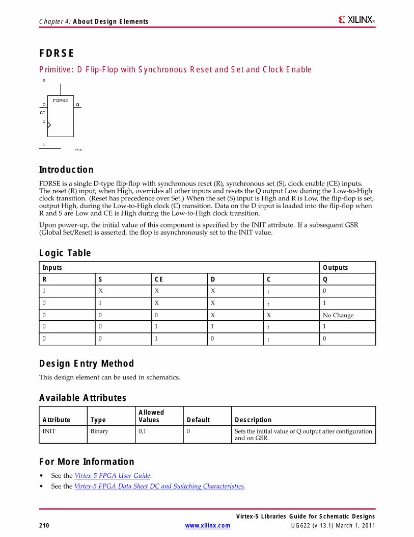
Chapter 4: About Design Elements
FDRSEPrimitive: D Flip-Flop with Synchronous Reset and Set and Clock Enable
IntroductionFDRSE is a single D-type flip-flop with synchronous reset (R), synchronous set (S), clock enable (CE) inputs.The reset (R) input, when High, overrides all other inputs and resets the Q output Low during the Low-to-Highclock transition. (Reset has precedence over Set.) When the set (S) input is High and R is Low, the flip-flop is set,output High, during the Low-to-High clock (C) transition. Data on the D input is loaded into the flip-flop whenR and S are Low and CE is High during the Low-to-High clock transition.
Upon power-up, the initial value of this component is specified by the INIT attribute. If a subsequent GSR(Global Set/Reset) is asserted, the flop is asynchronously set to the INIT value.
Logic TableInputs Outputs
R S CE D C Q1 X X X ↑ 0
0 1 X X ↑ 1
0 0 0 X X No Change
0 0 1 1 ↑ 1
0 0 1 0 ↑ 0
Design Entry MethodThis design element can be used in schematics.
Available Attributes
Attribute TypeAllowedValues Default Description
INIT Binary 0,1 0 Sets the initial value of Q output after configurationand on GSR.
For More Information• See the Virtex-5 FPGA User Guide.• See the Virtex-5 FPGA Data Sheet DC and Switching Characteristics.
Virtex-5 Libraries Guide for Schematic Designs210 www.xilinx.com UG622 (v 13.1) March 1, 2011

Chapter 4: About Design Elements
FDRSE_1Primitive: D Flip-Flop with Negative-Clock Edge, Synchronous Reset and Set, and ClockEnable
IntroductionFDRSE_1 is a single D-type flip-flop with synchronous reset (R), synchronous set (S), and clock enable (CE)inputs and data output (Q). The reset (R) input, when High, overrides all other inputs and resets the (Q) outputLow during the High-to-Low clock transition. (Reset has precedence over Set.) When the set (S) input is Highand R is Low, the flip-flop is set, output High, during the High-to-Low clock (C) transition. Data on the (D) inputis loaded into the flip-flop when (R) and (S) are Low and (CE) is High during the High-to-Low clock transition.
This flip-flop is asynchronously cleared, outputs Low, when power is applied. For FPGA devices, power-onconditions are simulated when global set/reset (GSR) is active. GSR defaults to active-High but can be invertedby adding an inverter in front of the GSR input of the appropriate STARTUP_architecture symbol.
Logic TableInputs Outputs
R S CE D C Q1 X X X ↓ 0
0 1 X X ↓ 1
0 0 0 X X No Change
0 0 1 D ↓ D
Design Entry MethodThis design element can be used in schematics.
Available Attributes
Attribute TypeAllowedValues Default Description
INIT Binary 0,1 0 Sets the initial value of Q output after configurationand on GSR.
For More Information• See the Virtex-5 FPGA User Guide.• See the Virtex-5 FPGA Data Sheet DC and Switching Characteristics.
Virtex-5 Libraries Guide for Schematic DesignsUG622 (v 13.1) March 1, 2011 www.xilinx.com 211

Chapter 4: About Design Elements
FDSPrimitive: D Flip-Flop with Synchronous Set
IntroductionFDS is a single D-type flip-flop with data (D) and synchronous set (S) inputs and data output (Q). Thesynchronous set input, when High, sets the Q output High on the Low-to-High clock (C) transition. The data onthe D input is loaded into the flip-flop when S is Low during the Low-to-High clock (C) transition.
For FPGA devices, this flip-flop is asynchronously preset, output High, when power is applied. Power-onconditions are simulated when global set/reset (GSR) is active. GSR defaults to active-High but can be invertedby adding an inverter in front of the GSR input of the appropriate STARTUP_architecture symbol.
Logic TableInputs Outputs
S D C Q1 X ↑ 1
0 D ↑ D
Design Entry MethodThis design element is only for use in schematics.
Available Attributes
Attribute TypeAllowedValues Default Description
INIT Binary 0, 1 1 Sets the initial value of Q output after configuration.
For More Information• See the Virtex-5 FPGA User Guide.
• See the Virtex-5 FPGA Data Sheet DC and Switching Characteristics.
Virtex-5 Libraries Guide for Schematic Designs212 www.xilinx.com UG622 (v 13.1) March 1, 2011
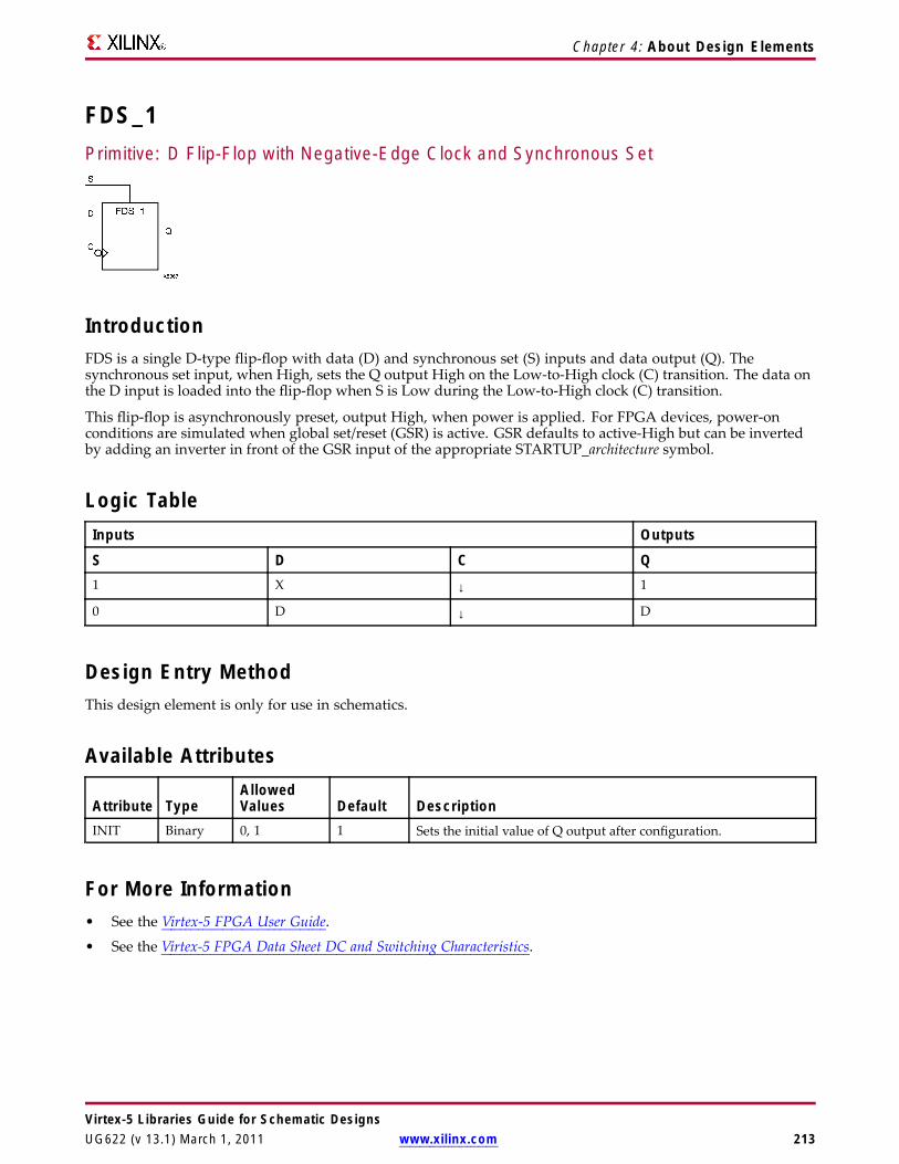
Chapter 4: About Design Elements
FDS_1Primitive: D Flip-Flop with Negative-Edge Clock and Synchronous Set
IntroductionFDS is a single D-type flip-flop with data (D) and synchronous set (S) inputs and data output (Q). Thesynchronous set input, when High, sets the Q output High on the Low-to-High clock (C) transition. The data onthe D input is loaded into the flip-flop when S is Low during the Low-to-High clock (C) transition.
This flip-flop is asynchronously preset, output High, when power is applied. For FPGA devices, power-onconditions are simulated when global set/reset (GSR) is active. GSR defaults to active-High but can be invertedby adding an inverter in front of the GSR input of the appropriate STARTUP_architecture symbol.
Logic TableInputs Outputs
S D C Q1 X ↓ 1
0 D ↓ D
Design Entry MethodThis design element is only for use in schematics.
Available Attributes
Attribute TypeAllowedValues Default Description
INIT Binary 0, 1 1 Sets the initial value of Q output after configuration.
For More Information• See the Virtex-5 FPGA User Guide.
• See the Virtex-5 FPGA Data Sheet DC and Switching Characteristics.
Virtex-5 Libraries Guide for Schematic DesignsUG622 (v 13.1) March 1, 2011 www.xilinx.com 213

Chapter 4: About Design Elements
FDSEPrimitive: D Flip-Flop with Clock Enable and Synchronous Set
IntroductionFDSE is a single D-type flip-flop with data (D), clock enable (CE), and synchronous set (S) inputs and data output(Q). The synchronous set (S) input, when High, overrides the clock enable (CE) input and sets the Q output Highduring the Low-to-High clock (C) transition. The data on the D input is loaded into the flip-flop when S is Lowand CE is High during the Low-to-High clock (C) transition.
For FPGA devices, this flip-flop is asynchronously preset, output High, when power is applied. Power-onconditions are simulated when global set/reset (GSR) is active. GSR defaults to active-High but can be invertedby adding an inverter in front of the GSR input of the appropriate STARTUP_architecture symbol.
Logic TableInputs Outputs
S CE D C Q1 X X ↑ 1
0 0 X X No Change
0 1 D ↑ D
Design Entry MethodThis design element can be used in schematics.
Available Attributes
Attribute TypeAllowedValues Default Description
INIT Binary 0, 1 1 Sets the initial value of Q output after configuration
For Spartan®-6, Xilinx recommends that the INITvalue always matches the polarity of the set or reset.For this element, the INIT should be 1. If set to 0,additional asynchronous circuitry will be created tocorrectly model the behavior.
For More Information• See the Virtex-5 FPGA User Guide.• See the Virtex-5 FPGA Data Sheet DC and Switching Characteristics.
Virtex-5 Libraries Guide for Schematic Designs214 www.xilinx.com UG622 (v 13.1) March 1, 2011

Chapter 4: About Design Elements
FDSE_1Primitive: D Flip-Flop with Negative-Edge Clock, Clock Enable, and Synchronous Set
IntroductionFDSE_1 is a single D-type flip-flop with data (D), clock enable (CE), and synchronous set (S) inputs and dataoutput (Q). The synchronous set (S) input, when High, overrides the clock enable (CE) input and sets the Qoutput High during the High-to-Low clock (C) transition. The data on the D input is loaded into the flip-flopwhen S is Low and CE is High during the High-to-Low clock (C) transition.
This flip-flop is asynchronously preset, output High, when power is applied. For FPGA devices, power-onconditions are simulated when global set/reset (GSR) is active. GSR defaults to active-High but can be invertedby adding an inverter in front of the GSR input of the appropriate STARTUP_architecture symbol.
Logic TableInputs Outputs
S CE D C Q1 X X ↓ 1
0 0 X X No Change
0 1 D ↓ D
Design Entry MethodThis design element is only for use in schematics.
Available Attributes
Attribute TypeAllowedValues Default Description
INIT Binary 0, 1 1 Sets the initial value of Q output after configuration
For Spartan®-6, Xilinx recommends that the INITvalue always matches the polarity of the set or reset.For this element, the INIT should be 1. If set to 0,additional asynchronous circuitry will be created tocorrectly model the behavior.
For More Information• See the Virtex-5 FPGA User Guide.• See the Virtex-5 FPGA Data Sheet DC and Switching Characteristics.
Virtex-5 Libraries Guide for Schematic DesignsUG622 (v 13.1) March 1, 2011 www.xilinx.com 215
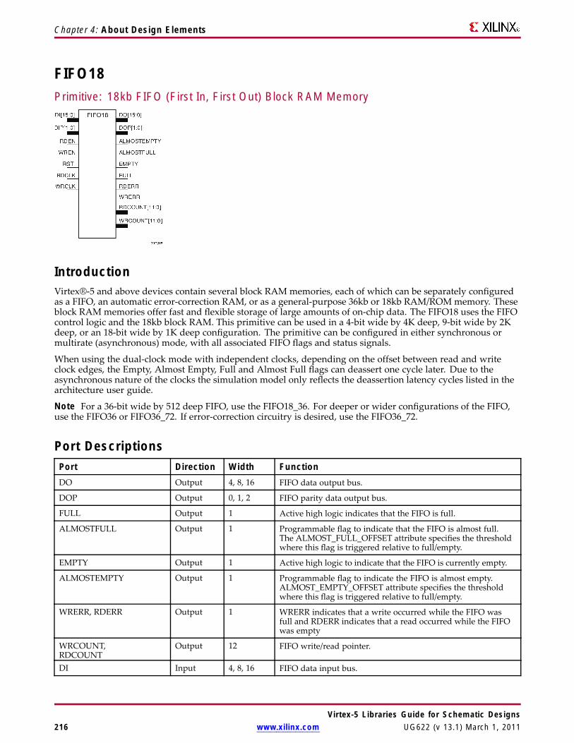
Chapter 4: About Design Elements
FIFO18Primitive: 18kb FIFO (First In, First Out) Block RAM Memory
IntroductionVirtex®-5 and above devices contain several block RAM memories, each of which can be separately configuredas a FIFO, an automatic error-correction RAM, or as a general-purpose 36kb or 18kb RAM/ROMmemory. Theseblock RAMmemories offer fast and flexible storage of large amounts of on-chip data. The FIFO18 uses the FIFOcontrol logic and the 18kb block RAM. This primitive can be used in a 4-bit wide by 4K deep, 9-bit wide by 2Kdeep, or an 18-bit wide by 1K deep configuration. The primitive can be configured in either synchronous ormultirate (asynchronous) mode, with all associated FIFO flags and status signals.
When using the dual-clock mode with independent clocks, depending on the offset between read and writeclock edges, the Empty, Almost Empty, Full and Almost Full flags can deassert one cycle later. Due to theasynchronous nature of the clocks the simulation model only reflects the deassertion latency cycles listed in thearchitecture user guide.
Note For a 36-bit wide by 512 deep FIFO, use the FIFO18_36. For deeper or wider configurations of the FIFO,use the FIFO36 or FIFO36_72. If error-correction circuitry is desired, use the FIFO36_72.
Port DescriptionsPort Direction Width FunctionDO Output 4, 8, 16 FIFO data output bus.
DOP Output 0, 1, 2 FIFO parity data output bus.
FULL Output 1 Active high logic indicates that the FIFO is full.
ALMOSTFULL Output 1 Programmable flag to indicate that the FIFO is almost full.The ALMOST_FULL_OFFSET attribute specifies the thresholdwhere this flag is triggered relative to full/empty.
EMPTY Output 1 Active high logic to indicate that the FIFO is currently empty.
ALMOSTEMPTY Output 1 Programmable flag to indicate the FIFO is almost empty.ALMOST_EMPTY_OFFSET attribute specifies the thresholdwhere this flag is triggered relative to full/empty.
WRERR, RDERR Output 1 WRERR indicates that a write occurred while the FIFO wasfull and RDERR indicates that a read occurred while the FIFOwas empty
WRCOUNT,RDCOUNT
Output 12 FIFO write/read pointer.
DI Input 4, 8, 16 FIFO data input bus.
Virtex-5 Libraries Guide for Schematic Designs216 www.xilinx.com UG622 (v 13.1) March 1, 2011
Chapter 4: About Design Elements
Port Direction Width FunctionDIP Input 0, 1, 2 FIFO parity data input bus.
WREN Input 1 Active high FIFO write enable.
RDEN Input 1 Active high FIFO read enable.
RST Input 1 Asynchronous reset (active high) of all FIFO functions, flags,and pointers. RESET must be asserted for three clock cycles.
WRCLK, RDCLK Input 1 FIFO read and write clocks (positive edge triggered).
Design Entry MethodThis design element can be used in schematics.
When you want to instantiate this primitive configured in the 4-bit WIDTH mode, connect the DIP port to logiczeros and leave the DOP port unconnected. Connect DI[3:0] and DO[3:0] to the appropriate input and outputsignals and tie DI[15:4] to logic zeros and leave DO[15:4] unconnected.
When configuring in the 9-bit WIDTH mode, connect the DIP[0] port to the appropriate data input and theDIP[1] to a logic zero. Connect DOP[0] to the appropriate data out and leave DOP[1] unconnected. ConnectDI[7:0] and DO[7:0] to the appropriate input and output signals and tie DI[15:8] to logic zeros and leaveDO[15:8] unconnected.
When configuring in the 18-bit WIDTH mode, all DI, DIP, DO and DOP signals can be connected.
For any configuration, any unused DI or DIP inputs should be tied to a logic zero, and any unused DO or DOPpins should be left unconnected. When the FIFO is set to be synchronous (EN_SYN attribute is set to TRUE),the same clock source must be tied to WRCLK and RDCLK. When in asynchronous mode (EN_SYN is set toFALSE), unique clock signals can be used. Depending on the offset between read and write clock edges, theEmpty, Almost Empty, Full and Almost Full flags can deassert one cycle later. Due to the asynchronous nature ofthe clocks the simulation model only reflects the deassertion latency cycles listed in the architecture user guide.
The FIFO must be RST after power up. The FULL, ALMOSTFULL, EMPTY and ALMOSTEMPTY outputflags should be connected to the appropriate destination logic or left unconnected if not used. The WRERR,RDERR, WRCOUNT and RDCOUNT are optional outputs and can be left unconnected if not needed. Set allattributes to the FIFO to enable the desired behavior of the primitive by adjusting the generics (VHDL) or in-linedefparams (Verilog) in the instantiation.
Available Attributes
Attribute TypeAllowedValues Default Description
ALMOST_FULL_OFFSET
Hexadecimal Any 12-Bit Value All zeros Specifies the amount of data contents in theRAM to trigger the ALMOST_FULL flag.
ALMOST_EMPTY_OFFSET
Hexadecimal Any 12-Bit Value All zeros Specifies the amount of data contents in theRAM to trigger the ALMOST_EMPTY flag.
FIRST_WORD_FALL_THROUGH
Boolean TRUE, FALSE FALSE If TRUE, the first write to the FIFO willappear on DO without a first RDENassertion.
DATA_WIDTH Integer 4, 9, 18 4 Specifies the desired data width for theFIFO.
EN_SYN Boolean TRUE, FALSE FALSE EN_SYN denotes whether the FIFOis operating in either multirate (twoindependent clocks) or synchronous (asingle clock) mode. Multirate must useDO_REG=1.
Virtex-5 Libraries Guide for Schematic DesignsUG622 (v 13.1) March 1, 2011 www.xilinx.com 217

Chapter 4: About Design Elements
Attribute TypeAllowedValues Default Description
DO_REG Integer 0, 1 1 Data pipeline register for EN_SYN.
SIM_MODE String "SAFE", "FAST" "SAFE" This is a simulation only attribute. It willdirect the simulation model to run inperformance-oriented mode when set to"FAST".
Note Not all features are supported whenset to “FAST”. Please see the Synthesisand Simulation Design Guide for moreinformation.
For More Information• See the Virtex-5 FPGA User Guide.
• See the Virtex-5 FPGA Data Sheet DC and Switching Characteristics.
Virtex-5 Libraries Guide for Schematic Designs218 www.xilinx.com UG622 (v 13.1) March 1, 2011

Chapter 4: About Design Elements
FIFO18_36Primitive: 36-bit Wide by 512 Deep 18kb FIFO (First In, First Out) Block RAM Memory
IntroductionVirtex®-5 devices contain several block RAM memories that can be configured as FIFOs, automaticerror-correction RAM, or general-purpose 36kb or 18kb RAM/ROM memories. These block RAM memoriesoffer fast and flexible storage of large amounts of on-chip data. The FIFO18_36 allows access to the blockRAM in the 18kb FIFO configuration when a wide data path is needed. This component is set to a 36-bit wide,512 deep ration with configurable synchronous or asynchronous operation. This FIFO RAM also supplies allassociated FIFO flags and status signals.
When using the dual-clock mode with independent clocks, depending on the offset between read and writeclock edges, the Empty, Almost Empty, Full and Almost Full flags can deassert one cycle later. Due to theasynchronous nature of the clocks the simulation model only reflects the deassertion latency cycles listed in thearchitecture user guide.
Note For an 18kb FIFO in a deeper, less wide configuration, use the FIFO18 component. For deeper or widerconfigurations of the FIFO, use the FIFO36 or FIFO36_72 components. If you want error-correction circuitry, useFIFO36_72.
Port DescriptionsPort Direction Width FunctionDO Output 32 FIFO data output bus.
DOP Output 4 FIFO parity data output bus.
FULL Output 1 Active high logic indicates that the FIFO contents are full.
ALMOSTFULL Output 1 Programmable flag to indicate the FIFO is almost full.ALMOST_FULL_OFFSET attribute specifies where to trigger this flag.
EMPTY Output 1 Active high logic indicates the FIFO is currently empty.
ALMOSTEMPTY Output 1 Programmable flag to indicate the FIFO is almost empty.ALMOST_EMPTY_OFFSET attribute specifies where to trigger thisflag.
WRERR, RDERR Output 1 WRERR indicates that a write occurred while the FIFO was full whileRDERR indicated a read occurred while the FIFO was empty
WRCOUNT,RDCOUNT
Output 9 FIFO write/read pointer.
Virtex-5 Libraries Guide for Schematic DesignsUG622 (v 13.1) March 1, 2011 www.xilinx.com 219
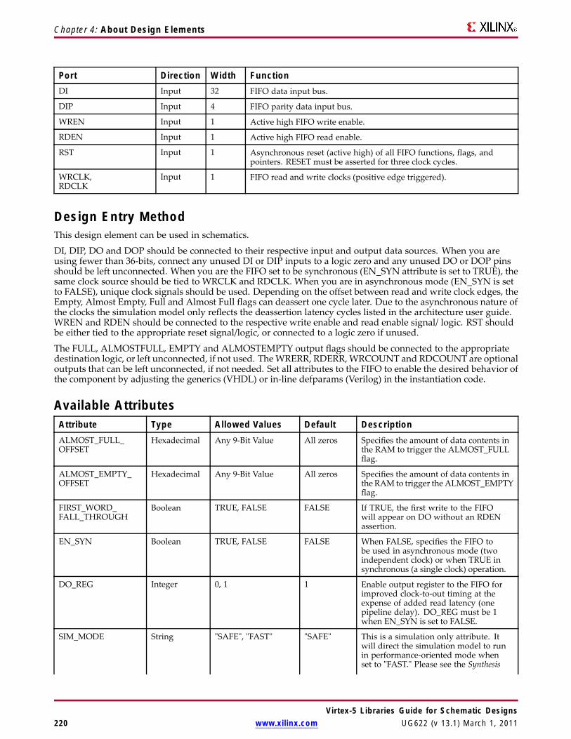
Chapter 4: About Design Elements
Port Direction Width FunctionDI Input 32 FIFO data input bus.
DIP Input 4 FIFO parity data input bus.
WREN Input 1 Active high FIFO write enable.
RDEN Input 1 Active high FIFO read enable.
RST Input 1 Asynchronous reset (active high) of all FIFO functions, flags, andpointers. RESET must be asserted for three clock cycles.
WRCLK,RDCLK
Input 1 FIFO read and write clocks (positive edge triggered).
Design Entry MethodThis design element can be used in schematics.
DI, DIP, DO and DOP should be connected to their respective input and output data sources. When you areusing fewer than 36-bits, connect any unused DI or DIP inputs to a logic zero and any unused DO or DOP pinsshould be left unconnected. When you are the FIFO set to be synchronous (EN_SYN attribute is set to TRUE), thesame clock source should be tied to WRCLK and RDCLK. When you are in asynchronous mode (EN_SYN is setto FALSE), unique clock signals should be used. Depending on the offset between read and write clock edges, theEmpty, Almost Empty, Full and Almost Full flags can deassert one cycle later. Due to the asynchronous nature ofthe clocks the simulation model only reflects the deassertion latency cycles listed in the architecture user guide.WREN and RDEN should be connected to the respective write enable and read enable signal/ logic. RST shouldbe either tied to the appropriate reset signal/logic, or connected to a logic zero if unused.
The FULL, ALMOSTFULL, EMPTY and ALMOSTEMPTY output flags should be connected to the appropriatedestination logic, or left unconnected, if not used. TheWRERR, RDERR,WRCOUNT and RDCOUNT are optionaloutputs that can be left unconnected, if not needed. Set all attributes to the FIFO to enable the desired behavior ofthe component by adjusting the generics (VHDL) or in-line defparams (Verilog) in the instantiation code.
Available AttributesAttribute Type Allowed Values Default DescriptionALMOST_FULL_OFFSET
Hexadecimal Any 9-Bit Value All zeros Specifies the amount of data contents inthe RAM to trigger the ALMOST_FULLflag.
ALMOST_EMPTY_OFFSET
Hexadecimal Any 9-Bit Value All zeros Specifies the amount of data contents inthe RAM to trigger theALMOST_EMPTYflag.
FIRST_WORD_FALL_THROUGH
Boolean TRUE, FALSE FALSE If TRUE, the first write to the FIFOwill appear on DO without an RDENassertion.
EN_SYN Boolean TRUE, FALSE FALSE When FALSE, specifies the FIFO tobe used in asynchronous mode (twoindependent clock) or when TRUE insynchronous (a single clock) operation.
DO_REG Integer 0, 1 1 Enable output register to the FIFO forimproved clock-to-out timing at theexpense of added read latency (onepipeline delay). DO_REG must be 1when EN_SYN is set to FALSE.
SIM_MODE String "SAFE", "FAST" "SAFE" This is a simulation only attribute. Itwill direct the simulation model to runin performance-oriented mode whenset to "FAST." Please see the Synthesis
Virtex-5 Libraries Guide for Schematic Designs220 www.xilinx.com UG622 (v 13.1) March 1, 2011

Chapter 4: About Design Elements
Attribute Type Allowed Values Default Descriptionand Simulation Design Guide for moreinformation.
For More Information• See the Virtex-5 FPGA User Guide.
• See the Virtex-5 FPGA Data Sheet DC and Switching Characteristics.
Virtex-5 Libraries Guide for Schematic DesignsUG622 (v 13.1) March 1, 2011 www.xilinx.com 221

Chapter 4: About Design Elements
FIFO36
Primitive: 36kb FIFO (First In, First Out) Block RAM Memory
IntroductionVirtex®-5 and above devices contain several block RAM memories that can be configured as FIFOs, automaticerror-correction RAM, or general-purpose 36kb or 18kb RAM/ROM memories. These block RAM memoriesoffer fast and flexible storage of large amounts of on-chip data. The FIFO36 allows access to the block RAM inthe 36kb FIFO configurations. This component can be configured and used as a 4-bit wide by 8K deep, 9-bit by4K deep, 18-bit by 2K deep or a 36-bit wide by 1K deep synchronous or multirate (asynchronous) FIFO RAMwith all associated FIFO flags.
When using the dual-clock mode with independent clocks, depending on the offset between read and writeclock edges, the Empty, Almost Empty, Full and Almost Full flags can deassert one cycle later. Due to theasynchronous nature of the clocks the simulation model only reflects the deassertion latency cycles listed in thearchitecture user guide.
Note For a 72-bit wide by 512 deep use the FIFO, the FIFO36_72 component. For smaller configurations of theFIFO, use the FIFO18 or FIFO18_36. If error-correction circuitry is desired, use the FIFO36_72.
Port Descriptions
Port Direction Width FunctionDO Output 4, 8, 16, 32 FIFO data output bus.
DOP Output 0, 1, 2, 4 FIFO parity data output bus.
FULL Output 1 Active high logic indicates that the FIFO contents are full.
ALMOSTFULL Output 1 Programmable flag to indicate that the FIFO is almostfull. The ALMOST_FULL_OFFSET attribute specifies thethreshold where this flag is triggered relative to full/empty.
EMPTY Output 1 Active high logic indicates that the FIFO is currently empty.
ALMOSTEMPTY Output 1 Programmable flag to indicate the FIFO is almost empty.ALMOST_EMPTY_OFFSET attribute specifies the thresholdwhere this flag is triggered relative to full/empty.
WRERR, RDERR Output 1 WRERR indicates that a write occurred while the FIFO wasfull and RDERR indicates that a read occurred while theFIFO was empty.
Virtex-5 Libraries Guide for Schematic Designs222 www.xilinx.com UG622 (v 13.1) March 1, 2011
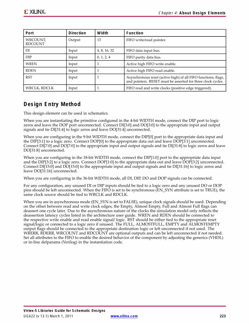
Chapter 4: About Design Elements
Port Direction Width FunctionWRCOUNT,RDCOUNT
Output 13 FIFO write/read pointer.
DI Input 4, 8, 16, 32 FIFO data input bus.
DIP Input 0, 1, 2, 4 FIFO parity data bus.
WREN Input 1 Active high FIFO write enable.
RDEN Input 1 Active high FIFO read enable.
RST Input 1 Asynchronous reset (active high) of all FIFO functions, flags,and pointers. RESET must be asserted for three clock cycles.
WRCLK, RDCLK Input 1 FIFO read and write clocks (positive edge triggered).
Design Entry MethodThis design element can be used in schematics.
When you are instantiating the primitive configured in the 4-bit WIDTH mode, connect the DIP port to logiczeros and leave the DOP port unconnected. Connect DI[3:0] and DO[3:0] to the appropriate input and outputsignals and tie DI[31:4] to logic zeros and leave DO[31:4] unconnected.
When you are configuring in the 9-bit WIDTH mode, connect the DIP[0] port to the appropriate data input andthe DIP[3:1] to a logic zero. Connect DOP[0] to the appropriate data out and leave DOP[3:1] unconnected.Connect DI[7:0] and DO[7:0] to the appropriate input and output signals and tie DI[31:8] to logic zeros and leaveDO[31:8] unconnected.
When you are configuring in the 18-bit WIDTH mode, connect the DIP[1:0] port to the appropriate data inputand the DIP[3:2] to a logic zero. Connect DOP[1:0] to the appropriate data out and leave DOP[3:2] unconnected.Connect DI[15:0] and DO[15:0] to the appropriate input and output signals and tie DI[31:16] to logic zeros andleave DO[31:16] unconnected.
When you are configuring in the 36-bit WIDTH mode, all DI, DIP, DO and DOP signals can be connected.
For any configuration, any unused DI or DIP inputs should be tied to a logic zero and any unused DO or DOPpins should be left unconnected. When the FIFO is set to be synchronous (EN_SYN attribute is set to TRUE), thesame clock source should be tied to WRCLK and RDCLK.
When you are in asynchronous mode (EN_SYN is set to FALSE), unique clock signals should be used. Dependingon the offset between read and write clock edges, the Empty, Almost Empty, Full and Almost Full flags candeassert one cycle later. Due to the asynchronous nature of the clocks the simulation model only reflects thedeassertion latency cycles listed in the architecture user guide. WREN and RDEN should be connected tothe respective write enable and read enable signal/ logic. RST should be either tied to the appropriate resetsignal/logic or connected to a logic zero if unused. The FULL, ALMOSTFULL, EMPTY and ALMOSTEMPTYoutput flags should be connected to the appropriate destination logic or left unconnected if not used. TheWRERR, RDERR, WRCOUNT and RDCOUNT are optional outputs and can be left unconnected if not needed.Set all attributes to the FIFO to enable the desired behavior of the component by adjusting the generics (VHDL)or in-line defparams (Verilog) in the instantiation code.
Virtex-5 Libraries Guide for Schematic DesignsUG622 (v 13.1) March 1, 2011 www.xilinx.com 223

Chapter 4: About Design Elements
Available Attributes
Attribute TypeAllowedValues Default Description
ALMOST_FULL_OFFSET
Hexadecimal Any 13-Bit Value All zeros Specifies the amount of data contents in theRAM to trigger the ALMOST_FULL flag.
ALMOST_EMPTY_OFFSET
Hexadecimal Any 13-Bit Value All zeros Specifies the amount of data contents in theRAM to trigger the ALMOST_EMPTY flag.
FIRST_WORD_FALL_THROUGH
Boolean TRUE, FALSE FALSE If TRUE, the first write to the FIFO willappear on DO without an RDEN assertion.
DATA_WIDTH Integer 4 to 36 4 Specifies the desired data width for the FIFO.
EN_SYN Boolean TRUE, FALSE FALSE EN_SYN denotes whether the FIFOis operating in either multirate (twoindependent clocks) or synchronous (a singleclock) mode. Multirate must use DO_REG=1.
DO_REG Integer 0, 1 1 Data pipeline register for EN_SYN.
SIM_MODE String "SAFE", "FAST" "SAFE" This is a simulation only attribute. Itwill direct the simulation model to runin performance-oriented mode when setto "FAST". Please see the Synthesis andSimulation Design Guide for more information.
For More Information• See the Virtex-5 FPGA User Guide.
• See the Virtex-5 FPGA Data Sheet DC and Switching Characteristics.
Virtex-5 Libraries Guide for Schematic Designs224 www.xilinx.com UG622 (v 13.1) March 1, 2011

Chapter 4: About Design Elements
FIFO36_72Primitive: 72-Bit Wide by 512 Deep 36kb FIFO (First In, First Out) Block RAM Memorywith ECC (Error Detection and Correction Circuitry)
IntroductionVirtex®-5 devices contain several block RAM memories that can be configured as FIFOs, automaticerror-correction RAM, or general-purpose 36kb or 18kb RAM/ROM memories. These Block RAM memoriesoffer fast and flexible storage of large amounts of on-chip data. This element allows access to the Block RAMin the 36kB FIFO configuration when a wide data path is needed. This component is set to a 72-bit wide, 512deep ration, with configurable synchronous or asynchronous operation. Error detection and correction circuitrycan also be enabled to uncover and rectify possible memory corruptions. This FIFO RAM also supplies allassociated FIFO flags and status signals.
When using the dual-clock mode with independent clocks, depending on the offset between read and writeclock edges, the Empty, Almost Empty, Full and Almost Full flags can deassert one cycle later. Due to theasynchronous nature of the clocks the simulation model only reflects the deassertion latency cycles listed in thearchitecture user guide.
Note For a 36kb FIFO in a deeper, less wide configuration, use the FIFO36 component. For smallerconfigurations of the FIFO, use the FIFO18 or FIFO18_36.
Port DescriptionsPort Direction Width FunctionDO Output 64 FIFO data output bus.
DOP Output 8 FIFO parity data output bus.
FULL Output 1 Active high logic indicates that the FIFO contents are full.
ALMOSTFULL Output 1 Programmable flag to indicate the FIFO is almost full.ALMOST_FULL_OFFSET attribute specifies where to trigger thisflag.
EMPTY Output 1 Active high logic indicates the FIFO is currently empty.
ALMOSTEMPTY Output 1 Programmable flag to indicate the FIFO is almost empty.ALMOST_EMPTY_OFFSET attribute specifies where to trigger this flag.
Virtex-5 Libraries Guide for Schematic DesignsUG622 (v 13.1) March 1, 2011 www.xilinx.com 225
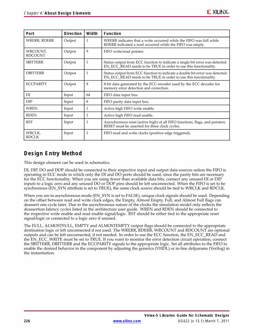
Chapter 4: About Design Elements
Port Direction Width FunctionWRERR, RDERR Output 1 WRERR indicates that a write occurred while the FIFO was full while
RDERR indicated a read occurred while the FIFO was empty.
WRCOUNT,RDCOUNT
Output 9 FIFO write/read pointer.
SBITTERR Output 1 Status output from ECC function to indicate a single bit error was detected.EN_ECC_READ needs to be TRUE in order to use this functionality.
DBITTERR Output 1 Status output from ECC function to indicate a double bit error was detected.EN_ECC_READ needs to be TRUE in order to use this functionality.
ECCPARITY Output 8 8-bit data generated by the ECC encoder used by the ECC decoder formemory error detection and correction.
DI Input 64 FIFO data input bus.
DIP Input 8 FIFO parity data input bus.
WREN Input 1 Active high FIFO write enable.
RDEN Input 1 Active high FIFO read enable.
RST Input 1 Asynchronous reset (active high) of all FIFO functions, flags, and pointers.RESET must be asserted for three clock cycles.
WRCLK,RDCLK
Input 1 FIFO read and write clocks (positive edge triggered).
Design Entry MethodThis design element can be used in schematics.
DI, DIP, DO and DOP should be connected to their respective input and output data sources unless the FIFO isoperating in ECC mode in which only the DI and DO ports should be used, since the parity bits are necessaryfor the ECC functionality. When you are using fewer than available data bits, connect any unused DI or DIPinputs to a logic zero and any unused DO or DOP pins should be left unconnected. When the FIFO is set to besynchronous (EN_SYN attribute is set to TRUE), the same clock source should be tied to WRCLK and RDCLK.
When you are in asynchronous mode (EN_SYN is set to FALSE), unique clock signals should be used. Dependingon the offset between read and write clock edges, the Empty, Almost Empty, Full, and Almost Full flags candeassert one cycle later. Due to the asynchronous nature of the clocks the simulation model only reflects thedeassertion latency cycles listed in the architecture user guide. WREN and RDEN should be connected tothe respective write enable and read enable signal/logic. RST should be either tied to the appropriate resetsignal/logic or connected to a logic zero if unused.
The FULL, ALMOSTFULL, EMPTY and ALMOSTEMPTY output flags should be connected to the appropriatedestination logic or left unconnected if not used. The WRERR, RDERR, WRCOUNT and RDCOUNT are optionaloutputs and can be left unconnected, if not needed. In order to use the ECC function, the EN_ECC_READ andthe EN_ECC_WRITE must be set to TRUE. If you want to monitor the error detection circuit operation, connectthe SBITTERR, DBITTERR and the ECCPARITY signals to the appropriate logic. Set all attributes to the FIFO toenable the desired behavior in the component by adjusting the generics (VHDL) or in-line defparams (Verilog) inthe instantiation.
Virtex-5 Libraries Guide for Schematic Designs226 www.xilinx.com UG622 (v 13.1) March 1, 2011
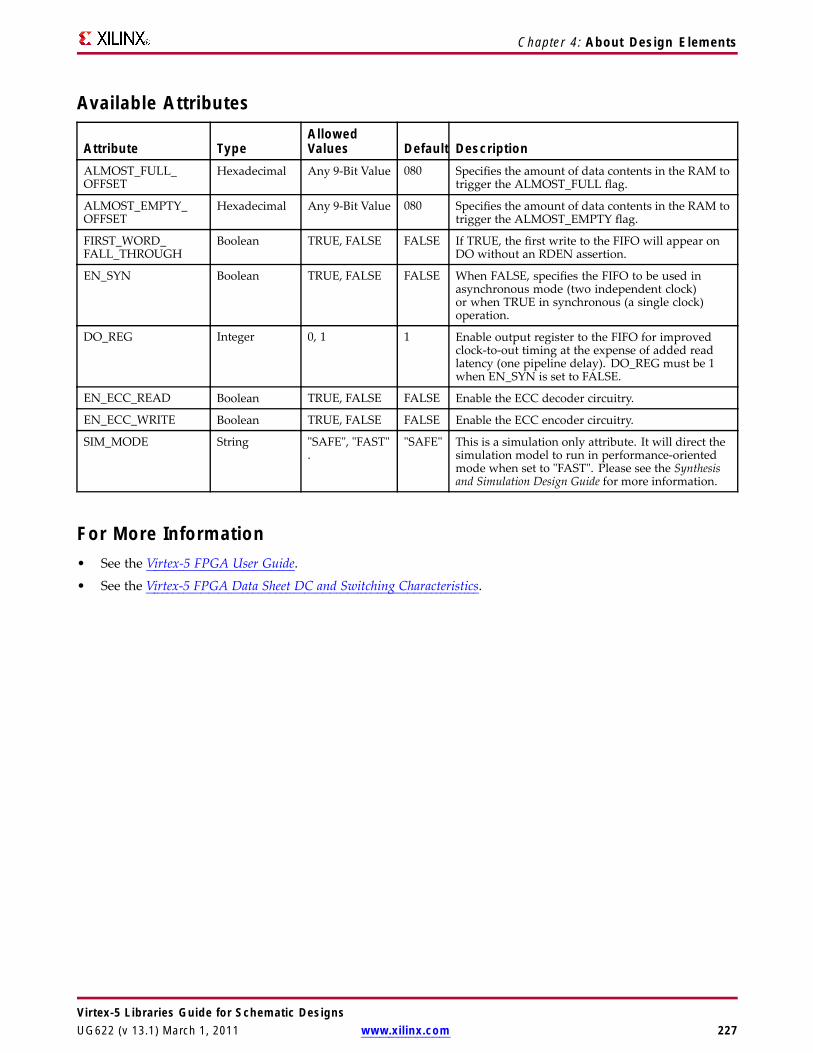
Chapter 4: About Design Elements
Available Attributes
Attribute TypeAllowedValues Default Description
ALMOST_FULL_OFFSET
Hexadecimal Any 9-Bit Value 080 Specifies the amount of data contents in the RAM totrigger the ALMOST_FULL flag.
ALMOST_EMPTY_OFFSET
Hexadecimal Any 9-Bit Value 080 Specifies the amount of data contents in the RAM totrigger the ALMOST_EMPTY flag.
FIRST_WORD_FALL_THROUGH
Boolean TRUE, FALSE FALSE If TRUE, the first write to the FIFO will appear onDO without an RDEN assertion.
EN_SYN Boolean TRUE, FALSE FALSE When FALSE, specifies the FIFO to be used inasynchronous mode (two independent clock)or when TRUE in synchronous (a single clock)operation.
DO_REG Integer 0, 1 1 Enable output register to the FIFO for improvedclock-to-out timing at the expense of added readlatency (one pipeline delay). DO_REG must be 1when EN_SYN is set to FALSE.
EN_ECC_READ Boolean TRUE, FALSE FALSE Enable the ECC decoder circuitry.
EN_ECC_WRITE Boolean TRUE, FALSE FALSE Enable the ECC encoder circuitry.
SIM_MODE String "SAFE", "FAST".
"SAFE" This is a simulation only attribute. It will direct thesimulation model to run in performance-orientedmode when set to "FAST". Please see the Synthesisand Simulation Design Guide for more information.
For More Information• See the Virtex-5 FPGA User Guide.
• See the Virtex-5 FPGA Data Sheet DC and Switching Characteristics.
Virtex-5 Libraries Guide for Schematic DesignsUG622 (v 13.1) March 1, 2011 www.xilinx.com 227

Chapter 4: About Design Elements
FJKCMacro: J-K Flip-Flop with Asynchronous Clear
IntroductionThis design element is a single J-K-type flip-flop with J, K, and asynchronous clear (CLR) inputs and data output(Q). The asynchronous clear (CLR) input, when High, overrides all other inputs and resets the Q output Low.When CLR is Low, the output responds to the state of the J and K inputs, as shown in the following logictable, during the Low-to-High clock (C) transition.
This flip-flop is asynchronously cleared, outputs Low, when power is applied. For FPGA devices, power-onconditions are simulated when global set/reset (GSR) is active. GSR defaults to active-High but can be invertedby adding an inverter in front of the GSR input of the appropriate STARTUP_architecture symbol.
Logic TableInputs Outputs
CLR J K C Q1 X X X 0
0 0 0 ↑ No Change
0 0 1 ↑ 0
0 1 0 ↑ 1
0 1 1 ↑ Toggle
Design Entry MethodThis design element is only for use in schematics.
Available Attributes
Attribute TypeAllowedValues Default Description
INIT Binary 0, 1 0 Sets the initial value of Q output after configuration
For Spartan®-6, the INIT value should always matchthe polarity of the set or reset. For this element, theINIT should be 0. If set to 1, an asynchronous circuitmust be created to exhibit this behavior, which Xilinxdoes not recommend.
Virtex-5 Libraries Guide for Schematic Designs228 www.xilinx.com UG622 (v 13.1) March 1, 2011

Chapter 4: About Design Elements
For More Information• See the Virtex-5 FPGA User Guide.
• See the Virtex-5 FPGA Data Sheet DC and Switching Characteristics.
Virtex-5 Libraries Guide for Schematic DesignsUG622 (v 13.1) March 1, 2011 www.xilinx.com 229
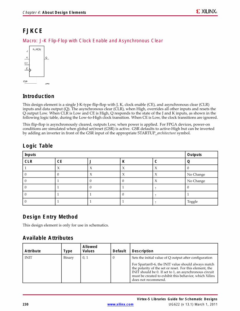
Chapter 4: About Design Elements
FJKCEMacro: J-K Flip-Flop with Clock Enable and Asynchronous Clear
IntroductionThis design element is a single J-K-type flip-flop with J, K, clock enable (CE), and asynchronous clear (CLR)inputs and data output (Q). The asynchronous clear (CLR), when High, overrides all other inputs and resets theQ output Low. When CLR is Low and CE is High, Q responds to the state of the J and K inputs, as shown in thefollowing logic table, during the Low-to-High clock transition. When CE is Low, the clock transitions are ignored.
This flip-flop is asynchronously cleared, outputs Low, when power is applied. For FPGA devices, power-onconditions are simulated when global set/reset (GSR) is active. GSR defaults to active-High but can be invertedby adding an inverter in front of the GSR input of the appropriate STARTUP_architecture symbol.
Logic TableInputs Outputs
CLR CE J K C Q1 X X X X 0
0 0 X X X No Change
0 1 0 0 X No Change
0 1 0 1 ↑ 0
0 1 1 0 ↑ 1
0 1 1 1 ↑ Toggle
Design Entry MethodThis design element is only for use in schematics.
Available Attributes
Attribute TypeAllowedValues Default Description
INIT Binary 0, 1 0 Sets the initial value of Q output after configuration
For Spartan®-6, the INIT value should always matchthe polarity of the set or reset. For this element, theINIT should be 0. If set to 1, an asynchronous circuitmust be created to exhibit this behavior, which Xilinxdoes not recommend.
Virtex-5 Libraries Guide for Schematic Designs230 www.xilinx.com UG622 (v 13.1) March 1, 2011

Chapter 4: About Design Elements
For More Information• See the Virtex-5 FPGA User Guide.
• See the Virtex-5 FPGA Data Sheet DC and Switching Characteristics.
Virtex-5 Libraries Guide for Schematic DesignsUG622 (v 13.1) March 1, 2011 www.xilinx.com 231

Chapter 4: About Design Elements
FJKPMacro: J-K Flip-Flop with Asynchronous Preset
IntroductionThis design element is a single J-K-type flip-flop with J, K, and asynchronous preset (PRE) inputs and dataoutput (Q). The asynchronous preset (PRE) input, when High, overrides all other inputs and sets the (Q) outputHigh. When (PRE) is Low, the (Q) output responds to the state of the J and K inputs, as shown in the followinglogic table, during the Low-to-High clock transition.
For FPGA devices, this flip-flop is asynchronously preset, output High, when power is applied. Power-onconditions are simulated when global set/reset (GSR) is active. GSR defaults to active-High but can be invertedby adding an inverter in front of the GSR input of the appropriate STARTUP_architecture symbol.
Logic TableInputs Outputs
PRE J K C Q1 X X X 1
0 0 0 X No Change
0 0 1 ↑ 0
0 1 0 ↑ 1
0 1 1 ↑ Toggle
Design Entry MethodThis design element is only for use in schematics.
Available Attributes
Attribute TypeAllowedValues Default Description
INIT Binary 0, 1 1 Sets the initial value of Q output after configuration
For Spartan®-6, Xilinx recommends that the INITvalue always matches the polarity of the set or reset.For this element, the INIT should be 1. If set to 0,additional asynchronous circuitry will be created tocorrectly model the behavior.
Virtex-5 Libraries Guide for Schematic Designs232 www.xilinx.com UG622 (v 13.1) March 1, 2011

Chapter 4: About Design Elements
For More Information• See the Virtex-5 FPGA User Guide.
• See the Virtex-5 FPGA Data Sheet DC and Switching Characteristics.
Virtex-5 Libraries Guide for Schematic DesignsUG622 (v 13.1) March 1, 2011 www.xilinx.com 233
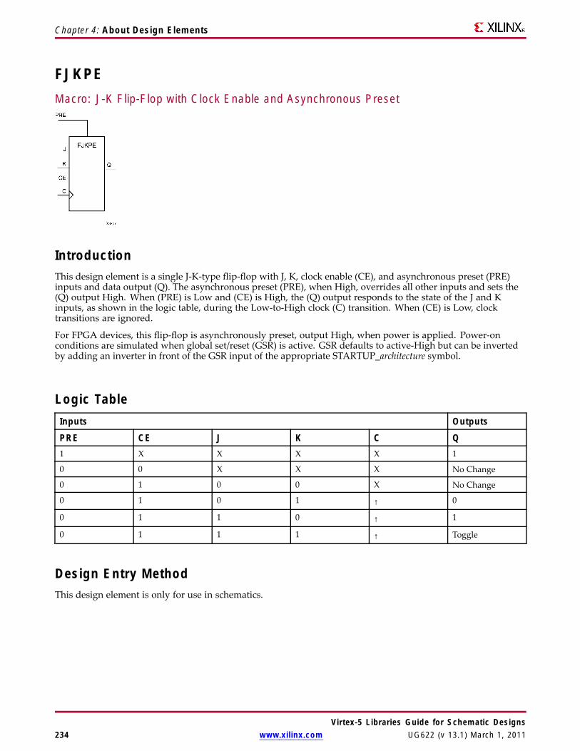
Chapter 4: About Design Elements
FJKPEMacro: J-K Flip-Flop with Clock Enable and Asynchronous Preset
IntroductionThis design element is a single J-K-type flip-flop with J, K, clock enable (CE), and asynchronous preset (PRE)inputs and data output (Q). The asynchronous preset (PRE), when High, overrides all other inputs and sets the(Q) output High. When (PRE) is Low and (CE) is High, the (Q) output responds to the state of the J and Kinputs, as shown in the logic table, during the Low-to-High clock (C) transition. When (CE) is Low, clocktransitions are ignored.
For FPGA devices, this flip-flop is asynchronously preset, output High, when power is applied. Power-onconditions are simulated when global set/reset (GSR) is active. GSR defaults to active-High but can be invertedby adding an inverter in front of the GSR input of the appropriate STARTUP_architecture symbol.
Logic TableInputs Outputs
PRE CE J K C Q1 X X X X 1
0 0 X X X No Change
0 1 0 0 X No Change
0 1 0 1 ↑ 0
0 1 1 0 ↑ 1
0 1 1 1 ↑ Toggle
Design Entry MethodThis design element is only for use in schematics.
Virtex-5 Libraries Guide for Schematic Designs234 www.xilinx.com UG622 (v 13.1) March 1, 2011
Chapter 4: About Design Elements
Available Attributes
Attribute TypeAllowedValues Default Description
INIT Binary 0, 1 1 Sets the initial value of Q output after configuration
For Spartan®-6, Xilinx recommends that the INITvalue always matches the polarity of the set or reset.For this element, the INIT should be 1. If set to 0,additional asynchronous circuitry will be created tocorrectly model the behavior.
For More Information• See the Virtex-5 FPGA User Guide.
• See the Virtex-5 FPGA Data Sheet DC and Switching Characteristics.
Virtex-5 Libraries Guide for Schematic DesignsUG622 (v 13.1) March 1, 2011 www.xilinx.com 235

Chapter 4: About Design Elements
FJKRSEMacro: J-K Flip-Flop with Clock Enable and Synchronous Reset and Set
IntroductionThis design element is a single J-K-type flip-flop with J, K, synchronous reset (R), synchronous set (S), and clockenable (CE) inputs and data output (Q). When synchronous reset (R) is High during the Low-to-High clock (C)transition, all other inputs are ignored and output (Q) is reset Low. When synchronous set (S) is High and (R) isLow, output (Q) is set High. When (R) and (S) are Low and (CE) is High, output (Q) responds to the state ofthe J and K inputs, according to the following logic table, during the Low-to-High clock (C) transition. When(CE) is Low, clock transitions are ignored.
This flip-flop is asynchronously cleared, outputs Low, when power is applied. For FPGA devices, power-onconditions are simulated when global set/reset (GSR) is active. GSR defaults to active-High but can be invertedby adding an inverter in front of the GSR input of the appropriate STARTUP_architecture symbol.
Logic TableInputs Outputs
R S CE J K C Q1 X X X X ↑ 0
0 1 X X X ↑ 1
0 0 0 X X X No Change
0 0 1 0 0 X No Change
0 0 1 0 1 ↑ 0
0 0 1 1 0 ↑ 1
0 0 1 1 0 ↑ 1
0 0 1 1 1 ↑ Toggle
Design Entry MethodThis design element is only for use in schematics.
Available Attributes
Attribute TypeAllowedValues Default Description
INIT Binary 0, 1 0 Sets the initial value of Q output after configuration
Virtex-5 Libraries Guide for Schematic Designs236 www.xilinx.com UG622 (v 13.1) March 1, 2011

Chapter 4: About Design Elements
For More Information• See the Virtex-5 FPGA User Guide.
• See the Virtex-5 FPGA Data Sheet DC and Switching Characteristics.
Virtex-5 Libraries Guide for Schematic DesignsUG622 (v 13.1) March 1, 2011 www.xilinx.com 237

Chapter 4: About Design Elements
FJKSREMacro: J-K Flip-Flop with Clock Enable and Synchronous Set and Reset
IntroductionThis design element is a single J-K-type flip-flop with J, K, synchronous set (S), synchronous reset (R), and clockenable (CE) inputs and data output (Q). When synchronous set (S) is High during the Low-to-High clock (C)transition, all other inputs are ignored and output (Q) is set High. When synchronous reset (R) is High and (S) isLow, output (Q) is reset Low. When (S) and (R) are Low and (CE) is High, output (Q) responds to the state ofthe J and K inputs, as shown in the following logic table, during the Low-to-High clock (C) transition. When(CE) is Low, clock transitions are ignored.
This flip-flop is asynchronously cleared, outputs Low, when power is applied. For FPGA devices, power-onconditions are simulated when global set/reset (GSR) is active. GSR defaults to active-High but can be invertedby adding an inverter in front of the GSR input of the appropriate STARTUP_architecture symbol.
Logic TableInputs Outputs
S R CE J K C Q1 X X X X ↑ 1
0 1 X X X ↑ 0
0 0 0 X X X No Change
0 0 1 0 0 X No Change
0 0 1 0 1 ↑ 0
0 0 1 1 0 ↑ 1
0 0 1 1 1 ↑ Toggle
Design Entry MethodThis design element is only for use in schematics.
Available Attributes
Attribute TypeAllowedValues Default Description
INIT Binary 0, 1 1 Sets the initial value of Q output after configuration.
Virtex-5 Libraries Guide for Schematic Designs238 www.xilinx.com UG622 (v 13.1) March 1, 2011

Chapter 4: About Design Elements
For More Information• See the Virtex-5 FPGA User Guide.
• See the Virtex-5 FPGA Data Sheet DC and Switching Characteristics.
Virtex-5 Libraries Guide for Schematic DesignsUG622 (v 13.1) March 1, 2011 www.xilinx.com 239

Chapter 4: About Design Elements
FRAME_ECC_VIRTEX5Primitive: Virtex®-5 Configuration Frame Error Detection and Correction Circuitry
IntroductionThis design element enables the dedicated, built-in ECC (Error Detection and Correction Circuitry) for theconfiguration memory of the FPGA. This element contains outputs that allow monitoring of the status of the ECCcircuitry and the status of the readback CRC circuitry.
Port DescriptionsPort Direction Width FunctionECCERROR Output 1 Frame ECC error found. Value is a one when SYNDROME is non-zero
and a zero when SYNDROME is all zeroes indicating no errors detected.
SYNDROME Output 12 Frame ECC error where:
• No errors: All zeros.
• One bit error: SYNDROME[11]=0, SYNDROME[10:0]= location oferror in FRAME.
• Two bit errors: SYNDROME[11]=1, SYNDROME[10:0]=don’t care.
• More than two bit errors: Unknown output.
SYNDROMEVALID Output 1 Frame ECC output indicating that the value on SYNDROME is valid.
CRCERROR Output 1 Readback CRC error.
Design Entry MethodThis design element can be used in schematics.
For More Information• See the Virtex-5 FPGA User Guide.
• See the Virtex-5 FPGA Data Sheet DC and Switching Characteristics.
Virtex-5 Libraries Guide for Schematic Designs240 www.xilinx.com UG622 (v 13.1) March 1, 2011

Chapter 4: About Design Elements
FTCMacro: Toggle Flip-Flop with Asynchronous Clear
IntroductionThis design element is a synchronous, resettable toggle flip-flop. The asynchronous clear (CLR) input, whenHigh, overrides all other inputs and resets the data output (Q) Low. The (Q) output toggles, or changes state,when the toggle enable (T) input is High and (CLR) is Low during the Low-to-High clock transition.
This flip-flop is asynchronously cleared, outputs Low, when power is applied. For FPGA devices, power-onconditions are simulated when global set/reset (GSR) is active. GSR defaults to active-High but can be invertedby adding an inverter in front of the GSR input of the appropriate STARTUP_architecture symbol.
Logic TableInputs Outputs
CLR T C Q1 X X 0
0 0 X No Change
0 1 ↑ Toggle
Design Entry MethodYou can instantiate this element when targeting a CPLD, but not when you are targeting an FPGA.
Available Attributes
Attribute TypeAllowedValues Default Description
INIT Binary 0, 1 0 Sets the initial value of Q output after configuration
For Spartan®-6, the INIT value should always matchthe polarity of the set or reset. For this element, theINIT should be 0. If set to 1, an asynchronous circuitmust be created to exhibit this behavior, which Xilinxdoes not recommend.
For More Information• See the Virtex-5 FPGA User Guide.• See the Virtex-5 FPGA Data Sheet DC and Switching Characteristics.
Virtex-5 Libraries Guide for Schematic DesignsUG622 (v 13.1) March 1, 2011 www.xilinx.com 241

Chapter 4: About Design Elements
FTCEMacro: Toggle Flip-Flop with Clock Enable and Asynchronous Clear
IntroductionThis design element is a toggle flip-flop with toggle and clock enable and asynchronous clear. When theasynchronous clear (CLR) input is High, all other inputs are ignored and the data output (Q) is reset Low. WhenCLR is Low and toggle enable (T) and clock enable (CE) are High, Q output toggles, or changes state, during theLow-to-High clock (C) transition. When CE is Low, clock transitions are ignored.
This flip-flop is asynchronously cleared, outputs Low, when power is applied. For FPGA devices, power-onconditions are simulated when global set/reset (GSR) is active. GSR defaults to active-High but can be invertedby adding an inverter in front of the GSR input of the appropriate STARTUP_architecture symbol.
Logic TableInputs Outputs
CLR CE T C Q1 X X X 0
0 0 X X No Change
0 1 0 X No Change
0 1 1 ↑ Toggle
Design Entry MethodThis design element is only for use in schematics.
Available Attributes
Attribute TypeAllowedValues Default Description
INIT Binary 0, 1 0 Sets the initial value of Q output after configuration
For Spartan®-6, the INIT value should always matchthe polarity of the set or reset. For this element, theINIT should be 0. If set to 1, an asynchronous circuitmust be created to exhibit this behavior, which Xilinxdoes not recommend.
For More Information• See the Virtex-5 FPGA User Guide.• See the Virtex-5 FPGA Data Sheet DC and Switching Characteristics.
Virtex-5 Libraries Guide for Schematic Designs242 www.xilinx.com UG622 (v 13.1) March 1, 2011

Chapter 4: About Design Elements
FTCLEMacro: Toggle/Loadable Flip-Flop with Clock Enable and Asynchronous Clear
IntroductionThis design element is a toggle/loadable flip-flop with toggle and clock enable and asynchronous clear. Whenthe asynchronous clear input (CLR) is High, all other inputs are ignored and output Q is reset Low. When loadenable input (L) is High and CLR is Low, clock enable (CE) is overridden and the data on data input (D) isloaded into the flip-flop during the Low-to-High clock (C) transition. When toggle enable (T) and CE are Highand L and CLR are Low, output Q toggles, or changes state, during the Low- to-High clock transition. WhenCE is Low, clock transitions are ignored.
This flip-flop is asynchronously cleared, outputs Low, when power is applied. For FPGA devices, power-onconditions are simulated when global set/reset (GSR) is active. GSR defaults to active-High but can be invertedby adding an inverter in front of the GSR input of the appropriate STARTUP_architecture symbol.
Logic TableInputs Outputs
CLR L CE T D C Q1 X X X X X 0
0 1 X X D ↑ D
0 0 0 X X X No Change
0 0 1 0 X X No Change
0 0 1 1 X ↑ Toggle
Design Entry MethodThis design element is only for use in schematics.
Available Attributes
Attribute TypeAllowedValues Default Description
INIT Binary 0, 1 0 Sets the initial value of Q output after configuration
For Spartan®-6, the INIT value should always matchthe polarity of the set or reset. For this element, theINIT should be 0. If set to 1, an asynchronous circuitmust be created to exhibit this behavior, which Xilinxdoes not recommend.
Virtex-5 Libraries Guide for Schematic DesignsUG622 (v 13.1) March 1, 2011 www.xilinx.com 243

Chapter 4: About Design Elements
For More Information• See the Virtex-5 FPGA User Guide.
• See the Virtex-5 FPGA Data Sheet DC and Switching Characteristics.
Virtex-5 Libraries Guide for Schematic Designs244 www.xilinx.com UG622 (v 13.1) March 1, 2011

Chapter 4: About Design Elements
FTCLEXMacro: Toggle/Loadable Flip-Flop with Clock Enable and Asynchronous Clear
IntroductionThis design element is a toggle/loadable flip-flop with toggle and clock enable and asynchronous clear. Whenthe asynchronous clear input (CLR) is High, all other inputs are ignored and output Q is reset Low. When loadenable input (L) is High, CLR is Low, and CE is High, the data on data input (D) is loaded into the flip-flop duringthe Low-to-High clock (C) transition. When toggle enable (T) and CE are High and L and CLR are Low, output Qtoggles, or changes state, during the Low- to-High clock transition. When CE is Low, clock transitions are ignored.
This flip-flop is asynchronously cleared, outputs Low, when power is applied. For FPGA devices, power-onconditions are simulated when global set/reset (GSR) is active. GSR defaults to active-High but can be invertedby adding an inverter in front of the GSR input of the appropriate STARTUP_architecture symbol.
Logic TableInputs Outputs
CLR L CE T D C Q1 X X X X X 0
0 1 X X D ↑ D
0 0 0 X X X No Change
0 0 1 0 X X No Change
0 0 1 1 X ↑ Toggle
Design Entry MethodThis design element is only for use in schematics.
Available Attributes
Attribute TypeAllowedValues Default Description
INIT Binary 0, 1 0 Sets the initial value of Q output after configuration
For Spartan®-6, the INIT value should always matchthe polarity of the set or reset. For this element, theINIT should be 0. If set to 1, an asynchronous circuitmust be created to exhibit this behavior, which Xilinxdoes not recommend.
Virtex-5 Libraries Guide for Schematic DesignsUG622 (v 13.1) March 1, 2011 www.xilinx.com 245

Chapter 4: About Design Elements
For More Information• See the Virtex-5 FPGA User Guide.
• See the Virtex-5 FPGA Data Sheet DC and Switching Characteristics.
Virtex-5 Libraries Guide for Schematic Designs246 www.xilinx.com UG622 (v 13.1) March 1, 2011

Chapter 4: About Design Elements
FTPMacro: Toggle Flip-Flop with Asynchronous Preset
IntroductionThis design element is a toggle flip-flop with toggle enable and asynchronous preset. When the asynchronouspreset (PRE) input is High, all other inputs are ignored and output (Q) is set High. When toggle-enable input (T)is High and (PRE) is Low, output (Q) toggles, or changes state, during the Low-to-High clock (C) transition.
For FPGA devices, this flip-flop is asynchronously preset, output High, when power is applied. Power-onconditions are simulated when global set/reset (GSR) is active. GSR defaults to active-High but can be invertedby adding an inverter in front of the GSR input of the appropriate STARTUP_architecture symbol.
Logic TableInputs Outputs
PRE T C Q1 X X 1
0 0 X No Change
0 1 ↑ Toggle
Design Entry MethodThis design element is only for use in schematics.
Available Attributes
Attribute TypeAllowedValues Default Description
INIT Binary 0, 1 1 Sets the initial value of Q output after configuration
For Spartan®-6, Xilinx recommends that the INITvalue always matches the polarity of the set or reset.For this element, the INIT should be 1. If set to 0,additional asynchronous circuitry will be created tocorrectly model the behavior.
For More Information• See the Virtex-5 FPGA User Guide.• See the Virtex-5 FPGA Data Sheet DC and Switching Characteristics.
Virtex-5 Libraries Guide for Schematic DesignsUG622 (v 13.1) March 1, 2011 www.xilinx.com 247
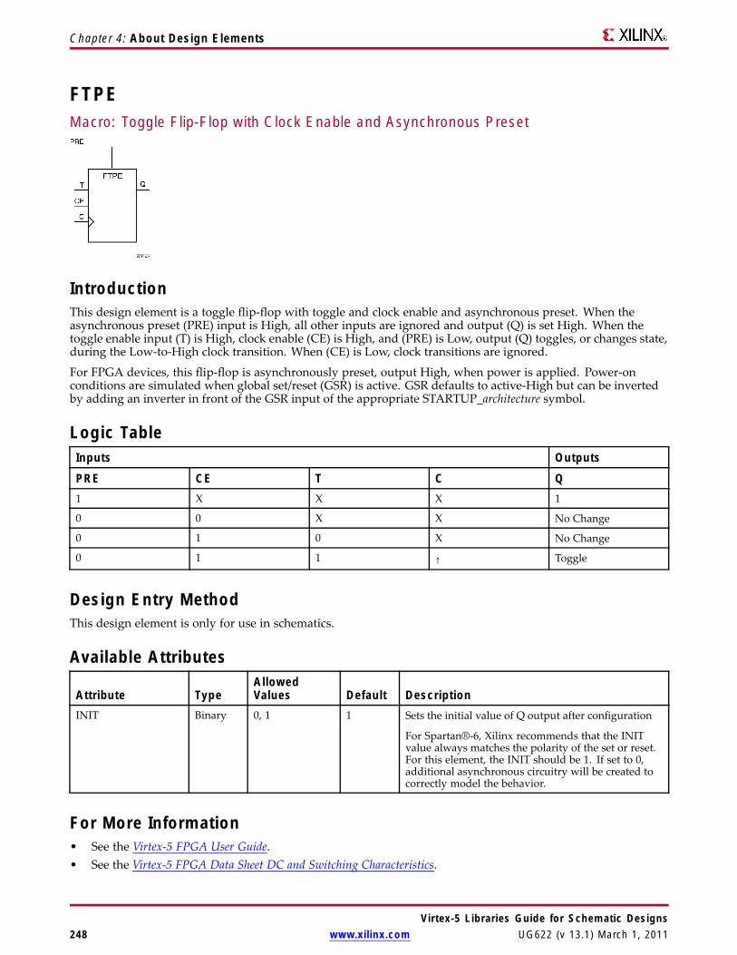
Chapter 4: About Design Elements
FTPEMacro: Toggle Flip-Flop with Clock Enable and Asynchronous Preset
IntroductionThis design element is a toggle flip-flop with toggle and clock enable and asynchronous preset. When theasynchronous preset (PRE) input is High, all other inputs are ignored and output (Q) is set High. When thetoggle enable input (T) is High, clock enable (CE) is High, and (PRE) is Low, output (Q) toggles, or changes state,during the Low-to-High clock transition. When (CE) is Low, clock transitions are ignored.
For FPGA devices, this flip-flop is asynchronously preset, output High, when power is applied. Power-onconditions are simulated when global set/reset (GSR) is active. GSR defaults to active-High but can be invertedby adding an inverter in front of the GSR input of the appropriate STARTUP_architecture symbol.
Logic TableInputs Outputs
PRE CE T C Q1 X X X 1
0 0 X X No Change
0 1 0 X No Change
0 1 1 ↑ Toggle
Design Entry MethodThis design element is only for use in schematics.
Available Attributes
Attribute TypeAllowedValues Default Description
INIT Binary 0, 1 1 Sets the initial value of Q output after configuration
For Spartan®-6, Xilinx recommends that the INITvalue always matches the polarity of the set or reset.For this element, the INIT should be 1. If set to 0,additional asynchronous circuitry will be created tocorrectly model the behavior.
For More Information• See the Virtex-5 FPGA User Guide.• See the Virtex-5 FPGA Data Sheet DC and Switching Characteristics.
Virtex-5 Libraries Guide for Schematic Designs248 www.xilinx.com UG622 (v 13.1) March 1, 2011

Chapter 4: About Design Elements
FTPLEMacro: Toggle/Loadable Flip-Flop with Clock Enable and Asynchronous Preset
IntroductionThis design element is a toggle/loadable flip-flop with toggle and clock enable and asynchronous preset. Whenthe asynchronous preset input (PRE) is High, all other inputs are ignored and output (Q) is set High. When theload enable input (L) is High and (PRE) is Low, the clock enable (CE) is overridden and the data (D) is loadedinto the flip-flop during the Low-to-High clock transition. When L and PRE are Low and toggle-enable input(T) and (CE) are High, output (Q) toggles, or changes state, during the Low-to-High clock transition. When(CE) is Low, clock transitions are ignored.
For FPGA devices, this flip-flop is asynchronously preset, output High, when power is applied. Power-onconditions are simulated when global set/reset (GSR) is active. GSR defaults to active-High but can be invertedby adding an inverter in front of the GSR input of the appropriate STARTUP_architecture symbol.
Logic TableInputs Outputs
PRE L CE T D C Q1 X X X X X 1
0 1 X X D ↑ D
0 0 0 X X X No Change
0 0 1 0 X X No Change
0 0 1 1 X ↑ Toggle
Design Entry MethodThis design element is only for use in schematics.
Virtex-5 Libraries Guide for Schematic DesignsUG622 (v 13.1) March 1, 2011 www.xilinx.com 249
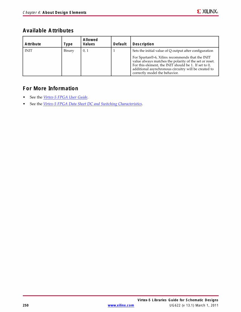
Chapter 4: About Design Elements
Available Attributes
Attribute TypeAllowedValues Default Description
INIT Binary 0, 1 1 Sets the initial value of Q output after configuration
For Spartan®-6, Xilinx recommends that the INITvalue always matches the polarity of the set or reset.For this element, the INIT should be 1. If set to 0,additional asynchronous circuitry will be created tocorrectly model the behavior.
For More Information• See the Virtex-5 FPGA User Guide.
• See the Virtex-5 FPGA Data Sheet DC and Switching Characteristics.
Virtex-5 Libraries Guide for Schematic Designs250 www.xilinx.com UG622 (v 13.1) March 1, 2011
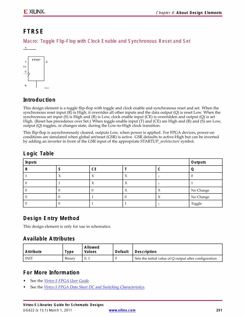
Chapter 4: About Design Elements
FTRSEMacro: Toggle Flip-Flop with Clock Enable and Synchronous Reset and Set
IntroductionThis design element is a toggle flip-flop with toggle and clock enable and synchronous reset and set. When thesynchronous reset input (R) is High, it overrides all other inputs and the data output (Q) is reset Low. When thesynchronous set input (S) is High and (R) is Low, clock enable input (CE) is overridden and output (Q) is setHigh. (Reset has precedence over Set.) When toggle enable input (T) and (CE) are High and (R) and (S) are Low,output (Q) toggles, or changes state, during the Low-to-High clock transition.
This flip-flop is asynchronously cleared, outputs Low, when power is applied. For FPGA devices, power-onconditions are simulated when global set/reset (GSR) is active. GSR defaults to active-High but can be invertedby adding an inverter in front of the GSR input of the appropriate STARTUP_architecture symbol.
Logic TableInputs Outputs
R S CE T C Q1 X X X ↑ 0
0 1 X X ↑ 1
0 0 0 X X No Change
0 0 1 0 X No Change
0 0 1 1 ↑ Toggle
Design Entry MethodThis design element is only for use in schematics.
Available Attributes
Attribute TypeAllowedValues Default Description
INIT Binary 0, 1 0 Sets the initial value of Q output after configuration
For More Information• See the Virtex-5 FPGA User Guide.• See the Virtex-5 FPGA Data Sheet DC and Switching Characteristics.
Virtex-5 Libraries Guide for Schematic DesignsUG622 (v 13.1) March 1, 2011 www.xilinx.com 251

Chapter 4: About Design Elements
FTRSLEMacro: Toggle/Loadable Flip-Flop with Clock Enable and Synchronous Reset and Set
IntroductionThis design element is a toggle/loadable flip-flop with toggle and clock enable and synchronous reset and set.The synchronous reset input (R), when High, overrides all other inputs and resets the data output (Q) Low.(Reset has precedence over Set.) When R is Low and synchronous set input (S) is High, the clock enable input(CE) is overridden and output Q is set High. When R and S are Low and load enable input (L) is High, CE isoverridden and data on data input (D) is loaded into the flip-flop during the Low-to-High clock transition. WhenR, S, and L are Low, CE is High and T is High, output Q toggles, or changes state, during the Low-to-High clocktransition. When CE is Low, clock transitions are ignored.
This flip-flop is asynchronously cleared, outputs Low, when power is applied. For FPGA devices, power-onconditions are simulated when global set/reset (GSR) is active. GSR defaults to active-High but can be invertedby adding an inverter in front of the GSR input of the appropriate STARTUP_architecture symbol.
Logic TableInputs Outputs
R S L CE T D C Q1 0 X X X X ↑ 0
0 1 X X X X ↑ 1
0 0 1 X X 1 ↑ 1
0 0 1 X X 0 ↑ 0
0 0 0 0 X X X No Change
0 0 0 1 0 X X No Change
0 0 0 1 1 X ↑ Toggle
Design Entry MethodThis design element is only for use in schematics.
Virtex-5 Libraries Guide for Schematic Designs252 www.xilinx.com UG622 (v 13.1) March 1, 2011

Chapter 4: About Design Elements
Available Attributes
Attribute TypeAllowedValues Default Description
INIT Binary 0, 1 0 Sets the initial value of Q output after configuration
For More Information• See the Virtex-5 FPGA User Guide.
• See the Virtex-5 FPGA Data Sheet DC and Switching Characteristics.
Virtex-5 Libraries Guide for Schematic DesignsUG622 (v 13.1) March 1, 2011 www.xilinx.com 253
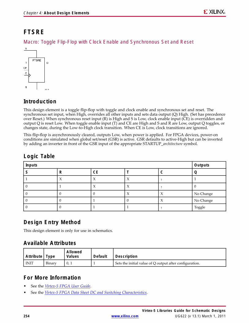
Chapter 4: About Design Elements
FTSREMacro: Toggle Flip-Flop with Clock Enable and Synchronous Set and Reset
IntroductionThis design element is a toggle flip-flop with toggle and clock enable and synchronous set and reset. Thesynchronous set input, when High, overrides all other inputs and sets data output (Q) High. (Set has precedenceover Reset.) When synchronous reset input (R) is High and S is Low, clock enable input (CE) is overridden andoutput Q is reset Low. When toggle enable input (T) and CE are High and S and R are Low, output Q toggles, orchanges state, during the Low-to-High clock transition. When CE is Low, clock transitions are ignored.
This flip-flop is asynchronously cleared, outputs Low, when power is applied. For FPGA devices, power-onconditions are simulated when global set/reset (GSR) is active. GSR defaults to active-High but can be invertedby adding an inverter in front of the GSR input of the appropriate STARTUP_architecture symbol.
Logic TableInputs Outputs
S R CE T C Q1 X X X ↑ 1
0 1 X X ↑ 0
0 0 0 X X No Change
0 0 1 0 X No Change
0 0 1 1 ↑ Toggle
Design Entry MethodThis design element is only for use in schematics.
Available Attributes
Attribute TypeAllowedValues Default Description
INIT Binary 0, 1 1 Sets the initial value of Q output after configuration.
For More Information• See the Virtex-5 FPGA User Guide.• See the Virtex-5 FPGA Data Sheet DC and Switching Characteristics.
Virtex-5 Libraries Guide for Schematic Designs254 www.xilinx.com UG622 (v 13.1) March 1, 2011

Chapter 4: About Design Elements
FTSRLEMacro: Toggle/Loadable Flip-Flop with Clock Enable and Synchronous Set and Reset
IntroductionThis design element is a toggle/loadable flip-flop with toggle and clock enable and synchronous set and reset.The synchronous set input (S), when High, overrides all other inputs and sets data output (Q) High. (Set hasprecedence over Reset.) When synchronous reset (R) is High and (S) is Low, clock enable input (CE) is overriddenand output (Q) is reset Low. When load enable input (L) is High and S and R are Low, CE is overridden and dataon data input (D) is loaded into the flip-flop during the Low-to-High clock transition. When the toggle enableinput (T) and (CE) are High and (S), (R), and (L) are Low, output (Q) toggles, or changes state, during the Low-to-High clock transition. When (CE) is Low, clock transitions are ignored.
For FPGA devices, power-on conditions are simulated when global set/reset (GSR) is active. GSR defaultsto active-High but can be inverted by adding an inverter in front of the GSR input of the appropriateSTARTUP_architecture symbol.
Logic TableInputs Outputs
S R L CE T D C Q1 X X X X X ↑ 1
0 1 X X X X ↑ 0
0 0 1 X X 1 ↑ 1
0 0 1 X X 0 ↑ 0
0 0 0 0 X X X No Change
0 0 0 1 0 X X No Change
0 0 0 1 1 X ↑ Toggle
Design Entry MethodThis design element is only for use in schematics.
Virtex-5 Libraries Guide for Schematic DesignsUG622 (v 13.1) March 1, 2011 www.xilinx.com 255

Chapter 4: About Design Elements
Available Attributes
Attribute TypeAllowedValues Default Description
INIT Binary 0, 1 1 Sets the initial value of Q output after configuration.
For More Information• See the Virtex-5 FPGA User Guide.
• See the Virtex-5 FPGA Data Sheet DC and Switching Characteristics.
Virtex-5 Libraries Guide for Schematic Designs256 www.xilinx.com UG622 (v 13.1) March 1, 2011

Chapter 4: About Design Elements
GNDPrimitive: Ground-Connection Signal Tag
IntroductionThe GND signal tag, or parameter, forces a net or input function to a Low logic level. A net tied to GND cannothave any other source.
When the logic-trimming software or fitter encounters a net or input function tied to GND, it removes any logicthat is disabled by the GND signal. The GND signal is only implemented when the disabled logic cannotbe removed.
Design Entry MethodThis design element is only for use in schematics.
For More Information• See the Virtex-5 FPGA User Guide.
• See the Virtex-5 FPGA Data Sheet DC and Switching Characteristics.
Virtex-5 Libraries Guide for Schematic DesignsUG622 (v 13.1) March 1, 2011 www.xilinx.com 257
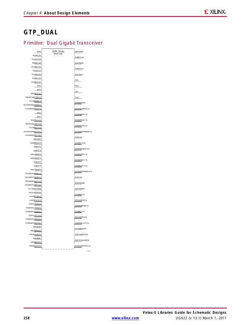
Chapter 4: About Design Elements
GTP_DUALPrimitive: Dual Gigabit Transceiver
Virtex-5 Libraries Guide for Schematic Designs258 www.xilinx.com UG622 (v 13.1) March 1, 2011

Chapter 4: About Design Elements
IntroductionThis design element is a power-efficient transceiver for Virtex®-5 FPGAs. The GTP transceiver is highlyconfigurable and tightly integrated with the programmable logic resources of the FPGA.
Virtex-5 Libraries Guide for Schematic DesignsUG622 (v 13.1) March 1, 2011 www.xilinx.com 259
Chapter 4: About Design Elements
Design Entry Method
For More Information• See the Virtex-5 FPGA RocketIO GTP Transceivers User Guide.
• See the Virtex-5 FPGA Data Sheet DC and Switching Characteristics.
• See the Virtex-5 FPGA User Guide.
Virtex-5 Libraries Guide for Schematic Designs260 www.xilinx.com UG622 (v 13.1) March 1, 2011
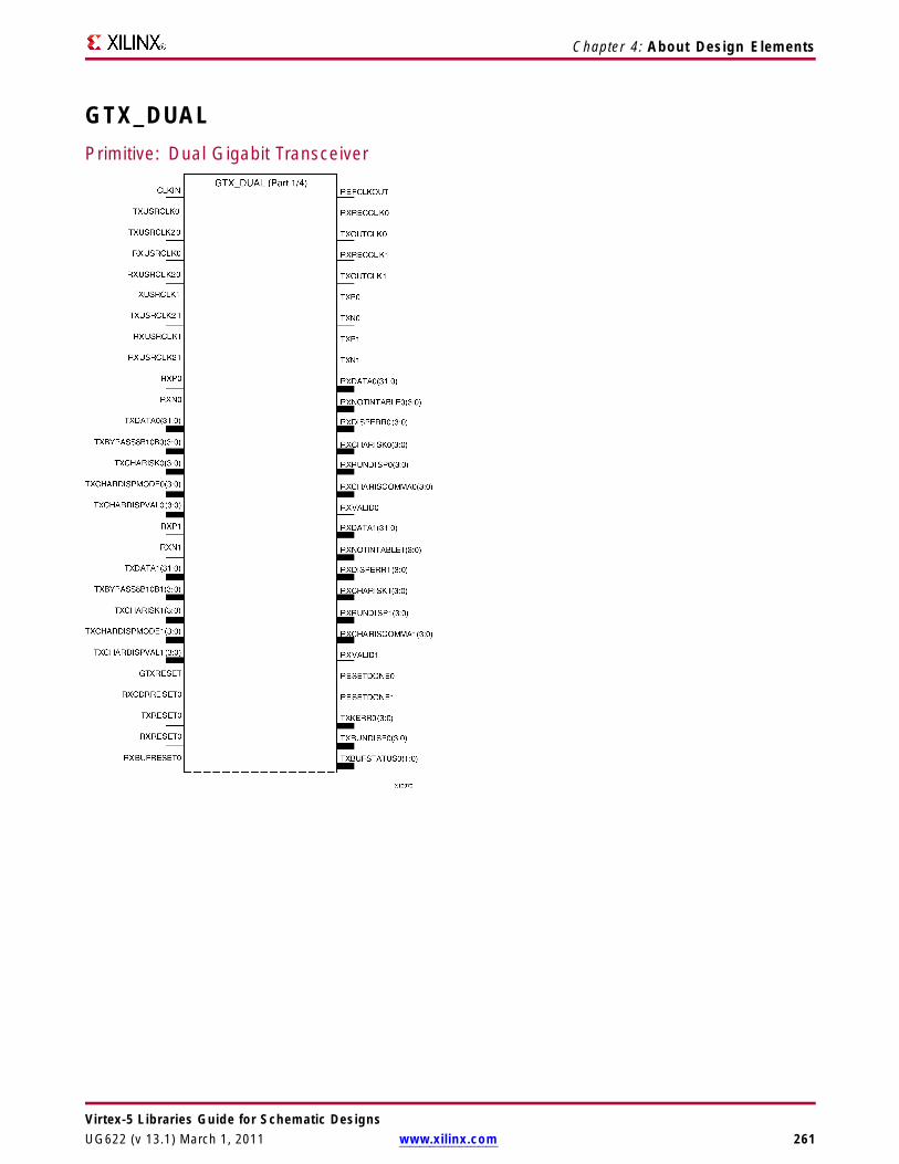
Chapter 4: About Design Elements
GTX_DUALPrimitive: Dual Gigabit Transceiver
Virtex-5 Libraries Guide for Schematic DesignsUG622 (v 13.1) March 1, 2011 www.xilinx.com 261

Chapter 4: About Design Elements
Virtex-5 Libraries Guide for Schematic Designs262 www.xilinx.com UG622 (v 13.1) March 1, 2011
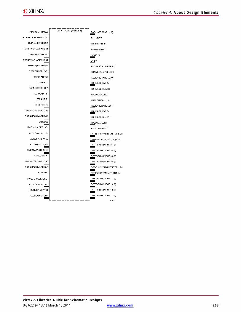
Chapter 4: About Design Elements
Virtex-5 Libraries Guide for Schematic DesignsUG622 (v 13.1) March 1, 2011 www.xilinx.com 263
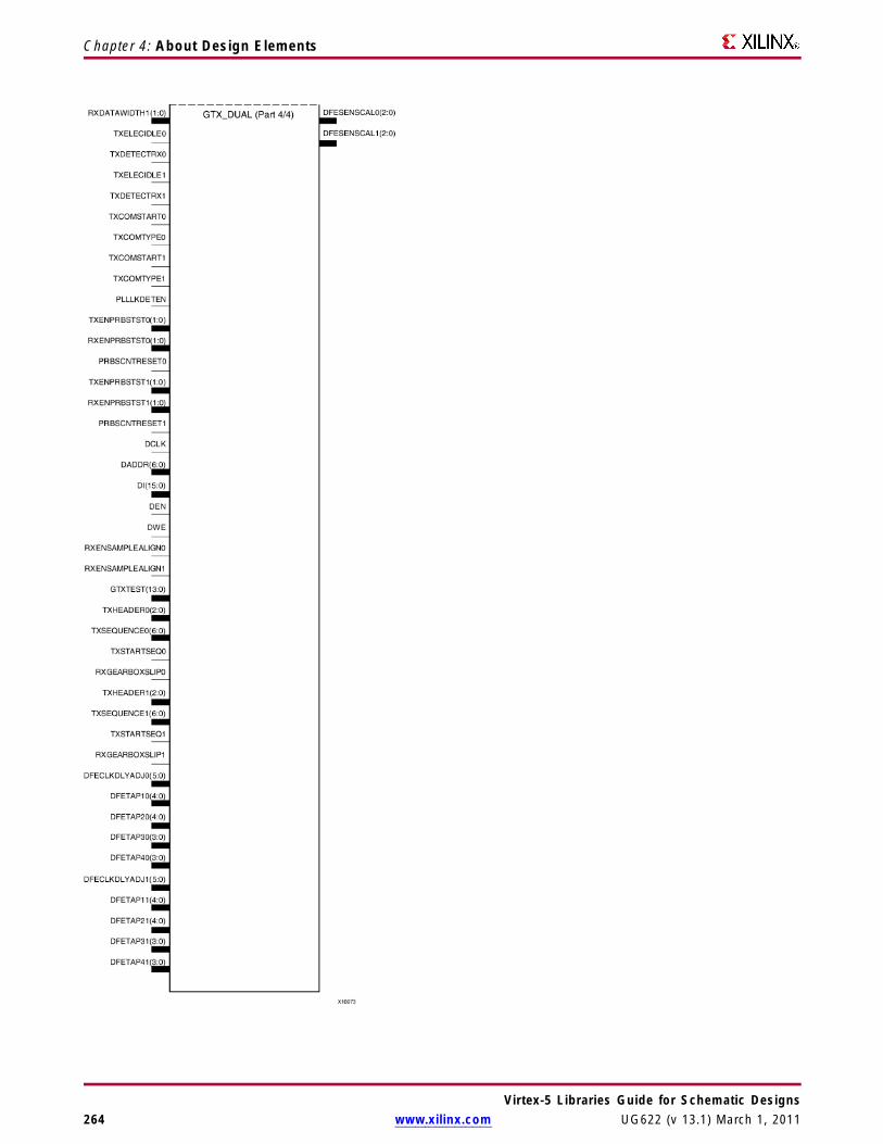
Chapter 4: About Design Elements
Virtex-5 Libraries Guide for Schematic Designs264 www.xilinx.com UG622 (v 13.1) March 1, 2011
Chapter 4: About Design Elements
IntroductionThis design element is a power-efficient transceiver for Virtex®-5 FPGAs. The GTX transceiver is highlyconfigurable and tightly integrated with the programmable logic resources of the FPGA.
Design Entry Method
For More Information• See the Virtex-5 FPGA RocketIO GTX Transceivers User Guide.
• See the Virtex-5 FPGA Data Sheet DC and Switching Characteristics.
• See the Virtex-5 FPGA User Guide.
Virtex-5 Libraries Guide for Schematic DesignsUG622 (v 13.1) March 1, 2011 www.xilinx.com 265
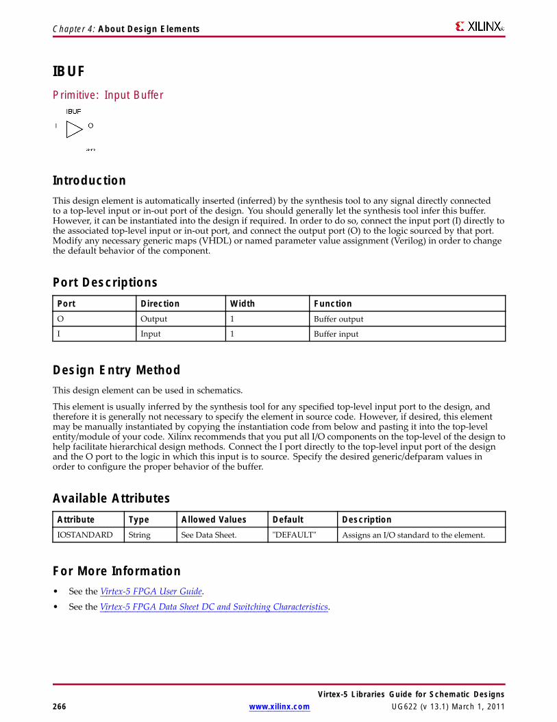
Chapter 4: About Design Elements
IBUFPrimitive: Input Buffer
IntroductionThis design element is automatically inserted (inferred) by the synthesis tool to any signal directly connectedto a top-level input or in-out port of the design. You should generally let the synthesis tool infer this buffer.However, it can be instantiated into the design if required. In order to do so, connect the input port (I) directly tothe associated top-level input or in-out port, and connect the output port (O) to the logic sourced by that port.Modify any necessary generic maps (VHDL) or named parameter value assignment (Verilog) in order to changethe default behavior of the component.
Port DescriptionsPort Direction Width FunctionO Output 1 Buffer output
I Input 1 Buffer input
Design Entry MethodThis design element can be used in schematics.
This element is usually inferred by the synthesis tool for any specified top-level input port to the design, andtherefore it is generally not necessary to specify the element in source code. However, if desired, this elementmay be manually instantiated by copying the instantiation code from below and pasting it into the top-levelentity/module of your code. Xilinx recommends that you put all I/O components on the top-level of the design tohelp facilitate hierarchical design methods. Connect the I port directly to the top-level input port of the designand the O port to the logic in which this input is to source. Specify the desired generic/defparam values inorder to configure the proper behavior of the buffer.
Available AttributesAttribute Type Allowed Values Default DescriptionIOSTANDARD String See Data Sheet. "DEFAULT" Assigns an I/O standard to the element.
For More Information• See the Virtex-5 FPGA User Guide.
• See the Virtex-5 FPGA Data Sheet DC and Switching Characteristics.
Virtex-5 Libraries Guide for Schematic Designs266 www.xilinx.com UG622 (v 13.1) March 1, 2011

Chapter 4: About Design Elements
IBUF16Macro: 16-Bit Input Buffer
IntroductionInput Buffers isolate the internal circuit from the signals coming into the chip. This design element is containedin input/output blocks (IOBs) and allows the specification of the particular I/O Standard to configure the I/O. Ingeneral, an this element should be used for all single-ended data input or bidirectional pins.
Design Entry MethodThis design element can be used in schematics.
This element is usually inferred by the synthesis tool for any specified top-level input port to the design, andtherefore it is generally not necessary to specify the element in source code. However, if desired, this elementmay be manually instantiated by copying the instantiation code from below and pasting it into the top-levelentity/module of your code. Xilinx recommends that you put all I/O components on the top-level of the design tohelp facilitate hierarchical design methods. Connect the I port directly to the top-level input port of the designand the O port to the logic in which this input is to source. Specify the desired generic/defparam values inorder to configure the proper behavior of the buffer.
Available AttributesAttribute Type Allowed Values Default DescriptionIOSTANDARD String See Data Sheet. "DEFAULT" Assigns an I/O standard to the element.
For More Information• See the Virtex-5 FPGA User Guide.
• See the Virtex-5 FPGA Data Sheet DC and Switching Characteristics.
Virtex-5 Libraries Guide for Schematic DesignsUG622 (v 13.1) March 1, 2011 www.xilinx.com 267

Chapter 4: About Design Elements
IBUF4Macro: 4-Bit Input Buffer
IntroductionInput Buffers isolate the internal circuit from the signals coming into the chip. This design element is containedin input/output blocks (IOBs) and allows the specification of the particular I/O Standard to configure the I/O. Ingeneral, an this element should be used for all single-ended data input or bidirectional pins.
Design Entry MethodThis design element can be used in schematics.
This element is usually inferred by the synthesis tool for any specified top-level input port to the design, andtherefore it is generally not necessary to specify the element in source code. However, if desired, this elementmay be manually instantiated by copying the instantiation code from below and pasting it into the top-levelentity/module of your code. Xilinx recommends that you put all I/O components on the top-level of the design tohelp facilitate hierarchical design methods. Connect the I port directly to the top-level input port of the designand the O port to the logic in which this input is to source. Specify the desired generic/defparam values inorder to configure the proper behavior of the buffer.
Available AttributesAttribute Type Allowed Values Default DescriptionIOSTANDARD String See Data Sheet. "DEFAULT" Assigns an I/O standard to the element.
For More Information• See the Virtex-5 FPGA User Guide.
• See the Virtex-5 FPGA Data Sheet DC and Switching Characteristics.
Virtex-5 Libraries Guide for Schematic Designs268 www.xilinx.com UG622 (v 13.1) March 1, 2011
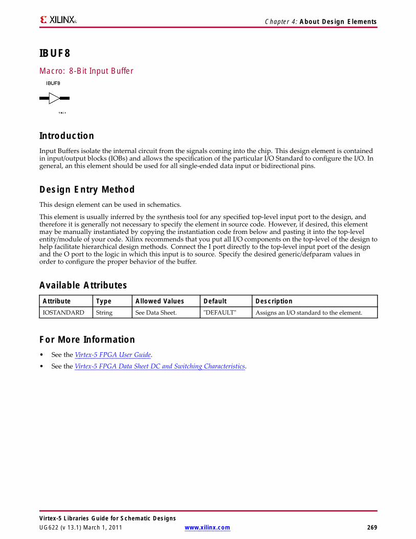
Chapter 4: About Design Elements
IBUF8Macro: 8-Bit Input Buffer
IntroductionInput Buffers isolate the internal circuit from the signals coming into the chip. This design element is containedin input/output blocks (IOBs) and allows the specification of the particular I/O Standard to configure the I/O. Ingeneral, an this element should be used for all single-ended data input or bidirectional pins.
Design Entry MethodThis design element can be used in schematics.
This element is usually inferred by the synthesis tool for any specified top-level input port to the design, andtherefore it is generally not necessary to specify the element in source code. However, if desired, this elementmay be manually instantiated by copying the instantiation code from below and pasting it into the top-levelentity/module of your code. Xilinx recommends that you put all I/O components on the top-level of the design tohelp facilitate hierarchical design methods. Connect the I port directly to the top-level input port of the designand the O port to the logic in which this input is to source. Specify the desired generic/defparam values inorder to configure the proper behavior of the buffer.
Available AttributesAttribute Type Allowed Values Default DescriptionIOSTANDARD String See Data Sheet. "DEFAULT" Assigns an I/O standard to the element.
For More Information• See the Virtex-5 FPGA User Guide.
• See the Virtex-5 FPGA Data Sheet DC and Switching Characteristics.
Virtex-5 Libraries Guide for Schematic DesignsUG622 (v 13.1) March 1, 2011 www.xilinx.com 269

Chapter 4: About Design Elements
IBUFDSPrimitive: Differential Signaling Input Buffer
IntroductionThis design element is an input buffer that supports low-voltage, differential signaling. In IBUFDS, a designlevel interface signal is represented as two distinct ports (I and IB), one deemed the "master" and the other the"slave." The master and the slave are opposite phases of the same logical signal (for example, MYNET_P andMYNET_N). Optionally, a programmable differential termination feature is available to help improve signalintegrity and reduce external components.
Logic TableInputs Outputs
I IB O0 0 No Change
0 1 0
1 0 1
1 1 No Change
Port DescriptionsPort Type Width FunctionI Input 1 Diff_p Buffer Input
IB Input 1 Diff_n Buffer Input
O Output 1 Buffer Output
Design Entry MethodThis design element can be used in schematics.
Put all I/O components on the top-level of the design to help facilitate hierarchical design methods. Connectthe I port directly to the top-level "master" input port of the design, the IB port to the top-level "slave" inputport, and the O port to the logic in which this input is to source. Specify the desired generic/defparam values inorder to configure the proper behavior of the buffer.
Available Attributes
Attribute TypeAllowedValues Default Description
DIFF_TERM Boolean TRUE or FALSE FALSE Enables the built-in differential terminationresistor.
IOSTANDARD String See Data Sheet. "DEFAULT" Assigns an I/O standard to the element.
Virtex-5 Libraries Guide for Schematic Designs270 www.xilinx.com UG622 (v 13.1) March 1, 2011

Chapter 4: About Design Elements
For More Information• See the Virtex-5 FPGA User Guide.
• See the Virtex-5 FPGA Data Sheet DC and Switching Characteristics.
Virtex-5 Libraries Guide for Schematic DesignsUG622 (v 13.1) March 1, 2011 www.xilinx.com 271
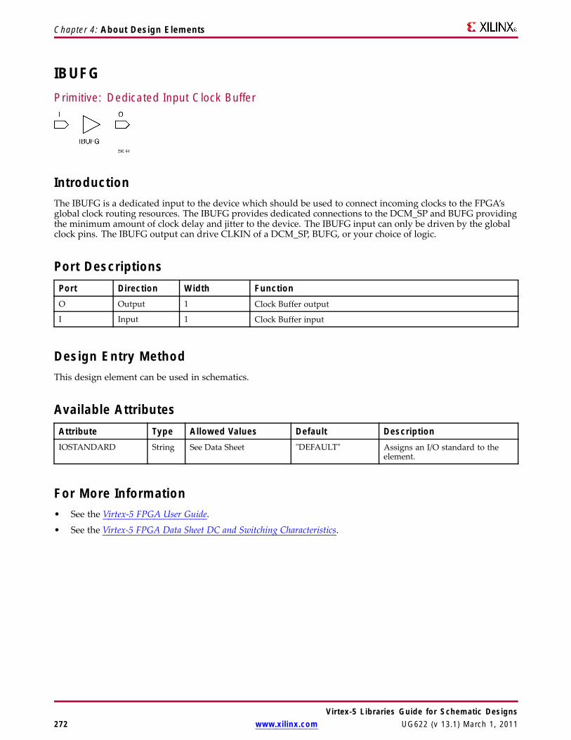
Chapter 4: About Design Elements
IBUFGPrimitive: Dedicated Input Clock Buffer
IntroductionThe IBUFG is a dedicated input to the device which should be used to connect incoming clocks to the FPGA’sglobal clock routing resources. The IBUFG provides dedicated connections to the DCM_SP and BUFG providingthe minimum amount of clock delay and jitter to the device. The IBUFG input can only be driven by the globalclock pins. The IBUFG output can drive CLKIN of a DCM_SP, BUFG, or your choice of logic.
Port DescriptionsPort Direction Width FunctionO Output 1 Clock Buffer output
I Input 1 Clock Buffer input
Design Entry MethodThis design element can be used in schematics.
Available AttributesAttribute Type Allowed Values Default DescriptionIOSTANDARD String See Data Sheet "DEFAULT" Assigns an I/O standard to the
element.
For More Information• See the Virtex-5 FPGA User Guide.
• See the Virtex-5 FPGA Data Sheet DC and Switching Characteristics.
Virtex-5 Libraries Guide for Schematic Designs272 www.xilinx.com UG622 (v 13.1) March 1, 2011
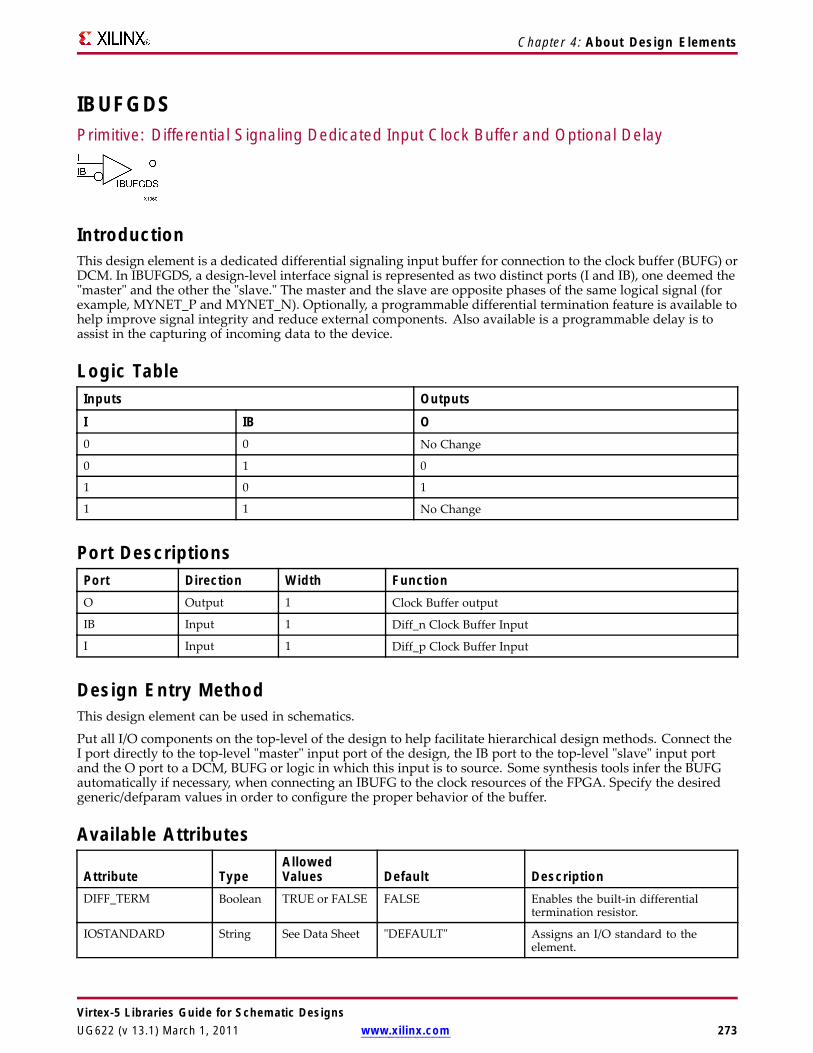
Chapter 4: About Design Elements
IBUFGDSPrimitive: Differential Signaling Dedicated Input Clock Buffer and Optional Delay
IntroductionThis design element is a dedicated differential signaling input buffer for connection to the clock buffer (BUFG) orDCM. In IBUFGDS, a design-level interface signal is represented as two distinct ports (I and IB), one deemed the"master" and the other the "slave." The master and the slave are opposite phases of the same logical signal (forexample, MYNET_P and MYNET_N). Optionally, a programmable differential termination feature is available tohelp improve signal integrity and reduce external components. Also available is a programmable delay is toassist in the capturing of incoming data to the device.
Logic TableInputs Outputs
I IB O0 0 No Change
0 1 0
1 0 1
1 1 No Change
Port DescriptionsPort Direction Width FunctionO Output 1 Clock Buffer output
IB Input 1 Diff_n Clock Buffer Input
I Input 1 Diff_p Clock Buffer Input
Design Entry MethodThis design element can be used in schematics.
Put all I/O components on the top-level of the design to help facilitate hierarchical design methods. Connect theI port directly to the top-level "master" input port of the design, the IB port to the top-level "slave" input portand the O port to a DCM, BUFG or logic in which this input is to source. Some synthesis tools infer the BUFGautomatically if necessary, when connecting an IBUFG to the clock resources of the FPGA. Specify the desiredgeneric/defparam values in order to configure the proper behavior of the buffer.
Available Attributes
Attribute TypeAllowedValues Default Description
DIFF_TERM Boolean TRUE or FALSE FALSE Enables the built-in differentialtermination resistor.
IOSTANDARD String See Data Sheet "DEFAULT" Assigns an I/O standard to theelement.
Virtex-5 Libraries Guide for Schematic DesignsUG622 (v 13.1) March 1, 2011 www.xilinx.com 273

Chapter 4: About Design Elements
For More Information• See the Virtex-5 FPGA User Guide.
• See the Virtex-5 FPGA Data Sheet DC and Switching Characteristics.
Virtex-5 Libraries Guide for Schematic Designs274 www.xilinx.com UG622 (v 13.1) March 1, 2011
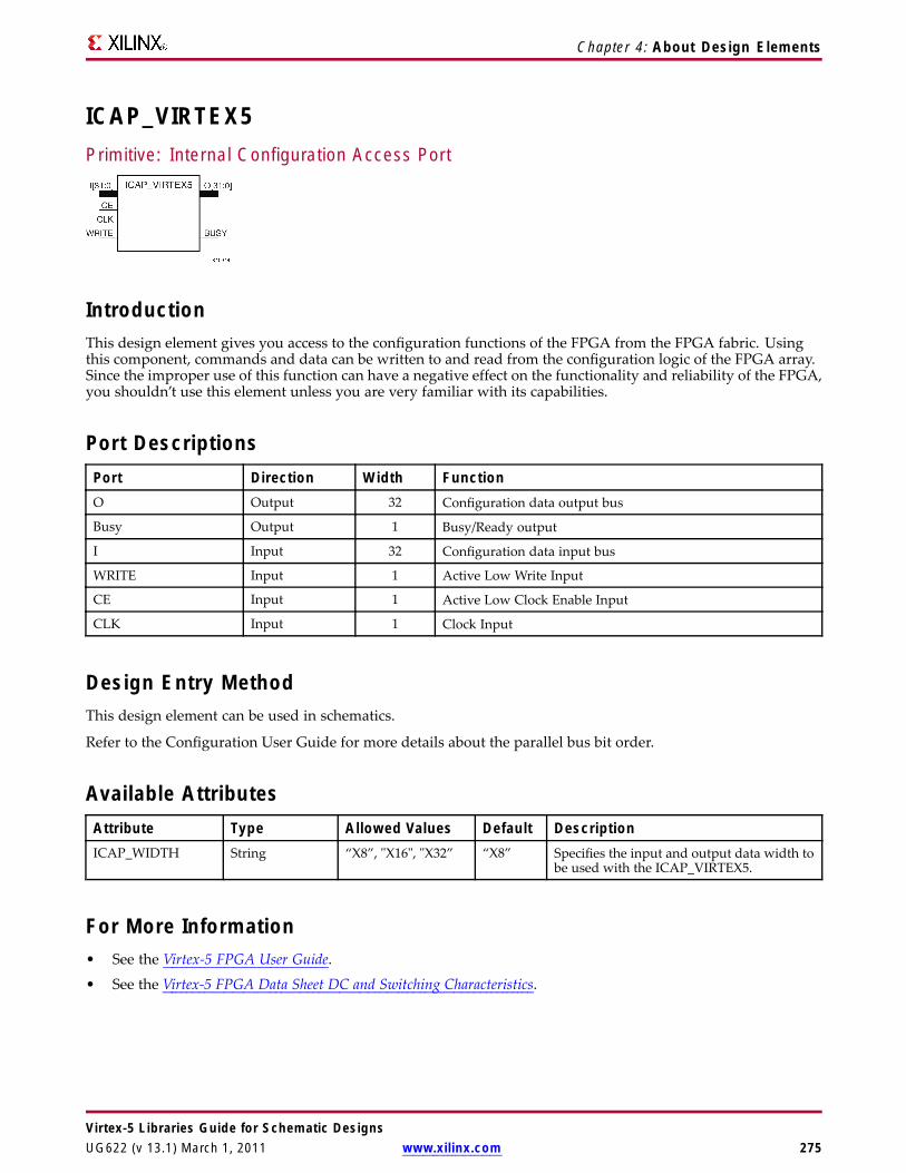
Chapter 4: About Design Elements
ICAP_VIRTEX5Primitive: Internal Configuration Access Port
IntroductionThis design element gives you access to the configuration functions of the FPGA from the FPGA fabric. Usingthis component, commands and data can be written to and read from the configuration logic of the FPGA array.Since the improper use of this function can have a negative effect on the functionality and reliability of the FPGA,you shouldn’t use this element unless you are very familiar with its capabilities.
Port DescriptionsPort Direction Width FunctionO Output 32 Configuration data output bus
Busy Output 1 Busy/Ready output
I Input 32 Configuration data input bus
WRITE Input 1 Active Low Write Input
CE Input 1 Active Low Clock Enable Input
CLK Input 1 Clock Input
Design Entry MethodThis design element can be used in schematics.
Refer to the Configuration User Guide for more details about the parallel bus bit order.
Available AttributesAttribute Type Allowed Values Default DescriptionICAP_WIDTH String “X8”, "X16", "X32” “X8” Specifies the input and output data width to
be used with the ICAP_VIRTEX5.
For More Information• See the Virtex-5 FPGA User Guide.
• See the Virtex-5 FPGA Data Sheet DC and Switching Characteristics.
Virtex-5 Libraries Guide for Schematic DesignsUG622 (v 13.1) March 1, 2011 www.xilinx.com 275
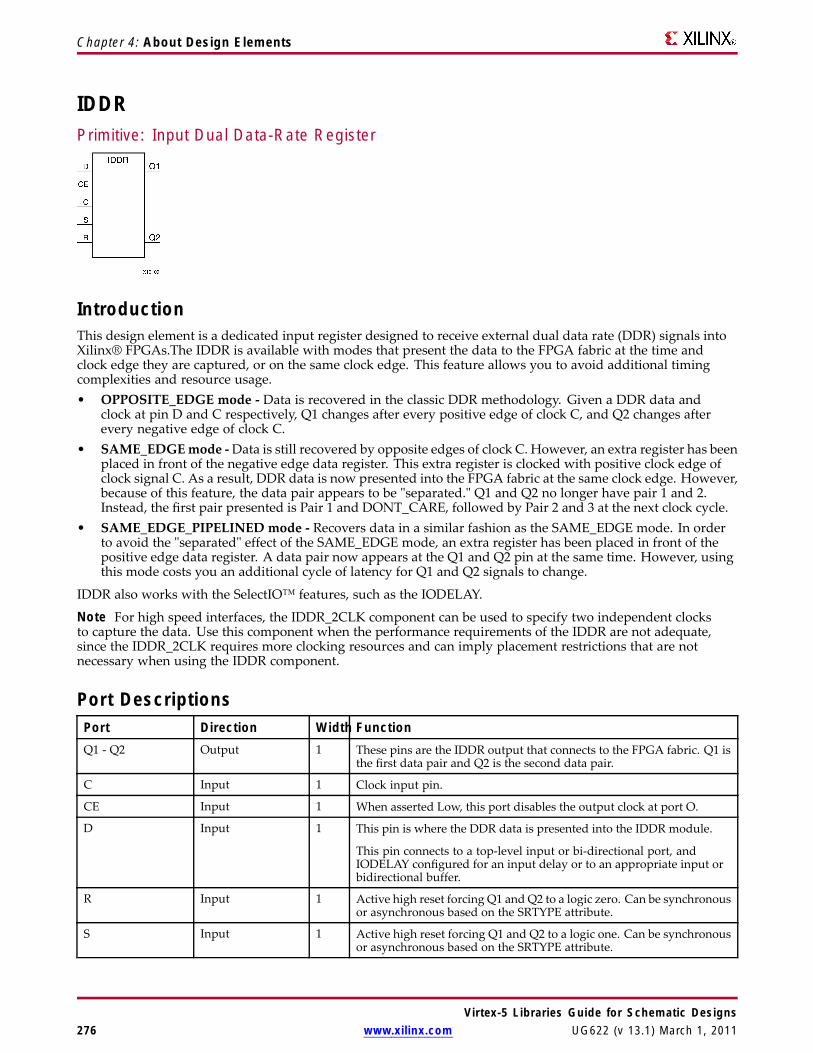
Chapter 4: About Design Elements
IDDRPrimitive: Input Dual Data-Rate Register
IntroductionThis design element is a dedicated input register designed to receive external dual data rate (DDR) signals intoXilinx® FPGAs.The IDDR is available with modes that present the data to the FPGA fabric at the time andclock edge they are captured, or on the same clock edge. This feature allows you to avoid additional timingcomplexities and resource usage.• OPPOSITE_EDGE mode - Data is recovered in the classic DDR methodology. Given a DDR data and
clock at pin D and C respectively, Q1 changes after every positive edge of clock C, and Q2 changes afterevery negative edge of clock C.
• SAME_EDGEmode -Data is still recovered by opposite edges of clock C. However, an extra register has beenplaced in front of the negative edge data register. This extra register is clocked with positive clock edge ofclock signal C. As a result, DDR data is now presented into the FPGA fabric at the same clock edge. However,because of this feature, the data pair appears to be "separated." Q1 and Q2 no longer have pair 1 and 2.Instead, the first pair presented is Pair 1 and DONT_CARE, followed by Pair 2 and 3 at the next clock cycle.
• SAME_EDGE_PIPELINED mode - Recovers data in a similar fashion as the SAME_EDGE mode. In orderto avoid the "separated" effect of the SAME_EDGE mode, an extra register has been placed in front of thepositive edge data register. A data pair now appears at the Q1 and Q2 pin at the same time. However, usingthis mode costs you an additional cycle of latency for Q1 and Q2 signals to change.
IDDR also works with the SelectIO™ features, such as the IODELAY.
Note For high speed interfaces, the IDDR_2CLK component can be used to specify two independent clocksto capture the data. Use this component when the performance requirements of the IDDR are not adequate,since the IDDR_2CLK requires more clocking resources and can imply placement restrictions that are notnecessary when using the IDDR component.
Port DescriptionsPort Direction Width FunctionQ1 - Q2 Output 1 These pins are the IDDR output that connects to the FPGA fabric. Q1 is
the first data pair and Q2 is the second data pair.
C Input 1 Clock input pin.
CE Input 1 When asserted Low, this port disables the output clock at port O.
D Input 1 This pin is where the DDR data is presented into the IDDR module.
This pin connects to a top-level input or bi-directional port, andIODELAY configured for an input delay or to an appropriate input orbidirectional buffer.
R Input 1 Active high reset forcing Q1 and Q2 to a logic zero. Can be synchronousor asynchronous based on the SRTYPE attribute.
S Input 1 Active high reset forcing Q1 and Q2 to a logic one. Can be synchronousor asynchronous based on the SRTYPE attribute.
Virtex-5 Libraries Guide for Schematic Designs276 www.xilinx.com UG622 (v 13.1) March 1, 2011
Chapter 4: About Design Elements
Design Entry MethodThis design element can be used in schematics.
Available AttributesAttribute Type Allowed Values Default DescriptionDDR_CLK_EDGE String "OPPOSITE_EDGE",
"SAME_EDGE","SAME_EDGE_PIPELINED"
"OPPOSITE_EDGE”
Sets the IDDR mode of operation withrespect to clock edge.
INIT_Q1 Binary 0, 1 0 Initial value on the Q1 pin afterconfiguration startup or when GSR isasserted.
INIT_Q2 Binary 0, 1 0 Initial value on the Q2 pin afterconfiguration startup or when GSR isasserted.
SRTYPE String "SYNC" or "ASYNC” "SYNC” Set/reset type selection. "SYNC" specifiesthe behavior of the reset (R) and set (S)pins to be synchronous to the positive edgeof the C clock pin. "ASYNC" specifies anasynchronous set/reset function.
For More Information• See the Virtex-5 FPGA User Guide.
• See the Virtex-5 FPGA Data Sheet DC and Switching Characteristics.
Virtex-5 Libraries Guide for Schematic DesignsUG622 (v 13.1) March 1, 2011 www.xilinx.com 277

Chapter 4: About Design Elements
IDDR_2CLKPrimitive: Input Dual Data-Rate Register with Dual Clock Inputs
IntroductionThis design element is a dedicated input register designed to receive external dual data rate (DDR) signals intoXilinx® FPGAs. In general, you should only use the IDDR_2CLK for applications in which two clocks arerequired to capture the rising and falling data for DDR applications.
• OPPOSITE_EDGE mode - Data is presented in the classic DDR methodology. Given a DDR data andclock at pin D and C respectively, Q1 changes after every positive edge of clock C, and Q2 changes afterevery positive edge of clock CB.
• SAME_EDGE mode - Data is still presented by positive edges of each clock. However, an extra register hasbeen placed in front of the CB clocked data register. This extra register is clocked with positive clock edge ofclock signal C. As a result, DDR data is now presented into the FPGA fabric at the positive edge of clock C.However, because of this feature, the data pair appears to be "separated." Q1 and Q2 no longer have pair 1 and2. Instead, the first pair presented is Pair 1 and DON’T CARE, followed by Pair 2 and 3 at the next clock cycle.
• SAME_EDGE_PIPELINED mode - Presents data in a similar fashion as the SAME_EDGE mode. In order toavoid the "separated" effect of the SAME_EDGE mode, an extra register has been placed in front of the Cclocked data register. A data pair now appears at the Q1 and Q2 pin at the same time during the positive edgeof C. However, using this mode, costs you an additional cycle of latency for Q1 and Q2 signals to change.
IDDR also works with SelectIO™ features, such as the IODELAY.
Port DescriptionsPort Direction Width FunctionQ1 : Q2 Output 1 These pins are the IDDR output that connects to the FPGA
fabric. Q1 is the first data pair and Q2 is the second data pair.
C Input 1 Primary clock input pin used to capture the positive edgedata.
CB Input 1 Secondary clock input pin (typically 180 degrees out ofphase with the primary clock) used to capture the negativeedge data.
CE Input 1 When asserted Low, this port disables the output clock atport O.
D Input 1 This pin is where the DDR data is presented into the IDDRmodule.
This pin connects to a top-level input or bi-directionalport, and IODELAY configured for an input delay or to anappropriate input or bidirectional buffer.
R Input 1 Active high reset forcing Q1 and Q2 to a logic zero. Canbe synchronous or asynchronous based on the SRTYPEattribute.
Virtex-5 Libraries Guide for Schematic Designs278 www.xilinx.com UG622 (v 13.1) March 1, 2011

Chapter 4: About Design Elements
Port Direction Width FunctionS Input 1 Active high reset forcing Q1 and Q2 to a logic one. Can
be synchronous or asynchronous based on the SRTYPEattribute.
Design Entry MethodThis design element can be used in schematics.
• Connect the C pin to the appropriate clock source, representing the positive clock edge and CB to theclock source representing the negative clock edge.
• Connect the D pin to the top-level input, or bidirectional port, an IODELAY, or an instantiated inputor bidirectional buffer.
• The Q1 and Q2 pins should be connected to the appropriate data sources.
• CE should be tied high when not used, or connected to the appropriate clock enable logic.
• R and S pins should be tied low, if not used, or to the appropriate set or reset generation logic.
• Set all attributes to the component to represent the desired behavior.
• Always instantiate this component in pairs with the same clocking, and to LOC those to the appropriate Pand N I/O pair in order not to sacrifice possible I/O resources.
• Always instantiate this component in the top-level hierarchy of your design, along with any otherinstantiated I/O components for the design. This helps facilitate hierarchical design flows/practices.
• To minimize CLK skew, both CLK and CLKB should come from global routing (DCM / MMCM) and notfrom the local inversion. DCM / MMCM de-skews these clocks whereas the local inversion adds skew.
Available AttributesAttribute Type Allowed Values Default DescriptionDDR_CLK_EDGE String "OPPOSITE_EDGE",
"SAME_EDGE""SAME_EDGE_PIPELINED"
"OPPOSITE_EDGE”
DDR clock mode recovery modeselection. See Introduction for moreexplanation.
INIT_Q1 Binary 0, 1 0 Initial value on the Q1 pin afterconfiguration startup or when GSR isasserted.
INIT_Q2 Binary 0, 1 0 Initial value on the Q2 pin afterconfiguration startup or when GSR isasserted.
SRTYPE String "SYNC" or "ASYNC” "SYNC” Set/reset type selection. SYNC"specifies the behavior of the reset (R)and set (S) pins to be synchronous tothe positive edge of the C clock pin."ASYNC" specifies an asynchronousset/reset function.
Virtex-5 Libraries Guide for Schematic DesignsUG622 (v 13.1) March 1, 2011 www.xilinx.com 279

Chapter 4: About Design Elements
IDELAYCTRLPrimitive: IDELAY Tap Delay Value Control
IntroductionThis design element must be instantiated when using the IODELAYE1. This occurs when the IDELAY or ISERDESprimitive is instantiated with the IOBDELAY_TYPE attribute set to Fixed or Variable. The IDELAYCTRL moduleprovides a voltage bias, independent of process, voltage, and temperature variations to the tap-delay line using afixed-frequency reference clock, REFCLK. This enables very accurate delay tuning.
Port DescriptionsPort Type Width FunctionRDY Output 1 Indicates the validity of the reference clock input, REFCLK. When
REFCLK disappears (i.e., REFCLK is held High or Low for one clockperiod or more), the RDY signal is deasserted.
REFCLK Input 1 Provides a voltage bias, independent of process, voltage, andtemperature variations, to the tap-delay lines in the IOBs. Thefrequency of REFCLK must be 200 MHz to guarantee the tap-delayvalue specified in the applicable data sheet.
RST Input 1 Resets the IDELAYCTRL circuitry. The RST signal is an active-highasynchronous reset. To reset the IDELAYCTRL, assert it High for atleast 50 ns.
RST (Module reset) - Resets the IDELAYCTRL circuitry. The RST signal is an active-high asynchronous reset. Toreset the IDELAYCTRL, assert it High for at least 50 ns.
REFCLK (Reference Clock) - Provides a voltage bias, independent of process, voltage, and temperaturevariations, to the tap-delay lines in the IOBs. The frequency of REFCLK must be 200 MHz to guarantee thetap-delay value specified in the applicable data sheet.
RDY (Ready Output) - Indicates the validity of the reference clock input, REFCLK. When REFCLK disappears(i.e., REFCLK is held High or Low for one clock period or more), the RDY signal is deasserted.
Design Entry MethodThis design element can be used in schematics.
For More Information• See the Virtex-5 FPGA User Guide.
• See the Virtex-5 FPGA Data Sheet DC and Switching Characteristics.
Virtex-5 Libraries Guide for Schematic Designs280 www.xilinx.com UG622 (v 13.1) March 1, 2011
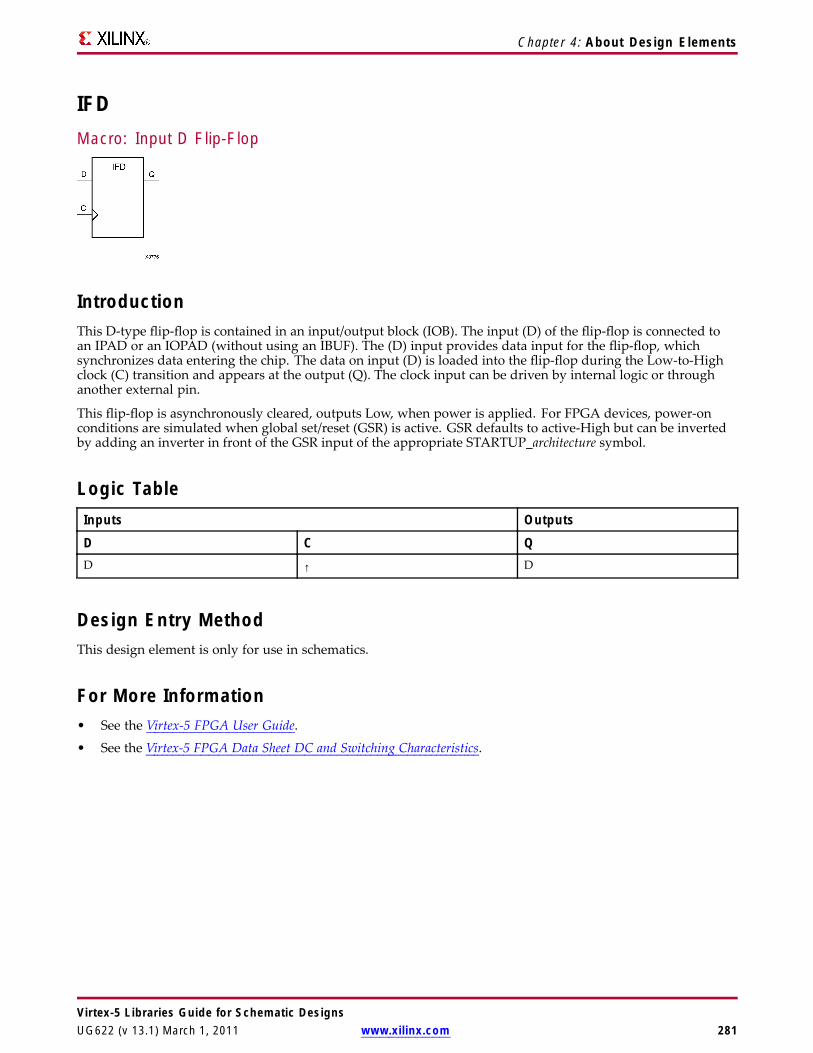
Chapter 4: About Design Elements
IFDMacro: Input D Flip-Flop
IntroductionThis D-type flip-flop is contained in an input/output block (IOB). The input (D) of the flip-flop is connected toan IPAD or an IOPAD (without using an IBUF). The (D) input provides data input for the flip-flop, whichsynchronizes data entering the chip. The data on input (D) is loaded into the flip-flop during the Low-to-Highclock (C) transition and appears at the output (Q). The clock input can be driven by internal logic or throughanother external pin.
This flip-flop is asynchronously cleared, outputs Low, when power is applied. For FPGA devices, power-onconditions are simulated when global set/reset (GSR) is active. GSR defaults to active-High but can be invertedby adding an inverter in front of the GSR input of the appropriate STARTUP_architecture symbol.
Logic TableInputs Outputs
D C QD ↑ D
Design Entry MethodThis design element is only for use in schematics.
For More Information• See the Virtex-5 FPGA User Guide.
• See the Virtex-5 FPGA Data Sheet DC and Switching Characteristics.
Virtex-5 Libraries Guide for Schematic DesignsUG622 (v 13.1) March 1, 2011 www.xilinx.com 281

Chapter 4: About Design Elements
IFD_1Macro: Input D Flip-Flop with Inverted Clock (Asynchronous Preset)
IntroductionThis design element is a D-type flip flop which is contained in an input/output block (IOB). The input (D) of theflip-flop is connected to an IPAD or an IOPAD. The D input also provides data input for the flip-flop, whichsynchronizes data entering the chip. The D input data is loaded into the flip-flop during the High-to-Lowclock (C) transition and appears at the output (Q). The clock input can be driven by internal logic or throughanother external pin.
This flip-flop is asynchronously cleared, outputs Low, when power is applied. For FPGA devices, power-onconditions are simulated when global set/reset (GSR) is active. GSR defaults to active-High but can be invertedby adding an inverter in front of the GSR input of the appropriate STARTUP_architecture symbol.
Logic TableInputs Outputs
D C Q0 ↓ 0
1 ↓ 1
Design Entry MethodThis design element is only for use in schematics.
For More Information• See the Virtex-5 FPGA User Guide.
• See the Virtex-5 FPGA Data Sheet DC and Switching Characteristics.
Virtex-5 Libraries Guide for Schematic Designs282 www.xilinx.com UG622 (v 13.1) March 1, 2011

Chapter 4: About Design Elements
IFD16Macro: 16-Bit Input D Flip-Flop
IntroductionThis D-type flip-flop is contained in an input/output block (IOB). The input (D) of the flip-flop is connected toan IPAD or an IOPAD (without using an IBUF). The (D) input provides data input for the flip-flop, whichsynchronizes data entering the chip. The data on input (D) is loaded into the flip-flop during the Low-to-Highclock (C) transition and appears at the output (Q). The clock input can be driven by internal logic or throughanother external pin.
This flip-flop is asynchronously cleared, outputs Low, when power is applied. For FPGA devices, power-onconditions are simulated when global set/reset (GSR) is active. GSR defaults to active-High but can be invertedby adding an inverter in front of the GSR input of the appropriate STARTUP_architecture symbol.
Logic TableInputs Outputs
D C QD ↑ D
Design Entry MethodThis design element is only for use in schematics.
For More Information• See the Virtex-5 FPGA User Guide.
• See the Virtex-5 FPGA Data Sheet DC and Switching Characteristics.
Virtex-5 Libraries Guide for Schematic DesignsUG622 (v 13.1) March 1, 2011 www.xilinx.com 283

Chapter 4: About Design Elements
IFD4Macro: 4-Bit Input D Flip-Flop
IntroductionThis D-type flip-flop is contained in an input/output block (IOB). The input (D) of the flip-flop is connected toan IPAD or an IOPAD (without using an IBUF). The (D) input provides data input for the flip-flop, whichsynchronizes data entering the chip. The data on input (D) is loaded into the flip-flop during the Low-to-Highclock (C) transition and appears at the output (Q). The clock input can be driven by internal logic or throughanother external pin.
This flip-flop is asynchronously cleared, outputs Low, when power is applied. For FPGA devices, power-onconditions are simulated when global set/reset (GSR) is active. GSR defaults to active-High but can be invertedby adding an inverter in front of the GSR input of the appropriate STARTUP_architecture symbol.
Logic TableInputs Outputs
D C QD ↑ D
Design Entry MethodThis design element is only for use in schematics.
For More Information• See the Virtex-5 FPGA User Guide.
• See the Virtex-5 FPGA Data Sheet DC and Switching Characteristics.
Virtex-5 Libraries Guide for Schematic Designs284 www.xilinx.com UG622 (v 13.1) March 1, 2011

Chapter 4: About Design Elements
IFD8Macro: 8-Bit Input D Flip-Flop
IntroductionThis D-type flip-flop is contained in an input/output block (IOB). The input (D) of the flip-flop is connected toan IPAD or an IOPAD (without using an IBUF). The (D) input provides data input for the flip-flop, whichsynchronizes data entering the chip. The data on input (D) is loaded into the flip-flop during the Low-to-Highclock (C) transition and appears at the output (Q). The clock input can be driven by internal logic or throughanother external pin.
This flip-flop is asynchronously cleared, outputs Low, when power is applied. For FPGA devices, power-onconditions are simulated when global set/reset (GSR) is active. GSR defaults to active-High but can be invertedby adding an inverter in front of the GSR input of the appropriate STARTUP_architecture symbol.
Logic TableInputs Outputs
D C QD ↑ D
Design Entry MethodThis design element is only for use in schematics.
For More Information• See the Virtex-5 FPGA User Guide.
• See the Virtex-5 FPGA Data Sheet DC and Switching Characteristics.
Virtex-5 Libraries Guide for Schematic DesignsUG622 (v 13.1) March 1, 2011 www.xilinx.com 285

Chapter 4: About Design Elements
IFDIMacro: Input D Flip-Flop (Asynchronous Preset)
IntroductionThis design element is a D-type flip-flop which is contained in an input/output block (IOB). The input (D) ofthe flip-flop is connected to an IPAD or an IOPAD. The D input provides data input for the flip-flop, whichsynchronizes data entering the chip. The D input data is loaded into the flip-flop during the Low-to-Highclock (C) transition and appears at the output (Q). The clock input can be driven by internal logic or throughanother external pin.
This flip-flop is asynchronously cleared, outputs Low, when power is applied. For FPGA devices, power-onconditions are simulated when global set/reset (GSR) is active. GSR defaults to active-High but can be invertedby adding an inverter in front of the GSR input of the appropriate STARTUP_architecture symbol.
Logic TableInputs Outputs
D C QD ↑ D
Design Entry MethodThis design element is only for use in schematics.
For More Information• See the Virtex-5 FPGA User Guide.
• See the Virtex-5 FPGA Data Sheet DC and Switching Characteristics.
Virtex-5 Libraries Guide for Schematic Designs286 www.xilinx.com UG622 (v 13.1) March 1, 2011

Chapter 4: About Design Elements
IFDI_1Macro: Input D Flip-Flop with Inverted Clock (Asynchronous Preset)
IntroductionThe design element is a D-type flip-flop is contained in an input/output block (IOB). The input (D) of the flip-flopis connected to an IPAD or an IOPAD. The (D) input provides data input for the flip-flop, which synchronizes dataentering the chip. The data on input (D) is loaded into the flip-flop during the High-to-Low clock (C) transitionand appears at the output (Q). The clock input can be driven by internal logic or through another external pin.
This flip-flop is asynchronously cleared, outputs Low, when power is applied. For FPGA devices, power-onconditions are simulated when global set/reset (GSR) is active. GSR defaults to active-High but can be invertedby adding an inverter in front of the GSR input of the appropriate STARTUP_architecture symbol.
Logic TableInputs Outputs
D C Q0 ↓ 0
1 ↓ 1
Design Entry MethodThis design element is only for use in schematics.
For More Information• See the Virtex-5 FPGA User Guide.
• See the Virtex-5 FPGA Data Sheet DC and Switching Characteristics.
Virtex-5 Libraries Guide for Schematic DesignsUG622 (v 13.1) March 1, 2011 www.xilinx.com 287

Chapter 4: About Design Elements
IFDXMacro: Input D Flip-Flop with Clock Enable
IntroductionThis D-type flip-flop is contained in an input/output block (IOB). The input (D) of the flip-flop is connectedto an IPAD or an IOPAD (without using an IBUF). The D input provides data input for the flip-flop, whichsynchronizes data entering the chip. When CE is High, the data on input D is loaded into the flip-flop during theLow-to-High clock (C) transition and appears at the output (Q). The clock input can be driven by internal logic orthrough another external pin. When CE is Low, flip-flop outputs do not change.
This flip-flop is asynchronously cleared, outputs Low, when power is applied. For FPGA devices, power-onconditions are simulated when global set/reset (GSR) is active. GSR defaults to active-High but can be invertedby adding an inverter in front of the GSR input of the appropriate STARTUP_architecture symbol.
Logic TableInputs Outputs
CE D C Q1 D ↑ D
0 X X No Change
Design Entry MethodThis design element is only for use in schematics.
For More Information• See the Virtex-5 FPGA User Guide.
• See the Virtex-5 FPGA Data Sheet DC and Switching Characteristics.
Virtex-5 Libraries Guide for Schematic Designs288 www.xilinx.com UG622 (v 13.1) March 1, 2011
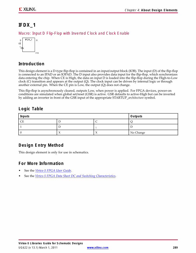
Chapter 4: About Design Elements
IFDX_1Macro: Input D Flip-Flop with Inverted Clock and Clock Enable
IntroductionThis design element is a D-type flip-flop is contained in an input/output block (IOB). The input (D) of the flip-flopis connected to an IPAD or an IOPAD. The D input also provides data input for the flip-flop, which synchronizesdata entering the chip. When CE is High, the data on input D is loaded into the flip-flop during the High-to-Lowclock (C) transition and appears at the output (Q). The clock input can be driven by internal logic or throughanother external pin. When the CE pin is Low, the output (Q) does not change.
This flip-flop is asynchronously cleared, outputs Low, when power is applied. For FPGA devices, power-onconditions are simulated when global set/reset (GSR) is active. GSR defaults to active-High but can be invertedby adding an inverter in front of the GSR input of the appropriate STARTUP_architecture symbol.
Logic TableInputs OutputsCE D C Q
1 D ↓ D
0 X X No Change
Design Entry MethodThis design element is only for use in schematics.
For More Information• See the Virtex-5 FPGA User Guide.
• See the Virtex-5 FPGA Data Sheet DC and Switching Characteristics.
Virtex-5 Libraries Guide for Schematic DesignsUG622 (v 13.1) March 1, 2011 www.xilinx.com 289
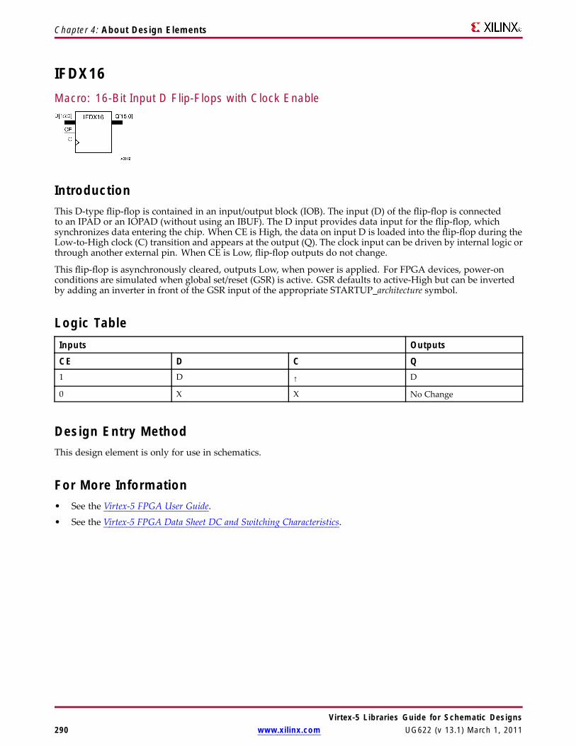
Chapter 4: About Design Elements
IFDX16Macro: 16-Bit Input D Flip-Flops with Clock Enable
IntroductionThis D-type flip-flop is contained in an input/output block (IOB). The input (D) of the flip-flop is connectedto an IPAD or an IOPAD (without using an IBUF). The D input provides data input for the flip-flop, whichsynchronizes data entering the chip. When CE is High, the data on input D is loaded into the flip-flop during theLow-to-High clock (C) transition and appears at the output (Q). The clock input can be driven by internal logic orthrough another external pin. When CE is Low, flip-flop outputs do not change.
This flip-flop is asynchronously cleared, outputs Low, when power is applied. For FPGA devices, power-onconditions are simulated when global set/reset (GSR) is active. GSR defaults to active-High but can be invertedby adding an inverter in front of the GSR input of the appropriate STARTUP_architecture symbol.
Logic TableInputs Outputs
CE D C Q1 D ↑ D
0 X X No Change
Design Entry MethodThis design element is only for use in schematics.
For More Information• See the Virtex-5 FPGA User Guide.
• See the Virtex-5 FPGA Data Sheet DC and Switching Characteristics.
Virtex-5 Libraries Guide for Schematic Designs290 www.xilinx.com UG622 (v 13.1) March 1, 2011

Chapter 4: About Design Elements
IFDX4Macro: 4-Bit Input D Flip-Flop with Clock Enable
IntroductionThis D-type flip-flop is contained in an input/output block (IOB). The input (D) of the flip-flop is connectedto an IPAD or an IOPAD (without using an IBUF). The D input provides data input for the flip-flop, whichsynchronizes data entering the chip. When CE is High, the data on input D is loaded into the flip-flop during theLow-to-High clock (C) transition and appears at the output (Q). The clock input can be driven by internal logic orthrough another external pin. When CE is Low, flip-flop outputs do not change.
This flip-flop is asynchronously cleared, outputs Low, when power is applied. For FPGA devices, power-onconditions are simulated when global set/reset (GSR) is active. GSR defaults to active-High but can be invertedby adding an inverter in front of the GSR input of the appropriate STARTUP_architecture symbol.
Logic TableInputs Outputs
CE D C Q1 D ↑ D
0 X X No Change
Design Entry MethodThis design element is only for use in schematics.
For More Information• See the Virtex-5 FPGA User Guide.
• See the Virtex-5 FPGA Data Sheet DC and Switching Characteristics.
Virtex-5 Libraries Guide for Schematic DesignsUG622 (v 13.1) March 1, 2011 www.xilinx.com 291
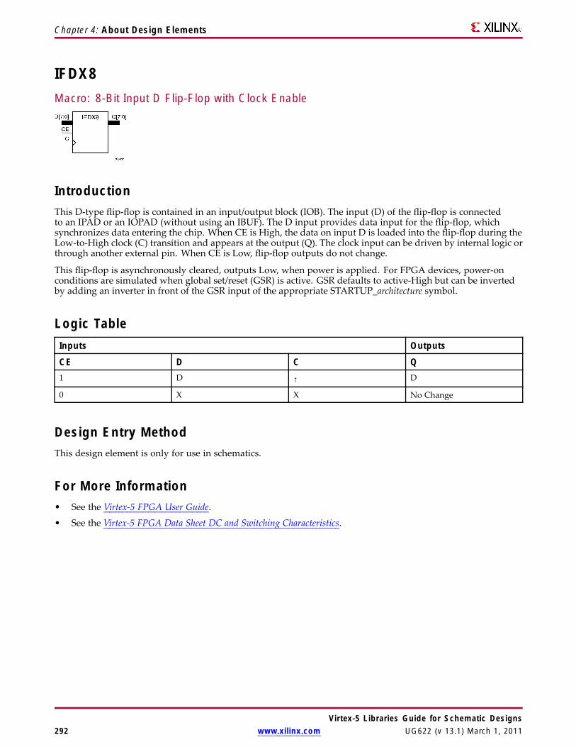
Chapter 4: About Design Elements
IFDX8Macro: 8-Bit Input D Flip-Flop with Clock Enable
IntroductionThis D-type flip-flop is contained in an input/output block (IOB). The input (D) of the flip-flop is connectedto an IPAD or an IOPAD (without using an IBUF). The D input provides data input for the flip-flop, whichsynchronizes data entering the chip. When CE is High, the data on input D is loaded into the flip-flop during theLow-to-High clock (C) transition and appears at the output (Q). The clock input can be driven by internal logic orthrough another external pin. When CE is Low, flip-flop outputs do not change.
This flip-flop is asynchronously cleared, outputs Low, when power is applied. For FPGA devices, power-onconditions are simulated when global set/reset (GSR) is active. GSR defaults to active-High but can be invertedby adding an inverter in front of the GSR input of the appropriate STARTUP_architecture symbol.
Logic TableInputs Outputs
CE D C Q1 D ↑ D
0 X X No Change
Design Entry MethodThis design element is only for use in schematics.
For More Information• See the Virtex-5 FPGA User Guide.
• See the Virtex-5 FPGA Data Sheet DC and Switching Characteristics.
Virtex-5 Libraries Guide for Schematic Designs292 www.xilinx.com UG622 (v 13.1) March 1, 2011

Chapter 4: About Design Elements
ILDMacro: Transparent Input Data Latch
IntroductionThis design element is a single, transparent data latch that holds transient data entering a chip. This latch iscontained in an input/output block (IOB). The latch input (D) is connected to an IPAD or an IOPAD (withoutusing an IBUF). When the gate input (G) is High, data on the input (D) appears on the output (Q). Data on the Dinput during the High-to-Low G transition is stored in the latch.
This latch is asynchronously cleared, outputs Low, when power is applied. For FPGA devices, power-onconditions are simulated when global set/reset (GSR) is active. GSR defaults to active-High but can be invertedby adding an inverter in front of the GSR input of the appropriate STARTUP_architecture symbol.
Logic TableInputs Output
G D Q1 D D
0 X No Change
↓ D D
Design Entry MethodThis design element is only for use in schematics.
For More Information• See the Virtex-5 FPGA User Guide.
• See the Virtex-5 FPGA Data Sheet DC and Switching Characteristics.
Virtex-5 Libraries Guide for Schematic DesignsUG622 (v 13.1) March 1, 2011 www.xilinx.com 293
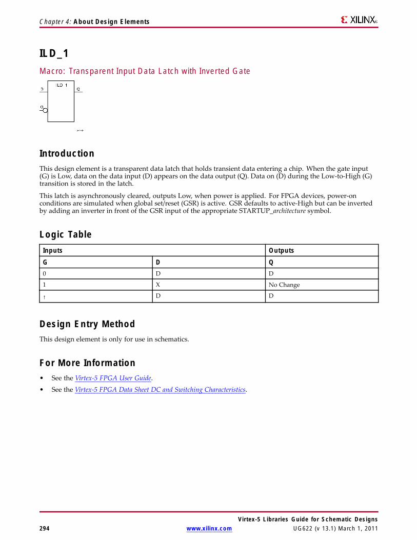
Chapter 4: About Design Elements
ILD_1Macro: Transparent Input Data Latch with Inverted Gate
IntroductionThis design element is a transparent data latch that holds transient data entering a chip. When the gate input(G) is Low, data on the data input (D) appears on the data output (Q). Data on (D) during the Low-to-High (G)transition is stored in the latch.
This latch is asynchronously cleared, outputs Low, when power is applied. For FPGA devices, power-onconditions are simulated when global set/reset (GSR) is active. GSR defaults to active-High but can be invertedby adding an inverter in front of the GSR input of the appropriate STARTUP_architecture symbol.
Logic TableInputs Outputs
G D Q0 D D
1 X No Change
↑ D D
Design Entry MethodThis design element is only for use in schematics.
For More Information• See the Virtex-5 FPGA User Guide.
• See the Virtex-5 FPGA Data Sheet DC and Switching Characteristics.
Virtex-5 Libraries Guide for Schematic Designs294 www.xilinx.com UG622 (v 13.1) March 1, 2011

Chapter 4: About Design Elements
ILD16Macro: Transparent Input Data Latch
IntroductionThese design elements are multiple transparent data latches that hold transient data entering a chip. The ILDlatch is contained in an input/output block (IOB). The latch input (D) is connected to an IPAD or an IOPAD(without using an IBUF). When the gate input (G) is High, data on the inputs (D) appears on the outputs (Q).Data on the D inputs during the High-to-Low G transition is stored in the latch.
This latch is asynchronously cleared, outputs Low, when power is applied. For FPGA devices, power-onconditions are simulated when global set/reset (GSR) is active. GSR defaults to active-High but can be invertedby adding an inverter in front of the GSR input of the appropriate STARTUP_architecture symbol.
Logic TableInputs Outputs
G D Q1 Dn Dn
0 X No Change
↓ Dn Dn
Design Entry MethodThis design element is only for use in schematics.
For More Information• See the Virtex-5 FPGA User Guide.
• See the Virtex-5 FPGA Data Sheet DC and Switching Characteristics.
Virtex-5 Libraries Guide for Schematic DesignsUG622 (v 13.1) March 1, 2011 www.xilinx.com 295
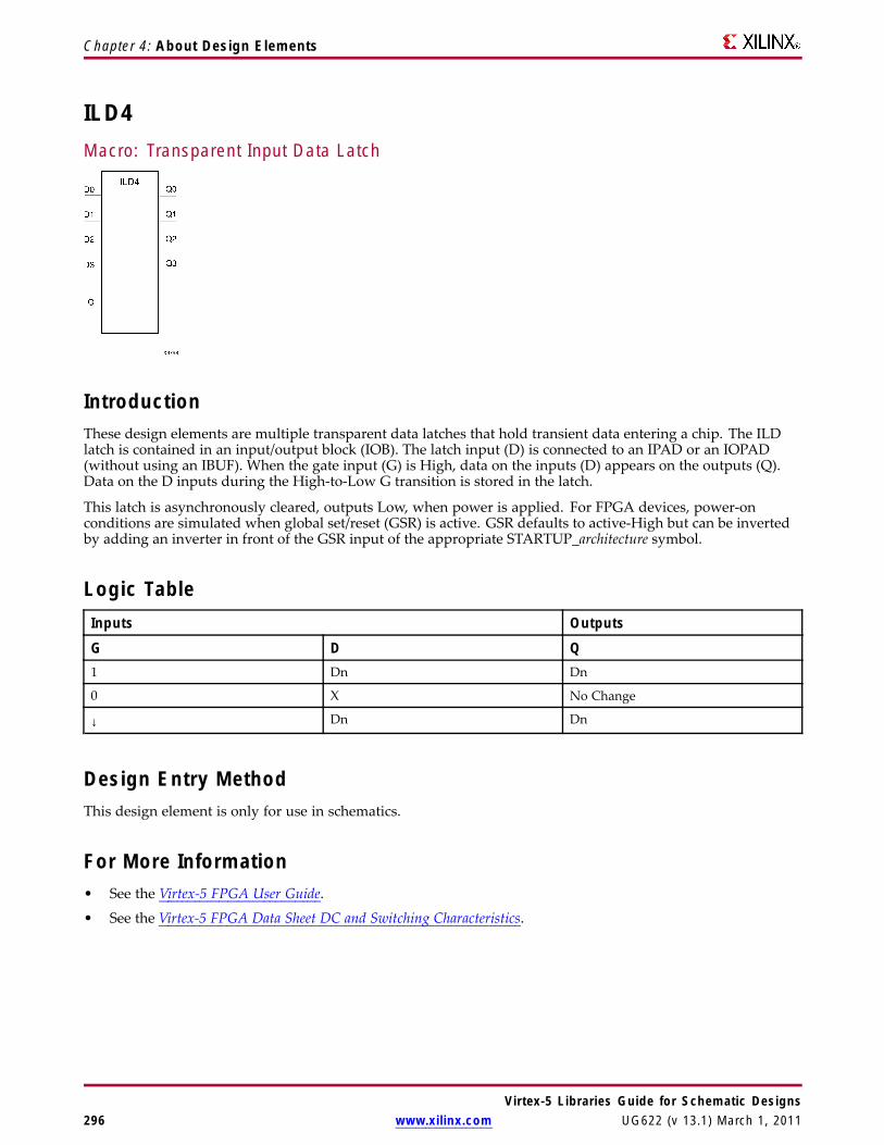
Chapter 4: About Design Elements
ILD4Macro: Transparent Input Data Latch
IntroductionThese design elements are multiple transparent data latches that hold transient data entering a chip. The ILDlatch is contained in an input/output block (IOB). The latch input (D) is connected to an IPAD or an IOPAD(without using an IBUF). When the gate input (G) is High, data on the inputs (D) appears on the outputs (Q).Data on the D inputs during the High-to-Low G transition is stored in the latch.
This latch is asynchronously cleared, outputs Low, when power is applied. For FPGA devices, power-onconditions are simulated when global set/reset (GSR) is active. GSR defaults to active-High but can be invertedby adding an inverter in front of the GSR input of the appropriate STARTUP_architecture symbol.
Logic TableInputs Outputs
G D Q1 Dn Dn
0 X No Change
↓ Dn Dn
Design Entry MethodThis design element is only for use in schematics.
For More Information• See the Virtex-5 FPGA User Guide.
• See the Virtex-5 FPGA Data Sheet DC and Switching Characteristics.
Virtex-5 Libraries Guide for Schematic Designs296 www.xilinx.com UG622 (v 13.1) March 1, 2011
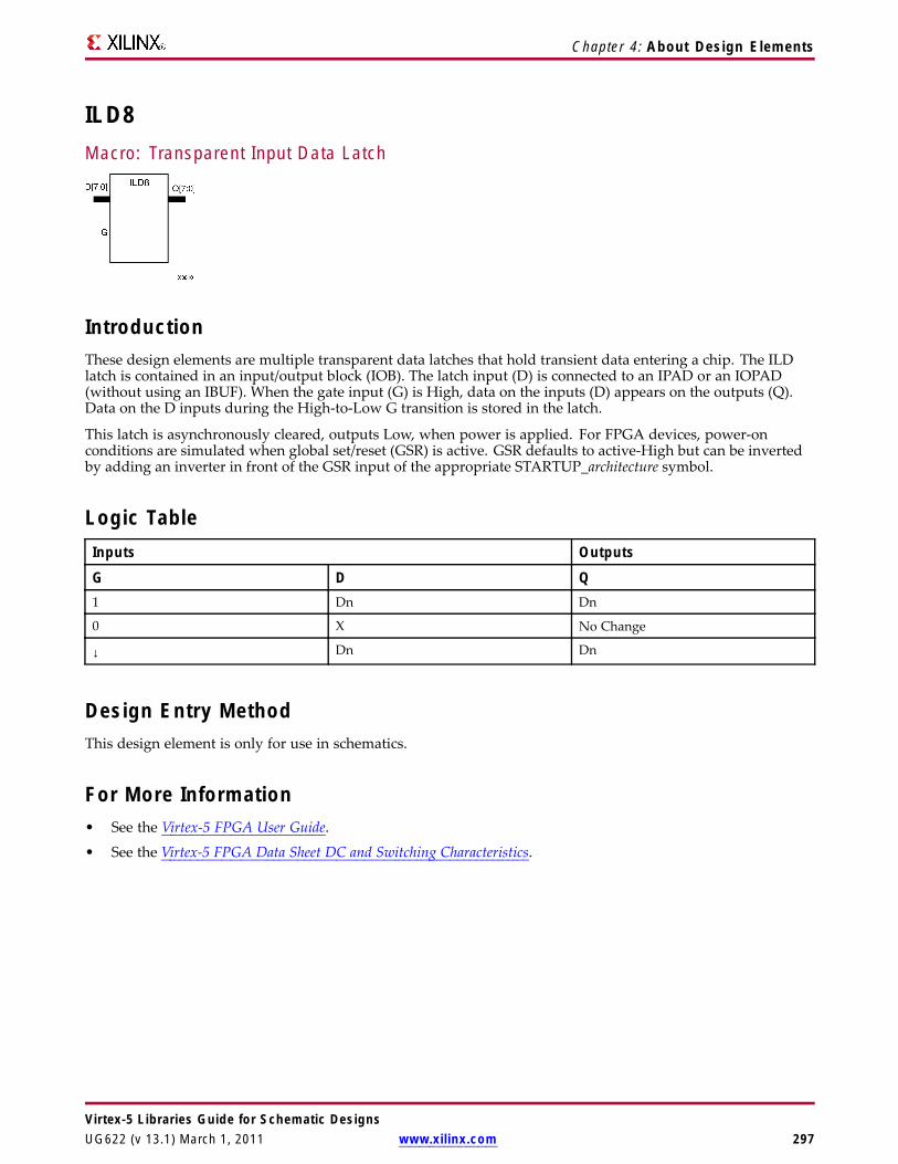
Chapter 4: About Design Elements
ILD8Macro: Transparent Input Data Latch
IntroductionThese design elements are multiple transparent data latches that hold transient data entering a chip. The ILDlatch is contained in an input/output block (IOB). The latch input (D) is connected to an IPAD or an IOPAD(without using an IBUF). When the gate input (G) is High, data on the inputs (D) appears on the outputs (Q).Data on the D inputs during the High-to-Low G transition is stored in the latch.
This latch is asynchronously cleared, outputs Low, when power is applied. For FPGA devices, power-onconditions are simulated when global set/reset (GSR) is active. GSR defaults to active-High but can be invertedby adding an inverter in front of the GSR input of the appropriate STARTUP_architecture symbol.
Logic TableInputs Outputs
G D Q1 Dn Dn
0 X No Change
↓ Dn Dn
Design Entry MethodThis design element is only for use in schematics.
For More Information• See the Virtex-5 FPGA User Guide.
• See the Virtex-5 FPGA Data Sheet DC and Switching Characteristics.
Virtex-5 Libraries Guide for Schematic DesignsUG622 (v 13.1) March 1, 2011 www.xilinx.com 297
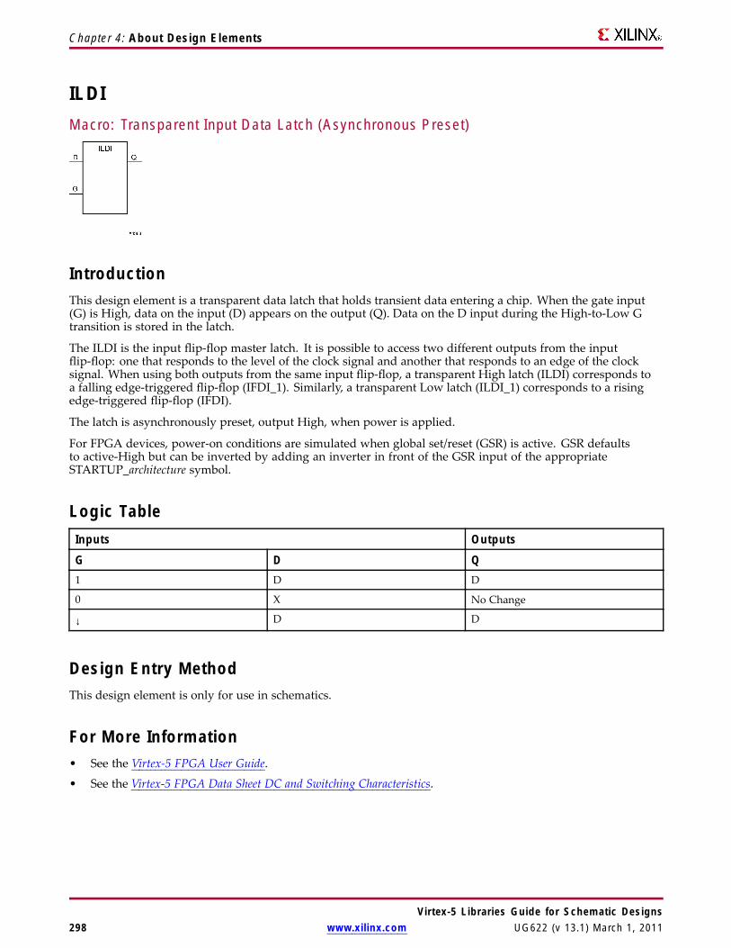
Chapter 4: About Design Elements
ILDIMacro: Transparent Input Data Latch (Asynchronous Preset)
IntroductionThis design element is a transparent data latch that holds transient data entering a chip. When the gate input(G) is High, data on the input (D) appears on the output (Q). Data on the D input during the High-to-Low Gtransition is stored in the latch.
The ILDI is the input flip-flop master latch. It is possible to access two different outputs from the inputflip-flop: one that responds to the level of the clock signal and another that responds to an edge of the clocksignal. When using both outputs from the same input flip-flop, a transparent High latch (ILDI) corresponds toa falling edge-triggered flip-flop (IFDI_1). Similarly, a transparent Low latch (ILDI_1) corresponds to a risingedge-triggered flip-flop (IFDI).
The latch is asynchronously preset, output High, when power is applied.
For FPGA devices, power-on conditions are simulated when global set/reset (GSR) is active. GSR defaultsto active-High but can be inverted by adding an inverter in front of the GSR input of the appropriateSTARTUP_architecture symbol.
Logic TableInputs Outputs
G D Q1 D D
0 X No Change
↓ D D
Design Entry MethodThis design element is only for use in schematics.
For More Information• See the Virtex-5 FPGA User Guide.
• See the Virtex-5 FPGA Data Sheet DC and Switching Characteristics.
Virtex-5 Libraries Guide for Schematic Designs298 www.xilinx.com UG622 (v 13.1) March 1, 2011

Chapter 4: About Design Elements
ILDI_1Macro: Transparent Input Data Latch with Inverted Gate (Asynchronous Preset)
IntroductionThis design element is a transparent data latch that holds transient data entering a chip. When the gate input(G) is Low, data on the data input (D) appears on the data output (Q). Data on D during the Low-to-High Gtransition is stored in the latch.
The latch is asynchronously preset, output High, when power is applied.
For FPGA devices, power-on conditions are simulated when global set/reset (GSR) is active. GSR defaultsto active-High but can be inverted by adding an inverter in front of the GSR input of the appropriateSTARTUP_architecture symbol.
Logic TableInputs Outputs
G D Q0 1 1
0 0 0
1 X No Change
↑ D D
Design Entry MethodThis design element is only for use in schematics.
For More Information• See the Virtex-5 FPGA User Guide.
• See the Virtex-5 FPGA Data Sheet DC and Switching Characteristics.
Virtex-5 Libraries Guide for Schematic DesignsUG622 (v 13.1) March 1, 2011 www.xilinx.com 299
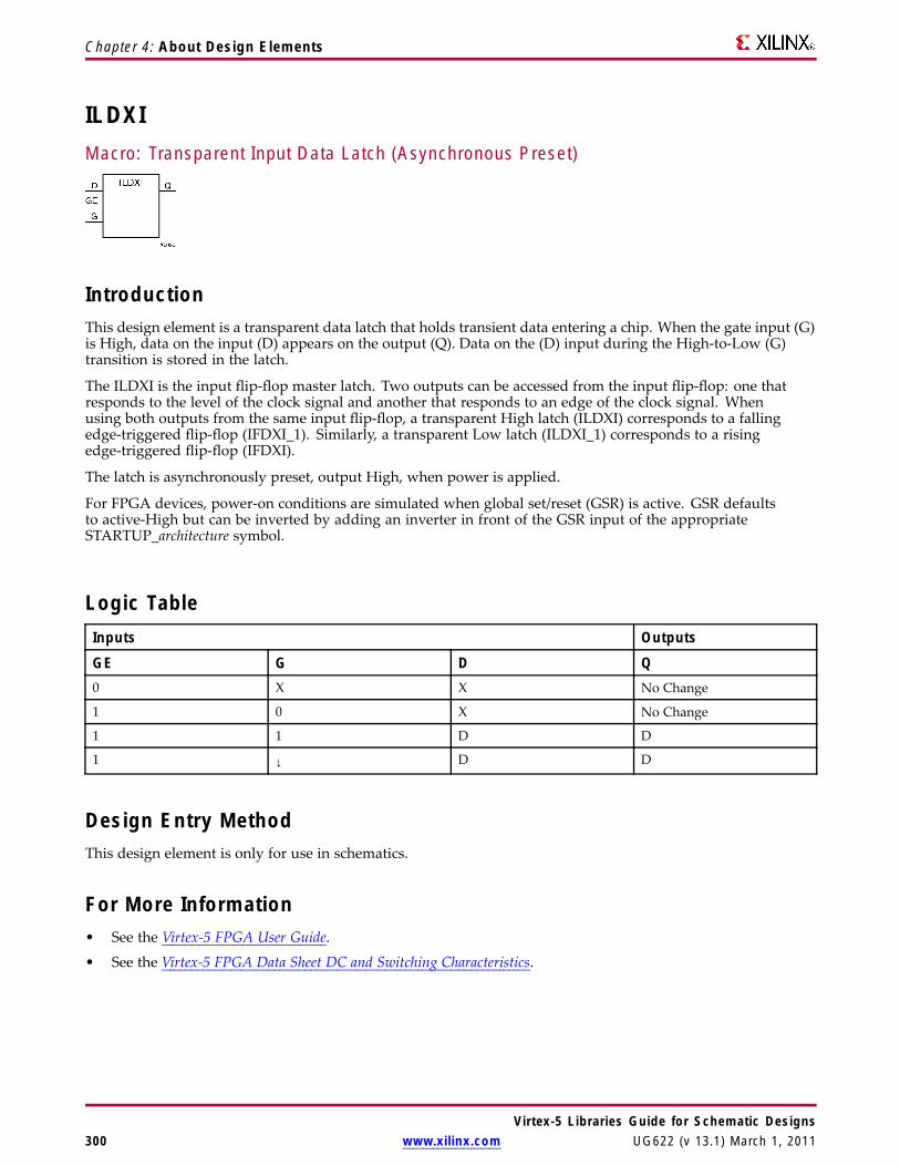
Chapter 4: About Design Elements
ILDXIMacro: Transparent Input Data Latch (Asynchronous Preset)
IntroductionThis design element is a transparent data latch that holds transient data entering a chip. When the gate input (G)is High, data on the input (D) appears on the output (Q). Data on the (D) input during the High-to-Low (G)transition is stored in the latch.
The ILDXI is the input flip-flop master latch. Two outputs can be accessed from the input flip-flop: one thatresponds to the level of the clock signal and another that responds to an edge of the clock signal. Whenusing both outputs from the same input flip-flop, a transparent High latch (ILDXI) corresponds to a fallingedge-triggered flip-flop (IFDXI_1). Similarly, a transparent Low latch (ILDXI_1) corresponds to a risingedge-triggered flip-flop (IFDXI).
The latch is asynchronously preset, output High, when power is applied.
For FPGA devices, power-on conditions are simulated when global set/reset (GSR) is active. GSR defaultsto active-High but can be inverted by adding an inverter in front of the GSR input of the appropriateSTARTUP_architecture symbol.
Logic TableInputs Outputs
GE G D Q0 X X No Change
1 0 X No Change
1 1 D D
1 ↓ D D
Design Entry MethodThis design element is only for use in schematics.
For More Information• See the Virtex-5 FPGA User Guide.
• See the Virtex-5 FPGA Data Sheet DC and Switching Characteristics.
Virtex-5 Libraries Guide for Schematic Designs300 www.xilinx.com UG622 (v 13.1) March 1, 2011

Chapter 4: About Design Elements
ILDXI_1Macro: Transparent Input Data Latch with Inverted Gate (Asynchronous Preset)
IntroductionThis design element is a transparent data latch that holds transient data entering a chip.
The latch is asynchronously preset, output High, when power is applied.
For FPGA devices, power-on conditions are simulated when global set/reset (GSR) is active. GSR defaultsto active-High but can be inverted by adding an inverter in front of the GSR input of the appropriateSTARTUP_architecture symbol.
Logic TableInputs Outputs
GE G D Q0 X X No Change
1 1 X No Change
1 0 D D
1 ↑ D D
Design Entry MethodThis design element is only for use in schematics.
For More Information• See the Virtex-5 FPGA User Guide.
• See the Virtex-5 FPGA Data Sheet DC and Switching Characteristics.
Virtex-5 Libraries Guide for Schematic DesignsUG622 (v 13.1) March 1, 2011 www.xilinx.com 301
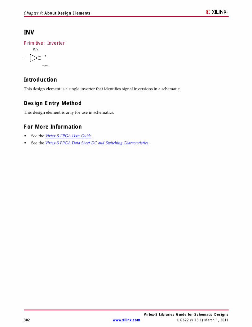
Chapter 4: About Design Elements
INVPrimitive: Inverter
IntroductionThis design element is a single inverter that identifies signal inversions in a schematic.
Design Entry MethodThis design element is only for use in schematics.
For More Information• See the Virtex-5 FPGA User Guide.
• See the Virtex-5 FPGA Data Sheet DC and Switching Characteristics.
Virtex-5 Libraries Guide for Schematic Designs302 www.xilinx.com UG622 (v 13.1) March 1, 2011

Chapter 4: About Design Elements
INV16Macro: 16 Inverters
IntroductionThis design element is a multiple inverter that identifies signal inversions in a schematic.
Design Entry MethodThis design element is only for use in schematics.
For More Information• See the Virtex-5 FPGA User Guide.
• See the Virtex-5 FPGA Data Sheet DC and Switching Characteristics.
Virtex-5 Libraries Guide for Schematic DesignsUG622 (v 13.1) March 1, 2011 www.xilinx.com 303

Chapter 4: About Design Elements
INV4Macro: Four Inverters
IntroductionThis design element is a multiple inverter that identifies signal inversions in a schematic.
Design Entry MethodThis design element is only for use in schematics.
For More Information• See the Virtex-5 FPGA User Guide.
• See the Virtex-5 FPGA Data Sheet DC and Switching Characteristics.
Virtex-5 Libraries Guide for Schematic Designs304 www.xilinx.com UG622 (v 13.1) March 1, 2011
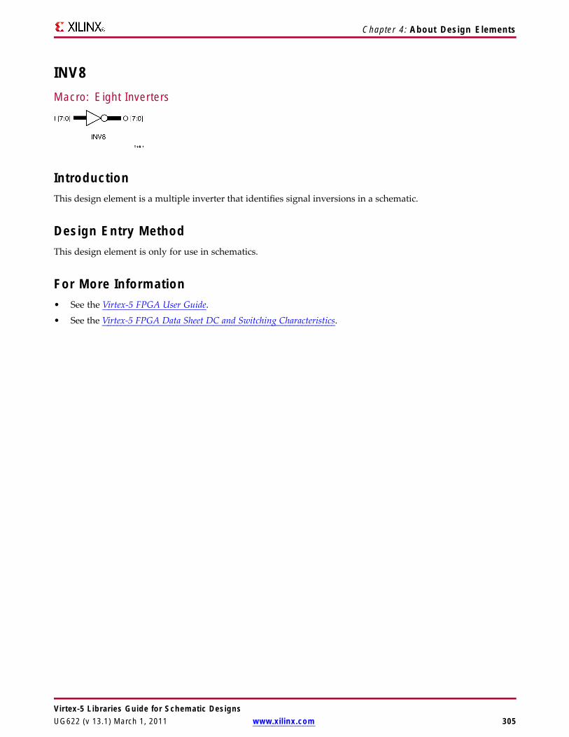
Chapter 4: About Design Elements
INV8Macro: Eight Inverters
IntroductionThis design element is a multiple inverter that identifies signal inversions in a schematic.
Design Entry MethodThis design element is only for use in schematics.
For More Information• See the Virtex-5 FPGA User Guide.
• See the Virtex-5 FPGA Data Sheet DC and Switching Characteristics.
Virtex-5 Libraries Guide for Schematic DesignsUG622 (v 13.1) March 1, 2011 www.xilinx.com 305

Chapter 4: About Design Elements
IOBUFPrimitive: Bi-Directional Buffer
IntroductionThe design element is a bidirectional single-ended I/O Buffer used to connect internal logic to an externalbidirectional pin.
Logic TableInputs Bidirectional Outputs
T I IO O1 X Z IO
0 1 1 1
0 0 0 0
Port DescriptionsPort Direction Width FunctionO Output 1 Buffer output
IO Inout 1 Buffer inout
I Input 1 Buffer input
T Input 1 3-State enable input
Design Entry MethodThis design element can be used in schematics.
Available AttributesAttribute Type Allowed Values Default DescriptionDRIVE Integer 2, 4, 6, 8, 12, 16, 24 12 Selects output drive strength (mA)
for the SelectIO™ buffers that usethe LVTTL, LVCMOS12, LVCMOS15,LVCMOS18, LVCMOS25, or LVCMOS33interface I/O standard.
IOSTANDARD String See Data Sheet "DEFAULT" Assigns an I/O standard to the element.
SLEW String "SLOW", "FAST","QUIETIO"
"SLOW" Sets the output rise and fall time. See theData Sheet for recommendations of thebest setting for this attribute.
Virtex-5 Libraries Guide for Schematic Designs306 www.xilinx.com UG622 (v 13.1) March 1, 2011

Chapter 4: About Design Elements
For More Information• See the Virtex-5 FPGA User Guide.
• See the Virtex-5 FPGA Data Sheet DC and Switching Characteristics.
Virtex-5 Libraries Guide for Schematic DesignsUG622 (v 13.1) March 1, 2011 www.xilinx.com 307

Chapter 4: About Design Elements
IOBUFDSPrimitive: 3-State Differential Signaling I/O Buffer with Active Low Output Enable
IntroductionThe design element is a bidirectional buffer that supports low-voltage, differential signaling. For the IOBUFDS, adesign level interface signal is represented as two distinct ports (IO and IOB), one deemed the "master" andthe other the "slave." The master and the slave are opposite phases of the same logical signal (for example,MYNET_P and MYNET_N). Optionally, a programmable differential termination feature is available to helpimprove signal integrity and reduce external components. Also available is a programmable delay is to assist inthe capturing of incoming data to the device.
Logic TableInputs Bidirectional Outputs
I T IO IOB OX 1 Z Z No Change
0 0 0 1 0
I 0 1 0 1
Port DescriptionsPort Direction Width FunctionO Output 1 Buffer output
IO Inout 1 Diff_p inout
IOB Inout 1 Diff_n inout
I Input 1 Buffer input
T Input 1 3-state enable input
Design Entry MethodThis design element can be used in schematics.
Available AttributesAttribute Type Allowed Values Default DescriptionIOSTANDARD String See Data Sheet "DEFAULT" Assigns an I/O standard to the element.
Virtex-5 Libraries Guide for Schematic Designs308 www.xilinx.com UG622 (v 13.1) March 1, 2011

Chapter 4: About Design Elements
For More Information• See the Virtex-5 FPGA User Guide.
• See the Virtex-5 FPGA Data Sheet DC and Switching Characteristics.
Virtex-5 Libraries Guide for Schematic DesignsUG622 (v 13.1) March 1, 2011 www.xilinx.com 309

Chapter 4: About Design Elements
IODELAYPrimitive: Input and Output Fixed or Variable Delay Element
IntroductionThis design element can be used to provide a fixed delay or an adjustable delay to the input path and a fixeddelay for the output path of the FPGA. This delay can be useful for the purpose of data alignment of incoming oroutgoing data to/from the chip, as well as allowing for the tracking of data alignment over process, temperature,and voltage (PVT). The IODELAY is available on all FPGA I/Os and, when used in conjunction with theIDELAYCTRL component circuitry, can provide precise time increments of delay. When used in variable mode,the input path can be adjusted for increasing and decreasing amounts of delay. The output delay path is onlyavailable in a fixed delay. The IODELAY can also be used to add additional static or variable delay to an internalpath (within the FPGA fabric). However, when IODELAY is used that way, this device is no longer available tothe associated I/O for input or output path delays.
Port DescriptionsPort Direction Width FunctionDATAOUT Output 1 Delayed data output from input port (connect to input
datapath logic)
IDATAIN Input 1 Data input to device from the I/O (connect directly to port,I/O Buffer). When IDATAIN is used, DATAIN must be tiedto a logic zero (ground).
ODATAIN Input 1 Data input for the output datapath from the device (connectto output data source). When ODATAIN is used, DATAINmust be tied to a logic zero (ground).
DATAIN Input 1 Data input for the internal datapath delay. When DATAINis used, IDATAIN and ODATAIN must be tied to a logiczero (ground).
T Input 1 3-state input control. Tie high for input-only or internaldelay or tie low for output only.
CE Input 1 Active high enable increment/decrement function
INC Input 1 Increment / Decrement tap delay
C Input 1 Clock input (Must be connected for variable mode)
RST Input 1 Active high, synchronous reset, resets delay chain toIDELAY_VALUE/ ODELAY_VALUE tap. If no value isspecified, the default is 0.
Design Entry MethodThis design element can be used in schematics.
Virtex-5 Libraries Guide for Schematic Designs310 www.xilinx.com UG622 (v 13.1) March 1, 2011
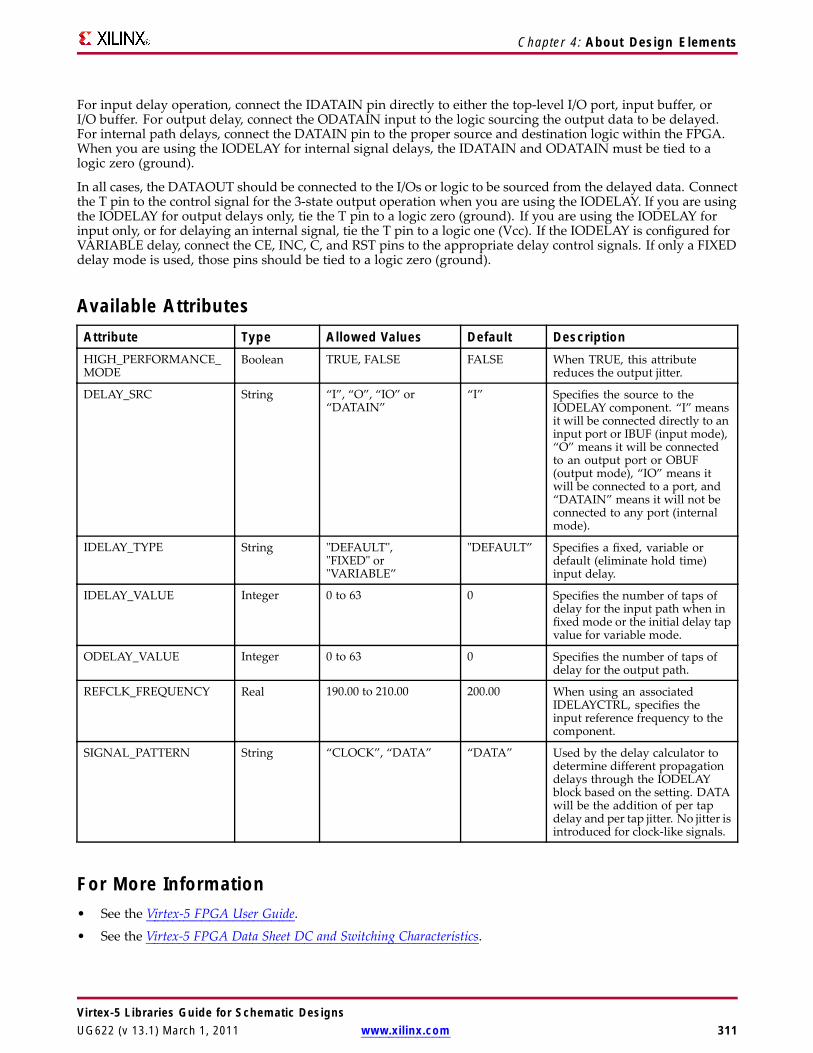
Chapter 4: About Design Elements
For input delay operation, connect the IDATAIN pin directly to either the top-level I/O port, input buffer, orI/O buffer. For output delay, connect the ODATAIN input to the logic sourcing the output data to be delayed.For internal path delays, connect the DATAIN pin to the proper source and destination logic within the FPGA.When you are using the IODELAY for internal signal delays, the IDATAIN and ODATAIN must be tied to alogic zero (ground).
In all cases, the DATAOUT should be connected to the I/Os or logic to be sourced from the delayed data. Connectthe T pin to the control signal for the 3-state output operation when you are using the IODELAY. If you are usingthe IODELAY for output delays only, tie the T pin to a logic zero (ground). If you are using the IODELAY forinput only, or for delaying an internal signal, tie the T pin to a logic one (Vcc). If the IODELAY is configured forVARIABLE delay, connect the CE, INC, C, and RST pins to the appropriate delay control signals. If only a FIXEDdelay mode is used, those pins should be tied to a logic zero (ground).
Available AttributesAttribute Type Allowed Values Default DescriptionHIGH_PERFORMANCE_MODE
Boolean TRUE, FALSE FALSE When TRUE, this attributereduces the output jitter.
DELAY_SRC String “I”, “O”, “IO” or“DATAIN”
“I” Specifies the source to theIODELAY component. “I” meansit will be connected directly to aninput port or IBUF (input mode),“O” means it will be connectedto an output port or OBUF(output mode), “IO” means itwill be connected to a port, and“DATAIN” means it will not beconnected to any port (internalmode).
IDELAY_TYPE String "DEFAULT","FIXED" or"VARIABLE”
"DEFAULT” Specifies a fixed, variable ordefault (eliminate hold time)input delay.
IDELAY_VALUE Integer 0 to 63 0 Specifies the number of taps ofdelay for the input path when infixed mode or the initial delay tapvalue for variable mode.
ODELAY_VALUE Integer 0 to 63 0 Specifies the number of taps ofdelay for the output path.
REFCLK_FREQUENCY Real 190.00 to 210.00 200.00 When using an associatedIDELAYCTRL, specifies theinput reference frequency to thecomponent.
SIGNAL_PATTERN String “CLOCK”, “DATA” “DATA” Used by the delay calculator todetermine different propagationdelays through the IODELAYblock based on the setting. DATAwill be the addition of per tapdelay and per tap jitter. No jitter isintroduced for clock-like signals.
For More Information• See the Virtex-5 FPGA User Guide.
• See the Virtex-5 FPGA Data Sheet DC and Switching Characteristics.
Virtex-5 Libraries Guide for Schematic DesignsUG622 (v 13.1) March 1, 2011 www.xilinx.com 311
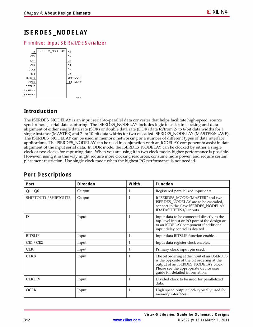
Chapter 4: About Design Elements
ISERDES_NODELAYPrimitive: Input SERial/DESerializer
IntroductionThe ISERDES_NODELAY is an input serial-to-parallel data converter that helps facilitate high-speed, sourcesynchronous, serial data capturing. The ISERDES_NODELAY includes logic to assist in clocking and dataalignment of either single data rate (SDR) or double data rate (DDR) data to/from 2- to 6-bit data widths for asingle instance (MASTER) and 7- to 10-bit data widths for two cascaded ISERDES_NODELAY (MASTER/SLAVE).The ISERDES_NODELAY can be used in memory, networking or a number of different types of data interfaceapplications. The ISERDES_NODELAY can be used in conjunction with an IODELAY component to assist in dataalignment of the input serial data. In DDR mode, the ISERDES_NODELAY can be clocked by either a singleclock or two clocks for capturing data. When you are using it in two clock mode, higher performance is possible.However, using it in this way might require more clocking resources, consume more power, and require certainplacement restriction. Use single clock mode when the highest I/O performance is not needed.
Port DescriptionsPort Direction Width FunctionQ1 - Q6 Output 1 Registered parallelized input data.
SHIFTOUT1 / SHIFTOUT2 Output 1 If ISERDES_MODE="MASTER" and twoISERDES_NODELAY are to be cascaded,connect to the slave ISERDES_NODELAYIDATASHIFTIN1/2 inputs.
D Input 1 Input data to be connected directly to thetop-level input or I/O port of the design orto an IODELAY component if additionalinput delay control is desired.
BITSLIP Input 1 Input data BITSLIP function enable.
CE1 / CE2 Input 1 Input data register clock enables.
CLK Input 1 Primary clock input pin used.
CLKB Input 1 The bit ordering at the input of anOSERDESis the opposite of the bit ordering at theoutput of an ISERDES_NODELAY block.Please see the appropriate device userguide for detailed information.
CLKDIV Input 1 Divided clock to be used for parallelizeddata.
OCLK Input 1 High speed output clock typically used formemory interfaces.
Virtex-5 Libraries Guide for Schematic Designs312 www.xilinx.com UG622 (v 13.1) March 1, 2011
Chapter 4: About Design Elements
Port Direction Width FunctionSHIFTIN1 / SHIFTIN2 Input 1 If ISERDES_MODE="SLAVE" connect
to the master ISERDES_NODELAYIDATASHIFTOUT1/2 outputs. This pinmust be grounded.
RST Input 1 Active high asynchronous reset signal forthe registers of the SERDES.
Design Entry MethodThis design element can be used in schematics.
Available AttributesAttribute Type Allowed Values Default DescriptionBITSLIP_ENABLE Boolean TRUE or FALSE FALSE Enable the BITSLIP functionality. Only
available in NETWORKING mode.
DATA_RATE String "SDR" or "DDR" "DDR" Single Data Rate or Double Data Rateoperation
DATA_WIDTH Integer 4,6,8 or 10 ifDATA_RATE="DDR",2,3,4,5,6,7 or 8 ifDATA_RATE="SDR"
4 Parallel data width selection
INTERFACE_TYPE String "MEMORY" or"NETWORKING”
"MEMORY" Memory or Networking interface type
SERDES_MODE String "MASTER" or"SLAVE"
"MASTER" Specify whether the ISERDES is operatingin master or slave modes when cascadedwidth expansion.
NUM_CE Integer 1 or 2 2 Specifies the number of clock enablesused for the ISERDES_NODELAY.
For More Information• See the Virtex-5 FPGA User Guide.
• See the Virtex-5 FPGA Data Sheet DC and Switching Characteristics.
Virtex-5 Libraries Guide for Schematic DesignsUG622 (v 13.1) March 1, 2011 www.xilinx.com 313

Chapter 4: About Design Elements
JTAGPPC440Primitive: JTAG Primitive for the Power PC
IntroductionThis design element connects the JTAG logic in the PPC440 core to the JTAG logic of the FPGA device in whichthe core resides. The connections are made through programmable routing, so the connection only existsafter configuration.
Port DescriptionsInputs OutputsTDOPPC TCK
TDIPPC
TMS
Design Entry MethodThis design element is only for use in schematics.
For More Information• See the Virtex-5 FPGA User Guide.
• See the Virtex-5 FPGA Data Sheet DC and Switching Characteristics.
Virtex-5 Libraries Guide for Schematic Designs314 www.xilinx.com UG622 (v 13.1) March 1, 2011

Chapter 4: About Design Elements
KEEPERPrimitive: KEEPER Symbol
IntroductionThe design element is a weak keeper element that retains the value of the net connected to its bidirectional O pin.For example, if a logic 1 is being driven onto the net, KEEPER drives a weak/resistive 1 onto the net. If the netdriver is then 3-stated, KEEPER continues to drive a weak/resistive 1 onto the net.
Port DescriptionsName Direction Width FunctionO Output 1-Bit Keeper output
Design Entry MethodThis design element can be used in schematics or instantiated in HDL code. Instantiation templates for VHDLand Verilog are available below.
This element can be connected to a net in the following locations on a top-level schematic file:
• A net connected to an input IO Marker
• A net connected to both an output IO Marker and 3-statable IO element, such as an OBUFT.
For More Information• See the Virtex-5 FPGA User Guide.
• See the Virtex-5 FPGA Data Sheet DC and Switching Characteristics.
Virtex-5 Libraries Guide for Schematic DesignsUG622 (v 13.1) March 1, 2011 www.xilinx.com 315

Chapter 4: About Design Elements
KEY_CLEARPrimitive: Virtex-5 Configuration Encryption Key Erase
IntroductionThis design element allows you to erase the configuration encryption circuit key register from internal logic.
Port DescriptionsPort Direction Width FunctionKEYCLEARB Input 1 Active low input, clears the
configuration encryptionkey
Design Entry MethodThis design element can be used in schematics.
For More Information• See the Virtex-5 FPGA User Guide.
• See the Virtex-5 FPGA Data Sheet DC and Switching Characteristics.
Virtex-5 Libraries Guide for Schematic Designs316 www.xilinx.com UG622 (v 13.1) March 1, 2011
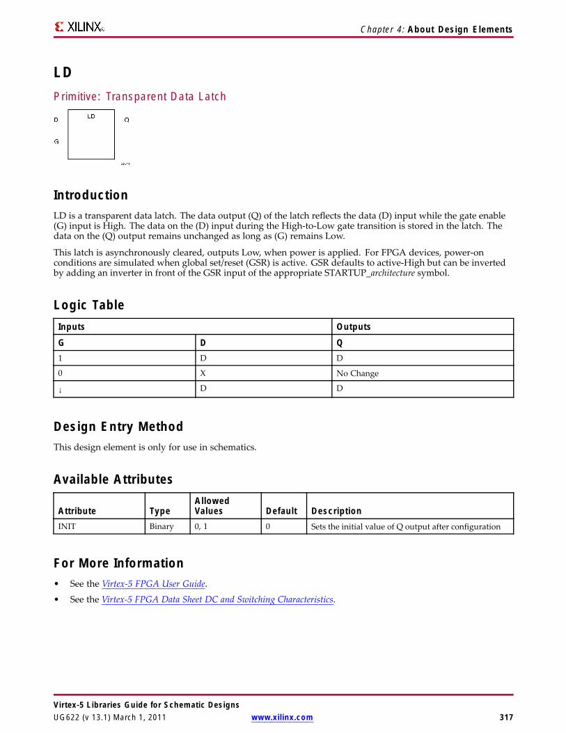
Chapter 4: About Design Elements
LDPrimitive: Transparent Data Latch
IntroductionLD is a transparent data latch. The data output (Q) of the latch reflects the data (D) input while the gate enable(G) input is High. The data on the (D) input during the High-to-Low gate transition is stored in the latch. Thedata on the (Q) output remains unchanged as long as (G) remains Low.
This latch is asynchronously cleared, outputs Low, when power is applied. For FPGA devices, power-onconditions are simulated when global set/reset (GSR) is active. GSR defaults to active-High but can be invertedby adding an inverter in front of the GSR input of the appropriate STARTUP_architecture symbol.
Logic TableInputs Outputs
G D Q1 D D
0 X No Change
↓ D D
Design Entry MethodThis design element is only for use in schematics.
Available Attributes
Attribute TypeAllowedValues Default Description
INIT Binary 0, 1 0 Sets the initial value of Q output after configuration
For More Information• See the Virtex-5 FPGA User Guide.
• See the Virtex-5 FPGA Data Sheet DC and Switching Characteristics.
Virtex-5 Libraries Guide for Schematic DesignsUG622 (v 13.1) March 1, 2011 www.xilinx.com 317

Chapter 4: About Design Elements
LD_1Primitive: Transparent Data Latch with Inverted Gate
IntroductionThis design element is a transparent data latch with an inverted gate. The data output (Q) of the latch reflects thedata (D) input while the gate enable (G) input is Low. The data on the (D) input during the Low-to-High gatetransition is stored in the latch. The data on the (Q) output remains unchanged as long as (G) remains High.
This latch is asynchronously cleared, outputs Low, when power is applied. For FPGA devices, power-onconditions are simulated when global set/reset (GSR) is active. GSR defaults to active-High but can be invertedby adding an inverter in front of the GSR input of the appropriate STARTUP_architecture symbol.
Logic TableInputs Outputs
G D Q0 D D
1 X No Change
↑ D D
Design Entry MethodThis design element is only for use in schematics.
Available Attributes
Attribute TypeAllowedValues Default Description
INIT Binary 0, 1 0 Sets the initial value of Q output after configuration.
For More Information• See the Virtex-5 FPGA User Guide.
• See the Virtex-5 FPGA Data Sheet DC and Switching Characteristics.
Virtex-5 Libraries Guide for Schematic Designs318 www.xilinx.com UG622 (v 13.1) March 1, 2011

Chapter 4: About Design Elements
LD16Macro: Multiple Transparent Data Latch
IntroductionThis design element has 16 transparent data latches with a common gate enable (G). The data output (Q) of thelatch reflects the data (D) input while the gate enable (G) input is High. The data on the (D) input during theHigh-to-Low gate transition is stored in the latch. The data on the (Q) output remains unchanged as long as(G) remains Low.
This latch is asynchronously cleared, outputs Low, when power is applied. For FPGA devices, power-onconditions are simulated when global set/reset (GSR) is active. GSR defaults to active-High but can be invertedby adding an inverter in front of the GSR input of the appropriate STARTUP_architecture symbol.
Logic TableInputs Outputs
G D Q1 Dn Dn
0 X No Change
↓ Dn Dn
Design Entry MethodThis design element is only for use in schematics.
Available Attributes
Attribute TypeAllowedValues Default Description
INIT Binary Any 16-Bit Value All zeros Sets the initial value of Q output afterconfiguration
For More Information• See the Virtex-5 FPGA User Guide.
• See the Virtex-5 FPGA Data Sheet DC and Switching Characteristics.
Virtex-5 Libraries Guide for Schematic DesignsUG622 (v 13.1) March 1, 2011 www.xilinx.com 319
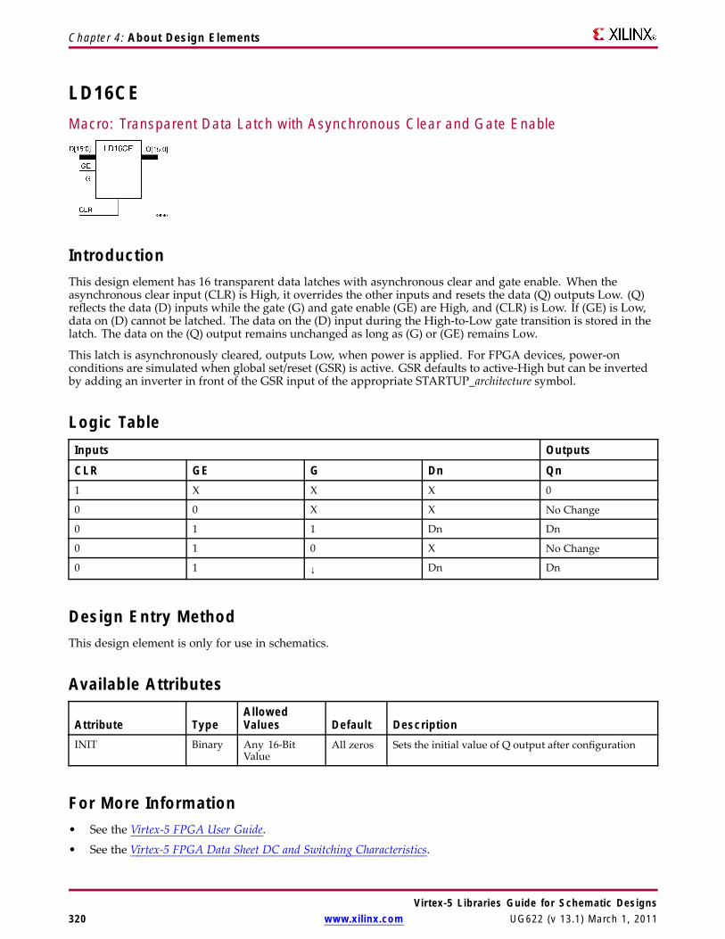
Chapter 4: About Design Elements
LD16CEMacro: Transparent Data Latch with Asynchronous Clear and Gate Enable
IntroductionThis design element has 16 transparent data latches with asynchronous clear and gate enable. When theasynchronous clear input (CLR) is High, it overrides the other inputs and resets the data (Q) outputs Low. (Q)reflects the data (D) inputs while the gate (G) and gate enable (GE) are High, and (CLR) is Low. If (GE) is Low,data on (D) cannot be latched. The data on the (D) input during the High-to-Low gate transition is stored in thelatch. The data on the (Q) output remains unchanged as long as (G) or (GE) remains Low.
This latch is asynchronously cleared, outputs Low, when power is applied. For FPGA devices, power-onconditions are simulated when global set/reset (GSR) is active. GSR defaults to active-High but can be invertedby adding an inverter in front of the GSR input of the appropriate STARTUP_architecture symbol.
Logic TableInputs Outputs
CLR GE G Dn Qn1 X X X 0
0 0 X X No Change
0 1 1 Dn Dn
0 1 0 X No Change
0 1 ↓ Dn Dn
Design Entry MethodThis design element is only for use in schematics.
Available Attributes
Attribute TypeAllowedValues Default Description
INIT Binary Any 16-BitValue
All zeros Sets the initial value of Q output after configuration
For More Information• See the Virtex-5 FPGA User Guide.
• See the Virtex-5 FPGA Data Sheet DC and Switching Characteristics.
Virtex-5 Libraries Guide for Schematic Designs320 www.xilinx.com UG622 (v 13.1) March 1, 2011
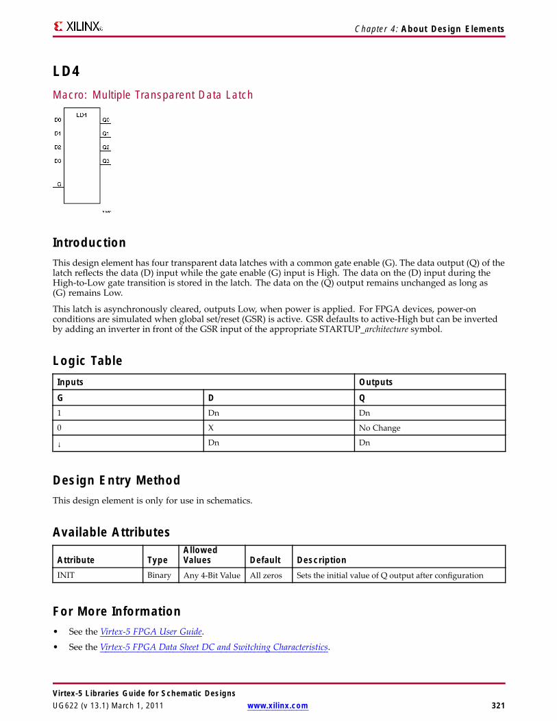
Chapter 4: About Design Elements
LD4Macro: Multiple Transparent Data Latch
IntroductionThis design element has four transparent data latches with a common gate enable (G). The data output (Q) of thelatch reflects the data (D) input while the gate enable (G) input is High. The data on the (D) input during theHigh-to-Low gate transition is stored in the latch. The data on the (Q) output remains unchanged as long as(G) remains Low.
This latch is asynchronously cleared, outputs Low, when power is applied. For FPGA devices, power-onconditions are simulated when global set/reset (GSR) is active. GSR defaults to active-High but can be invertedby adding an inverter in front of the GSR input of the appropriate STARTUP_architecture symbol.
Logic TableInputs Outputs
G D Q1 Dn Dn
0 X No Change
↓ Dn Dn
Design Entry MethodThis design element is only for use in schematics.
Available Attributes
Attribute TypeAllowedValues Default Description
INIT Binary Any 4-Bit Value All zeros Sets the initial value of Q output after configuration
For More Information• See the Virtex-5 FPGA User Guide.
• See the Virtex-5 FPGA Data Sheet DC and Switching Characteristics.
Virtex-5 Libraries Guide for Schematic DesignsUG622 (v 13.1) March 1, 2011 www.xilinx.com 321

Chapter 4: About Design Elements
LD4CEMacro: Transparent Data Latch with Asynchronous Clear and Gate Enable
IntroductionThis design element has 4 transparent data latches with asynchronous clear and gate enable. When theasynchronous clear input (CLR) is High, it overrides the other inputs and resets the data (Q) outputs Low. (Q)reflects the data (D) inputs while the gate (G) and gate enable (GE) are High, and (CLR) is Low. If (GE) is Low,data on (D) cannot be latched. The data on the (D) input during the High-to-Low gate transition is stored in thelatch. The data on the (Q) output remains unchanged as long as (G) or (GE) remains Low.
This latch is asynchronously cleared, outputs Low, when power is applied. For FPGA devices, power-onconditions are simulated when global set/reset (GSR) is active. GSR defaults to active-High but can be invertedby adding an inverter in front of the GSR input of the appropriate STARTUP_architecture symbol.
Logic TableInputs Outputs
CLR GE G Dn Qn1 X X X 0
0 0 X X No Change
0 1 1 Dn Dn
0 1 0 X No Change
0 1 ↓ Dn Dn
Design Entry MethodThis design element is only for use in schematics.
Available Attributes
Attribute TypeAllowedValues Default Description
INIT Binary Any 4-BitValue
All zeros Sets the initial value of Q output afterconfiguration
For More Information• See the Virtex-5 FPGA User Guide.• See the Virtex-5 FPGA Data Sheet DC and Switching Characteristics.
Virtex-5 Libraries Guide for Schematic Designs322 www.xilinx.com UG622 (v 13.1) March 1, 2011

Chapter 4: About Design Elements
LD8Macro: Multiple Transparent Data Latch
IntroductionThis design element has 8 transparent data latches with a common gate enable (G). The data output (Q) of thelatch reflects the data (D) input while the gate enable (G) input is High. The data on the (D) input during theHigh-to-Low gate transition is stored in the latch. The data on the (Q) output remains unchanged as long as(G) remains Low.
This latch is asynchronously cleared, outputs Low, when power is applied. For FPGA devices, power-onconditions are simulated when global set/reset (GSR) is active. GSR defaults to active-High but can be invertedby adding an inverter in front of the GSR input of the appropriate STARTUP_architecture symbol.
Logic TableInputs Outputs
G D Q1 Dn Dn
0 X No Change
↓ Dn Dn
Design Entry MethodThis design element is only for use in schematics.
Available AttributesAttribute Type Allowed Values Default DescriptionINIT Binary Any 8-Bit Value All zeros Sets the initial value of Q output after configuration
For More Information• See the Virtex-5 FPGA User Guide.
• See the Virtex-5 FPGA Data Sheet DC and Switching Characteristics.
Virtex-5 Libraries Guide for Schematic DesignsUG622 (v 13.1) March 1, 2011 www.xilinx.com 323
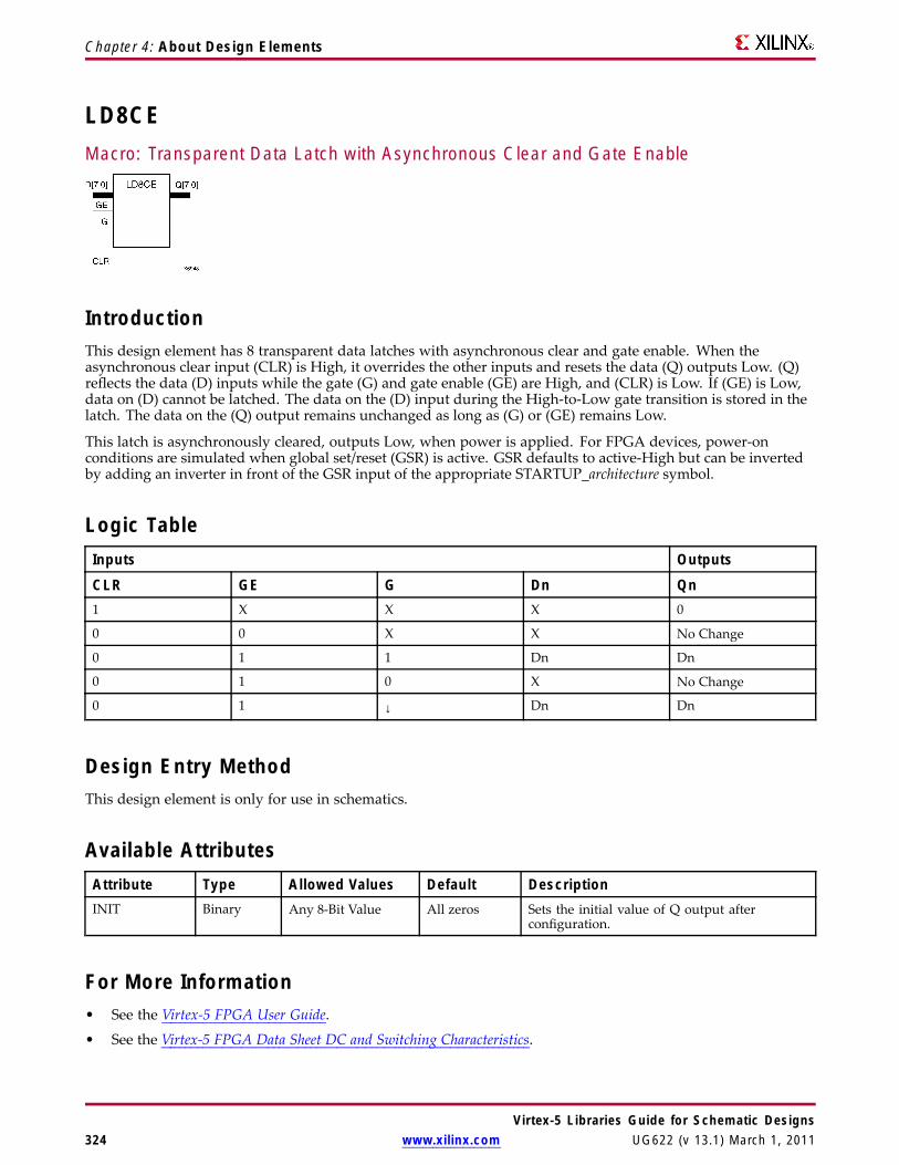
Chapter 4: About Design Elements
LD8CEMacro: Transparent Data Latch with Asynchronous Clear and Gate Enable
IntroductionThis design element has 8 transparent data latches with asynchronous clear and gate enable. When theasynchronous clear input (CLR) is High, it overrides the other inputs and resets the data (Q) outputs Low. (Q)reflects the data (D) inputs while the gate (G) and gate enable (GE) are High, and (CLR) is Low. If (GE) is Low,data on (D) cannot be latched. The data on the (D) input during the High-to-Low gate transition is stored in thelatch. The data on the (Q) output remains unchanged as long as (G) or (GE) remains Low.
This latch is asynchronously cleared, outputs Low, when power is applied. For FPGA devices, power-onconditions are simulated when global set/reset (GSR) is active. GSR defaults to active-High but can be invertedby adding an inverter in front of the GSR input of the appropriate STARTUP_architecture symbol.
Logic TableInputs Outputs
CLR GE G Dn Qn1 X X X 0
0 0 X X No Change
0 1 1 Dn Dn
0 1 0 X No Change
0 1 ↓ Dn Dn
Design Entry MethodThis design element is only for use in schematics.
Available AttributesAttribute Type Allowed Values Default DescriptionINIT Binary Any 8-Bit Value All zeros Sets the initial value of Q output after
configuration.
For More Information• See the Virtex-5 FPGA User Guide.
• See the Virtex-5 FPGA Data Sheet DC and Switching Characteristics.
Virtex-5 Libraries Guide for Schematic Designs324 www.xilinx.com UG622 (v 13.1) March 1, 2011
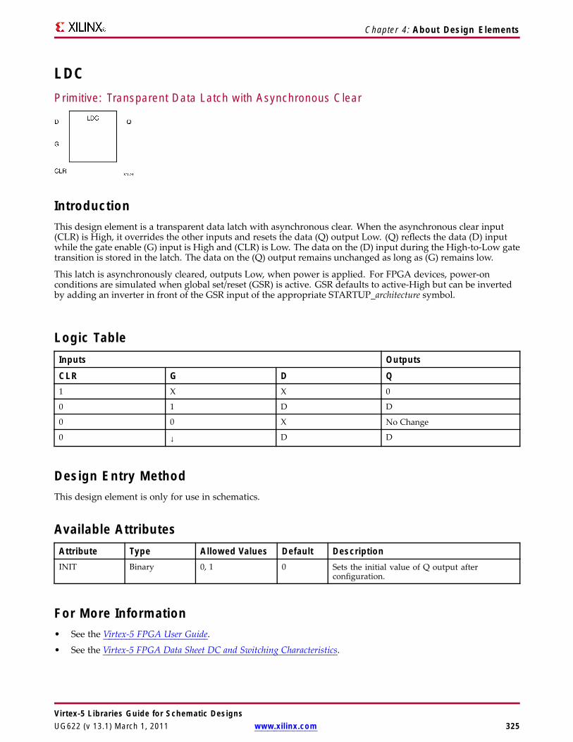
Chapter 4: About Design Elements
LDCPrimitive: Transparent Data Latch with Asynchronous Clear
IntroductionThis design element is a transparent data latch with asynchronous clear. When the asynchronous clear input(CLR) is High, it overrides the other inputs and resets the data (Q) output Low. (Q) reflects the data (D) inputwhile the gate enable (G) input is High and (CLR) is Low. The data on the (D) input during the High-to-Low gatetransition is stored in the latch. The data on the (Q) output remains unchanged as long as (G) remains low.
This latch is asynchronously cleared, outputs Low, when power is applied. For FPGA devices, power-onconditions are simulated when global set/reset (GSR) is active. GSR defaults to active-High but can be invertedby adding an inverter in front of the GSR input of the appropriate STARTUP_architecture symbol.
Logic TableInputs Outputs
CLR G D Q1 X X 0
0 1 D D
0 0 X No Change
0 ↓ D D
Design Entry MethodThis design element is only for use in schematics.
Available AttributesAttribute Type Allowed Values Default DescriptionINIT Binary 0, 1 0 Sets the initial value of Q output after
configuration.
For More Information• See the Virtex-5 FPGA User Guide.
• See the Virtex-5 FPGA Data Sheet DC and Switching Characteristics.
Virtex-5 Libraries Guide for Schematic DesignsUG622 (v 13.1) March 1, 2011 www.xilinx.com 325
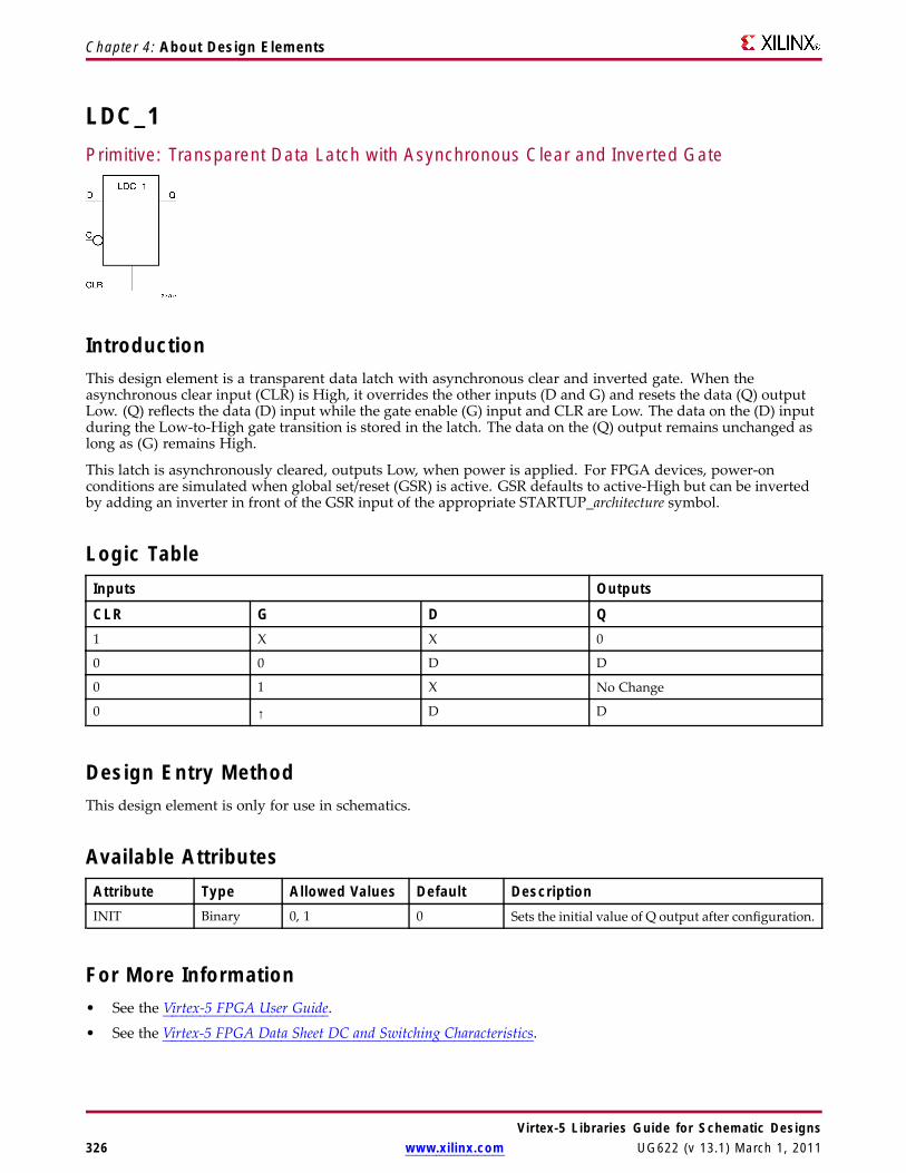
Chapter 4: About Design Elements
LDC_1Primitive: Transparent Data Latch with Asynchronous Clear and Inverted Gate
IntroductionThis design element is a transparent data latch with asynchronous clear and inverted gate. When theasynchronous clear input (CLR) is High, it overrides the other inputs (D and G) and resets the data (Q) outputLow. (Q) reflects the data (D) input while the gate enable (G) input and CLR are Low. The data on the (D) inputduring the Low-to-High gate transition is stored in the latch. The data on the (Q) output remains unchanged aslong as (G) remains High.
This latch is asynchronously cleared, outputs Low, when power is applied. For FPGA devices, power-onconditions are simulated when global set/reset (GSR) is active. GSR defaults to active-High but can be invertedby adding an inverter in front of the GSR input of the appropriate STARTUP_architecture symbol.
Logic TableInputs Outputs
CLR G D Q1 X X 0
0 0 D D
0 1 X No Change
0 ↑ D D
Design Entry MethodThis design element is only for use in schematics.
Available AttributesAttribute Type Allowed Values Default DescriptionINIT Binary 0, 1 0 Sets the initial value of Q output after configuration.
For More Information• See the Virtex-5 FPGA User Guide.
• See the Virtex-5 FPGA Data Sheet DC and Switching Characteristics.
Virtex-5 Libraries Guide for Schematic Designs326 www.xilinx.com UG622 (v 13.1) March 1, 2011

Chapter 4: About Design Elements
LDCEPrimitive: Transparent Data Latch with Asynchronous Clear and Gate Enable
IntroductionThis design element is a transparent data latch with asynchronous clear and gate enable. When the asynchronousclear input (CLR) is High, it overrides the other inputs and resets the data (Q) output Low. Q reflects the data (D)input while the gate (G) input and gate enable (GE) are High and CLR is Low. If (GE) is Low, data on (D) cannotbe latched. The data on the (D) input during the High-to-Low gate transition is stored in the latch. The data onthe (Q) output remains unchanged as long as (G) or (GE) remains low.
This latch is asynchronously cleared, outputs Low, when power is applied. For FPGA devices, power-onconditions are simulated when global set/reset (GSR) is active. GSR defaults to active-High but can be invertedby adding an inverter in front of the GSR input of the appropriate STARTUP_architecture symbol.
Logic TableInputs Outputs
CLR GE G D Q1 X X X 0
0 0 X X No Change
0 1 1 D D
0 1 0 X No Change
0 1 ↓ D D
Design Entry MethodThis design element can be used in schematics.
Available Attributes
Attribute TypeAllowedValues Default Description
INIT Binary 0, 1 0 Sets the initial value of Q output after configuration.
For More Information• See the Virtex-5 FPGA User Guide.• See the Virtex-5 FPGA Data Sheet DC and Switching Characteristics.
Virtex-5 Libraries Guide for Schematic DesignsUG622 (v 13.1) March 1, 2011 www.xilinx.com 327

Chapter 4: About Design Elements
LDCE_1Primitive: Transparent Data Latch with Asynchronous Clear, Gate Enable, and InvertedGate
IntroductionThis design element is a transparent data latch with asynchronous clear, gate enable, and inverted gate. Whenthe asynchronous clear input (CLR) is High, it overrides the other inputs and resets the data (Q) output Low.(Q) reflects the data (D) input while the gate (G) input and (CLR) are Low and gate enable (GE) is High. Thedata on the (D) input during the Low-to-High gate transition is stored in the latch. The data on the (Q) outputremains unchanged as long as (G) remains High or (GE) remains Low
This latch is asynchronously cleared, outputs Low, when power is applied. For FPGA devices, power-onconditions are simulated when global set/reset (GSR) is active. GSR defaults to active-High but can be invertedby adding an inverter in front of the GSR input of the appropriate STARTUP_architecture symbol.
Logic TableInputs Outputs
CLR GE G D Q1 X X X 0
0 0 X X No Change
0 1 0 D D
0 1 1 X No Change
0 1 ↑ D D
Design Entry MethodThis design element is only for use in schematics.
Available AttributesAttribute Type Allowed Values Default DescriptionINIT Binary 0, 1 0 Sets the initial value of Q output after
configuration.
For More Information• See the Virtex-5 FPGA User Guide.• See the Virtex-5 FPGA Data Sheet DC and Switching Characteristics.
Virtex-5 Libraries Guide for Schematic Designs328 www.xilinx.com UG622 (v 13.1) March 1, 2011

Chapter 4: About Design Elements
LDCPPrimitive: Transparent Data Latch with Asynchronous Clear and Preset
IntroductionThe design element is a transparent data latch with data (D), asynchronous clear (CLR) and preset (PRE) inputs.When CLR is High, it overrides the other inputs and resets the data (Q) output Low. When PRE is High and CLRis low, it presets the data (Q) output High. Q reflects the data (D) input while the gate (G) input is High andCLR and PRE are Low. The data on the D input during the High-to-Low gate transition is stored in the latch.The data on the Q output remains unchanged as long as G remains Low.
This latch is asynchronously cleared, outputs Low, when power is applied. For FPGA devices, power-onconditions are simulated when global set/reset (GSR) is active. GSR defaults to active-High but can be invertedby adding an inverter in front of the GSR input of the appropriate STARTUP_architecture symbol.
Logic TableInputs Outputs
CLR PRE G D Q1 X X X 0
0 1 X X 1
0 0 1 D D
0 0 0 X No Change
0 0 ↓ D D
Design Entry MethodThis design element is only for use in schematics.
Available AttributesAttribute Type Allowed Values Default DescriptionINIT Integer 0, 1 0 Specifies the initial value upon power-up or the
assertion of GSR for the (Q) port.
For More Information• See the Virtex-5 FPGA User Guide.• See the Virtex-5 FPGA Data Sheet DC and Switching Characteristics.
Virtex-5 Libraries Guide for Schematic DesignsUG622 (v 13.1) March 1, 2011 www.xilinx.com 329

Chapter 4: About Design Elements
LDCP_1Primitive: Transparent Data Latch with Asynchronous Clear and Preset and Inverted Gate
IntroductionThis design element is a transparent data latch with data (D), asynchronous clear (CLR), preset (PRE) inputs, andinverted gate (G). When (CLR) is High, it overrides the other inputs and resets the data (Q) output Low. When(PRE) is High and (CLR) is Low, it presets the data (Q) output High. (Q) reflects the data (D) input while gate (G)input, (CLR), and (PRE) are Low. The data on the (D) input during the Low-to-High gate transition is stored inthe latch. The data on the (Q) output remains unchanged as long as (G) remains High.
This latch is asynchronously cleared, outputs Low, when power is applied. For FPGA devices, power-onconditions are simulated when global set/reset (GSR) is active. GSR defaults to active-High but can be invertedby adding an inverter in front of the GSR input of the appropriate STARTUP_architecture symbol.
Logic TableInputs Outputs
CLR PRE G D Q1 X X X 0
0 1 X X 1
0 0 0 D D
0 0 1 X No Change
0 0 ↑ D D
Design Entry MethodThis design element is only for use in schematics.
Available AttributesAttribute Type Allowed Values Default DescriptionINIT Integer 0, 1 0 Specifies the initial value upon power-up or the assertion
of GSR for the (Q) port.
For More Information• See the Virtex-5 FPGA User Guide.• See the Virtex-5 FPGA Data Sheet DC and Switching Characteristics.
Virtex-5 Libraries Guide for Schematic Designs330 www.xilinx.com UG622 (v 13.1) March 1, 2011
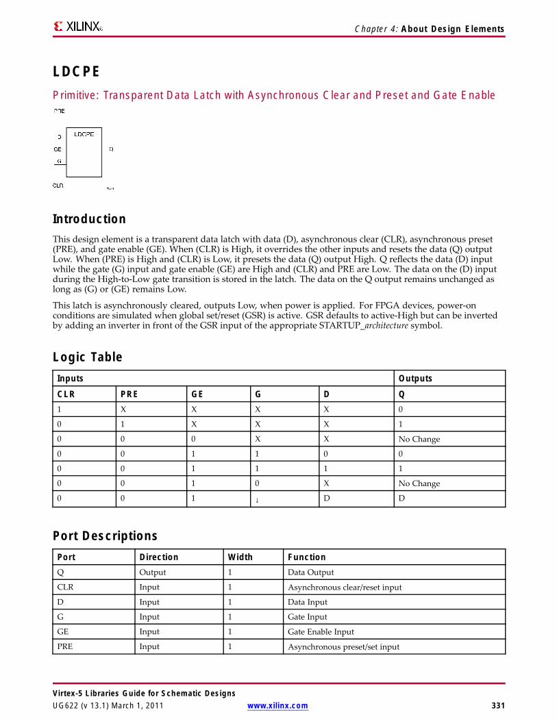
Chapter 4: About Design Elements
LDCPEPrimitive: Transparent Data Latch with Asynchronous Clear and Preset and Gate Enable
IntroductionThis design element is a transparent data latch with data (D), asynchronous clear (CLR), asynchronous preset(PRE), and gate enable (GE). When (CLR) is High, it overrides the other inputs and resets the data (Q) outputLow. When (PRE) is High and (CLR) is Low, it presets the data (Q) output High. Q reflects the data (D) inputwhile the gate (G) input and gate enable (GE) are High and (CLR) and PRE are Low. The data on the (D) inputduring the High-to-Low gate transition is stored in the latch. The data on the Q output remains unchanged aslong as (G) or (GE) remains Low.
This latch is asynchronously cleared, outputs Low, when power is applied. For FPGA devices, power-onconditions are simulated when global set/reset (GSR) is active. GSR defaults to active-High but can be invertedby adding an inverter in front of the GSR input of the appropriate STARTUP_architecture symbol.
Logic TableInputs Outputs
CLR PRE GE G D Q1 X X X X 0
0 1 X X X 1
0 0 0 X X No Change
0 0 1 1 0 0
0 0 1 1 1 1
0 0 1 0 X No Change
0 0 1 ↓ D D
Port DescriptionsPort Direction Width FunctionQ Output 1 Data Output
CLR Input 1 Asynchronous clear/reset input
D Input 1 Data Input
G Input 1 Gate Input
GE Input 1 Gate Enable Input
PRE Input 1 Asynchronous preset/set input
Virtex-5 Libraries Guide for Schematic DesignsUG622 (v 13.1) March 1, 2011 www.xilinx.com 331
Chapter 4: About Design Elements
Design Entry MethodThis design element can be used in schematics.
Available AttributesAttribute Type Allowed Values Default DescriptionINIT Integer 0, 1 0 Sets the initial value of Q output after configuration.
For More Information• See the Virtex-5 FPGA User Guide.
• See the Virtex-5 FPGA Data Sheet DC and Switching Characteristics.
Virtex-5 Libraries Guide for Schematic Designs332 www.xilinx.com UG622 (v 13.1) March 1, 2011
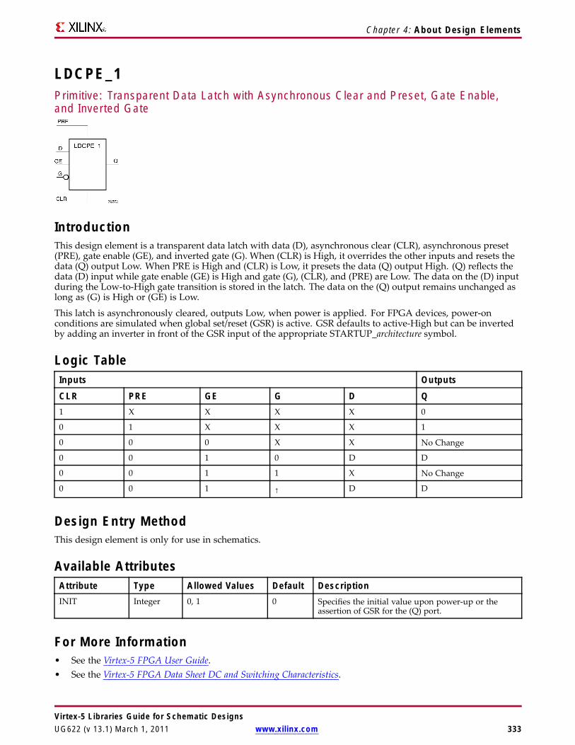
Chapter 4: About Design Elements
LDCPE_1Primitive: Transparent Data Latch with Asynchronous Clear and Preset, Gate Enable,and Inverted Gate
IntroductionThis design element is a transparent data latch with data (D), asynchronous clear (CLR), asynchronous preset(PRE), gate enable (GE), and inverted gate (G). When (CLR) is High, it overrides the other inputs and resets thedata (Q) output Low. When PRE is High and (CLR) is Low, it presets the data (Q) output High. (Q) reflects thedata (D) input while gate enable (GE) is High and gate (G), (CLR), and (PRE) are Low. The data on the (D) inputduring the Low-to-High gate transition is stored in the latch. The data on the (Q) output remains unchanged aslong as (G) is High or (GE) is Low.
This latch is asynchronously cleared, outputs Low, when power is applied. For FPGA devices, power-onconditions are simulated when global set/reset (GSR) is active. GSR defaults to active-High but can be invertedby adding an inverter in front of the GSR input of the appropriate STARTUP_architecture symbol.
Logic TableInputs Outputs
CLR PRE GE G D Q1 X X X X 0
0 1 X X X 1
0 0 0 X X No Change
0 0 1 0 D D
0 0 1 1 X No Change
0 0 1 ↑ D D
Design Entry MethodThis design element is only for use in schematics.
Available AttributesAttribute Type Allowed Values Default DescriptionINIT Integer 0, 1 0 Specifies the initial value upon power-up or the
assertion of GSR for the (Q) port.
For More Information• See the Virtex-5 FPGA User Guide.• See the Virtex-5 FPGA Data Sheet DC and Switching Characteristics.
Virtex-5 Libraries Guide for Schematic DesignsUG622 (v 13.1) March 1, 2011 www.xilinx.com 333

Chapter 4: About Design Elements
LDEPrimitive: Transparent Data Latch with Gate Enable
IntroductionThis design element is a transparent data latch with data (D) and gate enable (GE) inputs. Output (Q) reflectsthe data (D) while the gate (G) input and gate enable (GE) are High. The data on the (D) input during theHigh-to-Low gate transition is stored in the latch. The data on the (Q) output remains unchanged as long as(G) or (GE) remains Low.
This latch is asynchronously cleared, outputs Low, when power is applied. For FPGA devices, power-onconditions are simulated when global set/reset (GSR) is active. GSR defaults to active-High but can be invertedby adding an inverter in front of the GSR input of the appropriate STARTUP_architecture symbol.
Logic TableInputs Outputs
GE G D Q0 X X No Change
1 1 D D
1 0 X No Change
1 ↓ D D
Design Entry MethodThis design element is only for use in schematics.
Available Attributes
Attribute TypeAllowedValues Default Description
INIT Binary 0, 1 0 Specifies the initial value upon power-up or the assertion ofGSR for the (Q) port.
For More Information• See the Virtex-5 FPGA User Guide.
• See the Virtex-5 FPGA Data Sheet DC and Switching Characteristics.
Virtex-5 Libraries Guide for Schematic Designs334 www.xilinx.com UG622 (v 13.1) March 1, 2011
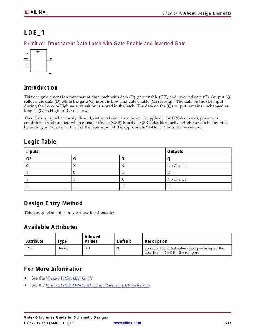
Chapter 4: About Design Elements
LDE_1Primitive: Transparent Data Latch with Gate Enable and Inverted Gate
IntroductionThis design element is a transparent data latch with data (D), gate enable (GE), and inverted gate (G). Output (Q)reflects the data (D) while the gate (G) input is Low and gate enable (GE) is High. The data on the (D) inputduring the Low-to-High gate transition is stored in the latch. The data on the (Q) output remains unchanged aslong as (G) is High or (GE) is Low.
This latch is asynchronously cleared, outputs Low, when power is applied. For FPGA devices, power-onconditions are simulated when global set/reset (GSR) is active. GSR defaults to active-High but can be invertedby adding an inverter in front of the GSR input of the appropriate STARTUP_architecture symbol.
Logic TableInputs Outputs
GE G D Q0 X X No Change
1 0 D D
1 1 X No Change
1 ↑ D D
Design Entry MethodThis design element is only for use in schematics.
Available Attributes
Attribute TypeAllowedValues Default Description
INIT Binary 0, 1 0 Specifies the initial value upon power-up or theassertion of GSR for the (Q) port.
For More Information• See the Virtex-5 FPGA User Guide.
• See the Virtex-5 FPGA Data Sheet DC and Switching Characteristics.
Virtex-5 Libraries Guide for Schematic DesignsUG622 (v 13.1) March 1, 2011 www.xilinx.com 335
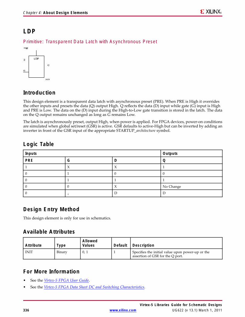
Chapter 4: About Design Elements
LDPPrimitive: Transparent Data Latch with Asynchronous Preset
IntroductionThis design element is a transparent data latch with asynchronous preset (PRE). When PRE is High it overridesthe other inputs and presets the data (Q) output High. Q reflects the data (D) input while gate (G) input is Highand PRE is Low. The data on the (D) input during the High-to-Low gate transition is stored in the latch. The dataon the Q output remains unchanged as long as G remains Low.
The latch is asynchronously preset, output High, when power is applied. For FPGA devices, power-on conditionsare simulated when global set/reset (GSR) is active. GSR defaults to active-High but can be inverted by adding aninverter in front of the GSR input of the appropriate STARTUP_architecture symbol.
Logic TableInputs Outputs
PRE G D Q1 X X 1
0 1 0 0
0 1 1 1
0 0 X No Change
0 ↓ D D
Design Entry MethodThis design element is only for use in schematics.
Available Attributes
Attribute TypeAllowedValues Default Description
INIT Binary 0, 1 1 Specifies the initial value upon power-up or theassertion of GSR for the Q port.
For More Information• See the Virtex-5 FPGA User Guide.
• See the Virtex-5 FPGA Data Sheet DC and Switching Characteristics.
Virtex-5 Libraries Guide for Schematic Designs336 www.xilinx.com UG622 (v 13.1) March 1, 2011
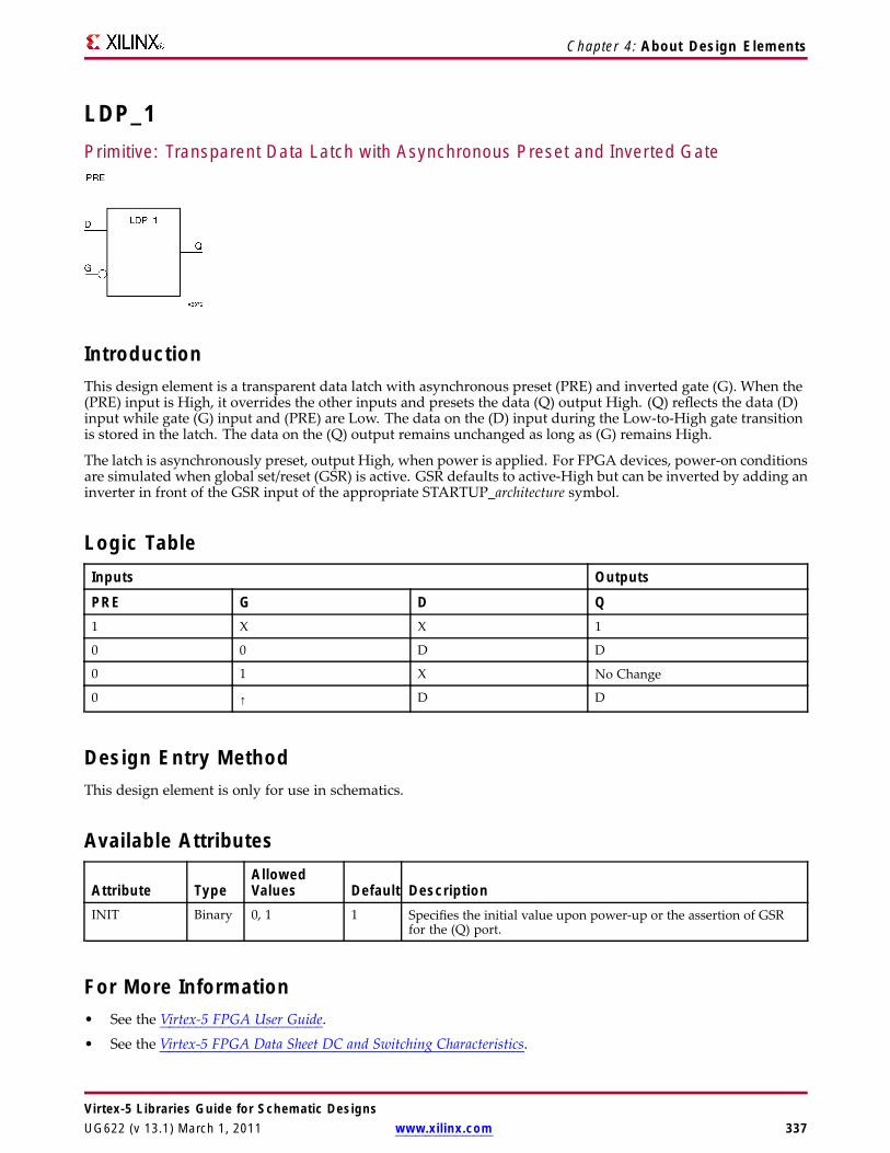
Chapter 4: About Design Elements
LDP_1Primitive: Transparent Data Latch with Asynchronous Preset and Inverted Gate
IntroductionThis design element is a transparent data latch with asynchronous preset (PRE) and inverted gate (G). When the(PRE) input is High, it overrides the other inputs and presets the data (Q) output High. (Q) reflects the data (D)input while gate (G) input and (PRE) are Low. The data on the (D) input during the Low-to-High gate transitionis stored in the latch. The data on the (Q) output remains unchanged as long as (G) remains High.
The latch is asynchronously preset, output High, when power is applied. For FPGA devices, power-on conditionsare simulated when global set/reset (GSR) is active. GSR defaults to active-High but can be inverted by adding aninverter in front of the GSR input of the appropriate STARTUP_architecture symbol.
Logic TableInputs Outputs
PRE G D Q1 X X 1
0 0 D D
0 1 X No Change
0 ↑ D D
Design Entry MethodThis design element is only for use in schematics.
Available Attributes
Attribute TypeAllowedValues Default Description
INIT Binary 0, 1 1 Specifies the initial value upon power-up or the assertion of GSRfor the (Q) port.
For More Information• See the Virtex-5 FPGA User Guide.
• See the Virtex-5 FPGA Data Sheet DC and Switching Characteristics.
Virtex-5 Libraries Guide for Schematic DesignsUG622 (v 13.1) March 1, 2011 www.xilinx.com 337
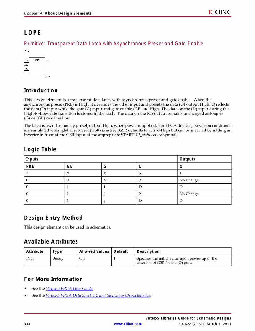
Chapter 4: About Design Elements
LDPEPrimitive: Transparent Data Latch with Asynchronous Preset and Gate Enable
IntroductionThis design element is a transparent data latch with asynchronous preset and gate enable. When theasynchronous preset (PRE) is High, it overrides the other input and presets the data (Q) output High. Q reflectsthe data (D) input while the gate (G) input and gate enable (GE) are High. The data on the (D) input during theHigh-to-Low gate transition is stored in the latch. The data on the (Q) output remains unchanged as long as(G) or (GE) remains Low.
The latch is asynchronously preset, output High, when power is applied. For FPGA devices, power-on conditionsare simulated when global set/reset (GSR) is active. GSR defaults to active-High but can be inverted by adding aninverter in front of the GSR input of the appropriate STARTUP_architecture symbol.
Logic TableInputs Outputs
PRE GE G D Q1 X X X 1
0 0 X X No Change
0 1 1 D D
0 1 0 X No Change
0 1 ↓ D D
Design Entry MethodThis design element can be used in schematics.
Available AttributesAttribute Type Allowed Values Default DescriptionINIT Binary 0, 1 1 Specifies the initial value upon power-up or the
assertion of GSR for the (Q) port.
For More Information• See the Virtex-5 FPGA User Guide.
• See the Virtex-5 FPGA Data Sheet DC and Switching Characteristics.
Virtex-5 Libraries Guide for Schematic Designs338 www.xilinx.com UG622 (v 13.1) March 1, 2011

Chapter 4: About Design Elements
LDPE_1Primitive: Transparent Data Latch with Asynchronous Preset, Gate Enable, and InvertedGate
IntroductionThis design element is a transparent data latch with asynchronous preset, gate enable, and inverted gate. Whenthe asynchronous preset (PRE) is High, it overrides the other input and presets the data (Q) output High. (Q)reflects the data (D) input while the gate (G) and (PRE) are Low and gate enable (GE) is High. The data on the(D) input during the Low-to-High gate transition is stored in the latch. The data on the (Q) output remainsunchanged as long as (G) remains High or (GE) remains Low.
The latch is asynchronously preset, output High, when power is applied. For FPGA devices, power-on conditionsare simulated when global set/reset (GSR) is active. GSR defaults to active-High but can be inverted by adding aninverter in front of the GSR input of the appropriate STARTUP_architecture symbol.
Logic TableInputs Outputs
PRE GE G D Q1 X X X 1
0 0 X X No Change
0 1 0 D D
0 1 1 X No Change
0 1 ↑ D D
Design Entry MethodThis design element is only for use in schematics.
Available AttributesAttribute Type Allowed Values Default DescriptionINIT Binary 0, 1 1 Specifies the initial value upon power-up or the assertion
of GSR for the (Q) port.
For More Information• See the Virtex-5 FPGA User Guide.• See the Virtex-5 FPGA Data Sheet DC and Switching Characteristics.
Virtex-5 Libraries Guide for Schematic DesignsUG622 (v 13.1) March 1, 2011 www.xilinx.com 339
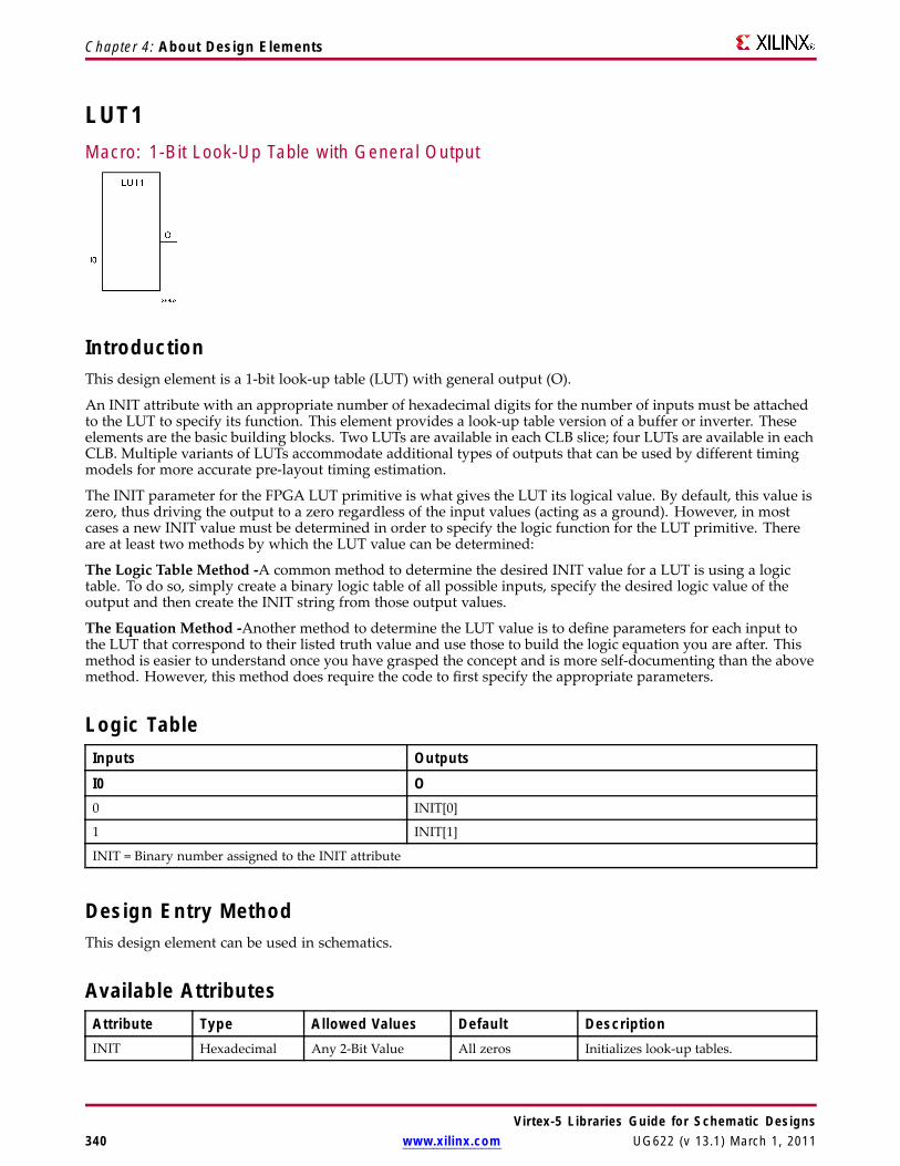
Chapter 4: About Design Elements
LUT1Macro: 1-Bit Look-Up Table with General Output
IntroductionThis design element is a 1-bit look-up table (LUT) with general output (O).
An INIT attribute with an appropriate number of hexadecimal digits for the number of inputs must be attachedto the LUT to specify its function. This element provides a look-up table version of a buffer or inverter. Theseelements are the basic building blocks. Two LUTs are available in each CLB slice; four LUTs are available in eachCLB. Multiple variants of LUTs accommodate additional types of outputs that can be used by different timingmodels for more accurate pre-layout timing estimation.
The INIT parameter for the FPGA LUT primitive is what gives the LUT its logical value. By default, this value iszero, thus driving the output to a zero regardless of the input values (acting as a ground). However, in mostcases a new INIT value must be determined in order to specify the logic function for the LUT primitive. Thereare at least two methods by which the LUT value can be determined:
The Logic Table Method -A common method to determine the desired INIT value for a LUT is using a logictable. To do so, simply create a binary logic table of all possible inputs, specify the desired logic value of theoutput and then create the INIT string from those output values.
The Equation Method -Another method to determine the LUT value is to define parameters for each input tothe LUT that correspond to their listed truth value and use those to build the logic equation you are after. Thismethod is easier to understand once you have grasped the concept and is more self-documenting than the abovemethod. However, this method does require the code to first specify the appropriate parameters.
Logic TableInputs Outputs
I0 O0 INIT[0]
1 INIT[1]
INIT = Binary number assigned to the INIT attribute
Design Entry MethodThis design element can be used in schematics.
Available AttributesAttribute Type Allowed Values Default DescriptionINIT Hexadecimal Any 2-Bit Value All zeros Initializes look-up tables.
Virtex-5 Libraries Guide for Schematic Designs340 www.xilinx.com UG622 (v 13.1) March 1, 2011

Chapter 4: About Design Elements
For More Information• See the Virtex-5 FPGA User Guide.
• See the Virtex-5 FPGA Data Sheet DC and Switching Characteristics.
Virtex-5 Libraries Guide for Schematic DesignsUG622 (v 13.1) March 1, 2011 www.xilinx.com 341

Chapter 4: About Design Elements
LUT1_DMacro: 1-Bit Look-Up Table with Dual Output
IntroductionThis design element is a 1-bit look-up table (LUT) with two functionally identical outputs, O and LO. It providesa look-up table version of a buffer or inverter.
The O output is a general interconnect. The LO output is used to connect to another output within the same CLBslice and to the fast connect buffer. A mandatory INIT attribute, with an appropriate number of hexadecimaldigits for the number of inputs, must be attached to the LUT to specify its function.
The INIT parameter for the FPGA LUT primitive is what gives the LUT its logical value. By default, this value iszero, thus driving the output to a zero regardless of the input values (acting as a ground). However, in mostcases a new INIT value must be determined in order to specify the logic function for the LUT primitive. Thereare at least two methods by which the LUT value can be determined:
The Logic Table Method -A common method to determine the desired INIT value for a LUT is using a logictable. To do so, simply create a binary logic table of all possible inputs, specify the desired logic value of theoutput and then create the INIT string from those output values.
The Equation Method -Another method to determine the LUT value is to define parameters for each input tothe LUT that correspond to their listed truth value and use those to build the logic equation you are after. Thismethod is easier to understand once you have grasped the concept and is more self-documenting than the abovemethod. However, this method does require the code to first specify the appropriate parameters.
Logic TableInputs Outputs
I0 O LO0 INIT[0] INIT[0]
1 INIT[1] INIT[1]
INIT = Binary number assigned to the INIT attribute
Design Entry MethodThis design element can be used in schematics.
Available AttributesAttribute Type Allowed Values Default DescriptionINIT Hexadecimal Any 2-Bit Value All zeros Initializes look-up tables.
For More Information• See the Virtex-5 FPGA User Guide.• See the Virtex-5 FPGA Data Sheet DC and Switching Characteristics.
Virtex-5 Libraries Guide for Schematic Designs342 www.xilinx.com UG622 (v 13.1) March 1, 2011

Chapter 4: About Design Elements
LUT1_LMacro: 1-Bit Look-Up Table with Local Output
IntroductionThis design element is a 1-bit look-up table (LUT) with a local output (LO) that is used to connect to anotheroutput within the same CLB slice and to the fast connect buffer. It provides a look-up table version of a bufferor inverter.
A mandatory INIT attribute, with an appropriate number of hexadecimal digits for the number of inputs,must be attached to the LUT to specify its function.
The INIT parameter for the FPGA LUT primitive is what gives the LUT its logical value. By default, this value iszero, thus driving the output to a zero regardless of the input values (acting as a ground). However, in mostcases a new INIT value must be determined in order to specify the logic function for the LUT primitive. Thereare at least two methods by which the LUT value can be determined:
The Logic Table Method -A common method to determine the desired INIT value for a LUT is using a logictable. To do so, simply create a binary logic table of all possible inputs, specify the desired logic value of theoutput and then create the INIT string from those output values.
The Equation Method -Another method to determine the LUT value is to define parameters for each input tothe LUT that correspond to their listed truth value and use those to build the logic equation you are after. Thismethod is easier to understand once you have grasped the concept and is more self-documenting than the abovemethod. However, this method does require the code to first specify the appropriate parameters.
Logic TableInputs Outputs
I0 LO0 INIT[0]
1 INIT[1]
INIT = Binary number assigned to the INIT attribute
Design Entry MethodThis design element can be used in schematics.
Available AttributesAttribute Type Allowed Values Default DescriptionINIT Hexadecimal Any 2-Bit Value All zeros Initializes look-up tables.
For More Information• See the Virtex-5 FPGA User Guide.• See the Virtex-5 FPGA Data Sheet DC and Switching Characteristics.
Virtex-5 Libraries Guide for Schematic DesignsUG622 (v 13.1) March 1, 2011 www.xilinx.com 343
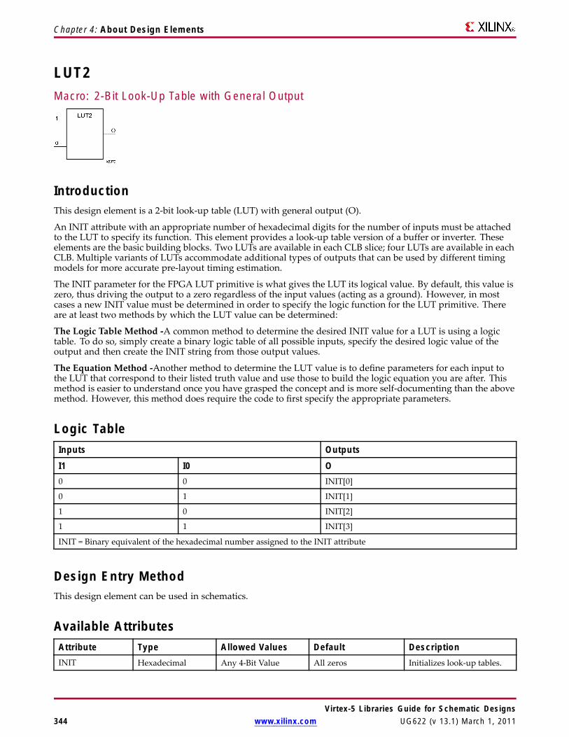
Chapter 4: About Design Elements
LUT2Macro: 2-Bit Look-Up Table with General Output
IntroductionThis design element is a 2-bit look-up table (LUT) with general output (O).
An INIT attribute with an appropriate number of hexadecimal digits for the number of inputs must be attachedto the LUT to specify its function. This element provides a look-up table version of a buffer or inverter. Theseelements are the basic building blocks. Two LUTs are available in each CLB slice; four LUTs are available in eachCLB. Multiple variants of LUTs accommodate additional types of outputs that can be used by different timingmodels for more accurate pre-layout timing estimation.
The INIT parameter for the FPGA LUT primitive is what gives the LUT its logical value. By default, this value iszero, thus driving the output to a zero regardless of the input values (acting as a ground). However, in mostcases a new INIT value must be determined in order to specify the logic function for the LUT primitive. Thereare at least two methods by which the LUT value can be determined:
The Logic Table Method -A common method to determine the desired INIT value for a LUT is using a logictable. To do so, simply create a binary logic table of all possible inputs, specify the desired logic value of theoutput and then create the INIT string from those output values.
The Equation Method -Another method to determine the LUT value is to define parameters for each input tothe LUT that correspond to their listed truth value and use those to build the logic equation you are after. Thismethod is easier to understand once you have grasped the concept and is more self-documenting than the abovemethod. However, this method does require the code to first specify the appropriate parameters.
Logic TableInputs Outputs
I1 I0 O0 0 INIT[0]
0 1 INIT[1]
1 0 INIT[2]
1 1 INIT[3]
INIT = Binary equivalent of the hexadecimal number assigned to the INIT attribute
Design Entry MethodThis design element can be used in schematics.
Available AttributesAttribute Type Allowed Values Default DescriptionINIT Hexadecimal Any 4-Bit Value All zeros Initializes look-up tables.
Virtex-5 Libraries Guide for Schematic Designs344 www.xilinx.com UG622 (v 13.1) March 1, 2011

Chapter 4: About Design Elements
For More Information• See the Virtex-5 FPGA User Guide.
• See the Virtex-5 FPGA Data Sheet DC and Switching Characteristics.
Virtex-5 Libraries Guide for Schematic DesignsUG622 (v 13.1) March 1, 2011 www.xilinx.com 345

Chapter 4: About Design Elements
LUT2_DMacro: 2-Bit Look-Up Table with Dual Output
IntroductionThis design element is a 2-bit look-up table (LUT) with two functionally identical outputs, O and LO.
The O output is a general interconnect. The LO output is used to connect to another output within the same CLBslice and to the fast connect buffer. A mandatory INIT attribute, with an appropriate number of hexadecimaldigits for the number of inputs, must be attached to the LUT to specify its function.
The INIT parameter for the FPGA LUT primitive is what gives the LUT its logical value. By default, this value iszero, thus driving the output to a zero regardless of the input values (acting as a ground). However, in mostcases a new INIT value must be determined in order to specify the logic function for the LUT primitive. Thereare at least two methods by which the LUT value can be determined:
The LogicTable Method -A common method to determine the desired INIT value for a LUT is using a logictable. To do so, simply create a binary logic table of all possible inputs, specify the desired logic value of theoutput and then create the INIT string from those output values.
The Equation Method -Another method to determine the LUT value is to define parameters for each input tothe LUT that correspond to their listed truth value and use those to build the logic equation you are after. Thismethod is easier to understand once you have grasped the concept and is more self-documenting than the abovemethod. However, this method does require the code to first specify the appropriate parameters.
Logic TableInputs Outputs
I1 I0 O LO0 0 INIT[0] INIT[0]
0 1 INIT[1] INIT[1]
1 0 INIT[2] INIT[2]
1 1 INIT[3] INIT[3]
INIT = Binary equivalent of the hexadecimal number assigned to the INIT attribute
Design Entry MethodThis design element can be used in schematics.
Available AttributesAttribute Type Allowed Values Default DescriptionINIT Hexadecimal Any 4-Bit Value All zeros Initializes look-up tables.
Virtex-5 Libraries Guide for Schematic Designs346 www.xilinx.com UG622 (v 13.1) March 1, 2011

Chapter 4: About Design Elements
For More Information• See the Virtex-5 FPGA User Guide.
• See the Virtex-5 FPGA Data Sheet DC and Switching Characteristics.
Virtex-5 Libraries Guide for Schematic DesignsUG622 (v 13.1) March 1, 2011 www.xilinx.com 347

Chapter 4: About Design Elements
LUT2_LMacro: 2-Bit Look-Up Table with Local Output
IntroductionThis design element is a 2-bit look-up table (LUT) with a local output (LO) that is used to connect to anotheroutput within the same CLB slice and to the fast connect buffer. It provides a look-up table version of a bufferor inverter.
A mandatory INIT attribute, with an appropriate number of hexadecimal digits for the number of inputs,must be attached to the LUT to specify its function.
The INIT parameter for the FPGA LUT primitive is what gives the LUT its logical value. By default, this value iszero, thus driving the output to a zero regardless of the input values (acting as a ground). However, in mostcases a new INIT value must be determined in order to specify the logic function for the LUT primitive. Thereare at least two methods by which the LUT value can be determined:
The Logic Table Method -A common method to determine the desired INIT value for a LUT is using a logictable. To do so, simply create a binary logic table of all possible inputs, specify the desired logic value of theoutput and then create the INIT string from those output values.
The Equation Method -Another method to determine the LUT value is to define parameters for each input tothe LUT that correspond to their listed truth value and use those to build the logic equation you are after. Thismethod is easier to understand once you have grasped the concept and is more self-documenting than the abovemethod. However, this method does require the code to first specify the appropriate parameters.
Logic TableInputs Outputs
I1 I0 LO0 0 INIT[0]
0 1 INIT[1]
1 0 INIT[2]
1 1 INIT[3]
INIT = Binary equivalent of the hexadecimal number assigned to the INIT attribute
Design Entry MethodThis design element can be used in schematics.
Available AttributesAttribute Type Allowed Values Default DescriptionINIT Hexadecimal Any 4-Bit Value All zeros Initializes look-up tables.
Virtex-5 Libraries Guide for Schematic Designs348 www.xilinx.com UG622 (v 13.1) March 1, 2011

Chapter 4: About Design Elements
For More Information• See the Virtex-5 FPGA User Guide.
• See the Virtex-5 FPGA Data Sheet DC and Switching Characteristics.
Virtex-5 Libraries Guide for Schematic DesignsUG622 (v 13.1) March 1, 2011 www.xilinx.com 349
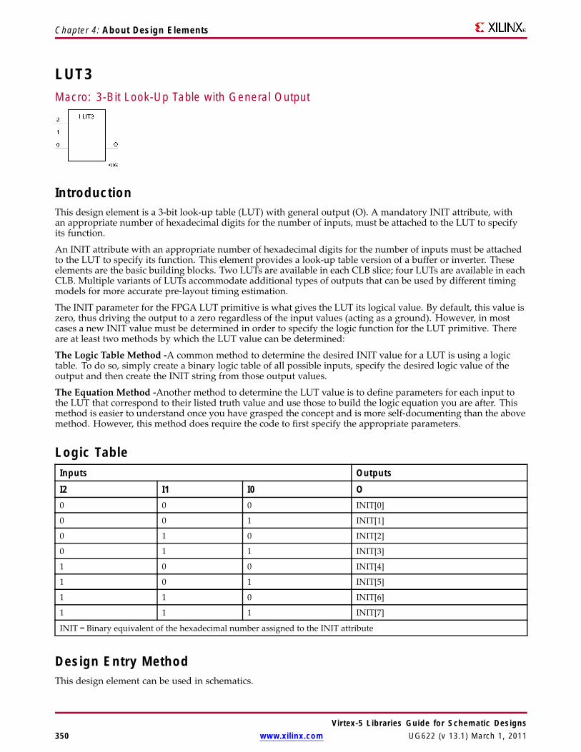
Chapter 4: About Design Elements
LUT3Macro: 3-Bit Look-Up Table with General Output
IntroductionThis design element is a 3-bit look-up table (LUT) with general output (O). A mandatory INIT attribute, withan appropriate number of hexadecimal digits for the number of inputs, must be attached to the LUT to specifyits function.
An INIT attribute with an appropriate number of hexadecimal digits for the number of inputs must be attachedto the LUT to specify its function. This element provides a look-up table version of a buffer or inverter. Theseelements are the basic building blocks. Two LUTs are available in each CLB slice; four LUTs are available in eachCLB. Multiple variants of LUTs accommodate additional types of outputs that can be used by different timingmodels for more accurate pre-layout timing estimation.
The INIT parameter for the FPGA LUT primitive is what gives the LUT its logical value. By default, this value iszero, thus driving the output to a zero regardless of the input values (acting as a ground). However, in mostcases a new INIT value must be determined in order to specify the logic function for the LUT primitive. Thereare at least two methods by which the LUT value can be determined:
The Logic Table Method -A common method to determine the desired INIT value for a LUT is using a logictable. To do so, simply create a binary logic table of all possible inputs, specify the desired logic value of theoutput and then create the INIT string from those output values.
The Equation Method -Another method to determine the LUT value is to define parameters for each input tothe LUT that correspond to their listed truth value and use those to build the logic equation you are after. Thismethod is easier to understand once you have grasped the concept and is more self-documenting than the abovemethod. However, this method does require the code to first specify the appropriate parameters.
Logic TableInputs Outputs
I2 I1 I0 O0 0 0 INIT[0]
0 0 1 INIT[1]
0 1 0 INIT[2]
0 1 1 INIT[3]
1 0 0 INIT[4]
1 0 1 INIT[5]
1 1 0 INIT[6]
1 1 1 INIT[7]
INIT = Binary equivalent of the hexadecimal number assigned to the INIT attribute
Design Entry MethodThis design element can be used in schematics.
Virtex-5 Libraries Guide for Schematic Designs350 www.xilinx.com UG622 (v 13.1) March 1, 2011

Chapter 4: About Design Elements
Available AttributesAttribute Type Allowed Values Default DescriptionINIT Hexadecimal Any 8-Bit Value All zeros Initializes look-up tables.
For More Information• See the Virtex-5 FPGA User Guide.
• See the Virtex-5 FPGA Data Sheet DC and Switching Characteristics.
Virtex-5 Libraries Guide for Schematic DesignsUG622 (v 13.1) March 1, 2011 www.xilinx.com 351

Chapter 4: About Design Elements
LUT3_DMacro: 3-Bit Look-Up Table with Dual Output
IntroductionThis design element is a 3-bit look-up table (LUT) with two functionally identical outputs, O and LO.
The O output is a general interconnect. The LO output is used to connect to another output within the same CLBslice and to the fast connect buffer. A mandatory INIT attribute, with an appropriate number of hexadecimaldigits for the number of inputs, must be attached to the LUT to specify its function.
The INIT parameter for the FPGA LUT primitive is what gives the LUT its logical value. By default, this value iszero, thus driving the output to a zero regardless of the input values (acting as a ground). However, in mostcases a new INIT value must be determined in order to specify the logic function for the LUT primitive. Thereare at least two methods by which the LUT value can be determined:
The Logic Table Method -A common method to determine the desired INIT value for a LUT is using a logictable. To do so, simply create a binary logic table of all possible inputs, specify the desired logic value of theoutput and then create the INIT string from those output values.
The Equation Method -Another method to determine the LUT value is to define parameters for each input tothe LUT that correspond to their listed truth value and use those to build the logic equation you are after. Thismethod is easier to understand once you have grasped the concept and is more self-documenting than the abovemethod. However, this method does require the code to first specify the appropriate parameters.
Logic TableInputs Outputs
I2 I1 I0 O LO0 0 0 INIT[0] INIT[0]
0 0 1 INIT[1] INIT[1]
0 1 0 INIT[2] INIT[2]
0 1 1 INIT[3] INIT[3]
1 0 0 INIT[4] INIT[4]
1 0 1 INIT[5] INIT[5]
1 1 0 INIT[6] INIT[6]
1 1 1 INIT[7] INIT[7]
INIT = Binary equivalent of the hexadecimal number assigned to the INIT attribute
Design Entry MethodThis design element can be used in schematics.
Virtex-5 Libraries Guide for Schematic Designs352 www.xilinx.com UG622 (v 13.1) March 1, 2011

Chapter 4: About Design Elements
Available AttributesAttribute Type Allowed Values Default DescriptionINIT Hexadecimal Any 8-Bit Value All zeros Initializes look-up tables.
For More Information• See the Virtex-5 FPGA User Guide.
• See the Virtex-5 FPGA Data Sheet DC and Switching Characteristics.
Virtex-5 Libraries Guide for Schematic DesignsUG622 (v 13.1) March 1, 2011 www.xilinx.com 353
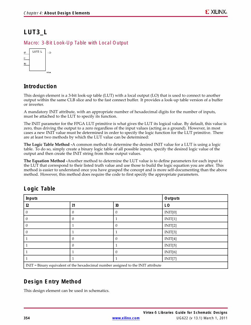
Chapter 4: About Design Elements
LUT3_LMacro: 3-Bit Look-Up Table with Local Output
IntroductionThis design element is a 3-bit look-up table (LUT) with a local output (LO) that is used to connect to anotheroutput within the same CLB slice and to the fast connect buffer. It provides a look-up table version of a bufferor inverter.
A mandatory INIT attribute, with an appropriate number of hexadecimal digits for the number of inputs,must be attached to the LUT to specify its function.
The INIT parameter for the FPGA LUT primitive is what gives the LUT its logical value. By default, this value iszero, thus driving the output to a zero regardless of the input values (acting as a ground). However, in mostcases a new INIT value must be determined in order to specify the logic function for the LUT primitive. Thereare at least two methods by which the LUT value can be determined:
The Logic Table Method -A common method to determine the desired INIT value for a LUT is using a logictable. To do so, simply create a binary logic table of all possible inputs, specify the desired logic value of theoutput and then create the INIT string from those output values.
The Equation Method -Another method to determine the LUT value is to define parameters for each input tothe LUT that correspond to their listed truth value and use those to build the logic equation you are after. Thismethod is easier to understand once you have grasped the concept and is more self-documenting than the abovemethod. However, this method does require the code to first specify the appropriate parameters.
Logic TableInputs Outputs
I2 I1 I0 LO0 0 0 INIT[0]
0 0 1 INIT[1]
0 1 0 INIT[2]
0 1 1 INIT[3]
1 0 0 INIT[4]
1 0 1 INIT[5]
1 1 0 INIT[6]
1 1 1 INIT[7]
INIT = Binary equivalent of the hexadecimal number assigned to the INIT attribute
Design Entry MethodThis design element can be used in schematics.
Virtex-5 Libraries Guide for Schematic Designs354 www.xilinx.com UG622 (v 13.1) March 1, 2011

Chapter 4: About Design Elements
Available AttributesAttribute Type Allowed Values Default DescriptionINIT Hexadecimal Any 8-Bit Value All zeros Initializes look-up tables.
For More Information• See the Virtex-5 FPGA User Guide.
• See the Virtex-5 FPGA Data Sheet DC and Switching Characteristics.
Virtex-5 Libraries Guide for Schematic DesignsUG622 (v 13.1) March 1, 2011 www.xilinx.com 355

Chapter 4: About Design Elements
LUT4Macro: 4-Bit Look-Up-Table with General Output
IntroductionThis design element is a 4-bit look-up table (LUT) with general output (O).
An INIT attribute with an appropriate number of hexadecimal digits for the number of inputs must be attachedto the LUT to specify its function. This element provides a look-up table version of a buffer or inverter. Theseelements are the basic building blocks. Two LUTs are available in each CLB slice; four LUTs are available in eachCLB. Multiple variants of LUTs accommodate additional types of outputs that can be used by different timingmodels for more accurate pre-layout timing estimation.
The INIT parameter for the FPGA LUT primitive is what gives the LUT its logical value. By default, this value iszero, thus driving the output to a zero regardless of the input values (acting as a ground). However, in mostcases a new INIT value must be determined in order to specify the logic function for the LUT primitive. Thereare at least two methods by which the LUT value can be determined:
The Logic Table Method -A common method to determine the desired INIT value for a LUT is using a logictable. To do so, simply create a binary logic table of all possible inputs, specify the desired logic value of theoutput and then create the INIT string from those output values.
The Equation Method -Another method to determine the LUT value is to define parameters for each input tothe LUT that correspond to their listed truth value and use those to build the logic equation you are after. Thismethod is easier to understand once you have grasped the concept and is more self-documenting than the abovemethod. However, this method does require the code to first specify the appropriate parameters.
Virtex-5 Libraries Guide for Schematic Designs356 www.xilinx.com UG622 (v 13.1) March 1, 2011
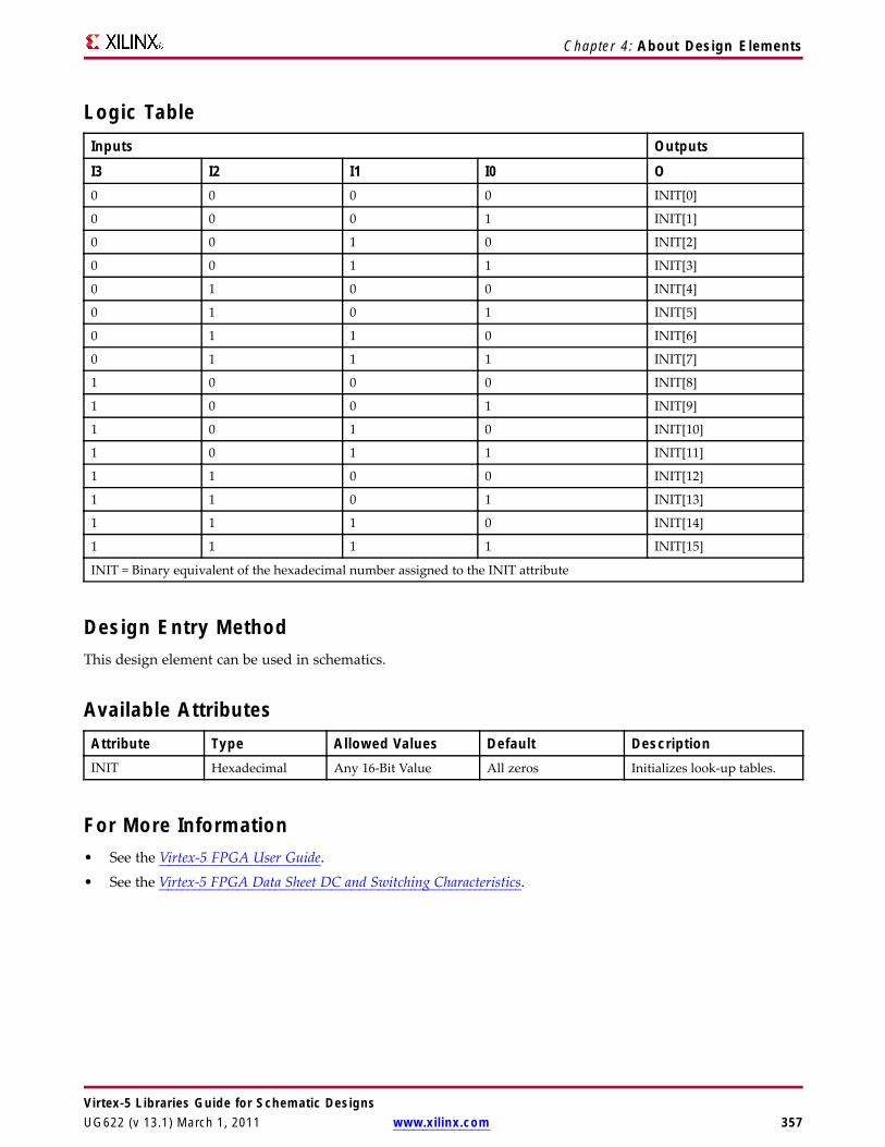
Chapter 4: About Design Elements
Logic TableInputs Outputs
I3 I2 I1 I0 O0 0 0 0 INIT[0]
0 0 0 1 INIT[1]
0 0 1 0 INIT[2]
0 0 1 1 INIT[3]
0 1 0 0 INIT[4]
0 1 0 1 INIT[5]
0 1 1 0 INIT[6]
0 1 1 1 INIT[7]
1 0 0 0 INIT[8]
1 0 0 1 INIT[9]
1 0 1 0 INIT[10]
1 0 1 1 INIT[11]
1 1 0 0 INIT[12]
1 1 0 1 INIT[13]
1 1 1 0 INIT[14]
1 1 1 1 INIT[15]
INIT = Binary equivalent of the hexadecimal number assigned to the INIT attribute
Design Entry MethodThis design element can be used in schematics.
Available AttributesAttribute Type Allowed Values Default DescriptionINIT Hexadecimal Any 16-Bit Value All zeros Initializes look-up tables.
For More Information• See the Virtex-5 FPGA User Guide.
• See the Virtex-5 FPGA Data Sheet DC and Switching Characteristics.
Virtex-5 Libraries Guide for Schematic DesignsUG622 (v 13.1) March 1, 2011 www.xilinx.com 357

Chapter 4: About Design Elements
LUT4_DMacro: 4-Bit Look-Up Table with Dual Output
IntroductionThis design element is a 4-bit look-up table (LUT) with two functionally identical outputs, O and LO
The O output is a general interconnect. The LO output is used to connect to another output within the same CLBslice and to the fast connect buffer. A mandatory INIT attribute, with an appropriate number of hexadecimaldigits for the number of inputs, must be attached to the LUT to specify its function.
The INIT parameter for the FPGA LUT primitive is what gives the LUT its logical value. By default, this value iszero, thus driving the output to a zero regardless of the input values (acting as a ground). However, in mostcases a new INIT value must be determined in order to specify the logic function for the LUT primitive. Thereare at least two methods by which the LUT value can be determined:
The Logic Table Method -A common method to determine the desired INIT value for a LUT is using a logictable. To do so, simply create a binary logic table of all possible inputs, specify the desired logic value of theoutput and then create the INIT string from those output values.
The Equation Method -Another method to determine the LUT value is to define parameters for each input tothe LUT that correspond to their listed truth value and use those to build the logic equation you are after. Thismethod is easier to understand once you have grasped the concept and is more self-documenting than the abovemethod. However, this method does require the code to first specify the appropriate parameters.
Virtex-5 Libraries Guide for Schematic Designs358 www.xilinx.com UG622 (v 13.1) March 1, 2011

Chapter 4: About Design Elements
Logic TableInputs Outputs
I3 I2 I1 I0 O LO0 0 0 0 INIT[0] INIT[0]
0 0 0 1 INIT[1] INIT[1]
0 0 1 0 INIT[2] INIT[2]
0 0 1 1 INIT[3] INIT[3]
0 1 0 0 INIT[4] INIT[4]
0 1 0 1 INIT[5] INIT[5]
0 1 1 0 INIT[6] INIT[6]
0 1 1 1 INIT[7] INIT[7]
1 0 0 0 INIT[8] INIT[8]
1 0 0 1 INIT[9] INIT[9]
1 0 1 0 INIT[10] INIT[10]
1 0 1 1 INIT[11] INIT[11]
1 1 0 0 INIT[12] INIT[12]
1 1 0 1 INIT[13] INIT[13]
1 1 1 0 INIT[14] INIT[14]
1 1 1 1 INIT[15] INIT[15]
INIT = Binary equivalent of the hexadecimal number assigned to the INIT attribute
Design Entry MethodThis design element can be used in schematics.
Available AttributesAttribute Type Allowed Values Default DescriptionINIT Hexadecimal Any 16-Bit Value All zeros Initializes look-up tables.
For More Information• See the Virtex-5 FPGA User Guide.
• See the Virtex-5 FPGA Data Sheet DC and Switching Characteristics.
Virtex-5 Libraries Guide for Schematic DesignsUG622 (v 13.1) March 1, 2011 www.xilinx.com 359

Chapter 4: About Design Elements
LUT4_LMacro: 4-Bit Look-Up Table with Local Output
IntroductionThis design element is a 4-bit look-up table (LUT) with a local output (LO) that is used to connect to anotheroutput within the same CLB slice and to the fast connect buffer. It provides a look-up table version of a bufferor inverter.
A mandatory INIT attribute, with an appropriate number of hexadecimal digits for the number of inputs,must be attached to the LUT to specify its function.
The INIT parameter for the FPGA LUT primitive is what gives the LUT its logical value. By default, this value iszero, thus driving the output to a zero regardless of the input values (acting as a ground). However, in mostcases a new INIT value must be determined in order to specify the logic function for the LUT primitive. Thereare at least two methods by which the LUT value can be determined:
The Logic Table Method -A common method to determine the desired INIT value for a LUT is using a logictable. To do so, simply create a binary logic table of all possible inputs, specify the desired logic value of theoutput and then create the INIT string from those output values.
The Equation Method -Another method to determine the LUT value is to define parameters for each input tothe LUT that correspond to their listed truth value and use those to build the logic equation you are after. Thismethod is easier to understand once you have grasped the concept and more self-documenting than the abovemethod. However, this method does require the code to first specify the appropriate parameters.
Virtex-5 Libraries Guide for Schematic Designs360 www.xilinx.com UG622 (v 13.1) March 1, 2011

Chapter 4: About Design Elements
Logic TableInputs Outputs
I3 I2 I1 I0 LO0 0 0 0 INIT[0]
0 0 0 1 INIT[1]
0 0 1 0 INIT[2]
0 0 1 1 INIT[3]
0 1 0 0 INIT[4]
0 1 0 1 INIT[5]
0 1 1 0 INIT[6]
0 1 1 1 INIT[7]
1 0 0 0 INIT[8]
1 0 0 1 INIT[9]
1 0 1 0 INIT[10]
1 0 1 1 INIT[11]
1 1 0 0 INIT[12]
1 1 0 1 INIT[13]
1 1 1 0 INIT[14]
1 1 1 1 INIT[15]
INIT = Binary equivalent of the hexadecimal number assigned to the INIT attribute
Design Entry MethodThis design element can be used in schematics.
Available AttributesAttribute Type Allowed Values Default DescriptionINIT Hexadecimal Any 16-Bit Value All zeros Initializes look-up tables.
For More Information• See the Virtex-5 FPGA User Guide.
• See the Virtex-5 FPGA Data Sheet DC and Switching Characteristics.
Virtex-5 Libraries Guide for Schematic DesignsUG622 (v 13.1) March 1, 2011 www.xilinx.com 361

Chapter 4: About Design Elements
LUT5Primitive: 5-Input Lookup Table with General Output
IntroductionThis design element is a 5-input, 1-output look-up table (LUT) that can either act as an asynchronous 32-bit ROM(with 5-bit addressing) or implement any 5-input logic function. LUTs are the basic logic building blocks andare used to implement most logic functions of the design. One LUT5 is packed into a LUT6 within a slice, ortwo LUT5s can be packed into a single LUT6 with some restrictions. The functionality of the LUT5, LUT5_Land LUT5_D is the same. However, the LUT5_L and LUT5_D allow the additional specification to connect theLUT5 output signal to an internal slice or CLB connection using the LO output. The LUT5_L specifies thatthe only connections from the LUT5 will be within a slice or CLB, while the LUT5_D allows the specificationto connect the output of the LUT to both inter-slice/CLB logic and external logic as well. The LUT5 does notstate any specific output connections and should be used in all cases except where internal slice or CLB signalconnections must be implicitly specified.
An INIT attribute consisting of a 32-bit hexadecimal value must be specified to indicate the LUTs logical function.The INIT value is calculated by assigning a 1 to the corresponding INIT bit value when the associated inputsare applied. For instance, a Verilog INIT value of 32’h80000000 (X"80000000" for VHDL) makes the output zerounless all of the inputs are one (a 5-input AND gate). A Verilog INIT value of 32’hfffffffe (X"FFFFFFFE" forVHDL) makes the output one unless all zeros are on the inputs (a 5-input OR gate).
The INIT parameter for the FPGA LUT primitive is what gives the LUT its logical value. By default, this value iszero, thus driving the output to a zero regardless of the input values (acting as a ground). However, in mostcases a new INIT value must be determined in order to specify the logic function for the LUT primitive. Thereare at least two methods by which the LUT value can be determined:
The Logic Table Method -A common method to determine the desired INIT value for a LUT is using a logictable. To do so, simply create a binary logic table of all possible inputs, specify the desired logic value of theoutput and then create the INIT string from those output values.
The Equation Method -Another method to determine the LUT value is to define parameters for each input tothe LUT that correspond to their listed truth value and use those to build the logic equation you are after. Thismethod is easier to understand once you have grasped the concept and is more self-documenting than the abovemethod. However, this method does require the code to first specify the appropriate parameters.
Virtex-5 Libraries Guide for Schematic Designs362 www.xilinx.com UG622 (v 13.1) March 1, 2011

Chapter 4: About Design Elements
Logic TableInputs Outputs
I4 I3 I2 I1 I0 LO0 0 0 0 0 INIT[0]
0 0 0 0 1 INIT[1]
0 0 0 1 0 INIT[2]
0 0 0 1 1 INIT[3]
0 0 1 0 0 INIT[4]
0 0 1 0 1 INIT[5]
0 0 1 1 0 INIT[6]
0 0 1 1 1 INIT[7]
0 1 0 0 0 INIT[8]
0 1 0 0 1 INIT[9]
0 1 0 1 0 INIT[10]
0 1 0 1 1 INIT[11]
0 1 1 0 0 INIT[12]
0 1 1 0 1 INIT[13]
0 1 1 1 0 INIT[14]
0 1 1 1 1 INIT[15]
1 0 0 0 0 INIT[16]
1 0 0 0 1 INIT[17]
1 0 0 1 0 INIT[18]
1 0 0 1 1 INIT[19]
1 0 1 0 0 INIT[20]
1 0 1 0 1 INIT[21]
1 0 1 1 0 INIT[22]
1 0 1 1 1 INIT[23]
1 1 0 0 0 INIT[24]
1 1 0 0 1 INIT[25]
1 1 0 1 0 INIT[26]
1 1 0 1 1 INIT[27]
1 1 1 0 0 INIT[28]
1 1 1 0 1 INIT[29]
1 1 1 1 0 INIT[30]
1 1 1 1 1 INIT[31]
INIT = Binary equivalent of the hexadecimal number assigned to the INIT attribute
Virtex-5 Libraries Guide for Schematic DesignsUG622 (v 13.1) March 1, 2011 www.xilinx.com 363
Chapter 4: About Design Elements
Port DescriptionName Direction Width FunctionO Output 1 5-LUT output
I0, I1, I2, I3, I4 Input 1 LUT inputs
Design Entry MethodThis design element can be used in schematics.
Available Attributes
Attribute TypeAllowedValues Default Description
INIT Hexadecimal Any 32-Bit Value All zeros Specifies the logic value for the look-uptables.
For More Information• See the Virtex-5 FPGA User Guide.
• See the Virtex-5 FPGA Data Sheet DC and Switching Characteristics.
Virtex-5 Libraries Guide for Schematic Designs364 www.xilinx.com UG622 (v 13.1) March 1, 2011
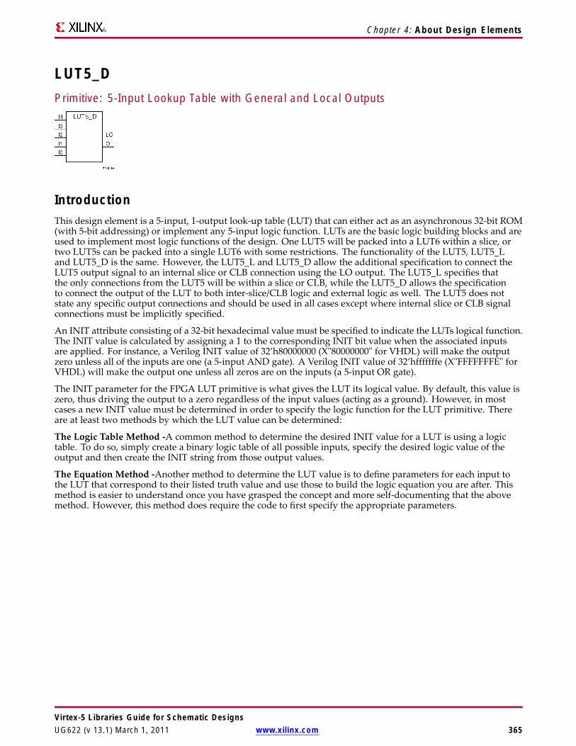
Chapter 4: About Design Elements
LUT5_DPrimitive: 5-Input Lookup Table with General and Local Outputs
IntroductionThis design element is a 5-input, 1-output look-up table (LUT) that can either act as an asynchronous 32-bit ROM(with 5-bit addressing) or implement any 5-input logic function. LUTs are the basic logic building blocks and areused to implement most logic functions of the design. One LUT5 will be packed into a LUT6 within a slice, ortwo LUT5s can be packed into a single LUT6 with some restrictions. The functionality of the LUT5, LUT5_Land LUT5_D is the same. However, the LUT5_L and LUT5_D allow the additional specification to connect theLUT5 output signal to an internal slice or CLB connection using the LO output. The LUT5_L specifies thatthe only connections from the LUT5 will be within a slice or CLB, while the LUT5_D allows the specificationto connect the output of the LUT to both inter-slice/CLB logic and external logic as well. The LUT5 does notstate any specific output connections and should be used in all cases except where internal slice or CLB signalconnections must be implicitly specified.
An INIT attribute consisting of a 32-bit hexadecimal value must be specified to indicate the LUTs logical function.The INIT value is calculated by assigning a 1 to the corresponding INIT bit value when the associated inputsare applied. For instance, a Verilog INIT value of 32’h80000000 (X"80000000" for VHDL) will make the outputzero unless all of the inputs are one (a 5-input AND gate). A Verilog INIT value of 32’hfffffffe (X"FFFFFFFE" forVHDL) will make the output one unless all zeros are on the inputs (a 5-input OR gate).
The INIT parameter for the FPGA LUT primitive is what gives the LUT its logical value. By default, this value iszero, thus driving the output to a zero regardless of the input values (acting as a ground). However, in mostcases a new INIT value must be determined in order to specify the logic function for the LUT primitive. Thereare at least two methods by which the LUT value can be determined:
The Logic Table Method -A common method to determine the desired INIT value for a LUT is using a logictable. To do so, simply create a binary logic table of all possible inputs, specify the desired logic value of theoutput and then create the INIT string from those output values.
The Equation Method -Another method to determine the LUT value is to define parameters for each input tothe LUT that correspond to their listed truth value and use those to build the logic equation you are after. Thismethod is easier to understand once you have grasped the concept and more self-documenting that the abovemethod. However, this method does require the code to first specify the appropriate parameters.
Virtex-5 Libraries Guide for Schematic DesignsUG622 (v 13.1) March 1, 2011 www.xilinx.com 365
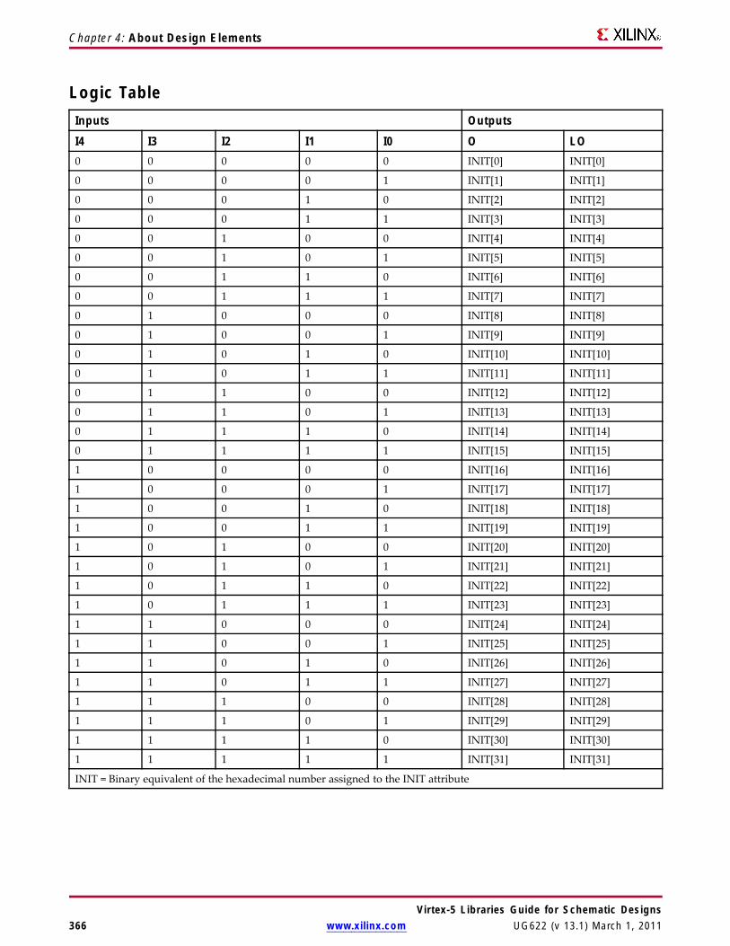
Chapter 4: About Design Elements
Logic TableInputs Outputs
I4 I3 I2 I1 I0 O LO0 0 0 0 0 INIT[0] INIT[0]
0 0 0 0 1 INIT[1] INIT[1]
0 0 0 1 0 INIT[2] INIT[2]
0 0 0 1 1 INIT[3] INIT[3]
0 0 1 0 0 INIT[4] INIT[4]
0 0 1 0 1 INIT[5] INIT[5]
0 0 1 1 0 INIT[6] INIT[6]
0 0 1 1 1 INIT[7] INIT[7]
0 1 0 0 0 INIT[8] INIT[8]
0 1 0 0 1 INIT[9] INIT[9]
0 1 0 1 0 INIT[10] INIT[10]
0 1 0 1 1 INIT[11] INIT[11]
0 1 1 0 0 INIT[12] INIT[12]
0 1 1 0 1 INIT[13] INIT[13]
0 1 1 1 0 INIT[14] INIT[14]
0 1 1 1 1 INIT[15] INIT[15]
1 0 0 0 0 INIT[16] INIT[16]
1 0 0 0 1 INIT[17] INIT[17]
1 0 0 1 0 INIT[18] INIT[18]
1 0 0 1 1 INIT[19] INIT[19]
1 0 1 0 0 INIT[20] INIT[20]
1 0 1 0 1 INIT[21] INIT[21]
1 0 1 1 0 INIT[22] INIT[22]
1 0 1 1 1 INIT[23] INIT[23]
1 1 0 0 0 INIT[24] INIT[24]
1 1 0 0 1 INIT[25] INIT[25]
1 1 0 1 0 INIT[26] INIT[26]
1 1 0 1 1 INIT[27] INIT[27]
1 1 1 0 0 INIT[28] INIT[28]
1 1 1 0 1 INIT[29] INIT[29]
1 1 1 1 0 INIT[30] INIT[30]
1 1 1 1 1 INIT[31] INIT[31]
INIT = Binary equivalent of the hexadecimal number assigned to the INIT attribute
Virtex-5 Libraries Guide for Schematic Designs366 www.xilinx.com UG622 (v 13.1) March 1, 2011
Chapter 4: About Design Elements
Port DescriptionName Direction Width FunctionO Output 1 5-LUT output
L0 Output 1 5-LUT output for internal CLB connection
I0, I1, I2, I3, I4 Input 1 LUT inputs
Design Entry MethodThis design element can be used in schematics.
Available Attributes
Attribute TypeAllowedValues Default Description
INIT Hexadecimal Any 32-Bit Value All zeros Specifies the logic value for the look-uptables.
For More Information• See the Virtex-5 FPGA User Guide.
• See the Virtex-5 FPGA Data Sheet DC and Switching Characteristics.
Virtex-5 Libraries Guide for Schematic DesignsUG622 (v 13.1) March 1, 2011 www.xilinx.com 367
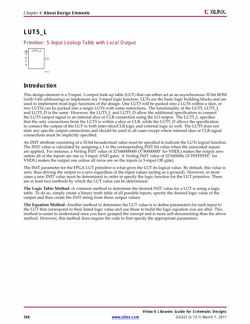
Chapter 4: About Design Elements
LUT5_LPrimitive: 5-Input Lookup Table with Local Output
IntroductionThis design element is a 5-input, 1-output look-up table (LUT) that can either act as an asynchronous 32-bit ROM(with 5-bit addressing) or implement any 5-input logic function. LUTs are the basic logic building blocks and areused to implement most logic functions of the design. One LUT5 will be packed into a LUT6 within a slice, ortwo LUT5s can be packed into a single LUT6 with some restrictions. The functionality of the LUT5, LUT5_Land LUT5_D is the same. However, the LUT5_L and LUT5_D allow the additional specification to connectthe LUT5 output signal to an internal slice or CLB connection using the LO output. The LUT5_L specifiesthat the only connections from the LUT5 is within a slice or CLB, while the LUT5_D allows the specificationto connect the output of the LUT to both inter-slice/CLB logic and external logic as well. The LUT5 does notstate any specific output connections and should be used in all cases except where internal slice or CLB signalconnections must be implicitly specified.
An INIT attribute consisting of a 32-bit hexadecimal value must be specified to indicate the LUTs logical function.The INIT value is calculated by assigning a 1 to the corresponding INIT bit value when the associated inputsare applied. For instance, a Verilog INIT value of 32’h80000000 (X"80000000" for VHDL) makes the output zerounless all of the inputs are one (a 5-input AND gate). A Verilog INIT value of 32’hfffffffe (X"FFFFFFFE" forVHDL) makes the output one unless all zeros are on the inputs (a 5-input OR gate).
The INIT parameter for the FPGA LUT primitive is what gives the LUT its logical value. By default, this value iszero, thus driving the output to a zero regardless of the input values (acting as a ground). However, in mostcases a new INIT value must be determined in order to specify the logic function for the LUT primitive. Thereare at least two methods by which the LUT value can be determined:
The Logic Table Method -A common method to determine the desired INIT value for a LUT is using a logictable. To do so, simply create a binary truth table of all possible inputs, specify the desired logic value of theoutput and then create the INIT string from those output values.
The Equation Method -Another method to determine the LUT value is to define parameters for each input tothe LUT that correspond to their listed logic value and use those to build the logic equation you are after. Thismethod is easier to understand once you have grasped the concept and is more self-documenting than the abovemethod. However, this method does require the code to first specify the appropriate parameters.
Virtex-5 Libraries Guide for Schematic Designs368 www.xilinx.com UG622 (v 13.1) March 1, 2011
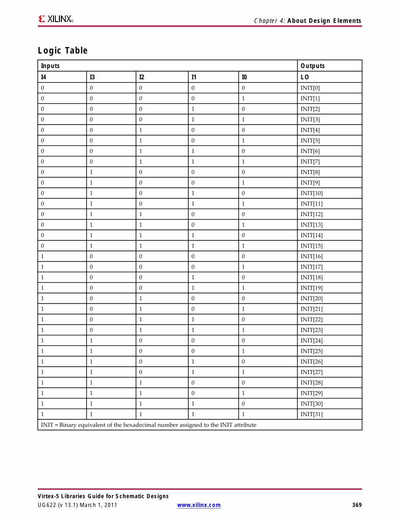
Chapter 4: About Design Elements
Logic TableInputs Outputs
I4 I3 I2 I1 I0 LO0 0 0 0 0 INIT[0]
0 0 0 0 1 INIT[1]
0 0 0 1 0 INIT[2]
0 0 0 1 1 INIT[3]
0 0 1 0 0 INIT[4]
0 0 1 0 1 INIT[5]
0 0 1 1 0 INIT[6]
0 0 1 1 1 INIT[7]
0 1 0 0 0 INIT[8]
0 1 0 0 1 INIT[9]
0 1 0 1 0 INIT[10]
0 1 0 1 1 INIT[11]
0 1 1 0 0 INIT[12]
0 1 1 0 1 INIT[13]
0 1 1 1 0 INIT[14]
0 1 1 1 1 INIT[15]
1 0 0 0 0 INIT[16]
1 0 0 0 1 INIT[17]
1 0 0 1 0 INIT[18]
1 0 0 1 1 INIT[19]
1 0 1 0 0 INIT[20]
1 0 1 0 1 INIT[21]
1 0 1 1 0 INIT[22]
1 0 1 1 1 INIT[23]
1 1 0 0 0 INIT[24]
1 1 0 0 1 INIT[25]
1 1 0 1 0 INIT[26]
1 1 0 1 1 INIT[27]
1 1 1 0 0 INIT[28]
1 1 1 0 1 INIT[29]
1 1 1 1 0 INIT[30]
1 1 1 1 1 INIT[31]
INIT = Binary equivalent of the hexadecimal number assigned to the INIT attribute
Virtex-5 Libraries Guide for Schematic DesignsUG622 (v 13.1) March 1, 2011 www.xilinx.com 369

Chapter 4: About Design Elements
Port DescriptionName Direction Width FunctionL0 Output 1 6/5-LUT output for internal CLB connection
I0, I1, I2, I3, I4 Input 1 LUT inputs
Design Entry MethodThis design element can be used in schematics.
Available Attributes
Attribute TypeAllowedValues Default Description
INIT Hexadecimal Any 32-Bit Value All zeros Specifies the logic value for the look-uptables.
For More Information• See the Virtex-5 FPGA User Guide.
• See the Virtex-5 FPGA Data Sheet DC and Switching Characteristics.
Virtex-5 Libraries Guide for Schematic Designs370 www.xilinx.com UG622 (v 13.1) March 1, 2011
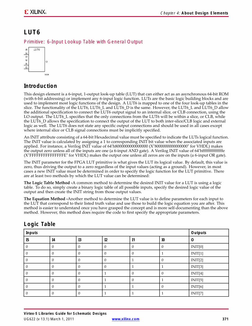
Chapter 4: About Design Elements
LUT6Primitive: 6-Input Lookup Table with General Output
IntroductionThis design element is a 6-input, 1-output look-up table (LUT) that can either act as an asynchronous 64-bit ROM(with 6-bit addressing) or implement any 6-input logic function. LUTs are the basic logic building blocks and areused to implement most logic functions of the design. A LUT6 is mapped to one of the four look-up tables in theslice. The functionality of the LUT6, LUT6_L and LUT6_D is the same. However, the LUT6_L and LUT6_D allowthe additional specification to connect the LUT6 output signal to an internal slice, or CLB connection, using theLO output. The LUT6_L specifies that the only connections from the LUT6 will be within a slice, or CLB, whilethe LUT6_D allows the specification to connect the output of the LUT to both inter-slice/CLB logic and externallogic as well. The LUT6 does not state any specific output connections and should be used in all cases exceptwhere internal slice or CLB signal connections must be implicitly specified.
An INIT attribute consisting of a 64-bit Hexadecimal value must be specified to indicate the LUTs logical function.The INIT value is calculated by assigning a 1 to corresponding INIT bit value when the associated inputs areapplied. For instance, a Verilog INIT value of 64’h8000000000000000 (X"8000000000000000" for VHDL) makesthe output zero unless all of the inputs are one (a 6-input AND gate). A Verilog INIT value of 64’hfffffffffffffffe(X"FFFFFFFFFFFFFFFE" for VHDL) makes the output one unless all zeros are on the inputs (a 6-input OR gate).
The INIT parameter for the FPGA LUT primitive is what gives the LUT its logical value. By default, this value iszero, thus driving the output to a zero regardless of the input values (acting as a ground). However, in mostcases a new INIT value must be determined in order to specify the logic function for the LUT primitive. Thereare at least two methods by which the LUT value can be determined:
The Logic Table Method -A common method to determine the desired INIT value for a LUT is using a logictable. To do so, simply create a binary logic table of all possible inputs, specify the desired logic value of theoutput and then create the INIT string from those output values.
The Equation Method -Another method to determine the LUT value is to define parameters for each input tothe LUT that correspond to their listed truth value and use those to build the logic equation you are after. Thismethod is easier to understand once you have grasped the concept and is more self-documenting than the abovemethod. However, this method does require the code to first specify the appropriate parameters.
Logic TableInputs Outputs
I5 I4 I3 I2 I1 I0 O0 0 0 0 0 0 INIT[0]
0 0 0 0 0 1 INIT[1]
0 0 0 0 1 0 INIT[2]
0 0 0 0 1 1 INIT[3]
0 0 0 1 0 0 INIT[4]
0 0 0 1 0 1 INIT[5]
0 0 0 1 1 0 INIT[6]
0 0 0 1 1 1 INIT[7]
Virtex-5 Libraries Guide for Schematic DesignsUG622 (v 13.1) March 1, 2011 www.xilinx.com 371
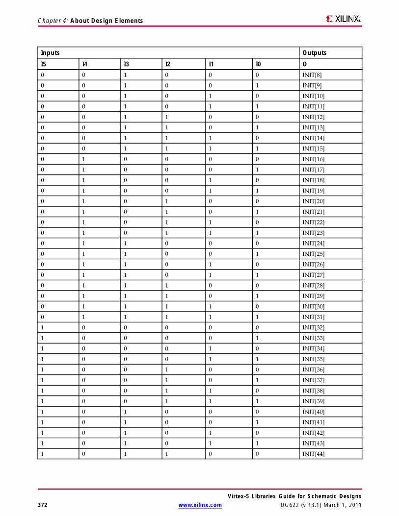
Chapter 4: About Design Elements
Inputs Outputs
I5 I4 I3 I2 I1 I0 O0 0 1 0 0 0 INIT[8]
0 0 1 0 0 1 INIT[9]
0 0 1 0 1 0 INIT[10]
0 0 1 0 1 1 INIT[11]
0 0 1 1 0 0 INIT[12]
0 0 1 1 0 1 INIT[13]
0 0 1 1 1 0 INIT[14]
0 0 1 1 1 1 INIT[15]
0 1 0 0 0 0 INIT[16]
0 1 0 0 0 1 INIT[17]
0 1 0 0 1 0 INIT[18]
0 1 0 0 1 1 INIT[19]
0 1 0 1 0 0 INIT[20]
0 1 0 1 0 1 INIT[21]
0 1 0 1 1 0 INIT[22]
0 1 0 1 1 1 INIT[23]
0 1 1 0 0 0 INIT[24]
0 1 1 0 0 1 INIT[25]
0 1 1 0 1 0 INIT[26]
0 1 1 0 1 1 INIT[27]
0 1 1 1 0 0 INIT[28]
0 1 1 1 0 1 INIT[29]
0 1 1 1 1 0 INIT[30]
0 1 1 1 1 1 INIT[31]
1 0 0 0 0 0 INIT[32]
1 0 0 0 0 1 INIT[33]
1 0 0 0 1 0 INIT[34]
1 0 0 0 1 1 INIT[35]
1 0 0 1 0 0 INIT[36]
1 0 0 1 0 1 INIT[37]
1 0 0 1 1 0 INIT[38]
1 0 0 1 1 1 INIT[39]
1 0 1 0 0 0 INIT[40]
1 0 1 0 0 1 INIT[41]
1 0 1 0 1 0 INIT[42]
1 0 1 0 1 1 INIT[43]
1 0 1 1 0 0 INIT[44]
Virtex-5 Libraries Guide for Schematic Designs372 www.xilinx.com UG622 (v 13.1) March 1, 2011

Chapter 4: About Design Elements
Inputs Outputs
I5 I4 I3 I2 I1 I0 O1 0 1 1 0 1 INIT[45]
1 0 1 1 1 0 INIT[46]
1 0 1 1 1 1 INIT[47]
1 1 0 0 0 0 INIT[48]
1 1 0 0 0 1 INIT[49]
1 1 0 0 1 0 INIT[50]
1 1 0 0 1 1 INIT[51]
1 1 0 1 0 0 INIT[52]
1 1 0 1 0 1 INIT[53]
1 1 0 1 1 0 INIT[54]
1 1 0 1 1 1 INIT[55]
1 1 1 0 0 0 INIT[56]
1 1 1 0 0 1 INIT[57]
1 1 1 0 1 0 INIT[58]
1 1 1 0 1 1 INIT[59]
1 1 1 1 0 0 INIT[60]
1 1 1 1 0 1 INIT[61]
1 1 1 1 1 0 INIT[62]
1 1 1 1 1 1 INIT[63]
INIT = Binary equivalent of the hexadecimal number assigned to the INIT attribute
Port DescriptionName Direction Width FunctionO Output 1 6/5-LUT output
I0, I1, I2, I3, I4, I5 Input 1 LUT inputs
Design Entry MethodThis design element can be used in schematics.
Available AttributesAttribute Type Allowed Values Default DescriptionINIT Hexadecimal Any 64-Bit Value All zeros Specifies the logic value for the
look-up tables.
For More Information• See the Virtex-5 FPGA User Guide.• See the Virtex-5 FPGA Data Sheet DC and Switching Characteristics.
Virtex-5 Libraries Guide for Schematic DesignsUG622 (v 13.1) March 1, 2011 www.xilinx.com 373
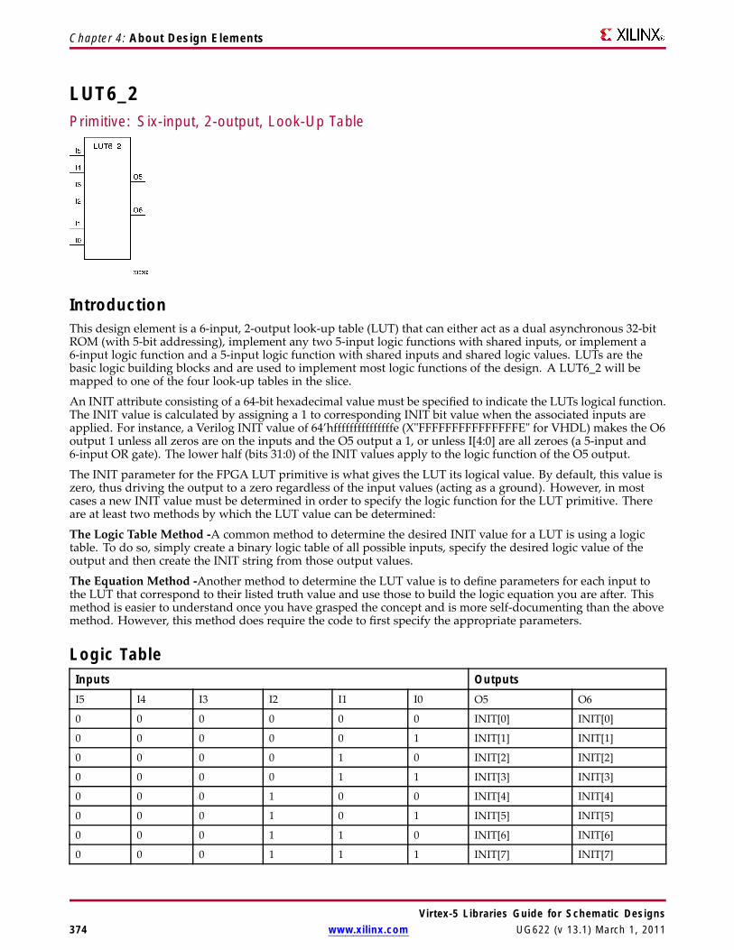
Chapter 4: About Design Elements
LUT6_2Primitive: Six-input, 2-output, Look-Up Table
IntroductionThis design element is a 6-input, 2-output look-up table (LUT) that can either act as a dual asynchronous 32-bitROM (with 5-bit addressing), implement any two 5-input logic functions with shared inputs, or implement a6-input logic function and a 5-input logic function with shared inputs and shared logic values. LUTs are thebasic logic building blocks and are used to implement most logic functions of the design. A LUT6_2 will bemapped to one of the four look-up tables in the slice.
An INIT attribute consisting of a 64-bit hexadecimal value must be specified to indicate the LUTs logical function.The INIT value is calculated by assigning a 1 to corresponding INIT bit value when the associated inputs areapplied. For instance, a Verilog INIT value of 64’hfffffffffffffffe (X"FFFFFFFFFFFFFFFE" for VHDL) makes the O6output 1 unless all zeros are on the inputs and the O5 output a 1, or unless I[4:0] are all zeroes (a 5-input and6-input OR gate). The lower half (bits 31:0) of the INIT values apply to the logic function of the O5 output.
The INIT parameter for the FPGA LUT primitive is what gives the LUT its logical value. By default, this value iszero, thus driving the output to a zero regardless of the input values (acting as a ground). However, in mostcases a new INIT value must be determined in order to specify the logic function for the LUT primitive. Thereare at least two methods by which the LUT value can be determined:
The Logic Table Method -A common method to determine the desired INIT value for a LUT is using a logictable. To do so, simply create a binary logic table of all possible inputs, specify the desired logic value of theoutput and then create the INIT string from those output values.
The Equation Method -Another method to determine the LUT value is to define parameters for each input tothe LUT that correspond to their listed truth value and use those to build the logic equation you are after. Thismethod is easier to understand once you have grasped the concept and is more self-documenting than the abovemethod. However, this method does require the code to first specify the appropriate parameters.
Logic TableInputs OutputsI5 I4 I3 I2 I1 I0 O5 O6
0 0 0 0 0 0 INIT[0] INIT[0]
0 0 0 0 0 1 INIT[1] INIT[1]
0 0 0 0 1 0 INIT[2] INIT[2]
0 0 0 0 1 1 INIT[3] INIT[3]
0 0 0 1 0 0 INIT[4] INIT[4]
0 0 0 1 0 1 INIT[5] INIT[5]
0 0 0 1 1 0 INIT[6] INIT[6]
0 0 0 1 1 1 INIT[7] INIT[7]
Virtex-5 Libraries Guide for Schematic Designs374 www.xilinx.com UG622 (v 13.1) March 1, 2011
Chapter 4: About Design Elements
Inputs Outputs0 0 1 0 0 0 INIT[8] INIT[8]
0 0 1 0 0 1 INIT[9] INIT[9]
0 0 1 0 1 0 INIT[10] INIT[10]
0 0 1 0 1 1 INIT[11] INIT[11]
0 0 1 1 0 0 INIT[12] INIT[12]
0 0 1 1 0 1 INIT[13] INIT[13]
0 0 1 1 1 0 INIT[14] INIT[14]
0 0 1 1 1 1 INIT[15] INIT[15]
0 1 0 0 0 0 INIT[16] INIT[16]
0 1 0 0 0 1 INIT[17] INIT[17]
0 1 0 0 1 0 INIT[18] INIT[18]
0 1 0 0 1 1 INIT[19] INIT[19]
0 1 0 1 0 0 INIT[20] INIT[20]
0 1 0 1 0 1 INIT[21] INIT[21]
0 1 0 1 1 0 INIT[22] INIT[22]
0 1 0 1 1 1 INIT[23] INIT[23]
0 1 1 0 0 0 INIT[24] INIT[24]
0 1 1 0 0 1 INIT[25] INIT[25]
0 1 1 0 1 0 INIT[26] INIT[26]
0 1 1 0 1 1 INIT[27] INIT[27]
0 1 1 1 0 0 INIT[28] INIT[28]
0 1 1 1 0 1 INIT[29] INIT[29]
0 1 1 1 1 0 INIT[30] INIT[30]
0 1 1 1 1 1 INIT[31] INIT[31]
1 0 0 0 0 0 INIT[0] INIT[32]
1 0 0 0 0 1 INIT[1] INIT[33]
1 0 0 0 1 0 INIT[2] INIT[34]
1 0 0 0 1 1 INIT[3] INIT[35]
1 0 0 1 0 0 INIT[4] INIT[36]
1 0 0 1 0 1 INIT[5] INIT[37]
1 0 0 1 1 0 INIT[6] INIT[38]
1 0 0 1 1 1 INIT[7] INIT[39]
1 0 1 0 0 0 INIT[8] INIT[40]
1 0 1 0 0 1 INIT[9] INIT[41]
1 0 1 0 1 0 INIT[10] INIT[42]
1 0 1 0 1 1 INIT[11] INIT[43]
1 0 1 1 0 0 INIT[12] INIT[44]
1 0 1 1 0 1 INIT[13] INIT[45]
1 0 1 1 1 0 INIT[14] INIT[46]
Virtex-5 Libraries Guide for Schematic DesignsUG622 (v 13.1) March 1, 2011 www.xilinx.com 375
Chapter 4: About Design Elements
Inputs Outputs1 0 1 1 1 1 INIT[15] INIT[47]
1 1 0 0 0 0 INIT[16] INIT[48]
1 1 0 0 0 1 INIT[17] INIT[49]
1 1 0 0 1 0 INIT[18] INIT[50]
1 1 0 0 1 1 INIT[19] INIT[51]
1 1 0 1 0 0 INIT[20] INIT[52]
1 1 0 1 0 1 INIT[21] INIT[53]
1 1 0 1 1 0 INIT[22] INIT[54]
1 1 0 1 1 1 INIT[23] INIT[55]
1 1 1 0 0 0 INIT[24] INIT[56]
1 1 1 0 0 1 INIT[25] INIT[57]
1 1 1 0 1 0 INIT[26] INIT[58]
1 1 1 0 1 1 INIT[27] INIT[59]
1 1 1 1 0 0 INIT[28] INIT[60]
1 1 1 1 0 1 INIT[29] INIT[61]
1 1 1 1 1 0 INIT[30] INIT[62]
1 1 1 1 1 1 INIT[31] INIT[63]
INIT = Binary equivalent of the hexadecimal number assigned to the INIT attribute
Port DescriptionsPort Direction Width FunctionO6 Output 1 6/5-LUT output
O5 Output 1 5-LUT output
I0, I1, I2, I3, I4, I5 Input 1 LUT inputs
Design Entry MethodThis design element can be used in schematics.
Available AttributesAttribute Type Allowed Values Default DescriptionINIT Hexadecimal Any 64-Bit Value All zeros Specifies the LUT5/6 output function.
For More Information• See the Virtex-5 FPGA User Guide.
• See the Virtex-5 FPGA Data Sheet DC and Switching Characteristics.
Virtex-5 Libraries Guide for Schematic Designs376 www.xilinx.com UG622 (v 13.1) March 1, 2011
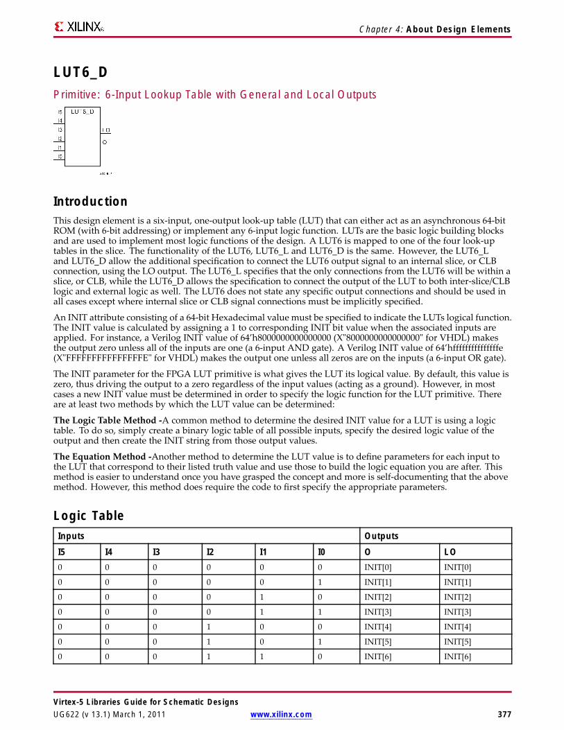
Chapter 4: About Design Elements
LUT6_DPrimitive: 6-Input Lookup Table with General and Local Outputs
IntroductionThis design element is a six-input, one-output look-up table (LUT) that can either act as an asynchronous 64-bitROM (with 6-bit addressing) or implement any 6-input logic function. LUTs are the basic logic building blocksand are used to implement most logic functions of the design. A LUT6 is mapped to one of the four look-uptables in the slice. The functionality of the LUT6, LUT6_L and LUT6_D is the same. However, the LUT6_Land LUT6_D allow the additional specification to connect the LUT6 output signal to an internal slice, or CLBconnection, using the LO output. The LUT6_L specifies that the only connections from the LUT6 will be within aslice, or CLB, while the LUT6_D allows the specification to connect the output of the LUT to both inter-slice/CLBlogic and external logic as well. The LUT6 does not state any specific output connections and should be used inall cases except where internal slice or CLB signal connections must be implicitly specified.
An INIT attribute consisting of a 64-bit Hexadecimal value must be specified to indicate the LUTs logical function.The INIT value is calculated by assigning a 1 to corresponding INIT bit value when the associated inputs areapplied. For instance, a Verilog INIT value of 64’h8000000000000000 (X"8000000000000000" for VHDL) makesthe output zero unless all of the inputs are one (a 6-input AND gate). A Verilog INIT value of 64’hfffffffffffffffe(X"FFFFFFFFFFFFFFFE" for VHDL) makes the output one unless all zeros are on the inputs (a 6-input OR gate).
The INIT parameter for the FPGA LUT primitive is what gives the LUT its logical value. By default, this value iszero, thus driving the output to a zero regardless of the input values (acting as a ground). However, in mostcases a new INIT value must be determined in order to specify the logic function for the LUT primitive. Thereare at least two methods by which the LUT value can be determined:
The Logic Table Method -A common method to determine the desired INIT value for a LUT is using a logictable. To do so, simply create a binary logic table of all possible inputs, specify the desired logic value of theoutput and then create the INIT string from those output values.
The Equation Method -Another method to determine the LUT value is to define parameters for each input tothe LUT that correspond to their listed truth value and use those to build the logic equation you are after. Thismethod is easier to understand once you have grasped the concept and more is self-documenting that the abovemethod. However, this method does require the code to first specify the appropriate parameters.
Logic TableInputs Outputs
I5 I4 I3 I2 I1 I0 O LO0 0 0 0 0 0 INIT[0] INIT[0]
0 0 0 0 0 1 INIT[1] INIT[1]
0 0 0 0 1 0 INIT[2] INIT[2]
0 0 0 0 1 1 INIT[3] INIT[3]
0 0 0 1 0 0 INIT[4] INIT[4]
0 0 0 1 0 1 INIT[5] INIT[5]
0 0 0 1 1 0 INIT[6] INIT[6]
Virtex-5 Libraries Guide for Schematic DesignsUG622 (v 13.1) March 1, 2011 www.xilinx.com 377

Chapter 4: About Design Elements
Inputs Outputs
I5 I4 I3 I2 I1 I0 O LO0 0 0 1 1 1 INIT[7] INIT[7]
0 0 1 0 0 0 INIT[8] INIT[8]
0 0 1 0 0 1 INIT[9] INIT[9]
0 0 1 0 1 0 INIT[10] INIT[10]
0 0 1 0 1 1 INIT[11] INIT[11]
0 0 1 1 0 0 INIT[12] INIT[12]
0 0 1 1 0 1 INIT[13] INIT[13]
0 0 1 1 1 0 INIT[14] INIT[14]
0 0 1 1 1 1 INIT[15] INIT[15]
0 1 0 0 0 0 INIT[16] INIT[16]
0 1 0 0 0 1 INIT[17] INIT[17]
0 1 0 0 1 0 INIT[18] INIT[18]
0 1 0 0 1 1 INIT[19] INIT[19]
0 1 0 1 0 0 INIT[20] INIT[20]
0 1 0 1 0 1 INIT[21] INIT[21]
0 1 0 1 1 0 INIT[22] INIT[22]
0 1 0 1 1 1 INIT[23] INIT[23]
0 1 1 0 0 0 INIT[24] INIT[24]
0 1 1 0 0 1 INIT[25] INIT[25]
0 1 1 0 1 0 INIT[26] INIT[26]
0 1 1 0 1 1 INIT[27] INIT[27]
0 1 1 1 0 0 INIT[28] INIT[28]
0 1 1 1 0 1 INIT[29] INIT[29]
0 1 1 1 1 0 INIT[30] INIT[30]
0 1 1 1 1 1 INIT[31] INIT[31]
1 0 0 0 0 0 INIT[32] INIT[32]
1 0 0 0 0 1 INIT[33] INIT[33]
1 0 0 0 1 0 INIT[34] INIT[34]
1 0 0 0 1 1 INIT[35] INIT[35]
1 0 0 1 0 0 INIT[36] INIT[36]
1 0 0 1 0 1 INIT[37] INIT[37]
1 0 0 1 1 0 INIT[38] INIT[38]
1 0 0 1 1 1 INIT[39] INIT[39]
1 0 1 0 0 0 INIT[40] INIT[40]
1 0 1 0 0 1 INIT[41] INIT[41]
1 0 1 0 1 0 INIT[42] INIT[42]
1 0 1 0 1 1 INIT[43] INIT[43]
Virtex-5 Libraries Guide for Schematic Designs378 www.xilinx.com UG622 (v 13.1) March 1, 2011
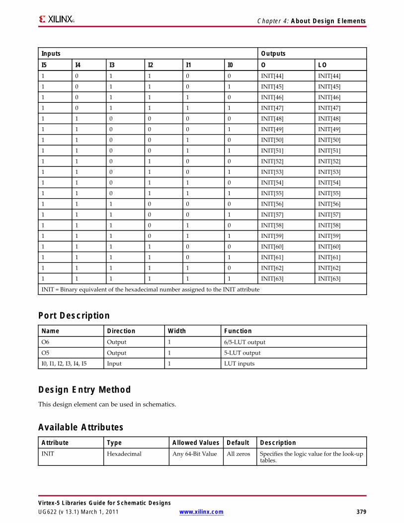
Chapter 4: About Design Elements
Inputs Outputs
I5 I4 I3 I2 I1 I0 O LO1 0 1 1 0 0 INIT[44] INIT[44]
1 0 1 1 0 1 INIT[45] INIT[45]
1 0 1 1 1 0 INIT[46] INIT[46]
1 0 1 1 1 1 INIT[47] INIT[47]
1 1 0 0 0 0 INIT[48] INIT[48]
1 1 0 0 0 1 INIT[49] INIT[49]
1 1 0 0 1 0 INIT[50] INIT[50]
1 1 0 0 1 1 INIT[51] INIT[51]
1 1 0 1 0 0 INIT[52] INIT[52]
1 1 0 1 0 1 INIT[53] INIT[53]
1 1 0 1 1 0 INIT[54] INIT[54]
1 1 0 1 1 1 INIT[55] INIT[55]
1 1 1 0 0 0 INIT[56] INIT[56]
1 1 1 0 0 1 INIT[57] INIT[57]
1 1 1 0 1 0 INIT[58] INIT[58]
1 1 1 0 1 1 INIT[59] INIT[59]
1 1 1 1 0 0 INIT[60] INIT[60]
1 1 1 1 0 1 INIT[61] INIT[61]
1 1 1 1 1 0 INIT[62] INIT[62]
1 1 1 1 1 1 INIT[63] INIT[63]
INIT = Binary equivalent of the hexadecimal number assigned to the INIT attribute
Port DescriptionName Direction Width FunctionO6 Output 1 6/5-LUT output
O5 Output 1 5-LUT output
I0, I1, I2, I3, I4, I5 Input 1 LUT inputs
Design Entry MethodThis design element can be used in schematics.
Available AttributesAttribute Type Allowed Values Default DescriptionINIT Hexadecimal Any 64-Bit Value All zeros Specifies the logic value for the look-up
tables.
Virtex-5 Libraries Guide for Schematic DesignsUG622 (v 13.1) March 1, 2011 www.xilinx.com 379

Chapter 4: About Design Elements
For More Information• See the Virtex-5 FPGA User Guide.
• See the Virtex-5 FPGA Data Sheet DC and Switching Characteristics.
Virtex-5 Libraries Guide for Schematic Designs380 www.xilinx.com UG622 (v 13.1) March 1, 2011

Chapter 4: About Design Elements
LUT6_LPrimitive: 6-Input Lookup Table with Local Output
IntroductionThis design element is a 6-input, 1-output look-up table (LUT) that can either act as an asynchronous 64-bit ROM(with 6-bit addressing) or implement any 6-input logic function. LUTs are the basic logic building blocks and areused to implement most logic functions of the design. A LUT6 is mapped to one of the four look-up tables inthe slice. The functionality of the LUT6, LUT6_L and LUT6_D is the same. However, the LUT6_L and LUT6_Dallow the additional specification to connect the LUT6 output signal to an internal slice, or CLB connection, usingthe LO output. The LUT6_L specifies that the only connections from the LUT6 are within a slice, or CLB, whilethe LUT6_D allows the specification to connect the output of the LUT to both inter-slice/CLB logic and externallogic as well. The LUT6 does not state any specific output connections and should be used in all cases exceptwhere internal slice or CLB signal connections must be implicitly specified.
An INIT attribute consisting of a 64-bit hexadecimal value must be specified to indicate the LUT’s logicalfunction. The INIT value is calculated by assigning a 1 to the corresponding INIT bit value when the associatedinputs are applied. For instance, a Verilog INIT value of 64’h8000000000000000 (X"8000000000000000" forVHDL) will make the output zero unless all of the inputs are one (a 6-input AND gate). A Verilog INIT valueof 64’hfffffffffffffffe (X"FFFFFFFFFFFFFFFE" for VHDL) will make the output one unless all zeros are on theinputs (a 6-input OR gate).
The INIT parameter for the FPGA LUT primitive is what gives the LUT its logical value. By default, this value iszero, thus driving the output to a zero regardless of the input values (acting as a ground). However, in mostcases a new INIT value must be determined in order to specify the logic function for the LUT primitive. Thereare at least two methods by which the LUT value can be determined:
The Logic Table Method -A common method to determine the desired INIT value for a LUT is using a logictable. To do so, simply create a binary truth table of all possible inputs, specify the desired logic value of theoutput and then create the INIT string from those output values.
The Equation Method -Another method to determine the LUT value is to define parameters for each input tothe LUT that correspond to their listed truth value and use those to build the logic equation you are after. Thismethod is easier to understand once you have grasped the concept and is more self-documenting that the abovemethod. However, this method does require the code to first specify the appropriate parameters.
Logic TableInputs Outputs
I5 I4 I3 I2 I1 I0 LO0 0 0 0 0 0 INIT[0]
0 0 0 0 0 1 INIT[1]
0 0 0 0 1 0 INIT[2]
0 0 0 0 1 1 INIT[3]
0 0 0 1 0 0 INIT[4]
0 0 0 1 0 1 INIT[5]
0 0 0 1 1 0 INIT[6]
Virtex-5 Libraries Guide for Schematic DesignsUG622 (v 13.1) March 1, 2011 www.xilinx.com 381

Chapter 4: About Design Elements
Inputs Outputs
I5 I4 I3 I2 I1 I0 LO0 0 0 1 1 1 INIT[7]
0 0 1 0 0 0 INIT[8]
0 0 1 0 0 1 INIT[9]
0 0 1 0 1 0 INIT[10]
0 0 1 0 1 1 INIT[11]
0 0 1 1 0 0 INIT[12]
0 0 1 1 0 1 INIT[13]
0 0 1 1 1 0 INIT[14]
0 0 1 1 1 1 INIT[15]
0 1 0 0 0 0 INIT[16]
0 1 0 0 0 1 INIT[17]
0 1 0 0 1 0 INIT[18]
0 1 0 0 1 1 INIT[19]
0 1 0 1 0 0 INIT[20]
0 1 0 1 0 1 INIT[21]
0 1 0 1 1 0 INIT[22]
0 1 0 1 1 1 INIT[23]
0 1 1 0 0 0 INIT[24]
0 1 1 0 0 1 INIT[25]
0 1 1 0 1 0 INIT[26]
0 1 1 0 1 1 INIT[27]
0 1 1 1 0 0 INIT[28]
0 1 1 1 0 1 INIT[29]
0 1 1 1 1 0 INIT[30]
0 1 1 1 1 1 INIT[31]
1 0 0 0 0 0 INIT[32]
1 0 0 0 0 1 INIT[33]
1 0 0 0 1 0 INIT[34]
1 0 0 0 1 1 INIT[35]
1 0 0 1 0 0 INIT[36]
1 0 0 1 0 1 INIT[37]
1 0 0 1 1 0 INIT[38]
1 0 0 1 1 1 INIT[39]
1 0 1 0 0 0 INIT[40]
1 0 1 0 0 1 INIT[41]
1 0 1 0 1 0 INIT[42]
1 0 1 0 1 1 INIT[43]
Virtex-5 Libraries Guide for Schematic Designs382 www.xilinx.com UG622 (v 13.1) March 1, 2011
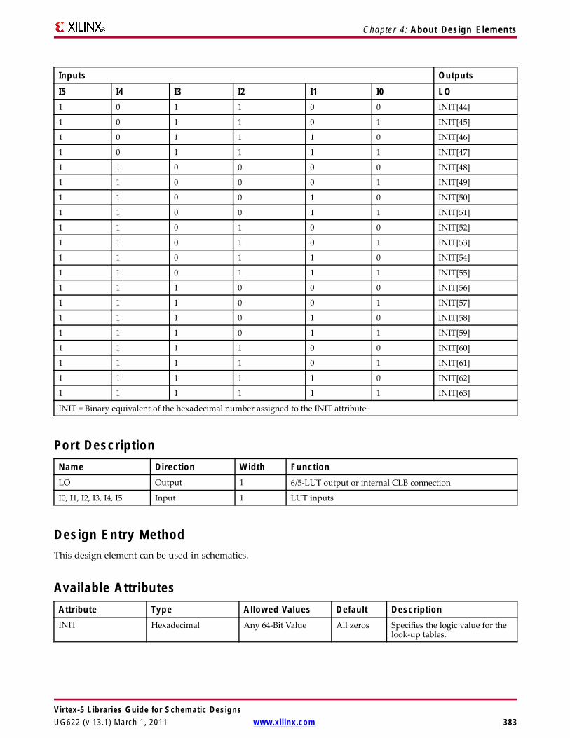
Chapter 4: About Design Elements
Inputs Outputs
I5 I4 I3 I2 I1 I0 LO1 0 1 1 0 0 INIT[44]
1 0 1 1 0 1 INIT[45]
1 0 1 1 1 0 INIT[46]
1 0 1 1 1 1 INIT[47]
1 1 0 0 0 0 INIT[48]
1 1 0 0 0 1 INIT[49]
1 1 0 0 1 0 INIT[50]
1 1 0 0 1 1 INIT[51]
1 1 0 1 0 0 INIT[52]
1 1 0 1 0 1 INIT[53]
1 1 0 1 1 0 INIT[54]
1 1 0 1 1 1 INIT[55]
1 1 1 0 0 0 INIT[56]
1 1 1 0 0 1 INIT[57]
1 1 1 0 1 0 INIT[58]
1 1 1 0 1 1 INIT[59]
1 1 1 1 0 0 INIT[60]
1 1 1 1 0 1 INIT[61]
1 1 1 1 1 0 INIT[62]
1 1 1 1 1 1 INIT[63]
INIT = Binary equivalent of the hexadecimal number assigned to the INIT attribute
Port DescriptionName Direction Width FunctionLO Output 1 6/5-LUT output or internal CLB connection
I0, I1, I2, I3, I4, I5 Input 1 LUT inputs
Design Entry MethodThis design element can be used in schematics.
Available AttributesAttribute Type Allowed Values Default DescriptionINIT Hexadecimal Any 64-Bit Value All zeros Specifies the logic value for the
look-up tables.
Virtex-5 Libraries Guide for Schematic DesignsUG622 (v 13.1) March 1, 2011 www.xilinx.com 383

Chapter 4: About Design Elements
For More Information• See the Virtex-5 FPGA User Guide.
• See the Virtex-5 FPGA Data Sheet DC and Switching Characteristics.
Virtex-5 Libraries Guide for Schematic Designs384 www.xilinx.com UG622 (v 13.1) March 1, 2011

Chapter 4: About Design Elements
M16_1EMacro: 16-to-1 Multiplexer with Enable
IntroductionThis design element is a 16-to-1 multiplexer with enable. When the enable input (E) is High, the M16_1Emultiplexer chooses one data bit from 16 sources (D15 : D0) under the control of the select inputs (S3 : S0). Theoutput (O) reflects the state of the selected input as shown in the logic table. When (E) is Low, the output is Low.
Virtex-5 Libraries Guide for Schematic DesignsUG622 (v 13.1) March 1, 2011 www.xilinx.com 385

Chapter 4: About Design Elements
Logic TableInputs Outputs
E S3 S2 S1 S0 D15-D0 O0 X X X X X 0
1 0 0 0 0 D0 D0
1 0 0 0 1 D1 D1
1 0 0 1 0 D2 D2
1 0 0 1 1 D3 D3...
.
.
.
.
.
.
.
.
.
.
.
.
.
.
.
.
.
.
1 1 1 0 0 D12 D12
1 1 1 0 1 D13 D13
1 1 1 1 0 D14 D14
1 1 1 1 1 D15 D15
Design Entry MethodThis design element is only for use in schematics.
For More Information• See the Virtex-5 FPGA User Guide.
• See the Virtex-5 FPGA Data Sheet DC and Switching Characteristics.
Virtex-5 Libraries Guide for Schematic Designs386 www.xilinx.com UG622 (v 13.1) March 1, 2011

Chapter 4: About Design Elements
M2_1Macro: 2-to-1 Multiplexer
IntroductionThis design element chooses one data bit from two sources (D1 or D0) under the control of the select input (S0).The output (O) reflects the state of the selected data input. When Low, S0 selects D0 and when High, S0 selects D1.
Logic TableInputs Outputs
S0 D1 D0 O1 D1 X D1
0 X D0 D0
Design Entry MethodThis design element is only for use in schematics.
For More Information• See the Virtex-5 FPGA User Guide.
• See the Virtex-5 FPGA Data Sheet DC and Switching Characteristics.
Virtex-5 Libraries Guide for Schematic DesignsUG622 (v 13.1) March 1, 2011 www.xilinx.com 387

Chapter 4: About Design Elements
M2_1B1Macro: 2-to-1 Multiplexer with D0 Inverted
IntroductionThis design element chooses one data bit from two sources (D1 or D0) under the control of select input (S0).When S0 is Low, the output (O) reflects the inverted value of (D0). When S0 is High, (O) reflects the state of D1.
Logic TableInputs Outputs
S0 D1 D0 O1 1 X 1
1 0 X 0
0 X 1 0
0 X 0 1
Design Entry MethodThis design element is only for use in schematics.
For More Information• See the Virtex-5 FPGA User Guide.
• See the Virtex-5 FPGA Data Sheet DC and Switching Characteristics.
Virtex-5 Libraries Guide for Schematic Designs388 www.xilinx.com UG622 (v 13.1) March 1, 2011

Chapter 4: About Design Elements
M2_1B2Macro: 2-to-1 Multiplexer with D0 and D1 Inverted
IntroductionThis design element chooses one data bit from two sources (D1 or D0) under the control of select input (S0). WhenS0 is Low, the output (O) reflects the inverted value of D0. When S0 is High, O reflects the inverted value of D1.
Logic TableInputs Outputs
S0 D1 D0 O1 1 X 0
1 0 X 1
0 X 1 0
0 X 0 1
Design Entry MethodThis design element is only for use in schematics.
For More Information• See the Virtex-5 FPGA User Guide.
• See the Virtex-5 FPGA Data Sheet DC and Switching Characteristics.
Virtex-5 Libraries Guide for Schematic DesignsUG622 (v 13.1) March 1, 2011 www.xilinx.com 389

Chapter 4: About Design Elements
M2_1EMacro: 2-to-1 Multiplexer with Enable
IntroductionThis design element is a 2-to-1 multiplexer with enable. When the enable input (E) is High, the M2_1E choosesone data bit from two sources (D1 or D0) under the control of select input (S0). When Low, S0 selects D0 andwhen High, S0 selects D1. When (E) is Low, the output is Low.
Logic TableInputs Outputs
E S0 D1 D0 O0 X X X 0
1 0 X 1 1
1 0 X 0 0
1 1 1 X 1
1 1 0 X 0
Design Entry MethodThis design element is only for use in schematics.
For More Information• See the Virtex-5 FPGA User Guide.
• See the Virtex-5 FPGA Data Sheet DC and Switching Characteristics.
Virtex-5 Libraries Guide for Schematic Designs390 www.xilinx.com UG622 (v 13.1) March 1, 2011

Chapter 4: About Design Elements
M4_1EMacro: 4-to-1 Multiplexer with Enable
IntroductionThis design element is a 4-to-1 multiplexer with enable. When the enable input (E) is High, the M4_1Emultiplexerchooses one data bit from four sources (D3, D2, D1, or D0) under the control of the select inputs (S1 : S0). Theoutput (O) reflects the state of the selected input as shown in the logic table. When (E) is Low, the output is Low.
Logic TableInputs Outputs
E S1 S0 D0 D1 D2 D3 O0 X X X X X X 0
1 0 0 D0 X X X D0
1 0 1 X D1 X X D1
1 1 0 X X D2 X D2
1 1 1 X X X D3 D3
Design Entry MethodThis design element is only for use in schematics.
For More Information• See the Virtex-5 FPGA User Guide.
• See the Virtex-5 FPGA Data Sheet DC and Switching Characteristics.
Virtex-5 Libraries Guide for Schematic DesignsUG622 (v 13.1) March 1, 2011 www.xilinx.com 391
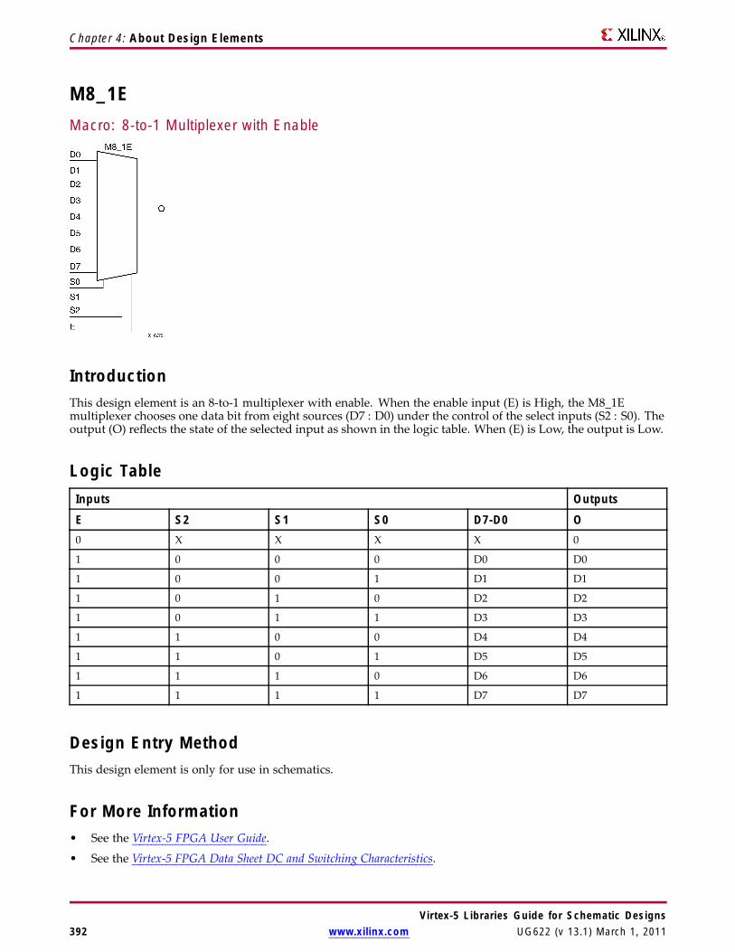
Chapter 4: About Design Elements
M8_1EMacro: 8-to-1 Multiplexer with Enable
IntroductionThis design element is an 8-to-1 multiplexer with enable. When the enable input (E) is High, the M8_1Emultiplexer chooses one data bit from eight sources (D7 : D0) under the control of the select inputs (S2 : S0). Theoutput (O) reflects the state of the selected input as shown in the logic table. When (E) is Low, the output is Low.
Logic TableInputs Outputs
E S2 S1 S0 D7-D0 O0 X X X X 0
1 0 0 0 D0 D0
1 0 0 1 D1 D1
1 0 1 0 D2 D2
1 0 1 1 D3 D3
1 1 0 0 D4 D4
1 1 0 1 D5 D5
1 1 1 0 D6 D6
1 1 1 1 D7 D7
Design Entry MethodThis design element is only for use in schematics.
For More Information• See the Virtex-5 FPGA User Guide.
• See the Virtex-5 FPGA Data Sheet DC and Switching Characteristics.
Virtex-5 Libraries Guide for Schematic Designs392 www.xilinx.com UG622 (v 13.1) March 1, 2011

Chapter 4: About Design Elements
MULT18X18Primitive: 18 x 18 Signed Multiplier
IntroductionMULT18X18 is a combinational signed 18-bit by 18-bit multiplier. The value represented in the 18-bit input A ismultiplied by the value represented in the 18-bit input B. Output P is the 36-bit product of A and B.
Logic TableInputs OutputA B PA B A x B
A, B, and P are two’s complement.
Design Entry MethodThis design element can be used in schematics.
For More Information• See the Virtex-5 FPGA User Guide.
• See the Virtex-5 FPGA Data Sheet DC and Switching Characteristics.
Virtex-5 Libraries Guide for Schematic DesignsUG622 (v 13.1) March 1, 2011 www.xilinx.com 393
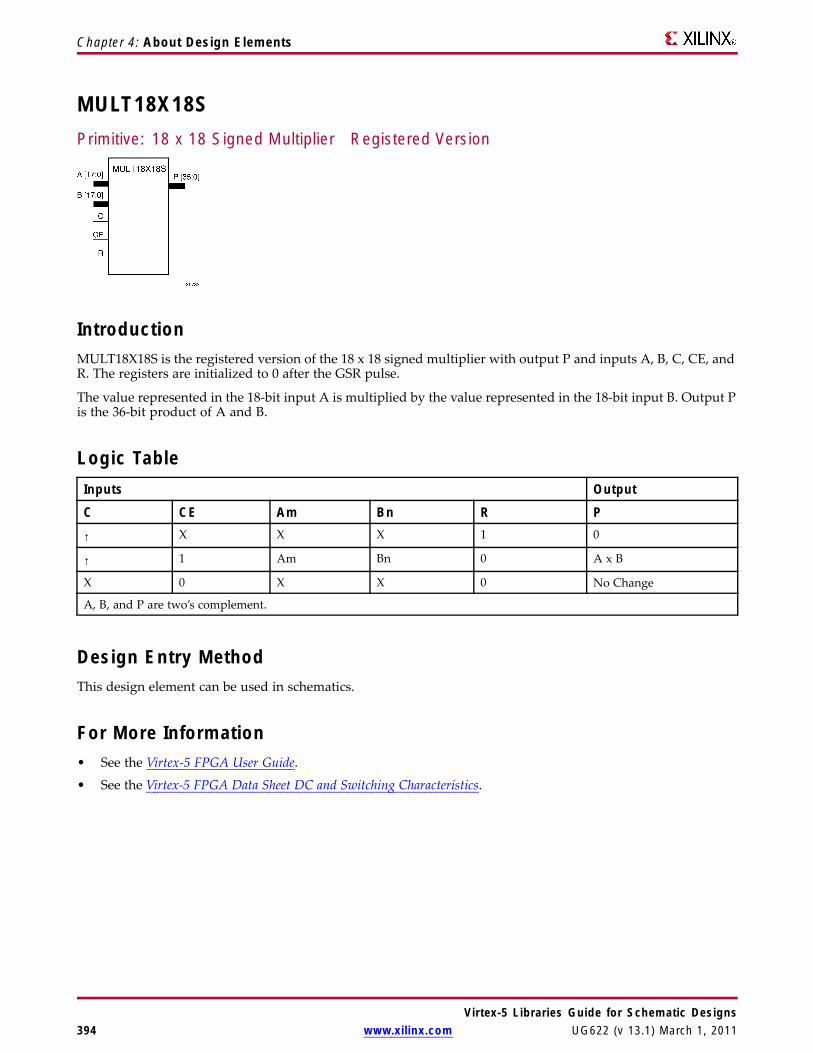
Chapter 4: About Design Elements
MULT18X18SPrimitive: 18 x 18 Signed Multiplier Registered Version
IntroductionMULT18X18S is the registered version of the 18 x 18 signed multiplier with output P and inputs A, B, C, CE, andR. The registers are initialized to 0 after the GSR pulse.
The value represented in the 18-bit input A is multiplied by the value represented in the 18-bit input B. Output Pis the 36-bit product of A and B.
Logic TableInputs Output
C CE Am Bn R P
↑ X X X 1 0
↑ 1 Am Bn 0 A x B
X 0 X X 0 No Change
A, B, and P are two’s complement.
Design Entry MethodThis design element can be used in schematics.
For More Information• See the Virtex-5 FPGA User Guide.
• See the Virtex-5 FPGA Data Sheet DC and Switching Characteristics.
Virtex-5 Libraries Guide for Schematic Designs394 www.xilinx.com UG622 (v 13.1) March 1, 2011
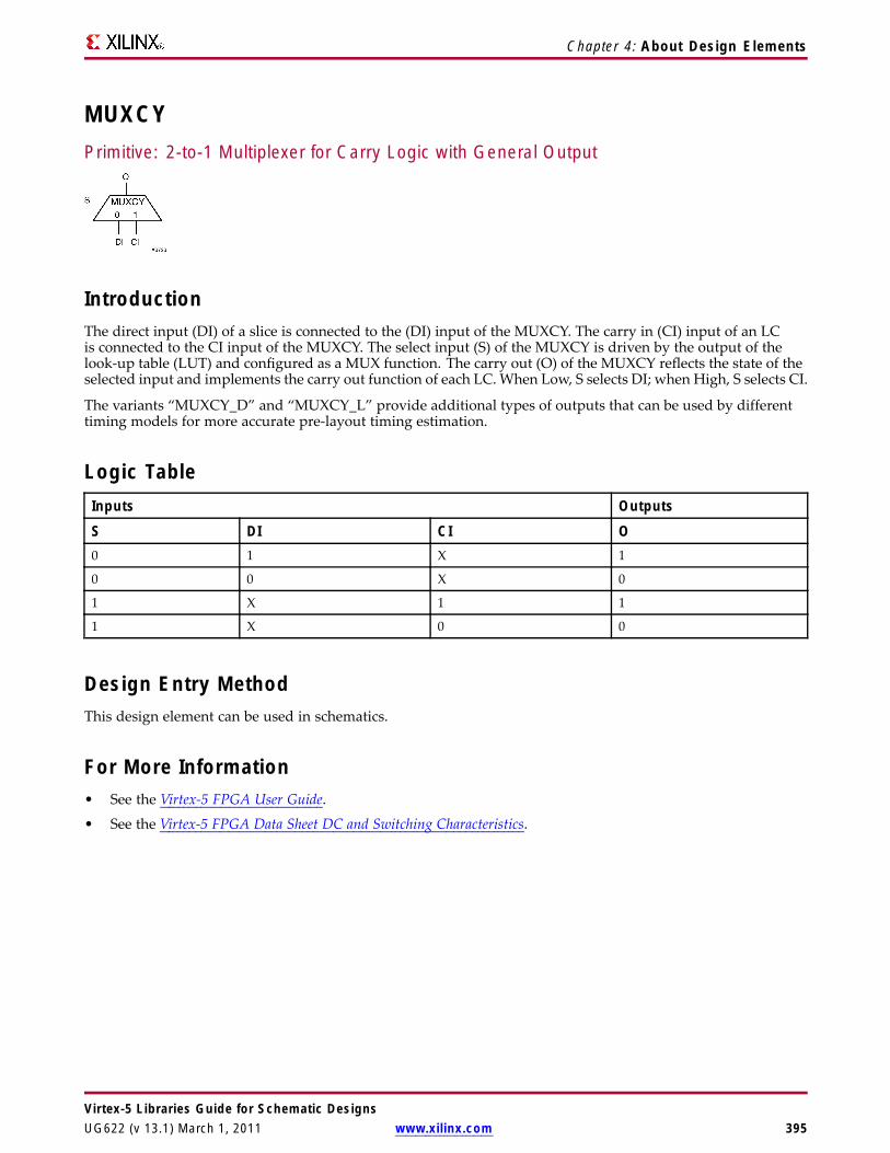
Chapter 4: About Design Elements
MUXCYPrimitive: 2-to-1 Multiplexer for Carry Logic with General Output
IntroductionThe direct input (DI) of a slice is connected to the (DI) input of the MUXCY. The carry in (CI) input of an LCis connected to the CI input of the MUXCY. The select input (S) of the MUXCY is driven by the output of thelook-up table (LUT) and configured as a MUX function. The carry out (O) of the MUXCY reflects the state of theselected input and implements the carry out function of each LC. When Low, S selects DI; when High, S selects CI.
The variants “MUXCY_D” and “MUXCY_L” provide additional types of outputs that can be used by differenttiming models for more accurate pre-layout timing estimation.
Logic TableInputs Outputs
S DI CI O0 1 X 1
0 0 X 0
1 X 1 1
1 X 0 0
Design Entry MethodThis design element can be used in schematics.
For More Information• See the Virtex-5 FPGA User Guide.
• See the Virtex-5 FPGA Data Sheet DC and Switching Characteristics.
Virtex-5 Libraries Guide for Schematic DesignsUG622 (v 13.1) March 1, 2011 www.xilinx.com 395
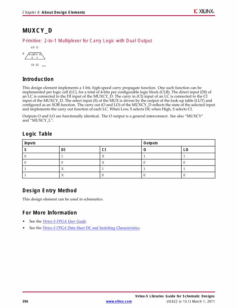
Chapter 4: About Design Elements
MUXCY_DPrimitive: 2-to-1 Multiplexer for Carry Logic with Dual Output
IntroductionThis design element implements a 1-bit, high-speed carry propagate function. One such function can beimplemented per logic cell (LC), for a total of 4-bits per configurable logic block (CLB). The direct input (DI) ofan LC is connected to the DI input of the MUXCY_D. The carry in (CI) input of an LC is connected to the CIinput of the MUXCY_D. The select input (S) of the MUX is driven by the output of the look-up table (LUT) andconfigured as an XOR function. The carry out (O and LO) of the MUXCY_D reflects the state of the selected inputand implements the carry out function of each LC. When Low, S selects DI; when High, S selects CI.
Outputs O and LO are functionally identical. The O output is a general interconnect. See also “MUXCY”and “MUXCY_L”.
Logic TableInputs Outputs
S DI CI O LO0 1 X 1 1
0 0 X 0 0
1 X 1 1 1
1 X 0 0 0
Design Entry MethodThis design element can be used in schematics.
For More Information• See the Virtex-5 FPGA User Guide.
• See the Virtex-5 FPGA Data Sheet DC and Switching Characteristics.
Virtex-5 Libraries Guide for Schematic Designs396 www.xilinx.com UG622 (v 13.1) March 1, 2011
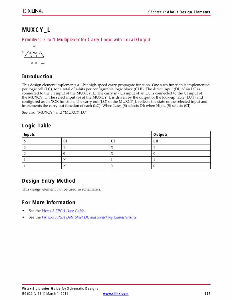
Chapter 4: About Design Elements
MUXCY_LPrimitive: 2-to-1 Multiplexer for Carry Logic with Local Output
IntroductionThis design element implements a 1-bit high-speed carry propagate function. One such function is implementedper logic cell (LC), for a total of 4-bits per configurable logic block (CLB). The direct input (DI) of an LC isconnected to the DI input of the MUXCY_L. The carry in (CI) input of an LC is connected to the CI input ofthe MUXCY_L. The select input (S) of the MUXCY_L is driven by the output of the look-up table (LUT) andconfigured as an XOR function. The carry out (LO) of the MUXCY_L reflects the state of the selected input andimplements the carry out function of each (LC). When Low, (S) selects DI; when High, (S) selects (CI).
See also “MUXCY” and “MUXCY_D.”
Logic TableInputs Outputs
S DI CI LO0 1 X 1
0 0 X 0
1 X 1 1
1 X 0 0
Design Entry MethodThis design element can be used in schematics.
For More Information• See the Virtex-5 FPGA User Guide.
• See the Virtex-5 FPGA Data Sheet DC and Switching Characteristics.
Virtex-5 Libraries Guide for Schematic DesignsUG622 (v 13.1) March 1, 2011 www.xilinx.com 397
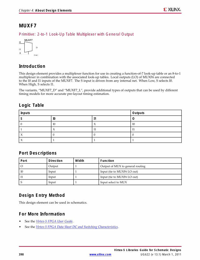
Chapter 4: About Design Elements
MUXF7Primitive: 2-to-1 Look-Up Table Multiplexer with General Output
IntroductionThis design element provides a multiplexer function for use in creating a function-of-7 look-up table or an 8-to-1multiplexer in combination with the associated look-up tables. Local outputs (LO) of MUXF6 are connectedto the I0 and I1 inputs of the MUXF7. The S input is driven from any internal net. When Low, S selects I0.When High, S selects I1.
The variants, “MUXF7_D” and “MUXF7_L”, provide additional types of outputs that can be used by differenttiming models for more accurate pre-layout timing estimation.
Logic TableInputs Outputs
S I0 I1 O0 I0 X I0
1 X I1 I1
X 0 0 0
X 1 1 1
Port DescriptionsPort Direction Width FunctionO Output 1 Output of MUX to general routing
I0 Input 1 Input (tie to MUXF6 LO out)
I1 Input 1 Input (tie to MUXF6 LO out)
S Input 1 Input select to MUX
Design Entry MethodThis design element can be used in schematics.
For More Information• See the Virtex-5 FPGA User Guide.
• See the Virtex-5 FPGA Data Sheet DC and Switching Characteristics.
Virtex-5 Libraries Guide for Schematic Designs398 www.xilinx.com UG622 (v 13.1) March 1, 2011
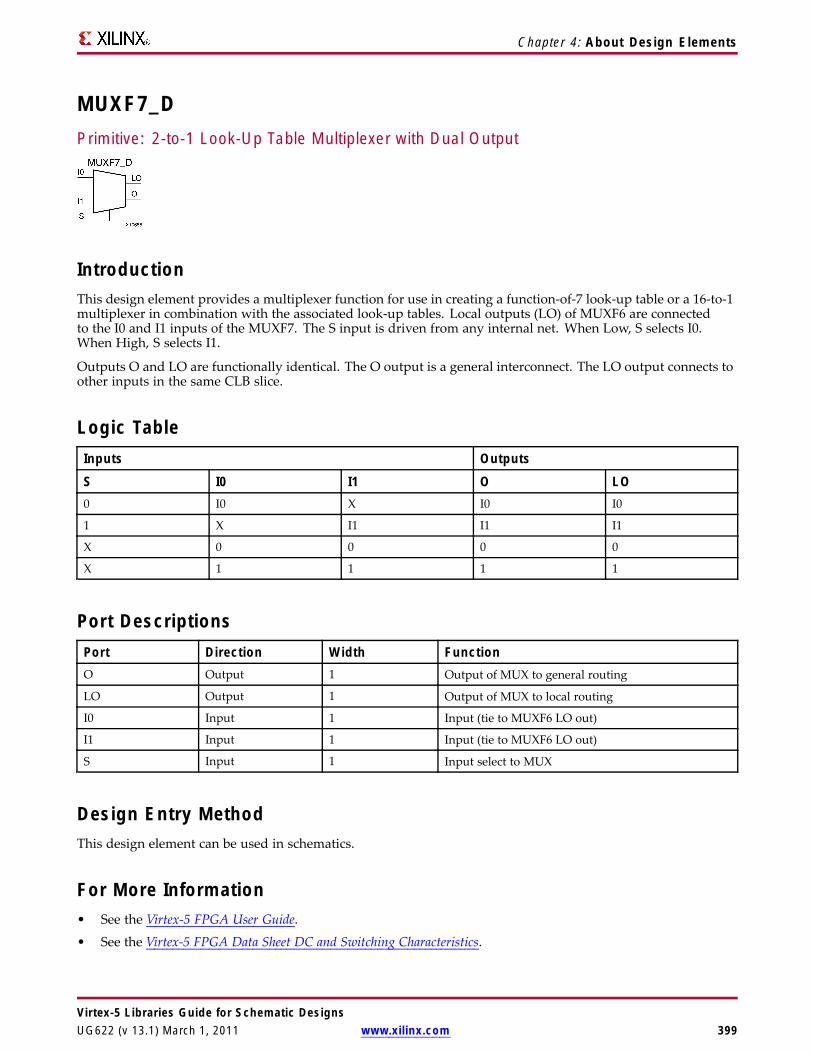
Chapter 4: About Design Elements
MUXF7_DPrimitive: 2-to-1 Look-Up Table Multiplexer with Dual Output
IntroductionThis design element provides a multiplexer function for use in creating a function-of-7 look-up table or a 16-to-1multiplexer in combination with the associated look-up tables. Local outputs (LO) of MUXF6 are connectedto the I0 and I1 inputs of the MUXF7. The S input is driven from any internal net. When Low, S selects I0.When High, S selects I1.
Outputs O and LO are functionally identical. The O output is a general interconnect. The LO output connects toother inputs in the same CLB slice.
Logic TableInputs Outputs
S I0 I1 O LO0 I0 X I0 I0
1 X I1 I1 I1
X 0 0 0 0
X 1 1 1 1
Port DescriptionsPort Direction Width FunctionO Output 1 Output of MUX to general routing
LO Output 1 Output of MUX to local routing
I0 Input 1 Input (tie to MUXF6 LO out)
I1 Input 1 Input (tie to MUXF6 LO out)
S Input 1 Input select to MUX
Design Entry MethodThis design element can be used in schematics.
For More Information• See the Virtex-5 FPGA User Guide.
• See the Virtex-5 FPGA Data Sheet DC and Switching Characteristics.
Virtex-5 Libraries Guide for Schematic DesignsUG622 (v 13.1) March 1, 2011 www.xilinx.com 399

Chapter 4: About Design Elements
MUXF7_LPrimitive: 2-to-1 look-up table Multiplexer with Local Output
IntroductionThis design element provides a multiplexer function for use in creating a function-of-7 look-up table or a 16-to-1multiplexer in combination with the associated look-up tables. Local outputs (LO) of MUXF6 are connectedto the I0 and I1 inputs of the MUXF7. The S input is driven from any internal net. When Low, S selects I0.When High, S selects I1.
The LO output connects to other inputs in the same CLB slice.
Logic TableInputs Output
S I0 I1 LO0 I0 X I0
1 X I1 I1
X 0 0 0
X 1 1 1
Port DescriptionsPort Direction Width FunctionLO Output 1 Output of MUX to local routing
I0 Input 1 Input
I1 Input 1 Input
S Input 1 Input select to MUX
Design Entry MethodThis design element can be used in schematics.
For More Information• See the Virtex-5 FPGA User Guide.
• See the Virtex-5 FPGA Data Sheet DC and Switching Characteristics.
Virtex-5 Libraries Guide for Schematic Designs400 www.xilinx.com UG622 (v 13.1) March 1, 2011
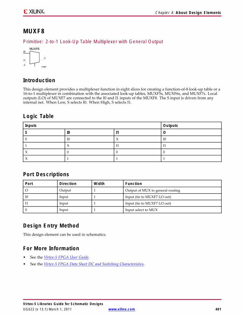
Chapter 4: About Design Elements
MUXF8Primitive: 2-to-1 Look-Up Table Multiplexer with General Output
IntroductionThis design element provides a multiplexer function in eight slices for creating a function-of-8 look-up table or a16-to-1 multiplexer in combination with the associated look-up tables, MUXF5s, MUXF6s, and MUXF7s. Localoutputs (LO) of MUXF7 are connected to the I0 and I1 inputs of the MUXF8. The S input is driven from anyinternal net. When Low, S selects I0. When High, S selects I1.
Logic TableInputs Outputs
S I0 I1 O0 I0 X I0
1 X I1 I1
X 0 0 0
X 1 1 1
Port DescriptionsPort Direction Width FunctionO Output 1 Output of MUX to general routing
I0 Input 1 Input (tie to MUXF7 LO out)
I1 Input 1 Input (tie to MUXF7 LO out)
S Input 1 Input select to MUX
Design Entry MethodThis design element can be used in schematics.
For More Information• See the Virtex-5 FPGA User Guide.
• See the Virtex-5 FPGA Data Sheet DC and Switching Characteristics.
Virtex-5 Libraries Guide for Schematic DesignsUG622 (v 13.1) March 1, 2011 www.xilinx.com 401
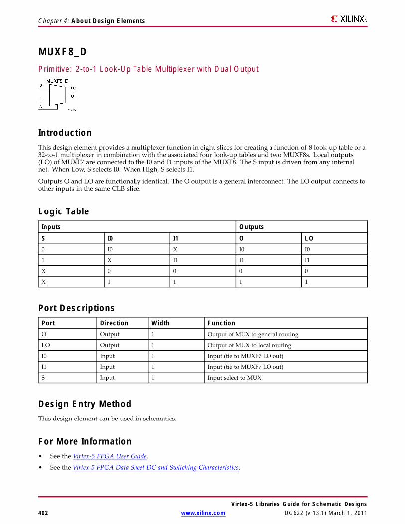
Chapter 4: About Design Elements
MUXF8_DPrimitive: 2-to-1 Look-Up Table Multiplexer with Dual Output
IntroductionThis design element provides a multiplexer function in eight slices for creating a function-of-8 look-up table or a32-to-1 multiplexer in combination with the associated four look-up tables and two MUXF8s. Local outputs(LO) of MUXF7 are connected to the I0 and I1 inputs of the MUXF8. The S input is driven from any internalnet. When Low, S selects I0. When High, S selects I1.
Outputs O and LO are functionally identical. The O output is a general interconnect. The LO output connects toother inputs in the same CLB slice.
Logic TableInputs Outputs
S I0 I1 O LO0 I0 X I0 I0
1 X I1 I1 I1
X 0 0 0 0
X 1 1 1 1
Port DescriptionsPort Direction Width FunctionO Output 1 Output of MUX to general routing
LO Output 1 Output of MUX to local routing
I0 Input 1 Input (tie to MUXF7 LO out)
I1 Input 1 Input (tie to MUXF7 LO out)
S Input 1 Input select to MUX
Design Entry MethodThis design element can be used in schematics.
For More Information• See the Virtex-5 FPGA User Guide.
• See the Virtex-5 FPGA Data Sheet DC and Switching Characteristics.
Virtex-5 Libraries Guide for Schematic Designs402 www.xilinx.com UG622 (v 13.1) March 1, 2011

Chapter 4: About Design Elements
MUXF8_LPrimitive: 2-to-1 Look-Up Table Multiplexer with Local Output
IntroductionThis design element provides a multiplexer function in eight slices for creating a function-of-8 look-up table or a32-to-1 multiplexer in combination with the associated four look-up tables and two MUXF8s. Local outputs(LO) of MUXF7 are connected to the I0 and I1 inputs of the MUXF8. The S input is driven from any internalnet. When Low, S selects I0. When High, S selects I1.
The LO output connects to other inputs in the same CLB slice.
Logic TableInputs Output
S I0 I1 LO0 I0 X I0
1 X I1 I1
X 0 0 0
X 1 1 1
Port DescriptionsPort Direction Width FunctionLO Output 1 Output of MUX to local routing
I0 Input 1 Input (tie to MUXF7 LO out)
I1 Input 1 Input (tie to MUXF7 LO out)
S Input 1 Input select to MUX
Design Entry MethodThis design element can be used in schematics.
For More Information• See the Virtex-5 FPGA User Guide.
• See the Virtex-5 FPGA Data Sheet DC and Switching Characteristics.
Virtex-5 Libraries Guide for Schematic DesignsUG622 (v 13.1) March 1, 2011 www.xilinx.com 403

Chapter 4: About Design Elements
NAND12Macro: 12- Input NAND Gate with Non-Inverted Inputs
IntroductionNAND gates of up to five inputs are available in any combination of inverting and non-inverting inputs. NANDgates of six to nine inputs, 12 inputs, and 16 inputs are available with only non-inverting inputs. To invert inputs,use external inverters. Because each input uses a CLB resource, replace gates with unused inputs with gateshaving the necessary number of inputs.
Design Entry MethodThis design element is only for use in schematics.
For More Information• See the Virtex-5 FPGA User Guide.
• See the Virtex-5 FPGA Data Sheet DC and Switching Characteristics.
Virtex-5 Libraries Guide for Schematic Designs404 www.xilinx.com UG622 (v 13.1) March 1, 2011
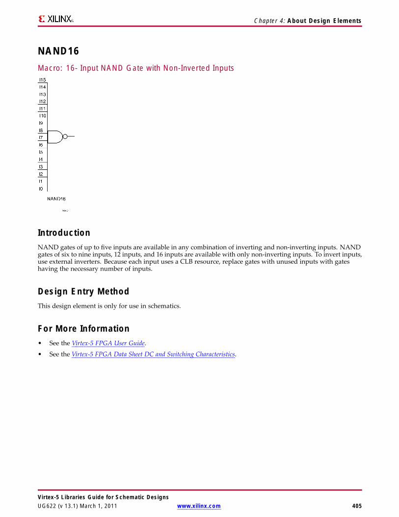
Chapter 4: About Design Elements
NAND16Macro: 16- Input NAND Gate with Non-Inverted Inputs
IntroductionNAND gates of up to five inputs are available in any combination of inverting and non-inverting inputs. NANDgates of six to nine inputs, 12 inputs, and 16 inputs are available with only non-inverting inputs. To invert inputs,use external inverters. Because each input uses a CLB resource, replace gates with unused inputs with gateshaving the necessary number of inputs.
Design Entry MethodThis design element is only for use in schematics.
For More Information• See the Virtex-5 FPGA User Guide.
• See the Virtex-5 FPGA Data Sheet DC and Switching Characteristics.
Virtex-5 Libraries Guide for Schematic DesignsUG622 (v 13.1) March 1, 2011 www.xilinx.com 405

Chapter 4: About Design Elements
NAND2Primitive: 2-Input NAND Gate with Non-Inverted Inputs
IntroductionNAND gates of up to five inputs are available in any combination of inverting and non-inverting inputs. NANDgates of six to nine inputs, 12 inputs, and 16 inputs are available with only non-inverting inputs. To invert inputs,use external inverters. Because each input uses a CLB resource, replace gates with unused inputs with gateshaving the necessary number of inputs.
Design Entry MethodThis design element is only for use in schematics.
For More Information• See the Virtex-5 FPGA User Guide.
• See the Virtex-5 FPGA Data Sheet DC and Switching Characteristics.
Virtex-5 Libraries Guide for Schematic Designs406 www.xilinx.com UG622 (v 13.1) March 1, 2011
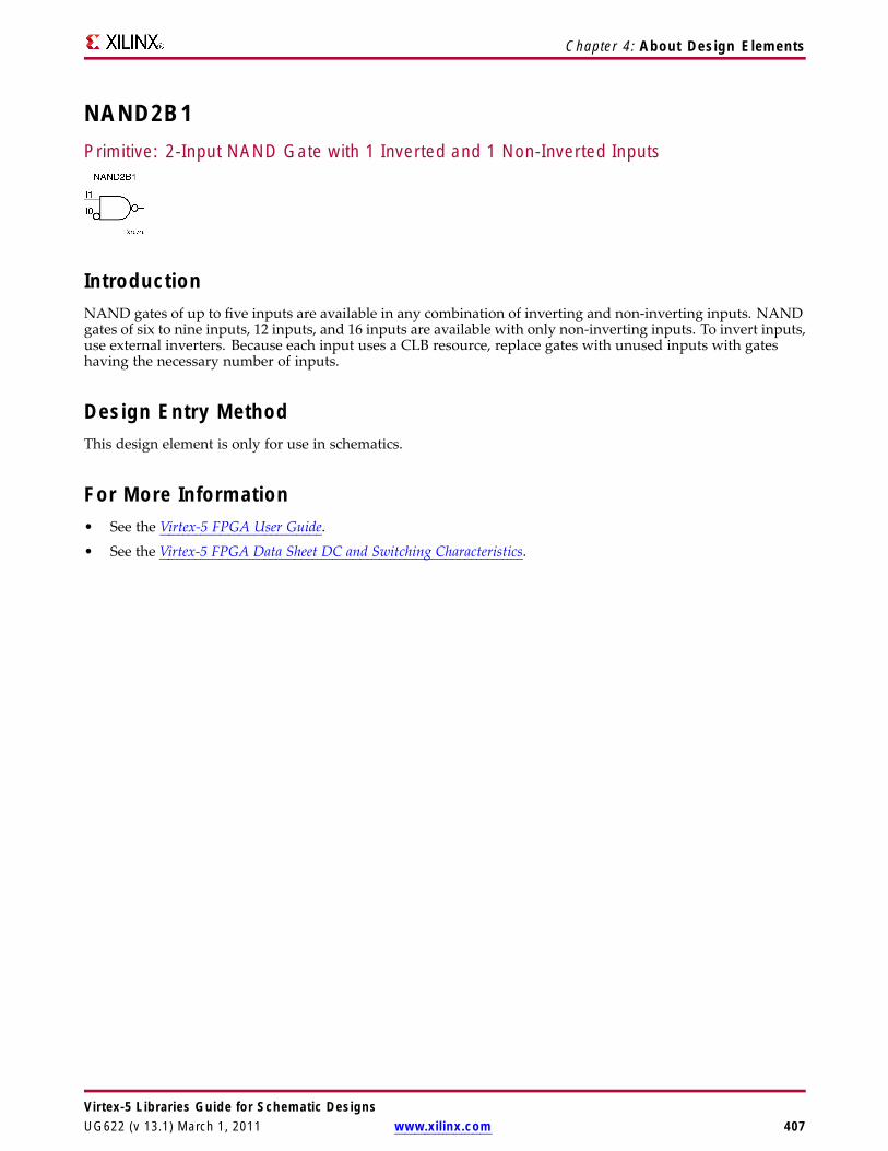
Chapter 4: About Design Elements
NAND2B1Primitive: 2-Input NAND Gate with 1 Inverted and 1 Non-Inverted Inputs
IntroductionNAND gates of up to five inputs are available in any combination of inverting and non-inverting inputs. NANDgates of six to nine inputs, 12 inputs, and 16 inputs are available with only non-inverting inputs. To invert inputs,use external inverters. Because each input uses a CLB resource, replace gates with unused inputs with gateshaving the necessary number of inputs.
Design Entry MethodThis design element is only for use in schematics.
For More Information• See the Virtex-5 FPGA User Guide.
• See the Virtex-5 FPGA Data Sheet DC and Switching Characteristics.
Virtex-5 Libraries Guide for Schematic DesignsUG622 (v 13.1) March 1, 2011 www.xilinx.com 407

Chapter 4: About Design Elements
NAND2B2Primitive: 2-Input NAND Gate with Inverted Inputs
IntroductionNAND gates of up to five inputs are available in any combination of inverting and non-inverting inputs. NANDgates of six to nine inputs, 12 inputs, and 16 inputs are available with only non-inverting inputs. To invert inputs,use external inverters. Because each input uses a CLB resource, replace gates with unused inputs with gateshaving the necessary number of inputs.
Design Entry MethodThis design element is only for use in schematics.
For More Information• See the Virtex-5 FPGA User Guide.
• See the Virtex-5 FPGA Data Sheet DC and Switching Characteristics.
Virtex-5 Libraries Guide for Schematic Designs408 www.xilinx.com UG622 (v 13.1) March 1, 2011

Chapter 4: About Design Elements
NAND3Primitive: 3-Input NAND Gate with Non-Inverted Inputs
IntroductionNAND gates of up to five inputs are available in any combination of inverting and non-inverting inputs. NANDgates of six to nine inputs, 12 inputs, and 16 inputs are available with only non-inverting inputs. To invert inputs,use external inverters. Because each input uses a CLB resource, replace gates with unused inputs with gateshaving the necessary number of inputs.
Design Entry MethodThis design element is only for use in schematics.
For More Information• See the Virtex-5 FPGA User Guide.
• See the Virtex-5 FPGA Data Sheet DC and Switching Characteristics.
Virtex-5 Libraries Guide for Schematic DesignsUG622 (v 13.1) March 1, 2011 www.xilinx.com 409
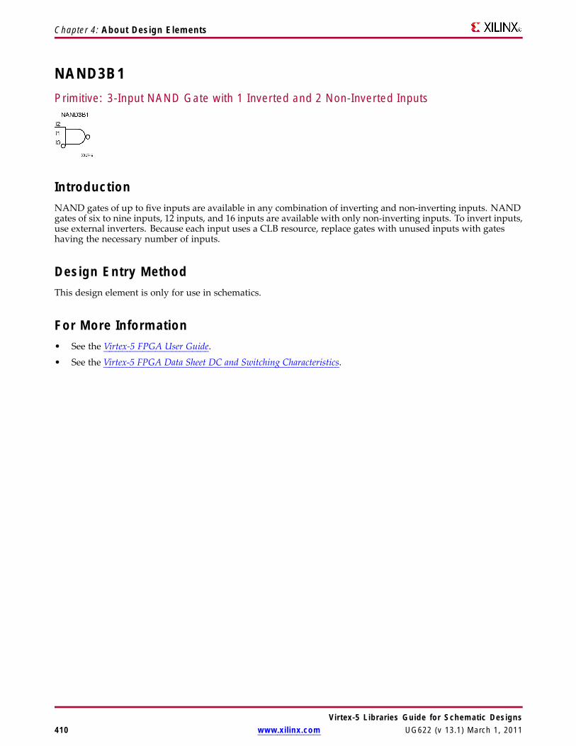
Chapter 4: About Design Elements
NAND3B1Primitive: 3-Input NAND Gate with 1 Inverted and 2 Non-Inverted Inputs
IntroductionNAND gates of up to five inputs are available in any combination of inverting and non-inverting inputs. NANDgates of six to nine inputs, 12 inputs, and 16 inputs are available with only non-inverting inputs. To invert inputs,use external inverters. Because each input uses a CLB resource, replace gates with unused inputs with gateshaving the necessary number of inputs.
Design Entry MethodThis design element is only for use in schematics.
For More Information• See the Virtex-5 FPGA User Guide.
• See the Virtex-5 FPGA Data Sheet DC and Switching Characteristics.
Virtex-5 Libraries Guide for Schematic Designs410 www.xilinx.com UG622 (v 13.1) March 1, 2011

Chapter 4: About Design Elements
NAND3B2Primitive: 3-Input NAND Gate with 2 Inverted and 1 Non-Inverted Inputs
IntroductionNAND gates of up to five inputs are available in any combination of inverting and non-inverting inputs. NANDgates of six to nine inputs, 12 inputs, and 16 inputs are available with only non-inverting inputs. To invert inputs,use external inverters. Because each input uses a CLB resource, replace gates with unused inputs with gateshaving the necessary number of inputs.
Design Entry MethodThis design element is only for use in schematics.
For More Information• See the Virtex-5 FPGA User Guide.
• See the Virtex-5 FPGA Data Sheet DC and Switching Characteristics.
Virtex-5 Libraries Guide for Schematic DesignsUG622 (v 13.1) March 1, 2011 www.xilinx.com 411

Chapter 4: About Design Elements
NAND3B3Primitive: 3-Input NAND Gate with Inverted Inputs
IntroductionNAND gates of up to five inputs are available in any combination of inverting and non-inverting inputs. NANDgates of six to nine inputs, 12 inputs, and 16 inputs are available with only non-inverting inputs. To invert inputs,use external inverters. Because each input uses a CLB resource, replace gates with unused inputs with gateshaving the necessary number of inputs.
Design Entry MethodThis design element is only for use in schematics.
For More Information• See the Virtex-5 FPGA User Guide.
• See the Virtex-5 FPGA Data Sheet DC and Switching Characteristics.
Virtex-5 Libraries Guide for Schematic Designs412 www.xilinx.com UG622 (v 13.1) March 1, 2011

Chapter 4: About Design Elements
NAND4Primitive: 4-Input NAND Gate with Non-Inverted Inputs
IntroductionNAND gates of up to five inputs are available in any combination of inverting and non-inverting inputs. NANDgates of six to nine inputs, 12 inputs, and 16 inputs are available with only non-inverting inputs. To invert inputs,use external inverters. Because each input uses a CLB resource, replace gates with unused inputs with gateshaving the necessary number of inputs.
Design Entry MethodThis design element is only for use in schematics.
For More Information• See the Virtex-5 FPGA User Guide.
• See the Virtex-5 FPGA Data Sheet DC and Switching Characteristics.
Virtex-5 Libraries Guide for Schematic DesignsUG622 (v 13.1) March 1, 2011 www.xilinx.com 413

Chapter 4: About Design Elements
NAND4B1Primitive: 4-Input NAND Gate with 1 Inverted and 3 Non-Inverted Inputs
IntroductionNAND gates of up to five inputs are available in any combination of inverting and non-inverting inputs. NANDgates of six to nine inputs, 12 inputs, and 16 inputs are available with only non-inverting inputs. To invert inputs,use external inverters. Because each input uses a CLB resource, replace gates with unused inputs with gateshaving the necessary number of inputs.
Design Entry MethodThis design element is only for use in schematics.
For More Information• See the Virtex-5 FPGA User Guide.
• See the Virtex-5 FPGA Data Sheet DC and Switching Characteristics.
Virtex-5 Libraries Guide for Schematic Designs414 www.xilinx.com UG622 (v 13.1) March 1, 2011

Chapter 4: About Design Elements
NAND4B2Primitive: 4-Input NAND Gate with 2 Inverted and 2 Non-Inverted Inputs
IntroductionNAND gates of up to five inputs are available in any combination of inverting and non-inverting inputs. NANDgates of six to nine inputs, 12 inputs, and 16 inputs are available with only non-inverting inputs. To invert inputs,use external inverters. Because each input uses a CLB resource, replace gates with unused inputs with gateshaving the necessary number of inputs.
Design Entry MethodThis design element is only for use in schematics.
For More Information• See the Virtex-5 FPGA User Guide.
• See the Virtex-5 FPGA Data Sheet DC and Switching Characteristics.
Virtex-5 Libraries Guide for Schematic DesignsUG622 (v 13.1) March 1, 2011 www.xilinx.com 415

Chapter 4: About Design Elements
NAND4B3Primitive: 4-Input NAND Gate with 3 Inverted and 1 Non-Inverted Inputs
IntroductionNAND gates of up to five inputs are available in any combination of inverting and non-inverting inputs. NANDgates of six to nine inputs, 12 inputs, and 16 inputs are available with only non-inverting inputs. To invert inputs,use external inverters. Because each input uses a CLB resource, replace gates with unused inputs with gateshaving the necessary number of inputs.
Design Entry MethodThis design element is only for use in schematics.
For More Information• See the Virtex-5 FPGA User Guide.
• See the Virtex-5 FPGA Data Sheet DC and Switching Characteristics.
Virtex-5 Libraries Guide for Schematic Designs416 www.xilinx.com UG622 (v 13.1) March 1, 2011
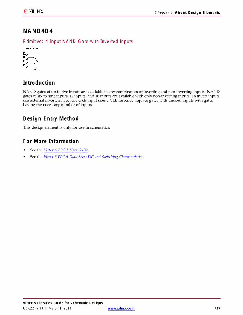
Chapter 4: About Design Elements
NAND4B4Primitive: 4-Input NAND Gate with Inverted Inputs
IntroductionNAND gates of up to five inputs are available in any combination of inverting and non-inverting inputs. NANDgates of six to nine inputs, 12 inputs, and 16 inputs are available with only non-inverting inputs. To invert inputs,use external inverters. Because each input uses a CLB resource, replace gates with unused inputs with gateshaving the necessary number of inputs.
Design Entry MethodThis design element is only for use in schematics.
For More Information• See the Virtex-5 FPGA User Guide.
• See the Virtex-5 FPGA Data Sheet DC and Switching Characteristics.
Virtex-5 Libraries Guide for Schematic DesignsUG622 (v 13.1) March 1, 2011 www.xilinx.com 417

Chapter 4: About Design Elements
NAND5Primitive: 5-Input NAND Gate with Non-Inverted Inputs
IntroductionNAND gates of up to five inputs are available in any combination of inverting and non-inverting inputs. NANDgates of six to nine inputs, 12 inputs, and 16 inputs are available with only non-inverting inputs. To invert inputs,use external inverters. Because each input uses a CLB resource, replace gates with unused inputs with gateshaving the necessary number of inputs.
Design Entry MethodThis design element is only for use in schematics.
For More Information• See the Virtex-5 FPGA User Guide.
• See the Virtex-5 FPGA Data Sheet DC and Switching Characteristics.
Virtex-5 Libraries Guide for Schematic Designs418 www.xilinx.com UG622 (v 13.1) March 1, 2011
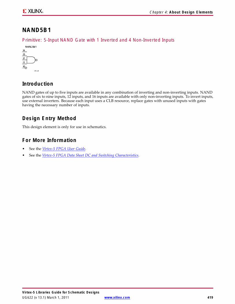
Chapter 4: About Design Elements
NAND5B1Primitive: 5-Input NAND Gate with 1 Inverted and 4 Non-Inverted Inputs
IntroductionNAND gates of up to five inputs are available in any combination of inverting and non-inverting inputs. NANDgates of six to nine inputs, 12 inputs, and 16 inputs are available with only non-inverting inputs. To invert inputs,use external inverters. Because each input uses a CLB resource, replace gates with unused inputs with gateshaving the necessary number of inputs.
Design Entry MethodThis design element is only for use in schematics.
For More Information• See the Virtex-5 FPGA User Guide.
• See the Virtex-5 FPGA Data Sheet DC and Switching Characteristics.
Virtex-5 Libraries Guide for Schematic DesignsUG622 (v 13.1) March 1, 2011 www.xilinx.com 419

Chapter 4: About Design Elements
NAND5B2Primitive: 5-Input NAND Gate with 2 Inverted and 3 Non-Inverted Inputs
IntroductionNAND gates of up to five inputs are available in any combination of inverting and non-inverting inputs. NANDgates of six to nine inputs, 12 inputs, and 16 inputs are available with only non-inverting inputs. To invert inputs,use external inverters. Because each input uses a CLB resource, replace gates with unused inputs with gateshaving the necessary number of inputs.
Design Entry MethodThis design element is only for use in schematics.
For More Information• See the Virtex-5 FPGA User Guide.
• See the Virtex-5 FPGA Data Sheet DC and Switching Characteristics.
Virtex-5 Libraries Guide for Schematic Designs420 www.xilinx.com UG622 (v 13.1) March 1, 2011

Chapter 4: About Design Elements
NAND5B3Primitive: 5-Input NAND Gate with 3 Inverted and 2 Non-Inverted Inputs
IntroductionNAND gates of up to five inputs are available in any combination of inverting and non-inverting inputs. NANDgates of six to nine inputs, 12 inputs, and 16 inputs are available with only non-inverting inputs. To invert inputs,use external inverters. Because each input uses a CLB resource, replace gates with unused inputs with gateshaving the necessary number of inputs.
Design Entry MethodThis design element is only for use in schematics.
For More Information• See the Virtex-5 FPGA User Guide.
• See the Virtex-5 FPGA Data Sheet DC and Switching Characteristics.
Virtex-5 Libraries Guide for Schematic DesignsUG622 (v 13.1) March 1, 2011 www.xilinx.com 421
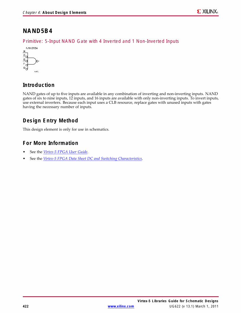
Chapter 4: About Design Elements
NAND5B4Primitive: 5-Input NAND Gate with 4 Inverted and 1 Non-Inverted Inputs
IntroductionNAND gates of up to five inputs are available in any combination of inverting and non-inverting inputs. NANDgates of six to nine inputs, 12 inputs, and 16 inputs are available with only non-inverting inputs. To invert inputs,use external inverters. Because each input uses a CLB resource, replace gates with unused inputs with gateshaving the necessary number of inputs.
Design Entry MethodThis design element is only for use in schematics.
For More Information• See the Virtex-5 FPGA User Guide.
• See the Virtex-5 FPGA Data Sheet DC and Switching Characteristics.
Virtex-5 Libraries Guide for Schematic Designs422 www.xilinx.com UG622 (v 13.1) March 1, 2011

Chapter 4: About Design Elements
NAND5B5Primitive: 5-Input NAND Gate with Inverted Inputs
IntroductionNAND gates of up to five inputs are available in any combination of inverting and non-inverting inputs. NANDgates of six to nine inputs, 12 inputs, and 16 inputs are available with only non-inverting inputs. To invert inputs,use external inverters. Because each input uses a CLB resource, replace gates with unused inputs with gateshaving the necessary number of inputs.
Design Entry MethodThis design element is only for use in schematics.
For More Information• See the Virtex-5 FPGA User Guide.
• See the Virtex-5 FPGA Data Sheet DC and Switching Characteristics.
Virtex-5 Libraries Guide for Schematic DesignsUG622 (v 13.1) March 1, 2011 www.xilinx.com 423

Chapter 4: About Design Elements
NAND6Macro: 6-Input NAND Gate with Non-Inverted Inputs
IntroductionNAND gates of up to five inputs are available in any combination of inverting and non-inverting inputs. NANDgates of six to nine inputs, 12 inputs, and 16 inputs are available with only non-inverting inputs. To invert inputs,use external inverters. Because each input uses a CLB resource, replace gates with unused inputs with gateshaving the necessary number of inputs.
Design Entry MethodThis design element is only for use in schematics.
For More Information• See the Virtex-5 FPGA User Guide.
• See the Virtex-5 FPGA Data Sheet DC and Switching Characteristics.
Virtex-5 Libraries Guide for Schematic Designs424 www.xilinx.com UG622 (v 13.1) March 1, 2011

Chapter 4: About Design Elements
NAND7Macro: 7-Input NAND Gate with Non-Inverted Inputs
IntroductionNAND gates of up to five inputs are available in any combination of inverting and non-inverting inputs. NANDgates of six to nine inputs, 12 inputs, and 16 inputs are available with only non-inverting inputs. To invert inputs,use external inverters. Because each input uses a CLB resource, replace gates with unused inputs with gateshaving the necessary number of inputs.
Design Entry MethodThis design element is only for use in schematics.
For More Information• See the Virtex-5 FPGA User Guide.
• See the Virtex-5 FPGA Data Sheet DC and Switching Characteristics.
Virtex-5 Libraries Guide for Schematic DesignsUG622 (v 13.1) March 1, 2011 www.xilinx.com 425
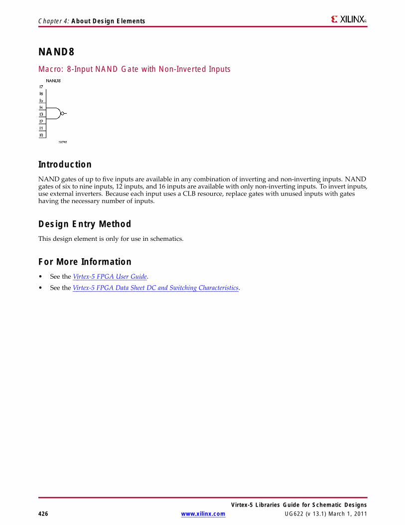
Chapter 4: About Design Elements
NAND8Macro: 8-Input NAND Gate with Non-Inverted Inputs
IntroductionNAND gates of up to five inputs are available in any combination of inverting and non-inverting inputs. NANDgates of six to nine inputs, 12 inputs, and 16 inputs are available with only non-inverting inputs. To invert inputs,use external inverters. Because each input uses a CLB resource, replace gates with unused inputs with gateshaving the necessary number of inputs.
Design Entry MethodThis design element is only for use in schematics.
For More Information• See the Virtex-5 FPGA User Guide.
• See the Virtex-5 FPGA Data Sheet DC and Switching Characteristics.
Virtex-5 Libraries Guide for Schematic Designs426 www.xilinx.com UG622 (v 13.1) March 1, 2011
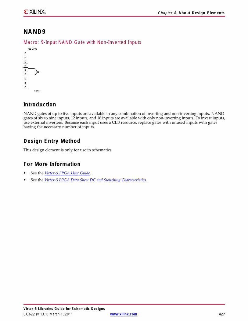
Chapter 4: About Design Elements
NAND9Macro: 9-Input NAND Gate with Non-Inverted Inputs
IntroductionNAND gates of up to five inputs are available in any combination of inverting and non-inverting inputs. NANDgates of six to nine inputs, 12 inputs, and 16 inputs are available with only non-inverting inputs. To invert inputs,use external inverters. Because each input uses a CLB resource, replace gates with unused inputs with gateshaving the necessary number of inputs.
Design Entry MethodThis design element is only for use in schematics.
For More Information• See the Virtex-5 FPGA User Guide.
• See the Virtex-5 FPGA Data Sheet DC and Switching Characteristics.
Virtex-5 Libraries Guide for Schematic DesignsUG622 (v 13.1) March 1, 2011 www.xilinx.com 427

Chapter 4: About Design Elements
NOR12Macro: 12-Input NOR Gate with Non-Inverted Inputs
IntroductionNOR gates of up to five inputs are available in any combination of inverting and non-inverting inputs. NORgates of six to nine inputs, 12 inputs, and 16 inputs are available only with non-inverting inputs. To invert someor all inputs, use external inverters. Because each input uses a CLB resource, replace gates with unused inputswith gates having the necessary number of inputs.
Design Entry MethodThis design element is only for use in schematics.
For More Information• See the Virtex-5 FPGA User Guide.
• See the Virtex-5 FPGA Data Sheet DC and Switching Characteristics.
Virtex-5 Libraries Guide for Schematic Designs428 www.xilinx.com UG622 (v 13.1) March 1, 2011
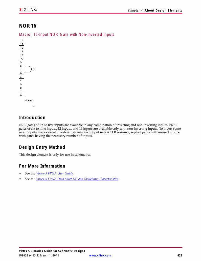
Chapter 4: About Design Elements
NOR16Macro: 16-Input NOR Gate with Non-Inverted Inputs
IntroductionNOR gates of up to five inputs are available in any combination of inverting and non-inverting inputs. NORgates of six to nine inputs, 12 inputs, and 16 inputs are available only with non-inverting inputs. To invert someor all inputs, use external inverters. Because each input uses a CLB resource, replace gates with unused inputswith gates having the necessary number of inputs.
Design Entry MethodThis design element is only for use in schematics.
For More Information• See the Virtex-5 FPGA User Guide.
• See the Virtex-5 FPGA Data Sheet DC and Switching Characteristics.
Virtex-5 Libraries Guide for Schematic DesignsUG622 (v 13.1) March 1, 2011 www.xilinx.com 429

Chapter 4: About Design Elements
NOR2Primitive: 2-Input NOR Gate with Non-Inverted Inputs
IntroductionNOR gates of up to five inputs are available in any combination of inverting and non-inverting inputs. NORgates of six to nine inputs, 12 inputs, and 16 inputs are available only with non-inverting inputs. To invert someor all inputs, use external inverters. Because each input uses a CLB resource, replace gates with unused inputswith gates having the necessary number of inputs.
Design Entry MethodThis design element is only for use in schematics.
For More Information• See the Virtex-5 FPGA User Guide.
• See the Virtex-5 FPGA Data Sheet DC and Switching Characteristics.
Virtex-5 Libraries Guide for Schematic Designs430 www.xilinx.com UG622 (v 13.1) March 1, 2011

Chapter 4: About Design Elements
NOR2B1Primitive: 2-Input NOR Gate with 1 Inverted and 1 Non-Inverted Inputs
IntroductionNOR gates of up to five inputs are available in any combination of inverting and non-inverting inputs. NORgates of six to nine inputs, 12 inputs, and 16 inputs are available only with non-inverting inputs. To invert someor all inputs, use external inverters. Because each input uses a CLB resource, replace gates with unused inputswith gates having the necessary number of inputs.
Design Entry MethodThis design element is only for use in schematics.
For More Information• See the Virtex-5 FPGA User Guide.
• See the Virtex-5 FPGA Data Sheet DC and Switching Characteristics.
Virtex-5 Libraries Guide for Schematic DesignsUG622 (v 13.1) March 1, 2011 www.xilinx.com 431
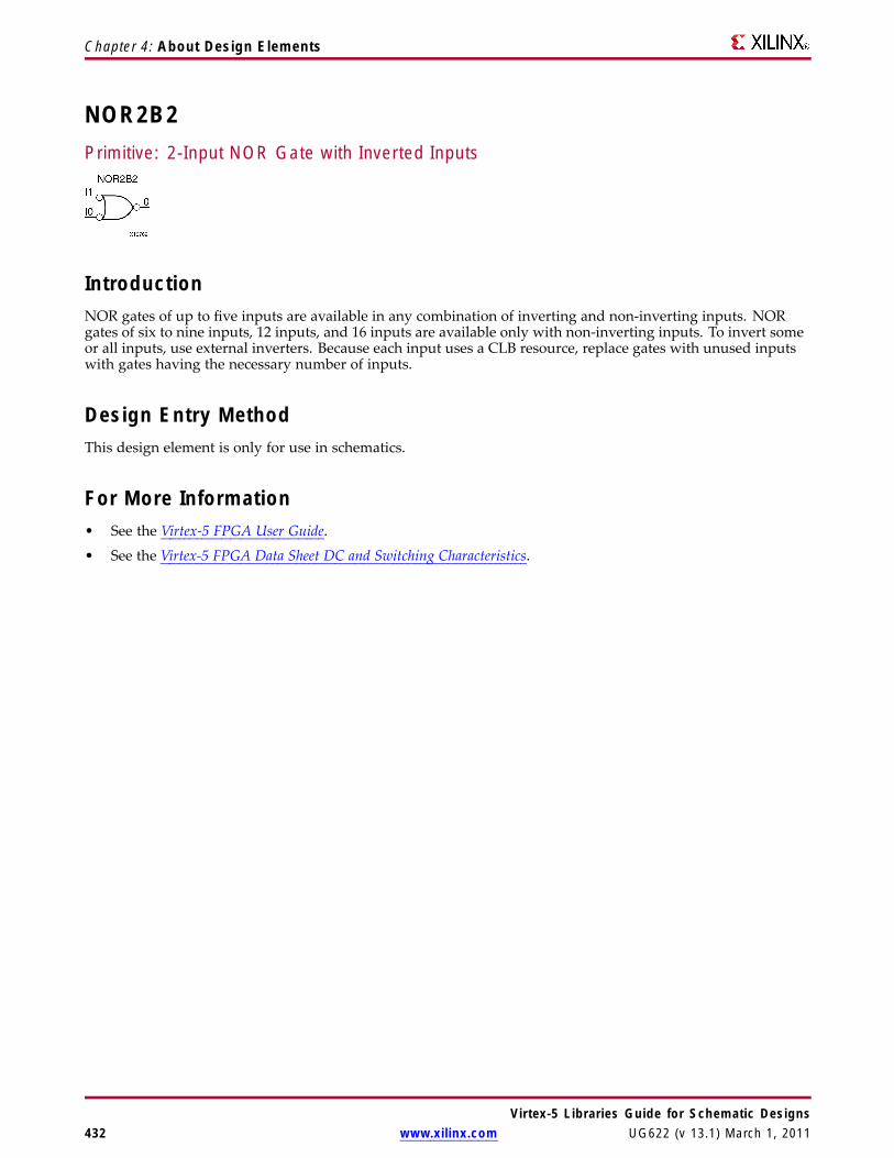
Chapter 4: About Design Elements
NOR2B2Primitive: 2-Input NOR Gate with Inverted Inputs
IntroductionNOR gates of up to five inputs are available in any combination of inverting and non-inverting inputs. NORgates of six to nine inputs, 12 inputs, and 16 inputs are available only with non-inverting inputs. To invert someor all inputs, use external inverters. Because each input uses a CLB resource, replace gates with unused inputswith gates having the necessary number of inputs.
Design Entry MethodThis design element is only for use in schematics.
For More Information• See the Virtex-5 FPGA User Guide.
• See the Virtex-5 FPGA Data Sheet DC and Switching Characteristics.
Virtex-5 Libraries Guide for Schematic Designs432 www.xilinx.com UG622 (v 13.1) March 1, 2011
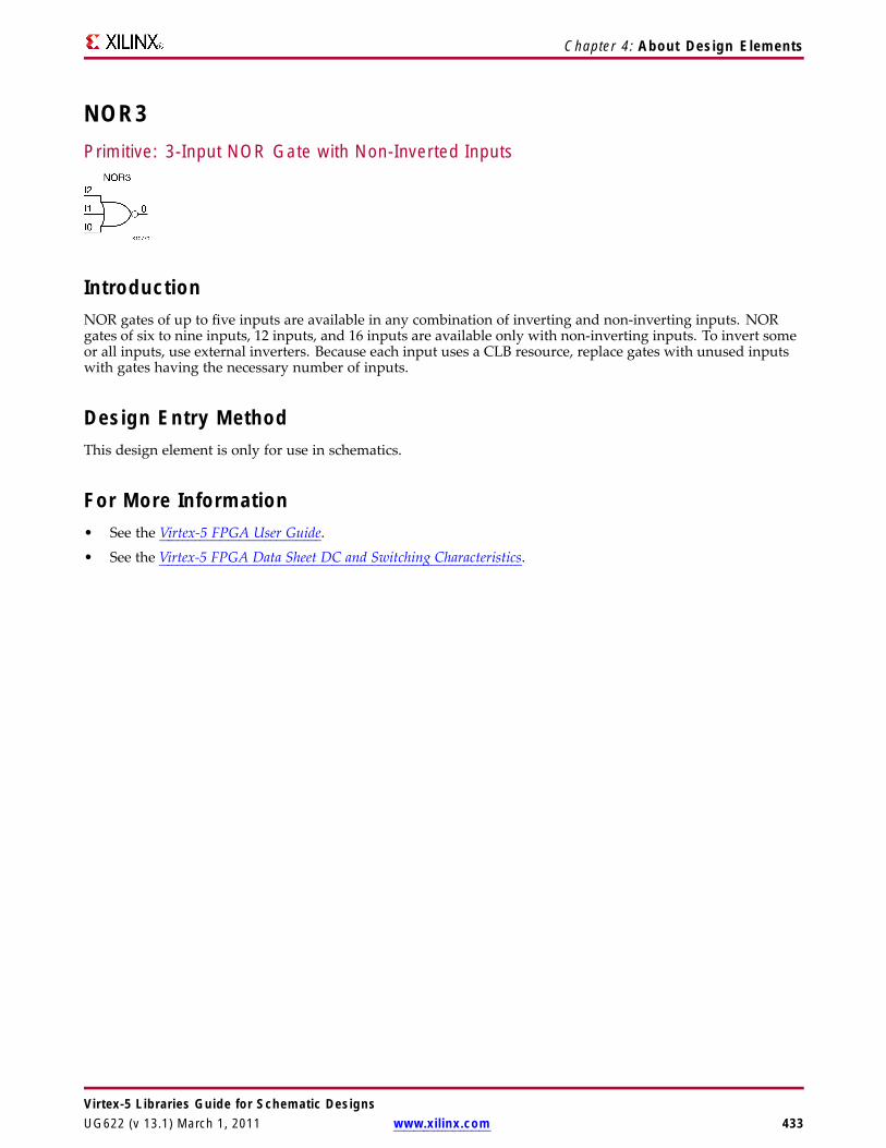
Chapter 4: About Design Elements
NOR3Primitive: 3-Input NOR Gate with Non-Inverted Inputs
IntroductionNOR gates of up to five inputs are available in any combination of inverting and non-inverting inputs. NORgates of six to nine inputs, 12 inputs, and 16 inputs are available only with non-inverting inputs. To invert someor all inputs, use external inverters. Because each input uses a CLB resource, replace gates with unused inputswith gates having the necessary number of inputs.
Design Entry MethodThis design element is only for use in schematics.
For More Information• See the Virtex-5 FPGA User Guide.
• See the Virtex-5 FPGA Data Sheet DC and Switching Characteristics.
Virtex-5 Libraries Guide for Schematic DesignsUG622 (v 13.1) March 1, 2011 www.xilinx.com 433

Chapter 4: About Design Elements
NOR3B1Primitive: 3-Input NOR Gate with 1 Inverted and 2 Non-Inverted Inputs
IntroductionNOR gates of up to five inputs are available in any combination of inverting and non-inverting inputs. NORgates of six to nine inputs, 12 inputs, and 16 inputs are available only with non-inverting inputs. To invert someor all inputs, use external inverters. Because each input uses a CLB resource, replace gates with unused inputswith gates having the necessary number of inputs.
Design Entry MethodThis design element is only for use in schematics.
For More Information• See the Virtex-5 FPGA User Guide.
• See the Virtex-5 FPGA Data Sheet DC and Switching Characteristics.
Virtex-5 Libraries Guide for Schematic Designs434 www.xilinx.com UG622 (v 13.1) March 1, 2011

Chapter 4: About Design Elements
NOR3B2Primitive: 3-Input NOR Gate with 2 Inverted and 1 Non-Inverted Inputs
IntroductionNOR gates of up to five inputs are available in any combination of inverting and non-inverting inputs. NORgates of six to nine inputs, 12 inputs, and 16 inputs are available only with non-inverting inputs. To invert someor all inputs, use external inverters. Because each input uses a CLB resource, replace gates with unused inputswith gates having the necessary number of inputs.
Design Entry MethodThis design element is only for use in schematics.
For More Information• See the Virtex-5 FPGA User Guide.
• See the Virtex-5 FPGA Data Sheet DC and Switching Characteristics.
Virtex-5 Libraries Guide for Schematic DesignsUG622 (v 13.1) March 1, 2011 www.xilinx.com 435

Chapter 4: About Design Elements
NOR3B3Primitive: 3-Input NOR Gate with Inverted Inputs
IntroductionNOR gates of up to five inputs are available in any combination of inverting and non-inverting inputs. NORgates of six to nine inputs, 12 inputs, and 16 inputs are available only with non-inverting inputs. To invert someor all inputs, use external inverters. Because each input uses a CLB resource, replace gates with unused inputswith gates having the necessary number of inputs.
Design Entry MethodThis design element is only for use in schematics.
For More Information• See the Virtex-5 FPGA User Guide.
• See the Virtex-5 FPGA Data Sheet DC and Switching Characteristics.
Virtex-5 Libraries Guide for Schematic Designs436 www.xilinx.com UG622 (v 13.1) March 1, 2011

Chapter 4: About Design Elements
NOR4Primitive: 4-Input NOR Gate with Non-Inverted Inputs
IntroductionNOR gates of up to five inputs are available in any combination of inverting and non-inverting inputs. NORgates of six to nine inputs, 12 inputs, and 16 inputs are available only with non-inverting inputs. To invert someor all inputs, use external inverters. Because each input uses a CLB resource, replace gates with unused inputswith gates having the necessary number of inputs.
Design Entry MethodThis design element is only for use in schematics.
For More Information• See the Virtex-5 FPGA User Guide.
• See the Virtex-5 FPGA Data Sheet DC and Switching Characteristics.
Virtex-5 Libraries Guide for Schematic DesignsUG622 (v 13.1) March 1, 2011 www.xilinx.com 437
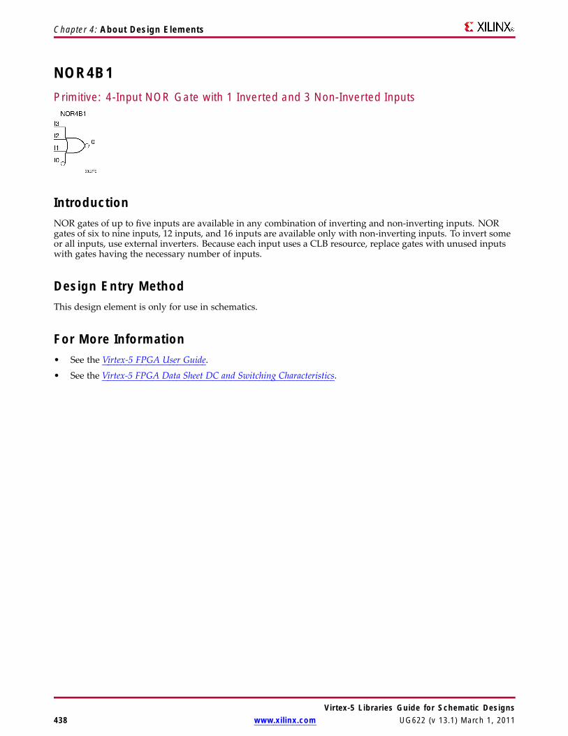
Chapter 4: About Design Elements
NOR4B1Primitive: 4-Input NOR Gate with 1 Inverted and 3 Non-Inverted Inputs
IntroductionNOR gates of up to five inputs are available in any combination of inverting and non-inverting inputs. NORgates of six to nine inputs, 12 inputs, and 16 inputs are available only with non-inverting inputs. To invert someor all inputs, use external inverters. Because each input uses a CLB resource, replace gates with unused inputswith gates having the necessary number of inputs.
Design Entry MethodThis design element is only for use in schematics.
For More Information• See the Virtex-5 FPGA User Guide.
• See the Virtex-5 FPGA Data Sheet DC and Switching Characteristics.
Virtex-5 Libraries Guide for Schematic Designs438 www.xilinx.com UG622 (v 13.1) March 1, 2011

Chapter 4: About Design Elements
NOR4B2Primitive: 4-Input NOR Gate with 2 Inverted and 2 Non-Inverted Inputs
IntroductionNOR gates of up to five inputs are available in any combination of inverting and non-inverting inputs. NORgates of six to nine inputs, 12 inputs, and 16 inputs are available only with non-inverting inputs. To invert someor all inputs, use external inverters. Because each input uses a CLB resource, replace gates with unused inputswith gates having the necessary number of inputs.
Design Entry MethodThis design element is only for use in schematics.
For More Information• See the Virtex-5 FPGA User Guide.
• See the Virtex-5 FPGA Data Sheet DC and Switching Characteristics.
Virtex-5 Libraries Guide for Schematic DesignsUG622 (v 13.1) March 1, 2011 www.xilinx.com 439

Chapter 4: About Design Elements
NOR4B3Primitive: 4-Input NOR Gate with 3 Inverted and 1 Non-Inverted Inputs
IntroductionNOR gates of up to five inputs are available in any combination of inverting and non-inverting inputs. NORgates of six to nine inputs, 12 inputs, and 16 inputs are available only with non-inverting inputs. To invert someor all inputs, use external inverters. Because each input uses a CLB resource, replace gates with unused inputswith gates having the necessary number of inputs.
Design Entry MethodThis design element is only for use in schematics.
For More Information• See the Virtex-5 FPGA User Guide.
• See the Virtex-5 FPGA Data Sheet DC and Switching Characteristics.
Virtex-5 Libraries Guide for Schematic Designs440 www.xilinx.com UG622 (v 13.1) March 1, 2011
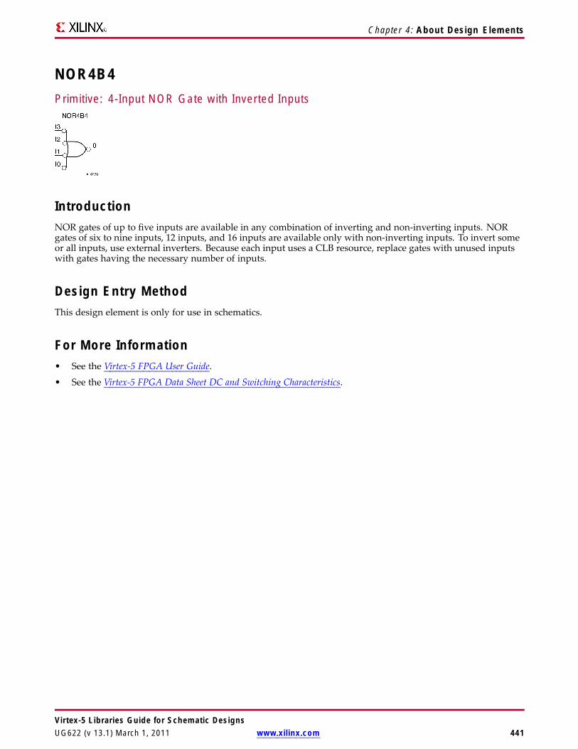
Chapter 4: About Design Elements
NOR4B4Primitive: 4-Input NOR Gate with Inverted Inputs
IntroductionNOR gates of up to five inputs are available in any combination of inverting and non-inverting inputs. NORgates of six to nine inputs, 12 inputs, and 16 inputs are available only with non-inverting inputs. To invert someor all inputs, use external inverters. Because each input uses a CLB resource, replace gates with unused inputswith gates having the necessary number of inputs.
Design Entry MethodThis design element is only for use in schematics.
For More Information• See the Virtex-5 FPGA User Guide.
• See the Virtex-5 FPGA Data Sheet DC and Switching Characteristics.
Virtex-5 Libraries Guide for Schematic DesignsUG622 (v 13.1) March 1, 2011 www.xilinx.com 441
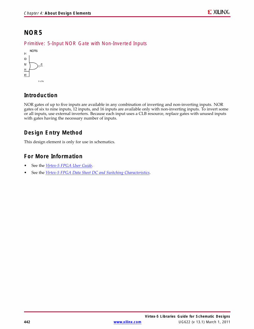
Chapter 4: About Design Elements
NOR5Primitive: 5-Input NOR Gate with Non-Inverted Inputs
IntroductionNOR gates of up to five inputs are available in any combination of inverting and non-inverting inputs. NORgates of six to nine inputs, 12 inputs, and 16 inputs are available only with non-inverting inputs. To invert someor all inputs, use external inverters. Because each input uses a CLB resource, replace gates with unused inputswith gates having the necessary number of inputs.
Design Entry MethodThis design element is only for use in schematics.
For More Information• See the Virtex-5 FPGA User Guide.
• See the Virtex-5 FPGA Data Sheet DC and Switching Characteristics.
Virtex-5 Libraries Guide for Schematic Designs442 www.xilinx.com UG622 (v 13.1) March 1, 2011

Chapter 4: About Design Elements
NOR5B1Primitive: 5-Input NOR Gate with 1 Inverted and 4 Non-Inverted Inputs
IntroductionNOR gates of up to five inputs are available in any combination of inverting and non-inverting inputs. NORgates of six to nine inputs, 12 inputs, and 16 inputs are available only with non-inverting inputs. To invert someor all inputs, use external inverters. Because each input uses a CLB resource, replace gates with unused inputswith gates having the necessary number of inputs.
Design Entry MethodThis design element is only for use in schematics.
For More Information• See the Virtex-5 FPGA User Guide.
• See the Virtex-5 FPGA Data Sheet DC and Switching Characteristics.
Virtex-5 Libraries Guide for Schematic DesignsUG622 (v 13.1) March 1, 2011 www.xilinx.com 443
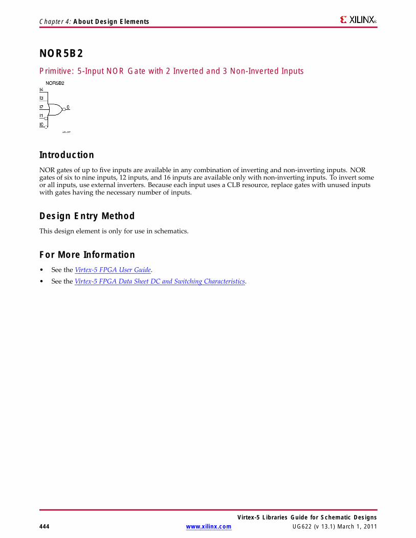
Chapter 4: About Design Elements
NOR5B2Primitive: 5-Input NOR Gate with 2 Inverted and 3 Non-Inverted Inputs
IntroductionNOR gates of up to five inputs are available in any combination of inverting and non-inverting inputs. NORgates of six to nine inputs, 12 inputs, and 16 inputs are available only with non-inverting inputs. To invert someor all inputs, use external inverters. Because each input uses a CLB resource, replace gates with unused inputswith gates having the necessary number of inputs.
Design Entry MethodThis design element is only for use in schematics.
For More Information• See the Virtex-5 FPGA User Guide.
• See the Virtex-5 FPGA Data Sheet DC and Switching Characteristics.
Virtex-5 Libraries Guide for Schematic Designs444 www.xilinx.com UG622 (v 13.1) March 1, 2011

Chapter 4: About Design Elements
NOR5B3Primitive: 5-Input NOR Gate with 3 Inverted and 2 Non-Inverted Inputs
IntroductionNOR gates of up to five inputs are available in any combination of inverting and non-inverting inputs. NORgates of six to nine inputs, 12 inputs, and 16 inputs are available only with non-inverting inputs. To invert someor all inputs, use external inverters. Because each input uses a CLB resource, replace gates with unused inputswith gates having the necessary number of inputs.
Design Entry MethodThis design element is only for use in schematics.
For More Information• See the Virtex-5 FPGA User Guide.
• See the Virtex-5 FPGA Data Sheet DC and Switching Characteristics.
Virtex-5 Libraries Guide for Schematic DesignsUG622 (v 13.1) March 1, 2011 www.xilinx.com 445

Chapter 4: About Design Elements
NOR5B4Primitive: 5-Input NOR Gate with 4 Inverted and 1 Non-Inverted Inputs
IntroductionNOR gates of up to five inputs are available in any combination of inverting and non-inverting inputs. NORgates of six to nine inputs, 12 inputs, and 16 inputs are available only with non-inverting inputs. To invert someor all inputs, use external inverters. Because each input uses a CLB resource, replace gates with unused inputswith gates having the necessary number of inputs.
Design Entry MethodThis design element is only for use in schematics.
For More Information• See the Virtex-5 FPGA User Guide.
• See the Virtex-5 FPGA Data Sheet DC and Switching Characteristics.
Virtex-5 Libraries Guide for Schematic Designs446 www.xilinx.com UG622 (v 13.1) March 1, 2011
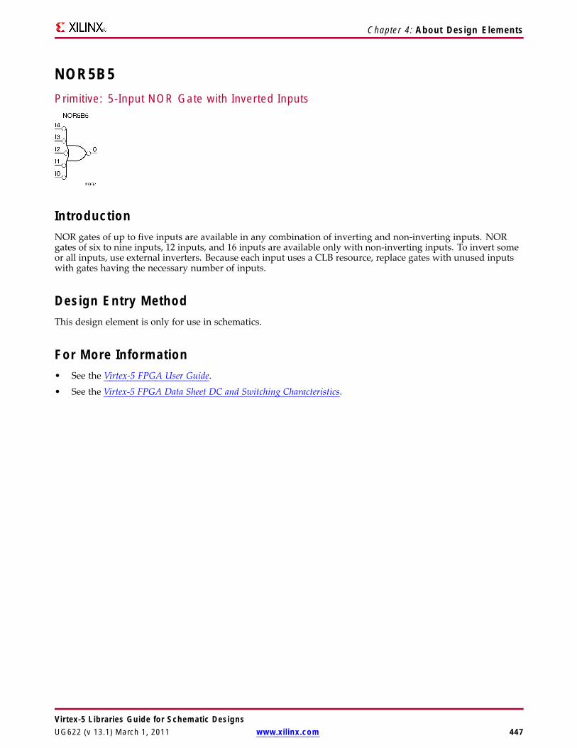
Chapter 4: About Design Elements
NOR5B5Primitive: 5-Input NOR Gate with Inverted Inputs
IntroductionNOR gates of up to five inputs are available in any combination of inverting and non-inverting inputs. NORgates of six to nine inputs, 12 inputs, and 16 inputs are available only with non-inverting inputs. To invert someor all inputs, use external inverters. Because each input uses a CLB resource, replace gates with unused inputswith gates having the necessary number of inputs.
Design Entry MethodThis design element is only for use in schematics.
For More Information• See the Virtex-5 FPGA User Guide.
• See the Virtex-5 FPGA Data Sheet DC and Switching Characteristics.
Virtex-5 Libraries Guide for Schematic DesignsUG622 (v 13.1) March 1, 2011 www.xilinx.com 447
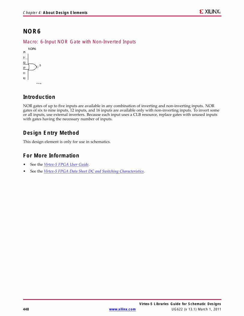
Chapter 4: About Design Elements
NOR6Macro: 6-Input NOR Gate with Non-Inverted Inputs
IntroductionNOR gates of up to five inputs are available in any combination of inverting and non-inverting inputs. NORgates of six to nine inputs, 12 inputs, and 16 inputs are available only with non-inverting inputs. To invert someor all inputs, use external inverters. Because each input uses a CLB resource, replace gates with unused inputswith gates having the necessary number of inputs.
Design Entry MethodThis design element is only for use in schematics.
For More Information• See the Virtex-5 FPGA User Guide.
• See the Virtex-5 FPGA Data Sheet DC and Switching Characteristics.
Virtex-5 Libraries Guide for Schematic Designs448 www.xilinx.com UG622 (v 13.1) March 1, 2011
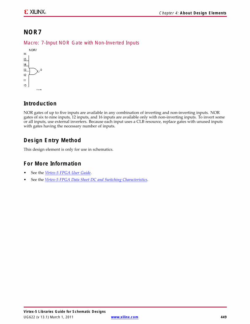
Chapter 4: About Design Elements
NOR7Macro: 7-Input NOR Gate with Non-Inverted Inputs
IntroductionNOR gates of up to five inputs are available in any combination of inverting and non-inverting inputs. NORgates of six to nine inputs, 12 inputs, and 16 inputs are available only with non-inverting inputs. To invert someor all inputs, use external inverters. Because each input uses a CLB resource, replace gates with unused inputswith gates having the necessary number of inputs.
Design Entry MethodThis design element is only for use in schematics.
For More Information• See the Virtex-5 FPGA User Guide.
• See the Virtex-5 FPGA Data Sheet DC and Switching Characteristics.
Virtex-5 Libraries Guide for Schematic DesignsUG622 (v 13.1) March 1, 2011 www.xilinx.com 449
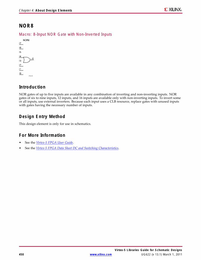
Chapter 4: About Design Elements
NOR8Macro: 8-Input NOR Gate with Non-Inverted Inputs
IntroductionNOR gates of up to five inputs are available in any combination of inverting and non-inverting inputs. NORgates of six to nine inputs, 12 inputs, and 16 inputs are available only with non-inverting inputs. To invert someor all inputs, use external inverters. Because each input uses a CLB resource, replace gates with unused inputswith gates having the necessary number of inputs.
Design Entry MethodThis design element is only for use in schematics.
For More Information• See the Virtex-5 FPGA User Guide.
• See the Virtex-5 FPGA Data Sheet DC and Switching Characteristics.
Virtex-5 Libraries Guide for Schematic Designs450 www.xilinx.com UG622 (v 13.1) March 1, 2011
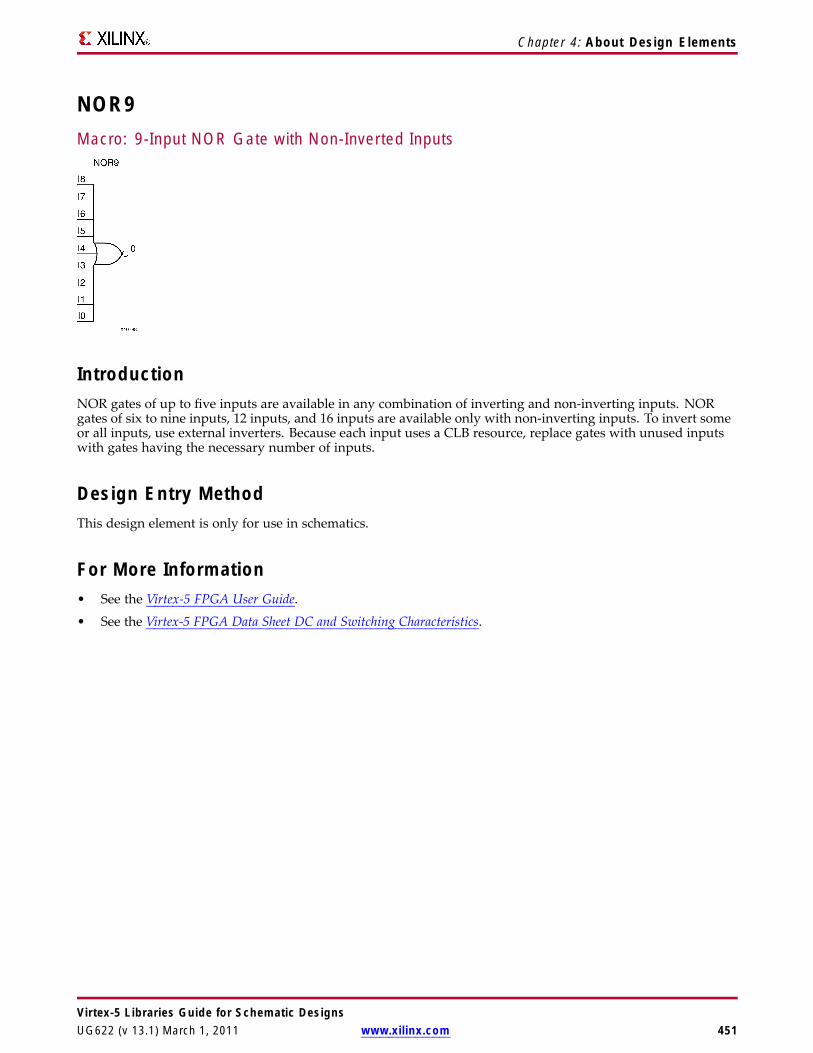
Chapter 4: About Design Elements
NOR9Macro: 9-Input NOR Gate with Non-Inverted Inputs
IntroductionNOR gates of up to five inputs are available in any combination of inverting and non-inverting inputs. NORgates of six to nine inputs, 12 inputs, and 16 inputs are available only with non-inverting inputs. To invert someor all inputs, use external inverters. Because each input uses a CLB resource, replace gates with unused inputswith gates having the necessary number of inputs.
Design Entry MethodThis design element is only for use in schematics.
For More Information• See the Virtex-5 FPGA User Guide.
• See the Virtex-5 FPGA Data Sheet DC and Switching Characteristics.
Virtex-5 Libraries Guide for Schematic DesignsUG622 (v 13.1) March 1, 2011 www.xilinx.com 451

Chapter 4: About Design Elements
OBUFPrimitive: Output Buffer
IntroductionThis design element is a simple output buffer used to drive output signals to the FPGA device pins that do notneed to be 3-stated (constantly driven). Either an OBUF, OBUFT, OBUFDS, or OBUFTDS must be connected toevery output port in the design.
This element isolates the internal circuit and provides drive current for signals leaving a chip. It exists ininput/output blocks (IOB). Its output (O) is connected to an OPAD or an IOPAD. The interface standard usedby this element is LVTTL. Also, this element has selectable drive and slew rates using the DRIVE and SLOWor FAST constraints. The defaults are DRIVE=12 mA and SLOW slew.
Port DescriptionsPort Direction Width FunctionO Output 1 Output of OBUF to be connected directly to top-level output
port.
I Input 1 Input of OBUF. Connect to the logic driving the output port.
Design Entry MethodThis design element can be used in schematics.
Available AttributesAttribute Type Allowed Values Default DescriptionDRIVE Integer 2, 4, 6, 8, 12, 16, 24 12 Specifies the output current drive strength of
the I/O. It is suggested that you set this to thelowest setting tolerable for the design driveand timing requirements.
IOSTANDARD String See Data Sheet "DEFAULT" Assigns an I/O standard to the element.
SLEW String "SLOW" or "FAST" "SLOW" Specifies the slew rate of the outputdriver. Consult the product Data Sheet forrecommendations of the best setting for thisattribute.
For More Information• See the Virtex-5 FPGA User Guide.
• See the Virtex-5 FPGA Data Sheet DC and Switching Characteristics.
Virtex-5 Libraries Guide for Schematic Designs452 www.xilinx.com UG622 (v 13.1) March 1, 2011
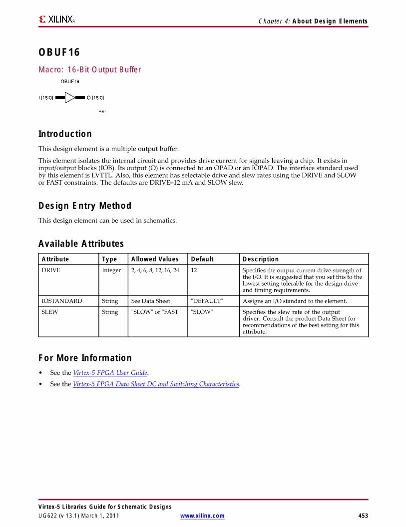
Chapter 4: About Design Elements
OBUF16Macro: 16-Bit Output Buffer
IntroductionThis design element is a multiple output buffer.
This element isolates the internal circuit and provides drive current for signals leaving a chip. It exists ininput/output blocks (IOB). Its output (O) is connected to an OPAD or an IOPAD. The interface standard usedby this element is LVTTL. Also, this element has selectable drive and slew rates using the DRIVE and SLOWor FAST constraints. The defaults are DRIVE=12 mA and SLOW slew.
Design Entry MethodThis design element can be used in schematics.
Available AttributesAttribute Type Allowed Values Default DescriptionDRIVE Integer 2, 4, 6, 8, 12, 16, 24 12 Specifies the output current drive strength of
the I/O. It is suggested that you set this to thelowest setting tolerable for the design driveand timing requirements.
IOSTANDARD String See Data Sheet "DEFAULT" Assigns an I/O standard to the element.
SLEW String "SLOW" or "FAST" "SLOW" Specifies the slew rate of the outputdriver. Consult the product Data Sheet forrecommendations of the best setting for thisattribute.
For More Information• See the Virtex-5 FPGA User Guide.
• See the Virtex-5 FPGA Data Sheet DC and Switching Characteristics.
Virtex-5 Libraries Guide for Schematic DesignsUG622 (v 13.1) March 1, 2011 www.xilinx.com 453
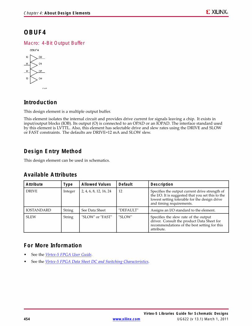
Chapter 4: About Design Elements
OBUF4Macro: 4-Bit Output Buffer
IntroductionThis design element is a multiple output buffer.
This element isolates the internal circuit and provides drive current for signals leaving a chip. It exists ininput/output blocks (IOB). Its output (O) is connected to an OPAD or an IOPAD. The interface standard usedby this element is LVTTL. Also, this element has selectable drive and slew rates using the DRIVE and SLOWor FAST constraints. The defaults are DRIVE=12 mA and SLOW slew.
Design Entry MethodThis design element can be used in schematics.
Available AttributesAttribute Type Allowed Values Default DescriptionDRIVE Integer 2, 4, 6, 8, 12, 16, 24 12 Specifies the output current drive strength of
the I/O. It is suggested that you set this to thelowest setting tolerable for the design driveand timing requirements.
IOSTANDARD String See Data Sheet "DEFAULT" Assigns an I/O standard to the element.
SLEW String "SLOW" or "FAST" "SLOW" Specifies the slew rate of the outputdriver. Consult the product Data Sheet forrecommendations of the best setting for thisattribute.
For More Information• See the Virtex-5 FPGA User Guide.
• See the Virtex-5 FPGA Data Sheet DC and Switching Characteristics.
Virtex-5 Libraries Guide for Schematic Designs454 www.xilinx.com UG622 (v 13.1) March 1, 2011

Chapter 4: About Design Elements
OBUF8Macro: 8-Bit Output Buffer
IntroductionThis design element is a multiple output buffer.
This element isolates the internal circuit and provides drive current for signals leaving a chip. It exists ininput/output blocks (IOB). Its output (O) is connected to an OPAD or an IOPAD. The interface standard usedby this element is LVTTL. Also, this element has selectable drive and slew rates using the DRIVE and SLOWor FAST constraints. The defaults are DRIVE=12 mA and SLOW slew.
Design Entry MethodThis design element can be used in schematics.
Available AttributesAttribute Type Allowed Values Default DescriptionDRIVE Integer 2, 4, 6, 8, 12, 16, 24 12 Specifies the output current drive strength of
the I/O. It is suggested that you set this to thelowest setting tolerable for the design driveand timing requirements.
IOSTANDARD String See Data Sheet "DEFAULT" Assigns an I/O standard to the element.
SLEW String "SLOW" or "FAST" "SLOW" Specifies the slew rate of the outputdriver. Consult the product Data Sheet forrecommendations of the best setting for thisattribute.
For More Information• See the Virtex-5 FPGA User Guide.
• See the Virtex-5 FPGA Data Sheet DC and Switching Characteristics.
Virtex-5 Libraries Guide for Schematic DesignsUG622 (v 13.1) March 1, 2011 www.xilinx.com 455

Chapter 4: About Design Elements
OBUFDSPrimitive: Differential Signaling Output Buffer
IntroductionThis design element is a single output buffer that supports low-voltage, differential signaling (1.8 v CMOS).OBUFDS isolates the internal circuit and provides drive current for signals leaving the chip. Its output isrepresented as two distinct ports (O and OB), one deemed the "master" and the other the "slave." The master andthe slave are opposite phases of the same logical signal (for example, MYNET and MYNETB).
Logic TableInputs Outputs
I O OB0 0 1
1 1 0
Port DescriptionsPort Direction Width FunctionO Output 1 Diff_p output (connect directly to top level port)
OB Output 1 Diff_n output (connect directly to top level port)
I Input 1 Buffer input
Design Entry MethodThis design element can be used in schematics.
Available Attributes
Attribute TypeAllowedValues Default Description
IOSTANDARD String See Data Sheet "DEFAULT" Assigns an I/O standard to the element.
For More Information• See the Virtex-5 FPGA User Guide.
• See the Virtex-5 FPGA Data Sheet DC and Switching Characteristics.
Virtex-5 Libraries Guide for Schematic Designs456 www.xilinx.com UG622 (v 13.1) March 1, 2011

Chapter 4: About Design Elements
OBUFTPrimitive: 3-State Output Buffer with Active Low Output Enable
IntroductionThis design element is a single, 3-state output buffer with input I, output O, and active-Low output enables (T).This element uses the LVTTL standard and has selectable drive and slew rates using the DRIVE and SLOW orFAST constraints. The defaults are DRIVE=12 mA and SLOW slew.
When T is Low, data on the inputs of the buffers is transferred to the corresponding outputs. When T is High, theoutput is high impedance (off or Z state). OBUFTs are generally used when a single-ended output is neededwith a 3-state capability, such as the case when building bidirectional I/O.
Logic TableInputs Outputs
T I O1 X Z
0 1 1
0 0 0
Port DescriptionsPort Direction Width FunctionO Output 1 Buffer output (connect directly to top-level port)
I Input 1 Buffer input
T Input 1 3-state enable input
Design Entry MethodThis design element can be used in schematics.
Available AttributesAttribute Type Allowed Values Default DescriptionDRIVE Integer 2, 4, 6, 8, 12, 16, 24 12 Specifies the output current drive strength
of the I/O. It is suggested that you set thisto the lowest setting tolerable for the designdrive and timing requirements.
IOSTANDARD String See Data Sheet "DEFAULT" Assigns an I/O standard to the element.
SLEW String "SLOW" or "FAST” "SLOW" Specifies the slew rate of the output driver.See the Data Sheet for recommendations ofthe best setting for this attribute.
Virtex-5 Libraries Guide for Schematic DesignsUG622 (v 13.1) March 1, 2011 www.xilinx.com 457

Chapter 4: About Design Elements
For More Information• See the Virtex-5 FPGA User Guide.
• See the Virtex-5 FPGA Data Sheet DC and Switching Characteristics.
Virtex-5 Libraries Guide for Schematic Designs458 www.xilinx.com UG622 (v 13.1) March 1, 2011

Chapter 4: About Design Elements
OBUFT16Macro: 16-Bit 3-State Output Buffer with Active Low Output Enable
IntroductionThis design element is a multiple, 3-state output buffer with input I, output O, and active-Low output enables(T). This element uses the LVTTL standard and has selectable drive and slew rates using the DRIVE and SLOWor FAST constraints. The defaults are DRIVE=12 mA and SLOW slew.
When T is Low, data on the inputs of the buffers is transferred to the corresponding outputs. When T is High, theoutput is high impedance (off or Z state). OBUFTs are generally used when a single-ended output is neededwith a 3-state capability, such as the case when building bidirectional I/O.
Logic TableInputs Outputs
T I O1 X Z
0 1 1
0 0 0
Design Entry MethodThis design element is only for use in schematics.
Available AttributesAttribute Type Allowed Values Default DescriptionDRIVE Integer 2, 4, 6, 8, 12, 16, 24 12 Specifies the output current drive strength
of the I/O. It is suggested that you set thisto the lowest setting tolerable for the designdrive and timing requirements.
IOSTANDARD String See Data Sheet "DEFAULT" Assigns an I/O standard to the element.
SLEW String "SLOW" or "FAST” "SLOW" Specifies the slew rate of the output driver.See the Data Sheet for recommendations ofthe best setting for this attribute.
For More Information• See the Virtex-5 FPGA User Guide.• See the Virtex-5 FPGA Data Sheet DC and Switching Characteristics.
Virtex-5 Libraries Guide for Schematic DesignsUG622 (v 13.1) March 1, 2011 www.xilinx.com 459

Chapter 4: About Design Elements
OBUFT4Macro: 4-Bit 3-State Output Buffers with Active-Low Output Enable
IntroductionThis design element is a multiple, 3-state output buffer with input I, output O, and active-Low output enables(T). This element uses the LVTTL standard and has selectable drive and slew rates using the DRIVE and SLOWor FAST constraints. The defaults are DRIVE=12 mA and SLOW slew.
When T is Low, data on the inputs of the buffers is transferred to the corresponding outputs. When T is High, theoutput is high impedance (off or Z state). OBUFTs are generally used when a single-ended output is neededwith a 3-state capability, such as the case when building bidirectional I/O.
Logic TableInputs Outputs
T I O1 X Z
0 1 1
0 0 0
Design Entry MethodThis design element is only for use in schematics.
Available AttributesAttribute Type Allowed Values Default DescriptionDRIVE Integer 2, 4, 6, 8, 12, 16, 24 12 Specifies the output current drive strength
of the I/O. It is suggested that you set thisto the lowest setting tolerable for the designdrive and timing requirements.
IOSTANDARD String See Data Sheet "DEFAULT" Assigns an I/O standard to the element.
SLEW String "SLOW" or "FAST” "SLOW" Specifies the slew rate of the output driver.See the Data Sheet for recommendations ofthe best setting for this attribute.
Virtex-5 Libraries Guide for Schematic Designs460 www.xilinx.com UG622 (v 13.1) March 1, 2011

Chapter 4: About Design Elements
For More Information• See the Virtex-5 FPGA User Guide.
• See the Virtex-5 FPGA Data Sheet DC and Switching Characteristics.
Virtex-5 Libraries Guide for Schematic DesignsUG622 (v 13.1) March 1, 2011 www.xilinx.com 461

Chapter 4: About Design Elements
OBUFT8Macro: 8-Bit 3-State Output Buffers with Active-Low Output Enable
IntroductionThis design element is a multiple, 3-state output buffer with input I, output O, and active-Low output enables(T). This element uses the LVTTL standard and has selectable drive and slew rates using the DRIVE and SLOWor FAST constraints. The defaults are DRIVE=12 mA and SLOW slew.
When T is Low, data on the inputs of the buffers is transferred to the corresponding outputs. When T is High, theoutput is high impedance (off or Z state). OBUFTs are generally used when a single-ended output is neededwith a 3-state capability, such as the case when building bidirectional I/O.
Logic TableInputs Outputs
T I O1 X Z
0 1 1
0 0 0
Design Entry MethodThis design element is only for use in schematics.
Available AttributesAttribute Type Allowed Values Default DescriptionDRIVE Integer 2, 4, 6, 8, 12, 16, 24 12 Specifies the output current drive strength
of the I/O. It is suggested that you set thisto the lowest setting tolerable for the designdrive and timing requirements.
IOSTANDARD String See Data Sheet "DEFAULT" Assigns an I/O standard to the element.
SLEW String "SLOW" or "FAST” "SLOW" Specifies the slew rate of the output driver.See the Data Sheet for recommendations ofthe best setting for this attribute.
For More Information• See the Virtex-5 FPGA User Guide.• See the Virtex-5 FPGA Data Sheet DC and Switching Characteristics.
Virtex-5 Libraries Guide for Schematic Designs462 www.xilinx.com UG622 (v 13.1) March 1, 2011
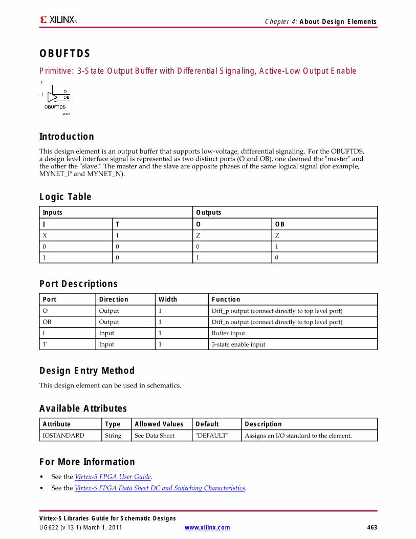
Chapter 4: About Design Elements
OBUFTDSPrimitive: 3-State Output Buffer with Differential Signaling, Active-Low Output Enable
IntroductionThis design element is an output buffer that supports low-voltage, differential signaling. For the OBUFTDS,a design level interface signal is represented as two distinct ports (O and OB), one deemed the "master" andthe other the "slave." The master and the slave are opposite phases of the same logical signal (for example,MYNET_P and MYNET_N).
Logic TableInputs Outputs
I T O OBX 1 Z Z
0 0 0 1
1 0 1 0
Port DescriptionsPort Direction Width FunctionO Output 1 Diff_p output (connect directly to top level port)
OB Output 1 Diff_n output (connect directly to top level port)
I Input 1 Buffer input
T Input 1 3-state enable input
Design Entry MethodThis design element can be used in schematics.
Available AttributesAttribute Type Allowed Values Default DescriptionIOSTANDARD String See Data Sheet "DEFAULT" Assigns an I/O standard to the element.
For More Information• See the Virtex-5 FPGA User Guide.• See the Virtex-5 FPGA Data Sheet DC and Switching Characteristics.
Virtex-5 Libraries Guide for Schematic DesignsUG622 (v 13.1) March 1, 2011 www.xilinx.com 463

Chapter 4: About Design Elements
ODDRPrimitive: Dedicated Dual Data Rate (DDR) Output Register
IntroductionThis design element is a dedicated output register for use in transmitting dual data rate (DDR) signals fromFPGA devices. The ODDR primitive’s interface with the FPGA fabric are not limited to opposite edges. TheODDR is available with modes that allow data to be presented from the FPGA fabric at the same clock edge. Thisfeature allows designers to avoid additional timing complexities and CLB usage. In addition, the ODDR worksin conjunction with SelectIO™ features.
ODDR Modes
This element has two modes of operation. These modes are set by the DDR_CLK_EDGE attribute.
• OPPOSITE_EDGE mode - The data transmit interface uses the classic DDR methodology. Given a data andclock at pin D1-2 and C respectively, D1 is sampled at every positive edge of clock C, and D2 is sampled atevery negative edge of clock C. Q changes every clock edge.
• SAME_EDGE mode - Data is still transmitted at the output of the ODDR by opposite edges of clock C.However, the two inputs to the ODDR are clocked with a positive clock edge of clock signal C and an extraregister is clocked with a negative clock edge of clock signal C. Using this feature, DDR data can now bepresented into the ODDR at the same clock edge.
Port DescriptionsPort Type Width FunctionQ Output 1 Data Output (DDR) - The ODDR output that connects to the IOB
pad.
C Input 1 Clock Input - The C pin represents the clock input pin.
CE Input 1 Clock Enable Input - When asserted High, this port enables theclock input on port C.
D1 : D2 Input 1 (each) Data Input - This pin is where the DDR data is presented intothe ODDR module.
R Input 1 Reset - Depends on how SRTYPE is set.
S Input 1 Set - Active High asynchronous set pin. This pin can also beSynchronous depending on the SRTYPE attribute.
Design Entry MethodThis design element can be used in schematics.
Virtex-5 Libraries Guide for Schematic Designs464 www.xilinx.com UG622 (v 13.1) March 1, 2011

Chapter 4: About Design Elements
Available AttributesAttribute Type Allowed Values Default DescriptionDDR_CLK_EDGE
String "OPPOSITE_EDGE","SAME_EDGE"
"OPPOSITE_EDGE"
DDR clock mode recovery modeselection.
INIT Integer 0, 1 1 Q initialization value.
SRTYPE String "SYNC", "ASYNC" "SYNC" Set/Reset type selection.
For More Information• See the Virtex-5 FPGA User Guide.
• See the Virtex-5 FPGA Data Sheet DC and Switching Characteristics.
Virtex-5 Libraries Guide for Schematic DesignsUG622 (v 13.1) March 1, 2011 www.xilinx.com 465

Chapter 4: About Design Elements
OFDMacro: Output D Flip-Flop
IntroductionThis design element is a single output D flip-flop.
The outputs are connected to OPADs or IOPADs. The data on the (D) inputs is loaded into the flip-flops duringthe Low-to-High clock (C) transition and appears on the (Q) outputs.
This flip-flop is asynchronously cleared, outputs Low, when power is applied. For FPGA devices, power-onconditions are simulated when global set/reset (GSR) is active. GSR defaults to active-High but can be invertedby adding an inverter in front of the GSR input of the appropriate STARTUP_architecture symbol.
Logic TableInputs Outputs
D C QD ↑ D
Design Entry MethodThis design element is only for use in schematics.
For More Information• See the Virtex-5 FPGA User Guide.
• See the Virtex-5 FPGA Data Sheet DC and Switching Characteristics.
Virtex-5 Libraries Guide for Schematic Designs466 www.xilinx.com UG622 (v 13.1) March 1, 2011

Chapter 4: About Design Elements
OFD_1Macro: Output D Flip-Flop with Inverted Clock
IntroductionThe design element is located in an input/output block (IOB). The output (Q) of the D flip-flop is connected to anOPAD or an IOPAD. The data on the (D) input is loaded into the flip-flop during the High-to-Low clock (C)transition and appears on the (Q) output.
This flip-flop is asynchronously cleared, outputs Low, when power is applied. For FPGA devices, power-onconditions are simulated when global set/reset (GSR) is active. GSR defaults to active-High but can be invertedby adding an inverter in front of the GSR input of the appropriate STARTUP_architecture symbol.
Logic TableInputs Outputs
D C QD ↓ D
Design Entry MethodThis design element is only for use in schematics.
For More Information• See the Virtex-5 FPGA User Guide.
• See the Virtex-5 FPGA Data Sheet DC and Switching Characteristics.
Virtex-5 Libraries Guide for Schematic DesignsUG622 (v 13.1) March 1, 2011 www.xilinx.com 467

Chapter 4: About Design Elements
OFD16Macro: 16-Bit Output D Flip-Flop
IntroductionThis design element is a multiple output D flip-flop.
The outputs are connected to OPADs or IOPADs. The data on the (D) inputs is loaded into the flip-flops duringthe Low-to-High clock (C) transition and appears on the (Q) outputs.
This flip-flop is asynchronously cleared, outputs Low, when power is applied. For FPGA devices, power-onconditions are simulated when global set/reset (GSR) is active. GSR defaults to active-High but can be invertedby adding an inverter in front of the GSR input of the appropriate STARTUP_architecture symbol.
Logic TableInputs Outputs
D C QD ↑ D
Design Entry MethodThis design element is only for use in schematics.
For More Information• See the Virtex-5 FPGA User Guide.
• See the Virtex-5 FPGA Data Sheet DC and Switching Characteristics.
Virtex-5 Libraries Guide for Schematic Designs468 www.xilinx.com UG622 (v 13.1) March 1, 2011

Chapter 4: About Design Elements
OFD4Macro: 4-Bit Output D Flip-Flop
IntroductionThis design element is a multiple output D flip-flop.
The outputs are connected to OPADs or IOPADs. The data on the (D) inputs is loaded into the flip-flops duringthe Low-to-High clock (C) transition and appears on the (Q) outputs.
This flip-flop is asynchronously cleared, outputs Low, when power is applied. For FPGA devices, power-onconditions are simulated when global set/reset (GSR) is active. GSR defaults to active-High but can be invertedby adding an inverter in front of the GSR input of the appropriate STARTUP_architecture symbol.
Logic TableInputs Outputs
D C QD ↑ D
Design Entry MethodThis design element is only for use in schematics.
For More Information• See the Virtex-5 FPGA User Guide.
• See the Virtex-5 FPGA Data Sheet DC and Switching Characteristics.
Virtex-5 Libraries Guide for Schematic DesignsUG622 (v 13.1) March 1, 2011 www.xilinx.com 469
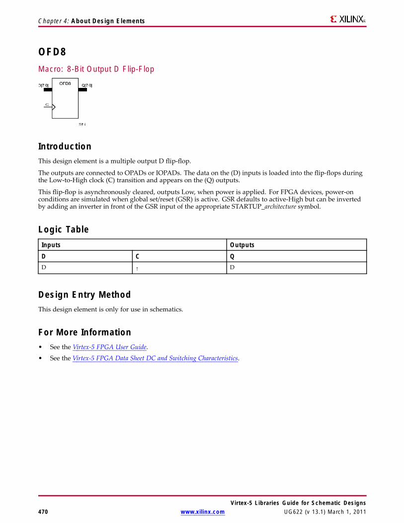
Chapter 4: About Design Elements
OFD8Macro: 8-Bit Output D Flip-Flop
IntroductionThis design element is a multiple output D flip-flop.
The outputs are connected to OPADs or IOPADs. The data on the (D) inputs is loaded into the flip-flops duringthe Low-to-High clock (C) transition and appears on the (Q) outputs.
This flip-flop is asynchronously cleared, outputs Low, when power is applied. For FPGA devices, power-onconditions are simulated when global set/reset (GSR) is active. GSR defaults to active-High but can be invertedby adding an inverter in front of the GSR input of the appropriate STARTUP_architecture symbol.
Logic TableInputs Outputs
D C QD ↑ D
Design Entry MethodThis design element is only for use in schematics.
For More Information• See the Virtex-5 FPGA User Guide.
• See the Virtex-5 FPGA Data Sheet DC and Switching Characteristics.
Virtex-5 Libraries Guide for Schematic Designs470 www.xilinx.com UG622 (v 13.1) March 1, 2011
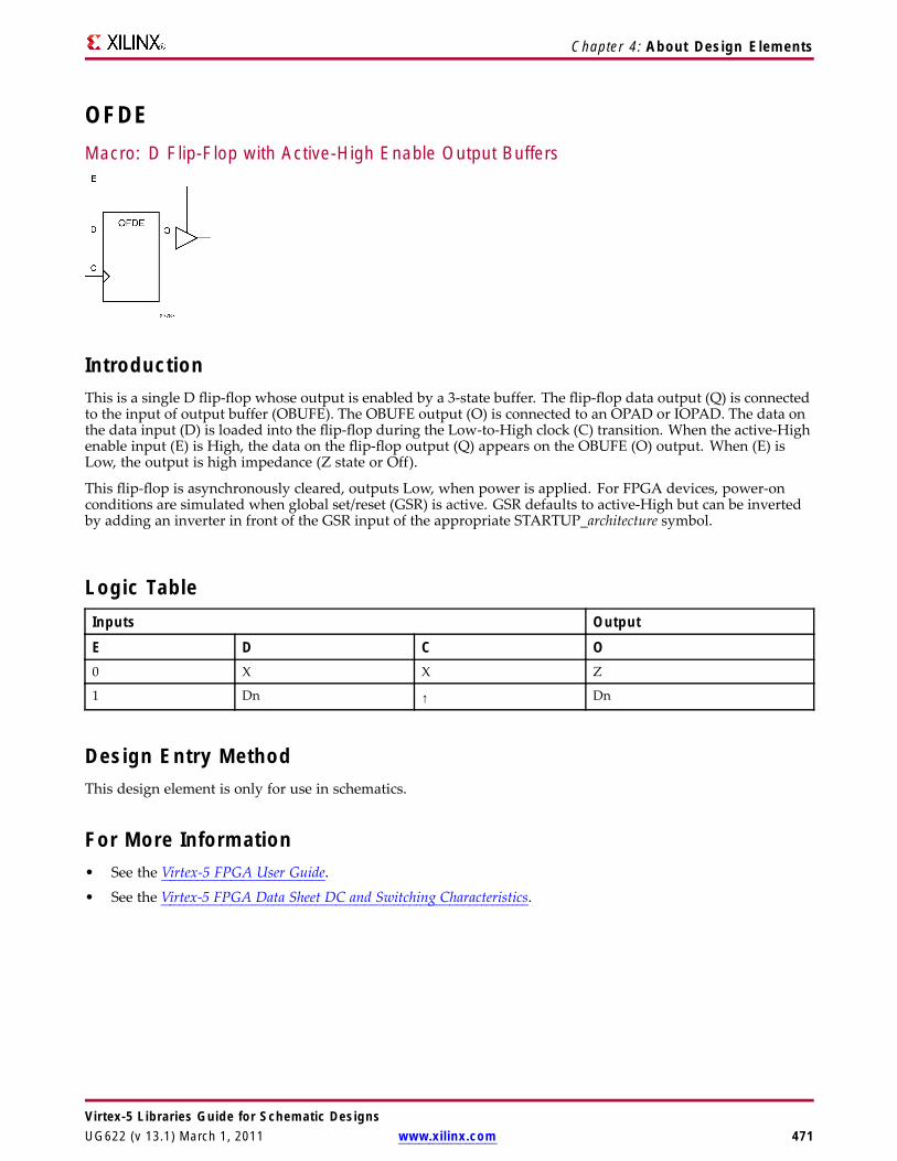
Chapter 4: About Design Elements
OFDEMacro: D Flip-Flop with Active-High Enable Output Buffers
IntroductionThis is a single D flip-flop whose output is enabled by a 3-state buffer. The flip-flop data output (Q) is connectedto the input of output buffer (OBUFE). The OBUFE output (O) is connected to an OPAD or IOPAD. The data onthe data input (D) is loaded into the flip-flop during the Low-to-High clock (C) transition. When the active-Highenable input (E) is High, the data on the flip-flop output (Q) appears on the OBUFE (O) output. When (E) isLow, the output is high impedance (Z state or Off).
This flip-flop is asynchronously cleared, outputs Low, when power is applied. For FPGA devices, power-onconditions are simulated when global set/reset (GSR) is active. GSR defaults to active-High but can be invertedby adding an inverter in front of the GSR input of the appropriate STARTUP_architecture symbol.
Logic TableInputs Output
E D C O0 X X Z
1 Dn ↑ Dn
Design Entry MethodThis design element is only for use in schematics.
For More Information• See the Virtex-5 FPGA User Guide.
• See the Virtex-5 FPGA Data Sheet DC and Switching Characteristics.
Virtex-5 Libraries Guide for Schematic DesignsUG622 (v 13.1) March 1, 2011 www.xilinx.com 471
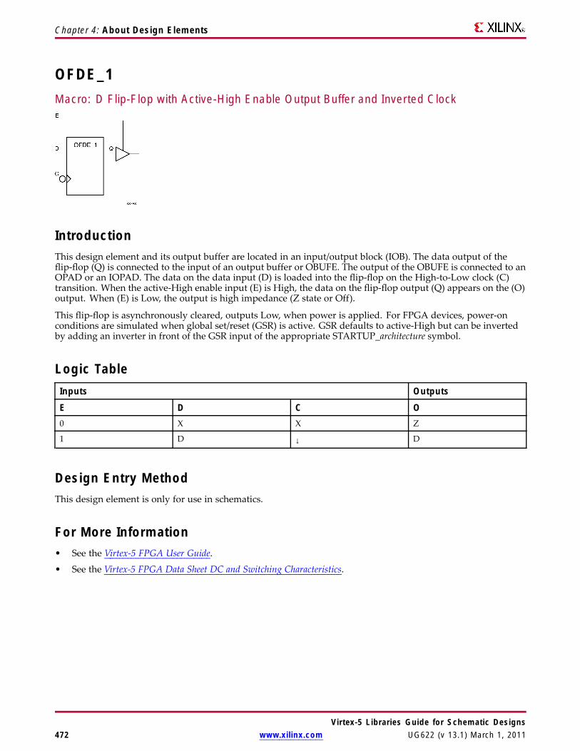
Chapter 4: About Design Elements
OFDE_1Macro: D Flip-Flop with Active-High Enable Output Buffer and Inverted Clock
IntroductionThis design element and its output buffer are located in an input/output block (IOB). The data output of theflip-flop (Q) is connected to the input of an output buffer or OBUFE. The output of the OBUFE is connected to anOPAD or an IOPAD. The data on the data input (D) is loaded into the flip-flop on the High-to-Low clock (C)transition. When the active-High enable input (E) is High, the data on the flip-flop output (Q) appears on the (O)output. When (E) is Low, the output is high impedance (Z state or Off).
This flip-flop is asynchronously cleared, outputs Low, when power is applied. For FPGA devices, power-onconditions are simulated when global set/reset (GSR) is active. GSR defaults to active-High but can be invertedby adding an inverter in front of the GSR input of the appropriate STARTUP_architecture symbol.
Logic TableInputs Outputs
E D C O0 X X Z
1 D ↓ D
Design Entry MethodThis design element is only for use in schematics.
For More Information• See the Virtex-5 FPGA User Guide.
• See the Virtex-5 FPGA Data Sheet DC and Switching Characteristics.
Virtex-5 Libraries Guide for Schematic Designs472 www.xilinx.com UG622 (v 13.1) March 1, 2011

Chapter 4: About Design Elements
OFDE16Macro: 16-Bit D Flip-Flop with Active-High Enable Output Buffers
IntroductionThis is a multiple D flip-flop whose outputs are enabled by 3-state buffers. The flip-flop data outputs (Q) areconnected to the inputs of output buffers (OBUFE). The OBUFE outputs (O) are connected to OPADs or IOPADs.The data on the data inputs (D) is loaded into the flip-flops during the Low-to-High clock (C) transition. Whenthe active-High enable inputs (E) are High, the data on the flip-flop outputs (Q) appears on the OBUFE outputs(O). When (E) is Low, outputs are high impedance (Z state or Off).
This flip-flop is asynchronously cleared, outputs Low, when power is applied. For FPGA devices, power-onconditions are simulated when global set/reset (GSR) is active. GSR defaults to active-High but can be invertedby adding an inverter in front of the GSR input of the appropriate STARTUP_architecture symbol.
Logic TableInputs Outputs
E D C O0 X X Z
1 Dn ↑ Dn
Design Entry MethodThis design element is only for use in schematics.
For More Information• See the Virtex-5 FPGA User Guide.
• See the Virtex-5 FPGA Data Sheet DC and Switching Characteristics.
Virtex-5 Libraries Guide for Schematic DesignsUG622 (v 13.1) March 1, 2011 www.xilinx.com 473
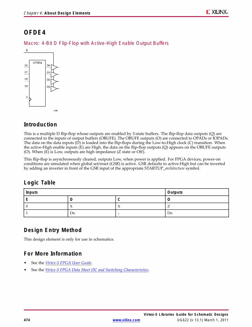
Chapter 4: About Design Elements
OFDE4Macro: 4-Bit D Flip-Flop with Active-High Enable Output Buffers
IntroductionThis is a multiple D flip-flop whose outputs are enabled by 3-state buffers. The flip-flop data outputs (Q) areconnected to the inputs of output buffers (OBUFE). The OBUFE outputs (O) are connected to OPADs or IOPADs.The data on the data inputs (D) is loaded into the flip-flops during the Low-to-High clock (C) transition. Whenthe active-High enable inputs (E) are High, the data on the flip-flop outputs (Q) appears on the OBUFE outputs(O). When (E) is Low, outputs are high impedance (Z state or Off).
This flip-flop is asynchronously cleared, outputs Low, when power is applied. For FPGA devices, power-onconditions are simulated when global set/reset (GSR) is active. GSR defaults to active-High but can be invertedby adding an inverter in front of the GSR input of the appropriate STARTUP_architecture symbol.
Logic TableInputs Outputs
E D C O0 X X Z
1 Dn ↑ Dn
Design Entry MethodThis design element is only for use in schematics.
For More Information• See the Virtex-5 FPGA User Guide.
• See the Virtex-5 FPGA Data Sheet DC and Switching Characteristics.
Virtex-5 Libraries Guide for Schematic Designs474 www.xilinx.com UG622 (v 13.1) March 1, 2011

Chapter 4: About Design Elements
OFDE8Macro: 8-Bit D Flip-Flop with Active-High Enable Output Buffers
IntroductionThis is a multiple D flip-flop whose outputs are enabled by 3-state buffers. The flip-flop data outputs (Q) areconnected to the inputs of output buffers (OBUFE). The OBUFE outputs (O) are connected to OPADs or IOPADs.The data on the data inputs (D) is loaded into the flip-flops during the Low-to-High clock (C) transition. Whenthe active-High enable inputs (E) are High, the data on the flip-flop outputs (Q) appears on the OBUFE outputs(O). When (E) is Low, outputs are high impedance (Z state or Off).
This flip-flop is asynchronously cleared, outputs Low, when power is applied. For FPGA devices, power-onconditions are simulated when global set/reset (GSR) is active. GSR defaults to active-High but can be invertedby adding an inverter in front of the GSR input of the appropriate STARTUP_architecture symbol.
Logic TableInputs Outputs
E D C O0 X X Z
1 Dn ↑ Dn
Design Entry MethodThis design element is only for use in schematics.
For More Information• See the Virtex-5 FPGA User Guide.
• See the Virtex-5 FPGA Data Sheet DC and Switching Characteristics.
Virtex-5 Libraries Guide for Schematic DesignsUG622 (v 13.1) March 1, 2011 www.xilinx.com 475
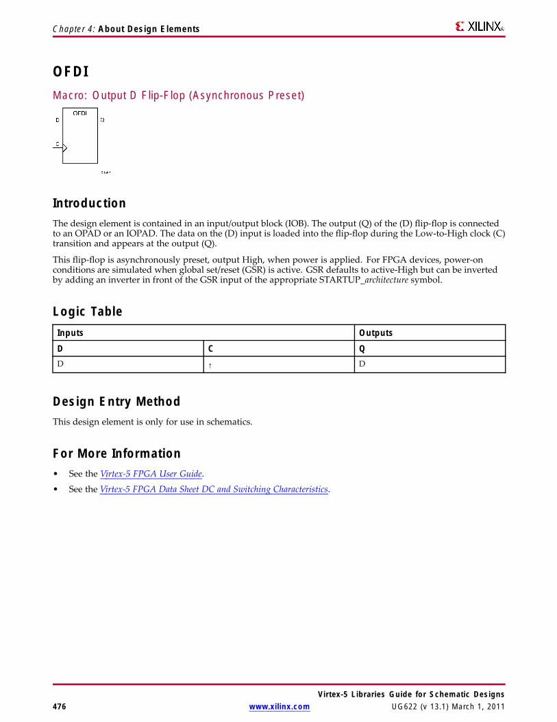
Chapter 4: About Design Elements
OFDIMacro: Output D Flip-Flop (Asynchronous Preset)
IntroductionThe design element is contained in an input/output block (IOB). The output (Q) of the (D) flip-flop is connectedto an OPAD or an IOPAD. The data on the (D) input is loaded into the flip-flop during the Low-to-High clock (C)transition and appears at the output (Q).
This flip-flop is asynchronously preset, output High, when power is applied. For FPGA devices, power-onconditions are simulated when global set/reset (GSR) is active. GSR defaults to active-High but can be invertedby adding an inverter in front of the GSR input of the appropriate STARTUP_architecture symbol.
Logic TableInputs Outputs
D C QD ↑ D
Design Entry MethodThis design element is only for use in schematics.
For More Information• See the Virtex-5 FPGA User Guide.
• See the Virtex-5 FPGA Data Sheet DC and Switching Characteristics.
Virtex-5 Libraries Guide for Schematic Designs476 www.xilinx.com UG622 (v 13.1) March 1, 2011

Chapter 4: About Design Elements
OFDI_1Macro: Output D Flip-Flop with Inverted Clock (Asynchronous Preset)
IntroductionThis design element exists in an input/output block (IOB). The (D) flip-flop output (Q) is connected to an OPADor an IOPAD. The data on the (D) input is loaded into the flip-flop during the High-to-Low clock (C) transitionand appears on the (Q) output.
This flip-flop is asynchronously preset, output High, when power is applied. For FPGA devices, power-onconditions are simulated when global set/reset (GSR) is active. GSR defaults to active-High but can be invertedby adding an inverter in front of the GSR input of the appropriate STARTUP_architecture symbol.
Logic TableInputs Outputs
D C QD ↓ D
Design Entry MethodThis design element is only for use in schematics.
For More Information• See the Virtex-5 FPGA User Guide.
• See the Virtex-5 FPGA Data Sheet DC and Switching Characteristics.
Virtex-5 Libraries Guide for Schematic DesignsUG622 (v 13.1) March 1, 2011 www.xilinx.com 477

Chapter 4: About Design Elements
OFDTMacro: D Flip-Flop with Active-Low 3-State Output Buffer
IntroductionThis design element is a single D flip-flops whose output is enabled by a 3-state buffer.
The data outputs (Q) of the flip-flops are connected to the inputs of output buffers (OBUFT). The outputs of theOBUFTs (O) are connected to OPADs or IOPADs. The data on the data inputs (D) is loaded into the flip-flopsduring the Low-to-High clock (C) transition. When the active-Low enable inputs (T) are Low, the data on theflip-flop outputs (Q) appears on the (O) outputs. When (T) is High, outputs are high impedance (Off).
This flip-flop is asynchronously cleared, outputs Low, when power is applied. For FPGA devices, power-onconditions are simulated when global set/reset (GSR) is active. GSR defaults to active-High but can be invertedby adding an inverter in front of the GSR input of the appropriate STARTUP_architecture symbol.
Logic TableInputs Outputs
T D C O1 X X Z
0 D ↑ D
Design Entry MethodThis design element is only for use in schematics.
For More Information• See the Virtex-5 FPGA User Guide.
• See the Virtex-5 FPGA Data Sheet DC and Switching Characteristics.
Virtex-5 Libraries Guide for Schematic Designs478 www.xilinx.com UG622 (v 13.1) March 1, 2011
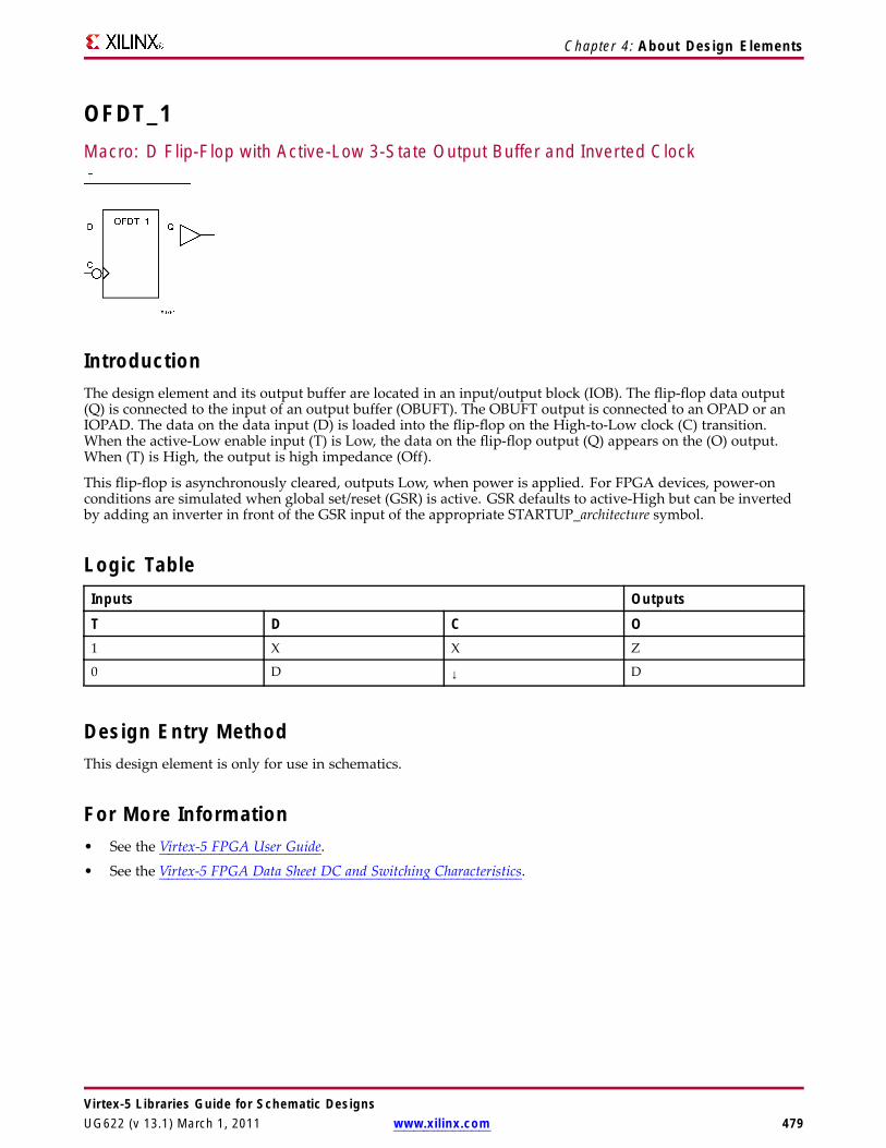
Chapter 4: About Design Elements
OFDT_1Macro: D Flip-Flop with Active-Low 3-State Output Buffer and Inverted Clock
IntroductionThe design element and its output buffer are located in an input/output block (IOB). The flip-flop data output(Q) is connected to the input of an output buffer (OBUFT). The OBUFT output is connected to an OPAD or anIOPAD. The data on the data input (D) is loaded into the flip-flop on the High-to-Low clock (C) transition.When the active-Low enable input (T) is Low, the data on the flip-flop output (Q) appears on the (O) output.When (T) is High, the output is high impedance (Off).
This flip-flop is asynchronously cleared, outputs Low, when power is applied. For FPGA devices, power-onconditions are simulated when global set/reset (GSR) is active. GSR defaults to active-High but can be invertedby adding an inverter in front of the GSR input of the appropriate STARTUP_architecture symbol.
Logic TableInputs Outputs
T D C O1 X X Z
0 D ↓ D
Design Entry MethodThis design element is only for use in schematics.
For More Information• See the Virtex-5 FPGA User Guide.
• See the Virtex-5 FPGA Data Sheet DC and Switching Characteristics.
Virtex-5 Libraries Guide for Schematic DesignsUG622 (v 13.1) March 1, 2011 www.xilinx.com 479

Chapter 4: About Design Elements
OFDT16Macro: 16-Bit D Flip-Flop with Active-Low 3-State Output Buffers
IntroductionThis design element is a multiple D flip-flop whose output are enabled by 3-state buffers.
The data outputs (Q) of the flip-flops are connected to the inputs of output buffers (OBUFT). The outputs of theOBUFTs (O) are connected to OPADs or IOPADs. The data on the data inputs (D) is loaded into the flip-flopsduring the Low-to-High clock (C) transition. When the active-Low enable inputs (T) are Low, the data on theflip-flop outputs (Q) appears on the (O) outputs. When (T) is High, outputs are high impedance (Off).
This flip-flop is asynchronously cleared, outputs Low, when power is applied. For FPGA devices, power-onconditions are simulated when global set/reset (GSR) is active. GSR defaults to active-High but can be invertedby adding an inverter in front of the GSR input of the appropriate STARTUP_architecture symbol.
Logic TableInputs Outputs
T D C O1 X X Z
0 D ↑ D
Design Entry MethodThis design element is only for use in schematics.
For More Information• See the Virtex-5 FPGA User Guide.
• See the Virtex-5 FPGA Data Sheet DC and Switching Characteristics.
Virtex-5 Libraries Guide for Schematic Designs480 www.xilinx.com UG622 (v 13.1) March 1, 2011
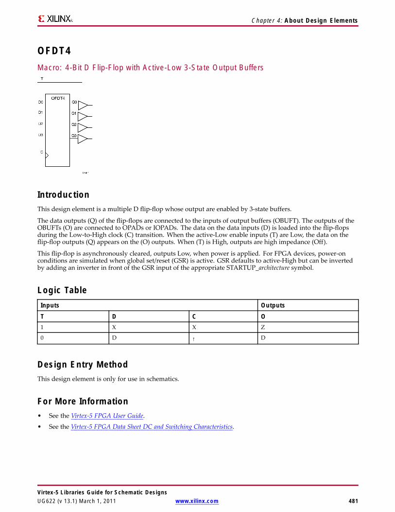
Chapter 4: About Design Elements
OFDT4Macro: 4-Bit D Flip-Flop with Active-Low 3-State Output Buffers
IntroductionThis design element is a multiple D flip-flop whose output are enabled by 3-state buffers.
The data outputs (Q) of the flip-flops are connected to the inputs of output buffers (OBUFT). The outputs of theOBUFTs (O) are connected to OPADs or IOPADs. The data on the data inputs (D) is loaded into the flip-flopsduring the Low-to-High clock (C) transition. When the active-Low enable inputs (T) are Low, the data on theflip-flop outputs (Q) appears on the (O) outputs. When (T) is High, outputs are high impedance (Off).
This flip-flop is asynchronously cleared, outputs Low, when power is applied. For FPGA devices, power-onconditions are simulated when global set/reset (GSR) is active. GSR defaults to active-High but can be invertedby adding an inverter in front of the GSR input of the appropriate STARTUP_architecture symbol.
Logic TableInputs Outputs
T D C O1 X X Z
0 D ↑ D
Design Entry MethodThis design element is only for use in schematics.
For More Information• See the Virtex-5 FPGA User Guide.
• See the Virtex-5 FPGA Data Sheet DC and Switching Characteristics.
Virtex-5 Libraries Guide for Schematic DesignsUG622 (v 13.1) March 1, 2011 www.xilinx.com 481

Chapter 4: About Design Elements
OFDT8Macro: 8-Bit D Flip-Flop with Active-Low 3-State Output Buffers
IntroductionThis design element is a multiple D flip-flop whose output are enabled by 3-state buffers.
The data outputs (Q) of the flip-flops are connected to the inputs of output buffers (OBUFT). The outputs of theOBUFTs (O) are connected to OPADs or IOPADs. The data on the data inputs (D) is loaded into the flip-flopsduring the Low-to-High clock (C) transition. When the active-Low enable inputs (T) are Low, the data on theflip-flop outputs (Q) appears on the (O) outputs. When (T) is High, outputs are high impedance (Off).
This flip-flop is asynchronously cleared, outputs Low, when power is applied. For FPGA devices, power-onconditions are simulated when global set/reset (GSR) is active. GSR defaults to active-High but can be invertedby adding an inverter in front of the GSR input of the appropriate STARTUP_architecture symbol.
Logic TableInputs Outputs
T D C O1 X X Z
0 D ↑ D
Design Entry MethodThis design element is only for use in schematics.
For More Information• See the Virtex-5 FPGA User Guide.
• See the Virtex-5 FPGA Data Sheet DC and Switching Characteristics.
Virtex-5 Libraries Guide for Schematic Designs482 www.xilinx.com UG622 (v 13.1) March 1, 2011

Chapter 4: About Design Elements
OFDXMacro: Output D Flip-Flop with Clock Enable
IntroductionThis design element is a single output D flip-flop. The (Q) output is connected to OPAD or IOPAD. The data onthe (D) input is loaded into the flip-flop during the Low-to-High clock (C) transition and appears on the (Q)output. When (CE) is Low, the flip-flop output does not change.
This flip-flop is asynchronously cleared, outputs Low, when power is applied. For FPGA devices, power-onconditions are simulated when global set/reset (GSR) is active. GSR defaults to active-High but can be invertedby adding an inverter in front of the GSR input of the appropriate STARTUP_architecture symbol.
Logic TableInputs Outputs
CE D C Q1 Dn ↑ Dn
0 X X No change
Design Entry MethodThis design element is only for use in schematics.
For More Information• See the Virtex-5 FPGA User Guide.
• See the Virtex-5 FPGA Data Sheet DC and Switching Characteristics.
Virtex-5 Libraries Guide for Schematic DesignsUG622 (v 13.1) March 1, 2011 www.xilinx.com 483
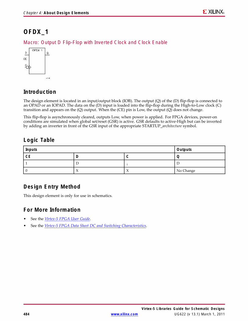
Chapter 4: About Design Elements
OFDX_1Macro: Output D Flip-Flop with Inverted Clock and Clock Enable
IntroductionThe design element is located in an input/output block (IOB). The output (Q) of the (D) flip-flop is connected toan OPAD or an IOPAD. The data on the (D) input is loaded into the flip-flop during the High-to-Low clock (C)transition and appears on the (Q) output. When the (CE) pin is Low, the output (Q) does not change.
This flip-flop is asynchronously cleared, outputs Low, when power is applied. For FPGA devices, power-onconditions are simulated when global set/reset (GSR) is active. GSR defaults to active-High but can be invertedby adding an inverter in front of the GSR input of the appropriate STARTUP_architecture symbol.
Logic TableInputs Outputs
CE D C Q1 D ↓ D
0 X X No Change
Design Entry MethodThis design element is only for use in schematics.
For More Information• See the Virtex-5 FPGA User Guide.
• See the Virtex-5 FPGA Data Sheet DC and Switching Characteristics.
Virtex-5 Libraries Guide for Schematic Designs484 www.xilinx.com UG622 (v 13.1) March 1, 2011

Chapter 4: About Design Elements
OFDX16Macro: 16-Bit Output D Flip-Flop with Clock Enable
IntroductionThis design element is a multiple output D flip-flop. The (Q) output is connected to OPAD or IOPAD. The dataon the (D) input is loaded into the flip-flop during the Low-to-High clock (C) transition and appears on the (Q)output. When (CE) is Low, the flip-flop output does not change.
This flip-flop is asynchronously cleared, outputs Low, when power is applied. For FPGA devices, power-onconditions are simulated when global set/reset (GSR) is active. GSR defaults to active-High but can be invertedby adding an inverter in front of the GSR input of the appropriate STARTUP_architecture symbol.
Logic TableInputs Outputs
CE D C Q1 Dn ↑ Dn
0 X X No change
Design Entry MethodThis design element is only for use in schematics.
For More Information• See the Virtex-5 FPGA User Guide.
• See the Virtex-5 FPGA Data Sheet DC and Switching Characteristics.
Virtex-5 Libraries Guide for Schematic DesignsUG622 (v 13.1) March 1, 2011 www.xilinx.com 485

Chapter 4: About Design Elements
OFDX4Macro: 4-Bit Output D Flip-Flop with Clock Enable
IntroductionThis design element is a multiple output D flip-flop. The (Q) output is connected to OPAD or IOPAD. The dataon the (D) input is loaded into the flip-flop during the Low-to-High clock (C) transition and appears on the (Q)output. When (CE) is Low, the flip-flop output does not change.
This flip-flop is asynchronously cleared, outputs Low, when power is applied. For FPGA devices, power-onconditions are simulated when global set/reset (GSR) is active. GSR defaults to active-High but can be invertedby adding an inverter in front of the GSR input of the appropriate STARTUP_architecture symbol.
Logic TableInputs Outputs
CE D C Q1 Dn ↑ Dn
0 X X No change
Design Entry MethodThis design element is only for use in schematics.
For More Information• See the Virtex-5 FPGA User Guide.
• See the Virtex-5 FPGA Data Sheet DC and Switching Characteristics.
Virtex-5 Libraries Guide for Schematic Designs486 www.xilinx.com UG622 (v 13.1) March 1, 2011

Chapter 4: About Design Elements
OFDX8Macro: 8-Bit Output D Flip-Flop with Clock Enable
IntroductionThis design element is a multiple output D flip-flop. The (Q) output is connected to OPAD or IOPAD. The dataon the (D) input is loaded into the flip-flop during the Low-to-High clock (C) transition and appears on the (Q)output. When (CE) is Low, the flip-flop output does not change.
This flip-flop is asynchronously cleared, outputs Low, when power is applied. For FPGA devices, power-onconditions are simulated when global set/reset (GSR) is active. GSR defaults to active-High but can be invertedby adding an inverter in front of the GSR input of the appropriate STARTUP_architecture symbol.
Logic TableInputs Outputs
CE D C Q1 Dn ↑ Dn
0 X X No change
Design Entry MethodThis design element is only for use in schematics.
For More Information• See the Virtex-5 FPGA User Guide.
• See the Virtex-5 FPGA Data Sheet DC and Switching Characteristics.
Virtex-5 Libraries Guide for Schematic DesignsUG622 (v 13.1) March 1, 2011 www.xilinx.com 487
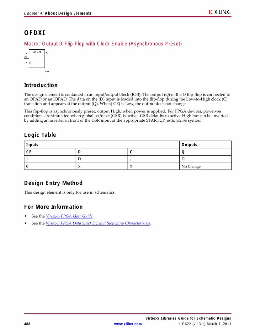
Chapter 4: About Design Elements
OFDXIMacro: Output D Flip-Flop with Clock Enable (Asynchronous Preset)
IntroductionThe design element is contained in an input/output block (IOB). The output (Q) of the D flip-flop is connected toan OPAD or an IOPAD. The data on the (D) input is loaded into the flip-flop during the Low-to-High clock (C)transition and appears at the output (Q). When( CE) is Low, the output does not change
This flip-flop is asynchronously preset, output High, when power is applied. For FPGA devices, power-onconditions are simulated when global set/reset (GSR) is active. GSR defaults to active-High but can be invertedby adding an inverter in front of the GSR input of the appropriate STARTUP_architecture symbol.
Logic TableInputs Outputs
CE D C Q1 D ↑ D
0 X X No Change
Design Entry MethodThis design element is only for use in schematics.
For More Information• See the Virtex-5 FPGA User Guide.
• See the Virtex-5 FPGA Data Sheet DC and Switching Characteristics.
Virtex-5 Libraries Guide for Schematic Designs488 www.xilinx.com UG622 (v 13.1) March 1, 2011

Chapter 4: About Design Elements
OFDXI_1Macro: Output D Flip-Flop with Inverted Clock and Clock Enable (Asynchronous Preset)
IntroductionThe design element is located in an input/output block (IOB). The D flip-flop output (Q) is connected to an OPADor an IOPAD. The data on the D input is loaded into the flip-flop during the High-to-Low clock (C) transition andappears on the Q output. When CE is Low, the output (Q) does not change.
This flip-flop is asynchronously preset, output High, when power is applied. For FPGA devices, power-onconditions are simulated when global set/reset (GSR) is active. GSR defaults to active-High but can be invertedby adding an inverter in front of the GSR input of the appropriate STARTUP_architecture symbol.
Logic TableInputs Outputs
CE D C Q1 D ↓ D
0 X X No Change
Design Entry MethodThis design element is only for use in schematics.
For More Information• See the Virtex-5 FPGA User Guide.
• See the Virtex-5 FPGA Data Sheet DC and Switching Characteristics.
Virtex-5 Libraries Guide for Schematic DesignsUG622 (v 13.1) March 1, 2011 www.xilinx.com 489

Chapter 4: About Design Elements
OR12Macro: 12-Input OR Gate with Non-Inverted Inputs
IntroductionOR functions of up to five inputs are available in any combination of inverting and non-inverting inputs. ORfunctions of six to nine inputs, 12 inputs, and 16 inputs are available with only non-inverting inputs. To invertsome or all inputs, use external inverters. Because each input uses a CLB resource, replace functions with unusedinputs with functions having the necessary number of inputs.
Design Entry MethodThis design element is only for use in schematics.
For More Information• See the Virtex-5 FPGA User Guide.
• See the Virtex-5 FPGA Data Sheet DC and Switching Characteristics.
Virtex-5 Libraries Guide for Schematic Designs490 www.xilinx.com UG622 (v 13.1) March 1, 2011

Chapter 4: About Design Elements
OR16Macro: 16-Input OR Gate with Non-Inverted Inputs
IntroductionOR functions of up to five inputs are available in any combination of inverting and non-inverting inputs. ORfunctions of six to nine inputs, 12 inputs, and 16 inputs are available with only non-inverting inputs. To invertsome or all inputs, use external inverters. Because each input uses a CLB resource, replace functions with unusedinputs with functions having the necessary number of inputs.
Design Entry MethodThis design element is only for use in schematics.
For More Information• See the Virtex-5 FPGA User Guide.
• See the Virtex-5 FPGA Data Sheet DC and Switching Characteristics.
Virtex-5 Libraries Guide for Schematic DesignsUG622 (v 13.1) March 1, 2011 www.xilinx.com 491

Chapter 4: About Design Elements
OR2Primitive: 2-Input OR Gate with Non-Inverted Inputs
IntroductionOR functions of up to five inputs are available in any combination of inverting and non-inverting inputs. ORfunctions of six to nine inputs, 12 inputs, and 16 inputs are available with only non-inverting inputs. To invertsome or all inputs, use external inverters. Because each input uses a CLB resource, replace functions with unusedinputs with functions having the necessary number of inputs.
Design Entry MethodThis design element is only for use in schematics.
For More Information• See the Virtex-5 FPGA User Guide.
• See the Virtex-5 FPGA Data Sheet DC and Switching Characteristics.
Virtex-5 Libraries Guide for Schematic Designs492 www.xilinx.com UG622 (v 13.1) March 1, 2011

Chapter 4: About Design Elements
OR2B1Primitive: 2-Input OR Gate with 1 Inverted and 1 Non-Inverted Inputs
IntroductionOR functions of up to five inputs are available in any combination of inverting and non-inverting inputs. ORfunctions of six to nine inputs, 12 inputs, and 16 inputs are available with only non-inverting inputs. To invertsome or all inputs, use external inverters. Because each input uses a CLB resource, replace functions with unusedinputs with functions having the necessary number of inputs.
Design Entry MethodThis design element is only for use in schematics.
For More Information• See the Virtex-5 FPGA User Guide.
• See the Virtex-5 FPGA Data Sheet DC and Switching Characteristics.
Virtex-5 Libraries Guide for Schematic DesignsUG622 (v 13.1) March 1, 2011 www.xilinx.com 493

Chapter 4: About Design Elements
OR2B2Primitive: 2-Input OR Gate with Inverted Inputs
IntroductionOR functions of up to five inputs are available in any combination of inverting and non-inverting inputs. ORfunctions of six to nine inputs, 12 inputs, and 16 inputs are available with only non-inverting inputs. To invertsome or all inputs, use external inverters. Because each input uses a CLB resource, replace functions with unusedinputs with functions having the necessary number of inputs.
Design Entry MethodThis design element is only for use in schematics.
For More Information• See the Virtex-5 FPGA User Guide.
• See the Virtex-5 FPGA Data Sheet DC and Switching Characteristics.
Virtex-5 Libraries Guide for Schematic Designs494 www.xilinx.com UG622 (v 13.1) March 1, 2011

Chapter 4: About Design Elements
OR3Primitive: 3-Input OR Gate with Non-Inverted Inputs
IntroductionOR functions of up to five inputs are available in any combination of inverting and non-inverting inputs. ORfunctions of six to nine inputs, 12 inputs, and 16 inputs are available with only non-inverting inputs. To invertsome or all inputs, use external inverters. Because each input uses a CLB resource, replace functions with unusedinputs with functions having the necessary number of inputs.
Design Entry MethodThis design element is only for use in schematics.
For More Information• See the Virtex-5 FPGA User Guide.
• See the Virtex-5 FPGA Data Sheet DC and Switching Characteristics.
Virtex-5 Libraries Guide for Schematic DesignsUG622 (v 13.1) March 1, 2011 www.xilinx.com 495

Chapter 4: About Design Elements
OR3B1Primitive: 3-Input OR Gate with 1 Inverted and 2 Non-Inverted Inputs
IntroductionOR functions of up to five inputs are available in any combination of inverting and non-inverting inputs. ORfunctions of six to nine inputs, 12 inputs, and 16 inputs are available with only non-inverting inputs. To invertsome or all inputs, use external inverters. Because each input uses a CLB resource, replace functions with unusedinputs with functions having the necessary number of inputs.
Design Entry MethodThis design element is only for use in schematics.
For More Information• See the Virtex-5 FPGA User Guide.
• See the Virtex-5 FPGA Data Sheet DC and Switching Characteristics.
Virtex-5 Libraries Guide for Schematic Designs496 www.xilinx.com UG622 (v 13.1) March 1, 2011

Chapter 4: About Design Elements
OR3B2Primitive: 3-Input OR Gate with 2 Inverted and 1 Non-Inverted Inputs
IntroductionOR functions of up to five inputs are available in any combination of inverting and non-inverting inputs. ORfunctions of six to nine inputs, 12 inputs, and 16 inputs are available with only non-inverting inputs. To invertsome or all inputs, use external inverters. Because each input uses a CLB resource, replace functions with unusedinputs with functions having the necessary number of inputs.
Design Entry MethodThis design element is only for use in schematics.
For More Information• See the Virtex-5 FPGA User Guide.
• See the Virtex-5 FPGA Data Sheet DC and Switching Characteristics.
Virtex-5 Libraries Guide for Schematic DesignsUG622 (v 13.1) March 1, 2011 www.xilinx.com 497

Chapter 4: About Design Elements
OR3B3Primitive: 3-Input OR Gate with Inverted Inputs
IntroductionOR functions of up to five inputs are available in any combination of inverting and non-inverting inputs. ORfunctions of six to nine inputs, 12 inputs, and 16 inputs are available with only non-inverting inputs. To invertsome or all inputs, use external inverters. Because each input uses a CLB resource, replace functions with unusedinputs with functions having the necessary number of inputs.
Design Entry MethodThis design element is only for use in schematics.
For More Information• See the Virtex-5 FPGA User Guide.
• See the Virtex-5 FPGA Data Sheet DC and Switching Characteristics.
Virtex-5 Libraries Guide for Schematic Designs498 www.xilinx.com UG622 (v 13.1) March 1, 2011

Chapter 4: About Design Elements
OR4Primitive: 4-Input OR Gate with Non-Inverted Inputs
IntroductionOR functions of up to five inputs are available in any combination of inverting and non-inverting inputs. ORfunctions of six to nine inputs, 12 inputs, and 16 inputs are available with only non-inverting inputs. To invertsome or all inputs, use external inverters. Because each input uses a CLB resource, replace functions with unusedinputs with functions having the necessary number of inputs.
Design Entry MethodThis design element is only for use in schematics.
For More Information• See the Virtex-5 FPGA User Guide.
• See the Virtex-5 FPGA Data Sheet DC and Switching Characteristics.
Virtex-5 Libraries Guide for Schematic DesignsUG622 (v 13.1) March 1, 2011 www.xilinx.com 499

Chapter 4: About Design Elements
OR4B1Primitive: 4-Input OR Gate with 1 Inverted and 3 Non-Inverted Inputs
IntroductionOR functions of up to five inputs are available in any combination of inverting and non-inverting inputs. ORfunctions of six to nine inputs, 12 inputs, and 16 inputs are available with only non-inverting inputs. To invertsome or all inputs, use external inverters. Because each input uses a CLB resource, replace functions with unusedinputs with functions having the necessary number of inputs.
Design Entry MethodThis design element is only for use in schematics.
For More Information• See the Virtex-5 FPGA User Guide.
• See the Virtex-5 FPGA Data Sheet DC and Switching Characteristics.
Virtex-5 Libraries Guide for Schematic Designs500 www.xilinx.com UG622 (v 13.1) March 1, 2011
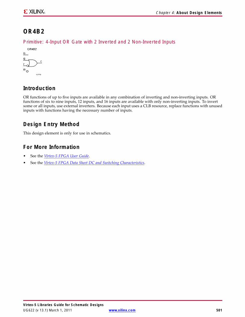
Chapter 4: About Design Elements
OR4B2Primitive: 4-Input OR Gate with 2 Inverted and 2 Non-Inverted Inputs
IntroductionOR functions of up to five inputs are available in any combination of inverting and non-inverting inputs. ORfunctions of six to nine inputs, 12 inputs, and 16 inputs are available with only non-inverting inputs. To invertsome or all inputs, use external inverters. Because each input uses a CLB resource, replace functions with unusedinputs with functions having the necessary number of inputs.
Design Entry MethodThis design element is only for use in schematics.
For More Information• See the Virtex-5 FPGA User Guide.
• See the Virtex-5 FPGA Data Sheet DC and Switching Characteristics.
Virtex-5 Libraries Guide for Schematic DesignsUG622 (v 13.1) March 1, 2011 www.xilinx.com 501

Chapter 4: About Design Elements
OR4B3Primitive: 4-Input OR Gate with 3 Inverted and 1 Non-Inverted Inputs
IntroductionOR functions of up to five inputs are available in any combination of inverting and non-inverting inputs. ORfunctions of six to nine inputs, 12 inputs, and 16 inputs are available with only non-inverting inputs. To invertsome or all inputs, use external inverters. Because each input uses a CLB resource, replace functions with unusedinputs with functions having the necessary number of inputs.
Design Entry MethodThis design element is only for use in schematics.
For More Information• See the Virtex-5 FPGA User Guide.
• See the Virtex-5 FPGA Data Sheet DC and Switching Characteristics.
Virtex-5 Libraries Guide for Schematic Designs502 www.xilinx.com UG622 (v 13.1) March 1, 2011

Chapter 4: About Design Elements
OR4B4Primitive: 4-Input OR Gate with Inverted Inputs
IntroductionOR functions of up to five inputs are available in any combination of inverting and non-inverting inputs. ORfunctions of six to nine inputs, 12 inputs, and 16 inputs are available with only non-inverting inputs. To invertsome or all inputs, use external inverters. Because each input uses a CLB resource, replace functions with unusedinputs with functions having the necessary number of inputs.
Design Entry MethodThis design element is only for use in schematics.
For More Information• See the Virtex-5 FPGA User Guide.
• See the Virtex-5 FPGA Data Sheet DC and Switching Characteristics.
Virtex-5 Libraries Guide for Schematic DesignsUG622 (v 13.1) March 1, 2011 www.xilinx.com 503

Chapter 4: About Design Elements
OR5Primitive: 5-Input OR Gate with Non-Inverted Inputs
IntroductionOR functions of up to five inputs are available in any combination of inverting and non-inverting inputs. ORfunctions of six to nine inputs, 12 inputs, and 16 inputs are available with only non-inverting inputs. To invertsome or all inputs, use external inverters. Because each input uses a CLB resource, replace functions with unusedinputs with functions having the necessary number of inputs.
Design Entry MethodThis design element is only for use in schematics.
For More Information• See the Virtex-5 FPGA User Guide.
• See the Virtex-5 FPGA Data Sheet DC and Switching Characteristics.
Virtex-5 Libraries Guide for Schematic Designs504 www.xilinx.com UG622 (v 13.1) March 1, 2011

Chapter 4: About Design Elements
OR5B1Primitive: 5-Input OR Gate with 1 Inverted and 4 Non-Inverted Inputs
IntroductionOR functions of up to five inputs are available in any combination of inverting and non-inverting inputs. ORfunctions of six to nine inputs, 12 inputs, and 16 inputs are available with only non-inverting inputs. To invertsome or all inputs, use external inverters. Because each input uses a CLB resource, replace functions with unusedinputs with functions having the necessary number of inputs.
Design Entry MethodThis design element is only for use in schematics.
For More Information• See the Virtex-5 FPGA User Guide.
• See the Virtex-5 FPGA Data Sheet DC and Switching Characteristics.
Virtex-5 Libraries Guide for Schematic DesignsUG622 (v 13.1) March 1, 2011 www.xilinx.com 505

Chapter 4: About Design Elements
OR5B2Primitive: 5-Input OR Gate with 2 Inverted and 3 Non-Inverted Inputs
IntroductionOR functions of up to five inputs are available in any combination of inverting and non-inverting inputs. ORfunctions of six to nine inputs, 12 inputs, and 16 inputs are available with only non-inverting inputs. To invertsome or all inputs, use external inverters. Because each input uses a CLB resource, replace functions with unusedinputs with functions having the necessary number of inputs.
Design Entry MethodThis design element is only for use in schematics.
For More Information• See the Virtex-5 FPGA User Guide.
• See the Virtex-5 FPGA Data Sheet DC and Switching Characteristics.
Virtex-5 Libraries Guide for Schematic Designs506 www.xilinx.com UG622 (v 13.1) March 1, 2011
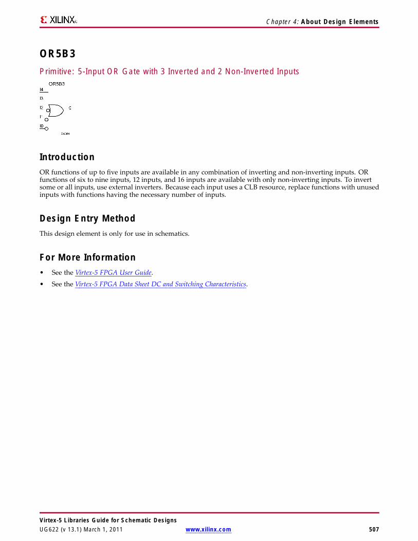
Chapter 4: About Design Elements
OR5B3Primitive: 5-Input OR Gate with 3 Inverted and 2 Non-Inverted Inputs
IntroductionOR functions of up to five inputs are available in any combination of inverting and non-inverting inputs. ORfunctions of six to nine inputs, 12 inputs, and 16 inputs are available with only non-inverting inputs. To invertsome or all inputs, use external inverters. Because each input uses a CLB resource, replace functions with unusedinputs with functions having the necessary number of inputs.
Design Entry MethodThis design element is only for use in schematics.
For More Information• See the Virtex-5 FPGA User Guide.
• See the Virtex-5 FPGA Data Sheet DC and Switching Characteristics.
Virtex-5 Libraries Guide for Schematic DesignsUG622 (v 13.1) March 1, 2011 www.xilinx.com 507

Chapter 4: About Design Elements
OR5B4Primitive: 5-Input OR Gate with 4 Inverted and 1 Non-Inverted Inputs
IntroductionOR functions of up to five inputs are available in any combination of inverting and non-inverting inputs. ORfunctions of six to nine inputs, 12 inputs, and 16 inputs are available with only non-inverting inputs. To invertsome or all inputs, use external inverters. Because each input uses a CLB resource, replace functions with unusedinputs with functions having the necessary number of inputs.
Design Entry MethodThis design element is only for use in schematics.
For More Information• See the Virtex-5 FPGA User Guide.
• See the Virtex-5 FPGA Data Sheet DC and Switching Characteristics.
Virtex-5 Libraries Guide for Schematic Designs508 www.xilinx.com UG622 (v 13.1) March 1, 2011

Chapter 4: About Design Elements
OR5B5Primitive: 5-Input OR Gate with Inverted Inputs
IntroductionOR functions of up to five inputs are available in any combination of inverting and non-inverting inputs. ORfunctions of six to nine inputs, 12 inputs, and 16 inputs are available with only non-inverting inputs. To invertsome or all inputs, use external inverters. Because each input uses a CLB resource, replace functions with unusedinputs with functions having the necessary number of inputs.
Design Entry MethodThis design element is only for use in schematics.
For More Information• See the Virtex-5 FPGA User Guide.
• See the Virtex-5 FPGA Data Sheet DC and Switching Characteristics.
Virtex-5 Libraries Guide for Schematic DesignsUG622 (v 13.1) March 1, 2011 www.xilinx.com 509
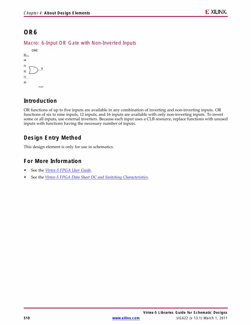
Chapter 4: About Design Elements
OR6Macro: 6-Input OR Gate with Non-Inverted Inputs
IntroductionOR functions of up to five inputs are available in any combination of inverting and non-inverting inputs. ORfunctions of six to nine inputs, 12 inputs, and 16 inputs are available with only non-inverting inputs. To invertsome or all inputs, use external inverters. Because each input uses a CLB resource, replace functions with unusedinputs with functions having the necessary number of inputs.
Design Entry MethodThis design element is only for use in schematics.
For More Information• See the Virtex-5 FPGA User Guide.
• See the Virtex-5 FPGA Data Sheet DC and Switching Characteristics.
Virtex-5 Libraries Guide for Schematic Designs510 www.xilinx.com UG622 (v 13.1) March 1, 2011
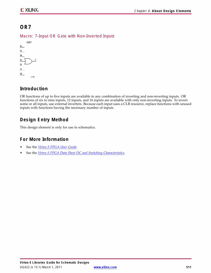
Chapter 4: About Design Elements
OR7Macro: 7-Input OR Gate with Non-Inverted Inputs
IntroductionOR functions of up to five inputs are available in any combination of inverting and non-inverting inputs. ORfunctions of six to nine inputs, 12 inputs, and 16 inputs are available with only non-inverting inputs. To invertsome or all inputs, use external inverters. Because each input uses a CLB resource, replace functions with unusedinputs with functions having the necessary number of inputs.
Design Entry MethodThis design element is only for use in schematics.
For More Information• See the Virtex-5 FPGA User Guide.
• See the Virtex-5 FPGA Data Sheet DC and Switching Characteristics.
Virtex-5 Libraries Guide for Schematic DesignsUG622 (v 13.1) March 1, 2011 www.xilinx.com 511

Chapter 4: About Design Elements
OR8Macro: 8-Input OR Gate with Non-Inverted Inputs
IntroductionOR functions of up to five inputs are available in any combination of inverting and non-inverting inputs. ORfunctions of six to nine inputs, 12 inputs, and 16 inputs are available with only non-inverting inputs. To invertsome or all inputs, use external inverters. Because each input uses a CLB resource, replace functions with unusedinputs with functions having the necessary number of inputs.
Design Entry MethodThis design element is only for use in schematics.
For More Information• See the Virtex-5 FPGA User Guide.
• See the Virtex-5 FPGA Data Sheet DC and Switching Characteristics.
Virtex-5 Libraries Guide for Schematic Designs512 www.xilinx.com UG622 (v 13.1) March 1, 2011

Chapter 4: About Design Elements
OR9Macro: 9-Input OR Gate with Non-Inverted Inputs
IntroductionOR functions of up to five inputs are available in any combination of inverting and non-inverting inputs. ORfunctions of six to nine inputs, 12 inputs, and 16 inputs are available with only non-inverting inputs. To invertsome or all inputs, use external inverters. Because each input uses a CLB resource, replace functions with unusedinputs with functions having the necessary number of inputs.
Design Entry MethodThis design element is only for use in schematics.
For More Information• See the Virtex-5 FPGA User Guide.
• See the Virtex-5 FPGA Data Sheet DC and Switching Characteristics.
Virtex-5 Libraries Guide for Schematic DesignsUG622 (v 13.1) March 1, 2011 www.xilinx.com 513

Chapter 4: About Design Elements
OSERDESPrimitive: Dedicated IOB Output Serializer
IntroductionUse the OSERDES primitive to easily implement a source synchronous interface. This device helps you bysaving logic resources that would otherwise be implemented in the FPGA fabric. It also avoids additionaltiming complexities that you might encounter when you are designing circuitry in the FPGA fabric. Thiselement contains multiple clock inputs to accommodate various applications, and will work in conjunctionwith SelectIO™ features.
Port DescriptionsPort Type Width FunctionOQ Output 1 Data Path Output - This port is the data output of the OSERDES
module. This port connects the output of the data parallel-to-serialconverter to the data input of the IOB pad. In addition, this outputport can also be configured to bypass all the submodules within theOSERDES module.
SHIFTOUT1-2 Output 1 (each) Carry Out for data input expansion. Connect to SHIFTIN1/2 ofmaster.
TQ Output 1 3-State Path Output - This port is the 3-state output of the OSERDESmodule. This port connects the output of the 3-state parallel-to-serialconverter to the control input of the IOB pad.
CLK Input 1 High Speed Clock Input - This clock input is used to drive theparallel-to-serial converters. The possible source for the CLK port isfrom one of the following clock resources:
• Ten global clock lines in a clock region
• Four regional clock lines
Virtex-5 Libraries Guide for Schematic Designs514 www.xilinx.com UG622 (v 13.1) March 1, 2011

Chapter 4: About Design Elements
Port Type Width Function
• Four clock capable I/Os (within adjacent clock region)
• Fabric (through bypass)
CLKDIV Input 1 Divided High Speed Clock Input - This clock input is used to drivethe parallel-to-serial converter. This clock must be a divided downversion of the clock connected to the CLK port. One of the followingclock resources can be used as a source for CLKDIV:
• Ten global clock lines in a clock region
• Four regional clock lines
D1-D6 Input 1 Parallel Data Inputs - Ports D1 to D6 are the location in which allincoming parallel data enters the OSERDES module. This port isconnected to the FPGA fabric, and can be configured from 2 to 6 bits.In the extended width mode, this port can be expanded up to 10 bits.
OCE Input 1 Parallel to serial converter (data) clock enable - This port is usedto enables the output of the data parallel-to-serial converter whenasserted High.
SR Input 1 Set/Reset Input - The set/reset (SR) pin forces the storage elementinto the state specified by the SRVAL attribute. SRVAL = “1”forces a logic 1. SRVAL = “0” forces a logic "0." The reset conditionpredominates over the set condition.
SHIFTIN1-2 Input 1 (each) Carry Input for Data Input Expansion. Connect to SHIFTOUT1/2of slave.
T1 - T4 Input 1 (each) Parallel 3-State Inputs - Ports T1 to T4 are the location in which allparallel 3-state signals enters the OSERDES module. This port isconnected to the FPGA fabric, and can be configured from 1 to 4 bits.This feature is not supported in the extended width mode.
TCE Input 1 Parallel to serial converter (3-state) clock enable - This port is usedto enable the output of the 3-state signal parallel-to-serial converterwhen asserted High.
Design Entry MethodThis design element can be used in schematics.
The data parallel-to-serial converter in the OSERDES module takes in 2 to 6 bits of parallel data and convertsthem into serial data. Data input widths larger than 6 (7, 8, and 10) are achievable by cascading two OSERDESmodules for data width expansion. In order to do this, one OSERDES must be set into a MASTER mode, whileanother is set into SLAVE mode. You must connect the SHIFTOUT of "slave" and SHIFTIN of "master" portstogether. The "slave" only uses D3 to D6 ports as its input. The parallel-to-serial converter is available for bothSDR and DDR modes.
This module is designed such that the data input at D1 port is the first output bit. This module is controlledby CLK and CLKDIV clocks. The following table describes the relationship between CLK and CLKDIV forboth SDR and DDR mode.
Virtex-5 Libraries Guide for Schematic DesignsUG622 (v 13.1) March 1, 2011 www.xilinx.com 515
Chapter 4: About Design Elements
SDR Data Width DDR Data Width CLK CLKDIV2 4 2X X
3 6 3X X
4 8 4X X
5 10 5X X
6 - 6X X
7 - 7X X
8 - 8X X
Output of this block is connected to the data input of an IOB pad of the FPGA. This IOB pad can be configured toa desired standard using SelectIO.
Parallel-to-Serial Converter (3-state)
The 3-state parallel-to-serial converter in the OSERDES module takes in up to 4 bits of parallel 3-state signals andconverts them into serial 3-state signal. Unlike the data parallel-to-serial converter, the 3-state parallel-to-serialconverter is not extendable to more than 4-bit, 3-state signals. This module is primarily controlled by CLK andCLKDIV clocks. In order to use this module, the following attributes must be declared: DATA_RATE_TQ andTRISTATE_WIDTH. In certain cases, you can also need to declare DATA_RATE_OQ and DATA_WIDTH. Thefollowing table lists the attributes needed for the desired functionality.
Mode of Operation DATA_RATE_TQ TRISTATE_WIDTH4-bit DDR* DDR 4
1-bit SDR SDR 1
Buffer BUF 1
Output of this block is connected to the 3-state input of an IOB pad of the FPGA. This IOB pad can be configuredto a desired standard using SelectIO.
Width Expansion
It is possible to use this element to transmit parallel data widths larger than six. However, the 3-state output isnot expandable. In order to use this feature, two of these elements need to be instantiated, and the two must be anadjacent master and slave pair. The attribute MODE must be set to either "MASTER" or "SLAVE" in order todifferentiate the modes of the OSERDES pair. In addition, you must connect the SHIFTIN ports of the MASTERto the SHIFTOUT ports of the SLAVE. This feature supports data widths of 7, 8, and 10 for SDR and DDR mode.The table below lists the data width availability for SDR and DDR mode.
Mode WidthsSDR Data Widths 2,3,4,5,6,7,8
DDR Data Widths 4,6,8,10
Available AttributesAttribute Type Allowed Values Default DescriptionDATA_RATE_OQ String "SDR", "DDR" "DDR" Defines whether the data changes at every
clock edge or every positive clock edgewith respect to CLK.
DATA_RATE_TQ String "BUF", "SDR","DDR"
"DDR" Defines whether the 3-state changes atevery clock edge, every positive clockedge, or buffer configuration with respectto CLK.
Virtex-5 Libraries Guide for Schematic Designs516 www.xilinx.com UG622 (v 13.1) March 1, 2011
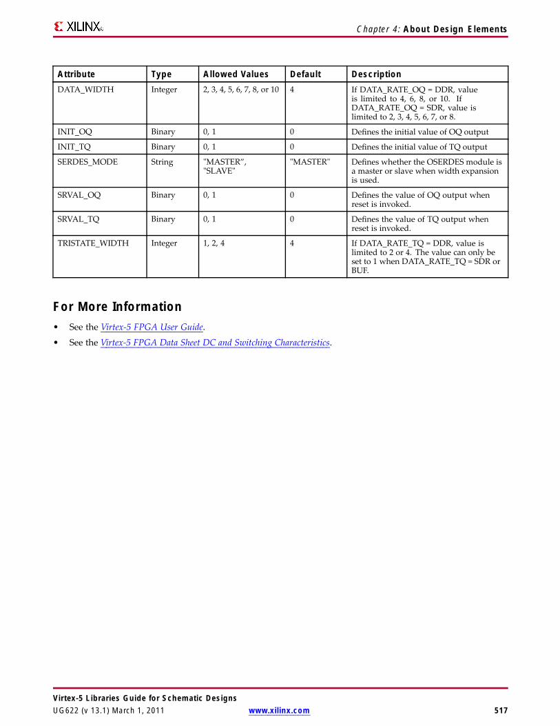
Chapter 4: About Design Elements
Attribute Type Allowed Values Default DescriptionDATA_WIDTH Integer 2, 3, 4, 5, 6, 7, 8, or 10 4 If DATA_RATE_OQ = DDR, value
is limited to 4, 6, 8, or 10. IfDATA_RATE_OQ = SDR, value islimited to 2, 3, 4, 5, 6, 7, or 8.
INIT_OQ Binary 0, 1 0 Defines the initial value of OQ output
INIT_TQ Binary 0, 1 0 Defines the initial value of TQ output
SERDES_MODE String "MASTER”,"SLAVE"
"MASTER" Defines whether the OSERDES module isa master or slave when width expansionis used.
SRVAL_OQ Binary 0, 1 0 Defines the value of OQ output whenreset is invoked.
SRVAL_TQ Binary 0, 1 0 Defines the value of TQ output whenreset is invoked.
TRISTATE_WIDTH Integer 1, 2, 4 4 If DATA_RATE_TQ = DDR, value islimited to 2 or 4. The value can only beset to 1 when DATA_RATE_TQ = SDR orBUF.
For More Information• See the Virtex-5 FPGA User Guide.
• See the Virtex-5 FPGA Data Sheet DC and Switching Characteristics.
Virtex-5 Libraries Guide for Schematic DesignsUG622 (v 13.1) March 1, 2011 www.xilinx.com 517
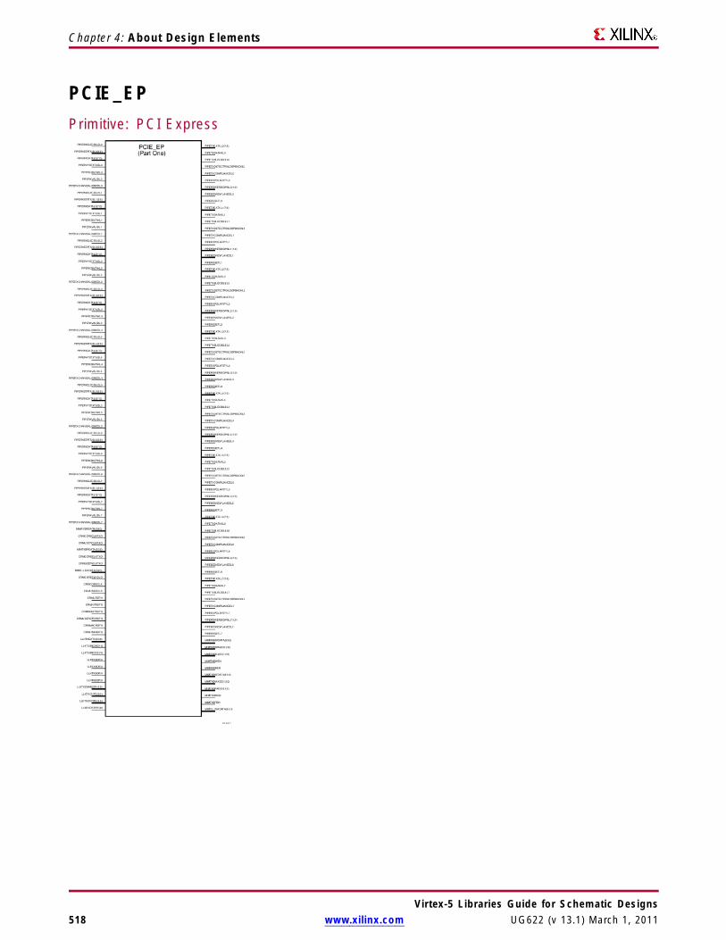
Chapter 4: About Design Elements
PCIE_EPPrimitive: PCI Express
Virtex-5 Libraries Guide for Schematic Designs518 www.xilinx.com UG622 (v 13.1) March 1, 2011

Chapter 4: About Design Elements
IntroductionThis design element is an Integrated Endpoint block embedded in Virtex®-5 devices. It leverages the PCIEXPRESS® (PCIe®) functionality that implements the next-generation evolution of the older PCI™ and PCI-X™parallel bus standards. It is a high-performance, general-purpose interconnect architecture, designed for a widerange of computing and communications platforms. It is a packet-based, point-to-point serial interface that isbackward compatible with PCI and PCI-X configurations, device drivers, and application software.
Design Entry MethodFor More Information• See the Virtex-5 Integrated Endpoint Block for PCI Express Designs User Guide.• See the Virtex-5 FPGA Data Sheet DC and Switching Characteristics.• See the Virtex-5 FPGA User Guide.
Virtex-5 Libraries Guide for Schematic DesignsUG622 (v 13.1) March 1, 2011 www.xilinx.com 519
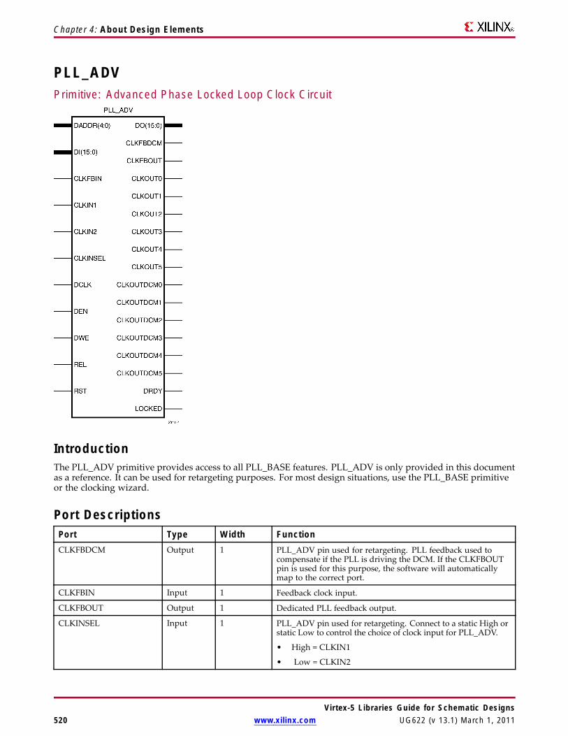
Chapter 4: About Design Elements
PLL_ADVPrimitive: Advanced Phase Locked Loop Clock Circuit
IntroductionThe PLL_ADV primitive provides access to all PLL_BASE features. PLL_ADV is only provided in this documentas a reference. It can be used for retargeting purposes. For most design situations, use the PLL_BASE primitiveor the clocking wizard.
Port DescriptionsPort Type Width FunctionCLKFBDCM Output 1 PLL_ADV pin used for retargeting. PLL feedback used to
compensate if the PLL is driving the DCM. If the CLKFBOUTpin is used for this purpose, the software will automaticallymap to the correct port.
CLKFBIN Input 1 Feedback clock input.
CLKFBOUT Output 1 Dedicated PLL feedback output.
CLKINSEL Input 1 PLL_ADV pin used for retargeting. Connect to a static High orstatic Low to control the choice of clock input for PLL_ADV.
• High = CLKIN1
• Low = CLKIN2
Virtex-5 Libraries Guide for Schematic Designs520 www.xilinx.com UG622 (v 13.1) March 1, 2011
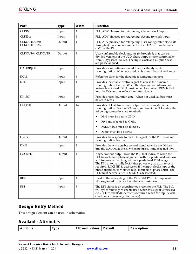
Chapter 4: About Design Elements
Port Type Width FunctionCLKIN1 Input 1 PLL_ADV pin used for retargeting. General clock input.
CLKIN2 Input 1 PLL_ADV pin used for retargeting. Secondary clock input.
CLKOUTDCM0 -CLKOUTDCM5
Output 1 PLL_ADV pin used for retargeting. User configurable clocks (0through 5) that can only connect to the DCM within the sameCMT as the PLL.
CLKOUT0 - CLKOUT5 Output 1 User configurable clock outputs (0 through 5) that can bedivided versions of the VCO phase outputs (user controllable)from 1 (bypassed) to 128. The input clock and output clocksare phase aligned.
DADDR[4:0] Input 5 Provides a reconfiguration address for the dynamicreconfiguration. When not used, all bits must be assigned zeros.
DCLK Input 1 Reference clock for the dynamic reconfiguration port.
DEN Input 1 Provides the enable control signal to access the dynamicreconfiguration feature. When the dynamic reconfigurationfeature is not used, DEN must be tied low. When DEN is tiedlow, the DO outputs reflect the status signals.
DI[15:0] Input 16 Provides reconfiguration data. When not used, all bits mustbe set to zeros.
DO[15:0] Output 16 Provides PLL status or data output when using dynamicreconfiguration. For the DO bus to represent the PLL status, thefollowing connections are required:
• DEN must be tied to GND.
• DWE must be tied to GND.
• DADDR bus must be all zeros.
• DI bus must be all zeros.
DRDY Output 1 Provides the response to the DEN signal for the PLL dynamicreconfiguration feature.
DWE Input 1 Provides the write enable control signal to write the DI datainto the DADDR address. When not used, it must be tied low.
LOCKED Output 1 Asynchronous output from the PLL that indicates when thePLL has achieved phase alignment within a predefined windowand frequency matching within a predefined PPM range.The PLL automatically locks after power on, no extra reset isrequired. LOCKED is deasserted if the input clock stops or thephase alignment is violated (e.g., input clock phase shift). ThePLL must be reset after LOCKED is deasserted.
REL Input 1 Used in the retargeting of the Virtex®-4 PMCD component.Not suggested to be used in other circumstances.
RST Input 1 The RST signal is an asynchronous reset for the PLL. The PLLwill synchronously re-enable itself when this signal is released(i.e., PLL re-enabled). A reset is required when the input clockconditions change (e.g., frequency).
Design Entry MethodThis design element can be used in schematics.
Available AttributesAttribute Type Allowed_Values Default Description
Virtex-5 Libraries Guide for Schematic DesignsUG622 (v 13.1) March 1, 2011 www.xilinx.com 521
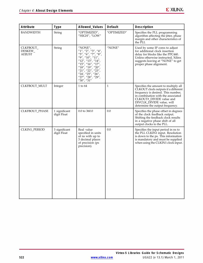
Chapter 4: About Design Elements
Attribute Type Allowed_Values Default DescriptionBANDWIDTH String “OPTIMIZED”,
“HIGH”, “LOW”“OPTIMIZED” Specifies the PLL programming
algorithm affecting the jitter, phasemargin and other characteristics ofthe PLL
CLKFBOUT_DESKEW_ADJUST
String “NONE”,”1”, “2”, “3”, “4”,“5”, “6”, “7”, “8”,“9”, “10”, “11”,“12”, “13”, “14”,“15”, “16”, “17”,“18”, “19”, “20”,“21”, “22”, “23”,“24’, “25”, “26”,“27”, “28”, “29”,“30”, “31”
“NONE” Used by some IP cores to adjustfor additional clock insertiondelay for blocks like the PPC440.Unless otherwise instructed, Xilinxsuggests leaving at “NONE” to getproper phase alignment.
CLKFBOUT_MULT Integer 1 to 64 1 Specifies the amount to multiply allCLKOUT clock outputs if a differentfrequency is desired. This number,in combination with the associatedCLKOUT#_DIVIDE value andDIVCLK_DIVIDE value, willdetermine the output frequency.
CLKFBOUT_PHASE 1 significantdigit Float
0.0 to 360.0 0.0 Specifies the phase offset in degreesof the clock feedback output.Shifting the feedback clock resultsin a negative phase shift of alloutput clocks to the PLL.
CLKIN1_PERIOD 3 significantdigit Float
Real valuespecified in unitsof ns with up to3 decimal placesof precision (psprecision).
0.0 Specifies the input period in ns tothe PLL CLKIN1 input. Resolutionis down to the ps. This informationis mandatory and must be suppliedwhen using the CLKIN1 clock input.
Virtex-5 Libraries Guide for Schematic Designs522 www.xilinx.com UG622 (v 13.1) March 1, 2011

Chapter 4: About Design Elements
Attribute Type Allowed_Values Default DescriptionCLKIN2_PERIOD 3 significant
digit FloatReal valuespecified in unitsof ns with up to3 decimal placesof precision (psprecision).
0.0 Specifies the input period in ns tothe PLL CLKIN2 input. Resolutionis down to the ps. This informationis mandatory and must be suppliedwhen using the CLKIN2 clock input.
CLKOUT0_DESKEW_ADJUST -CLKOUT5_DESKEW_ADJUST
String “NONE”,”1”, “2”, “3”, “4”,“5”, “6”, “7”, “8”,“9”, “10”, “11”,“12”, “13”, “14”,“15”, “16”, “17”,“18”, “19”, “20”,“21”, “22”, “23”,“24’, “25”, “26”,“27”, “28”, “29”,“30”, “31”
“NONE” Parameter to be used in PPC440designs only. For more information,see the section on clock insertiondelays and PLL usage in theEmbedded Processor Block User Guide.
CLKOUT0_DIVIDE -CLKOUT5_DIVIDE
Integer 1 to 128 1 Specifies the amount to divide theassociated CLKOUT clock outputif a different frequency is desired.This number in combinationwith the CLKFBOUT_MULT andDIVCLK_DIVIDE values willdetermine the output frequency.
CLKOUT0_DUTY_CYCLE -CLKOUT5_DUTY_CYCLE
2 significantdigit Float
0.01 to 0.99 0.50 Specifies the Duty Cycle of theassociated CLKOUT clock output inpercentage (i.e., 0.50 will generate a50% duty cycle).
CLKOUT0_PHASE -CLKOUT5_PHASE
1 significantdigit Float
0.0 to 360.0 0.0 Allows specification of the outputphase relationship of the associatedCLKOUT clock output in numberof degrees offset (i.e., 90 indicatesa 90 or 1/4 cycle offset phase offsetwhile 180 indicates a 180 offset or1/2 cycle phase offset).
Virtex-5 Libraries Guide for Schematic DesignsUG622 (v 13.1) March 1, 2011 www.xilinx.com 523

Chapter 4: About Design Elements
Attribute Type Allowed_Values Default DescriptionCOMPENSATION String “SYSTEM_
SYNCHRONOUS”,“SOURCE_SYNCHRONOUS”,"INTERNAL","EXTERNAL","DCM2PLL","PLL2DCM"
“SYSTEM_SYNCHRONOUS”
Specifies the PLL phasecompensation for the incomingclock. SYSTEM_SYNCHRONOUSattempts to compensate allclock delay for 0 hold time.SOURCE_SYNCHRONOUS is usedwhen a clock is provided with dataand thus phased with the clock.Additional attributes automaticallyselected by the ISE software -INTERNAL EXTERNAL DCM2PLLPLL2DCM.
DIVCLK_DIVIDE Integer 1 to 52 1 Specifies the division ratio for alloutput clocks with respect to theinput clock.
EN_REL Boolean FALSE, TRUE FALSE When in PMCD mode(PLL_PMCD_MODE = TRUE),specifies release of divided clockCLKA outputs when the REL inputpin is asserted.
PLL_PMCD_MODE Boolean FALSE, TRUE FALSE Enables PLL to act as PMCDs.
REF_JITTER 3 significantdigit Float
0.000 to 1.000 0.100 Allows specification of the expectedjitter on the reference clock inorder to better optimize PLLperformance. A bandwidth settingof OPTIMIZED will attempt tochoose the best parameter for inputclocking when unknown. If known,then the value provided shouldbe specified in terms of the UIpercentage (the maximum peak topeak value) of the expected jitter onthe input clock.
RESET_ON_LOSS_OF_LOCK
Boolean FALSE, TRUE FALSE Must be set to FALSE, not supportedin silicon.
RST_DEASSERT_CLK
String “CLKIN1”,“CLKFBIN”,
“CLKIN1” Specifies the deassertion of theRST signal to be synchronous to aselected PMCD input clock.
SIM_DEVICE String “VIRTEX5”,“SPARTAN6”
“VIRTEX5” Specifies target device in order toproperly simulate this componentWhen targeting Virtex®-5 must beset to VIRTEX5.
For More Information• See the Virtex-5 FPGA User Guide.
• See the Virtex-5 FPGA Data Sheet DC and Switching Characteristics.
Virtex-5 Libraries Guide for Schematic Designs524 www.xilinx.com UG622 (v 13.1) March 1, 2011
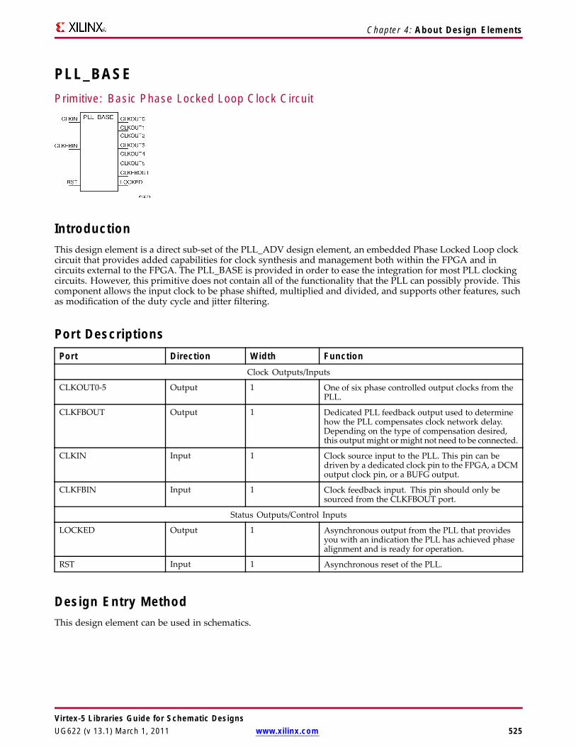
Chapter 4: About Design Elements
PLL_BASEPrimitive: Basic Phase Locked Loop Clock Circuit
IntroductionThis design element is a direct sub-set of the PLL_ADV design element, an embedded Phase Locked Loop clockcircuit that provides added capabilities for clock synthesis and management both within the FPGA and incircuits external to the FPGA. The PLL_BASE is provided in order to ease the integration for most PLL clockingcircuits. However, this primitive does not contain all of the functionality that the PLL can possibly provide. Thiscomponent allows the input clock to be phase shifted, multiplied and divided, and supports other features, suchas modification of the duty cycle and jitter filtering.
Port DescriptionsPort Direction Width Function
Clock Outputs/Inputs
CLKOUT0-5 Output 1 One of six phase controlled output clocks from thePLL.
CLKFBOUT Output 1 Dedicated PLL feedback output used to determinehow the PLL compensates clock network delay.Depending on the type of compensation desired,this output might or might not need to be connected.
CLKIN Input 1 Clock source input to the PLL. This pin can bedriven by a dedicated clock pin to the FPGA, a DCMoutput clock pin, or a BUFG output.
CLKFBIN Input 1 Clock feedback input. This pin should only besourced from the CLKFBOUT port.
Status Outputs/Control Inputs
LOCKED Output 1 Asynchronous output from the PLL that providesyou with an indication the PLL has achieved phasealignment and is ready for operation.
RST Input 1 Asynchronous reset of the PLL.
Design Entry MethodThis design element can be used in schematics.
Virtex-5 Libraries Guide for Schematic DesignsUG622 (v 13.1) March 1, 2011 www.xilinx.com 525

Chapter 4: About Design Elements
Available AttributesAttribute Type Allowed Values Default DescriptionCOMPENSATION String "SYSTEM_
SYNCHRONOUS","SOURCE_SYNCHRONOUS"
"SYSTEM_SYNCHRONOUS"
Specifies the PLL phasecompensation for the incomingclock.SYSTEM_SYNCHRONOUSattempts to compensate all clock delaywhile SOURCE_SYNCHRONOUS isused when a clock is provided withdata and thus phased with the clock.
BANDWIDTH String "HIGH", "LOW","OPTIMIZED"
"OPTIMIZED" Specifies the PLL programmingalgorithm affecting the jitter, phasemargin and other characteristics of thePLL.
CLKOUT0_DIVIDE,CLKOUT1_DIVIDE,CLKOUT2_DIVIDE,CLKOUT3_DIVIDE,CLKOUT4_DIVIDE,CLKOUT5_DIVIDE
Integer 1 to 128 1 Specifies the amount to divide theassociated CLKOUT clock outputif a different frequency is desired.This number in combination with theFBCLKOUT_MULT value determinesthe output frequency.
CLKOUT0_PHASE,CLKOUT1_PHASE,CLKOUT2_PHASE,CLKOUT3_PHASE,CLKOUT4_PHASE,CLKOUT5_PHASE
Real 0.01 to 360.0 0.0 Allows specification of the outputphase relationship of the associatedCLKOUT clock output in number ofdegrees offset (i.e. 90 indicates a 90degree or ¼ cycle offset phase offsetwhile 180 indicates a 180 degree offsetor ½ cycle phase offset).
CLKOUT0_DUTY_CYCLE,CLKOUT1_DUTY_CYCLE,CLKOUT2_DUTY_CYCLE,CLKOUT3_DUTY_CYCLE,CLKOUT4_DUTY_CYCLE,CLKOUT5_DUTY_CYCLE,
Real 0.01 to 0.99 0.50 Specifies the Duty Cycle of theassociated CLKOUT clock output inpercentage (i.e. 0.50 generates a 50%duty cycle).
CLKFBOUT_MULT Integer 1 to 64 1 Specifies the amount to multiply allCLKOUT clock outputs if a differentfrequency is desired. This numberin combination with the associatedCLKOUT#_DIVIDE value determinesthe output frequency.
DIVCLK_DIVIDE Integer 1 to 52 1 Specifies the division ratio for alloutput clocks.
CLKFBOUT_PHASE Real 0.0 to 360 0.0 Specifies the phase offset in degrees ofthe clock feedback output.
REF_JITTER Real 0.000 to 0.999 0.100 The reference clock jitter is specified interms of the UI which is a percentageof the reference clock. The numberprovided should be the maximumpeak to peak value on the input clock.
CLKIN_PERIOD Real 1.000 to 52.630 0.000 Specified the input period in ns to thePLL CLKIN input.
Virtex-5 Libraries Guide for Schematic Designs526 www.xilinx.com UG622 (v 13.1) March 1, 2011

Chapter 4: About Design Elements
For More Information• See the Virtex-5 FPGA User Guide.
• See the Virtex-5 FPGA Data Sheet DC and Switching Characteristics.
Virtex-5 Libraries Guide for Schematic DesignsUG622 (v 13.1) March 1, 2011 www.xilinx.com 527

Chapter 4: About Design Elements
PPC440Primitive: Power PC 440 CPU Core
Virtex-5 Libraries Guide for Schematic Designs528 www.xilinx.com UG622 (v 13.1) March 1, 2011
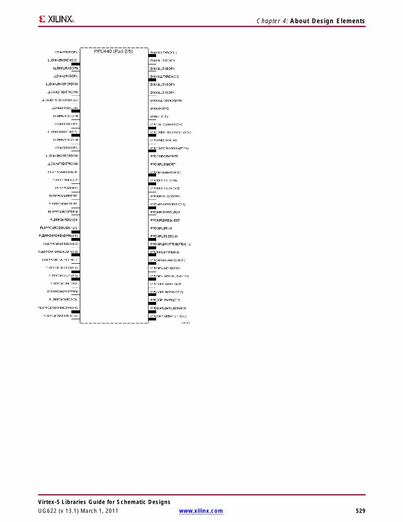
Chapter 4: About Design Elements
Virtex-5 Libraries Guide for Schematic DesignsUG622 (v 13.1) March 1, 2011 www.xilinx.com 529
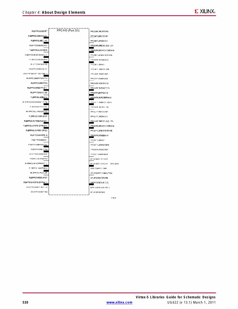
Chapter 4: About Design Elements
Virtex-5 Libraries Guide for Schematic Designs530 www.xilinx.com UG622 (v 13.1) March 1, 2011
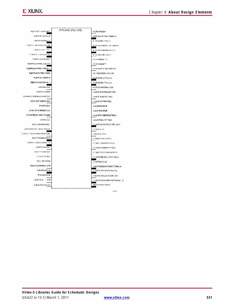
Chapter 4: About Design Elements
Virtex-5 Libraries Guide for Schematic DesignsUG622 (v 13.1) March 1, 2011 www.xilinx.com 531

Chapter 4: About Design Elements
IntroductionThis design element is a dual issue, superscalar processor that provides significant performance improvementover the older PowerPC® 405 while implementing the same instruction set architecture.
Design Entry MethodThis design element can be used in schematics.
For More Information• See the IBM PPC440x5 CPU Core User’s Manual.
• See the Virtex-5 FPGA Data Sheet DC and Switching Characteristics.
• See the Virtex-5 FPGA User Guide.
Virtex-5 Libraries Guide for Schematic Designs532 www.xilinx.com UG622 (v 13.1) March 1, 2011

Chapter 4: About Design Elements
PULLDOWNPrimitive: Resistor to GND for Input Pads, Open-Drain, and 3-State Outputs
IntroductionThis resistor element is connected to input, output, or bidirectional pads to guarantee a logic Low level fornodes that might float.
Port DescriptionsPort Direction Width FunctionO Output 1 Pulldown output (connect directly to top level port)
Design Entry MethodThis design element can be used in schematics.
This element can be connected to a net in the following locations on a top-level schematic file:
• A net connected to an input IO Marker.
• A net connected to both an output IO Marker and 3-statable IO element, such as an OBUFT.
For More Information• See the Virtex-5 FPGA User Guide.
• See the Virtex-5 FPGA Data Sheet DC and Switching Characteristics.
Virtex-5 Libraries Guide for Schematic DesignsUG622 (v 13.1) March 1, 2011 www.xilinx.com 533
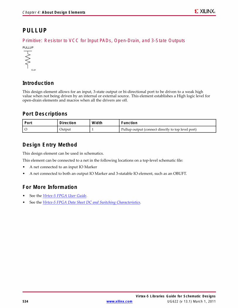
Chapter 4: About Design Elements
PULLUPPrimitive: Resistor to VCC for Input PADs, Open-Drain, and 3-State Outputs
IntroductionThis design element allows for an input, 3-state output or bi-directional port to be driven to a weak highvalue when not being driven by an internal or external source. This element establishes a High logic level foropen-drain elements and macros when all the drivers are off.
Port DescriptionsPort Direction Width FunctionO Output 1 Pullup output (connect directly to top level port)
Design Entry MethodThis design element can be used in schematics.
This element can be connected to a net in the following locations on a top-level schematic file:
• A net connected to an input IO Marker
• A net connected to both an output IO Marker and 3-statable IO element, such as an OBUFT.
For More Information• See the Virtex-5 FPGA User Guide.
• See the Virtex-5 FPGA Data Sheet DC and Switching Characteristics.
Virtex-5 Libraries Guide for Schematic Designs534 www.xilinx.com UG622 (v 13.1) March 1, 2011
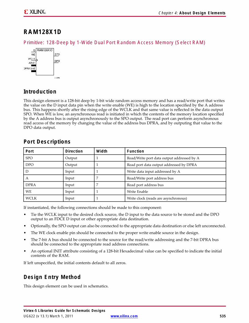
Chapter 4: About Design Elements
RAM128X1DPrimitive: 128-Deep by 1-Wide Dual Port Random Access Memory (Select RAM)
IntroductionThis design element is a 128-bit deep by 1-bit wide random access memory and has a read/write port that writesthe value on the D input data pin when the write enable (WE) is high to the location specified by the A addressbus. This happens shortly after the rising edge of the WCLK and that same value is reflected in the data outputSPO. When WE is low, an asynchronous read is initiated in which the contents of the memory location specifiedby the A address bus is output asynchronously to the SPO output. The read port can perform asynchronousread access of the memory by changing the value of the address bus DPRA, and by outputing that value to theDPO data output.
Port DescriptionsPort Direction Width FunctionSPO Output 1 Read/Write port data output addressed by A
DPO Output 1 Read port data output addressed by DPRA
D Input 1 Write data input addressed by A
A Input 7 Read/Write port address bus
DPRA Input 7 Read port address bus
WE Input 1 Write Enable
WCLK Input 1 Write clock (reads are asynchronous)
If instantiated, the following connections should be made to this component:
• Tie the WCLK input to the desired clock source, the D input to the data source to be stored and the DPOoutput to an FDCE D input or other appropriate data destination.
• Optionally, the SPO output can also be connected to the appropriate data destination or else left unconnected.
• The WE clock enable pin should be connected to the proper write enable source in the design.
• The 7-bit A bus should be connected to the source for the read/write addressing and the 7-bit DPRA busshould be connected to the appropriate read address connections.
• An optional INIT attribute consisting of a 128-bit Hexadecimal value can be specified to indicate the initialcontents of the RAM.
If left unspecified, the initial contents default to all zeros.
Design Entry MethodThis design element can be used in schematics.
Virtex-5 Libraries Guide for Schematic DesignsUG622 (v 13.1) March 1, 2011 www.xilinx.com 535

Chapter 4: About Design Elements
Available AttributesAttribute Type Allowed Values Default DescriptionINIT Hexadecimal Any 128-Bit Value All zeros Specifies the initial contents of the
RAM.
For More Information• See the Virtex-5 FPGA User Guide.
• See the Virtex-5 FPGA Data Sheet DC and Switching Characteristics.
Virtex-5 Libraries Guide for Schematic Designs536 www.xilinx.com UG622 (v 13.1) March 1, 2011

Chapter 4: About Design Elements
RAM16X1DPrimitive: 16-Deep by 1-Wide Static Dual Port Synchronous RAM
IntroductionThis element is a 16-word by 1-bit static dual port random access memory with synchronous write capability.The device has two address ports: the read address (DPRA3:DPRA0) and the write address (A3:A0). These twoaddress ports are asynchronous. The read address controls the location of the data driven out of the output pin(DPO), and the write address controls the destination of a valid write transaction. When the write enable (WE) isLow, transitions on the write clock (WCLK) are ignored and data stored in the RAM is not affected.
When WE is High, any positive transition on (WCLK) loads the data on the data input (D) into the word selectedby the 4-bit write address. For predictable performance, write address and data inputs must be stable before aLow-to-High (WCLK) transition. This RAM block assumes an active-High (WCLK). (WCLK) can be active-Highor active-Low. Any inverter placed on the (WCLK) input net is absorbed into the block.
The SPO output reflects the data in the memory cell addressed by A3:A0. The DPO output reflects the datain the memory cell addressed by DPRA3:DPRA0.
Note The write process is not affected by the address on the read address port.
You can use the INIT attribute to directly specify an initial value. The value must be a hexadecimal number, forexample, INIT=ABAC. If the INIT attribute is not specified, the RAM is initialized with all zeros.
Logic TableMode selection is shown in the following logic table:
Inputs Outputs
WE (mode) WCLK D SPO DPO0 (read) X X data_a data_d
1 (read) 0 X data_a data_d
1 (read) 1 X data_a data_d
1 (write) ↑ D D data_d
1 (read) ↓ X data_a data_d
data_a = word addressed by bits A3-A0
data_d = word addressed by bits DPRA3-DPRA0
Virtex-5 Libraries Guide for Schematic DesignsUG622 (v 13.1) March 1, 2011 www.xilinx.com 537
Chapter 4: About Design Elements
Design Entry MethodThis design element can be used in schematics.
Available AttributesAttribute Type Allowed Values Default DescriptionINIT Hexadecimal Any 16-Bit Value All
zeros.Initializes RAMs, registers, and look-uptables.
For More Information• See the Virtex-5 FPGA User Guide.
• See the Virtex-5 FPGA Data Sheet DC and Switching Characteristics.
Virtex-5 Libraries Guide for Schematic Designs538 www.xilinx.com UG622 (v 13.1) March 1, 2011
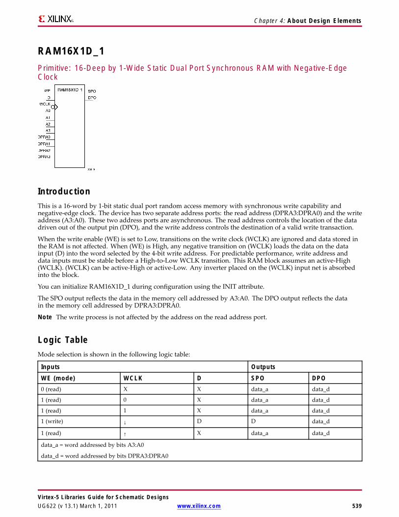
Chapter 4: About Design Elements
RAM16X1D_1Primitive: 16-Deep by 1-Wide Static Dual Port Synchronous RAM with Negative-EdgeClock
IntroductionThis is a 16-word by 1-bit static dual port random access memory with synchronous write capability andnegative-edge clock. The device has two separate address ports: the read address (DPRA3:DPRA0) and the writeaddress (A3:A0). These two address ports are asynchronous. The read address controls the location of the datadriven out of the output pin (DPO), and the write address controls the destination of a valid write transaction.
When the write enable (WE) is set to Low, transitions on the write clock (WCLK) are ignored and data stored inthe RAM is not affected. When (WE) is High, any negative transition on (WCLK) loads the data on the datainput (D) into the word selected by the 4-bit write address. For predictable performance, write address anddata inputs must be stable before a High-to-Low WCLK transition. This RAM block assumes an active-High(WCLK). (WCLK) can be active-High or active-Low. Any inverter placed on the (WCLK) input net is absorbedinto the block.
You can initialize RAM16X1D_1 during configuration using the INIT attribute.
The SPO output reflects the data in the memory cell addressed by A3:A0. The DPO output reflects the datain the memory cell addressed by DPRA3:DPRA0.
Note The write process is not affected by the address on the read address port.
Logic TableMode selection is shown in the following logic table:
Inputs Outputs
WE (mode) WCLK D SPO DPO0 (read) X X data_a data_d
1 (read) 0 X data_a data_d
1 (read) 1 X data_a data_d
1 (write) ↓ D D data_d
1 (read) ↑ X data_a data_d
data_a = word addressed by bits A3:A0
data_d = word addressed by bits DPRA3:DPRA0
Virtex-5 Libraries Guide for Schematic DesignsUG622 (v 13.1) March 1, 2011 www.xilinx.com 539

Chapter 4: About Design Elements
Port DescriptionsPort Direction Width FunctionDPO Output 1 Read-only 1-Bit data output
SPO Output 1 R/W 1-Bit data output
A0 Input 1 R/W address[0] input
A1 Input 1 R/W address[1] input
A2 Input 1 R/W address[2] input
A3 Input 1 R/W address[3] input
D Input 1 Write 1-Bit data input
DPRA0 Input 1 Read-only address[0] input
DPRA1 Input 1 Read-only address[1] input
DPRA2 Input 1 Read-only address[2] input
DPRA3 Input 1 Read-only address[3] input
WCLK Input 1 Write clock input
WE Input 1 Write enable input
Design Entry MethodThis design element can be used in schematics.
Available Attributes
Attribute TypeAllowedValues Default Description
INIT Hexadecimal Any 16-Bit Value All zeros Initializes RAMs, registers, and look-uptables.
For More Information• See the Virtex-5 FPGA User Guide.
• See the Virtex-5 FPGA Data Sheet DC and Switching Characteristics.
Virtex-5 Libraries Guide for Schematic Designs540 www.xilinx.com UG622 (v 13.1) March 1, 2011
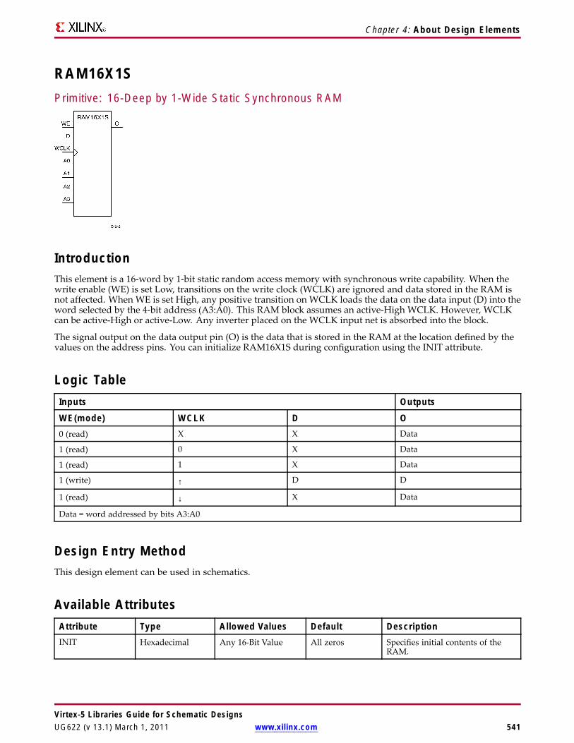
Chapter 4: About Design Elements
RAM16X1SPrimitive: 16-Deep by 1-Wide Static Synchronous RAM
IntroductionThis element is a 16-word by 1-bit static random access memory with synchronous write capability. When thewrite enable (WE) is set Low, transitions on the write clock (WCLK) are ignored and data stored in the RAM isnot affected. When WE is set High, any positive transition on WCLK loads the data on the data input (D) into theword selected by the 4-bit address (A3:A0). This RAM block assumes an active-High WCLK. However, WCLKcan be active-High or active-Low. Any inverter placed on the WCLK input net is absorbed into the block.
The signal output on the data output pin (O) is the data that is stored in the RAM at the location defined by thevalues on the address pins. You can initialize RAM16X1S during configuration using the INIT attribute.
Logic TableInputs Outputs
WE(mode) WCLK D O0 (read) X X Data
1 (read) 0 X Data
1 (read) 1 X Data
1 (write) ↑ D D
1 (read) ↓ X Data
Data = word addressed by bits A3:A0
Design Entry MethodThis design element can be used in schematics.
Available AttributesAttribute Type Allowed Values Default DescriptionINIT Hexadecimal Any 16-Bit Value All zeros Specifies initial contents of the
RAM.
Virtex-5 Libraries Guide for Schematic DesignsUG622 (v 13.1) March 1, 2011 www.xilinx.com 541

Chapter 4: About Design Elements
For More Information• See the Virtex-5 FPGA User Guide.
• See the Virtex-5 FPGA Data Sheet DC and Switching Characteristics.
Virtex-5 Libraries Guide for Schematic Designs542 www.xilinx.com UG622 (v 13.1) March 1, 2011

Chapter 4: About Design Elements
RAM16X1S_1Primitive: 16-Deep by 1-Wide Static Synchronous RAM with Negative-Edge Clock
IntroductionThis element is a 16-word by 1-bit static random access memory with synchronous write capability andnegative-edge clock. When the write enable (WE) is Low, transitions on the write clock (WCLK) are ignoredand data stored in the RAM is not affected. When (WE) is High, any negative transition on (WCLK) loads thedata on the data input (D) into the word selected by the 4-bit address (A3:A0). For predictable performance,address and data inputs must be stable before a High-to-Low WCLK transition. This RAM block assumes anactive-Low (WCLK). However, (WCLK) can be active-High or active-Low. Any inverter placed on the (WCLK)input net is absorbed into the block.
The signal output on the data output pin (O) is the data that is stored in the RAM at the location defined bythe values on the address pins.
You can initialize this element during configuration using the INIT attribute.
Logic TableInputs Outputs
WE(mode) WCLK D O0 (read) X X Data
1 (read) 0 X Data
1 (read) 1 X Data
1 (write) ↓ D D
1 (read) ↑ X Data
Data = word addressed by bits A3:A0
Design Entry MethodThis design element can be used in schematics.
Available AttributesAttribute Type Allowed Values Default DescriptionINIT Hexadecimal Any 16-Bit Value All zeros Specifies initial contents of the
RAM.
Virtex-5 Libraries Guide for Schematic DesignsUG622 (v 13.1) March 1, 2011 www.xilinx.com 543

Chapter 4: About Design Elements
For More Information• See the Virtex-5 FPGA User Guide.
• See the Virtex-5 FPGA Data Sheet DC and Switching Characteristics.
Virtex-5 Libraries Guide for Schematic Designs544 www.xilinx.com UG622 (v 13.1) March 1, 2011
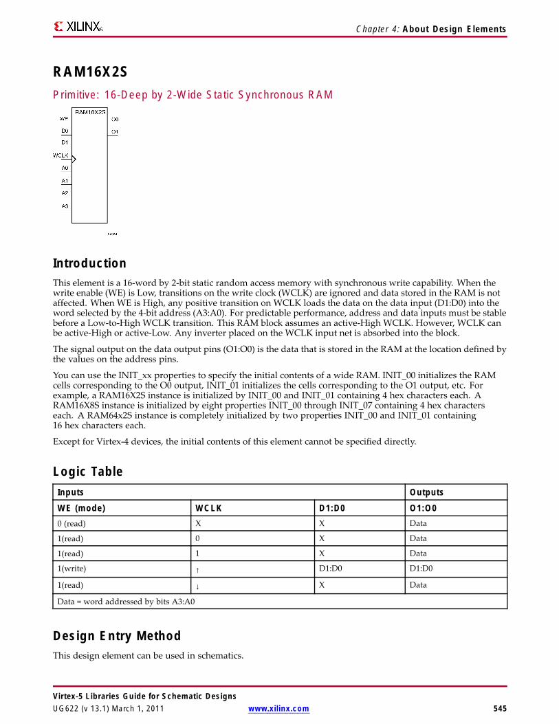
Chapter 4: About Design Elements
RAM16X2SPrimitive: 16-Deep by 2-Wide Static Synchronous RAM
IntroductionThis element is a 16-word by 2-bit static random access memory with synchronous write capability. When thewrite enable (WE) is Low, transitions on the write clock (WCLK) are ignored and data stored in the RAM is notaffected. When WE is High, any positive transition on WCLK loads the data on the data input (D1:D0) into theword selected by the 4-bit address (A3:A0). For predictable performance, address and data inputs must be stablebefore a Low-to-High WCLK transition. This RAM block assumes an active-High WCLK. However, WCLK canbe active-High or active-Low. Any inverter placed on the WCLK input net is absorbed into the block.
The signal output on the data output pins (O1:O0) is the data that is stored in the RAM at the location defined bythe values on the address pins.
You can use the INIT_xx properties to specify the initial contents of a wide RAM. INIT_00 initializes the RAMcells corresponding to the O0 output, INIT_01 initializes the cells corresponding to the O1 output, etc. Forexample, a RAM16X2S instance is initialized by INIT_00 and INIT_01 containing 4 hex characters each. ARAM16X8S instance is initialized by eight properties INIT_00 through INIT_07 containing 4 hex characterseach. A RAM64x2S instance is completely initialized by two properties INIT_00 and INIT_01 containing16 hex characters each.
Except for Virtex-4 devices, the initial contents of this element cannot be specified directly.
Logic TableInputs Outputs
WE (mode) WCLK D1:D0 O1:O00 (read) X X Data
1(read) 0 X Data
1(read) 1 X Data
1(write) ↑ D1:D0 D1:D0
1(read) ↓ X Data
Data = word addressed by bits A3:A0
Design Entry MethodThis design element can be used in schematics.
Virtex-5 Libraries Guide for Schematic DesignsUG622 (v 13.1) March 1, 2011 www.xilinx.com 545

Chapter 4: About Design Elements
Available AttributesAttribute Type Allowed Values Default DescriptionINIT_00 to INIT_01 Hexadecimal Any 16-Bit Value All zeros Initializes RAMs, registers, and
look-up tables.
For More Information• See the Virtex-5 FPGA User Guide.
• See the Virtex-5 FPGA Data Sheet DC and Switching Characteristics.
Virtex-5 Libraries Guide for Schematic Designs546 www.xilinx.com UG622 (v 13.1) March 1, 2011
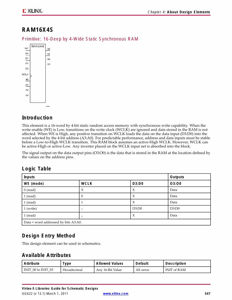
Chapter 4: About Design Elements
RAM16X4SPrimitive: 16-Deep by 4-Wide Static Synchronous RAM
IntroductionThis element is a 16-word by 4-bit static random access memory with synchronous write capability. When thewrite enable (WE) is Low, transitions on the write clock (WCLK) are ignored and data stored in the RAM is notaffected. When WE is High, any positive transition on WCLK loads the data on the data input (D3:D0) into theword selected by the 4-bit address (A3:A0). For predictable performance, address and data inputs must be stablebefore a Low-to-High WCLK transition. This RAM block assumes an active-High WCLK. However, WCLK canbe active-High or active-Low. Any inverter placed on the WCLK input net is absorbed into the block.
The signal output on the data output pins (O3:O0) is the data that is stored in the RAM at the location defined bythe values on the address pins.
Logic TableInputs Outputs
WE (mode) WCLK D3:D0 O3:O00 (read) X X Data
1 (read) 0 X Data
1 (read) 1 X Data
1 (write) ↑ D3:D0 D3:D0
1 (read) ↓ X Data
Data = word addressed by bits A3:A0.
Design Entry MethodThis design element can be used in schematics.
Available AttributesAttribute Type Allowed Values Default DescriptionINIT_00 to INIT_03 Hexadecimal Any 16-Bit Value All zeros INIT of RAM
Virtex-5 Libraries Guide for Schematic DesignsUG622 (v 13.1) March 1, 2011 www.xilinx.com 547

Chapter 4: About Design Elements
For More Information• See the Virtex-5 FPGA User Guide.
• See the Virtex-5 FPGA Data Sheet DC and Switching Characteristics.
Virtex-5 Libraries Guide for Schematic Designs548 www.xilinx.com UG622 (v 13.1) March 1, 2011
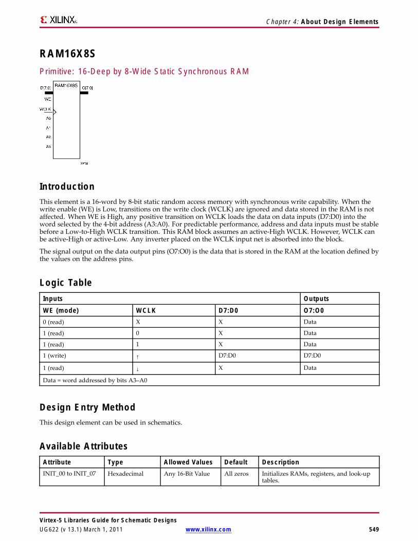
Chapter 4: About Design Elements
RAM16X8SPrimitive: 16-Deep by 8-Wide Static Synchronous RAM
IntroductionThis element is a 16-word by 8-bit static random access memory with synchronous write capability. When thewrite enable (WE) is Low, transitions on the write clock (WCLK) are ignored and data stored in the RAM is notaffected. When WE is High, any positive transition on WCLK loads the data on data inputs (D7:D0) into theword selected by the 4-bit address (A3:A0). For predictable performance, address and data inputs must be stablebefore a Low-to-High WCLK transition. This RAM block assumes an active-High WCLK. However, WCLK canbe active-High or active-Low. Any inverter placed on the WCLK input net is absorbed into the block.
The signal output on the data output pins (O7:O0) is the data that is stored in the RAM at the location defined bythe values on the address pins.
Logic TableInputs Outputs
WE (mode) WCLK D7:D0 O7:O00 (read) X X Data
1 (read) 0 X Data
1 (read) 1 X Data
1 (write) ↑ D7:D0 D7:D0
1 (read) ↓ X Data
Data = word addressed by bits A3–A0
Design Entry MethodThis design element can be used in schematics.
Available AttributesAttribute Type Allowed Values Default DescriptionINIT_00 to INIT_07 Hexadecimal Any 16-Bit Value All zeros Initializes RAMs, registers, and look-up
tables.
Virtex-5 Libraries Guide for Schematic DesignsUG622 (v 13.1) March 1, 2011 www.xilinx.com 549

Chapter 4: About Design Elements
For More Information• See the Virtex-5 FPGA User Guide.
• See the Virtex-5 FPGA Data Sheet DC and Switching Characteristics.
Virtex-5 Libraries Guide for Schematic Designs550 www.xilinx.com UG622 (v 13.1) March 1, 2011
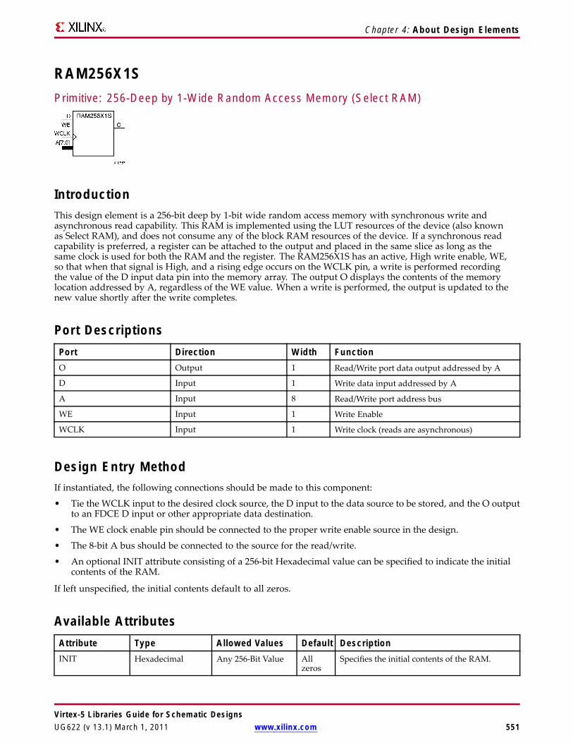
Chapter 4: About Design Elements
RAM256X1SPrimitive: 256-Deep by 1-Wide Random Access Memory (Select RAM)
IntroductionThis design element is a 256-bit deep by 1-bit wide random access memory with synchronous write andasynchronous read capability. This RAM is implemented using the LUT resources of the device (also knownas Select RAM), and does not consume any of the block RAM resources of the device. If a synchronous readcapability is preferred, a register can be attached to the output and placed in the same slice as long as thesame clock is used for both the RAM and the register. The RAM256X1S has an active, High write enable, WE,so that when that signal is High, and a rising edge occurs on the WCLK pin, a write is performed recordingthe value of the D input data pin into the memory array. The output O displays the contents of the memorylocation addressed by A, regardless of the WE value. When a write is performed, the output is updated to thenew value shortly after the write completes.
Port DescriptionsPort Direction Width FunctionO Output 1 Read/Write port data output addressed by A
D Input 1 Write data input addressed by A
A Input 8 Read/Write port address bus
WE Input 1 Write Enable
WCLK Input 1 Write clock (reads are asynchronous)
Design Entry MethodIf instantiated, the following connections should be made to this component:
• Tie the WCLK input to the desired clock source, the D input to the data source to be stored, and the O outputto an FDCE D input or other appropriate data destination.
• The WE clock enable pin should be connected to the proper write enable source in the design.
• The 8-bit A bus should be connected to the source for the read/write.
• An optional INIT attribute consisting of a 256-bit Hexadecimal value can be specified to indicate the initialcontents of the RAM.
If left unspecified, the initial contents default to all zeros.
Available AttributesAttribute Type Allowed Values Default DescriptionINIT Hexadecimal Any 256-Bit Value All
zerosSpecifies the initial contents of the RAM.
Virtex-5 Libraries Guide for Schematic DesignsUG622 (v 13.1) March 1, 2011 www.xilinx.com 551

Chapter 4: About Design Elements
For More Information• See the Virtex-5 FPGA User Guide.
• See the Virtex-5 FPGA Data Sheet DC and Switching Characteristics.
Virtex-5 Libraries Guide for Schematic Designs552 www.xilinx.com UG622 (v 13.1) March 1, 2011

Chapter 4: About Design Elements
RAM32MPrimitive: 32-Deep by 8-bit Wide Multi Port Random Access Memory (Select RAM)
IntroductionThis design element is a 32-bit deep by 8-bit wide, multi-port, random access memory with synchronous writeand asynchronous independent, 2-bit, wide-read capability. This RAM is implemented using the LUT resourcesof the device known as SelectRAM™, and does not consume any of the Block RAM resources of the device. TheRAM32M is implemented in a single slice and consists of one 8-bit write, 2-bit read port and three separate 2-bitread ports from the same memory. This configuration allows for byte-wide write and independent 2-bit readaccess RAM. If the DIA, DIB, DIC and DID inputs are all tied to the same data inputs, the RAM can becomea 1 read/write port, 3 independent read port, 32x2 quad port memory. If DID is grounded, DOD is not used,while ADDRA, ADDRB and ADDRC are tied to the same address, the RAM becomes a 32x6 simple dual portRAM. If ADDRD is tied to ADDRA, ADDRB, and ADDRC, then the RAM is a 32x8 single port RAM. There areseveral other possible configurations for this RAM.
Virtex-5 Libraries Guide for Schematic DesignsUG622 (v 13.1) March 1, 2011 www.xilinx.com 553

Chapter 4: About Design Elements
Port DescriptionsPort Direction Width FunctionDOA Output 2 Read port data outputs addressed by ADDRA
DOB Output 2 Read port data outputs addressed by ADDRB
DOC Output 2 Read port data outputs addressed by ADDRC
DOD Output 2 Read/Write port data outputs addressed by ADDRD
DIA Input 2 Write data inputs addressed by ADDRD (read output isaddressed by ADDRA)
DIB Input 2 Write data inputs addressed by ADDRD (read output isaddressed by ADDRB)
DIC Input 2 Write data inputs addressed by ADDRD (read output isaddressed by ADDRC)
DID Input 2 Write data inputs addressed by ADDRD
ADDRA Input 5 Read address bus A
ADDRB Input 5 Read address bus B
ADDRC Input 5 Read address bus C
ADDRD Input 5 8-bit data write port, 2-bit data read port address bus D
WE Input 1 Write Enable
WCLK Input 1 Write clock (reads are asynchronous)
Design Entry MethodThis design element can be used in schematics.
This element can be inferred by some synthesis tools by describing a RAM with a synchronous write andasynchronous read capability. Consult your synthesis tool documentation for details on RAM inferencecapabilities and coding examples. Xilinx suggests that you instantiate RAM32Ms if you have a need to implicitlyspecify the RAM function, or if you need to manually place or relationally place the component. If a synchronousread capability is desired, the RAM32M outputs can be connected to an FDRSE (FDCPE is asynchronous set/resetis necessary) in order to improve the output timing of the function. However, this is not necessary for theproper operation of the RAM.
If you want to have the data clocked on the negative edge of a clock, an inverter can be described on the clockinput to this component. This inverter will be absorbed into the block, giving you the ability to write to the RAMon falling clock edges.
If instantiated, the following connections should be made to this component. Tie the WCLK input to the desiredclock source, the DIA, DIB, DIC and DID inputs to the data source to be stored and the DOA, DOB, DOC andDOD outputs to an FDCE D input or other appropriate data destination or left unconnected if not used. The WEclock enable pin should be connected to the proper write enable source in the design. The 5-bit ADDRD busshould be connected to the source for the read/write addressing and the 5-bit ADDRA, ADDRB and ADDRCbuses should be connected to the appropriate read address connections. The optional INIT_A, INIT_B, INIT_Cand INIT_D attributes consisting of a 64-bit hexadecimal values that specifies each port’s initial memory contentscan be specified. The INIT value correlates to the RAM addressing by the following equation: ADDRy[z] =INIT_y[2*z+1:2*z]. For instance, if the RAM ADDRC port is addressed to 00001, then the INIT_C[3:2] valueswould be the initial values shown on the DOC port before the first write occurs at that address. If left unspecified,the initial contents will default to all zeros.
Virtex-5 Libraries Guide for Schematic Designs554 www.xilinx.com UG622 (v 13.1) March 1, 2011
Chapter 4: About Design Elements
Available AttributesAttribute Type Allowed Values Default DescriptionINIT_A Hexadecimal Any 64-Bit Value All zeros Specifies the initial contents of the RAM on
the A port.
INIT_B Hexadecimal Any 64-Bit Value All zeros Specifies the initial contents of the RAM onthe B port.
INIT_C Hexadecimal Any 64-Bit Value All zeros Specifies the initial contents of the RAM onthe C port.
INIT_D Hexadecimal Any 64-Bit Value All zeros Specifies the initial contents of the RAM onthe D port.
For More Information• See the Virtex-5 FPGA User Guide.
• See the Virtex-5 FPGA Data Sheet DC and Switching Characteristics.
Virtex-5 Libraries Guide for Schematic DesignsUG622 (v 13.1) March 1, 2011 www.xilinx.com 555
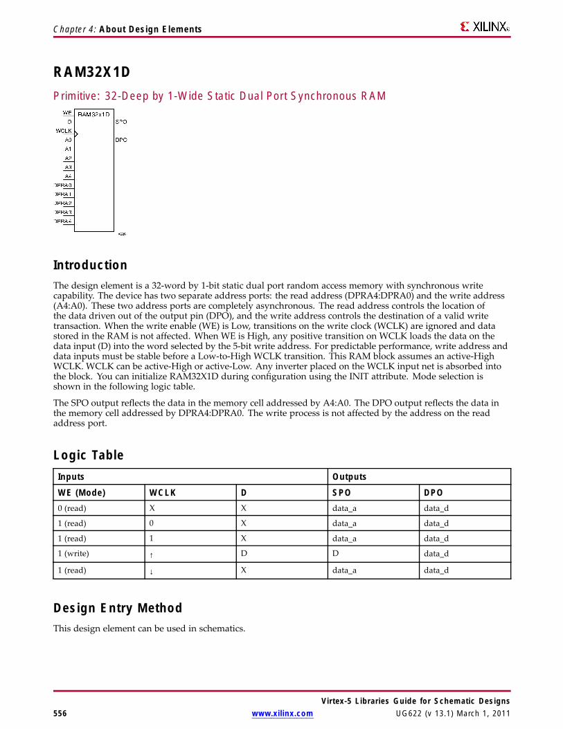
Chapter 4: About Design Elements
RAM32X1DPrimitive: 32-Deep by 1-Wide Static Dual Port Synchronous RAM
IntroductionThe design element is a 32-word by 1-bit static dual port random access memory with synchronous writecapability. The device has two separate address ports: the read address (DPRA4:DPRA0) and the write address(A4:A0). These two address ports are completely asynchronous. The read address controls the location ofthe data driven out of the output pin (DPO), and the write address controls the destination of a valid writetransaction. When the write enable (WE) is Low, transitions on the write clock (WCLK) are ignored and datastored in the RAM is not affected. When WE is High, any positive transition on WCLK loads the data on thedata input (D) into the word selected by the 5-bit write address. For predictable performance, write address anddata inputs must be stable before a Low-to-High WCLK transition. This RAM block assumes an active-HighWCLK. WCLK can be active-High or active-Low. Any inverter placed on the WCLK input net is absorbed intothe block. You can initialize RAM32X1D during configuration using the INIT attribute. Mode selection isshown in the following logic table.
The SPO output reflects the data in the memory cell addressed by A4:A0. The DPO output reflects the data inthe memory cell addressed by DPRA4:DPRA0. The write process is not affected by the address on the readaddress port.
Logic TableInputs Outputs
WE (Mode) WCLK D SPO DPO0 (read) X X data_a data_d
1 (read) 0 X data_a data_d
1 (read) 1 X data_a data_d
1 (write) ↑ D D data_d
1 (read) ↓ X data_a data_d
Design Entry MethodThis design element can be used in schematics.
Virtex-5 Libraries Guide for Schematic Designs556 www.xilinx.com UG622 (v 13.1) March 1, 2011

Chapter 4: About Design Elements
Available Attributes
Attribute TypeAllowedValues Default Descriptions
INIT Hexadecimal Any 32-BitValue
All Zeros Initializes ROMs, RAMs, registers, and look-uptables.
For More Information• See the Virtex-5 FPGA User Guide.
• See the Virtex-5 FPGA Data Sheet DC and Switching Characteristics.
Virtex-5 Libraries Guide for Schematic DesignsUG622 (v 13.1) March 1, 2011 www.xilinx.com 557

Chapter 4: About Design Elements
RAM32X1SPrimitive: 32-Deep by 1-Wide Static Synchronous RAM
IntroductionThe design element is a 32-word by 1-bit static random access memory with synchronous write capability. Whenthe write enable is Low, transitions on the write clock (WCLK) are ignored and data stored in the RAM is notaffected. When (WE) is High, any positive transition on (WCLK) loads the data on the data input (D) into theword selected by the 5-bit address (A4-A0). For predictable performance, address and data inputs must be stablebefore a Low-to-High (WCLK) transition. This RAM block assumes an active-High (WCLK). However, (WCLK)can be active-High or active-Low. Any inverter placed on the (WCLK) input net is absorbed into the block.
The signal output on the data output pin (O) is the data that is stored in the RAM at the location defined by thevalues on the address pins. You can initialize RAM32X1S during configuration using the INIT attribute.
Logic TableInputs Outputs
WE (Mode) WCLK D O0 (read) X X Data
1 (read) 0 X Data
1 (read) 1 X Data
1 (write) ↓ D D
1 (read) ↑ X Data
Design Entry MethodThis design element can be used in schematics.
Available AttributesAttribute Type Allowed Values Default DescriptionsINIT Hexadecimal Any 32-Bit Value All zeros Specifies initial contents of the RAM.
For More Information• See the Virtex-5 FPGA User Guide.• See the Virtex-5 FPGA Data Sheet DC and Switching Characteristics.
Virtex-5 Libraries Guide for Schematic Designs558 www.xilinx.com UG622 (v 13.1) March 1, 2011
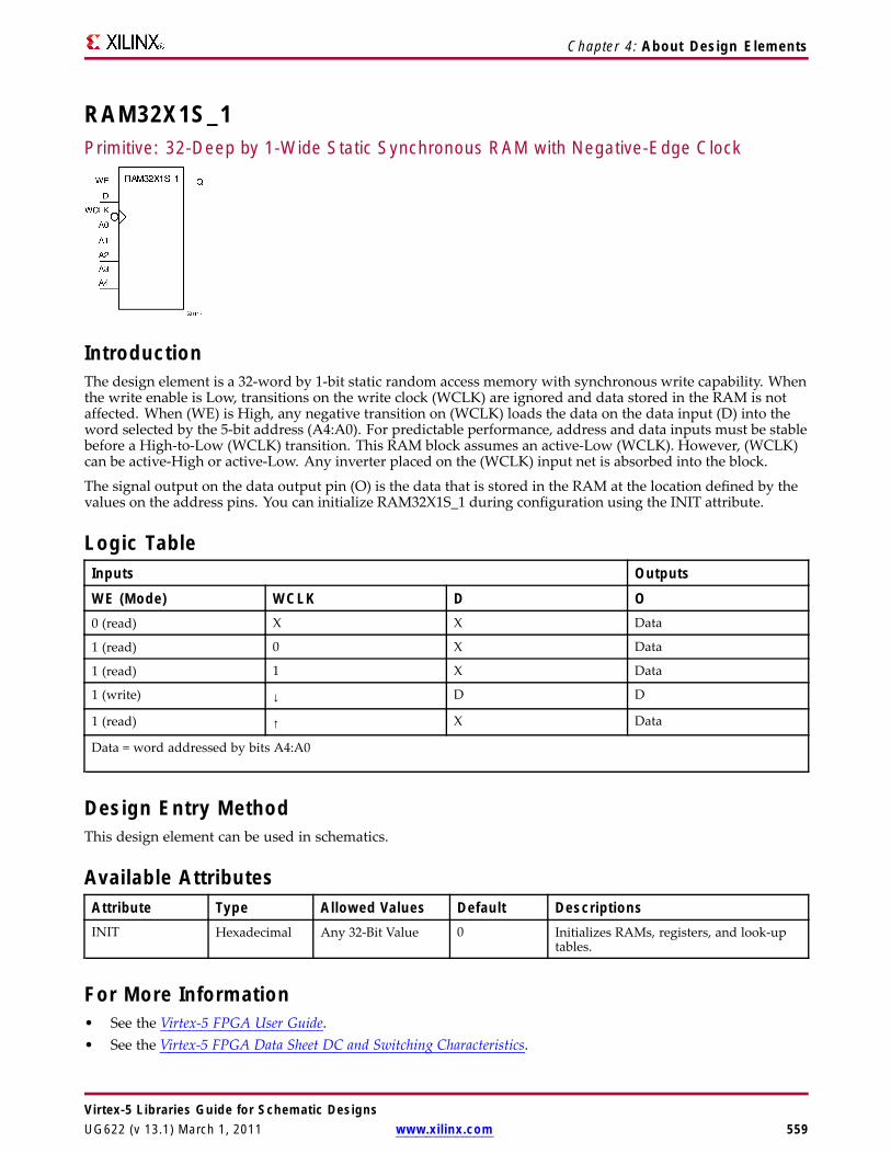
Chapter 4: About Design Elements
RAM32X1S_1Primitive: 32-Deep by 1-Wide Static Synchronous RAM with Negative-Edge Clock
IntroductionThe design element is a 32-word by 1-bit static random access memory with synchronous write capability. Whenthe write enable is Low, transitions on the write clock (WCLK) are ignored and data stored in the RAM is notaffected. When (WE) is High, any negative transition on (WCLK) loads the data on the data input (D) into theword selected by the 5-bit address (A4:A0). For predictable performance, address and data inputs must be stablebefore a High-to-Low (WCLK) transition. This RAM block assumes an active-Low (WCLK). However, (WCLK)can be active-High or active-Low. Any inverter placed on the (WCLK) input net is absorbed into the block.
The signal output on the data output pin (O) is the data that is stored in the RAM at the location defined by thevalues on the address pins. You can initialize RAM32X1S_1 during configuration using the INIT attribute.
Logic TableInputs Outputs
WE (Mode) WCLK D O0 (read) X X Data
1 (read) 0 X Data
1 (read) 1 X Data
1 (write) ↓ D D
1 (read) ↑ X Data
Data = word addressed by bits A4:A0
Design Entry MethodThis design element can be used in schematics.
Available AttributesAttribute Type Allowed Values Default DescriptionsINIT Hexadecimal Any 32-Bit Value 0 Initializes RAMs, registers, and look-up
tables.
For More Information• See the Virtex-5 FPGA User Guide.• See the Virtex-5 FPGA Data Sheet DC and Switching Characteristics.
Virtex-5 Libraries Guide for Schematic DesignsUG622 (v 13.1) March 1, 2011 www.xilinx.com 559

Chapter 4: About Design Elements
RAM32X2SPrimitive: 32-Deep by 2-Wide Static Synchronous RAM
IntroductionThe design element is a 32-word by 2-bit static random access memory with synchronous write capability. Whenthe write enable (WE) is Low, transitions on the write clock (WCLK) are ignored and data stored in the RAM isnot affected. When (WE) is High, any positive transition on (WCLK) loads the data on the data input (D1-D0)into the word selected by the 5-bit address (A4-A0). For predictable performance, address and data inputs mustbe stable before a Low-to-High (WCLK) transition. This RAM block assumes an active-High (WCLK). However,(WCLK) can be active-High or active-Low. Any inverter placed on the (WCLK) input net is absorbed into theblock. The signal output on the data output pins (O1-O0) is the data that is stored in the RAM at the locationdefined by the values on the address pins.
You can use the INIT_00 and INIT_01 properties to specify the initial contents of RAM32X2S.
Logic TableInputs Outputs
WE (Mode) WCLK D O0-O10 (read) X X Data
1 (read) 0 X Data
1 (read) 1 X Data
1 (write) ↑ D1:D0 D1:D0
1 (read) ↓ X Data
Data = word addressed by bits A4:A0
Design Entry MethodThis design element can be used in schematics.
Available AttributesAttribute Type Allowed Values Default DescriptionsINIT_00 Hexadecimal Any 32-Bit Value All zeros INIT for bit 0 of RAM.
INIT_01 Hexadecimal Any 32-Bit Value All zeros INIT for bit 1 of RAM.
Virtex-5 Libraries Guide for Schematic Designs560 www.xilinx.com UG622 (v 13.1) March 1, 2011

Chapter 4: About Design Elements
For More Information• See the Virtex-5 FPGA User Guide.
• See the Virtex-5 FPGA Data Sheet DC and Switching Characteristics.
Virtex-5 Libraries Guide for Schematic DesignsUG622 (v 13.1) March 1, 2011 www.xilinx.com 561
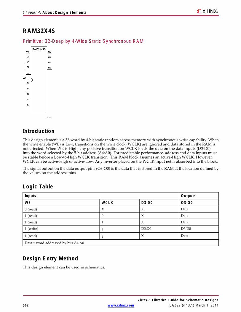
Chapter 4: About Design Elements
RAM32X4SPrimitive: 32-Deep by 4-Wide Static Synchronous RAM
IntroductionThis design element is a 32-word by 4-bit static random access memory with synchronous write capability. Whenthe write enable (WE) is Low, transitions on the write clock (WCLK) are ignored and data stored in the RAM isnot affected. When WE is High, any positive transition on WCLK loads the data on the data inputs (D3-D0)into the word selected by the 5-bit address (A4:A0). For predictable performance, address and data inputs mustbe stable before a Low-to-High WCLK transition. This RAM block assumes an active-High WCLK. However,WCLK can be active-High or active-Low. Any inverter placed on the WCLK input net is absorbed into the block.
The signal output on the data output pins (O3-O0) is the data that is stored in the RAM at the location defined bythe values on the address pins.
Logic TableInputs Outputs
WE WCLK D3-D0 O3-O00 (read) X X Data
1 (read) 0 X Data
1 (read) 1 X Data
1 (write) ↑ D3:D0 D3:D0
1 (read) ↓ X Data
Data = word addressed by bits A4:A0
Design Entry MethodThis design element can be used in schematics.
Virtex-5 Libraries Guide for Schematic Designs562 www.xilinx.com UG622 (v 13.1) March 1, 2011
Chapter 4: About Design Elements
Available AttributesAttribute Type Allowed Values Default DescriptionINIT_00 Hexadecimal Any 32-Bit Value All zeros INIT for bit 0 of RAM.
INIT_01 Hexadecimal Any 32-Bit Value All zeros INIT for bit 1 of RAM.
INIT_02 Hexadecimal Any 32-Bit Value All zeros INIT for bit 2 of RAM.
INIT_03 Hexadecimal Any 32-Bit Value All zeros INIT for bit 3 of RAM.
For More Information• See the Virtex-5 FPGA User Guide.
• See the Virtex-5 FPGA Data Sheet DC and Switching Characteristics.
Virtex-5 Libraries Guide for Schematic DesignsUG622 (v 13.1) March 1, 2011 www.xilinx.com 563

Chapter 4: About Design Elements
RAM32X8SPrimitive: 32-Deep by 8-Wide Static Synchronous RAM
IntroductionThis design element is a 32-word by 8-bit static random access memory with synchronous write capability. Whenthe write enable (WE) is Low, transitions on the write clock (WCLK) are ignored and data stored in the RAM isnot affected. When WE is High, any positive transition on WCLK loads the data on the data inputs (D7:D0)into the word selected by the 5-bit address (A4:A0). For predictable performance, address and data inputs mustbe stable before a Low-to-High WCLK transition. This RAM block assumes an active-High WCLK. However,WCLK can be active-High or active-Low. Any inverter placed on the WCLK input net is absorbed into the block.
The signal output on the data output pins (O7:O0) is the data that is stored in the RAM at the location defined bythe values on the address pins.
Logic TableInputs Outputs
WE (mode) WCLK D7:D0 O7:O00 (read) X X Data
1 (read) 0 X Data
1 (read) 1 X Data
1 (write) ↑ D7:D0 D7:D0
1 (read) ↓ X Data
Data = word addressed by bits A4:A0
Design Entry MethodThis design element can be used in schematics.
Virtex-5 Libraries Guide for Schematic Designs564 www.xilinx.com UG622 (v 13.1) March 1, 2011

Chapter 4: About Design Elements
Available AttributesAttribute Type Allowed Values Default DescriptionINIT_00 Hexadecimal Any 32-Bit Value All zeros INIT for bit 0 of RAM.
INIT_01 Hexadecimal Any 32-Bit Value All zeros INIT for bit 1 of RAM.
INIT_02 Hexadecimal Any 32-Bit Value All zeros INIT for bit 2 of RAM.
INIT_03 Hexadecimal Any 32-Bit Value All zeros INIT for bit 3 of RAM.
INIT_04 Hexadecimal Any 32-Bit Value All zeros INIT for bit 4 of RAM.
INIT_05 Hexadecimal Any 32-Bit Value All zeros INIT for bit 5 of RAM.
INIT_06 Hexadecimal Any 32-Bit Value All zeros INIT for bit 6 of RAM.
INIT_07 Hexadecimal Any 32-Bit Value All zeros INIT for bit 7 of RAM.
For More Information• See the Virtex-5 FPGA User Guide.
• See the Virtex-5 FPGA Data Sheet DC and Switching Characteristics.
Virtex-5 Libraries Guide for Schematic DesignsUG622 (v 13.1) March 1, 2011 www.xilinx.com 565
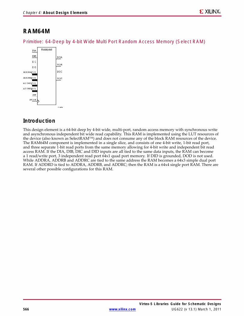
Chapter 4: About Design Elements
RAM64MPrimitive: 64-Deep by 4-bit Wide Multi Port Random Access Memory (Select RAM)
IntroductionThis design element is a 64-bit deep by 4-bit wide, multi-port, random access memory with synchronous writeand asynchronous independent bit wide read capability. This RAM is implemented using the LUT resources ofthe device (also known as SelectRAM™) and does not consume any of the block RAM resources of the device.The RAM64M component is implemented in a single slice, and consists of one 4-bit write, 1-bit read port,and three separate 1-bit read ports from the same memory allowing for 4-bit write and independent bit readaccess RAM. If the DIA, DIB, DIC and DID inputs are all tied to the same data inputs, the RAM can becomea 1 read/write port, 3 independent read port 64x1 quad port memory. If DID is grounded, DOD is not used.While ADDRA, ADDRB and ADDRC are tied to the same address the RAM becomes a 64x3 simple dual portRAM. If ADDRD is tied to ADDRA, ADDRB, and ADDRC; then the RAM is a 64x4 single port RAM. There areseveral other possible configurations for this RAM.
Virtex-5 Libraries Guide for Schematic Designs566 www.xilinx.com UG622 (v 13.1) March 1, 2011
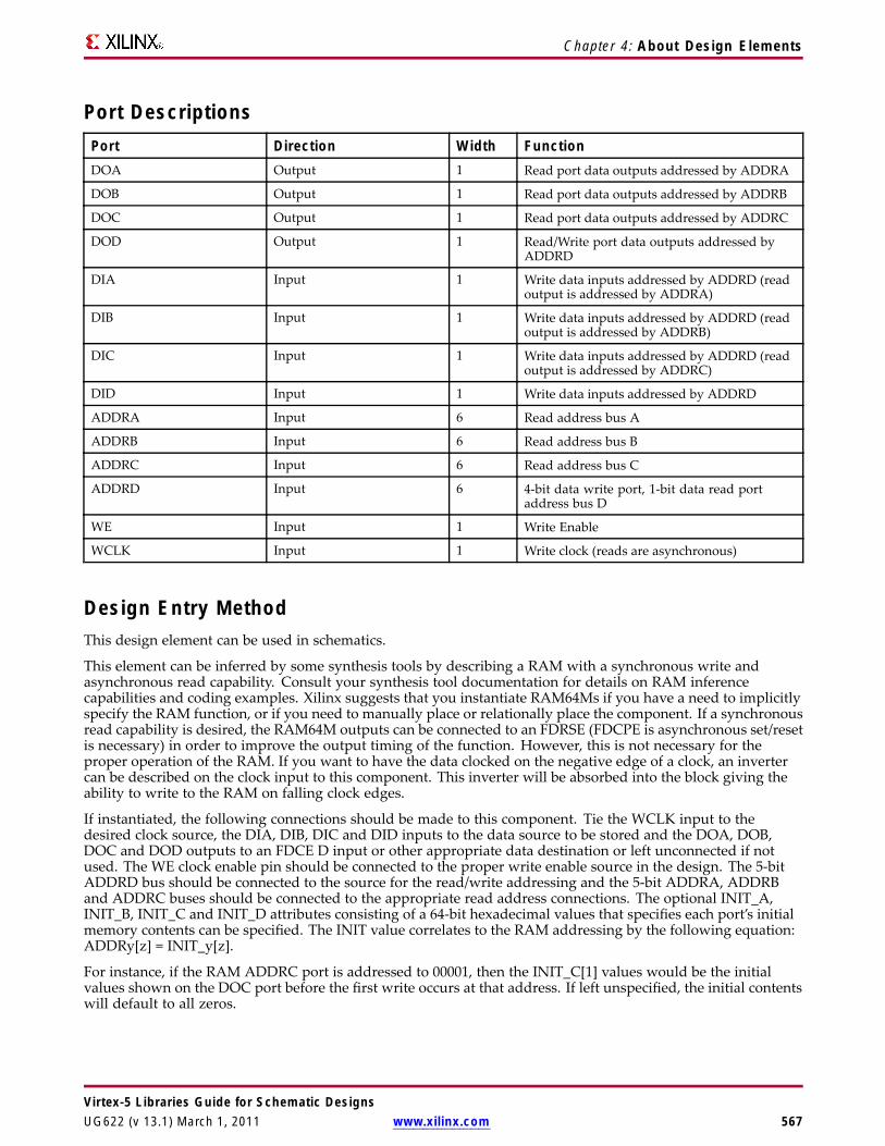
Chapter 4: About Design Elements
Port DescriptionsPort Direction Width FunctionDOA Output 1 Read port data outputs addressed by ADDRA
DOB Output 1 Read port data outputs addressed by ADDRB
DOC Output 1 Read port data outputs addressed by ADDRC
DOD Output 1 Read/Write port data outputs addressed byADDRD
DIA Input 1 Write data inputs addressed by ADDRD (readoutput is addressed by ADDRA)
DIB Input 1 Write data inputs addressed by ADDRD (readoutput is addressed by ADDRB)
DIC Input 1 Write data inputs addressed by ADDRD (readoutput is addressed by ADDRC)
DID Input 1 Write data inputs addressed by ADDRD
ADDRA Input 6 Read address bus A
ADDRB Input 6 Read address bus B
ADDRC Input 6 Read address bus C
ADDRD Input 6 4-bit data write port, 1-bit data read portaddress bus D
WE Input 1 Write Enable
WCLK Input 1 Write clock (reads are asynchronous)
Design Entry MethodThis design element can be used in schematics.
This element can be inferred by some synthesis tools by describing a RAM with a synchronous write andasynchronous read capability. Consult your synthesis tool documentation for details on RAM inferencecapabilities and coding examples. Xilinx suggests that you instantiate RAM64Ms if you have a need to implicitlyspecify the RAM function, or if you need to manually place or relationally place the component. If a synchronousread capability is desired, the RAM64M outputs can be connected to an FDRSE (FDCPE is asynchronous set/resetis necessary) in order to improve the output timing of the function. However, this is not necessary for theproper operation of the RAM. If you want to have the data clocked on the negative edge of a clock, an invertercan be described on the clock input to this component. This inverter will be absorbed into the block giving theability to write to the RAM on falling clock edges.
If instantiated, the following connections should be made to this component. Tie the WCLK input to thedesired clock source, the DIA, DIB, DIC and DID inputs to the data source to be stored and the DOA, DOB,DOC and DOD outputs to an FDCE D input or other appropriate data destination or left unconnected if notused. The WE clock enable pin should be connected to the proper write enable source in the design. The 5-bitADDRD bus should be connected to the source for the read/write addressing and the 5-bit ADDRA, ADDRBand ADDRC buses should be connected to the appropriate read address connections. The optional INIT_A,INIT_B, INIT_C and INIT_D attributes consisting of a 64-bit hexadecimal values that specifies each port’s initialmemory contents can be specified. The INIT value correlates to the RAM addressing by the following equation:ADDRy[z] = INIT_y[z].
For instance, if the RAM ADDRC port is addressed to 00001, then the INIT_C[1] values would be the initialvalues shown on the DOC port before the first write occurs at that address. If left unspecified, the initial contentswill default to all zeros.
Virtex-5 Libraries Guide for Schematic DesignsUG622 (v 13.1) March 1, 2011 www.xilinx.com 567

Chapter 4: About Design Elements
Available AttributesAttribute Type Allowed Values Default DescriptionINIT_A Hexadecimal Any 64-Bit Value All zero Specifies the initial contents of the RAM on
the A port.
INIT_B Hexadecimal Any 64-Bit Value All zero Specifies the initial contents of the RAM onthe B port.
INIT_C Hexadecimal Any 64-Bit Value All zero Specifies the initial contents of the RAM onthe C port.
INIT_D Hexadecimal Any 64-Bit Value All zero Specifies the initial contents of the RAM onthe D port.
For More Information• See the Virtex-5 FPGA User Guide.
• See the Virtex-5 FPGA Data Sheet DC and Switching Characteristics.
Virtex-5 Libraries Guide for Schematic Designs568 www.xilinx.com UG622 (v 13.1) March 1, 2011

Chapter 4: About Design Elements
RAM64X1DPrimitive: 64-Deep by 1-Wide Dual Port Static Synchronous RAM
IntroductionThis design element is a 64-word by 1-bit static dual port random access memory with synchronous writecapability. The device has two separate address ports: the read address (DPRA5:DPRA0) and the write address(A5:A0). These two address ports are completely asynchronous. The read address controls the location ofthe data driven out of the output pin (DPO), and the write address controls the destination of a valid writetransaction. When the write enable (WE) is Low, transitions on the write clock (WCLK) are ignored and datastored in the RAM is not affected.
When WE is High, any positive transition on WCLK loads the data on the data input (D) into the word selectedby the 6-bit (A0:A5) write address. For predictable performance, write address and data inputs must be stablebefore a Low-to-High WCLK transition. This RAM block assumes an active-High WCLK. WCLK can beactive-High or active-Low. Any inverter placed on the WCLK input net is absorbed into the block.
The SPO output reflects the data in the memory cell addressed by A5:A0. The DPO output reflects the datain the memory cell addressed by DPRA5:DPRA0.
Note The write process is not affected by the address on the read address port.
Logic TableInputs Outputs
WE (mode) WCLK D SPO DPO0 (read) X X data_a data_d
1 (read) 0 X data_a data_d
1 (read) 1 X data_a data_d
1 (write) ↑ D D data_d
1 (read) ↓ X data_a data_d
data_a = word addressed by bits A5:A0
data_d = word addressed by bits DPRA5:DPRA0
Design Entry MethodThis design element can be used in schematics.
Virtex-5 Libraries Guide for Schematic DesignsUG622 (v 13.1) March 1, 2011 www.xilinx.com 569
Chapter 4: About Design Elements
Available Attributes
Attribute TypeAllowedValues Default Description
INIT Hexadecimal Any 64-BitValue
All zeros Initializes RAMs, registers, and look-up tables.
For More Information• See the Virtex-5 FPGA User Guide.
• See the Virtex-5 FPGA Data Sheet DC and Switching Characteristics.
Virtex-5 Libraries Guide for Schematic Designs570 www.xilinx.com UG622 (v 13.1) March 1, 2011
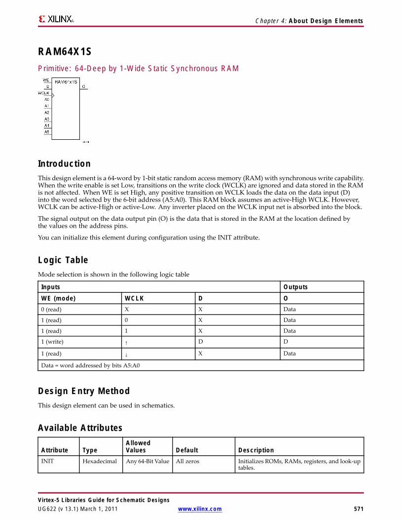
Chapter 4: About Design Elements
RAM64X1SPrimitive: 64-Deep by 1-Wide Static Synchronous RAM
IntroductionThis design element is a 64-word by 1-bit static random access memory (RAM) with synchronous write capability.When the write enable is set Low, transitions on the write clock (WCLK) are ignored and data stored in the RAMis not affected. When WE is set High, any positive transition on WCLK loads the data on the data input (D)into the word selected by the 6-bit address (A5:A0). This RAM block assumes an active-High WCLK. However,WCLK can be active-High or active-Low. Any inverter placed on the WCLK input net is absorbed into the block.
The signal output on the data output pin (O) is the data that is stored in the RAM at the location defined bythe values on the address pins.
You can initialize this element during configuration using the INIT attribute.
Logic TableMode selection is shown in the following logic table
Inputs Outputs
WE (mode) WCLK D O0 (read) X X Data
1 (read) 0 X Data
1 (read) 1 X Data
1 (write) ↑ D D
1 (read) ↓ X Data
Data = word addressed by bits A5:A0
Design Entry MethodThis design element can be used in schematics.
Available Attributes
Attribute TypeAllowedValues Default Description
INIT Hexadecimal Any 64-Bit Value All zeros Initializes ROMs, RAMs, registers, and look-uptables.
Virtex-5 Libraries Guide for Schematic DesignsUG622 (v 13.1) March 1, 2011 www.xilinx.com 571

Chapter 4: About Design Elements
For More Information• See the Virtex-5 FPGA User Guide.
• See the Virtex-5 FPGA Data Sheet DC and Switching Characteristics.
Virtex-5 Libraries Guide for Schematic Designs572 www.xilinx.com UG622 (v 13.1) March 1, 2011

Chapter 4: About Design Elements
RAM64X1S_1Primitive: 64-Deep by 1-Wide Static Synchronous RAM with Negative-Edge Clock
IntroductionThis design element is a 64-word by 1-bit static random access memory with synchronous write capability. Whenthe write enable is Low, transitions on the write clock (WCLK) are ignored and data stored in the RAM is notaffected. When (WE) is High, any negative transition on (WCLK) loads the data on the data input (D) into theword selected by the 6-bit address (A5:A0). For predictable performance, address and data inputs must be stablebefore a High-to-Low (WCLK) transition. This RAM block assumes an active-Low (WCLK). However, (WCLK)can be active-High or active-Low. Any inverter placed on the (WCLK) input net is absorbed into the block.
The signal output on the data output pin (O) is the data that is stored in the RAM at the location defined bythe values on the address pins.
You can initialize this element during configuration using the INIT attribute.
Logic TableInputs Outputs
WE (mode) WCLK D O0 (read) X X Data
1 (read) 0 X Data
1 (read) 1 X Data
1 (write) ↓ D D
1 (read) ↑ X Data
Data = word addressed by bits A5:A0
Design Entry MethodThis design element can be used in schematics.
Available AttributesAttribute Type Allowed Values Default DescriptionINIT Hexadecimal Any 64-Bit Value All zeros Initializes ROMs, RAMs, registers, and look-up
tables.
Virtex-5 Libraries Guide for Schematic DesignsUG622 (v 13.1) March 1, 2011 www.xilinx.com 573

Chapter 4: About Design Elements
For More Information• See the Virtex-5 FPGA User Guide.
• See the Virtex-5 FPGA Data Sheet DC and Switching Characteristics.
Virtex-5 Libraries Guide for Schematic Designs574 www.xilinx.com UG622 (v 13.1) March 1, 2011

Chapter 4: About Design Elements
RAM64X2SPrimitive: 64-Deep by 2-Wide Static Synchronous RAM
IntroductionThis design element is a 64-word by 2-bit static random access memory with synchronous write capability. Whenthe write enable (WE) is Low, transitions on the write clock (WCLK) are ignored and data stored in the RAMis not affected. When WE is High, any positive transition on WCLK loads the data on the data input (D1:D0)into the word selected by the 6-bit address (A5:A0). For predictable performance, address and data inputs mustbe stable before a Low-to-High WCLK transition. This RAM block assumes an active-High WCLK. However,WCLK can be active-High or active-Low. Any inverter placed on the WCLK input net is absorbed into the block.
The signal output on the data output pins (O1:O0) is the data that is stored in the RAM at the location defined bythe values on the address pins. You can use the INIT_00 and INIT_01 properties to specify the initial contentsof this design element.
Logic TableInputs OutputsWE (mode) WCLK D0:D1 O0:O1
0 (read) X X Data
1 (read) 0 X Data
1 (read) 1 X Data
1 (write) ↑ D1:D0 D1:D0
1 (read) ↓ X Data
Data = word addressed by bits A5:A0
Design Entry MethodThis design element can be used in schematics.
Available AttributesAttribute Type Allowed Values Default DescriptionINIT_00 Hexadecimal Any 64-Bit Value All zeros Initializes RAMs, registers, and look-up tables.
INIT_01 Hexadecimal Any 64-Bit Value All zeros Initializes RAMs, registers, and look-up tables.
Virtex-5 Libraries Guide for Schematic DesignsUG622 (v 13.1) March 1, 2011 www.xilinx.com 575

Chapter 4: About Design Elements
For More Information• See the Virtex-5 FPGA User Guide.
• See the Virtex-5 FPGA Data Sheet DC and Switching Characteristics.
Virtex-5 Libraries Guide for Schematic Designs576 www.xilinx.com UG622 (v 13.1) March 1, 2011

Chapter 4: About Design Elements
RAMB18Primitive: 18K-bit Configurable Synchronous True Dual Port Block RAM
IntroductionVirtex®-5 and above devices contain several block RAMmemories which can be configured as FIFOs, automaticerror correction RAM, or general-purpose 36kb or 18kb RAM/ROMmemories. These block RAMmemories offerfast and flexible storage of large amounts of on-chip data. The RAMB18 allows access to the block RAM in the18kb configuration. This element can be cascaded to create a larger ram. This element can be configured andused as a 1-bit wide by 16K deep to an 18-bit wide by 1024-bit deep true dual port RAM. Both read and writeoperations are fully synchronous to the supplied clock(s) to the component. However, the READ and WRITEports can operate fully independent and asynchronous to each other accessing the same memory array. Whenconfigured in the wider data width modes, byte-enable write operations are possible, and an optional outputregister can be used to reduce the clock-to-out times of the RAM.
Port DescriptionsPort Direction Width FunctionDOA, DOB Output 1, 2, 4, 8, 16 Port A/B data output bus.
DOPA, DOPB Output 0, 1, 2 Port A/B parity data output bus.
DIA, DIB Input 1, 2, 4, 8, 16 Port A/B data input bus.
DIPA, DIPB Input 0, 1, 2 Port A/B parity data input bus.
ADDRA, ADDRB Input 14 Port A/B address input bus.
WEA Input 2 Port A byte-wide write enable.
WEB Input 2 Port B byte-wide write enable.
ENA, ENB Input 1 Port A/B enable
SSRA, SSRB Input 1 Port A/B output registers synchronousset/reset. Active high will synchronouspreset/reset to the associated port to thevalue specified for SRVAL_A/SRVAL_B.
Virtex-5 Libraries Guide for Schematic DesignsUG622 (v 13.1) March 1, 2011 www.xilinx.com 577

Chapter 4: About Design Elements
Port Direction Width FunctionREGCEA, REGCEB Input 1 Port A/B output register clock enable input
CLKA, CLKB Input 1 Port A/B clock input.
Design Entry MethodThis design element can be used in schematics.
The following table shows the necessary data, address and write enable connections for the variable width portsfor each DATA_WIDTH value for either Port A or Port B. If a different width is used for the read and write on thesame port, use the deeper of the two in order to select address connections.
All data and address ports not necessary for a particular configuration should either be left unconnected orgrounded with the following exceptions.
DATA_WIDTHValue
DI, DIPConnections
ADDRConnections WE Connections
DO, DOPConnections
1 DI[0] ADDR[14:0] Connect WE[1:0] to single userWE signal
DO[0]
2 DI[1:0] ADDR[14:1] Connect WE[1:0] to single userWE signal
DO[1:0]
4 DI[3:0] ADDR[14:2] Connect WE[1:0] to single userWE signal
DO[3:0]
9 DI[7:0], DIP[0] ADDR[14:3] Connect WE[1:0] to single userWE signal
DO[7:0], DOP[0]
18 DI[15:0], DIP[1:0] ADDR[14:4] Connect WE[0] and WE[1] touser WE signal.
DO[15:0], DOP[1:0]
Available AttributesAttribute Type Allowed Values Default DescriptionDOA_REG,DOB_REG
Integer 0, 1 0 A value of 1 enables the output registers theRAM enabling quicker clock-to-out from theRAM at the expense of an added clock cycleof read latency. A value of 0 allows a readin one clock cycle but will result in slowerclock-to-out timing.
INIT_A Hexadecimal Any 18-Bit Value All zeros Specifies the initial value on the Port A outputafter configuration.
INIT_B Hexadecimal Any 18-Bit Value All zeros Specifies the initial value on the Port B outputafter configuration.
READ_WIDTH_A Integer 0, 1, 2, 4, 9, or 18 0 Specifies the desired data width for a read onPort A including parity bits. The 0 signifiesthat the port is not used.
READ_WIDTH_B Integer 0, 1, 2, 4, 9, or 18 0 Specifies the desired data width for a read onPort B including parity bits. The 0 signifies thatthe port is not used.
Virtex-5 Libraries Guide for Schematic Designs578 www.xilinx.com UG622 (v 13.1) March 1, 2011

Chapter 4: About Design Elements
Attribute Type Allowed Values Default DescriptionSIM_COLLISION_CHECK
String "ALL","WARNING_ONLY","GENERATE_ X_ONLY"or "NONE"
"ALL" Allows modification of the simulation behaviorif a memory collision occurs. The output isaffected as follows:
• "ALL" - Warning produced and affectedoutputs/memory location go unknown (X).
• "WARNING_ONLY" - Warning producedand affected outputs/memory retain lastvalue.
• "GENERATE_X_ONLY" - No warning.However, affected outputs/memory gounknown (X).
• "NONE" - No warning and affectedoutputs/memory retain last value.
Note Setting this to a value other than "ALL"can allow problems in the design go unnoticedduring simulation. Care should be taken whenchanging the value of this attribute. Please seethe Synthesis and Simulation Design Guide formore information.
SIM_MODE String "SAFE" or "FAST" . "SAFE" This is a simulation only attribute. Itwill direct the simulation model to run inperformance-oriented mode when set to"FAST." Please see the Synthesis and SimulationDesign Guide for more information.
SRVAL_A Hexadecimal Any 18-Bit Value All zeros Specifies the output value of Port A upon theassertion of the synchronous reset (SSRA)signal.
SRVAL_B Hexadecimal Any 18-Bit Value All zeros Specifies the output value of Port B upon theassertion of the synchronous reset (SSRB)signal.
WRITE_MODE_A,WRITE_MODE_B
String "WRITE_FIRST","READ_FIRST","NO_CHANGE"
WRITE_FIRST”
Specifies output behavior of the port beingwritten to:
• "WRITE_FIRST" – written value appearson output port of the RAM
• READ_FIRST - previous RAM contents forthat memory location appear on the outputport
• NO_CHANGE – previous value on theoutput port remains the same.
WRITE_ WIDTH_A Integer 0,1, 2, 4, 9, or 18 0 Specifies the desired data width for a write toPort A including parity bits. The 0 signifiesthat the port is not used.
WRITE_ WIDTH_B Integer 0,1, 2, 4, 9, or 18 0 Specifies the desired data width for a write toPort B including parity bits. The 0 signifies thatthe port is not used.
INIT_00 to INIT_3F Hexadecimal Any 256-Bit Value All zeros Allows specification of the initial contents ofthe 16kb data memory array.
INITP_00 toINITP_07
Hexadecimal Any 256-Bit Value All zeroes Allows specification of the initial contents ofthe 2kb parity data memory array.
Mapping of INIT_A, INIT_B, SRVAL_A, SRVAL_B
Virtex-5 Libraries Guide for Schematic DesignsUG622 (v 13.1) March 1, 2011 www.xilinx.com 579

Chapter 4: About Design Elements
The INIT_A, INIT_B, SRVAL_A and SRVAL_B attributes are all 18-bit attributes. However, if the READ_WIDTHis set to a value less than 18 for the particular port only a subset of the bits are used.
For More Information• See the Virtex-5 FPGA User Guide.
• See the Virtex-5 FPGA Data Sheet DC and Switching Characteristics.
Virtex-5 Libraries Guide for Schematic Designs580 www.xilinx.com UG622 (v 13.1) March 1, 2011
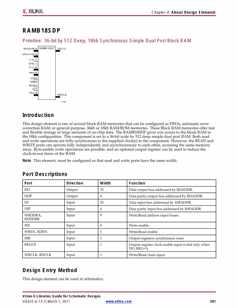
Chapter 4: About Design Elements
RAMB18SDPPrimitive: 36-bit by 512 Deep, 18kb Synchronous Simple Dual Port Block RAM
IntroductionThis design element is one of several block RAM memories that can be configured as FIFOs, automatic errorcorrection RAM, or general-purpose, 36kb or 18kb RAM/ROMmemories. These Block RAMmemories offer fastand flexible storage of large amounts of on-chip data. The RAMB18SDP gives you access to the block RAM inthe 18kb configuration. This component is set to a 36-bit wide by 512 deep simple dual port RAM. Both readand write operations are fully synchronous to the supplied clock(s) to the component. However, the READ andWRITE ports can operate fully independently and asynchronously to each other, accessing the same memoryarray. Byte-enable write operations are possible, and an optional output register can be used to reduce theclock-to-out times of the RAM.
Note This element, must be configured so that read and write ports have the same width.
Port DescriptionsPort Direction Width FunctionDO Output 32 Data output bus addressed by RDADDR.
DOP Output 4 Data parity output bus addressed by RDADDR.
DI Input 32 Data input bus addressed by WRADDR.
DIP Input 4 Data parity input bus addressed by WRADDR.
WRDDRA,RDDDRB
Input 9 Write/Read address input buses.
WE Input 4 Write enable.
WREN, RDEN Input 1 Write/Read enable
SSR Input 1 Output registers synchronous reset.
REGCE Input 1 Output register clock enable input (valid only whenDO_REG=1).
WRCLK, RDCLK Input 1 Write/Read clock input.
Design Entry MethodThis design element can be used in schematics.
Virtex-5 Libraries Guide for Schematic DesignsUG622 (v 13.1) March 1, 2011 www.xilinx.com 581
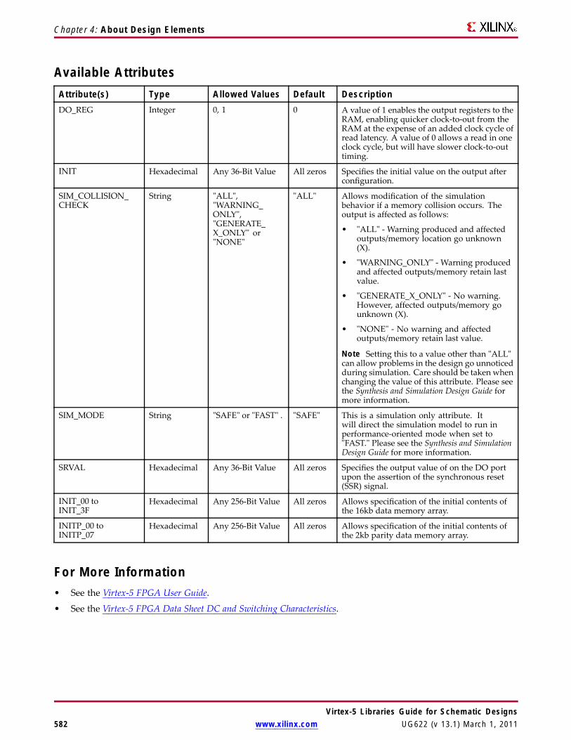
Chapter 4: About Design Elements
Available AttributesAttribute(s) Type Allowed Values Default DescriptionDO_REG Integer 0, 1 0 A value of 1 enables the output registers to the
RAM, enabling quicker clock-to-out from theRAM at the expense of an added clock cycle ofread latency. A value of 0 allows a read in oneclock cycle, but will have slower clock-to-outtiming.
INIT Hexadecimal Any 36-Bit Value All zeros Specifies the initial value on the output afterconfiguration.
SIM_COLLISION_CHECK
String "ALL","WARNING_ONLY","GENERATE_X_ONLY" or"NONE"
"ALL" Allows modification of the simulationbehavior if a memory collision occurs. Theoutput is affected as follows:
• "ALL" - Warning produced and affectedoutputs/memory location go unknown(X).
• "WARNING_ONLY" - Warning producedand affected outputs/memory retain lastvalue.
• "GENERATE_X_ONLY" - No warning.However, affected outputs/memory gounknown (X).
• "NONE" - No warning and affectedoutputs/memory retain last value.
Note Setting this to a value other than "ALL"can allow problems in the design go unnoticedduring simulation. Care should be taken whenchanging the value of this attribute. Please seethe Synthesis and Simulation Design Guide formore information.
SIM_MODE String "SAFE" or "FAST" . "SAFE" This is a simulation only attribute. Itwill direct the simulation model to run inperformance-oriented mode when set to"FAST." Please see the Synthesis and SimulationDesign Guide for more information.
SRVAL Hexadecimal Any 36-Bit Value All zeros Specifies the output value of on the DO portupon the assertion of the synchronous reset(SSR) signal.
INIT_00 toINIT_3F
Hexadecimal Any 256-Bit Value All zeros Allows specification of the initial contents ofthe 16kb data memory array.
INITP_00 toINITP_07
Hexadecimal Any 256-Bit Value All zeros Allows specification of the initial contents ofthe 2kb parity data memory array.
For More Information• See the Virtex-5 FPGA User Guide.
• See the Virtex-5 FPGA Data Sheet DC and Switching Characteristics.
Virtex-5 Libraries Guide for Schematic Designs582 www.xilinx.com UG622 (v 13.1) March 1, 2011

Chapter 4: About Design Elements
RAMB36Primitive: 36kb Configurable Synchronous True Dual Port Block RAM
IntroductionThis design element is one of several block RAM memories that can be configured as FIFOs, automatic errorcorrection RAM, or general-purpose, 36kb or 18kb RAM/ROM memories. These block RAM memories offerfast and flexible storage of large amounts of on-chip data. This element allows access to the block RAM in the36kb configuration. This component can be configured and used as a 1-bit wide by 32K deep to a 36-bit wide by1K deep true dual port RAM. Both read and write operations are fully synchronous to the supplied clock(s)to the component. However, Port A and Port B can operate fully independently and asynchronously to eachother accessing the same memory array. When configured in the wider data width modes, byte-enable writeoperations are possible and an option output register can be used to reduce the clock-to-out times of the RAM atthe expense of an extra clock cycle of latency.
This design element should be used for Simple Dual Port 72-bit wide, 512 deep, optional ECC scrub functionality.This element can be created using cascaded RAMB18s.
The following possible combination of elements can be placed in RAMB36:
• RAMB18/RAMB18
• RAMB18/FIFO18
• RAMB18SDP/RAMB18SDP
• RAMB18SDP/FIFO18_36
Virtex-5 Libraries Guide for Schematic DesignsUG622 (v 13.1) March 1, 2011 www.xilinx.com 583
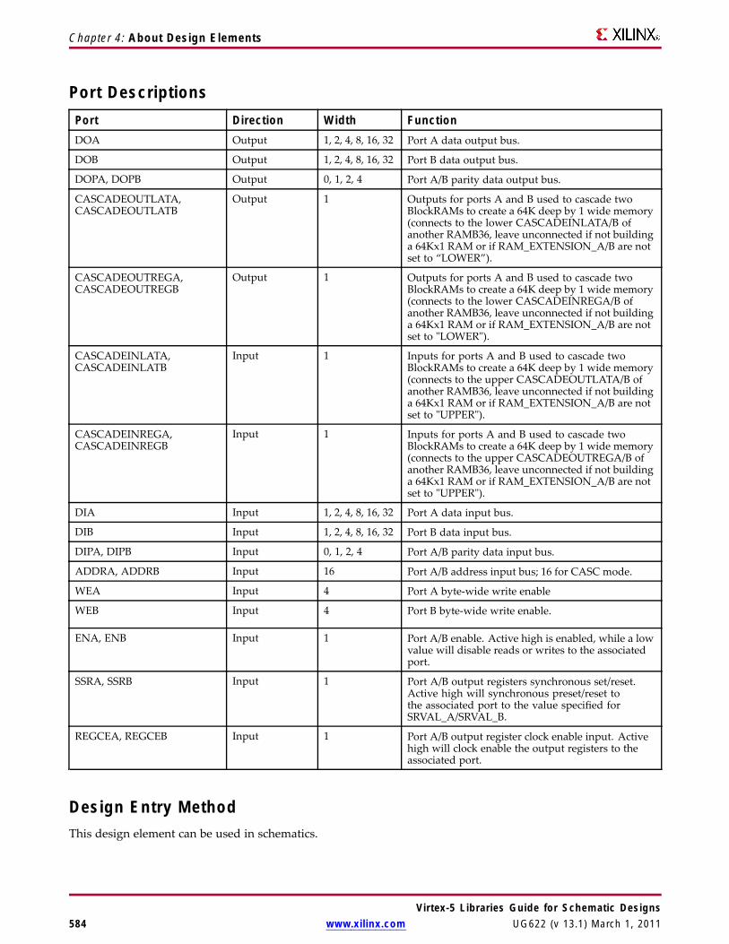
Chapter 4: About Design Elements
Port DescriptionsPort Direction Width FunctionDOA Output 1, 2, 4, 8, 16, 32 Port A data output bus.
DOB Output 1, 2, 4, 8, 16, 32 Port B data output bus.
DOPA, DOPB Output 0, 1, 2, 4 Port A/B parity data output bus.
CASCADEOUTLATA,CASCADEOUTLATB
Output 1 Outputs for ports A and B used to cascade twoBlockRAMs to create a 64K deep by 1 wide memory(connects to the lower CASCADEINLATA/B ofanother RAMB36, leave unconnected if not buildinga 64Kx1 RAM or if RAM_EXTENSION_A/B are notset to “LOWER”).
CASCADEOUTREGA,CASCADEOUTREGB
Output 1 Outputs for ports A and B used to cascade twoBlockRAMs to create a 64K deep by 1 wide memory(connects to the lower CASCADEINREGA/B ofanother RAMB36, leave unconnected if not buildinga 64Kx1 RAM or if RAM_EXTENSION_A/B are notset to "LOWER").
CASCADEINLATA,CASCADEINLATB
Input 1 Inputs for ports A and B used to cascade twoBlockRAMs to create a 64K deep by 1 wide memory(connects to the upper CASCADEOUTLATA/B ofanother RAMB36, leave unconnected if not buildinga 64Kx1 RAM or if RAM_EXTENSION_A/B are notset to "UPPER").
CASCADEINREGA,CASCADEINREGB
Input 1 Inputs for ports A and B used to cascade twoBlockRAMs to create a 64K deep by 1 wide memory(connects to the upper CASCADEOUTREGA/B ofanother RAMB36, leave unconnected if not buildinga 64Kx1 RAM or if RAM_EXTENSION_A/B are notset to "UPPER").
DIA Input 1, 2, 4, 8, 16, 32 Port A data input bus.
DIB Input 1, 2, 4, 8, 16, 32 Port B data input bus.
DIPA, DIPB Input 0, 1, 2, 4 Port A/B parity data input bus.
ADDRA, ADDRB Input 16 Port A/B address input bus; 16 for CASC mode.
WEA Input 4 Port A byte-wide write enable
WEB Input 4 Port B byte-wide write enable.
ENA, ENB Input 1 Port A/B enable. Active high is enabled, while a lowvalue will disable reads or writes to the associatedport.
SSRA, SSRB Input 1 Port A/B output registers synchronous set/reset.Active high will synchronous preset/reset tothe associated port to the value specified forSRVAL_A/SRVAL_B.
REGCEA, REGCEB Input 1 Port A/B output register clock enable input. Activehigh will clock enable the output registers to theassociated port.
Design Entry MethodThis design element can be used in schematics.
Virtex-5 Libraries Guide for Schematic Designs584 www.xilinx.com UG622 (v 13.1) March 1, 2011

Chapter 4: About Design Elements
The following table shows the necessary data, address and write enable connections for the variable width portsfor each DATA_WIDTH value for either Port A or Port B. If a different width is used for the read and write on thesame port, use the deeper of the two in order to select address connections.
All data and address ports not necessary for a particular configuration should either be left unconnected orgrounded with the following exceptions.
• The address bit 15 is only used in cascadable block RAM. For noncascading block RAM, connect High.
• ADDR pins must be 16-bits wide. However, valid addresses for non-cascadable block RAM are only foundon pin 14 to (15 - address width). The remaining pins, including pin 15, should be tied High.
DATA_WIDTHValue
DI, DIPConnections
ADDRConnections WE Connections
DO, DOPConnections
1 (with cascade) DI[0] ADDR[15:0] Connect WE[3:0] to single userWE signal
DO[0]
1 (without cascade) DI[0] ADDR[14:0] Connect WE[3:0] to single userWE signal
DO[0]
2 DI[1:0] ADDR[14:1] Connect WE[3:0] to single userWE signal
DO[1:0]
4 DI[3:0] ADDR[14:2] Connect WE[3:0] to single userWE signal
DO[3:0]
9 DI[7:0], DIP[0] ADDR[14:3] Connect WE[3:0] to single userWE signal
DO[7:0], DOP[0]
18 DI[15:0], DIP[1:0] ADDR[14:4] Connect WE[0] and WE[2] touser WE[0] and WE[1] andWE[3] to user WE[1]
DO[15:0], DOP[1:0]
36 DI[31:0], DIP[3:0] ADDR[14:5] Connect each WE[3:0] signalto the associated byte writeenable/
DO[31:0], DOP[3:0]
Available AttributesAttribute Type Allowed Values Default DescriptionDOA_REG,DOB_REG
Integer 0, 1 0 A value of 1 enables to the outputregisters to the RAM enabling quickerclock-to-out from the RAM at theexpense of an added clock cycle ofread latency. A value of 0 allows aread in one clock cycle, but will resultin slower clock to out timing.
INIT_A Hexadecimal Any 36-Bit Value All zeros Specifies the initial value on theoutput of Port A of the RAMB36 afterconfiguration.
INIT_B Hexadecimal Any 36-Bit Value All zeros Specifies the initial value on theoutput of Port B of the RAMB36 afterconfiguration.
READ_WIDTH_A Integer 0, 1, 4, 9, 18 or 36 0 Specifies the desired data width for aread on Port A, including parity bits.This value must be 0 if the Port B isnot used. Otherwise, it should be setto the desired port width.
Virtex-5 Libraries Guide for Schematic DesignsUG622 (v 13.1) March 1, 2011 www.xilinx.com 585

Chapter 4: About Design Elements
Attribute Type Allowed Values Default DescriptionREAD_WIDTH_B Integer 0, 1, 4, 9, 18 or 36 0 Specifies the desired data width for a
read on Port B including parity bits.This value must be 0 if the Port B isnot used. Otherwise, it should be setto the desired port width.
SIM_COLLISION_CHECK
String "ALL","WARNING_ONLY","GENERATE_X_ONLY" or"NONE"
"ALL” Allows modification of the simulationbehavior if a memory collision occurs.The output is affected as follows:
• "ALL" - Warning produced andaffected outputs/memory locationgo unknown (X).
• "WARNING_ONLY" - Warningproduced and affectedoutputs/memory retain lastvalue.
• "GENERATE_X_ONLY" - Nowarning. However, affectedoutputs/memory go unknown(X).
• "NONE" - No warning andaffected outputs/memory retainlast value.
Note Setting this to a value otherthan "ALL" can allow problems inthe design go unnoticed duringsimulation. Care should be takenwhen changing the value of thisattribute. Please see the Synthesisand Simulation Design Guide for moreinformation.
SIM_MODE String "SAFE" or "FAST" "SAFE" This is a simulation only attribute. Itwill direct the simulation model torun in performance-oriented modewhen set to "FAST." Please see theSynthesis and Simulation Design Guidefor more information.
SRVAL_A Hexadecimal Any 36-Bit Value All zeros Specifies the output value of theRAM upon the assertion of the Port Asynchronous reset (SSRA) signal.
SRVAL_B Hexadecimal Any 36-Bit Value All zeros Specifies the output value of theRAM upon the assertion of the Port Bsynchronous reset (SSRB) signal.
WRITE_MODE_A,WRITE_MODE_B
String "WRITE_FIRST","READ_FIRST" or"NO_CHANGE"
"WRITE_FIRST"
Specifies output behavior of the portbeing written to:
• "WRITE_FIRST" = written valueappears on output port of theRAM
• "READ_FIRST" = previous RAMcontents for that memory locationappear on the output port
• "NO_CHANGE" = previous valueon the output port remains thesame.
Virtex-5 Libraries Guide for Schematic Designs586 www.xilinx.com UG622 (v 13.1) March 1, 2011

Chapter 4: About Design Elements
Attribute Type Allowed Values Default DescriptionWRITE_WIDTH_A Integer 0, 1, 2, 4, 9, 18 or 36 0 Specifies the desired data width for a
write to Port B including parity bits.This value must be 0 if the port is notused. Otherwise should be set to thedesired write width.
WRITE_WIDTH_B Integer 0, 1, 2, 4, 9, 18 or 36 0 Specifies the desired data width for awrite to Port B including parity bits.This value must be 0 if the port is notused. Otherwise should be set to thedesired write width.
RAM_EXTENTION_A,RAM_ EXTENTION_B
String "UPPER","LOWER"or "NONE"
"NONE" If not cascading two BlockRAMs toform a 72K x 1 RAM set to NONE".If cascading RAMs, set to either"UPPER" or "LOWER" to indicaterelative RAM location for properconfiguration of the RAM.
INIT_00 toINIT_7F
Hexadecimal Any 256-Bit Value All zeros Allows specification of the initialcontents of the 72kb data memoryarray.
INITP_00 toINITP_0F
Hexadecimal Any 256-Bit Value All zeros Allows specification of the initialcontents of the 4kb parity datamemory array.
For More Information• See the Virtex-5 FPGA User Guide.
• See the Virtex-5 FPGA Data Sheet DC and Switching Characteristics.
Virtex-5 Libraries Guide for Schematic DesignsUG622 (v 13.1) March 1, 2011 www.xilinx.com 587
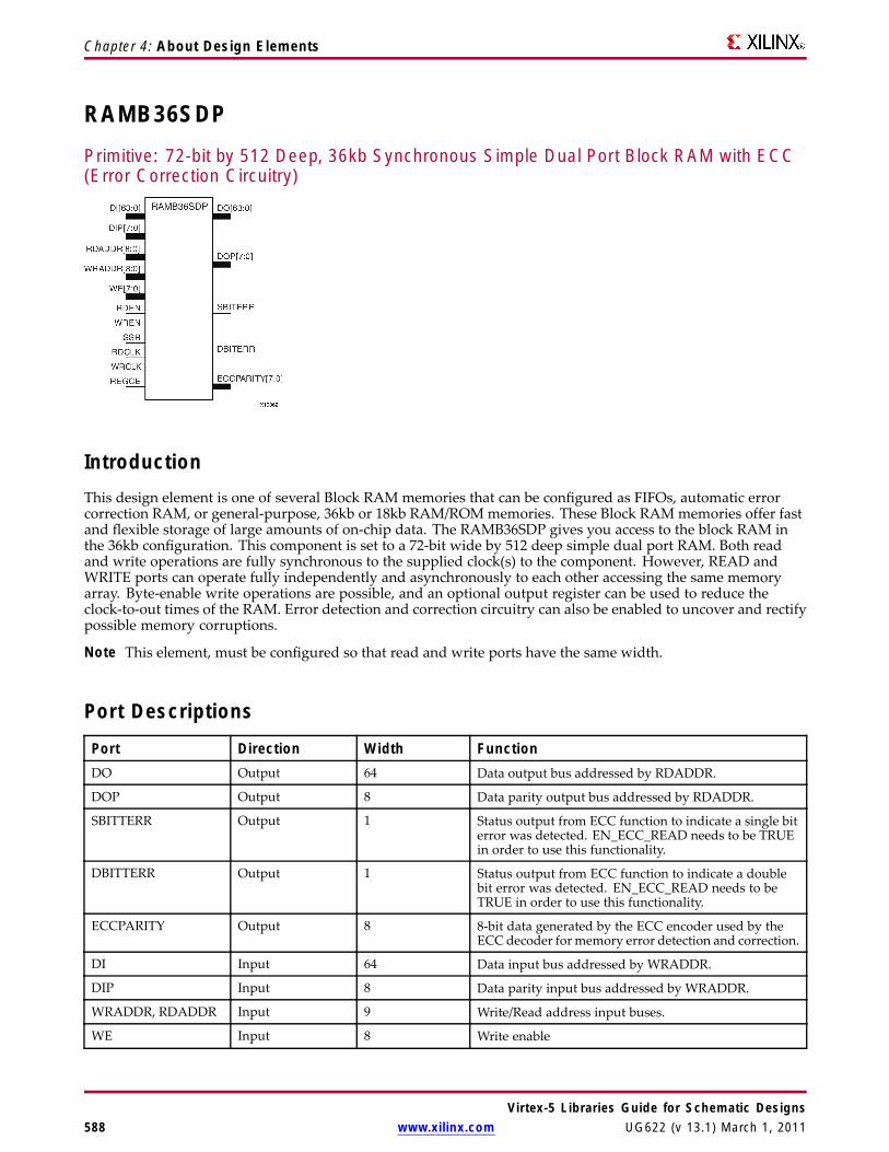
Chapter 4: About Design Elements
RAMB36SDPPrimitive: 72-bit by 512 Deep, 36kb Synchronous Simple Dual Port Block RAM with ECC(Error Correction Circuitry)
IntroductionThis design element is one of several Block RAM memories that can be configured as FIFOs, automatic errorcorrection RAM, or general-purpose, 36kb or 18kb RAM/ROMmemories. These Block RAMmemories offer fastand flexible storage of large amounts of on-chip data. The RAMB36SDP gives you access to the block RAM inthe 36kb configuration. This component is set to a 72-bit wide by 512 deep simple dual port RAM. Both readand write operations are fully synchronous to the supplied clock(s) to the component. However, READ andWRITE ports can operate fully independently and asynchronously to each other accessing the same memoryarray. Byte-enable write operations are possible, and an optional output register can be used to reduce theclock-to-out times of the RAM. Error detection and correction circuitry can also be enabled to uncover and rectifypossible memory corruptions.
Note This element, must be configured so that read and write ports have the same width.
Port Descriptions
Port Direction Width FunctionDO Output 64 Data output bus addressed by RDADDR.
DOP Output 8 Data parity output bus addressed by RDADDR.
SBITTERR Output 1 Status output from ECC function to indicate a single biterror was detected. EN_ECC_READ needs to be TRUEin order to use this functionality.
DBITTERR Output 1 Status output from ECC function to indicate a doublebit error was detected. EN_ECC_READ needs to beTRUE in order to use this functionality.
ECCPARITY Output 8 8-bit data generated by the ECC encoder used by theECC decoder for memory error detection and correction.
DI Input 64 Data input bus addressed by WRADDR.
DIP Input 8 Data parity input bus addressed by WRADDR.
WRADDR, RDADDR Input 9 Write/Read address input buses.
WE Input 8 Write enable
Virtex-5 Libraries Guide for Schematic Designs588 www.xilinx.com UG622 (v 13.1) March 1, 2011
Chapter 4: About Design Elements
Port Direction Width FunctionWREN, RDEN Input 1 Write/Read enable
SSR Input 1 Output registers synchronous reset.
REGCE Input 1 Output register clock enable input (valid only whenDO_REG=1)
WRCLK, RDCLK Input 1 Write/Read clock input.
Design Entry MethodThis design element can be used in schematics.
Available Attributes
Attribute TypeAllowedValues Default Description
DO_REG Integer 0, 1 0 A value of 1 enables to the output registers tothe RAM enabling quicker clock-to-out from theRAM at the expense of an added clock cycleof read latency. A value of 0 allows a read inone clock cycle but will have slower clock to outtiming.
INIT Hexadecimal Any 72-Bit Value All zeros Specifies the initial value on the output afterconfiguration.
EN_ECC_READ Boolean TRUE or FALSE FALSE Enable the ECC decoder circuitry.
EN_ECC_WRITE Boolean TRUE or FALSE FALSE Enable the ECC encoder circuitry.
EN_ECC_SCRUB Boolean TRUE or FALSE FALSE Enable ECC scrubbing of RAM contents
SIM_COLLISION_CHECK
String "ALL","WARNING_ONLY","GENERATE_X_ ONLY"or "NONE"
"ALL" Allows modification of the simulation behaviorif a memory collision occurs. The output isaffected as follows:
• "ALL" - Warning produced and affectedoutputs/memory location go unknown (X).
• "WARNING_ONLY" - Warning producedand affected outputs/memory retain lastvalue.
• "GENERATE_X_ONLY" - No warning.However, affected outputs/memory gounknown (X).
• "NONE" - No warning and affectedoutputs/memory retain last value.
Note Setting this to a value other than "ALL"can allow problems in the design go unnoticedduring simulation. Care should be taken whenchanging the value of this attribute. Please seethe Synthesis and Simulation Design Guide formore information.
SIM_MODE String "SAFE" or"FAST" .
"SAFE" This is a simulation only attribute. Itwill direct the simulation model to run inperformance-oriented mode when set to "FAST."Please see the Synthesis and Simulation DesignGuide for more information.
Virtex-5 Libraries Guide for Schematic DesignsUG622 (v 13.1) March 1, 2011 www.xilinx.com 589
Chapter 4: About Design Elements
Attribute TypeAllowedValues Default Description
SRVAL Hexadecimal Any 72-Bit Value All zeroes Specifies the output value of on the DO portupon the assertion of the synchronous reset(SSR) signal.
INIT_00 toINIT_3F
Hexadecimal Any 256-BitValue
All zeroes Allows specification of the initial contents of the16kb data memory array.
INITP_00 toINITP_07
Hexadecimal Any 256-BitValue
All zeroes Allows specification of the initial contents of the2kb parity data memory array.
For More Information• See the Virtex-5 FPGA User Guide.
• See the Virtex-5 FPGA Data Sheet DC and Switching Characteristics.
Virtex-5 Libraries Guide for Schematic Designs590 www.xilinx.com UG622 (v 13.1) March 1, 2011

Chapter 4: About Design Elements
ROM128X1Primitive: 128-Deep by 1-Wide ROM
IntroductionThis design element is a 128-word by 1-bit read-only memory. The data output (O) reflects the word selected bythe 7-bit address (A6:A0). The ROM is initialized to a known value during configuration with the INIT=valueparameter. The value consists of 32 hexadecimal digits that are written into the ROM from the most-significantdigit A=FH to the least-significant digit A=0H. An error occurs if the INIT=value is not specified.
Logic TableInput Output
I0 I1 I2 I3 O0 0 0 0 INIT(0)
0 0 0 1 INIT(1)
0 0 1 0 INIT(2)
0 0 1 1 INIT(3)
0 1 0 0 INIT(4)
0 1 0 1 INIT(5)
0 1 1 0 INIT(6)
0 1 1 1 INIT(7)
1 0 0 0 INIT(8)
1 0 0 1 INIT(9)
1 0 1 0 INIT(10)
1 0 1 1 INIT(11)
1 1 0 0 INIT(12)
1 1 0 1 INIT(13)
1 1 1 0 INIT(14)
1 1 1 1 INIT(15)
Design Entry MethodThis design element can be used in schematics.
Virtex-5 Libraries Guide for Schematic DesignsUG622 (v 13.1) March 1, 2011 www.xilinx.com 591

Chapter 4: About Design Elements
Available AttributesAttribute Type Allowed Values Default DescriptionINIT Hexadecimal Any 128-Bit Value All zeros Specifies the contents of the ROM.
For More Information• See the Virtex-5 FPGA User Guide.
• See the Virtex-5 FPGA Data Sheet DC and Switching Characteristics.
Virtex-5 Libraries Guide for Schematic Designs592 www.xilinx.com UG622 (v 13.1) March 1, 2011
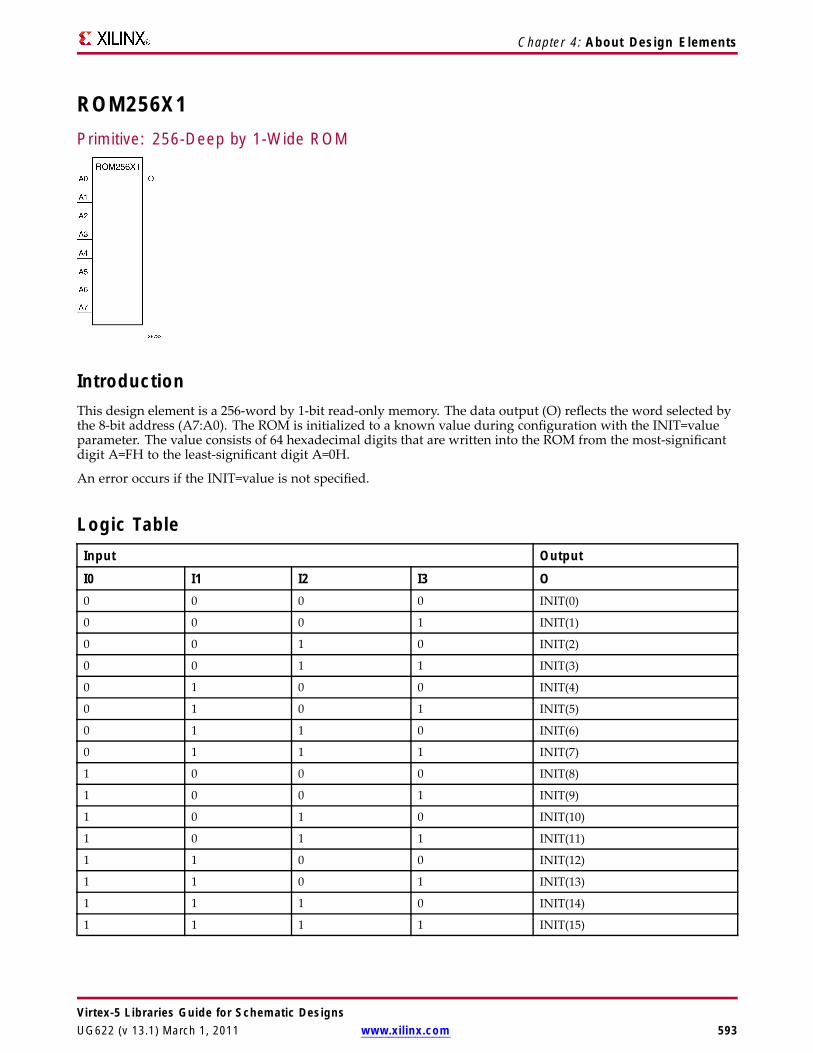
Chapter 4: About Design Elements
ROM256X1Primitive: 256-Deep by 1-Wide ROM
IntroductionThis design element is a 256-word by 1-bit read-only memory. The data output (O) reflects the word selected bythe 8-bit address (A7:A0). The ROM is initialized to a known value during configuration with the INIT=valueparameter. The value consists of 64 hexadecimal digits that are written into the ROM from the most-significantdigit A=FH to the least-significant digit A=0H.
An error occurs if the INIT=value is not specified.
Logic TableInput Output
I0 I1 I2 I3 O0 0 0 0 INIT(0)
0 0 0 1 INIT(1)
0 0 1 0 INIT(2)
0 0 1 1 INIT(3)
0 1 0 0 INIT(4)
0 1 0 1 INIT(5)
0 1 1 0 INIT(6)
0 1 1 1 INIT(7)
1 0 0 0 INIT(8)
1 0 0 1 INIT(9)
1 0 1 0 INIT(10)
1 0 1 1 INIT(11)
1 1 0 0 INIT(12)
1 1 0 1 INIT(13)
1 1 1 0 INIT(14)
1 1 1 1 INIT(15)
Virtex-5 Libraries Guide for Schematic DesignsUG622 (v 13.1) March 1, 2011 www.xilinx.com 593

Chapter 4: About Design Elements
Design Entry MethodThis design element can be used in schematics.
Available AttributesAttribute Type Allowed Values Default DescriptionINIT Hexadecimal Any 256-Bit Value All zeros Specifies the contents of the ROM.
For More Information• See the Virtex-5 FPGA User Guide.
• See the Virtex-5 FPGA Data Sheet DC and Switching Characteristics.
Virtex-5 Libraries Guide for Schematic Designs594 www.xilinx.com UG622 (v 13.1) March 1, 2011
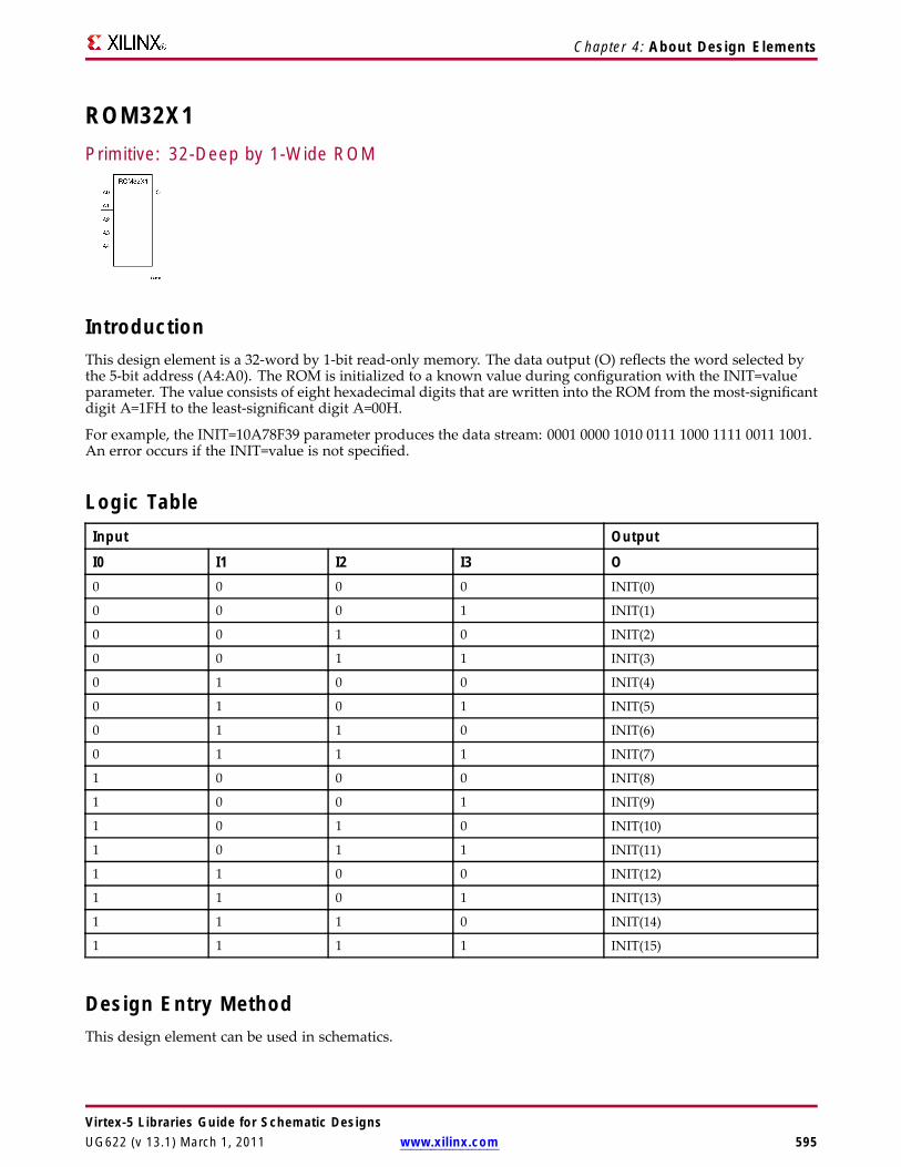
Chapter 4: About Design Elements
ROM32X1Primitive: 32-Deep by 1-Wide ROM
IntroductionThis design element is a 32-word by 1-bit read-only memory. The data output (O) reflects the word selected bythe 5-bit address (A4:A0). The ROM is initialized to a known value during configuration with the INIT=valueparameter. The value consists of eight hexadecimal digits that are written into the ROM from the most-significantdigit A=1FH to the least-significant digit A=00H.
For example, the INIT=10A78F39 parameter produces the data stream: 0001 0000 1010 0111 1000 1111 0011 1001.An error occurs if the INIT=value is not specified.
Logic TableInput Output
I0 I1 I2 I3 O0 0 0 0 INIT(0)
0 0 0 1 INIT(1)
0 0 1 0 INIT(2)
0 0 1 1 INIT(3)
0 1 0 0 INIT(4)
0 1 0 1 INIT(5)
0 1 1 0 INIT(6)
0 1 1 1 INIT(7)
1 0 0 0 INIT(8)
1 0 0 1 INIT(9)
1 0 1 0 INIT(10)
1 0 1 1 INIT(11)
1 1 0 0 INIT(12)
1 1 0 1 INIT(13)
1 1 1 0 INIT(14)
1 1 1 1 INIT(15)
Design Entry MethodThis design element can be used in schematics.
Virtex-5 Libraries Guide for Schematic DesignsUG622 (v 13.1) March 1, 2011 www.xilinx.com 595

Chapter 4: About Design Elements
Available AttributesAttribute Type Allowed Values Default DescriptionINIT Hexadecimal Any 32-Bit Value All zeros Specifies the contents of the ROM.
For More Information• See the Virtex-5 FPGA User Guide.
• See the Virtex-5 FPGA Data Sheet DC and Switching Characteristics.
Virtex-5 Libraries Guide for Schematic Designs596 www.xilinx.com UG622 (v 13.1) March 1, 2011

Chapter 4: About Design Elements
ROM64X1Primitive: 64-Deep by 1-Wide ROM
IntroductionThis design element is a 64-word by 1-bit read-only memory. The data output (O) reflects the word selected bythe 6-bit address (A5:A0). The ROM is initialized to a known value during configuration with the INIT=valueparameter. The value consists of 16 hexadecimal digits that are written into the ROM from the most-significantdigit A=FH to the least-significant digit A=0H. An error occurs if the INIT=value is not specified.
Logic TableInput Output
I0 I1 I2 I3 O0 0 0 0 INIT(0)
0 0 0 1 INIT(1)
0 0 1 0 INIT(2)
0 0 1 1 INIT(3)
0 1 0 0 INIT(4)
0 1 0 1 INIT(5)
0 1 1 0 INIT(6)
0 1 1 1 INIT(7)
1 0 0 0 INIT(8)
1 0 0 1 INIT(9)
1 0 1 0 INIT(10)
1 0 1 1 INIT(11)
1 1 0 0 INIT(12)
1 1 0 1 INIT(13)
1 1 1 0 INIT(14)
1 1 1 1 INIT(15)
Design Entry MethodThis design element can be used in schematics.
Virtex-5 Libraries Guide for Schematic DesignsUG622 (v 13.1) March 1, 2011 www.xilinx.com 597

Chapter 4: About Design Elements
Available AttributesAttribute Type Allowed Values Default DescriptionINIT Hexadecimal Any 64-Bit Value All zeros Specifies the contents of the ROM.
For More Information• See the Virtex-5 FPGA User Guide.
• See the Virtex-5 FPGA Data Sheet DC and Switching Characteristics.
Virtex-5 Libraries Guide for Schematic Designs598 www.xilinx.com UG622 (v 13.1) March 1, 2011

Chapter 4: About Design Elements
SOP3Macro: 3–Input Sum of Products
IntroductionThree input Sum of Products (SOP) macros provide common logic functions by OR gating the output of oneAND function with one direct input. Variations of inverting and non-inverting inputs are available.
Design Entry MethodThis design element is only for use in schematics.
For More Information• See the Virtex-5 FPGA User Guide.
• See the Virtex-5 FPGA Data Sheet DC and Switching Characteristics.
Virtex-5 Libraries Guide for Schematic DesignsUG622 (v 13.1) March 1, 2011 www.xilinx.com 599
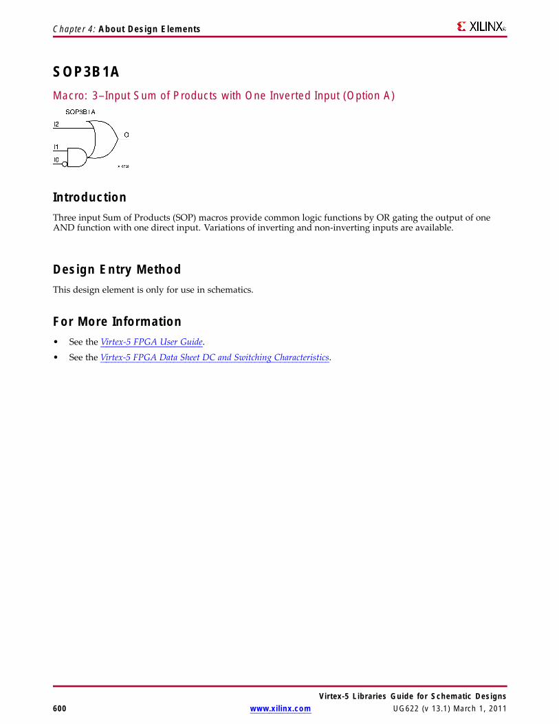
Chapter 4: About Design Elements
SOP3B1AMacro: 3–Input Sum of Products with One Inverted Input (Option A)
IntroductionThree input Sum of Products (SOP) macros provide common logic functions by OR gating the output of oneAND function with one direct input. Variations of inverting and non-inverting inputs are available.
Design Entry MethodThis design element is only for use in schematics.
For More Information• See the Virtex-5 FPGA User Guide.
• See the Virtex-5 FPGA Data Sheet DC and Switching Characteristics.
Virtex-5 Libraries Guide for Schematic Designs600 www.xilinx.com UG622 (v 13.1) March 1, 2011

Chapter 4: About Design Elements
SOP3B1BMacro: 3–Input Sum of Products with One Inverted Input (Option B)
IntroductionThree input Sum of Products (SOP) macros provide common logic functions by OR gating the output of oneAND function with one direct input. Variations of inverting and non-inverting inputs are available.
Design Entry MethodThis design element is only for use in schematics.
For More Information• See the Virtex-5 FPGA User Guide.
• See the Virtex-5 FPGA Data Sheet DC and Switching Characteristics.
Virtex-5 Libraries Guide for Schematic DesignsUG622 (v 13.1) March 1, 2011 www.xilinx.com 601

Chapter 4: About Design Elements
SOP3B2AMacro: 3–Input Sum of Products with Two Inverted Inputs (Option A)
IntroductionThree input Sum of Products (SOP) macros provide common logic functions by OR gating the output of oneAND function with one direct input. Variations of inverting and non-inverting inputs are available.
Design Entry MethodThis design element is only for use in schematics.
For More Information• See the Virtex-5 FPGA User Guide.
• See the Virtex-5 FPGA Data Sheet DC and Switching Characteristics.
Virtex-5 Libraries Guide for Schematic Designs602 www.xilinx.com UG622 (v 13.1) March 1, 2011

Chapter 4: About Design Elements
SOP3B2BMacro: 3–Input Sum of Products with Two Inverted Inputs (Option B)
IntroductionThree input Sum of Products (SOP) macros provide common logic functions by OR gating the output of oneAND function with one direct input. Variations of inverting and non-inverting inputs are available.
Design Entry MethodThis design element is only for use in schematics.
For More Information• See the Virtex-5 FPGA User Guide.
• See the Virtex-5 FPGA Data Sheet DC and Switching Characteristics.
Virtex-5 Libraries Guide for Schematic DesignsUG622 (v 13.1) March 1, 2011 www.xilinx.com 603

Chapter 4: About Design Elements
SOP3B3Macro: 3–Input Sum of Products with Inverted Inputs
IntroductionThree input Sum of Products (SOP) macros provide common logic functions by OR gating the output of oneAND function with one direct input. Variations of inverting and non-inverting inputs are available.
Design Entry MethodThis design element is only for use in schematics.
For More Information• See the Virtex-5 FPGA User Guide.
• See the Virtex-5 FPGA Data Sheet DC and Switching Characteristics.
Virtex-5 Libraries Guide for Schematic Designs604 www.xilinx.com UG622 (v 13.1) March 1, 2011

Chapter 4: About Design Elements
SOP4Macro: 4–Input Sum of Products
IntroductionFour input Sum of Products (SOP) macros provide common logic functions by OR gating the outputs of twoAND functions. Variations of inverting and non-inverting inputs are available.
Design Entry MethodThis design element is only for use in schematics.
For More Information• See the Virtex-5 FPGA User Guide.
• See the Virtex-5 FPGA Data Sheet DC and Switching Characteristics.
Virtex-5 Libraries Guide for Schematic DesignsUG622 (v 13.1) March 1, 2011 www.xilinx.com 605

Chapter 4: About Design Elements
SOP4B1Macro: 4–Input Sum of Products with One Inverted Input
IntroductionFour input Sum of Products (SOP) macros provide common logic functions by OR gating the outputs of twoAND functions. Variations of inverting and non-inverting inputs are available.
Design Entry MethodThis design element is only for use in schematics.
For More Information• See the Virtex-5 FPGA User Guide.
• See the Virtex-5 FPGA Data Sheet DC and Switching Characteristics.
Virtex-5 Libraries Guide for Schematic Designs606 www.xilinx.com UG622 (v 13.1) March 1, 2011

Chapter 4: About Design Elements
SOP4B2AMacro: 4–Input Sum of Products with Two Inverted Inputs (Option A)
IntroductionFour input Sum of Products (SOP) macros provide common logic functions by OR gating the outputs of twoAND functions. Variations of inverting and non-inverting inputs are available.
Design Entry MethodThis design element is only for use in schematics.
For More Information• See the Virtex-5 FPGA User Guide.
• See the Virtex-5 FPGA Data Sheet DC and Switching Characteristics.
Virtex-5 Libraries Guide for Schematic DesignsUG622 (v 13.1) March 1, 2011 www.xilinx.com 607
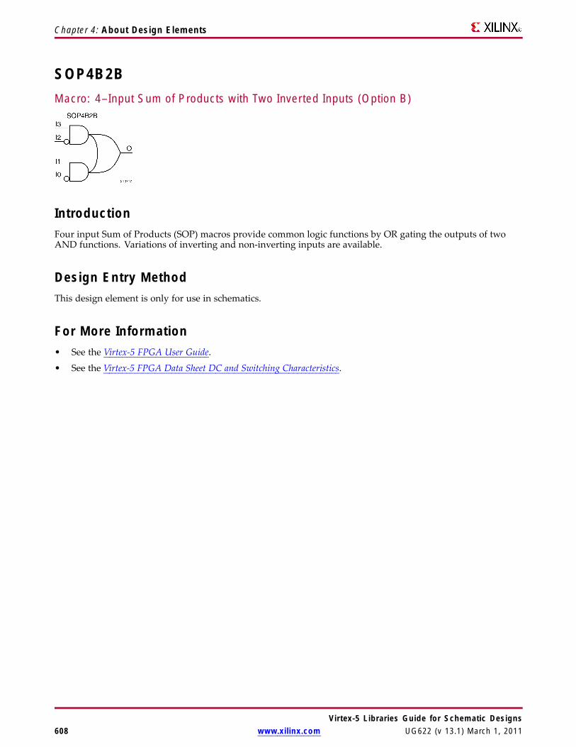
Chapter 4: About Design Elements
SOP4B2BMacro: 4–Input Sum of Products with Two Inverted Inputs (Option B)
IntroductionFour input Sum of Products (SOP) macros provide common logic functions by OR gating the outputs of twoAND functions. Variations of inverting and non-inverting inputs are available.
Design Entry MethodThis design element is only for use in schematics.
For More Information• See the Virtex-5 FPGA User Guide.
• See the Virtex-5 FPGA Data Sheet DC and Switching Characteristics.
Virtex-5 Libraries Guide for Schematic Designs608 www.xilinx.com UG622 (v 13.1) March 1, 2011
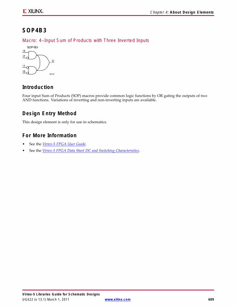
Chapter 4: About Design Elements
SOP4B3Macro: 4–Input Sum of Products with Three Inverted Inputs
IntroductionFour input Sum of Products (SOP) macros provide common logic functions by OR gating the outputs of twoAND functions. Variations of inverting and non-inverting inputs are available.
Design Entry MethodThis design element is only for use in schematics.
For More Information• See the Virtex-5 FPGA User Guide.
• See the Virtex-5 FPGA Data Sheet DC and Switching Characteristics.
Virtex-5 Libraries Guide for Schematic DesignsUG622 (v 13.1) March 1, 2011 www.xilinx.com 609

Chapter 4: About Design Elements
SOP4B4Macro: 4–Input Sum of Products with Inverted Inputs
IntroductionFour input Sum of Products (SOP) macros provide common logic functions by OR gating the outputs of twoAND functions. Variations of inverting and non-inverting inputs are available.
Design Entry MethodThis design element is only for use in schematics.
For More Information• See the Virtex-5 FPGA User Guide.
• See the Virtex-5 FPGA Data Sheet DC and Switching Characteristics.
Virtex-5 Libraries Guide for Schematic Designs610 www.xilinx.com UG622 (v 13.1) March 1, 2011

Chapter 4: About Design Elements
SR16CEMacro: 16-Bit Serial-In Parallel-Out Shift Register with Clock Enable and AsynchronousClear
IntroductionThis design element is a shift register with a shift-left serial input (SLI), parallel outputs (Q), and clock enable(CE) and asynchronous clear (CLR) inputs. The (CLR) input, when High, overrides all other inputs and resets thedata outputs (Q) Low. When (CE) is High and (CLR) is Low, the data on the SLI input is loaded into the firstbit of the shift register during the Low-to- High clock (C) transition and appears on the (Q0) output. Duringsubsequent Low-to- High clock transitions, when (CE) is High and (CLR) is Low, data shifts to the next highestbit position as new data is loaded into (Q0) (SLI→Q0, Q0→Q1, Q1→Q2, and so forth). The register ignores clocktransitions when (CE) is Low.
Registers can be cascaded by connecting the last (Q) output of one stage to the SLI input of the next stageand connecting clock, (CE), and (CLR) in parallel.
This register is asynchronously cleared, outputs Low, when power is applied. For FPGA devices, power-onconditions are simulated when global set/reset (GSR) is active. GSR defaults to active-High but can be invertedby adding an inverter in front of the GSR input of the appropriate STARTUP_architecture symbol.
Logic TableInputs Outputs
CLR CE SLI C Q0 Qz : Q11 X X X 0 0
0 0 X X No Change No Change
0 1 SLI ↑ SLI qn-1
z = bit width - 1
qn-1 = state of referenced output one setup time prior to active clock transition
Design Entry MethodThis design element is only for use in schematics.
For More Information• See the Virtex-5 FPGA User Guide.
• See the Virtex-5 FPGA Data Sheet DC and Switching Characteristics.
Virtex-5 Libraries Guide for Schematic DesignsUG622 (v 13.1) March 1, 2011 www.xilinx.com 611

Chapter 4: About Design Elements
SR16CLEMacro: 16-Bit Loadable Serial/Parallel-In Parallel-Out Shift Register with Clock Enableand Asynchronous Clear
IntroductionThis design element is a shift register with a shift-left serial input (SLI), parallel inputs (D), parallel outputs (Q),and three control inputs: clock enable (CE), load enable (L), and asynchronous clear (CLR) . The register ignoresclock transitions when (L) and (CE) are Low. The asynchronous (CLR), when High, overrides all other inputsand resets the data outputs (Q) Low. When (L) is High and (CLR) is Low, data on the Dn -D0 inputs is loadedinto the corresponding Qn -(Q0) bits of the register.
When (CE) is High and (L) and (CLR) are Low, data on the SLI input is loaded into the first bit of the shiftregister during the Low-to-High clock (C) transition and appears on the (Q0) output. During subsequent clocktransitions, when (CE) is High and (L) and (CLR) are Low, the data shifts to the next highest bit position as newdata is loaded into (Q)0 (for example, SLI→Q0, Q0→Q1, and Q1→Q2).
Registers can be cascaded by connecting the last (Q) output of one stage to the SLI input of the next stage andconnecting clock, (CE), (L), and (CLR) inputs in parallel.
This register is asynchronously cleared, outputs Low, when power is applied. For FPGA devices, power-onconditions are simulated when global set/reset (GSR) is active. GSR defaults to active-High but can be invertedby adding an inverter in front of the GSR input of the appropriate STARTUP_architecture symbol.
Logic TableInputs Outputs
CLR L CE SLI Dn : D0 C Q0 Qz : Q11 X X X X X 0 0
0 1 X X Dn : D0 ↑ D0 Dn
0 0 1 SLI X ↑ SLI qn-1
0 0 0 X X X No Change No Change
z = bitwidth -1
qn-1 = state of referenced output one setup time prior to active clock transition
Design Entry MethodThis design element is only for use in schematics.
Virtex-5 Libraries Guide for Schematic Designs612 www.xilinx.com UG622 (v 13.1) March 1, 2011

Chapter 4: About Design Elements
For More Information• See the Virtex-5 FPGA User Guide.
• See the Virtex-5 FPGA Data Sheet DC and Switching Characteristics.
Virtex-5 Libraries Guide for Schematic DesignsUG622 (v 13.1) March 1, 2011 www.xilinx.com 613

Chapter 4: About Design Elements
SR16CLEDMacro: 16-Bit Shift Register with Clock Enable and Asynchronous Clear
IntroductionThis design element is a shift register with shift-left (SLI) and shift-right (SRI) serial inputs, parallel inputs (D),parallel outputs (Q), and four control inputs: clock enable (CE), load enable (L), shift left/right (LEFT), andasynchronous clear (CLR). The register ignores clock transitions when (CE) and (L) are Low. The asynchronousclear, when High, overrides all other inputs and resets the data outputs (Qn) Low.
When (L) is High and (CLR) is Low, the data on the (D) inputs is loaded into the corresponding (Q) bits of theregister. When (CE) is High and (L) and (CLR) are Low, data is shifted right or left, depending on the state of theLEFT input. If LEFT is High, data on the SLI is loaded into (Q0) during the Low-to-High clock transition andshifted left (for example, to Q1 or Q2) during subsequent clock transitions. If LEFT is Low, data on the SRI isloaded into the last (Q) output during the Low-to-High clock transition and shifted right during subsequentclock transitions. The logic tables indicate the state of the (Q) outputs under all input conditions.
This register is asynchronously cleared, outputs Low, when power is applied. For FPGA devices, power-onconditions are simulated when global set/reset (GSR) is active. GSR defaults to active-High but can be invertedby adding an inverter in front of the GSR input of the appropriate STARTUP_architecture symbol.
Logic TableInputs Outputs
CLR L CE LEFT SLI SRID15 :D0 C Q0 Q15
Q14 :Q1
1 X X X X X X X 0 0 0
0 1 X X X X D15 : D0 ↑ D0 D15 Dn
0 0 0 X X X X X NoChange
NoChange
NoChange
0 0 1 1 SLI X X ↑ SLI q14 qn-1
0 0 1 0 X SRI X ↑ q1 SRI qn+1
qn-1 or qn+1 = state of referenced output one setup time prior to active clock transition.
Design Entry MethodThis design element is only for use in schematics.
Virtex-5 Libraries Guide for Schematic Designs614 www.xilinx.com UG622 (v 13.1) March 1, 2011

Chapter 4: About Design Elements
For More Information• See the Virtex-5 FPGA User Guide.
• See the Virtex-5 FPGA Data Sheet DC and Switching Characteristics.
Virtex-5 Libraries Guide for Schematic DesignsUG622 (v 13.1) March 1, 2011 www.xilinx.com 615

Chapter 4: About Design Elements
SR16REMacro: 16-Bit Serial-In Parallel-Out Shift Register with Clock Enable and SynchronousReset
IntroductionThis design element is a shift register with shift-left serial input (SLI), parallel outputs (Qn), clock enable (CE),and synchronous reset (R) inputs. The R input, when High, overrides all other inputs during the Low-to-Highclock (C) transition and resets the data outputs (Q) Low.
When (CE) is High and (R) is Low, the data on the (SLI) is loaded into the first bit of the shift register duringthe Low-to-High clock (C) transition and appears on the (Q0) output. During subsequent Low-to-High clocktransitions, when (CE) is High and R is Low, data shifts to the next highest bit position as new data is loaded into(Q0) (for example, SLI→Q0, Q0→Q1, and Q1→Q2). The register ignores clock transitions when (CE) is Low.
Registers can be cascaded by connecting the last (Q) output of one stage to the SLI input of the next stage andconnecting clock, (CE), and (R) in parallel.
This register is asynchronously cleared, outputs Low, when power is applied. For FPGA devices, power-onconditions are simulated when global set/reset (GSR) is active. GSR defaults to active-High but can be invertedby adding an inverter in front of the GSR input of the appropriate STARTUP_architecture symbol.
Logic TableInputs Outputs
R CE SLI C Q0 Qz : Q11 X X ↑ 0 0
0 0 X X No Change No Change
0 1 SLI ↑ SLI qn-1
z = bitwidth -1
qn-1 = state of referenced output one setup time prior to active clock transition
Design Entry MethodThis design element is only for use in schematics.
For More Information• See the Virtex-5 FPGA User Guide.
• See the Virtex-5 FPGA Data Sheet DC and Switching Characteristics.
Virtex-5 Libraries Guide for Schematic Designs616 www.xilinx.com UG622 (v 13.1) March 1, 2011

Chapter 4: About Design Elements
SR16RLEMacro: 16-Bit Loadable Serial/Parallel-In Parallel-Out Shift Register with Clock Enableand Synchronous Reset
IntroductionThis design element is a shift register with shift-left serial input (SLI), parallel inputs (D), parallel outputs (Q),and three control inputs: clock enable (CE), load enable (L), and synchronous reset (R). The register ignores clocktransitions when (L) and (CE) are Low. The synchronous (R), when High, overrides all other inputs during theLow-to-High clock (C) transition and resets the data outputs (Q) Low. When (L) is High and (R) is Low duringthe Low-to-High clock transition, data on the (D) inputs is loaded into the corresponding Q bits of the register.
When (CE) is High and (L) and (R) are Low, data on the (SLI) input is loaded into the first bit of the shiftregister during the Low-to-High clock (C) transition and appears on the Q0 output. During subsequent clocktransitions, when (CE) is High and (L) and (R) are Low, the data shifts to the next highest bit position as newdata is loaded into Q0.
Registers can be cascaded by connecting the last Q output of one stage to the SLI input of the next stage andconnecting clock, (CE), (L), and (R) inputs in parallel.
This register is asynchronously cleared, outputs Low, when power is applied. For FPGA devices, power-onconditions are simulated when global set/reset (GSR) is active. GSR defaults to active-High but can be invertedby adding an inverter in front of the GSR input of the appropriate STARTUP_architecture symbol.
Logic TableInputs Outputs
R L CE SLI Dz : D0 C Q0 Qz : Q11 X X X X ↑ 0 0
0 1 X X Dz : D0 ↑ D0 Dn
0 0 1 SLI X ↑ SLI qn-1
0 0 0 X X X No Change No Change
z = bitwidth -1
qn-1 = state of referenced output one setup time prior to active clock transition
Design Entry MethodThis design element is only for use in schematics.
Virtex-5 Libraries Guide for Schematic DesignsUG622 (v 13.1) March 1, 2011 www.xilinx.com 617

Chapter 4: About Design Elements
For More Information• See the Virtex-5 FPGA User Guide.
• See the Virtex-5 FPGA Data Sheet DC and Switching Characteristics.
Virtex-5 Libraries Guide for Schematic Designs618 www.xilinx.com UG622 (v 13.1) March 1, 2011

Chapter 4: About Design Elements
SR16RLEDMacro: 16-Bit Shift Register with Clock Enable and Synchronous Reset
IntroductionThis design element is a shift register with shift-left (SLI) and shift-right (SRI) serial inputs, parallel inputs (D),parallel outputs (Q) and four control inputs — clock enable (CE), load enable (L), shift left/right (LEFT), andsynchronous reset (R). The register ignores clock transitions when (CE) and (L) are Low. The synchronous (R),when High, overrides all other inputs during the Low-to-High clock (C) transition and resets the data outputs(Q) Low. When (L) is High and (R) is Low during the Low-to-High clock transition, the data on the (D) inputs isloaded into the corresponding (Q) bits of the register.
When (CE) is High and (L) and (R) are Low, data shifts right or left, depending on the state of the LEFT input.If LEFT is High, data on (SLI) is loaded into (Q0) during the Low-to-High clock transition and shifted left (forexample, to Q1 and Q2) during subsequent clock transitions. If LEFT is Low, data on the (SRI) is loaded into thelast (Q) output during the Low-to-High clock transition and shifted right ) during subsequent clock transitions.The logic tables below indicates the state of the (Q) outputs under all input conditions.
This register is asynchronously cleared, outputs Low, when power is applied. For FPGA devices, power-onconditions are simulated when global set/reset (GSR) is active. GSR defaults to active-High but can be invertedby adding an inverter in front of the GSR input of the appropriate STARTUP_architecture symbol.
Logic TableInputs Outputs
R L CE LEFT SLI SRI D15:D0 C Q0 Q15 Q14:Q11 X X X X X X ↑ 0 0 0
0 1 X X X X D15:D0 ↓ D0 D15 Dn
0 0 0 X X X X X NoChange
NoChange
NoChange
0 0 1 1 SLI X X ↑ SLI q14 qn-1
0 0 1 0 X SRI X ↓ q1 SRI qn+1
qn-1 or qn+1 = state of referenced output one setup time prior to active clock transition
Design Entry MethodThis design element is only for use in schematics.
Virtex-5 Libraries Guide for Schematic DesignsUG622 (v 13.1) March 1, 2011 www.xilinx.com 619

Chapter 4: About Design Elements
For More Information• See the Virtex-5 FPGA User Guide.
• See the Virtex-5 FPGA Data Sheet DC and Switching Characteristics.
Virtex-5 Libraries Guide for Schematic Designs620 www.xilinx.com UG622 (v 13.1) March 1, 2011

Chapter 4: About Design Elements
SR4CEMacro: 4-Bit Serial-In Parallel-Out Shift Register with Clock Enable and AsynchronousClear
IntroductionThis design element is a shift register with a shift-left serial input (SLI), parallel outputs (Q), and clock enable(CE) and asynchronous clear (CLR) inputs. The (CLR) input, when High, overrides all other inputs and resets thedata outputs (Q) Low. When (CE) is High and (CLR) is Low, the data on the SLI input is loaded into the firstbit of the shift register during the Low-to- High clock (C) transition and appears on the (Q0) output. Duringsubsequent Low-to- High clock transitions, when (CE) is High and (CLR) is Low, data shifts to the next highestbit position as new data is loaded into (Q0) (SLI→Q0, Q0→Q1, Q1→Q2, and so forth). The register ignores clocktransitions when (CE) is Low.
Registers can be cascaded by connecting the last (Q) output of one stage to the SLI input of the next stageand connecting clock, (CE), and (CLR) in parallel.
This register is asynchronously cleared, outputs Low, when power is applied. For FPGA devices, power-onconditions are simulated when global set/reset (GSR) is active. GSR defaults to active-High but can be invertedby adding an inverter in front of the GSR input of the appropriate STARTUP_architecture symbol.
Logic TableInputs Outputs
CLR CE SLI C Q0 Qz : Q11 X X X 0 0
0 0 X X No Change No Change
0 1 SLI ↑ SLI qn-1
z = bit width - 1
qn-1 = state of referenced output one setup time prior to active clock transition
Design Entry MethodThis design element is only for use in schematics.
For More Information• See the Virtex-5 FPGA User Guide.
• See the Virtex-5 FPGA Data Sheet DC and Switching Characteristics.
Virtex-5 Libraries Guide for Schematic DesignsUG622 (v 13.1) March 1, 2011 www.xilinx.com 621

Chapter 4: About Design Elements
SR4CLEMacro: 4-Bit Loadable Serial/Parallel-In Parallel-Out Shift Register with Clock Enableand Asynchronous Clear
IntroductionThis design element is a shift register with a shift-left serial input (SLI), parallel inputs (D), parallel outputs (Q),and three control inputs: clock enable (CE), load enable (L), and asynchronous clear (CLR) . The register ignoresclock transitions when (L) and (CE) are Low. The asynchronous (CLR), when High, overrides all other inputsand resets the data outputs (Q) Low. When (L) is High and (CLR) is Low, data on the Dn -D0 inputs is loadedinto the corresponding Qn -(Q0) bits of the register.
When (CE) is High and (L) and (CLR) are Low, data on the SLI input is loaded into the first bit of the shiftregister during the Low-to-High clock (C) transition and appears on the (Q0) output. During subsequent clocktransitions, when (CE) is High and (L) and (CLR) are Low, the data shifts to the next highest bit position as newdata is loaded into (Q)0 (for example, SLI→Q0, Q0→Q1, and Q1→Q2).
Registers can be cascaded by connecting the last (Q) output of one stage to the SLI input of the next stage andconnecting clock, (CE), (L), and (CLR) inputs in parallel.
This register is asynchronously cleared, outputs Low, when power is applied. For FPGA devices, power-onconditions are simulated when global set/reset (GSR) is active. GSR defaults to active-High but can be invertedby adding an inverter in front of the GSR input of the appropriate STARTUP_architecture symbol.
Logic TableInputs Outputs
CLR L CE SLI Dn : D0 C Q0 Qz : Q11 X X X X X 0 0
0 1 X X Dn : D0 ↑ D0 Dn
0 0 1 SLI X ↑ SLI qn-1
0 0 0 X X X No Change No Change
z = bitwidth -1
qn-1 = state of referenced output one setup time prior to active clock transition
Virtex-5 Libraries Guide for Schematic Designs622 www.xilinx.com UG622 (v 13.1) March 1, 2011

Chapter 4: About Design Elements
Design Entry MethodThis design element is only for use in schematics.
For More Information• See the Virtex-5 FPGA User Guide.
• See the Virtex-5 FPGA Data Sheet DC and Switching Characteristics.
Virtex-5 Libraries Guide for Schematic DesignsUG622 (v 13.1) March 1, 2011 www.xilinx.com 623

Chapter 4: About Design Elements
SR4CLEDMacro: 4-Bit Shift Register with Clock Enable and Asynchronous Clear
IntroductionThis design element is a shift register with shift-left (SLI) and shift-right (SRI) serial inputs, parallel inputs (D),parallel outputs (Q), and four control inputs: clock enable (CE), load enable (L), shift left/right (LEFT), andasynchronous clear (CLR). The register ignores clock transitions when (CE) and (L) are Low. The asynchronousclear, when High, overrides all other inputs and resets the data outputs (Qn) Low.
When (L) is High and (CLR) is Low, the data on the (D) inputs is loaded into the corresponding (Q) bits of theregister. When (CE) is High and (L) and (CLR) are Low, data is shifted right or left, depending on the state of theLEFT input. If LEFT is High, data on the SLI is loaded into (Q0) during the Low-to-High clock transition andshifted left (for example, to Q1 or Q2) during subsequent clock transitions. If LEFT is Low, data on the SRI isloaded into the last (Q) output during the Low-to-High clock transition and shifted right during subsequentclock transitions. The logic tables indicate the state of the (Q) outputs under all input conditions.
This register is asynchronously cleared, outputs Low, when power is applied. For FPGA devices, power-onconditions are simulated when global set/reset (GSR) is active. GSR defaults to active-High but can be invertedby adding an inverter in front of the GSR input of the appropriate STARTUP_architecture symbol.
Logic TableInputs Outputs
CLR L CE LEFT SLI SRI D3 : D0 C Q0 Q3 Q2 : Q11 X X X X X X X 0 0 0
0 1 X X X X D3– D0 ↑ D0 D3 Dn
0 0 0 X X X X X NoChange
NoChange
NoChange
0 0 1 1 SLI X X ↑ SLI q2 qn-1
0 0 1 0 X SRI X ↑ q1 SRI qn+1
qn-1 and qn+1 = state of referenced output one setup time prior to active clock transition.
Design Entry MethodThis design element is only for use in schematics.
Virtex-5 Libraries Guide for Schematic Designs624 www.xilinx.com UG622 (v 13.1) March 1, 2011

Chapter 4: About Design Elements
For More Information• See the Virtex-5 FPGA User Guide.
• See the Virtex-5 FPGA Data Sheet DC and Switching Characteristics.
Virtex-5 Libraries Guide for Schematic DesignsUG622 (v 13.1) March 1, 2011 www.xilinx.com 625

Chapter 4: About Design Elements
SR4REMacro: 4-Bit Serial-In Parallel-Out Shift Register with Clock Enable and SynchronousReset
IntroductionThis design element is a shift register with shift-left serial input (SLI), parallel outputs (Qn), clock enable (CE),and synchronous reset (R) inputs. The R input, when High, overrides all other inputs during the Low-to-Highclock (C) transition and resets the data outputs (Q) Low.
When (CE) is High and (R) is Low, the data on the (SLI) is loaded into the first bit of the shift register duringthe Low-to-High clock (C) transition and appears on the (Q0) output. During subsequent Low-to-High clocktransitions, when (CE) is High and R is Low, data shifts to the next highest bit position as new data is loaded into(Q0) (for example, SLI→Q0, Q0→Q1, and Q1→Q2). The register ignores clock transitions when (CE) is Low.
Registers can be cascaded by connecting the last (Q) output of one stage to the SLI input of the next stage andconnecting clock, (CE), and (R) in parallel.
This register is asynchronously cleared, outputs Low, when power is applied. For FPGA devices, power-onconditions are simulated when global set/reset (GSR) is active. GSR defaults to active-High but can be invertedby adding an inverter in front of the GSR input of the appropriate STARTUP_architecture symbol.
Logic TableInputs Outputs
R CE SLI C Q0 Qz : Q11 X X ↑ 0 0
0 0 X X No Change No Change
0 1 SLI ↑ SLI qn-1
z = bitwidth -1
qn-1 = state of referenced output one setup time prior to active clock transition
Design Entry MethodThis design element is only for use in schematics.
For More Information• See the Virtex-5 FPGA User Guide.
• See the Virtex-5 FPGA Data Sheet DC and Switching Characteristics.
Virtex-5 Libraries Guide for Schematic Designs626 www.xilinx.com UG622 (v 13.1) March 1, 2011

Chapter 4: About Design Elements
SR4RLEMacro: 4-Bit Loadable Serial/Parallel-In Parallel-Out Shift Register with Clock Enableand Synchronous Reset
IntroductionThis design element is a shift register with shift-left serial input (SLI), parallel inputs (D), parallel outputs (Q),and three control inputs: clock enable (CE), load enable (L), and synchronous reset (R). The register ignores clocktransitions when (L) and (CE) are Low. The synchronous (R), when High, overrides all other inputs during theLow-to-High clock (C) transition and resets the data outputs (Q) Low. When (L) is High and (R) is Low duringthe Low-to-High clock transition, data on the (D) inputs is loaded into the corresponding Q bits of the register.
When (CE) is High and (L) and (R) are Low, data on the (SLI) input is loaded into the first bit of the shiftregister during the Low-to-High clock (C) transition and appears on the Q0 output. During subsequent clocktransitions, when (CE) is High and (L) and (R) are Low, the data shifts to the next highest bit position as newdata is loaded into Q0.
Registers can be cascaded by connecting the last Q output of one stage to the SLI input of the next stage andconnecting clock, (CE), (L), and (R) inputs in parallel.
This register is asynchronously cleared, outputs Low, when power is applied. For FPGA devices, power-onconditions are simulated when global set/reset (GSR) is active. GSR defaults to active-High but can be invertedby adding an inverter in front of the GSR input of the appropriate STARTUP_architecture symbol.
Logic TableInputs Outputs
R L CE SLI Dz : D0 C Q0 Qz : Q11 X X X X ↑ 0 0
0 1 X X Dz : D0 ↑ D0 Dn
0 0 1 SLI X ↑ SLI qn-1
0 0 0 X X X No Change No Change
z = bitwidth -1
qn-1 = state of referenced output one setup time prior to active clock transition
Virtex-5 Libraries Guide for Schematic DesignsUG622 (v 13.1) March 1, 2011 www.xilinx.com 627
Chapter 4: About Design Elements
Design Entry MethodThis design element is only for use in schematics.
For More Information• See the Virtex-5 FPGA User Guide.
• See the Virtex-5 FPGA Data Sheet DC and Switching Characteristics.
Virtex-5 Libraries Guide for Schematic Designs628 www.xilinx.com UG622 (v 13.1) March 1, 2011

Chapter 4: About Design Elements
SR4RLEDMacro: 4-Bit Shift Register with Clock Enable and Synchronous Reset
IntroductionThis design element is a shift register with shift-left (SLI) and shift-right (SRI) serial inputs, parallel inputs (D),parallel outputs (Q) and four control inputs — clock enable (CE), load enable (L), shift left/right (LEFT), andsynchronous reset (R). The register ignores clock transitions when (CE) and (L) are Low. The synchronous (R),when High, overrides all other inputs during the Low-to-High clock (C) transition and resets the data outputs(Q) Low. When (L) is High and (R) is Low during the Low-to-High clock transition, the data on the (D) inputs isloaded into the corresponding (Q) bits of the register.
When (CE) is High and (L) and (R) are Low, data shifts right or left, depending on the state of the LEFT input.If LEFT is High, data on (SLI) is loaded into (Q0) during the Low-to-High clock transition and shifted left (forexample, to Q1 and Q2) during subsequent clock transitions. If LEFT is Low, data on the (SRI) is loaded into thelast (Q) output during the Low-to-High clock transition and shifted right ) during subsequent clock transitions.The logic tables below indicates the state of the (Q) outputs under all input conditions.
This register is asynchronously cleared, outputs Low, when power is applied. For FPGA devices, power-onconditions are simulated when global set/reset (GSR) is active. GSR defaults to active-High but can be invertedby adding an inverter in front of the GSR input of the appropriate STARTUP_architecture symbol.
Logic TableInputs Outputs
R L CE LEFT SLI SRI D3 : D0 C Q0 Q3 Q2 : Q11 X X X X X X ↑ 0 0 0
0 1 X X X X D3 : D0 ↑ D0 D3 Dn
0 0 0 X X X X X NoChange
NoChange
NoChange
0 0 1 1 SLI X X ↑ SLI q2 qn-1
0 0 1 0 X SRI X ↑ q1 SRI qn+1
qn-1 or qn+1 = state of referenced output one setup time prior to active clock transition
Virtex-5 Libraries Guide for Schematic DesignsUG622 (v 13.1) March 1, 2011 www.xilinx.com 629

Chapter 4: About Design Elements
Design Entry MethodThis design element is only for use in schematics.
For More Information• See the Virtex-5 FPGA User Guide.
• See the Virtex-5 FPGA Data Sheet DC and Switching Characteristics.
Virtex-5 Libraries Guide for Schematic Designs630 www.xilinx.com UG622 (v 13.1) March 1, 2011

Chapter 4: About Design Elements
SR8CEMacro: 8-Bit Serial-In Parallel-Out Shift Register with Clock Enable and AsynchronousClear
IntroductionThis design element is a shift register with a shift-left serial input (SLI), parallel outputs (Q), and clock enable(CE) and asynchronous clear (CLR) inputs. The (CLR) input, when High, overrides all other inputs and resets thedata outputs (Q) Low. When (CE) is High and (CLR) is Low, the data on the SLI input is loaded into the firstbit of the shift register during the Low-to- High clock (C) transition and appears on the (Q0) output. Duringsubsequent Low-to- High clock transitions, when (CE) is High and (CLR) is Low, data shifts to the next highestbit position as new data is loaded into (Q0) (SLI→Q0, Q0→Q1, Q1→Q2, and so forth). The register ignores clocktransitions when (CE) is Low.
Registers can be cascaded by connecting the last (Q) output of one stage to the SLI input of the next stageand connecting clock, (CE), and (CLR) in parallel.
This register is asynchronously cleared, outputs Low, when power is applied. For FPGA devices, power-onconditions are simulated when global set/reset (GSR) is active. GSR defaults to active-High but can be invertedby adding an inverter in front of the GSR input of the appropriate STARTUP_architecture symbol.
Logic TableInputs Outputs
CLR CE SLI C Q0 Qz : Q11 X X X 0 0
0 0 X X No Change No Change
0 1 SLI ↑ SLI qn-1
z = bit width - 1
qn-1 = state of referenced output one setup time prior to active clock transition
Design Entry MethodThis design element is only for use in schematics.
For More Information• See the Virtex-5 FPGA User Guide.
• See the Virtex-5 FPGA Data Sheet DC and Switching Characteristics.
Virtex-5 Libraries Guide for Schematic DesignsUG622 (v 13.1) March 1, 2011 www.xilinx.com 631

Chapter 4: About Design Elements
SR8CLEMacro: 8-Bit Loadable Serial/Parallel-In Parallel-Out Shift Register with Clock Enableand Asynchronous Clear
IntroductionThis design element is a shift register with a shift-left serial input (SLI), parallel inputs (D), parallel outputs (Q),and three control inputs: clock enable (CE), load enable (L), and asynchronous clear (CLR) . The register ignoresclock transitions when (L) and (CE) are Low. The asynchronous (CLR), when High, overrides all other inputsand resets the data outputs (Q) Low. When (L) is High and (CLR) is Low, data on the Dn -D0 inputs is loadedinto the corresponding Qn -(Q0) bits of the register.
When (CE) is High and (L) and (CLR) are Low, data on the SLI input is loaded into the first bit of the shiftregister during the Low-to-High clock (C) transition and appears on the (Q0) output. During subsequent clocktransitions, when (CE) is High and (L) and (CLR) are Low, the data shifts to the next highest bit position as newdata is loaded into (Q)0 (for example, SLI→Q0, Q0→Q1, and Q1→Q2).
Registers can be cascaded by connecting the last (Q) output of one stage to the SLI input of the next stage andconnecting clock, (CE), (L), and (CLR) inputs in parallel.
This register is asynchronously cleared, outputs Low, when power is applied. For FPGA devices, power-onconditions are simulated when global set/reset (GSR) is active. GSR defaults to active-High but can be invertedby adding an inverter in front of the GSR input of the appropriate STARTUP_architecture symbol.
Logic TableInputs Outputs
CLR L CE SLI Dn : D0 C Q0 Qz : Q11 X X X X X 0 0
0 1 X X Dn : D0 ↑ D0 Dn
0 0 1 SLI X ↑ SLI qn-1
0 0 0 X X X No Change No Change
z = bitwidth -1
qn-1 = state of referenced output one setup time prior to active clock transition
Design Entry MethodThis design element is only for use in schematics.
Virtex-5 Libraries Guide for Schematic Designs632 www.xilinx.com UG622 (v 13.1) March 1, 2011

Chapter 4: About Design Elements
For More Information• See the Virtex-5 FPGA User Guide.
• See the Virtex-5 FPGA Data Sheet DC and Switching Characteristics.
Virtex-5 Libraries Guide for Schematic DesignsUG622 (v 13.1) March 1, 2011 www.xilinx.com 633

Chapter 4: About Design Elements
SR8CLEDMacro: 8-Bit Shift Register with Clock Enable and Asynchronous Clear
IntroductionThis design element is a shift register with shift-left (SLI) and shift-right (SRI) serial inputs, parallel inputs (D),parallel outputs (Q), and four control inputs: clock enable (CE), load enable (L), shift left/right (LEFT), andasynchronous clear (CLR). The register ignores clock transitions when (CE) and (L) are Low. The asynchronousclear, when High, overrides all other inputs and resets the data outputs (Qn) Low.
When (L) is High and (CLR) is Low, the data on the (D) inputs is loaded into the corresponding (Q) bits of theregister. When (CE) is High and (L) and (CLR) are Low, data is shifted right or left, depending on the state of theLEFT input. If LEFT is High, data on the SLI is loaded into (Q0) during the Low-to-High clock transition andshifted left (for example, to Q1 or Q2) during subsequent clock transitions. If LEFT is Low, data on the SRI isloaded into the last (Q) output during the Low-to-High clock transition and shifted right during subsequentclock transitions. The logic tables indicate the state of the (Q) outputs under all input conditions.
This register is asynchronously cleared, outputs Low, when power is applied. For FPGA devices, power-onconditions are simulated when global set/reset (GSR) is active. GSR defaults to active-High but can be invertedby adding an inverter in front of the GSR input of the appropriate STARTUP_architecture symbol.
Logic TableInputs Outputs
CLR L CE LEFT SLI SRI D7 : D0 C Q0 Q7 Q6 : Q11 X X X X X X X 0 0 0
0 1 X X X X D7 : D0 ↑ D0 D7 Dn
0 0 0 X X X X X NoChange
NoChange
NoChange
0 0 1 1 SLI X X ↑ SLI q6 qn-1
0 0 1 0 X SRI X ↑ q1 SRI qn+1
qn-1 or qn+1 = state of referenced output one setup time prior to active clock transition.
Design Entry MethodThis design element is only for use in schematics.
Virtex-5 Libraries Guide for Schematic Designs634 www.xilinx.com UG622 (v 13.1) March 1, 2011

Chapter 4: About Design Elements
For More Information• See the Virtex-5 FPGA User Guide.
• See the Virtex-5 FPGA Data Sheet DC and Switching Characteristics.
Virtex-5 Libraries Guide for Schematic DesignsUG622 (v 13.1) March 1, 2011 www.xilinx.com 635
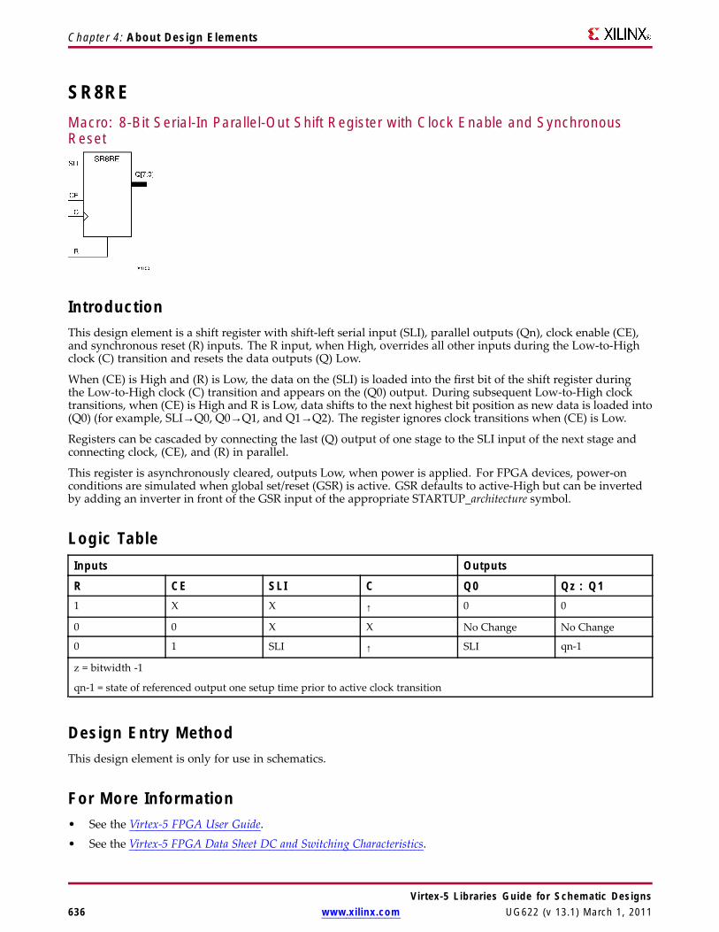
Chapter 4: About Design Elements
SR8REMacro: 8-Bit Serial-In Parallel-Out Shift Register with Clock Enable and SynchronousReset
IntroductionThis design element is a shift register with shift-left serial input (SLI), parallel outputs (Qn), clock enable (CE),and synchronous reset (R) inputs. The R input, when High, overrides all other inputs during the Low-to-Highclock (C) transition and resets the data outputs (Q) Low.
When (CE) is High and (R) is Low, the data on the (SLI) is loaded into the first bit of the shift register duringthe Low-to-High clock (C) transition and appears on the (Q0) output. During subsequent Low-to-High clocktransitions, when (CE) is High and R is Low, data shifts to the next highest bit position as new data is loaded into(Q0) (for example, SLI→Q0, Q0→Q1, and Q1→Q2). The register ignores clock transitions when (CE) is Low.
Registers can be cascaded by connecting the last (Q) output of one stage to the SLI input of the next stage andconnecting clock, (CE), and (R) in parallel.
This register is asynchronously cleared, outputs Low, when power is applied. For FPGA devices, power-onconditions are simulated when global set/reset (GSR) is active. GSR defaults to active-High but can be invertedby adding an inverter in front of the GSR input of the appropriate STARTUP_architecture symbol.
Logic TableInputs Outputs
R CE SLI C Q0 Qz : Q11 X X ↑ 0 0
0 0 X X No Change No Change
0 1 SLI ↑ SLI qn-1
z = bitwidth -1
qn-1 = state of referenced output one setup time prior to active clock transition
Design Entry MethodThis design element is only for use in schematics.
For More Information• See the Virtex-5 FPGA User Guide.• See the Virtex-5 FPGA Data Sheet DC and Switching Characteristics.
Virtex-5 Libraries Guide for Schematic Designs636 www.xilinx.com UG622 (v 13.1) March 1, 2011

Chapter 4: About Design Elements
SR8RLEMacro: 8-Bit Loadable Serial/Parallel-In Parallel-Out Shift Register with Clock Enableand Synchronous Reset
IntroductionThis design element is a shift register with shift-left serial input (SLI), parallel inputs (D), parallel outputs (Q),and three control inputs: clock enable (CE), load enable (L), and synchronous reset (R). The register ignores clocktransitions when (L) and (CE) are Low. The synchronous (R), when High, overrides all other inputs during theLow-to-High clock (C) transition and resets the data outputs (Q) Low. When (L) is High and (R) is Low duringthe Low-to-High clock transition, data on the (D) inputs is loaded into the corresponding Q bits of the register.
When (CE) is High and (L) and (R) are Low, data on the (SLI) input is loaded into the first bit of the shiftregister during the Low-to-High clock (C) transition and appears on the Q0 output. During subsequent clocktransitions, when (CE) is High and (L) and (R) are Low, the data shifts to the next highest bit position as newdata is loaded into Q0.
Registers can be cascaded by connecting the last Q output of one stage to the SLI input of the next stage andconnecting clock, (CE), (L), and (R) inputs in parallel.
This register is asynchronously cleared, outputs Low, when power is applied. For FPGA devices, power-onconditions are simulated when global set/reset (GSR) is active. GSR defaults to active-High but can be invertedby adding an inverter in front of the GSR input of the appropriate STARTUP_architecture symbol.
Logic TableInputs Outputs
R L CE SLI Dz : D0 C Q0 Qz : Q11 X X X X ↑ 0 0
0 1 X X Dz : D0 ↑ D0 Dn
0 0 1 SLI X ↑ SLI qn-1
0 0 0 X X X No Change No Change
z = bitwidth -1
qn-1 = state of referenced output one setup time prior to active clock transition
Design Entry MethodThis design element is only for use in schematics.
Virtex-5 Libraries Guide for Schematic DesignsUG622 (v 13.1) March 1, 2011 www.xilinx.com 637

Chapter 4: About Design Elements
For More Information• See the Virtex-5 FPGA User Guide.
• See the Virtex-5 FPGA Data Sheet DC and Switching Characteristics.
Virtex-5 Libraries Guide for Schematic Designs638 www.xilinx.com UG622 (v 13.1) March 1, 2011

Chapter 4: About Design Elements
SR8RLEDMacro: 8-Bit Shift Register with Clock Enable and Synchronous Reset
IntroductionThis design element is a shift register with shift-left (SLI) and shift-right (SRI) serial inputs, parallel inputs (D),parallel outputs (Q) and four control inputs — clock enable (CE), load enable (L), shift left/right (LEFT), andsynchronous reset (R). The register ignores clock transitions when (CE) and (L) are Low. The synchronous (R),when High, overrides all other inputs during the Low-to-High clock (C) transition and resets the data outputs(Q) Low. When (L) is High and (R) is Low during the Low-to-High clock transition, the data on the (D) inputs isloaded into the corresponding (Q) bits of the register.
When (CE) is High and (L) and (R) are Low, data shifts right or left, depending on the state of the LEFT input.If LEFT is High, data on (SLI) is loaded into (Q0) during the Low-to-High clock transition and shifted left (forexample, to Q1 and Q2) during subsequent clock transitions. If LEFT is Low, data on the (SRI) is loaded into thelast (Q) output during the Low-to-High clock transition and shifted right ) during subsequent clock transitions.The logic tables below indicates the state of the (Q) outputs under all input conditions.
This register is asynchronously cleared, outputs Low, when power is applied. For FPGA devices, power-onconditions are simulated when global set/reset (GSR) is active. GSR defaults to active-High but can be invertedby adding an inverter in front of the GSR input of the appropriate STARTUP_architecture symbol.
Logic TableInputs Outputs
R L CE LEFT SLI SRI D7 : D0 C Q0 Q7 Q6 : Q11 X X X X X X ↑ 0 0 0
0 1 X X X X D7 : D0 ↓ D0 D7 Dn
0 0 0 X X X X X NoChange
NoChange
NoChange
0 0 1 1 SLI X X ↑ SLI q6 qn-1
0 0 1 0 X SRI X ↓ q1 SRI qn+1
qn-1 or qn+1 = state of referenced output one setup time prior to active clock transition
Design Entry MethodThis design element is only for use in schematics.
Virtex-5 Libraries Guide for Schematic DesignsUG622 (v 13.1) March 1, 2011 www.xilinx.com 639

Chapter 4: About Design Elements
For More Information• See the Virtex-5 FPGA User Guide.
• See the Virtex-5 FPGA Data Sheet DC and Switching Characteristics.
Virtex-5 Libraries Guide for Schematic Designs640 www.xilinx.com UG622 (v 13.1) March 1, 2011
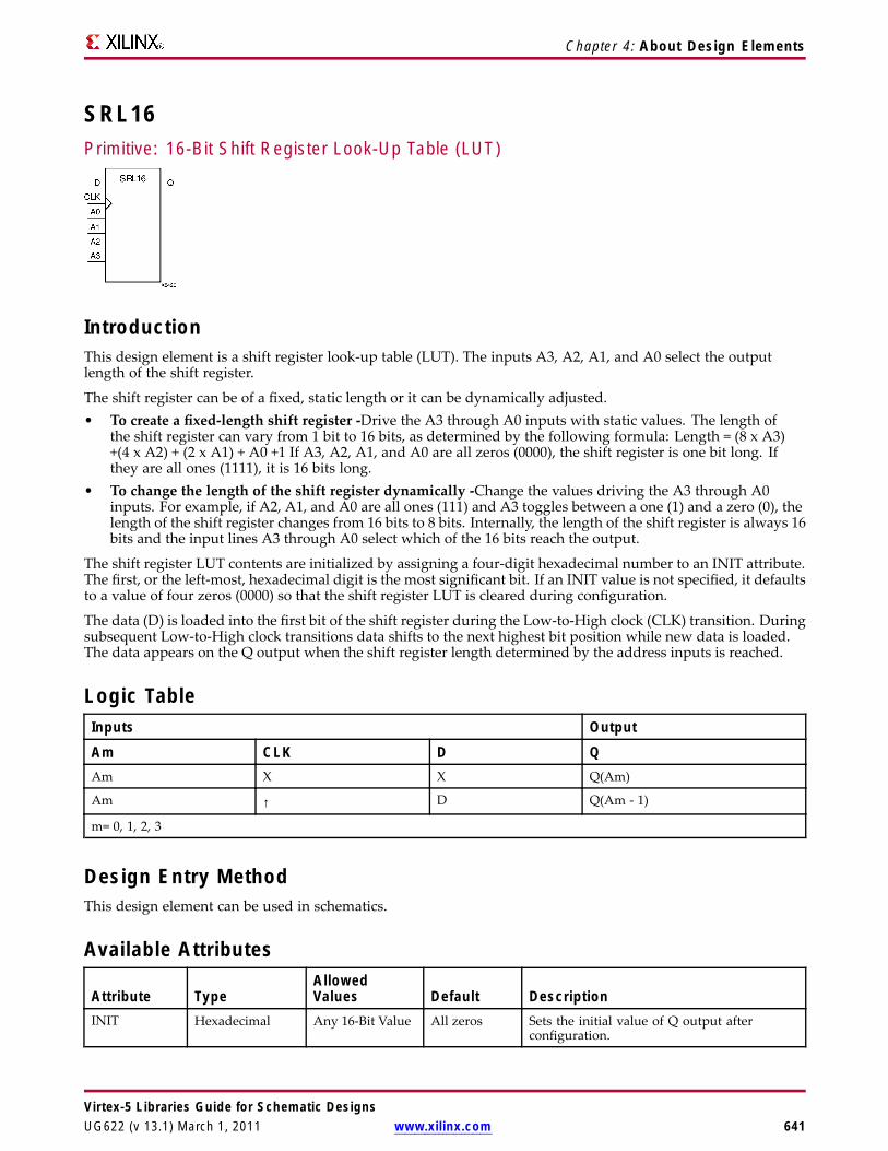
Chapter 4: About Design Elements
SRL16Primitive: 16-Bit Shift Register Look-Up Table (LUT)
IntroductionThis design element is a shift register look-up table (LUT). The inputs A3, A2, A1, and A0 select the outputlength of the shift register.
The shift register can be of a fixed, static length or it can be dynamically adjusted.• To create a fixed-length shift register -Drive the A3 through A0 inputs with static values. The length of
the shift register can vary from 1 bit to 16 bits, as determined by the following formula: Length = (8 x A3)+(4 x A2) + (2 x A1) + A0 +1 If A3, A2, A1, and A0 are all zeros (0000), the shift register is one bit long. Ifthey are all ones (1111), it is 16 bits long.
• To change the length of the shift register dynamically -Change the values driving the A3 through A0inputs. For example, if A2, A1, and A0 are all ones (111) and A3 toggles between a one (1) and a zero (0), thelength of the shift register changes from 16 bits to 8 bits. Internally, the length of the shift register is always 16bits and the input lines A3 through A0 select which of the 16 bits reach the output.
The shift register LUT contents are initialized by assigning a four-digit hexadecimal number to an INIT attribute.The first, or the left-most, hexadecimal digit is the most significant bit. If an INIT value is not specified, it defaultsto a value of four zeros (0000) so that the shift register LUT is cleared during configuration.
The data (D) is loaded into the first bit of the shift register during the Low-to-High clock (CLK) transition. Duringsubsequent Low-to-High clock transitions data shifts to the next highest bit position while new data is loaded.The data appears on the Q output when the shift register length determined by the address inputs is reached.
Logic TableInputs Output
Am CLK D QAm X X Q(Am)
Am ↑ D Q(Am - 1)
m= 0, 1, 2, 3
Design Entry MethodThis design element can be used in schematics.
Available Attributes
Attribute TypeAllowedValues Default Description
INIT Hexadecimal Any 16-Bit Value All zeros Sets the initial value of Q output afterconfiguration.
Virtex-5 Libraries Guide for Schematic DesignsUG622 (v 13.1) March 1, 2011 www.xilinx.com 641

Chapter 4: About Design Elements
For More Information• See the Virtex-5 FPGA User Guide.
• See the Virtex-5 FPGA Data Sheet DC and Switching Characteristics.
Virtex-5 Libraries Guide for Schematic Designs642 www.xilinx.com UG622 (v 13.1) March 1, 2011

Chapter 4: About Design Elements
SRL16_1Primitive: 16-Bit Shift Register Look-Up Table (LUT) with Negative-Edge Clock
IntroductionThis design element is a shift register look-up table (LUT). The inputs A3, A2, A1, and A0 select the outputlength of the shift register.
The shift register can be of a fixed, static length or it can be dynamically adjusted.• To create a fixed-length shift register -Drive the A3 through A0 inputs with static values. The length of
the shift register can vary from 1 bit to 16 bits, as determined by the following formula: Length = (8 x A3)+(4 x A2) + (2 x A1) + A0 +1 If A3, A2, A1, and A0 are all zeros (0000), the shift register is one bit long. Ifthey are all ones (1111), it is 16 bits long.
• To change the length of the shift register dynamically -Change the values driving the A3 through A0inputs. For example, if A2, A1, and A0 are all ones (111) and A3 toggles between a one (1) and a zero (0), thelength of the shift register changes from 16 bits to 8 bits. Internally, the length of the shift register is always 16bits and the input lines A3 through A0 select which of the 16 bits reach the output.
The shift register LUT contents are initialized by assigning a four-digit hexadecimal number to an INIT attribute.The first, or the left-most, hexadecimal digit is the most significant bit. If an INIT value is not specified, it defaultsto a value of four zeros (0000) so that the shift register LUT is cleared during configuration.
The data (D) is loaded into the first bit of the shift register during the High-to-Low clock (CLK) transition. Duringsubsequent High-to-Low clock transitions data shifts to the next highest bit position as new data is loaded. Thedata appears on the Q output when the shift register length determined by the address inputs is reached.
Logic TableInputs Output
Am CLK D QAm X X Q(Am)
Am ↓ D Q(Am - 1)
m= 0, 1, 2, 3
Design Entry MethodThis design element can be used in schematics.
Available AttributesAttribute Type Allowed Values Default DescriptionINIT Hexadecimal Any 16-Bit Value All zeros Sets the initial value of Q output after
configuration
Virtex-5 Libraries Guide for Schematic DesignsUG622 (v 13.1) March 1, 2011 www.xilinx.com 643

Chapter 4: About Design Elements
For More Information• See the Virtex-5 FPGA User Guide.
• See the Virtex-5 FPGA Data Sheet DC and Switching Characteristics.
Virtex-5 Libraries Guide for Schematic Designs644 www.xilinx.com UG622 (v 13.1) March 1, 2011

Chapter 4: About Design Elements
SRL16EPrimitive: 16-Bit Shift Register Look-Up Table (LUT) with Clock Enable
IntroductionThis design element is a shift register look-up table (LUT). The inputs A3, A2, A1, and A0 select the outputlength of the shift register.
The shift register can be of a fixed, static length or it can be dynamically adjusted.
• To create a fixed-length shift register -Drive the A3 through A0 inputs with static values. The length ofthe shift register can vary from 1 bit to 16 bits, as determined by the following formula: Length = (8 x A3)+(4 x A2) + (2 x A1) + A0 +1 If A3, A2, A1, and A0 are all zeros (0000), the shift register is one bit long. Ifthey are all ones (1111), it is 16 bits long.
• To change the length of the shift register dynamically -Change the values driving the A3 through A0inputs. For example, if A2, A1, and A0 are all ones (111) and A3 toggles between a one (1) and a zero (0), thelength of the shift register changes from 16 bits to 8 bits. Internally, the length of the shift register is always 16bits and the input lines A3 through A0 select which of the 16 bits reach the output.
The shift register LUT contents are initialized by assigning a four-digit hexadecimal number to an INIT attribute.The first, or the left-most, hexadecimal digit is the most significant bit. If an INIT value is not specified, it defaultsto a value of four zeros (0000) so that the shift register LUT is cleared during configuration.
When CE is High, the data (D) is loaded into the first bit of the shift register during the Low-to-High clock (CLK)transition. During subsequent Low-to-High clock transitions, when CE is High, data shifts to the next highest bitposition as new data is loaded. The data appears on the Q output when the shift register length determined bythe address inputs is reached. When CE is Low, the register ignores clock transitions.
Logic TableInputs Output
Am CE CLK D QAm 0 X X Q(Am)
Am 1 ↑ D Q(Am - 1)
m= 0, 1, 2, 3
Virtex-5 Libraries Guide for Schematic DesignsUG622 (v 13.1) March 1, 2011 www.xilinx.com 645
Chapter 4: About Design Elements
Port DescriptionsPort Direction Width FunctionQ Output 1 Shift register data output
D Input 1 Shift register data input
CLK Input 1 Clock
CE Input 1 Active high clock enable
A Input 4 Dynamic depth selection of the SRL
• A=0000 ==> 1-bit shift length
• A=1111 ==> 16-bit shift length
Design Entry MethodThis design element can be used in schematics.
Available AttributesAttribute Type Allowed Values Default DescriptionINIT Hexa-
decimalAny 16-Bit Value All zeros Sets the initial value of content and output of shift
register after configuration.
For More Information• See the Virtex-5 FPGA User Guide.
• See the Virtex-5 FPGA Data Sheet DC and Switching Characteristics.
Virtex-5 Libraries Guide for Schematic Designs646 www.xilinx.com UG622 (v 13.1) March 1, 2011

Chapter 4: About Design Elements
SRL16E_1Primitive: 16-Bit Shift Register Look-Up Table (LUT) with Negative-Edge Clock andClock Enable
IntroductionThis design element is a shift register look-up table (LUT) with clock enable (CE). The inputs A3, A2, A1,and A0 select the output length of the shift register.
The shift register can be of a fixed, static length or it can be dynamically adjusted.• To create a fixed-length shift register -Drive the A3 through A0 inputs with static values. The length of
the shift register can vary from 1 bit to 16 bits, as determined by the following formula: Length = (8 x A3)+(4 x A2) + (2 x A1) + A0 +1 If A3, A2, A1, and A0 are all zeros (0000), the shift register is one bit long. Ifthey are all ones (1111), it is 16 bits long.
• To change the length of the shift register dynamically -Change the values driving the A3 through A0inputs. For example, if A2, A1, and A0 are all ones (111) and A3 toggles between a one (1) and a zero (0), thelength of the shift register changes from 16 bits to 8 bits. Internally, the length of the shift register is always 16bits and the input lines A3 through A0 select which of the 16 bits reach the output.
The shift register LUT contents are initialized by assigning a four-digit hexadecimal number to an INIT attribute.The first, or the left-most, hexadecimal digit is the most significant bit. If an INIT value is not specified, it defaultsto a value of four zeros (0000) so that the shift register LUT is cleared during configuration.
When CE is High, the data (D) is loaded into the first bit of the shift register during the High-to-Low clock (CLK)transition. During subsequent High-to-Low clock transitions, when CE is High, data is shifted to the next highestbit position as new data is loaded. The data appears on the Q output when the shift register length determinedby the address inputs is reached. When CE is Low, the register ignores clock transitions.
Logic TableInputs Output
Am CE CLK D QAm 0 X X Q(Am)
Am 1 ↓ D Q(Am - 1)
m= 0, 1, 2, 3
Design Entry MethodThis design element can be used in schematics.
Available Attributes
Attribute TypeAllowedValues Default Description
INIT Hexadecimal Any 16-BitValue
All zeros Sets the initial value of content and output of shiftregister after configuration.
Virtex-5 Libraries Guide for Schematic DesignsUG622 (v 13.1) March 1, 2011 www.xilinx.com 647

Chapter 4: About Design Elements
For More Information• See the Virtex-5 FPGA User Guide.
• See the Virtex-5 FPGA Data Sheet DC and Switching Characteristics.
Virtex-5 Libraries Guide for Schematic Designs648 www.xilinx.com UG622 (v 13.1) March 1, 2011
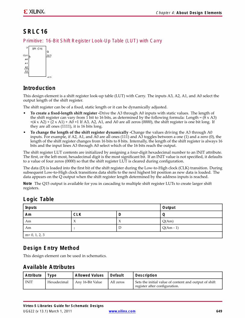
Chapter 4: About Design Elements
SRLC16Primitive: 16-Bit Shift Register Look-Up Table (LUT) with Carry
IntroductionThis design element is a shift register look-up table (LUT) with Carry. The inputs A3, A2, A1, and A0 select theoutput length of the shift register.
The shift register can be of a fixed, static length or it can be dynamically adjusted.• To create a fixed-length shift register -Drive the A3 through A0 inputs with static values. The length of
the shift register can vary from 1 bit to 16 bits, as determined by the following formula: Length = (8 x A3)+(4 x A2) + (2 x A1) + A0 +1 If A3, A2, A1, and A0 are all zeros (0000), the shift register is one bit long. Ifthey are all ones (1111), it is 16 bits long.
• To change the length of the shift register dynamically -Change the values driving the A3 through A0inputs. For example, if A2, A1, and A0 are all ones (111) and A3 toggles between a one (1) and a zero (0), thelength of the shift register changes from 16 bits to 8 bits. Internally, the length of the shift register is always 16bits and the input lines A3 through A0 select which of the 16 bits reach the output.
The shift register LUT contents are initialized by assigning a four-digit hexadecimal number to an INIT attribute.The first, or the left-most, hexadecimal digit is the most significant bit. If an INIT value is not specified, it defaultsto a value of four zeros (0000) so that the shift register LUT is cleared during configuration.
The data (D) is loaded into the first bit of the shift register during the Low-to-High clock (CLK) transition. Duringsubsequent Low-to-High clock transitions data shifts to the next highest bit position as new data is loaded. Thedata appears on the Q output when the shift register length determined by the address inputs is reached.
Note The Q15 output is available for you in cascading to multiple shift register LUTs to create larger shiftregisters.
Logic TableInputs Output
Am CLK D QAm X X Q(Am)
Am ↑ D Q(Am - 1)
m= 0, 1, 2, 3
Design Entry MethodThis design element can be used in schematics.
Available AttributesAttribute Type Allowed Values Default DescriptionINIT Hexadecimal Any 16-Bit Value All zeros Sets the initial value of content and output of shift
register after configuration.
Virtex-5 Libraries Guide for Schematic DesignsUG622 (v 13.1) March 1, 2011 www.xilinx.com 649

Chapter 4: About Design Elements
For More Information• See the Virtex-5 FPGA User Guide.
• See the Virtex-5 FPGA Data Sheet DC and Switching Characteristics.
Virtex-5 Libraries Guide for Schematic Designs650 www.xilinx.com UG622 (v 13.1) March 1, 2011
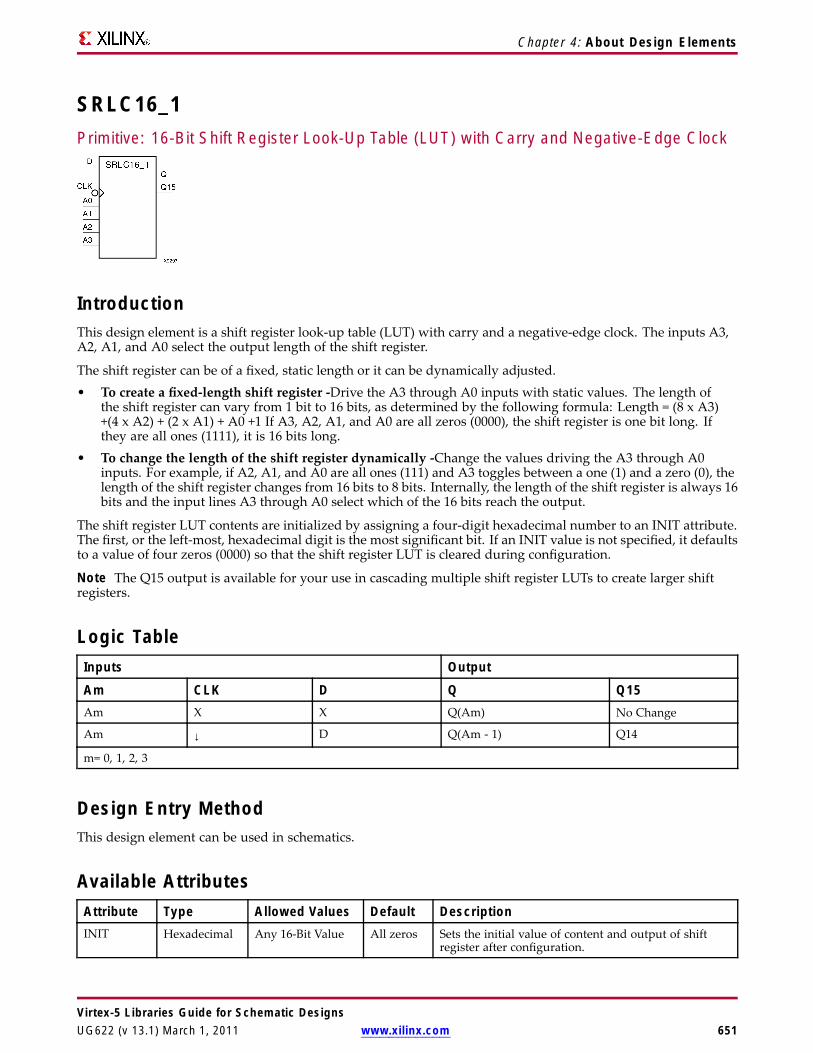
Chapter 4: About Design Elements
SRLC16_1Primitive: 16-Bit Shift Register Look-Up Table (LUT) with Carry and Negative-Edge Clock
IntroductionThis design element is a shift register look-up table (LUT) with carry and a negative-edge clock. The inputs A3,A2, A1, and A0 select the output length of the shift register.
The shift register can be of a fixed, static length or it can be dynamically adjusted.• To create a fixed-length shift register -Drive the A3 through A0 inputs with static values. The length of
the shift register can vary from 1 bit to 16 bits, as determined by the following formula: Length = (8 x A3)+(4 x A2) + (2 x A1) + A0 +1 If A3, A2, A1, and A0 are all zeros (0000), the shift register is one bit long. Ifthey are all ones (1111), it is 16 bits long.
• To change the length of the shift register dynamically -Change the values driving the A3 through A0inputs. For example, if A2, A1, and A0 are all ones (111) and A3 toggles between a one (1) and a zero (0), thelength of the shift register changes from 16 bits to 8 bits. Internally, the length of the shift register is always 16bits and the input lines A3 through A0 select which of the 16 bits reach the output.
The shift register LUT contents are initialized by assigning a four-digit hexadecimal number to an INIT attribute.The first, or the left-most, hexadecimal digit is the most significant bit. If an INIT value is not specified, it defaultsto a value of four zeros (0000) so that the shift register LUT is cleared during configuration.
Note The Q15 output is available for your use in cascading multiple shift register LUTs to create larger shiftregisters.
Logic TableInputs Output
Am CLK D Q Q15Am X X Q(Am) No Change
Am ↓ D Q(Am - 1) Q14
m= 0, 1, 2, 3
Design Entry MethodThis design element can be used in schematics.
Available AttributesAttribute Type Allowed Values Default DescriptionINIT Hexadecimal Any 16-Bit Value All zeros Sets the initial value of content and output of shift
register after configuration.
Virtex-5 Libraries Guide for Schematic DesignsUG622 (v 13.1) March 1, 2011 www.xilinx.com 651

Chapter 4: About Design Elements
For More Information• See the Virtex-5 FPGA User Guide.
• See the Virtex-5 FPGA Data Sheet DC and Switching Characteristics.
Virtex-5 Libraries Guide for Schematic Designs652 www.xilinx.com UG622 (v 13.1) March 1, 2011

Chapter 4: About Design Elements
SRLC16EPrimitive: 16-Bit Shift Register Look-Up Table (LUT) with Carry and Clock Enable
IntroductionThis design element is a shift register look-up table (LUT) with carry and clock enable. The inputs A3, A2, A1,and A0 select the output length of the shift register.
The shift register can be of a fixed, static length or it can be dynamically adjusted.
• To create a fixed-length shift register -Drive the A3 through A0 inputs with static values. The length ofthe shift register can vary from 1 bit to 16 bits, as determined by the following formula: Length = (8 x A3)+(4 x A2) + (2 x A1) + A0 +1 If A3, A2, A1, and A0 are all zeros (0000), the shift register is one bit long. Ifthey are all ones (1111), it is 16 bits long.
• To change the length of the shift register dynamically -Change the values driving the A3 through A0inputs. For example, if A2, A1, and A0 are all ones (111) and A3 toggles between a one (1) and a zero (0), thelength of the shift register changes from 16 bits to 8 bits. Internally, the length of the shift register is always 16bits and the input lines A3 through A0 select which of the 16 bits reach the output.
The shift register LUT contents are initialized by assigning a four-digit hexadecimal number to an INIT attribute.The first, or the left-most, hexadecimal digit is the most significant bit. If an INIT value is not specified, it defaultsto a value of four zeros (0000) so that the shift register LUT is cleared during configuration.
The data (D) is loaded into the first bit of the shift register during the Low-to-High clock (CLK) transition.When CE is High, during subsequent Low-to-High clock transitions, data shifts to the next highest bit positionas new data is loaded. The data appears on the Q output when the shift register length determined by theaddress inputs is reached.
Note The Q15 output is available for you in cascading to multiple shift register LUTs to create larger shiftregisters.
Logic TableInputs Output
Am CLK CE D Q Q15Am X 0 X Q(Am) Q(15)
Am X 1 X Q(Am) Q(15)
Am ↑ 1 D Q(Am - 1) Q15
m= 0, 1, 2, 3
Design Entry MethodThis design element can be used in schematics.
Virtex-5 Libraries Guide for Schematic DesignsUG622 (v 13.1) March 1, 2011 www.xilinx.com 653

Chapter 4: About Design Elements
Available AttributesAttribute Type Allowed Values Default DescriptionINIT Hexadecimal Any 16-Bit Value All zeros Sets the initial value of content and output of shift
register after configuration.
For More Information• See the Virtex-5 FPGA User Guide.
• See the Virtex-5 FPGA Data Sheet DC and Switching Characteristics.
Virtex-5 Libraries Guide for Schematic Designs654 www.xilinx.com UG622 (v 13.1) March 1, 2011

Chapter 4: About Design Elements
SRLC16E_1Primitive: 16-Bit Shift Register Look-Up Table (LUT) with Carry, Negative-Edge Clock,and Clock Enable
IntroductionThis design element is a shift register look-up table (LUT) with carry, clock enable, and negative-edge clock. Theinputs A3, A2, A1, and A0 select the output length of the shift register.
The shift register can be of a fixed, static length or it can be dynamically adjusted.• To create a fixed-length shift register -Drive the A3 through A0 inputs with static values. The length of
the shift register can vary from 1 bit to 16 bits, as determined by the following formula: Length = (8 x A3)+(4 x A2) + (2 x A1) + A0 +1 If A3, A2, A1, and A0 are all zeros (0000), the shift register is one bit long. Ifthey are all ones (1111), it is 16 bits long.
• To change the length of the shift register dynamically -Change the values driving the A3 through A0inputs. For example, if A2, A1, and A0 are all ones (111) and A3 toggles between a one (1) and a zero (0), thelength of the shift register changes from 16 bits to 8 bits. Internally, the length of the shift register is always 16bits and the input lines A3 through A0 select which of the 16 bits reach the output.
The shift register LUT contents are initialized by assigning a four-digit hexadecimal number to an INIT attribute.The first, or the left-most, hexadecimal digit is the most significant bit. If an INIT value is not specified, it defaultsto a value of four zeros (0000) so that the shift register LUT is cleared during configuration.
When CE is High, the data (D) is loaded into the first bit of the shift register during the High-to-Low clock (CLK)transition. During subsequent High-to-Low clock transitions data shifts to the next highest bit position as newdata is loaded when CE is High. The data appears on the Q output when the shift register length determined bythe address inputs is reached.
Note The Q15 output is available for your use in cascading multiple shift register LUTs to create larger shiftregisters.
Logic TableInputs Output
Am CE CLK D Q Q15Am 0 X X Q(Am) No Change
Am 1 X X Q(Am) No Change
Am 1 ↓ D Q(Am -1 ) Q14
m= 0, 1, 2, 3
Design Entry MethodThis design element can be used in schematics.
Virtex-5 Libraries Guide for Schematic DesignsUG622 (v 13.1) March 1, 2011 www.xilinx.com 655
Chapter 4: About Design Elements
Available Attributes
Attribute TypeAllowedValues Default Description
INIT Hexadecimal Any 16-BitValue
All zeros Sets the initial value of content and output of shift registerafter configuration.
For More Information• See the Virtex-5 FPGA User Guide.
• See the Virtex-5 FPGA Data Sheet DC and Switching Characteristics.
Virtex-5 Libraries Guide for Schematic Designs656 www.xilinx.com UG622 (v 13.1) March 1, 2011
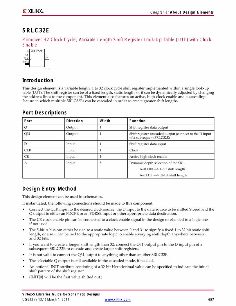
Chapter 4: About Design Elements
SRLC32EPrimitive: 32 Clock Cycle, Variable Length Shift Register Look-Up Table (LUT) with ClockEnable
IntroductionThis design element is a variable length, 1 to 32 clock cycle shift register implemented within a single look-uptable (LUT). The shift register can be of a fixed length, static length, or it can be dynamically adjusted by changingthe address lines to the component. This element also features an active, high-clock enable and a cascadingfeature in which multiple SRLC32Es can be cascaded in order to create greater shift lengths.
Port DescriptionsPort Direction Width FunctionQ Output 1 Shift register data output
Q31 Output 1 Shift register cascaded output (connect to the D inputof a subsequent SRLC32E)
D Input 1 Shift register data input
CLK Input 1 Clock
CE Input 1 Active high clock enable
A Input 5 Dynamic depth selection of the SRL
A=00000 ==> 1-bit shift length
A=11111 ==> 32-bit shift length
Design Entry MethodThis design element can be used in schematics.
If instantiated, the following connections should be made to this component:• Connect the CLK input to the desired clock source, the D input to the data source to be shifted/stored and the
Q output to either an FDCPE or an FDRSE input or other appropriate data destination.• The CE clock enable pin can be connected to a clock enable signal in the design or else tied to a logic one
if not used.• The 5-bit A bus can either be tied to a static value between 0 and 31 to signify a fixed 1 to 32 bit static shift
length, or else it can be tied to the appropriate logic to enable a varying shift depth anywhere between 1and 32 bits.
• If you want to create a longer shift length than 32, connect the Q31 output pin to the D input pin of asubsequent SRLC32E to cascade and create larger shift registers.
• It is not valid to connect the Q31 output to anything other than another SRLC32E.• The selectable Q output is still available in the cascaded mode, if needed.• An optional INIT attribute consisting of a 32-bit Hexadecimal value can be specified to indicate the initial
shift pattern of the shift register.• (INIT[0] will be the first value shifted out.)
Virtex-5 Libraries Guide for Schematic DesignsUG622 (v 13.1) March 1, 2011 www.xilinx.com 657
Chapter 4: About Design Elements
Available AttributesAttribute Type Allowed Values Default DescriptionINIT Hexa-
decimalAny 32-Bit Value All zeros Specifies the initial shift pattern of the
SRLC32E.
For More Information• See the Virtex-5 FPGA User Guide.
• See the Virtex-5 FPGA Data Sheet DC and Switching Characteristics.
Virtex-5 Libraries Guide for Schematic Designs658 www.xilinx.com UG622 (v 13.1) March 1, 2011
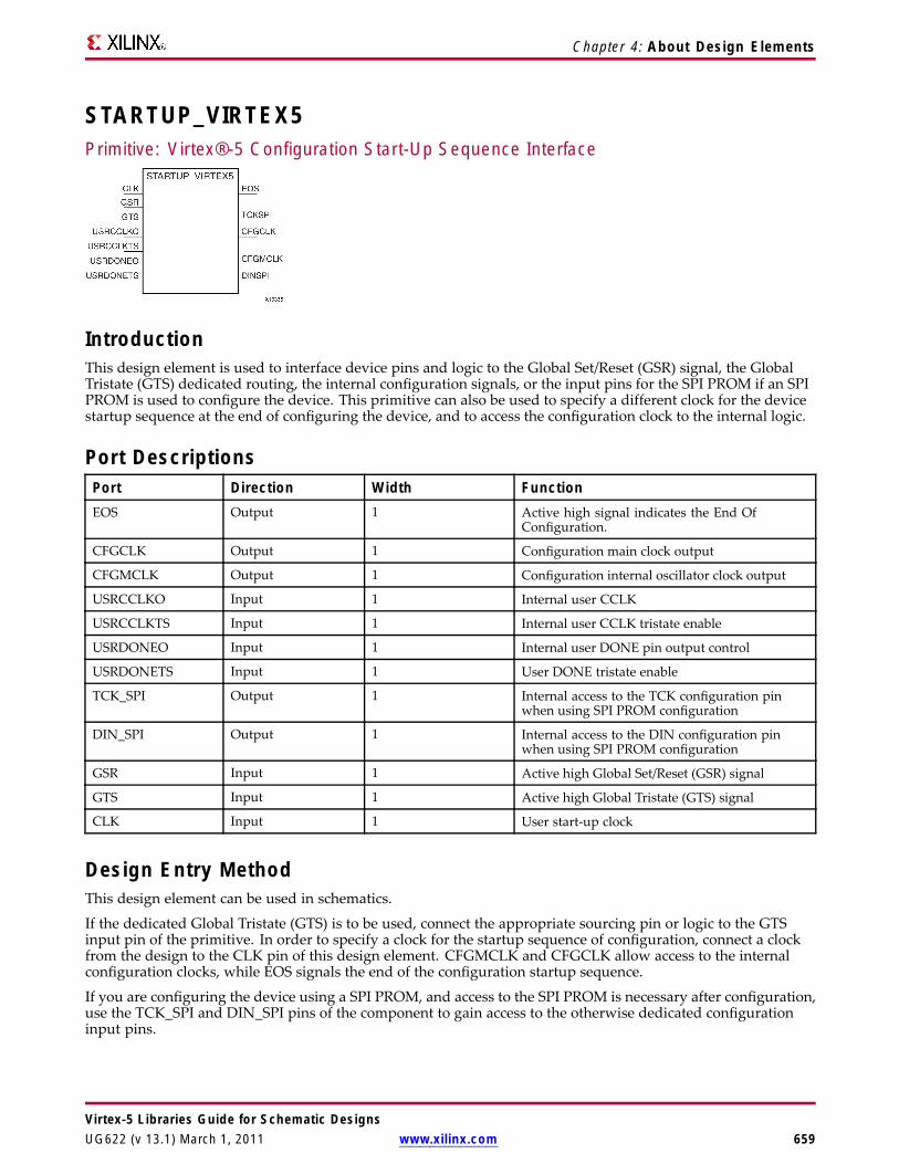
Chapter 4: About Design Elements
STARTUP_VIRTEX5Primitive: Virtex®-5 Configuration Start-Up Sequence Interface
IntroductionThis design element is used to interface device pins and logic to the Global Set/Reset (GSR) signal, the GlobalTristate (GTS) dedicated routing, the internal configuration signals, or the input pins for the SPI PROM if an SPIPROM is used to configure the device. This primitive can also be used to specify a different clock for the devicestartup sequence at the end of configuring the device, and to access the configuration clock to the internal logic.
Port DescriptionsPort Direction Width FunctionEOS Output 1 Active high signal indicates the End Of
Configuration.
CFGCLK Output 1 Configuration main clock output
CFGMCLK Output 1 Configuration internal oscillator clock output
USRCCLKO Input 1 Internal user CCLK
USRCCLKTS Input 1 Internal user CCLK tristate enable
USRDONEO Input 1 Internal user DONE pin output control
USRDONETS Input 1 User DONE tristate enable
TCK_SPI Output 1 Internal access to the TCK configuration pinwhen using SPI PROM configuration
DIN_SPI Output 1 Internal access to the DIN configuration pinwhen using SPI PROM configuration
GSR Input 1 Active high Global Set/Reset (GSR) signal
GTS Input 1 Active high Global Tristate (GTS) signal
CLK Input 1 User start-up clock
Design Entry MethodThis design element can be used in schematics.
If the dedicated Global Tristate (GTS) is to be used, connect the appropriate sourcing pin or logic to the GTSinput pin of the primitive. In order to specify a clock for the startup sequence of configuration, connect a clockfrom the design to the CLK pin of this design element. CFGMCLK and CFGCLK allow access to the internalconfiguration clocks, while EOS signals the end of the configuration startup sequence.
If you are configuring the device using a SPI PROM, and access to the SPI PROM is necessary after configuration,use the TCK_SPI and DIN_SPI pins of the component to gain access to the otherwise dedicated configurationinput pins.
Virtex-5 Libraries Guide for Schematic DesignsUG622 (v 13.1) March 1, 2011 www.xilinx.com 659

Chapter 4: About Design Elements
For More Information• See the Virtex-5 FPGA Configuration User Guide.
• See the Virtex-5 FPGA Data Sheet DC and Switching Characteristics.
• See the Virtex-5 FPGA User Guide.
Virtex-5 Libraries Guide for Schematic Designs660 www.xilinx.com UG622 (v 13.1) March 1, 2011

Chapter 4: About Design Elements
SYSMONPrimitive: System Monitor
IntroductionThis design element is built around a 10-bit, 200-kSPS (kilosamples per second) Analog-to-Digital Converter(ADC). When combined with a number of on-chip sensors, the ADC is used to measure FPGA physical operatingparameters, including on-chip power supply voltages and die temperatures. Access to external voltages isprovided through a dedicated analog-input pair (VP/VN) and 16 user-selectable analog inputs, known asauxiliary analog inputs (VAUXP[15:0], VAUXN[15:0]). The external analog inputs allow the ADC to monitorthe physical environment of the board or enclosure.
Virtex-5 Libraries Guide for Schematic DesignsUG622 (v 13.1) March 1, 2011 www.xilinx.com 661

Chapter 4: About Design Elements
Port DescriptionsPort Type Width FunctionALM[2:0] Output 3 3-bit output alarm for temp, Vccint and Vccaux
BUSY Output 1 1-bit output ADC busy signal
CHANNEL[4:0] Output 5 5-bit output channel selection
CONVST Input 1 1-bit input convert start
CONVSTCLK Input 1 1-bit input convert start clock
DADDR[6:0] Input 7 7-bit input address bus for dynamic reconfig
DCLK Input 1 1-bit input clock for dynamic reconfig
DEN Input 1 1-bit input enable for dynamic reconfig
DI[15:0] Input 16 16-bit input data bus for dynamic reconfig
DO[15:0] Output 16 16-bit output data bus for dynamic reconfig
DRDY Output 1 1-bit output data ready for dynamic reconfig
DWE Input 1 1-bit input write enable for dynamic reconfig
EOC Output 1 1-bit output end of conversion
EOS Output 1 1-bit output end of sequence
JTAGBUSY Output 1 1-bit output JTAG DRP busy
JTAGLOCKED Output 1 1-bit output DRP port lock
JTAGMODIFIED Output 1 1-bit output JTAG write to DRP
OT Output 1 1-bit output over temperature alarm
RESET Input 1 1-bit input active high reset
VAUXN[15:0] Input 16 16-bit input N-side auxiliary analog input
VAUXP[15:0] Input 16 16-bit input P-side auxiliary analog input
VN Input 1 1-bit input N-side analog input
VP Input 1 1-bit input P-side analog input
Design Entry MethodConnect all desired input and output ports and set the appropriate attributes for the desired behavior of thiscomponent. For simulation, provide a text file to give the analog and temperature to the model. The formatfor this file is as follows:
// Must use valid headers on all columns// Comments can be added to the stimulus file using ’//’TIME TEMP VCCAUX VCCINT VP VN VAUXP[0] VAUXN[0]00000 45 2.5 1.0 0.5 0.0 0.7 0.005000 85 2.45 1.1 0.3 0.0 0.2 0.0// Time stamp data is in nano seconds (ns)// Temperature is recorded in C (degrees centigrade)// All other channels are recorded as V (Volts)// Valid column headers are:// TIME, TEMP, VCCAUX, VCCINT, VP, VN,// VAUXP[0], VAUXN[0],...............VAUXP[15], VAUXN[15]// External analog inputs are differential so VP = 0.5 and VN = 0.0 the// input on channel VP/VN is 0.5 - 0.0 = 0.5V
Note When compiling the included code, please do not add any extraneous spaces to the text as this couldcause compilation to fail.
Virtex-5 Libraries Guide for Schematic Designs662 www.xilinx.com UG622 (v 13.1) March 1, 2011
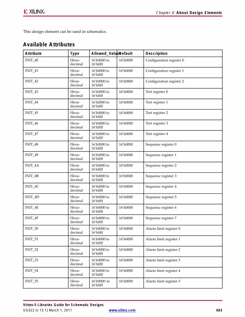
Chapter 4: About Design Elements
This design element can be used in schematics.
Available AttributesAttribute Type Allowed_ValuesDefault DescriptionINIT_40 Hexa-
decimal16’h0000 to16’hffff
16’h0000 Configuration register 0
INIT_41 Hexa-decimal
16’h0000 to16’hffff
16’h0000 Configuration register 1
INIT_42 Hexa-decimal
16’h0000 to16’hffff
16’h0800 Configuration register 2
INIT_43 Hexa-decimal
16’h0000 to16’hffff
16’h0000 Test register 0
INIT_44 Hexa-decimal
16’h0000 to16’hffff
16’h0000 Test register 1
INIT_45 Hexa-decimal
16’h0000 to16’hffff
16’h0000 Test register 2
INIT_46 Hexa-decimal
16’h0000 to16’hffff
16’h0000 Test register 3
INIT_47 Hexa-decimal
16’h0000 to16’hffff
16’h0000 Test register 4
INIT_48 Hexa-decimal
16’h0000 to16’hffff
16’h0000 Sequence register 0
INIT_49 Hexa-decimal
16’h0000 to16’hffff
16’h0000 Sequence register 1
INIT_4A Hexa-decimal
16’h0000 to16’hffff
16’h0000 Sequence register 2
INIT_4B Hexa-decimal
16’h0000 to16’hffff
16’h0000 Sequence register 3
INIT_4C Hexa-decimal
16’h0000 to16’hffff
16’h0000 Sequence register 4
INIT_4D Hexa-decimal
16’h0000 to16’hffff
16’h0000 Sequence register 5
INIT_4E Hexa-decimal
16’h0000 to16’hffff
16’h0000 Sequence register 6
INIT_4F Hexa-decimal
16’h0000 to16’hffff
16’h0000 Sequence register 7
INIT_50 Hexa-decimal
16’h0000 to16’hffff
16’h0000 Alarm limit register 0
INIT_51 Hexa-decimal
16’h0000 to16’hffff
16’h0000 Alarm limit register 1
INIT_52 Hexa-decimal
16’h0000 to16’hffff
16’h0000 Alarm limit register 2
INIT_53 Hexa-decimal
16’h0000 to16’hffff
16’h0000 Alarm limit register 3
INIT_54 Hexa-decimal
16’h0000 to16’hffff
16’h0000 Alarm limit register 4
INIT_55 Hexa-decimal
16’h0000 to16’hffff
16’h0000 Alarm limit register 5
Virtex-5 Libraries Guide for Schematic DesignsUG622 (v 13.1) March 1, 2011 www.xilinx.com 663
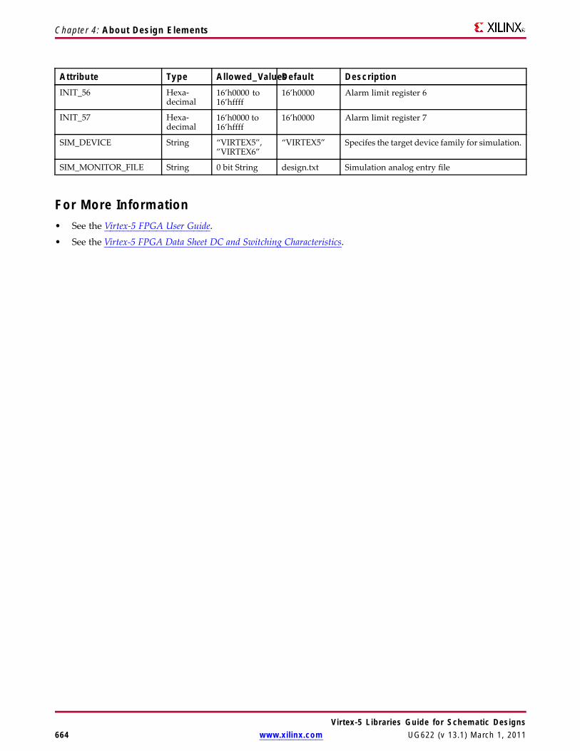
Chapter 4: About Design Elements
Attribute Type Allowed_ValuesDefault DescriptionINIT_56 Hexa-
decimal16’h0000 to16’hffff
16’h0000 Alarm limit register 6
INIT_57 Hexa-decimal
16’h0000 to16’hffff
16’h0000 Alarm limit register 7
SIM_DEVICE String “VIRTEX5”,”VIRTEX6”
“VIRTEX5” Specifes the target device family for simulation.
SIM_MONITOR_FILE String 0 bit String design.txt Simulation analog entry file
For More Information• See the Virtex-5 FPGA User Guide.
• See the Virtex-5 FPGA Data Sheet DC and Switching Characteristics.
Virtex-5 Libraries Guide for Schematic Designs664 www.xilinx.com UG622 (v 13.1) March 1, 2011
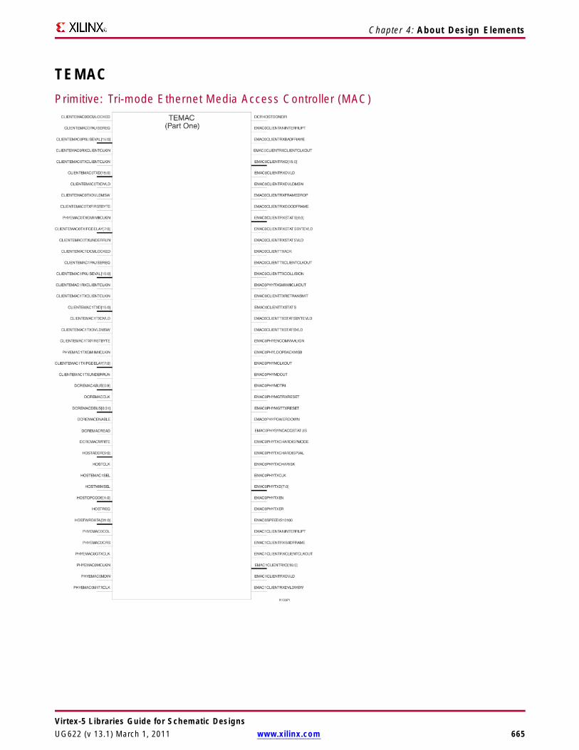
Chapter 4: About Design Elements
TEMACPrimitive: Tri-mode Ethernet Media Access Controller (MAC)
Virtex-5 Libraries Guide for Schematic DesignsUG622 (v 13.1) March 1, 2011 www.xilinx.com 665

Chapter 4: About Design Elements
IntroductionThis design element contains paired embedded Ethernet MACs that are independently configurable to meet allcommon Ethernet system connectivity needs.
Design Entry MethodThis design element can be used in schematics.
Virtex-5 Libraries Guide for Schematic Designs666 www.xilinx.com UG622 (v 13.1) March 1, 2011

Chapter 4: About Design Elements
For More Information• See the Virtex-5 Embedded Tri-Mode Ethernet MAC User Guide.
• See the Virtex-5 FPGA Data Sheet DC and Switching Characteristics.
• See the Virtex-5 FPGA User Guide.
Virtex-5 Libraries Guide for Schematic DesignsUG622 (v 13.1) March 1, 2011 www.xilinx.com 667
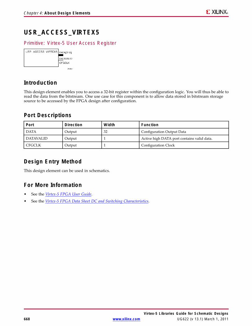
Chapter 4: About Design Elements
USR_ACCESS_VIRTEX5Primitive: Virtex-5 User Access Register
IntroductionThis design element enables you to access a 32-bit register within the configuration logic. You will thus be able toread the data from the bitstream. One use case for this component is to allow data stored in bitstream storagesource to be accessed by the FPGA design after configuration.
Port DescriptionsPort Direction Width FunctionDATA Output 32 Configuration Output Data
DATAVALID Output 1 Active high DATA port contains valid data.
CFGCLK Output 1 Configuration Clock
Design Entry MethodThis design element can be used in schematics.
For More Information• See the Virtex-5 FPGA User Guide.
• See the Virtex-5 FPGA Data Sheet DC and Switching Characteristics.
Virtex-5 Libraries Guide for Schematic Designs668 www.xilinx.com UG622 (v 13.1) March 1, 2011
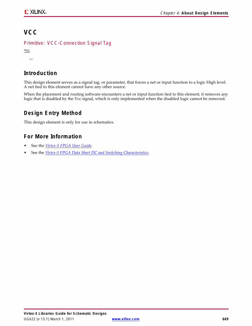
Chapter 4: About Design Elements
VCCPrimitive: VCC-Connection Signal Tag
IntroductionThis design element serves as a signal tag, or parameter, that forces a net or input function to a logic High level.A net tied to this element cannot have any other source.
When the placement and routing software encounters a net or input function tied to this element, it removes anylogic that is disabled by the Vcc signal, which is only implemented when the disabled logic cannot be removed.
Design Entry MethodThis design element is only for use in schematics.
For More Information• See the Virtex-5 FPGA User Guide.
• See the Virtex-5 FPGA Data Sheet DC and Switching Characteristics.
Virtex-5 Libraries Guide for Schematic DesignsUG622 (v 13.1) March 1, 2011 www.xilinx.com 669
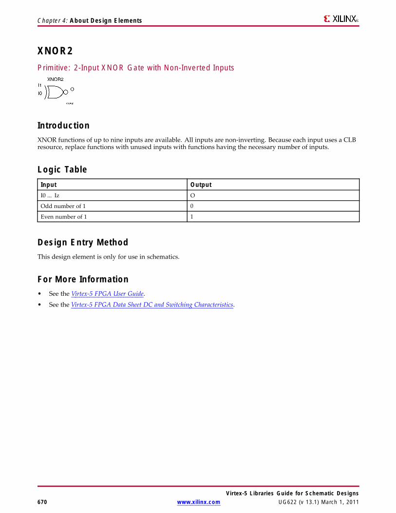
Chapter 4: About Design Elements
XNOR2Primitive: 2-Input XNOR Gate with Non-Inverted Inputs
IntroductionXNOR functions of up to nine inputs are available. All inputs are non-inverting. Because each input uses a CLBresource, replace functions with unused inputs with functions having the necessary number of inputs.
Logic TableInput OutputI0 ... Iz O
Odd number of 1 0
Even number of 1 1
Design Entry MethodThis design element is only for use in schematics.
For More Information• See the Virtex-5 FPGA User Guide.
• See the Virtex-5 FPGA Data Sheet DC and Switching Characteristics.
Virtex-5 Libraries Guide for Schematic Designs670 www.xilinx.com UG622 (v 13.1) March 1, 2011

Chapter 4: About Design Elements
XNOR3Primitive: 3-Input XNOR Gate with Non-Inverted Inputs
IntroductionXNOR functions of up to nine inputs are available. All inputs are non-inverting. Because each input uses a CLBresource, replace functions with unused inputs with functions having the necessary number of inputs.
Logic TableInput OutputI0 ... Iz O
Odd number of 1 0
Even number of 1 1
Design Entry MethodThis design element is only for use in schematics.
For More Information• See the Virtex-5 FPGA User Guide.
• See the Virtex-5 FPGA Data Sheet DC and Switching Characteristics.
Virtex-5 Libraries Guide for Schematic DesignsUG622 (v 13.1) March 1, 2011 www.xilinx.com 671
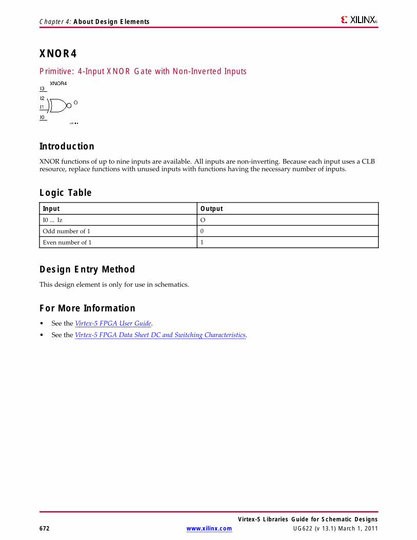
Chapter 4: About Design Elements
XNOR4Primitive: 4-Input XNOR Gate with Non-Inverted Inputs
IntroductionXNOR functions of up to nine inputs are available. All inputs are non-inverting. Because each input uses a CLBresource, replace functions with unused inputs with functions having the necessary number of inputs.
Logic TableInput OutputI0 ... Iz O
Odd number of 1 0
Even number of 1 1
Design Entry MethodThis design element is only for use in schematics.
For More Information• See the Virtex-5 FPGA User Guide.
• See the Virtex-5 FPGA Data Sheet DC and Switching Characteristics.
Virtex-5 Libraries Guide for Schematic Designs672 www.xilinx.com UG622 (v 13.1) March 1, 2011
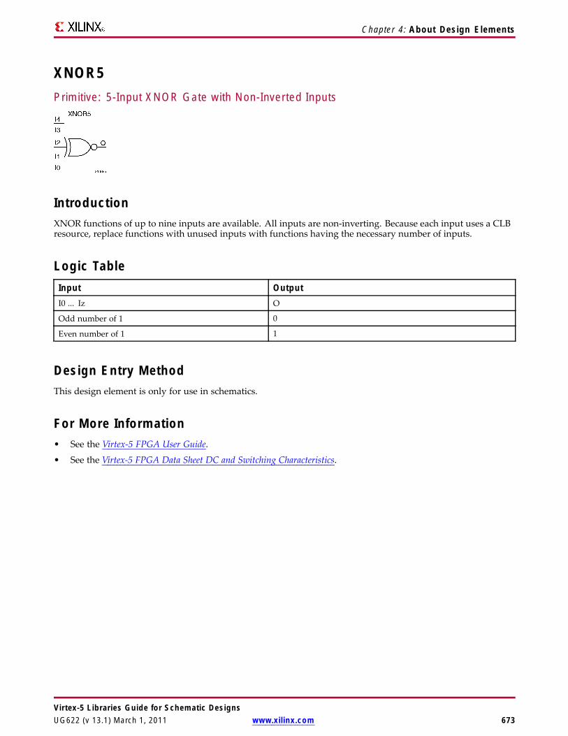
Chapter 4: About Design Elements
XNOR5Primitive: 5-Input XNOR Gate with Non-Inverted Inputs
IntroductionXNOR functions of up to nine inputs are available. All inputs are non-inverting. Because each input uses a CLBresource, replace functions with unused inputs with functions having the necessary number of inputs.
Logic TableInput OutputI0 ... Iz O
Odd number of 1 0
Even number of 1 1
Design Entry MethodThis design element is only for use in schematics.
For More Information• See the Virtex-5 FPGA User Guide.
• See the Virtex-5 FPGA Data Sheet DC and Switching Characteristics.
Virtex-5 Libraries Guide for Schematic DesignsUG622 (v 13.1) March 1, 2011 www.xilinx.com 673

Chapter 4: About Design Elements
XNOR6Macro: 6-Input XNOR Gate with Non-Inverted Inputs
IntroductionXNOR functions of up to nine inputs are available. All inputs are non-inverting. Because each input uses a CLBresource, replace functions with unused inputs with functions having the necessary number of inputs.
Logic TableInput OutputI0 ... Iz O
Odd number of 1 0
Even number of 1 1
Design Entry MethodThis design element is only for use in schematics.
For More Information• See the Virtex-5 FPGA User Guide.
• See the Virtex-5 FPGA Data Sheet DC and Switching Characteristics.
Virtex-5 Libraries Guide for Schematic Designs674 www.xilinx.com UG622 (v 13.1) March 1, 2011
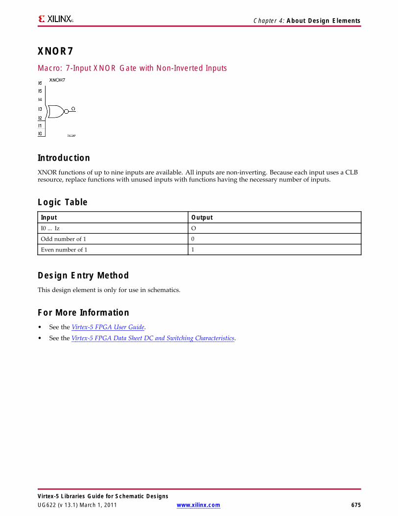
Chapter 4: About Design Elements
XNOR7Macro: 7-Input XNOR Gate with Non-Inverted Inputs
IntroductionXNOR functions of up to nine inputs are available. All inputs are non-inverting. Because each input uses a CLBresource, replace functions with unused inputs with functions having the necessary number of inputs.
Logic TableInput OutputI0 ... Iz O
Odd number of 1 0
Even number of 1 1
Design Entry MethodThis design element is only for use in schematics.
For More Information• See the Virtex-5 FPGA User Guide.
• See the Virtex-5 FPGA Data Sheet DC and Switching Characteristics.
Virtex-5 Libraries Guide for Schematic DesignsUG622 (v 13.1) March 1, 2011 www.xilinx.com 675

Chapter 4: About Design Elements
XNOR8Macro: 8-Input XNOR Gate with Non-Inverted Inputs
IntroductionXNOR functions of up to nine inputs are available. All inputs are non-inverting. Because each input uses a CLBresource, replace functions with unused inputs with functions having the necessary number of inputs.
Logic TableInput OutputI0 ... Iz O
Odd number of 1 0
Even number of 1 1
Design Entry MethodThis design element is only for use in schematics.
For More Information• See the Virtex-5 FPGA User Guide.
• See the Virtex-5 FPGA Data Sheet DC and Switching Characteristics.
Virtex-5 Libraries Guide for Schematic Designs676 www.xilinx.com UG622 (v 13.1) March 1, 2011

Chapter 4: About Design Elements
XNOR9Macro: 9-Input XNOR Gate with Non-Inverted Inputs
IntroductionXNOR functions of up to nine inputs are available. All inputs are non-inverting. Because each input uses a CLBresource, replace functions with unused inputs with functions having the necessary number of inputs.
Logic TableInput OutputI0 ... Iz O
Odd number of 1 0
Even number of 1 1
Design Entry MethodThis design element is only for use in schematics.
For More Information• See the Virtex-5 FPGA User Guide.
• See the Virtex-5 FPGA Data Sheet DC and Switching Characteristics.
Virtex-5 Libraries Guide for Schematic DesignsUG622 (v 13.1) March 1, 2011 www.xilinx.com 677

Chapter 4: About Design Elements
XOR2Primitive: 2-Input XOR Gate with Non-Inverted Inputs
IntroductionXOR functions of up to nine inputs are available. All inputs are non-inverting. Because each input uses a CLBresource, replace functions with unused inputs with functions having the necessary number of inputs.
Design Entry MethodThis design element is only for use in schematics.
For More Information• See the Virtex-5 FPGA User Guide.
• See the Virtex-5 FPGA Data Sheet DC and Switching Characteristics.
Virtex-5 Libraries Guide for Schematic Designs678 www.xilinx.com UG622 (v 13.1) March 1, 2011
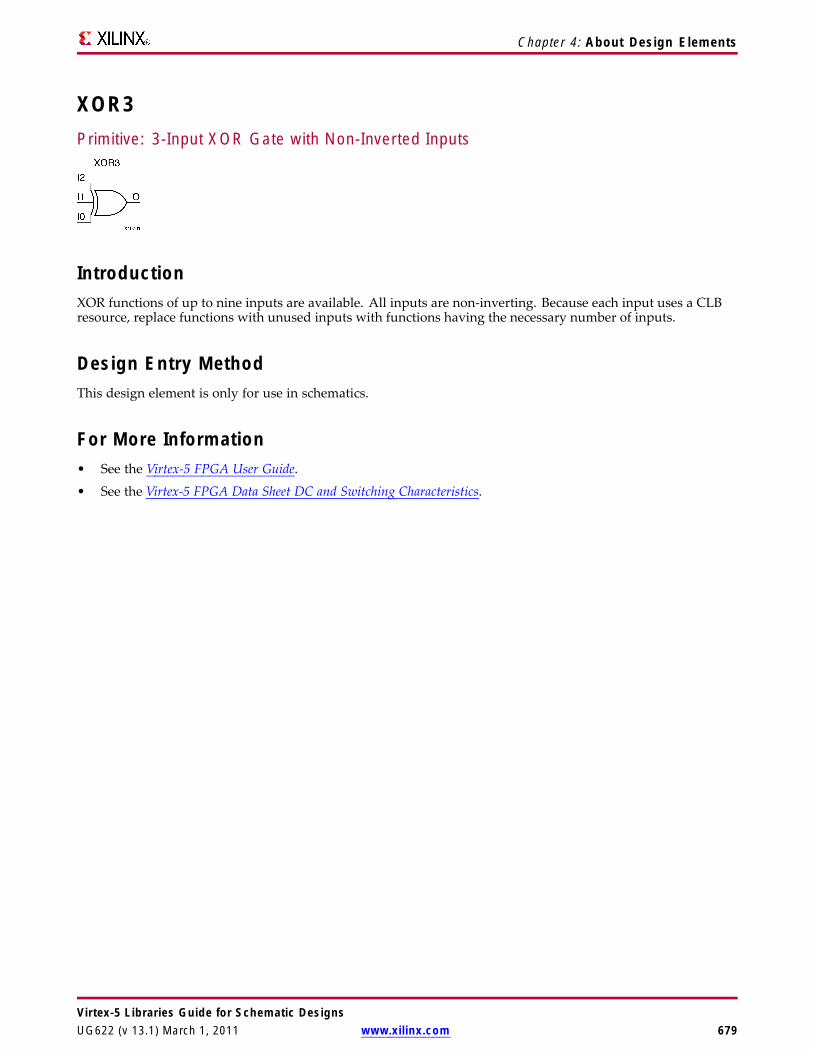
Chapter 4: About Design Elements
XOR3Primitive: 3-Input XOR Gate with Non-Inverted Inputs
IntroductionXOR functions of up to nine inputs are available. All inputs are non-inverting. Because each input uses a CLBresource, replace functions with unused inputs with functions having the necessary number of inputs.
Design Entry MethodThis design element is only for use in schematics.
For More Information• See the Virtex-5 FPGA User Guide.
• See the Virtex-5 FPGA Data Sheet DC and Switching Characteristics.
Virtex-5 Libraries Guide for Schematic DesignsUG622 (v 13.1) March 1, 2011 www.xilinx.com 679

Chapter 4: About Design Elements
XOR4Primitive: 4-Input XOR Gate with Non-Inverted Inputs
IntroductionXOR functions of up to nine inputs are available. All inputs are non-inverting. Because each input uses a CLBresource, replace functions with unused inputs with functions having the necessary number of inputs.
Design Entry MethodThis design element is only for use in schematics.
For More Information• See the Virtex-5 FPGA User Guide.
• See the Virtex-5 FPGA Data Sheet DC and Switching Characteristics.
Virtex-5 Libraries Guide for Schematic Designs680 www.xilinx.com UG622 (v 13.1) March 1, 2011

Chapter 4: About Design Elements
XOR5Primitive: 5-Input XOR Gate with Non-Inverted Inputs
IntroductionXOR functions of up to nine inputs are available. All inputs are non-inverting. Because each input uses a CLBresource, replace functions with unused inputs with functions having the necessary number of inputs.
Design Entry MethodThis design element is only for use in schematics.
For More Information• See the Virtex-5 FPGA User Guide.
• See the Virtex-5 FPGA Data Sheet DC and Switching Characteristics.
Virtex-5 Libraries Guide for Schematic DesignsUG622 (v 13.1) March 1, 2011 www.xilinx.com 681
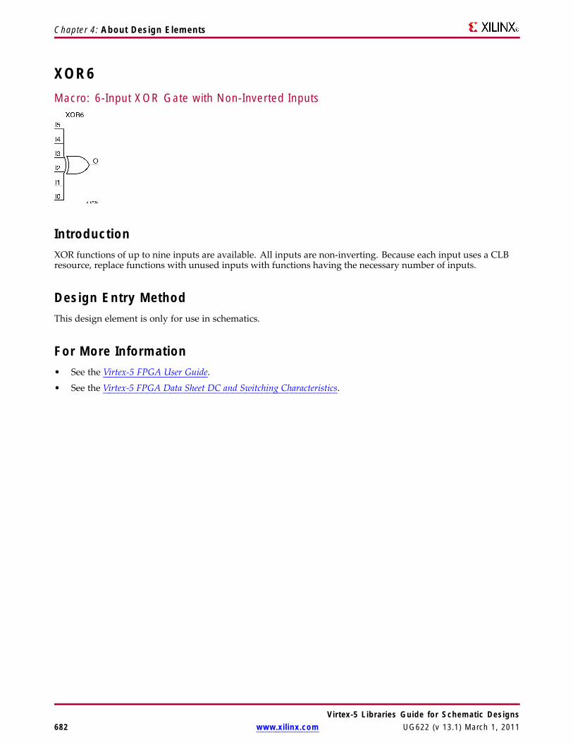
Chapter 4: About Design Elements
XOR6Macro: 6-Input XOR Gate with Non-Inverted Inputs
IntroductionXOR functions of up to nine inputs are available. All inputs are non-inverting. Because each input uses a CLBresource, replace functions with unused inputs with functions having the necessary number of inputs.
Design Entry MethodThis design element is only for use in schematics.
For More Information• See the Virtex-5 FPGA User Guide.
• See the Virtex-5 FPGA Data Sheet DC and Switching Characteristics.
Virtex-5 Libraries Guide for Schematic Designs682 www.xilinx.com UG622 (v 13.1) March 1, 2011
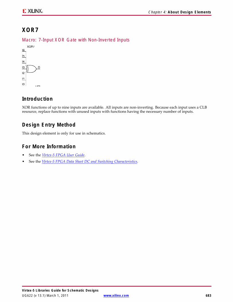
Chapter 4: About Design Elements
XOR7Macro: 7-Input XOR Gate with Non-Inverted Inputs
IntroductionXOR functions of up to nine inputs are available. All inputs are non-inverting. Because each input uses a CLBresource, replace functions with unused inputs with functions having the necessary number of inputs.
Design Entry MethodThis design element is only for use in schematics.
For More Information• See the Virtex-5 FPGA User Guide.
• See the Virtex-5 FPGA Data Sheet DC and Switching Characteristics.
Virtex-5 Libraries Guide for Schematic DesignsUG622 (v 13.1) March 1, 2011 www.xilinx.com 683

Chapter 4: About Design Elements
XOR8Macro: 8-Input XOR Gate with Non-Inverted Inputs
IntroductionXOR functions of up to nine inputs are available. All inputs are non-inverting. Because each input uses a CLBresource, replace functions with unused inputs with functions having the necessary number of inputs.
Design Entry MethodThis design element is only for use in schematics.
For More Information• See the Virtex-5 FPGA User Guide.
• See the Virtex-5 FPGA Data Sheet DC and Switching Characteristics.
Virtex-5 Libraries Guide for Schematic Designs684 www.xilinx.com UG622 (v 13.1) March 1, 2011

Chapter 4: About Design Elements
XOR9Macro: 9-Input XOR Gate with Non-Inverted Inputs
IntroductionXOR functions of up to nine inputs are available. All inputs are non-inverting. Because each input uses a CLBresource, replace functions with unused inputs with functions having the necessary number of inputs.
Design Entry MethodThis design element is only for use in schematics.
For More Information• See the Virtex-5 FPGA User Guide.
• See the Virtex-5 FPGA Data Sheet DC and Switching Characteristics.
Virtex-5 Libraries Guide for Schematic DesignsUG622 (v 13.1) March 1, 2011 www.xilinx.com 685

Chapter 4: About Design Elements
XORCYPrimitive: XOR for Carry Logic with General Output
IntroductionThis design element is a special XOR with general O output that generates faster and smaller arithmeticfunctions. The XORCY primitive is a dedicated XOR function within the carry-chain logic of the slice. It allowsfor fast and efficient creation of arithmetic (add/subtract) or wide logic functions (large AND/OR gate).
Logic TableInput Output
LI CI O0 0 0
0 1 1
1 0 1
1 1 0
Design Entry MethodThis design element can be used in schematics.
For More Information• See the Virtex-5 FPGA User Guide.
• See the Virtex-5 FPGA Data Sheet DC and Switching Characteristics.
Virtex-5 Libraries Guide for Schematic Designs686 www.xilinx.com UG622 (v 13.1) March 1, 2011