Xilinx Virtex-4 Libraries Guide for HDL Designs -...
323
Virtex-4 Libraries Guide for HDL Designs ISE 10.1
Transcript of Xilinx Virtex-4 Libraries Guide for HDL Designs -...

Vir tex-4 Libraries Guide for HDLDesigns
ISE 10.1

Xilinx Trademarks and Copyright Information
Xilinx is disclosing this user guide, manual, release note, and/or specification (the “Documentation”) to yousolely for use in the development of designs to operate with Xilinx hardware devices. You may not reproduce,distribute, republish, download, display, post, or transmit the Documentation in any form or by any meansincluding, but not limited to, electronic, mechanical, photocopying, recording, or otherwise, without the priorwritten consent of Xilinx. Xilinx expressly disclaims any liability arising out of your use of the Documentation.Xilinx reserves the right, at its sole discretion, to change the Documentation without notice at any time. Xilinxassumes no obligation to correct any errors contained in the Documentation, or to advise you of any correctionsor updates. Xilinx expressly disclaims any liability in connection with technical support or assistance that may beprovided to you in connection with the Information.
THE DOCUMENTATION IS DISCLOSED TO YOU “AS-IS” WITH NOWARRANTY OF ANY KIND. XILINXMAKES NO OTHER WARRANTIES, WHETHER EXPRESS, IMPLIED, OR STATUTORY, REGARDINGTHE DOCUMENTATION, INCLUDING ANY WARRANTIES OF MERCHANTABILITY, FITNESS FOR APARTICULAR PURPOSE, OR NONINFRINGEMENT OF THIRD-PARTY RIGHTS. IN NO EVENT WILLXILINX BE LIABLE FOR ANY CONSEQUENTIAL, INDIRECT, EXEMPLARY, SPECIAL, OR INCIDENTALDAMAGES, INCLUDING ANY LOSS OF DATA OR LOST PROFITS, ARISING FROM YOUR USE OF THEDOCUMENTATION.
© Copyright 2002 – 2008 Xilinx, Inc. All Rights Reserved. XILINX, the Xilinx logo, the Brand Window and otherdesignated brands included herein are trademarks of Xilinx, Inc. All other trademarks are the property of theirrespective owners. The PowerPC name and logo are registered trademarks of IBM Corp., and used under license.All other trademarks are the property of their respective owners.
Vir tex-4 Libraries Guide for HDL Designs
2 www.xilinx.com ISE 10.1
Table of ContentsAbout this Guide .......................................................................................................................................... 7Functional Categories ................................................................................................................................... 9About Design Elements............................................................................................................................... 15
BSCAN_VIRTEX4 ................................................................................................................................ 16BUFCF ................................................................................................................................................ 18BUFG.................................................................................................................................................. 20BUFGCE ............................................................................................................................................. 22BUFGCE_1 .......................................................................................................................................... 24BUFGCTRL ......................................................................................................................................... 26BUFGMUX.......................................................................................................................................... 28BUFGMUX_1....................................................................................................................................... 30BUFGMUX_VIRTEX4 .......................................................................................................................... 32BUFIO................................................................................................................................................. 34BUFR .................................................................................................................................................. 36CAPTURE_VIRTEX4............................................................................................................................ 38DCIRESET........................................................................................................................................... 40DCM_ADV ......................................................................................................................................... 42DCM_BASE......................................................................................................................................... 49DCM_PS ............................................................................................................................................. 55DSP48 ................................................................................................................................................. 63EMAC................................................................................................................................................. 70FDCE .................................................................................................................................................. 74FDCE_1............................................................................................................................................... 76FDCPE ................................................................................................................................................ 78FDCPE_1............................................................................................................................................. 81FDRSE ................................................................................................................................................ 83FDRSE_1 ............................................................................................................................................. 85FIFO16 ................................................................................................................................................ 87FRAME_ECC_VIRTEX4 ....................................................................................................................... 91GT11_CUSTOM................................................................................................................................... 93GT11_DUAL ....................................................................................................................................... 96GT11CLK ........................................................................................................................................... 101GT11CLK_MGT.................................................................................................................................. 102IBUF .................................................................................................................................................. 103IBUFDS.............................................................................................................................................. 106IBUFG................................................................................................................................................ 108IBUFGDS ........................................................................................................................................... 110ICAP_VIRTEX4 .................................................................................................................................. 113IDDR ................................................................................................................................................. 115IDELAY.............................................................................................................................................. 118IDELAYCTRL..................................................................................................................................... 122IOBUF................................................................................................................................................ 124IOBUFDS ........................................................................................................................................... 126ISERDES ............................................................................................................................................ 128KEEPER ............................................................................................................................................. 135LDCPE............................................................................................................................................... 137LUT1 ................................................................................................................................................. 140LUT1_D ............................................................................................................................................. 142LUT1_L.............................................................................................................................................. 145LUT2 ................................................................................................................................................. 148LUT2_D ............................................................................................................................................. 150LUT2_L.............................................................................................................................................. 153LUT3 ................................................................................................................................................. 155LUT3_D ............................................................................................................................................. 157LUT3_L.............................................................................................................................................. 159LUT4 ................................................................................................................................................. 161
Vir tex-4 Libraries Guide for HDL Designs
ISE 10.1 www.xilinx.com 3
LUT4_D ............................................................................................................................................. 164LUT4_L.............................................................................................................................................. 167MULT_AND....................................................................................................................................... 170MULT18X18 ....................................................................................................................................... 172MULT18X18S...................................................................................................................................... 174MUXCY ............................................................................................................................................. 176MUXCY_D ......................................................................................................................................... 178MUXCY_L.......................................................................................................................................... 180MUXF5 .............................................................................................................................................. 182MUXF5_D .......................................................................................................................................... 184MUXF5_L........................................................................................................................................... 186MUXF6 .............................................................................................................................................. 188MUXF6_D .......................................................................................................................................... 190MUXF6_L........................................................................................................................................... 192MUXF7 .............................................................................................................................................. 194MUXF7_D .......................................................................................................................................... 196MUXF7_L........................................................................................................................................... 198MUXF8 .............................................................................................................................................. 200MUXF8_D .......................................................................................................................................... 202MUXF8_L........................................................................................................................................... 204OBUF................................................................................................................................................. 206OBUFDS ............................................................................................................................................ 208OBUFT............................................................................................................................................... 210OBUFTDS .......................................................................................................................................... 212ODDR................................................................................................................................................ 214OSERDES........................................................................................................................................... 217PMCD................................................................................................................................................ 222PPC405_ADV ..................................................................................................................................... 225PULLDOWN...................................................................................................................................... 229PULLUP............................................................................................................................................. 231RAM16X1D ........................................................................................................................................ 233RAM16X1D_1..................................................................................................................................... 236RAM16X1S......................................................................................................................................... 239RAM16X1S_1...................................................................................................................................... 241RAM16X2S......................................................................................................................................... 243RAM16X4S......................................................................................................................................... 246RAM16X8S......................................................................................................................................... 249RAM32X1S......................................................................................................................................... 252RAM32X1S_1...................................................................................................................................... 254RAM32X2S......................................................................................................................................... 257RAM32X4S......................................................................................................................................... 260RAM32X8S......................................................................................................................................... 263RAM64X1S......................................................................................................................................... 266RAM64X1S_1...................................................................................................................................... 269RAM64X2S......................................................................................................................................... 271RAMB16 ............................................................................................................................................ 274RAMB32_S64_ECC ............................................................................................................................. 282ROM128X1 ......................................................................................................................................... 285ROM16X1........................................................................................................................................... 287ROM256X1 ......................................................................................................................................... 289ROM32X1........................................................................................................................................... 292ROM64X1........................................................................................................................................... 294SRL16 ................................................................................................................................................ 296SRL16_1 ............................................................................................................................................. 298SRL16E .............................................................................................................................................. 300SRL16E_1 ........................................................................................................................................... 302SRLC16 .............................................................................................................................................. 304SRLC16_1........................................................................................................................................... 306SRLC16E ............................................................................................................................................ 308
Vir tex-4 Libraries Guide for HDL Designs
4 www.xilinx.com ISE 10.1
SRLC16E_1......................................................................................................................................... 310STARTUP_VIRTEX4 ........................................................................................................................... 313USR_ACCESS_VIRTEX4 ..................................................................................................................... 315XORCY .............................................................................................................................................. 318XORCY_D.......................................................................................................................................... 320XORCY_L .......................................................................................................................................... 322
Vir tex-4 Libraries Guide for HDL Designs
ISE 10.1 www.xilinx.com 5

Vir tex-4 Libraries Guide for HDL Designs
6 www.xilinx.com ISE 10.1
About this Guide
This HDL guide is part of the ISE documentation collection. A separate version of this guide is available id youprefer to work with schematics.
This guide contains the following:
• A general introduction to the design elements, including descriptions of the three types of elementsencompassed within this architecture.
• A list of retargeted elements, the pre-existing design elements that are automatically changed by the ISEsoftware tools when they are used in this architecture. Retargeting ensures that you are always able to takefull advantage of the latest circuit design advances.
• A list of the design elements that are supported in this architecture, organized by functional categories. Clickon the element of your choice to immediately access its profile.
• Individual profiles describing each of the primitives.
About This Architecture
This version of the Libraries Guide describes the primitives that comprise the Xilinx Unified Libraries for thisarchitecture, and includes examples of instantiation code for each element.
Primitives are Xilinx components that are native to the FPGA you are targeting. If you instantiate a primitive inyour design, after the translation process you will end up with the exact same component in the back end. Forexample, if you instantiate the Virtex-5 element known as ISERDES_NODELAY as a user primitive, after you runtranslate (ngdbuild) you will end up with an ISERDES_NODELAY in the back end as well. If you were usingISERDES in a Virtex-5 device, then this will automatically retarget to an ISERDES_NODELAY for Virtex-5 in theback end. Hence, this concept of a “primitive” differs from other uses of that term in this technology.
Xilinx maintains software libraries with hundreds of functional design elements (unimacros and primitives) fordifferent device architectures. New functional elements are assembled with each release of development systemsoftware. In addition to a comprehensive Unified Library containing all design elements, beginning in 2003,Xilinx developed a separate library for each architecture. This guide is one in a series of architecture-specificlibraries.
Design Entr y Methods
For each design element in this guide, Xilinx evaluates the four options and recommends what we believe is thebest solution for you. The four options are:
• Instantiation - This component can be instantiated directly into the design. This method is useful if you wantto control the exact placement of the individual blocks.
• Inference - This component can be inferred by most supported synthesis tools. You should use this method ifyou want to have complete flexibility and portability of the code to multiple architectures. Inference also givesthe tools the ability to optimize for performance, area, or power, as specified by the user to the synthesis tool.
• Coregen &Wizards - This component can be used through Coregen or Wizards. You should use this methodif you want to build large blocks of any FPGA primitive that cannot be inferred. When using this flow, youwill have to re-generate your cores for each architecture that you are targeting.
• Macro Support - This component has a UniMacro that can be used. These components are in the UniMacrolibrary in the Xilinx tool, and are used to instantiate primitives that are complex to instantiate by just usingthe primitives. The synthesis tools will automatically expand the unimacros to their underlying primitives.
Vir tex-4 Libraries Guide for HDL Designs
ISE 10.1 www.xilinx.com 7

Vir tex-4 Libraries Guide for HDL Designs
8 www.xilinx.com ISE 10.1
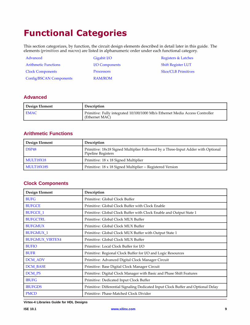
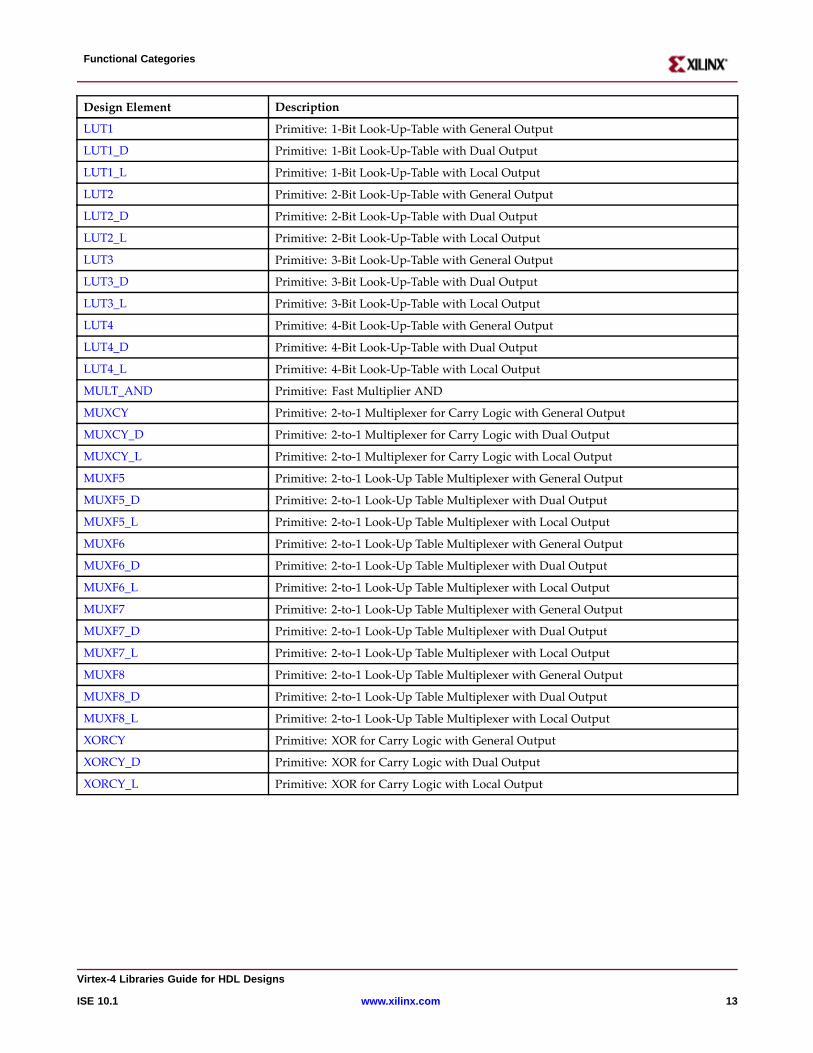
Functional CategoriesThis section categorizes, by function, the circuit design elements described in detail later in this guide. Theelements (primitives and macros) are listed in alphanumeric order under each functional category.
Advanced Gigabit I/O Registers & Latches
Arithmetic Functions I/O Components Shift Register LUT
Clock Components Processors Slice/CLB Primitives
Config/BSCAN Components RAM/ROM
Advanced
Design Element Description
EMAC Primitive: Fully integrated 10/100/1000 Mb/s Ethernet Media Access Controller(Ethernet MAC)
Arithmetic Functions
Design Element Description
DSP48 Primitive: 18x18 Signed Multiplier Followed by a Three-Input Adder with OptionalPipeline Registers
MULT18X18 Primitive: 18 x 18 Signed Multiplier
MULT18X18S Primitive: 18 x 18 Signed Multiplier -- Registered Version
Clock Components
Design Element Description
BUFG Primitive: Global Clock Buffer
BUFGCE Primitive: Global Clock Buffer with Clock Enable
BUFGCE_1 Primitive: Global Clock Buffer with Clock Enable and Output State 1
BUFGCTRL Primitive: Global Clock MUX Buffer
BUFGMUX Primitive: Global Clock MUX Buffer
BUFGMUX_1 Primitive: Global Clock MUX Buffer with Output State 1
BUFGMUX_VIRTEX4 Primitive: Global Clock MUX Buffer
BUFIO Primitive: Local Clock Buffer for I/O
BUFR Primitive: Regional Clock Buffer for I/O and Logic Resources
DCM_ADV Primitive: Advanced Digital Clock Manager Circuit
DCM_BASE Primitive: Base Digital Clock Manager Circuit
DCM_PS Primitive: Digital Clock Manager with Basic and Phase Shift Features
IBUFG Primitive: Dedicated Input Clock Buffer
IBUFGDS Primitive: Differential Signaling Dedicated Input Clock Buffer and Optional Delay
PMCD Primitive: Phase-Matched Clock Divider
Vir tex-4 Libraries Guide for HDL Designs
ISE 10.1 www.xilinx.com 9
Functional Categories
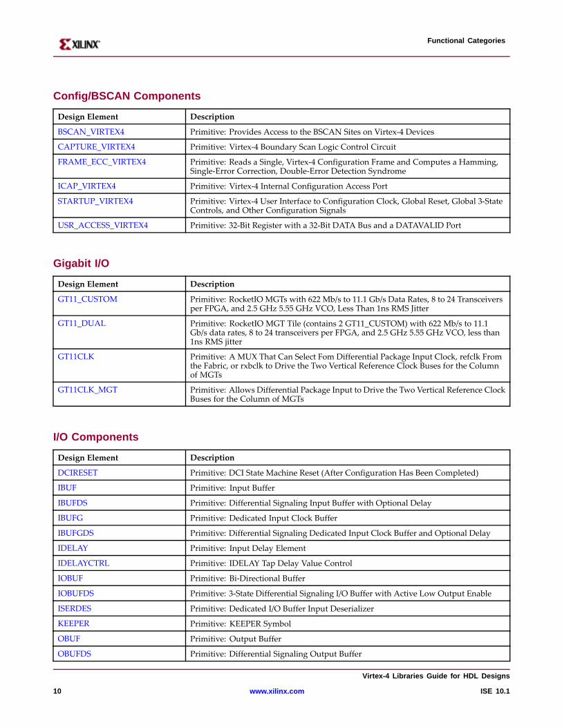
Config/BSCAN Components
Design Element Description
BSCAN_VIRTEX4 Primitive: Provides Access to the BSCAN Sites on Virtex-4 Devices
CAPTURE_VIRTEX4 Primitive: Virtex-4 Boundary Scan Logic Control Circuit
FRAME_ECC_VIRTEX4 Primitive: Reads a Single, Virtex-4 Configuration Frame and Computes a Hamming,Single-Error Correction, Double-Error Detection Syndrome
ICAP_VIRTEX4 Primitive: Virtex-4 Internal Configuration Access Port
STARTUP_VIRTEX4 Primitive: Virtex-4 User Interface to Configuration Clock, Global Reset, Global 3-StateControls, and Other Configuration Signals
USR_ACCESS_VIRTEX4 Primitive: 32-Bit Register with a 32-Bit DATA Bus and a DATAVALID Port
Gigabit I/O
Design Element Description
GT11_CUSTOM Primitive: RocketIO MGTs with 622 Mb/s to 11.1 Gb/s Data Rates, 8 to 24 Transceiversper FPGA, and 2.5 GHz 5.55 GHz VCO, Less Than 1ns RMS Jitter
GT11_DUAL Primitive: RocketIO MGT Tile (contains 2 GT11_CUSTOM) with 622 Mb/s to 11.1Gb/s data rates, 8 to 24 transceivers per FPGA, and 2.5 GHz 5.55 GHz VCO, less than1ns RMS jitter
GT11CLK Primitive: A MUX That Can Select Fom Differential Package Input Clock, refclk Fromthe Fabric, or rxbclk to Drive the Two Vertical Reference Clock Buses for the Columnof MGTs
GT11CLK_MGT Primitive: Allows Differential Package Input to Drive the Two Vertical Reference ClockBuses for the Column of MGTs
I/O Components
Design Element Description
DCIRESET Primitive: DCI State Machine Reset (After Configuration Has Been Completed)
IBUF Primitive: Input Buffer
IBUFDS Primitive: Differential Signaling Input Buffer with Optional Delay
IBUFG Primitive: Dedicated Input Clock Buffer
IBUFGDS Primitive: Differential Signaling Dedicated Input Clock Buffer and Optional Delay
IDELAY Primitive: Input Delay Element
IDELAYCTRL Primitive: IDELAY Tap Delay Value Control
IOBUF Primitive: Bi-Directional Buffer
IOBUFDS Primitive: 3-State Differential Signaling I/O Buffer with Active Low Output Enable
ISERDES Primitive: Dedicated I/O Buffer Input Deserializer
KEEPER Primitive: KEEPER Symbol
OBUF Primitive: Output Buffer
OBUFDS Primitive: Differential Signaling Output Buffer
Vir tex-4 Libraries Guide for HDL Designs
10 www.xilinx.com ISE 10.1
Functional Categories
Design Element Description
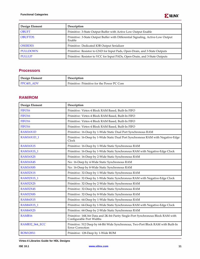
OBUFT Primitive: 3-State Output Buffer with Active Low Output Enable
OBUFTDS Primitive: 3-State Output Buffer with Differential Signaling, Active-Low OutputEnable
OSERDES Primitive: Dedicated IOB Output Serializer
PULLDOWN Primitive: Resistor to GND for Input Pads, Open-Drain, and 3-State Outputs
PULLUP Primitive: Resistor to VCC for Input PADs, Open-Drain, and 3-State Outputs
Processor s
Design Element Description
PPC405_ADV Primitive: Primitive for the Power PC Core
RAM/ROM
Design Element Description
FIFO16 Primitive: Virtex-4 Block RAM Based, Built-In FIFO
FIFO16 Primitive: Virtex-4 Block RAM Based, Built-In FIFO
FIFO16 Primitive: Virtex-4 Block RAM Based, Built-In FIFO
FIFO16 Primitive: Virtex-4 Block RAM Based, Built-In FIFO
RAM16X1D Primitive: 16-Deep by 1-Wide Static Dual Port Synchronous RAM
RAM16X1D_1 Primitive: 16-Deep by 1-Wide Static Dual Port Synchronous RAM with Negative-EdgeClock
RAM16X1S Primitive: 16-Deep by 1-Wide Static Synchronous RAM
RAM16X1S_1 Primitive: 16-Deep by 1-Wide Static Synchronous RAM with Negative-Edge Clock
RAM16X2S Primitive: 16-Deep by 2-Wide Static Synchronous RAM
RAM16X4S No: 16-Deep by 4-Wide Static Synchronous RAM
RAM16X8S No: 16-Deep by 8-Wide Static Synchronous RAM
RAM32X1S Primitive: 32-Deep by 1-Wide Static Synchronous RAM
RAM32X1S_1 Primitive: 32-Deep by 1-Wide Static Synchronous RAM with Negative-Edge Clock
RAM32X2S Primitive: 32-Deep by 2-Wide Static Synchronous RAM
RAM32X4S Primitive: 32-Deep by 4-Wide Static Synchronous RAM
RAM32X8S Primitive: 32-Deep by 8-Wide Static Synchronous RAM
RAM64X1S Primitive: 64-Deep by 1-Wide Static Synchronous RAM
RAM64X1S_1 Primitive: 64-Deep by 1-Wide Static Synchronous RAM with Negative-Edge Clock
RAM64X2S Primitive: 64-Deep by 2-Wide Static Synchronous RAM
RAMB16 Primitive: 16K-bit Data and 2K-bit Parity Single-Port Synchronous Block RAM withConfigurable Port Widths
RAMB32_S64_ECC Primitive: 512 Deep by 64-Bit Wide Synchronous, Two-Port Block RAM with Built-InError Correction
ROM128X1 Primitive: 128-Deep by 1-Wide ROM
Vir tex-4 Libraries Guide for HDL Designs
ISE 10.1 www.xilinx.com 11
Functional Categories
Design Element Description
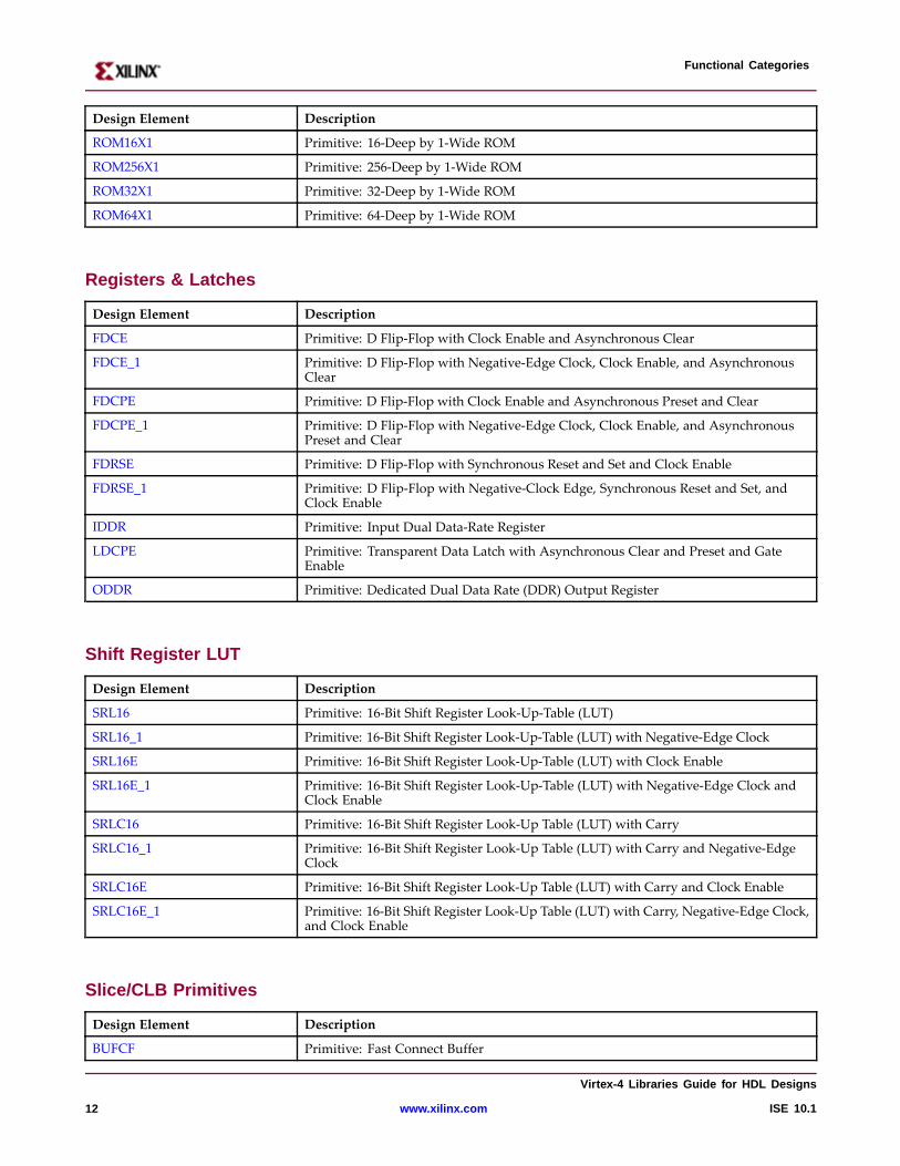
ROM16X1 Primitive: 16-Deep by 1-Wide ROM
ROM256X1 Primitive: 256-Deep by 1-Wide ROM
ROM32X1 Primitive: 32-Deep by 1-Wide ROM
ROM64X1 Primitive: 64-Deep by 1-Wide ROM
Register s & Latc hes
Design Element Description
FDCE Primitive: D Flip-Flop with Clock Enable and Asynchronous Clear
FDCE_1 Primitive: D Flip-Flop with Negative-Edge Clock, Clock Enable, and AsynchronousClear
FDCPE Primitive: D Flip-Flop with Clock Enable and Asynchronous Preset and Clear
FDCPE_1 Primitive: D Flip-Flop with Negative-Edge Clock, Clock Enable, and AsynchronousPreset and Clear
FDRSE Primitive: D Flip-Flop with Synchronous Reset and Set and Clock Enable
FDRSE_1 Primitive: D Flip-Flop with Negative-Clock Edge, Synchronous Reset and Set, andClock Enable
IDDR Primitive: Input Dual Data-Rate Register
LDCPE Primitive: Transparent Data Latch with Asynchronous Clear and Preset and GateEnable
ODDR Primitive: Dedicated Dual Data Rate (DDR) Output Register
Shift Register LUT
Design Element Description
SRL16 Primitive: 16-Bit Shift Register Look-Up-Table (LUT)
SRL16_1 Primitive: 16-Bit Shift Register Look-Up-Table (LUT) with Negative-Edge Clock
SRL16E Primitive: 16-Bit Shift Register Look-Up-Table (LUT) with Clock Enable
SRL16E_1 Primitive: 16-Bit Shift Register Look-Up-Table (LUT) with Negative-Edge Clock andClock Enable
SRLC16 Primitive: 16-Bit Shift Register Look-Up Table (LUT) with Carry
SRLC16_1 Primitive: 16-Bit Shift Register Look-Up Table (LUT) with Carry and Negative-EdgeClock
SRLC16E Primitive: 16-Bit Shift Register Look-Up Table (LUT) with Carry and Clock Enable
SRLC16E_1 Primitive: 16-Bit Shift Register Look-Up Table (LUT) with Carry, Negative-Edge Clock,and Clock Enable
Slice/CLB Primitives
Design Element Description
BUFCF Primitive: Fast Connect Buffer
Vir tex-4 Libraries Guide for HDL Designs
12 www.xilinx.com ISE 10.1
Functional Categories
Design Element Description
LUT1 Primitive: 1-Bit Look-Up-Table with General Output
LUT1_D Primitive: 1-Bit Look-Up-Table with Dual Output
LUT1_L Primitive: 1-Bit Look-Up-Table with Local Output
LUT2 Primitive: 2-Bit Look-Up-Table with General Output
LUT2_D Primitive: 2-Bit Look-Up-Table with Dual Output
LUT2_L Primitive: 2-Bit Look-Up-Table with Local Output
LUT3 Primitive: 3-Bit Look-Up-Table with General Output
LUT3_D Primitive: 3-Bit Look-Up-Table with Dual Output
LUT3_L Primitive: 3-Bit Look-Up-Table with Local Output
LUT4 Primitive: 4-Bit Look-Up-Table with General Output
LUT4_D Primitive: 4-Bit Look-Up-Table with Dual Output
LUT4_L Primitive: 4-Bit Look-Up-Table with Local Output
MULT_AND Primitive: Fast Multiplier AND
MUXCY Primitive: 2-to-1 Multiplexer for Carry Logic with General Output
MUXCY_D Primitive: 2-to-1 Multiplexer for Carry Logic with Dual Output
MUXCY_L Primitive: 2-to-1 Multiplexer for Carry Logic with Local Output
MUXF5 Primitive: 2-to-1 Look-Up Table Multiplexer with General Output
MUXF5_D Primitive: 2-to-1 Look-Up Table Multiplexer with Dual Output
MUXF5_L Primitive: 2-to-1 Look-Up Table Multiplexer with Local Output
MUXF6 Primitive: 2-to-1 Look-Up Table Multiplexer with General Output
MUXF6_D Primitive: 2-to-1 Look-Up Table Multiplexer with Dual Output
MUXF6_L Primitive: 2-to-1 Look-Up Table Multiplexer with Local Output
MUXF7 Primitive: 2-to-1 Look-Up Table Multiplexer with General Output
MUXF7_D Primitive: 2-to-1 Look-Up Table Multiplexer with Dual Output
MUXF7_L Primitive: 2-to-1 Look-Up Table Multiplexer with Local Output
MUXF8 Primitive: 2-to-1 Look-Up Table Multiplexer with General Output
MUXF8_D Primitive: 2-to-1 Look-Up Table Multiplexer with Dual Output
MUXF8_L Primitive: 2-to-1 Look-Up Table Multiplexer with Local Output
XORCY Primitive: XOR for Carry Logic with General Output
XORCY_D Primitive: XOR for Carry Logic with Dual Output
XORCY_L Primitive: XOR for Carry Logic with Local Output
Vir tex-4 Libraries Guide for HDL Designs
ISE 10.1 www.xilinx.com 13

Vir tex-4 Libraries Guide for HDL Designs
14 www.xilinx.com ISE 10.1
About Design Elements
This section describes the design elements that can be used with this architecture. The design elements areorganized alphabetically.
The following information is provided for each design element, where applicable:
• Name of element
• Brief description
• Schematic symbol (if any)
• Logic table (if any)
• Port descriptions
• Usage
• Available attributes (if any)
• Example instantiation code
• For more information
Vir tex-4 Libraries Guide for HDL Designs
ISE 10.1 www.xilinx.com 15
About Design Elements
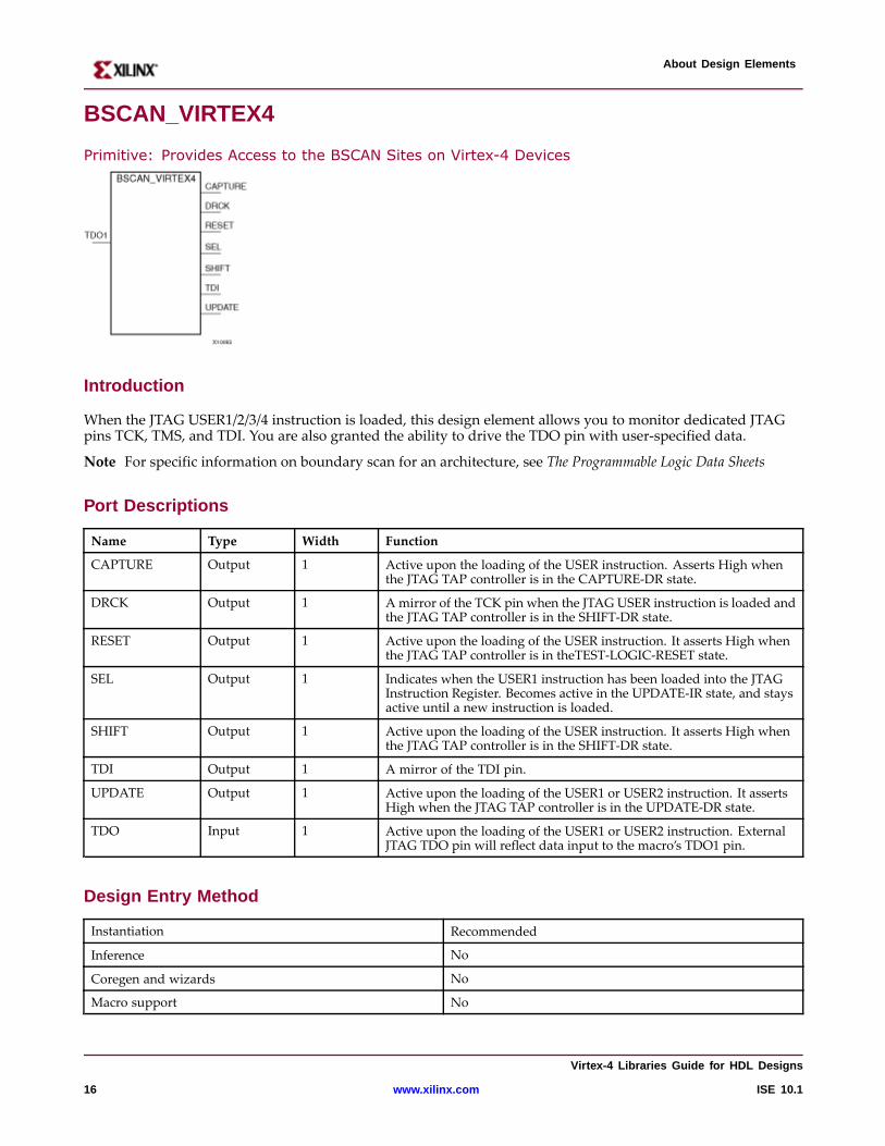
BSCAN_VIRTEX4
Primitive: Provides Access to the BSCAN Sites on Virtex-4 Devices
Intr oduction
When the JTAG USER1/2/3/4 instruction is loaded, this design element allows you to monitor dedicated JTAGpins TCK, TMS, and TDI. You are also granted the ability to drive the TDO pin with user-specified data.
Note For specific information on boundary scan for an architecture, see The Programmable Logic Data Sheets
Por t Descriptions
Name Type Width Function
CAPTURE Output 1 Active upon the loading of the USER instruction. Asserts High whenthe JTAG TAP controller is in the CAPTURE-DR state.
DRCK Output 1 A mirror of the TCK pin when the JTAG USER instruction is loaded andthe JTAG TAP controller is in the SHIFT-DR state.
RESET Output 1 Active upon the loading of the USER instruction. It asserts High whenthe JTAG TAP controller is in theTEST-LOGIC-RESET state.
SEL Output 1 Indicates when the USER1 instruction has been loaded into the JTAGInstruction Register. Becomes active in the UPDATE-IR state, and staysactive until a new instruction is loaded.
SHIFT Output 1 Active upon the loading of the USER instruction. It asserts High whenthe JTAG TAP controller is in the SHIFT-DR state.
TDI Output 1 A mirror of the TDI pin.
UPDATE Output 1 Active upon the loading of the USER1 or USER2 instruction. It assertsHigh when the JTAG TAP controller is in the UPDATE-DR state.
TDO Input 1 Active upon the loading of the USER1 or USER2 instruction. ExternalJTAG TDO pin will reflect data input to the macro’s TDO1 pin.
Design Entr y Method
Instantiation Recommended
Inference No
Coregen and wizards No
Macro support No
Vir tex-4 Libraries Guide for HDL Designs
16 www.xilinx.com ISE 10.1
About Design Elements
Availab le Attrib utes
Attribute Type Allowed Values Default Description
JTAG_CHAIN Integer 1, 2, 3, or 4 1 Used to set the BSCAN site in the device.
VHDL Instantiation Template
Unless they already exist, copy the following two statements and paste them before the entity declaration.Library UNISIM;use UNISIM.vcomponents.all;
-- BSCAN_VIRTEX4: Boundary Scan primitve for connecting internal logic to-- JTAG interface. Virtex-4-- Xilinx HDL Libraries Guide, version 10.1.2
BSCAN_VIRTEX4_inst : BSCAN_VIRTEX4generic map (JTAG_CHAIN => 1) -- Value to set BSCANsite of device. Possible values: (1,2,3 or 4)port map (CAPTURE=> CAPTURE, -- CAPTUREoutput from TAP controllerDRCK=> DRCK, -- Data register output for USER functionsRESET => RESET, -- Reset output from TAP controllerSEL => SEL, -- USER active outputSHIFT => SHIFT, -- SHIFT output from TAP controllerTDI => TDI, -- TDI output from TAP controllerUPDATE=> UPDATE, -- UPDATEoutput from TAP controllerTDO => TDO -- Data input for USER function);
-- End of BSCAN_VIRTEX4_inst instantiation
Verilog Instantiation Template
// BSCAN_VIRTEX4: Boundary Scan primitive for connecting internal logic to// JTAG interface.// Virtex-4// Xilinx HDL Libraries Guide, version 10.1.2
BSCAN_VIRTEX4 #(.JTAG_CHAIN(1) // Possible values: 1, 2, 3, or 4) BSCAN_VIRTEX4_inst (.CAPTURE(CAPTURE), // CAPTUREoutput from TAP controller.DRCK(DRCK), // Data register output for USER function.RESET(RESET), // Reset output from TAP controller.SEL(SEL), // USER active output.SHIFT(SHIFT), // SHIFT output from TAP controller.TDI(TDI), // TDI output from TAP controller.UPDATE(UPDATE), // UPDATEoutput from TAP controller.TDO(TDO) // Data input for USER function);
// End of BSCAN_VIRTEX4_inst instantiation
For More Information
• See the Virtex-4 User Guide.
• See the Virtex-4 Data Sheets.
Vir tex-4 Libraries Guide for HDL Designs
ISE 10.1 www.xilinx.com 17
About Design Elements
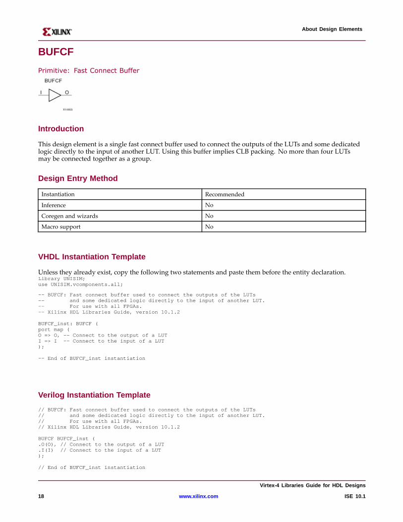
BUFCF
Primitive: Fast Connect Buffer
Intr oduction
This design element is a single fast connect buffer used to connect the outputs of the LUTs and some dedicatedlogic directly to the input of another LUT. Using this buffer implies CLB packing. No more than four LUTsmay be connected together as a group.
Design Entr y Method
Instantiation Recommended
Inference No
Coregen and wizards No
Macro support No
VHDL Instantiation Template
Unless they already exist, copy the following two statements and paste them before the entity declaration.Library UNISIM;use UNISIM.vcomponents.all;
-- BUFCF: Fast connect buffer used to connect the outputs of the LUTs-- and some dedicated logic directly to the input of another LUT.-- For use with all FPGAs.-- Xilinx HDL Libraries Guide, version 10.1.2
BUFCF_inst: BUFCF (port map (O => O, -- Connect to the output of a LUTI => I -- Connect to the input of a LUT);
-- End of BUFCF_inst instantiation
Verilog Instantiation Template
// BUFCF: Fast connect buffer used to connect the outputs of the LUTs// and some dedicated logic directly to the input of another LUT.// For use with all FPGAs.// Xilinx HDL Libraries Guide, version 10.1.2
BUFCF BUFCF_inst (.O(O), // Connect to the output of a LUT.I(I) // Connect to the input of a LUT);
// End of BUFCF_inst instantiation
Vir tex-4 Libraries Guide for HDL Designs
18 www.xilinx.com ISE 10.1

About Design Elements
For More Information
• See the Virtex-4 User Guide.
• See the Virtex-4 Data Sheets.
Vir tex-4 Libraries Guide for HDL Designs
ISE 10.1 www.xilinx.com 19
About Design Elements
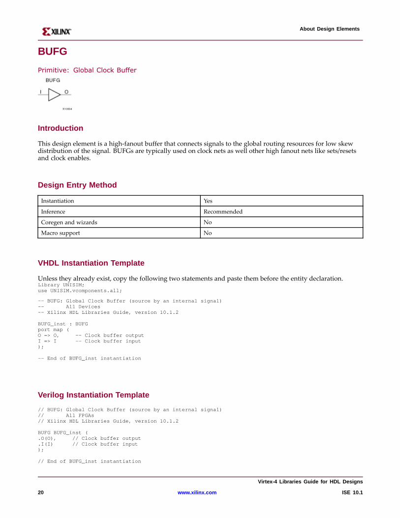
BUFG
Primitive: Global Clock Buffer
Intr oduction
This design element is a high-fanout buffer that connects signals to the global routing resources for low skewdistribution of the signal. BUFGs are typically used on clock nets as well other high fanout nets like sets/resetsand clock enables.
Design Entr y Method
Instantiation Yes
Inference Recommended
Coregen and wizards No
Macro support No
VHDL Instantiation Template
Unless they already exist, copy the following two statements and paste them before the entity declaration.Library UNISIM;use UNISIM.vcomponents.all;
-- BUFG: Global Clock Buffer (source by an internal signal)-- All Devices-- Xilinx HDL Libraries Guide, version 10.1.2
BUFG_inst : BUFGport map (O => O, -- Clock buffer outputI => I -- Clock buffer input);
-- End of BUFG_inst instantiation
Verilog Instantiation Template
// BUFG: Global Clock Buffer (source by an internal signal)// All FPGAs// Xilinx HDL Libraries Guide, version 10.1.2
BUFG BUFG_inst (.O(O), // Clock buffer output.I(I) // Clock buffer input);
// End of BUFG_inst instantiation
Vir tex-4 Libraries Guide for HDL Designs
20 www.xilinx.com ISE 10.1

About Design Elements
For More Information
• See the Virtex-4 User Guide.
• See the Virtex-4 Data Sheets.
Vir tex-4 Libraries Guide for HDL Designs
ISE 10.1 www.xilinx.com 21
About Design Elements
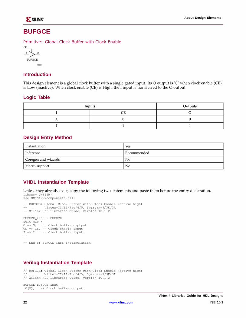
BUFGCE
Primitive: Global Clock Buffer with Clock Enable
Intr oduction
This design element is a global clock buffer with a single gated input. Its O output is "0" when clock enable (CE)is Low (inactive). When clock enable (CE) is High, the I input is transferred to the O output.
Logic Table
Inputs Outputs
I CE O
X 0 0
I 1 I
Design Entr y Method
Instantiation Yes
Inference Recommended
Coregen and wizards No
Macro support No
VHDL Instantiation Template
Unless they already exist, copy the following two statements and paste them before the entity declaration.Library UNISIM;use UNISIM.vcomponents.all;
-- BUFGCE: Global Clock Buffer with Clock Enable (active high)-- Virtex-II/II-Pro/4/5, Spartan-3/3E/3A-- Xilinx HDL Libraries Guide, version 10.1.2
BUFGCE_inst : BUFGCEport map (O => O, -- Clock buffer ouptputCE => CE, -- Clock enable inputI => I -- Clock buffer input);
-- End of BUFGCE_inst instantiation
Verilog Instantiation Template
// BUFGCE: Global Clock Buffer with Clock Enable (active high)// Virtex-II/II-Pro/4/5, Spartan-3/3E/3A// Xilinx HDL Libraries Guide, version 10.1.2
BUFGCEBUFGCE_inst (.O(O), // Clock buffer output
Vir tex-4 Libraries Guide for HDL Designs
22 www.xilinx.com ISE 10.1

About Design Elements
.CE(CE), // Clock enable input
.I(I) // Clock buffer input);
// End of BUFGCE_inst instantiation
For More Information
• See the Virtex-4 User Guide.
• See the Virtex-4 Data Sheets.
Vir tex-4 Libraries Guide for HDL Designs
ISE 10.1 www.xilinx.com 23
About Design Elements
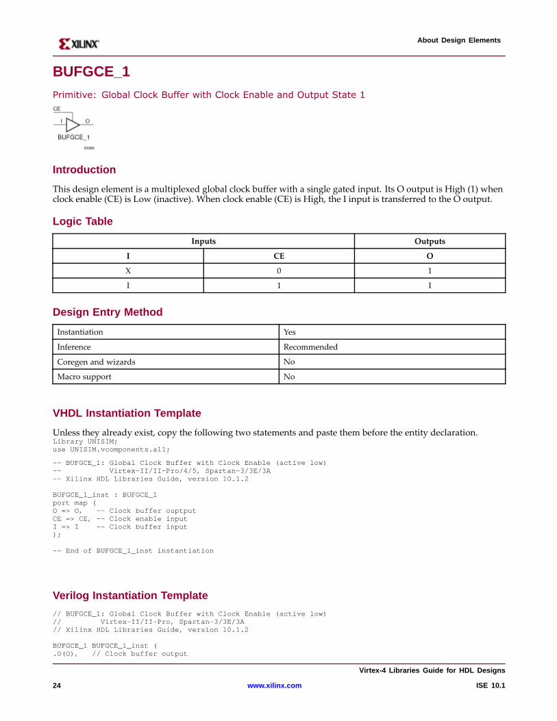
BUFGCE_1
Primitive: Global Clock Buffer with Clock Enable and Output State 1
Intr oduction
This design element is a multiplexed global clock buffer with a single gated input. Its O output is High (1) whenclock enable (CE) is Low (inactive). When clock enable (CE) is High, the I input is transferred to the O output.
Logic Table
Inputs Outputs
I CE O
X 0 1
I 1 I
Design Entr y Method
Instantiation Yes
Inference Recommended
Coregen and wizards No
Macro support No
VHDL Instantiation Template
Unless they already exist, copy the following two statements and paste them before the entity declaration.Library UNISIM;use UNISIM.vcomponents.all;
-- BUFGCE_1: Global Clock Buffer with Clock Enable (active low)-- Virtex-II/II-Pro/4/5, Spartan-3/3E/3A-- Xilinx HDL Libraries Guide, version 10.1.2
BUFGCE_1_inst : BUFGCE_1port map (O => O, -- Clock buffer ouptputCE => CE, -- Clock enable inputI => I -- Clock buffer input);
-- End of BUFGCE_1_inst instantiation
Verilog Instantiation Template
// BUFGCE_1: Global Clock Buffer with Clock Enable (active low)// Virtex-II/II-Pro, Spartan-3/3E/3A// Xilinx HDL Libraries Guide, version 10.1.2
BUFGCE_1BUFGCE_1_inst (.O(O), // Clock buffer output
Vir tex-4 Libraries Guide for HDL Designs
24 www.xilinx.com ISE 10.1

About Design Elements
.CE(CE), // Clock enable input
.I(I) // Clock buffer input);
// End of BUFGCE_1_inst instantiation
For More Information
• See the Virtex-4 User Guide.
• See the Virtex-4 Data Sheets.
Vir tex-4 Libraries Guide for HDL Designs
ISE 10.1 www.xilinx.com 25
About Design Elements
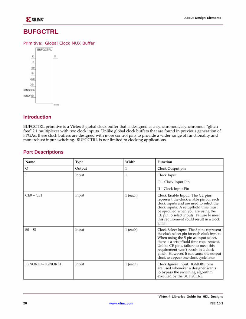
BUFGCTRL
Primitive: Global Clock MUX Buffer
Intr oduction
BUFGCTRL primitive is a Virtex-5 global clock buffer that is designed as a synchronous/asynchronous "glitchfree" 2:1 multiplexer with two clock inputs. Unlike global clock buffers that are found in previous generation ofFPGAs, these clock buffers are designed with more control pins to provide a wider range of functionality andmore robust input switching. BUFGCTRL is not limited to clocking applications.
Por t Descriptions
Name Type Width Function
O Output 1 Clock Output pin
I Input 1 Clock Input:
I0 – Clock Input Pin
I1 - Clock Input Pin
CE0 – CE1 Input 1 (each) Clock Enable Input. The CE pinsrepresent the clock enable pin for eachclock inputs and are used to select theclock inputs. A setup/hold time mustbe specified when you are using theCE pin to select inputs. Failure to meetthis requirement could result in a clockglitch.
S0 – S1 Input 1 (each) Clock Select Input. The S pins representthe clock select pin for each clock inputs.When using the S pin as input select,there is a setup/hold time requirement.Unlike CE pins, failure to meet thisrequirement won’t result in a clockglitch. However, it can cause the outputclock to appear one clock cycle later.
IGNORE0 – IGNORE1 Input 1 (each) Clock Ignore Input. IGNORE pinsare used whenever a designer wantsto bypass the switching algorithmexecuted by the BUFGCTRL.
Vir tex-4 Libraries Guide for HDL Designs
26 www.xilinx.com ISE 10.1
About Design Elements
Design Entr y Method
Instantiation Yes
Inference Recommended
Coregen and wizards No
Macro support No
Availab le Attrib utes
Attribute Type Allowed Values Default Description
INIT_OUT Integer 0 or 1 0 Initializes the BUFGCTRLoutput to the specified valueafter configuration.
PRESELECT_I0 Boolean FALSE, TRUE FALSE If TRUE, BUFGCTRLoutput uses I0 input afterconfiguration.
PRESELECT_I1 Boolean FALSE, TRUE FALSE If TRUE, BUFGCTRLoutput uses I1 input afterconfiguration.
Note Both PRESELECT attributes might not be TRUE at the same time.
For More Information
• See the Virtex-4 User Guide.
• See the Virtex-4 Data Sheets.
Vir tex-4 Libraries Guide for HDL Designs
ISE 10.1 www.xilinx.com 27
About Design Elements
BUFGMUX
Primitive: Global Clock MUX Buffer
Intr oduction
BUFGMUX is a multiplexed global clock buffer, based off of the BUFGCTRL, that can select between two inputclocks: I0 and I1. When the select input (S) is Low, the signal on I0 is selected for output (O). When the selectinput (S) is High, the signal on I1 is selected for output.
BUFGMUX and BUFGMUX_1 are distinguished by the state the output assumes when that output switchesbetween clocks in response to a change in its select input. BUGFMUX assumes output state 0 and BUFGMUX_1assumes output state 1.
Note BUFGMUX guarantees that when S is toggled, the state of the output remains in the inactive state untilthe next active clock edge (either I0 or I1) occurs.
Logic Table
Inputs Outputs
I0 I1 S O
I0 X 0 I0
X I1 1 I1
X X ↑ 0
X X ↓ 0
Design Entr y Method
Instantiation Yes
Inference Recommended
Coregen and wizards No
Macro support No
VHDL Instantiation Template
Unless they already exist, copy the following two statements and paste them before the entity declaration.Library UNISIM;use UNISIM.vcomponents.all;
-- BUFGMUX:Global Clock Buffer 2-to-1 MUX-- Virtex-II/II-Pro/4/5, Spartan-3/3E/3A-- Xilinx HDL Libraries Guide, version 10.1.2
BUFGMUX_inst : BUFGMUXport map (O => O, -- Clock MUXoutputI0 => I0, -- Clock0 inputI1 => I1, -- Clock1 inputS => S -- Clock select input);
Vir tex-4 Libraries Guide for HDL Designs
28 www.xilinx.com ISE 10.1
About Design Elements
-- End of BUFGMUX_inst instantiation
Verilog Instantiation Template
// BUFGMUX:Global Clock Buffer 2-to-1 MUX// Virtex-II/II-Pro/4/5, Spartan-3/3E/3A// Xilinx HDL Libraries Guide, version 10.1.2
BUFGMUXBUFGMUX_inst (.O(O), // Clock MUXoutput.I0(I0), // Clock0 input.I1(I1), // Clock1 input.S(S) // Clock select input);
// End of BUFGMUX_inst instantiation
For More Information
• See the Virtex-4 User Guide.
• See the Virtex-4 Data Sheets.
Vir tex-4 Libraries Guide for HDL Designs
ISE 10.1 www.xilinx.com 29
About Design Elements
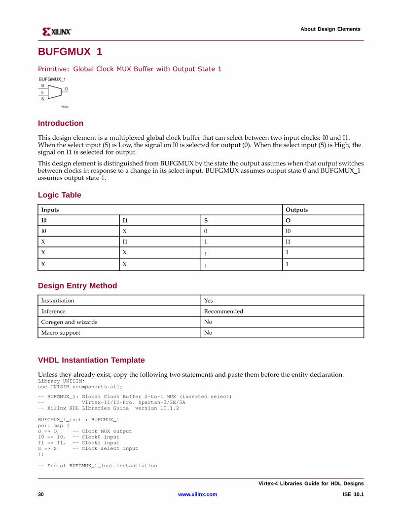
BUFGMUX_1
Primitive: Global Clock MUX Buffer with Output State 1
Intr oduction
This design element is a multiplexed global clock buffer that can select between two input clocks: I0 and I1.When the select input (S) is Low, the signal on I0 is selected for output (0). When the select input (S) is High, thesignal on I1 is selected for output.
This design element is distinguished from BUFGMUX by the state the output assumes when that output switchesbetween clocks in response to a change in its select input. BUFGMUX assumes output state 0 and BUFGMUX_1assumes output state 1.
Logic Table
Inputs Outputs
I0 I1 S O
I0 X 0 I0
X I1 1 I1
X X ↑ 1
X X ↓ 1
Design Entr y Method
Instantiation Yes
Inference Recommended
Coregen and wizards No
Macro support No
VHDL Instantiation Template
Unless they already exist, copy the following two statements and paste them before the entity declaration.Library UNISIM;use UNISIM.vcomponents.all;
-- BUFGMUX_1: Global Clock Buffer 2-to-1 MUX (inverted select)-- Virtex-II/II-Pro, Spartan-3/3E/3A-- Xilinx HDL Libraries Guide, version 10.1.2
BUFGMUX_1_inst : BUFGMUX_1port map (O => O, -- Clock MUXoutputI0 => I0, -- Clock0 inputI1 => I1, -- Clock1 inputS => S -- Clock select input);
-- End of BUFGMUX_1_inst instantiation
Vir tex-4 Libraries Guide for HDL Designs
30 www.xilinx.com ISE 10.1
About Design Elements
Verilog Instantiation Template
// BUFGMUX_1: Global Clock Buffer 2-to-1 MUX (inverted select)// Virtex-II/II-Pro, Spartan-3/3E/3A// Xilinx HDL Libraries Guide, version 10.1.2
BUFGMUX_1BUFGMUX_1_inst (.O(O), // Clock MUXoutput.I0(I0), // Clock0 input.I1(I1), // Clock1 input.S(S) // Clock select input);
// End of BUFGMUX_1_inst instantiation
For More Information
• See the Virtex-4 User Guide.
• See the Virtex-4 Data Sheets.
Vir tex-4 Libraries Guide for HDL Designs
ISE 10.1 www.xilinx.com 31
About Design Elements
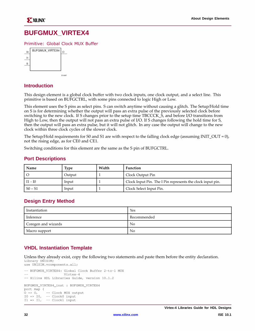
BUFGMUX_VIRTEX4
Primitive: Global Clock MUX Buffer
Intr oduction
This design element is a global clock buffer with two clock inputs, one clock output, and a select line. Thisprimitive is based on BUFGCTRL, with some pins connected to logic High or Low.
This element uses the S pins as select pins. S can switch anytime without causing a glitch. The Setup/Hold timeon S is for determining whether the output will pass an extra pulse of the previously selected clock beforeswitching to the new clock. If S changes prior to the setup time TBCCCK_S, and before I/O transitions fromHigh to Low, then the output will not pass an extra pulse of I/O. If S changes following the hold time for S,then the output will pass an extra pulse, but it will not glitch. In any case the output will change to the newclock within three clock cycles of the slower clock.
The Setup/Hold requirements for S0 and S1 are with respect to the falling clock edge (assuming INIT_OUT = 0),not the rising edge, as for CE0 and CE1.
Switching conditions for this element are the same as the S pin of BUFGCTRL.
Por t Descriptions
Name Type Width Function
O Output 1 Clock Output Pin
I1 - I0 Input 1 Clock Input Pin. The I Pin represents the clock input pin.
S0 – S1 Input 1 Clock Select Input Pin.
Design Entr y Method
Instantiation Yes
Inference Recommended
Coregen and wizards No
Macro support No
VHDL Instantiation Template
Unless they already exist, copy the following two statements and paste them before the entity declaration.Library UNISIM;use UNISIM.vcomponents.all;
-- BUFGMUX_VIRTEX4: Global Clock Buffer 2-to-1 MUX-- Virtex-4-- Xilinx HDL Libraries Guide, version 10.1.2
BUFGMUX_VIRTEX4_inst : BUFGMUX_VIRTEX4port map (O => O, -- Clock MUXoutputI0 => I0, -- Clock0 inputI1 => I1, -- Clock1 input
Vir tex-4 Libraries Guide for HDL Designs
32 www.xilinx.com ISE 10.1
About Design Elements
S => S -- Clock select input);
-- End of BUFGMUX_VIRTEX4_inst instantiation
Verilog Instantiation Template
// BUFGMUX_VIRTEX4: Global Clock Buffer 2-to-1 MUX// Virtex-4// Xilinx HDL Libraries Guide, version 10.1.2
BUFGMUX_VIRTEX4BUFGMUX_VIRTEX4_inst (.O(O), // Clock MUXoutput.I0(I0), // Clock0 input.I1(I1), // Clock1 input.S(S) // Clock select input);
// End of BUFGMUX_VIRTEX4_inst instantiation
For More Information
• See the Virtex-4 User Guide.
• See the Virtex-4 Data Sheets.
Vir tex-4 Libraries Guide for HDL Designs
ISE 10.1 www.xilinx.com 33
About Design Elements
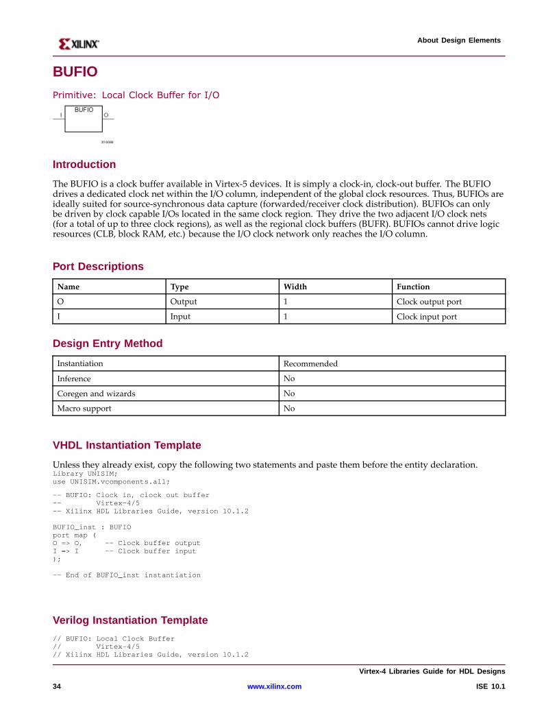
BUFIO
Primitive: Local Clock Buffer for I/O
Intr oduction
The BUFIO is a clock buffer available in Virtex-5 devices. It is simply a clock-in, clock-out buffer. The BUFIOdrives a dedicated clock net within the I/O column, independent of the global clock resources. Thus, BUFIOs areideally suited for source-synchronous data capture (forwarded/receiver clock distribution). BUFIOs can onlybe driven by clock capable I/Os located in the same clock region. They drive the two adjacent I/O clock nets(for a total of up to three clock regions), as well as the regional clock buffers (BUFR). BUFIOs cannot drive logicresources (CLB, block RAM, etc.) because the I/O clock network only reaches the I/O column.
Por t Descriptions
Name Type Width Function
O Output 1 Clock output port
I Input 1 Clock input port
Design Entr y Method
Instantiation Recommended
Inference No
Coregen and wizards No
Macro support No
VHDL Instantiation Template
Unless they already exist, copy the following two statements and paste them before the entity declaration.Library UNISIM;use UNISIM.vcomponents.all;
-- BUFIO: Clock in, clock out buffer-- Virtex-4/5-- Xilinx HDL Libraries Guide, version 10.1.2
BUFIO_inst : BUFIOport map (O => O, -- Clock buffer outputI => I -- Clock buffer input);
-- End of BUFIO_inst instantiation
Verilog Instantiation Template
// BUFIO: Local Clock Buffer// Virtex-4/5// Xilinx HDL Libraries Guide, version 10.1.2
Vir tex-4 Libraries Guide for HDL Designs
34 www.xilinx.com ISE 10.1
About Design Elements
BUFIO BUFIO_inst (.O(O), // Clock buffer output.I(I) // Clock buffer input);
// End of BUFIO_inst instantiation
For More Information
• See the Virtex-4 User Guide.
• See the Virtex-4 Data Sheets.
Vir tex-4 Libraries Guide for HDL Designs
ISE 10.1 www.xilinx.com 35
About Design Elements
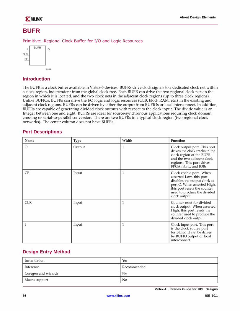
BUFR
Primitive: Regional Clock Buffer for I/O and Logic Resources
Intr oduction
The BUFR is a clock buffer available in Virtex-5 devices. BUFRs drive clock signals to a dedicated clock net withina clock region, independent from the global clock tree. Each BUFR can drive the two regional clock nets in theregion in which it is located, and the two clock nets in the adjacent clock regions (up to three clock regions).Unlike BUFIOs, BUFRs can drive the I/O logic and logic resources (CLB, block RAM, etc.) in the existing andadjacent clock regions. BUFRs can be driven by either the output from BUFIOs or local interconnect. In addition,BUFRs are capable of generating divided clock outputs with respect to the clock input. The divide value is anInteger between one and eight. BUFRs are ideal for source-synchronous applications requiring clock domaincrossing or serial-to-parallel conversion. There are two BUFRs in a typical clock region (two regional clocknetworks). The center column does not have BUFRs.
Por t Descriptions
Name Type Width Function
O Output 1 Clock output port. This portdrives the clock tracks in theclock region of the BUFRand the two adjacent clockregions. This port drivesFPGA fabric, and IOBs.
CE Input 1 Clock enable port. Whenasserted Low, this portdisables the output clock atport O. When asserted High,this port resets the counterused to produce the dividedclock output.
CLR Input 1 Counter reset for dividedclock output. When assertedHigh, this port resets thecounter used to produce thedivided clock output.
I Input 1 Clock input port. This portis the clock source portfor BUFR. It can be drivenby BUFIO output or localinterconnect.
Design Entr y Method
Instantiation Yes
Inference Recommended
Coregen and wizards No
Macro support No
Vir tex-4 Libraries Guide for HDL Designs
36 www.xilinx.com ISE 10.1
About Design Elements
Availab le Attrib utes
Attribute Type Allowed Values Default Description
BUFR_DIVIDE String "BYPASS", "1", "2", "3","4", "5", "6", "7", "8
"BYPASS” Defines whether the outputclock is a divided version ofinput clock.
SIM_DEVICE String “VIRTEX4”, “VIRTEX5” “VIRTEX4” Device selection.
VHDL Instantiation Template
Unless they already exist, copy the following two statements and paste them before the entity declaration.Library UNISIM;use UNISIM.vcomponents.all;
-- BUFR: Regional (Local) Clock Buffer /w Enable, Clear and Division Capabilities-- Virtex-4/5-- Xilinx HDL Libraries Guide, version 10.1.2
BUFR_inst : BUFRgeneric map (BUFR_DIVIDE => "BYPASS", -- "BYPASS", "1", "2", "3", "4", "5", "6", "7", "8"SIM_DEVICE => "VIRTEX4") -- Specify target device, "VIRTEX4" or "VIRTEX5"port map (O => O, -- Clock buffer outputCE => CE, -- Clock enable inputCLR => CLR, -- Clock buffer reset inputI => I -- Clock buffer input);
-- End of BUFR_inst instantiation
Verilog Instantiation Template
// BUFR: Regional Clock Buffer /w Enable, Clear and Division Capabilities// Virtex-4/5// Xilinx HDL Libraries Guide, version 10.1.2
BUFR #(.BUFR_DIVIDE("BYPASS"), // "BYPASS", "1", "2", "3", "4", "5", "6", "7", "8".SIM_DEVICE("VIRTEX4") // Specify target device, "VIRTEX4" or "VIRTEX5") BUFR_inst (.O(O), // Clock buffer output.CE(CE), // Clock enable input.CLR(CLR), // Clock buffer reset input.I(I) // Clock buffer input);
// End of BUFR_inst instantiation
For More Information
• See the Virtex-4 User Guide.
• See the Virtex-4 Data Sheets.
Vir tex-4 Libraries Guide for HDL Designs
ISE 10.1 www.xilinx.com 37
About Design Elements
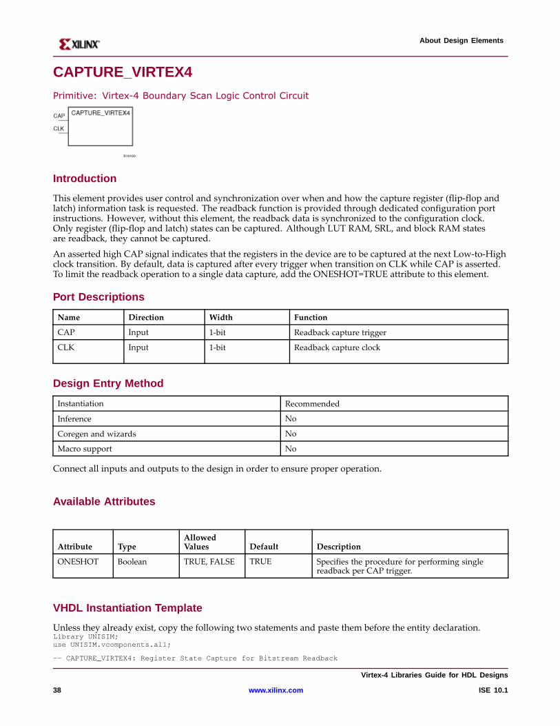
CAPTURE_VIRTEX4
Primitive: Virtex-4 Boundary Scan Logic Control Circuit
Intr oduction
This element provides user control and synchronization over when and how the capture register (flip-flop andlatch) information task is requested. The readback function is provided through dedicated configuration portinstructions. However, without this element, the readback data is synchronized to the configuration clock.Only register (flip-flop and latch) states can be captured. Although LUT RAM, SRL, and block RAM statesare readback, they cannot be captured.
An asserted high CAP signal indicates that the registers in the device are to be captured at the next Low-to-Highclock transition. By default, data is captured after every trigger when transition on CLK while CAP is asserted.To limit the readback operation to a single data capture, add the ONESHOT=TRUE attribute to this element.
Por t Descriptions
Name Direction Width Function
CAP Input 1-bit Readback capture trigger
CLK Input 1-bit Readback capture clock
Design Entr y Method
Instantiation Recommended
Inference No
Coregen and wizards No
Macro support No
Connect all inputs and outputs to the design in order to ensure proper operation.
Availab le Attrib utes
Attribute TypeAllowedValues Default Description
ONESHOT Boolean TRUE, FALSE TRUE Specifies the procedure for performing singlereadback per CAP trigger.
VHDL Instantiation Template
Unless they already exist, copy the following two statements and paste them before the entity declaration.Library UNISIM;use UNISIM.vcomponents.all;
-- CAPTURE_VIRTEX4: Register State Capture for Bitstream Readback
Vir tex-4 Libraries Guide for HDL Designs
38 www.xilinx.com ISE 10.1
About Design Elements
-- Virtex-4-- Xilinx HDL Libraries Guide, version 10.1.2
CAPTURE_VIRTEX4_inst : CAPTURE_VIRTEX4generic map (ONESHOT=> TRUE) -- TRUE or FALSEport map (CAP => CAP, -- Capture inputCLK => CLK -- Clock input);-- End of CAPTURE_VIRTEX4_inst instantiation
Verilog Instantiation Template
// CAPTURE_VIRTEX4: Register State Capture for Bitstream Readback// Virtex-4// Xilinx HDL Libraries Guide, version 10.1.2
CAPTURE_VIRTEX4#(.ONESHOT("TRUE") // "TRUE" or "FALSE") CAPTURE_VIRTEX4_inst (.CAP(CAP), // Capture input.CLK(CLK) // Clock input);
// End of CAPTURE_VIRTEX4_inst instantiation
For More Information
• See the Virtex-4 User Guide.
• See the Virtex-4 Data Sheets.
Vir tex-4 Libraries Guide for HDL Designs
ISE 10.1 www.xilinx.com 39
About Design Elements
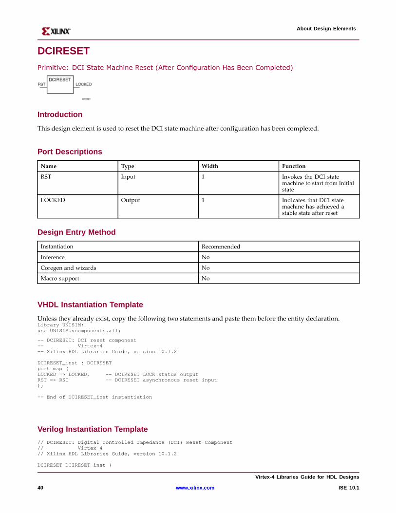
DCIRESET
Primitive: DCI State Machine Reset (After Configuration Has Been Completed)
Intr oduction
This design element is used to reset the DCI state machine after configuration has been completed.
Por t Descriptions
Name Type Width Function
RST Input 1 Invokes the DCI statemachine to start from initialstate
LOCKED Output 1 Indicates that DCI statemachine has achieved astable state after reset
Design Entr y Method
Instantiation Recommended
Inference No
Coregen and wizards No
Macro support No
VHDL Instantiation Template
Unless they already exist, copy the following two statements and paste them before the entity declaration.Library UNISIM;use UNISIM.vcomponents.all;
-- DCIRESET: DCI reset component-- Virtex-4-- Xilinx HDL Libraries Guide, version 10.1.2
DCIRESET_inst : DCIRESETport map (LOCKED=> LOCKED, -- DCIRESET LOCK status outputRST => RST -- DCIRESET asynchronous reset input);
-- End of DCIRESET_inst instantiation
Verilog Instantiation Template
// DCIRESET: Digital Controlled Impedance (DCI) Reset Component// Virtex-4// Xilinx HDL Libraries Guide, version 10.1.2
DCIRESET DCIRESET_inst (
Vir tex-4 Libraries Guide for HDL Designs
40 www.xilinx.com ISE 10.1
About Design Elements
.LOCKED(LOCKED), // 1-bit DCI LOCKEDOutput
.RST(RST) // 1-bit DCI Reset Input);
// End of DCIRESET_inst instantiation
For More Information
• See the Virtex-4 User Guide.
• See the Virtex-4 Data Sheets.
Vir tex-4 Libraries Guide for HDL Designs
ISE 10.1 www.xilinx.com 41
About Design Elements
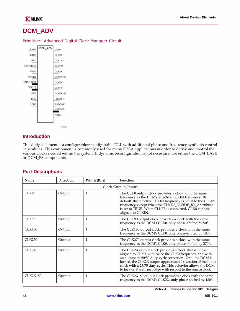
DCM_ADV
Primitive: Advanced Digital Clock Manager Circuit
Intr oduction
This design element is a configurable/reconfigurable DLL with additional phase and frequency synthesis controlcapabilities. This component is commonly used for many FPGA applications in order to derive and control thevarious clocks needed within the system. If dynamic reconfiguration is not necessary, use either the DCM_BASEor DCM_PS components.
Por t Descriptions
Name Direction Width (Bits) Function
Clock Outputs/Inputs
CLK0 Output 1 The CLK0 output clock provides a clock with the samefrequency as the DCM’s effective CLKIN frequency. Bydefault, the effective CLKIN frequency is equal to the CLKINfrequency, except when the CLKIN_DIVIDE_BY_2 attributeis set to TRUE. When CLKFB is connected, CLK0 is phasealigned to CLKIN.
CLK90 Output 1 The CLK90 output clock provides a clock with the samefrequency as the DCM’s CLK0, only phase-shifted by 90°.
CLK180 Output 1 The CLK180 output clock provides a clock with the samefrequency as the DCM’s CLK0, only phase-shifted by 180°.
CLK270 Output 1 The CLK270 output clock provides a clock with the samefrequency as the DCM’s CLK0, only phase-shifted by 270°.
CLK2X Output 1 The CLK2X output clock provides a clock that is phasealigned to CLK0, with twice the CLK0 frequency, and withan automatic 50/50 duty-cycle correction. Until the DCM islocked, the CLK2X output appears as a 1x version of the inputclock with a 25/75 duty cycle. This behavior allows the DCMto lock on the correct edge with respect to the source clock.
CLK2X180 Output 1 The CLK2X180 output clock provides a clock with the samefrequency as the DCM’s CLK2X, only phase-shifted by 180°.
Vir tex-4 Libraries Guide for HDL Designs
42 www.xilinx.com ISE 10.1
About Design Elements
Name Direction Width (Bits) Function
CLKDV Output 1 The frequency divide (CLKDV) output clock provides aclock that is phase aligned to CLK0 with a frequency that isa fraction of the effective CLKIN frequency. The fraction isdetermined by the CLKDV_DIVIDE attribute. By default, theeffective CLKIN frequency is equal to the CLKIN frequency,except when the CLKIN_DIVIDE_BY_2 attribute is set toTRUE.
CLKFX Output 1 The frequency (CLKFX) output clock provides a clock withthe following frequency definition:
CLKFX Frequency = (M/D) x (Effective CLKIN Frequency).
In this equation, M is the multiplier (numerator), with avalue defined by the CLKFX_MULTIPLY attribute. D isthe divisor (denominator), with a value defined by theCLKFX_DIVIDE attribute. Specifications for M and D, aswell as input and output frequency ranges for the frequencysynthesizer, are provided in the Virtex-5 Data Sheet. Therising edge of CLKFX output is phase aligned to the risingedges of CLK0, CLK2X, and CLKDV when the feedback path(CLKFB) is used. When M and D do have no common factor,the alignment occurs only once every D cycles of CLK0. Bydefault, the effective CLKIN frequency is equal to the CLKINfrequency, except when the CLKIN_DIVIDE_BY_2 attributeis set to TRUE.
CLKFX180 Output 1 The CLKFX180 output clock provides a clock with the samefrequency as the DCM’s CLKFX only phase-shifted by 180°.
CLKIN Input 1 The source clock (CLKIN) input pin provides the source clockto the DCM. The CLKIN frequency must fall in the rangesspecified in the Virtex-5 Data Sheet. The clock input signalcomes from one of the following buffers:
1. IBUFG - Global Clock Input Buffer. The DCM compensatesfor the clock input path when an IBUFG, on the same edge(top or bottom) of the device, such as the DCM, is used.
2. BUFG/BUFGCTRL - Internal Global Clock Buffer. AnyBUFGCTRL can drive any DCM in the Virtex-5 device usingthe dedicated global routing. A BUFGCTRL can drive theDCM CLKIN pin when used to connect two DCM in series.
3. IBUF - Input Buffer. When IBUF drives CLKIN input,the PAD to DCM input skew is not compensated andincreased jitter can occur. This configuration is generally notrecommended.
CLKFB Input 1 The feedback clock (CLKFB) input pin provides a referenceor feedback signal to the DCM to delay-compensate theclock outputs and align it with the clock input. To providethe necessary feedback to the DCM, connect only the CLK0output to the CLKFB input via a BUFG component in thecase of internal feedback or an OBUF ’ IBUFG to the caseof external feedback. Set the CLK_FEEDBACK attribute to1X. When the CLKFB pin is connected, CLK0, CLKDV, andCLKFX are phase aligned to CLKIN. When the CLKFB pin isnot connected, set CLK_FEEDBACK to NONE and only theCLKFX and CLKFX180 outputs are valid, however, not phasealigned to CLKIN.
Status Outputs / Control Inputs
Vir tex-4 Libraries Guide for HDL Designs
ISE 10.1 www.xilinx.com 43
About Design Elements
Name Direction Width (Bits) Function
LOCKED Output 1 Synchronous output from the PLL that provides you with anindication that the PLL has achieved phase alignment andis ready for operation.
PSDONE Output 1 Dynamic CLKIN select input. When high, ’1’ CLKIN1 isselected and while low, ’0’ CLKIN2 is selected. If dual clockselection is not necessary, connect this input to a logic 1.
RST Input 1 The reset (RST) input pin resets the DCM circuitry. TheRST signal is an active High asynchronous reset. Assertingthe RST signal asynchronously forces all DCM outputsLow (the LOCKED signal, all status signals, and all outputclocks within four source clock cycles). Because the resetis asynchronous, the last cycle of the clocks can exhibit anunintended short pulse, severely distorted duty-cycle, andno longer phase adjust with respect to one another whiledeasserting. The RST pin must be used when reconfiguringthe device or changing the input frequency. Deassertingthe RST signal synchronously starts the locking process atthe next CLKIN cycle. To ensure a proper DCM reset andlocking process, the RST signal must be deasserted after theCLKIN signal has been present and stable for at least threeclock cycles. In all designs, the DCM must be held in resetuntil the clock is stable. During configuration, the DCM isautomatically held in reset until GSR is released. If the clockis stable when GSR is released.
PSCLK Input 1 The phase-shift clock (PSCLK) input pin provides the sourceclock for the DCM phase shift. The phase-shift clock signalcan be driven by any clock source (external or internal),including:
The frequency range of PSCLK is defined byPSCLK_FREQ_LF/HF (see the Virtex-5 Data Sheet). This inputmust be tied to ground when the CLKOUT_PHASE_SHIFTattribute is set to NONE or FIXED.
PSINCDEC Input 1 The PSINCDEC input signal is synchronous with PSCLK. ThePSINCDEC input signal is used to increment or decrementthe phase-shift factor when CLKOUT_PHASE_SHIFT is setto one of the variable modes. As a result, the output clockis phase shifted. the PSINCDEC signal is asserted High forincrement, or deasserted Low for decrement. This inputmust be tied to ground when the CLKOUT_PHASE_SHIFTattribute is set to NONE or FIXED.
PSEN Input 1 The PSEN input signal is synchronous with PSCLK. Avariable phase-shift operation is initiated by the PSEN inputsignal when CLKOUT_PHASE_SHIFT is set to a variablemode. It must be activated for one period of PSCLK. AfterPSEN is initiated, the phase change is effective for up to 100CLKIN pulse cycles, plus three PSCLK cycles, and is indicatedby a High pulse on PSDONE. There are no sporadic changesor glitches on any output during the phase transition. Fromthe time PSEN is enabled until PSDONE is flagged, the DCMoutput clock moves bit-by-bit from its original phase shiftto the target phase shift. The phase-shift is complete whenPSDONE is flagged. PSEN must be tied to ground when theCLKOUT_PHASE_SHIFT attribute is set to NONE or FIXED.
Dynamic Reconfiguration / DCM Status
For more information on Dynamic Configuration, please see the Configuration User Guide.
Vir tex-4 Libraries Guide for HDL Designs
44 www.xilinx.com ISE 10.1
About Design Elements
Name Direction Width (Bits) Function
DO Output 16 The DO output bus provides DCM status when not using thedynamic reconfiguration feature, and a data output whenusing the dynamic reconfiguration. When showing DCMstatus, the following mapping applies:
DO[0] - Phase-shift overflow
DO[1] CLKIN stopped
DO[2] - CLKFX stopped
DO[3] - CLKFB stopped
DO[15:4] - Not assigned
DRDY Output 1 The DRDY output pin provides ready status for the DCM’sdynamic reconfiguration feature
DI Input 16 The DI input bus provides reconfiguration data for dynamicreconfiguration. When not used, all bits must be assignedzeros.
DADDR Input 7 The DADDR input bus provides a reconfiguration addressfor dynamic reconfiguration. When not used, all bits mustbe assigned zeros.
DWE Input 1 The DWE input pin provides the write enable control signalto write the DI data into the DADDR address. When notused, it must be tied Low.
DEN Input 1 The DEN input pin provides the enable control signal toaccess the dynamic reconfiguration feature. To reflect theDCM status signals on the DO output bus, when not used,it should be tied to High because if DEN is tied Low, DOalways outputs a Low signal.
DCLK Input 1 The DCLK input pin provides the source clock for the DCM’sdynamic reconfiguration circuit. The frequency of DCLK canbe asynchronous (in phase and frequency) to CLKIN. Thedynamic reconfiguration clock signal is driven by any clocksource. The frequency range of DCLK is described in theVirtex-5 Data Sheet. When dynamic reconfiguration is notused, this input must be tied to ground.
Design Entr y Method
Instantiation Yes
Inference No
Coregen and wizards Recommended
Macro support No
Availab le Attrib utes
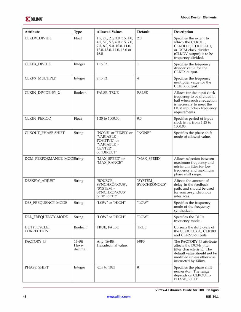
Attribute Type Allowed Values Default Description
CLK_FEEDBACK String "1X" , "2X", or "NONE" “1X” Specifies the clock feedbackof the allowed value.
Vir tex-4 Libraries Guide for HDL Designs
ISE 10.1 www.xilinx.com 45
About Design Elements
Attribute Type Allowed Values Default Description
CLKDV_DIVIDE Float 1.5, 2.0, 2.5, 3.0, 3.5, 4.0,4.5, 5.0, 5.5, 6.0, 6.5, 7.0,7.5, 8.0, 9.0, 10.0, 11.0,12.0, 13.0, 14.0, 15.0 or16.0
2.0 Specifies the extent towhich the CLKDLL,CLKDLLE, CLKDLLHF,or DCM clock divider(CLKDV output) is to befrequency divided.
CLKFX_DIVIDE Integer 1 to 32 1 Specifies the frequencydivider value for theCLKFX output.
CLKFX_MULTIPLY Integer 2 to 32 4 Specifies the frequencymultiplier value for theCLKFX output.
CLKIN_DIVIDE-BY_2 Boolean FALSE, TRUE FALSE Allows for the input clockfrequency to be divided inhalf when such a reductionis necessary to meet theDCM input clock frequencyrequirements.
CLKIN_PERIOD Float 1.25 to 1000.00 0.0 Specifies period of inputclock in ns from 1.25 to1000.00.
CLKOUT_PHASE-SHIFT String "NONE" or "FIXED" or"VARIABLE_-POSITIVE" or"VARIABLE_-CENTER"or "DIRECT"
"NONE” Specifies the phase shiftmode of allowed value.
DCM_PERFORMANCE_MODEString "MAX_SPEED" or"MAX_RANGE”
"MAX_SPEED” Allows selection betweenmaximum frequency andminimum jitter for lowfrequency and maximumphase shift range.
DESKEW_ADJUST String "SOURCE_-SYNCHRONOUS","SYSTEM_-SYNCHRONOUS"or "0" to "15”
"SYSTEM_-SYNCHRONOUS"
Affects the amount ofdelay in the feedbackpath, and should be usedfor source-synchronousinterfaces.
DFS_FREQUENCY-MODE String "LOW" or "HIGH” "LOW” Specifies the frequencymode of the frequencysynthesizer.
DLL_FREQUENCY-MODE String "LOW" or "HIGH” "LOW” Specifies the DLL’sfrequency mode.
DUTY_CYCLE_CORRECTION
Boolean TRUE, FALSE TRUE Corrects the duty cycle ofthe CLK0, CLK90, CLK180,and CLK270 outputs.
FACTORY_JF 16-BitHexa-decimal
Any 16-BitHexadecimal value.
F0F0 The FACTORY_JF attributeaffects the DCMs jitterfilter characteristic. Thedefault value should not bemodified unless otherwiseinstructed by Xilinx.
PHASE_SHIFT Integer -255 to 1023 0 Specifies the phase shiftnumerator. The rangedepends on CLKOUT_-PHASE_SHIFT.
Vir tex-4 Libraries Guide for HDL Designs
46 www.xilinx.com ISE 10.1
About Design Elements
Attribute Type Allowed Values Default Description
SIM_DEVICE String “VIRTEX4”,“VIRTEX5”
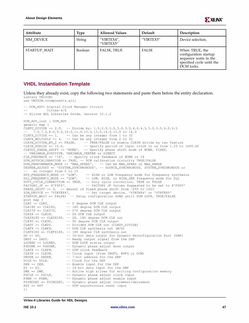
“VIRTEX5” Device selection.
STARTUP_WAIT Boolean FALSE, TRUE FALSE When TRUE, theconfiguration startupsequence waits in thespecified cycle until theDCM locks.
VHDL Instantiation Template
Unless they already exist, copy the following two statements and paste them before the entity declaration.Library UNISIM;use UNISIM.vcomponents.all;
-- DCM_ADV: Digital Clock Manager Circuit-- Virtex-4/5-- Xilinx HDL Libraries Guide, version 10.1.2
DCM_ADV_inst : DCM_ADVgeneric map (CLKDV_DIVIDE => 2.0, -- Divide by: 1.5,2.0,2.5,3.0,3.5,4.0,4.5,5.0,5.5,6.0,6.5-- 7.0,7.5,8.0,9.0,10.0,11.0,12.0,13.0,14.0,15.0 or 16.0CLKFX_DIVIDE => 1, -- Can be any integer from 1 to 32CLKFX_MULTIPLY => 4, -- Can be any integer from 2 to 32CLKIN_DIVIDE_BY_2 => FALSE, -- TRUE/FALSE to enable CLKIN divide by two featureCLKIN_PERIOD => 10.0, -- Specify period of input clock in ns from 1.25 to 1000.00CLKOUT_PHASE_SHIFT=> "NONE", -- Specify phase shift mode of NONE, FIXED,-- VARIABLE_POSITIVE, VARIABLE_CENTERor DIRECTCLK_FEEDBACK=> "1X", -- Specify clock feedback of NONEor 1XDCM_AUTOCALIBRATION=> TRUE, -- DCMcalibration circuitry TRUE/FALSEDCM_PERFORMANCE_MODE=> "MAX_SPEED", -- Can be MAX_SPEEDor MAX_RANGEDESKEW_ADJUST=> "SYSTEM_SYNCHRONOUS",-- SOURCE_SYNCHRONOUS,SYSTEM_SYNCHRONOUSor-- an integer from 0 to 15DFS_FREQUENCY_MODE=> "LOW", -- HIGH or LOWfrequency mode for frequency synthesisDLL_FREQUENCY_MODE=> "LOW", -- LOW, HIGH, or HIGH_SER frequency mode for DLLDUTY_CYCLE_CORRECTION=> TRUE, -- Duty cycle correction, TRUE or FALSEFACTORY_JF=> X"F0F0", -- FACTORYJF Values Suggested to be set to X"F0F0"PHASE_SHIFT => 0, -- Amount of fixed phase shift from -255 to 1023SIM_DEVICE => "VIRTEX4", -- Set target device, "VIRTEX4" or "VIRTEX5"STARTUP_WAIT=> FALSE) -- Delay configuration DONEuntil DCMLOCK, TRUE/FALSEport map (CLK0 => CLK0, -- 0 degree DCMCLK outputCLK180 => CLK180, -- 180 degree DCMCLK outputCLK270 => CLK270, -- 270 degree DCMCLK outputCLK2X => CLK2X, -- 2X DCMCLK outputCLK2X180 => CLK2X180, -- 2X, 180 degree DCMCLK outCLK90 => CLK90, -- 90 degree DCMCLK outputCLKDV => CLKDV, -- Divided DCMCLK out (CLKDV_DIVIDE)CLKFX => CLKFX, -- DCMCLK synthesis out (M/D)CLKFX180 => CLKFX180, -- 180 degree CLK synthesis outDO => DO, -- 16-bit data output for Dynamic Reconfiguration Port (DRP)DRDY=> DRDY, -- Ready output signal from the DRPLOCKED=> LOCKED, -- DCMLOCK status outputPSDONE=> PSDONE, -- Dynamic phase adjust done outputCLKFB => CLKFB, -- DCMclock feedbackCLKIN => CLKIN, -- Clock input (from IBUFG, BUFG or DCM)DADDR=> DADDR, -- 7-bit address for the DRPDCLK => DCLK, -- Clock for the DRPDEN => DEN, -- Enable input for the DRPDI => DI, -- 16-bit data input for the DRPDWE=> DWE, -- Active high allows for writing configuration memoryPSCLK => PSCLK, -- Dynamic phase adjust clock inputPSEN => PSEN, -- Dynamic phase adjust enable inputPSINCDEC => PSINCDEC, -- Dynamic phase adjust increment/decrementRST => RST -- DCMasynchronous reset input);
Vir tex-4 Libraries Guide for HDL Designs
ISE 10.1 www.xilinx.com 47
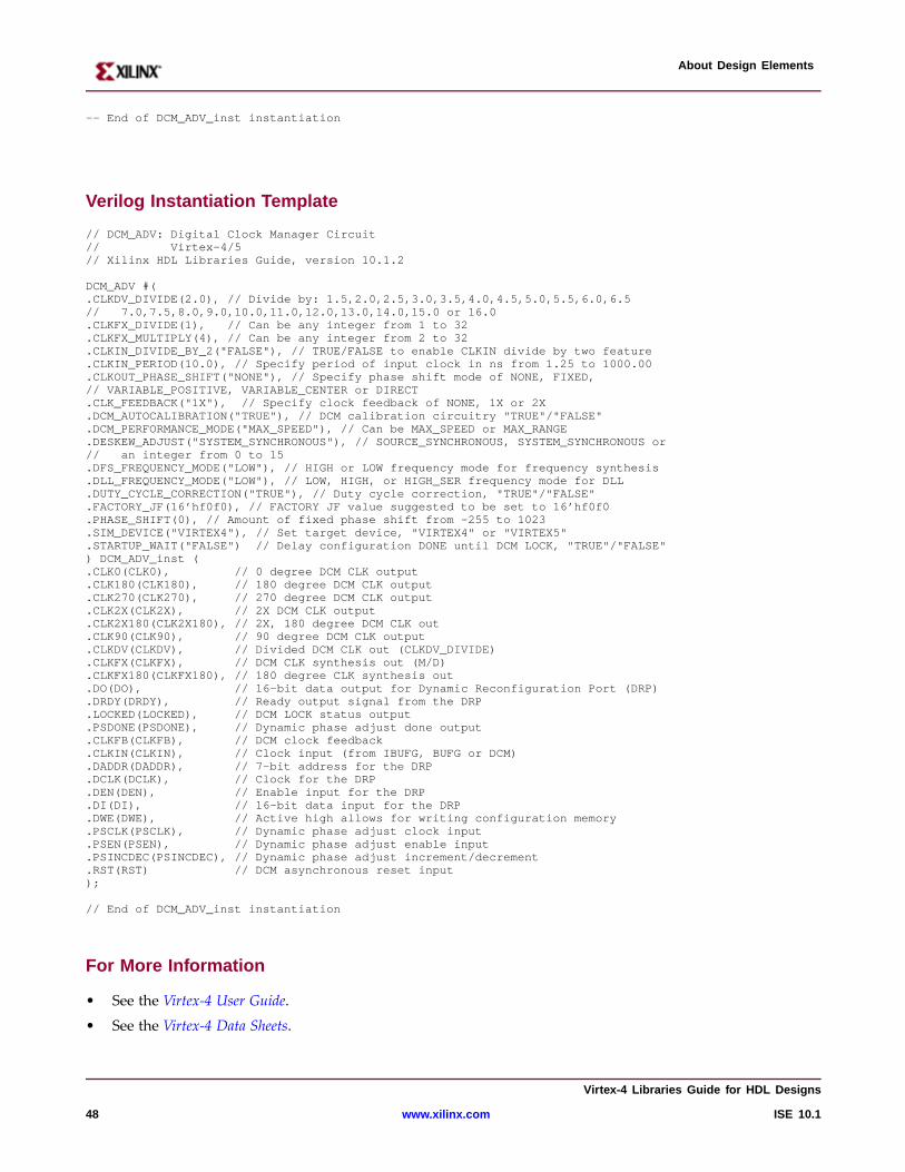
About Design Elements
-- End of DCM_ADV_inst instantiation
Verilog Instantiation Template
// DCM_ADV: Digital Clock Manager Circuit// Virtex-4/5// Xilinx HDL Libraries Guide, version 10.1.2
DCM_ADV#(.CLKDV_DIVIDE(2.0), // Divide by: 1.5,2.0,2.5,3.0,3.5,4.0,4.5,5.0,5.5,6.0,6.5// 7.0,7.5,8.0,9.0,10.0,11.0,12.0,13.0,14.0,15.0 or 16.0.CLKFX_DIVIDE(1), // Can be any integer from 1 to 32.CLKFX_MULTIPLY(4), // Can be any integer from 2 to 32.CLKIN_DIVIDE_BY_2("FALSE"), // TRUE/FALSE to enable CLKIN divide by two feature.CLKIN_PERIOD(10.0), // Specify period of input clock in ns from 1.25 to 1000.00.CLKOUT_PHASE_SHIFT("NONE"), // Specify phase shift mode of NONE, FIXED,// VARIABLE_POSITIVE, VARIABLE_CENTERor DIRECT.CLK_FEEDBACK("1X"), // Specify clock feedback of NONE, 1X or 2X.DCM_AUTOCALIBRATION("TRUE"), // DCMcalibration circuitry "TRUE"/"FALSE".DCM_PERFORMANCE_MODE("MAX_SPEED"),// Can be MAX_SPEEDor MAX_RANGE.DESKEW_ADJUST("SYSTEM_SYNCHRONOUS"),// SOURCE_SYNCHRONOUS,SYSTEM_SYNCHRONOUSor// an integer from 0 to 15.DFS_FREQUENCY_MODE("LOW"), // HIGH or LOWfrequency mode for frequency synthesis.DLL_FREQUENCY_MODE("LOW"), // LOW, HIGH, or HIGH_SER frequency mode for DLL.DUTY_CYCLE_CORRECTION("TRUE"), // Duty cycle correction, "TRUE"/"FALSE".FACTORY_JF(16’hf0f0), // FACTORYJF value suggested to be set to 16’hf0f0.PHASE_SHIFT(0), // Amount of fixed phase shift from -255 to 1023.SIM_DEVICE("VIRTEX4"), // Set target device, "VIRTEX4" or "VIRTEX5".STARTUP_WAIT("FALSE") // Delay configuration DONEuntil DCMLOCK, "TRUE"/"FALSE") DCM_ADV_inst (.CLK0(CLK0), // 0 degree DCMCLK output.CLK180(CLK180), // 180 degree DCMCLK output.CLK270(CLK270), // 270 degree DCMCLK output.CLK2X(CLK2X), // 2X DCMCLK output.CLK2X180(CLK2X180), // 2X, 180 degree DCMCLK out.CLK90(CLK90), // 90 degree DCMCLK output.CLKDV(CLKDV), // Divided DCMCLK out (CLKDV_DIVIDE).CLKFX(CLKFX), // DCMCLK synthesis out (M/D).CLKFX180(CLKFX180), // 180 degree CLK synthesis out.DO(DO), // 16-bit data output for Dynamic Reconfiguration Port (DRP).DRDY(DRDY), // Ready output signal from the DRP.LOCKED(LOCKED), // DCMLOCK status output.PSDONE(PSDONE), // Dynamic phase adjust done output.CLKFB(CLKFB), // DCMclock feedback.CLKIN(CLKIN), // Clock input (from IBUFG, BUFG or DCM).DADDR(DADDR), // 7-bit address for the DRP.DCLK(DCLK), // Clock for the DRP.DEN(DEN), // Enable input for the DRP.DI(DI), // 16-bit data input for the DRP.DWE(DWE), // Active high allows for writing configuration memory.PSCLK(PSCLK), // Dynamic phase adjust clock input.PSEN(PSEN), // Dynamic phase adjust enable input.PSINCDEC(PSINCDEC), // Dynamic phase adjust increment/decrement.RST(RST) // DCMasynchronous reset input);
// End of DCM_ADV_inst instantiation
For More Information
• See the Virtex-4 User Guide.
• See the Virtex-4 Data Sheets.
Vir tex-4 Libraries Guide for HDL Designs
48 www.xilinx.com ISE 10.1
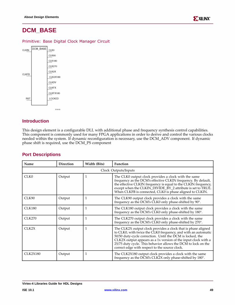
About Design Elements
DCM_BASE
Primitive: Base Digital Clock Manager Circuit
Intr oduction
This design element is a configurable DLL with additional phase and frequency synthesis control capabilities.This component is commonly used for many FPGA applications in order to derive and control the various clocksneeded within the system. If dynamic reconfiguration is necessary, use the DCM_ADV component. If dynamicphase shift is required, use the DCM_PS component
Por t Descriptions
Name Direction Width (Bits) Function
Clock Outputs/Inputs
CLK0 Output 1 The CLK0 output clock provides a clock with the samefrequency as the DCM’s effective CLKIN frequency. By default,the effective CLKIN frequency is equal to the CLKIN frequency,except when the CLKIN_DIVIDE_BY_2 attribute is set to TRUE.When CLKFB is connected, CLK0 is phase aligned to CLKIN.
CLK90 Output 1 The CLK90 output clock provides a clock with the samefrequency as the DCM’s CLK0 only phase-shifted by 90°.
CLK180 Output 1 The CLK180 output clock provides a clock with the samefrequency as the DCM’s CLK0 only phase-shifted by 180°.
CLK270 Output 1 The CLK270 output clock provides a clock with the samefrequency as the DCM’s CLK0 only phase-shifted by 270°.
CLK2X Output 1 The CLK2X output clock provides a clock that is phase alignedto CLK0, with twice the CLK0 frequency, and with an automatic50/50 duty-cycle correction. Until the DCM is locked, theCLK2X output appears as a 1x version of the input clock with a25/75 duty cycle. This behavior allows the DCM to lock on thecorrect edge with respect to the source clock.
CLK2X180 Output 1 The CLK2X180 output clock provides a clock with the samefrequency as the DCM’s CLK2X only phase-shifted by 180°.
Vir tex-4 Libraries Guide for HDL Designs
ISE 10.1 www.xilinx.com 49
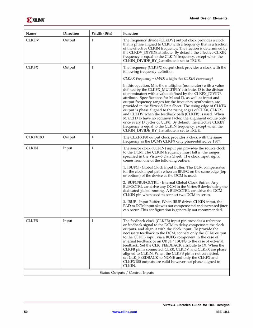
About Design Elements
Name Direction Width (Bits) Function
CLKDV Output 1 The frequency divide (CLKDV) output clock provides a clockthat is phase aligned to CLK0 with a frequency that is a fractionof the effective CLKIN frequency. The fraction is determined bythe CLKDV_DIVIDE attribute. By default, the effective CLKINfrequency is equal to the CLKIN frequency, except when theCLKIN_DIVIDE_BY_2 attribute is set to TRUE.
CLKFX Output 1 The frequency (CLKFX) output clock provides a clock with thefollowing frequency definition:
CLKFX Frequency = (M/D) x (Effective CLKIN Frequency)
In this equation, M is the multiplier (numerator) with a valuedefined by the CLKFX_MULTIPLY attribute. D is the divisor(denominator) with a value defined by the CLKFX_DIVIDEattribute. Specifications for M and D, as well as input andoutput frequency ranges for the frequency synthesizer, areprovided in the Virtex-5 Data Sheet. The rising edge of CLKFXoutput is phase aligned to the rising edges of CLK0, CLK2X,and CLKDV when the feedback path (CLKFB) is used. WhenM and D to have no common factor, the alignment occurs onlyonce every D cycles of CLK0. By default, the effective CLKINfrequency is equal to the CLKIN frequency, except when theCLKIN_DIVIDE_BY_2 attribute is set to TRUE.
CLKFX180 Output 1 The CLKFX180 output clock provides a clock with the samefrequency as the DCM’s CLKFX only phase-shifted by 180°.
CLKIN Input 1 The source clock (CLKIN) input pin provides the source clockto the DCM. The CLKIN frequency must fall in the rangesspecified in the Virtex-5 Data Sheet. The clock input signalcomes from one of the following buffers:
1. IBUFG - Global Clock Input Buffer. The DCM compensatesfor the clock input path when an IBUFG on the same edge (topor bottom) of the device as the DCM is used.
2. BUFG/BUFGCTRL - Internal Global Clock Buffer. AnyBUFGCTRL can drive any DCM in the Virtex-5 device using thededicated global routing. A BUFGCTRL can drive the DCMCLKIN pin when used to connect two DCM in series.
3. IBUF - Input Buffer. When IBUF drives CLKIN input, thePAD to DCM input skew is not compensated and increased jittercan occur. This configuration is generally not recommended.
CLKFB Input 1 The feedback clock (CLKFB) input pin provides a referenceor feedback signal to the DCM to delay-compensate the clockoutputs, and align it with the clock input. To provide thenecessary feedback to the DCM, connect only the CLK0 outputto the CLKFB input via a BUFG component in the case ofinternal feedback or an OBUF ’ IBUFG to the case of externalfeedback. Set the CLK_FEEDBACK attribute to 1X. When theCLKFB pin is connected, CLK0, CLKDV, and CLKFX are phasealigned to CLKIN. When the CLKFB pin is not connected,set CLK_FEEDBACK to NONE and only the CLKFX andCLKFX180 outputs are valid however not phase aligned toCLKIN.
Status Outputs / Control Inputs
Vir tex-4 Libraries Guide for HDL Designs
50 www.xilinx.com ISE 10.1
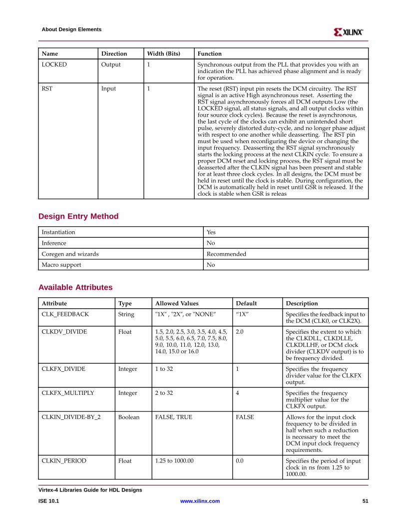
About Design Elements
Name Direction Width (Bits) Function
LOCKED Output 1 Synchronous output from the PLL that provides you with anindication the PLL has achieved phase alignment and is readyfor operation.
RST Input 1 The reset (RST) input pin resets the DCM circuitry. The RSTsignal is an active High asynchronous reset. Asserting theRST signal asynchronously forces all DCM outputs Low (theLOCKED signal, all status signals, and all output clocks withinfour source clock cycles). Because the reset is asynchronous,the last cycle of the clocks can exhibit an unintended shortpulse, severely distorted duty-cycle, and no longer phase adjustwith respect to one another while deasserting. The RST pinmust be used when reconfiguring the device or changing theinput frequency. Deasserting the RST signal synchronouslystarts the locking process at the next CLKIN cycle. To ensure aproper DCM reset and locking process, the RST signal must bedeasserted after the CLKIN signal has been present and stablefor at least three clock cycles. In all designs, the DCM must beheld in reset until the clock is stable. During configuration, theDCM is automatically held in reset until GSR is released. If theclock is stable when GSR is releas
Design Entr y Method
Instantiation Yes
Inference No
Coregen and wizards Recommended
Macro support No
Availab le Attrib utes
Attribute Type Allowed Values Default Description
CLK_FEEDBACK String "1X" , "2X", or "NONE” “1X” Specifies the feedback input tothe DCM (CLK0, or CLK2X).
CLKDV_DIVIDE Float 1.5, 2.0, 2.5, 3.0, 3.5, 4.0, 4.5,5.0, 5.5, 6.0, 6.5, 7.0, 7.5, 8.0,9.0, 10.0, 11.0, 12.0, 13.0,14.0, 15.0 or 16.0
2.0 Specifies the extent to whichthe CLKDLL, CLKDLLE,CLKDLLHF, or DCM clockdivider (CLKDV output) is tobe frequency divided.
CLKFX_DIVIDE Integer 1 to 32 1 Specifies the frequencydivider value for the CLKFXoutput.
CLKFX_MULTIPLY Integer 2 to 32 4 Specifies the frequencymultiplier value for theCLKFX output.
CLKIN_DIVIDE-BY_2 Boolean FALSE, TRUE FALSE Allows for the input clockfrequency to be divided inhalf when such a reductionis necessary to meet theDCM input clock frequencyrequirements.
CLKIN_PERIOD Float 1.25 to 1000.00 0.0 Specifies the period of inputclock in ns from 1.25 to1000.00.
Vir tex-4 Libraries Guide for HDL Designs
ISE 10.1 www.xilinx.com 51
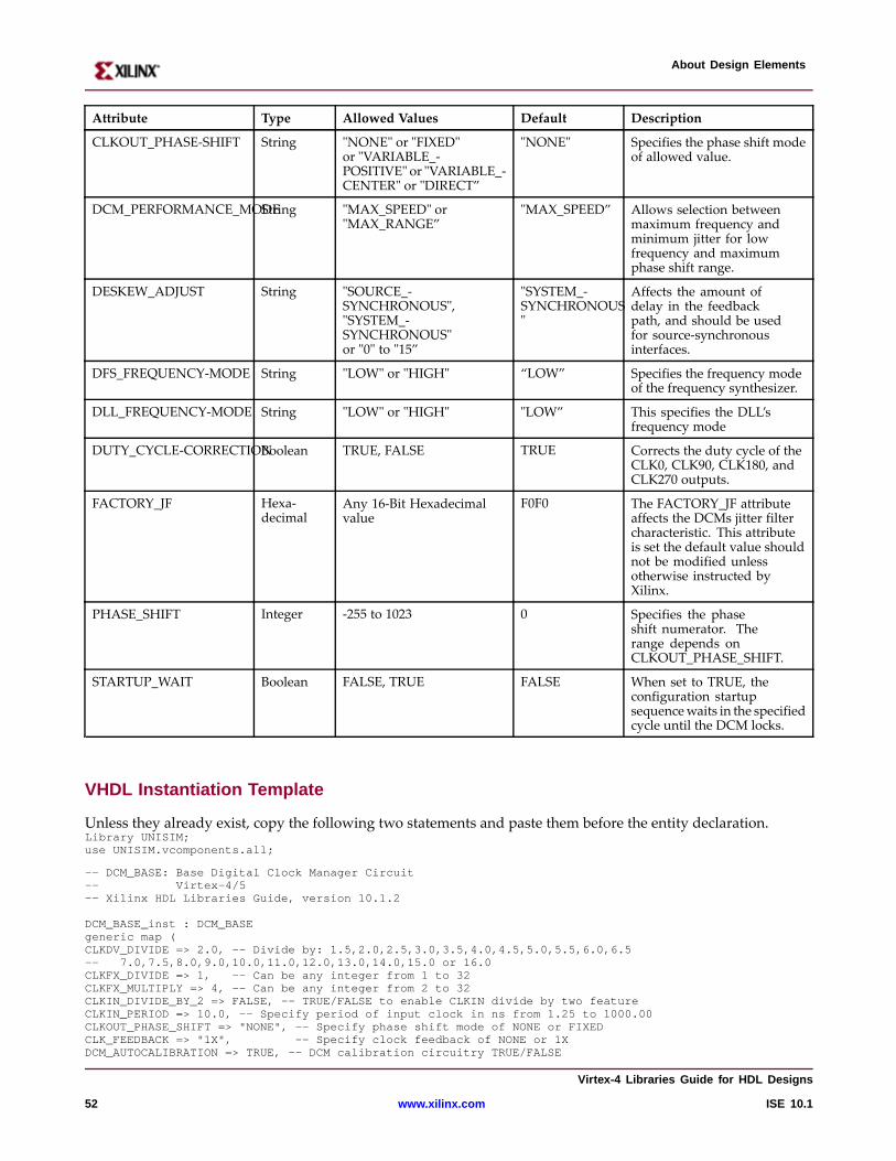
About Design Elements
Attribute Type Allowed Values Default Description
CLKOUT_PHASE-SHIFT String "NONE" or "FIXED"or "VARIABLE_-POSITIVE" or "VARIABLE_-CENTER" or "DIRECT”
"NONE" Specifies the phase shift modeof allowed value.
DCM_PERFORMANCE_MODEString "MAX_SPEED" or"MAX_RANGE”
"MAX_SPEED” Allows selection betweenmaximum frequency andminimum jitter for lowfrequency and maximumphase shift range.
DESKEW_ADJUST String "SOURCE_-SYNCHRONOUS","SYSTEM_-SYNCHRONOUS"or "0" to "15”
"SYSTEM_-SYNCHRONOUS"
Affects the amount ofdelay in the feedbackpath, and should be usedfor source-synchronousinterfaces.
DFS_FREQUENCY-MODE String "LOW" or "HIGH" “LOW” Specifies the frequency modeof the frequency synthesizer.
DLL_FREQUENCY-MODE String "LOW" or "HIGH" "LOW” This specifies the DLL’sfrequency mode
DUTY_CYCLE-CORRECTIONBoolean TRUE, FALSE TRUE Corrects the duty cycle of theCLK0, CLK90, CLK180, andCLK270 outputs.
FACTORY_JF Hexa-decimal
Any 16-Bit Hexadecimalvalue
F0F0 The FACTORY_JF attributeaffects the DCMs jitter filtercharacteristic. This attributeis set the default value shouldnot be modified unlessotherwise instructed byXilinx.
PHASE_SHIFT Integer -255 to 1023 0 Specifies the phaseshift numerator. Therange depends onCLKOUT_PHASE_SHIFT.
STARTUP_WAIT Boolean FALSE, TRUE FALSE When set to TRUE, theconfiguration startupsequencewaits in the specifiedcycle until the DCM locks.
VHDL Instantiation Template
Unless they already exist, copy the following two statements and paste them before the entity declaration.Library UNISIM;use UNISIM.vcomponents.all;
-- DCM_BASE: Base Digital Clock Manager Circuit-- Virtex-4/5-- Xilinx HDL Libraries Guide, version 10.1.2
DCM_BASE_inst : DCM_BASEgeneric map (CLKDV_DIVIDE => 2.0, -- Divide by: 1.5,2.0,2.5,3.0,3.5,4.0,4.5,5.0,5.5,6.0,6.5-- 7.0,7.5,8.0,9.0,10.0,11.0,12.0,13.0,14.0,15.0 or 16.0CLKFX_DIVIDE => 1, -- Can be any integer from 1 to 32CLKFX_MULTIPLY => 4, -- Can be any integer from 2 to 32CLKIN_DIVIDE_BY_2 => FALSE, -- TRUE/FALSE to enable CLKIN divide by two featureCLKIN_PERIOD => 10.0, -- Specify period of input clock in ns from 1.25 to 1000.00CLKOUT_PHASE_SHIFT=> "NONE", -- Specify phase shift mode of NONEor FIXEDCLK_FEEDBACK=> "1X", -- Specify clock feedback of NONEor 1XDCM_AUTOCALIBRATION=> TRUE, -- DCMcalibration circuitry TRUE/FALSE
Vir tex-4 Libraries Guide for HDL Designs
52 www.xilinx.com ISE 10.1
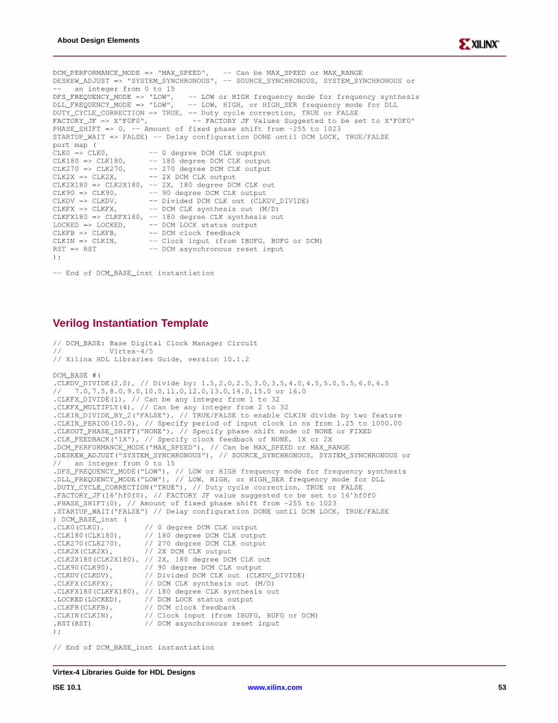
About Design Elements
DCM_PERFORMANCE_MODE=> "MAX_SPEED", -- Can be MAX_SPEEDor MAX_RANGEDESKEW_ADJUST=> "SYSTEM_SYNCHRONOUS",-- SOURCE_SYNCHRONOUS,SYSTEM_SYNCHRONOUSor-- an integer from 0 to 15DFS_FREQUENCY_MODE=> "LOW", -- LOWor HIGH frequency mode for frequency synthesisDLL_FREQUENCY_MODE=> "LOW", -- LOW, HIGH, or HIGH_SER frequency mode for DLLDUTY_CYCLE_CORRECTION=> TRUE, -- Duty cycle correction, TRUE or FALSEFACTORY_JF=> X"F0F0", -- FACTORYJF Values Suggested to be set to X"F0F0"PHASE_SHIFT => 0, -- Amount of fixed phase shift from -255 to 1023STARTUP_WAIT=> FALSE) -- Delay configuration DONEuntil DCMLOCK, TRUE/FALSEport map (CLK0 => CLK0, -- 0 degree DCMCLK ouptputCLK180 => CLK180, -- 180 degree DCMCLK outputCLK270 => CLK270, -- 270 degree DCMCLK outputCLK2X => CLK2X, -- 2X DCMCLK outputCLK2X180 => CLK2X180, -- 2X, 180 degree DCMCLK outCLK90 => CLK90, -- 90 degree DCMCLK outputCLKDV => CLKDV, -- Divided DCMCLK out (CLKDV_DIVIDE)CLKFX => CLKFX, -- DCMCLK synthesis out (M/D)CLKFX180 => CLKFX180, -- 180 degree CLK synthesis outLOCKED=> LOCKED, -- DCMLOCK status outputCLKFB => CLKFB, -- DCMclock feedbackCLKIN => CLKIN, -- Clock input (from IBUFG, BUFG or DCM)RST => RST -- DCMasynchronous reset input);
-- End of DCM_BASE_inst instantiation
Verilog Instantiation Template
// DCM_BASE: Base Digital Clock Manager Circuit// Virtex-4/5// Xilinx HDL Libraries Guide, version 10.1.2
DCM_BASE#(.CLKDV_DIVIDE(2.0), // Divide by: 1.5,2.0,2.5,3.0,3.5,4.0,4.5,5.0,5.5,6.0,6.5// 7.0,7.5,8.0,9.0,10.0,11.0,12.0,13.0,14.0,15.0 or 16.0.CLKFX_DIVIDE(1), // Can be any integer from 1 to 32.CLKFX_MULTIPLY(4), // Can be any integer from 2 to 32.CLKIN_DIVIDE_BY_2("FALSE"), // TRUE/FALSE to enable CLKIN divide by two feature.CLKIN_PERIOD(10.0), // Specify period of input clock in ns from 1.25 to 1000.00.CLKOUT_PHASE_SHIFT("NONE"), // Specify phase shift mode of NONEor FIXED.CLK_FEEDBACK("1X"), // Specify clock feedback of NONE, 1X or 2X.DCM_PERFORMANCE_MODE("MAX_SPEED"),// Can be MAX_SPEEDor MAX_RANGE.DESKEW_ADJUST("SYSTEM_SYNCHRONOUS"),// SOURCE_SYNCHRONOUS,SYSTEM_SYNCHRONOUSor// an integer from 0 to 15.DFS_FREQUENCY_MODE("LOW"), // LOWor HIGH frequency mode for frequency synthesis.DLL_FREQUENCY_MODE("LOW"), // LOW, HIGH, or HIGH_SER frequency mode for DLL.DUTY_CYCLE_CORRECTION("TRUE"), // Duty cycle correction, TRUE or FALSE.FACTORY_JF(16’hf0f0), // FACTORYJF value suggested to be set to 16’hf0f0.PHASE_SHIFT(0), // Amount of fixed phase shift from -255 to 1023.STARTUP_WAIT("FALSE") // Delay configuration DONEuntil DCMLOCK, TRUE/FALSE) DCM_BASE_inst (.CLK0(CLK0), // 0 degree DCMCLK output.CLK180(CLK180), // 180 degree DCMCLK output.CLK270(CLK270), // 270 degree DCMCLK output.CLK2X(CLK2X), // 2X DCMCLK output.CLK2X180(CLK2X180), // 2X, 180 degree DCMCLK out.CLK90(CLK90), // 90 degree DCMCLK output.CLKDV(CLKDV), // Divided DCMCLK out (CLKDV_DIVIDE).CLKFX(CLKFX), // DCMCLK synthesis out (M/D).CLKFX180(CLKFX180), // 180 degree CLK synthesis out.LOCKED(LOCKED), // DCMLOCK status output.CLKFB(CLKFB), // DCMclock feedback.CLKIN(CLKIN), // Clock input (from IBUFG, BUFG or DCM).RST(RST) // DCMasynchronous reset input);
// End of DCM_BASE_inst instantiation
Vir tex-4 Libraries Guide for HDL Designs
ISE 10.1 www.xilinx.com 53
About Design Elements
For More Information
• See the Virtex-4 User Guide.
• See the Virtex-4 Data Sheets.
Vir tex-4 Libraries Guide for HDL Designs
54 www.xilinx.com ISE 10.1
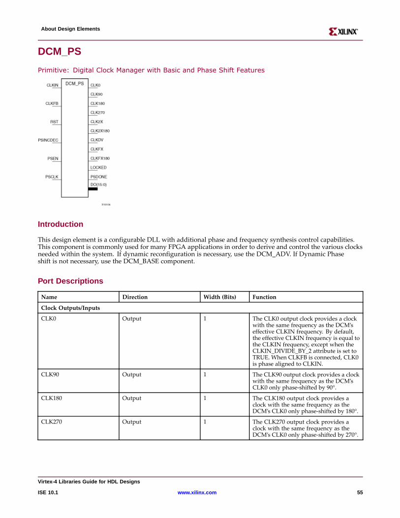
About Design Elements
DCM_PS
Primitive: Digital Clock Manager with Basic and Phase Shift Features
Intr oduction
This design element is a configurable DLL with additional phase and frequency synthesis control capabilities.This component is commonly used for many FPGA applications in order to derive and control the various clocksneeded within the system. If dynamic reconfiguration is necessary, use the DCM_ADV. If Dynamic Phaseshift is not necessary, use the DCM_BASE component.
Por t Descriptions
Name Direction Width (Bits) Function
Clock Outputs/Inputs
CLK0 Output 1 The CLK0 output clock provides a clockwith the same frequency as the DCM’seffective CLKIN frequency. By default,the effective CLKIN frequency is equal tothe CLKIN frequency, except when theCLKIN_DIVIDE_BY_2 attribute is set toTRUE. When CLKFB is connected, CLK0is phase aligned to CLKIN.
CLK90 Output 1 The CLK90 output clock provides a clockwith the same frequency as the DCM’sCLK0 only phase-shifted by 90°.
CLK180 Output 1 The CLK180 output clock provides aclock with the same frequency as theDCM’s CLK0 only phase-shifted by 180°.
CLK270 Output 1 The CLK270 output clock provides aclock with the same frequency as theDCM’s CLK0 only phase-shifted by 270°.
Vir tex-4 Libraries Guide for HDL Designs
ISE 10.1 www.xilinx.com 55
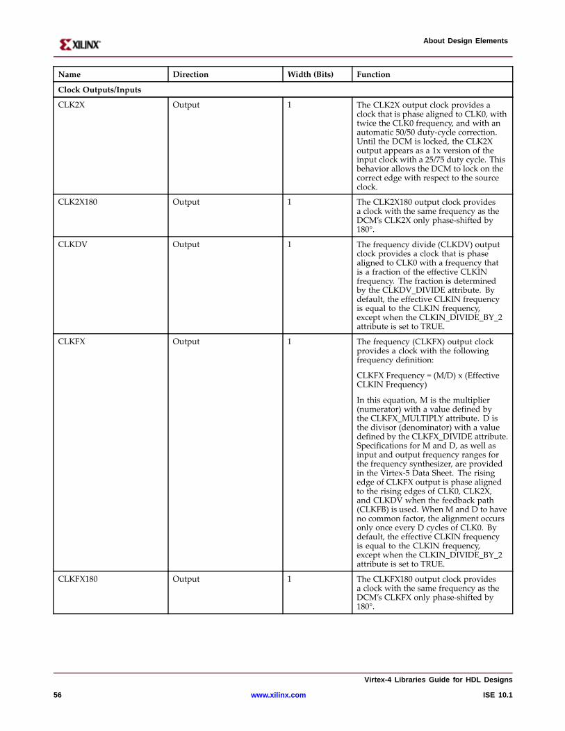
About Design Elements
Name Direction Width (Bits) Function
Clock Outputs/Inputs
CLK2X Output 1 The CLK2X output clock provides aclock that is phase aligned to CLK0, withtwice the CLK0 frequency, and with anautomatic 50/50 duty-cycle correction.Until the DCM is locked, the CLK2Xoutput appears as a 1x version of theinput clock with a 25/75 duty cycle. Thisbehavior allows the DCM to lock on thecorrect edge with respect to the sourceclock.
CLK2X180 Output 1 The CLK2X180 output clock providesa clock with the same frequency as theDCM’s CLK2X only phase-shifted by180°.
CLKDV Output 1 The frequency divide (CLKDV) outputclock provides a clock that is phasealigned to CLK0 with a frequency thatis a fraction of the effective CLKINfrequency. The fraction is determinedby the CLKDV_DIVIDE attribute. Bydefault, the effective CLKIN frequencyis equal to the CLKIN frequency,except when the CLKIN_DIVIDE_BY_2attribute is set to TRUE.
CLKFX Output 1 The frequency (CLKFX) output clockprovides a clock with the followingfrequency definition:
CLKFX Frequency = (M/D) x (EffectiveCLKIN Frequency)
In this equation, M is the multiplier(numerator) with a value defined bythe CLKFX_MULTIPLY attribute. D isthe divisor (denominator) with a valuedefined by the CLKFX_DIVIDE attribute.Specifications for M and D, as well asinput and output frequency ranges forthe frequency synthesizer, are providedin the Virtex-5 Data Sheet. The risingedge of CLKFX output is phase alignedto the rising edges of CLK0, CLK2X,and CLKDV when the feedback path(CLKFB) is used. When M and D to haveno common factor, the alignment occursonly once every D cycles of CLK0. Bydefault, the effective CLKIN frequencyis equal to the CLKIN frequency,except when the CLKIN_DIVIDE_BY_2attribute is set to TRUE.
CLKFX180 Output 1 The CLKFX180 output clock providesa clock with the same frequency as theDCM’s CLKFX only phase-shifted by180°.
Vir tex-4 Libraries Guide for HDL Designs
56 www.xilinx.com ISE 10.1
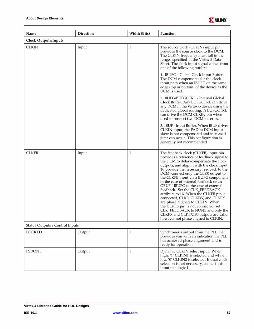
About Design Elements
Name Direction Width (Bits) Function
Clock Outputs/Inputs
CLKIN Input 1 The source clock (CLKIN) input pinprovides the source clock to the DCM.The CLKIN frequency must fall in theranges specified in the Virtex-5 DataSheet. The clock input signal comes fromone of the following buffers:
1. IBUFG - Global Clock Input Buffer.The DCM compensates for the clockinput path when an IBUFG on the sameedge (top or bottom) of the device as theDCM is used.
2. BUFG/BUFGCTRL - Internal GlobalClock Buffer. Any BUFGCTRL can driveany DCM in the Virtex-5 device using thededicated global routing. A BUFGCTRLcan drive the DCM CLKIN pin whenused to connect two DCM in series.
3. IBUF - Input Buffer. When IBUF drivesCLKIN input, the PAD to DCM inputskew is not compensated and increasedjitter can occur. This configuration isgenerally not recommended.
CLKFB Input 1 The feedback clock (CLKFB) input pinprovides a reference or feedback signal tothe DCM to delay-compensate the clockoutputs, and align it with the clock input.To provide the necessary feedback to theDCM, connect only the CLK0 output tothe CLKFB input via a BUFG componentin the case of internal feedback or anOBUF ’ IBUFG to the case of externalfeedback. Set the CLK_FEEDBACKattribute to 1X. When the CLKFB pin isconnected, CLK0, CLKDV, and CLKFXare phase aligned to CLKIN. Whenthe CLKFB pin is not connected, setCLK_FEEDBACK to NONE and only theCLKFX and CLKFX180 outputs are validhowever not phase aligned to CLKIN.
Status Outputs / Control Inputs
LOCKED Output 1 Synchronous output from the PLL thatprovides you with an indication the PLLhas achieved phase alignment and isready for operation.
PSDONE Output 1 Dynamic CLKIN select input. Whenhigh, ’1’ CLKIN1 is selected and whilelow, ’0’ CLKIN2 is selected. If dual clockselection is not necessary, connect thisinput to a logic 1.
Vir tex-4 Libraries Guide for HDL Designs
ISE 10.1 www.xilinx.com 57
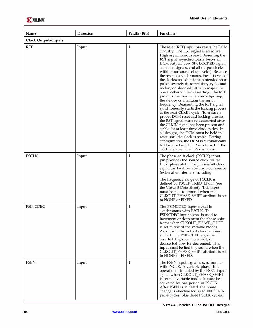
About Design Elements
Name Direction Width (Bits) Function
Clock Outputs/Inputs
RST Input 1 The reset (RST) input pin resets the DCMcircuitry. The RST signal is an activeHigh asynchronous reset. Asserting theRST signal asynchronously forces allDCM outputs Low (the LOCKED signal,all status signals, and all output clockswithin four source clock cycles). Becausethe reset is asynchronous, the last cycle ofthe clocks can exhibit an unintended shortpulse, severely distorted duty-cycle, andno longer phase adjust with respect toone another while deasserting. The RSTpin must be used when reconfiguringthe device or changing the inputfrequency. Deasserting the RST signalsynchronously starts the locking processat the next CLKIN cycle. To ensure aproper DCM reset and locking process,the RST signal must be deasserted afterthe CLKIN signal has been present andstable for at least three clock cycles. Inall designs, the DCM must be held inreset until the clock is stable. Duringconfiguration, the DCM is automaticallyheld in reset until GSR is released. If theclock is stable when GSR is releas
PSCLK Input 1 The phase-shift clock (PSCLK) inputpin provides the source clock for theDCM phase shift. The phase-shift clocksignal can be driven by any clock source(external or internal), including:
The frequency range of PSCLK isdefined by PSCLK_FREQ_LF/HF (seethe Virtex-5 Data Sheet). This inputmust be tied to ground when theCLKOUT_PHASE_SHIFT attribute is setto NONE or FIXED.
PSINCDEC Input 1 The PSINCDEC input signal issynchronous with PSCLK. ThePSINCDEC input signal is used toincrement or decrement the phase-shiftfactor when CLKOUT_PHASE_SHIFTis set to one of the variable modes.As a result, the output clock is phaseshifted. the PSINCDEC signal isasserted High for increment, ordeasserted Low for decrement. Thisinput must be tied to ground when theCLKOUT_PHASE_SHIFT attribute is setto NONE or FIXED.
PSEN Input 1 The PSEN input signal is synchronouswith PSCLK. A variable phase-shiftoperation is initiated by the PSEN inputsignal when CLKOUT_PHASE_SHIFTis set to a variable mode. It must beactivated for one period of PSCLK.After PSEN is initiated, the phasechange is effective for up to 100 CLKINpulse cycles, plus three PSCLK cycles,
Vir tex-4 Libraries Guide for HDL Designs
58 www.xilinx.com ISE 10.1
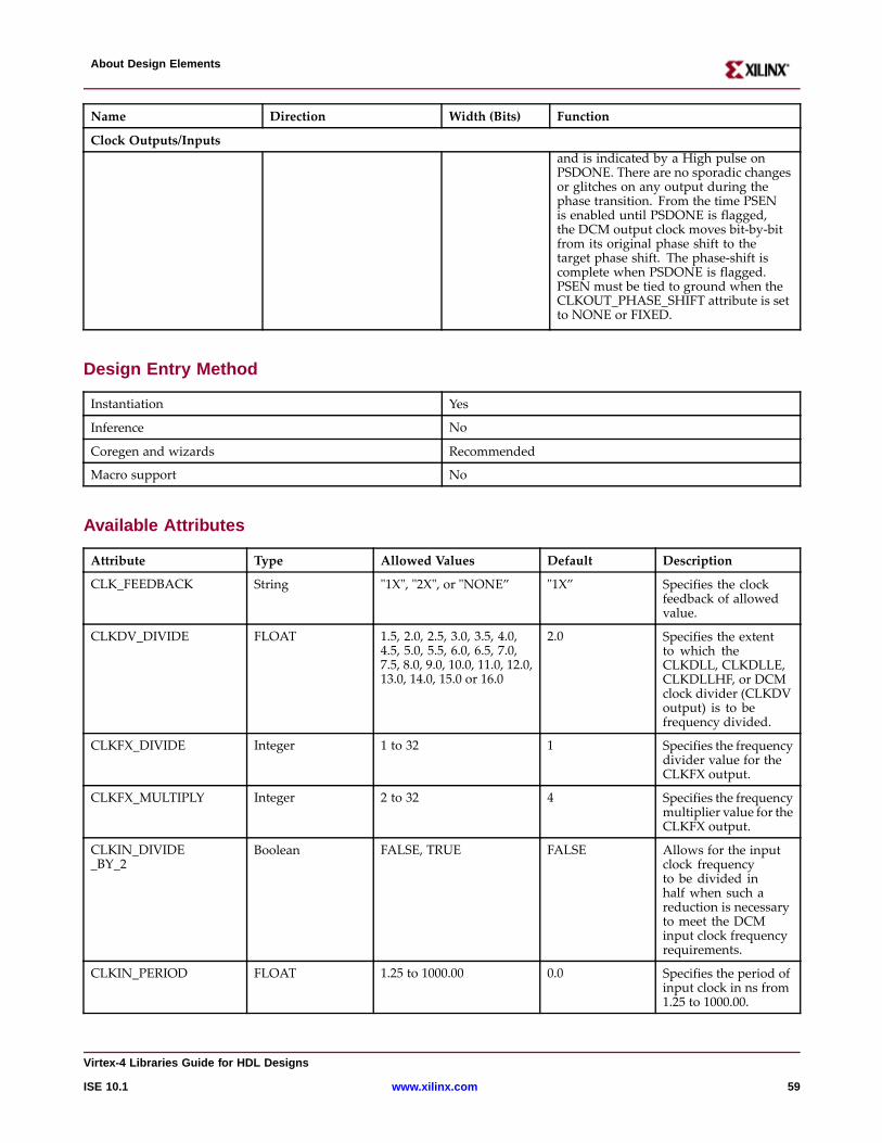
About Design Elements
Name Direction Width (Bits) Function
Clock Outputs/Inputsand is indicated by a High pulse onPSDONE. There are no sporadic changesor glitches on any output during thephase transition. From the time PSENis enabled until PSDONE is flagged,the DCM output clock moves bit-by-bitfrom its original phase shift to thetarget phase shift. The phase-shift iscomplete when PSDONE is flagged.PSEN must be tied to ground when theCLKOUT_PHASE_SHIFT attribute is setto NONE or FIXED.
Design Entr y Method
Instantiation Yes
Inference No
Coregen and wizards Recommended
Macro support No
Availab le Attrib utes
Attribute Type Allowed Values Default Description
CLK_FEEDBACK String "1X", "2X", or "NONE” "1X” Specifies the clockfeedback of allowedvalue.
CLKDV_DIVIDE FLOAT 1.5, 2.0, 2.5, 3.0, 3.5, 4.0,4.5, 5.0, 5.5, 6.0, 6.5, 7.0,7.5, 8.0, 9.0, 10.0, 11.0, 12.0,13.0, 14.0, 15.0 or 16.0
2.0 Specifies the extentto which theCLKDLL, CLKDLLE,CLKDLLHF, or DCMclock divider (CLKDVoutput) is to befrequency divided.
CLKFX_DIVIDE Integer 1 to 32 1 Specifies the frequencydivider value for theCLKFX output.
CLKFX_MULTIPLY Integer 2 to 32 4 Specifies the frequencymultiplier value for theCLKFX output.
CLKIN_DIVIDE_BY_2
Boolean FALSE, TRUE FALSE Allows for the inputclock frequencyto be divided inhalf when such areduction is necessaryto meet the DCMinput clock frequencyrequirements.
CLKIN_PERIOD FLOAT 1.25 to 1000.00 0.0 Specifies the period ofinput clock in ns from1.25 to 1000.00.
Vir tex-4 Libraries Guide for HDL Designs
ISE 10.1 www.xilinx.com 59
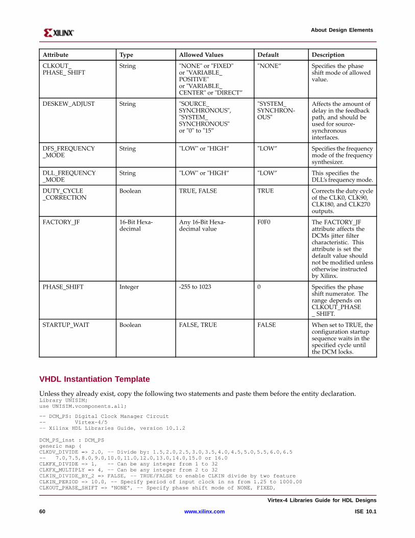
About Design Elements
Attribute Type Allowed Values Default Description
CLKOUT_PHASE_ SHIFT
String "NONE" or "FIXED"or "VARIABLE_POSITIVE"or "VARIABLE_CENTER" or "DIRECT”
"NONE” Specifies the phaseshift mode of allowedvalue.
DESKEW_ADJUST String "SOURCE_SYNCHRONOUS","SYSTEM_SYNCHRONOUS"or "0" to "15”
"SYSTEM_SYNCHRON-OUS"
Affects the amount ofdelay in the feedbackpath, and should beused for source-synchronousinterfaces.
DFS_FREQUENCY_MODE
String "LOW" or "HIGH” "LOW” Specifies the frequencymode of the frequencysynthesizer.
DLL_FREQUENCY_MODE
String "LOW" or "HIGH” "LOW” This specifies theDLL’s frequencymode.
DUTY_CYCLE_CORRECTION
Boolean TRUE, FALSE TRUE Corrects the duty cycleof the CLK0, CLK90,CLK180, and CLK270outputs.
FACTORY_JF 16-Bit Hexa-decimal
Any 16-Bit Hexa-decimal value
F0F0 The FACTORY_JFattribute affects theDCMs jitter filtercharacteristic. Thisattribute is set thedefault value shouldnot be modified unlessotherwise instructedby Xilinx.
PHASE_SHIFT Integer -255 to 1023 0 Specifies the phaseshift numerator. Therange depends onCLKOUT_PHASE_ SHIFT.
STARTUP_WAIT Boolean FALSE, TRUE FALSE When set to TRUE, theconfiguration startupsequence waits in thespecified cycle untilthe DCM locks.
VHDL Instantiation Template
Unless they already exist, copy the following two statements and paste them before the entity declaration.Library UNISIM;use UNISIM.vcomponents.all;
-- DCM_PS: Digital Clock Manager Circuit-- Virtex-4/5-- Xilinx HDL Libraries Guide, version 10.1.2
DCM_PS_inst : DCM_PSgeneric map (CLKDV_DIVIDE => 2.0, -- Divide by: 1.5,2.0,2.5,3.0,3.5,4.0,4.5,5.0,5.5,6.0,6.5-- 7.0,7.5,8.0,9.0,10.0,11.0,12.0,13.0,14.0,15.0 or 16.0CLKFX_DIVIDE => 1, -- Can be any integer from 1 to 32CLKFX_MULTIPLY => 4, -- Can be any integer from 2 to 32CLKIN_DIVIDE_BY_2 => FALSE, -- TRUE/FALSE to enable CLKIN divide by two featureCLKIN_PERIOD => 10.0, -- Specify period of input clock in ns from 1.25 to 1000.00CLKOUT_PHASE_SHIFT=> "NONE", -- Specify phase shift mode of NONE, FIXED,
Vir tex-4 Libraries Guide for HDL Designs
60 www.xilinx.com ISE 10.1
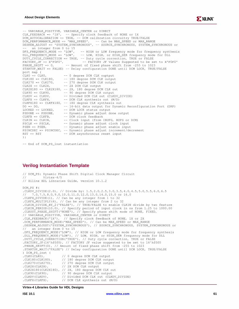
About Design Elements
-- VARIABLE_POSITIVE, VARIABLE_CENTERor DIRECTCLK_FEEDBACK=> "1X", -- Specify clock feedback of NONEor 1XDCM_AUTOCALIBRATION=> TRUE, -- DCMcalibration circuitry TRUE/FALSEDCM_PERFORMANCE_MODE=> "MAX_SPEED", -- Can be MAX_SPEEDor MAX_RANGEDESKEW_ADJUST=> "SYSTEM_SYNCHRONOUS",-- SOURCE_SYNCHRONOUS,SYSTEM_SYNCHRONOUSor-- an integer from 0 to 15DFS_FREQUENCY_MODE=> "LOW", -- HIGH or LOWfrequency mode for frequency synthesisDLL_FREQUENCY_MODE=> "LOW", -- LOW, HIGH, or HIGH_SER frequency mode for DLLDUTY_CYCLE_CORRECTION=> TRUE, -- Duty cycle correction, TRUE or FALSEFACTORY_JF=> X"F0F0", -- FACTORYJF Values Suggested to be set to X"F0F0"PHASE_SHIFT => 0, -- Amount of fixed phase shift from -255 to 1023STARTUP_WAIT=> FALSE) -- Delay configuration DONEuntil DCMLOCK, TRUE/FALSEport map (CLK0 => CLK0, -- 0 degree DCMCLK ouptputCLK180 => CLK180, -- 180 degree DCMCLK outputCLK270 => CLK270, -- 270 degree DCMCLK outputCLK2X => CLK2X, -- 2X DCMCLK outputCLK2X180 => CLK2X180, -- 2X, 180 degree DCMCLK outCLK90 => CLK90, -- 90 degree DCMCLK outputCLKDV => CLKDV, -- Divided DCMCLK out (CLKDV_DIVIDE)CLKFX => CLKFX, -- DCMCLK synthesis out (M/D)CLKFX180 => CLKFX180, -- 180 degree CLK synthesis outDO => DO, -- 16-bit data output for Dynamic Reconfiguration Port (DRP)LOCKED=> LOCKED, -- DCMLOCK status outputPSDONE=> PSDONE, -- Dynamic phase adjust done outputCLKFB => CLKFB, -- DCMclock feedbackCLKIN => CLKIN, -- Clock input (from IBUFG, BUFG or DCM)PSCLK => PSCLK, -- Dynamic phase adjust clock inputPSEN => PSEN, -- Dynamic phase adjust enable inputPSINCDEC => PSINCDEC, -- Dynamic phase adjust increment/decrementRST => RST -- DCMasynchronous reset input);
-- End of DCM_PS_inst instantiation
Verilog Instantiation Template
// DCM_PS: Dynamic Phase Shift Digital Clock Manager Circuit// Virtex-4/5// Xilinx HDL Libraries Guide, version 10.1.2
DCM_PS#(.CLKDV_DIVIDE(2.0), // Divide by: 1.5,2.0,2.5,3.0,3.5,4.0,4.5,5.0,5.5,6.0,6.5// 7.0,7.5,8.0,9.0,10.0,11.0,12.0,13.0,14.0,15.0 or 16.0.CLKFX_DIVIDE(1), // Can be any integer from 1 to 32.CLKFX_MULTIPLY(4), // Can be any integer from 2 to 32.CLKIN_DIVIDE_BY_2("FALSE"), // TRUE/FALSE to enable CLKIN divide by two feature.CLKIN_PERIOD(10.0), // Specify period of input clock in ns from 1.25 to 1000.00.CLKOUT_PHASE_SHIFT("NONE"), // Specify phase shift mode of NONE, FIXED,// VARIABLE_POSITIVE, VARIABLE_CENTERor DIRECT.CLK_FEEDBACK("1X"), // Specify clock feedback of NONE, 1X or 2X.DCM_PERFORMANCE_MODE("MAX_SPEED"),// Can be MAX_SPEEDor MAX_RANGE.DESKEW_ADJUST("SYSTEM_SYNCHRONOUS"),// SOURCE_SYNCHRONOUS,SYSTEM_SYNCHRONOUSor// an integer from 0 to 15.DFS_FREQUENCY_MODE("LOW"), // HIGH or LOWfrequency mode for frequency synthesis.DLL_FREQUENCY_MODE("LOW"), // LOW, HIGH, or HIGH_SER frequency mode for DLL.DUTY_CYCLE_CORRECTION("TRUE"), // Duty cycle correction, TRUE or FALSE.FACTORY_JF(16’hf0f0), // FACTORYJF value suggested to be set to 16’hf0f0.PHASE_SHIFT(0), // Amount of fixed phase shift from -255 to 1023.STARTUP_WAIT("FALSE") // Delay configuration DONEuntil DCMLOCK, TRUE/FALSE) DCM_PS_inst (.CLK0(CLK0), // 0 degree DCMCLK output.CLK180(CLK180), // 180 degree DCMCLK output.CLK270(CLK270), // 270 degree DCMCLK output.CLK2X(CLK2X), // 2X DCMCLK output.CLK2X180(CLK2X180), // 2X, 180 degree DCMCLK out.CLK90(CLK90), // 90 degree DCMCLK output.CLKDV(CLKDV), // Divided DCMCLK out (CLKDV_DIVIDE).CLKFX(CLKFX), // DCMCLK synthesis out (M/D)
Vir tex-4 Libraries Guide for HDL Designs
ISE 10.1 www.xilinx.com 61

About Design Elements
.CLKFX180(CLKFX180), // 180 degree CLK synthesis out
.DO(DO), // 16-bit data output for Dynamic Reconfiguration Port (DRP)
.LOCKED(LOCKED), // DCMLOCK status output
.PSDONE(PSDONE), // Dynamic phase adjust done output
.CLKFB(CLKFB), // DCMclock feedback
.CLKIN(CLKIN), // Clock input (from IBUFG, BUFG or DCM)
.PSCLK(PSCLK), // Dynamic phase adjust clock input
.PSEN(PSEN), // Dynamic phase adjust enable input
.PSINCDEC(PSINCDEC), // Dynamic phase adjust increment/decrement
.RST(RST) // DCMasynchronous reset input);
// End of DCM_PS_inst instantiation
For More Information
• See the Virtex-4 User Guide.
• See the Virtex-4 Data Sheets.
Vir tex-4 Libraries Guide for HDL Designs
62 www.xilinx.com ISE 10.1
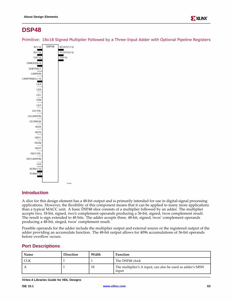
About Design Elements
DSP48
Primitive: 18x18 Signed Multiplier Followed by a Three-Input Adder with Optional Pipeline Registers
Intr oduction
A slice for this design element has a 48-bit output and is primarily intended for use in digital-signal processingapplications. However, the flexibility of this component means that it can be applied to many more applicationsthan a typical MACC unit. A basic DSP48 slice consists of a multiplier followed by an adder. The multiplieraccepts two, 18-bit, signed, two’s complement operands producing a 36-bit, signed, twos complement result.The result is sign extended to 48 bits. The adder accepts three, 48-bit, signed, twos’ complement operandsproducing a 48-bit, singed, twos’ complement result.
Possible operands for the adder include the multiplier output and external source or the registered output of theadder providing an accumulate function. The 48-bit output allows for 4096 accumulations of 36-bit operandsbefore overflow occurs.
Por t Descriptions
Name Direction Width Function
CLK I 1 The DSP48 clock
A I 18 The multiplier’s A input, can also be used as adder’s MSWinput
Vir tex-4 Libraries Guide for HDL Designs
ISE 10.1 www.xilinx.com 63
About Design Elements
Name Direction Width Function
B I 18 The multiplier’s B input, can also be used as adder’s LSWinput
BCIN I 18 The multiplier’s cascaded B input, can also be used as adder’sLSW input
C I 48 The adder’s C input
PCIN I 48 Cascaded adder’s C Input from previous DSP slice
CARRYIN I 1 The adders carry input
SUBTRACT I 1 0= add, 1= (C, PCIN)-(mult,A:B)
OPMODE I 7 Controls input to adder in DSP48 slices- see OPMODE table
CARRYINSEL I 2 Selects carry source - see CARRINSEL table
CEA I 1 Clock enable - 0=hold 1=enable AREG
CEB I 1 Clock enable - 0=hold 1=enable BREG
CEC I 1 Clock enable - 0=hold 1=enable CREG
CEP I 1 Clock enable - 0=hold 1=enable PREG
Synthesis Attributes Used to Define Pipeline Registers
The following table describes the synthesis attributes used to define the pipeline registers.
Attribute Function
AREG 0=bypass, 1=single, 2=dual
BREG 0=bypass, 1=single, 2=dual
CREG 0=bypass, 1=single
PREG 0=bypass, 1=single
MREG 0=bypass, 1=single
SUBTRACTREG 0=bypass, 1=single
OPMODEREG 0=bypass, 1=single
CARRYINSELREG 0=bypass, 1=single
Twos Complement Signed Multiplier
The multiplier inside the DSP48 slice is an 18-bit x 18-bit twos complement multiplier with a 36-bit signed twoscomplement result. Cascading of multipliers to achieve larger products is supported. Applications such assigned-signed, signed-unsigned, and unsigned-unsigned multiplication, logical, arithmetic, barrel-shifter, twoscomplement and magnitude return are easily implemented. There are two independent dynamic data inputports. The input ports can represent 18-bit signed or 17-bit unsigned data.
X, Y, and Z Multiplexers
The Operational Mode (OpMode) inputs provide a way for the design to change its functionality on the fly. Forexample, the loading of an accumulator to restart an accumulation process. The OpMode bits can be optionallyregistered under the control of the configuration RAM.
The following tables list the possible values of OpMode and resulting function at the outputs of the threemultiplexers supplying data to the adder/subtracter. The 7-bit OpMode control can be further broken down intomultiplexer select bits. Not all possible combinations for the multiplexer select bits are allowed. If the multiplieroutput is selected then both the X and Y multiplexer are consumed with the multiplier output.
OpMode Control Bit Select X, Y, and Z Multiplexer Outputs
Vir tex-4 Libraries Guide for HDL Designs
64 www.xilinx.com ISE 10.1
About Design Elements
OPMODE Binary X Multiplexer Output Fed to Add/Subtract
Z Y X
XXX XX 0 ZERO (Default)
XXX 1 1 Multiplier Output
XXX XX 10 P
XXX XX 11 A concatenated B
OpMode Control Bit Select X, Y, and Z Multiplexer Outputs
OPMODE Binary Y Multiplexer Output Fed to Add/Subtract
Z Y X
XXX 0 XX ZERO (Default)
XXX 1 1 Multiplier Output
XXX 10 XX Illegal selection
XXX 11 XX C
OpMode Controls X, Y, and Z Multiplexer Outputs
OPMODE Binary Y Multiplexer Output Fed to Add/Subtract
Z Y X
XXX 0 XX ZERO (Default)
XXX 1 1 Multiplier Output
XXX 10 XX Illegal selection
XXX 11 XX C
Three Input Adder/Subtracter Control Logic
The adder/subtracter output is a function of control and data inputs. The OpMode, as shown in the previoussection, selects the inputs to the X, Y, Z multiplexer that are directed to the three adder/subtracter inputs. It alsodescribed that when the multiplier output is selected, both X and Y multiplexers are occupied. With the inputs tothe adder/subtracter specified the function of the adder/subtracter itself must be examined. As with the inputmultiplexers, the OpMode bits specify a portion of this function. The table below shows this function. Thesymbol ± in the table means either add or subtract and is specified by the state of the subtract control.
Hex OpMode Binary OpMode Output of Adder/Subtracter Operation Description
[6:0] Z Y X
0x00 000 00 00 ±CIN Zero
0x02 000 00 10 ±(P + CIN) Hold P
0x03 000 00 11 ±(A:B + CIN) A:B select
0x05 000 01 01 ± (A ×B+CIN) Multiply
0x0c 000 11 00 ± (C + CIN) C select
0x0e 000 11 10 ± (C + P + CIN) Feedback add
0x0f 000 11 11 ± (A:B +C +CIN) 36-bit adder
0x10 001 00 00 PCIN ± CIN P cascade select
0x12 001 00 10 PCIN ± (P + CIN) P cascade feedback add
0x13 001 00 11 PCIN ±(A:B+CIN) P cascade add
Vir tex-4 Libraries Guide for HDL Designs
ISE 10.1 www.xilinx.com 65
About Design Elements
Hex OpMode Binary OpMode Output of Adder/Subtracter Operation Description
[6:0] Z Y X
0x15 001 01 01 PCIN ±(A ×B+CIN) P cascade multiply add
0x1c 001 11 00 PCIN ±(C+CIN) P cascade add
0x1e 001 11 10 PCIN ±(C+P+ CIN) P cascade feedback add add
0x1c 001 11 11 PCIN ±(A:B+C + CIN) P cascade add add
0x20 010 00 00 P±CIN Hold P
0x22 010 00 10 P±(P +CIN) Double feedback add
0x23 010 00 11 P±(A:B +CIN) Feedback add
0x25 010 01 01 P±(A ×B+ CIN) Multiply-accumulate
0x2c 010 11 00 P±(C +CIN) Feedback add
0x2e 010 11 10 P±(C +P+CIN) Double feedback add
0x2f 010 11 11 P±(A:B +C+CIN) Feedback add add
0x30 011 00 00 C±CIN C Select
0x32 011 00 10 C±(P +CIN) Feedback add
0x33 011 00 11 C±(A:B + CIN) 36-bit adder
0x35 011 01 01 C±(A ×B+CIN) Multiply add
0x3c 011 11 00 C±(C + CIN) Double
0x3e 011 11 10 C ± (C +P +CIN) Double add feedback add
0x3f 011 11 11 C±(A:B + C+ CIN) Double add
0x50 101 00 00 Shift(PCIN)± CIN 17-bit shift P cascade select
0x52 101 00 10 Shift(PCIN)±(P +CIN) 17-bit shift P cascade feedback add
0x53 101 00 11 Shift(PCIN)±(A:B +CIN) 17-bit shift P cascade add
0x55 101 01 01 Shift(PCIN)± (A ×B+ CIN) 17-bit shift P cascade multiply add
0x5c 101 11 00 Shift(PCIN)±(C +CIN) 17-bit shift P cascade add
0x5e 101 11 10 Shift(PCIN)±(C +P+CIN) 17-bit shift P cascade feedback addadd
0x5c 101 11 11 Shift(PCIN) ±(A:B+C +CIN) 17-bit shift P cascade add add
0x60 110 00 00 Shift(P) ± CIN 17-bit shift feedback
0x62 110 00 10 Shift(P) ± (P + CIN) 17-bit shift feedback feedback add
0x63 110 00 11 Shift(P) ± (A:B + CIN) 17-bit shift feedback add
0x65 110 01 01 Shift(P) ± (A ×B+CIN) 17-bit shift feedback multiply add
0x6c 110 11 00 Shift(P) ± (C + CIN) 17-bit shift feedback add
0x6e 110 11 10 Shift(P) ± (C + P + CIN) 17-bit shift feedback feedback add add
0x6f 110 11 11 Shift(P) ± (A:B + C + CIN) 17-bit shift feedback add add
Rounding Modes Supported by Carry Logic
In addition to the OpMode inputs, the data inputs to the three input adder/subtracter, and the subtract controlbit, the adder/subtracter output is a result of the carry-input logic.
Vir tex-4 Libraries Guide for HDL Designs
66 www.xilinx.com ISE 10.1
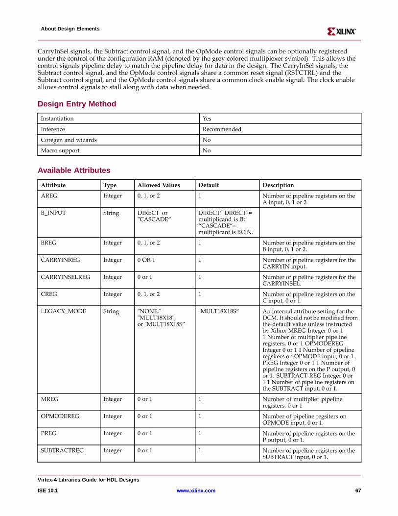
About Design Elements
CarryInSel signals, the Subtract control signal, and the OpMode control signals can be optionally registeredunder the control of the configuration RAM (denoted by the grey colored multiplexer symbol). This allows thecontrol signals pipeline delay to match the pipeline delay for data in the design. The CarryInSel signals, theSubtract control signal, and the OpMode control signals share a common reset signal (RSTCTRL) and theSubtract control signal, and the OpMode control signals share a common clock enable signal. The clock enableallows control signals to stall along with data when needed.
Design Entr y Method
Instantiation Yes
Inference Recommended
Coregen and wizards No
Macro support No
Availab le Attrib utes
Attribute Type Allowed Values Default Description
AREG Integer 0, 1, or 2 1 Number of pipeline registers on theA input, 0, 1 or 2
B_INPUT String DIRECT or"CASCADE”
DIRECT” DIRECT”=multiplicand is B;“CASCADE”=multiplicant is BCIN.
BREG Integer 0, 1, or 2 1 Number of pipeline registers on theB input, 0, 1 or 2.
CARRYINREG Integer 0 OR 1 1 Number of pipeline registers for theCARRYIN input.
CARRYINSELREG Integer 0 or 1 1 Number of pipeline registers for theCARRYINSEL.
CREG Integer 0, 1, or 2 1 Number of pipeline registers on theC input, 0 or 1.
LEGACY_MODE String "NONE,""MULT18X18",or "MULT18X18S”
"MULT18X18S” An internal attribute setting for theDCM. It should not be modified fromthe default value unless instructedby Xilinx MREG Integer 0 or 11 Number of multiplier pipelineregisters, 0 or 1 OPMODEREGInteger 0 or 1 1 Number of pipelineregsiters on OPMODE input, 0 or 1.PREG Integer 0 or 1 1 Number ofpipeline registers on the P output, 0or 1. SUBTRACT-REG Integer 0 or1 1 Number of pipeline registers onthe SUBTRACT input, 0 or 1.
MREG Integer 0 or 1 1 Number of multiplier pipelineregisters, 0 or 1
OPMODEREG Integer 0 or 1 1 Number of pipeline regsiters onOPMODE input, 0 or 1.
PREG Integer 0 or 1 1 Number of pipeline registers on theP output, 0 or 1.
SUBTRACTREG Integer 0 or 1 1 Number of pipeline registers on theSUBTRACT input, 0 or 1.
Vir tex-4 Libraries Guide for HDL Designs
ISE 10.1 www.xilinx.com 67
About Design Elements
VHDL Instantiation Template
Unless they already exist, copy the following two statements and paste them before the entity declaration.Library UNISIM;use UNISIM.vcomponents.all;
-- DSP48: DSP Function Block-- Virtex-4-- Xilinx HDL Libraries Guide, version 10.1.2
DSP48_inst : DSP48generic map (AREG=> 1, -- Number of pipeline registers on the A input, 0, 1 or 2BREG=> 1, -- Number of pipeline registers on the B input, 0, 1 or 2B_INPUT => "DIRECT", -- B input DIRECT from fabric or CASCADEfrom another DSP48CARRYINREG=> 1, -- Number of pipeline registers for the CARRYIN input, 0 or 1CARRYINSELREG=> 1, -- Number of pipeline registers for the CARRYINSEL, 0 or 1CREG=> 1, -- Number of pipeline registers on the C input, 0 or 1LEGACY_MODE=> "MULT18X18S", -- Backward compatibility, NONE, MULT18X18 or MULT18X18SMREG=> 1, -- Number of multiplier pipeline registers, 0 or 1OPMODEREG=> 1, -- Number of pipeline regsiters on OPMODEinput, 0 or 1PREG=> 1, -- Number of pipeline registers on the P output, 0 or 1SUBTRACTREG=> 1) -- Number of pipeline registers on the SUBTRACTinput, 0 or 1port map (BCOUT=> BCOUT, -- 18-bit B cascade outputP => P, -- 48-bit product outputPCOUT=> PCOUT, -- 48-bit cascade outputA => A, -- 18-bit A data inputB => B, -- 18-bit B data inputBCIN => BCIN, -- 18-bit B cascade inputC => C, -- 48-bit cascade inputCARRYIN => CARRYIN, -- Carry input signalCARRYINSEL => CARRYINSEL, -- 2-bit carry input selectCEA => CEA, -- A data clock enable inputCEB => CEB, -- B data clock enable inputCEC => CEC, -- C data clock enable inputCECARRYIN=> CECARRYIN, -- CARRYIN clock enable inputCECINSUB => CECINSUB, -- CINSUB clock enable inputCECTRL => CECTRL, -- Clock Enable input for CTRL regsitersLCEM=> CEM, -- Clock Enable input for multiplier regsitersCEP => CEP, -- Clock Enable input for P regsitersCLK => CLK, -- Clock inputOPMODE=> OPMODE,-- 7-bit operation mode inputPCIN => PCIN, -- 48-bit PCIN inputRSTA => RSTA, -- Reset input for A pipeline registersRSTB => RSTB, -- Reset input for B pipeline registersRSTC => RSTC, -- Reset input for C pipeline registersRSTCARRYIN=> RSTCARRYIN, -- Reset input for CARRYIN registersRSTCTRL => RSTCTRL, -- Reset input for CTRL registersRSTM=> RSTM, -- Reset input for multiplier registersRSTP => RSTP, -- Reset input for P pipeline registersSUBTRACT=> SUBTRACT-- SUBTRACTinput);
-- End of DSP48_inst instantiation
Verilog Instantiation Template
// DSP48: DSP Function Block// Virtex-4// Xilinx HDL Libraries Guide, version 10.1.2
DSP48 #(.AREG(1), // Number of pipeline registers on the A input, 0, 1 or 2.BREG(1), // Number of pipeline registers on the B input, 0, 1 or 2.B_INPUT("DIRECT"), // B input DIRECT from fabric or CASCADEfrom another DSP48.CARRYINREG(1), // Number of pipeline registers for the CARRYIN input, 0 or 1.CARRYINSELREG(1), // Number of pipeline registers for the CARRYINSEL, 0 or 1.CREG(1), // Number of pipeline registers on the C input, 0 or 1
Vir tex-4 Libraries Guide for HDL Designs
68 www.xilinx.com ISE 10.1
About Design Elements
.LEGACY_MODE("MULT18X18S"), // Backward compatibility, NONE, MULT18X18 or MULT18X18S
.MREG(1), // Number of multiplier pipeline registers, 0 or 1
.OPMODEREG(1), // Number of pipeline regsiters on OPMODEinput, 0 or 1
.PREG(1), // Number of pipeline registers on the P output, 0 or 1
.SUBTRACTREG(1) // Number of pipeline registers on the SUBTRACTinput, 0 or 1) DSP48_inst (.BCOUT(BCOUT), // 18-bit B cascade output.P(P), // 48-bit product output.PCOUT(PCOUT), // 48-bit cascade output.A(A), // 18-bit A data input.B(B), // 18-bit B data input.BCIN(BCIN), // 18-bit B cascade input.C(C), // 48-bit cascade input.CARRYIN(CARRYIN), // Carry input signal.CARRYINSEL(CARRYINSEL), // 2-bit carry input select.CEA(CEA), // A data clock enable input.CEB(CEB), // B data clock enable input.CEC(CEC), // C data clock enable input.CECARRYIN(CECARRYIN), // CARRYIN clock enable input.CECINSUB(CECINSUB), // CINSUB clock enable input.CECTRL(CECTRL), // Clock Enable input for CTRL regsiters.CEM(CEM), // Clock Enable input for multiplier regsiters.CEP(CEP), // Clock Enable input for P regsiters.CLK(CLK), // Clock input.OPMODE(OPMODE),// 7-bit operation mode input.PCIN(PCIN), // 48-bit PCIN input.RSTA(RSTA), // Reset input for A pipeline registers.RSTB(RSTB), // Reset input for B pipeline registers.RSTC(RSTC), // Reset input for C pipeline registers.RSTCARRYIN(RSTCARRYIN), // Reset input for CARRYIN registers.RSTCTRL(RSTCTRL), // Reset input for CTRL registers.RSTM(RSTM), // Reset input for multiplier registers.RSTP(RSTP), // Reset input for P pipeline registers.SUBTRACT(SUBTRACT) // SUBTRACTinput);
// End of DSP48_inst instantiation
For More Information
• See the Virtex-4 User Guide.
• See the Virtex-4 Data Sheets.
Vir tex-4 Libraries Guide for HDL Designs
ISE 10.1 www.xilinx.com 69
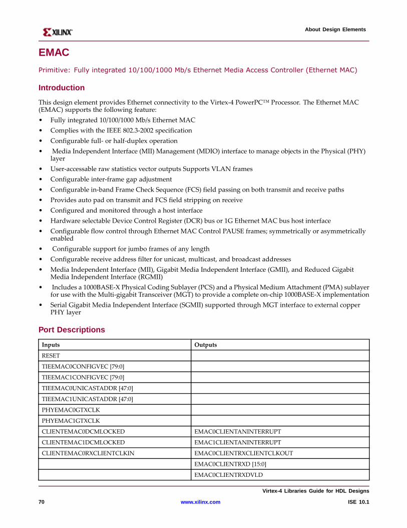
About Design Elements
EMAC
Primitive: Fully integrated 10/100/1000 Mb/s Ethernet Media Access Controller (Ethernet MAC)
Intr oduction
This design element provides Ethernet connectivity to the Virtex-4 PowerPC™ Processor. The Ethernet MAC(EMAC) supports the following feature:• Fully integrated 10/100/1000 Mb/s Ethernet MAC• Complies with the IEEE 802.3-2002 specification• Configurable full- or half-duplex operation• Media Independent Interface (MII) Management (MDIO) interface to manage objects in the Physical (PHY)
layer• User-accessable raw statistics vector outputs Supports VLAN frames• Configurable inter-frame gap adjustment• Configurable in-band Frame Check Sequence (FCS) field passing on both transmit and receive paths• Provides auto pad on transmit and FCS field stripping on receive• Configured and monitored through a host interface• Hardware selectable Device Control Register (DCR) bus or 1G Ethernet MAC bus host interface• Configurable flow control through Ethernet MAC Control PAUSE frames; symmetrically or asymmetrically
enabled• Configurable support for jumbo frames of any length• Configurable receive address filter for unicast, multicast, and broadcast addresses• Media Independent Interface (MII), Gigabit Media Independent Interface (GMII), and Reduced Gigabit
Media Independent Interface (RGMII)• Includes a 1000BASE-X Physical Coding Sublayer (PCS) and a Physical Medium Attachment (PMA) sublayer
for use with the Multi-gigabit Transceiver (MGT) to provide a complete on-chip 1000BASE-X implementation• Serial Gigabit Media Independent Interface (SGMII) supported through MGT interface to external copper
PHY layer
Por t Descriptions
Inputs Outputs
RESET
TIEEMAC0CONFIGVEC [79:0]
TIEEMAC1CONFIGVEC [79:0]
TIEEMAC0UNICASTADDR [47:0]
TIEEMAC1UNICASTADDR [47:0]
PHYEMAC0GTXCLK
PHYEMAC1GTXCLK
CLIENTEMAC0DCMLOCKED EMAC0CLIENTANINTERRUPT
CLIENTEMAC1DCMLOCKED EMAC1CLIENTANINTERRUPT
CLIENTEMAC0RXCLIENTCLKIN EMAC0CLIENTRXCLIENTCLKOUT
EMAC0CLIENTRXD [15:0]
EMAC0CLIENTRXDVLD
Vir tex-4 Libraries Guide for HDL Designs
70 www.xilinx.com ISE 10.1
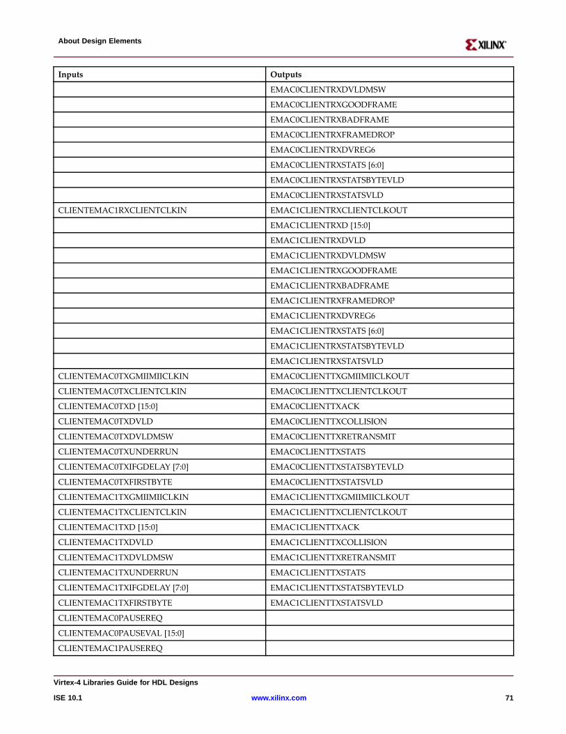
About Design Elements
Inputs Outputs
EMAC0CLIENTRXDVLDMSW
EMAC0CLIENTRXGOODFRAME
EMAC0CLIENTRXBADFRAME
EMAC0CLIENTRXFRAMEDROP
EMAC0CLIENTRXDVREG6
EMAC0CLIENTRXSTATS [6:0]
EMAC0CLIENTRXSTATSBYTEVLD
EMAC0CLIENTRXSTATSVLD
CLIENTEMAC1RXCLIENTCLKIN EMAC1CLIENTRXCLIENTCLKOUT
EMAC1CLIENTRXD [15:0]
EMAC1CLIENTRXDVLD
EMAC1CLIENTRXDVLDMSW
EMAC1CLIENTRXGOODFRAME
EMAC1CLIENTRXBADFRAME
EMAC1CLIENTRXFRAMEDROP
EMAC1CLIENTRXDVREG6
EMAC1CLIENTRXSTATS [6:0]
EMAC1CLIENTRXSTATSBYTEVLD
EMAC1CLIENTRXSTATSVLD
CLIENTEMAC0TXGMIIMIICLKIN EMAC0CLIENTTXGMIIMIICLKOUT
CLIENTEMAC0TXCLIENTCLKIN EMAC0CLIENTTXCLIENTCLKOUT
CLIENTEMAC0TXD [15:0] EMAC0CLIENTTXACK
CLIENTEMAC0TXDVLD EMAC0CLIENTTXCOLLISION
CLIENTEMAC0TXDVLDMSW EMAC0CLIENTTXRETRANSMIT
CLIENTEMAC0TXUNDERRUN EMAC0CLIENTTXSTATS
CLIENTEMAC0TXIFGDELAY [7:0] EMAC0CLIENTTXSTATSBYTEVLD
CLIENTEMAC0TXFIRSTBYTE EMAC0CLIENTTXSTATSVLD
CLIENTEMAC1TXGMIIMIICLKIN EMAC1CLIENTTXGMIIMIICLKOUT
CLIENTEMAC1TXCLIENTCLKIN EMAC1CLIENTTXCLIENTCLKOUT
CLIENTEMAC1TXD [15:0] EMAC1CLIENTTXACK
CLIENTEMAC1TXDVLD EMAC1CLIENTTXCOLLISION
CLIENTEMAC1TXDVLDMSW EMAC1CLIENTTXRETRANSMIT
CLIENTEMAC1TXUNDERRUN EMAC1CLIENTTXSTATS
CLIENTEMAC1TXIFGDELAY [7:0] EMAC1CLIENTTXSTATSBYTEVLD
CLIENTEMAC1TXFIRSTBYTE EMAC1CLIENTTXSTATSVLD
CLIENTEMAC0PAUSEREQ
CLIENTEMAC0PAUSEVAL [15:0]
CLIENTEMAC1PAUSEREQ
Vir tex-4 Libraries Guide for HDL Designs
ISE 10.1 www.xilinx.com 71
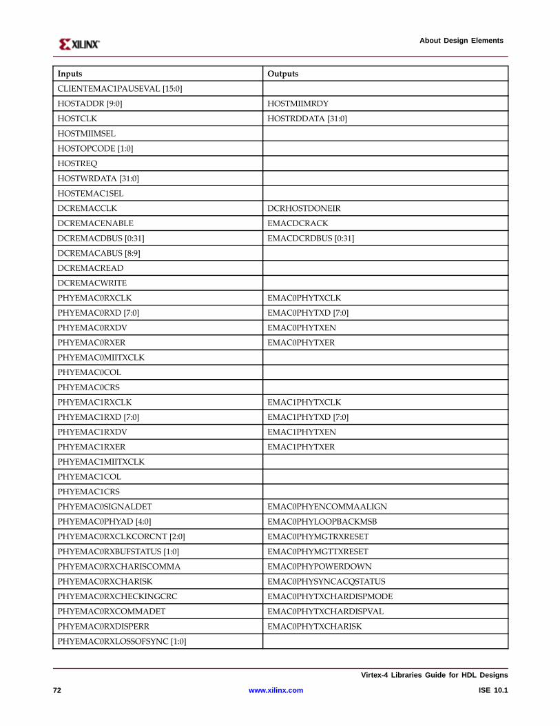
About Design Elements
Inputs Outputs
CLIENTEMAC1PAUSEVAL [15:0]
HOSTADDR [9:0] HOSTMIIMRDY
HOSTCLK HOSTRDDATA [31:0]
HOSTMIIMSEL
HOSTOPCODE [1:0]
HOSTREQ
HOSTWRDATA [31:0]
HOSTEMAC1SEL
DCREMACCLK DCRHOSTDONEIR
DCREMACENABLE EMACDCRACK
DCREMACDBUS [0:31] EMACDCRDBUS [0:31]
DCREMACABUS [8:9]
DCREMACREAD
DCREMACWRITE
PHYEMAC0RXCLK EMAC0PHYTXCLK
PHYEMAC0RXD [7:0] EMAC0PHYTXD [7:0]
PHYEMAC0RXDV EMAC0PHYTXEN
PHYEMAC0RXER EMAC0PHYTXER
PHYEMAC0MIITXCLK
PHYEMAC0COL
PHYEMAC0CRS
PHYEMAC1RXCLK EMAC1PHYTXCLK
PHYEMAC1RXD [7:0] EMAC1PHYTXD [7:0]
PHYEMAC1RXDV EMAC1PHYTXEN
PHYEMAC1RXER EMAC1PHYTXER
PHYEMAC1MIITXCLK
PHYEMAC1COL
PHYEMAC1CRS
PHYEMAC0SIGNALDET EMAC0PHYENCOMMAALIGN
PHYEMAC0PHYAD [4:0] EMAC0PHYLOOPBACKMSB
PHYEMAC0RXCLKCORCNT [2:0] EMAC0PHYMGTRXRESET
PHYEMAC0RXBUFSTATUS [1:0] EMAC0PHYMGTTXRESET
PHYEMAC0RXCHARISCOMMA EMAC0PHYPOWERDOWN
PHYEMAC0RXCHARISK EMAC0PHYSYNCACQSTATUS
PHYEMAC0RXCHECKINGCRC EMAC0PHYTXCHARDISPMODE
PHYEMAC0RXCOMMADET EMAC0PHYTXCHARDISPVAL
PHYEMAC0RXDISPERR EMAC0PHYTXCHARISK
PHYEMAC0RXLOSSOFSYNC [1:0]
Vir tex-4 Libraries Guide for HDL Designs
72 www.xilinx.com ISE 10.1
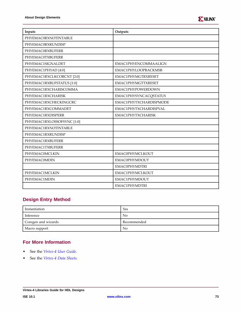
About Design Elements
Inputs Outputs
PHYEMAC0RXNOTINTABLE
PHYEMAC0RXRUNDISP
PHYEMAC0RXBUFERR
PHYEMAC0TXBUFERR
PHYEMAC1SIGNALDET EMAC1PHYENCOMMAALIGN
PHYEMAC1PHYAD [4:0] EMAC1PHYLOOPBACKMSB
PHYEMAC1RXCLKCORCNT [2:0] EMAC1PHYMGTRXRESET
PHYEMAC1RXBUFSTATUS [1:0] EMAC1PHYMGTTXRESET
PHYEMAC1RXCHARISCOMMA EMAC1PHYPOWERDOWN
PHYEMAC1RXCHARISK EMAC1PHYSYNCACQSTATUS
PHYEMAC1RXCHECKINGCRC EMAC1PHYTXCHARDISPMODE
PHYEMAC1RXCOMMADET EMAC1PHYTXCHARDISPVAL
PHYEMAC1RXDISPERR EMAC1PHYTXCHARISK
PHYEMAC1RXLOSSOFSYNC [1:0]
PHYEMAC1RXNOTINTABLE
PHYEMAC1RXRUNDISP
PHYEMAC1RXBUFERR
PHYEMAC1TXBUFERR
PHYEMAC0MCLKIN EMAC0PHYMCLKOUT
PHYEMAC0MDIN EMAC0PHYMDOUT
EMAC0PHYMDTRI
PHYEMAC1MCLKIN EMAC1PHYMCLKOUT
PHYEMAC1MDIN EMAC1PHYMDOUT
EMAC1PHYMDTRI
Design Entr y Method
Instantiation Yes
Inference No
Coregen and wizards Recommended
Macro support No
For More Information
• See the Virtex-4 User Guide.
• See the Virtex-4 Data Sheets.
Vir tex-4 Libraries Guide for HDL Designs
ISE 10.1 www.xilinx.com 73
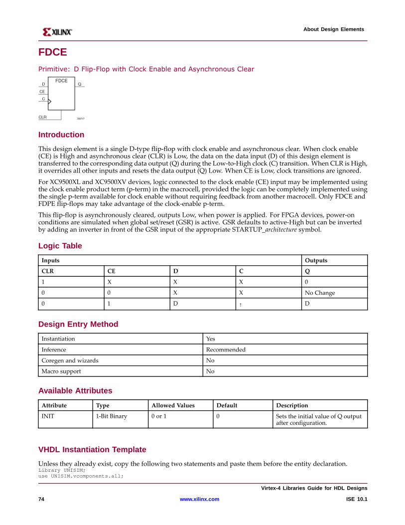
About Design Elements
FDCE
Primitive: D Flip-Flop with Clock Enable and Asynchronous Clear
Intr oduction
This design element is a single D-type flip-flop with clock enable and asynchronous clear. When clock enable(CE) is High and asynchronous clear (CLR) is Low, the data on the data input (D) of this design element istransferred to the corresponding data output (Q) during the Low-to-High clock (C) transition. When CLR is High,it overrides all other inputs and resets the data output (Q) Low. When CE is Low, clock transitions are ignored.
For XC9500XL and XC9500XV devices, logic connected to the clock enable (CE) input may be implemented usingthe clock enable product term (p-term) in the macrocell, provided the logic can be completely implemented usingthe single p-term available for clock enable without requiring feedback from another macrocell. Only FDCE andFDPE flip-flops may take advantage of the clock-enable p-term.
This flip-flop is asynchronously cleared, outputs Low, when power is applied. For FPGA devices, power-onconditions are simulated when global set/reset (GSR) is active. GSR defaults to active-High but can be invertedby adding an inverter in front of the GSR input of the appropriate STARTUP_architecture symbol.
Logic Table
Inputs Outputs
CLR CE D C Q
1 X X X 0
0 0 X X No Change
0 1 D ↑ D
Design Entr y Method
Instantiation Yes
Inference Recommended
Coregen and wizards No
Macro support No
Availab le Attrib utes
Attribute Type Allowed Values Default Description
INIT 1-Bit Binary 0 or 1 0 Sets the initial value of Q outputafter configuration.
VHDL Instantiation Template
Unless they already exist, copy the following two statements and paste them before the entity declaration.Library UNISIM;use UNISIM.vcomponents.all;
Vir tex-4 Libraries Guide for HDL Designs
74 www.xilinx.com ISE 10.1
About Design Elements
-- FDCE: Single Data Rate D Flip-Flop with Asynchronous Clear and-- Clock Enable (posedge clk). All families.-- Xilinx HDL Libraries Guide, version 10.1.2
FDCE_inst : FDCEgeneric map (INIT => ’0’) -- Initial value of register (’0’ or ’1’)port map (Q => Q, -- Data outputC => C, -- Clock inputCE => CE, -- Clock enable inputCLR => CLR, -- Asynchronous clear inputD => D -- Data input);
-- End of FDCE_inst instantiation
Verilog Instantiation Template
// FDCE: Single Data Rate D Flip-Flop with Asynchronous Clear and// Clock Enable (posedge clk).// All families.// Xilinx HDL Libraries Guide, version 10.1.2
FDCE #(.INIT(1’b0) // Initial value of register (1’b0 or 1’b1)) FDCE_inst (.Q(Q), // Data output.C(C), // Clock input.CE(CE), // Clock enable input.CLR(CLR), // Asynchronous clear input.D(D) // Data input);
// End of FDCE_inst instantiation
For More Information
• See the Virtex-4 User Guide.
• See the Virtex-4 Data Sheets.
Vir tex-4 Libraries Guide for HDL Designs
ISE 10.1 www.xilinx.com 75
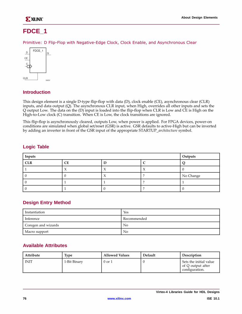
About Design Elements
FDCE_1
Primitive: D Flip-Flop with Negative-Edge Clock, Clock Enable, and Asynchronous Clear
Intr oduction
This design element is a single D-type flip-flop with data (D), clock enable (CE), asynchronous clear (CLR)inputs, and data output (Q). The asynchronous CLR input, when High, overrides all other inputs and sets theQ output Low. The data on the (D) input is loaded into the flip-flop when CLR is Low and CE is High on theHigh-to-Low clock (C) transition. When CE is Low, the clock transitions are ignored.
This flip-flop is asynchronously cleared, outputs Low, when power is applied. For FPGA devices, power-onconditions are simulated when global set/reset (GSR) is active. GSR defaults to active-High but can be invertedby adding an inverter in front of the GSR input of the appropriate STARTUP_architecture symbol.
Logic Table
Inputs Outputs
CLR CE D C Q
1 X X X 0
0 0 X ? No Change
0 1 1 ? 1
0 1 0 ? 0
Design Entr y Method
Instantiation Yes
Inference Recommended
Coregen and wizards No
Macro support No
Availab le Attrib utes
Attribute Type Allowed Values Default Description
INIT 1-Bit Binary 0 or 1 0 Sets the initial valueof Q output afterconfiguration.
Vir tex-4 Libraries Guide for HDL Designs
76 www.xilinx.com ISE 10.1
About Design Elements
VHDL Instantiation Template
Unless they already exist, copy the following two statements and paste them before the entity declaration.Library UNISIM;use UNISIM.vcomponents.all;
-- FDCE_1: Single Data Rate D Flip-Flop with Asynchronous Clear and-- Clock Enable (negedge clock). All families.-- Xilinx HDL Libraries Guide, version 10.1.2
FDCE_1_inst : FDCE_1generic map (INIT => ’0’) -- Initial value of register (’0’ or ’1’)port map (Q => Q, -- Data outputC => C, -- Clock inputCE => CE, -- Clock enable inputCLR => CLR, -- Asynchronous clear inputD => D -- Data input);
-- End of FDCE_1_inst instantiation
Verilog Instantiation Template
// FDCE_1: Single Data Rate D Flip-Flop with Asynchronous Clear and// Clock Enable (negedge clock).// All families.// Xilinx HDL Libraries Guide, version 10.1.2
FDCE_1 #(.INIT(1’b0) // Initial value of register (1’b0 or 1’b1)) FDCE_1_inst (.Q(Q), // Data output.C(C), // Clock input.CE(CE), // Clock enable input.CLR(CLR), // Asynchronous clear input.D(D) // Data input);
// End of FDCE_1_inst instantiation
For More Information
• See the Virtex-4 User Guide.
• See the Virtex-4 Data Sheets.
Vir tex-4 Libraries Guide for HDL Designs
ISE 10.1 www.xilinx.com 77

About Design Elements
FDCPE
Primitive: D Flip-Flop with Clock Enable and Asynchronous Preset and Clear
Intr oduction
This design element is a single D-type flip-flop with data (D), clock enable (CE), asynchronous preset (PRE),and asynchronous clear (CLR) inputs. The asynchronous active high PRE sets the Q output High; that activehigh CLR resets the output Low and has precedence over the PRE input. Data on the D input is loaded into theflip-flop when PRE and CLR are Low and CE is High on the Low-to-High clock (C) transition. When CE is Low,the clock transitions are ignored and the previous value is retained. The FDCPE is generally implemented as aslice or IOB register within the device.
For FPGA devices, upon power-up, the initial value of this component is specified by the INIT attribute. If asubsequent GSR (Global Set/Reset) is asserted, the flop is asynchronously set to the INIT value.
Note While this device supports the use of asynchronous set and reset, it is not generally recommended tobe used for in most cases. Use of asynchronous signals pose timing issues within the design that are difficultto detect and control and also have an adverse affect on logic optimization causing a larger design that canconsume more power than if a synchronous set or reset is used.
Logic Table
Inputs Outputs
CLR PRE CE D C Q
1 X X X X 0
0 1 X X X 1
0 0 0 X X No Change
0 0 1 D ↑ D
Por t Descriptions
Name Direction Width Function
Q Output 1-Bit Data output
C Input 1-Bit Clock input
CE Input 1-Bit Clock enable input
CLR Input 1-Bit Asynchronous clear input
D Input 1-Bit Data input
PRE Input 1-Bit Asynchronous set input
Vir tex-4 Libraries Guide for HDL Designs
78 www.xilinx.com ISE 10.1
About Design Elements
Design Entr y Method
Instantiation Yes
Inference Recommended
Coregen and wizards No
Macro support No
Availab le Attrib utes
Attribute Type Allowed Values Default Description
INIT 1-Bit Binary 0 or 1 0 Sets the initial value of Q output afterconfiguration and on GSR.
VHDL Instantiation Template
Unless they already exist, copy the following two statements and paste them before the entity declaration.Library UNISIM;use UNISIM.vcomponents.all;
-- FDCPE: Single Data Rate D Flip-Flop with Asynchronous Clear, Set and-- Clock Enable (posedge clk). All families.-- Xilinx HDL Libraries Guide, version 10.1.2
FDCPE_inst : FDCPEgeneric map (INIT => ’0’) -- Initial value of register (’0’ or ’1’)port map (Q => Q, -- Data outputC => C, -- Clock inputCE => CE, -- Clock enable inputCLR => CLR, -- Asynchronous clear inputD => D, -- Data inputPRE => PRE -- Asynchronous set input);
-- End of FDCPE_inst instantiation
Vir tex-4 Libraries Guide for HDL Designs
ISE 10.1 www.xilinx.com 79
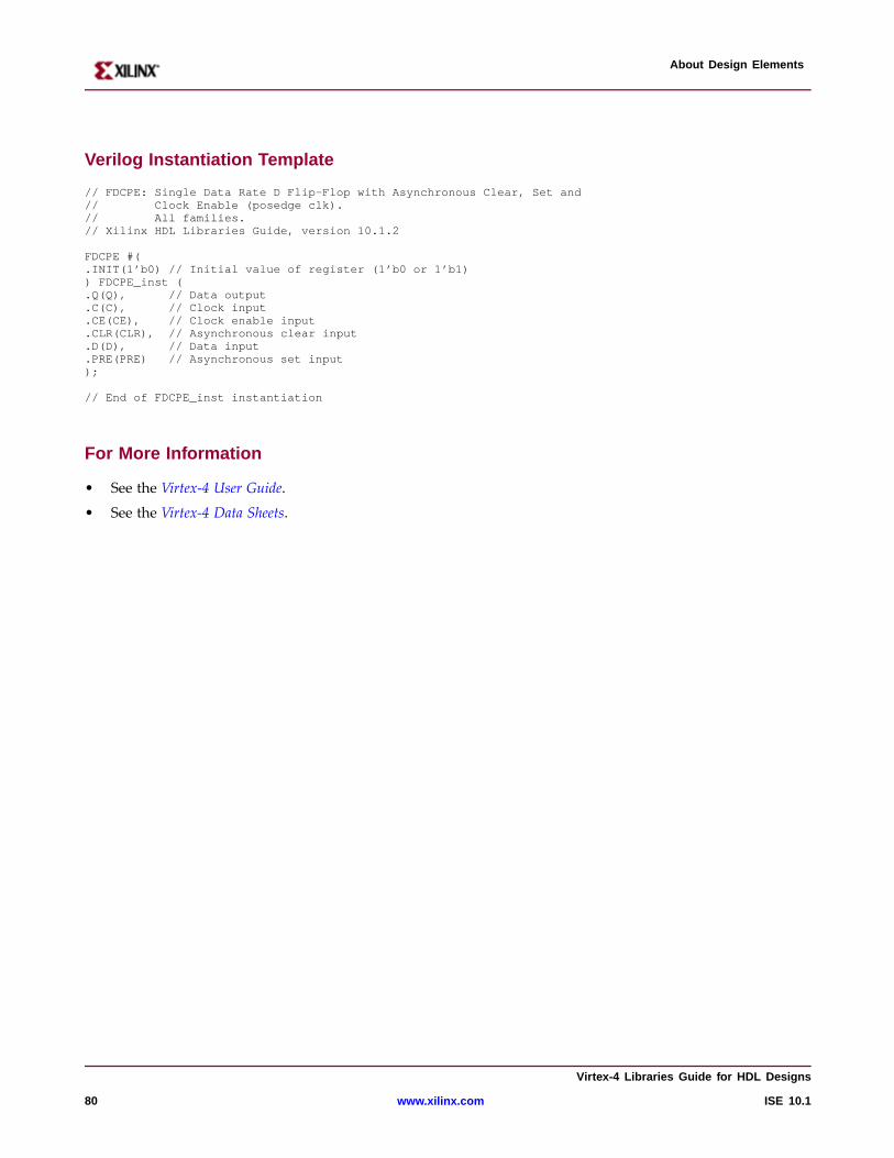
About Design Elements
Verilog Instantiation Template
// FDCPE: Single Data Rate D Flip-Flop with Asynchronous Clear, Set and// Clock Enable (posedge clk).// All families.// Xilinx HDL Libraries Guide, version 10.1.2
FDCPE #(.INIT(1’b0) // Initial value of register (1’b0 or 1’b1)) FDCPE_inst (.Q(Q), // Data output.C(C), // Clock input.CE(CE), // Clock enable input.CLR(CLR), // Asynchronous clear input.D(D), // Data input.PRE(PRE) // Asynchronous set input);
// End of FDCPE_inst instantiation
For More Information
• See the Virtex-4 User Guide.
• See the Virtex-4 Data Sheets.
Vir tex-4 Libraries Guide for HDL Designs
80 www.xilinx.com ISE 10.1
About Design Elements
FDCPE_1
Primitive: D Flip-Flop with Negative-Edge Clock, Clock Enable, and Asynchronous Preset and Clear
Intr oduction
FDCPE_1 is a single D-type flip-flop with data (D), clock enable (CE), asynchronous preset (PRE), andasynchronous clear (CLR) inputs and data output (Q). The asynchronous PRE, when High, sets the (Q) outputHigh; CLR, when High, resets the output Low. Data on the (D) input is loaded into the flip-flop when PRE andCLR are Low and CE is High on the High-to-Low clock (C) transition. When CE is Low, the clock transitionsare ignored.
This flip-flop is asynchronously cleared, outputs Low, when power is applied. For FPGA devices, power-onconditions are simulated when global set/reset (GSR) is active. GSR defaults to active-High but can be invertedby adding an inverter in front of the GSR input of the appropriate STARTUP_architecture symbol.
Logic Table
Inputs Outputs
CLR PRE CE D C Q
1 X X X X 0
0 1 X X X 1
0 0 0 X X No Change
0 0 1 D ↓ D
Por t Descriptions
Name Direction Width Function
Q Output 1-Bit Data output
C Input 1-Bit Clock input
CE Input 1-Bit Clock enable input
CLR Input 1-Bit Asynchronous clear input
D Input 1-Bit Data input
PRE Input 1-Bit Asynchronous set input
Design Entr y Method
Instantiation Yes
Inference Recommended
Vir tex-4 Libraries Guide for HDL Designs
ISE 10.1 www.xilinx.com 81
About Design Elements
Coregen and wizards No
Macro support No
Availab le Attrib utes
Attribute Type Allowed Values Default Description
INIT 1-Bit Binary 0 or 1 0 Sets the initial valueof Q output afterconfiguration
VHDL Instantiation Template
Unless they already exist, copy the following two statements and paste them before the entity declaration.Library UNISIM;use UNISIM.vcomponents.all;
-- FDCPE_1: Single Data Rate D Flip-Flop with Asynchronous Clear, Set and-- Clock Enable (negedge clock). All families.-- Xilinx HDL Libraries Guide, version 10.1.2
FDCPE_1_inst : FDCPE_1generic map (INIT => ’0’) -- Initial value of register (’0’ or ’1’)port map (Q => Q, -- Data outputC => C, -- Clock inputCE => CE, -- Clock enable inputCLR => CLR, -- Asynchronous clear inputD => D, -- Data inputPRE => PRE -- Asynchronous set input);
-- End of FDCPE_1_inst instantiation
Verilog Instantiation Template
// FDCPE_1: Single Data Rate D Flip-Flop with Asynchronous Clear, Set and// Clock Enable (negedge clock).// All families.// Xilinx HDL Libraries Guide, version 10.1.2
FDCPE_1 #(.INIT(1’b0) // Initial value of register (1’b0 or 1’b1)) FDCPE_1_inst (.Q(Q), // Data output.C(C), // Clock input.CE(CE), // Clock enable input.CLR(CLR), // Asynchronous clear input.D(D), // Data input.PRE(PRE) // Asynchronous set input);
// End of FDCPE_1_inst instantiation
For More Information
• See the Virtex-4 User Guide.• See the Virtex-4 Data Sheets.
Vir tex-4 Libraries Guide for HDL Designs
82 www.xilinx.com ISE 10.1
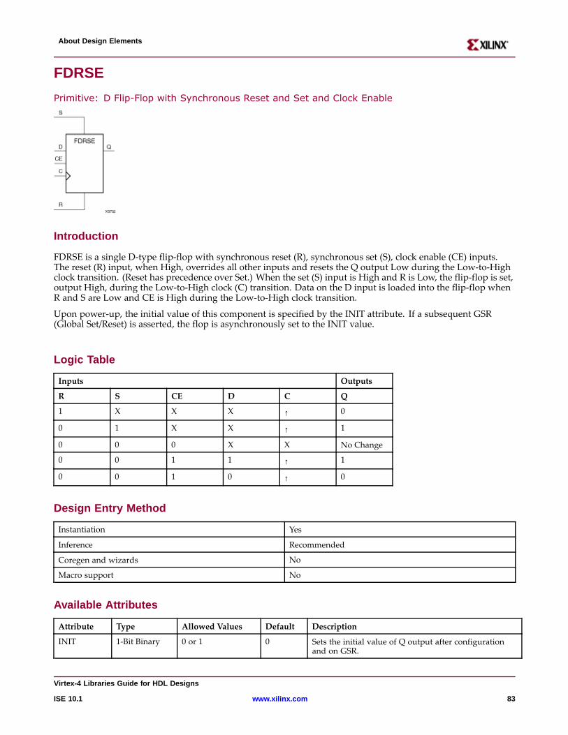
About Design Elements
FDRSE
Primitive: D Flip-Flop with Synchronous Reset and Set and Clock Enable
Intr oduction
FDRSE is a single D-type flip-flop with synchronous reset (R), synchronous set (S), clock enable (CE) inputs.The reset (R) input, when High, overrides all other inputs and resets the Q output Low during the Low-to-Highclock transition. (Reset has precedence over Set.) When the set (S) input is High and R is Low, the flip-flop is set,output High, during the Low-to-High clock (C) transition. Data on the D input is loaded into the flip-flop whenR and S are Low and CE is High during the Low-to-High clock transition.
Upon power-up, the initial value of this component is specified by the INIT attribute. If a subsequent GSR(Global Set/Reset) is asserted, the flop is asynchronously set to the INIT value.
Logic Table
Inputs Outputs
R S CE D C Q
1 X X X ↑ 0
0 1 X X ↑ 1
0 0 0 X X No Change
0 0 1 1 ↑ 1
0 0 1 0 ↑ 0
Design Entr y Method
Instantiation Yes
Inference Recommended
Coregen and wizards No
Macro support No
Availab le Attrib utes
Attribute Type Allowed Values Default Description
INIT 1-Bit Binary 0 or 1 0 Sets the initial value of Q output after configurationand on GSR.
Vir tex-4 Libraries Guide for HDL Designs
ISE 10.1 www.xilinx.com 83
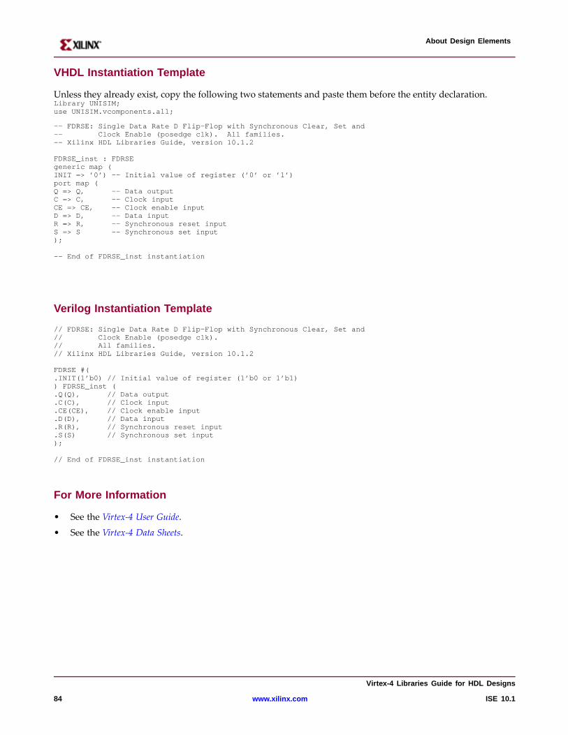
About Design Elements
VHDL Instantiation Template
Unless they already exist, copy the following two statements and paste them before the entity declaration.Library UNISIM;use UNISIM.vcomponents.all;
-- FDRSE: Single Data Rate D Flip-Flop with Synchronous Clear, Set and-- Clock Enable (posedge clk). All families.-- Xilinx HDL Libraries Guide, version 10.1.2
FDRSE_inst : FDRSEgeneric map (INIT => ’0’) -- Initial value of register (’0’ or ’1’)port map (Q => Q, -- Data outputC => C, -- Clock inputCE => CE, -- Clock enable inputD => D, -- Data inputR => R, -- Synchronous reset inputS => S -- Synchronous set input);
-- End of FDRSE_inst instantiation
Verilog Instantiation Template
// FDRSE: Single Data Rate D Flip-Flop with Synchronous Clear, Set and// Clock Enable (posedge clk).// All families.// Xilinx HDL Libraries Guide, version 10.1.2
FDRSE #(.INIT(1’b0) // Initial value of register (1’b0 or 1’b1)) FDRSE_inst (.Q(Q), // Data output.C(C), // Clock input.CE(CE), // Clock enable input.D(D), // Data input.R(R), // Synchronous reset input.S(S) // Synchronous set input);
// End of FDRSE_inst instantiation
For More Information
• See the Virtex-4 User Guide.
• See the Virtex-4 Data Sheets.
Vir tex-4 Libraries Guide for HDL Designs
84 www.xilinx.com ISE 10.1
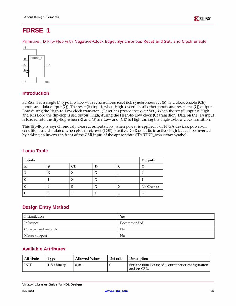
About Design Elements
FDRSE_1
Primitive: D Flip-Flop with Negative-Clock Edge, Synchronous Reset and Set, and Clock Enable
Intr oduction
FDRSE_1 is a single D-type flip-flop with synchronous reset (R), synchronous set (S), and clock enable (CE)inputs and data output (Q). The reset (R) input, when High, overrides all other inputs and resets the (Q) outputLow during the High-to-Low clock transition. (Reset has precedence over Set.) When the set (S) input is Highand R is Low, the flip-flop is set, output High, during the High-to-Low clock (C) transition. Data on the (D) inputis loaded into the flip-flop when (R) and (S) are Low and (CE) is High during the High-to-Low clock transition.
This flip-flop is asynchronously cleared, outputs Low, when power is applied. For FPGA devices, power-onconditions are simulated when global set/reset (GSR) is active. GSR defaults to active-High but can be invertedby adding an inverter in front of the GSR input of the appropriate STARTUP_architecture symbol.
Logic Table
Inputs Outputs
R S CE D C Q
1 X X X ↓ 0
0 1 X X ↓ 1
0 0 0 X X No Change
0 0 1 D ↓ D
Design Entr y Method
Instantiation Yes
Inference Recommended
Coregen and wizards No
Macro support No
Availab le Attrib utes
Attribute Type Allowed Values Default Description
INIT 1-Bit Binary 0 or 1 0 Sets the initial value of Q output after configurationand on GSR.
Vir tex-4 Libraries Guide for HDL Designs
ISE 10.1 www.xilinx.com 85
About Design Elements
VHDL Instantiation Template
Unless they already exist, copy the following two statements and paste them before the entity declaration.Library UNISIM;use UNISIM.vcomponents.all;
-- FDRSE_1: Single Data Rate D Flip-Flop with Synchronous Clear, Set and-- Clock Enable (negedge clock). All families.-- Xilinx HDL Libraries Guide, version 10.1.2
FDRSE_1_inst : FDRSE_1generic map (INIT => ’0’) -- Initial value of register (’0’ or ’1’)port map (Q => Q, -- Data outputC => C, -- Clock inputCE => CE, -- Clock enable inputD => D, -- Data inputR => R, -- Synchronous reset inputS => S -- Synchronous set input);
-- End of FDRSE_1_inst instantiation
Verilog Instantiation Template
// FDRSE_1: Single Data Rate D Flip-Flop with Synchronous Clear, Set and// Clock Enable (negedge clock).// All families.// Xilinx HDL Libraries Guide, version 10.1.2
FDRSE_1 #(.INIT(1’b0) // Initial value of register (1’b0 or 1’b1)) FDRSE_1_inst (.Q(Q), // Data output.C(C), // Clock input.CE(CE), // Clock enable input.D(D), // Data input.R(R), // Synchronous reset input.S(S) // Synchronous set input);// End of FDRSE_1_inst instantiation
For More Information
• See the Virtex-4 User Guide.
• See the Virtex-4 Data Sheets.
Vir tex-4 Libraries Guide for HDL Designs
86 www.xilinx.com ISE 10.1
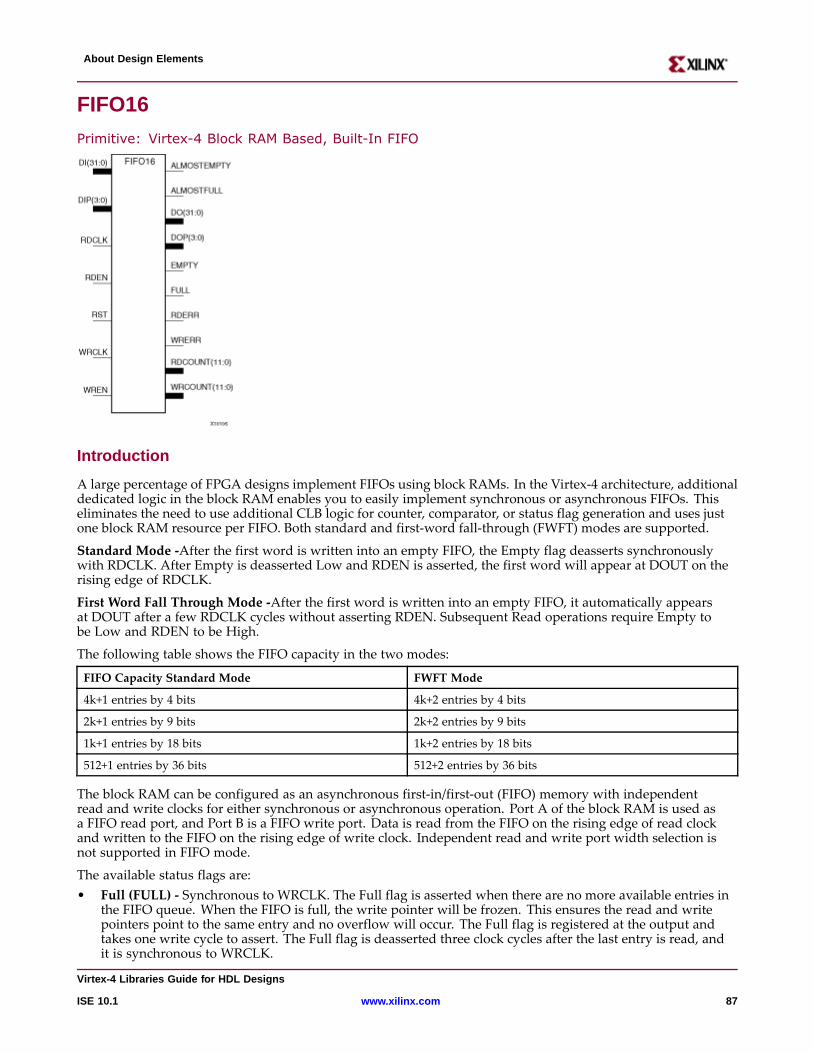
About Design Elements
FIFO16
Primitive: Virtex-4 Block RAM Based, Built-In FIFO
Intr oduction
A large percentage of FPGA designs implement FIFOs using block RAMs. In the Virtex-4 architecture, additionaldedicated logic in the block RAM enables you to easily implement synchronous or asynchronous FIFOs. Thiseliminates the need to use additional CLB logic for counter, comparator, or status flag generation and uses justone block RAM resource per FIFO. Both standard and first-word fall-through (FWFT) modes are supported.
Standard Mode -After the first word is written into an empty FIFO, the Empty flag deasserts synchronouslywith RDCLK. After Empty is deasserted Low and RDEN is asserted, the first word will appear at DOUT on therising edge of RDCLK.
First Word Fall Through Mode -After the first word is written into an empty FIFO, it automatically appearsat DOUT after a few RDCLK cycles without asserting RDEN. Subsequent Read operations require Empty tobe Low and RDEN to be High.
The following table shows the FIFO capacity in the two modes:
FIFO Capacity Standard Mode FWFT Mode
4k+1 entries by 4 bits 4k+2 entries by 4 bits
2k+1 entries by 9 bits 2k+2 entries by 9 bits
1k+1 entries by 18 bits 1k+2 entries by 18 bits
512+1 entries by 36 bits 512+2 entries by 36 bits
The block RAM can be configured as an asynchronous first-in/first-out (FIFO) memory with independentread and write clocks for either synchronous or asynchronous operation. Port A of the block RAM is used asa FIFO read port, and Port B is a FIFO write port. Data is read from the FIFO on the rising edge of read clockand written to the FIFO on the rising edge of write clock. Independent read and write port width selection isnot supported in FIFO mode.
The available status flags are:• Full (FULL) - Synchronous to WRCLK. The Full flag is asserted when there are no more available entries in
the FIFO queue. When the FIFO is full, the write pointer will be frozen. This ensures the read and writepointers point to the same entry and no overflow will occur. The Full flag is registered at the output andtakes one write cycle to assert. The Full flag is deasserted three clock cycles after the last entry is read, andit is synchronous to WRCLK.
Vir tex-4 Libraries Guide for HDL Designs
ISE 10.1 www.xilinx.com 87
About Design Elements
• Empty (EMPTY) - Synchronous to RDCLK.
• Almost Full (AFULL) - Synchronous to WRCLK. The Almost Full flag is set when the FIFO has fewer thanthe number of available empty spaces specified by the ALMOST_FULL_OFFSET value. The Almost Fullflag warns you to stop writing. It deasserts when the number of empty spaces in the FIFO is greater thanthe ALMOST_FULL_OFFSET value, and is synchronous to WRCLK.
• Almost Empty (AEMPTY) - Synchronous to RDCLK.
• Write Count (WRCOUNT) - Synchronous to WRCLK.
• Write Error (WRERR) - Synchronous to WRCLK. Once the Full flag has been asserted, any further writeattempts will trigger the Write Error flag. The Write Error flag is deasserted when Write Enable or Full isdeasserted Low. This signal is synchronous to WRCLK.
• Read Count (RDCOUNT) - Synchronous to RDCLK.
• Read Error (RDERR) - Synchronous to RDCLK.
Por t Descriptions
Name Direction Description
DI Input Data input
DIP Input Parity-bit input
WREN Input Write enable. WhenWREN = 1, data will be written to memory.When WREN = 0, write is disabled.
WRCLK Input Clock for write domain operation.
RDEN Input Read enable. When RDEN = 1, data will be read to outputregister. When RDEN = 0, read is disabled.
RDCLK Input Clock for read domain operation.
RESET Input Asynchronous reset of all FIFO functions, flags, and pointers.
DO Output Data output, synchronous to RDCLK
DOP Output Parity-bit output, synchronous to RDCLK
FULL Output All entries in FIFO memory are filled.
ALMOSTFULL Output Almost all entries in FIFO memory have been filled.Synchronous to WRCLK. The value is configurable by you.
EMPTY Output FIFO is empty. No additional read can be performed.Synchronous to RDCLK.
ALMOSTEMPTY Output Almost all valid entries in FIFO are read. Synchronous withRDCLK. The value is configurable by you.
RDCOUNT Output The FIFO data read pointer. It is synchronous with RDCLK.The value will wrap around if the maximum read pointer valuehas been reached.
WRCOUNT Output The FIFO data write pointer. It is synchronous with WRCLK.The value will wrap around if the maximum write pointervalue has been reached.
WRERR Output When the FIFO is full, any additional write operation generatesan error flag. Synchronous with WRCLK.
RDERR Output When the FIFO is empty, any additional read operationgenerates an error flag. Synchronous with RDCLK.
Vir tex-4 Libraries Guide for HDL Designs
88 www.xilinx.com ISE 10.1
About Design Elements
Design Entr y Method
Instantiation Recommended
Inference No
Coregen and wizards No
Macro support No
Availab le Attrib utes
Attribute Type Allowed Values Default Description
ALMOST_EMPTY_OFFSET
12-Bit Hexadecimal 12-Bit Hexadecimal 12’h080 Sets the almost emptythreshold.
ALMOST_FULL_OFFSET
12-Bit Hexadecimal 12-Bit Hexadecimal 12’h080 Sets almost fullthreshold.
DATA_WIDTH Integer 4, 9, 18, 36 36 Sets data width toallowed value.
FIRST_WORD_FALL_THROUGH
Boolean FALSE, TRUE FALSE Sets the FIFO FWFT to"TRUE" or "FALSE."
VHDL Instantiation Template
Unless they already exist, copy the following two statements and paste them before the entity declaration.Library UNISIM;use UNISIM.vcomponents.all;
-- FIFO16: Virtex-4 4k deep x 4 wide BlockRAM Asynchrnous FIFO-- Xilinx HDL Libraries Guide, version 10.1.2
FIFO16_inst : FIFO16generic map (ALMOST_FULL_OFFSET=> X"080", -- Sets almost full thresholdALMOST_EMPTY_OFFSET=> X"080", -- Sets the almost empty thresholdDATA_WIDTH=> 4, -- Sets data width to 4, 9, 18, or 36FIRST_WORD_FALL_THROUGH=> FALSE) --Sets the FIFO FWFT to TRUE or FALSEport map (ALMOSTEMPTY=> ALMOSTEMPTY,-- 1-bit almost empty output flagALMOSTFULL=> ALMOSTFULL, -- 1-bit almost full output flagDO (31 DOWNTO4) => unconnected (27 downto 0), -- Unused data output. Unconnected is a signal of 32 bitsDO (3 DOWNTO0) => DO, -- 4-bit data outputDOP => unconnected (31 downto 28), -- 4-bit Unused parity data output. Unconnected is a signal of 32 bitsEMPTY=> EMPTY, -- 1-bit empty output flagFULL => FULL, -- 1-bit full output flagRDCOUNT=> RDCOUNT, -- 12-bit read count outputRDERR=> RDERR, -- 1-bit read error outputWRCOUNT=> WRCOUNT, -- 12-bit write count outputWRERR=> WRERR, -- 1-bit write errorDI (31 DOWNTO4) => X"0000000", -- Unused data inputs tied to groundDI (3 downto 0) => DI, -- 4-bit data inputDIP => X"0", -- 4-bit Unused parity inputs tied to groundRDCLK => RDCLK, -- 1-bit read clock inputRDEN=> RDEN, -- 1-bit read enable inputRST => RST, -- 1-bit reset inputWRCLK=> WRCLK, -- 1-bit write clock inputWREN=> WREN -- 1-bit write enable input);
-- End of FIFO16_inst instantiation
Vir tex-4 Libraries Guide for HDL Designs
ISE 10.1 www.xilinx.com 89
About Design Elements
Verilog Instantiation Template
// FIFO16: Virtex-4 BlockRAM Asynchronous FIFO configured for 4k deep x 4 wide// Xilinx HDL Libraries Guide, version 10.1.2
wire [27:0] unconnected;
FIFO16 #(.ALMOST_FULL_OFFSET(12’h080), // Sets almost full threshold.ALMOST_EMPTY_OFFSET(12’h080), // Sets the almost empty threshold.DATA_WIDTH(4), // Sets data width to 4, 9, 18, or 36.FIRST_WORD_FALL_THROUGH("FALSE") // Sets the FIFO FWFT to "TRUE" or "FALSE") FIFO16_4kx4_inst (.ALMOSTEMPTY(ALMOSTEMPTY), // 1-bit almost empty output flag.ALMOSTFULL(ALMOSTFULL), // 1-bit almost full output flag.DO({unconnected[27:0], DO}), // 4-bit data output.EMPTY(EMPTY), // 1-bit empty output flag.FULL(FULL), // 1-bit full output flag.RDCOUNT(RDCOUNT), // 12-bit read count output.RDERR(RDERR), // 1-bit read error output.WRCOUNT(WRCOUNT), // 12-bit write count output.WRERR(WRERR), // 1-bit write error.DI({28’h0000000, DI}), // 4-bit data input (rest tied to ground).DIP(4’h0), // Parity bits tied to Ground.RDCLK(RDCLK), // 1-bit read clock input.RDEN(RDEN), // 1-bit read enable input.RST(RST), // 1-bit reset input.WRCLK(WRCLK), // 1-bit write clock input.WREN(WREN) // 1-bit write enable input);
// End of FIFO16_4kx4_inst instantiation
For More Information
• See the Virtex-4 User Guide.
• See the Virtex-4 Data Sheets.
Vir tex-4 Libraries Guide for HDL Designs
90 www.xilinx.com ISE 10.1
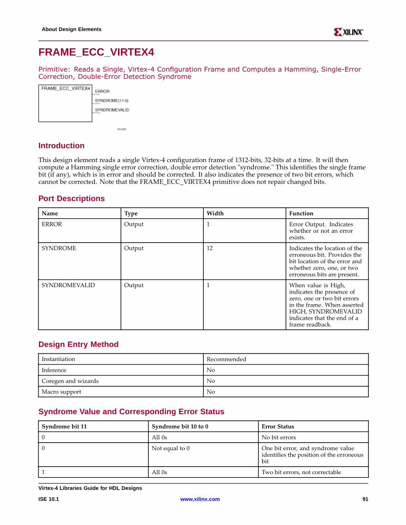
About Design Elements
FRAME_ECC_VIRTEX4
Primitive: Reads a Single, Virtex-4 Configuration Frame and Computes a Hamming, Single-ErrorCorrection, Double-Error Detection Syndrome
Intr oduction
This design element reads a single Virtex-4 configuration frame of 1312-bits, 32-bits at a time. It will thencompute a Hamming single error correction, double error detection "syndrome." This identifies the single framebit (if any), which is in error and should be corrected. It also indicates the presence of two bit errors, whichcannot be corrected. Note that the FRAME_ECC_VIRTEX4 primitive does not repair changed bits.
Por t Descriptions
Name Type Width Function
ERROR Output 1 Error Output. Indicateswhether or not an errorexists.
SYNDROME Output 12 Indicates the location of theerroneous bit. Provides thebit location of the error andwhether zero, one, or twoerroneous bits are present.
SYNDROMEVALID Output 1 When value is High,indicates the presence ofzero, one or two bit errorsin the frame. When assertedHIGH, SYNDROMEVALIDindicates that the end of aframe readback.
Design Entr y Method
Instantiation Recommended
Inference No
Coregen and wizards No
Macro support No
Syndr ome Value and Corresponding Error Status
Syndrome bit 11 Syndrome bit 10 to 0 Error Status
0 All 0s No bit errors
0 Not equal to 0 One bit error, and syndrome valueidentifies the position of the erroneousbit
1 All 0s Two bit errors, not correctable
Vir tex-4 Libraries Guide for HDL Designs
ISE 10.1 www.xilinx.com 91
About Design Elements
Note SYNDROME_VALID must be HIGH for the values on the table above to be useful.
VHDL Instantiation Template
Unless they already exist, copy the following two statements and paste them before the entity declaration.Library UNISIM;use UNISIM.vcomponents.all;
-- FRAME_ECC_VIRTEX4: Configuration Frame Error Correction Circuitry-- Virtex-4-- Xilinx HDL Libraries Guide, version 10.1.2
FRAME_ECC_VIRTEX4_inst : FRAME_ECC_VIRTEX4port map (ERROR=> ERROR,SYNDROME=> SYNDROME,SYNDROMEVALID=> SYNDROMEVALID);
-- End of FRAME_ECC_VIRTEX4_inst instantiation
Verilog Instantiation Template
// FRAME_ECC_VIRTEX4: Configuration Frame Error Correction Circuitry// Virtex-4// Xilinx HDL Libraries Guide, version 10.1.2
FRAME_ECC_VIRTEX4FRAME_ECC_VIRTEX4_inst (.ERROR(ERROR), // 1-bit output indicating an error.SYNDROME(SYNDROME),// 12-bit output location of erroroneous bit.SYNDROMEVALID(SYNDROMEVALID)// 1-bit output indicating 0, 1 or 2 bit errors in frame);
// End of FRAME_ECC_VIRTEX4_inst instantiation
For More Information
• See the Virtex-4 User Guide.
• See the Virtex-4 Data Sheets.
Vir tex-4 Libraries Guide for HDL Designs
92 www.xilinx.com ISE 10.1
About Design Elements
GT11_CUSTOM
Primitive: RocketIO MGTs with 622 Mb/s to 11.1 Gb/s Data Rates, 8 to 24 Transceivers per FPGA,and 2.5 GHz 5.55 GHz VCO, Less Than 1ns RMS Jitter
Intr oduction
This design element is a RocketIO MGT. RocketIO MGTs have flexible, programmable features that allowa multi-gigabit serial transceiver to be easily integrated into any Virtex-4 design. These elements support thefollowing features:• 10.3 Gb/s data rates• 8to 24 transceivers per FPGA• 2.5 GHz – 5.55 GHz VCO, less than 1ns RMS jitter• Transmitter pre-emphasis• Receiver continuous time equalization• On-chip AC coupled receiver, with optional by-pass• Receiver signal detect and loss of signal indicator, out of band signal receiver• Transmit driver idle state for out of band signaling-both outputs at Vcm• 8B/10B or 64B/66B encoding, or no data encoding (pass through mode)• Channel bonding• Flexible Cyclic Redundancy Check (CRC) generation and checking• Pins for transmitter and receiver termination voltage• You can reconfigure, using the secondary (dynamic) configuration bus• Multiple loopback paths including PMA RX-TX path
RocketIO MGTs are only available in FX devices.
Logic Table
Inputs Outputs
CHBONDI [4:0] DRDY
CSUPMARESET RXBUFERR
DADDR [7:0] RXCALFAIL
DCLK RXCOMMADET
DEN RXCYCLELIMIT
DI [15:0] RXLOCK
DWE RXRealIGN
ENCHANSYNC RXRECCLK1
ENMCOMMAALIGN RXBCLK
ENPCOMMAALIGN RXRECCLK2
GREFCLK RXSIGDET
LOOPBACK [1:0] TX1N
POWERDOWN TX1P
REFCLK1 TXBUFERR
REFCLK2 TXCALFAIL
Vir tex-4 Libraries Guide for HDL Designs
ISE 10.1 www.xilinx.com 93
About Design Elements
Inputs Outputs
RX1N TXCYCLELIMIT
RX1P TXLOCK
RXBLOCKSYNC64B66BUSE DO [15:0]
RXCLKSTABLE RXLOSSOFSYNC [1:0]
RXCOMMADETUSE RXCRCOUT [31:0]
RXCRCCLK TXCRCOUT [31:0]
RXCRCDATAVALID CHBONDO [4:0]
RXCRCDATAWIDTH [2:0] RXSTATUS [5:0]
RXCRCIN [63:0] RXDATA [63:0]
RXCRCINIT RXCHARISCOMMA [7:0]
RXCRCINTCLK RXCHARISK [7:0]
RXCRCPD RXDISPERR [7:0]
RXCRCRESET RXNOTINTABLE [7:0]
RXDATAWIDTH [1:0] RXRUNDISP [7:0]
RXDEC64B66BUSE TXRUNDISP [7:0]
RXDEC8B10BUSE TXKERR [7:0]
RXDESCRAM64B66BUSE
RXIGNOREBTF
RXINTDATAWIDTH [1:0]
RXPMARESET
RXPOLARITY
RXRESET
RXSLIDE
RXUSRCLK
RXUSRCLK2
TXBYPASS8B10B [7:0]
TXCHARDISPMODE [7:0]
TXCHARDISPVAL [7:0]
TXCHARISK [7:0]
TXCLKSTABLE
TXCRCCLK
TXCRCDATAVALID
TXCRCDATAWIDTH [2:0]
TXCRCIN [63:0]
TXCRCINIT
TXCRCINTCLK
TXCRCPD
TXCRCRESET
Vir tex-4 Libraries Guide for HDL Designs
94 www.xilinx.com ISE 10.1
About Design Elements
Inputs Outputs
TXDATA [63:0]
TXDATAWIDTH [1:0]
TXENC64B66BUSE
TXENC8B10BUSE
TXENOOB
TXGEARBOX64B66BUSE
TXINHIBIT
TXINTDATAWIDTH [1:0]
TXPMARESET
TXPOLARITY
TXRESET
TXSCRAM64B66BUSE
TXSYNC
TXUSRCLK
TXUSRCLK2
Design Entr y Method
Instantiation Yes
Inference No
Coregen and wizards Recommended
Macro support No
For More Information
• See the Virtex-4 User Guide.
• See the Virtex-4 Data Sheets.
Vir tex-4 Libraries Guide for HDL Designs
ISE 10.1 www.xilinx.com 95
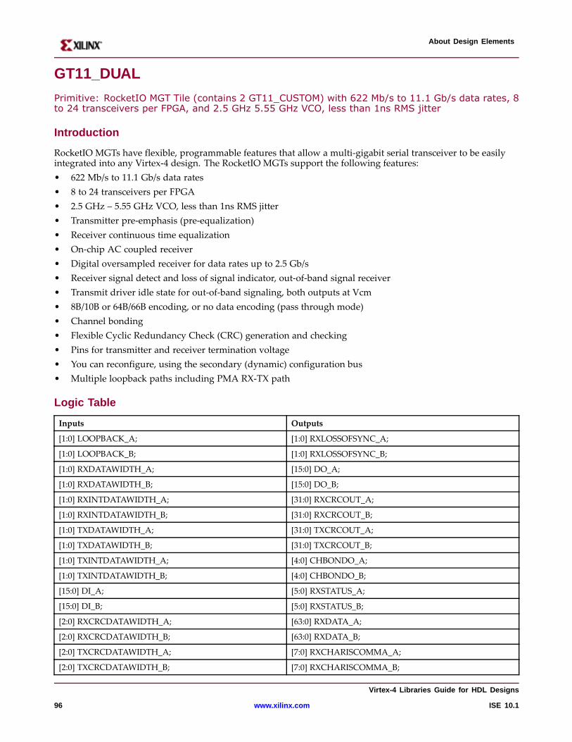
About Design Elements
GT11_DUAL
Primitive: RocketIO MGT Tile (contains 2 GT11_CUSTOM) with 622 Mb/s to 11.1 Gb/s data rates, 8to 24 transceivers per FPGA, and 2.5 GHz 5.55 GHz VCO, less than 1ns RMS jitter
Intr oduction
RocketIO MGTs have flexible, programmable features that allow a multi-gigabit serial transceiver to be easilyintegrated into any Virtex-4 design. The RocketIO MGTs support the following features:• 622 Mb/s to 11.1 Gb/s data rates• 8 to 24 transceivers per FPGA• 2.5 GHz – 5.55 GHz VCO, less than 1ns RMS jitter• Transmitter pre-emphasis (pre-equalization)• Receiver continuous time equalization• On-chip AC coupled receiver• Digital oversampled receiver for data rates up to 2.5 Gb/s• Receiver signal detect and loss of signal indicator, out-of-band signal receiver• Transmit driver idle state for out-of-band signaling, both outputs at Vcm• 8B/10B or 64B/66B encoding, or no data encoding (pass through mode)• Channel bonding• Flexible Cyclic Redundancy Check (CRC) generation and checking• Pins for transmitter and receiver termination voltage• You can reconfigure, using the secondary (dynamic) configuration bus• Multiple loopback paths including PMA RX-TX path
Logic Table
Inputs Outputs
[1:0] LOOPBACK_A; [1:0] RXLOSSOFSYNC_A;
[1:0] LOOPBACK_B; [1:0] RXLOSSOFSYNC_B;
[1:0] RXDATAWIDTH_A; [15:0] DO_A;
[1:0] RXDATAWIDTH_B; [15:0] DO_B;
[1:0] RXINTDATAWIDTH_A; [31:0] RXCRCOUT_A;
[1:0] RXINTDATAWIDTH_B; [31:0] RXCRCOUT_B;
[1:0] TXDATAWIDTH_A; [31:0] TXCRCOUT_A;
[1:0] TXDATAWIDTH_B; [31:0] TXCRCOUT_B;
[1:0] TXINTDATAWIDTH_A; [4:0] CHBONDO_A;
[1:0] TXINTDATAWIDTH_B; [4:0] CHBONDO_B;
[15:0] DI_A; [5:0] RXSTATUS_A;
[15:0] DI_B; [5:0] RXSTATUS_B;
[2:0] RXCRCDATAWIDTH_A; [63:0] RXDATA_A;
[2:0] RXCRCDATAWIDTH_B; [63:0] RXDATA_B;
[2:0] TXCRCDATAWIDTH_A; [7:0] RXCHARISCOMMA_A;
[2:0] TXCRCDATAWIDTH_B; [7:0] RXCHARISCOMMA_B;
Vir tex-4 Libraries Guide for HDL Designs
96 www.xilinx.com ISE 10.1
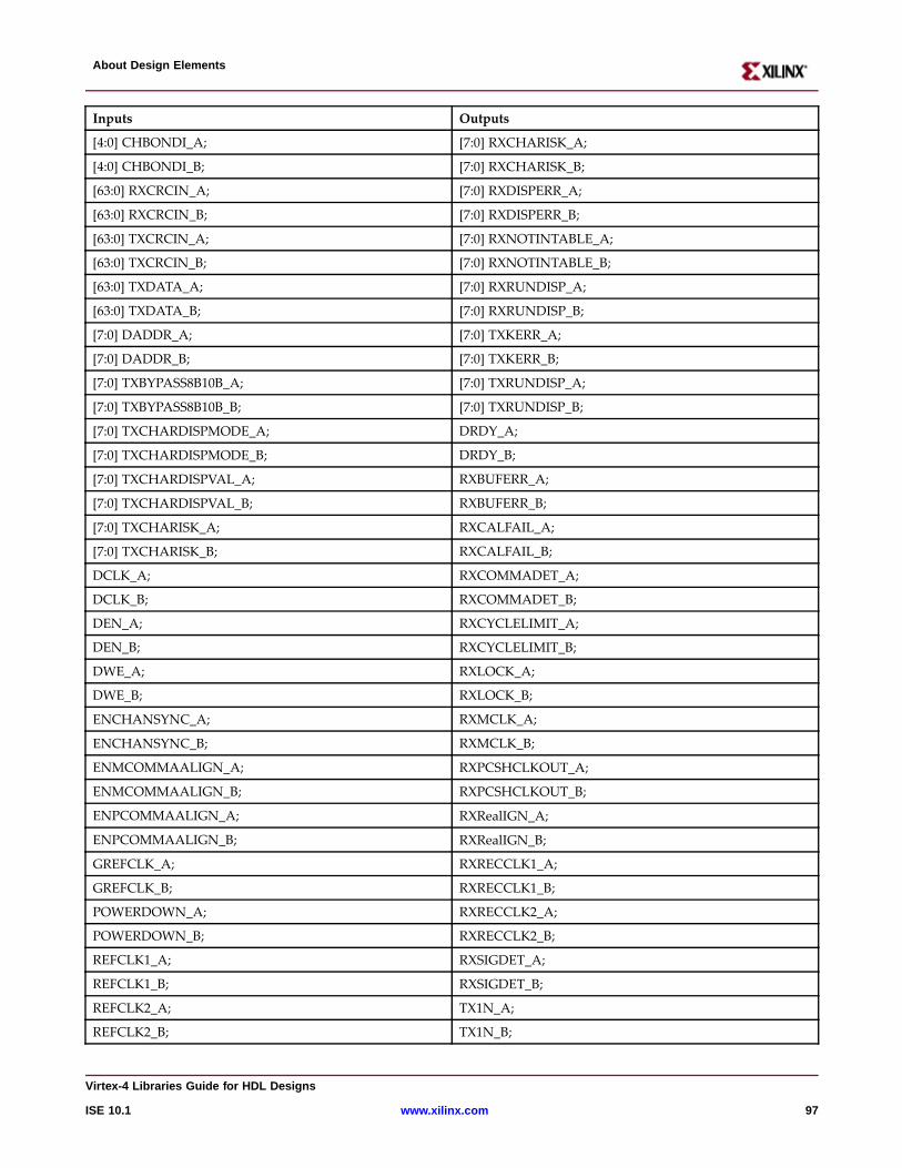
About Design Elements
Inputs Outputs
[4:0] CHBONDI_A; [7:0] RXCHARISK_A;
[4:0] CHBONDI_B; [7:0] RXCHARISK_B;
[63:0] RXCRCIN_A; [7:0] RXDISPERR_A;
[63:0] RXCRCIN_B; [7:0] RXDISPERR_B;
[63:0] TXCRCIN_A; [7:0] RXNOTINTABLE_A;
[63:0] TXCRCIN_B; [7:0] RXNOTINTABLE_B;
[63:0] TXDATA_A; [7:0] RXRUNDISP_A;
[63:0] TXDATA_B; [7:0] RXRUNDISP_B;
[7:0] DADDR_A; [7:0] TXKERR_A;
[7:0] DADDR_B; [7:0] TXKERR_B;
[7:0] TXBYPASS8B10B_A; [7:0] TXRUNDISP_A;
[7:0] TXBYPASS8B10B_B; [7:0] TXRUNDISP_B;
[7:0] TXCHARDISPMODE_A; DRDY_A;
[7:0] TXCHARDISPMODE_B; DRDY_B;
[7:0] TXCHARDISPVAL_A; RXBUFERR_A;
[7:0] TXCHARDISPVAL_B; RXBUFERR_B;
[7:0] TXCHARISK_A; RXCALFAIL_A;
[7:0] TXCHARISK_B; RXCALFAIL_B;
DCLK_A; RXCOMMADET_A;
DCLK_B; RXCOMMADET_B;
DEN_A; RXCYCLELIMIT_A;
DEN_B; RXCYCLELIMIT_B;
DWE_A; RXLOCK_A;
DWE_B; RXLOCK_B;
ENCHANSYNC_A; RXMCLK_A;
ENCHANSYNC_B; RXMCLK_B;
ENMCOMMAALIGN_A; RXPCSHCLKOUT_A;
ENMCOMMAALIGN_B; RXPCSHCLKOUT_B;
ENPCOMMAALIGN_A; RXRealIGN_A;
ENPCOMMAALIGN_B; RXRealIGN_B;
GREFCLK_A; RXRECCLK1_A;
GREFCLK_B; RXRECCLK1_B;
POWERDOWN_A; RXRECCLK2_A;
POWERDOWN_B; RXRECCLK2_B;
REFCLK1_A; RXSIGDET_A;
REFCLK1_B; RXSIGDET_B;
REFCLK2_A; TX1N_A;
REFCLK2_B; TX1N_B;
Vir tex-4 Libraries Guide for HDL Designs
ISE 10.1 www.xilinx.com 97

About Design Elements
Inputs Outputs
RX1N_A; TX1P_A;
RX1N_B; TX1P_B;
RX1P_A; TXBUFERR_A;
RX1P_B; TXBUFERR_B;
RXBLOCKSYNC64B66BUSE_A; TXCALFAIL_A;
RXBLOCKSYNC64B66BUSE_B; TXCALFAIL_B;
RXCLKSTABLE_A; TXCYCLELIMIT_A;
RXCLKSTABLE_B; TXCYCLELIMIT_B;
RXCOMMADETUSE_A; TXLOCK_A;
RXCOMMADETUSE_B; TXLOCK_B;
RXCRCCLK_A; TXOUTCLK1_A;
RXCRCCLK_B; TXOUTCLK1_B;
RXCRCDATAVALID_A; TXOUTCLK2_A;
RXCRCDATAVALID_B; TXOUTCLK2_B;
RXCRCINIT_A; TXPCSHCLKOUT_A;
RXCRCINIT_B; TXPCSHCLKOUT_B;
RXCRCINTCLK_A;
RXCRCINTCLK_B;
RXCRCPD_A;
RXCRCPD_B;
RXCRCRESET_A;
RXCRCRESET_B;
RXDEC64B66BUSE_A;
RXDEC64B66BUSE_B;
RXDEC8B10BUSE_A;
RXDEC8B10BUSE_B;
RXDESCRAM64B66BUSE_A;
RXDESCRAM64B66BUSE_B;
RXIGNOREBTF_A;
RXIGNOREBTF_B;
RXPMARESET_A;
RXPMARESET_B;
RXPOLARITY_A;
RXPOLARITY_B;
RXRESET_A;
RXRESET_B;
RXSLIDE_A;
RXSLIDE_B;
Vir tex-4 Libraries Guide for HDL Designs
98 www.xilinx.com ISE 10.1
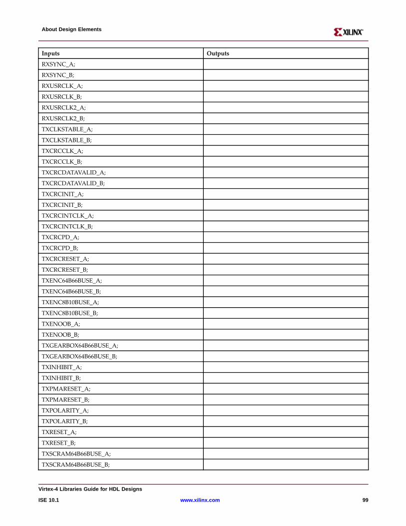
About Design Elements
Inputs Outputs
RXSYNC_A;
RXSYNC_B;
RXUSRCLK_A;
RXUSRCLK_B;
RXUSRCLK2_A;
RXUSRCLK2_B;
TXCLKSTABLE_A;
TXCLKSTABLE_B;
TXCRCCLK_A;
TXCRCCLK_B;
TXCRCDATAVALID_A;
TXCRCDATAVALID_B;
TXCRCINIT_A;
TXCRCINIT_B;
TXCRCINTCLK_A;
TXCRCINTCLK_B;
TXCRCPD_A;
TXCRCPD_B;
TXCRCRESET_A;
TXCRCRESET_B;
TXENC64B66BUSE_A;
TXENC64B66BUSE_B;
TXENC8B10BUSE_A;
TXENC8B10BUSE_B;
TXENOOB_A;
TXENOOB_B;
TXGEARBOX64B66BUSE_A;
TXGEARBOX64B66BUSE_B;
TXINHIBIT_A;
TXINHIBIT_B;
TXPMARESET_A;
TXPMARESET_B;
TXPOLARITY_A;
TXPOLARITY_B;
TXRESET_A;
TXRESET_B;
TXSCRAM64B66BUSE_A;
TXSCRAM64B66BUSE_B;
Vir tex-4 Libraries Guide for HDL Designs
ISE 10.1 www.xilinx.com 99
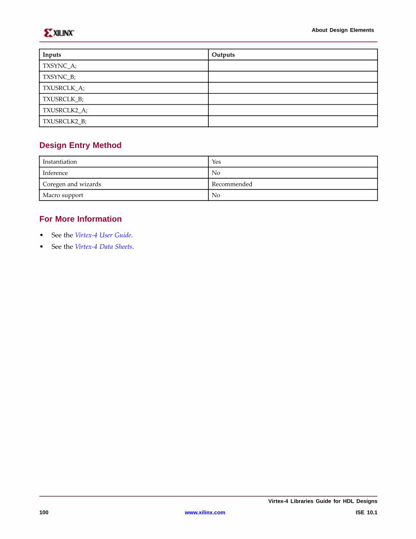
About Design Elements
Inputs Outputs
TXSYNC_A;
TXSYNC_B;
TXUSRCLK_A;
TXUSRCLK_B;
TXUSRCLK2_A;
TXUSRCLK2_B;
Design Entr y Method
Instantiation Yes
Inference No
Coregen and wizards Recommended
Macro support No
For More Information
• See the Virtex-4 User Guide.
• See the Virtex-4 Data Sheets.
Vir tex-4 Libraries Guide for HDL Designs
100 www.xilinx.com ISE 10.1
About Design Elements
GT11CLK
Primitive: A MUX That Can Select Fom Differential Package Input Clock, refclk From the Fabric, orrxbclk to Drive the Two Vertical Reference Clock Buses for the Column of MGTs
Intr oduction
This block needs to be instantiated when using the dedicated package pins for RocketIO clocks. There are twoavailable per MGT column.The attributes allow this package input to drive one or both SYNCLK clock trees.Please see the Virtex-4 RocketIO MGT User Guide for more details.
The attribute REFCLKSEL allows more clocking options. These options include: MGTCLK, SYNCLK1IN,SYNCLK2IN, REFCLK, RXBCLK.
Por t Descriptions
Inputs are MGTCLKP, MGTCLKN
Outputs are SYNCLK1OUT, SYNCLK2OUT
Design Entr y Method
Instantiation Yes
Inference No
Coregen and wizards Recommended
Macro support No
For More Information
• See the Virtex-4 User Guide.
• See the Virtex-4 Data Sheets.
Vir tex-4 Libraries Guide for HDL Designs
ISE 10.1 www.xilinx.com 101
About Design Elements
GT11CLK_MGT
Primitive: Allows Differential Package Input to Drive the Two Vertical Reference Clock Buses forthe Column of MGTs
Intr oduction
This block needs to be instantiated when using the dedicated package pins for RocketIO clocks. There are twoavailable per MGT column.The attributes allow this package input to drive one or both SYNCLK clock trees.Please see the Virtex-4 RocketIO MGT User Guide for more details. This design element is also available and hasan attribute REFCLKSEL, with the following VALUE options: MGTCLK, SYNCLK1IN, SYNCLK2IN, REFCLK,RXBCLK. This block allows more clocking options for MGTs.
Por t Description
Inputs are MGTCLKP, MGTCLKN
Outputs are SYNCLK1OUT, SYNCLK2OUT
Design Entr y Method
Instantiation Yes
Inference No
Coregen and wizards Recommended
Macro support No
For More Information
• See the Virtex-4 User Guide.
• See the Virtex-4 Data Sheets.
Vir tex-4 Libraries Guide for HDL Designs
102 www.xilinx.com ISE 10.1
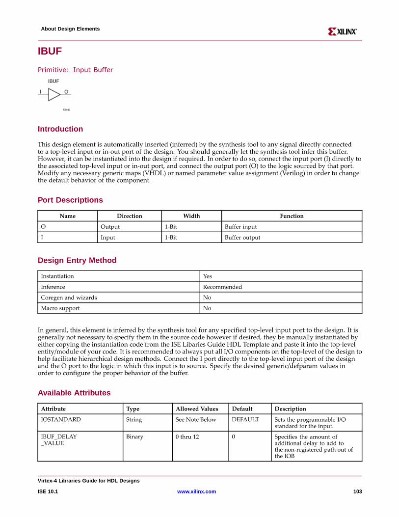
About Design Elements
IBUF
Primitive: Input Buffer
Intr oduction
This design element is automatically inserted (inferred) by the synthesis tool to any signal directly connectedto a top-level input or in-out port of the design. You should generally let the synthesis tool infer this buffer.However, it can be instantiated into the design if required. In order to do so, connect the input port (I) directly tothe associated top-level input or in-out port, and connect the output port (O) to the logic sourced by that port.Modify any necessary generic maps (VHDL) or named parameter value assignment (Verilog) in order to changethe default behavior of the component.
Por t Descriptions
Name Direction Width Function
O Output 1-Bit Buffer input
I Input 1-Bit Buffer output
Design Entr y Method
Instantiation Yes
Inference Recommended
Coregen and wizards No
Macro support No
In general, this element is inferred by the synthesis tool for any specified top-level input port to the design. It isgenerally not necessary to specify them in the source code however if desired, they be manually instantiated byeither copying the instantiation code from the ISE Libaries Guide HDL Template and paste it into the top-levelentity/module of your code. It is recommended to always put all I/O components on the top-level of the design tohelp facilitate hierarchical design methods. Connect the I port directly to the top-level input port of the designand the O port to the logic in which this input is to source. Specify the desired generic/defparam values inorder to configure the proper behavior of the buffer.
Availab le Attrib utes
Attribute Type Allowed Values Default Description
IOSTANDARD String See Note Below DEFAULT Sets the programmable I/Ostandard for the input.
IBUF_DELAY_VALUE
Binary 0 thru 12 0 Specifies the amount ofadditional delay to add tothe non-registered path out ofthe IOB
Vir tex-4 Libraries Guide for HDL Designs
ISE 10.1 www.xilinx.com 103
About Design Elements
Attribute Type Allowed Values Default Description
IFD_DELAY_VALUE
Binary AUTO, 0 thru 6 AUTO Specifies the amount ofadditional delay to add tothe registered path within theIOB
Note Consult the device user guide or databook for the allowed values and the default value.
VHDL Instantiation Template
Unless they already exist, copy the following two statements and paste them before the entity declaration.Library UNISIM;use UNISIM.vcomponents.all;
-- IBUF: Single-ended Input Buffer-- All devices-- Xilinx HDL Libraries Guide, version 10.1.2
IBUF_inst : IBUFgeneric map (IBUF_DELAY_VALUE => "0", -- Specify the amount of added input delay for buffer, "0"-"16" (Spartan-3E/3A only)IFD_DELAY_VALUE => "AUTO", -- Specify the amount of added delay for input register, "AUTO", "0"-"8" (Spartan-3E/3A only)IOSTANDARD=> "DEFAULT")port map (O => O, -- Buffer outputI => I -- Buffer input (connect directly to top-level port));
-- End of IBUF_inst instantiation
Verilog Instantiation Template
// IBUF: Single-ended Input Buffer// All devices// Xilinx HDL Libraries Guide, version 10.1.2
IBUF #(.IBUF_DELAY_VALUE("0"), // Specify the amount of added input delay for// the buffer, "0"-"16" (Spartan-3E/3A only).IFD_DELAY_VALUE("AUTO"), // Specify the amount of added delay for input// register, "AUTO", "0"-"8" (Spartan-3E/3A only).IOSTANDARD("DEFAULT") // Specify the input I/O standard)IBUF_inst (.O(O), // Buffer output.I(I) // Buffer input (connect directly to top-level port));
// End of IBUF_inst instantiation
Vir tex-4 Libraries Guide for HDL Designs
104 www.xilinx.com ISE 10.1

About Design Elements
For More Information
• See the Virtex-4 User Guide.
• See the Virtex-4 Data Sheets.
Vir tex-4 Libraries Guide for HDL Designs
ISE 10.1 www.xilinx.com 105
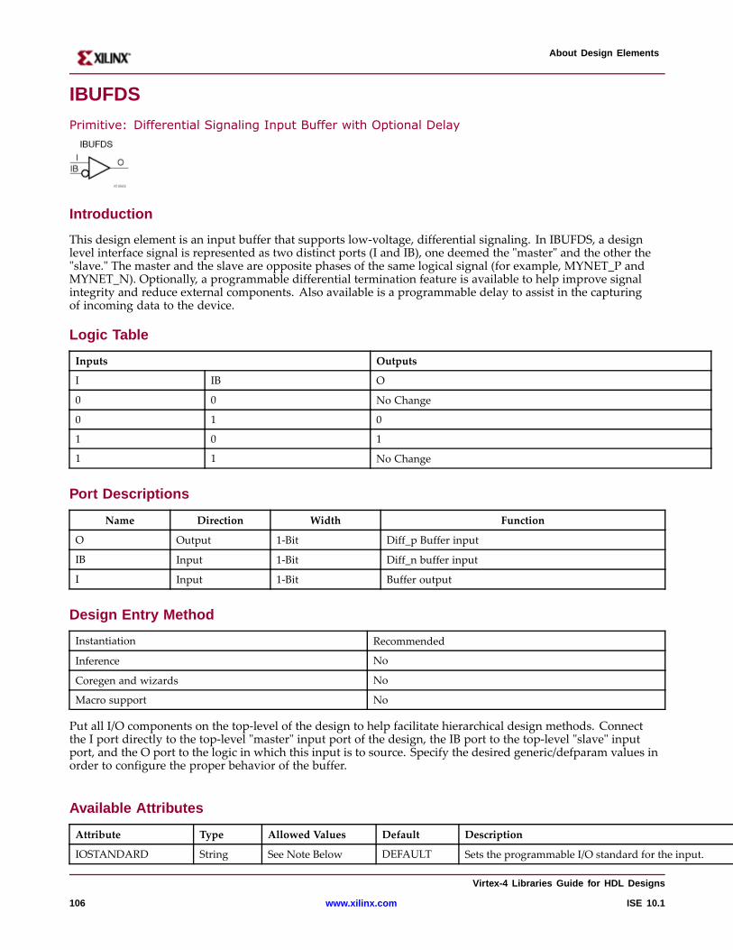
About Design Elements
IBUFDS
Primitive: Differential Signaling Input Buffer with Optional Delay
Intr oduction
This design element is an input buffer that supports low-voltage, differential signaling. In IBUFDS, a designlevel interface signal is represented as two distinct ports (I and IB), one deemed the "master" and the other the"slave." The master and the slave are opposite phases of the same logical signal (for example, MYNET_P andMYNET_N). Optionally, a programmable differential termination feature is available to help improve signalintegrity and reduce external components. Also available is a programmable delay to assist in the capturingof incoming data to the device.
Logic Table
Inputs Outputs
I IB O
0 0 No Change
0 1 0
1 0 1
1 1 No Change
Por t Descriptions
Name Direction Width Function
O Output 1-Bit Diff_p Buffer input
IB Input 1-Bit Diff_n buffer input
I Input 1-Bit Buffer output
Design Entr y Method
Instantiation Recommended
Inference No
Coregen and wizards No
Macro support No
Put all I/O components on the top-level of the design to help facilitate hierarchical design methods. Connectthe I port directly to the top-level "master" input port of the design, the IB port to the top-level "slave" inputport, and the O port to the logic in which this input is to source. Specify the desired generic/defparam values inorder to configure the proper behavior of the buffer.
Availab le Attrib utes
Attribute Type Allowed Values Default Description
IOSTANDARD String See Note Below DEFAULT Sets the programmable I/O standard for the input.
Vir tex-4 Libraries Guide for HDL Designs
106 www.xilinx.com ISE 10.1
About Design Elements
Attribute Type Allowed Values Default Description
IBUF_DELAY_VALUE
Binary 0 thru 12 0 Specifies the amount of additional delay to add to thenon-registered path out of the IOB
IFD_DELAY_VALUE
Binary AUTO, 0 thru 6 AUTO Specifies the amount of additional delay to add to theregistered path within the IOB
DIFF_TERM Boolean TRUE or FALSE FALSE Enables the built-in differential termination resistor.
Note Consult the device user guide or databook for the allowed values and the default value.
VHDL Instantiation Template
Unless they already exist, copy the following two statements and paste them before the entity declaration.Library UNISIM;use UNISIM.vcomponents.all;
-- IBUFDS: Differential Input Buffer-- Virtex-II/II-Pro, Spartan-3/3E/3A-- Xilinx HDL Libraries Guide, version 10.1.2
IBUFDS_inst : IBUFDSgeneric map (CAPACITANCE=> "DONT_CARE", -- "LOW", "NORMAL", "DONT_CARE" (Virtex-4 only)DIFF_TERM => FALSE, -- Differential Termination (Virtex-4/5, Spartan-3E/3A)IBUF_DELAY_VALUE => "0", -- Specify the amount of added input delay for buffer, "0"-"16" (Spartan-3E/3A only)IFD_DELAY_VALUE => "AUTO", -- Specify the amount of added delay for input register, "AUTO", "0"-"8" (Spartan-3E/3A only)IOSTANDARD=> "DEFAULT")port map (O => O, -- Clock buffer outputI => I, -- Diff_p clock buffer input (connect directly to top-level port)IB => IB -- Diff_n clock buffer input (connect directly to top-level port));
-- End of IBUFDS_inst instantiation
Verilog Instantiation Template
// IBUFDS: Differential Input Buffer// Virtex-II/II-Pro/4/5, Spartan-3/3E/3A// Xilinx HDL Libraries Guide, version 10.1.2
IBUFDS #(.CAPACITANCE("DONT_CARE"), // "LOW", "NORMAL", "DONT_CARE" (Virtex-4 only).DIFF_TERM("FALSE"), // Differential Termination (Virtex-4/5, Spartan-3E/3A).IBUF_DELAY_VALUE("0"), // Specify the amount of added input delay for// the buffer, "0"-"16" (Spartan-3E only).IFD_DELAY_VALUE("AUTO"), // Specify the amount of added delay for input// register, "AUTO", "0"-"8" (Spartan-3E/3A only).IOSTANDARD("DEFAULT") // Specify the input I/O standard) IBUFDS_inst (.O(O), // Buffer output.I(I), // Diff_p buffer input (connect directly to top-level port).IB(IB) // Diff_n buffer input (connect directly to top-level port));
// End of IBUFDS_inst instantiation
For More Information
• See the Virtex-4 User Guide.• See the Virtex-4 Data Sheets.
Vir tex-4 Libraries Guide for HDL Designs
ISE 10.1 www.xilinx.com 107
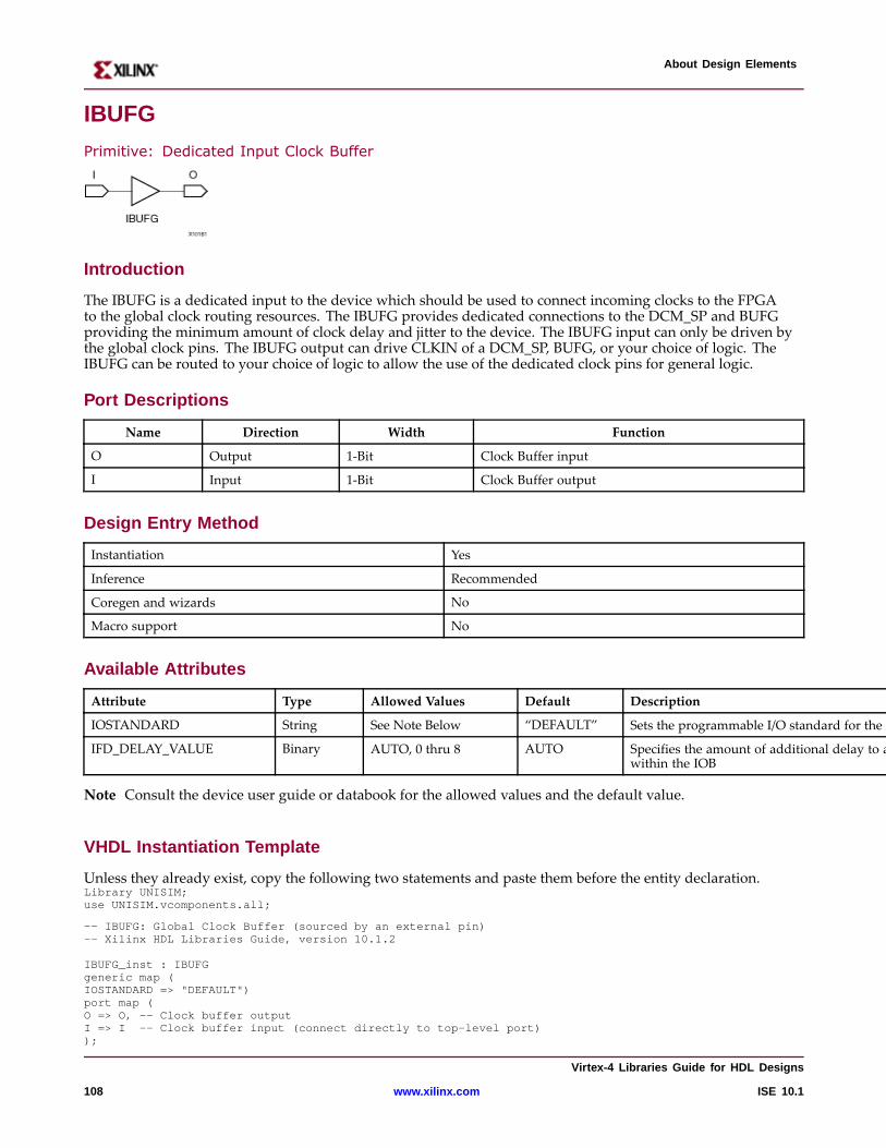
About Design Elements
IBUFG
Primitive: Dedicated Input Clock Buffer
Intr oduction
The IBUFG is a dedicated input to the device which should be used to connect incoming clocks to the FPGAto the global clock routing resources. The IBUFG provides dedicated connections to the DCM_SP and BUFGproviding the minimum amount of clock delay and jitter to the device. The IBUFG input can only be driven bythe global clock pins. The IBUFG output can drive CLKIN of a DCM_SP, BUFG, or your choice of logic. TheIBUFG can be routed to your choice of logic to allow the use of the dedicated clock pins for general logic.
Por t Descriptions
Name Direction Width Function
O Output 1-Bit Clock Buffer input
I Input 1-Bit Clock Buffer output
Design Entr y Method
Instantiation Yes
Inference Recommended
Coregen and wizards No
Macro support No
Availab le Attrib utes
Attribute Type Allowed Values Default Description
IOSTANDARD String See Note Below “DEFAULT” Sets the programmable I/O standard for the input.
IFD_DELAY_VALUE Binary AUTO, 0 thru 8 AUTO Specifies the amount of additional delay to add to the registered pathwithin the IOB
Note Consult the device user guide or databook for the allowed values and the default value.
VHDL Instantiation Template
Unless they already exist, copy the following two statements and paste them before the entity declaration.Library UNISIM;use UNISIM.vcomponents.all;
-- IBUFG: Global Clock Buffer (sourced by an external pin)-- Xilinx HDL Libraries Guide, version 10.1.2
IBUFG_inst : IBUFGgeneric map (IOSTANDARD=> "DEFAULT")port map (O => O, -- Clock buffer outputI => I -- Clock buffer input (connect directly to top-level port));
Vir tex-4 Libraries Guide for HDL Designs
108 www.xilinx.com ISE 10.1
About Design Elements
-- End of IBUFG_inst instantiation
Verilog Instantiation Template
// IBUFG: Global Clock Buffer (sourced by an external pin)// All FPGAs// Xilinx HDL Libraries Guide, version 10.1.2
IBUFG #(.IOSTANDARD("DEFAULT")) IBUFG_inst (.O(O), // Clock buffer output.I(I) // Clock buffer input (connect directly to top-level port));
// End of IBUFG_inst instantiation
For More Information
• See the Virtex-4 User Guide.
• See the Virtex-4 Data Sheets.
Vir tex-4 Libraries Guide for HDL Designs
ISE 10.1 www.xilinx.com 109
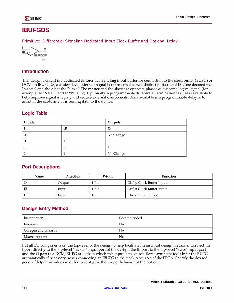
About Design Elements
IBUFGDS
Primitive: Differential Signaling Dedicated Input Clock Buffer and Optional Delay
Intr oduction
This design element is a dedicated differential signaling input buffer for connection to the clock buffer (BUFG) orDCM. In IBUFGDS, a design-level interface signal is represented as two distinct ports (I and IB), one deemed the"master" and the other the "slave." The master and the slave are opposite phases of the same logical signal (forexample, MYNET_P and MYNET_N). Optionally, a programmable differential termination feature is available tohelp improve signal integrity and reduce external components. Also available is a programmable delay is toassist in the capturing of incoming data to the device.
Logic Table
Inputs Outputs
I IB O
0 0 No Change
0 1 0
1 0 1
1 1 No Change
Por t Descriptions
Name Direction Width Function
O Output 1-Bit Diff_p Clock Buffer Input
IB Input 1-Bit Diff_n Clock Buffer Input
I Input 1-Bit Clock Buffer output
Design Entr y Method
Instantiation Recommended
Inference No
Coregen and wizards No
Macro support No
Put all I/O components on the top-level of the design to help facilitate hierarchical design methods. Connect theI port directly to the top-level "master" input port of the design, the IB port to the top-level "slave" input portand the O port to a DCM, BUFG or logic in which this input is to source. Some synthesis tools infer the BUFGautomatically if necessary, when connecting an IBUFG to the clock resources of the FPGA. Specify the desiredgeneric/defparam values in order to configure the proper behavior of the buffer.
Vir tex-4 Libraries Guide for HDL Designs
110 www.xilinx.com ISE 10.1
About Design Elements
Availab le Attrib utes
Attribute Type Allowed Values Default Description
IOSTANDARD String See Note Below “DEFAULT” Sets the programmable I/O standard for the input.
IFD_DELAY_VALUE Binary AUTO, 0 thru 6 AUTO Specifies the amount of additional delay to add to theregistered path within the IOB.
DIFF_TERM Boolean TRUE or FALSE FALSE Enables the built-in differential termination resistor.
Note Consult the device user guide or databook for the allowed values and the default value.
VHDL Instantiation Template
Unless they already exist, copy the following two statements and paste them before the entity declaration.Library UNISIM;use UNISIM.vcomponents.all;
-- IBUFGDS: Differential Global Clock Buffer (sourced by an external pin)-- Virtex-II/II-Pro/4/5, Spartan-3/3E/3A-- Xilinx HDL Libraries Guide, version 10.1.2
IBUFGDS_inst : IBUFGDSgeneric map (IOSTANDARD=> "DEFAULT")port map (O => O, -- Clock buffer outputI => I, -- Diff_p clock buffer inputIB => IB -- Diff_n clock buffer input);
-- End of IBUFGDS_inst instantiation
Verilog Instantiation Template
// IBUFGDS: Differential Global Clock Buffer (sourced by an external pin)// Virtex-II/II-Pro/4/5, Spartan-3/3E/3A// Xilinx HDL Libraries Guide, version 10.1.2
IBUFGDS #(.DIFF_TERM("FALSE"), // Differential Termination (Virtex-4/5, Spartan-3E/3A).IOSTANDARD("DEFAULT") // Specifies the I/O standard for this buffer) IBUFGDS_inst (.O(O), // Clock buffer output.I(I), // Diff_p clock buffer input.IB(IB) // Diff_n clock buffer input);
// End of IBUFGDS_inst instantiation
Vir tex-4 Libraries Guide for HDL Designs
ISE 10.1 www.xilinx.com 111

About Design Elements
For More Information
• See the Virtex-4 User Guide.
• See the Virtex-4 Data Sheets.
Vir tex-4 Libraries Guide for HDL Designs
112 www.xilinx.com ISE 10.1
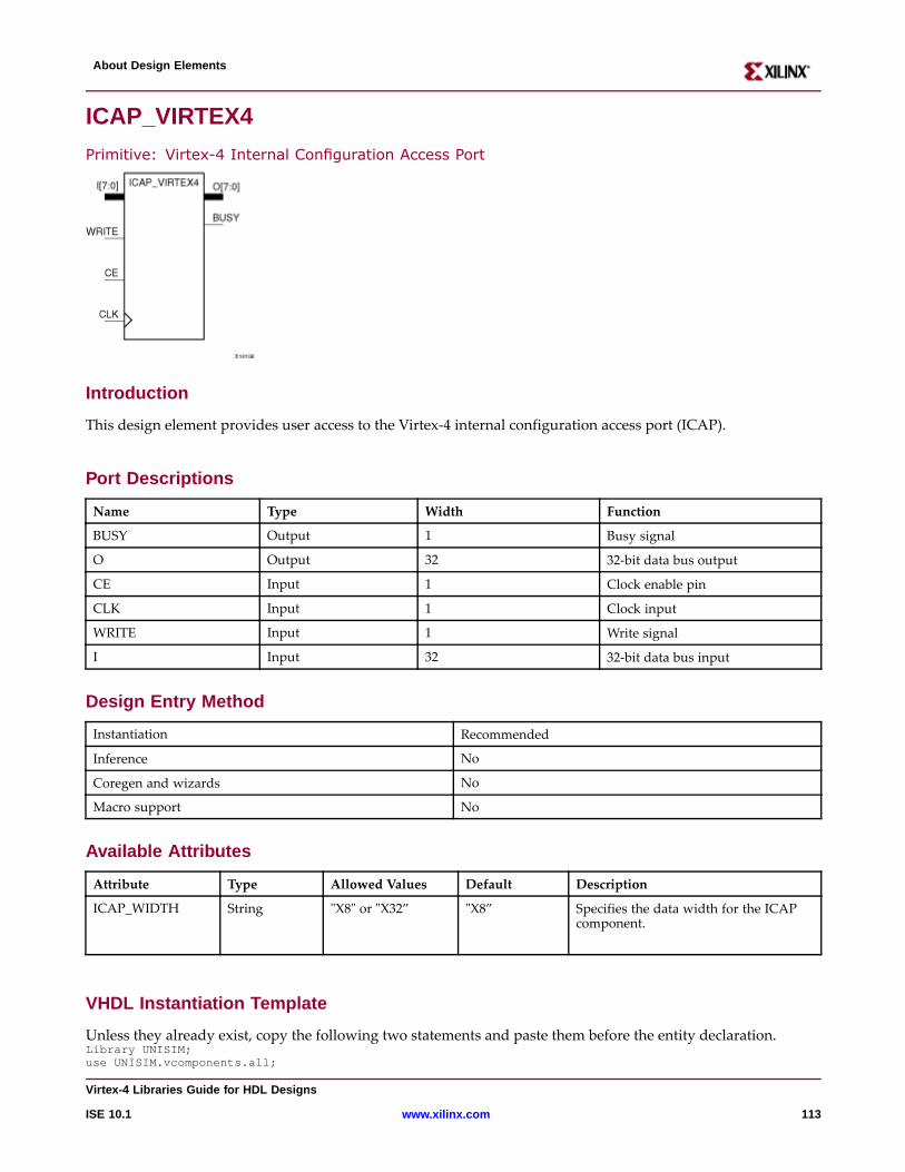
About Design Elements
ICAP_VIRTEX4
Primitive: Virtex-4 Internal Configuration Access Port
Intr oduction
This design element provides user access to the Virtex-4 internal configuration access port (ICAP).
Por t Descriptions
Name Type Width Function
BUSY Output 1 Busy signal
O Output 32 32-bit data bus output
CE Input 1 Clock enable pin
CLK Input 1 Clock input
WRITE Input 1 Write signal
I Input 32 32-bit data bus input
Design Entr y Method
Instantiation Recommended
Inference No
Coregen and wizards No
Macro support No
Availab le Attrib utes
Attribute Type Allowed Values Default Description
ICAP_WIDTH String "X8" or "X32” "X8” Specifies the data width for the ICAPcomponent.
VHDL Instantiation Template
Unless they already exist, copy the following two statements and paste them before the entity declaration.Library UNISIM;use UNISIM.vcomponents.all;
Vir tex-4 Libraries Guide for HDL Designs
ISE 10.1 www.xilinx.com 113
About Design Elements
-- ICAP_VIRTEX4: Internal Configuration Access Port-- Virtex-4-- Xilinx HDL Libraries Guide, version 10.1.2
ICAP_VIRTEX4_inst : ICAP_VIRTEX4generic map (ICAP_WIDTH => "X8") -- "X8" or "X32"port map (BUSY => BUSY, -- Busy outputO => O, -- 32-bit data outputCE => CE, -- Clock enable inputCLK => CLK, -- Clock inputI => I, -- 32-bit data inputWRITE => WRITE -- Write input);
-- End of ICAP_VIRTEX4_inst instantiation
Verilog Instantiation Template
// ICAP_VIRTEX4: Internal Configuration Access Port// Virtex-4// Xilinx HDL Libraries Guide, version 10.1.2
ICAP_VIRTEX4 #(.ICAP_WIDTH("X8") // "X8" or "X32") ICAP_VIRTEX4_inst (.BUSY(BUSY), // Busy output.O(O), // 32-bit data output.CE(CE), // Clock enable input.CLK(CLK), // Clock input.I(I), // 32-bit data input.WRITE(WRITE) // Write input);
// End of ICAP_VIRTEX4_inst instantiation
For More Information
• See the Virtex-4 User Guide.
• See the Virtex-4 Data Sheets.
Vir tex-4 Libraries Guide for HDL Designs
114 www.xilinx.com ISE 10.1
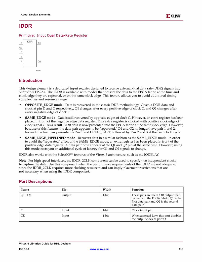
About Design Elements
IDDR
Primitive: Input Dual Data-Rate Register
Intr oduction
This design element is a dedicated input register designed to receive external dual data rate (DDR) signals intoVirtex™-5 FPGAs. The IDDR is available with modes that present the data to the FPGA fabric at the time andclock edge they are captured, or on the same clock edge. This feature allows you to avoid additional timingcomplexities and resource usage.
• OPPOSITE_EDGE mode - Data is recovered in the classic DDR methodology. Given a DDR data andclock at pin D and C respectively, Q1 changes after every positive edge of clock C, and Q2 changes afterevery negative edge of clock C.
• SAME_EDGEmode -Data is still recovered by opposite edges of clock C. However, an extra register has beenplaced in front of the negative edge data register. This extra register is clocked with positive clock edge ofclock signal C. As a result, DDR data is now presented into the FPGA fabric at the same clock edge. However,because of this feature, the data pair appears to be "separated." Q1 and Q2 no longer have pair 1 and 2.Instead, the first pair presented is Pair 1 and DONT_CARE, followed by Pair 2 and 3 at the next clock cycle.
• SAME_EDGE_PIPELINED mode - Recovers data in a similar fashion as the SAME_EDGE mode. In orderto avoid the "separated" effect of the SAME_EDGE mode, an extra register has been placed in front of thepositive edge data register. A data pair now appears at the Q1 and Q2 pin at the same time. However, usingthis mode costs you an additional cycle of latency for Q1 and Q2 signals to change.
IDDR also works with the SelectIO™ features of the Virtex-5 architecture, such as the IODELAY.
Note For high speed interfaces, the IDDR_2CLK component can be used to specify two independent clocksto capture the data. Use this component when the performance requirements of the IDDR are not adequate,since the IDDR_2CLK requires more clocking resources and can imply placement restrictions that arenot necessary when using the IDDR component.
Por t Descriptions
Name Dir Width Function
Q1 - Q2 Output 1-bit These pins are the IDDR output thatconnects to the FPGA fabric. Q1 is thefirst data pair and Q2 is the seconddata pair.
C Input 1-bit Clock input pin.
CE Input 1-bit When asserted Low, this port disablesthe output clock at port O.
Vir tex-4 Libraries Guide for HDL Designs
ISE 10.1 www.xilinx.com 115
About Design Elements
Name Dir Width Function
D Input 1-bit This pin is where the DDR data ispresented into the IDDR module.
This pin connects to a top-level inputor bi-directional port, and IODELAYconfigured for an input delay or toan appropriate input or bidirectionalbuffer.
R Input 1-bit Active high reset forcing Q1 and Q2to a logic zero. Can be synchronous orasynchronous based on the SRTYPEattribute.
S Input 1-bit Active high reset forcing Q1 and Q2to a logic one. Can be synchronous orasynchronous based on the SRTYPEattribute.
Design Entr y Method
Instantiation Recommended
Inference No
Coregen and wizards No
Macro support No
Availab le Attrib utes
Attribute Type Allowed Values Default Description
DDR_CLK_EDGE
String "OPPOSITE_EDGE","SAME_EDGE","SAME_EDGE_PIPELINED"
"OPPOSITE_EDGE”DDR clock mode recovery modeselection. See below for moreexplanation.
INIT_Q1 Binary 0 or 1 0 Initial value on the Q1 pin afterconfiguration startup or when GSR isasserted.
INIT_Q2 Binary 0 or 1 0 Initial value on the Q2 pin afterconfiguration startup or when GSR isasserted.
SRTYPE String "SYNC" or "ASYNC” "SYNC” Set/reset type selection. "SYNC"specifies the behavior of the reset (R)and set (S) pins to be synchronous tothe positive edge of the C clock pin."ASYNC" specifies an asynchronousset/reset function.
VHDL Instantiation Template
Unless they already exist, copy the following two statements and paste them before the entity declaration.Library UNISIM;use UNISIM.vcomponents.all;
-- IDDR: Double Data Rate Input Register with Set, Reset-- and Clock Enable.-- Virtex-4/5-- Xilinx HDL Libraries Guide, version 10.1.2
Vir tex-4 Libraries Guide for HDL Designs
116 www.xilinx.com ISE 10.1
About Design Elements
IDDR_inst : IDDRgeneric map (DDR_CLK_EDGE=> "OPPOSITE_EDGE", -- "OPPOSITE_EDGE", "SAME_EDGE"-- or "SAME_EDGE_PIPELINED"INIT_Q1 => ’0’, -- Initial value of Q1: ’0’ or ’1’INIT_Q2 => ’0’, -- Initial value of Q2: ’0’ or ’1’SRTYPE => "SYNC") -- Set/Reset type: "SYNC" or "ASYNC"port map (Q1 => Q1, -- 1-bit output for positive edge of clockQ2 => Q2, -- 1-bit output for negative edge of clockC => C, -- 1-bit clock inputCE => CE, -- 1-bit clock enable inputD => D, -- 1-bit DDR data inputR => R, -- 1-bit resetS => S -- 1-bit set);
-- End of IDDR_inst instantiation
Verilog Instantiation Template
// IDDR: Input Double Data Rate Input Register with Set, Reset// and Clock Enable.// Virtex-4/5// Xilinx HDL Libraries Guide, version 10.1.2
IDDR #(.DDR_CLK_EDGE("OPPOSITE_EDGE"), // "OPPOSITE_EDGE", "SAME_EDGE"// or "SAME_EDGE_PIPELINED".INIT_Q1(1’b0), // Initial value of Q1: 1’b0 or 1’b1.INIT_Q2(1’b0), // Initial value of Q2: 1’b0 or 1’b1.SRTYPE("SYNC") // Set/Reset type: "SYNC" or "ASYNC") IDDR_inst (.Q1(Q1), // 1-bit output for positive edge of clock.Q2(Q2), // 1-bit output for negative edge of clock.C(C), // 1-bit clock input.CE(CE), // 1-bit clock enable input.D(D), // 1-bit DDR data input.R(R), // 1-bit reset.S(S) // 1-bit set);
// End of IDDR_inst instantiation
For More Information
• See the Virtex-4 User Guide.
• See the Virtex-4 Data Sheets.
Vir tex-4 Libraries Guide for HDL Designs
ISE 10.1 www.xilinx.com 117

About Design Elements
IDELAY
Primitive: Input Delay Element
Intr oduction
Virtex™-4 and Virtex™-5 devices have an IDELAY module in the input path of every user I/O. IDELAY allowsthe implementation of deskew algorithms to correctly capture incoming data. IDELAY can be applied todata signals, clock signals, or both. IDELAY features a fully-controllable, 64-tap delay line. When used inconjunction with the IDELAYCTRL component circuitry, the IDELAY can provide precise time increments ofdelay independent of process, voltage, and temperature variations. Three modes of operation are available:• Zero hold time delay mode - This mode of operation allows backward compatibility for designs using the
zero-hold time delay feature in Virtex™-II, Virtex™-II Pro, Virtex™-4, and Virtex-5 devices. When used inthis mode, the IDELAYCTRL primitive does not need to be instantiated.
• Fixed tap-delay mode - In the fixed tap-delay mode, the delay value is set to the number determined bythe attribute IOBDELAY_VALUE. This value cannot be changed during run-time. When used in this mode,the IDELAYCTRL primitive must be instantiated.
• Variable tap-delay mode - In the variable tap-delay mode, the delay value can be changed at run-time bymanipulating the control signals CE and INC. When used in this mode, the IDELAYCTRL primitive must beinstantiated.
Por t Descriptions
Available Ports Direction Width Function
I Input 1 Serial input data from IOB
C Input 1 Clock input
INC Input 1 Increment/decrement number of tap delays
CE Input 1 Enable increment/decrement function
RST Input 1 Reset delay chain to pre-programmed value.If no value programmed, reset to 0.
O Output 1 Combinatorial output
Data Input and Output - I and O
IDELAY primitives are located in three different types of general purpose IOB locations. The input and outputconnectivity differs for each type of IOB location.• General Purpose IOBs - The input of IDELAY in a general-purpose IOB comes directly from the input
buffer, IBUF. The output of IDELAY (O) is connected directly to your logic. The input and output datapath iscombinatorial and is not affected by the clock signal (C). However, you can choose to register the outputsignal (O) in the IOB.
• Regional Clock-Capable IOBs - Regional clock-capable IOBs are located in one I/O pair directly above andbelow an HCLK IOB. The input of IDELAY in a regional clock-capable IOB comes directly from the inputbuffer, IBUF. The output of IDELAY in a regional clock-capable IOB can go to one of the following locations:– Directly to your logic
Vir tex-4 Libraries Guide for HDL Designs
118 www.xilinx.com ISE 10.1
About Design Elements
– BUFIO (in the case of a regional clock signal)
The regional clock buffer, BUFIO, connects the incoming regional clock signal to the regional I/O clock tree,IOCLK. BUFIO also connects to the regional clock buffer, BUFR to connect to the regional clock tree, rclk.The input and output datapath is combinatorial and is not affected by the clock signal (C). However, you canchoose to register the output signal (O) in the IOB.
• Global clock-capable IOBs - Global clock-capable IOBs are located in the center I/O column. The input ofthe IDELAY module in a global clock-capable IOB comes directly from the input global clock buffer, IBUFG.The output of the IDELAY module in a global clock-capable IOB can go to one of the following locations:
– Directly to your logic
– BUFG (in the case of a global clock signal)
The global clock buffer, BUFG, connects the incoming regional clock signal to the global clock tree, gclk. Theinput and output datapath is combinatorial and is not affected by the clock signal (C). However, you canchoose to register the output signal (O) in the IOB.
Clock Input - C
All control inputs to IDELAY (RST, CE and INC) are synchronous to the clock input (C). The data input andoutput (I and O) of IDELAY is not affected by this clock signal. This clock input is identical to the CLKDIV inputfor the ISERDES. All the clock sources used to drive CLKDIV can therefore drive the IDELAY clock input (C).The clock sources that can drive the clock input (C) are:
• Eight gclk (global clock tree)
• Two rclk (regional clock tree)
Module Reset - RST
The IDELAY reset signal, RST, resets the tap-delay line to a value set by the IOBDELAY_VALUE attribute. If theIOBDELAY_VALUE attribute is not specified, the tap-delay line is reset to 0.
Increment/Decrement Signals - CE, INC
The increment/decrement enable signal (CE) determines when the increment/decrement signal (INC) isactivated. INC determines whether to increment or decrement the tap-delay line. When CE = 0, the tap delayremains constant no matter what the value of INC. When CE = 1, the tap-delay value increments or decrementsdepending on the value of INC. The tap delay is incremented or decremented synchronously with respect tothe input clock (C). As long as CE = 1, the tap-delay increments or decrements by one every clock cycle. Theincrement/decrement operation is summarized in the following table:
Operation RST CE INC
Reset to configured value oftap count
1 x x
Increment tap count 0 1 1
Decrement tap count 0 1 0
No change 0 0 x
Note
1. RST resets delay chain to tap count specified by attribute IOBDELAY_VALUE. If IOBDELAY_VALUEis not specified, tap count reset to 0.
2. RST, CE, and INC are synchronous to the input clock signal (C).
When CE is raised, the increment/decrement operation begins on the next positive clock cycle. When CE islowered, the increment/decrement operation ceases on the next positive clock cycle.
Vir tex-4 Libraries Guide for HDL Designs
ISE 10.1 www.xilinx.com 119
About Design Elements
Design Entr y Method
Instantiation Recommended
Inference No
Coregen and wizards No
Macro support No
Availab le Attrib utes
Attribute Type Allowed Values Default Description
IOBDELAY_TYPE
String “DEFAULT”,“FIXED”,or “VARIABLE”
“DEFAULT” This attribute sets the type of tapdelay.
IOBDELAY_VALUE
Integer 0 to 63 0 This attribute specifies the initialnumber of tap delays.
IOBDELAY_TYPE Attribute
The IOBDELAY_TYPE attribute sets the type of delay used. The attribute values are DEFAULT, FIXED, andVARIABLE. The default value is DEFAULT. When set to DEFAULT, the zero-hold time delay element is selected.This delay element eliminates pad-to-pad hold time. The delay is matched to the internal clock-distributiondelay of the Virtex-5 device. When used, it guarantees a pad-to-pad hold time of zero.
When set to FIXED, the tap-delay value is fixed at the number of taps determined by the IOBDELAY_VALUEattribute. This value is preset and cannot be changed dynamically.
When set to VARIABLE, the variable tap delay is selected. The tap delay can be incremented by setting CE =1and INC = 1 or decremented by setting CE = 1 and INC = 0. The increment/decrement operation is synchronousto C, the input clock signal.
IOBDELAY_VALUE Attribute
The IOBDELAY_VALUE attribute specifies the initial number of tap delays. The possible values are any Integersfrom 0 to 63. The default value is 0. When set to 0, the total delay becomes the delay of the output MUX which isapproximately 400 ps.
The value of the tap delay reverts to IOBDELAY_VALUE when the tap delay is reset (RST = 1), or theIOBDELAY_TYPE is set to FIXED.
VHDL Instantiation Template
Unless they already exist, copy the following two statements and paste them before the entity declaration.Library UNISIM;use UNISIM.vcomponents.all;
-- IDELAY: Input Delay Element-- Virtex-4-- Xilinx HDL Libraries Guide, version 10.1.2
IDELAY_inst : IDELAYgeneric map (IOBDELAY_TYPE => "DEFAULT", -- "DEFAULT", "FIXED" or "VARIABLE"IOBDELAY_VALUE=> 0) -- Any value from 0 to 63port map (O => O, -- 1-bit outputC => C, -- 1-bit clock inputCE => CE, -- 1-bit clock enable inputI => I, -- 1-bit data inputINC => INC, -- 1-bit increment inputRST => RST -- 1-bit reset input);
Vir tex-4 Libraries Guide for HDL Designs
120 www.xilinx.com ISE 10.1
About Design Elements
-- End of IDELAY_inst instantiation
Verilog Instantiation Template
// IDELAY: Input Delay Element// Virtex-4// Xilinx HDL Libraries Guide, version 10.1.2
IDELAY #(.IOBDELAY_TYPE("DEFAULT"), // "DEFAULT", "FIXED" or "VARIABLE".IOBDELAY_VALUE(0) // Any value from 0 to 63) IDELAY_inst (.O(O), // 1-bit output.C(C), // 1-bit clock input.CE(CE), // 1-bit clock enable input.I(I), // 1-bit data input.INC(INC), // 1-bit increment input.RST(RST) // 1-bit reset input);
// End of IDELAY_inst instantiation
For More Information
• See the Virtex-4 User Guide.
• See the Virtex-4 Data Sheets.
Vir tex-4 Libraries Guide for HDL Designs
ISE 10.1 www.xilinx.com 121
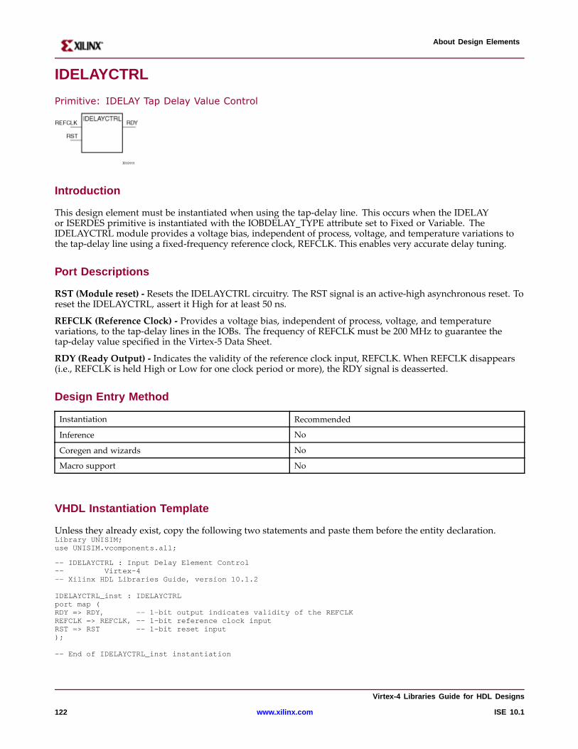
About Design Elements
IDELAYCTRL
Primitive: IDELAY Tap Delay Value Control
Intr oduction
This design element must be instantiated when using the tap-delay line. This occurs when the IDELAYor ISERDES primitive is instantiated with the IOBDELAY_TYPE attribute set to Fixed or Variable. TheIDELAYCTRL module provides a voltage bias, independent of process, voltage, and temperature variations tothe tap-delay line using a fixed-frequency reference clock, REFCLK. This enables very accurate delay tuning.
Por t Descriptions
RST (Module reset) - Resets the IDELAYCTRL circuitry. The RST signal is an active-high asynchronous reset. Toreset the IDELAYCTRL, assert it High for at least 50 ns.
REFCLK (Reference Clock) - Provides a voltage bias, independent of process, voltage, and temperaturevariations, to the tap-delay lines in the IOBs. The frequency of REFCLK must be 200 MHz to guarantee thetap-delay value specified in the Virtex-5 Data Sheet.
RDY (Ready Output) - Indicates the validity of the reference clock input, REFCLK. When REFCLK disappears(i.e., REFCLK is held High or Low for one clock period or more), the RDY signal is deasserted.
Design Entr y Method
Instantiation Recommended
Inference No
Coregen and wizards No
Macro support No
VHDL Instantiation Template
Unless they already exist, copy the following two statements and paste them before the entity declaration.Library UNISIM;use UNISIM.vcomponents.all;
-- IDELAYCTRL : Input Delay Element Control-- Virtex-4-- Xilinx HDL Libraries Guide, version 10.1.2
IDELAYCTRL_inst : IDELAYCTRLport map (RDY => RDY, -- 1-bit output indicates validity of the REFCLKREFCLK => REFCLK, -- 1-bit reference clock inputRST => RST -- 1-bit reset input);
-- End of IDELAYCTRL_inst instantiation
Vir tex-4 Libraries Guide for HDL Designs
122 www.xilinx.com ISE 10.1
About Design Elements
Verilog Instantiation Template
// IDELAYCTRL: Input Delay Control Element (Must be used in conjunction with the IDELAY// when used in FIXED or VARIABLE tap-delay mode)// Virtex-4/5// Xilinx HDL Libraries Guide, version 10.1.2
IDELAYCTRL IDELAYCTRL_inst (.RDY(RDY), // 1-bit ready output.REFCLK(REFCLK), // 1-bit reference clock input.RST(RST) // 1-bit reset input);
// End of IDELAYCTRL_inst instantiation
For More Information
• See the Virtex-4 User Guide.
• See the Virtex-4 Data Sheets.
Vir tex-4 Libraries Guide for HDL Designs
ISE 10.1 www.xilinx.com 123
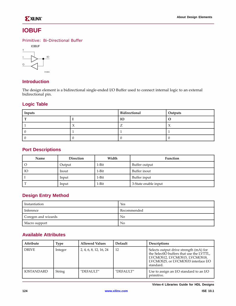
About Design Elements
IOBUF
Primitive: Bi-Directional Buffer
Intr oduction
The design element is a bidirectional single-ended I/O Buffer used to connect internal logic to an externalbidirectional pin.
Logic Table
Inputs Bidirectional Outputs
T I IO O
1 X Z X
0 1 1 1
0 0 0 0
Por t Descriptions
Name Direction Width Function
O Output 1-Bit Buffer output
IO Inout 1-Bit Buffer inout
I Input 1-Bit Buffer input
T Input 1-Bit 3-State enable input
Design Entr y Method
Instantiation Yes
Inference Recommended
Coregen and wizards No
Macro support No
Availab le Attrib utes
Attribute Type Allowed Values Default Descriptions
DRIVE Integer 2, 4, 6, 8, 12, 16, 24 12 Selects output drive strength (mA) forthe SelectIO buffers that use the LVTTL,LVCMOS12, LVCMOS15, LVCMOS18,LVCMOS25, or LVCMOS33 interface I/Ostandard.
IOSTANDARD String "DEFAULT” "DEFAULT” Use to assign an I/O standard to an I/Oprimitive.
Vir tex-4 Libraries Guide for HDL Designs
124 www.xilinx.com ISE 10.1
About Design Elements
Attribute Type Allowed Values Default Descriptions
IBUF_DELAY_VALUE
Binary 0 thru 12 0 Specifies the amount of additional delayto add to the non-registered path out ofthe IOB
IFD_DELAY_VALUE
Binary AUTO, 0 thru 6 AUTO Specifies the amount of additional delayto add to the registered path within theIOB
SLEW Integer "SLOW","FAST” "SLOW” Sets the output rise and fall time.
VHDL Instantiation Template
Unless they already exist, copy the following two statements and paste them before the entity declaration.Library UNISIM;use UNISIM.vcomponents.all;
-- IOBUF: Single-ended Bi-directional Buffer-- All devices-- Xilinx HDL Libraries Guide, version 10.1.2
IOBUF_inst : IOBUFgeneric map (DRIVE => 12,IBUF_DELAY_VALUE => "0", -- Specify the amount of added input delay for buffer, "0"-"16" (Spartan-3E/3A only)IFD_DELAY_VALUE => "AUTO", -- Specify the amount of added delay for input register, "AUTO", "0"-"8" (Spartan-3E/3A only)IOSTANDARD=> "DEFAULT",SLEW=> "SLOW")port map (O => O, -- Buffer outputIO => IO, -- Buffer inout port (connect directly to top-level port)I => I, -- Buffer inputT => T -- 3-state enable input);
-- End of IOBUF_inst instantiation
Verilog Instantiation Template
// IOBUF: Single-ended Bi-directional Buffer// All devices// Xilinx HDL Libraries Guide, version 10.1.2
IOBUF #(.DRIVE(12), // Specify the output drive strength.IBUF_DELAY_VALUE("0"), // Specify the amount of added input delay for the buffer, "0"-"16" (Spartan-3E only).IFD_DELAY_VALUE("AUTO"), // Specify the amount of added delay for input register, "AUTO", "0"-"8" (Spartan-3E only).IOSTANDARD("DEFAULT"), // Specify the I/O standard.SLEW("SLOW") // Specify the output slew rate) IOBUF_inst (.O(O), // Buffer output.IO(IO), // Buffer inout port (connect directly to top-level port).I(I), // Buffer input.T(T) // 3-state enable input);
// End of IOBUF_inst instantiation
For More Information
• See the Virtex-4 User Guide.• See the Virtex-4 Data Sheets.
Vir tex-4 Libraries Guide for HDL Designs
ISE 10.1 www.xilinx.com 125
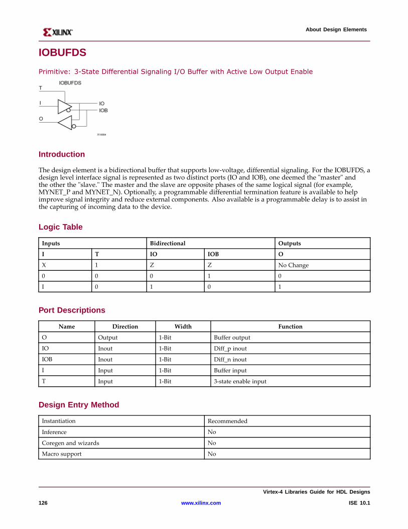
About Design Elements
IOBUFDS
Primitive: 3-State Differential Signaling I/O Buffer with Active Low Output Enable
Intr oduction
The design element is a bidirectional buffer that supports low-voltage, differential signaling. For the IOBUFDS, adesign level interface signal is represented as two distinct ports (IO and IOB), one deemed the "master" andthe other the "slave." The master and the slave are opposite phases of the same logical signal (for example,MYNET_P and MYNET_N). Optionally, a programmable differential termination feature is available to helpimprove signal integrity and reduce external components. Also available is a programmable delay is to assist inthe capturing of incoming data to the device.
Logic Table
Inputs Bidirectional Outputs
I T IO IOB O
X 1 Z Z No Change
0 0 0 1 0
I 0 1 0 1
Por t Descriptions
Name Direction Width Function
O Output 1-Bit Buffer output
IO Inout 1-Bit Diff_p inout
IOB Inout 1-Bit Diff_n inout
I Input 1-Bit Buffer input
T Input 1-Bit 3-state enable input
Design Entr y Method
Instantiation Recommended
Inference No
Coregen and wizards No
Macro support No
Vir tex-4 Libraries Guide for HDL Designs
126 www.xilinx.com ISE 10.1
About Design Elements
Availab le Attrib utes
Attribute Type Allowed Values Default Descriptions
IFD_DELAY_VALUE String "AUTO" or 0 to 6 "AUTO" Specifies the amount of additional delay toadd to the registered path within the IOB.
IOSTANDARD String "DEFAULT” "DEFAULT” Use to assign an I/O standard to an I/Oprimitive.
VHDL Instantiation Template
Unless they already exist, copy the following two statements and paste them before the entity declaration.Library UNISIM;use UNISIM.vcomponents.all;
-- IOBUFDS: Differential Bi-directional Buffer-- Virtex-II/II-Pro, Spartan-3/3E/3A-- Xilinx HDL Libraries Guide, version 10.1.2
IOBUFDS_inst : IOBUFDSgeneric map (IBUF_DELAY_VALUE => "0", -- Specify the amount of added input delay for buffer, "0"-"16" (Spartan-3E/3A only)IFD_DELAY_VALUE => "AUTO", -- Specify the amount of added delay for input register, "AUTO", "0"-"8" (Spartan-3E/3A only)IOSTANDARD=> "DEFAULT")port map (O => O, -- Buffer outputIO => IO, -- Diff_p inout (connect directly to top-level port)IOB => IOB, -- Diff_n inout (connect directly to top-level port)I => I, -- Buffer inputT => T -- 3-state enable input);
-- End of IOBUFDS_inst instantiation
Verilog Instantiation Template
// IOBUFDS: Differential Bi-directional Buffer// Virtex-II/II-Pro/4/5, Spartan-3/3E/3A// Xilinx HDL Libraries Guide, version 10.1.2
IOBUFDS #(.IBUF_DELAY_VALUE("0"), // Specify the amount of added input delay for the buffer, "0"-"16" (Spartan-3E only).IFD_DELAY_VALUE("AUTO"), // Specify the amount of added delay for input register, "AUTO", "0"-"8" (Spartan-3E only).IOSTANDARD("DEFAULT") // Specify the I/O standard) IOBUFDS_inst (.O(O), // Buffer output.IO(IO), // Diff_p inout (connect directly to top-level port).IOB(IOB), // Diff_n inout (connect directly to top-level port).I(I), // Buffer input.T(T) // 3-state enable input);
// End of IOBUFDS_inst instantiation
For More Information
• See the Virtex-4 User Guide.
• See the Virtex-4 Data Sheets.
Vir tex-4 Libraries Guide for HDL Designs
ISE 10.1 www.xilinx.com 127
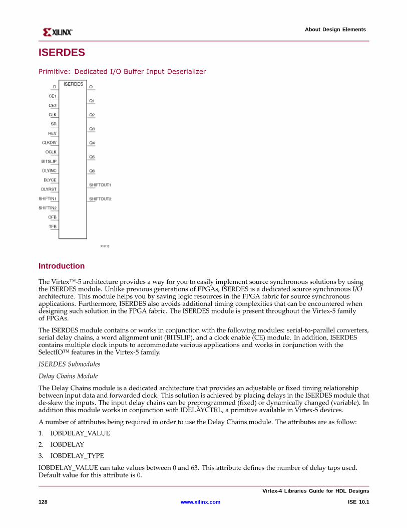
About Design Elements
ISERDES
Primitive: Dedicated I/O Buffer Input Deserializer
Intr oduction
The Virtex™-5 architecture provides a way for you to easily implement source synchronous solutions by usingthe ISERDES module. Unlike previous generations of FPGAs, ISERDES is a dedicated source synchronous I/Oarchitecture. This module helps you by saving logic resources in the FPGA fabric for source synchronousapplications. Furthermore, ISERDES also avoids additional timing complexities that can be encountered whendesigning such solution in the FPGA fabric. The ISERDES module is present throughout the Virtex-5 familyof FPGAs.
The ISERDES module contains or works in conjunction with the following modules: serial-to-parallel converters,serial delay chains, a word alignment unit (BITSLIP), and a clock enable (CE) module. In addition, ISERDEScontains multiple clock inputs to accommodate various applications and works in conjunction with theSelectIO™ features in the Virtex-5 family.
ISERDES Submodules
Delay Chains Module
The Delay Chains module is a dedicated architecture that provides an adjustable or fixed timing relationshipbetween input data and forwarded clock. This solution is achieved by placing delays in the ISERDES module thatde-skew the inputs. The input delay chains can be preprogrammed (fixed) or dynamically changed (variable). Inaddition this module works in conjunction with IDELAYCTRL, a primitive available in Virtex-5 devices.
A number of attributes being required in order to use the Delay Chains module. The attributes are as follow:
1. IOBDELAY_VALUE
2. IOBDELAY
3. IOBDELAY_TYPE
IOBDELAY_VALUE can take values between 0 and 63. This attribute defines the number of delay taps used.Default value for this attribute is 0.
Vir tex-4 Libraries Guide for HDL Designs
128 www.xilinx.com ISE 10.1
About Design Elements
Setting the IOBDELAY attribute to "IBUF," "IFD," and "BOTH" allows the Delay Chains to be used in thecombinatorial output (O output), registered output (Q1-Q6 output), and both respectively. Setting the IOBDELAYattribute to "NONE" bypasses the delay chains module.
The IOBDELAY_TYPE can take three different values: "DEFAULT," "FIXED," or "VARIABLE." The "DEFAULT"allows you to use the 0 hold time value. Using the "FIXED" mode, the delay taps equal to value defined byIOBDELAY_VALUE. In this mode, the value can’t be changed after the device is programmed. In the last mode,"VARIABLE," the delay value is set to an initial value defined by IOBDELAY_VALUE and adjustable after thedevice is programmed.
The Delay Chains module is controlled by DLYRST, DLYCE, and DLYINC pins. Each of the operations performedwith these pins are synchronous to the CLKDIV clock signal. Asserting DLYRST to logic High configures thedelay tap to the value defined in IOBDELAY_VALUE. To increment/decrement the delay tap value, you must useboth DLYCE and DLYINC. For this operation to proceed, the DLYCE must be asserted to logic High. SettingDLYINC to 1 increments and setting DLYINC to 0 decrements the delay tap value.
The following table identifies the Delay Chains Controls:
Operation DLYRST DLYCE DLYINC
Reset to IOBDELAY_VALUE 1 X X
Increment tap value 0 1 1
Decrement tap value 0 1 0
No change 0 0 X
Note All Delay Chains operations are synchronous to CLKDIV.
Serial-to-Parallel Converter
The serial-to-parallel converter in the ISERDES module takes in serial data and convert them into data widthchoices from 2 to 6. Data widths larger than 6 (7,8, and 10) is achievable by cascading two ISERDES modules fordata width expansion. In order to do this, one ISERDES must be set into a MASTER mode, while another isset into SLAVE mode. You need to connect the SHIFTIN of "slave" and SHIFTOUT of "master" ports together.The "slave" uses Q3 to Q6 ports as its output. The serial-to-parallel converter is available for both SDR andDDR modes.
This module is primarily controlled by CLK and CLKDIV clocks. The following table describes the relationshipbetween CLK and CLKDIV for both SDR and DDR mode.
The following table illustrates the CLK/CLKDIV relationship of the serial-to-parallel converter:
SDR Data Width DDR Data Width CLK CLKDIV
2 4 2X X
3 6 3X X
4 8 4X X
5 10 5X X
6 - 6X X
7 - 7X X
8 - 8X X
CE Module
CE Module is essentially a 2:1 parallel-to-serial converter. This module is controlled by CLKDIV clock input andis used to control the clock enable port of the Serial-to-Parallel Converter module.
BITSLIP Module
Vir tex-4 Libraries Guide for HDL Designs
ISE 10.1 www.xilinx.com 129
About Design Elements
The BITSLIP module is a "Barrel Shifter" type function that reorders an output sequence. An output pattern onlychanges whenever the BITSLIP is invoked. The maximum number of BITSLIP reordering is always equal to thenumber of bits in the pattern length minus one (DATA_WIDTH – 1). BITSLIP is supported for both SDR andDDR operations. However, note that the output reordering for SDR and DDR greatly differs.
In order to use the BITSLIP, the attribute "BITSLIP_ENABLE" must be set to "ON." Setting this attribute to "OFF"allows you to bypass the BITSLIP module.
Setting this attribute to "OFF" allows you to bypass the BITSLIP module. The BITSLIP operation is synchronousto the CLKDIV clock input. In order to invoke the BITSLIP module, the BITSLIP port must be asserted Highfor one and only one CLKDIV cycle. After one CLKDIV cycle the BITSLIP port is asserted High, the BITSLIPoperation is completed. For DDR mode, a BITSLIP operation can not be stable until after two CLKDIV cycles.All outputs of the BITSLIP appear in one of the registered output ports (Q1 to Q6) BITSLIP operations aresynchronous to CLKDIV.
Additional Features
Width Expansion
It is possible to use the ISERDES modules to recover data widths larger than 6 bits. In order to use this feature,two ISERDES modules need to be instantiated. Both the ISERDES must be an adjacent master and slave pair.The attribute SERDES_MODE must be set to either "MASTER" or "SLAVE" in order to differentiate the modesof the ISERDES pair. In addition, you must connect the SHIFOUT ports of the MASTER to the SHIFTIN portsof the SLAVE. This feature supports data widths of 7, 8, and 10 for SDR and DDR mode. The table below liststhe data width availability for SDR and DDR mode.
Mode Widths
SDR Data Widths 2,3,4,5,6,7,8
DDR Data Widths 4,6,8,10
Por t Descriptions
Name Type Width Description
O Output 1 Combinatorial Output - This port is an unregisteredoutput of the ISERDES module. It is the unregisteredoutput of the delay chain. In addition, this output portcan also be configured to bypass all the submoduleswithin ISERDES module. This output can be used todrive the BUFIOs.
Q1 – 6 Output 1 (each) Registered Outputs - This port is a registered output ofthe ISERDES module. Using these outputs, you havea selection of the following combination of ISERDESsubmodules path as the inputs:
1. Delay chain to serial-to-parallel converter to bitslipmodule.
2. Delay chain to serial-to-parallel converter.
These ports can be programmed from 2 to 6 bits. In theextended width mode, this port can be expanded up to10 bits.
SHIFTOUT 1 – 2 Output 1 (each) Carry out for data input expansion. Connect toSHIFTIN1/2 of slave.
BITSLIP Input 1 Invokes the ISERDES to perform a BITSLIP operationwhen logic High is given and the BITSLIP module isenabled.
CE 1 – 2 Input 1 (each) Clock enables input that feeds into the CE module.
Vir tex-4 Libraries Guide for HDL Designs
130 www.xilinx.com ISE 10.1
About Design Elements
Name Type Width Description
CLK Input 1 High Speed Forwarded Clock Input - This clock inputis used to drive the Serial to Parallel Converter and theBITSLIP module. The possible source for the CLK port isfrom one of the following clock resources:
1. Eight global clock lines in a clock region
2. Two regional clock lines
3. Six clock capable I/Os (within adjacent clock region)
4. Fabric (through bypass)
CLKDIV Input 1 Divided High Speed Forward Clock Input - This clockinput is used to drive the Serial to Parallel Converter,Delay Chain, the BITSLIP module, and CE module.This clock has to have slower frequency than the clockconnected to the CLK port. The possible source forthe CLKDIV port is from one of the following clockresources:
1. Eight global clock lines in a clock region
2. Two regional clock lines
D Input 1 Serial Input Data From IOB - The D is where all theincoming data enters the ISERDES module. This portworks in conjunction with SelectIO features for Virtex-5architecture to accommodate the desired I/O standards.
DLYCE Input 1 Enable delay chain to be incremented or decremented
DLYINC Input 1 Delay Chain Increment/Decrement Pin - When theDLYCE pin is asserted High, the value at DLYINCpin increments/decrements the delay chain value.Logic High increments the tap value, while logic LOWdecrements the tap value.
DLYRST Input 1 Delay Chain Reset Pin - Resets delay line to programmedvalue of IOBDELAY_VALUE (=Tap Count). If no valueprogrammed, resets delay line to 0 taps.
OCLK Input 1 High Speed Clock for Memory Interfaces Applications- This clock input is used to drive the serial-to-parallelconverter in the ISERDES module. The possible sourcefor the OCLK port is from one of the following clockresources:
1. Eight global clock lines in a clock region
2. Two regional clock lines
3. Six clock capable I/Os (within adjacent clock region)
4. Fabric (through bypass)
This clock is an ideal solution for memory interfaces inwhich strobe signals are required.
REV Input 1 Reverse SR. For internal testing purposes. When SR isused, a second input, REV forces the storage elementinto the opposite state. The reset condition predominatesover the set condition. The REV pin is not supportedin ISERDES.
Vir tex-4 Libraries Guide for HDL Designs
ISE 10.1 www.xilinx.com 131
About Design Elements
Name Type Width Description
SR Input 1 Set/Reset Input - The set/reset pin, SR forces the storageelement into the state specified by the SRVAL attribute,set through your constraints file (UCF). SRVAL = “1”forces a logic 1. SRVAL = “0” forces a logic "0." WhenSR is used, a second input (REV) forces the storageelement into the opposite state. The reset conditionpredominates over the set condition. The SR pin activehigh asynchronous reset for all registers in the ISERDEScomponent.
SHIFTIN 1 – 2 Input 1 (each) Carry input for data input expansion. Connect toSHIFTOUT1/2 of master.
Design Entr y Method
Instantiation Recommended
Inference No
Coregen and wizards No
Macro support No
Availab le Attrib utes
Attribute Type Allowed Values Default Description
BITSLIP_ENABLE Boolean FALSE, TRUE 0 Allows you to enable the bitslipcontroller.
DATA_RATE String "SDR" or "DDR" "DDR” Specify data rate of either allowedvalue.
DATA_WIDTH String If DATA_RATE = "DDR",value is limited to 4, 6, 8,or 10. If DATA_RATE ="SDR", value is limited to2, 3, 4, 5, 6, 7, or 8.
4 Defines the serial-to-parallel converterwidth. This value also depends on theSDR vs. DDR and the Mode of theISERDES.
INTERFACE_TYPE String "MEMORY" or"NETWORKING"
"MEMORY" Determines which ISERDES usemodel is used.
IOBDELAY String "NONE", "IBUF", "IFD","BOTH"
"NONE" Defines where the ISERDES outputsthe Delay Chains.
IOBDELAY_TYPE String "DEFAULT", "FIXED", or"VARIABLE"
"DEFAULT" Defines whether the Delay Chains arein fixed or variable mode.
IOBDELAY_ VALUE Integer 0 to 63 0 Set initial tap delay to an Integer from0 to 63.
NUM_CE Integer 1 or 2 2 Define number or clock enables to anInteger of 1 or 2.
VHDL Instantiation Template
Unless they already exist, copy the following two statements and paste them before the entity declaration.Library UNISIM;use UNISIM.vcomponents.all;
-- ISERDES: Input SERDES-- Virtex-4-- Xilinx HDL Libraries Guide, version 10.1.2
Vir tex-4 Libraries Guide for HDL Designs
132 www.xilinx.com ISE 10.1
About Design Elements
ISERDES_inst : ISERDESgeneric map (BITSLIP_ENABLE => FALSE, -- TRUE/FALSE to enable bitslip controller-- Must be "FALSE" in interface type is "MEMORY"DATA_RATE=> "DDR", -- Specify data rate of "DDR" or "SDR"DATA_WIDTH=> 4, -- Specify data width - For DDR 4,6,8, or 10-- For SDR 2,3,4,5,6,7, or 8INTERFACE_TYPE=> "MEMORY", -- Use model - "MEMORY" or "NETWORKING"IOBDELAY => "NONE", -- Specify outputs where delay chain will be applied-- "NONE", "IBUF", "IFD", or "BOTH"IOBDELAY_TYPE => "DEFAULT", -- Set tap delay "DEFAULT", "FIXED", or "VARIABLE"IOBDELAY_VALUE=> 0, -- Set initial tap delay to an integer from 0 to 63NUM_CE=> 2, -- Define number or clock enables to an integer of 1 or 2SERDES_MODE=> "MASTER") --Set SERDESmode to "MASTER" or "SLAVE"port map (O => O, -- 1-bit outputQ1 => Q1, -- 1-bit outputQ2 => Q2, -- 1-bit outputQ3 => Q3, -- 1-bit outputQ4 => Q4, -- 1-bit outputQ5 => Q5, -- 1-bit outputQ6 => Q6, -- 1-bit outputSHIFTOUT1 => SHIFTOUT1, -- 1-bit outputSHIFTOUT2 => SHIFTOUT2, -- 1-bit outputBITSLIP => BITSLIP, -- 1-bit inputCE1 => CE1, -- 1-bit inputCE2 => CE2, -- 1-bit inputCLK => CLK, -- 1-bit inputCLKDIV => CLKDIV, -- 1-bit inputD => D, -- 1-bit inputDLYCE => DLYCE, -- 1-bit inputDLYINC => DLYINC, -- 1-bit inputDLYRST => DLYRST, -- 1-bit inputOCLK => OCLK, -- 1-bit inputREV => ’0’, -- Must be tied to logic zeroSHIFTIN1 => SHIFTIN1, -- 1-bit inputSHIFTIN2 => SHIFTIN2, -- 1-bit inputSR => SR -- 1-bit input);
-- End of ISERDES_inst instantiation
Verilog Instantiation Template
// ISERDES: Source Synchronous Input Deserializer// Virtex-4// Xilinx HDL Libraries Guide, version 10.1.2
ISERDES #(.BITSLIP_ENABLE("FALSE"), // "TRUE"/"FALSE" to enable bitslip controller// Must be "FALSE" if INTERFACE_TYPEset to "MEMORY".DATA_RATE("DDR"), // Specify data rate of "DDR" or "SDR".DATA_WIDTH(4), // Specify data width - For DDR 4,6,8, or 10// For SDR 2,3,4,5,6,7, or 8.INTERFACE_TYPE("MEMORY"), // Use model - "MEMORY" or "NETWORKING".IOBDELAY("NONE"), // Specify outputs where delay chain will be applied// "NONE", "IBUF", "IFD", or "BOTH".IOBDELAY_TYPE("DEFAULT"), // Set tap delay "DEFAULT", "FIXED", or "VARIABLE".IOBDELAY_VALUE(0), // Set initial tap delay to an integer from 0 to 63.NUM_CE(2), // Define number or clock enables to an integer of 1 or 2.SERDES_MODE("MASTER") // Set SERDESmode to "MASTER" or "SLAVE") ISERDES_inst (.O(O), // 1-bit combinatorial output.Q1(Q1), // 1-bit registered output.Q2(Q2), // 1-bit registered output.Q3(Q3), // 1-bit registered output.Q4(Q4), // 1-bit registered output.Q5(Q5), // 1-bit registered output.Q6(Q6), // 1-bit registered output
Vir tex-4 Libraries Guide for HDL Designs
ISE 10.1 www.xilinx.com 133
About Design Elements
.SHIFTOUT1(SHIFTOUT1), // 1-bit carry output
.SHIFTOUT2(SHIFTOUT2), // 1-bit carry output
.BITSLIP(BITSLIP), // 1-bit Bitslip input
.CE1(CE1), // 1-bit clock enable input
.CE2(CE2), // 1-bit clock enable input
.CLK(CLK), // 1-bit clock input
.CLKDIV(CLKDIV), // 1-bit divided clock input
.D(D), // 1-bit serial data input
.DLYCE(DLYCE), // 1-bit delay chain enable input
.DLYINC(DLYINC), // 1-bit delay increment/decrement input
.DLYRST(DLYRST), // 1-bit delay chain reset input
.OCLK(OCLK), // 1-bit high-speed clock input
.REV(1’b0), // Must be tied to logic zero
.SHIFTIN1(SHIFTIN1), // 1-bit carry input
.SHIFTIN2(SHIFTIN2), // 1-bit carry input
.SR(SR) // 1-bit set/reset input);
// End of ISERDES_inst instantiation
For More Information
• See the Virtex-4 User Guide.
• See the Virtex-4 Data Sheets.
Vir tex-4 Libraries Guide for HDL Designs
134 www.xilinx.com ISE 10.1
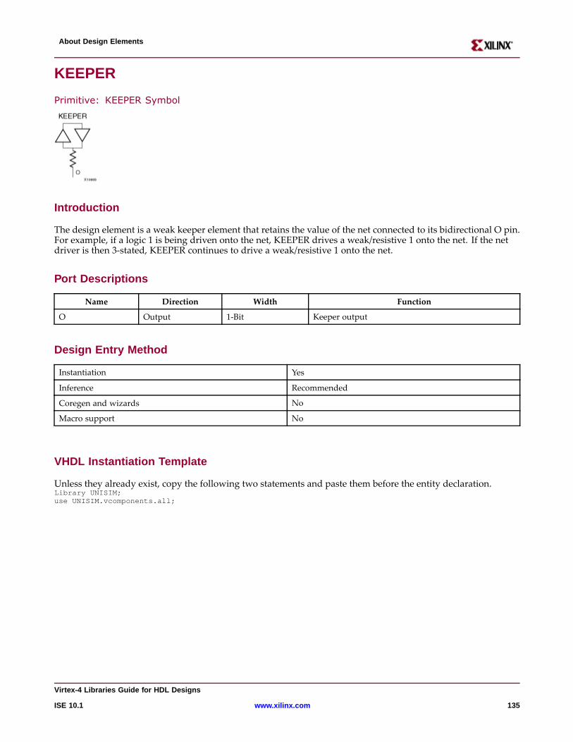
About Design Elements
KEEPER
Primitive: KEEPER Symbol
Intr oduction
The design element is a weak keeper element that retains the value of the net connected to its bidirectional O pin.For example, if a logic 1 is being driven onto the net, KEEPER drives a weak/resistive 1 onto the net. If the netdriver is then 3-stated, KEEPER continues to drive a weak/resistive 1 onto the net.
Por t Descriptions
Name Direction Width Function
O Output 1-Bit Keeper output
Design Entr y Method
Instantiation Yes
Inference Recommended
Coregen and wizards No
Macro support No
VHDL Instantiation Template
Unless they already exist, copy the following two statements and paste them before the entity declaration.Library UNISIM;use UNISIM.vcomponents.all;
Vir tex-4 Libraries Guide for HDL Designs
ISE 10.1 www.xilinx.com 135
About Design Elements
-- KEEPER: I/O Buffer Weak Keeper-- All FPGA, CoolRunner-II-- Xilinx HDL Libraries Guide, version 10.1.2
KEEPER_inst : KEEPERport map (O => O -- Keeper output (connect directly to top-level port));
-- End of KEEPER_inst instantiation
Verilog Instantiation Template
// KEEPER: I/O Buffer Weak Keeper// All FPGA, CoolRunner-II// Xilinx HDL Libraries Guide, version 10.1.2
KEEPERKEEPER_inst (.O(O) // Keeper output (connect directly to top-level port));
// End of KEEPER_inst instantiation
For More Information
• See the Virtex-4 User Guide.
• See the Virtex-4 Data Sheets.
Vir tex-4 Libraries Guide for HDL Designs
136 www.xilinx.com ISE 10.1
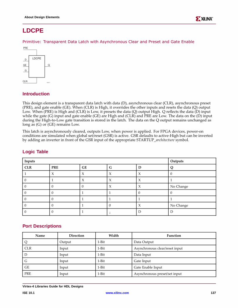
About Design Elements
LDCPE
Primitive: Transparent Data Latch with Asynchronous Clear and Preset and Gate Enable
Intr oduction
This design element is a transparent data latch with data (D), asynchronous clear (CLR), asynchronous preset(PRE), and gate enable (GE). When (CLR) is High, it overrides the other inputs and resets the data (Q) outputLow. When (PRE) is High and (CLR) is Low, it presets the data (Q) output High. Q reflects the data (D) inputwhile the gate (G) input and gate enable (GE) are High and (CLR) and PRE are Low. The data on the (D) inputduring the High-to-Low gate transition is stored in the latch. The data on the Q output remains unchanged aslong as (G) or (GE) remains Low.
This latch is asynchronously cleared, outputs Low, when power is applied. For FPGA devices, power-onconditions are simulated when global set/reset (GSR) is active. GSR defaults to active-High but can be invertedby adding an inverter in front of the GSR input of the appropriate STARTUP_architecture symbol.
Logic Table
Inputs Outputs
CLR PRE GE G D Q
1 X X X X 0
0 1 X X X 1
0 0 0 X X No Change
0 0 1 1 0 0
0 0 1 1 1 1
0 0 1 0 X No Change
0 0 1 ↓ D D
Por t Descriptions
Name Direction Width Function
Q Output 1-Bit Data Output
CLR Input 1-Bit Asynchronous clear/reset input
D Input 1-Bit Data Input
G Input 1-Bit Gate Input
GE Input 1-Bit Gate Enable Input
PRE Input 1-Bit Asynchronous preset/set input
Vir tex-4 Libraries Guide for HDL Designs
ISE 10.1 www.xilinx.com 137
About Design Elements
Design Entr y Method
Instantiation Yes
Inference Recommended
Coregen and wizards No
Macro support No
Availab le Attrib utes
Attribute Type Allowed Values Default Description
INIT Integer 0 or 1 0 Sets the initial value of Q output after configuration.
VHDL Instantiation Template
Unless they already exist, copy the following two statements and paste them before the entity declaration.Library UNISIM;use UNISIM.vcomponents.all;
-- LDCPE: Transparent latch with Asynchronous Reset, Preset and-- Gate Enable.-- All families.-- Xilinx HDL Libraries Guide, version 10.1.2
LDCPE_inst : LDCPEgeneric map (INIT => ’0’) -- Initial value of latch (’0’ or ’1’)port map (Q => Q, -- Data outputCLR => CLR, -- Asynchronous clear/reset inputD => D, -- Data inputG => G, -- Gate inputGE => GE, -- Gate enable inputPRE => PRE -- Asynchronous preset/set input);
-- End of LDCPE_inst instantiation
Verilog Instantiation Template
// LDCPE: Transparent latch with Asynchronous Reset, Preset and// Gate Enable.// All families.// Xilinx HDL Libraries Guide, version 10.1.2
LDCPE #(.INIT(1’b0) // Initial value of latch (1’b0 or 1’b1)) LDCPE_inst (.Q(Q), // Data output.CLR(CLR), // Asynchronous clear/reset input.D(D), // Data input.G(G), // Gate input.GE(GE), // Gate enable input.PRE(PRE) // Asynchronous preset/set input);
// End of LDCPE_inst instantiation
Vir tex-4 Libraries Guide for HDL Designs
138 www.xilinx.com ISE 10.1

About Design Elements
For More Information
• See the Virtex-4 User Guide.
• See the Virtex-4 Data Sheets.
Vir tex-4 Libraries Guide for HDL Designs
ISE 10.1 www.xilinx.com 139
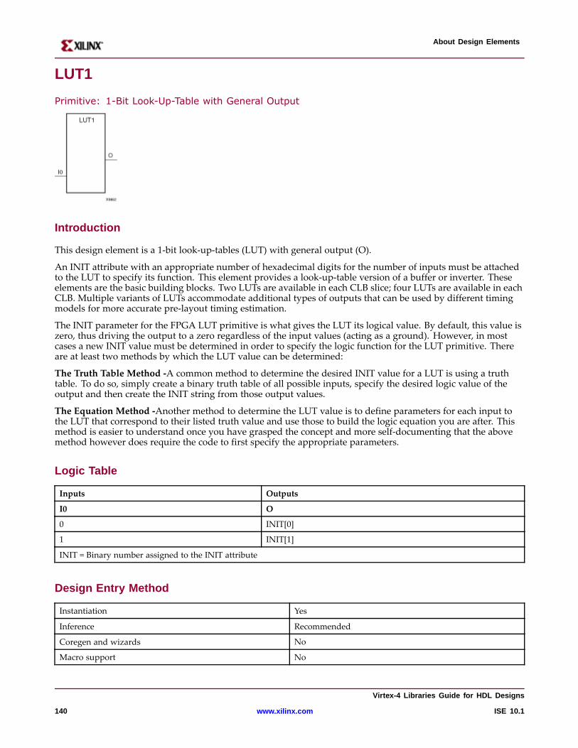
About Design Elements
LUT1
Primitive: 1-Bit Look-Up-Table with General Output
Intr oduction
This design element is a 1-bit look-up-tables (LUT) with general output (O).
An INIT attribute with an appropriate number of hexadecimal digits for the number of inputs must be attachedto the LUT to specify its function. This element provides a look-up-table version of a buffer or inverter. Theseelements are the basic building blocks. Two LUTs are available in each CLB slice; four LUTs are available in eachCLB. Multiple variants of LUTs accommodate additional types of outputs that can be used by different timingmodels for more accurate pre-layout timing estimation.
The INIT parameter for the FPGA LUT primitive is what gives the LUT its logical value. By default, this value iszero, thus driving the output to a zero regardless of the input values (acting as a ground). However, in mostcases a new INIT value must be determined in order to specify the logic function for the LUT primitive. Thereare at least two methods by which the LUT value can be determined:
The Truth Table Method -A common method to determine the desired INIT value for a LUT is using a truthtable. To do so, simply create a binary truth table of all possible inputs, specify the desired logic value of theoutput and then create the INIT string from those output values.
The Equation Method -Another method to determine the LUT value is to define parameters for each input tothe LUT that correspond to their listed truth value and use those to build the logic equation you are after. Thismethod is easier to understand once you have grasped the concept and more self-documenting that the abovemethod however does require the code to first specify the appropriate parameters.
Logic Table
Inputs Outputs
I0 O
0 INIT[0]
1 INIT[1]
INIT = Binary number assigned to the INIT attribute
Design Entr y Method
Instantiation Yes
Inference Recommended
Coregen and wizards No
Macro support No
Vir tex-4 Libraries Guide for HDL Designs
140 www.xilinx.com ISE 10.1
About Design Elements
Availab le Attrib utes
Attribute Type Allowed Values Default Description
INIT Hexadecimal Any 2-Bit Value All zeros Initializes look-up tables.
VHDL Instantiation Template
Unless they already exist, copy the following two statements and paste them before the entity declaration.Library UNISIM;use UNISIM.vcomponents.all;
-- LUT1: 1-input Look-Up Table with general output-- Xilinx HDL Libraries Guide, version 10.1.2
LUT1_inst : LUT1generic map (INIT => "00")port map (O => O, -- LUT general outputI0 => I0 -- LUT input);
-- End of LUT1_inst instantiation
Verilog Instantiation Template
// LUT1: 1-input Look-Up Table with general output// For use with all FPGAs.// Xilinx HDL Libraries Guide, version 10.1.2
LUT1 #(.INIT(2’b00) // Specify LUT Contents) LUT1_inst (.O(O), // LUT general output.I0(I0) // LUT input);
// End of LUT1_inst instantiation
For More Information
• See the Virtex-4 User Guide.
• See the Virtex-4 Data Sheets.
Vir tex-4 Libraries Guide for HDL Designs
ISE 10.1 www.xilinx.com 141
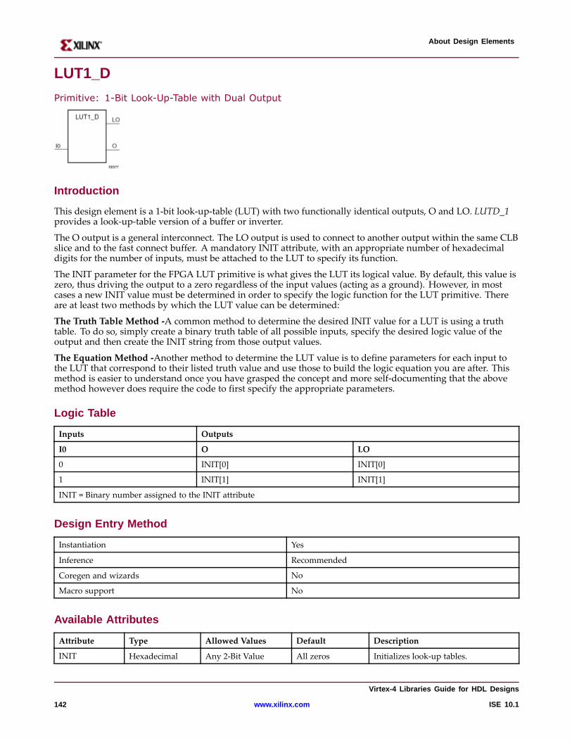
About Design Elements
LUT1_D
Primitive: 1-Bit Look-Up-Table with Dual Output
Intr oduction
This design element is a 1-bit look-up-table (LUT) with two functionally identical outputs, O and LO. LUTD_1provides a look-up-table version of a buffer or inverter.
The O output is a general interconnect. The LO output is used to connect to another output within the same CLBslice and to the fast connect buffer. A mandatory INIT attribute, with an appropriate number of hexadecimaldigits for the number of inputs, must be attached to the LUT to specify its function.
The INIT parameter for the FPGA LUT primitive is what gives the LUT its logical value. By default, this value iszero, thus driving the output to a zero regardless of the input values (acting as a ground). However, in mostcases a new INIT value must be determined in order to specify the logic function for the LUT primitive. Thereare at least two methods by which the LUT value can be determined:
The Truth Table Method -A common method to determine the desired INIT value for a LUT is using a truthtable. To do so, simply create a binary truth table of all possible inputs, specify the desired logic value of theoutput and then create the INIT string from those output values.
The Equation Method -Another method to determine the LUT value is to define parameters for each input tothe LUT that correspond to their listed truth value and use those to build the logic equation you are after. Thismethod is easier to understand once you have grasped the concept and more self-documenting that the abovemethod however does require the code to first specify the appropriate parameters.
Logic Table
Inputs Outputs
I0 O LO
0 INIT[0] INIT[0]
1 INIT[1] INIT[1]
INIT = Binary number assigned to the INIT attribute
Design Entr y Method
Instantiation Yes
Inference Recommended
Coregen and wizards No
Macro support No
Availab le Attrib utes
Attribute Type Allowed Values Default Description
INIT Hexadecimal Any 2-Bit Value All zeros Initializes look-up tables.
Vir tex-4 Libraries Guide for HDL Designs
142 www.xilinx.com ISE 10.1
About Design Elements
VHDL Instantiation Template
Unless they already exist, copy the following two statements and paste them before the entity declaration.Library UNISIM;use UNISIM.vcomponents.all;
-- LUT1_D: 1-input Look-Up Table with general and local outputs-- Xilinx HDL Libraries Guide, version 10.1.2
LUT1_D_inst : LUT1_Dgeneric map (INIT => "00")port map (LO => LO, -- LUT local outputO => O, -- LUT general outputI0 => I0 -- LUT input);
-- End of LUT1_D_inst instantiation
Verilog Instantiation Template
// LUT1_D: 1-input Look-Up Table with general and local outputs// For use with all FPGAs.// Xilinx HDL Libraries Guide, version 10.1.2
LUT1_D #(.INIT(2’b00) // Specify LUT Contents) LUT1_D_inst (.LO(LO), // LUT local output.O(O), // LUT general output.I0(I0) // LUT input);
// End of LUT1_D_inst instantiation
Vir tex-4 Libraries Guide for HDL Designs
ISE 10.1 www.xilinx.com 143

About Design Elements
For More Information
• See the Virtex-4 User Guide.
• See the Virtex-4 Data Sheets.
Vir tex-4 Libraries Guide for HDL Designs
144 www.xilinx.com ISE 10.1
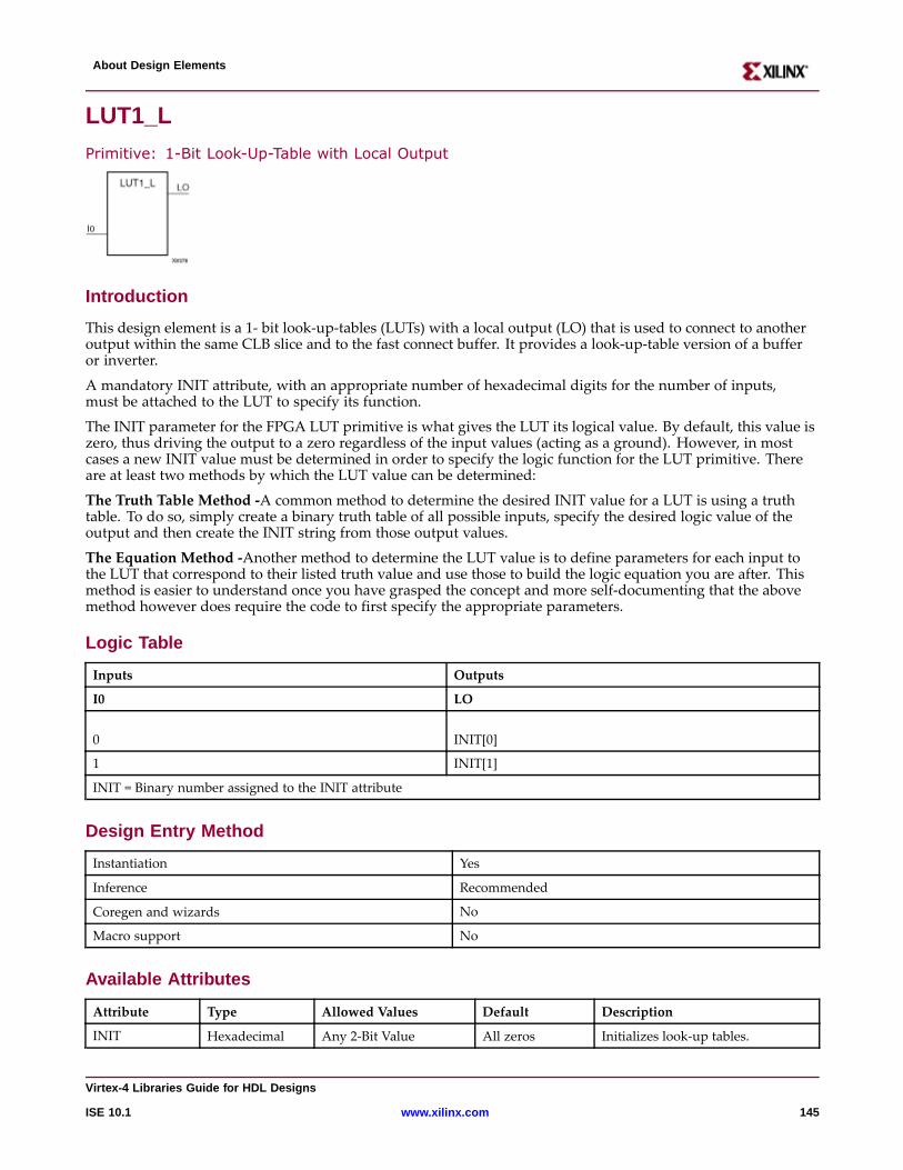
About Design Elements
LUT1_L
Primitive: 1-Bit Look-Up-Table with Local Output
Intr oduction
This design element is a 1- bit look-up-tables (LUTs) with a local output (LO) that is used to connect to anotheroutput within the same CLB slice and to the fast connect buffer. It provides a look-up-table version of a bufferor inverter.
A mandatory INIT attribute, with an appropriate number of hexadecimal digits for the number of inputs,must be attached to the LUT to specify its function.
The INIT parameter for the FPGA LUT primitive is what gives the LUT its logical value. By default, this value iszero, thus driving the output to a zero regardless of the input values (acting as a ground). However, in mostcases a new INIT value must be determined in order to specify the logic function for the LUT primitive. Thereare at least two methods by which the LUT value can be determined:
The Truth Table Method -A common method to determine the desired INIT value for a LUT is using a truthtable. To do so, simply create a binary truth table of all possible inputs, specify the desired logic value of theoutput and then create the INIT string from those output values.
The Equation Method -Another method to determine the LUT value is to define parameters for each input tothe LUT that correspond to their listed truth value and use those to build the logic equation you are after. Thismethod is easier to understand once you have grasped the concept and more self-documenting that the abovemethod however does require the code to first specify the appropriate parameters.
Logic Table
Inputs Outputs
I0 LO
0 INIT[0]
1 INIT[1]
INIT = Binary number assigned to the INIT attribute
Design Entr y Method
Instantiation Yes
Inference Recommended
Coregen and wizards No
Macro support No
Availab le Attrib utes
Attribute Type Allowed Values Default Description
INIT Hexadecimal Any 2-Bit Value All zeros Initializes look-up tables.
Vir tex-4 Libraries Guide for HDL Designs
ISE 10.1 www.xilinx.com 145
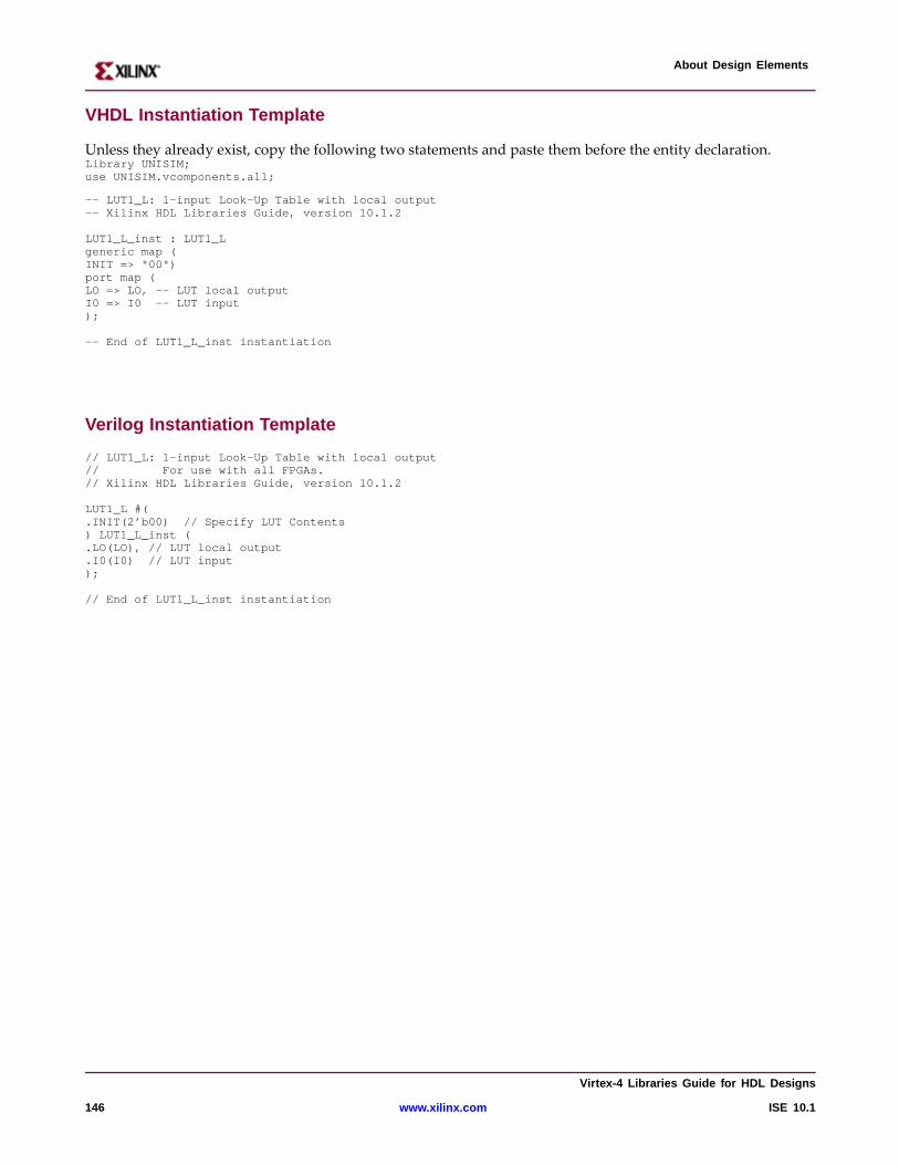
About Design Elements
VHDL Instantiation Template
Unless they already exist, copy the following two statements and paste them before the entity declaration.Library UNISIM;use UNISIM.vcomponents.all;
-- LUT1_L: 1-input Look-Up Table with local output-- Xilinx HDL Libraries Guide, version 10.1.2
LUT1_L_inst : LUT1_Lgeneric map (INIT => "00")port map (LO => LO, -- LUT local outputI0 => I0 -- LUT input);
-- End of LUT1_L_inst instantiation
Verilog Instantiation Template
// LUT1_L: 1-input Look-Up Table with local output// For use with all FPGAs.// Xilinx HDL Libraries Guide, version 10.1.2
LUT1_L #(.INIT(2’b00) // Specify LUT Contents) LUT1_L_inst (.LO(LO), // LUT local output.I0(I0) // LUT input);
// End of LUT1_L_inst instantiation
Vir tex-4 Libraries Guide for HDL Designs
146 www.xilinx.com ISE 10.1

About Design Elements
For More Information
• See the Virtex-4 User Guide.
• See the Virtex-4 Data Sheets.
Vir tex-4 Libraries Guide for HDL Designs
ISE 10.1 www.xilinx.com 147
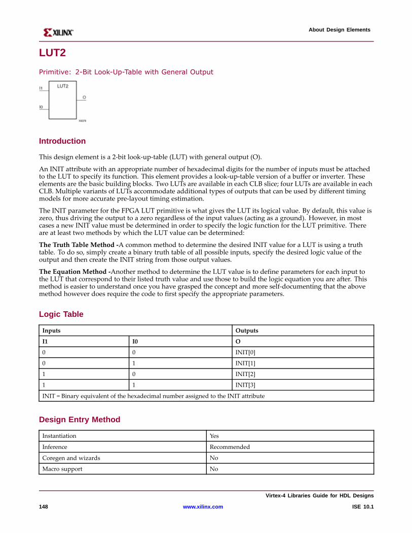
About Design Elements
LUT2
Primitive: 2-Bit Look-Up-Table with General Output
Intr oduction
This design element is a 2-bit look-up-table (LUT) with general output (O).
An INIT attribute with an appropriate number of hexadecimal digits for the number of inputs must be attachedto the LUT to specify its function. This element provides a look-up-table version of a buffer or inverter. Theseelements are the basic building blocks. Two LUTs are available in each CLB slice; four LUTs are available in eachCLB. Multiple variants of LUTs accommodate additional types of outputs that can be used by different timingmodels for more accurate pre-layout timing estimation.
The INIT parameter for the FPGA LUT primitive is what gives the LUT its logical value. By default, this value iszero, thus driving the output to a zero regardless of the input values (acting as a ground). However, in mostcases a new INIT value must be determined in order to specify the logic function for the LUT primitive. Thereare at least two methods by which the LUT value can be determined:
The Truth Table Method -A common method to determine the desired INIT value for a LUT is using a truthtable. To do so, simply create a binary truth table of all possible inputs, specify the desired logic value of theoutput and then create the INIT string from those output values.
The Equation Method -Another method to determine the LUT value is to define parameters for each input tothe LUT that correspond to their listed truth value and use those to build the logic equation you are after. Thismethod is easier to understand once you have grasped the concept and more self-documenting that the abovemethod however does require the code to first specify the appropriate parameters.
Logic Table
Inputs Outputs
I1 I0 O
0 0 INIT[0]
0 1 INIT[1]
1 0 INIT[2]
1 1 INIT[3]
INIT = Binary equivalent of the hexadecimal number assigned to the INIT attribute
Design Entr y Method
Instantiation Yes
Inference Recommended
Coregen and wizards No
Macro support No
Vir tex-4 Libraries Guide for HDL Designs
148 www.xilinx.com ISE 10.1
About Design Elements
Availab le Attrib utes
Attribute Type Allowed Values Default Description
INIT Hexadecimal Any 4-Bit Value All zeros Initializes look-up tables.
VHDL Instantiation Template
Unless they already exist, copy the following two statements and paste them before the entity declaration.Library UNISIM;use UNISIM.vcomponents.all;
-- LUT2: 2-input Look-Up Table with general output-- Xilinx HDL Libraries Guide, version 10.1.2
LUT2_inst : LUT2generic map (INIT => X"0")port map (O => O, -- LUT general outputI0 => I0, -- LUT inputI1 => I1 -- LUT input);
-- End of LUT2_inst instantiation
Verilog Instantiation Template
// LUT2: 2-input Look-Up Table with general output// For use with all FPGAs.// Xilinx HDL Libraries Guide, version 10.1.2
LUT2 #(.INIT(4’h0) // Specify LUT Contents) LUT2_inst (.O(O), // LUT general output.I0(I0), // LUT input.I1(I1) // LUT input);
// End of LUT2_inst instantiation
For More Information
• See the Virtex-4 User Guide.
• See the Virtex-4 Data Sheets.
Vir tex-4 Libraries Guide for HDL Designs
ISE 10.1 www.xilinx.com 149
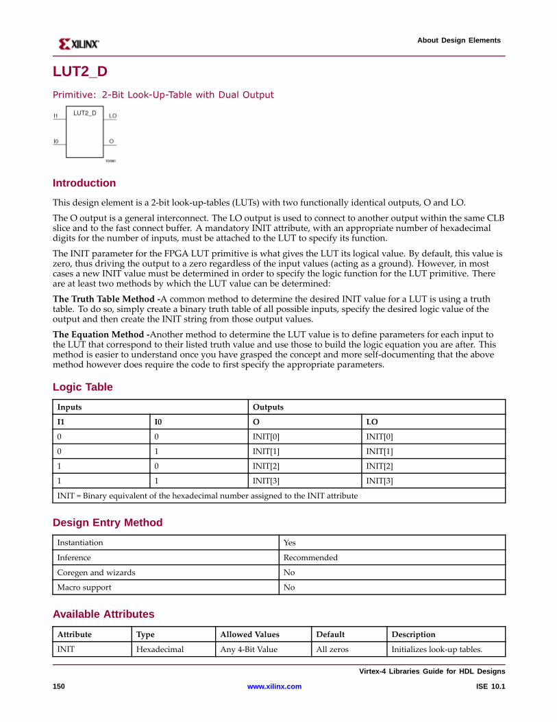
About Design Elements
LUT2_D
Primitive: 2-Bit Look-Up-Table with Dual Output
Intr oduction
This design element is a 2-bit look-up-tables (LUTs) with two functionally identical outputs, O and LO.
The O output is a general interconnect. The LO output is used to connect to another output within the same CLBslice and to the fast connect buffer. A mandatory INIT attribute, with an appropriate number of hexadecimaldigits for the number of inputs, must be attached to the LUT to specify its function.
The INIT parameter for the FPGA LUT primitive is what gives the LUT its logical value. By default, this value iszero, thus driving the output to a zero regardless of the input values (acting as a ground). However, in mostcases a new INIT value must be determined in order to specify the logic function for the LUT primitive. Thereare at least two methods by which the LUT value can be determined:
The Truth Table Method -A common method to determine the desired INIT value for a LUT is using a truthtable. To do so, simply create a binary truth table of all possible inputs, specify the desired logic value of theoutput and then create the INIT string from those output values.
The Equation Method -Another method to determine the LUT value is to define parameters for each input tothe LUT that correspond to their listed truth value and use those to build the logic equation you are after. Thismethod is easier to understand once you have grasped the concept and more self-documenting that the abovemethod however does require the code to first specify the appropriate parameters.
Logic Table
Inputs Outputs
I1 I0 O LO
0 0 INIT[0] INIT[0]
0 1 INIT[1] INIT[1]
1 0 INIT[2] INIT[2]
1 1 INIT[3] INIT[3]
INIT = Binary equivalent of the hexadecimal number assigned to the INIT attribute
Design Entr y Method
Instantiation Yes
Inference Recommended
Coregen and wizards No
Macro support No
Availab le Attrib utes
Attribute Type Allowed Values Default Description
INIT Hexadecimal Any 4-Bit Value All zeros Initializes look-up tables.
Vir tex-4 Libraries Guide for HDL Designs
150 www.xilinx.com ISE 10.1
About Design Elements
VHDL Instantiation Template
Unless they already exist, copy the following two statements and paste them before the entity declaration.Library UNISIM;use UNISIM.vcomponents.all;
-- LUT2_D: 2-input Look-Up Table with general and local outputs-- Xilinx HDL Libraries Guide, version 10.1.2
LUT2_D_inst : LUT2_Dgeneric map (INIT => X"0")port map (LO => LO, -- LUT local outputO => O, -- LUT general outputI0 => I0, -- LUT inputI1 => I1 -- LUT input);
-- End of LUT2_D_inst instantiation
Verilog Instantiation Template
// LUT2_D: 2-input Look-Up Table with general and local outputs// For use with all FPGAs.// Xilinx HDL Libraries Guide, version 10.1.2
LUT2_D #(.INIT(4’h0) // Specify LUT Contents) LUT2_D_inst (.LO(LO), // LUT local output.O(O), // LUT general output.I0(I0), // LUT input.I1(I1) // LUT input);
// End of LUT2_L_inst instantiation
Vir tex-4 Libraries Guide for HDL Designs
ISE 10.1 www.xilinx.com 151
About Design Elements
For More Information
• See the Virtex-4 User Guide.
• See the Virtex-4 Data Sheets.
Vir tex-4 Libraries Guide for HDL Designs
152 www.xilinx.com ISE 10.1
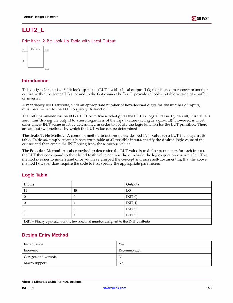
About Design Elements
LUT2_L
Primitive: 2-Bit Look-Up-Table with Local Output
Intr oduction
This design element is a 2- bit look-up-tables (LUTs) with a local output (LO) that is used to connect to anotheroutput within the same CLB slice and to the fast connect buffer. It provides a look-up-table version of a bufferor inverter.
A mandatory INIT attribute, with an appropriate number of hexadecimal digits for the number of inputs,must be attached to the LUT to specify its function.
The INIT parameter for the FPGA LUT primitive is what gives the LUT its logical value. By default, this value iszero, thus driving the output to a zero regardless of the input values (acting as a ground). However, in mostcases a new INIT value must be determined in order to specify the logic function for the LUT primitive. Thereare at least two methods by which the LUT value can be determined:
The Truth Table Method -A common method to determine the desired INIT value for a LUT is using a truthtable. To do so, simply create a binary truth table of all possible inputs, specify the desired logic value of theoutput and then create the INIT string from those output values.
The Equation Method -Another method to determine the LUT value is to define parameters for each input tothe LUT that correspond to their listed truth value and use those to build the logic equation you are after. Thismethod is easier to understand once you have grasped the concept and more self-documenting that the abovemethod however does require the code to first specify the appropriate parameters.
Logic Table
Inputs Outputs
I1 I0 LO
0 0 INIT[0]
0 1 INIT[1]
1 0 INIT[2]
1 1 INIT[3]
INIT = Binary equivalent of the hexadecimal number assigned to the INIT attribute
Design Entr y Method
Instantiation Yes
Inference Recommended
Coregen and wizards No
Macro support No
Vir tex-4 Libraries Guide for HDL Designs
ISE 10.1 www.xilinx.com 153
About Design Elements
Availab le Attrib utes
Attribute Type Allowed Values Default Description
INIT Hexadecimal Any 4-Bit Value All zeros Initializes look-up tables.
VHDL Instantiation Template
Unless they already exist, copy the following two statements and paste them before the entity declaration.Library UNISIM;use UNISIM.vcomponents.all;
-- LUT2_L: 2-input Look-Up Table with local output-- Xilinx HDL Libraries Guide, version 10.1.2
LUT2_L_inst : LUT2_Lgeneric map (INIT => X"0")port map (LO => LO, -- LUT local outputI0 => I0, -- LUT inputI1 => I1 -- LUT input);
-- End of LUT2_L_inst instantiation
Verilog Instantiation Template
// LUT2_L: 2-input Look-Up Table with local output// For use with all FPGAs.// Xilinx HDL Libraries Guide, version 10.1.2
LUT2_L #(.INIT(4’h0) // Specify LUT Contents) LUT2_L_inst (.LO(LO), // LUT local output.I0(I0), // LUT input.I1(I1) // LUT input);
// End of LUT2_L_inst instantiation
For More Information
• See the Virtex-4 User Guide.
• See the Virtex-4 Data Sheets.
Vir tex-4 Libraries Guide for HDL Designs
154 www.xilinx.com ISE 10.1
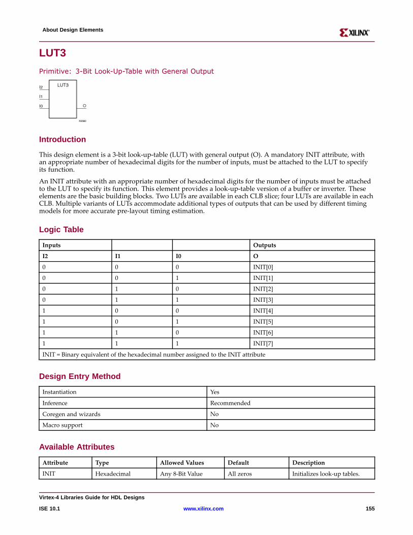
About Design Elements
LUT3
Primitive: 3-Bit Look-Up-Table with General Output
Intr oduction
This design element is a 3-bit look-up-table (LUT) with general output (O). A mandatory INIT attribute, withan appropriate number of hexadecimal digits for the number of inputs, must be attached to the LUT to specifyits function.
An INIT attribute with an appropriate number of hexadecimal digits for the number of inputs must be attachedto the LUT to specify its function. This element provides a look-up-table version of a buffer or inverter. Theseelements are the basic building blocks. Two LUTs are available in each CLB slice; four LUTs are available in eachCLB. Multiple variants of LUTs accommodate additional types of outputs that can be used by different timingmodels for more accurate pre-layout timing estimation.
Logic Table
Inputs Outputs
I2 I1 I0 O
0 0 0 INIT[0]
0 0 1 INIT[1]
0 1 0 INIT[2]
0 1 1 INIT[3]
1 0 0 INIT[4]
1 0 1 INIT[5]
1 1 0 INIT[6]
1 1 1 INIT[7]
INIT = Binary equivalent of the hexadecimal number assigned to the INIT attribute
Design Entr y Method
Instantiation Yes
Inference Recommended
Coregen and wizards No
Macro support No
Availab le Attrib utes
Attribute Type Allowed Values Default Description
INIT Hexadecimal Any 8-Bit Value All zeros Initializes look-up tables.
Vir tex-4 Libraries Guide for HDL Designs
ISE 10.1 www.xilinx.com 155
About Design Elements
VHDL Instantiation Template
Unless they already exist, copy the following two statements and paste them before the entity declaration.Library UNISIM;use UNISIM.vcomponents.all;
-- LUT3: 3-input Look-Up Table with general output-- Xilinx HDL Libraries Guide, version 10.1.2
LUT3_inst : LUT3generic map (INIT => X"00")port map (O => O, -- LUT general outputI0 => I0, -- LUT inputI1 => I1, -- LUT inputI2 => I2 -- LUT input);
-- End of LUT3_inst instantiation
Verilog Instantiation Template
// LUT3: 3-input Look-Up Table with general output// For use with all FPGAs.// Xilinx HDL Libraries Guide, version 10.1.2
LUT3 #(.INIT(8’h00) // Specify LUT Contents) LUT3_inst (.O(O), // LUT general output.I0(I0), // LUT input.I1(I1), // LUT input.I2(I2) // LUT input);
// End of LUT3_inst instantiation
For More Information
• See the Virtex-4 User Guide.
• See the Virtex-4 Data Sheets.
Vir tex-4 Libraries Guide for HDL Designs
156 www.xilinx.com ISE 10.1
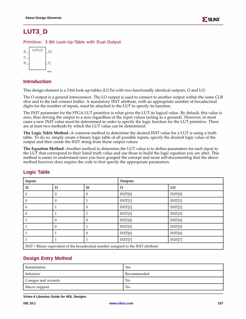
About Design Elements
LUT3_D
Primitive: 3-Bit Look-Up-Table with Dual Output
Intr oduction
This design element is a 3-bit look-up-tables (LUTs) with two functionally identical outputs, O and LO.
The O output is a general interconnect. The LO output is used to connect to another output within the same CLBslice and to the fast connect buffer. A mandatory INIT attribute, with an appropriate number of hexadecimaldigits for the number of inputs, must be attached to the LUT to specify its function.
The INIT parameter for the FPGA LUT primitive is what gives the LUT its logical value. By default, this value iszero, thus driving the output to a zero regardless of the input values (acting as a ground). However, in mostcases a new INIT value must be determined in order to specify the logic function for the LUT primitive. Thereare at least two methods by which the LUT value can be determined:
The Logic Table Method -A common method to determine the desired INIT value for a LUT is using a truthtable. To do so, simply create a binary logic table of all possible inputs, specify the desired logic value of theoutput and then create the INIT string from those output values.
The Equation Method -Another method to determine the LUT value is to define parameters for each input tothe LUT that correspond to their listed truth value and use those to build the logic equation you are after. Thismethod is easier to understand once you have grasped the concept and more self-documenting that the abovemethod however does require the code to first specify the appropriate parameters.
Logic Table
Inputs Outputs
I2 I1 I0 O LO
0 0 0 INIT[0] INIT[0]
0 0 1 INIT[1] INIT[1]
0 1 0 INIT[2] INIT[2]
0 1 1 INIT[3] INIT[3]
1 0 0 INIT[4] INIT[4]
1 0 1 INIT[5] INIT[5]
1 1 0 INIT[6] INIT[6]
1 1 1 INIT[7] INIT[7]
INIT = Binary equivalent of the hexadecimal number assigned to the INIT attribute
Design Entr y Method
Instantiation Yes
Inference Recommended
Coregen and wizards No
Macro support No
Vir tex-4 Libraries Guide for HDL Designs
ISE 10.1 www.xilinx.com 157
About Design Elements
Availab le Attrib utes
Attribute Type Allowed Values Default Description
INIT Hexadecimal Any 8-Bit Value All zeros Initializes look-up tables.
VHDL Instantiation Template
Unless they already exist, copy the following two statements and paste them before the entity declaration.Library UNISIM;use UNISIM.vcomponents.all;
-- LUT3_D: 3-input Look-Up Table with general and local outputs-- Xilinx HDL Libraries Guide, version 10.1.2
LUT3_D_inst : LUT3_Dgeneric map (INIT => X"00")port map (LO => LO, -- LUT local outputO => O, -- LUT general outputI0 => I0, -- LUT inputI1 => I1, -- LUT inputI2 => I2 -- LUT input);
-- End of LUT3_D_inst instantiation
Verilog Instantiation Template
// LUT3_D: 3-input Look-Up Table with general and local outputs// For use with all FPGAs.// Xilinx HDL Libraries Guide, version 10.1.2
LUT3_D #(.INIT(8’h00) // Specify LUT Contents) LUT3_D_inst (.LO(LO), // LUT local output.O(O), // LUT general output.I0(I0), // LUT input.I1(I1), // LUT input.I2(I2) // LUT input);
// End of LUT3_D_inst instantiation
For More Information
• See the Virtex-4 User Guide.
• See the Virtex-4 Data Sheets.
Vir tex-4 Libraries Guide for HDL Designs
158 www.xilinx.com ISE 10.1
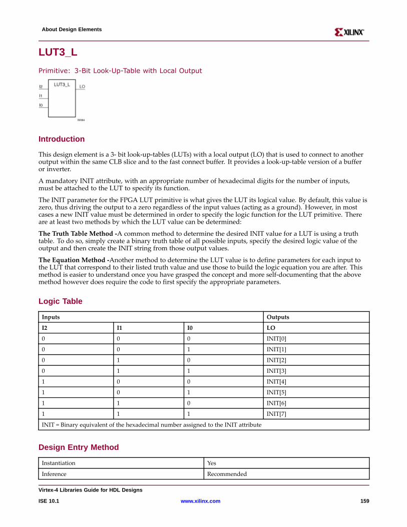
About Design Elements
LUT3_L
Primitive: 3-Bit Look-Up-Table with Local Output
Intr oduction
This design element is a 3- bit look-up-tables (LUTs) with a local output (LO) that is used to connect to anotheroutput within the same CLB slice and to the fast connect buffer. It provides a look-up-table version of a bufferor inverter.
A mandatory INIT attribute, with an appropriate number of hexadecimal digits for the number of inputs,must be attached to the LUT to specify its function.
The INIT parameter for the FPGA LUT primitive is what gives the LUT its logical value. By default, this value iszero, thus driving the output to a zero regardless of the input values (acting as a ground). However, in mostcases a new INIT value must be determined in order to specify the logic function for the LUT primitive. Thereare at least two methods by which the LUT value can be determined:
The Truth Table Method -A common method to determine the desired INIT value for a LUT is using a truthtable. To do so, simply create a binary truth table of all possible inputs, specify the desired logic value of theoutput and then create the INIT string from those output values.
The Equation Method -Another method to determine the LUT value is to define parameters for each input tothe LUT that correspond to their listed truth value and use those to build the logic equation you are after. Thismethod is easier to understand once you have grasped the concept and more self-documenting that the abovemethod however does require the code to first specify the appropriate parameters.
Logic Table
Inputs Outputs
I2 I1 I0 LO
0 0 0 INIT[0]
0 0 1 INIT[1]
0 1 0 INIT[2]
0 1 1 INIT[3]
1 0 0 INIT[4]
1 0 1 INIT[5]
1 1 0 INIT[6]
1 1 1 INIT[7]
INIT = Binary equivalent of the hexadecimal number assigned to the INIT attribute
Design Entr y Method
Instantiation Yes
Inference Recommended
Vir tex-4 Libraries Guide for HDL Designs
ISE 10.1 www.xilinx.com 159
About Design Elements
Coregen and wizards No
Macro support No
Availab le Attrib utes
Attribute Type Allowed Values Default Description
INIT Hexadecimal Any 8-Bit Value All zeros Initializes look-up tables.
VHDL Instantiation Template
Unless they already exist, copy the following two statements and paste them before the entity declaration.Library UNISIM;use UNISIM.vcomponents.all;
-- LUT3_L: 3-input Look-Up Table with local output-- Xilinx HDL Libraries Guide, version 10.1.2
LUT3_L_inst : LUT3_Lgeneric map (INIT => X"00")port map (LO => LO, -- LUT local outputI0 => I0, -- LUT inputI1 => I1, -- LUT inputI2 => I2 -- LUT input);
-- End of LUT3_L_inst instantiation
Verilog Instantiation Template
// LUT3_L: 3-input Look-Up Table with local output// For use with all FPGAs.// Xilinx HDL Libraries Guide, version 10.1.2
LUT3_L #(.INIT(8’h00) // Specify LUT Contents) LUT3_L_inst (.LO(LO), // LUT local output.I0(I0), // LUT input.I1(I1), // LUT input.I2(I2) // LUT input);
// End of LUT3_L_inst instantiation
For More Information
• See the Virtex-4 User Guide.
• See the Virtex-4 Data Sheets.
Vir tex-4 Libraries Guide for HDL Designs
160 www.xilinx.com ISE 10.1

About Design Elements
LUT4
Primitive: 4-Bit Look-Up-Table with General Output
Intr oduction
This design element is a 4-bit look-up-tables (LUT) with general output (O).
An INIT attribute with an appropriate number of hexadecimal digits for the number of inputs must be attachedto the LUT to specify its function. This element provides a look-up-table version of a buffer or inverter. Theseelements are the basic building blocks. Two LUTs are available in each CLB slice; four LUTs are available in eachCLB. Multiple variants of LUTs accommodate additional types of outputs that can be used by different timingmodels for more accurate pre-layout timing estimation.
The INIT parameter for the FPGA LUT primitive is what gives the LUT its logical value. By default, this value iszero, thus driving the output to a zero regardless of the input values (acting as a ground). However, in mostcases a new INIT value must be determined in order to specify the logic function for the LUT primitive. Thereare at least two methods by which the LUT value can be determined:
The Truth Table Method -A common method to determine the desired INIT value for a LUT is using a truthtable. To do so, simply create a binary truth table of all possible inputs, specify the desired logic value of theoutput and then create the INIT string from those output values.
The Equation Method -Another method to determine the LUT value is to define parameters for each input tothe LUT that correspond to their listed truth value and use those to build the logic equation you are after. Thismethod is easier to understand once you have grasped the concept and more self-documenting that the abovemethod however does require the code to first specify the appropriate parameters.
Logic Table
Inputs Outputs
I3 I2 I1 I0 O
0 0 0 0 INIT[0]
0 0 0 1 INIT[1]
0 0 1 0 INIT[2]
0 0 1 1 INIT[3]
0 1 0 0 INIT[4]
0 1 0 1 INIT[5]
0 1 1 0 INIT[6]
0 1 1 1 INIT[7]
1 0 0 0 INIT[8]
1 0 0 1 INIT[9]
1 0 1 0 INIT[10]
1 0 1 1 INIT[11]
1 1 0 0 INIT[12]
Vir tex-4 Libraries Guide for HDL Designs
ISE 10.1 www.xilinx.com 161
About Design Elements
Inputs Outputs
I3 I2 I1 I0 O
1 1 0 1 INIT[13]
1 1 1 0 INIT14]
1 1 1 1 INIT[15]
INIT = Binary equivalent of the hexadecimal number assigned to the INIT attribute
Design Entr y Method
Instantiation Yes
Inference Recommended
Coregen and wizards No
Macro support No
Availab le Attrib utes
Attribute Type Allowed Values Default Description
INIT Hexadecimal Any 16-Bit Value All zeros Initializes look-up tables.
VHDL Instantiation Template
Unless they already exist, copy the following two statements and paste them before the entity declaration.Library UNISIM;use UNISIM.vcomponents.all;
-- LUT4: 4-input Look-Up Table with general output-- Xilinx HDL Libraries Guide, version 10.1.2
LUT4_inst : LUT4generic map (INIT => X"0000")port map (O => O, -- LUT general outputI0 => I0, -- LUT inputI1 => I1, -- LUT inputI2 => I2, -- LUT inputI3 => I3 -- LUT input);
-- End of LUT4_inst instantiation
Verilog Instantiation Template
// LUT4: 4-input Look-Up Table with general output// For use with all FPGAs.// Xilinx HDL Libraries Guide, version 10.1.2
LUT4 #(.INIT(16’h0000) // Specify LUT Contents) LUT4_inst (.O(O), // LUT general output.I0(I0), // LUT input.I1(I1), // LUT input.I2(I2), // LUT input.I3(I3) // LUT input
Vir tex-4 Libraries Guide for HDL Designs
162 www.xilinx.com ISE 10.1

About Design Elements
);
// End of LUT4_inst instantiation
For More Information
• See the Virtex-4 User Guide.
• See the Virtex-4 Data Sheets.
Vir tex-4 Libraries Guide for HDL Designs
ISE 10.1 www.xilinx.com 163
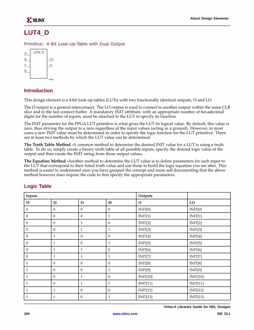
About Design Elements
LUT4_D
Primitive: 4-Bit Look-Up-Table with Dual Output
Intr oduction
This design element is a 4-bit look-up-tables (LUTs) with two functionally identical outputs, O and LO
The O output is a general interconnect. The LO output is used to connect to another output within the same CLBslice and to the fast connect buffer. A mandatory INIT attribute, with an appropriate number of hexadecimaldigits for the number of inputs, must be attached to the LUT to specify its function.
The INIT parameter for the FPGA LUT primitive is what gives the LUT its logical value. By default, this value iszero, thus driving the output to a zero regardless of the input values (acting as a ground). However, in mostcases a new INIT value must be determined in order to specify the logic function for the LUT primitive. Thereare at least two methods by which the LUT value can be determined:
The Truth Table Method -A common method to determine the desired INIT value for a LUT is using a truthtable. To do so, simply create a binary truth table of all possible inputs, specify the desired logic value of theoutput and then create the INIT string from those output values.
The Equation Method -Another method to determine the LUT value is to define parameters for each input tothe LUT that correspond to their listed truth value and use those to build the logic equation you are after. Thismethod is easier to understand once you have grasped the concept and more self-documenting that the abovemethod however does require the code to first specify the appropriate parameters.
Logic Table
Inputs Outputs
I3 I2 I1 I0 O LO
0 0 0 0 INIT[0] INIT[0]
0 0 0 1 INIT[1] INIT[1]
0 0 1 0 INIT[2] INIT[2]
0 0 1 1 INIT[3] INIT[3]
0 1 0 0 INIT[4] INIT[4]
0 1 0 1 INIT[5] INIT[5]
0 1 1 0 INIT[6] INIT[6]
0 1 1 1 INIT[7] INIT[7]
1 0 0 0 INIT[8] INIT[8]
1 0 0 1 INIT[9] INIT[9]
1 0 1 0 INIT[10] INIT[10]
1 0 1 1 INIT[11] INIT[11]
1 1 0 0 INIT[12] INIT[12]
1 1 0 1 INIT[13] INIT[13]
Vir tex-4 Libraries Guide for HDL Designs
164 www.xilinx.com ISE 10.1
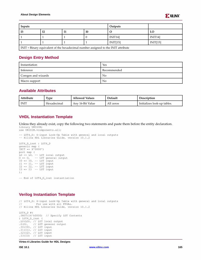
About Design Elements
Inputs Outputs
I3 I2 I1 I0 O LO
1 1 1 0 INIT14] INIT14]
1 1 1 1 INIT[15] INIT[15]
INIT = Binary equivalent of the hexadecimal number assigned to the INIT attribute
Design Entr y Method
Instantiation Yes
Inference Recommended
Coregen and wizards No
Macro support No
Availab le Attrib utes
Attribute Type Allowed Values Default Description
INIT Hexadecimal Any 16-Bit Value All zeros Initializes look-up tables.
VHDL Instantiation Template
Unless they already exist, copy the following two statements and paste them before the entity declaration.Library UNISIM;use UNISIM.vcomponents.all;
-- LUT4_D: 4-input Look-Up Table with general and local outputs-- Xilinx HDL Libraries Guide, version 10.1.2
LUT4_D_inst : LUT4_Dgeneric map (INIT => X"0000")port map (LO => LO, -- LUT local outputO => O, -- LUT general outputI0 => I0, -- LUT inputI1 => I1, -- LUT inputI2 => I2, -- LUT inputI3 => I3 -- LUT input);
-- End of LUT4_D_inst instantiation
Verilog Instantiation Template
// LUT4_D: 4-input Look-Up Table with general and local outputs// For use with all FPGAs.// Xilinx HDL Libraries Guide, version 10.1.2
LUT4_D #(.INIT(16’h0000) // Specify LUT Contents) LUT4_D_inst (.LO(LO), // LUT local output.O(O), // LUT general output.I0(I0), // LUT input.I1(I1), // LUT input.I2(I2), // LUT input.I3(I3) // LUT input
Vir tex-4 Libraries Guide for HDL Designs
ISE 10.1 www.xilinx.com 165
About Design Elements
);
// End of LUT4_D_inst instantiation
For More Information
• See the Virtex-4 User Guide.
• See the Virtex-4 Data Sheets.
Vir tex-4 Libraries Guide for HDL Designs
166 www.xilinx.com ISE 10.1
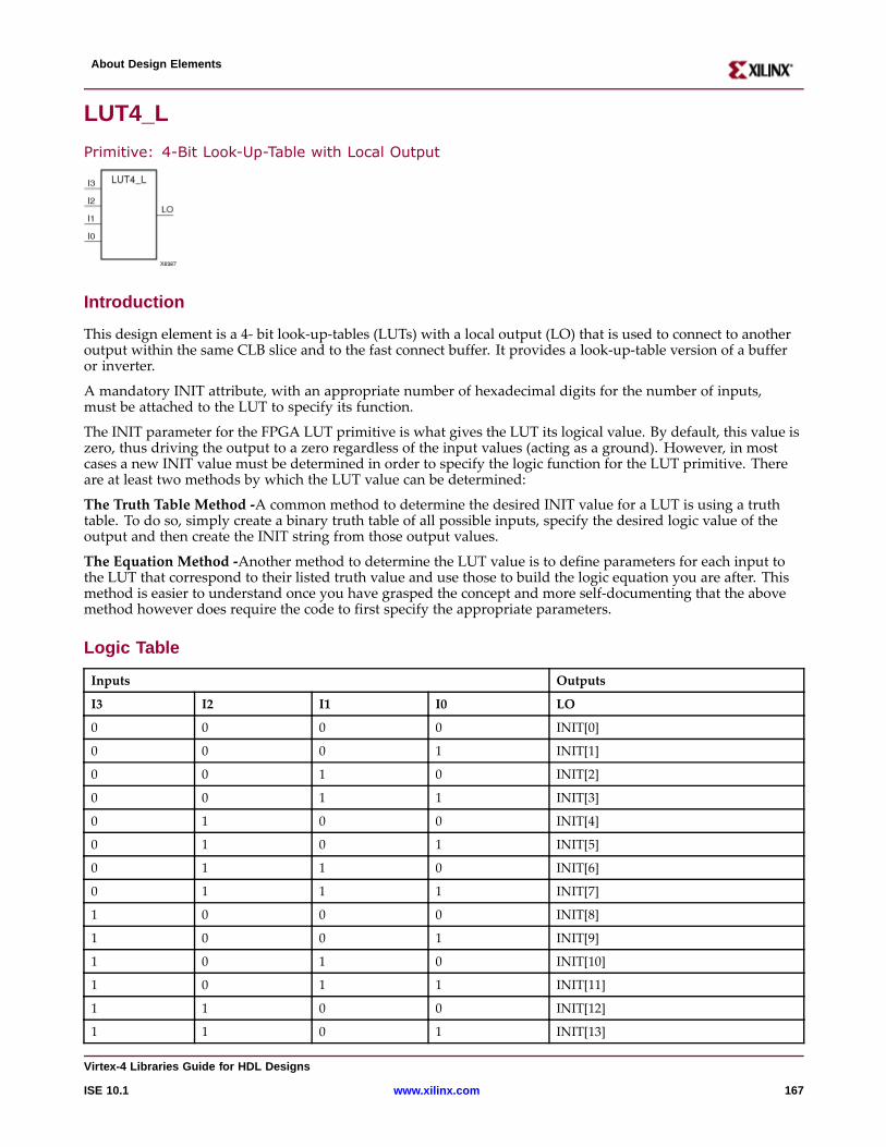
About Design Elements
LUT4_L
Primitive: 4-Bit Look-Up-Table with Local Output
Intr oduction
This design element is a 4- bit look-up-tables (LUTs) with a local output (LO) that is used to connect to anotheroutput within the same CLB slice and to the fast connect buffer. It provides a look-up-table version of a bufferor inverter.
A mandatory INIT attribute, with an appropriate number of hexadecimal digits for the number of inputs,must be attached to the LUT to specify its function.
The INIT parameter for the FPGA LUT primitive is what gives the LUT its logical value. By default, this value iszero, thus driving the output to a zero regardless of the input values (acting as a ground). However, in mostcases a new INIT value must be determined in order to specify the logic function for the LUT primitive. Thereare at least two methods by which the LUT value can be determined:
The Truth Table Method -A common method to determine the desired INIT value for a LUT is using a truthtable. To do so, simply create a binary truth table of all possible inputs, specify the desired logic value of theoutput and then create the INIT string from those output values.
The Equation Method -Another method to determine the LUT value is to define parameters for each input tothe LUT that correspond to their listed truth value and use those to build the logic equation you are after. Thismethod is easier to understand once you have grasped the concept and more self-documenting that the abovemethod however does require the code to first specify the appropriate parameters.
Logic Table
Inputs Outputs
I3 I2 I1 I0 LO
0 0 0 0 INIT[0]
0 0 0 1 INIT[1]
0 0 1 0 INIT[2]
0 0 1 1 INIT[3]
0 1 0 0 INIT[4]
0 1 0 1 INIT[5]
0 1 1 0 INIT[6]
0 1 1 1 INIT[7]
1 0 0 0 INIT[8]
1 0 0 1 INIT[9]
1 0 1 0 INIT[10]
1 0 1 1 INIT[11]
1 1 0 0 INIT[12]
1 1 0 1 INIT[13]
Vir tex-4 Libraries Guide for HDL Designs
ISE 10.1 www.xilinx.com 167
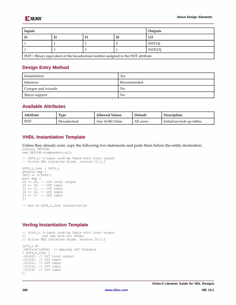
About Design Elements
Inputs Outputs
I3 I2 I1 I0 LO
1 1 1 0 INIT14]
1 1 1 1 INIT[15]
INIT = Binary equivalent of the hexadecimal number assigned to the INIT attribute
Design Entr y Method
Instantiation Yes
Inference Recommended
Coregen and wizards No
Macro support No
Availab le Attrib utes
Attribute Type Allowed Values Default Description
INIT Hexadecimal Any 16-Bit Value All zeros Initializes look-up tables.
VHDL Instantiation Template
Unless they already exist, copy the following two statements and paste them before the entity declaration.Library UNISIM;use UNISIM.vcomponents.all;
-- LUT4_L: 4-input Look-Up Table with local output-- Xilinx HDL Libraries Guide, version 10.1.2
LUT4_L_inst : LUT4_Lgeneric map (INIT => X"0000")port map (LO => LO, -- LUT local outputI0 => I0, -- LUT inputI1 => I1, -- LUT inputI2 => I2, -- LUT inputI3 => I3 -- LUT input);
-- End of LUT4_L_inst instantiation
Verilog Instantiation Template
// LUT4_L: 4-input Look-Up Table with local output// For use with all FPGAs.// Xilinx HDL Libraries Guide, version 10.1.2
LUT4_L #(.INIT(16’h0000) // Specify LUT Contents) LUT4_L_inst (.LO(LO), // LUT local output.I0(I0), // LUT input.I1(I1), // LUT input.I2(I2), // LUT input.I3(I3) // LUT input);
Vir tex-4 Libraries Guide for HDL Designs
168 www.xilinx.com ISE 10.1

About Design Elements
// End of LUT4_L_inst instantiation
For More Information
• See the Virtex-4 User Guide.
• See the Virtex-4 Data Sheets.
Vir tex-4 Libraries Guide for HDL Designs
ISE 10.1 www.xilinx.com 169
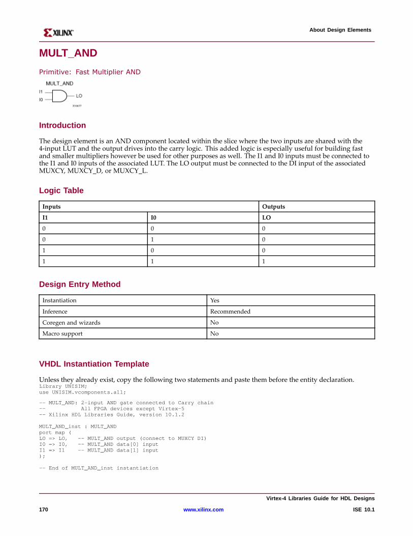
About Design Elements
MULT_AND
Primitive: Fast Multiplier AND
Intr oduction
The design element is an AND component located within the slice where the two inputs are shared with the4-input LUT and the output drives into the carry logic. This added logic is especially useful for building fastand smaller multipliers however be used for other purposes as well. The I1 and I0 inputs must be connected tothe I1 and I0 inputs of the associated LUT. The LO output must be connected to the DI input of the associatedMUXCY, MUXCY_D, or MUXCY_L.
Logic Table
Inputs Outputs
I1 I0 LO
0 0 0
0 1 0
1 0 0
1 1 1
Design Entr y Method
Instantiation Yes
Inference Recommended
Coregen and wizards No
Macro support No
VHDL Instantiation Template
Unless they already exist, copy the following two statements and paste them before the entity declaration.Library UNISIM;use UNISIM.vcomponents.all;
-- MULT_AND: 2-input AND gate connected to Carry chain-- All FPGA devices except Virtex-5-- Xilinx HDL Libraries Guide, version 10.1.2
MULT_AND_inst : MULT_ANDport map (LO => LO, -- MULT_ANDoutput (connect to MUXCYDI)I0 => I0, -- MULT_ANDdata[0] inputI1 => I1 -- MULT_ANDdata[1] input);
-- End of MULT_AND_inst instantiation
Vir tex-4 Libraries Guide for HDL Designs
170 www.xilinx.com ISE 10.1
About Design Elements
Verilog Instantiation Template
// MULT_AND: 2-input AND gate connected to Carry chain// For use with all FPGAs except Virtex-5// Xilinx HDL Libraries Guide, version 10.1.2
MULT_ANDMULT_AND_inst (.LO(LO), // MULT_ANDoutput (connect to MUXCYDI).I0(I0), // MULT_ANDdata[0] input.I1(I1) // MULT_ANDdata[1] input);
// End of MULT_AND_inst instantiation
For More Information
• See the Virtex-4 User Guide.
• See the Virtex-4 Data Sheets.
Vir tex-4 Libraries Guide for HDL Designs
ISE 10.1 www.xilinx.com 171
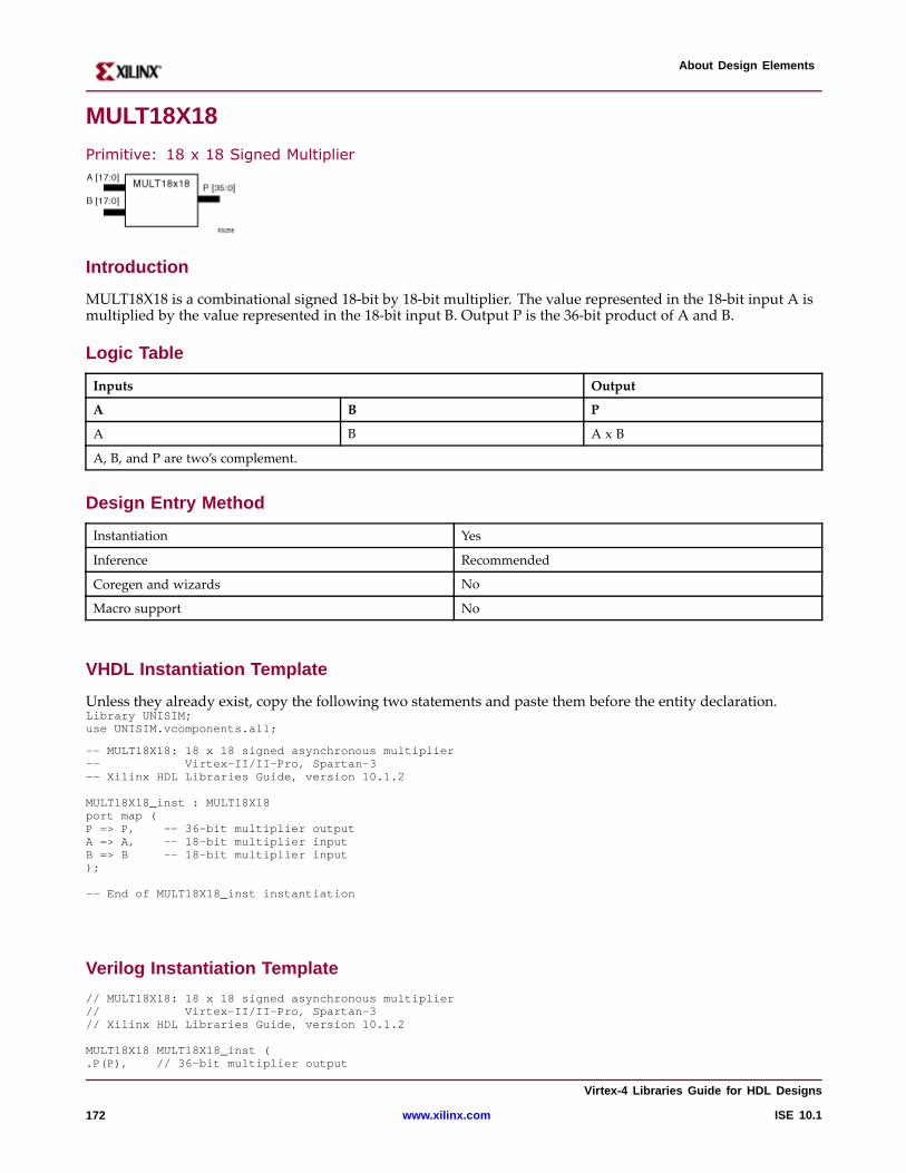
About Design Elements
MULT18X18
Primitive: 18 x 18 Signed Multiplier
Intr oduction
MULT18X18 is a combinational signed 18-bit by 18-bit multiplier. The value represented in the 18-bit input A ismultiplied by the value represented in the 18-bit input B. Output P is the 36-bit product of A and B.
Logic Table
Inputs Output
A B P
A B A x B
A, B, and P are two’s complement.
Design Entr y Method
Instantiation Yes
Inference Recommended
Coregen and wizards No
Macro support No
VHDL Instantiation Template
Unless they already exist, copy the following two statements and paste them before the entity declaration.Library UNISIM;use UNISIM.vcomponents.all;
-- MULT18X18: 18 x 18 signed asynchronous multiplier-- Virtex-II/II-Pro, Spartan-3-- Xilinx HDL Libraries Guide, version 10.1.2
MULT18X18_inst : MULT18X18port map (P => P, -- 36-bit multiplier outputA => A, -- 18-bit multiplier inputB => B -- 18-bit multiplier input);
-- End of MULT18X18_inst instantiation
Verilog Instantiation Template
// MULT18X18: 18 x 18 signed asynchronous multiplier// Virtex-II/II-Pro, Spartan-3// Xilinx HDL Libraries Guide, version 10.1.2
MULT18X18 MULT18X18_inst (.P(P), // 36-bit multiplier output
Vir tex-4 Libraries Guide for HDL Designs
172 www.xilinx.com ISE 10.1
About Design Elements
.A(A), // 18-bit multiplier input
.B(B) // 18-bit multiplier input);
// End of MULT18X18_inst instantiation
For More Information
• See the Virtex-4 User Guide.
• See the Virtex-4 Data Sheets.
Vir tex-4 Libraries Guide for HDL Designs
ISE 10.1 www.xilinx.com 173
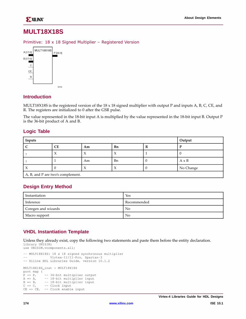
About Design Elements
MULT18X18S
Primitive: 18 x 18 Signed Multiplier – Registered Version
Intr oduction
MULT18X18S is the registered version of the 18 x 18 signed multiplier with output P and inputs A, B, C, CE, andR. The registers are initialized to 0 after the GSR pulse.
The value represented in the 18-bit input A is multiplied by the value represented in the 18-bit input B. Output Pis the 36-bit product of A and B.
Logic Table
Inputs Output
C CE Am Bn R P
↑ X X X 1 0
↑ 1 Am Bn 0 A x B
X 0 X X 0 No Change
A, B, and P are two’s complement.
Design Entr y Method
Instantiation Yes
Inference Recommended
Coregen and wizards No
Macro support No
VHDL Instantiation Template
Unless they already exist, copy the following two statements and paste them before the entity declaration.Library UNISIM;use UNISIM.vcomponents.all;
-- MULT18X18S: 18 x 18 signed synchronous multiplier-- Virtex-II/II-Pro, Spartan-3-- Xilinx HDL Libraries Guide, version 10.1.2
MULT18X18S_inst : MULT18X18Sport map (P => P, -- 36-bit multiplier outputA => A, -- 18-bit multiplier inputB => B, -- 18-bit multiplier inputC => C, -- Clock inputCE => CE, -- Clock enable input
Vir tex-4 Libraries Guide for HDL Designs
174 www.xilinx.com ISE 10.1
About Design Elements
R => R -- Synchronous reset input);
-- End of MULT18X18S_inst instantiation
Verilog Instantiation Template
// MULT18X18S: 18 x 18 signed synchronous multiplier// Virtex-II/II-Pro, Spartan-3// Xilinx HDL Libraries Guide, version 10.1.2
MULT18X18S MULT18X18S_inst (.P(P), // 36-bit multiplier output.A(A), // 18-bit multiplier input.B(B), // 18-bit multiplier input.C(C), // Clock input.CE(CE), // Clock enable input.R(R) // Synchronous reset input);
// End of MULT18X18S_inst instantiation
For More Information
• See the Virtex-4 User Guide.
• See the Virtex-4 Data Sheets.
Vir tex-4 Libraries Guide for HDL Designs
ISE 10.1 www.xilinx.com 175
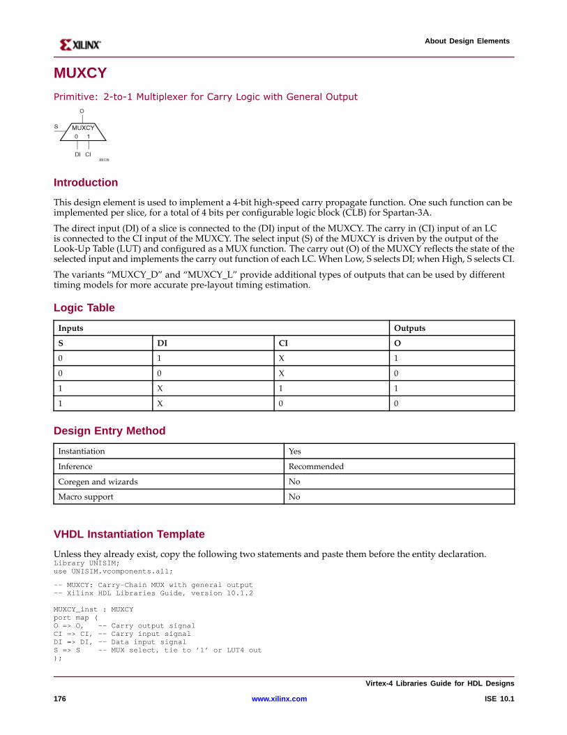
About Design Elements
MUXCY
Primitive: 2-to-1 Multiplexer for Carry Logic with General Output
Intr oduction
This design element is used to implement a 4-bit high-speed carry propagate function. One such function can beimplemented per slice, for a total of 4 bits per configurable logic block (CLB) for Spartan-3A.
The direct input (DI) of a slice is connected to the (DI) input of the MUXCY. The carry in (CI) input of an LCis connected to the CI input of the MUXCY. The select input (S) of the MUXCY is driven by the output of theLook-Up Table (LUT) and configured as a MUX function. The carry out (O) of the MUXCY reflects the state of theselected input and implements the carry out function of each LC. When Low, S selects DI; when High, S selects CI.
The variants “MUXCY_D” and “MUXCY_L” provide additional types of outputs that can be used by differenttiming models for more accurate pre-layout timing estimation.
Logic Table
Inputs Outputs
S DI CI O
0 1 X 1
0 0 X 0
1 X 1 1
1 X 0 0
Design Entr y Method
Instantiation Yes
Inference Recommended
Coregen and wizards No
Macro support No
VHDL Instantiation Template
Unless they already exist, copy the following two statements and paste them before the entity declaration.Library UNISIM;use UNISIM.vcomponents.all;
-- MUXCY: Carry-Chain MUXwith general output-- Xilinx HDL Libraries Guide, version 10.1.2
MUXCY_inst : MUXCYport map (O => O, -- Carry output signalCI => CI, -- Carry input signalDI => DI, -- Data input signalS => S -- MUX select, tie to ’1’ or LUT4 out);
Vir tex-4 Libraries Guide for HDL Designs
176 www.xilinx.com ISE 10.1
About Design Elements
-- End of MUXCY_inst instantiation
Verilog Instantiation Template
// MUXCY: Carry-Chain MUXwith general output// For use with All FPGAs// Xilinx HDL Libraries Guide, version 10.1.2
MUXCYMUXCY_inst (.O(O), // Carry output signal.CI(CI), // Carry input signal.DI(DI), // Data input signal.S(S) // MUX select, tie to ’1’ or LUT4 out);
// End of MUXCY_inst instantiation
For More Information
• See the Virtex-4 User Guide.
• See the Virtex-4 Data Sheets.
Vir tex-4 Libraries Guide for HDL Designs
ISE 10.1 www.xilinx.com 177
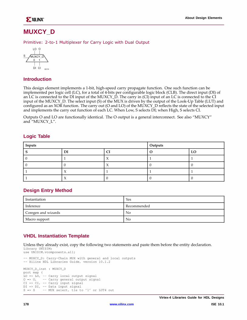
About Design Elements
MUXCY_D
Primitive: 2-to-1 Multiplexer for Carry Logic with Dual Output
Intr oduction
This design element implements a 1-bit, high-speed carry propagate function. One such function can beimplemented per logic cell (LC), for a total of 4-bits per configurable logic block (CLB). The direct input (DI) ofan LC is connected to the DI input of the MUXCY_D. The carry in (CI) input of an LC is connected to the CIinput of the MUXCY_D. The select input (S) of the MUX is driven by the output of the Look-Up Table (LUT) andconfigured as an XOR function. The carry out (O and LO) of the MUXCY_D reflects the state of the selected inputand implements the carry out function of each LC. When Low, S selects DI; when High, S selects CI.
Outputs O and LO are functionally identical. The O output is a general interconnect. See also “MUXCY”and “MUXCY_L”.
Logic Table
Inputs Outputs
S DI CI O LO
0 1 X 1 1
0 0 X 0 0
1 X 1 1 1
1 X 0 0 0
Design Entr y Method
Instantiation Yes
Inference Recommended
Coregen and wizards No
Macro support No
VHDL Instantiation Template
Unless they already exist, copy the following two statements and paste them before the entity declaration.Library UNISIM;use UNISIM.vcomponents.all;
-- MUXCY_D: Carry-Chain MUXwith general and local outputs-- Xilinx HDL Libraries Guide, version 10.1.2
MUXCY_D_inst : MUXCY_Dport map (LO => LO, -- Carry local output signalO => O, -- Carry general output signalCI => CI, -- Carry input signalDI => DI, -- Data input signalS => S -- MUX select, tie to ’1’ or LUT4 out
Vir tex-4 Libraries Guide for HDL Designs
178 www.xilinx.com ISE 10.1
About Design Elements
);
-- End of MUXCY_D_inst instantiation
Verilog Instantiation Template
// MUXCY_D: Carry-Chain MUXwith general and local outputs// For use with All FPGAs// Xilinx HDL Libraries Guide, version 10.1.2
MUXCY_DMUXCY_D_inst (.LO(LO), // Carry local output signal.O(O), // Carry general output signal.CI(CI), // Carry input signal.DI(DI), // Data input signal.S(S) // MUX select, tie to ’1’ or LUT4 out);
// End of MUXCY_D_inst instantiation
For More Information
• See the Virtex-4 User Guide.
• See the Virtex-4 Data Sheets.
Vir tex-4 Libraries Guide for HDL Designs
ISE 10.1 www.xilinx.com 179
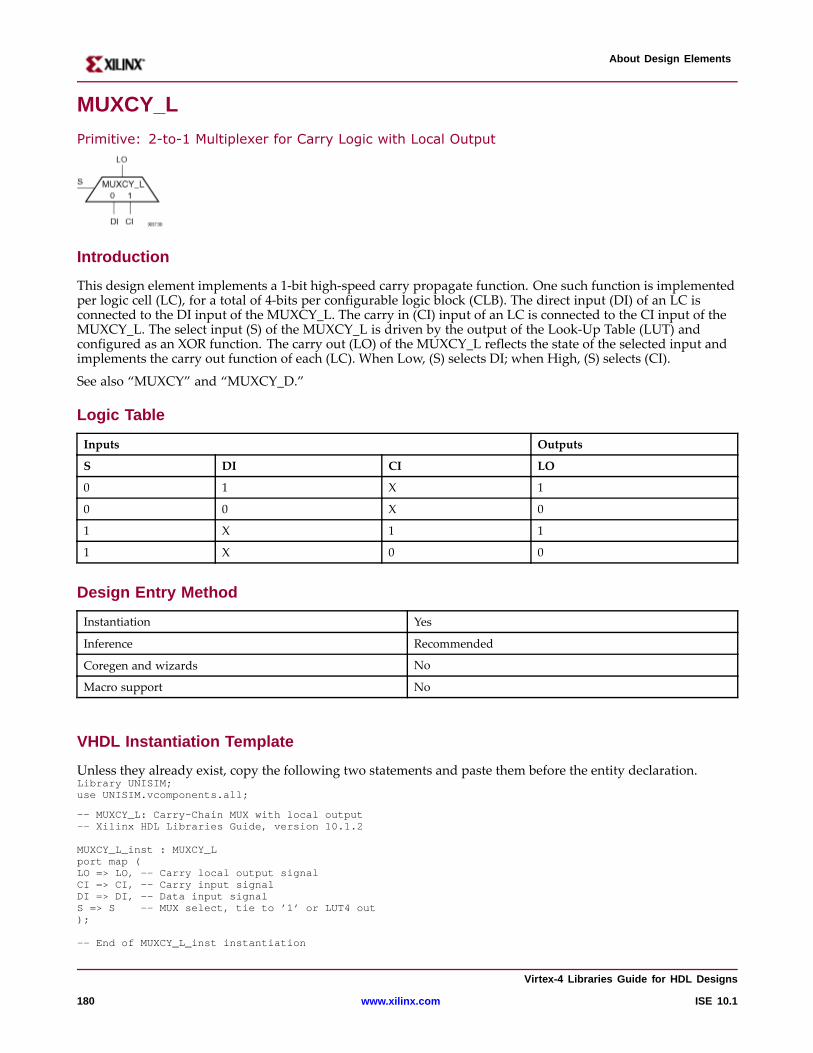
About Design Elements
MUXCY_L
Primitive: 2-to-1 Multiplexer for Carry Logic with Local Output
Intr oduction
This design element implements a 1-bit high-speed carry propagate function. One such function is implementedper logic cell (LC), for a total of 4-bits per configurable logic block (CLB). The direct input (DI) of an LC isconnected to the DI input of the MUXCY_L. The carry in (CI) input of an LC is connected to the CI input of theMUXCY_L. The select input (S) of the MUXCY_L is driven by the output of the Look-Up Table (LUT) andconfigured as an XOR function. The carry out (LO) of the MUXCY_L reflects the state of the selected input andimplements the carry out function of each (LC). When Low, (S) selects DI; when High, (S) selects (CI).
See also “MUXCY” and “MUXCY_D.”
Logic Table
Inputs Outputs
S DI CI LO
0 1 X 1
0 0 X 0
1 X 1 1
1 X 0 0
Design Entr y Method
Instantiation Yes
Inference Recommended
Coregen and wizards No
Macro support No
VHDL Instantiation Template
Unless they already exist, copy the following two statements and paste them before the entity declaration.Library UNISIM;use UNISIM.vcomponents.all;
-- MUXCY_L: Carry-Chain MUXwith local output-- Xilinx HDL Libraries Guide, version 10.1.2
MUXCY_L_inst : MUXCY_Lport map (LO => LO, -- Carry local output signalCI => CI, -- Carry input signalDI => DI, -- Data input signalS => S -- MUX select, tie to ’1’ or LUT4 out);
-- End of MUXCY_L_inst instantiation
Vir tex-4 Libraries Guide for HDL Designs
180 www.xilinx.com ISE 10.1

About Design Elements
Verilog Instantiation Template
// MUXCY_L: Carry-Chain MUXwith local output// For use with All FPGAs// Xilinx HDL Libraries Guide, version 10.1.2
MUXCY_LMUXCY_L_inst (.LO(LO), // Carry local output signal.CI(CI), // Carry input signal.DI(DI), // Data input signal.S(S) // MUX select, tie to ’1’ or LUT4 out);
// End of MUXCY_L_inst instantiation
For More Information
• See the Virtex-4 User Guide.
• See the Virtex-4 Data Sheets.
Vir tex-4 Libraries Guide for HDL Designs
ISE 10.1 www.xilinx.com 181
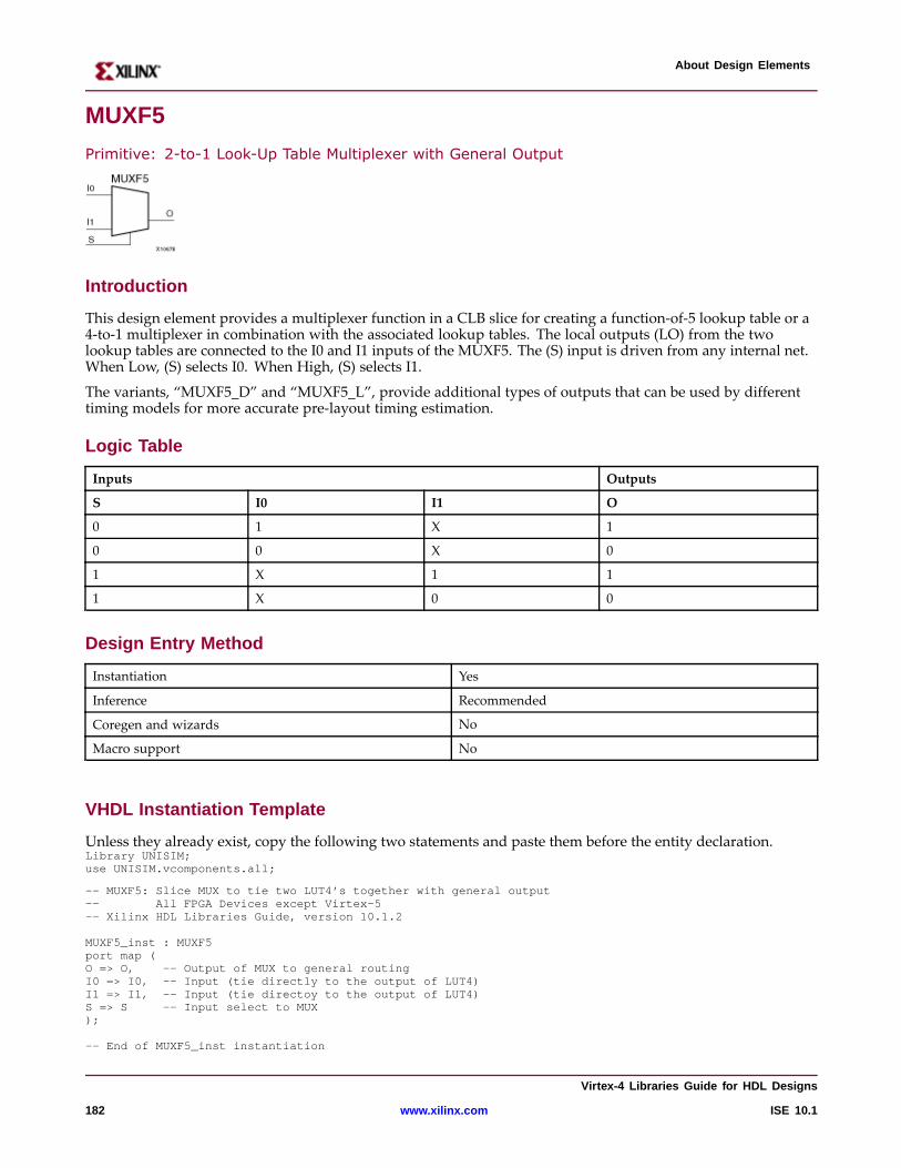
About Design Elements
MUXF5
Primitive: 2-to-1 Look-Up Table Multiplexer with General Output
Intr oduction
This design element provides a multiplexer function in a CLB slice for creating a function-of-5 lookup table or a4-to-1 multiplexer in combination with the associated lookup tables. The local outputs (LO) from the twolookup tables are connected to the I0 and I1 inputs of the MUXF5. The (S) input is driven from any internal net.When Low, (S) selects I0. When High, (S) selects I1.
The variants, “MUXF5_D” and “MUXF5_L”, provide additional types of outputs that can be used by differenttiming models for more accurate pre-layout timing estimation.
Logic Table
Inputs Outputs
S I0 I1 O
0 1 X 1
0 0 X 0
1 X 1 1
1 X 0 0
Design Entr y Method
Instantiation Yes
Inference Recommended
Coregen and wizards No
Macro support No
VHDL Instantiation Template
Unless they already exist, copy the following two statements and paste them before the entity declaration.Library UNISIM;use UNISIM.vcomponents.all;
-- MUXF5: Slice MUX to tie two LUT4’s together with general output-- All FPGA Devices except Virtex-5-- Xilinx HDL Libraries Guide, version 10.1.2
MUXF5_inst : MUXF5port map (O => O, -- Output of MUX to general routingI0 => I0, -- Input (tie directly to the output of LUT4)I1 => I1, -- Input (tie directoy to the output of LUT4)S => S -- Input select to MUX);
-- End of MUXF5_inst instantiation
Vir tex-4 Libraries Guide for HDL Designs
182 www.xilinx.com ISE 10.1

About Design Elements
Verilog Instantiation Template
// MUXF5: Slice MUX to tie two LUT4’s together with general output// For use with All FPGAs except Virtex-5// Xilinx HDL Libraries Guide, version 10.1.2
MUXF5MUXF5_inst (.O(O), // Output of MUX to general routing.I0(I0), // Input (tie directly to the output of LUT4).I1(I1), // Input (tie directoy to the output of LUT4).S(S) // Input select to MUX);
// End of MUXF5_inst instantiation
For More Information
• See the Virtex-4 User Guide.
• See the Virtex-4 Data Sheets.
Vir tex-4 Libraries Guide for HDL Designs
ISE 10.1 www.xilinx.com 183
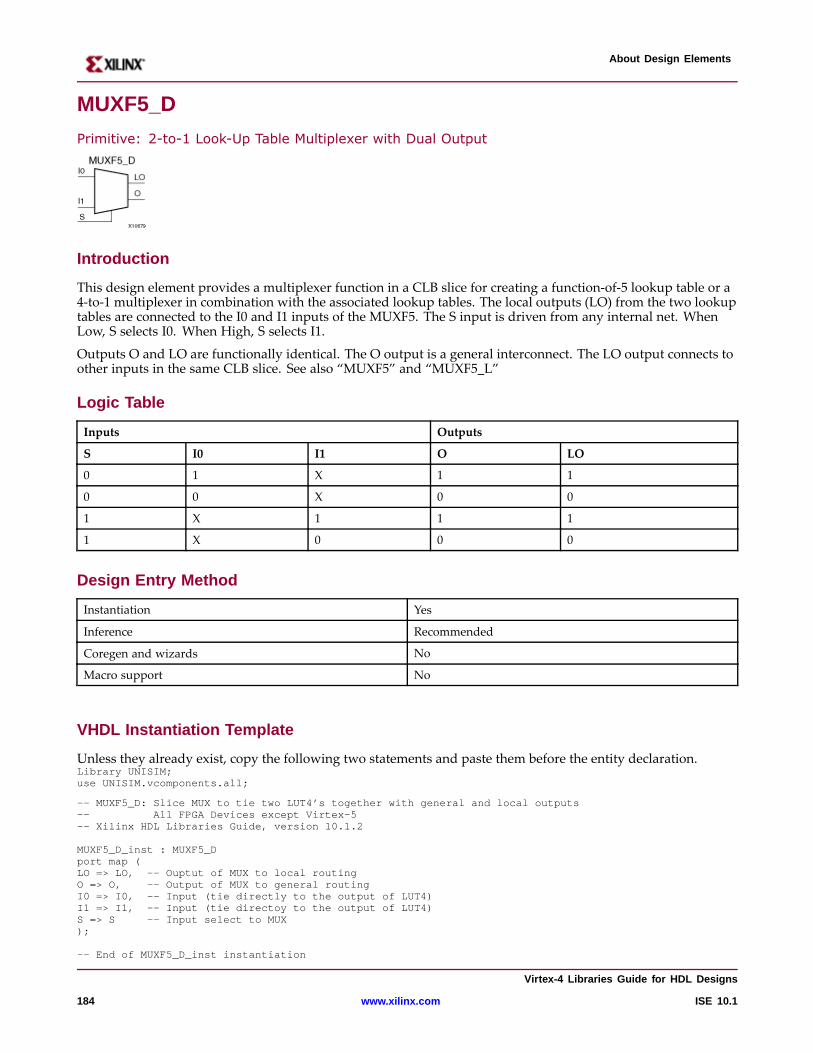
About Design Elements
MUXF5_D
Primitive: 2-to-1 Look-Up Table Multiplexer with Dual Output
Intr oduction
This design element provides a multiplexer function in a CLB slice for creating a function-of-5 lookup table or a4-to-1 multiplexer in combination with the associated lookup tables. The local outputs (LO) from the two lookuptables are connected to the I0 and I1 inputs of the MUXF5. The S input is driven from any internal net. WhenLow, S selects I0. When High, S selects I1.
Outputs O and LO are functionally identical. The O output is a general interconnect. The LO output connects toother inputs in the same CLB slice. See also “MUXF5” and “MUXF5_L”
Logic Table
Inputs Outputs
S I0 I1 O LO
0 1 X 1 1
0 0 X 0 0
1 X 1 1 1
1 X 0 0 0
Design Entr y Method
Instantiation Yes
Inference Recommended
Coregen and wizards No
Macro support No
VHDL Instantiation Template
Unless they already exist, copy the following two statements and paste them before the entity declaration.Library UNISIM;use UNISIM.vcomponents.all;
-- MUXF5_D: Slice MUX to tie two LUT4’s together with general and local outputs-- All FPGA Devices except Virtex-5-- Xilinx HDL Libraries Guide, version 10.1.2
MUXF5_D_inst : MUXF5_Dport map (LO => LO, -- Ouptut of MUX to local routingO => O, -- Output of MUX to general routingI0 => I0, -- Input (tie directly to the output of LUT4)I1 => I1, -- Input (tie directoy to the output of LUT4)S => S -- Input select to MUX);
-- End of MUXF5_D_inst instantiation
Vir tex-4 Libraries Guide for HDL Designs
184 www.xilinx.com ISE 10.1
About Design Elements
Verilog Instantiation Template
// MUXF5_D: Slice MUX to tie two LUT4’s together with general and local outputs// For use with All FPGAs except Virtex-5// Xilinx HDL Libraries Guide, version 10.1.2
MUXF5_DMUXF5_D_inst (.LO(LO), // Ouptut of MUX to local routing.O(O), // Output of MUX to general routing.I0(I0), // Input (tie directly to the output of LUT4).I1(I1), // Input (tie directoy to the output of LUT4).S(S) // Input select to MUX);
// End of MUXF5_D_inst instantiation
For More Information
• See the Virtex-4 User Guide.
• See the Virtex-4 Data Sheets.
Vir tex-4 Libraries Guide for HDL Designs
ISE 10.1 www.xilinx.com 185
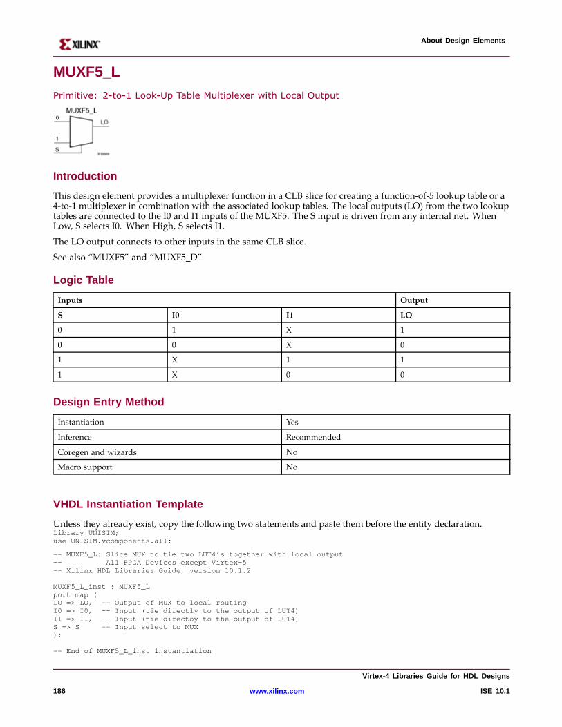
About Design Elements
MUXF5_L
Primitive: 2-to-1 Look-Up Table Multiplexer with Local Output
Intr oduction
This design element provides a multiplexer function in a CLB slice for creating a function-of-5 lookup table or a4-to-1 multiplexer in combination with the associated lookup tables. The local outputs (LO) from the two lookuptables are connected to the I0 and I1 inputs of the MUXF5. The S input is driven from any internal net. WhenLow, S selects I0. When High, S selects I1.
The LO output connects to other inputs in the same CLB slice.
See also “MUXF5” and “MUXF5_D”
Logic Table
Inputs Output
S I0 I1 LO
0 1 X 1
0 0 X 0
1 X 1 1
1 X 0 0
Design Entr y Method
Instantiation Yes
Inference Recommended
Coregen and wizards No
Macro support No
VHDL Instantiation Template
Unless they already exist, copy the following two statements and paste them before the entity declaration.Library UNISIM;use UNISIM.vcomponents.all;
-- MUXF5_L: Slice MUX to tie two LUT4’s together with local output-- All FPGA Devices except Virtex-5-- Xilinx HDL Libraries Guide, version 10.1.2
MUXF5_L_inst : MUXF5_Lport map (LO => LO, -- Output of MUX to local routingI0 => I0, -- Input (tie directly to the output of LUT4)I1 => I1, -- Input (tie directoy to the output of LUT4)S => S -- Input select to MUX);
-- End of MUXF5_L_inst instantiation
Vir tex-4 Libraries Guide for HDL Designs
186 www.xilinx.com ISE 10.1
About Design Elements
Verilog Instantiation Template
// MUXF5_L: Slice MUX to tie two LUT4’s together with local output// For use with All FPGAs except Virtex-5// Xilinx HDL Libraries Guide, version 10.1.2
MUXF5_L MUXF5_L_inst (.LO(LO), // Output of MUX to local routing.I0(I0), // Input (tie directly to the output of LUT4).I1(I1), // Input (tie directoy to the output of LUT4).S(S) // Input select to MUX);
// End of MUXF5_L_inst instantiation
For More Information
• See the Virtex-4 User Guide.
• See the Virtex-4 Data Sheets.
Vir tex-4 Libraries Guide for HDL Designs
ISE 10.1 www.xilinx.com 187
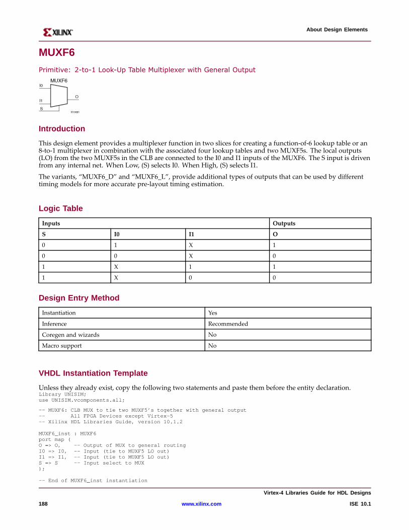
About Design Elements
MUXF6
Primitive: 2-to-1 Look-Up Table Multiplexer with General Output
Intr oduction
This design element provides a multiplexer function in two slices for creating a function-of-6 lookup table or an8-to-1 multiplexer in combination with the associated four lookup tables and two MUXF5s. The local outputs(LO) from the two MUXF5s in the CLB are connected to the I0 and I1 inputs of the MUXF6. The S input is drivenfrom any internal net. When Low, (S) selects I0. When High, (S) selects I1.
The variants, “MUXF6_D” and “MUXF6_L”, provide additional types of outputs that can be used by differenttiming models for more accurate pre-layout timing estimation.
Logic Table
Inputs Outputs
S I0 I1 O
0 1 X 1
0 0 X 0
1 X 1 1
1 X 0 0
Design Entr y Method
Instantiation Yes
Inference Recommended
Coregen and wizards No
Macro support No
VHDL Instantiation Template
Unless they already exist, copy the following two statements and paste them before the entity declaration.Library UNISIM;use UNISIM.vcomponents.all;
-- MUXF6: CLB MUX to tie two MUXF5’s together with general output-- All FPGA Devices except Virtex-5-- Xilinx HDL Libraries Guide, version 10.1.2
MUXF6_inst : MUXF6port map (O => O, -- Output of MUX to general routingI0 => I0, -- Input (tie to MUXF5 LO out)I1 => I1, -- Input (tie to MUXF5 LO out)S => S -- Input select to MUX);
-- End of MUXF6_inst instantiation
Vir tex-4 Libraries Guide for HDL Designs
188 www.xilinx.com ISE 10.1
About Design Elements
Verilog Instantiation Template
// MUXF6: CLB MUX to tie two MUXF5’s together with general output// For use with All FPGAs except Virtex-5// Xilinx HDL Libraries Guide, version 10.1.2
MUXF6MUXF6_inst (.O(O), // Output of MUX to general routing.I0(I0), // Input (tie to MUXF5 LO out).I1(I1), // Input (tie to MUXF5 LO out).S(S) // Input select to MUX);
// End of MUXF6_inst instantiation
For More Information
• See the Virtex-4 User Guide.
• See the Virtex-4 Data Sheets.
Vir tex-4 Libraries Guide for HDL Designs
ISE 10.1 www.xilinx.com 189
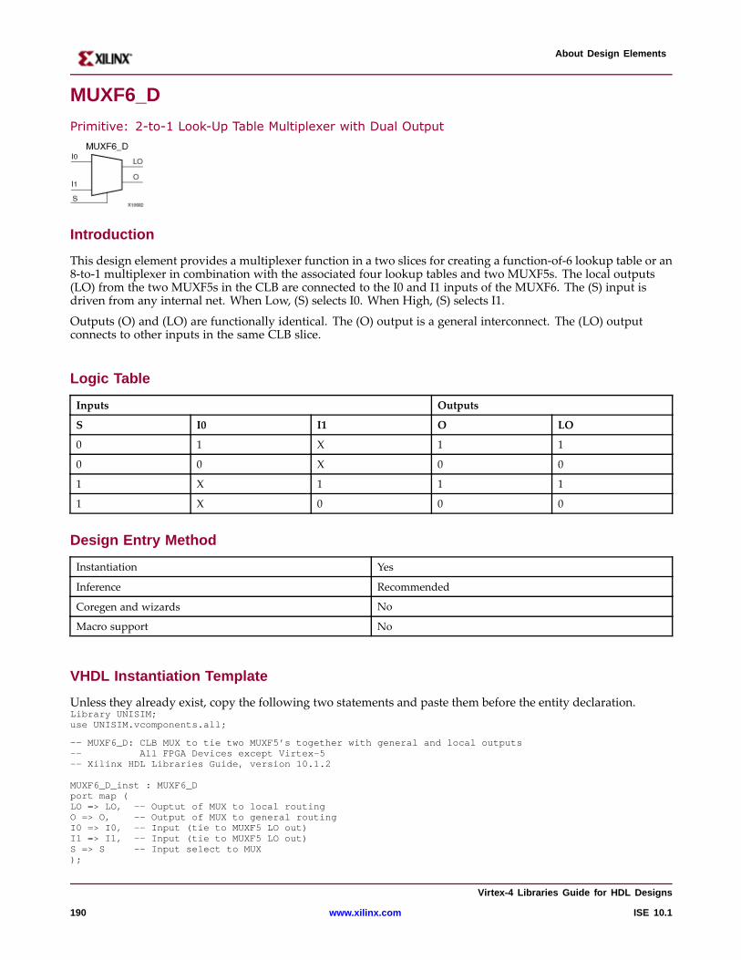
About Design Elements
MUXF6_D
Primitive: 2-to-1 Look-Up Table Multiplexer with Dual Output
Intr oduction
This design element provides a multiplexer function in a two slices for creating a function-of-6 lookup table or an8-to-1 multiplexer in combination with the associated four lookup tables and two MUXF5s. The local outputs(LO) from the two MUXF5s in the CLB are connected to the I0 and I1 inputs of the MUXF6. The (S) input isdriven from any internal net. When Low, (S) selects I0. When High, (S) selects I1.
Outputs (O) and (LO) are functionally identical. The (O) output is a general interconnect. The (LO) outputconnects to other inputs in the same CLB slice.
Logic Table
Inputs Outputs
S I0 I1 O LO
0 1 X 1 1
0 0 X 0 0
1 X 1 1 1
1 X 0 0 0
Design Entr y Method
Instantiation Yes
Inference Recommended
Coregen and wizards No
Macro support No
VHDL Instantiation Template
Unless they already exist, copy the following two statements and paste them before the entity declaration.Library UNISIM;use UNISIM.vcomponents.all;
-- MUXF6_D: CLB MUX to tie two MUXF5’s together with general and local outputs-- All FPGA Devices except Virtex-5-- Xilinx HDL Libraries Guide, version 10.1.2
MUXF6_D_inst : MUXF6_Dport map (LO => LO, -- Ouptut of MUX to local routingO => O, -- Output of MUX to general routingI0 => I0, -- Input (tie to MUXF5 LO out)I1 => I1, -- Input (tie to MUXF5 LO out)S => S -- Input select to MUX);
Vir tex-4 Libraries Guide for HDL Designs
190 www.xilinx.com ISE 10.1
About Design Elements
-- End of MUXF6_D_inst instantiation
Verilog Instantiation Template
// MUXF6_D: CLB MUX to tie two MUXF5’s together with general and local outputs// For use with All FPGAs except Virtex-5// Xilinx HDL Libraries Guide, version 10.1.2
MUXF6_DMUXF6_D_inst (.LO(LO), // Ouptut of MUX to local routing.O(O), // Output of MUX to general routing.I0(I0), // Input (tie to MUXF5 LO out).I1(I1), // Input (tie to MUXF5 LO out).S(S) // Input select to MUX);
// End of MUXF6_D_inst instantiation
For More Information
• See the Virtex-4 User Guide.
• See the Virtex-4 Data Sheets.
Vir tex-4 Libraries Guide for HDL Designs
ISE 10.1 www.xilinx.com 191
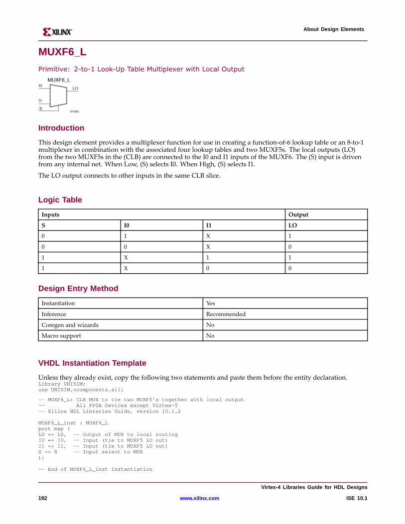
About Design Elements
MUXF6_L
Primitive: 2-to-1 Look-Up Table Multiplexer with Local Output
Intr oduction
This design element provides a multiplexer function for use in creating a function-of-6 lookup table or an 8-to-1multiplexer in combination with the associated four lookup tables and two MUXF5s. The local outputs (LO)from the two MUXF5s in the (CLB) are connected to the I0 and I1 inputs of the MUXF6. The (S) input is drivenfrom any internal net. When Low, (S) selects I0. When High, (S) selects I1.
The LO output connects to other inputs in the same CLB slice.
Logic Table
Inputs Output
S I0 I1 LO
0 1 X 1
0 0 X 0
1 X 1 1
1 X 0 0
Design Entr y Method
Instantiation Yes
Inference Recommended
Coregen and wizards No
Macro support No
VHDL Instantiation Template
Unless they already exist, copy the following two statements and paste them before the entity declaration.Library UNISIM;use UNISIM.vcomponents.all;
-- MUXF6_L: CLB MUX to tie two MUXF5’s together with local output-- All FPGA Devices except Virtex-5-- Xilinx HDL Libraries Guide, version 10.1.2
MUXF6_L_inst : MUXF6_Lport map (LO => LO, -- Output of MUX to local routingI0 => I0, -- Input (tie to MUXF5 LO out)I1 => I1, -- Input (tie to MUXF5 LO out)S => S -- Input select to MUX);
-- End of MUXF6_L_inst instantiation
Vir tex-4 Libraries Guide for HDL Designs
192 www.xilinx.com ISE 10.1
About Design Elements
Verilog Instantiation Template
// MUXF6_L: CLB MUX to tie two MUXF5’s together with local output// For use with All FPGAs except Virtex-5// Xilinx HDL Libraries Guide, version 10.1.2
MUXF6_L MUXF6_L_inst (.LO(LO), // Output of MUX to local routing.I0(I0), // Input (tie to MUXF5 LO out).I1(I1), // Input (tie to MUXF5 LO out).S(S) // Input select to MUX);
// End of MUXF6_L_inst instantiation
For More Information
• See the Virtex-4 User Guide.
• See the Virtex-4 Data Sheets.
Vir tex-4 Libraries Guide for HDL Designs
ISE 10.1 www.xilinx.com 193
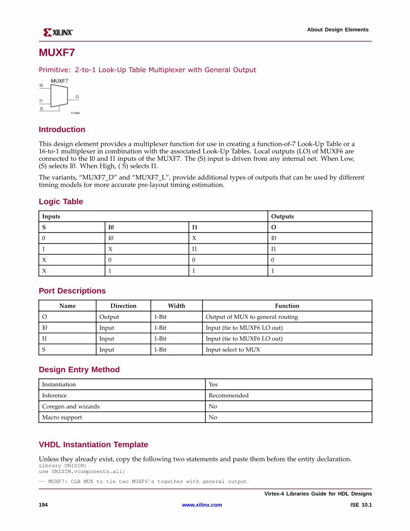
About Design Elements
MUXF7
Primitive: 2-to-1 Look-Up Table Multiplexer with General Output
Intr oduction
This design element provides a multiplexer function for use in creating a function-of-7 Look-Up Table or a16-to-1 multiplexer in combination with the associated Look-Up Tables. Local outputs (LO) of MUXF6 areconnected to the I0 and I1 inputs of the MUXF7. The (S) input is driven from any internal net. When Low,(S) selects I0. When High, ( S) selects I1.
The variants, “MUXF7_D” and “MUXF7_L”, provide additional types of outputs that can be used by differenttiming models for more accurate pre-layout timing estimation.
Logic Table
Inputs Outputs
S I0 I1 O
0 I0 X I0
1 X I1 I1
X 0 0 0
X 1 1 1
Por t Descriptions
Name Direction Width Function
O Output 1-Bit Output of MUX to general routing
I0 Input 1-Bit Input (tie to MUXF6 LO out)
I1 Input 1-Bit Input (tie to MUXF6 LO out)
S Input 1-Bit Input select to MUX
Design Entr y Method
Instantiation Yes
Inference Recommended
Coregen and wizards No
Macro support No
VHDL Instantiation Template
Unless they already exist, copy the following two statements and paste them before the entity declaration.Library UNISIM;use UNISIM.vcomponents.all;
-- MUXF7: CLB MUX to tie two MUXF6’s together with general output
Vir tex-4 Libraries Guide for HDL Designs
194 www.xilinx.com ISE 10.1

About Design Elements
-- Virtex-II/II-Pro/4/5 and Spartan-3/3E/3A-- Xilinx HDL Libraries Guide, version 10.1.2
MUXF7_inst : MUXF7port map (O => O, -- Output of MUX to general routingI0 => I0, -- Input (tie to MUXF6 LO out)I1 => I1, -- Input (tie to MUXF6 LO out)S => S -- Input select to MUX);
-- End of MUXF7_inst instantiation
Verilog Instantiation Template
// MUXF7: CLB MUX to tie two LUT6’s or MUXF6’s together with general output// For use with Virtex-II/II-Pro/4/5 and Spartan-3/3E/3A// Xilinx HDL Libraries Guide, version 10.1.2
MUXF7MUXF7_inst (.O(O), // Output of MUX to general routing.I0(I0), // Input (tie to MUXF6 LO out).I1(I1), // Input (tie to MUXF6 LO out).S(S) // Input select to MUX);
// End of MUXF7_inst instantiation
For More Information
• See the Virtex-4 User Guide.
• See the Virtex-4 Data Sheets.
Vir tex-4 Libraries Guide for HDL Designs
ISE 10.1 www.xilinx.com 195
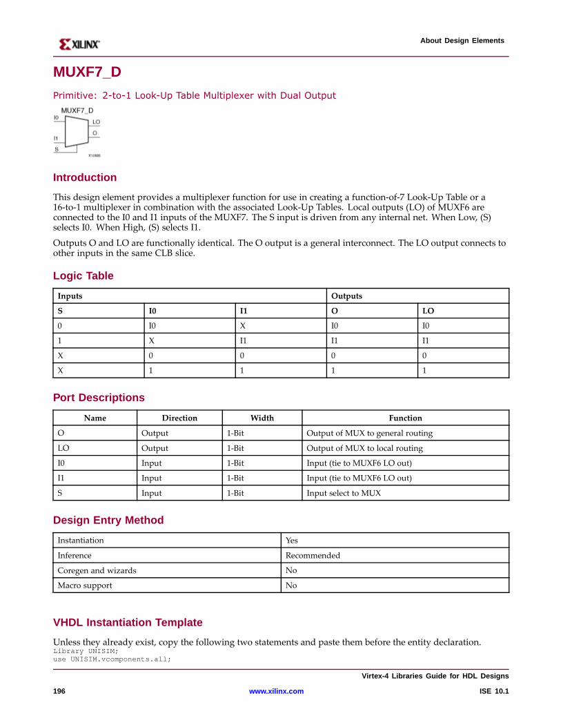
About Design Elements
MUXF7_D
Primitive: 2-to-1 Look-Up Table Multiplexer with Dual Output
Intr oduction
This design element provides a multiplexer function for use in creating a function-of-7 Look-Up Table or a16-to-1 multiplexer in combination with the associated Look-Up Tables. Local outputs (LO) of MUXF6 areconnected to the I0 and I1 inputs of the MUXF7. The S input is driven from any internal net. When Low, (S)selects I0. When High, (S) selects I1.
Outputs O and LO are functionally identical. The O output is a general interconnect. The LO output connects toother inputs in the same CLB slice.
Logic Table
Inputs Outputs
S I0 I1 O LO
0 I0 X I0 I0
1 X I1 I1 I1
X 0 0 0 0
X 1 1 1 1
Por t Descriptions
Name Direction Width Function
O Output 1-Bit Output of MUX to general routing
LO Output 1-Bit Output of MUX to local routing
I0 Input 1-Bit Input (tie to MUXF6 LO out)
I1 Input 1-Bit Input (tie to MUXF6 LO out)
S Input 1-Bit Input select to MUX
Design Entr y Method
Instantiation Yes
Inference Recommended
Coregen and wizards No
Macro support No
VHDL Instantiation Template
Unless they already exist, copy the following two statements and paste them before the entity declaration.Library UNISIM;use UNISIM.vcomponents.all;
Vir tex-4 Libraries Guide for HDL Designs
196 www.xilinx.com ISE 10.1
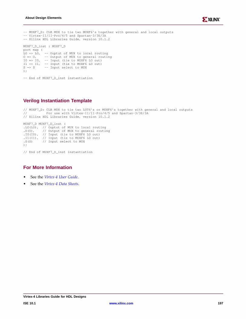
About Design Elements
-- MUXF7_D: CLB MUX to tie two MUXF6’s together with general and local outputs-- Virtex-II/II-Pro/4/5 and Spartan-3/3E/3A-- Xilinx HDL Libraries Guide, version 10.1.2
MUXF7_D_inst : MUXF7_Dport map (LO => LO, -- Ouptut of MUX to local routingO => O, -- Output of MUX to general routingI0 => I0, -- Input (tie to MUXF6 LO out)I1 => I1, -- Input (tie to MUXF6 LO out)S => S -- Input select to MUX);
-- End of MUXF7_D_inst instantiation
Verilog Instantiation Template
// MUXF7_D: CLB MUX to tie two LUT6’s or MUXF6’s together with general and local outputs// For use with Virtex-II/II-Pro/4/5 and Spartan-3/3E/3A// Xilinx HDL Libraries Guide, version 10.1.2
MUXF7_DMUXF7_D_inst (.LO(LO), // Ouptut of MUX to local routing.O(O), // Output of MUX to general routing.I0(I0), // Input (tie to MUXF6 LO out).I1(I1), // Input (tie to MUXF6 LO out).S(S) // Input select to MUX);
// End of MUXF7_D_inst instantiation
For More Information
• See the Virtex-4 User Guide.
• See the Virtex-4 Data Sheets.
Vir tex-4 Libraries Guide for HDL Designs
ISE 10.1 www.xilinx.com 197
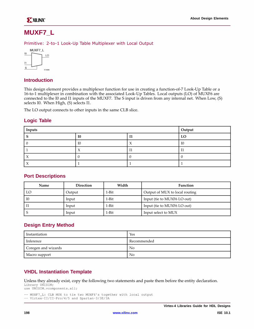
About Design Elements
MUXF7_L
Primitive: 2-to-1 Look-Up Table Multiplexer with Local Output
Intr oduction
This design element provides a multiplexer function for use in creating a function-of-7 Look-Up Table or a16-to-1 multiplexer in combination with the associated Look-Up Tables. Local outputs (LO) of MUXF6 areconnected to the I0 and I1 inputs of the MUXF7. The S input is driven from any internal net. When Low, (S)selects I0. When High, (S) selects I1.
The LO output connects to other inputs in the same CLB slice.
Logic Table
Inputs Output
S I0 I1 LO
0 I0 X I0
1 X I1 I1
X 0 0 0
X 1 1 1
Por t Descriptions
Name Direction Width Function
LO Output 1-Bit Output of MUX to local routing
I0 Input 1-Bit Input (tie to MUXF6 LO out)
I1 Input 1-Bit Input (tie to MUXF6 LO out)
S Input 1-Bit Input select to MUX
Design Entr y Method
Instantiation Yes
Inference Recommended
Coregen and wizards No
Macro support No
VHDL Instantiation Template
Unless they already exist, copy the following two statements and paste them before the entity declaration.Library UNISIM;use UNISIM.vcomponents.all;
-- MUXF7_L: CLB MUX to tie two MUXF6’s together with local output-- Virtex-II/II-Pro/4/5 and Spartan-3/3E/3A
Vir tex-4 Libraries Guide for HDL Designs
198 www.xilinx.com ISE 10.1

About Design Elements
-- Xilinx HDL Libraries Guide, version 10.1.2
MUXF7_L_inst : MUXF7_Lport map (LO => LO, -- Output of MUX to local routingI0 => I0, -- Input (tie to MUXF6 LO out)I1 => I1, -- Input (tie to MUXF6 LO out)S => S -- Input select to MUX);
-- End of MUXF7_L_inst instantiation
Verilog Instantiation Template
// MUXF7_L: CLB MUX to tie two LUT6’s or MUXF6’s together with local output// For use with Virtex-II/II-Pro/4/5 and Spartan-3/3E/3A// Xilinx HDL Libraries Guide, version 10.1.2
MUXF7_L MUXF7_L_inst (.LO(LO), // Output of MUX to local routing.I0(I0), // Input (tie to MUXF6 LO out).I1(I1), // Input (tie to MUXF6 LO out).S(S) // Input select to MUX);
// End of MUXF7_L_inst instantiation
For More Information
• See the Virtex-4 User Guide.
• See the Virtex-4 Data Sheets.
Vir tex-4 Libraries Guide for HDL Designs
ISE 10.1 www.xilinx.com 199
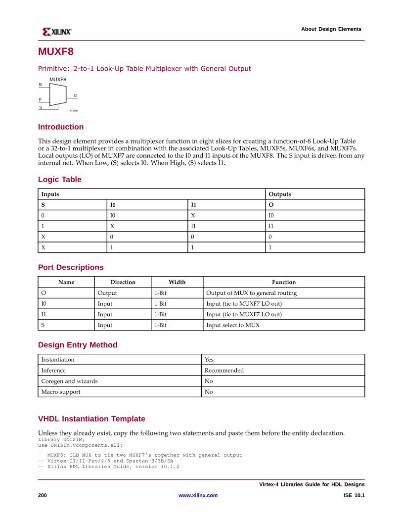
About Design Elements
MUXF8
Primitive: 2-to-1 Look-Up Table Multiplexer with General Output
Intr oduction
This design element provides a multiplexer function in eight slices for creating a function-of-8 Look-Up Tableor a 32-to-1 multiplexer in combination with the associated Look-Up Tables, MUXF5s, MUXF6s, and MUXF7s.Local outputs (LO) of MUXF7 are connected to the I0 and I1 inputs of the MUXF8. The S input is driven from anyinternal net. When Low, (S) selects I0. When High, (S) selects I1.
Logic Table
Inputs Outputs
S I0 I1 O
0 I0 X I0
1 X I1 I1
X 0 0 0
X 1 1 1
Por t Descriptions
Name Direction Width Function
O Output 1-Bit Output of MUX to general routing
I0 Input 1-Bit Input (tie to MUXF7 LO out)
I1 Input 1-Bit Input (tie to MUXF7 LO out)
S Input 1-Bit Input select to MUX
Design Entr y Method
Instantiation Yes
Inference Recommended
Coregen and wizards No
Macro support No
VHDL Instantiation Template
Unless they already exist, copy the following two statements and paste them before the entity declaration.Library UNISIM;use UNISIM.vcomponents.all;
-- MUXF8: CLB MUX to tie two MUXF7’s together with general output-- Virtex-II/II-Pro/4/5 and Spartan-3/3E/3A-- Xilinx HDL Libraries Guide, version 10.1.2
Vir tex-4 Libraries Guide for HDL Designs
200 www.xilinx.com ISE 10.1
About Design Elements
MUXF8_inst : MUXF8port map (O => O, -- Output of MUX to general routingI0 => I0, -- Input (tie to MUXF7 LO out)I1 => I1, -- Input (tie to MUXF7 LO out)S => S -- Input select to MUX);
-- End of MUXF8_inst instantiation
Verilog Instantiation Template
// MUXF8: CLB MUX to tie two MUXF7’s together with general output// For use with Virtex-II/II-Pro/4/5 and Spartan-3/3E/3A// Xilinx HDL Libraries Guide, version 10.1.2
MUXF8MUXF8_inst (.O(O), // Output of MUX to general routing.I0(I0), // Input (tie to MUXF7 LO out).I1(I1), // Input (tie to MUXF7 LO out).S(S) // Input select to MUX);
// End of MUXF8_inst instantiation
For More Information
• See the Virtex-4 User Guide.
• See the Virtex-4 Data Sheets.
Vir tex-4 Libraries Guide for HDL Designs
ISE 10.1 www.xilinx.com 201
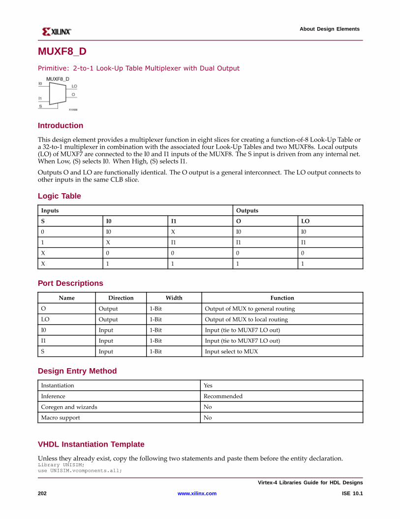
About Design Elements
MUXF8_D
Primitive: 2-to-1 Look-Up Table Multiplexer with Dual Output
Intr oduction
This design element provides a multiplexer function in eight slices for creating a function-of-8 Look-Up Table ora 32-to-1 multiplexer in combination with the associated four Look-Up Tables and two MUXF8s. Local outputs(LO) of MUXF7 are connected to the I0 and I1 inputs of the MUXF8. The S input is driven from any internal net.When Low, (S) selects I0. When High, (S) selects I1.
Outputs O and LO are functionally identical. The O output is a general interconnect. The LO output connects toother inputs in the same CLB slice.
Logic Table
Inputs Outputs
S I0 I1 O LO
0 I0 X I0 I0
1 X I1 I1 I1
X 0 0 0 0
X 1 1 1 1
Por t Descriptions
Name Direction Width Function
O Output 1-Bit Output of MUX to general routing
LO Output 1-Bit Output of MUX to local routing
I0 Input 1-Bit Input (tie to MUXF7 LO out)
I1 Input 1-Bit Input (tie to MUXF7 LO out)
S Input 1-Bit Input select to MUX
Design Entr y Method
Instantiation Yes
Inference Recommended
Coregen and wizards No
Macro support No
VHDL Instantiation Template
Unless they already exist, copy the following two statements and paste them before the entity declaration.Library UNISIM;use UNISIM.vcomponents.all;
Vir tex-4 Libraries Guide for HDL Designs
202 www.xilinx.com ISE 10.1

About Design Elements
-- MUXF8_D: CLB MUX to tie two MUXF7’s together with general and local outputs-- Virtex-II/II-Pro/4/5 and Spartan-3/3E/3A-- Xilinx HDL Libraries Guide, version 10.1.2
MUXF8_D_inst : MUXF8_Dport map (LO => LO, -- Ouptut of MUX to local routingO => O, -- Output of MUX to general routingI0 => I0, -- Input (tie to MUXF7 LO out)I1 => I1, -- Input (tie to MUXF7 LO out)S => S -- Input select to MUX);
-- End of MUXF8_D_inst instantiation
Verilog Instantiation Template
// MUXF8_D: CLB MUX to tie two MUXF7’s together with general and local outputs// For use with Virtex-II/II-Pro/4/5 and Spartan-3/3E/3A// Xilinx HDL Libraries Guide, version 10.1.2
MUXF8_DMUXF8_D_inst (.LO(LO), // Ouptut of MUX to local routing.O(O), // Output of MUX to general routing.I0(I0), // Input (tie to MUXF7 LO out).I1(I1), // Input (tie to MUXF7 LO out).S(S) // Input select to MUX);
// End of MUXF8_D_inst instantiation
For More Information
• See the Virtex-4 User Guide.
• See the Virtex-4 Data Sheets.
Vir tex-4 Libraries Guide for HDL Designs
ISE 10.1 www.xilinx.com 203
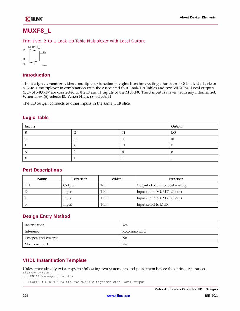
About Design Elements
MUXF8_L
Primitive: 2-to-1 Look-Up Table Multiplexer with Local Output
Intr oduction
This design element provides a multiplexer function in eight slices for creating a function-of-8 Look-Up Table ora 32-to-1 multiplexer in combination with the associated four Look-Up Tables and two MUXF8s. Local outputs(LO) of MUXF7 are connected to the I0 and I1 inputs of the MUXF8. The S input is driven from any internal net.When Low, (S) selects I0. When High, (S) selects I1.
The LO output connects to other inputs in the same CLB slice.
Logic Table
Inputs Output
S I0 I1 LO
0 I0 X I0
1 X I1 I1
X 0 0 0
X 1 1 1
Por t Descriptions
Name Direction Width Function
LO Output 1-Bit Output of MUX to local routing
I0 Input 1-Bit Input (tie to MUXF7 LO out)
I1 Input 1-Bit Input (tie to MUXF7 LO out)
S Input 1-Bit Input select to MUX
Design Entr y Method
Instantiation Yes
Inference Recommended
Coregen and wizards No
Macro support No
VHDL Instantiation Template
Unless they already exist, copy the following two statements and paste them before the entity declaration.Library UNISIM;use UNISIM.vcomponents.all;
-- MUXF8_L: CLB MUX to tie two MUXF7’s together with local output
Vir tex-4 Libraries Guide for HDL Designs
204 www.xilinx.com ISE 10.1

About Design Elements
-- Virtex-II/II-Pro/4/5 and Spartan-3/3E/3A-- Xilinx HDL Libraries Guide, version 10.1.2
MUXF8_L_inst : MUXF8_Lport map (LO => LO, -- Output of MUX to local routingI0 => I0, -- Input (tie to MUXF7 LO out)I1 => I1, -- Input (tie to MUXF7 LO out)S => S -- Input select to MUX);
-- End of MUXF8_L_inst instantiation
Verilog Instantiation Template
// MUXF8_L: CLB MUX to tie two MUXF7’s together with local output// For use with Virtex-II/II-Pro/4/5 and Spartan-3/3E/3A// Xilinx HDL Libraries Guide, version 10.1.2
MUXF8_L MUXF8_L_inst (.LO(LO), // Output of MUX to local routing.I0(I0), // Input (tie to MUXF7 LO out).I1(I1), // Input (tie to MUXF7 LO out).S(S) // Input select to MUX);
// End of MUXF8_L_inst instantiation
For More Information
• See the Virtex-4 User Guide.
• See the Virtex-4 Data Sheets.
Vir tex-4 Libraries Guide for HDL Designs
ISE 10.1 www.xilinx.com 205
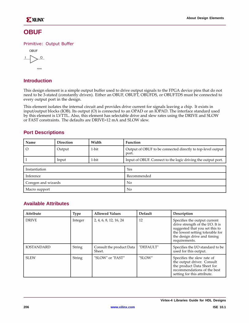
About Design Elements
OBUF
Primitive: Output Buffer
Intr oduction
This design element is a simple output buffer used to drive output signals to the FPGA device pins that do notneed to be 3-stated (constantly driven). Either an OBUF, OBUFT, OBUFDS, or OBUFTDS must be connected toevery output port in the design.
This element isolates the internal circuit and provides drive current for signals leaving a chip. It exists ininput/output blocks (IOB). Its output (O) is connected to an OPAD or an IOPAD. The interface standard usedby this element is LVTTL. Also, this element has selectable drive and slew rates using the DRIVE and SLOWor FAST constraints. The defaults are DRIVE=12 mA and SLOW slew.
Por t Descriptions
Name Direction Width Function
O Output 1-bit Output of OBUF to be connected directly to top-level outputport.
I Input 1-bit Input of OBUF. Connect to the logic driving the output port.
Instantiation Yes
Inference Recommended
Coregen and wizards No
Macro support No
Availab le Attrib utes
Attribute Type Allowed Values Default Description
DRIVE Integer 2, 4, 6, 8, 12, 16, 24 12 Specifies the output currentdrive strength of the I/O. It issuggested that you set this tothe lowest setting tolerable forthe design drive and timingrequirements.
IOSTANDARD String Consult the product DataSheet.
"DEFAULT" Specifies the I/O standard to beused for this output.
SLEW String "SLOW" or "FAST” "SLOW” Specifies the slew rate ofthe output driver. Consultthe product Data Sheet forrecommendations of the bestsetting for this attribute.
Vir tex-4 Libraries Guide for HDL Designs
206 www.xilinx.com ISE 10.1
About Design Elements
VHDL Instantiation Template
Unless they already exist, copy the following two statements and paste them before the entity declaration.Library UNISIM;use UNISIM.vcomponents.all;
-- OBUF: Single-ended Output Buffer-- All devices-- Xilinx HDL Libraries Guide, version 10.1.2
OBUF_inst : OBUFgeneric map (DRIVE => 12,IOSTANDARD=> "DEFAULT",SLEW=> "SLOW")port map (O => O, -- Buffer output (connect directly to top-level port)I => I -- Buffer input);
-- End of OBUF_inst instantiation
Verilog Instantiation Template
// OBUF: Single-ended Output Buffer// All devices// Xilinx HDL Libraries Guide, version 10.1.2
OBUF #(.DRIVE(12), // Specify the output drive strength.IOSTANDARD("DEFAULT"), // Specify the output I/O standard.SLEW("SLOW") // Specify the output slew rate) OBUF_inst (.O(O), // Buffer output (connect directly to top-level port).I(I) // Buffer input);
// End of OBUF_inst instantiation
For More Information
• See the Virtex-4 User Guide.
• See the Virtex-4 Data Sheets.
Vir tex-4 Libraries Guide for HDL Designs
ISE 10.1 www.xilinx.com 207
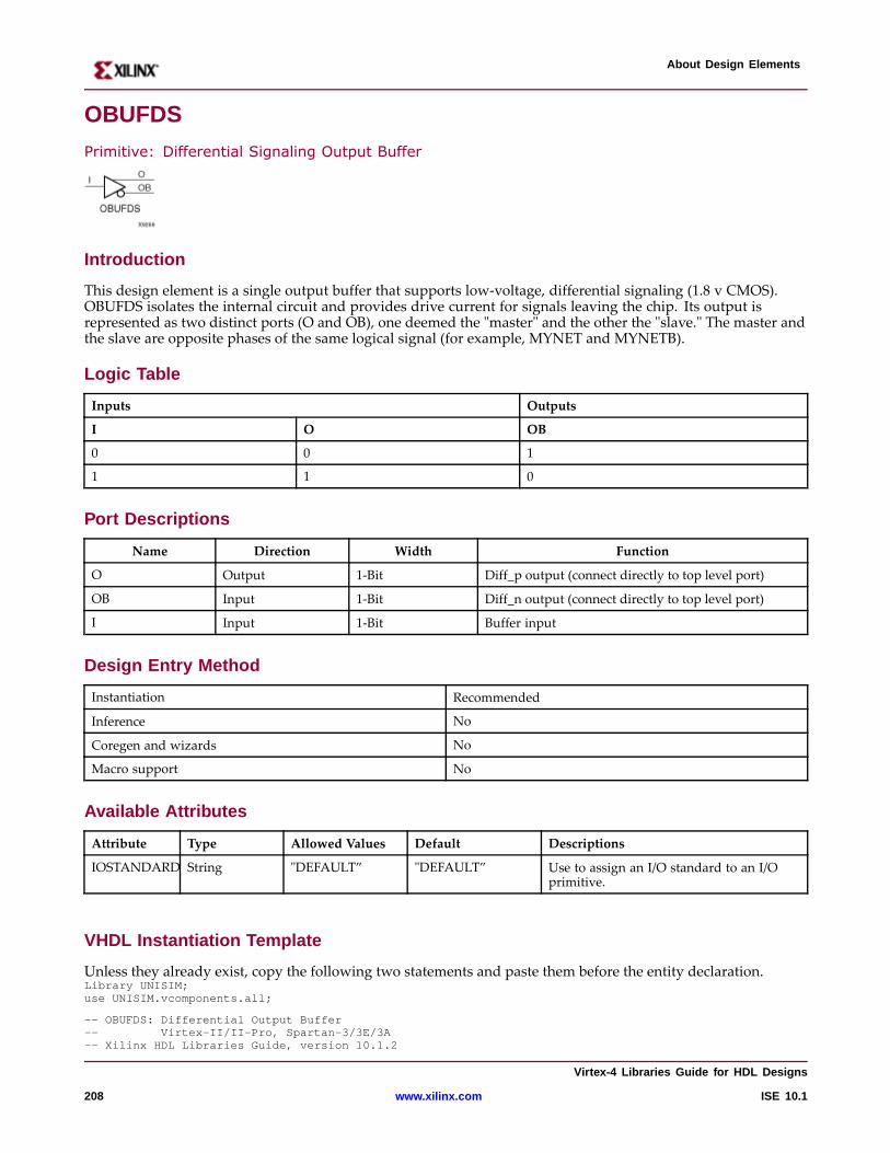
About Design Elements
OBUFDS
Primitive: Differential Signaling Output Buffer
Intr oduction
This design element is a single output buffer that supports low-voltage, differential signaling (1.8 v CMOS).OBUFDS isolates the internal circuit and provides drive current for signals leaving the chip. Its output isrepresented as two distinct ports (O and OB), one deemed the "master" and the other the "slave." The master andthe slave are opposite phases of the same logical signal (for example, MYNET and MYNETB).
Logic Table
Inputs Outputs
I O OB
0 0 1
1 1 0
Por t Descriptions
Name Direction Width Function
O Output 1-Bit Diff_p output (connect directly to top level port)
OB Input 1-Bit Diff_n output (connect directly to top level port)
I Input 1-Bit Buffer input
Design Entr y Method
Instantiation Recommended
Inference No
Coregen and wizards No
Macro support No
Availab le Attrib utes
Attribute Type Allowed Values Default Descriptions
IOSTANDARD String "DEFAULT” "DEFAULT” Use to assign an I/O standard to an I/Oprimitive.
VHDL Instantiation Template
Unless they already exist, copy the following two statements and paste them before the entity declaration.Library UNISIM;use UNISIM.vcomponents.all;
-- OBUFDS: Differential Output Buffer-- Virtex-II/II-Pro, Spartan-3/3E/3A-- Xilinx HDL Libraries Guide, version 10.1.2
Vir tex-4 Libraries Guide for HDL Designs
208 www.xilinx.com ISE 10.1
About Design Elements
OBUFDS_inst : OBUFDSgeneric map (IOSTANDARD=> "DEFAULT")port map (O => O, -- Diff_p output (connect directly to top-level port)OB => OB, -- Diff_n output (connect directly to top-level port)I => I -- Buffer input);
-- End of OBUFDS_inst instantiation
Verilog Instantiation Template
// OBUFDS: Differential Output Buffer// Virtex-II/II-Pro/4/5, Spartan-3/3E/3A// Xilinx HDL Libraries Guide, version 10.1.2
OBUFDS#(.IOSTANDARD("DEFAULT") // Specify the output I/O standard) OBUFDS_inst (.O(O), // Diff_p output (connect directly to top-level port).OB(OB), // Diff_n output (connect directly to top-level port).I(I) // Buffer input);
// End of OBUFDS_inst instantiation
For More Information
• See the Virtex-4 User Guide.
• See the Virtex-4 Data Sheets.
Vir tex-4 Libraries Guide for HDL Designs
ISE 10.1 www.xilinx.com 209
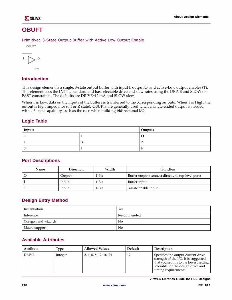
About Design Elements
OBUFT
Primitive: 3-State Output Buffer with Active Low Output Enable
Intr oduction
This design element is a single, 3-state output buffer with input I, output O, and active-Low output enables (T).This element uses the LVTTL standard and has selectable drive and slew rates using the DRIVE and SLOW orFAST constraints. The defaults are DRIVE=12 mA and SLOW slew.
When T is Low, data on the inputs of the buffers is transferred to the corresponding outputs. When T is High, theoutput is high impedance (off or Z state). OBUFTs are generally used when a single-ended output is neededwith a 3-state capability, such as the case when building bidirectional I/O.
Logic Table
Inputs Outputs
T I O
1 X Z
0 I F
Por t Descriptions
Name Direction Width Function
O Output 1-Bit Buffer output (connect directly to top-level port)
I Input 1-Bit Buffer input
T Input 1-Bit 3-state enable input
Design Entr y Method
Instantiation Yes
Inference Recommended
Coregen and wizards No
Macro support No
Availab le Attrib utes
Attribute Type Allowed Values Default Description
DRIVE Integer 2, 4, 6, 8, 12, 16, 24 12 Specifies the output current drivestrength of the I/O. It is suggestedthat you set this to the lowest settingtolerable for the design drive andtiming requirements.
Vir tex-4 Libraries Guide for HDL Designs
210 www.xilinx.com ISE 10.1
About Design Elements
Attribute Type Allowed Values Default Description
IOSTANDARD String Consult the product DataSheet.
"DEFAULT" Specifies the I/O standard to be usedfor this output.
SLEW String "SLOW" or "FAST” "SLOW” Specifies the slew rate of the outputdriver. Consult the product DataSheet for recommendations of thebest setting for this attribute.
VHDL Instantiation Template
Unless they already exist, copy the following two statements and paste them before the entity declaration.Library UNISIM;use UNISIM.vcomponents.all;
-- OBUFT: Single-ended 3-state Output Buffer-- All devices-- Xilinx HDL Libraries Guide, version 10.1.2
OBUFT_inst : OBUFTgeneric map (DRIVE => 12,IOSTANDARD=> "DEFAULT",SLEW=> "SLOW")port map (O => O, -- Buffer output (connect directly to top-level port)I => I, -- Buffer inputT => T -- 3-state enable input);
-- End of OBUFT_inst instantiation
Verilog Instantiation Template
// OBUFT: Single-ended 3-state Output Buffer// All devices// Xilinx HDL Libraries Guide, version 10.1.2
OBUFT #(.DRIVE(12), // Specify the output drive strength.IOSTANDARD("DEFAULT"), // Specify the output I/O standard.SLEW("SLOW") // Specify the output slew rate) OBUFT_inst (.O(O), // Buffer output (connect directly to top-level port).I(I), // Buffer input.T(T) // 3-state enable input);
// End of OBUFT_inst instantiation
For More Information
• See the Virtex-4 User Guide.
• See the Virtex-4 Data Sheets.
Vir tex-4 Libraries Guide for HDL Designs
ISE 10.1 www.xilinx.com 211
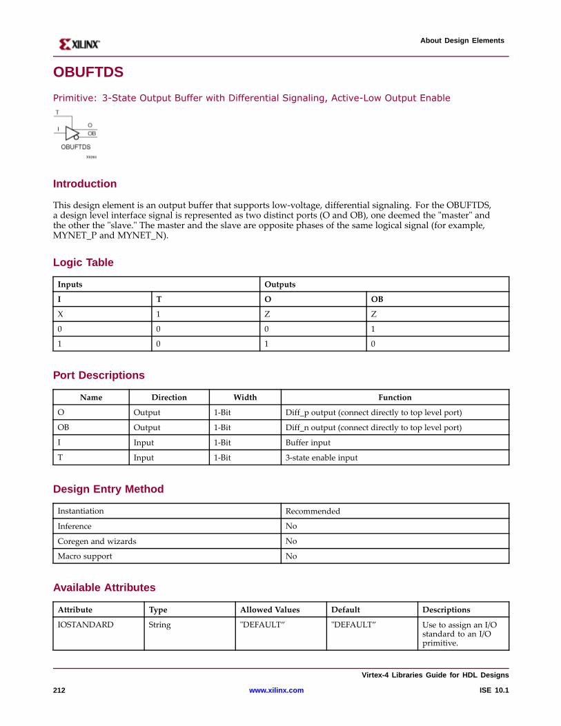
About Design Elements
OBUFTDS
Primitive: 3-State Output Buffer with Differential Signaling, Active-Low Output Enable
Intr oduction
This design element is an output buffer that supports low-voltage, differential signaling. For the OBUFTDS,a design level interface signal is represented as two distinct ports (O and OB), one deemed the "master" andthe other the "slave." The master and the slave are opposite phases of the same logical signal (for example,MYNET_P and MYNET_N).
Logic Table
Inputs Outputs
I T O OB
X 1 Z Z
0 0 0 1
1 0 1 0
Por t Descriptions
Name Direction Width Function
O Output 1-Bit Diff_p output (connect directly to top level port)
OB Output 1-Bit Diff_n output (connect directly to top level port)
I Input 1-Bit Buffer input
T Input 1-Bit 3-state enable input
Design Entr y Method
Instantiation Recommended
Inference No
Coregen and wizards No
Macro support No
Availab le Attrib utes
Attribute Type Allowed Values Default Descriptions
IOSTANDARD String "DEFAULT” "DEFAULT” Use to assign an I/Ostandard to an I/Oprimitive.
Vir tex-4 Libraries Guide for HDL Designs
212 www.xilinx.com ISE 10.1
About Design Elements
VHDL Instantiation Template
Unless they already exist, copy the following two statements and paste them before the entity declaration.Library UNISIM;use UNISIM.vcomponents.all;
-- OBUFTDS: Differential 3-state Output Buffer-- Virtex-II/II-Pro, Spartan-3/3E/3A-- Xilinx HDL Libraries Guide, version 10.1.2
OBUFTDS_inst : OBUFTDSgeneric map (IOSTANDARD=> "DEFAULT")port map (O => O, -- Diff_p output (connect directly to top-level port)OB => OB, -- Diff_n output (connect directly to top-level port)I => I, -- Buffer inputT => T -- 3-state enable input);
-- End of OBUFTDS_inst instantiation
Verilog Instantiation Template
// OBUFTDS: Differential 3-state Output Buffer// Virtex-II/II-Pro/4/5, Spartan-3/3E/3A// Xilinx HDL Libraries Guide, version 10.1.2
OBUFTDS#(.IOSTANDARD("DEFAULT") // Specify the output I/O standard) OBUFTDS_inst (.O(O), // Diff_p output (connect directly to top-level port).OB(OB), // Diff_n output (connect directly to top-level port).I(I), // Buffer input.T(T) // 3-state enable input);
// End of OBUFTDS_inst instantiation
For More Information
• See the Virtex-4 User Guide.
• See the Virtex-4 Data Sheets.
Vir tex-4 Libraries Guide for HDL Designs
ISE 10.1 www.xilinx.com 213
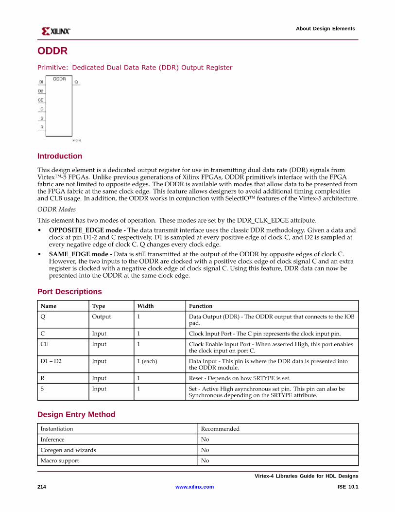
About Design Elements
ODDR
Primitive: Dedicated Dual Data Rate (DDR) Output Register
Intr oduction
This design element is a dedicated output register for use in transmitting dual data rate (DDR) signals fromVirtex™-5 FPGAs. Unlike previous generations of Xilinx FPGAs, ODDR primitive’s interface with the FPGAfabric are not limited to opposite edges. The ODDR is available with modes that allow data to be presented fromthe FPGA fabric at the same clock edge. This feature allows designers to avoid additional timing complexitiesand CLB usage. In addition, the ODDRworks in conjunction with SelectIO™ features of the Virtex-5 architecture.
ODDR Modes
This element has two modes of operation. These modes are set by the DDR_CLK_EDGE attribute.• OPPOSITE_EDGE mode - The data transmit interface uses the classic DDR methodology. Given a data and
clock at pin D1-2 and C respectively, D1 is sampled at every positive edge of clock C, and D2 is sampled atevery negative edge of clock C. Q changes every clock edge.
• SAME_EDGE mode - Data is still transmitted at the output of the ODDR by opposite edges of clock C.However, the two inputs to the ODDR are clocked with a positive clock edge of clock signal C and an extraregister is clocked with a negative clock edge of clock signal C. Using this feature, DDR data can now bepresented into the ODDR at the same clock edge.
Por t Descriptions
Name Type Width Function
Q Output 1 Data Output (DDR) - The ODDR output that connects to the IOBpad.
C Input 1 Clock Input Port - The C pin represents the clock input pin.
CE Input 1 Clock Enable Input Port - When asserted High, this port enablesthe clock input on port C.
D1 – D2 Input 1 (each) Data Input - This pin is where the DDR data is presented intothe ODDR module.
R Input 1 Reset - Depends on how SRTYPE is set.
S Input 1 Set - Active High asynchronous set pin. This pin can also beSynchronous depending on the SRTYPE attribute.
Design Entr y Method
Instantiation Recommended
Inference No
Coregen and wizards No
Macro support No
Vir tex-4 Libraries Guide for HDL Designs
214 www.xilinx.com ISE 10.1
About Design Elements
Availab le Attrib utes
Attribute Type Allowed Values Default Description
DDR_CLK_EDGE
String "OPPOSITE_EDGE","SAME_EDGE"
"OPPOSITE_ EDGE" DDR clock mode recovery modeselection.
INIT Integer 0 or 1 1 Q initialization value.
SRTYPE String "SYNC" or "ASYNC" "SYNC" Set/Reset type selection.
VHDL Instantiation Template
Unless they already exist, copy the following two statements and paste them before the entity declaration.Library UNISIM;use UNISIM.vcomponents.all;
-- ODDR: Output Double Data Rate Output Register with Set, Reset-- and Clock Enable.-- Virtex-4/5-- Xilinx HDL Libraries Guide, version 10.1.2
ODDR_inst : ODDRgeneric map(DDR_CLK_EDGE=> "OPPOSITE_EDGE", -- "OPPOSITE_EDGE" or "SAME_EDGE"INIT => ’0’, -- Initial value for Q port (’1’ or ’0’)SRTYPE => "SYNC") -- Reset Type ("ASYNC" or "SYNC")port map (Q => Q, -- 1-bit DDR outputC => C, -- 1-bit clock inputCE => CE, -- 1-bit clock enable inputD1 => D1, -- 1-bit data input (positive edge)D2 => D2, -- 1-bit data input (negative edge)R => R, -- 1-bit reset inputS => S -- 1-bit set input);
-- End of ODDR_inst instantiation
Verilog Instantiation Template
// ODDR: Output Double Data Rate Output Register with Set, Reset// and Clock Enable.// Virtex-4/5// Xilinx HDL Libraries Guide, version 10.1.2
ODDR#(.DDR_CLK_EDGE("OPPOSITE_EDGE"), // "OPPOSITE_EDGE" or "SAME_EDGE".INIT(1’b0), // Initial value of Q: 1’b0 or 1’b1.SRTYPE("SYNC") // Set/Reset type: "SYNC" or "ASYNC") ODDR_inst (.Q(Q), // 1-bit DDR output.C(C), // 1-bit clock input.CE(CE), // 1-bit clock enable input.D1(D1), // 1-bit data input (positive edge).D2(D2), // 1-bit data input (negative edge).R(R), // 1-bit reset.S(S) // 1-bit set);
// End of ODDR_inst instantiation
Vir tex-4 Libraries Guide for HDL Designs
ISE 10.1 www.xilinx.com 215

About Design Elements
For More Information
• See the Virtex-4 User Guide.
• See the Virtex-4 Data Sheets.
Vir tex-4 Libraries Guide for HDL Designs
216 www.xilinx.com ISE 10.1
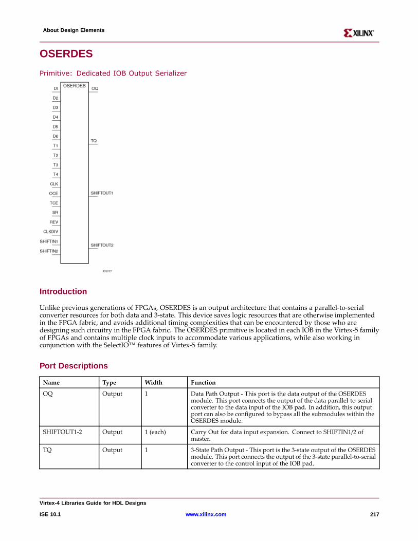
About Design Elements
OSERDES
Primitive: Dedicated IOB Output Serializer
Intr oduction
Unlike previous generations of FPGAs, OSERDES is an output architecture that contains a parallel-to-serialconverter resources for both data and 3-state. This device saves logic resources that are otherwise implementedin the FPGA fabric, and avoids additional timing complexities that can be encountered by those who aredesigning such circuitry in the FPGA fabric. The OSERDES primitive is located in each IOB in the Virtex-5 familyof FPGAs and contains multiple clock inputs to accommodate various applications, while also working inconjunction with the SelectIO™ features of Virtex-5 family.
Por t Descriptions
Name Type Width Function
OQ Output 1 Data Path Output - This port is the data output of the OSERDESmodule. This port connects the output of the data parallel-to-serialconverter to the data input of the IOB pad. In addition, this outputport can also be configured to bypass all the submodules within theOSERDES module.
SHIFTOUT1-2 Output 1 (each) Carry Out for data input expansion. Connect to SHIFTIN1/2 ofmaster.
TQ Output 1 3-State Path Output - This port is the 3-state output of the OSERDESmodule. This port connects the output of the 3-state parallel-to-serialconverter to the control input of the IOB pad.
Vir tex-4 Libraries Guide for HDL Designs
ISE 10.1 www.xilinx.com 217
About Design Elements
Name Type Width Function
CLK Input 1 High Speed Clock Input - This clock input is used to drive theparallel-to-serial converters. The possible source for the CLK port isfrom one of the following clock resources:
1. Ten global clock lines in a clock region
2. Four regional clock lines
3. Four clock capable I/Os (within adjacent clock region)
4. Fabric (through bypass)
CLKDIV Input 1 Divided High Speed Clock Input - This clock input is used to drivethe parallel-to-serial converter. This clock must be a divided downversion of the clock connected to the CLK port. One of the followingclock resources can be used as a source for CLKDIV:
1. Ten global clock lines in a clock region
2. Four regional clock lines
D1-D6 Input 1 Parallel Data Inputs - Ports D1 to D6 are the location in which allincoming parallel data enters the OSERDES module. This port isconnected to the FPGA fabric, and can be configured from 2 to 6 bits.In the extended width mode, this port can be expanded up to 10 bits.
OCE Input 1 Parallel to serial converter (data) clock enable - This port is usedto enables the output of the data parallel-to-serial converter whenasserted High.
SR Input 1 Set/Reset Input - The set/reset (SR) pin forces the storage elementinto the state specified by the SRVAL attribute. SRVAL = “1”forces a logic 1. SRVAL = “0” forces a logic "0." The reset conditionpredominates over the set condition.
SHIFTIN1-2 Input 1 (each) Carry Input for Data Input Expansion. Connect to SHIFTOUT1/2of slave.
T1 – T4 Input 1 (each) Parallel 3-State Inputs - Ports T1 to T4 are the location in which allparallel 3-state signals enters the OSERDES module. This port isconnected to the FPGA fabric, and can be configured from 1 to 4 bits.This feature is not supported in the extended width mode.
TCE Input 1 Parallel to serial converter (3-state) clock enable - This port is usedto enable the output of the 3-state signal parallel-to-serial converterwhen asserted High.
Design Entr y Method
Instantiation Recommended
Inference No
Coregen and wizards No
Macro support No
The data parallel-to-serial converter in the OSERDES module takes in 2 to 6 bits of parallel data and convertsthem into serial data. Data input widths larger than 6 (7, 8, and 10) are achievable by cascading two OSERDESmodules for data width expansion. In order to do this, one OSERDES must be set into a MASTER mode, whileanother is set into SLAVE mode. You must connect the SHIFTOUT of "slave" and SHIFTIN of "master" portstogether. The "slave" only uses D3 to D6 ports as its input. The parallel-to-serial converter is available for bothSDR and DDR modes.
This module is designed such that the data input at D1 port is the first output bit. This module is controlledby CLK and CLKDIV clocks. The following table describes the relationship between CLK and CLKDIV forboth SDR and DDR mode.
Vir tex-4 Libraries Guide for HDL Designs
218 www.xilinx.com ISE 10.1
About Design Elements
SDR Data Width DDR Data Width CLK CLKDIV
2 4 2X X
3 6 3X X
4 8 4X X
5 10 5X X
6 - 6X X
7 - 7X X
8 - 8X X
Output of this block is connected to the data input of an IOB pad of the FPGA. This IOB pad can be configured toa desired standard using SelectIO.
Parallel-to-Serial Converter (3-state)
The 3-state parallel-to-serial converter in the OSERDES module takes in up to 4 bits of parallel 3-state signals andconverts them into serial 3-state signal. Unlike the data parallel-to-serial converter, the 3-state parallel-to-serialconverter is not extendable to more than 4-bit, 3-state signals. This module is primarily controlled by CLK andCLKDIV clocks. In order to use this module, the following attributes must be declared: DATA_RATE_TQ andTRISTATE_WIDTH. In certain cases, you can also need to declare DATA_RATE_OQ and DATA_WIDTH. Thefollowing table lists the attributes needed for the desired functionality.
Mode of Operation DATA_RATE_TQ TRISTATE_WIDTH
4-bit DDR* DDR 4
1-bit SDR SDR 1
Buffer BUF 1
Output of this block is connected to the 3-state input of an IOB pad of the FPGA. This IOB pad can be configuredto a desired standard using SelectIO.
Width Expansion
It is possible to use this element to transmit parallel data widths larger than six. However, the 3-state output isnot expandable. In order to use this feature, two of these elements need to be instantiated, and the two must be anadjacent master and slave pair. The attribute MODE must be set to either "MASTER" or "SLAVE" in order todifferentiate the modes of the OSERDES pair. In addition, you must connect the SHIFTIN ports of the MASTERto the SHIFTOUT ports of the SLAVE. This feature supports data widths of 7, 8, and 10 for SDR and DDR mode.The table below lists the data width availability for SDR and DDR mode.
Mode Widths
SDR Data Widths 2,3,4,5,6,7,8
DDR Data Widths 4,6,8,10
Availab le Attrib utes
Attribute Type Allowed Values Default Description
DATA_RATE_OQ String "SDR" or"DDR"
"DDR" Defines whether the data changes at everyclock edge or every positive clock edgewith respect to CLK.
DATA_RATE_TQ String "BUF", "SDR","DDR"
"DDR" Defines whether the 3-state changes atevery clock edge, every positive clockedge, or buffer configuration with respectto CLK.
Vir tex-4 Libraries Guide for HDL Designs
ISE 10.1 www.xilinx.com 219
About Design Elements
Attribute Type Allowed Values Default Description
DATA_WIDTH Integer 2, 3, 4, 5, 6, 7, 8, or 10 4 If DATA_RATE_OQ = DDR, valueis limited to 4, 6, 8, or 10. IfDATA_RATE_OQ = SDR, value islimited to 2, 3, 4, 5, 6, 7, or 8.
INIT_OQ Binary 0, 1 0 Defines the initial value of OQ output
INIT_TQ Binary 0, 1 0 Defines the initial value of TQ output
SERDES_MODE String "MASTER or"SLAVE"
"MASTER" Defines whether the OSERDES module isa master or slave when width expansionis used.
SRVAL_OQ Binary 0, 1 0 Defines the value of OQ output whenreset is invoked.
SRVAL_TQ Binary 0, 1 0 Defines the value of TQ output whenreset is invoked.
TRISTATE_WIDTH Integer 1 or 4 4 If DATA_RATE_TQ = DDR,DATA_WIDTH= 4, andDATA_RATE_OQ= DDR, value is limited to 1 or 4. Forall other settings of DATA_RATE_TQ,DATA_WIDTH, and DATA_RATE_OQ,value is limited to 1.
VHDL Instantiation Template
Unless they already exist, copy the following two statements and paste them before the entity declaration.Library UNISIM;use UNISIM.vcomponents.all;
-- OSERDES: Output SERDES-- Virtex-4-- Xilinx HDL Libraries Guide, version 10.1.2
OSERDES_inst : OSERDESgeneric map (DATA_RATE_OQ=> "DDR", -- Specify data rate to "DDR" or "SDR"DATA_RATE_TQ=> "DDR", -- Specify data rate to "DDR", "SDR", or "BUF"DATA_WIDTH=> 4, -- Specify data width - For DDR: 4,6,8, or 10-- For SDR or BUF: 2,3,4,5,6,7, or 8INIT_OQ => ’0’, -- INIT for Q1 register - ’1’ or ’0’INIT_TQ => ’0’, -- INIT for Q2 register - ’1’ or ’0’SERDES_MODE=> "MASTER", --Set SERDESmode to "MASTER" or "SLAVE"SRVAL_OQ=> ’0’, -- Define Q1 output value upon SR assertion - ’1’ or ’0’SRVAL_TQ=> ’0’, -- Define Q1 output value upon SR assertion - ’1’ or ’0’TRISTATE_WIDTH => 4) -- Specify parallel to serial converter width-- When DATA_RATE_TQ= DDR: 2 or 4-- When DATA_RATE_TQ= SDR or BUF: 1 "port map (OQ => OQ, -- 1-bit outputSHIFTOUT1 => SHIFTOUT1, -- 1-bit data expansion outputSHIFTOUT2 => SHIFTOUT2, -- 1-bit data expansion outputTQ => TQ, -- 1-bit 3-state control outputCLK => CLK, -- 1-bit clock inputCLKDIV => CLKDIV, -- 1-bit divided clock inputD1 => D1, -- 1-bit parallel data inputD2 => D2, -- 1-bit parallel data inputD3 => D3, -- 1-bit parallel data inputD4 => D4, -- 1-bit parallel data inputD5 => D5, -- 1-bit parallel data inputD6 => D6, -- 1-bit parallel data inputOCE => OCE, -- 1-bit clcok enable inputREV => ’0’, -- Must be tied to logic zeroSHIFTIN1 => SHIFTIN1, -- 1-bit data expansion inputSHIFTIN2 => SHIFTIN2, -- 1-bit data expansion inputSR => SR, -- 1-bit set/reset input
Vir tex-4 Libraries Guide for HDL Designs
220 www.xilinx.com ISE 10.1
About Design Elements
T1 => T1, -- 1-bit parallel 3-state inputT2 => T2, -- 1-bit parallel 3-state inputT3 => T3, -- 1-bit parallel 3-state inputT4 => T4, -- 1-bit parallel 3-state inputTCE => TCE -- 1-bit 3-state signal clock enable input);
-- End of OSERDES_inst instantiation
Verilog Instantiation Template
// OSERDES: Source Synchronous Output Serializer// Virtex-4/5// Xilinx HDL Libraries Guide, version 10.1.2
OSERDES#(.DATA_RATE_OQ("DDR"), // Specify data rate to "DDR" or "SDR".DATA_RATE_TQ("DDR"), // Specify data rate to "DDR", "SDR", or "BUF".DATA_WIDTH(4), // Specify data width - For DDR: 4,6,8, or 10// For SDR or BUF: 2,3,4,5,6,7, or 8.INIT_OQ(1’b0), // INIT for OQ register - 1’b1 or 1’b0.INIT_TQ(1’b0), // INIT for OQ register - 1’b1 or 1’b0.SERDES_MODE("MASTER"), // Set SERDESmode to "MASTER" or "SLAVE".SRVAL_OQ(1’b0), // Define OQ output value upon SR assertion - 1’b1 or 1’b0.SRVAL_TQ(1’b0), // Define TQ output value upon SR assertion - 1’b1 or 1’b0.TRISTATE_WIDTH(4) // Specify parallel to serial converter width// When DATA_RATE_TQ= DDR: 2 or 4// When DATA_RATE_TQ= SDR or BUF: 1) OSERDES_inst (.OQ(OQ), // 1-bit data path output.SHIFTOUT1(SHIFTOUT1), // 1-bit data expansion output.SHIFTOUT2(SHIFTOUT2), // 1-bit data expansion output.TQ(TQ), // 1-bit 3-state control output.CLK(CLK), // 1-bit clock input.CLKDIV(CLKDIV), // 1-bit divided clock input.D1(D1), // 1-bit parallel data input.D2(D2), // 1-bit parallel data input.D3(D3), // 1-bit parallel data input.D4(D4), // 1-bit parallel data input.D5(D5), // 1-bit parallel data input.D6(D6), // 1-bit parallel data input.OCE(OCE), // 1-bit clock enable input.REV(1’b0), // Must be tied to logic zero.SHIFTIN1(SHIFTIN1), // 1-bit data expansion input.SHIFTIN2(SHIFTIN2), // 1-bit data expansion input.SR(SR), // 1-bit set/reset input.T1(T1), // 1-bit parallel 3-state input.T2(T2), // 1-bit parallel 3-state input.T3(T3), // 1-bit parallel 3-state input.T4(T4), // 1-bit parallel 3-state input.TCE(TCE) // 1-bit 3-state signal clock enable input);
// End of OSERDES_inst instantiation
For More Information
• See the Virtex-4 User Guide.
• See the Virtex-4 Data Sheets.
Vir tex-4 Libraries Guide for HDL Designs
ISE 10.1 www.xilinx.com 221
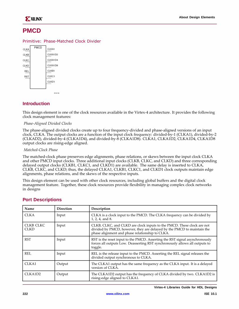
About Design Elements
PMCD
Primitive: Phase-Matched Clock Divider
Intr oduction
This design element is one of the clock resources available in the Virtex-4 architecture. It provides the followingclock management features:
Phase-Aligned Divided Clocks
The phase-aligned divided clocks create up to four frequency-divided and phase-aligned versions of an inputclock, CLKA. The output clocks are a function of the input clock frequency: divided-by-1 (CLKA1), divided-by-2(CLKAD2), divided-by-4 (CLKA1D4), and divided-by-8 (CLKA1D8). CLKA1, CLKA1D2, CLKA1D4, CLKA1D8output clocks are rising-edge aligned.
Matched-Clock Phase
The matched-clock phase preserves edge alignments, phase relations, or skews between the input clock CLKAand other PMCD input clocks. Three additional input clocks (CLKB, CLKC, and CLKD) and three correspondingdelayed output clocks (CLKB1, CLKC1, and CLKD1) are available. The same delay is inserted to CLKA,CLKB, CLKC, and CLKD; thus, the delayed CLKA1, CLKB1, CLKC1, and CLKD1 clock outputs maintain edgealignments, phase relations, and the skews of the respective inputs.
This design element can be used with other clock resources, including global buffers and the digital clockmanagement feature. Together, these clock resources provide flexibility in managing complex clock networksin designs
Por t Descriptions
Name Direction Description
CLKA Input CLKA is a clock input to the PMCD. The CLKA frequency can be divided by1, 2, 4, and 8.
CLKB CLKCCLKD
Input CLKB, CLKC, and CLKD are clock inputs to the PMCD. These clock are notdivided by PMCD, however, they are delayed by the PMCD to maintain thephase alignment and phase relationship to CLKA.
RST Input RST is the reset input to the PMCD. Asserting the RST signal asynchronouslyforces all outputs Low. Deasserting RST synchronously allows all outputs totoggle.
REL Input REL is the release input to the PMCD. Asserting the REL signal releases thedivided output synchronous to CLKA.
CLKA1 Output The CLKA1 output has the same frequency as the CLKA input. It is a delayedversion of CLKA.
CLKA1D2 Output The CLKA1D2 output has the frequency of CLKA divided by two. CLKA1D2 isrising-edge aligned to CLKA1.
Vir tex-4 Libraries Guide for HDL Designs
222 www.xilinx.com ISE 10.1
About Design Elements
Name Direction Description
CLKA1D4 Output The CLKA1D4 output has the frequency of CLKA divided by four. CLKA1D4 isrising-edge aligned to CLKA1.
CLKA1D8 Output The CLKA1D8 output has the frequency of CLKA divided by eight, CLKA1D8is rising-edge aligned to CLKA1.
CLKB1 CLKC1CLKD1
Output The CLKB1 output is has the same frequency as the CLKB input, a delayedversion of CLKB. The skew between CLKB1 and CLKA1 is the same as the skewbetween CLKB and CLKA inputs. Similarly, CLKC1 is a delayed version ofCLKC, and CLKD1 is a delayed version of CLKD.
Design Entr y Method
Instantiation Recommended
Inference No
Coregen and wizards No
Macro support No
Availab le Attrib utes
Attribute Type Allowed Values Default Description
EN_REL Boolean FALSE, TRUE FALSE This attribute allows for CLKA1D2,CLKA1D4, and CLKA1D8 outputs to bereleased at REL signal assertion. Note:REL is synchronous to CLKA input.
RST_DEASSERT_CLK
String "CLKA," "CLKB","CLKC", or "CLKD”
"CLKA” This attribute allows the deassertion of theRST signal to be synchronous to a selectedPMCD input clock.
VHDL Instantiation Template
Unless they already exist, copy the following two statements and paste them before the entity declaration.Library UNISIM;use UNISIM.vcomponents.all;
-- PMCD: Phase-Matched Clock Divider Circuit-- Virtex-4-- Xilinx HDL Libraries Guide, version 10.1.2
PMCD_inst : PMCDgeneric map (EN_REL => FALSE, -- TRUE/FALSE to allow synchronous deassertion of RSTRST_DEASSERT_CLK=> "CLKA") -- Reset syncronization to which clock: CLKA, CLKB, CLKC or CLKDport map (CLKA1 => CLKA1, -- Output CLKA divided by 1CLKA1D2 => CLKA1D2, -- Output CLKA divided by 2CLKA1D4 => CLKA1D4, -- Output CLKA divided by 4CLKA1D8 => CLKA1D8, -- Output CLKA divided by 8CLKB1 => CLKB1, -- Output phase matched CLKBCLKC1 => CLKC1, -- Output phase matched CLKCCLKD1 => CLKD1, -- Output phase matched CLKDCLKA => CLKA, -- Input CLKACLKB => CLKB, -- Input CLKBCLKC => CLKC, -- Input CLKCCLKD => CLKD, -- Input CLKDREL => REL, -- PCMDrelease inputRST => RST -- Active high reset input);
-- End of PMCD_inst instantiation
Vir tex-4 Libraries Guide for HDL Designs
ISE 10.1 www.xilinx.com 223
About Design Elements
Verilog Instantiation Template
// PMCD: Phase-Matched Clock Divider Circuit for Virtex-4// Xilinx HDL Libraries Guide, version 10.1.2
PMCD#(.EN_REL("FALSE"), // TRUE/FALSE to allow synchronous deassertion of RST.RST_DEASSERT_CLK("CLKA") // Reset syncronization to which clock: CLKA, CLKB, CLKC or CLKD) PMCD_inst (.CLKA1(CLKA1), // Output CLKA divided by 1.CLKA1D2(CLKA1D2), // Output CLKA divided by 2.CLKA1D4(CLKA1D4), // Output CLKA divided by 4.CLKA1D8(CLKA1D8), // Output CLKA divided by 8.CLKB1(CLKB1), // Output phase matched CLKB.CLKC1(CLKC1), // Output phase matched CLKC.CLKD1(CLKD1), // Output phase matched CLKD.CLKA(CLKA), // Input CLKA.CLKB(CLKB), // Input CLKB.CLKC(CLKC), // Input CLKC.CLKD(CLKD), // Input CLKD.REL(REL), // PCMDrelease input.RST(RST) // Active high reset input);
// End of PMCD_inst instantiation
For More Information
• See the Virtex-4 User Guide.
• See the Virtex-4 Data Sheets.
Vir tex-4 Libraries Guide for HDL Designs
224 www.xilinx.com ISE 10.1
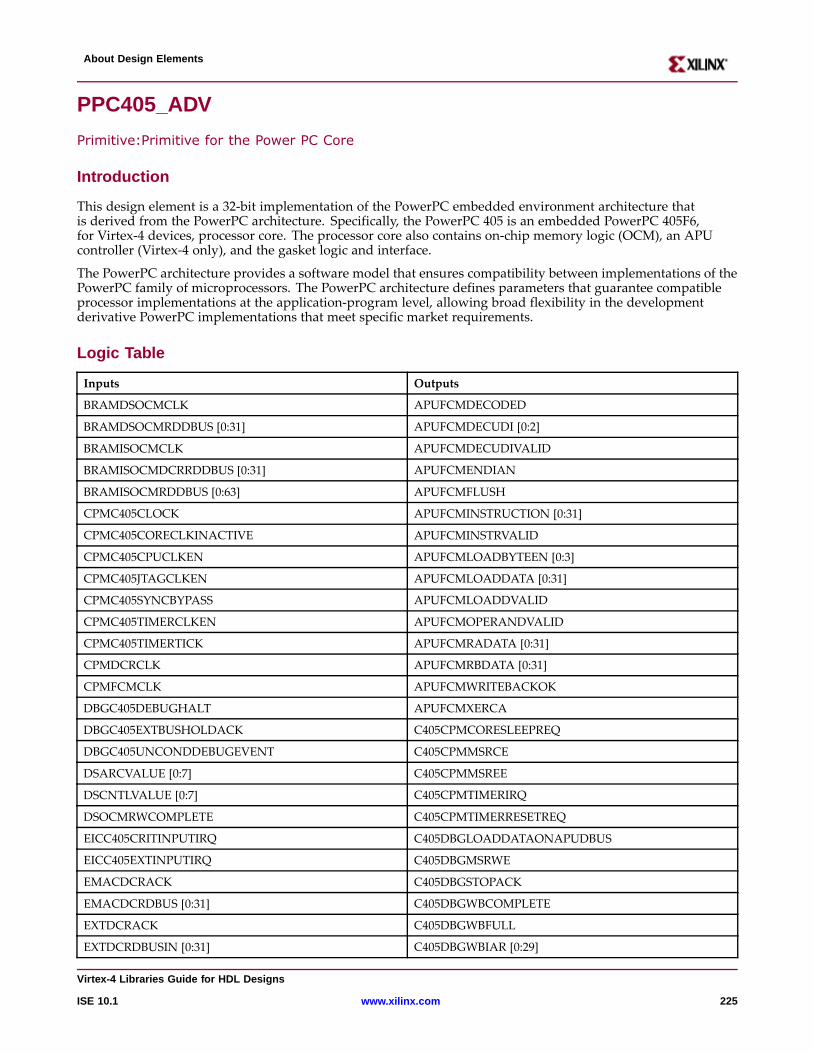
About Design Elements
PPC405_ADV
Primitive:Primitive for the Power PC Core
Intr oduction
This design element is a 32-bit implementation of the PowerPC embedded environment architecture thatis derived from the PowerPC architecture. Specifically, the PowerPC 405 is an embedded PowerPC 405F6,for Virtex-4 devices, processor core. The processor core also contains on-chip memory logic (OCM), an APUcontroller (Virtex-4 only), and the gasket logic and interface.
The PowerPC architecture provides a software model that ensures compatibility between implementations of thePowerPC family of microprocessors. The PowerPC architecture defines parameters that guarantee compatibleprocessor implementations at the application-program level, allowing broad flexibility in the developmentderivative PowerPC implementations that meet specific market requirements.
Logic Table
Inputs Outputs
BRAMDSOCMCLK APUFCMDECODED
BRAMDSOCMRDDBUS [0:31] APUFCMDECUDI [0:2]
BRAMISOCMCLK APUFCMDECUDIVALID
BRAMISOCMDCRRDDBUS [0:31] APUFCMENDIAN
BRAMISOCMRDDBUS [0:63] APUFCMFLUSH
CPMC405CLOCK APUFCMINSTRUCTION [0:31]
CPMC405CORECLKINACTIVE APUFCMINSTRVALID
CPMC405CPUCLKEN APUFCMLOADBYTEEN [0:3]
CPMC405JTAGCLKEN APUFCMLOADDATA [0:31]
CPMC405SYNCBYPASS APUFCMLOADDVALID
CPMC405TIMERCLKEN APUFCMOPERANDVALID
CPMC405TIMERTICK APUFCMRADATA [0:31]
CPMDCRCLK APUFCMRBDATA [0:31]
CPMFCMCLK APUFCMWRITEBACKOK
DBGC405DEBUGHALT APUFCMXERCA
DBGC405EXTBUSHOLDACK C405CPMCORESLEEPREQ
DBGC405UNCONDDEBUGEVENT C405CPMMSRCE
DSARCVALUE [0:7] C405CPMMSREE
DSCNTLVALUE [0:7] C405CPMTIMERIRQ
DSOCMRWCOMPLETE C405CPMTIMERRESETREQ
EICC405CRITINPUTIRQ C405DBGLOADDATAONAPUDBUS
EICC405EXTINPUTIRQ C405DBGMSRWE
EMACDCRACK C405DBGSTOPACK
EMACDCRDBUS [0:31] C405DBGWBCOMPLETE
EXTDCRACK C405DBGWBFULL
EXTDCRDBUSIN [0:31] C405DBGWBIAR [0:29]
Vir tex-4 Libraries Guide for HDL Designs
ISE 10.1 www.xilinx.com 225
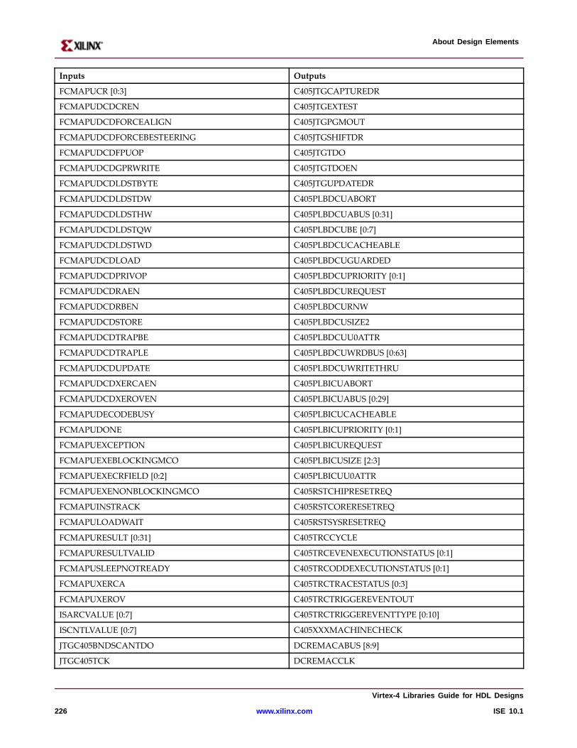
About Design Elements
Inputs Outputs
FCMAPUCR [0:3] C405JTGCAPTUREDR
FCMAPUDCDCREN C405JTGEXTEST
FCMAPUDCDFORCEALIGN C405JTGPGMOUT
FCMAPUDCDFORCEBESTEERING C405JTGSHIFTDR
FCMAPUDCDFPUOP C405JTGTDO
FCMAPUDCDGPRWRITE C405JTGTDOEN
FCMAPUDCDLDSTBYTE C405JTGUPDATEDR
FCMAPUDCDLDSTDW C405PLBDCUABORT
FCMAPUDCDLDSTHW C405PLBDCUABUS [0:31]
FCMAPUDCDLDSTQW C405PLBDCUBE [0:7]
FCMAPUDCDLDSTWD C405PLBDCUCACHEABLE
FCMAPUDCDLOAD C405PLBDCUGUARDED
FCMAPUDCDPRIVOP C405PLBDCUPRIORITY [0:1]
FCMAPUDCDRAEN C405PLBDCUREQUEST
FCMAPUDCDRBEN C405PLBDCURNW
FCMAPUDCDSTORE C405PLBDCUSIZE2
FCMAPUDCDTRAPBE C405PLBDCUU0ATTR
FCMAPUDCDTRAPLE C405PLBDCUWRDBUS [0:63]
FCMAPUDCDUPDATE C405PLBDCUWRITETHRU
FCMAPUDCDXERCAEN C405PLBICUABORT
FCMAPUDCDXEROVEN C405PLBICUABUS [0:29]
FCMAPUDECODEBUSY C405PLBICUCACHEABLE
FCMAPUDONE C405PLBICUPRIORITY [0:1]
FCMAPUEXCEPTION C405PLBICUREQUEST
FCMAPUEXEBLOCKINGMCO C405PLBICUSIZE [2:3]
FCMAPUEXECRFIELD [0:2] C405PLBICUU0ATTR
FCMAPUEXENONBLOCKINGMCO C405RSTCHIPRESETREQ
FCMAPUINSTRACK C405RSTCORERESETREQ
FCMAPULOADWAIT C405RSTSYSRESETREQ
FCMAPURESULT [0:31] C405TRCCYCLE
FCMAPURESULTVALID C405TRCEVENEXECUTIONSTATUS [0:1]
FCMAPUSLEEPNOTREADY C405TRCODDEXECUTIONSTATUS [0:1]
FCMAPUXERCA C405TRCTRACESTATUS [0:3]
FCMAPUXEROV C405TRCTRIGGEREVENTOUT
ISARCVALUE [0:7] C405TRCTRIGGEREVENTTYPE [0:10]
ISCNTLVALUE [0:7] C405XXXMACHINECHECK
JTGC405BNDSCANTDO DCREMACABUS [8:9]
JTGC405TCK DCREMACCLK
Vir tex-4 Libraries Guide for HDL Designs
226 www.xilinx.com ISE 10.1
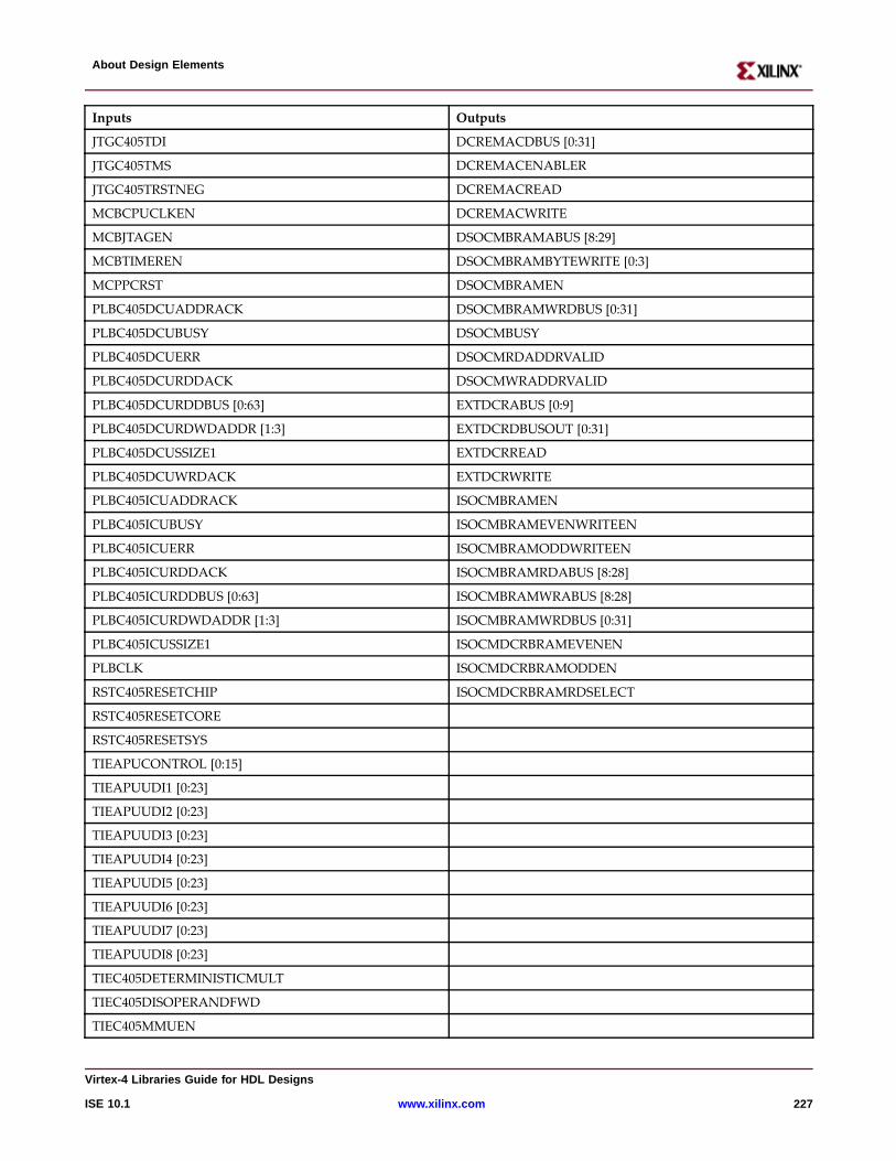
About Design Elements
Inputs Outputs
JTGC405TDI DCREMACDBUS [0:31]
JTGC405TMS DCREMACENABLER
JTGC405TRSTNEG DCREMACREAD
MCBCPUCLKEN DCREMACWRITE
MCBJTAGEN DSOCMBRAMABUS [8:29]
MCBTIMEREN DSOCMBRAMBYTEWRITE [0:3]
MCPPCRST DSOCMBRAMEN
PLBC405DCUADDRACK DSOCMBRAMWRDBUS [0:31]
PLBC405DCUBUSY DSOCMBUSY
PLBC405DCUERR DSOCMRDADDRVALID
PLBC405DCURDDACK DSOCMWRADDRVALID
PLBC405DCURDDBUS [0:63] EXTDCRABUS [0:9]
PLBC405DCURDWDADDR [1:3] EXTDCRDBUSOUT [0:31]
PLBC405DCUSSIZE1 EXTDCRREAD
PLBC405DCUWRDACK EXTDCRWRITE
PLBC405ICUADDRACK ISOCMBRAMEN
PLBC405ICUBUSY ISOCMBRAMEVENWRITEEN
PLBC405ICUERR ISOCMBRAMODDWRITEEN
PLBC405ICURDDACK ISOCMBRAMRDABUS [8:28]
PLBC405ICURDDBUS [0:63] ISOCMBRAMWRABUS [8:28]
PLBC405ICURDWDADDR [1:3] ISOCMBRAMWRDBUS [0:31]
PLBC405ICUSSIZE1 ISOCMDCRBRAMEVENEN
PLBCLK ISOCMDCRBRAMODDEN
RSTC405RESETCHIP ISOCMDCRBRAMRDSELECT
RSTC405RESETCORE
RSTC405RESETSYS
TIEAPUCONTROL [0:15]
TIEAPUUDI1 [0:23]
TIEAPUUDI2 [0:23]
TIEAPUUDI3 [0:23]
TIEAPUUDI4 [0:23]
TIEAPUUDI5 [0:23]
TIEAPUUDI6 [0:23]
TIEAPUUDI7 [0:23]
TIEAPUUDI8 [0:23]
TIEC405DETERMINISTICMULT
TIEC405DISOPERANDFWD
TIEC405MMUEN
Vir tex-4 Libraries Guide for HDL Designs
ISE 10.1 www.xilinx.com 227

About Design Elements
Inputs Outputs
TIEDCRADDR [0:5]
TIEPVRBIT10
TIEPVRBIT11
TIEPVRBIT28
TIEPVRBIT29
TIEPVRBIT30
TIEPVRBIT31
TIEPVRBIT8
TIEPVRBIT9
TRCC405TRACEDISABLE
TRCC405TRIGGEREVENTIN
Design Entr y Method
Instantiation Yes
Inference No
Coregen and wizards Recommended
Macro support No
For More Information
• See the Virtex-4 User Guide.
• See the Virtex-4 Data Sheets.
Vir tex-4 Libraries Guide for HDL Designs
228 www.xilinx.com ISE 10.1
About Design Elements
PULLDOWN
Primitive: Resistor to GND for Input Pads, Open-Drain, and 3-State Outputs
Intr oduction
This resistor element is connected to input, output, or bidirectional pads to guarantee a logic Low level fornodes that might float.
Por t Descriptions
Name Direction Width Function
O Output 1-Bit Pulldown output (connect directly to top level port)
Design Entr y Method
Instantiation Yes
Inference Recommended
Coregen and wizards No
Macro support No
VHDL Instantiation Template
Unless they already exist, copy the following two statements and paste them before the entity declaration.Library UNISIM;use UNISIM.vcomponents.all;
-- PULLDOWN:I/O Buffer Weak Pull-down-- All FPGA-- Xilinx HDL Libraries Guide, version 10.1.2
PULLDOWN_inst : PULLDOWNport map (O => O -- Pulldown output (connect directly to top-level port));
-- End of PULLDOWN_inst instantiation
Verilog Instantiation Template
// PULLDOWN:I/O Buffer Weak Pull-down// All FPGA// Xilinx HDL Libraries Guide, version 10.1.2
PULLDOWNPULLDOWN_inst (.O(O) // Pulldown output (connect directly to top-level port));
Vir tex-4 Libraries Guide for HDL Designs
ISE 10.1 www.xilinx.com 229
About Design Elements
// End of PULLDOWN_inst instantiation
For More Information
• See the Virtex-4 User Guide.
• See the Virtex-4 Data Sheets.
Vir tex-4 Libraries Guide for HDL Designs
230 www.xilinx.com ISE 10.1
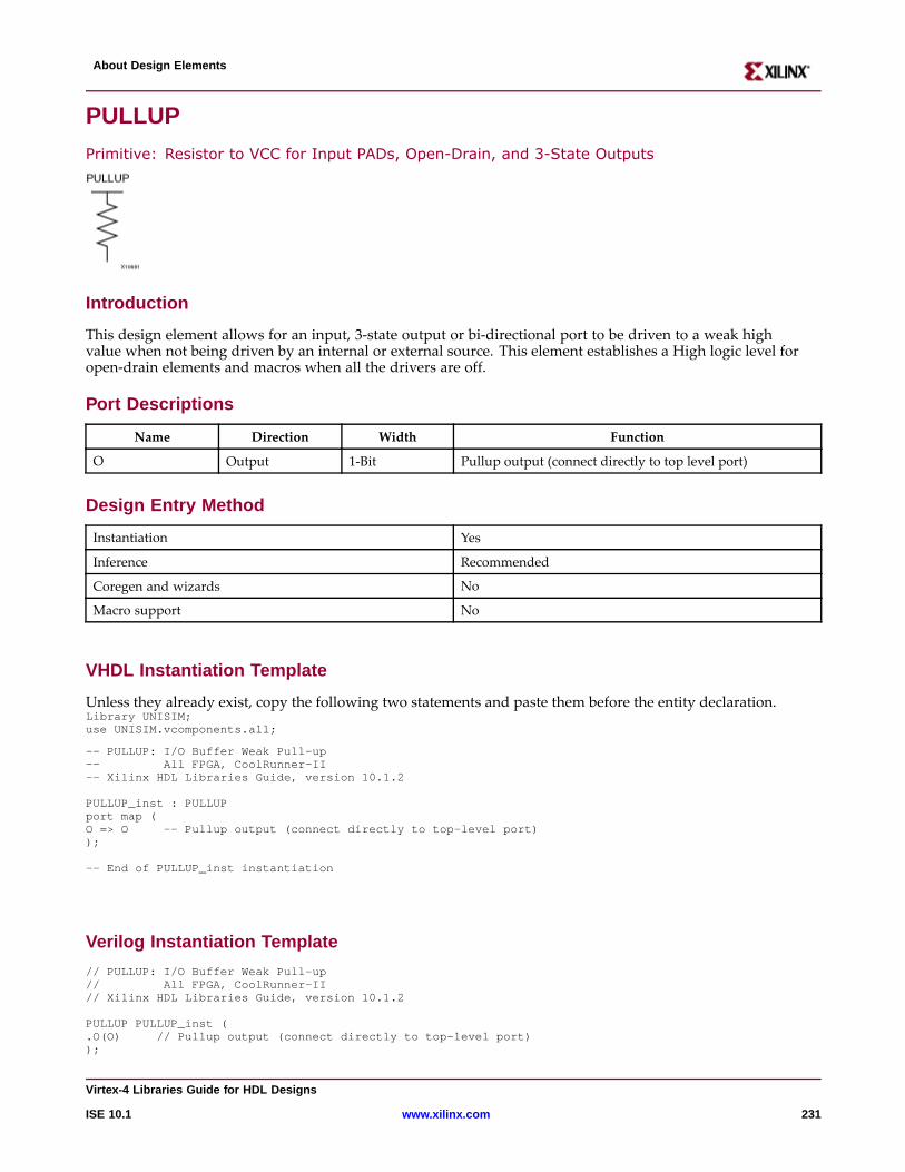
About Design Elements
PULLUP
Primitive: Resistor to VCC for Input PADs, Open-Drain, and 3-State Outputs
Intr oduction
This design element allows for an input, 3-state output or bi-directional port to be driven to a weak highvalue when not being driven by an internal or external source. This element establishes a High logic level foropen-drain elements and macros when all the drivers are off.
Por t Descriptions
Name Direction Width Function
O Output 1-Bit Pullup output (connect directly to top level port)
Design Entr y Method
Instantiation Yes
Inference Recommended
Coregen and wizards No
Macro support No
VHDL Instantiation Template
Unless they already exist, copy the following two statements and paste them before the entity declaration.Library UNISIM;use UNISIM.vcomponents.all;
-- PULLUP: I/O Buffer Weak Pull-up-- All FPGA, CoolRunner-II-- Xilinx HDL Libraries Guide, version 10.1.2
PULLUP_inst : PULLUPport map (O => O -- Pullup output (connect directly to top-level port));
-- End of PULLUP_inst instantiation
Verilog Instantiation Template
// PULLUP: I/O Buffer Weak Pull-up// All FPGA, CoolRunner-II// Xilinx HDL Libraries Guide, version 10.1.2
PULLUP PULLUP_inst (.O(O) // Pullup output (connect directly to top-level port));
Vir tex-4 Libraries Guide for HDL Designs
ISE 10.1 www.xilinx.com 231
About Design Elements
// End of PULLUP_inst instantiation
For More Information
• See the Virtex-4 User Guide.
• See the Virtex-4 Data Sheets.
Vir tex-4 Libraries Guide for HDL Designs
232 www.xilinx.com ISE 10.1
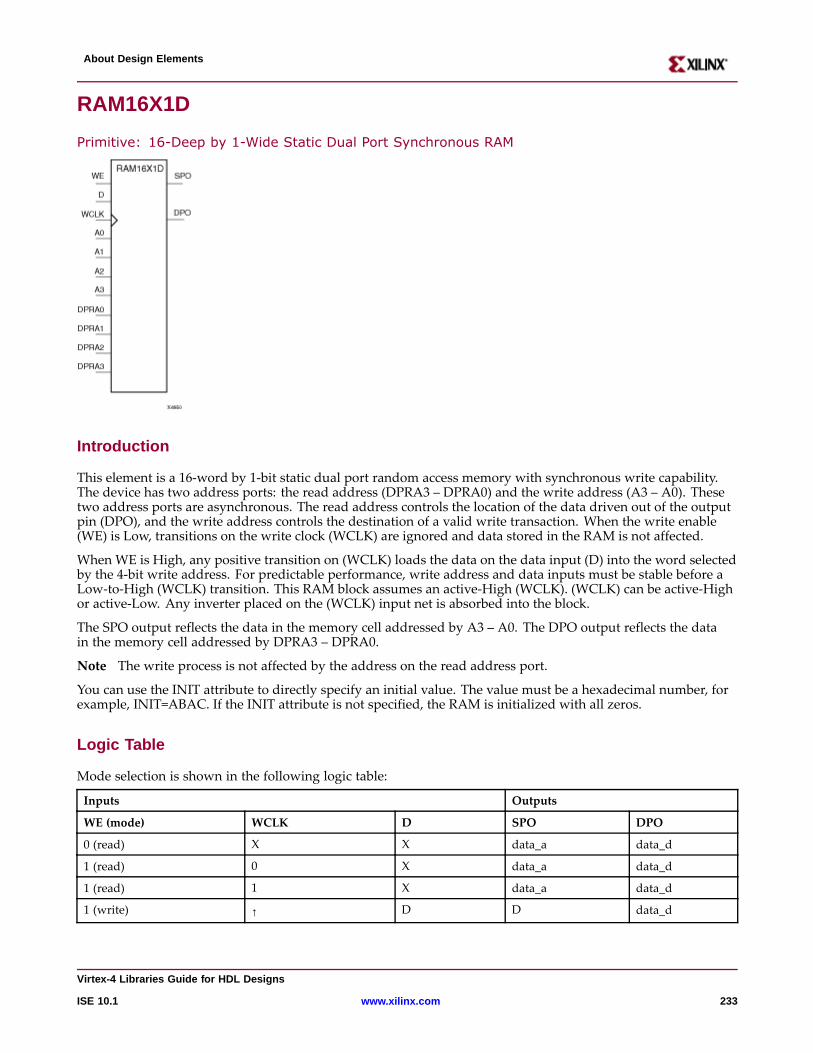
About Design Elements
RAM16X1D
Primitive: 16-Deep by 1-Wide Static Dual Port Synchronous RAM
Intr oduction
This element is a 16-word by 1-bit static dual port random access memory with synchronous write capability.The device has two address ports: the read address (DPRA3 – DPRA0) and the write address (A3 – A0). Thesetwo address ports are asynchronous. The read address controls the location of the data driven out of the outputpin (DPO), and the write address controls the destination of a valid write transaction. When the write enable(WE) is Low, transitions on the write clock (WCLK) are ignored and data stored in the RAM is not affected.
When WE is High, any positive transition on (WCLK) loads the data on the data input (D) into the word selectedby the 4-bit write address. For predictable performance, write address and data inputs must be stable before aLow-to-High (WCLK) transition. This RAM block assumes an active-High (WCLK). (WCLK) can be active-Highor active-Low. Any inverter placed on the (WCLK) input net is absorbed into the block.
The SPO output reflects the data in the memory cell addressed by A3 – A0. The DPO output reflects the datain the memory cell addressed by DPRA3 – DPRA0.
Note The write process is not affected by the address on the read address port.
You can use the INIT attribute to directly specify an initial value. The value must be a hexadecimal number, forexample, INIT=ABAC. If the INIT attribute is not specified, the RAM is initialized with all zeros.
Logic Table
Mode selection is shown in the following logic table:
Inputs Outputs
WE (mode) WCLK D SPO DPO
0 (read) X X data_a data_d
1 (read) 0 X data_a data_d
1 (read) 1 X data_a data_d
1 (write) ↑ D D data_d
Vir tex-4 Libraries Guide for HDL Designs
ISE 10.1 www.xilinx.com 233
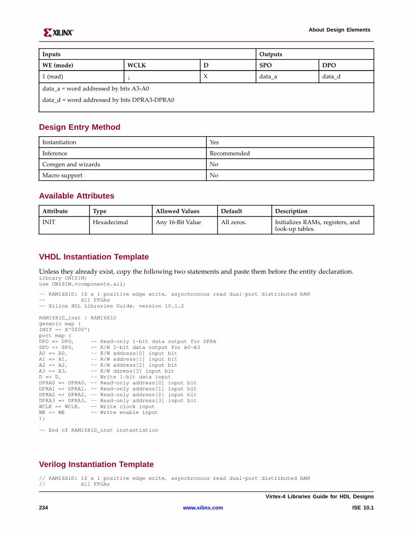
About Design Elements
Inputs Outputs
WE (mode) WCLK D SPO DPO
1 (read) ↓ X data_a data_d
data_a = word addressed by bits A3-A0
data_d = word addressed by bits DPRA3-DPRA0
Design Entr y Method
Instantiation Yes
Inference Recommended
Coregen and wizards No
Macro support No
Availab le Attrib utes
Attribute Type Allowed Values Default Description
INIT Hexadecimal Any 16-Bit Value All zeros. Initializes RAMs, registers, andlook-up tables.
VHDL Instantiation Template
Unless they already exist, copy the following two statements and paste them before the entity declaration.Library UNISIM;use UNISIM.vcomponents.all;
-- RAM16X1D: 16 x 1 positive edge write, asynchronous read dual-port distributed RAM-- All FPGAs-- Xilinx HDL Libraries Guide, version 10.1.2
RAM16X1D_inst : RAM16X1Dgeneric map (INIT => X"0000")port map (DPO => DPO, -- Read-only 1-bit data output for DPRASPO => SPO, -- R/W 1-bit data output for A0-A3A0 => A0, -- R/W address[0] input bitA1 => A1, -- R/W address[1] input bitA2 => A2, -- R/W address[2] input bitA3 => A3, -- R/W ddress[3] input bitD => D, -- Write 1-bit data inputDPRA0 => DPRA0, -- Read-only address[0] input bitDPRA1 => DPRA1, -- Read-only address[1] input bitDPRA2 => DPRA2, -- Read-only address[2] input bitDPRA3 => DPRA3, -- Read-only address[3] input bitWCLK=> WCLK, -- Write clock inputWE => WE -- Write enable input);
-- End of RAM16X1D_inst instantiation
Verilog Instantiation Template
// RAM16X1D: 16 x 1 positive edge write, asynchronous read dual-port distributed RAM// All FPGAs
Vir tex-4 Libraries Guide for HDL Designs
234 www.xilinx.com ISE 10.1
About Design Elements
// Xilinx HDL Libraries Guide, version 10.1.2
RAM16X1D#(.INIT(16’h0000) // Initial contents of RAM) RAM16X1D_inst (.DPO(DPO), // Read-only 1-bit data output for DPRA.SPO(SPO), // R/W 1-bit data output for A0-A3.A0(A0), // R/W address[0] input bit.A1(A1), // R/W address[1] input bit.A2(A2), // R/W address[2] input bit.A3(A3), // R/W address[3] input bit.D(D), // Write 1-bit data input.DPRA0(DPRA0), // Read address[0] input bit.DPRA1(DPRA1), // Read address[1] input bit.DPRA2(DPRA2), // Read address[2] input bit.DPRA3(DPRA3), // Read address[3] input bit.WCLK(WCLK), // Write clock input.WE(WE) // Write enable input);
// End of RAM16X1D_inst instantiation
For More Information
• See the Virtex-4 User Guide.
• See the Virtex-4 Data Sheets.
Vir tex-4 Libraries Guide for HDL Designs
ISE 10.1 www.xilinx.com 235
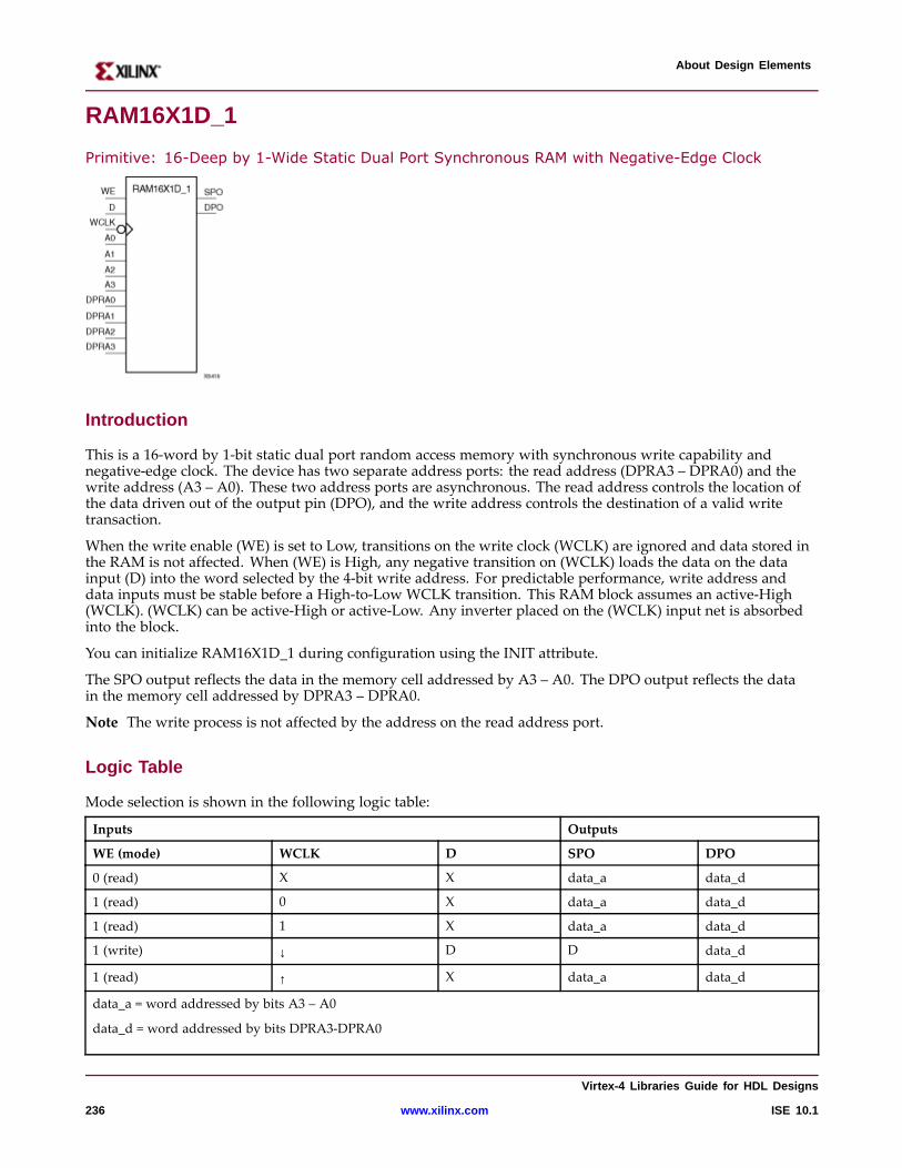
About Design Elements
RAM16X1D_1
Primitive: 16-Deep by 1-Wide Static Dual Port Synchronous RAM with Negative-Edge Clock
Intr oduction
This is a 16-word by 1-bit static dual port random access memory with synchronous write capability andnegative-edge clock. The device has two separate address ports: the read address (DPRA3 – DPRA0) and thewrite address (A3 – A0). These two address ports are asynchronous. The read address controls the location ofthe data driven out of the output pin (DPO), and the write address controls the destination of a valid writetransaction.
When the write enable (WE) is set to Low, transitions on the write clock (WCLK) are ignored and data stored inthe RAM is not affected. When (WE) is High, any negative transition on (WCLK) loads the data on the datainput (D) into the word selected by the 4-bit write address. For predictable performance, write address anddata inputs must be stable before a High-to-Low WCLK transition. This RAM block assumes an active-High(WCLK). (WCLK) can be active-High or active-Low. Any inverter placed on the (WCLK) input net is absorbedinto the block.
You can initialize RAM16X1D_1 during configuration using the INIT attribute.
The SPO output reflects the data in the memory cell addressed by A3 – A0. The DPO output reflects the datain the memory cell addressed by DPRA3 – DPRA0.
Note The write process is not affected by the address on the read address port.
Logic Table
Mode selection is shown in the following logic table:
Inputs Outputs
WE (mode) WCLK D SPO DPO
0 (read) X X data_a data_d
1 (read) 0 X data_a data_d
1 (read) 1 X data_a data_d
1 (write) ↓ D D data_d
1 (read) ↑ X data_a data_d
data_a = word addressed by bits A3 – A0
data_d = word addressed by bits DPRA3-DPRA0
Vir tex-4 Libraries Guide for HDL Designs
236 www.xilinx.com ISE 10.1
About Design Elements
Por t Descriptions
Name Direction Width Function
DPO Output 1-Bit Read-only 1-Bit data output
SPO Output 1-Bit R/W 1-Bit data output
A0 Input 1-Bit R/W address[0] input
A1 Input 1-Bit R/W address[1] input
A2 Input 1-Bit R/W address[2] input
A3 Input 1-Bit R/W address[3] input
D Input 1-Bit Write 1-Bit data input
DPRA0 Input 1-Bit Read-only address[0] input
DPRA1 Input 1-Bit Read-only address[1] input
DPRA2 Input 1-Bit Read-only address[2] input
DPRA3 Input 1-Bit Read-only address[3] input
WCLK Input 1-Bit Write clock input
WE Input 1-Bit Write enable input
Design Entr y Method
Instantiation Yes
Inference Recommended
Coregen and wizards No
Macro support No
Availab le Attrib utes
Attribute Type Allowed Values Default Description
INIT Hexadecimal Any 16-Bit Value All zeros Initializes RAMs, registers, andlook-up tables.
VHDL Instantiation Template
Unless they already exist, copy the following two statements and paste them before the entity declaration.Library UNISIM;use UNISIM.vcomponents.all;
-- RAM16X1D_1: 16 x 1 negative edge write, asynchronous read dual-port distributed RAM-- All FPGA-- Xilinx HDL Libraries Guide, version 10.1.2
RAM16X1D_1_inst : RAM16X1D_1generic map (INIT => X"0000")port map (DPO => DPO, -- Read-only 1-bit data output for DPRASPO => SPO, -- R/W 1-bit data output for A0-A3A0 => A0, -- R/W address[0] input bitA1 => A1, -- R/W address[1] input bitA2 => A2, -- R/W address[2] input bitA3 => A3, -- R/W ddress[3] input bitD => D, -- Write 1-bit data inputDPRA0 => DPRA0, -- Read-only address[0] input bit
Vir tex-4 Libraries Guide for HDL Designs
ISE 10.1 www.xilinx.com 237
About Design Elements
DPRA1 => DPRA1, -- Read-only address[1] input bitDPRA2 => DPRA2, -- Read-only address[2] input bitDPRA3 => DPRA3, -- Read-only address[3] input bitWCLK=> WCLK, -- Write clock inputWE => WE -- Write enable input);
-- End of RAM16X1D_1_inst instantiation
Verilog Instantiation Template
// RAM16X1D_1: 16 x 1 negative edge write, asynchronous read dual-port distributed RAM// Virtex/E/-II/-II-Pro, Spartan-II/IIE/3/3E/3A// Xilinx HDL Libraries Guide, version 10.1.2
RAM16X1D_1 #(.INIT(16’h0000) // Initial contents of RAM) RAM16X1D_1_inst (.DPO(DPO), // Read-only 1-bit data output.SPO(SPO), // R/W 1-bit data output.A0(A0), // R/W address[0] input bit.A1(A1), // R/W address[1] input bit.A2(A2), // R/W address[2] input bit.A3(A3), // R/W address[3] input bit.D(D), // Write 1-bit data input.DPRA0(DPRA0), // Read-only address[0] input bit.DPRA1(DPRA1), // Read-only address[1] input bit.DPRA2(DPRA2), // Read-only address[2] input bit.DPRA3(DPRA3), // Read-only address[3] input bit.WCLK(WCLK), // Write clock input.WE(WE) // Write enable input);
// End of RAM16X1D_1_inst instantiation
For More Information
• See the Virtex-4 User Guide.
• See the Virtex-4 Data Sheets.
Vir tex-4 Libraries Guide for HDL Designs
238 www.xilinx.com ISE 10.1
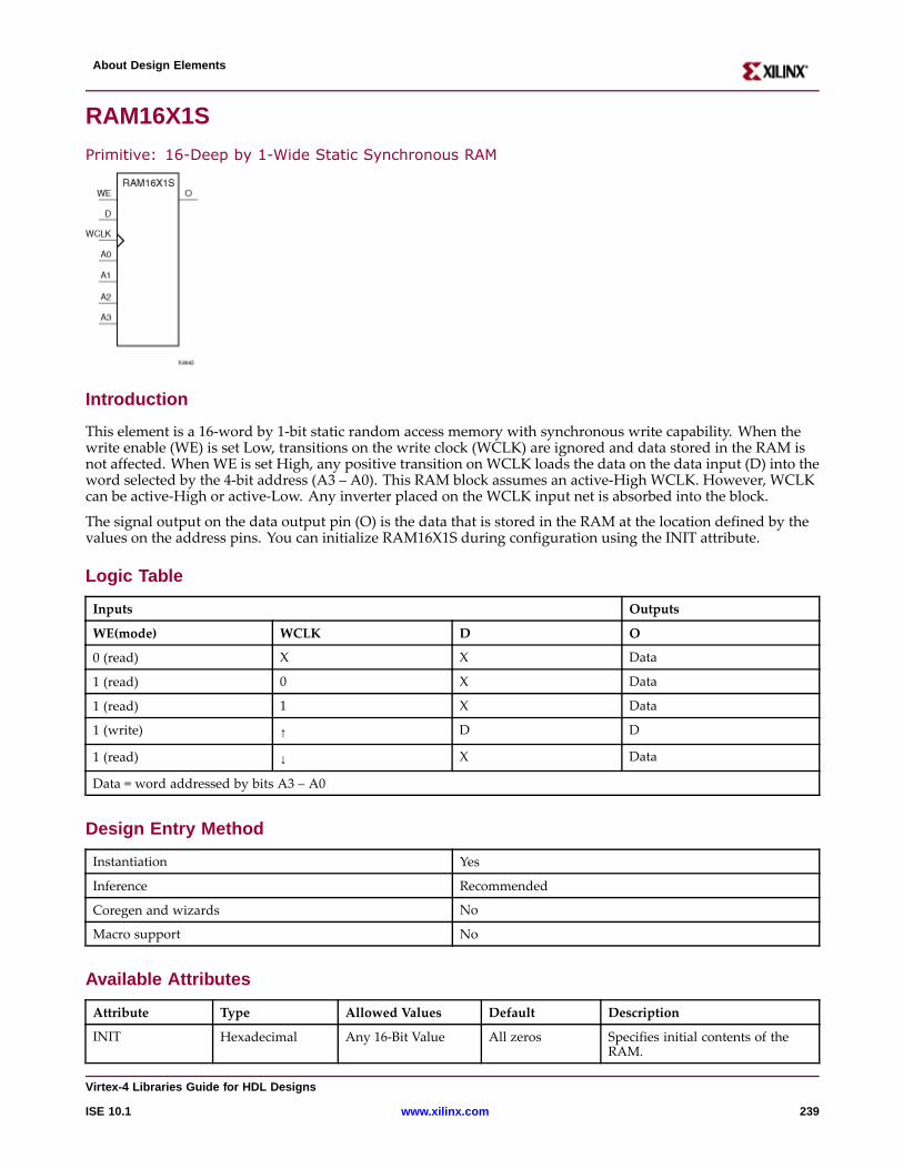
About Design Elements
RAM16X1S
Primitive: 16-Deep by 1-Wide Static Synchronous RAM
Intr oduction
This element is a 16-word by 1-bit static random access memory with synchronous write capability. When thewrite enable (WE) is set Low, transitions on the write clock (WCLK) are ignored and data stored in the RAM isnot affected. When WE is set High, any positive transition on WCLK loads the data on the data input (D) into theword selected by the 4-bit address (A3 – A0). This RAM block assumes an active-High WCLK. However, WCLKcan be active-High or active-Low. Any inverter placed on the WCLK input net is absorbed into the block.
The signal output on the data output pin (O) is the data that is stored in the RAM at the location defined by thevalues on the address pins. You can initialize RAM16X1S during configuration using the INIT attribute.
Logic Table
Inputs Outputs
WE(mode) WCLK D O
0 (read) X X Data
1 (read) 0 X Data
1 (read) 1 X Data
1 (write) ↑ D D
1 (read) ↓ X Data
Data = word addressed by bits A3 – A0
Design Entr y Method
Instantiation Yes
Inference Recommended
Coregen and wizards No
Macro support No
Availab le Attrib utes
Attribute Type Allowed Values Default Description
INIT Hexadecimal Any 16-Bit Value All zeros Specifies initial contents of theRAM.
Vir tex-4 Libraries Guide for HDL Designs
ISE 10.1 www.xilinx.com 239
About Design Elements
VHDL Instantiation Template
Unless they already exist, copy the following two statements and paste them before the entity declaration.Library UNISIM;use UNISIM.vcomponents.all;
-- RAM16X1S: 16 x 1 posedge write distributed => LUT RAM-- All FPGA-- Xilinx HDL Libraries Guide, version 10.1.2
RAM16X1S_inst : RAM16X1Sgeneric map (INIT => X"0000")port map (O => O, -- RAMoutputA0 => A0, -- RAMaddress[0] inputA1 => A1, -- RAMaddress[1] inputA2 => A2, -- RAMaddress[2] inputA3 => A3, -- RAMaddress[3] inputD => D, -- RAMdata inputWCLK=> WCLK, -- Write clock inputWE => WE -- Write enable input);
-- End of RAM16X1S_inst instantiation
Verilog Instantiation Template
// RAM16X1S: 16 x 1 posedge write distributed (LUT) RAM// All FPGA// Xilinx HDL Libraries Guide, version 10.1.2
RAM16X1S#(.INIT(16’h0000) // Initial contents of RAM) RAM16X1S_inst (.O(O), // RAMoutput.A0(A0), // RAMaddress[0] input.A1(A1), // RAMaddress[1] input.A2(A2), // RAMaddress[2] input.A3(A3), // RAMaddress[3] input.D(D), // RAMdata input.WCLK(WCLK), // Write clock input.WE(WE) // Write enable input);
// End of RAM16X1S_inst instantiation
For More Information
• See the Virtex-4 User Guide.
• See the Virtex-4 Data Sheets.
Vir tex-4 Libraries Guide for HDL Designs
240 www.xilinx.com ISE 10.1
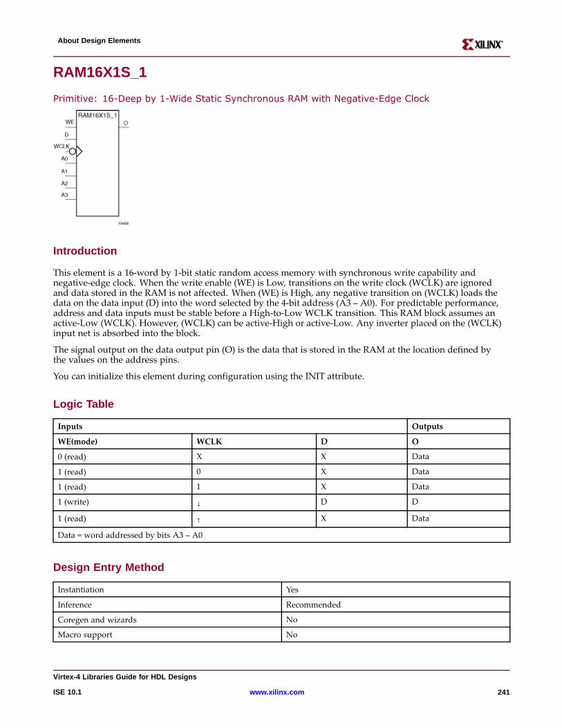
About Design Elements
RAM16X1S_1
Primitive: 16-Deep by 1-Wide Static Synchronous RAM with Negative-Edge Clock
Intr oduction
This element is a 16-word by 1-bit static random access memory with synchronous write capability andnegative-edge clock. When the write enable (WE) is Low, transitions on the write clock (WCLK) are ignoredand data stored in the RAM is not affected. When (WE) is High, any negative transition on (WCLK) loads thedata on the data input (D) into the word selected by the 4-bit address (A3 – A0). For predictable performance,address and data inputs must be stable before a High-to-Low WCLK transition. This RAM block assumes anactive-Low (WCLK). However, (WCLK) can be active-High or active-Low. Any inverter placed on the (WCLK)input net is absorbed into the block.
The signal output on the data output pin (O) is the data that is stored in the RAM at the location defined bythe values on the address pins.
You can initialize this element during configuration using the INIT attribute.
Logic Table
Inputs Outputs
WE(mode) WCLK D O
0 (read) X X Data
1 (read) 0 X Data
1 (read) 1 X Data
1 (write) ↓ D D
1 (read) ↑ X Data
Data = word addressed by bits A3 – A0
Design Entr y Method
Instantiation Yes
Inference Recommended
Coregen and wizards No
Macro support No
Vir tex-4 Libraries Guide for HDL Designs
ISE 10.1 www.xilinx.com 241
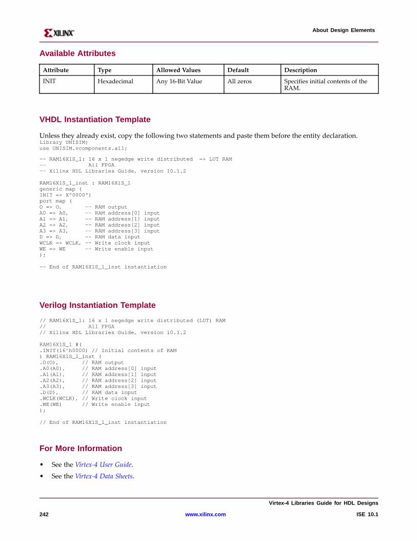
About Design Elements
Availab le Attrib utes
Attribute Type Allowed Values Default Description
INIT Hexadecimal Any 16-Bit Value All zeros Specifies initial contents of theRAM.
VHDL Instantiation Template
Unless they already exist, copy the following two statements and paste them before the entity declaration.Library UNISIM;use UNISIM.vcomponents.all;
-- RAM16X1S_1: 16 x 1 negedge write distributed => LUT RAM-- All FPGA-- Xilinx HDL Libraries Guide, version 10.1.2
RAM16X1S_1_inst : RAM16X1S_1generic map (INIT => X"0000")port map (O => O, -- RAMoutputA0 => A0, -- RAMaddress[0] inputA1 => A1, -- RAMaddress[1] inputA2 => A2, -- RAMaddress[2] inputA3 => A3, -- RAMaddress[3] inputD => D, -- RAMdata inputWCLK=> WCLK, -- Write clock inputWE => WE -- Write enable input);
-- End of RAM16X1S_1_inst instantiation
Verilog Instantiation Template
// RAM16X1S_1: 16 x 1 negedge write distributed (LUT) RAM// All FPGA// Xilinx HDL Libraries Guide, version 10.1.2
RAM16X1S_1 #(.INIT(16’h0000) // Initial contents of RAM) RAM16X1S_1_inst (.O(O), // RAMoutput.A0(A0), // RAMaddress[0] input.A1(A1), // RAMaddress[1] input.A2(A2), // RAMaddress[2] input.A3(A3), // RAMaddress[3] input.D(D), // RAMdata input.WCLK(WCLK), // Write clock input.WE(WE) // Write enable input);
// End of RAM16X1S_1_inst instantiation
For More Information
• See the Virtex-4 User Guide.
• See the Virtex-4 Data Sheets.
Vir tex-4 Libraries Guide for HDL Designs
242 www.xilinx.com ISE 10.1
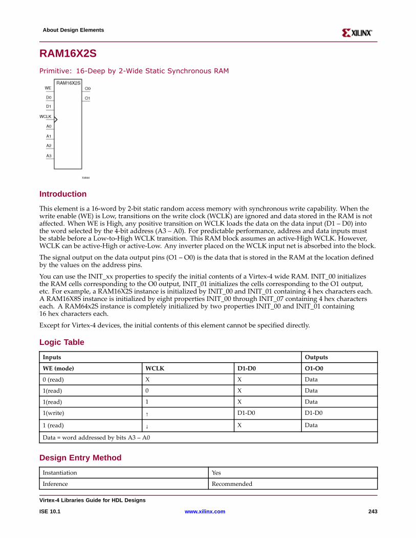
About Design Elements
RAM16X2S
Primitive: 16-Deep by 2-Wide Static Synchronous RAM
Intr oduction
This element is a 16-word by 2-bit static random access memory with synchronous write capability. When thewrite enable (WE) is Low, transitions on the write clock (WCLK) are ignored and data stored in the RAM is notaffected. When WE is High, any positive transition on WCLK loads the data on the data input (D1 – D0) intothe word selected by the 4-bit address (A3 – A0). For predictable performance, address and data inputs mustbe stable before a Low-to-High WCLK transition. This RAM block assumes an active-High WCLK. However,WCLK can be active-High or active-Low. Any inverter placed on the WCLK input net is absorbed into the block.
The signal output on the data output pins (O1 – O0) is the data that is stored in the RAM at the location definedby the values on the address pins.
You can use the INIT_xx properties to specify the initial contents of a Virtex-4 wide RAM. INIT_00 initializesthe RAM cells corresponding to the O0 output, INIT_01 initializes the cells corresponding to the O1 output,etc. For example, a RAM16X2S instance is initialized by INIT_00 and INIT_01 containing 4 hex characters each.A RAM16X8S instance is initialized by eight properties INIT_00 through INIT_07 containing 4 hex characterseach. A RAM64x2S instance is completely initialized by two properties INIT_00 and INIT_01 containing16 hex characters each.
Except for Virtex-4 devices, the initial contents of this element cannot be specified directly.
Logic Table
Inputs Outputs
WE (mode) WCLK D1-D0 O1-O0
0 (read) X X Data
1(read) 0 X Data
1(read) 1 X Data
1(write) ↑ D1-D0 D1-D0
1 (read) ↓ X Data
Data = word addressed by bits A3 – A0
Design Entr y Method
Instantiation Yes
Inference Recommended
Vir tex-4 Libraries Guide for HDL Designs
ISE 10.1 www.xilinx.com 243
About Design Elements
Coregen and wizards No
Macro support No
Availab le Attrib utes
Attribute Type Allowed Values Default Description
INIT_00 to INIT_01 Hexadecimal Any 16-Bit Value All zeros Initializes RAMs, registers, andlook-up tables.
VHDL Instantiation Template
Unless they already exist, copy the following two statements and paste them before the entity declaration.Library UNISIM;use UNISIM.vcomponents.all;
-- RAM16X2S: 16 x 2 posedge write distributed => LUT RAM-- Virtex-II/II-Pro, Spartan-3/3E/3A-- Xilinx HDL Libraries Guide, version 10.1.2
RAM16X2S_inst : RAM16X2Sgeneric map (INIT_00 => X"0000", -- INIT for bit 0 of RAMINIT_01 => X"0000") -- INIT for bit 1 of RAMport map (O0 => O0, -- RAMdata[0] outputO1 => O1, -- RAMdata[1] outputA0 => A0, -- RAMaddress[0] inputA1 => A1, -- RAMaddress[1] inputA2 => A2, -- RAMaddress[2] inputA3 => A3, -- RAMaddress[3] inputD0 => D0, -- RAMdata[0] inputD1 => D1, -- RAMdata[1] inputWCLK=> WCLK, -- Write clock inputWE => WE -- Write enable input);
-- End of RAM16X2S_inst instantiation
Verilog Instantiation Template
// RAM16X2S: 16 x 2 posedge write distributed (LUT) RAM// Virtex-II/II-Pro, Spartan-3/3E/3A// Xilinx HDL Libraries Guide, version 10.1.2
RAM16X2S#(.INIT_00(16’h0000), // Initial contents of bit 0 of RAM.INIT_01(16’h0000) // Initial contents of bit 1 of RAM) RAM16X2S_inst (.O0(O0), // RAMdata[0] output.O1(O1), // RAMdata[1] output.A0(A0), // RAMaddress[0] input.A1(A1), // RAMaddress[1] input.A2(A2), // RAMaddress[2] input.A3(A3), // RAMaddress[3] input.D0(D0), // RAMdata[0] input.D1(D1), // RAMdata[1] input.WCLK(WCLK), // Write clock input.WE(WE) // Write enable input);
// End of RAM16X2S_inst instantiation
Vir tex-4 Libraries Guide for HDL Designs
244 www.xilinx.com ISE 10.1

About Design Elements
For More Information
• See the Virtex-4 User Guide.
• See the Virtex-4 Data Sheets.
Vir tex-4 Libraries Guide for HDL Designs
ISE 10.1 www.xilinx.com 245
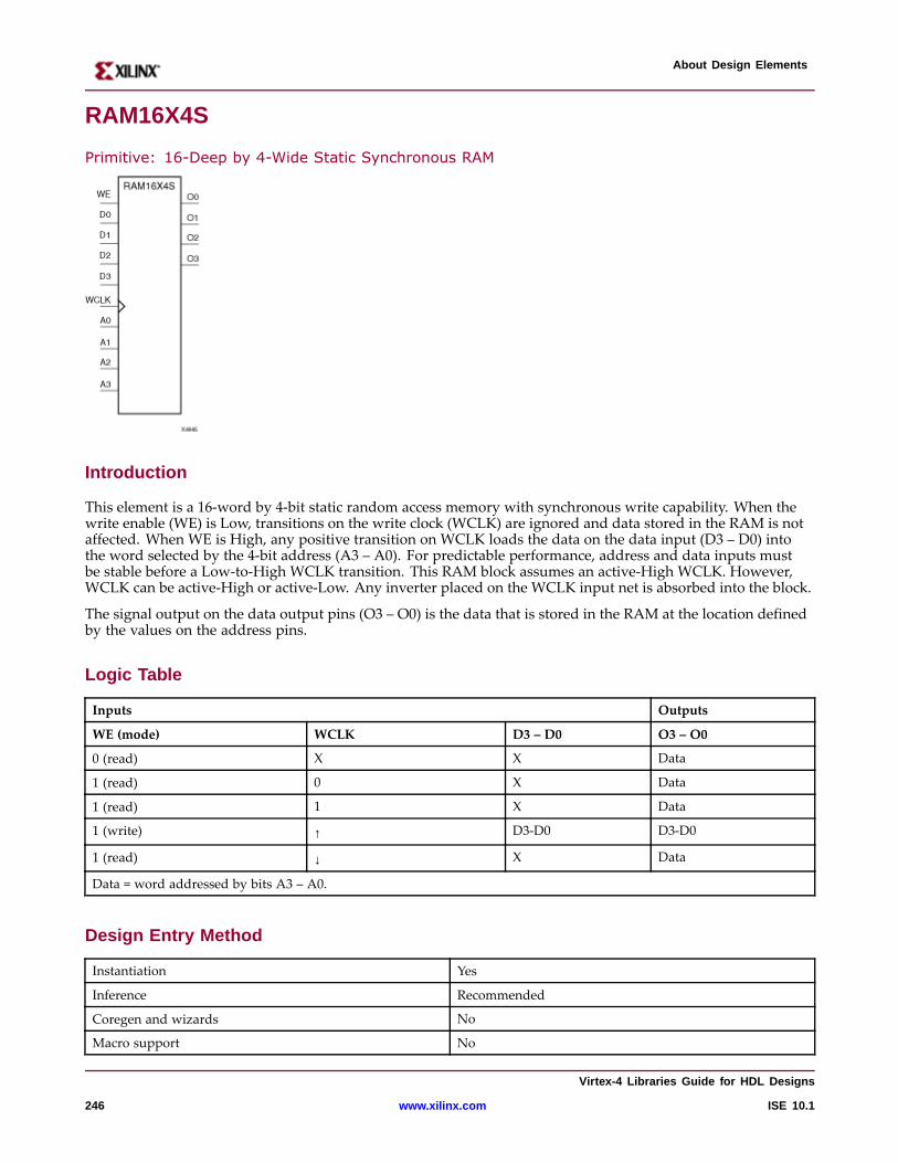
About Design Elements
RAM16X4S
Primitive: 16-Deep by 4-Wide Static Synchronous RAM
Intr oduction
This element is a 16-word by 4-bit static random access memory with synchronous write capability. When thewrite enable (WE) is Low, transitions on the write clock (WCLK) are ignored and data stored in the RAM is notaffected. When WE is High, any positive transition on WCLK loads the data on the data input (D3 – D0) intothe word selected by the 4-bit address (A3 – A0). For predictable performance, address and data inputs mustbe stable before a Low-to-High WCLK transition. This RAM block assumes an active-High WCLK. However,WCLK can be active-High or active-Low. Any inverter placed on the WCLK input net is absorbed into the block.
The signal output on the data output pins (O3 – O0) is the data that is stored in the RAM at the location definedby the values on the address pins.
Logic Table
Inputs Outputs
WE (mode) WCLK D3 – D0 O3 – O0
0 (read) X X Data
1 (read) 0 X Data
1 (read) 1 X Data
1 (write) ↑ D3-D0 D3-D0
1 (read) ↓ X Data
Data = word addressed by bits A3 – A0.
Design Entr y Method
Instantiation Yes
Inference Recommended
Coregen and wizards No
Macro support No
Vir tex-4 Libraries Guide for HDL Designs
246 www.xilinx.com ISE 10.1
About Design Elements
Availab le Attrib utes
Attribute Type Allowed Values Default Description
INIT_00 to INIT_03 Hexadecimal Any 16-Bit Value All zeros INIT for bit 0 of RAM
VHDL Instantiation Template
Unless they already exist, copy the following two statements and paste them before the entity declaration.Library UNISIM;use UNISIM.vcomponents.all;
-- RAM16X4S: 16 x 4 posedge write distributed => LUT RAM-- Virtex-II/II-Pro, Spartan-3/3E/3A-- Xilinx HDL Libraries Guide, version 10.1.2
RAM16X4S_inst : RAM16X4Sgeneric map (INIT_00 => X"0000", -- INIT for bit 0 of RAMINIT_01 => X"0000", -- INIT for bit 1 of RAMINIT_02 => X"0000", -- INIT for bit 2 of RAMINIT_03 => X"0000") -- INIT for bit 3 of RAMport map (O0 => O0, -- RAMdata[0] outputO1 => O1, -- RAMdata[1] outputO2 => O2, -- RAMdata[2] outputO3 => O3, -- RAMdata[3] outputA0 => A0, -- RAMaddress[0] inputA1 => A1, -- RAMaddress[1] inputA2 => A2, -- RAMaddress[2] inputA3 => A3, -- RAMaddress[3] inputD0 => D0, -- RAMdata[0] inputD1 => D1, -- RAMdata[1] inputD2 => D2, -- RAMdata[2] inputD3 => D3, -- RAMdata[3] inputWCLK=> WCLK, -- Write clock inputWE => WE -- Write enable input);
-- End of RAM16X4S_inst instantiation
Verilog Instantiation Template
// RAM16X4S: 16 x 4 posedge write distributed (LUT) RAM// Virtex-II/II-Pro, Spartan-3/3E/3A// Xilinx HDL Libraries Guide, version 10.1.2
RAM16X4S#(.INIT_00(16’h0000), // INIT for bit 0 of RAM.INIT_01(16’h0000), // INIT for bit 1 of RAM.INIT_02(16’h0000), // INIT for bit 2 of RAM.INIT_03(16’h0000) // INIT for bit 3 of RAM) RAM16X4S_inst (.O0(O0), // RAMdata[0] output.O1(O1), // RAMdata[1] output.O2(O2), // RAMdata[2] output.O3(O3), // RAMdata[3] output.A0(A0), // RAMaddress[0] input.A1(A1), // RAMaddress[1] input.A2(A2), // RAMaddress[2] input.A3(A3), // RAMaddress[3] input.D0(D0), // RAMdata[0] input.D1(D1), // RAMdata[1] input.D2(D2), // RAMdata[2] input.D3(D3), // RAMdata[3] input.WCLK(WCLK), // Write clock input
Vir tex-4 Libraries Guide for HDL Designs
ISE 10.1 www.xilinx.com 247
About Design Elements
.WE(WE) // Write enable input);
// End of RAM16X4S_inst instantiation
For More Information
• See the Virtex-4 User Guide.
• See the Virtex-4 Data Sheets.
Vir tex-4 Libraries Guide for HDL Designs
248 www.xilinx.com ISE 10.1
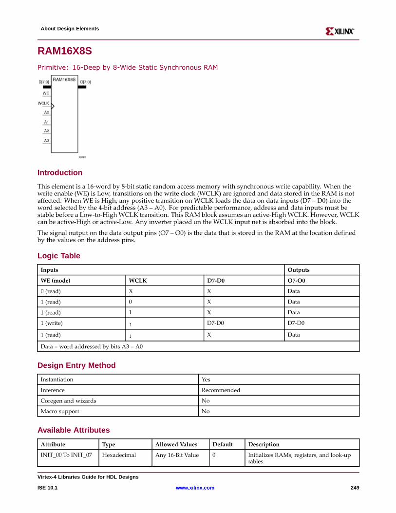
About Design Elements
RAM16X8S
Primitive: 16-Deep by 8-Wide Static Synchronous RAM
Intr oduction
This element is a 16-word by 8-bit static random access memory with synchronous write capability. When thewrite enable (WE) is Low, transitions on the write clock (WCLK) are ignored and data stored in the RAM is notaffected. When WE is High, any positive transition on WCLK loads the data on data inputs (D7 – D0) into theword selected by the 4-bit address (A3 – A0). For predictable performance, address and data inputs must bestable before a Low-to-HighWCLK transition. This RAM block assumes an active-HighWCLK. However, WCLKcan be active-High or active-Low. Any inverter placed on the WCLK input net is absorbed into the block.
The signal output on the data output pins (O7 – O0) is the data that is stored in the RAM at the location definedby the values on the address pins.
Logic Table
Inputs Outputs
WE (mode) WCLK D7-D0 O7-O0
0 (read) X X Data
1 (read) 0 X Data
1 (read) 1 X Data
1 (write) ↑ D7-D0 D7-D0
1 (read) ↓ X Data
Data = word addressed by bits A3 – A0
Design Entr y Method
Instantiation Yes
Inference Recommended
Coregen and wizards No
Macro support No
Availab le Attrib utes
Attribute Type Allowed Values Default Description
INIT_00 To INIT_07 Hexadecimal Any 16-Bit Value 0 Initializes RAMs, registers, and look-uptables.
Vir tex-4 Libraries Guide for HDL Designs
ISE 10.1 www.xilinx.com 249
About Design Elements
VHDL Instantiation Template
Unless they already exist, copy the following two statements and paste them before the entity declaration.Library UNISIM;use UNISIM.vcomponents.all;
-- RAM16X8S: 16 x 8 posedge write distributed => LUT RAM-- Virtex-II/II-Pro-- Xilinx HDL Libraries Guide, version 10.1.2
RAM16X8S_inst : RAM16X8Sgeneric map (INIT_00 => X"0000", -- INIT for bit 0 of RAMINIT_01 => X"0000", -- INIT for bit 1 of RAMINIT_02 => X"0000", -- INIT for bit 2 of RAMINIT_03 => X"0000", -- INIT for bit 3 of RAMINIT_04 => X"0000", -- INIT for bit 4 of RAMINIT_05 => X"0000", -- INIT for bit 5 of RAMINIT_06 => X"0000", -- INIT for bit 6 of RAMINIT_07 => X"0000") -- INIT for bit 7 of RAMport map (O => O, -- 8-bit RAMdata outputA0 => A0, -- RAMaddress[0] inputA1 => A1, -- RAMaddress[1] inputA2 => A2, -- RAMaddress[2] inputA3 => A3, -- RAMaddress[3] inputD => D, -- 8-bit RAMdata inputWCLK=> WCLK, -- Write clock inputWE => WE -- Write enable input);
-- End of RAM16X8S_inst instantiation
Verilog Instantiation Template
// RAM16X8S: 16 x 8 posedge write distributed (LUT) RAM// Virtex-II/II-Pro// Xilinx HDL Libraries Guide, version 10.1.2
RAM16X8S#(.INIT_00(16’h0000), // INIT for bit 0 of RAM.INIT_01(16’h0000), // INIT for bit 1 of RAM.INIT_02(16’h0000), // INIT for bit 2 of RAM.INIT_03(16’h0000), // INIT for bit 3 of RAM.INIT_04(16’h0000), // INIT for bit 4 of RAM.INIT_05(16’h0000), // INIT for bit 5 of RAM.INIT_06(16’h0000), // INIT for bit 6 of RAM.INIT_07(16’h0000) // INIT for bit 7 of RAM) RAM16X8S_inst (.O(O), // 8-bit RAMdata output.A0(A0), // RAMaddress[0] input.A1(A1), // RAMaddress[1] input.A2(A2), // RAMaddress[2] input.A3(A3), // RAMaddress[3] input.D(D), // 8-bit RAMdata input.WCLK(WCLK), // Write clock input.WE(WE) // Write enable input);
// End of RAM16X8S_inst instantiation
Vir tex-4 Libraries Guide for HDL Designs
250 www.xilinx.com ISE 10.1

About Design Elements
For More Information
• See the Virtex-4 User Guide.
• See the Virtex-4 Data Sheets.
Vir tex-4 Libraries Guide for HDL Designs
ISE 10.1 www.xilinx.com 251
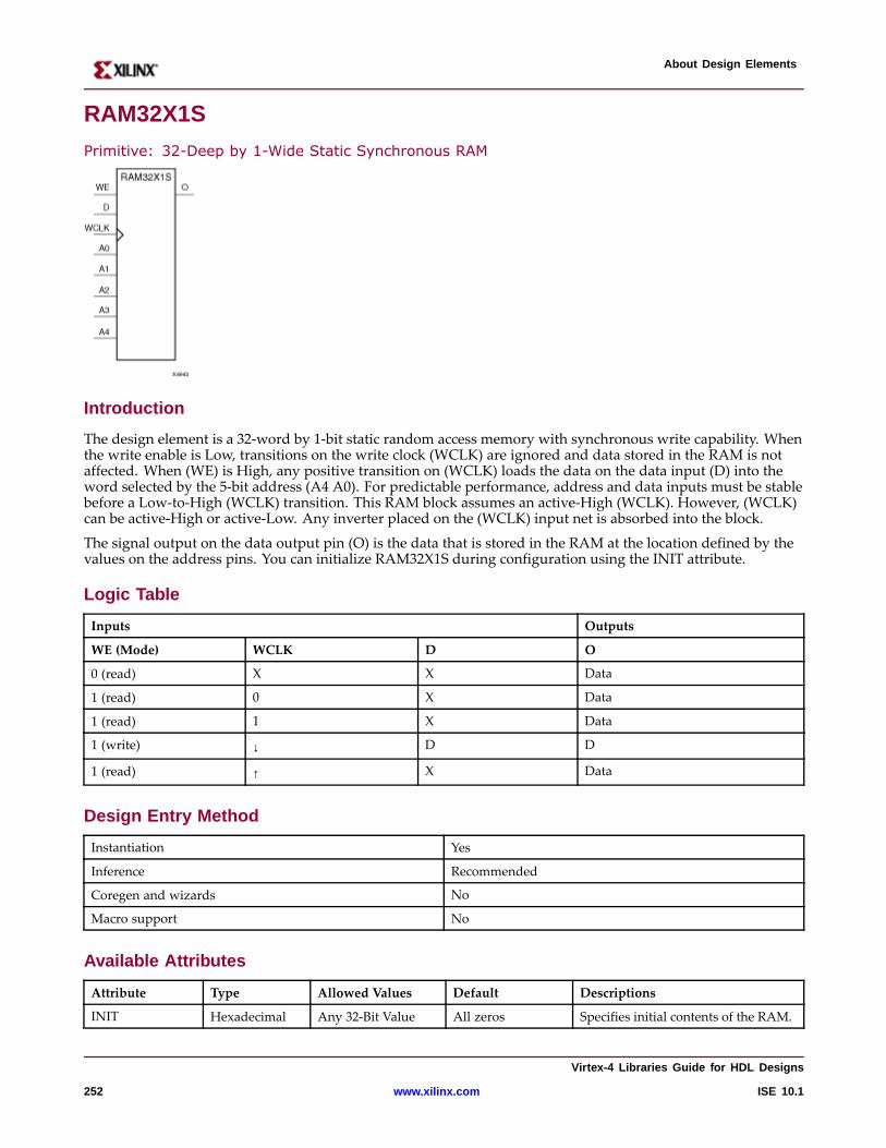
About Design Elements
RAM32X1S
Primitive: 32-Deep by 1-Wide Static Synchronous RAM
Intr oduction
The design element is a 32-word by 1-bit static random access memory with synchronous write capability. Whenthe write enable is Low, transitions on the write clock (WCLK) are ignored and data stored in the RAM is notaffected. When (WE) is High, any positive transition on (WCLK) loads the data on the data input (D) into theword selected by the 5-bit address (A4 A0). For predictable performance, address and data inputs must be stablebefore a Low-to-High (WCLK) transition. This RAM block assumes an active-High (WCLK). However, (WCLK)can be active-High or active-Low. Any inverter placed on the (WCLK) input net is absorbed into the block.
The signal output on the data output pin (O) is the data that is stored in the RAM at the location defined by thevalues on the address pins. You can initialize RAM32X1S during configuration using the INIT attribute.
Logic Table
Inputs Outputs
WE (Mode) WCLK D O
0 (read) X X Data
1 (read) 0 X Data
1 (read) 1 X Data
1 (write) ↓ D D
1 (read) ↑ X Data
Design Entr y Method
Instantiation Yes
Inference Recommended
Coregen and wizards No
Macro support No
Availab le Attrib utes
Attribute Type Allowed Values Default Descriptions
INIT Hexadecimal Any 32-Bit Value All zeros Specifies initial contents of the RAM.
Vir tex-4 Libraries Guide for HDL Designs
252 www.xilinx.com ISE 10.1
About Design Elements
VHDL Instantiation Template
Unless they already exist, copy the following two statements and paste them before the entity declaration.Library UNISIM;use UNISIM.vcomponents.all;
-- RAM32X1S: 32 x 1 posedge write distributed => LUT RAM-- All FPGA-- Xilinx HDL Libraries Guide, version 10.1.2
RAM32X1S_inst : RAM32X1Sgeneric map (INIT => X"00000000")port map (O => O, -- RAMoutputA0 => A0, -- RAMaddress[0] inputA1 => A1, -- RAMaddress[1] inputA2 => A2, -- RAMaddress[2] inputA3 => A3, -- RAMaddress[3] inputA4 => A4, -- RAMaddress[4] inputD => D, -- RAMdata inputWCLK=> WCLK, -- Write clock inputWE => WE -- Write enable input);
-- End of RAM32X1S_inst instantiation
Verilog Instantiation Template
// RAM32X1S: 32 x 1 posedge write distributed (LUT) RAM// All FPGA// Xilinx HDL Libraries Guide, version 10.1.2
RAM32X1S#(.INIT(32’h00000000) // Initial contents of RAM) RAM32X1S_inst (.O(O), // RAMoutput.A0(A0), // RAMaddress[0] input.A1(A1), // RAMaddress[1] input.A2(A2), // RAMaddress[2] input.A3(A3), // RAMaddress[3] input.A4(A4), // RAMaddress[4] input.D(D), // RAMdata input.WCLK(WCLK), // Write clock input.WE(WE) // Write enable input);
// End of RAM32X1S_inst instantiation
For More Information
• See the Virtex-4 User Guide.
• See the Virtex-4 Data Sheets.
Vir tex-4 Libraries Guide for HDL Designs
ISE 10.1 www.xilinx.com 253
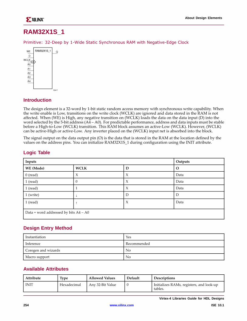
About Design Elements
RAM32X1S_1
Primitive: 32-Deep by 1-Wide Static Synchronous RAM with Negative-Edge Clock
Intr oduction
The design element is a 32-word by 1-bit static random access memory with synchronous write capability. Whenthe write enable is Low, transitions on the write clock (WCLK) are ignored and data stored in the RAM is notaffected. When (WE) is High, any negative transition on (WCLK) loads the data on the data input (D) into theword selected by the 5-bit address (A4 – A0). For predictable performance, address and data inputs must be stablebefore a High-to-Low (WCLK) transition. This RAM block assumes an active-Low (WCLK). However, (WCLK)can be active-High or active-Low. Any inverter placed on the (WCLK) input net is absorbed into the block.
The signal output on the data output pin (O) is the data that is stored in the RAM at the location defined by thevalues on the address pins. You can initialize RAM32X1S_1 during configuration using the INIT attribute.
Logic Table
Inputs Outputs
WE (Mode) WCLK D O
0 (read) X X Data
1 (read) 0 X Data
1 (read) 1 X Data
1 (write) ↓ D D
1 (read) ↑ X Data
Data = word addressed by bits A4 – A0
Design Entr y Method
Instantiation Yes
Inference Recommended
Coregen and wizards No
Macro support No
Availab le Attrib utes
Attribute Type Allowed Values Default Descriptions
INIT Hexadecimal Any 32-Bit Value 0 Initializes RAMs, registers, and look-uptables.
Vir tex-4 Libraries Guide for HDL Designs
254 www.xilinx.com ISE 10.1
About Design Elements
VHDL Instantiation Template
Unless they already exist, copy the following two statements and paste them before the entity declaration.Library UNISIM;use UNISIM.vcomponents.all;
-- RAM32X1S_1: 32 x 1 negedge write distributed => LUT RAM-- All FPGA-- Xilinx HDL Libraries Guide, version 10.1.2
RAM32X1S_1_inst : RAM32X1S_1generic map (INIT => X"00000000")port map (O => O, -- RAMoutputA0 => A0, -- RAMaddress[0] inputA1 => A1, -- RAMaddress[1] inputA2 => A2, -- RAMaddress[2] inputA3 => A3, -- RAMaddress[3] inputA4 => A4, -- RAMaddress[4] inputD => D, -- RAMdata inputWCLK=> WCLK, -- Write clock inputWE => WE -- Write enable input);
-- End of RAM32X1S_1_inst instantiation
Verilog Instantiation Template
// RAM32X1S_1: 32 x 1 negedge write distributed (LUT) RAM// Virtex/E/-II/-II-Pro, Spartan-II/IIE/3/3A// Xilinx HDL Libraries Guide, version 10.1.2
RAM32X1S_1 #(.INIT(32’h00000000) // Initial contents of RAM)RAM32X1S_1_inst (.O(O), // RAMoutput.A0(A0), // RAMaddress[0] input.A1(A1), // RAMaddress[1] input.A2(A2), // RAMaddress[2] input.A3(A3), // RAMaddress[3] input.A4(A4), // RAMaddress[4] input.D(D), // RAMdata input.WCLK(WCLK), // Write clock input.WE(WE) // Write enable input);
// End of RAM32X1S_1_inst instantiation
Vir tex-4 Libraries Guide for HDL Designs
ISE 10.1 www.xilinx.com 255

About Design Elements
For More Information
• See the Virtex-4 User Guide.
• See the Virtex-4 Data Sheets.
Vir tex-4 Libraries Guide for HDL Designs
256 www.xilinx.com ISE 10.1
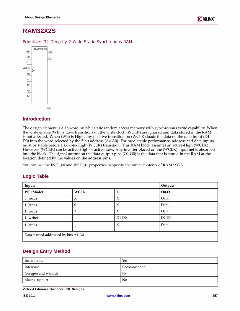
About Design Elements
RAM32X2S
Primitive: 32-Deep by 2-Wide Static Synchronous RAM
Intr oduction
The design element is a 32-word by 2-bit static random access memory with synchronous write capability. Whenthe write enable (WE) is Low, transitions on the write clock (WCLK) are ignored and data stored in the RAMis not affected. When (WE) is High, any positive transition on (WCLK) loads the data on the data input (D1D0) into the word selected by the 5-bit address (A4 A0). For predictable performance, address and data inputsmust be stable before a Low-to-High (WCLK) transition. This RAM block assumes an active-High (WCLK) .However, (WCLK) can be active-High or active-Low. Any inverter placed on the (WCLK) input net is absorbedinto the block. The signal output on the data output pins (O1 O0) is the data that is stored in the RAM at thelocation defined by the values on the address pins.
You can use the INIT_00 and INIT_01 properties to specify the initial contents of RAM32X2S.
Logic Table
Inputs Outputs
WE (Mode) WCLK D O0-O1
0 (read) X X Data
1 (read) 0 X Data
1 (read) 1 X Data
1 (write) ↑ D1-D0 D1-D0
1 (read) ↓ X Data
Data = word addressed by bits A4 A0
Design Entr y Method
Instantiation Yes
Inference Recommended
Coregen and wizards No
Macro support No
Vir tex-4 Libraries Guide for HDL Designs
ISE 10.1 www.xilinx.com 257
About Design Elements
Availab le Attrib utes
Attribute Type Allowed Values Default Descriptions
INIT_00 Hexadecimal Any 32-Bit Value All zeros INIT for bit 0 of RAM.
INIT_01 Hexadecimal Any 32-Bit Value All zeros INIT for bit 1 of RAM.
VHDL Instantiation Template
Unless they already exist, copy the following two statements and paste them before the entity declaration.Library UNISIM;use UNISIM.vcomponents.all;
-- RAM32X2S: 32 x 2 posedge write distributed => LUT RAM-- Virtex-II/II-Pro, Spartan-3/3E/3A-- Xilinx HDL Libraries Guide, version 10.1.2
RAM32X2S_inst : RAM32X2Sgeneric map (INIT_00 => X"00000000", -- INIT for bit 0 of RAMINIT_01 => X"00000000") -- INIT for bit 1 of RAMport map (O0 => O0, -- RAMdata[0] outputO1 => O1, -- RAMdata[1] outputA0 => A0, -- RAMaddress[0] inputA1 => A1, -- RAMaddress[1] inputA2 => A2, -- RAMaddress[2] inputA3 => A3, -- RAMaddress[3] inputA4 => A4, -- RAMaddress[4] inputD0 => D0, -- RAMdata[0] inputD1 => D1, -- RAMdata[1] inputWCLK=> WCLK, -- Write clock inputWE => WE -- Write enable input);
-- End of RAM32X2S_inst instantiation
Verilog Instantiation Template
// RAM32X2S: 32 x 2 posedge write distributed (LUT) RAM// Virtex-II/II-Pro, Spartan-3/3E/3A// Xilinx HDL Libraries Guide, version 10.1.2
RAM32X2S#(.INIT_00(32’h00000000), // INIT for bit 0 of RAM.INIT_01(32’h00000000) // INIT for bit 1 of RAM) RAM32X2S_inst (.O0(O0), // RAMdata[0] output.O1(O1), // RAMdata[1] output.A0(A0), // RAMaddress[0] input.A1(A1), // RAMaddress[1] input.A2(A2), // RAMaddress[2] input.A3(A3), // RAMaddress[3] input.A4(A4), // RAMaddress[4] input.D0(D0), // RAMdata[0] input.D1(D1), // RAMdata[1] input.WCLK(WCLK), // Write clock input.WE(WE) // Write enable input);
// End of RAM32X2S_inst instantiation
Vir tex-4 Libraries Guide for HDL Designs
258 www.xilinx.com ISE 10.1

About Design Elements
For More Information
• See the Virtex-4 User Guide.
• See the Virtex-4 Data Sheets.
Vir tex-4 Libraries Guide for HDL Designs
ISE 10.1 www.xilinx.com 259
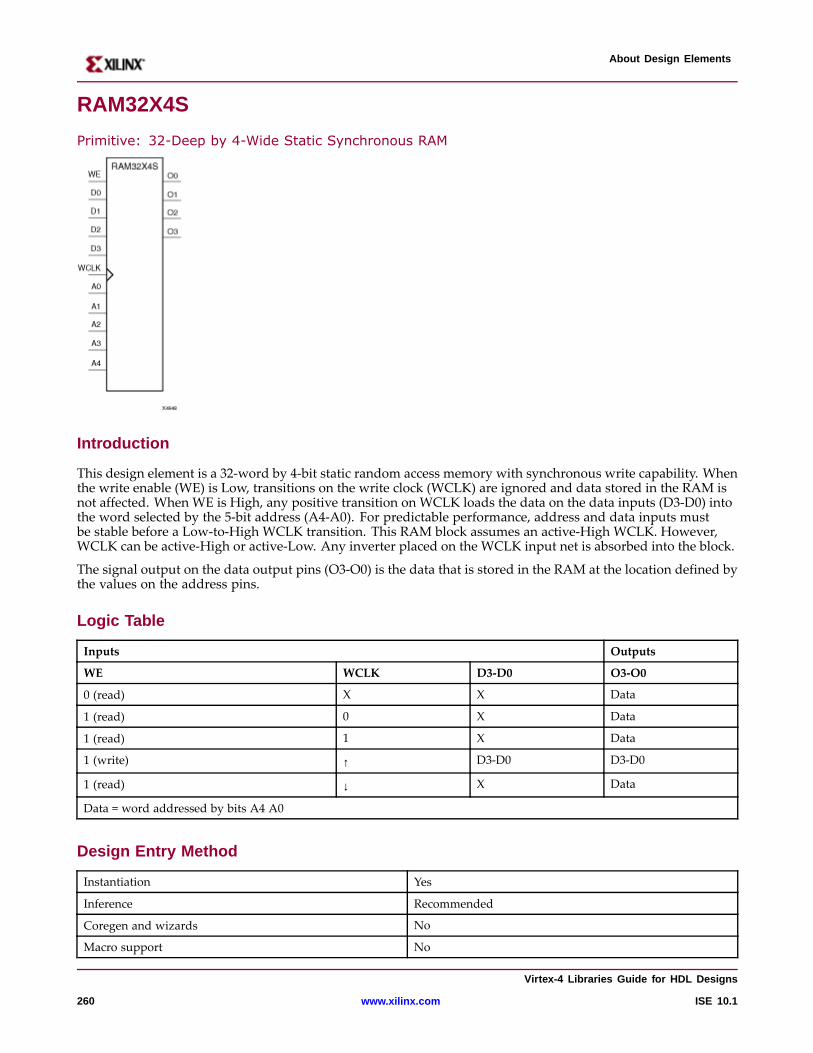
About Design Elements
RAM32X4S
Primitive: 32-Deep by 4-Wide Static Synchronous RAM
Intr oduction
This design element is a 32-word by 4-bit static random access memory with synchronous write capability. Whenthe write enable (WE) is Low, transitions on the write clock (WCLK) are ignored and data stored in the RAM isnot affected. When WE is High, any positive transition on WCLK loads the data on the data inputs (D3-D0) intothe word selected by the 5-bit address (A4-A0). For predictable performance, address and data inputs mustbe stable before a Low-to-High WCLK transition. This RAM block assumes an active-High WCLK. However,WCLK can be active-High or active-Low. Any inverter placed on the WCLK input net is absorbed into the block.
The signal output on the data output pins (O3-O0) is the data that is stored in the RAM at the location defined bythe values on the address pins.
Logic Table
Inputs Outputs
WE WCLK D3-D0 O3-O0
0 (read) X X Data
1 (read) 0 X Data
1 (read) 1 X Data
1 (write) ↑ D3-D0 D3-D0
1 (read) ↓ X Data
Data = word addressed by bits A4 A0
Design Entr y Method
Instantiation Yes
Inference Recommended
Coregen and wizards No
Macro support No
Vir tex-4 Libraries Guide for HDL Designs
260 www.xilinx.com ISE 10.1
About Design Elements
Availab le Attrib utes
Attribute Type Allowed Values Default Description
INIT_00 Hexadecimal Any 32-Bit Value All zeros INIT for bit 0 of RAM.
INIT_01 Hexadecimal Any 32-Bit Value All zeros INIT for bit 1 of RAM.
INIT_02 Hexadecimal Any 32-Bit Value All zeros INIT for bit 2 of RAM.
INIT_03 Hexadecimal Any 32-Bit Value All zeros INIT for bit 3 of RAM.
VHDL Instantiation Template
Unless they already exist, copy the following two statements and paste them before the entity declaration.Library UNISIM;use UNISIM.vcomponents.all;
-- RAM32X4S: 32 x 4 posedge write distributed => LUT RAM-- Virtex-II/II-Pro-- Xilinx HDL Libraries Guide, version 10.1.2
RAM32X4S_inst : RAM32X4Sgeneric map (INIT_00 => X"00000000", -- INIT for bit 0 of RAMINIT_01 => X"00000000", -- INIT for bit 1 of RAMINIT_02 => X"00000000", -- INIT for bit 2 of RAMINIT_03 => X"00000000") -- INIT for bit 3 of RAMport map (O0 => O0, -- RAMdata[0] outputO1 => O1, -- RAMdata[1] outputO2 => O2, -- RAMdata[2] outputO3 => O3, -- RAMdata[3] outputA0 => A0, -- RAMaddress[0] inputA1 => A1, -- RAMaddress[1] inputA2 => A2, -- RAMaddress[2] inputA3 => A3, -- RAMaddress[3] inputA4 => A4, -- RAMaddress[4] inputD0 => D0, -- RAMdata[0] inputD1 => D1, -- RAMdata[1] inputD2 => D2, -- RAMdata[2] inputD3 => D3, -- RAMdata[3] inputWCLK=> WCLK, -- Write clock inputWE => WE -- Write enable input);
-- End of RAM32X4S_inst instantiation
Verilog Instantiation Template
// RAM32X4S: 32 x 4 posedge write distributed (LUT) RAM// Virtex-II/II-Pro// Xilinx HDL Libraries Guide, version 10.1.2
RAM32X4S#(.INIT_00(32’h00000000), // INIT for bit 0 of RAM.INIT_01(32’h00000000), // INIT for bit 1 of RAM.INIT_02(32’h00000000), // INIT for bit 2 of RAM.INIT_03(32’h00000000) // INIT for bit 3 of RAM) RAM32X4S_inst (.O0(O0), // RAMdata[0] output.O1(O1), // RAMdata[1] output.O2(O2), // RAMdata[2] output.O3(O3), // RAMdata[3] output.A0(A0), // RAMaddress[0] input.A1(A1), // RAMaddress[1] input.A2(A2), // RAMaddress[2] input
Vir tex-4 Libraries Guide for HDL Designs
ISE 10.1 www.xilinx.com 261
About Design Elements
.A3(A3), // RAMaddress[3] input
.A4(A4), // RAMaddress[4] input
.D0(D0), // RAMdata[0] input
.D1(D1), // RAMdata[1] input
.D2(D2), // RAMdata[2] input
.D3(D3), // RAMdata[3] input
.WCLK(WCLK), // Write clock input
.WE(WE) // Write enable input);
// End of RAM32X4S_inst instantiation
For More Information
• See the Virtex-4 User Guide.
• See the Virtex-4 Data Sheets.
Vir tex-4 Libraries Guide for HDL Designs
262 www.xilinx.com ISE 10.1
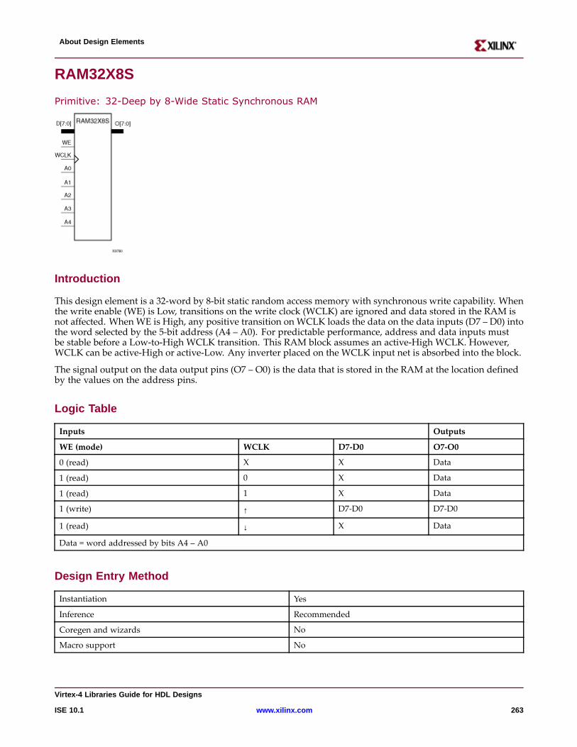
About Design Elements
RAM32X8S
Primitive: 32-Deep by 8-Wide Static Synchronous RAM
Intr oduction
This design element is a 32-word by 8-bit static random access memory with synchronous write capability. Whenthe write enable (WE) is Low, transitions on the write clock (WCLK) are ignored and data stored in the RAM isnot affected. When WE is High, any positive transition on WCLK loads the data on the data inputs (D7 – D0) intothe word selected by the 5-bit address (A4 – A0). For predictable performance, address and data inputs mustbe stable before a Low-to-High WCLK transition. This RAM block assumes an active-High WCLK. However,WCLK can be active-High or active-Low. Any inverter placed on the WCLK input net is absorbed into the block.
The signal output on the data output pins (O7 – O0) is the data that is stored in the RAM at the location definedby the values on the address pins.
Logic Table
Inputs Outputs
WE (mode) WCLK D7-D0 O7-O0
0 (read) X X Data
1 (read) 0 X Data
1 (read) 1 X Data
1 (write) ↑ D7-D0 D7-D0
1 (read) ↓ X Data
Data = word addressed by bits A4 – A0
Design Entr y Method
Instantiation Yes
Inference Recommended
Coregen and wizards No
Macro support No
Vir tex-4 Libraries Guide for HDL Designs
ISE 10.1 www.xilinx.com 263
About Design Elements
Availab le Attrib utes
Attribute Type Allowed Values Default Description
INIT_00 Hexadecimal Any 32-Bit Value All zeros INIT for bit 0 of RAM.
INIT_01 Hexadecimal Any 32-Bit Value All zeros INIT for bit 1 of RAM.
INIT_02 Hexadecimal Any 32-Bit Value All zeros INIT for bit 2 of RAM.
INIT_03 Hexadecimal Any 32-Bit Value All zeros INIT for bit 3 of RAM.
INIT_04 Hexadecimal Any 32-Bit Value All zeros INIT for bit 4 of RAM.
INIT_05 Hexadecimal Any 32-Bit Value All zeros INIT for bit 5 of RAM.
INIT_06 Hexadecimal Any 32-Bit Value All zeros INIT for bit 6 of RAM.
INIT_07 Hexadecimal Any 32-Bit Value All zeros INIT for bit 7 of RAM.
VHDL Instantiation Template
Unless they already exist, copy the following two statements and paste them before the entity declaration.Library UNISIM;use UNISIM.vcomponents.all;
-- RAM32X8S: 32 x 8 posedge write distributed => LUT RAM-- Virtex-II/II-Pro-- Xilinx HDL Libraries Guide, version 10.1.2
RAM32X8S_inst : RAM32X8Sgeneric map (INIT_00 => X"00000000", -- INIT for bit 0 of RAMINIT_01 => X"00000000", -- INIT for bit 1 of RAMINIT_02 => X"00000000", -- INIT for bit 2 of RAMINIT_03 => X"00000000", -- INIT for bit 3 of RAMINIT_04 => X"00000000", -- INIT for bit 4 of RAMINIT_05 => X"00000000", -- INIT for bit 5 of RAMINIT_06 => X"00000000", -- INIT for bit 6 of RAMINIT_07 => X"00000000") -- INIT for bit 7 of RAMport map (O => O, -- 8-bit RAMdata outputA0 => A0, -- RAMaddress[0] inputA1 => A1, -- RAMaddress[1] inputA2 => A2, -- RAMaddress[2] inputA3 => A3, -- RAMaddress[3] inputA4 => A4, -- RAMaddress[4] inputD => D, -- 8-bit RAMdata inputWCLK=> WCLK, -- Write clock inputWE => WE -- Write enable input);
-- End of RAM32X8S_inst instantiation
Verilog Instantiation Template
// RAM32X8S: 32 x 8 posedge write distributed (LUT) RAM// Virtex-II/II-Pro// Xilinx HDL Libraries Guide, version 10.1.2
RAM32X8S#(.INIT_00(32’h00000000), // INIT for bit 0 of RAM.INIT_01(32’h00000000), // INIT for bit 1 of RAM.INIT_02(32’h00000000), // INIT for bit 2 of RAM.INIT_03(32’h00000000), // INIT for bit 3 of RAM.INIT_04(32’h00000000), // INIT for bit 4 of RAM.INIT_05(32’h00000000), // INIT for bit 5 of RAM
Vir tex-4 Libraries Guide for HDL Designs
264 www.xilinx.com ISE 10.1
About Design Elements
.INIT_06(32’h00000000), // INIT for bit 6 of RAM
.INIT_07(32’h00000000) // INIT for bit 7 of RAM) RAM32X8S_inst (.O(O), // 8-bit RAMdata output.A0(A0), // RAMaddress[0] input.A1(A1), // RAMaddress[1] input.A2(A2), // RAMaddress[2] input.A3(A3), // RAMaddress[3] input.A4(A4), // RAMaddress[4] input.D(D), // 8-bit RAMdata input.WCLK(WCLK), // Write clock input.WE(WE) // Write enable input);
// End of RAM32X8S_inst instantiation
For More Information
• See the Virtex-4 User Guide.
• See the Virtex-4 Data Sheets.
Vir tex-4 Libraries Guide for HDL Designs
ISE 10.1 www.xilinx.com 265
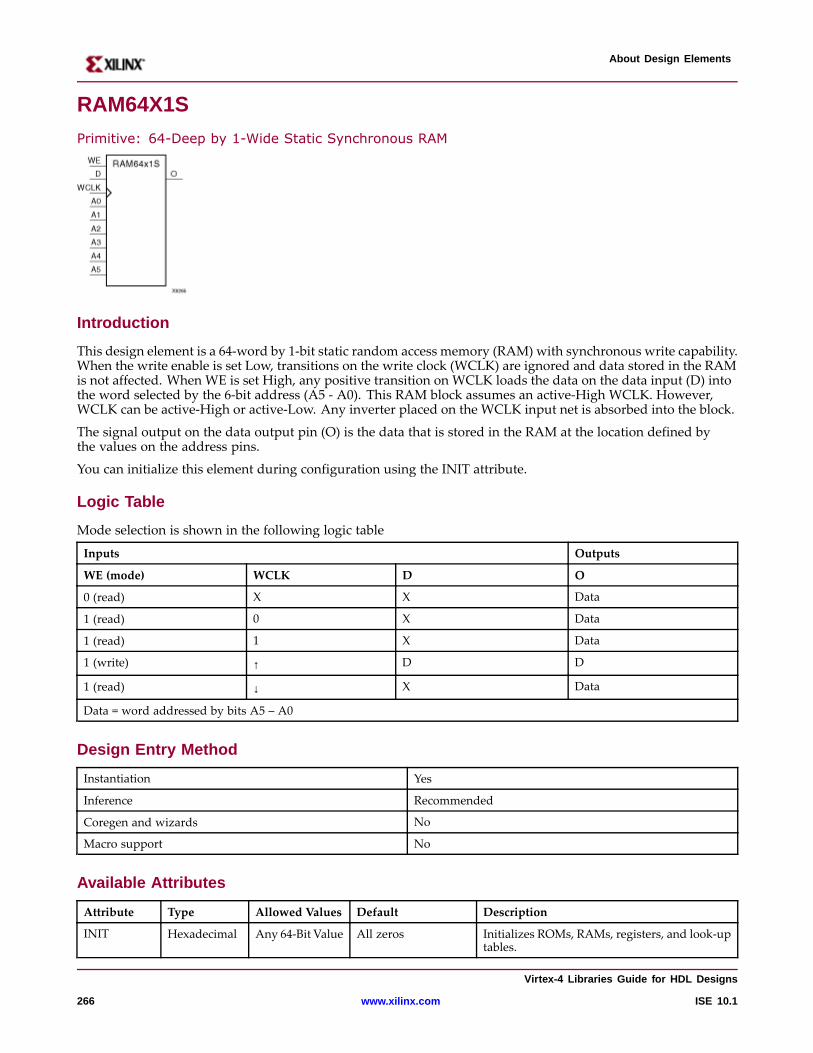
About Design Elements
RAM64X1S
Primitive: 64-Deep by 1-Wide Static Synchronous RAM
Intr oduction
This design element is a 64-word by 1-bit static random access memory (RAM) with synchronous write capability.When the write enable is set Low, transitions on the write clock (WCLK) are ignored and data stored in the RAMis not affected. When WE is set High, any positive transition on WCLK loads the data on the data input (D) intothe word selected by the 6-bit address (A5 - A0). This RAM block assumes an active-High WCLK. However,WCLK can be active-High or active-Low. Any inverter placed on the WCLK input net is absorbed into the block.
The signal output on the data output pin (O) is the data that is stored in the RAM at the location defined bythe values on the address pins.
You can initialize this element during configuration using the INIT attribute.
Logic Table
Mode selection is shown in the following logic table
Inputs Outputs
WE (mode) WCLK D O
0 (read) X X Data
1 (read) 0 X Data
1 (read) 1 X Data
1 (write) ↑ D D
1 (read) ↓ X Data
Data = word addressed by bits A5 – A0
Design Entr y Method
Instantiation Yes
Inference Recommended
Coregen and wizards No
Macro support No
Availab le Attrib utes
Attribute Type Allowed Values Default Description
INIT Hexadecimal Any 64-Bit Value All zeros Initializes ROMs, RAMs, registers, and look-uptables.
Vir tex-4 Libraries Guide for HDL Designs
266 www.xilinx.com ISE 10.1
About Design Elements
VHDL Instantiation Template
Unless they already exist, copy the following two statements and paste them before the entity declaration.Library UNISIM;use UNISIM.vcomponents.all;
-- RAM64X1S: 64 x 1 positive edge write, asynchronous read single-port distributed RAM-- Virtex-II/II-Pro/4/5, Spartan-3/3E/3A-- Xilinx HDL Libraries Guide, version 10.1.2
RAM64X1S_inst : RAM64X1Sgeneric map (INIT => X"0000000000000000")port map (O => O, -- 1-bit data outputA0 => A0, -- Address[0] input bitA1 => A1, -- Address[1] input bitA2 => A2, -- Address[2] input bitA3 => A3, -- Address[3] input bitA4 => A4, -- Address[4] input bitA5 => A5, -- Address[5] input bitD => D, -- 1-bit data inputWCLK=> WCLK, -- Write clock inputWE => WE -- Write enable input);
-- End of RAM64X1S_inst instantiation
Verilog Instantiation Template
// RAM64X1S: 64 x 1 positive edge write, asynchronous read single-port distributed RAM// Virtex-II/II-Pro/4/5, Spartan-3/3E/3A// Xilinx HDL Libraries Guide, version 10.1.2
RAM64X1S#(.INIT(64’h0000000000000000) // Initial contents of RAM) RAM64X1S_inst (.O(O), // 1-bit data output.A0(A0), // Address[0] input bit.A1(A1), // Address[1] input bit.A2(A2), // Address[2] input bit.A3(A3), // Address[3] input bit.A4(A4), // Address[4] input bit.A5(A5), // Address[5] input bit.D(D), // 1-bit data input.WCLK(WCLK), // Write clock input.WE(WE) // Write enable input);
// End of RAM64X1S_inst instantiation
Vir tex-4 Libraries Guide for HDL Designs
ISE 10.1 www.xilinx.com 267

About Design Elements
For More Information
• See the Virtex-4 User Guide.
• See the Virtex-4 Data Sheets.
Vir tex-4 Libraries Guide for HDL Designs
268 www.xilinx.com ISE 10.1
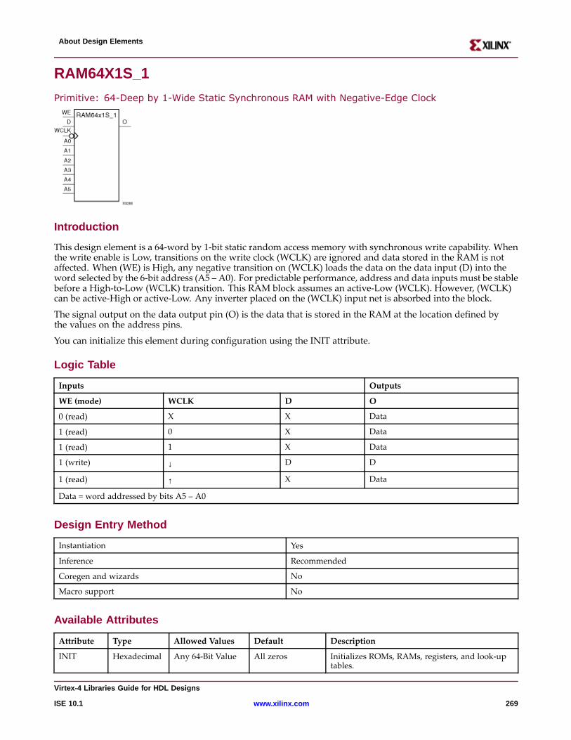
About Design Elements
RAM64X1S_1
Primitive: 64-Deep by 1-Wide Static Synchronous RAM with Negative-Edge Clock
Intr oduction
This design element is a 64-word by 1-bit static random access memory with synchronous write capability. Whenthe write enable is Low, transitions on the write clock (WCLK) are ignored and data stored in the RAM is notaffected. When (WE) is High, any negative transition on (WCLK) loads the data on the data input (D) into theword selected by the 6-bit address (A5 – A0). For predictable performance, address and data inputs must be stablebefore a High-to-Low (WCLK) transition. This RAM block assumes an active-Low (WCLK). However, (WCLK)can be active-High or active-Low. Any inverter placed on the (WCLK) input net is absorbed into the block.
The signal output on the data output pin (O) is the data that is stored in the RAM at the location defined bythe values on the address pins.
You can initialize this element during configuration using the INIT attribute.
Logic Table
Inputs Outputs
WE (mode) WCLK D O
0 (read) X X Data
1 (read) 0 X Data
1 (read) 1 X Data
1 (write) ↓ D D
1 (read) ↑ X Data
Data = word addressed by bits A5 – A0
Design Entr y Method
Instantiation Yes
Inference Recommended
Coregen and wizards No
Macro support No
Availab le Attrib utes
Attribute Type Allowed Values Default Description
INIT Hexadecimal Any 64-Bit Value All zeros Initializes ROMs, RAMs, registers, and look-uptables.
Vir tex-4 Libraries Guide for HDL Designs
ISE 10.1 www.xilinx.com 269
About Design Elements
VHDL Instantiation Template
Unless they already exist, copy the following two statements and paste them before the entity declaration.Library UNISIM;use UNISIM.vcomponents.all;
-- RAM64X1S_1: 64 x 1 negative edge write, asynchronous read single-port distributed RAM-- Virtex-II/II-Pro, Spartan-3/3E/3A-- Xilinx HDL Libraries Guide, version 10.1.2
RAM64X1S_1_inst : RAM64X1S_1generic map (INIT => X"0000000000000000")port map (O => O, -- 1-bit data outputA0 => A0, -- Address[0] input bitA1 => A1, -- Address[1] input bitA2 => A2, -- Address[2] input bitA3 => A3, -- Address[3] input bitA4 => A4, -- Address[4] input bitA5 => A5, -- Address[5] input bitD => D, -- 1-bit data inputWCLK=> WCLK, -- Write clock inputWE => WE -- Write enable input);
-- End of RAM64X1S_1_inst instantiation
Verilog Instantiation Template
// RAM64X1S_1: 64 x 1 negative edge write, asynchronous read single-port distributed RAM// Virtex-II/II-Pro, Spartan-3/3E/3A// Xilinx HDL Libraries Guide, version 10.1.2
RAM64X1S_1 #(.INIT(64’h0000000000000000) // Initial contents of RAM) RAM64X1S_1_inst (.O(O), // 1-bit data output.A0(A0), // Address[0] input bit.A1(A1), // Address[1] input bit.A2(A2), // Address[2] input bit.A3(A3), // Address[3] input bit.A4(A4), // Address[4] input bit.A5(A5), // Address[5] input bit.D(D), // 1-bit data input.WCLK(WCLK), // Write clock input.WE(WE) // Write enable input);
// End of RAM64X1S_1_inst instantiation
For More Information
• See the Virtex-4 User Guide.
• See the Virtex-4 Data Sheets.
Vir tex-4 Libraries Guide for HDL Designs
270 www.xilinx.com ISE 10.1

About Design Elements
RAM64X2S
Primitive: 64-Deep by 2-Wide Static Synchronous RAM
Intr oduction
This design element is a 64-word by 2-bit static random access memory with synchronous write capability. Whenthe write enable (WE) is Low, transitions on the write clock (WCLK) are ignored and data stored in the RAM isnot affected. When WE is High, any positive transition on WCLK loads the data on the data input (D1 – D0) intothe word selected by the 6-bit address (A5 – A0). For predictable performance, address and data inputs mustbe stable before a Low-to-High WCLK transition. This RAM block assumes an active-High WCLK. However,WCLK can be active-High or active-Low. Any inverter placed on the WCLK input net is absorbed into the block.
The signal output on the data output pins (O1 – O0) is the data that is stored in the RAM at the location definedby the values on the address pins. You can use the INIT_00 and INIT_01 properties to specify the initial contentsof this design element.
Logic Table
Inputs Outputs
WE (mode) WCLK D0-D1 O0-O1
0 (read) X X Data
1 (read) 0 X Data
1 (read) 1 X Data
1 (write) ↑ D1-D0 D1-D0
1 (read) ↓ X Data
Data = word addressed by bits A5 – A0
Design Entr y Method
Instantiation Yes
Inference Recommended
Coregen and wizards No
Macro support No
Vir tex-4 Libraries Guide for HDL Designs
ISE 10.1 www.xilinx.com 271
About Design Elements
Availab le Attrib utes
Attribute Type Allowed Values Default Description
INIT_00 Hexadecimal Any 64-Bit Value All zeros Initializes RAMs, registers, and look-uptables.
INIT_01 Hexadecimal Any 64-Bit Value All zeros Initializes RAMs, registers, and look-uptables.
VHDL Instantiation Template
Unless they already exist, copy the following two statements and paste them before the entity declaration.Library UNISIM;use UNISIM.vcomponents.all;
-- RAM64X2S: 64 x 2 positive edge write, asynchronous read single-port distributed RAM-- Virtex-II/II-Pro/4/5-- Xilinx HDL Libraries Guide, version 10.1.2
RAM64X2S_inst : RAM64X2Sgeneric map (INIT_00 => X"0000000000000000", -- INIT for bit 0 of RAMINIT_01 => X"0000000000000000") -- INIT for bit 1 of RAMport map (O0 => O0, -- Data[0] outputO1 => O1, -- Data[1] output bitA0 => A0, -- Address[0] input bitA1 => A1, -- Address[1] input bitA2 => A2, -- Address[2] input bitA3 => A3, -- Address[3] input bitA4 => A4, -- Address[4] input bitA5 => A5, -- Address[5] input bitD0 => D0, -- Data[0] inputD1 => D1, -- Data[1] inputWCLK=> WCLK, -- Write clock inputWE => WE -- Write enable input);
-- End of RAM64X2S_inst instantiation
Verilog Instantiation Template
// RAM64X2S: 64 x 2 positive edge write, asynchronous read single-port distributed RAM// Virtex-II/II-Pro// Xilinx HDL Libraries Guide, version 10.1.2
RAM64X2S#(.INIT_00(64’h0000000000000000), // INIT for RAMbit 0.INIT_01(64’h0000000000000000) // INIT for RAMbit 1) RAM64X2S_inst (.O0(O0), // Data[0] output.O1(O1), // Data[1] output bit.A0(A0), // Address[0] input bit.A1(A1), // Address[1] input bit.A2(A2), // Address[2] input bit.A3(A3), // Address[3] input bit.A4(A4), // Address[4] input bit.A5(A5), // Address[5] input bit.D0(D0), // Data[0] input.D1(D1), // Data[1] input.WCLK(WCLK), // Write clock input.WE(WE) // Write enable input);
// End of RAM64X2S_inst instantiation
Vir tex-4 Libraries Guide for HDL Designs
272 www.xilinx.com ISE 10.1

About Design Elements
For More Information
• See the Virtex-4 User Guide.
• See the Virtex-4 Data Sheets.
Vir tex-4 Libraries Guide for HDL Designs
ISE 10.1 www.xilinx.com 273
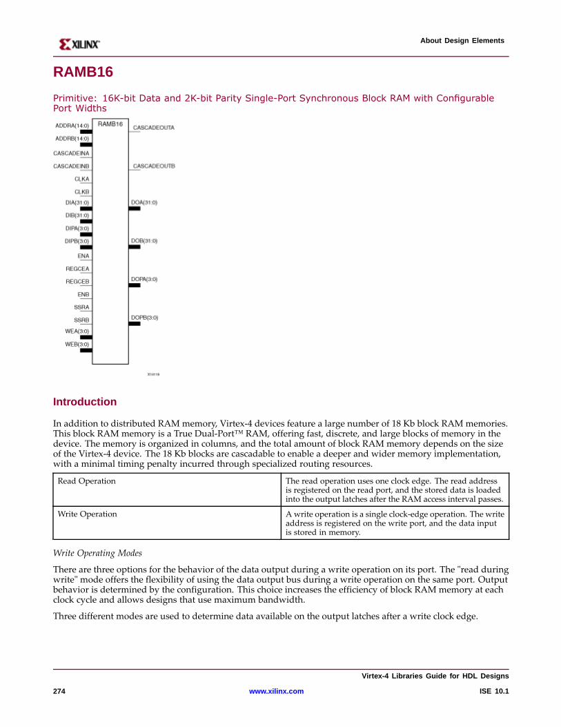
About Design Elements
RAMB16
Primitive: 16K-bit Data and 2K-bit Parity Single-Port Synchronous Block RAM with ConfigurablePort Widths
Intr oduction
In addition to distributed RAMmemory, Virtex-4 devices feature a large number of 18 Kb block RAMmemories.This block RAM memory is a True Dual-Port™ RAM, offering fast, discrete, and large blocks of memory in thedevice. The memory is organized in columns, and the total amount of block RAM memory depends on the sizeof the Virtex-4 device. The 18 Kb blocks are cascadable to enable a deeper and wider memory implementation,with a minimal timing penalty incurred through specialized routing resources.
Read Operation The read operation uses one clock edge. The read addressis registered on the read port, and the stored data is loadedinto the output latches after the RAM access interval passes.
Write Operation A write operation is a single clock-edge operation. The writeaddress is registered on the write port, and the data inputis stored in memory.
Write Operating Modes
There are three options for the behavior of the data output during a write operation on its port. The "read duringwrite" mode offers the flexibility of using the data output bus during a write operation on the same port. Outputbehavior is determined by the configuration. This choice increases the efficiency of block RAM memory at eachclock cycle and allows designs that use maximum bandwidth.
Three different modes are used to determine data available on the output latches after a write clock edge.
Vir tex-4 Libraries Guide for HDL Designs
274 www.xilinx.com ISE 10.1
About Design Elements
WRITE_FIRST or Transparent Mode (Default) The input data is simultaneously written into memory andstored in the data output (transparent write)
READ_FIRST or Read-Before-Write Mode Data previously stored at the write address appears onthe output latches, while the input data is being stored inmemory (read before write).
NO_CHANGE Mode The output latches remain unchanged during a writeoperation.
Mode selection is set by configuration. One of these three modes is set individually for each port by an attribute.The default mode is WRITE_FIRST.
Por t Descriptions
Output Latches Synchronous Set/Reset - SRVAL (SRVAL_A & SRVAL_B)
The SRVAL_A and SRVAL_B (dual-port) attributes define output latch values when the SSR input is asserted.The width of the SRVAL (SRVAL_A and SRVAL_B) attribute is the port width, as shown in the following table:
Port Width Values andData Width DOP Bus DO Bus SRVAL
1 NA <0> 1
2 NA <1:0> 2
4 NA <3:0> 4
9 <0> <7:0> (1+8) = 9
18 <1:0> <15:0> (2+16) = 18
36 <3:0> <31:0> (4 + 32) = 36
Optional Output Register On/Off Switch - DO[A/B]_REG
This attribute sets the number of pipeline register at A/B output of RAMB16. The valid values are 0 (default) or 1.
Clock Inversion at Output Register Switch - INVERT_CLK_DO[A/B]_REG
When set to TRUE, the clock input to the pipeline register at A/B output of RAMB16 is inverted. The defaultvalue is FALSE.
Extended Mode Address Determinant - RAM_EXTENSION_[A/B]
This attribute determines whether the block RAM of interest has its A/B port as UPPER/LOWER address whenusing the cascade mode. In the cascading mode, READ_WIDTH_[A/B] and WRITE_WIDTH_[A/B] should be setto 1. When the block RAM is not used in cascade mode, the default value is NONE.
Read Width - READ_WIDTH_[A/B]
This attribute determines the A/B read port width of the block RAM. The valid values are: 0 (default), 1, 2, 4, 9,18, and 36. The READ_WIDTH_[A/B] for both the ports should not be set to zero at the same time.
Write Width - WRITE_WIDTH_[A/B]
This attribute determines the A/B write port width of the block RAM. The valid values are: 0 (default), 1, 2, 4, 9,18, and 36.
Write Mode - WRITE_MODE_[A/B]
This attribute determines the write mode of the A/B input ports. The possible values are WRITE_FIRST (default),READ_FIRST, and NO_CHANGE.
RAMB16 Location Constraints
Block RAM instances can have LOC properties attached to them to constrain placement. Block RAM placementlocations differ from the convention used for naming CLB locations, allowing LOC properties to transfer easilyfrom array to array. The LOC properties use the following form: LOC = RAMB16_X#Y#
Vir tex-4 Libraries Guide for HDL Designs
ISE 10.1 www.xilinx.com 275
About Design Elements
The RAMB16_X0Y0 is the bottom-left block RAM location on the device.
Design Entr y Method
Instantiation Yes
Inference Recommended
Coregen and wizards Yes
Macro support No
Availab le Attrib utes
Attribute Type Allowed Values Default Description
DOA_REG Integer 0 or 1 0 Optional output registers on Aport .
DOB_REG Integer 0 or 1 0 Optional output registers on Bport.
INIT_00 to INIT_39 Hexadecimal Any 256-Bit Value All zeros To change the initial contents ofthe RAM to anything other thanall zero’s.
INIT_0A to INIT_0F Hexadecimal Any 256-Bit Value All zeros To change the initial contents ofthe RAM to anything other thanall zero’s.
INIT_1A to INIT_1F Hexadecimal Any 256-Bit Value All zeros To change the initial contents ofthe RAM to anything other thanall zero’s.
INIT_2A to INIT_2F Hexadecimal Any 256-Bit Value All zeros To change the initial contents ofthe RAM to anything other thanall zero’s.
INIT_3A to INIT_3F Hexadecimal Any 256-Bit Value All zeros To change the initial contents ofthe RAM to anything other thanall zero’s.
INIT_A Hexadecimal Any 36-Bit Value All zeros Initial values on A output port.
INIT_B Hexadecimal Any 36-Bit Value All zeros Initial values on B output port.
INITP_00 to INITP_07 Hexadecimal Any 256-Bit Value All zeros Applied for the parity bits.
INVERT_CLK_DOA_REG
Boolean FALSE, TRUE FALSE Invert clock on A port outputregisters.
INVERT_CLK_DOB_REG
Boolean FALSE, TRUE FALSE Invert clock on A port outputregisters.
RAM_EXTENSION_A String "LOWER", "NONE"or "UPPER”
"NONE” Allowed value when cascaded.
RAM_EXTENSION_B String "LOWER", "NONE"or "UPPER”
"NONE” Allowed value when cascaded.
READ_WIDTH_A Integer 0, 1, 2, 4, 9, 18 or 36 0 Set/Reset for the allowed value.
READ_WIDTH_B Integer 0, 1, 2, 4, 9, 18 or 36 0 Set/Reset for the allowed value.
SIM_COLLISION_CHECK
String "ALL", "NONE" or"GENERATE_X_ONLY”
"ALL” Collision check enable for theallowed value.
SRVAL_A Hexadecimal Any 36-Bit Value. All zeros Use to set/reset value for A portoutput.
Vir tex-4 Libraries Guide for HDL Designs
276 www.xilinx.com ISE 10.1
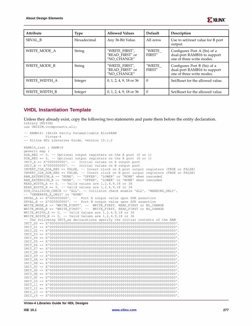
About Design Elements
Attribute Type Allowed Values Default Description
SRVAL_B Hexadecimal Any 36-Bit Value. All zeros Use to set/reset value for B portoutput.
WRITE_MODE_A String "WRITE_FIRST","READ_FIRST" or"NO_CHANGE”
"WRITE_FIRST”
Configures Port A (Sn) of adual-port RAMB16 to supportone of three write modes.
WRITE_MODE_B String "WRITE_FIRST","READ_FIRST" or"NO_CHANGE”
"WRITE_FIRST”
Configures Port B (Sn) of adual-port RAMB16 to supportone of three write modes.
WRITE_WIDTH_A Integer 0, 1, 2, 4, 9, 18 or 36 0 Set/Reset for the allowed value.
WRITE_WIDTH_B Integer 0, 1, 2, 4, 9, 18 or 36 0 Set/Reset for the allowed value.
VHDL Instantiation Template
Unless they already exist, copy the following two statements and paste them before the entity declaration.Library UNISIM;use UNISIM.vcomponents.all;
-- RAMB16: 16k+2k Parity Paramatizable BlockRAM-- Virtex-4-- Xilinx HDL Libraries Guide, version 10.1.2
RAMB16_inst : RAMB16generic map (DOA_REG=> 0, -- Optional output registers on the A port (0 or 1)DOB_REG=> 0, -- Optional output registers on the B port (0 or 1)INIT_A => X"000000000", -- Initial values on A output portINIT_B => X"000000000", -- Initial values on B output portINVERT_CLK_DOA_REG=> FALSE, -- Invert clock on A port output registers (TRUE or FALSE)INVERT_CLK_DOB_REG=> FALSE, -- Invert clock on B port output registers (TRUE or FALSE)RAM_EXTENSION_A=> "NONE", -- "UPPER", "LOWER" or "NONE" when cascadedRAM_EXTENSION_B=> "NONE", -- "UPPER", "LOWER" or "NONE" when cascadedREAD_WIDTH_A=> 0, -- Valid values are 1,2,4,9,18 or 36READ_WIDTH_B=> 0, -- Valid values are 1,2,4,9,18 or 36SIM_COLLISION_CHECK => "ALL", -- Collision check enable "ALL", "WARNING_ONLY",-- "GENERATE_X_ONLY"or "NONE"SRVAL_A => X"000000000", -- Port A output value upon SSR assertionSRVAL_B => X"000000000", -- Port B output value upon SSR assertionWRITE_MODE_A=> "WRITE_FIRST", -- WRITE_FIRST, READ_FIRST or NO_CHANGEWRITE_MODE_B=> "WRITE_FIRST", -- WRITE_FIRST, READ_FIRST or NO_CHANGEWRITE_WIDTH_A=> 0, -- Valid values are 1,2,4,9,18 or 36WRITE_WIDTH_B=> 0, -- Valid values are 1,2,4,9,18 or 36-- The following INIT_xx declarations specify the initial contents of the RAMINIT_00 => X"0000000000000000000000000000000000000000000000000000000000000000",INIT_01 => X"0000000000000000000000000000000000000000000000000000000000000000",INIT_02 => X"0000000000000000000000000000000000000000000000000000000000000000",INIT_03 => X"0000000000000000000000000000000000000000000000000000000000000000",INIT_04 => X"0000000000000000000000000000000000000000000000000000000000000000",INIT_05 => X"0000000000000000000000000000000000000000000000000000000000000000",INIT_06 => X"0000000000000000000000000000000000000000000000000000000000000000",INIT_07 => X"0000000000000000000000000000000000000000000000000000000000000000",INIT_08 => X"0000000000000000000000000000000000000000000000000000000000000000",INIT_09 => X"0000000000000000000000000000000000000000000000000000000000000000",INIT_0A => X"0000000000000000000000000000000000000000000000000000000000000000",INIT_0B => X"0000000000000000000000000000000000000000000000000000000000000000",INIT_0C => X"0000000000000000000000000000000000000000000000000000000000000000",INIT_0D => X"0000000000000000000000000000000000000000000000000000000000000000",INIT_0E => X"0000000000000000000000000000000000000000000000000000000000000000",INIT_0F => X"0000000000000000000000000000000000000000000000000000000000000000",INIT_10 => X"0000000000000000000000000000000000000000000000000000000000000000",INIT_11 => X"0000000000000000000000000000000000000000000000000000000000000000",INIT_12 => X"0000000000000000000000000000000000000000000000000000000000000000",INIT_13 => X"0000000000000000000000000000000000000000000000000000000000000000",INIT_14 => X"0000000000000000000000000000000000000000000000000000000000000000",
Vir tex-4 Libraries Guide for HDL Designs
ISE 10.1 www.xilinx.com 277
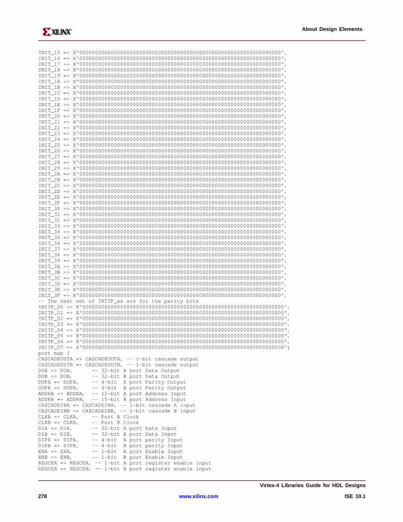
About Design Elements
INIT_15 => X"0000000000000000000000000000000000000000000000000000000000000000",INIT_16 => X"0000000000000000000000000000000000000000000000000000000000000000",INIT_17 => X"0000000000000000000000000000000000000000000000000000000000000000",INIT_18 => X"0000000000000000000000000000000000000000000000000000000000000000",INIT_19 => X"0000000000000000000000000000000000000000000000000000000000000000",INIT_1A => X"0000000000000000000000000000000000000000000000000000000000000000",INIT_1B => X"0000000000000000000000000000000000000000000000000000000000000000",INIT_1C => X"0000000000000000000000000000000000000000000000000000000000000000",INIT_1D => X"0000000000000000000000000000000000000000000000000000000000000000",INIT_1E => X"0000000000000000000000000000000000000000000000000000000000000000",INIT_1F => X"0000000000000000000000000000000000000000000000000000000000000000",INIT_20 => X"0000000000000000000000000000000000000000000000000000000000000000",INIT_21 => X"0000000000000000000000000000000000000000000000000000000000000000",INIT_22 => X"0000000000000000000000000000000000000000000000000000000000000000",INIT_23 => X"0000000000000000000000000000000000000000000000000000000000000000",INIT_24 => X"0000000000000000000000000000000000000000000000000000000000000000",INIT_25 => X"0000000000000000000000000000000000000000000000000000000000000000",INIT_26 => X"0000000000000000000000000000000000000000000000000000000000000000",INIT_27 => X"0000000000000000000000000000000000000000000000000000000000000000",INIT_28 => X"0000000000000000000000000000000000000000000000000000000000000000",INIT_29 => X"0000000000000000000000000000000000000000000000000000000000000000",INIT_2A => X"0000000000000000000000000000000000000000000000000000000000000000",INIT_2B => X"0000000000000000000000000000000000000000000000000000000000000000",INIT_2C => X"0000000000000000000000000000000000000000000000000000000000000000",INIT_2D => X"0000000000000000000000000000000000000000000000000000000000000000",INIT_2E => X"0000000000000000000000000000000000000000000000000000000000000000",INIT_2F => X"0000000000000000000000000000000000000000000000000000000000000000",INIT_30 => X"0000000000000000000000000000000000000000000000000000000000000000",INIT_31 => X"0000000000000000000000000000000000000000000000000000000000000000",INIT_32 => X"0000000000000000000000000000000000000000000000000000000000000000",INIT_33 => X"0000000000000000000000000000000000000000000000000000000000000000",INIT_34 => X"0000000000000000000000000000000000000000000000000000000000000000",INIT_35 => X"0000000000000000000000000000000000000000000000000000000000000000",INIT_36 => X"0000000000000000000000000000000000000000000000000000000000000000",INIT_37 => X"0000000000000000000000000000000000000000000000000000000000000000",INIT_38 => X"0000000000000000000000000000000000000000000000000000000000000000",INIT_39 => X"0000000000000000000000000000000000000000000000000000000000000000",INIT_3A => X"0000000000000000000000000000000000000000000000000000000000000000",INIT_3B => X"0000000000000000000000000000000000000000000000000000000000000000",INIT_3C => X"0000000000000000000000000000000000000000000000000000000000000000",INIT_3D => X"0000000000000000000000000000000000000000000000000000000000000000",INIT_3E => X"0000000000000000000000000000000000000000000000000000000000000000",INIT_3F => X"0000000000000000000000000000000000000000000000000000000000000000",-- The next set of INITP_xx are for the parity bitsINITP_00 => X"0000000000000000000000000000000000000000000000000000000000000000",INITP_01 => X"0000000000000000000000000000000000000000000000000000000000000000",INITP_02 => X"0000000000000000000000000000000000000000000000000000000000000000",INITP_03 => X"0000000000000000000000000000000000000000000000000000000000000000",INITP_04 => X"0000000000000000000000000000000000000000000000000000000000000000",INITP_05 => X"0000000000000000000000000000000000000000000000000000000000000000",INITP_06 => X"0000000000000000000000000000000000000000000000000000000000000000",INITP_07 => X"0000000000000000000000000000000000000000000000000000000000000000")port map (CASCADEOUTA=> CASCADEOUTA,-- 1-bit cascade outputCASCADEOUTB=> CASCADEOUTB,-- 1-bit cascade outputDOA => DOA, -- 32-bit A port Data OutputDOB => DOB, -- 32-bit B port Data OutputDOPA=> DOPA, -- 4-bit A port Parity OutputDOPB=> DOPB, -- 4-bit B port Parity OutputADDRA=> ADDRA, -- 15-bit A port Address InputADDRB=> ADDRB, -- 15-bit B port Address InputCASCADEINA=> CASCADEINA, -- 1-bit cascade A inputCASCADEINB=> CASCADEINB, -- 1-bit cascade B inputCLKA => CLKA, -- Port A ClockCLKB => CLKB, -- Port B ClockDIA => DIA, -- 32-bit A port Data InputDIB => DIB, -- 32-bit B port Data InputDIPA => DIPA, -- 4-bit A port parity InputDIPB => DIPB, -- 4-bit B port parity InputENA => ENA, -- 1-bit A port Enable InputENB => ENB, -- 1-bit B port Enable InputREGCEA=> REGCEA, -- 1-bit A port register enable inputREGCEB=> REGCEB, -- 1-bit B port register enable input
Vir tex-4 Libraries Guide for HDL Designs
278 www.xilinx.com ISE 10.1
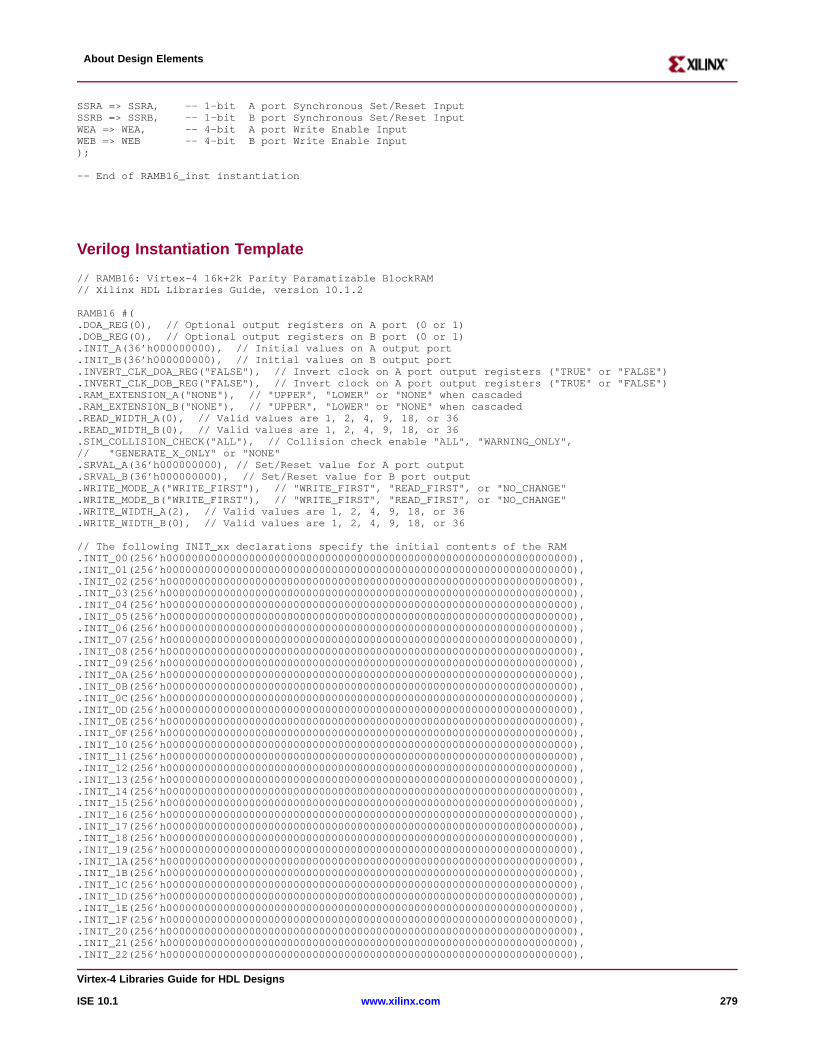
About Design Elements
SSRA => SSRA, -- 1-bit A port Synchronous Set/Reset InputSSRB => SSRB, -- 1-bit B port Synchronous Set/Reset InputWEA=> WEA, -- 4-bit A port Write Enable InputWEB=> WEB -- 4-bit B port Write Enable Input);
-- End of RAMB16_inst instantiation
Verilog Instantiation Template
// RAMB16: Virtex-4 16k+2k Parity Paramatizable BlockRAM// Xilinx HDL Libraries Guide, version 10.1.2
RAMB16 #(.DOA_REG(0), // Optional output registers on A port (0 or 1).DOB_REG(0), // Optional output registers on B port (0 or 1).INIT_A(36’h000000000), // Initial values on A output port.INIT_B(36’h000000000), // Initial values on B output port.INVERT_CLK_DOA_REG("FALSE"), // Invert clock on A port output registers ("TRUE" or "FALSE").INVERT_CLK_DOB_REG("FALSE"), // Invert clock on A port output registers ("TRUE" or "FALSE").RAM_EXTENSION_A("NONE"), // "UPPER", "LOWER" or "NONE" when cascaded.RAM_EXTENSION_B("NONE"), // "UPPER", "LOWER" or "NONE" when cascaded.READ_WIDTH_A(0), // Valid values are 1, 2, 4, 9, 18, or 36.READ_WIDTH_B(0), // Valid values are 1, 2, 4, 9, 18, or 36.SIM_COLLISION_CHECK("ALL"), // Collision check enable "ALL", "WARNING_ONLY",// "GENERATE_X_ONLY"or "NONE".SRVAL_A(36’h000000000), // Set/Reset value for A port output.SRVAL_B(36’h000000000), // Set/Reset value for B port output.WRITE_MODE_A("WRITE_FIRST"), // "WRITE_FIRST", "READ_FIRST", or "NO_CHANGE".WRITE_MODE_B("WRITE_FIRST"), // "WRITE_FIRST", "READ_FIRST", or "NO_CHANGE".WRITE_WIDTH_A(2), // Valid values are 1, 2, 4, 9, 18, or 36.WRITE_WIDTH_B(0), // Valid values are 1, 2, 4, 9, 18, or 36
// The following INIT_xx declarations specify the initial contents of the RAM.INIT_00(256’h0000000000000000000000000000000000000000000000000000000000000000),.INIT_01(256’h0000000000000000000000000000000000000000000000000000000000000000),.INIT_02(256’h0000000000000000000000000000000000000000000000000000000000000000),.INIT_03(256’h0000000000000000000000000000000000000000000000000000000000000000),.INIT_04(256’h0000000000000000000000000000000000000000000000000000000000000000),.INIT_05(256’h0000000000000000000000000000000000000000000000000000000000000000),.INIT_06(256’h0000000000000000000000000000000000000000000000000000000000000000),.INIT_07(256’h0000000000000000000000000000000000000000000000000000000000000000),.INIT_08(256’h0000000000000000000000000000000000000000000000000000000000000000),.INIT_09(256’h0000000000000000000000000000000000000000000000000000000000000000),.INIT_0A(256’h0000000000000000000000000000000000000000000000000000000000000000),.INIT_0B(256’h0000000000000000000000000000000000000000000000000000000000000000),.INIT_0C(256’h0000000000000000000000000000000000000000000000000000000000000000),.INIT_0D(256’h0000000000000000000000000000000000000000000000000000000000000000),.INIT_0E(256’h0000000000000000000000000000000000000000000000000000000000000000),.INIT_0F(256’h0000000000000000000000000000000000000000000000000000000000000000),.INIT_10(256’h0000000000000000000000000000000000000000000000000000000000000000),.INIT_11(256’h0000000000000000000000000000000000000000000000000000000000000000),.INIT_12(256’h0000000000000000000000000000000000000000000000000000000000000000),.INIT_13(256’h0000000000000000000000000000000000000000000000000000000000000000),.INIT_14(256’h0000000000000000000000000000000000000000000000000000000000000000),.INIT_15(256’h0000000000000000000000000000000000000000000000000000000000000000),.INIT_16(256’h0000000000000000000000000000000000000000000000000000000000000000),.INIT_17(256’h0000000000000000000000000000000000000000000000000000000000000000),.INIT_18(256’h0000000000000000000000000000000000000000000000000000000000000000),.INIT_19(256’h0000000000000000000000000000000000000000000000000000000000000000),.INIT_1A(256’h0000000000000000000000000000000000000000000000000000000000000000),.INIT_1B(256’h0000000000000000000000000000000000000000000000000000000000000000),.INIT_1C(256’h0000000000000000000000000000000000000000000000000000000000000000),.INIT_1D(256’h0000000000000000000000000000000000000000000000000000000000000000),.INIT_1E(256’h0000000000000000000000000000000000000000000000000000000000000000),.INIT_1F(256’h0000000000000000000000000000000000000000000000000000000000000000),.INIT_20(256’h0000000000000000000000000000000000000000000000000000000000000000),.INIT_21(256’h0000000000000000000000000000000000000000000000000000000000000000),.INIT_22(256’h0000000000000000000000000000000000000000000000000000000000000000),
Vir tex-4 Libraries Guide for HDL Designs
ISE 10.1 www.xilinx.com 279
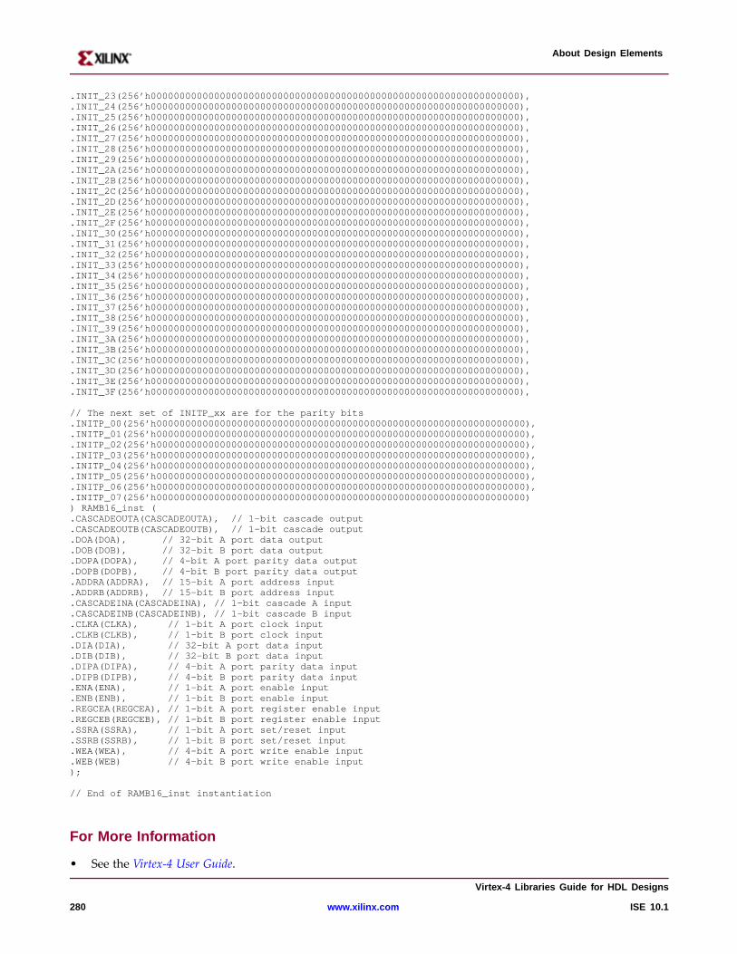
About Design Elements
.INIT_23(256’h0000000000000000000000000000000000000000000000000000000000000000),
.INIT_24(256’h0000000000000000000000000000000000000000000000000000000000000000),
.INIT_25(256’h0000000000000000000000000000000000000000000000000000000000000000),
.INIT_26(256’h0000000000000000000000000000000000000000000000000000000000000000),
.INIT_27(256’h0000000000000000000000000000000000000000000000000000000000000000),
.INIT_28(256’h0000000000000000000000000000000000000000000000000000000000000000),
.INIT_29(256’h0000000000000000000000000000000000000000000000000000000000000000),
.INIT_2A(256’h0000000000000000000000000000000000000000000000000000000000000000),
.INIT_2B(256’h0000000000000000000000000000000000000000000000000000000000000000),
.INIT_2C(256’h0000000000000000000000000000000000000000000000000000000000000000),
.INIT_2D(256’h0000000000000000000000000000000000000000000000000000000000000000),
.INIT_2E(256’h0000000000000000000000000000000000000000000000000000000000000000),
.INIT_2F(256’h0000000000000000000000000000000000000000000000000000000000000000),
.INIT_30(256’h0000000000000000000000000000000000000000000000000000000000000000),
.INIT_31(256’h0000000000000000000000000000000000000000000000000000000000000000),
.INIT_32(256’h0000000000000000000000000000000000000000000000000000000000000000),
.INIT_33(256’h0000000000000000000000000000000000000000000000000000000000000000),
.INIT_34(256’h0000000000000000000000000000000000000000000000000000000000000000),
.INIT_35(256’h0000000000000000000000000000000000000000000000000000000000000000),
.INIT_36(256’h0000000000000000000000000000000000000000000000000000000000000000),
.INIT_37(256’h0000000000000000000000000000000000000000000000000000000000000000),
.INIT_38(256’h0000000000000000000000000000000000000000000000000000000000000000),
.INIT_39(256’h0000000000000000000000000000000000000000000000000000000000000000),
.INIT_3A(256’h0000000000000000000000000000000000000000000000000000000000000000),
.INIT_3B(256’h0000000000000000000000000000000000000000000000000000000000000000),
.INIT_3C(256’h0000000000000000000000000000000000000000000000000000000000000000),
.INIT_3D(256’h0000000000000000000000000000000000000000000000000000000000000000),
.INIT_3E(256’h0000000000000000000000000000000000000000000000000000000000000000),
.INIT_3F(256’h0000000000000000000000000000000000000000000000000000000000000000),
// The next set of INITP_xx are for the parity bits.INITP_00(256’h0000000000000000000000000000000000000000000000000000000000000000),.INITP_01(256’h0000000000000000000000000000000000000000000000000000000000000000),.INITP_02(256’h0000000000000000000000000000000000000000000000000000000000000000),.INITP_03(256’h0000000000000000000000000000000000000000000000000000000000000000),.INITP_04(256’h0000000000000000000000000000000000000000000000000000000000000000),.INITP_05(256’h0000000000000000000000000000000000000000000000000000000000000000),.INITP_06(256’h0000000000000000000000000000000000000000000000000000000000000000),.INITP_07(256’h0000000000000000000000000000000000000000000000000000000000000000)) RAMB16_inst (.CASCADEOUTA(CASCADEOUTA), // 1-bit cascade output.CASCADEOUTB(CASCADEOUTB), // 1-bit cascade output.DOA(DOA), // 32-bit A port data output.DOB(DOB), // 32-bit B port data output.DOPA(DOPA), // 4-bit A port parity data output.DOPB(DOPB), // 4-bit B port parity data output.ADDRA(ADDRA), // 15-bit A port address input.ADDRB(ADDRB), // 15-bit B port address input.CASCADEINA(CASCADEINA), // 1-bit cascade A input.CASCADEINB(CASCADEINB), // 1-bit cascade B input.CLKA(CLKA), // 1-bit A port clock input.CLKB(CLKB), // 1-bit B port clock input.DIA(DIA), // 32-bit A port data input.DIB(DIB), // 32-bit B port data input.DIPA(DIPA), // 4-bit A port parity data input.DIPB(DIPB), // 4-bit B port parity data input.ENA(ENA), // 1-bit A port enable input.ENB(ENB), // 1-bit B port enable input.REGCEA(REGCEA), // 1-bit A port register enable input.REGCEB(REGCEB), // 1-bit B port register enable input.SSRA(SSRA), // 1-bit A port set/reset input.SSRB(SSRB), // 1-bit B port set/reset input.WEA(WEA), // 4-bit A port write enable input.WEB(WEB) // 4-bit B port write enable input);
// End of RAMB16_inst instantiation
For More Information
• See the Virtex-4 User Guide.
Vir tex-4 Libraries Guide for HDL Designs
280 www.xilinx.com ISE 10.1

About Design Elements
• See the Virtex-4 Data Sheets.
Vir tex-4 Libraries Guide for HDL Designs
ISE 10.1 www.xilinx.com 281
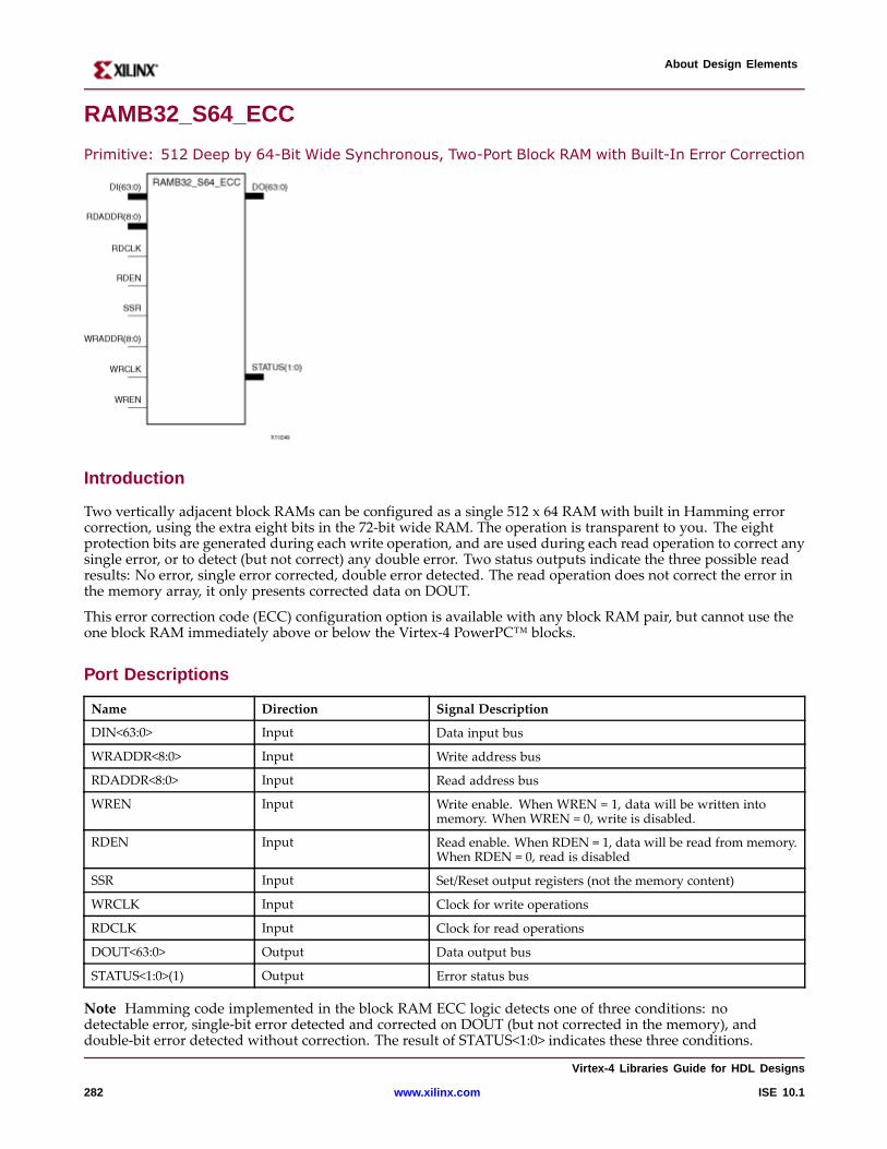
About Design Elements
RAMB32_S64_ECC
Primitive: 512 Deep by 64-Bit Wide Synchronous, Two-Port Block RAM with Built-In Error Correction
Intr oduction
Two vertically adjacent block RAMs can be configured as a single 512 x 64 RAM with built in Hamming errorcorrection, using the extra eight bits in the 72-bit wide RAM. The operation is transparent to you. The eightprotection bits are generated during each write operation, and are used during each read operation to correct anysingle error, or to detect (but not correct) any double error. Two status outputs indicate the three possible readresults: No error, single error corrected, double error detected. The read operation does not correct the error inthe memory array, it only presents corrected data on DOUT.
This error correction code (ECC) configuration option is available with any block RAM pair, but cannot use theone block RAM immediately above or below the Virtex-4 PowerPC™ blocks.
Por t Descriptions
Name Direction Signal Description
DIN<63:0> Input Data input bus
WRADDR<8:0> Input Write address bus
RDADDR<8:0> Input Read address bus
WREN Input Write enable. When WREN = 1, data will be written intomemory. When WREN = 0, write is disabled.
RDEN Input Read enable. When RDEN = 1, data will be read from memory.When RDEN = 0, read is disabled
SSR Input Set/Reset output registers (not the memory content)
WRCLK Input Clock for write operations
RDCLK Input Clock for read operations
DOUT<63:0> Output Data output bus
STATUS<1:0>(1) Output Error status bus
Note Hamming code implemented in the block RAM ECC logic detects one of three conditions: nodetectable error, single-bit error detected and corrected on DOUT (but not corrected in the memory), anddouble-bit error detected without correction. The result of STATUS<1:0> indicates these three conditions.
Vir tex-4 Libraries Guide for HDL Designs
282 www.xilinx.com ISE 10.1

About Design Elements
STATUS[1:0] Description
0 No bit error.
1 Single-bit error. The block RAM ECC macro detects and automatically corrects a single-bit error.
10 Double-bit error. The block RAM ECC macro detects a double-bit error.
11 Indeterminate state. The Hamming code implemented in the block RAM ECC cannot generate apredictable status if STATUS<1:0> is equal to three. Designers must ensure that the data has atmost double-bit errors for the STATUS<1:0> to generate the proper indicator.
Design Entr y Method
Instantiation Recommended
Inference No
Coregen and wizards No
Macro support No
Availab le Attrib utes
Attribute Type Allowed Values Default Description
DO_REG Integer 0 or 1 0 Optional output registers on A port .
SIM_COLLISION_CHECK
String “ALL”, "NONE","WARNING_ ONLY" or"GENERATE_X_ONLY”_
"ALL” Collision check enable for the allowedvalue.
VHDL Instantiation Template
Unless they already exist, copy the following two statements and paste them before the entity declaration.Library UNISIM;use UNISIM.vcomponents.all;
-- RAMB32_S64_ECC: Virtex-4 512 x 64 Error Correction BlockRAM-- Xilinx HDL Libraries Guide, version 10.1.2
RAMB32_S64_ECC_inst: RAMB32_S64_ECC_instgeneric map(DO_REG=> 0, -- Optional output registers (0 or 1)SIM_COLLISION_CHECK => "ALL") -- Collision check enable "ALL", "WARNING_ONLY", "GENERATE_X_ONLY"port map (DO => DO, -- 64-bit output dataSTATUS => STATUS, -- 2-bit status outputDI => DI, -- 64-bit data inputRDADDR=> RDADDR, -- 9-bit data address inputRDCLK => RDCLK, -- 1-bit read clock inputRDEN=> RDEN, -- 1-bit read enable inputSSR => ’0’, -- Always tie to groundWRADDR=>WRADDR, -- 9-bit write address inputWRCLK=> WRCLK, -- 1-bit write clock inputWREN=> WREN -- 1-bit write enable input);
-- End of RAMB32_S64_ECC_inst instantiation
Verilog Instantiation Template
// RAMB32_S64_ECC: Virtex-4 512 x 64 Error Correction BlockRAM// Xilinx HDL Libraries Guide, version 10.1.2
Vir tex-4 Libraries Guide for HDL Designs
ISE 10.1 www.xilinx.com 283
About Design Elements
RAMB32_S64_ECC#(.DO_REG(0), // Optional output registers (0 or 1).SIM_COLLISION_CHECK("ALL") // Collision check enable "ALL",//"WARNING_ONLY", "GENERATE_X_ONLY") RAMB32_S64_ECC_inst (.DO(DO), // 64-bit output data.STATUS(STATUS), // 2-bit status output.DI(DI), // 64-bit data input.RDADDR(RDADDR), // 9-bit data address input.RDCLK(RDCLK), // 1-bit read clock input.RDEN(RDEN), // 1-bit read enable input.SSR(1’b0), // Always tie to ground.WRADDR(WRADDR),// 9-bit write address input.WRCLK(WRCLK), // 1-bit write clock input.WREN(WREN) // 1-bit write enable input);
// End of RAMB32_S64_ECC_inst instantiation
For More Information
• See the Virtex-4 User Guide.
• See the Virtex-4 Data Sheets.
Vir tex-4 Libraries Guide for HDL Designs
284 www.xilinx.com ISE 10.1
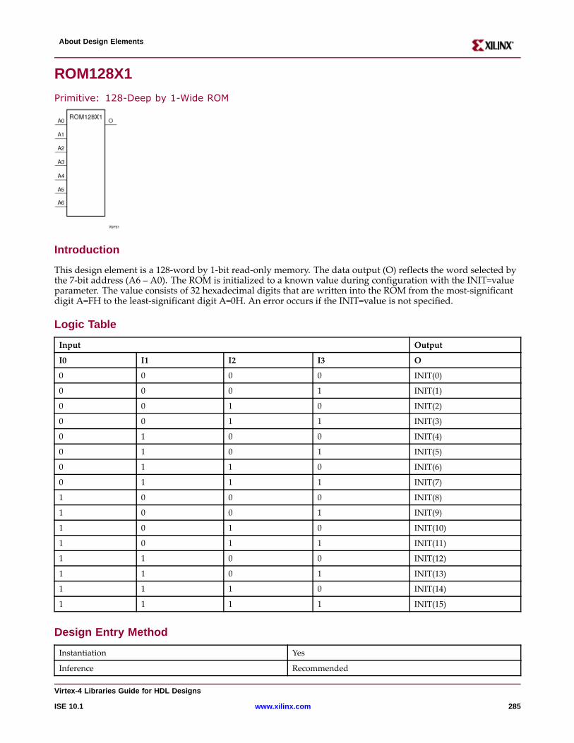
About Design Elements
ROM128X1
Primitive: 128-Deep by 1-Wide ROM
Intr oduction
This design element is a 128-word by 1-bit read-only memory. The data output (O) reflects the word selected bythe 7-bit address (A6 – A0). The ROM is initialized to a known value during configuration with the INIT=valueparameter. The value consists of 32 hexadecimal digits that are written into the ROM from the most-significantdigit A=FH to the least-significant digit A=0H. An error occurs if the INIT=value is not specified.
Logic Table
Input Output
I0 I1 I2 I3 O
0 0 0 0 INIT(0)
0 0 0 1 INIT(1)
0 0 1 0 INIT(2)
0 0 1 1 INIT(3)
0 1 0 0 INIT(4)
0 1 0 1 INIT(5)
0 1 1 0 INIT(6)
0 1 1 1 INIT(7)
1 0 0 0 INIT(8)
1 0 0 1 INIT(9)
1 0 1 0 INIT(10)
1 0 1 1 INIT(11)
1 1 0 0 INIT(12)
1 1 0 1 INIT(13)
1 1 1 0 INIT(14)
1 1 1 1 INIT(15)
Design Entr y Method
Instantiation Yes
Inference Recommended
Vir tex-4 Libraries Guide for HDL Designs
ISE 10.1 www.xilinx.com 285
About Design Elements
Coregen and wizards No
Macro support No
Availab le Attrib utes
Attribute Type Allowed Values Default Description
INIT Hexadecimal Any 128-Bit Value All zeros Specifies the contents of the ROM.
VHDL Instantiation Template
Unless they already exist, copy the following two statements and paste them before the entity declaration.Library UNISIM;use UNISIM.vcomponents.all;
-- ROM128X1: 128 x 1 Asynchronous Distributed => LUT ROM-- Virtex-II/II-Pro/4/5, Spartan-3/3E/3A-- Xilinx HDL Libraries Guide, version 10.1.2
ROM128X1_inst : ROM128X1generic map (INIT => X"00000000000000000000000000000000")port map (O => O, -- ROMoutputA0 => A0, -- ROMaddress[0]A1 => A1, -- ROMaddress[1]A2 => A2, -- ROMaddress[2]A3 => A3, -- ROMaddress[3]A4 => A4, -- ROMaddress[4]A5 => A5, -- ROMaddress[5]A6 => A6 -- ROMaddress[6]);
-- End of ROM128X1_inst instantiation
Verilog Instantiation Template
// ROM128X1: 128 x 1 Asynchronous Distributed (LUT) ROM// Virtex-II/II-Pro/4/5, Spartan-3/3E/3A// Xilinx HDL Libraries Guide, version 10.1.2
ROM128X1 #(.INIT(128’h00000000000000000000000000000000) // Contents of ROM) ROM128X1_inst (.O(O), // ROMoutput.A0(A0), // ROMaddress[0].A1(A1), // ROMaddress[1].A2(A2), // ROMaddress[2].A3(A3), // ROMaddress[3].A4(A4), // ROMaddress[4].A5(A5), // ROMaddress[5].A6(A6) // ROMaddress[6]);
// End of ROM128X1_inst instantiation
For More Information
• See the Virtex-4 User Guide.• See the Virtex-4 Data Sheets.
Vir tex-4 Libraries Guide for HDL Designs
286 www.xilinx.com ISE 10.1
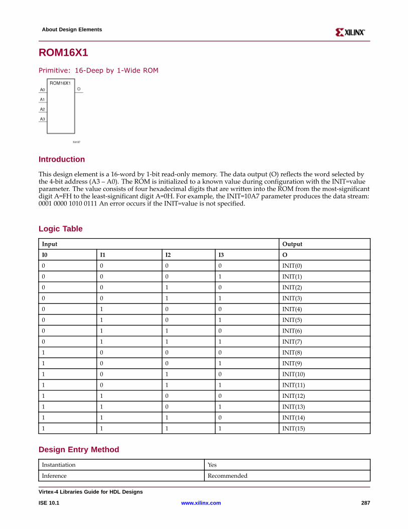
About Design Elements
ROM16X1
Primitive: 16-Deep by 1-Wide ROM
Intr oduction
This design element is a 16-word by 1-bit read-only memory. The data output (O) reflects the word selected bythe 4-bit address (A3 – A0). The ROM is initialized to a known value during configuration with the INIT=valueparameter. The value consists of four hexadecimal digits that are written into the ROM from the most-significantdigit A=FH to the least-significant digit A=0H. For example, the INIT=10A7 parameter produces the data stream:0001 0000 1010 0111 An error occurs if the INIT=value is not specified.
Logic Table
Input Output
I0 I1 I2 I3 O
0 0 0 0 INIT(0)
0 0 0 1 INIT(1)
0 0 1 0 INIT(2)
0 0 1 1 INIT(3)
0 1 0 0 INIT(4)
0 1 0 1 INIT(5)
0 1 1 0 INIT(6)
0 1 1 1 INIT(7)
1 0 0 0 INIT(8)
1 0 0 1 INIT(9)
1 0 1 0 INIT(10)
1 0 1 1 INIT(11)
1 1 0 0 INIT(12)
1 1 0 1 INIT(13)
1 1 1 0 INIT(14)
1 1 1 1 INIT(15)
Design Entr y Method
Instantiation Yes
Inference Recommended
Vir tex-4 Libraries Guide for HDL Designs
ISE 10.1 www.xilinx.com 287

About Design Elements
Coregen and wizards No
Macro support No
Availab le Attrib utes
Attribute Type Allowed Values Default Description
INIT Hexadecimal Any 16-Bit Value All zeros Specifies the contents of the ROM.
VHDL Instantiation Template
Unless they already exist, copy the following two statements and paste them before the entity declaration.Library UNISIM;use UNISIM.vcomponents.all;
-- ROM16X1: 16 x 1 Asynchronous Distributed => LUT ROM-- Xilinx HDL Libraries Guide, version 10.1.2
ROM16X1_inst : ROM16X1generic map (INIT => X"0000")port map (O => O, -- ROMoutputA0 => A0, -- ROMaddress[0]A1 => A1, -- ROMaddress[1]A2 => A2, -- ROMaddress[2]A3 => A3 -- ROMaddress[3]);
-- End of ROM16X1_inst instantiation
Verilog Instantiation Template
// ROM16X1: 16 x 1 Asynchronous Distributed (LUT) ROM// All FPGAs// Xilinx HDL Libraries Guide, version 10.1.2
ROM16X1#(.INIT(16’h0000) // Contents of ROM) ROM16X1_inst (.O(O), // ROMoutput.A0(A0), // ROMaddress[0].A1(A1), // ROMaddress[1].A2(A2), // ROMaddress[2].A3(A3) // ROMaddress[3]);
// End of ROM16X1_inst instantiation
For More Information
• See the Virtex-4 User Guide.
• See the Virtex-4 Data Sheets.
Vir tex-4 Libraries Guide for HDL Designs
288 www.xilinx.com ISE 10.1
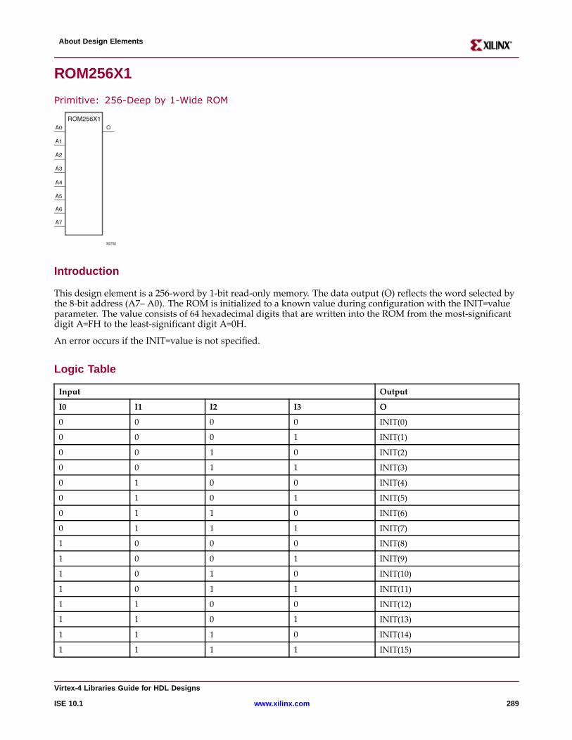
About Design Elements
ROM256X1
Primitive: 256-Deep by 1-Wide ROM
Intr oduction
This design element is a 256-word by 1-bit read-only memory. The data output (O) reflects the word selected bythe 8-bit address (A7– A0). The ROM is initialized to a known value during configuration with the INIT=valueparameter. The value consists of 64 hexadecimal digits that are written into the ROM from the most-significantdigit A=FH to the least-significant digit A=0H.
An error occurs if the INIT=value is not specified.
Logic Table
Input Output
I0 I1 I2 I3 O
0 0 0 0 INIT(0)
0 0 0 1 INIT(1)
0 0 1 0 INIT(2)
0 0 1 1 INIT(3)
0 1 0 0 INIT(4)
0 1 0 1 INIT(5)
0 1 1 0 INIT(6)
0 1 1 1 INIT(7)
1 0 0 0 INIT(8)
1 0 0 1 INIT(9)
1 0 1 0 INIT(10)
1 0 1 1 INIT(11)
1 1 0 0 INIT(12)
1 1 0 1 INIT(13)
1 1 1 0 INIT(14)
1 1 1 1 INIT(15)
Vir tex-4 Libraries Guide for HDL Designs
ISE 10.1 www.xilinx.com 289
About Design Elements
Design Entr y Method
Instantiation Yes
Inference Recommended
Coregen and wizards No
Macro support No
Availab le Attrib utes
Attribute Type Allowed Values Default Description
INIT Hexadecimal Any 256-Bit Value All zeros Specifies the contents of the ROM.
VHDL Instantiation Template
Unless they already exist, copy the following two statements and paste them before the entity declaration.Library UNISIM;use UNISIM.vcomponents.all;
-- ROM256X1: 256 x 1 Asynchronous Distributed => LUT ROM-- Virtex-II/II-Pro/4/5, Spartan-3/3E/3A-- Xilinx HDL Libraries Guide, version 10.1.2
ROM256X1_inst : ROM256X1generic map (INIT => X"0000000000000000000000000000000000000000000000000000000000000000")port map (O => O, -- ROMoutputA0 => A0, -- ROMaddress[0]A1 => A1, -- ROMaddress[1]A2 => A2, -- ROMaddress[2]A3 => A3, -- ROMaddress[3]A4 => A4, -- ROMaddress[4]A5 => A5, -- ROMaddress[5]A6 => A6, -- ROMaddress[6]A7 => A7 -- ROMaddress[7]);
-- End of ROM256X1_inst instantiation
Verilog Instantiation Template
// ROM256X1: 256 x 1 Asynchronous Distributed (LUT) ROM// Virtex-II/II-Pro/4/5, Spartan-3/3E/3A// Xilinx HDL Libraries Guide, version 10.1.2
ROM256X1 #(.INIT(256’h0000000000000000000000000000000000000000000000000000000000000000) // Contents of ROM) ROM256X1_inst (.O(O), // ROMoutput.A0(A0), // ROMaddress[0].A1(A1), // ROMaddress[1].A2(A2), // ROMaddress[2].A3(A3), // ROMaddress[3].A4(A4), // ROMaddress[4].A5(A5), // ROMaddress[5].A6(A6), // ROMaddress[6].A7(A7) // ROMaddress[7]);
// End of ROM256X1_inst instantiation
Vir tex-4 Libraries Guide for HDL Designs
290 www.xilinx.com ISE 10.1

About Design Elements
For More Information
• See the Virtex-4 User Guide.
• See the Virtex-4 Data Sheets.
Vir tex-4 Libraries Guide for HDL Designs
ISE 10.1 www.xilinx.com 291
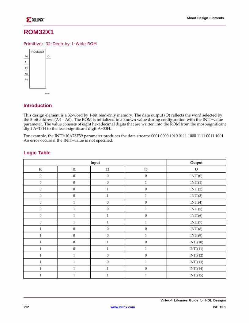
About Design Elements
ROM32X1
Primitive: 32-Deep by 1-Wide ROM
Intr oduction
This design element is a 32-word by 1-bit read-only memory. The data output (O) reflects the word selected bythe 5-bit address (A4 – A0). The ROM is initialized to a known value during configuration with the INIT=valueparameter. The value consists of eight hexadecimal digits that are written into the ROM from the most-significantdigit A=1FH to the least-significant digit A=00H.
For example, the INIT=10A78F39 parameter produces the data stream: 0001 0000 1010 0111 1000 1111 0011 1001An error occurs if the INIT=value is not specified.
Logic Table
Input Output
I0 I1 I2 I3 O
0 0 0 0 INIT(0)
0 0 0 1 INIT(1)
0 0 1 0 INIT(2)
0 0 1 1 INIT(3)
0 1 0 0 INIT(4)
0 1 0 1 INIT(5)
0 1 1 0 INIT(6)
0 1 1 1 INIT(7)
1 0 0 0 INIT(8)
1 0 0 1 INIT(9)
1 0 1 0 INIT(10)
1 0 1 1 INIT(11)
1 1 0 0 INIT(12)
1 1 0 1 INIT(13)
1 1 1 0 INIT(14)
1 1 1 1 INIT(15)
Vir tex-4 Libraries Guide for HDL Designs
292 www.xilinx.com ISE 10.1

About Design Elements
Design Entr y Method
Instantiation Yes
Inference Recommended
Coregen and wizards No
Macro support No
Availab le Attrib utes
Attribute Type Allowed Values Default Description
INIT Hexadecimal Any 32-Bit Value All zeros Specifies the contents of the ROM.
VHDL Instantiation Template
Unless they already exist, copy the following two statements and paste them before the entity declaration.Library UNISIM;use UNISIM.vcomponents.all;
-- ROM32X1: 32 x 1 Asynchronous Distributed => LUT ROM-- Xilinx HDL Libraries Guide, version 10.1.2
ROM32X1_inst : ROM32X1generic map (INIT => X"00000000")port map (O => O, -- ROMoutputA0 => A0, -- ROMaddress[0]A1 => A1, -- ROMaddress[1]A2 => A2, -- ROMaddress[2]A3 => A3, -- ROMaddress[3]A4 => A4 -- ROMaddress[4]);-- End of ROM32X1_inst instantiation
Verilog Instantiation Template
// ROM32X1: 32 x 1 Asynchronous Distributed (LUT) ROM// All FPGAs// Xilinx HDL Libraries Guide, version 10.1.2
ROM32X1#(.INIT(32’h00000000) // Contents of ROM) ROM32X1_inst (.O(O), // ROMoutput.A0(A0), // ROMaddress[0].A1(A1), // ROMaddress[1].A2(A2), // ROMaddress[2].A3(A3), // ROMaddress[3].A4(A4) // ROMaddress[4]);
// End of ROM32X1_inst instantiation
For More Information
• See the Virtex-4 User Guide.• See the Virtex-4 Data Sheets.
Vir tex-4 Libraries Guide for HDL Designs
ISE 10.1 www.xilinx.com 293

About Design Elements
ROM64X1
Primitive: 64-Deep by 1-Wide ROM
Intr oduction
This design element is a 64-word by 1-bit read-only memory. The data output (O) reflects the word selected bythe 6-bit address (A5 – A0). The ROM is initialized to a known value during configuration with the INIT=valueparameter. The value consists of 16 hexadecimal digits that are written into the ROM from the most-significantdigit A=FH to the least-significant digit A=0H. An error occurs if the INIT=value is not specified.
Logic Table
Input Output
I0 I1 I2 I3 O
0 0 0 0 INIT(0)
0 0 0 1 INIT(1)
0 0 1 0 INIT(2)
0 0 1 1 INIT(3)
0 1 0 0 INIT(4)
0 1 0 1 INIT(5)
0 1 1 0 INIT(6)
0 1 1 1 INIT(7)
1 0 0 0 INIT(8)
1 0 0 1 INIT(9)
1 0 1 0 INIT(10)
1 0 1 1 INIT(11)
1 1 0 0 INIT(12)
1 1 0 1 INIT(13)
1 1 1 0 INIT(14)
1 1 1 1 INIT(15)
Design Entr y Method
Instantiation Yes
Inference Recommended
Vir tex-4 Libraries Guide for HDL Designs
294 www.xilinx.com ISE 10.1
About Design Elements
Coregen and wizards No
Macro support No
Availab le Attrib utes
Attribute Type Allowed Values Default Description
INIT Hexadecimal Any 64-Bit Value All zeros Specifies the contents of the ROM.
VHDL Instantiation Template
Unless they already exist, copy the following two statements and paste them before the entity declaration.Library UNISIM;use UNISIM.vcomponents.all;
-- ROM64X1: 64 x 1 Asynchronous Distributed => LUT ROM-- Virtex-II/II-Pro/4/5, Spartan-3/3E/3A-- Xilinx HDL Libraries Guide, version 10.1.2
ROM64X1_inst : ROM64X1generic map (INIT => X"0000000000000000")port map (O => O, -- ROMoutputA0 => A0, -- ROMaddress[0]A1 => A1, -- ROMaddress[1]A2 => A2, -- ROMaddress[2]A3 => A3, -- ROMaddress[3]A4 => A4, -- ROMaddress[4]A5 => A5 -- ROMaddress[5]);
-- End of ROM64X1_inst instantiation
Verilog Instantiation Template
// ROM64X1: 64 x 1 Asynchronous Distributed (LUT) ROM// Virtex-II/II-Pro/4/5, Spartan-3/3E/3A// Xilinx HDL Libraries Guide, version 10.1.2
ROM64X1#(.INIT(64’h0000000000000000) // Contents of ROM) ROM64X1_inst (.O(O), // ROMoutput.A0(A0), // ROMaddress[0].A1(A1), // ROMaddress[1].A2(A2), // ROMaddress[2].A3(A3), // ROMaddress[3].A4(A4), // ROMaddress[4].A5(A5) // ROMaddress[5]);
// End of ROM64X1_inst instantiation
For More Information
• See the Virtex-4 User Guide.• See the Virtex-4 Data Sheets.
Vir tex-4 Libraries Guide for HDL Designs
ISE 10.1 www.xilinx.com 295
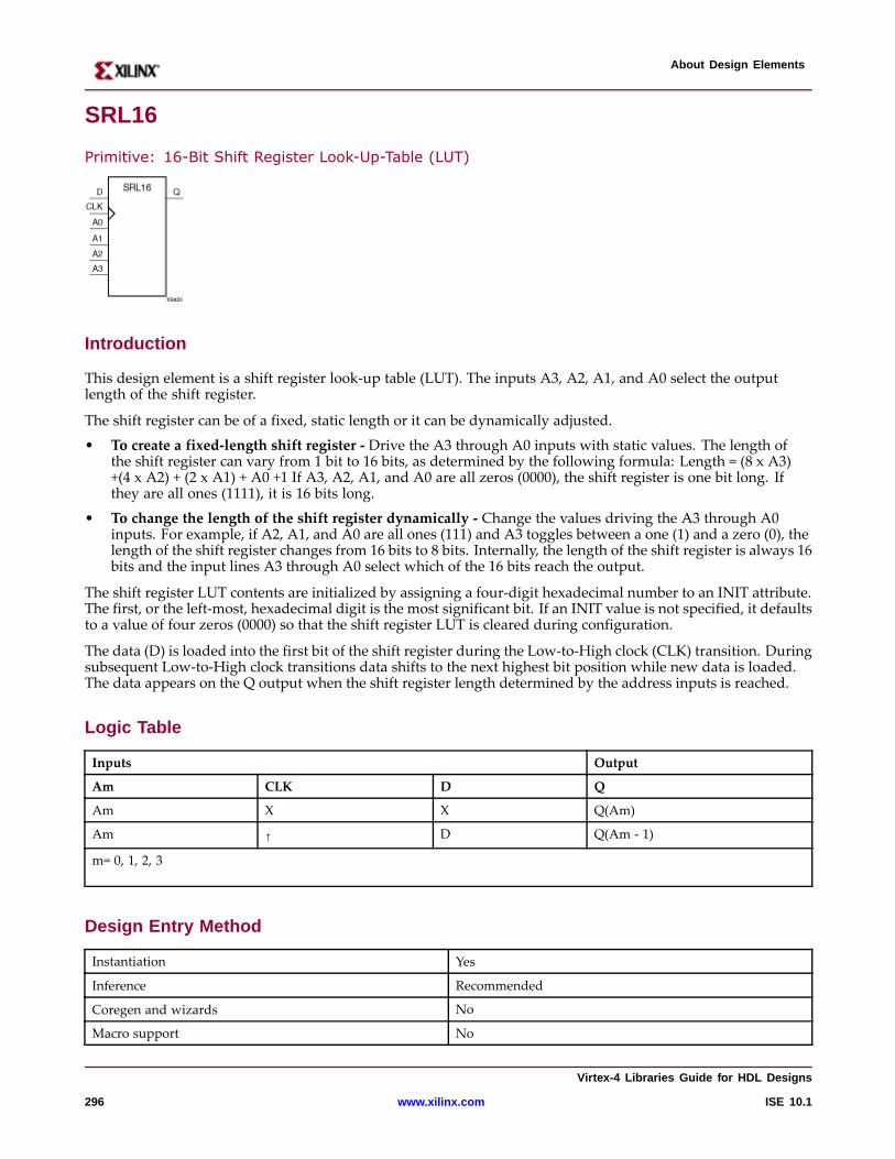
About Design Elements
SRL16
Primitive: 16-Bit Shift Register Look-Up-Table (LUT)
Intr oduction
This design element is a shift register look-up table (LUT). The inputs A3, A2, A1, and A0 select the outputlength of the shift register.
The shift register can be of a fixed, static length or it can be dynamically adjusted.
• To create a fixed-length shift register - Drive the A3 through A0 inputs with static values. The length ofthe shift register can vary from 1 bit to 16 bits, as determined by the following formula: Length = (8 x A3)+(4 x A2) + (2 x A1) + A0 +1 If A3, A2, A1, and A0 are all zeros (0000), the shift register is one bit long. Ifthey are all ones (1111), it is 16 bits long.
• To change the length of the shift register dynamically - Change the values driving the A3 through A0inputs. For example, if A2, A1, and A0 are all ones (111) and A3 toggles between a one (1) and a zero (0), thelength of the shift register changes from 16 bits to 8 bits. Internally, the length of the shift register is always 16bits and the input lines A3 through A0 select which of the 16 bits reach the output.
The shift register LUT contents are initialized by assigning a four-digit hexadecimal number to an INIT attribute.The first, or the left-most, hexadecimal digit is the most significant bit. If an INIT value is not specified, it defaultsto a value of four zeros (0000) so that the shift register LUT is cleared during configuration.
The data (D) is loaded into the first bit of the shift register during the Low-to-High clock (CLK) transition. Duringsubsequent Low-to-High clock transitions data shifts to the next highest bit position while new data is loaded.The data appears on the Q output when the shift register length determined by the address inputs is reached.
Logic Table
Inputs Output
Am CLK D Q
Am X X Q(Am)
Am ↑ D Q(Am - 1)
m= 0, 1, 2, 3
Design Entr y Method
Instantiation Yes
Inference Recommended
Coregen and wizards No
Macro support No
Vir tex-4 Libraries Guide for HDL Designs
296 www.xilinx.com ISE 10.1
About Design Elements
Availab le Attrib utes
Attribute Type Allowed Values Default Description
INIT Hexadecimal Any 16-Bit Value All zeros Sets the initial value of Q output afterconfiguration.
VHDL Instantiation Template
Unless they already exist, copy the following two statements and paste them before the entity declaration.Library UNISIM;use UNISIM.vcomponents.all;
-- SRL16: 16-bit shift register LUT operating on posedge of clock-- All FPGAs-- Xilinx HDL Libraries Guide, version 10.1.2
SRL16_inst : SRL16generic map (INIT => X"0000")port map (Q => Q, -- SRL data outputA0 => A0, -- Select[0] inputA1 => A1, -- Select[1] inputA2 => A2, -- Select[2] inputA3 => A3, -- Select[3] inputCLK => CLK, -- Clock inputD => D -- SRL data input);
-- End of SRL16_inst instantiation
Verilog Instantiation Template
// SRL16: 16-bit shift register LUT operating on posedge of clock// All FPGAs// Xilinx HDL Libraries Guide, version 10.1.2
SRL16 #(.INIT(16’h0000) // Initial Value of Shift Register) SRL16_inst (.Q(Q), // SRL data output.A0(A0), // Select[0] input.A1(A1), // Select[1] input.A2(A2), // Select[2] input.A3(A3), // Select[3] input.CLK(CLK), // Clock input.D(D) // SRL data input);
// End of SRL16_inst instantiation
For More Information
• See the Virtex-4 User Guide.
• See the Virtex-4 Data Sheets.
Vir tex-4 Libraries Guide for HDL Designs
ISE 10.1 www.xilinx.com 297
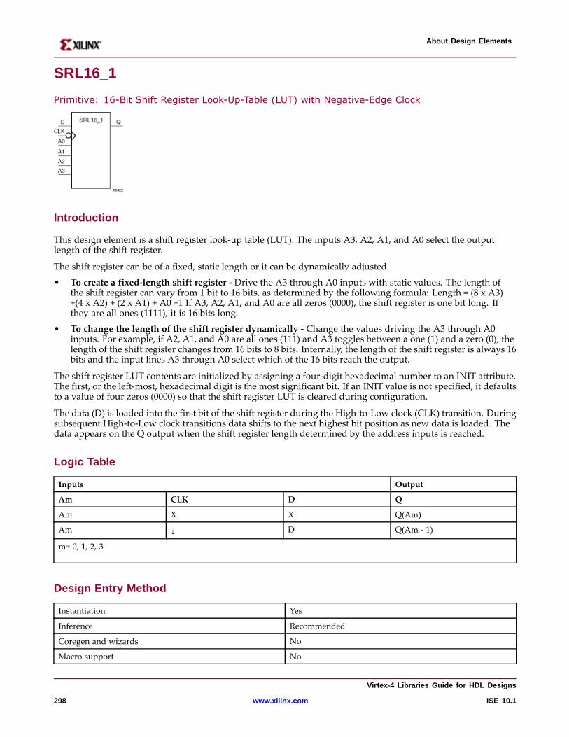
About Design Elements
SRL16_1
Primitive: 16-Bit Shift Register Look-Up-Table (LUT) with Negative-Edge Clock
Intr oduction
This design element is a shift register look-up table (LUT). The inputs A3, A2, A1, and A0 select the outputlength of the shift register.
The shift register can be of a fixed, static length or it can be dynamically adjusted.
• To create a fixed-length shift register - Drive the A3 through A0 inputs with static values. The length ofthe shift register can vary from 1 bit to 16 bits, as determined by the following formula: Length = (8 x A3)+(4 x A2) + (2 x A1) + A0 +1 If A3, A2, A1, and A0 are all zeros (0000), the shift register is one bit long. Ifthey are all ones (1111), it is 16 bits long.
• To change the length of the shift register dynamically - Change the values driving the A3 through A0inputs. For example, if A2, A1, and A0 are all ones (111) and A3 toggles between a one (1) and a zero (0), thelength of the shift register changes from 16 bits to 8 bits. Internally, the length of the shift register is always 16bits and the input lines A3 through A0 select which of the 16 bits reach the output.
The shift register LUT contents are initialized by assigning a four-digit hexadecimal number to an INIT attribute.The first, or the left-most, hexadecimal digit is the most significant bit. If an INIT value is not specified, it defaultsto a value of four zeros (0000) so that the shift register LUT is cleared during configuration.
The data (D) is loaded into the first bit of the shift register during the High-to-Low clock (CLK) transition. Duringsubsequent High-to-Low clock transitions data shifts to the next highest bit position as new data is loaded. Thedata appears on the Q output when the shift register length determined by the address inputs is reached.
Logic Table
Inputs Output
Am CLK D Q
Am X X Q(Am)
Am ↓ D Q(Am - 1)
m= 0, 1, 2, 3
Design Entr y Method
Instantiation Yes
Inference Recommended
Coregen and wizards No
Macro support No
Vir tex-4 Libraries Guide for HDL Designs
298 www.xilinx.com ISE 10.1
About Design Elements
Availab le Attrib utes
Attribute Type Allowed Values Default Description
INIT Hexadecimal Any 16-Bit Value All zeros Sets the initial value of Q output afterconfiguration
VHDL Instantiation Template
Unless they already exist, copy the following two statements and paste them before the entity declaration.Library UNISIM;use UNISIM.vcomponents.all;
-- SRL16_1: 16-bit shift register LUT operating on negedge of clock-- All FPGAs-- Xilinx HDL Libraries Guide, version 10.1.2
SRL16_1_inst : SRL16_1generic map (INIT => X"0000")port map (Q => Q, -- SRL data outputA0 => A0, -- Select[0] inputA1 => A1, -- Select[1] inputA2 => A2, -- Select[2] inputA3 => A3, -- Select[3] inputCLK => CLK, -- Clock inputD => D -- SRL data input);
-- End of SRL16_1_inst instantiation
Verilog Instantiation Template
// SRL16_1: 16-bit shift register LUT operating on negedge of clock// All FPGAs// Xilinx HDL Libraries Guide, version 10.1.2
SRL16_1 #(.INIT(16’h0000) // Initial Value of Shift Register) SRL16_1_inst (.Q(Q), // SRL data output.A0(A0), // Select[0] input.A1(A1), // Select[1] input.A2(A2), // Select[2] input.A3(A3), // Select[3] input.CLK(CLK), // Clock input.D(D) // SRL data input);
// End of SRL16_1_inst instantiation
For More Information
• See the Virtex-4 User Guide.
• See the Virtex-4 Data Sheets.
Vir tex-4 Libraries Guide for HDL Designs
ISE 10.1 www.xilinx.com 299
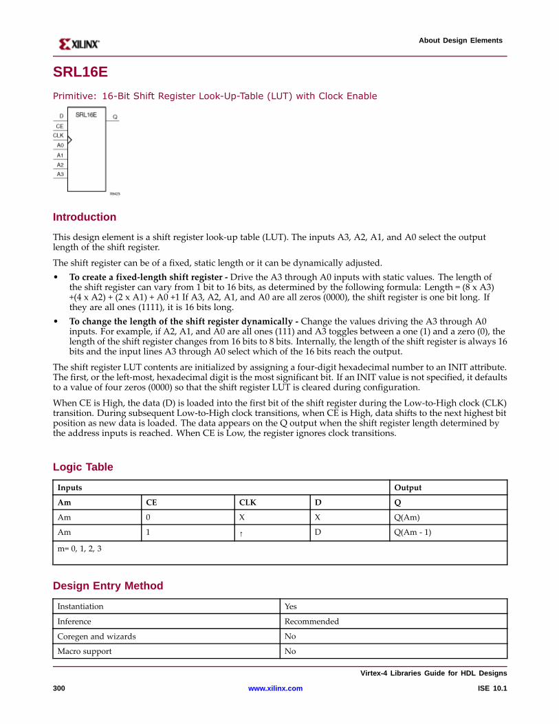
About Design Elements
SRL16E
Primitive: 16-Bit Shift Register Look-Up-Table (LUT) with Clock Enable
Intr oduction
This design element is a shift register look-up table (LUT). The inputs A3, A2, A1, and A0 select the outputlength of the shift register.
The shift register can be of a fixed, static length or it can be dynamically adjusted.• To create a fixed-length shift register - Drive the A3 through A0 inputs with static values. The length of
the shift register can vary from 1 bit to 16 bits, as determined by the following formula: Length = (8 x A3)+(4 x A2) + (2 x A1) + A0 +1 If A3, A2, A1, and A0 are all zeros (0000), the shift register is one bit long. Ifthey are all ones (1111), it is 16 bits long.
• To change the length of the shift register dynamically - Change the values driving the A3 through A0inputs. For example, if A2, A1, and A0 are all ones (111) and A3 toggles between a one (1) and a zero (0), thelength of the shift register changes from 16 bits to 8 bits. Internally, the length of the shift register is always 16bits and the input lines A3 through A0 select which of the 16 bits reach the output.
The shift register LUT contents are initialized by assigning a four-digit hexadecimal number to an INIT attribute.The first, or the left-most, hexadecimal digit is the most significant bit. If an INIT value is not specified, it defaultsto a value of four zeros (0000) so that the shift register LUT is cleared during configuration.
When CE is High, the data (D) is loaded into the first bit of the shift register during the Low-to-High clock (CLK)transition. During subsequent Low-to-High clock transitions, when CE is High, data shifts to the next highest bitposition as new data is loaded. The data appears on the Q output when the shift register length determined bythe address inputs is reached. When CE is Low, the register ignores clock transitions.
Logic Table
Inputs Output
Am CE CLK D Q
Am 0 X X Q(Am)
Am 1 ↑ D Q(Am - 1)
m= 0, 1, 2, 3
Design Entr y Method
Instantiation Yes
Inference Recommended
Coregen and wizards No
Macro support No
Vir tex-4 Libraries Guide for HDL Designs
300 www.xilinx.com ISE 10.1
About Design Elements
Availab le Attrib utes
Attribute Type Allowed Values Default Description
INIT Hexadecimal Any 16-Bit Value All zeros Sets the initial value of content and output of shiftregister after configuration.
VHDL Instantiation Template
Unless they already exist, copy the following two statements and paste them before the entity declaration.Library UNISIM;use UNISIM.vcomponents.all;
-- SRL16E: 16-bit shift register LUT with clock enable operating on posedge of clock-- All FPGAs-- Xilinx HDL Libraries Guide, version 10.1.2
SRL16E_inst : SRL16Egeneric map (INIT => X"0000")port map (Q => Q, -- SRL data outputA0 => A0, -- Select[0] inputA1 => A1, -- Select[1] inputA2 => A2, -- Select[2] inputA3 => A3, -- Select[3] inputCE => CE, -- Clock enable inputCLK => CLK, -- Clock inputD => D -- SRL data input);
-- End of SRL16E_inst instantiation
Verilog Instantiation Template
// SRL16E: 16-bit shift register LUT with clock enable operating on posedge of clock// All FPGAs// Xilinx HDL Libraries Guide, version 10.1.2
SRL16E #(.INIT(16’h0000) // Initial Value of Shift Register) SRL16E_inst (.Q(Q), // SRL data output.A0(A0), // Select[0] input.A1(A1), // Select[1] input.A2(A2), // Select[2] input.A3(A3), // Select[3] input.CE(CE), // Clock enable input.CLK(CLK), // Clock input.D(D) // SRL data input);
// End of SRL16E_inst instantiation
For More Information
• See the Virtex-4 User Guide.
• See the Virtex-4 Data Sheets.
Vir tex-4 Libraries Guide for HDL Designs
ISE 10.1 www.xilinx.com 301
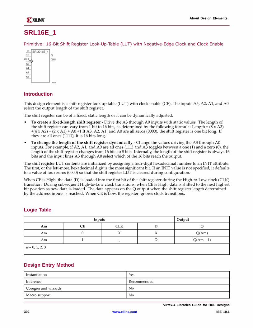
About Design Elements
SRL16E_1
Primitive: 16-Bit Shift Register Look-Up-Table (LUT) with Negative-Edge Clock and Clock Enable
Intr oduction
This design element is a shift register look up table (LUT) with clock enable (CE). The inputs A3, A2, A1, and A0select the output length of the shift register.
The shift register can be of a fixed, static length or it can be dynamically adjusted.• To create a fixed-length shift register - Drive the A3 through A0 inputs with static values. The length of
the shift register can vary from 1 bit to 16 bits, as determined by the following formula: Length = (8 x A3)+(4 x A2) + (2 x A1) + A0 +1 If A3, A2, A1, and A0 are all zeros (0000), the shift register is one bit long. Ifthey are all ones (1111), it is 16 bits long.
• To change the length of the shift register dynamically - Change the values driving the A3 through A0inputs. For example, if A2, A1, and A0 are all ones (111) and A3 toggles between a one (1) and a zero (0), thelength of the shift register changes from 16 bits to 8 bits. Internally, the length of the shift register is always 16bits and the input lines A3 through A0 select which of the 16 bits reach the output.
The shift register LUT contents are initialized by assigning a four-digit hexadecimal number to an INIT attribute.The first, or the left-most, hexadecimal digit is the most significant bit. If an INIT value is not specified, it defaultsto a value of four zeros (0000) so that the shift register LUT is cleared during configuration.
When CE is High, the data (D) is loaded into the first bit of the shift register during the High-to-Low clock (CLK)transition. During subsequent High-to-Low clock transitions, when CE is High, data is shifted to the next highestbit position as new data is loaded. The data appears on the Q output when the shift register length determinedby the address inputs is reached. When CE is Low, the register ignores clock transitions.
Logic Table
Inputs Output
Am CE CLK D Q
Am 0 X X Q(Am)
Am 1 ↓ D Q(Am - 1)
m= 0, 1, 2, 3
Design Entr y Method
Instantiation Yes
Inference Recommended
Coregen and wizards No
Macro support No
Vir tex-4 Libraries Guide for HDL Designs
302 www.xilinx.com ISE 10.1
About Design Elements
Availab le Attrib utes
Attribute Type Allowed Values Default Description
INIT Hexadecimal 16-Bit Hexadecimal All zeros Sets the initial value of content and output ofshift register after configuration.
VHDL Instantiation Template
Unless they already exist, copy the following two statements and paste them before the entity declaration.Library UNISIM;use UNISIM.vcomponents.all;
-- SRL16E_1: 16-bit shift register LUT with clock enable operating on negedge of clock-- All FPGAs-- Xilinx HDL Libraries Guide, version 10.1.2
SRL16E_1_inst : SRL16E_1generic map (INIT => X"0000")port map (Q => Q, -- SRL data outputA0 => A0, -- Select[0] inputA1 => A1, -- Select[1] inputA2 => A2, -- Select[2] inputA3 => A3, -- Select[3] inputCE => CE, -- Clock enable inputCLK => CLK, -- Clock inputD => D -- SRL data input);
-- End of SRL16E_1_inst instantiation
Verilog Instantiation Template
// SRL16E_1: 16-bit shift register LUT with clock enable operating on negedge of clock// All FPGAs// Xilinx HDL Libraries Guide, version 10.1.2
SRL16E_1 #(.INIT(16’h0000) // Initial Value of Shift Register) SRL16E_1_inst (.Q(Q), // SRL data output.A0(A0), // Select[0] input.A1(A1), // Select[1] input.A2(A2), // Select[2] input.A3(A3), // Select[3] input.CE(CE), // Clock enable input.CLK(CLK), // Clock input.D(D) // SRL data input);
// End of SRL16E_1_inst instantiation
For More Information
• See the Virtex-4 User Guide.
• See the Virtex-4 Data Sheets.
Vir tex-4 Libraries Guide for HDL Designs
ISE 10.1 www.xilinx.com 303
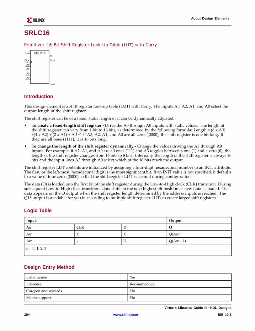
About Design Elements
SRLC16
Primitive: 16-Bit Shift Register Look-Up Table (LUT) with Carry
Intr oduction
This design element is a shift register look-up table (LUT) with Carry. The inputs A3, A2, A1, and A0 select theoutput length of the shift register.
The shift register can be of a fixed, static length or it can be dynamically adjusted.
• To create a fixed-length shift register - Drive the A3 through A0 inputs with static values. The length ofthe shift register can vary from 1 bit to 16 bits, as determined by the following formula: Length = (8 x A3)+(4 x A2) + (2 x A1) + A0 +1 If A3, A2, A1, and A0 are all zeros (0000), the shift register is one bit long. Ifthey are all ones (1111), it is 16 bits long.
• To change the length of the shift register dynamically - Change the values driving the A3 through A0inputs. For example, if A2, A1, and A0 are all ones (111) and A3 toggles between a one (1) and a zero (0), thelength of the shift register changes from 16 bits to 8 bits. Internally, the length of the shift register is always 16bits and the input lines A3 through A0 select which of the 16 bits reach the output.
The shift register LUT contents are initialized by assigning a four-digit hexadecimal number to an INIT attribute.The first, or the left-most, hexadecimal digit is the most significant bit. If an INIT value is not specified, it defaultsto a value of four zeros (0000) so that the shift register LUT is cleared during configuration.
The data (D) is loaded into the first bit of the shift register during the Low-to-High clock (CLK) transition. Duringsubsequent Low-to-High clock transitions data shifts to the next highest bit position as new data is loaded. Thedata appears on the Q output when the shift register length determined by the address inputs is reached. TheQ15 output is available for you in cascading to multiple shift register LUTs to create larger shift registers.
Logic Table
Inputs Output
Am CLK D Q
Am X X Q(Am)
Am ↑ D Q(Am - 1)
m= 0, 1, 2, 3
Design Entr y Method
Instantiation Yes
Inference Recommended
Coregen and wizards No
Macro support No
Vir tex-4 Libraries Guide for HDL Designs
304 www.xilinx.com ISE 10.1

About Design Elements
Availab le Attrib utes
Attribute Type Allowed Values Default Description
INIT Hexadecimal Any 16-Bit Valuel All zeros Sets the initial value of content and output of shiftregister after configuration.
VHDL Instantiation Template
Unless they already exist, copy the following two statements and paste them before the entity declaration.Library UNISIM;use UNISIM.vcomponents.all;
-- SRLC16: 16-bit cascadable shift register LUT operating on posedge of clock-- Virtex-II/II-Pro, Spartan-3/3E/3A-- Xilinx HDL Libraries Guide, version 10.1.2
SRLC16_inst : SRLC16generic map (INIT => X"0000")port map (Q => Q, -- SRL data outputQ15 => Q15, -- Carry output (connect to next SRL)A0 => A0, -- Select[0] inputA1 => A1, -- Select[1] inputA2 => A2, -- Select[2] inputA3 => A3, -- Select[3] inputCLK => CLK, -- Clock inputD => D -- SRL data input);
-- End of SRLC16_inst instantiation
Verilog Instantiation Template
// SRLC16: 16-bit cascadable shift register LUT operating on posedge of clock// Virtex-II/II-Pro/4, Spartan-3/3E/3A// Xilinx HDL Libraries Guide, version 10.1.2
SRLC16 #(.INIT(16’h0000) // Initial Value of Shift Register) SRLC16_inst (.Q(Q), // SRL data output.Q15(Q15), // Carry output (connect to next SRL).A0(A0), // Select[0] input.A1(A1), // Select[1] input.A2(A2), // Select[2] input.A3(A3), // Select[3] input.CLK(CLK), // Clock input.D(D) // SRL data input);
// End of SRLC16_inst instantiation
For More Information
• See the Virtex-4 User Guide.
• See the Virtex-4 Data Sheets.
Vir tex-4 Libraries Guide for HDL Designs
ISE 10.1 www.xilinx.com 305
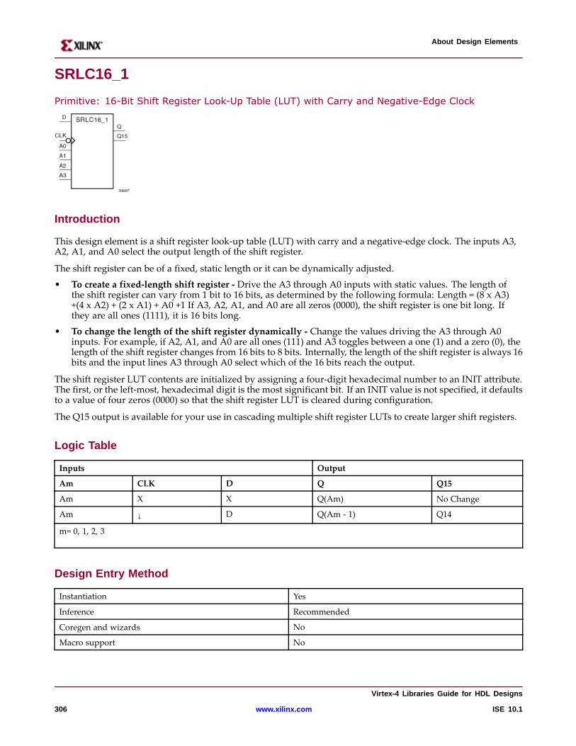
About Design Elements
SRLC16_1
Primitive: 16-Bit Shift Register Look-Up Table (LUT) with Carry and Negative-Edge Clock
Intr oduction
This design element is a shift register look-up table (LUT) with carry and a negative-edge clock. The inputs A3,A2, A1, and A0 select the output length of the shift register.
The shift register can be of a fixed, static length or it can be dynamically adjusted.
• To create a fixed-length shift register - Drive the A3 through A0 inputs with static values. The length ofthe shift register can vary from 1 bit to 16 bits, as determined by the following formula: Length = (8 x A3)+(4 x A2) + (2 x A1) + A0 +1 If A3, A2, A1, and A0 are all zeros (0000), the shift register is one bit long. Ifthey are all ones (1111), it is 16 bits long.
• To change the length of the shift register dynamically - Change the values driving the A3 through A0inputs. For example, if A2, A1, and A0 are all ones (111) and A3 toggles between a one (1) and a zero (0), thelength of the shift register changes from 16 bits to 8 bits. Internally, the length of the shift register is always 16bits and the input lines A3 through A0 select which of the 16 bits reach the output.
The shift register LUT contents are initialized by assigning a four-digit hexadecimal number to an INIT attribute.The first, or the left-most, hexadecimal digit is the most significant bit. If an INIT value is not specified, it defaultsto a value of four zeros (0000) so that the shift register LUT is cleared during configuration.
The Q15 output is available for your use in cascading multiple shift register LUTs to create larger shift registers.
Logic Table
Inputs Output
Am CLK D Q Q15
Am X X Q(Am) No Change
Am ↓ D Q(Am - 1) Q14
m= 0, 1, 2, 3
Design Entr y Method
Instantiation Yes
Inference Recommended
Coregen and wizards No
Macro support No
Vir tex-4 Libraries Guide for HDL Designs
306 www.xilinx.com ISE 10.1
About Design Elements
Availab le Attrib utes
Attribute Type Allowed Values Default Description
INIT Hexadecimal Any 16-Bit Value All zeros Sets the initial value of content and output of shiftregister after configuration.
VHDL Instantiation Template
Unless they already exist, copy the following two statements and paste them before the entity declaration.Library UNISIM;use UNISIM.vcomponents.all;
-- SRLC16_1: 16-bit cascadable shift register LUT operating on negedge of clock-- Virtex-II/II-Pro, Spartan-3/3E/3A-- Xilinx HDL Libraries Guide, version 10.1.2
SRLC16_1_inst : SRLC16_1generic map (INIT => X"0000")port map (Q => Q, -- SRL data outputQ15 => Q15, -- Carry output (connect to next SRL)A0 => A0, -- Select[0] inputA1 => A1, -- Select[1] inputA2 => A2, -- Select[2] inputA3 => A3, -- Select[3] inputCLK => CLK, -- Clock inputD => D -- SRL data input);
-- End of SRLC16_1_inst instantiation
Verilog Instantiation Template
// SRLC16_1: 16-bit cascadable shift register LUT operating on negedge of clock// Virtex-II/II-Pro/4, Spartan-3/3E/3A// Xilinx HDL Libraries Guide, version 10.1.2
SRLC16_1 #(.INIT(16’h0000) // Initial Value of Shift Register) SRLC16_1_inst (.Q(Q), // SRL data output.Q15(Q15), // Carry output (connect to next SRL).A0(A0), // Select[0] input.A1(A1), // Select[1] input.A2(A2), // Select[2] input.A3(A3), // Select[3] input.CLK(CLK), // Clock input.D(D) // SRL data input);
// End of SRLC16_1_inst instantiation
For More Information
• See the Virtex-4 User Guide.
• See the Virtex-4 Data Sheets.
Vir tex-4 Libraries Guide for HDL Designs
ISE 10.1 www.xilinx.com 307
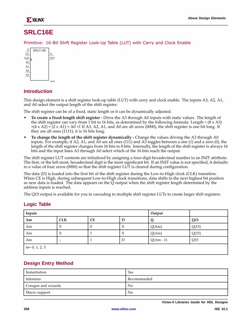
About Design Elements
SRLC16E
Primitive: 16-Bit Shift Register Look-Up Table (LUT) with Carry and Clock Enable
Intr oduction
This design element is a shift register look-up table (LUT) with carry and clock enable. The inputs A3, A2, A1,and A0 select the output length of the shift register.
The shift register can be of a fixed, static length or it can be dynamically adjusted.• To create a fixed-length shift register - Drive the A3 through A0 inputs with static values. The length of
the shift register can vary from 1 bit to 16 bits, as determined by the following formula: Length = (8 x A3)+(4 x A2) + (2 x A1) + A0 +1 If A3, A2, A1, and A0 are all zeros (0000), the shift register is one bit long. Ifthey are all ones (1111), it is 16 bits long.
• To change the length of the shift register dynamically - Change the values driving the A3 through A0inputs. For example, if A2, A1, and A0 are all ones (111) and A3 toggles between a one (1) and a zero (0), thelength of the shift register changes from 16 bits to 8 bits. Internally, the length of the shift register is always 16bits and the input lines A3 through A0 select which of the 16 bits reach the output.
The shift register LUT contents are initialized by assigning a four-digit hexadecimal number to an INIT attribute.The first, or the left-most, hexadecimal digit is the most significant bit. If an INIT value is not specified, it defaultsto a value of four zeros (0000) so that the shift register LUT is cleared during configuration.
The data (D) is loaded into the first bit of the shift register during the Low-to-High clock (CLK) transition.When CE is High, during subsequent Low-to-High clock transitions, data shifts to the next highest bit positionas new data is loaded. The data appears on the Q output when the shift register length determined by theaddress inputs is reached.
The Q15 output is available for you in cascading to multiple shift register LUTs to create larger shift registers.
Logic Table
Inputs Output
Am CLK CE D Q Q15
Am X 0 X Q(Am) Q(15)
Am X 1 X Q(Am) Q(15)
Am ↑ 1 D Q(Am - 1) Q15
m= 0, 1, 2, 3
Design Entr y Method
Instantiation Yes
Inference Recommended
Coregen and wizards No
Macro support No
Vir tex-4 Libraries Guide for HDL Designs
308 www.xilinx.com ISE 10.1
About Design Elements
Availab le Attrib utes
Attribute Type Allowed Values Default Description
INIT Hexadecimal Any 16-Bit Value All zeros Sets the initial value of content and output of shiftregister after configuration.
VHDL Instantiation Template
Unless they already exist, copy the following two statements and paste them before the entity declaration.Library UNISIM;use UNISIM.vcomponents.all;
-- SRLC16E: 16-bit cascable shift register LUT with clock enable operating on posedge of clock-- Virtex-II/II-Pro, Spartan-3/3E/3A-- Xilinx HDL Libraries Guide, version 10.1.2
SRLC16E_inst : SRLC16Egeneric map (INIT => X"0000")port map (Q => Q, -- SRL data outputQ15 => Q15, -- Carry output (connect to next SRL)A0 => A0, -- Select[0] inputA1 => A1, -- Select[1] inputA2 => A2, -- Select[2] inputA3 => A3, -- Select[3] inputCE => CE, -- Clock enable inputCLK => CLK, -- Clock inputD => D -- SRL data input);
-- End of SRLC16E_inst instantiation
Verilog Instantiation Template
// SRLC16E: 16-bit cascadable shift register LUT with clock enable operating on posedge of clock// Virtex-II/II-Pro/4, Spartan-3/3E/3A// Xilinx HDL Libraries Guide, version 10.1.2
SRLC16E #(.INIT(16’h0000) // Initial Value of Shift Register) SRLC16E_inst (.Q(Q), // SRL data output.Q15(Q15), // Carry output (connect to next SRL).A0(A0), // Select[0] input.A1(A1), // Select[1] input.A2(A2), // Select[2] input.A3(A3), // Select[3] input.CE(CE), // Clock enable input.CLK(CLK), // Clock input.D(D) // SRL data input);
// End of SRLC16E_inst instantiation
For More Information
• See the Virtex-4 User Guide.
• See the Virtex-4 Data Sheets.
Vir tex-4 Libraries Guide for HDL Designs
ISE 10.1 www.xilinx.com 309
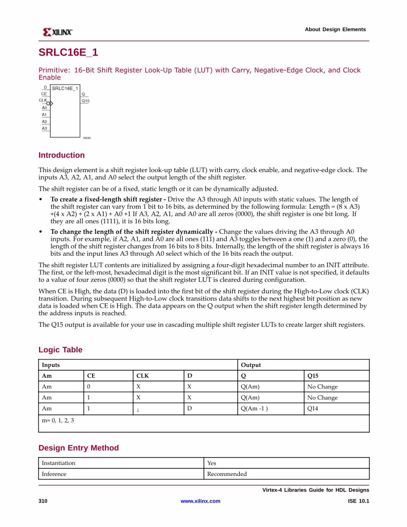
About Design Elements
SRLC16E_1
Primitive: 16-Bit Shift Register Look-Up Table (LUT) with Carry, Negative-Edge Clock, and ClockEnable
Intr oduction
This design element is a shift register look-up table (LUT) with carry, clock enable, and negative-edge clock. Theinputs A3, A2, A1, and A0 select the output length of the shift register.
The shift register can be of a fixed, static length or it can be dynamically adjusted.• To create a fixed-length shift register - Drive the A3 through A0 inputs with static values. The length of
the shift register can vary from 1 bit to 16 bits, as determined by the following formula: Length = (8 x A3)+(4 x A2) + (2 x A1) + A0 +1 If A3, A2, A1, and A0 are all zeros (0000), the shift register is one bit long. Ifthey are all ones (1111), it is 16 bits long.
• To change the length of the shift register dynamically - Change the values driving the A3 through A0inputs. For example, if A2, A1, and A0 are all ones (111) and A3 toggles between a one (1) and a zero (0), thelength of the shift register changes from 16 bits to 8 bits. Internally, the length of the shift register is always 16bits and the input lines A3 through A0 select which of the 16 bits reach the output.
The shift register LUT contents are initialized by assigning a four-digit hexadecimal number to an INIT attribute.The first, or the left-most, hexadecimal digit is the most significant bit. If an INIT value is not specified, it defaultsto a value of four zeros (0000) so that the shift register LUT is cleared during configuration.
When CE is High, the data (D) is loaded into the first bit of the shift register during the High-to-Low clock (CLK)transition. During subsequent High-to-Low clock transitions data shifts to the next highest bit position as newdata is loaded when CE is High. The data appears on the Q output when the shift register length determined bythe address inputs is reached.
The Q15 output is available for your use in cascading multiple shift register LUTs to create larger shift registers.
Logic Table
Inputs Output
Am CE CLK D Q Q15
Am 0 X X Q(Am) No Change
Am 1 X X Q(Am) No Change
Am 1 ↓ D Q(Am -1 ) Q14
m= 0, 1, 2, 3
Design Entr y Method
Instantiation Yes
Inference Recommended
Vir tex-4 Libraries Guide for HDL Designs
310 www.xilinx.com ISE 10.1
About Design Elements
Coregen and wizards No
Macro support No
Availab le Attrib utes
Attribute TypeAllowedValues Default Description
INIT Hexadecimal Any 16-BitValue
All zeros Sets the initial value of content and output of shift registerafter configuration.
VHDL Instantiation Template
Unless they already exist, copy the following two statements and paste them before the entity declaration.Library UNISIM;use UNISIM.vcomponents.all;
-- SRLC16E_1: 16-bit shift register LUT with clock enable operating on negedge of clock-- Virtex-II/II-Pro, Spartan-3/3E/3A-- Xilinx HDL Libraries Guide, version 10.1.2
SRLC16E_1_inst : SRLC16E_1generic map (INIT => X"0000")port map (Q => Q, -- SRL data outputQ15 => Q15, -- Carry output (connect to next SRL)A0 => A0, -- Select[0] inputA1 => A1, -- Select[1] inputA2 => A2, -- Select[2] inputA3 => A3, -- Select[3] inputCE => CE, -- Clock enable inputCLK => CLK, -- Clock inputD => D -- SRL data input);
-- End of SRLC16E_1_inst instantiation
Verilog Instantiation Template
// SRLC16E_1: 16-bit shift register LUT with clock enable operating on negedge of clock// Virtex-II/II-Pro/4, Spartan-3/3E/3A// Xilinx HDL Libraries Guide, version 10.1.2
SRLC16E_1 #(.INIT(16’h0000) // Initial Value of Shift Register) SRLC16E_1_inst (.Q(Q), // SRL data output.Q15(Q15), // Carry output (connect to next SRL).A0(A0), // Select[0] input.A1(A1), // Select[1] input.A2(A2), // Select[2] input.A3(A3), // Select[3] input.CE(CE), // Clock enable input.CLK(CLK), // Clock input.D(D) // SRL data input);
// End of SRLC16E_1_inst instantiation
Vir tex-4 Libraries Guide for HDL Designs
ISE 10.1 www.xilinx.com 311

About Design Elements
For More Information
• See the Virtex-4 User Guide.
• See the Virtex-4 Data Sheets.
Vir tex-4 Libraries Guide for HDL Designs
312 www.xilinx.com ISE 10.1
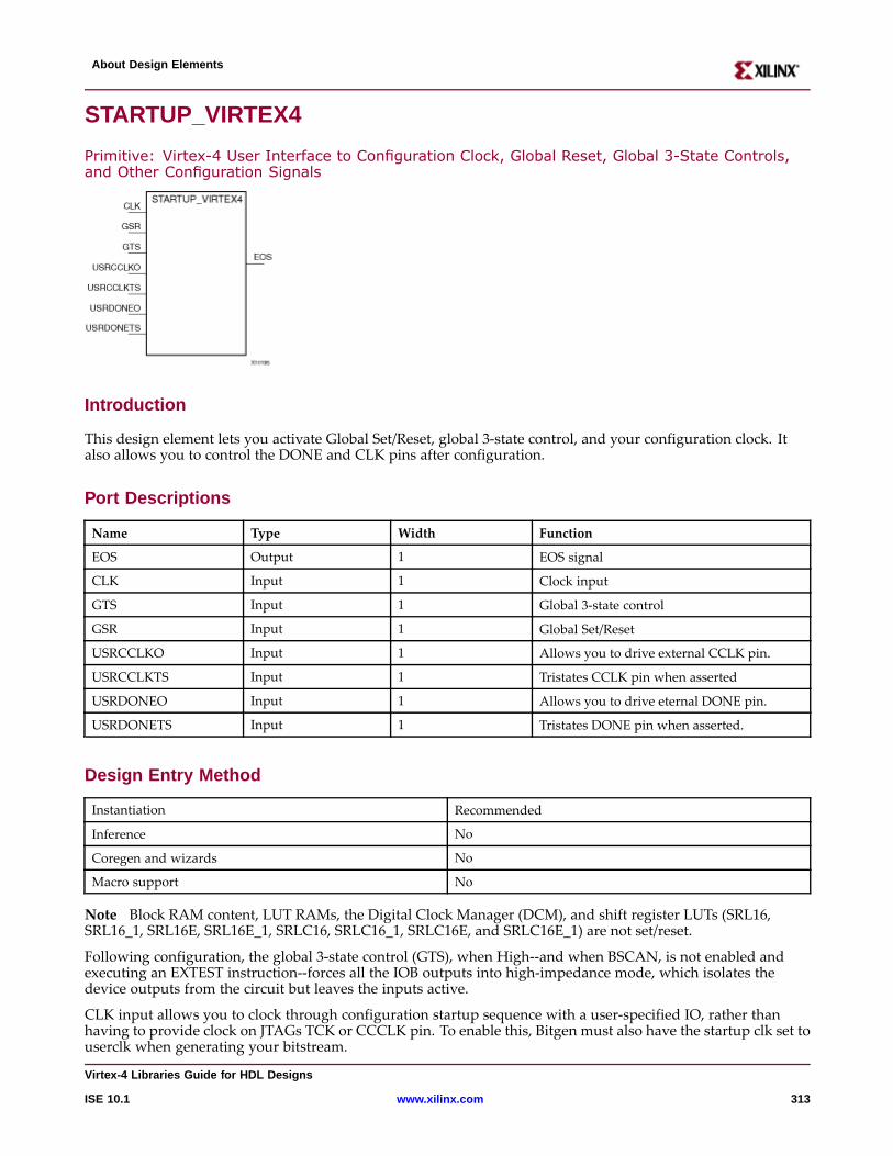
About Design Elements
STARTUP_VIRTEX4
Primitive: Virtex-4 User Interface to Configuration Clock, Global Reset, Global 3-State Controls,and Other Configuration Signals
Intr oduction
This design element lets you activate Global Set/Reset, global 3-state control, and your configuration clock. Italso allows you to control the DONE and CLK pins after configuration.
Por t Descriptions
Name Type Width Function
EOS Output 1 EOS signal
CLK Input 1 Clock input
GTS Input 1 Global 3-state control
GSR Input 1 Global Set/Reset
USRCCLKO Input 1 Allows you to drive external CCLK pin.
USRCCLKTS Input 1 Tristates CCLK pin when asserted
USRDONEO Input 1 Allows you to drive eternal DONE pin.
USRDONETS Input 1 Tristates DONE pin when asserted.
Design Entr y Method
Instantiation Recommended
Inference No
Coregen and wizards No
Macro support No
Note Block RAM content, LUT RAMs, the Digital Clock Manager (DCM), and shift register LUTs (SRL16,SRL16_1, SRL16E, SRL16E_1, SRLC16, SRLC16_1, SRLC16E, and SRLC16E_1) are not set/reset.
Following configuration, the global 3-state control (GTS), when High--and when BSCAN, is not enabled andexecuting an EXTEST instruction--forces all the IOB outputs into high-impedance mode, which isolates thedevice outputs from the circuit but leaves the inputs active.
CLK input allows you to clock through configuration startup sequence with a user-specified IO, rather thanhaving to provide clock on JTAGs TCK or CCCLK pin. To enable this, Bitgen must also have the startup clk set touserclk when generating your bitstream.
Vir tex-4 Libraries Guide for HDL Designs
ISE 10.1 www.xilinx.com 313
About Design Elements
USRCLKO/TS and USRDONEO/TS are used to control the external DONE and CCLK pins. Using theSTARTUP_VIRTEX4 in combination with the USR_ACCESS_VIRTEX4 primitive supports a variety ofapplications, such as loading PROM data into the FPGA for various uses. Refer to USR_ACCESS_VIRTEX4 formore information.
VHDL Instantiation Template
Unless they already exist, copy the following two statements and paste them before the entity declaration.Library UNISIM;use UNISIM.vcomponents.all;
-- STARTUP_VIRTEX4: Startup primitive for GSR, GTS or startup sequence-- control. Virtex-4-- Xilinx HDL Libraries Guide, version 10.1.2STARTUP_VIRTEX4_inst : STARTUP_VIRTEX4port map (EOS => EOS, -- End of Startup 1-bit outputCLK => CLK, -- Clock input for start-up sequenceGSR => GSR_PORT, -- Global Set/Reset input (GSR cannot be used for the port name)GTS => GTS_PORT, -- Global 3-state input (GTS cannot be used for the port name)USRCCLKO=> USRCCLKO, -- USRCCLKO1-bit inputUSRCCLKTS=> USRCCLKTS, -- USRCCLKTS1-bit inputUSRDONEO=> USRDONEO, -- USRDONEO1-bit inputUSRDONETS=> USRDONETS -- USRDONETS1-bit input);
-- End of STARTUP_VIRTEX4_inst instantiation
Verilog Instantiation Template
// STARTUP_VIRTEX4: Startup primitive for GSR, GTS or startup sequence// control. Virtex-4// Xilinx HDL Libraries Guide, version 10.1.2
STARTUP_VIRTEX4 STARTUP_VIRTEX4_inst (.EOS(EOS), // End Of Startup 1-bit output.CLK(CLK), // Clock input for start-up sequence.GSR(GSR_PORT), // Global Set/Reset input (GSR can not be used as a port name).GTS(GTS_PORT), // Global 3-state input (GTS can not be used as a port name).USRCCLKO(USRCCLKO), // USERCLK01-bit input.USRCCLKTS(USRCCLKTS), // USERCLKTS1-bit input.USRDONEO(USRDONEO),// USRDONE01-bit input.USRDONETS(USRDONETS)// USRDONETS1-bit input);
// End of STARTUP_VIRTEX4_inst instantiation
For More Information
• See the Virtex-4 User Guide.
• See the Virtex-4 Data Sheets.
Vir tex-4 Libraries Guide for HDL Designs
314 www.xilinx.com ISE 10.1
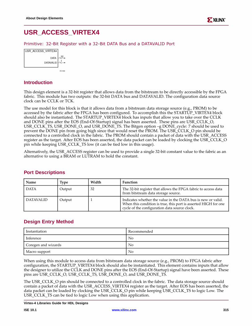
About Design Elements
USR_ACCESS_VIRTEX4
Primitive: 32-Bit Register with a 32-Bit DATA Bus and a DATAVALID Port
Intr oduction
This design element is a 32-bit register that allows data from the bitstream to be directly accessible by the FPGAfabric. This module has two outputs: the 32-bit DATA bus and DATAVALID. The configuration data sourceclock can be CCLK or TCK.
The use model for this block is that it allows data from a bitstream data storage source (e.g., PROM) to beaccessed by the fabric after the FPGA has been configured. To accomplish this the STARTUP_VIRTEX4 blockshould also be instantiated. The STARTUP_VIRTEX4 block has inputs that allow you to take over the CCLKand DONE pins after the EOS (End-Of-Startup) signal has been asserted. These pins are USR_CCLK_O,USR_CCLK_TS, USR_DONE_O, and USR_DONE_TS. The Bitgen option –g DONE_cycle: 7 should be used toprevent the DONE pin from going high since that would reset the PROM. The USR_CCLK_O pin should beconnected to a controlled clock in the fabric. The PROM should contain a packet of data with the USR_ACCESSregister as the target. After EOS has been asserted, the data packet can be loaded by clocking the USR_CCLK_Opin while keeping USR_CCLK_TS low (it can be tied low in this usage).
Alternatively, the USR_ACCESS register can be used to provide a single 32-bit constant value to the fabric as analternative to using a BRAM or LUTRAM to hold the constant.
Por t Descriptions
Name Type Width Function
DATA Output 32 The 32-bit register that allows the FPGA fabric to access datafrom bitstream data storage source.
DATAVALID Output 1 Indicates whether the value in the DATA bus is new or valid.When this condition is true, this port is asserted HIGH for onecycle of the configuration data source clock.
Design Entr y Method
Instantiation Recommended
Inference No
Coregen and wizards No
Macro support No
When using this module to access data from bitstream data storage source (e.g., PROM) to FPGA fabric afterconfiguration, the STARTUP_VIRTEX4 block should also be instantiated. This element contains inputs that allowthe designer to utilize the CCLK and DONE pins after the EOS (End-Of-Startup) signal have been asserted. Thesepins are USR_CCLK_O, USR_CCLK_TS, USR_DONE_O, and USR_DONE_TS.
The USR_CCLK_O pin should be connected to a controlled clock in the fabric. The data storage source shouldcontain a packet of data with the USR_ACCESS_VIRTEX4 register as the target. After EOS has been asserted, thedata packet can be loaded by clocking the USR_CCLK_O pin while keeping USR_CCLK_TS to logic Low. TheUSR_CCLK_TS can be tied to logic Low when using this application.
Vir tex-4 Libraries Guide for HDL Designs
ISE 10.1 www.xilinx.com 315
About Design Elements
In addition, when using this module, the bitgen option –g DONE_cycle: 7 should be used to prevent the Highassertion of DONE pin. Should the DONE pin be asserted High, the PROM will be reset.
Vir tex-4 Libraries Guide for HDL Designs
316 www.xilinx.com ISE 10.1

About Design Elements
For More Information
• See the Virtex-4 User Guide.
• See the Virtex-4 Data Sheets.
Vir tex-4 Libraries Guide for HDL Designs
ISE 10.1 www.xilinx.com 317
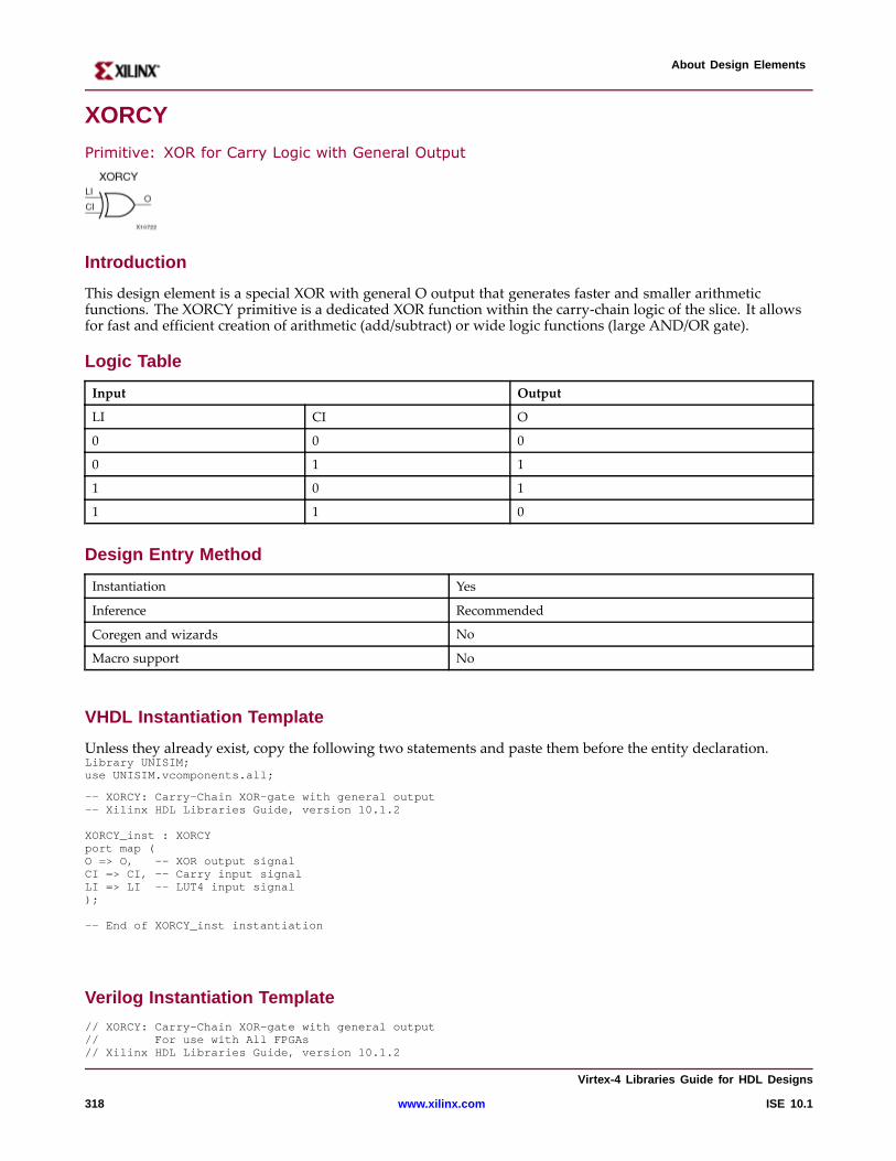
About Design Elements
XORCY
Primitive: XOR for Carry Logic with General Output
Intr oduction
This design element is a special XOR with general O output that generates faster and smaller arithmeticfunctions. The XORCY primitive is a dedicated XOR function within the carry-chain logic of the slice. It allowsfor fast and efficient creation of arithmetic (add/subtract) or wide logic functions (large AND/OR gate).
Logic Table
Input Output
LI CI O
0 0 0
0 1 1
1 0 1
1 1 0
Design Entr y Method
Instantiation Yes
Inference Recommended
Coregen and wizards No
Macro support No
VHDL Instantiation Template
Unless they already exist, copy the following two statements and paste them before the entity declaration.Library UNISIM;use UNISIM.vcomponents.all;
-- XORCY: Carry-Chain XOR-gate with general output-- Xilinx HDL Libraries Guide, version 10.1.2
XORCY_inst : XORCYport map (O => O, -- XOR output signalCI => CI, -- Carry input signalLI => LI -- LUT4 input signal);
-- End of XORCY_inst instantiation
Verilog Instantiation Template
// XORCY: Carry-Chain XOR-gate with general output// For use with All FPGAs// Xilinx HDL Libraries Guide, version 10.1.2
Vir tex-4 Libraries Guide for HDL Designs
318 www.xilinx.com ISE 10.1
About Design Elements
XORCYXORCY_inst (.O(O), // XOR output signal.CI(CI), // Carry input signal.LI(LI) // LUT4 input signal);
// End of XORCY_inst instantiation
For More Information
• See the Virtex-4 User Guide.
• See the Virtex-4 Data Sheets.
Vir tex-4 Libraries Guide for HDL Designs
ISE 10.1 www.xilinx.com 319
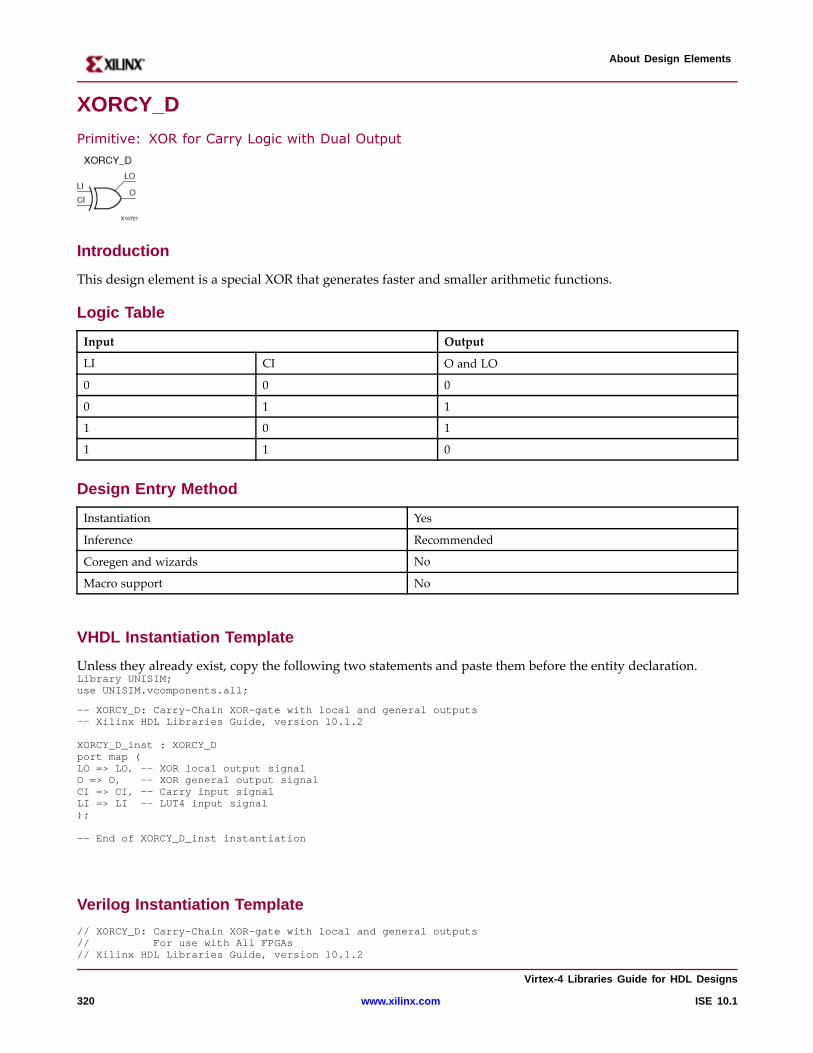
About Design Elements
XORCY_D
Primitive: XOR for Carry Logic with Dual Output
Intr oduction
This design element is a special XOR that generates faster and smaller arithmetic functions.
Logic Table
Input Output
LI CI O and LO
0 0 0
0 1 1
1 0 1
1 1 0
Design Entr y Method
Instantiation Yes
Inference Recommended
Coregen and wizards No
Macro support No
VHDL Instantiation Template
Unless they already exist, copy the following two statements and paste them before the entity declaration.Library UNISIM;use UNISIM.vcomponents.all;
-- XORCY_D: Carry-Chain XOR-gate with local and general outputs-- Xilinx HDL Libraries Guide, version 10.1.2
XORCY_D_inst : XORCY_Dport map (LO => LO, -- XOR local output signalO => O, -- XOR general output signalCI => CI, -- Carry input signalLI => LI -- LUT4 input signal);
-- End of XORCY_D_inst instantiation
Verilog Instantiation Template
// XORCY_D: Carry-Chain XOR-gate with local and general outputs// For use with All FPGAs// Xilinx HDL Libraries Guide, version 10.1.2
Vir tex-4 Libraries Guide for HDL Designs
320 www.xilinx.com ISE 10.1
About Design Elements
XORCY_DXORCY_D_inst (.LO(LO), // XOR local output signal.O(O), // XOR general output signal.CI(CI), // Carry input signal.LI(LI) // LUT4 input signal);
// End of XORCY_D_inst instantiation
For More Information
• See the Virtex-4 User Guide.
• See the Virtex-4 Data Sheets.
Vir tex-4 Libraries Guide for HDL Designs
ISE 10.1 www.xilinx.com 321
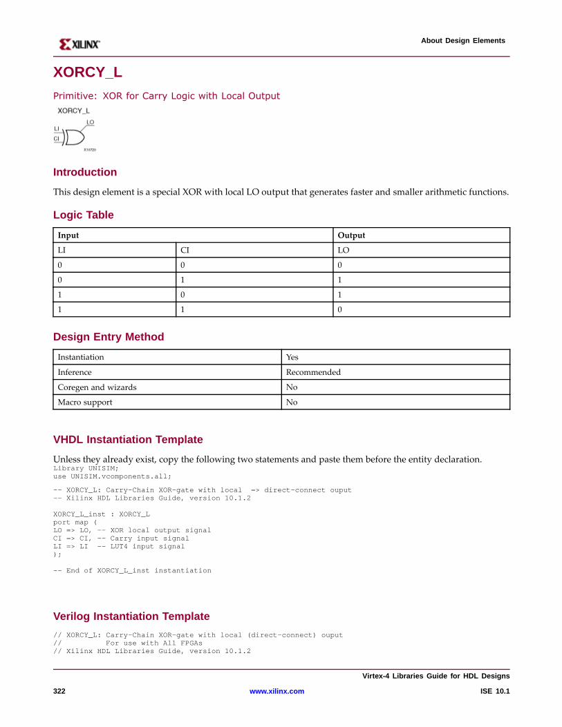
About Design Elements
XORCY_L
Primitive: XOR for Carry Logic with Local Output
Intr oduction
This design element is a special XOR with local LO output that generates faster and smaller arithmetic functions.
Logic Table
Input Output
LI CI LO
0 0 0
0 1 1
1 0 1
1 1 0
Design Entr y Method
Instantiation Yes
Inference Recommended
Coregen and wizards No
Macro support No
VHDL Instantiation Template
Unless they already exist, copy the following two statements and paste them before the entity declaration.Library UNISIM;use UNISIM.vcomponents.all;
-- XORCY_L: Carry-Chain XOR-gate with local => direct-connect ouput-- Xilinx HDL Libraries Guide, version 10.1.2
XORCY_L_inst : XORCY_Lport map (LO => LO, -- XOR local output signalCI => CI, -- Carry input signalLI => LI -- LUT4 input signal);
-- End of XORCY_L_inst instantiation
Verilog Instantiation Template
// XORCY_L: Carry-Chain XOR-gate with local (direct-connect) ouput// For use with All FPGAs// Xilinx HDL Libraries Guide, version 10.1.2
Vir tex-4 Libraries Guide for HDL Designs
322 www.xilinx.com ISE 10.1
About Design Elements
XORCY_LXORCY_L_inst (.LO(LO), // XOR local output signal.CI(CI), // Carry input signal.LI(LI) // LUT4 input signal);
// End of XORCY_L_inst instantiation
For More Information
• See the Virtex-4 User Guide.
• See the Virtex-4 Data Sheets.
Vir tex-4 Libraries Guide for HDL Designs
ISE 10.1 www.xilinx.com 323