
Xilinx Spartan-3E Libraries Guide for Schematic Designs · Spartan-3E Libraries Guide for Schematic...
783
Spartan-3E Libraries Guide for Schematic Designs UG618 (v 12.1) April 19, 2010
-
Upload
truongdang -
Category
Documents
-
view
248 -
download
2
Transcript of Xilinx Spartan-3E Libraries Guide for Schematic Designs · Spartan-3E Libraries Guide for Schematic...
Spartan-3E Libraries Guide forSchematic Designs
UG618 (v 12.1) April 19, 2010

Xilinx is disclosing this user guide, manual, release note, and/or specification (the “Documentation”) to yousolely for use in the development of designs to operate with Xilinx hardware devices. You may not reproduce,distribute, republish, download, display, post, or transmit the Documentation in any form or by any meansincluding, but not limited to, electronic, mechanical, photocopying, recording, or otherwise, without the priorwritten consent of Xilinx. Xilinx expressly disclaims any liability arising out of your use of the Documentation.Xilinx reserves the right, at its sole discretion, to change the Documentation without notice at any time. Xilinxassumes no obligation to correct any errors contained in the Documentation, or to advise you of any correctionsor updates. Xilinx expressly disclaims any liability in connection with technical support or assistance that may beprovided to you in connection with the Information.
THE DOCUMENTATION IS DISCLOSED TO YOU “AS-IS” WITH NOWARRANTY OF ANY KIND. XILINXMAKES NO OTHER WARRANTIES, WHETHER EXPRESS, IMPLIED, OR STATUTORY, REGARDINGTHE DOCUMENTATION, INCLUDING ANY WARRANTIES OF MERCHANTABILITY, FITNESS FOR APARTICULAR PURPOSE, OR NONINFRINGEMENT OF THIRD-PARTY RIGHTS. IN NO EVENT WILLXILINX BE LIABLE FOR ANY CONSEQUENTIAL, INDIRECT, EXEMPLARY, SPECIAL, OR INCIDENTALDAMAGES, INCLUDING ANY LOSS OF DATA OR LOST PROFITS, ARISING FROM YOUR USE OF THEDOCUMENTATION.
© Copyright 2002-2010 Xilinx Inc. All Rights Reserved. XILINX, the Xilinx logo, the Brand Window and otherdesignated brands included herein are trademarks of Xilinx, Inc. All other trademarks are the property oftheir respective owners.
Spartan-3E Libraries Guide for Schematic Designs2 www.xilinx.com UG618 (v 12.1) April 19, 2010
Preface
About this GuideThis schematic guide is part of the ISE documentation collection. A separate version ofthis guide is available if you prefer to work with HDL.
This guide contains the following:
• Introduction.
• A list of design elements supported in this architecture, organized by functionalcategories.
• Individual descriptions of each available primitive.
About Design ElementsThis version of the Libraries Guide describes design elements available for thisarchitecture. There are several categories of design elements:
• Primitives - The simplest design elements in the Xilinx libraries. Primitives are thedesign element "atoms." Examples of Xilinx primitives are the simple buffer, BUF,and the D flip-flop with clock enable and clear, FDCE.
• Macros - The design element "molecules" of the Xilinx libraries. Macros can becreated from the design element primitives or macros. For example, the FD4CEflip-flop macro is a composite of 4 FDCE primitives.
Xilinx maintains software libraries with hundreds of functional design elements(macros and primitives) for different device architectures. New functional elements areassembled with each release of development system software. This guide is one ina series of architecture-specific libraries.
Spartan-3E Libraries Guide for Schematic DesignsUG618 (v 12.1) April 19, 2010 www.xilinx.com 3
Table of ContentsPreface About this Guide ............................................................................................3
About Design Elements ......................................................................................... 3
Chapter 1 Functional Categories ..............................................................................17Chapter 2 About Design Elements ...........................................................................39
ACC16 ................................................................................................................... 40ACC4..................................................................................................................... 42ACC8..................................................................................................................... 44ADD16 .................................................................................................................. 46ADD4 .................................................................................................................... 47ADD8 .................................................................................................................... 48ADSU16 ................................................................................................................ 49ADSU4 .................................................................................................................. 51ADSU8 .................................................................................................................. 53AND12 .................................................................................................................. 55AND16 .................................................................................................................. 56AND2 .................................................................................................................... 57AND2B1................................................................................................................ 58AND2B2................................................................................................................ 59AND3 .................................................................................................................... 60AND3B1................................................................................................................ 61AND3B2................................................................................................................ 62AND3B3................................................................................................................ 63AND4 .................................................................................................................... 64AND4B1................................................................................................................ 65AND4B2................................................................................................................ 66AND4B3................................................................................................................ 67AND4B4................................................................................................................ 68AND5 .................................................................................................................... 69AND5B1................................................................................................................ 70AND5B2................................................................................................................ 71AND5B3................................................................................................................ 72AND5B4................................................................................................................ 73AND5B5................................................................................................................ 74AND6 .................................................................................................................... 75AND7 .................................................................................................................... 76
Spartan-3E Libraries Guide for Schematic Designs4 www.xilinx.com UG618 (v 12.1) April 19, 2010
AND8 .................................................................................................................... 77AND9 .................................................................................................................... 78BRLSHFT4............................................................................................................ 79BRLSHFT8............................................................................................................ 80BSCAN_SPARTAN3 ............................................................................................ 81BUF........................................................................................................................ 83BUFCF................................................................................................................... 84BUFG .................................................................................................................... 85BUFGCE................................................................................................................ 86BUFGCE_1............................................................................................................ 87BUFGMUX ........................................................................................................... 88BUFGMUX_1........................................................................................................ 89CAPTURE_SPARTAN3........................................................................................ 90CB16CE ................................................................................................................. 91CB16CLE ............................................................................................................... 93CB16CLED............................................................................................................ 95CB16RE ................................................................................................................. 97CB2CE ................................................................................................................... 98CB2CLE................................................................................................................. 99CB2CLED............................................................................................................ 101CB2RE ................................................................................................................. 103CB4CE ................................................................................................................. 104CB4CLE............................................................................................................... 105CB4CLED............................................................................................................ 107CB4RE ................................................................................................................. 109CB8CE ................................................................................................................. 110CB8CLE............................................................................................................... 112CB8CLED............................................................................................................ 114CB8RE ................................................................................................................. 116CC16CE ............................................................................................................... 117CC16CLE............................................................................................................. 118CC16CLED.......................................................................................................... 120CC16RE ............................................................................................................... 122CC8CE................................................................................................................. 123CC8CLE............................................................................................................... 124CC8CLED............................................................................................................ 126CC8RE................................................................................................................. 128CD4CE ................................................................................................................ 129
Spartan-3E Libraries Guide for Schematic DesignsUG618 (v 12.1) April 19, 2010 www.xilinx.com 5
CD4CLE .............................................................................................................. 131CD4RE ................................................................................................................ 133CD4RLE .............................................................................................................. 135CJ4CE .................................................................................................................. 137CJ4RE .................................................................................................................. 138CJ5CE .................................................................................................................. 139CJ5RE .................................................................................................................. 140CJ8CE .................................................................................................................. 141CJ8RE .................................................................................................................. 142COMP16.............................................................................................................. 143COMP2 ............................................................................................................... 144COMP4 ............................................................................................................... 145COMP8 ............................................................................................................... 146COMPM16.......................................................................................................... 147COMPM2............................................................................................................ 149COMPM4............................................................................................................ 150COMPM8............................................................................................................ 151COMPMC16 ....................................................................................................... 153COMPMC8 ......................................................................................................... 155CR16CE ............................................................................................................... 157CR8CE................................................................................................................. 158D2_4E .................................................................................................................. 159D3_8E .................................................................................................................. 160D4_16E ................................................................................................................ 161DCM_SP ............................................................................................................. 162DEC_CC16 .......................................................................................................... 167DEC_CC4............................................................................................................ 169DEC_CC8............................................................................................................ 170DECODE16......................................................................................................... 171DECODE32......................................................................................................... 172DECODE4........................................................................................................... 173DECODE64......................................................................................................... 174DECODE8........................................................................................................... 175FD........................................................................................................................ 176FD_1 .................................................................................................................... 177FD16CE ............................................................................................................... 178FD16RE ............................................................................................................... 179FD4CE ................................................................................................................. 180
Spartan-3E Libraries Guide for Schematic Designs6 www.xilinx.com UG618 (v 12.1) April 19, 2010
FD4RE ................................................................................................................. 181FD8CE ................................................................................................................. 182FD8RE ................................................................................................................. 183FDC ..................................................................................................................... 184FDC_1 ................................................................................................................. 185FDCE................................................................................................................... 186FDCE_1 ............................................................................................................... 187FDCP................................................................................................................... 188FDCP_1 ............................................................................................................... 189FDCPE................................................................................................................. 190FDCPE_1 ............................................................................................................. 192FDE...................................................................................................................... 194FDE_1.................................................................................................................. 195FDP...................................................................................................................... 196FDP_1.................................................................................................................. 197FDPE ................................................................................................................... 198FDPE_1................................................................................................................ 199FDR ..................................................................................................................... 200FDR_1 ................................................................................................................. 201FDRE................................................................................................................... 202FDRE_1 ............................................................................................................... 203FDRS................................................................................................................... 204FDRS_1 ............................................................................................................... 205FDRSE................................................................................................................. 206FDRSE_1 ............................................................................................................. 207FDS ..................................................................................................................... 208FDS_1.................................................................................................................. 209FDSE ................................................................................................................... 210FDSE_1................................................................................................................ 211FJKC.................................................................................................................... 212FJKCE.................................................................................................................. 213FJKP .................................................................................................................... 214FJKPE .................................................................................................................. 215FJKRSE ............................................................................................................... 217FJKSRE ............................................................................................................... 219FTC...................................................................................................................... 221FTCE ................................................................................................................... 222FTCLE ................................................................................................................. 223
Spartan-3E Libraries Guide for Schematic DesignsUG618 (v 12.1) April 19, 2010 www.xilinx.com 7
FTCLEX............................................................................................................... 224FTP ...................................................................................................................... 225FTPE.................................................................................................................... 226FTPLE.................................................................................................................. 227FTRSE ................................................................................................................. 229FTRSLE ............................................................................................................... 230FTSRE ................................................................................................................. 232FTSRLE ............................................................................................................... 233GND.................................................................................................................... 235IBUF .................................................................................................................... 236IBUF16 ................................................................................................................ 237IBUF4 .................................................................................................................. 238IBUF8 .................................................................................................................. 239IBUFDS............................................................................................................... 240IBUFG................................................................................................................. 242IBUFGDS............................................................................................................ 243IDDR2................................................................................................................. 245IFD ...................................................................................................................... 247IFD_1................................................................................................................... 248IFD16................................................................................................................... 249IFD4 .................................................................................................................... 250IFD8 .................................................................................................................... 251IFDI..................................................................................................................... 252IFDI_1 ................................................................................................................. 253IFDX.................................................................................................................... 254IFDX_1 ................................................................................................................ 255IFDX16 ................................................................................................................ 256IFDX4 .................................................................................................................. 257IFDX8 .................................................................................................................. 258IFDXI .................................................................................................................. 259IFDXI_1............................................................................................................... 260ILD ...................................................................................................................... 261ILD_1 .................................................................................................................. 262ILD16 .................................................................................................................. 263ILD4 .................................................................................................................... 264ILD8 .................................................................................................................... 265ILDI..................................................................................................................... 266ILDI_1 ................................................................................................................. 267
Spartan-3E Libraries Guide for Schematic Designs8 www.xilinx.com UG618 (v 12.1) April 19, 2010
ILDX.................................................................................................................... 268ILDX_1 ................................................................................................................ 269ILDX16 ................................................................................................................ 270ILDX4.................................................................................................................. 271ILDX8.................................................................................................................. 272ILDXI .................................................................................................................. 273ILDXI_1............................................................................................................... 274INV ..................................................................................................................... 275INV16.................................................................................................................. 276INV4.................................................................................................................... 277INV8.................................................................................................................... 278IOBUF ................................................................................................................. 279IOBUFDS............................................................................................................ 281KEEPER .............................................................................................................. 283LD........................................................................................................................ 284LD_1.................................................................................................................... 285LD16.................................................................................................................... 286LD16CE ............................................................................................................... 287LD4...................................................................................................................... 288LD4CE................................................................................................................. 289LD8...................................................................................................................... 290LD8CE................................................................................................................. 291LDC..................................................................................................................... 292LDC_1 ................................................................................................................. 293LDCE................................................................................................................... 294LDCE_1 ............................................................................................................... 295LDCP................................................................................................................... 296LDCP_1 ............................................................................................................... 297LDCPE ................................................................................................................ 298LDCPE_1............................................................................................................. 300LDE ..................................................................................................................... 301LDE_1.................................................................................................................. 302LDP ..................................................................................................................... 303LDP_1.................................................................................................................. 304LDPE ................................................................................................................... 305LDPE_1 ............................................................................................................... 306LUT1 ................................................................................................................... 307LUT1_D............................................................................................................... 309
Spartan-3E Libraries Guide for Schematic DesignsUG618 (v 12.1) April 19, 2010 www.xilinx.com 9
LUT1_L ............................................................................................................... 310LUT2 ................................................................................................................... 311LUT2_D............................................................................................................... 313LUT2_L ............................................................................................................... 315LUT3 ................................................................................................................... 317LUT3_D............................................................................................................... 319LUT3_L ............................................................................................................... 321LUT4 ................................................................................................................... 323LUT4_D............................................................................................................... 325LUT4_L ............................................................................................................... 327M16_1E................................................................................................................ 329M2_1.................................................................................................................... 331M2_1B1 ............................................................................................................... 332M2_1B2 ............................................................................................................... 333M2_1E ................................................................................................................. 334M4_1E ................................................................................................................. 335M8_1E ................................................................................................................. 336MULT_AND ....................................................................................................... 337MULT18X18 ........................................................................................................ 338MULT18X18S...................................................................................................... 339MULT18X18SIO ................................................................................................. 340MUXCY............................................................................................................... 341MUXCY_D.......................................................................................................... 342MUXCY_L........................................................................................................... 343MUXF5 ................................................................................................................ 344MUXF5_D ........................................................................................................... 345MUXF5_L............................................................................................................ 346MUXF6 ................................................................................................................ 347MUXF6_D ........................................................................................................... 348MUXF6_L............................................................................................................ 349MUXF7 ................................................................................................................ 350MUXF7_D ........................................................................................................... 351MUXF7_L............................................................................................................ 352MUXF8 ................................................................................................................ 353MUXF8_D ........................................................................................................... 354MUXF8_L............................................................................................................ 355NAND12 ............................................................................................................. 356NAND16 ............................................................................................................. 357
Spartan-3E Libraries Guide for Schematic Designs10 www.xilinx.com UG618 (v 12.1) April 19, 2010
NAND2............................................................................................................... 358NAND2B1........................................................................................................... 359NAND2B2........................................................................................................... 360NAND3............................................................................................................... 361NAND3B1........................................................................................................... 362NAND3B2........................................................................................................... 363NAND3B3........................................................................................................... 364NAND4............................................................................................................... 365NAND4B1........................................................................................................... 366NAND4B2........................................................................................................... 367NAND4B3........................................................................................................... 368NAND4B4........................................................................................................... 369NAND5............................................................................................................... 370NAND5B1........................................................................................................... 371NAND5B2........................................................................................................... 372NAND5B3........................................................................................................... 373NAND5B4........................................................................................................... 374NAND5B5........................................................................................................... 375NAND6............................................................................................................... 376NAND7............................................................................................................... 377NAND8............................................................................................................... 378NAND9............................................................................................................... 379NOR12 ................................................................................................................ 380NOR16 ................................................................................................................ 381NOR2 .................................................................................................................. 382NOR2B1 .............................................................................................................. 383NOR2B2 .............................................................................................................. 384NOR3 .................................................................................................................. 385NOR3B1 .............................................................................................................. 386NOR3B2 .............................................................................................................. 387NOR3B3 .............................................................................................................. 388NOR4 .................................................................................................................. 389NOR4B1 .............................................................................................................. 390NOR4B2 .............................................................................................................. 391NOR4B3 .............................................................................................................. 392NOR4B4 .............................................................................................................. 393NOR5 .................................................................................................................. 394NOR5B1 .............................................................................................................. 395
Spartan-3E Libraries Guide for Schematic DesignsUG618 (v 12.1) April 19, 2010 www.xilinx.com 11
NOR5B2 .............................................................................................................. 396NOR5B3 .............................................................................................................. 397NOR5B4 .............................................................................................................. 398NOR5B5 .............................................................................................................. 399NOR6 .................................................................................................................. 400NOR7 .................................................................................................................. 401NOR8 .................................................................................................................. 402NOR9 .................................................................................................................. 403OBUF .................................................................................................................. 404OBUF16............................................................................................................... 405OBUF4................................................................................................................. 406OBUF8................................................................................................................. 407OBUFDS ............................................................................................................. 408OBUFT ................................................................................................................ 409OBUFT16 ............................................................................................................ 411OBUFT4 .............................................................................................................. 412OBUFT8 .............................................................................................................. 413OBUFTDS........................................................................................................... 414ODDR2 ............................................................................................................... 415OFD..................................................................................................................... 417OFD_1 ................................................................................................................. 418OFD16 ................................................................................................................. 419OFD4................................................................................................................... 420OFD8................................................................................................................... 421OFDE .................................................................................................................. 422OFDE_1............................................................................................................... 423OFDE16............................................................................................................... 424OFDE4................................................................................................................. 425OFDE8................................................................................................................. 426OFDI ................................................................................................................... 427OFDI_1................................................................................................................ 428OFDT .................................................................................................................. 429OFDT_1............................................................................................................... 430OFDT16............................................................................................................... 431OFDT4 ................................................................................................................ 432OFDT8 ................................................................................................................ 433OFDX .................................................................................................................. 434OFDX_1............................................................................................................... 435
Spartan-3E Libraries Guide for Schematic Designs12 www.xilinx.com UG618 (v 12.1) April 19, 2010
OFDX16............................................................................................................... 436OFDX4 ................................................................................................................ 437OFDX8 ................................................................................................................ 438OFDXI................................................................................................................. 439OFDXI_1 ............................................................................................................. 440OR12 ................................................................................................................... 441OR16 ................................................................................................................... 442OR2 ..................................................................................................................... 443OR2B1 ................................................................................................................. 444OR2B2 ................................................................................................................. 445OR3 ..................................................................................................................... 446OR3B1 ................................................................................................................. 447OR3B2 ................................................................................................................. 448OR3B3 ................................................................................................................. 449OR4 ..................................................................................................................... 450OR4B1 ................................................................................................................. 451OR4B2 ................................................................................................................. 452OR4B3 ................................................................................................................. 453OR4B4 ................................................................................................................. 454OR5 ..................................................................................................................... 455OR5B1 ................................................................................................................. 456OR5B2 ................................................................................................................. 457OR5B3 ................................................................................................................. 458OR5B4 ................................................................................................................. 459OR5B5 ................................................................................................................. 460OR6 ..................................................................................................................... 461OR7 ..................................................................................................................... 462OR8 ..................................................................................................................... 463OR9 ..................................................................................................................... 464PULLDOWN ...................................................................................................... 465PULLUP .............................................................................................................. 466RAM16X1D......................................................................................................... 467RAM16X1D_1 ..................................................................................................... 469RAM16X1S.......................................................................................................... 471RAM16X1S_1...................................................................................................... 472RAM16X2S.......................................................................................................... 474RAM16X4S.......................................................................................................... 476RAM16X8S.......................................................................................................... 478
Spartan-3E Libraries Guide for Schematic DesignsUG618 (v 12.1) April 19, 2010 www.xilinx.com 13
RAM32X1S.......................................................................................................... 480RAM32X1S_1...................................................................................................... 481RAM32X2S.......................................................................................................... 482RAM32X4S.......................................................................................................... 484RAM32X8S.......................................................................................................... 486RAM64X1S.......................................................................................................... 488RAM64X1S_1...................................................................................................... 490RAM64X2S.......................................................................................................... 491RAMB16_S1........................................................................................................ 493RAMB16_S1_S1.................................................................................................. 497RAMB16_S1_S18 ................................................................................................ 507RAMB16_S1_S2.................................................................................................. 516RAMB16_S1_S36 ................................................................................................ 525RAMB16_S1_S4.................................................................................................. 534RAMB16_S1_S9.................................................................................................. 543RAMB16_S18...................................................................................................... 551RAMB16_S18_S18 .............................................................................................. 554RAMB16_S18_S36 .............................................................................................. 562RAMB16_S2........................................................................................................ 570RAMB16_S2_S18 ................................................................................................ 574RAMB16_S2_S2.................................................................................................. 583RAMB16_S2_S36 ................................................................................................ 592RAMB16_S2_S4.................................................................................................. 601RAMB16_S2_S9.................................................................................................. 609RAMB16_S36...................................................................................................... 617RAMB16_S36_S36 .............................................................................................. 621RAMB16_S4........................................................................................................ 629RAMB16_S4_S18 ................................................................................................ 633RAMB16_S4_S36 ................................................................................................ 642RAMB16_S4_S4.................................................................................................. 651RAMB16_S4_S9.................................................................................................. 660RAMB16_S9........................................................................................................ 668RAMB16_S9_S18 ................................................................................................ 671RAMB16_S9_S36 ................................................................................................ 679RAMB16_S9_S9.................................................................................................. 687ROM128X1.......................................................................................................... 695ROM16X1............................................................................................................ 697ROM256X1.......................................................................................................... 699
Spartan-3E Libraries Guide for Schematic Designs14 www.xilinx.com UG618 (v 12.1) April 19, 2010
ROM32X1............................................................................................................ 701ROM64X1............................................................................................................ 703SOP3 ................................................................................................................... 705SOP3B1A ............................................................................................................ 706SOP3B1B............................................................................................................. 707SOP3B2A ............................................................................................................ 708SOP3B2B............................................................................................................. 709SOP3B3 ............................................................................................................... 710SOP4 ................................................................................................................... 711SOP4B1 ............................................................................................................... 712SOP4B2A ............................................................................................................ 713SOP4B2B............................................................................................................. 714SOP4B3 ............................................................................................................... 715SOP4B4 ............................................................................................................... 716SR16CE ............................................................................................................... 717SR16CLE ............................................................................................................. 718SR16CLED .......................................................................................................... 720SR16RE ............................................................................................................... 722SR16RLE ............................................................................................................. 723SR16RLED .......................................................................................................... 725SR4CE ................................................................................................................. 727SR4CLE ............................................................................................................... 728SR4CLED............................................................................................................ 730SR4RE ................................................................................................................. 732SR4RLE ............................................................................................................... 733SR4RLED............................................................................................................ 735SR8CE ................................................................................................................. 737SR8CLE ............................................................................................................... 738SR8CLED............................................................................................................ 740SR8RE ................................................................................................................. 742SR8RLE ............................................................................................................... 743SR8RLED............................................................................................................ 745SRL16 .................................................................................................................. 747SRL16_1 .............................................................................................................. 749SRL16E................................................................................................................ 751SRL16E_1 ............................................................................................................ 753SRLC16 ............................................................................................................... 755SRLC16_1............................................................................................................ 757
Spartan-3E Libraries Guide for Schematic DesignsUG618 (v 12.1) April 19, 2010 www.xilinx.com 15
SRLC16E ............................................................................................................. 759SRLC16E_1.......................................................................................................... 761STARTUP_SPARTAN3E .................................................................................... 763VCC..................................................................................................................... 764XNOR2................................................................................................................ 765XNOR3................................................................................................................ 766XNOR4................................................................................................................ 767XNOR5................................................................................................................ 768XNOR6................................................................................................................ 769XNOR7................................................................................................................ 770XNOR8................................................................................................................ 771XNOR9................................................................................................................ 772XOR2................................................................................................................... 773XOR3................................................................................................................... 774XOR4................................................................................................................... 775XOR5................................................................................................................... 776XOR6................................................................................................................... 777XOR7................................................................................................................... 778XOR8................................................................................................................... 779XOR9................................................................................................................... 780XORCY................................................................................................................ 781XORCY_D........................................................................................................... 782XORCY_L............................................................................................................ 783
Spartan-3E Libraries Guide for Schematic Designs16 www.xilinx.com UG618 (v 12.1) April 19, 2010
Chapter 1
Functional CategoriesThis section categorizes, by function, the circuit design elements described in detail laterin this guide. The elements ( primitives and macros) are listed in alphanumeric orderunder each functional category.
Arithmetic Flip Flop LUT
Buffer General Memory
Carry Logic IO Mux
Comparator IO FlipFlop Shift Register
Counter IO Latch Shifter
DDR Flip Flop Latch
Decoder Logic
Spartan-3E Libraries Guide for Schematic DesignsUG618 (v 12.1) April 19, 2010 www.xilinx.com 17
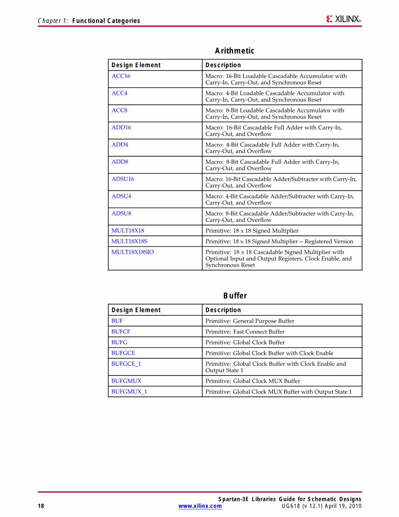
Chapter 1: Functional Categories
ArithmeticDesign Element DescriptionACC16 Macro: 16-Bit Loadable Cascadable Accumulator with
Carry-In, Carry-Out, and Synchronous Reset
ACC4 Macro: 4-Bit Loadable Cascadable Accumulator withCarry-In, Carry-Out, and Synchronous Reset
ACC8 Macro: 8-Bit Loadable Cascadable Accumulator withCarry-In, Carry-Out, and Synchronous Reset
ADD16 Macro: 16-Bit Cascadable Full Adder with Carry-In,Carry-Out, and Overflow
ADD4 Macro: 4-Bit Cascadable Full Adder with Carry-In,Carry-Out, and Overflow
ADD8 Macro: 8-Bit Cascadable Full Adder with Carry-In,Carry-Out, and Overflow
ADSU16 Macro: 16-Bit Cascadable Adder/Subtracter with Carry-In,Carry-Out, and Overflow
ADSU4 Macro: 4-Bit Cascadable Adder/Subtracter with Carry-In,Carry-Out, and Overflow
ADSU8 Macro: 8-Bit Cascadable Adder/Subtracter with Carry-In,Carry-Out, and Overflow
MULT18X18 Primitive: 18 x 18 Signed Multiplier
MULT18X18S Primitive: 18 x 18 Signed Multiplier -- Registered Version
MULT18X18SIO Primitive: 18 x 18 Cascadable Signed Multiplier withOptional Input and Output Registers, Clock Enable, andSynchronous Reset
BufferDesign Element DescriptionBUF Primitive: General Purpose Buffer
BUFCF Primitive: Fast Connect Buffer
BUFG Primitive: Global Clock Buffer
BUFGCE Primitive: Global Clock Buffer with Clock Enable
BUFGCE_1 Primitive: Global Clock Buffer with Clock Enable andOutput State 1
BUFGMUX Primitive: Global Clock MUX Buffer
BUFGMUX_1 Primitive: Global Clock MUX Buffer with Output State 1
Spartan-3E Libraries Guide for Schematic Designs18 www.xilinx.com UG618 (v 12.1) April 19, 2010
Chapter 1: Functional Categories
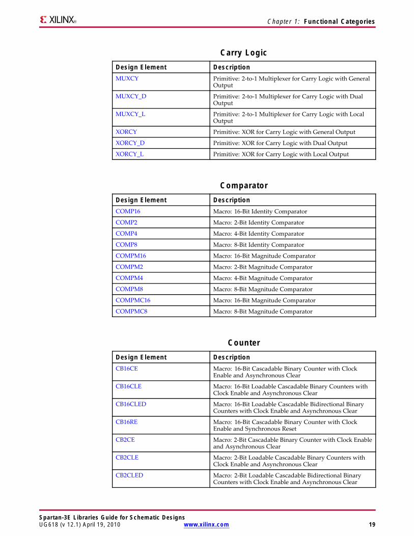
Carry LogicDesign Element DescriptionMUXCY Primitive: 2-to-1 Multiplexer for Carry Logic with General
Output
MUXCY_D Primitive: 2-to-1 Multiplexer for Carry Logic with DualOutput
MUXCY_L Primitive: 2-to-1 Multiplexer for Carry Logic with LocalOutput
XORCY Primitive: XOR for Carry Logic with General Output
XORCY_D Primitive: XOR for Carry Logic with Dual Output
XORCY_L Primitive: XOR for Carry Logic with Local Output
ComparatorDesign Element DescriptionCOMP16 Macro: 16-Bit Identity Comparator
COMP2 Macro: 2-Bit Identity Comparator
COMP4 Macro: 4-Bit Identity Comparator
COMP8 Macro: 8-Bit Identity Comparator
COMPM16 Macro: 16-Bit Magnitude Comparator
COMPM2 Macro: 2-Bit Magnitude Comparator
COMPM4 Macro: 4-Bit Magnitude Comparator
COMPM8 Macro: 8-Bit Magnitude Comparator
COMPMC16 Macro: 16-Bit Magnitude Comparator
COMPMC8 Macro: 8-Bit Magnitude Comparator
CounterDesign Element DescriptionCB16CE Macro: 16-Bit Cascadable Binary Counter with Clock
Enable and Asynchronous Clear
CB16CLE Macro: 16-Bit Loadable Cascadable Binary Counters withClock Enable and Asynchronous Clear
CB16CLED Macro: 16-Bit Loadable Cascadable Bidirectional BinaryCounters with Clock Enable and Asynchronous Clear
CB16RE Macro: 16-Bit Cascadable Binary Counter with ClockEnable and Synchronous Reset
CB2CE Macro: 2-Bit Cascadable Binary Counter with Clock Enableand Asynchronous Clear
CB2CLE Macro: 2-Bit Loadable Cascadable Binary Counters withClock Enable and Asynchronous Clear
CB2CLED Macro: 2-Bit Loadable Cascadable Bidirectional BinaryCounters with Clock Enable and Asynchronous Clear
Spartan-3E Libraries Guide for Schematic DesignsUG618 (v 12.1) April 19, 2010 www.xilinx.com 19
Chapter 1: Functional Categories
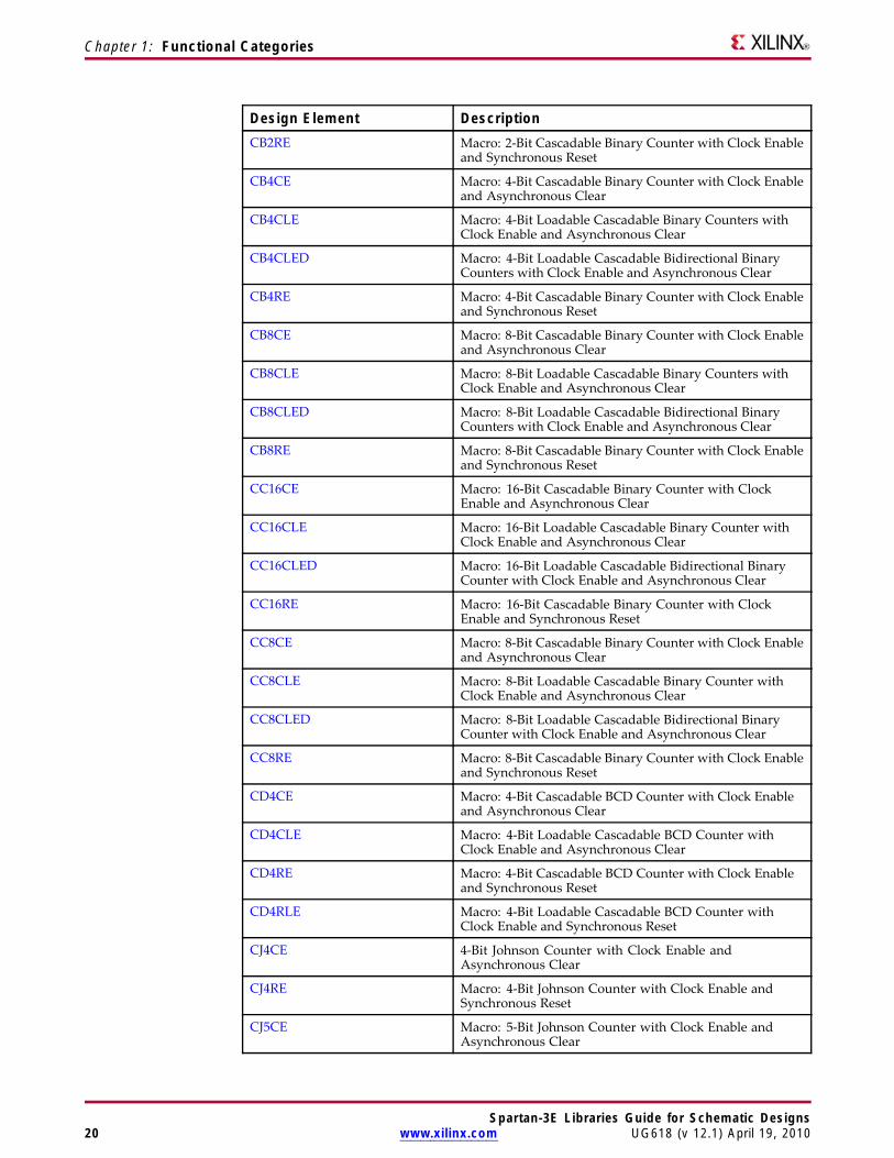
Design Element DescriptionCB2RE Macro: 2-Bit Cascadable Binary Counter with Clock Enable
and Synchronous Reset
CB4CE Macro: 4-Bit Cascadable Binary Counter with Clock Enableand Asynchronous Clear
CB4CLE Macro: 4-Bit Loadable Cascadable Binary Counters withClock Enable and Asynchronous Clear
CB4CLED Macro: 4-Bit Loadable Cascadable Bidirectional BinaryCounters with Clock Enable and Asynchronous Clear
CB4RE Macro: 4-Bit Cascadable Binary Counter with Clock Enableand Synchronous Reset
CB8CE Macro: 8-Bit Cascadable Binary Counter with Clock Enableand Asynchronous Clear
CB8CLE Macro: 8-Bit Loadable Cascadable Binary Counters withClock Enable and Asynchronous Clear
CB8CLED Macro: 8-Bit Loadable Cascadable Bidirectional BinaryCounters with Clock Enable and Asynchronous Clear
CB8RE Macro: 8-Bit Cascadable Binary Counter with Clock Enableand Synchronous Reset
CC16CE Macro: 16-Bit Cascadable Binary Counter with ClockEnable and Asynchronous Clear
CC16CLE Macro: 16-Bit Loadable Cascadable Binary Counter withClock Enable and Asynchronous Clear
CC16CLED Macro: 16-Bit Loadable Cascadable Bidirectional BinaryCounter with Clock Enable and Asynchronous Clear
CC16RE Macro: 16-Bit Cascadable Binary Counter with ClockEnable and Synchronous Reset
CC8CE Macro: 8-Bit Cascadable Binary Counter with Clock Enableand Asynchronous Clear
CC8CLE Macro: 8-Bit Loadable Cascadable Binary Counter withClock Enable and Asynchronous Clear
CC8CLED Macro: 8-Bit Loadable Cascadable Bidirectional BinaryCounter with Clock Enable and Asynchronous Clear
CC8RE Macro: 8-Bit Cascadable Binary Counter with Clock Enableand Synchronous Reset
CD4CE Macro: 4-Bit Cascadable BCD Counter with Clock Enableand Asynchronous Clear
CD4CLE Macro: 4-Bit Loadable Cascadable BCD Counter withClock Enable and Asynchronous Clear
CD4RE Macro: 4-Bit Cascadable BCD Counter with Clock Enableand Synchronous Reset
CD4RLE Macro: 4-Bit Loadable Cascadable BCD Counter withClock Enable and Synchronous Reset
CJ4CE 4-Bit Johnson Counter with Clock Enable andAsynchronous Clear
CJ4RE Macro: 4-Bit Johnson Counter with Clock Enable andSynchronous Reset
CJ5CE Macro: 5-Bit Johnson Counter with Clock Enable andAsynchronous Clear
Spartan-3E Libraries Guide for Schematic Designs20 www.xilinx.com UG618 (v 12.1) April 19, 2010
Chapter 1: Functional Categories
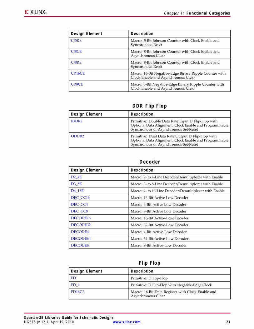
Design Element DescriptionCJ5RE Macro: 5-Bit Johnson Counter with Clock Enable and
Synchronous Reset
CJ8CE Macro: 8-Bit Johnson Counter with Clock Enable andAsynchronous Clear
CJ8RE Macro: 8-Bit Johnson Counter with Clock Enable andSynchronous Reset
CR16CE Macro: 16-Bit Negative-Edge Binary Ripple Counter withClock Enable and Asynchronous Clear
CR8CE Macro: 8-Bit Negative-Edge Binary Ripple Counter withClock Enable and Asynchronous Clear
DDR Flip FlopDesign Element DescriptionIDDR2 Primitive: Double Data Rate Input D Flip-Flop with
Optional Data Alignment, Clock Enable and ProgrammableSynchronous or Asynchronous Set/Reset
ODDR2 Primitive: Dual Data Rate Output D Flip-Flop withOptional Data Alignment, Clock Enable and ProgrammableSynchronous or Asynchronous Set/Reset
DecoderDesign Element DescriptionD2_4E Macro: 2- to 4-Line Decoder/Demultiplexer with Enable
D3_8E Macro: 3- to 8-Line Decoder/Demultiplexer with Enable
D4_16E Macro: 4- to 16-Line Decoder/Demultiplexer with Enable
DEC_CC16 Macro: 16-Bit Active Low Decoder
DEC_CC4 Macro: 4-Bit Active Low Decoder
DEC_CC8 Macro: 8-Bit Active Low Decoder
DECODE16 Macro: 16-Bit Active-Low Decoder
DECODE32 Macro: 32-Bit Active-Low Decoder
DECODE4 Macro: 4-Bit Active-Low Decoder
DECODE64 Macro: 64-Bit Active-Low Decoder
DECODE8 Macro: 8-Bit Active-Low Decoder
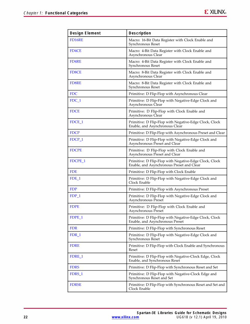
Flip FlopDesign Element DescriptionFD Primitive: D Flip-Flop
FD_1 Primitive: D Flip-Flop with Negative-Edge Clock
FD16CE Macro: 16-Bit Data Register with Clock Enable andAsynchronous Clear
Spartan-3E Libraries Guide for Schematic DesignsUG618 (v 12.1) April 19, 2010 www.xilinx.com 21
Chapter 1: Functional Categories
Design Element DescriptionFD16RE Macro: 16-Bit Data Register with Clock Enable and
Synchronous Reset
FD4CE Macro: 4-Bit Data Register with Clock Enable andAsynchronous Clear
FD4RE Macro: 4-Bit Data Register with Clock Enable andSynchronous Reset
FD8CE Macro: 8-Bit Data Register with Clock Enable andAsynchronous Clear
FD8RE Macro: 8-Bit Data Register with Clock Enable andSynchronous Reset
FDC Primitive: D Flip-Flop with Asynchronous Clear
FDC_1 Primitive: D Flip-Flop with Negative-Edge Clock andAsynchronous Clear
FDCE Primitive: D Flip-Flop with Clock Enable andAsynchronous Clear
FDCE_1 Primitive: D Flip-Flop with Negative-Edge Clock, ClockEnable, and Asynchronous Clear
FDCP Primitive: D Flip-Flop with Asynchronous Preset and Clear
FDCP_1 Primitive: D Flip-Flop with Negative-Edge Clock andAsynchronous Preset and Clear
FDCPE Primitive: D Flip-Flop with Clock Enable andAsynchronous Preset and Clear
FDCPE_1 Primitive: D Flip-Flop with Negative-Edge Clock, ClockEnable, and Asynchronous Preset and Clear
FDE Primitive: D Flip-Flop with Clock Enable
FDE_1 Primitive: D Flip-Flop with Negative-Edge Clock andClock Enable
FDP Primitive: D Flip-Flop with Asynchronous Preset
FDP_1 Primitive: D Flip-Flop with Negative-Edge Clock andAsynchronous Preset
FDPE Primitive: D Flip-Flop with Clock Enable andAsynchronous Preset
FDPE_1 Primitive: D Flip-Flop with Negative-Edge Clock, ClockEnable, and Asynchronous Preset
FDR Primitive: D Flip-Flop with Synchronous Reset
FDR_1 Primitive: D Flip-Flop with Negative-Edge Clock andSynchronous Reset
FDRE Primitive: D Flip-Flop with Clock Enable and SynchronousReset
FDRE_1 Primitive: D Flip-Flop with Negative-Clock Edge, ClockEnable, and Synchronous Reset
FDRS Primitive: D Flip-Flop with Synchronous Reset and Set
FDRS_1 Primitive: D Flip-Flop with Negative-Clock Edge andSynchronous Reset and Set
FDRSE Primitive: D Flip-Flop with Synchronous Reset and Set andClock Enable
Spartan-3E Libraries Guide for Schematic Designs22 www.xilinx.com UG618 (v 12.1) April 19, 2010
Chapter 1: Functional Categories
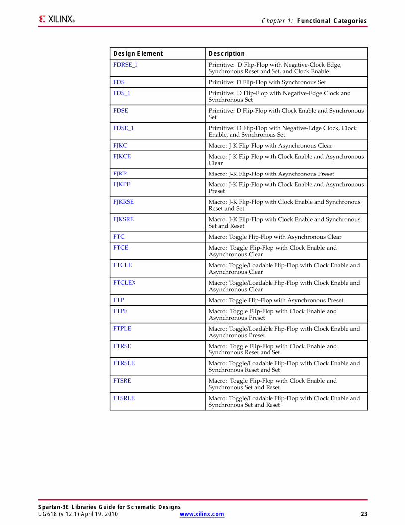
Design Element DescriptionFDRSE_1 Primitive: D Flip-Flop with Negative-Clock Edge,
Synchronous Reset and Set, and Clock Enable
FDS Primitive: D Flip-Flop with Synchronous Set
FDS_1 Primitive: D Flip-Flop with Negative-Edge Clock andSynchronous Set
FDSE Primitive: D Flip-Flop with Clock Enable and SynchronousSet
FDSE_1 Primitive: D Flip-Flop with Negative-Edge Clock, ClockEnable, and Synchronous Set
FJKC Macro: J-K Flip-Flop with Asynchronous Clear
FJKCE Macro: J-K Flip-Flop with Clock Enable and AsynchronousClear
FJKP Macro: J-K Flip-Flop with Asynchronous Preset
FJKPE Macro: J-K Flip-Flop with Clock Enable and AsynchronousPreset
FJKRSE Macro: J-K Flip-Flop with Clock Enable and SynchronousReset and Set
FJKSRE Macro: J-K Flip-Flop with Clock Enable and SynchronousSet and Reset
FTC Macro: Toggle Flip-Flop with Asynchronous Clear
FTCE Macro: Toggle Flip-Flop with Clock Enable andAsynchronous Clear
FTCLE Macro: Toggle/Loadable Flip-Flop with Clock Enable andAsynchronous Clear
FTCLEX Macro: Toggle/Loadable Flip-Flop with Clock Enable andAsynchronous Clear
FTP Macro: Toggle Flip-Flop with Asynchronous Preset
FTPE Macro: Toggle Flip-Flop with Clock Enable andAsynchronous Preset
FTPLE Macro: Toggle/Loadable Flip-Flop with Clock Enable andAsynchronous Preset
FTRSE Macro: Toggle Flip-Flop with Clock Enable andSynchronous Reset and Set
FTRSLE Macro: Toggle/Loadable Flip-Flop with Clock Enable andSynchronous Reset and Set
FTSRE Macro: Toggle Flip-Flop with Clock Enable andSynchronous Set and Reset
FTSRLE Macro: Toggle/Loadable Flip-Flop with Clock Enable andSynchronous Set and Reset
Spartan-3E Libraries Guide for Schematic DesignsUG618 (v 12.1) April 19, 2010 www.xilinx.com 23
Chapter 1: Functional Categories
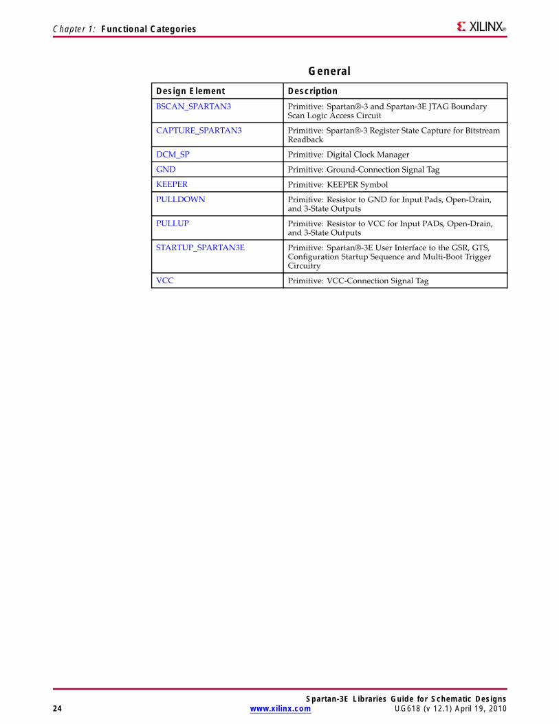
GeneralDesign Element DescriptionBSCAN_SPARTAN3 Primitive: Spartan®-3 and Spartan-3E JTAG Boundary
Scan Logic Access Circuit
CAPTURE_SPARTAN3 Primitive: Spartan®-3 Register State Capture for BitstreamReadback
DCM_SP Primitive: Digital Clock Manager
GND Primitive: Ground-Connection Signal Tag
KEEPER Primitive: KEEPER Symbol
PULLDOWN Primitive: Resistor to GND for Input Pads, Open-Drain,and 3-State Outputs
PULLUP Primitive: Resistor to VCC for Input PADs, Open-Drain,and 3-State Outputs
STARTUP_SPARTAN3E Primitive: Spartan®-3E User Interface to the GSR, GTS,Configuration Startup Sequence and Multi-Boot TriggerCircuitry
VCC Primitive: VCC-Connection Signal Tag
Spartan-3E Libraries Guide for Schematic Designs24 www.xilinx.com UG618 (v 12.1) April 19, 2010
Chapter 1: Functional Categories
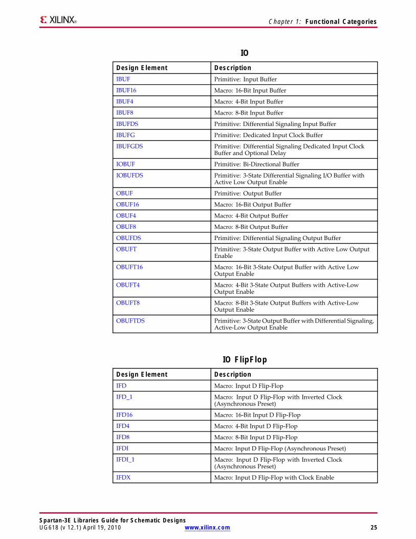
IODesign Element DescriptionIBUF Primitive: Input Buffer
IBUF16 Macro: 16-Bit Input Buffer
IBUF4 Macro: 4-Bit Input Buffer
IBUF8 Macro: 8-Bit Input Buffer
IBUFDS Primitive: Differential Signaling Input Buffer
IBUFG Primitive: Dedicated Input Clock Buffer
IBUFGDS Primitive: Differential Signaling Dedicated Input ClockBuffer and Optional Delay
IOBUF Primitive: Bi-Directional Buffer
IOBUFDS Primitive: 3-State Differential Signaling I/O Buffer withActive Low Output Enable
OBUF Primitive: Output Buffer
OBUF16 Macro: 16-Bit Output Buffer
OBUF4 Macro: 4-Bit Output Buffer
OBUF8 Macro: 8-Bit Output Buffer
OBUFDS Primitive: Differential Signaling Output Buffer
OBUFT Primitive: 3-State Output Buffer with Active Low OutputEnable
OBUFT16 Macro: 16-Bit 3-State Output Buffer with Active LowOutput Enable
OBUFT4 Macro: 4-Bit 3-State Output Buffers with Active-LowOutput Enable
OBUFT8 Macro: 8-Bit 3-State Output Buffers with Active-LowOutput Enable
OBUFTDS Primitive: 3-State Output Buffer with Differential Signaling,Active-Low Output Enable
IO FlipFlopDesign Element DescriptionIFD Macro: Input D Flip-Flop
IFD_1 Macro: Input D Flip-Flop with Inverted Clock(Asynchronous Preset)
IFD16 Macro: 16-Bit Input D Flip-Flop
IFD4 Macro: 4-Bit Input D Flip-Flop
IFD8 Macro: 8-Bit Input D Flip-Flop
IFDI Macro: Input D Flip-Flop (Asynchronous Preset)
IFDI_1 Macro: Input D Flip-Flop with Inverted Clock(Asynchronous Preset)
IFDX Macro: Input D Flip-Flop with Clock Enable
Spartan-3E Libraries Guide for Schematic DesignsUG618 (v 12.1) April 19, 2010 www.xilinx.com 25
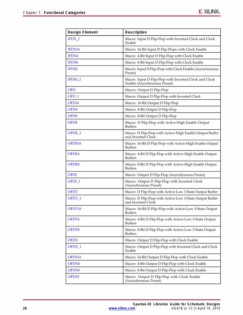
Chapter 1: Functional Categories
Design Element DescriptionIFDX_1 Macro: Input D Flip-Flop with Inverted Clock and Clock
Enable
IFDX16 Macro: 16-Bit Input D Flip-Flops with Clock Enable
IFDX4 Macro: 4-Bit Input D Flip-Flop with Clock Enable
IFDX8 Macro: 8-Bit Input D Flip-Flop with Clock Enable
IFDXI Macro: Input D Flip-Flopwith Clock Enable (AsynchronousPreset)
IFDXI_1 Macro: Input D Flip-Flop with Inverted Clock and ClockEnable (Asynchronous Preset)
OFD Macro: Output D Flip-Flop
OFD_1 Macro: Output D Flip-Flop with Inverted Clock
OFD16 Macro: 16-Bit Output D Flip-Flop
OFD4 Macro: 4-Bit Output D Flip-Flop
OFD8 Macro: 8-Bit Output D Flip-Flop
OFDE Macro: D Flip-Flop with Active-High Enable OutputBuffers
OFDE_1 Macro: D Flip-Flop with Active-High Enable Output Bufferand Inverted Clock
OFDE16 Macro: 16-Bit D Flip-Flop with Active-High Enable OutputBuffers
OFDE4 Macro: 4-Bit D Flip-Flop with Active-High Enable OutputBuffers
OFDE8 Macro: 8-Bit D Flip-Flop with Active-High Enable OutputBuffers
OFDI Macro: Output D Flip-Flop (Asynchronous Preset)
OFDI_1 Macro: Output D Flip-Flop with Inverted Clock(Asynchronous Preset)
OFDT Macro: D Flip-Flop with Active-Low 3-State Output Buffer
OFDT_1 Macro: D Flip-Flop with Active-Low 3-State Output Bufferand Inverted Clock
OFDT16 Macro: 16-Bit D Flip-Flop with Active-Low 3-State OutputBuffers
OFDT4 Macro: 4-Bit D Flip-Flop with Active-Low 3-State OutputBuffers
OFDT8 Macro: 8-Bit D Flip-Flop with Active-Low 3-State OutputBuffers
OFDX Macro: Output D Flip-Flop with Clock Enable
OFDX_1 Macro: Output D Flip-Flop with Inverted Clock and ClockEnable
OFDX16 Macro: 16-Bit Output D Flip-Flop with Clock Enable
OFDX4 Macro: 4-Bit Output D Flip-Flop with Clock Enable
OFDX8 Macro: 8-Bit Output D Flip-Flop with Clock Enable
OFDXI Macro: Output D Flip-Flop with Clock Enable(Asynchronous Preset)
Spartan-3E Libraries Guide for Schematic Designs26 www.xilinx.com UG618 (v 12.1) April 19, 2010
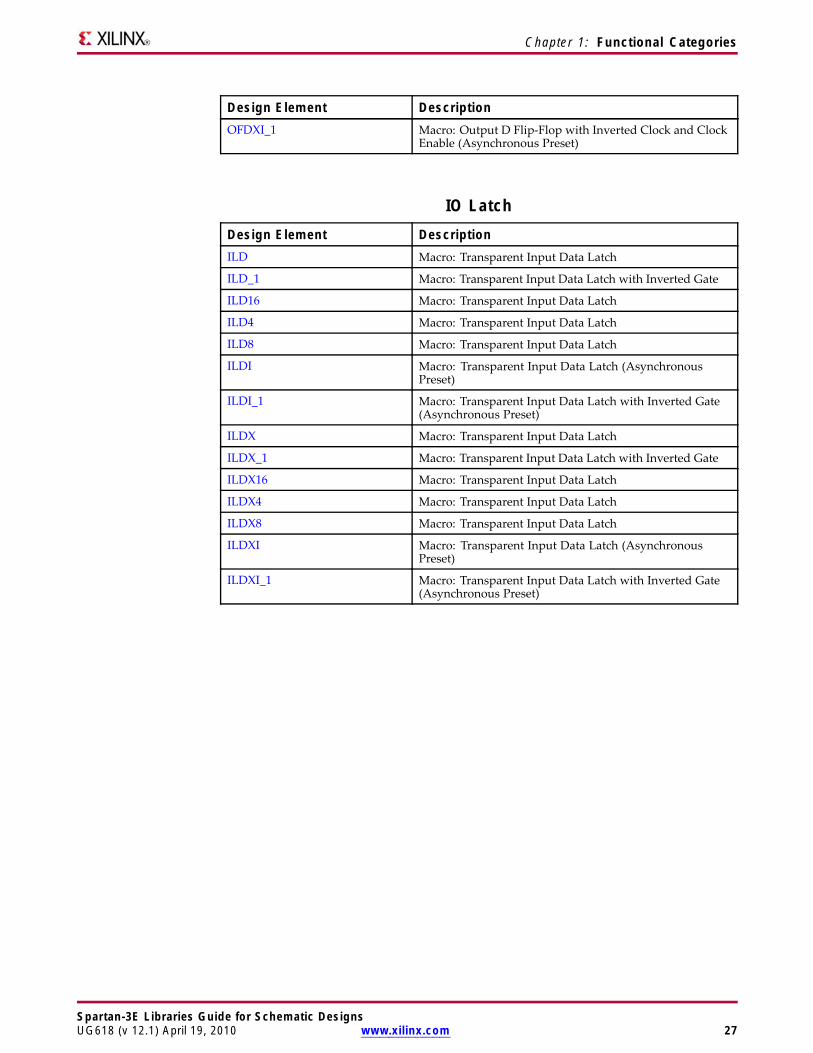
Chapter 1: Functional Categories
Design Element DescriptionOFDXI_1 Macro: Output D Flip-Flop with Inverted Clock and Clock
Enable (Asynchronous Preset)
IO LatchDesign Element DescriptionILD Macro: Transparent Input Data Latch
ILD_1 Macro: Transparent Input Data Latch with Inverted Gate
ILD16 Macro: Transparent Input Data Latch
ILD4 Macro: Transparent Input Data Latch
ILD8 Macro: Transparent Input Data Latch
ILDI Macro: Transparent Input Data Latch (AsynchronousPreset)
ILDI_1 Macro: Transparent Input Data Latch with Inverted Gate(Asynchronous Preset)
ILDX Macro: Transparent Input Data Latch
ILDX_1 Macro: Transparent Input Data Latch with Inverted Gate
ILDX16 Macro: Transparent Input Data Latch
ILDX4 Macro: Transparent Input Data Latch
ILDX8 Macro: Transparent Input Data Latch
ILDXI Macro: Transparent Input Data Latch (AsynchronousPreset)
ILDXI_1 Macro: Transparent Input Data Latch with Inverted Gate(Asynchronous Preset)
Spartan-3E Libraries Guide for Schematic DesignsUG618 (v 12.1) April 19, 2010 www.xilinx.com 27
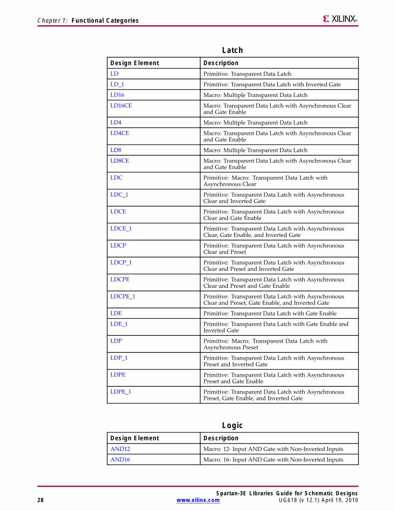
Chapter 1: Functional Categories
LatchDesign Element DescriptionLD Primitive: Transparent Data Latch
LD_1 Primitive: Transparent Data Latch with Inverted Gate
LD16 Macro: Multiple Transparent Data Latch
LD16CE Macro: Transparent Data Latch with Asynchronous Clearand Gate Enable
LD4 Macro: Multiple Transparent Data Latch
LD4CE Macro: Transparent Data Latch with Asynchronous Clearand Gate Enable
LD8 Macro: Multiple Transparent Data Latch
LD8CE Macro: Transparent Data Latch with Asynchronous Clearand Gate Enable
LDC Primitive: Macro: Transparent Data Latch withAsynchronous Clear
LDC_1 Primitive: Transparent Data Latch with AsynchronousClear and Inverted Gate
LDCE Primitive: Transparent Data Latch with AsynchronousClear and Gate Enable
LDCE_1 Primitive: Transparent Data Latch with AsynchronousClear, Gate Enable, and Inverted Gate
LDCP Primitive: Transparent Data Latch with AsynchronousClear and Preset
LDCP_1 Primitive: Transparent Data Latch with AsynchronousClear and Preset and Inverted Gate
LDCPE Primitive: Transparent Data Latch with AsynchronousClear and Preset and Gate Enable
LDCPE_1 Primitive: Transparent Data Latch with AsynchronousClear and Preset, Gate Enable, and Inverted Gate
LDE Primitive: Transparent Data Latch with Gate Enable
LDE_1 Primitive: Transparent Data Latch with Gate Enable andInverted Gate
LDP Primitive: Macro: Transparent Data Latch withAsynchronous Preset
LDP_1 Primitive: Transparent Data Latch with AsynchronousPreset and Inverted Gate
LDPE Primitive: Transparent Data Latch with AsynchronousPreset and Gate Enable
LDPE_1 Primitive: Transparent Data Latch with AsynchronousPreset, Gate Enable, and Inverted Gate
LogicDesign Element DescriptionAND12 Macro: 12- Input AND Gate with Non-Inverted Inputs
AND16 Macro: 16- Input AND Gate with Non-Inverted Inputs
Spartan-3E Libraries Guide for Schematic Designs28 www.xilinx.com UG618 (v 12.1) April 19, 2010
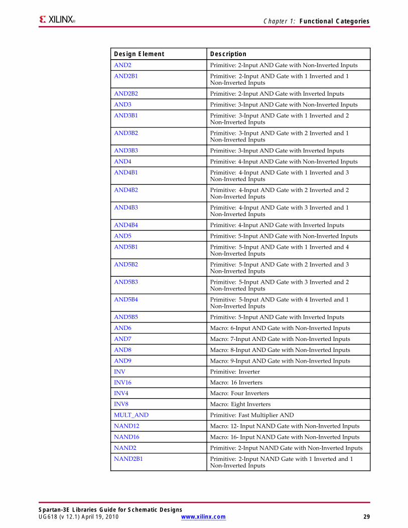
Chapter 1: Functional Categories
Design Element DescriptionAND2 Primitive: 2-Input AND Gate with Non-Inverted Inputs
AND2B1 Primitive: 2-Input AND Gate with 1 Inverted and 1Non-Inverted Inputs
AND2B2 Primitive: 2-Input AND Gate with Inverted Inputs
AND3 Primitive: 3-Input AND Gate with Non-Inverted Inputs
AND3B1 Primitive: 3-Input AND Gate with 1 Inverted and 2Non-Inverted Inputs
AND3B2 Primitive: 3-Input AND Gate with 2 Inverted and 1Non-Inverted Inputs
AND3B3 Primitive: 3-Input AND Gate with Inverted Inputs
AND4 Primitive: 4-Input AND Gate with Non-Inverted Inputs
AND4B1 Primitive: 4-Input AND Gate with 1 Inverted and 3Non-Inverted Inputs
AND4B2 Primitive: 4-Input AND Gate with 2 Inverted and 2Non-Inverted Inputs
AND4B3 Primitive: 4-Input AND Gate with 3 Inverted and 1Non-Inverted Inputs
AND4B4 Primitive: 4-Input AND Gate with Inverted Inputs
AND5 Primitive: 5-Input AND Gate with Non-Inverted Inputs
AND5B1 Primitive: 5-Input AND Gate with 1 Inverted and 4Non-Inverted Inputs
AND5B2 Primitive: 5-Input AND Gate with 2 Inverted and 3Non-Inverted Inputs
AND5B3 Primitive: 5-Input AND Gate with 3 Inverted and 2Non-Inverted Inputs
AND5B4 Primitive: 5-Input AND Gate with 4 Inverted and 1Non-Inverted Inputs
AND5B5 Primitive: 5-Input AND Gate with Inverted Inputs
AND6 Macro: 6-Input AND Gate with Non-Inverted Inputs
AND7 Macro: 7-Input AND Gate with Non-Inverted Inputs
AND8 Macro: 8-Input AND Gate with Non-Inverted Inputs
AND9 Macro: 9-Input AND Gate with Non-Inverted Inputs
INV Primitive: Inverter
INV16 Macro: 16 Inverters
INV4 Macro: Four Inverters
INV8 Macro: Eight Inverters
MULT_AND Primitive: Fast Multiplier AND
NAND12 Macro: 12- Input NAND Gate with Non-Inverted Inputs
NAND16 Macro: 16- Input NAND Gate with Non-Inverted Inputs
NAND2 Primitive: 2-Input NAND Gate with Non-Inverted Inputs
NAND2B1 Primitive: 2-Input NAND Gate with 1 Inverted and 1Non-Inverted Inputs
Spartan-3E Libraries Guide for Schematic DesignsUG618 (v 12.1) April 19, 2010 www.xilinx.com 29
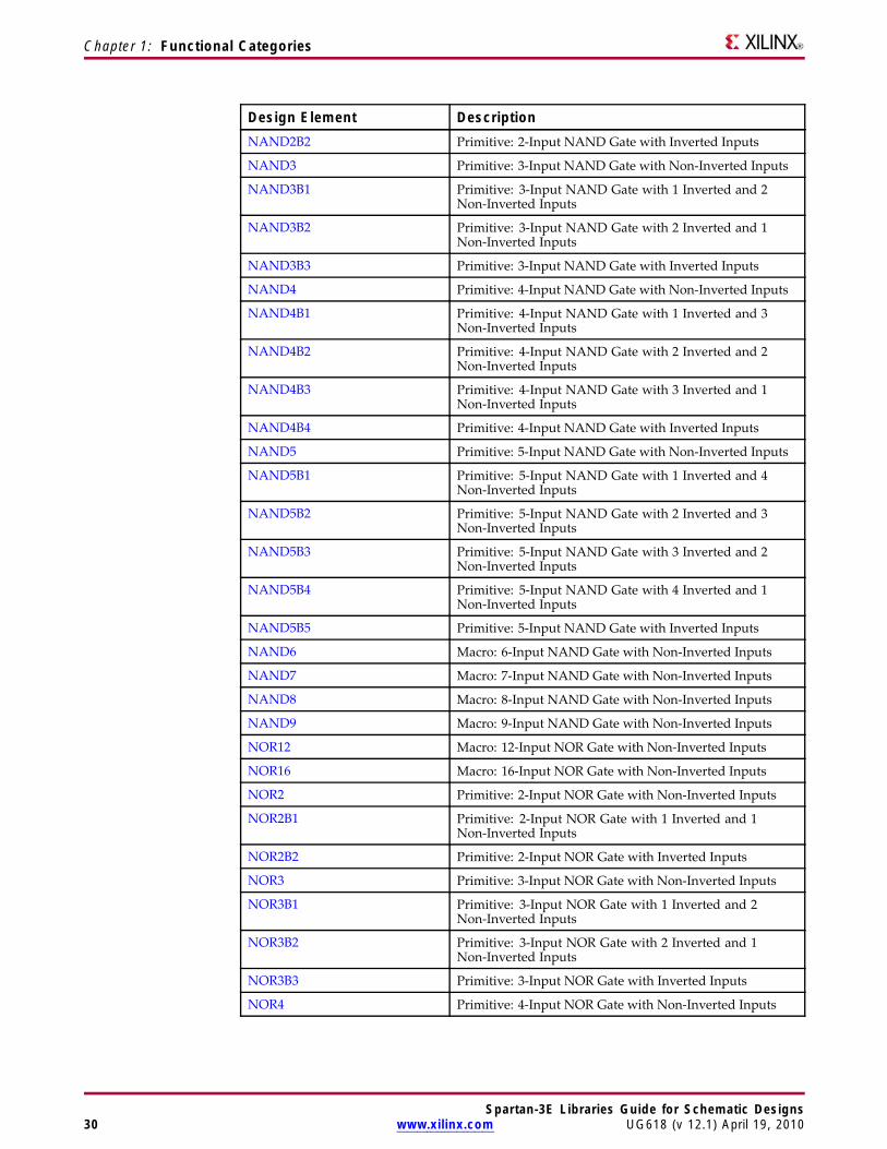
Chapter 1: Functional Categories
Design Element DescriptionNAND2B2 Primitive: 2-Input NAND Gate with Inverted Inputs
NAND3 Primitive: 3-Input NAND Gate with Non-Inverted Inputs
NAND3B1 Primitive: 3-Input NAND Gate with 1 Inverted and 2Non-Inverted Inputs
NAND3B2 Primitive: 3-Input NAND Gate with 2 Inverted and 1Non-Inverted Inputs
NAND3B3 Primitive: 3-Input NAND Gate with Inverted Inputs
NAND4 Primitive: 4-Input NAND Gate with Non-Inverted Inputs
NAND4B1 Primitive: 4-Input NAND Gate with 1 Inverted and 3Non-Inverted Inputs
NAND4B2 Primitive: 4-Input NAND Gate with 2 Inverted and 2Non-Inverted Inputs
NAND4B3 Primitive: 4-Input NAND Gate with 3 Inverted and 1Non-Inverted Inputs
NAND4B4 Primitive: 4-Input NAND Gate with Inverted Inputs
NAND5 Primitive: 5-Input NAND Gate with Non-Inverted Inputs
NAND5B1 Primitive: 5-Input NAND Gate with 1 Inverted and 4Non-Inverted Inputs
NAND5B2 Primitive: 5-Input NAND Gate with 2 Inverted and 3Non-Inverted Inputs
NAND5B3 Primitive: 5-Input NAND Gate with 3 Inverted and 2Non-Inverted Inputs
NAND5B4 Primitive: 5-Input NAND Gate with 4 Inverted and 1Non-Inverted Inputs
NAND5B5 Primitive: 5-Input NAND Gate with Inverted Inputs
NAND6 Macro: 6-Input NAND Gate with Non-Inverted Inputs
NAND7 Macro: 7-Input NAND Gate with Non-Inverted Inputs
NAND8 Macro: 8-Input NAND Gate with Non-Inverted Inputs
NAND9 Macro: 9-Input NAND Gate with Non-Inverted Inputs
NOR12 Macro: 12-Input NOR Gate with Non-Inverted Inputs
NOR16 Macro: 16-Input NOR Gate with Non-Inverted Inputs
NOR2 Primitive: 2-Input NOR Gate with Non-Inverted Inputs
NOR2B1 Primitive: 2-Input NOR Gate with 1 Inverted and 1Non-Inverted Inputs
NOR2B2 Primitive: 2-Input NOR Gate with Inverted Inputs
NOR3 Primitive: 3-Input NOR Gate with Non-Inverted Inputs
NOR3B1 Primitive: 3-Input NOR Gate with 1 Inverted and 2Non-Inverted Inputs
NOR3B2 Primitive: 3-Input NOR Gate with 2 Inverted and 1Non-Inverted Inputs
NOR3B3 Primitive: 3-Input NOR Gate with Inverted Inputs
NOR4 Primitive: 4-Input NOR Gate with Non-Inverted Inputs
Spartan-3E Libraries Guide for Schematic Designs30 www.xilinx.com UG618 (v 12.1) April 19, 2010
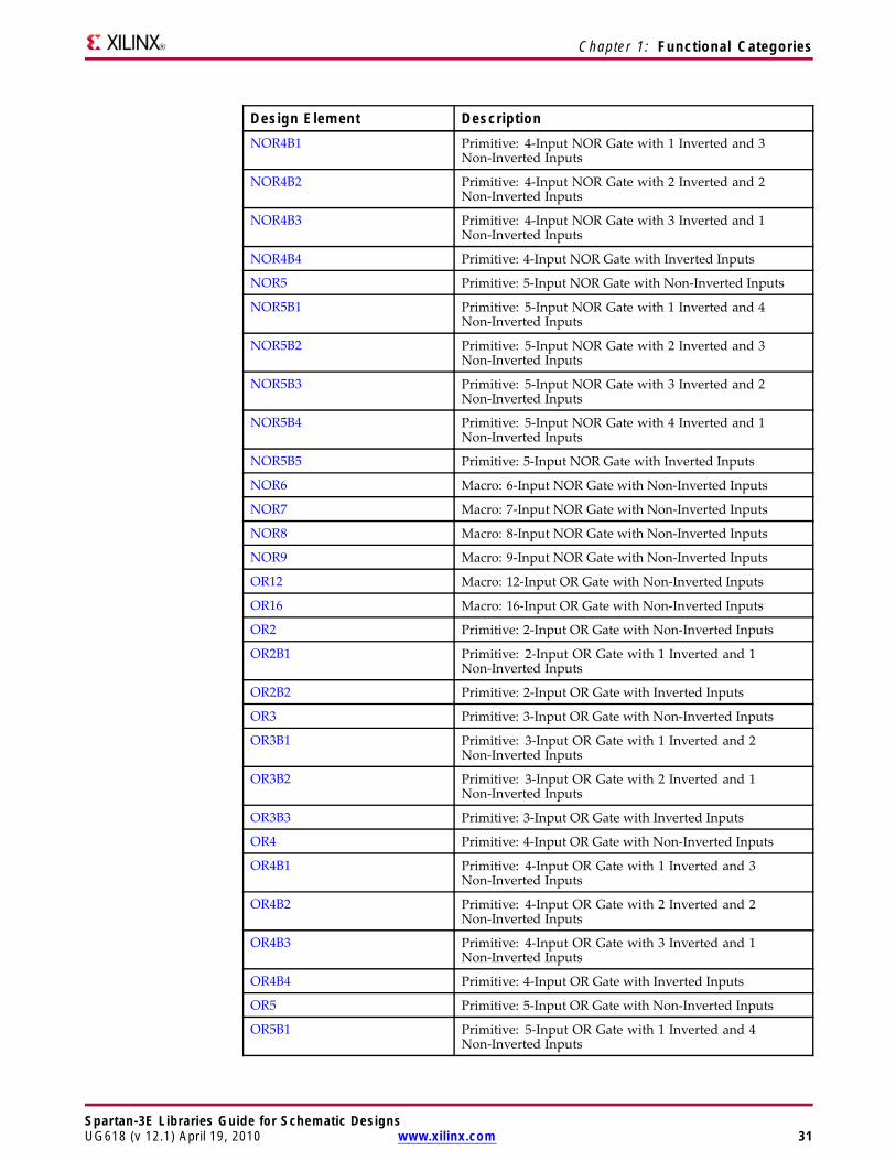
Chapter 1: Functional Categories
Design Element DescriptionNOR4B1 Primitive: 4-Input NOR Gate with 1 Inverted and 3
Non-Inverted Inputs
NOR4B2 Primitive: 4-Input NOR Gate with 2 Inverted and 2Non-Inverted Inputs
NOR4B3 Primitive: 4-Input NOR Gate with 3 Inverted and 1Non-Inverted Inputs
NOR4B4 Primitive: 4-Input NOR Gate with Inverted Inputs
NOR5 Primitive: 5-Input NOR Gate with Non-Inverted Inputs
NOR5B1 Primitive: 5-Input NOR Gate with 1 Inverted and 4Non-Inverted Inputs
NOR5B2 Primitive: 5-Input NOR Gate with 2 Inverted and 3Non-Inverted Inputs
NOR5B3 Primitive: 5-Input NOR Gate with 3 Inverted and 2Non-Inverted Inputs
NOR5B4 Primitive: 5-Input NOR Gate with 4 Inverted and 1Non-Inverted Inputs
NOR5B5 Primitive: 5-Input NOR Gate with Inverted Inputs
NOR6 Macro: 6-Input NOR Gate with Non-Inverted Inputs
NOR7 Macro: 7-Input NOR Gate with Non-Inverted Inputs
NOR8 Macro: 8-Input NOR Gate with Non-Inverted Inputs
NOR9 Macro: 9-Input NOR Gate with Non-Inverted Inputs
OR12 Macro: 12-Input OR Gate with Non-Inverted Inputs
OR16 Macro: 16-Input OR Gate with Non-Inverted Inputs
OR2 Primitive: 2-Input OR Gate with Non-Inverted Inputs
OR2B1 Primitive: 2-Input OR Gate with 1 Inverted and 1Non-Inverted Inputs
OR2B2 Primitive: 2-Input OR Gate with Inverted Inputs
OR3 Primitive: 3-Input OR Gate with Non-Inverted Inputs
OR3B1 Primitive: 3-Input OR Gate with 1 Inverted and 2Non-Inverted Inputs
OR3B2 Primitive: 3-Input OR Gate with 2 Inverted and 1Non-Inverted Inputs
OR3B3 Primitive: 3-Input OR Gate with Inverted Inputs
OR4 Primitive: 4-Input OR Gate with Non-Inverted Inputs
OR4B1 Primitive: 4-Input OR Gate with 1 Inverted and 3Non-Inverted Inputs
OR4B2 Primitive: 4-Input OR Gate with 2 Inverted and 2Non-Inverted Inputs
OR4B3 Primitive: 4-Input OR Gate with 3 Inverted and 1Non-Inverted Inputs
OR4B4 Primitive: 4-Input OR Gate with Inverted Inputs
OR5 Primitive: 5-Input OR Gate with Non-Inverted Inputs
OR5B1 Primitive: 5-Input OR Gate with 1 Inverted and 4Non-Inverted Inputs
Spartan-3E Libraries Guide for Schematic DesignsUG618 (v 12.1) April 19, 2010 www.xilinx.com 31
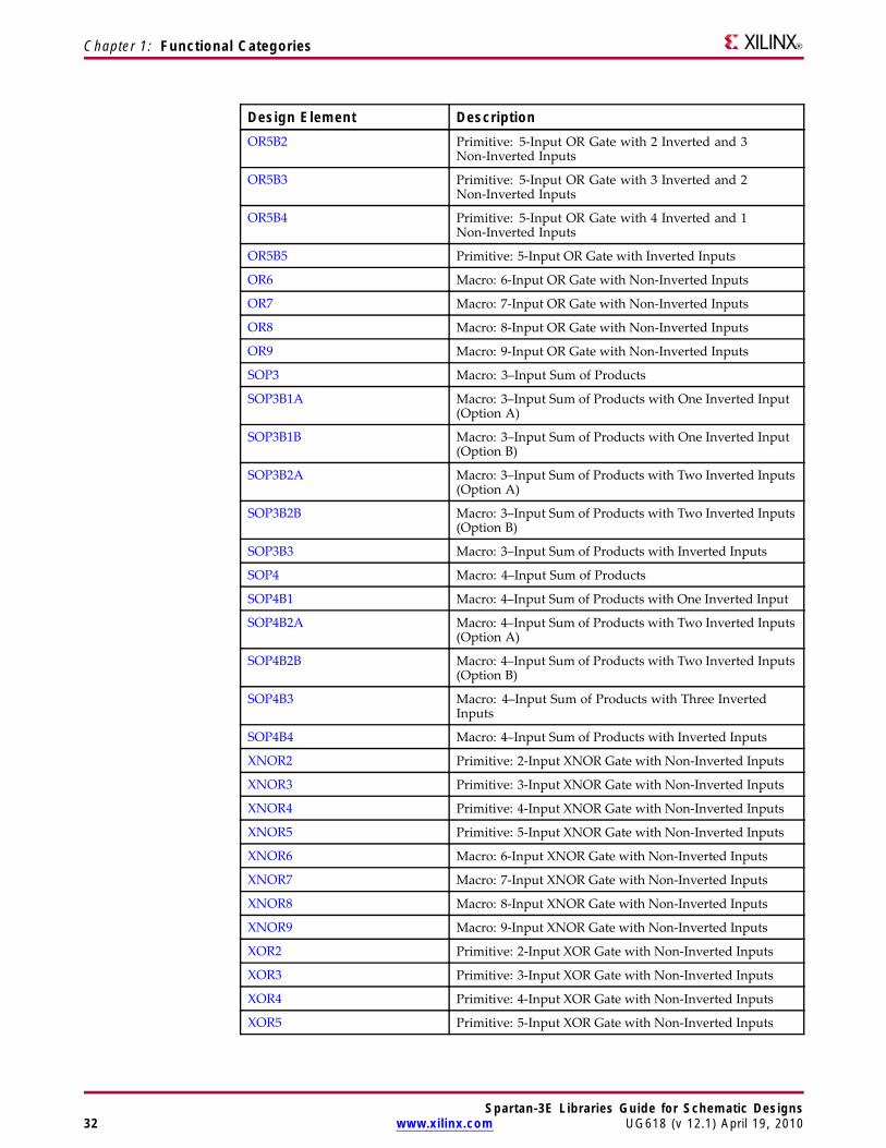
Chapter 1: Functional Categories
Design Element DescriptionOR5B2 Primitive: 5-Input OR Gate with 2 Inverted and 3
Non-Inverted Inputs
OR5B3 Primitive: 5-Input OR Gate with 3 Inverted and 2Non-Inverted Inputs
OR5B4 Primitive: 5-Input OR Gate with 4 Inverted and 1Non-Inverted Inputs
OR5B5 Primitive: 5-Input OR Gate with Inverted Inputs
OR6 Macro: 6-Input OR Gate with Non-Inverted Inputs
OR7 Macro: 7-Input OR Gate with Non-Inverted Inputs
OR8 Macro: 8-Input OR Gate with Non-Inverted Inputs
OR9 Macro: 9-Input OR Gate with Non-Inverted Inputs
SOP3 Macro: 3–Input Sum of Products
SOP3B1A Macro: 3–Input Sum of Products with One Inverted Input(Option A)
SOP3B1B Macro: 3–Input Sum of Products with One Inverted Input(Option B)
SOP3B2A Macro: 3–Input Sum of Products with Two Inverted Inputs(Option A)
SOP3B2B Macro: 3–Input Sum of Products with Two Inverted Inputs(Option B)
SOP3B3 Macro: 3–Input Sum of Products with Inverted Inputs
SOP4 Macro: 4–Input Sum of Products
SOP4B1 Macro: 4–Input Sum of Products with One Inverted Input
SOP4B2A Macro: 4–Input Sum of Products with Two Inverted Inputs(Option A)
SOP4B2B Macro: 4–Input Sum of Products with Two Inverted Inputs(Option B)
SOP4B3 Macro: 4–Input Sum of Products with Three InvertedInputs
SOP4B4 Macro: 4–Input Sum of Products with Inverted Inputs
XNOR2 Primitive: 2-Input XNOR Gate with Non-Inverted Inputs
XNOR3 Primitive: 3-Input XNOR Gate with Non-Inverted Inputs
XNOR4 Primitive: 4-Input XNOR Gate with Non-Inverted Inputs
XNOR5 Primitive: 5-Input XNOR Gate with Non-Inverted Inputs
XNOR6 Macro: 6-Input XNOR Gate with Non-Inverted Inputs
XNOR7 Macro: 7-Input XNOR Gate with Non-Inverted Inputs
XNOR8 Macro: 8-Input XNOR Gate with Non-Inverted Inputs
XNOR9 Macro: 9-Input XNOR Gate with Non-Inverted Inputs
XOR2 Primitive: 2-Input XOR Gate with Non-Inverted Inputs
XOR3 Primitive: 3-Input XOR Gate with Non-Inverted Inputs
XOR4 Primitive: 4-Input XOR Gate with Non-Inverted Inputs
XOR5 Primitive: 5-Input XOR Gate with Non-Inverted Inputs
Spartan-3E Libraries Guide for Schematic Designs32 www.xilinx.com UG618 (v 12.1) April 19, 2010
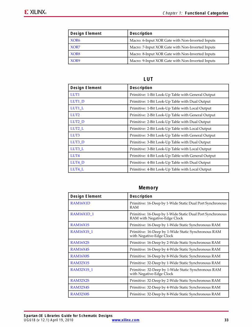
Chapter 1: Functional Categories
Design Element DescriptionXOR6 Macro: 6-Input XOR Gate with Non-Inverted Inputs
XOR7 Macro: 7-Input XOR Gate with Non-Inverted Inputs
XOR8 Macro: 8-Input XOR Gate with Non-Inverted Inputs
XOR9 Macro: 9-Input XOR Gate with Non-Inverted Inputs
LUTDesign Element DescriptionLUT1 Primitive: 1-Bit Look-Up Table with General Output
LUT1_D Primitive: 1-Bit Look-Up Table with Dual Output
LUT1_L Primitive: 1-Bit Look-Up Table with Local Output
LUT2 Primitive: 2-Bit Look-Up Table with General Output
LUT2_D Primitive: 2-Bit Look-Up Table with Dual Output
LUT2_L Primitive: 2-Bit Look-Up Table with Local Output
LUT3 Primitive: 3-Bit Look-Up Table with General Output
LUT3_D Primitive: 3-Bit Look-Up Table with Dual Output
LUT3_L Primitive: 3-Bit Look-Up Table with Local Output
LUT4 Primitive: 4-Bit Look-Up-Table with General Output
LUT4_D Primitive: 4-Bit Look-Up Table with Dual Output
LUT4_L Primitive: 4-Bit Look-Up Table with Local Output
MemoryDesign Element DescriptionRAM16X1D Primitive: 16-Deep by 1-Wide Static Dual Port Synchronous
RAM
RAM16X1D_1 Primitive: 16-Deep by 1-Wide Static Dual Port SynchronousRAM with Negative-Edge Clock
RAM16X1S Primitive: 16-Deep by 1-Wide Static Synchronous RAM
RAM16X1S_1 Primitive: 16-Deep by 1-Wide Static Synchronous RAMwith Negative-Edge Clock
RAM16X2S Primitive: 16-Deep by 2-Wide Static Synchronous RAM
RAM16X4S Primitive: 16-Deep by 4-Wide Static Synchronous RAM
RAM16X8S Primitive: 16-Deep by 8-Wide Static Synchronous RAM
RAM32X1S Primitive: 32-Deep by 1-Wide Static Synchronous RAM
RAM32X1S_1 Primitive: 32-Deep by 1-Wide Static Synchronous RAMwith Negative-Edge Clock
RAM32X2S Primitive: 32-Deep by 2-Wide Static Synchronous RAM
RAM32X4S Primitive: 32-Deep by 4-Wide Static Synchronous RAM
RAM32X8S Primitive: 32-Deep by 8-Wide Static Synchronous RAM
Spartan-3E Libraries Guide for Schematic DesignsUG618 (v 12.1) April 19, 2010 www.xilinx.com 33
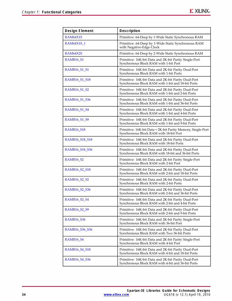
Chapter 1: Functional Categories
Design Element DescriptionRAM64X1S Primitive: 64-Deep by 1-Wide Static Synchronous RAM
RAM64X1S_1 Primitive: 64-Deep by 1-Wide Static Synchronous RAMwith Negative-Edge Clock
RAM64X2S Primitive: 64-Deep by 2-Wide Static Synchronous RAM
RAMB16_S1 Primitive: 16K-bit Data and 2K-bit Parity Single-PortSynchronous Block RAM with 1-bit Port
RAMB16_S1_S1 Primitive: 16K-bit Data and 2K-bit Parity Dual-PortSynchronous Block RAM with 1-bit Ports
RAMB16_S1_S18 Primitive: 16K-bit Data and 2K-bit Parity Dual-PortSynchronous Block RAM with 1-bit and 18-bit Ports
RAMB16_S1_S2 Primitive: 16K-bit Data and 2K-bit Parity Dual-PortSynchronous Block RAM with 1-bit and 2-bit Ports
RAMB16_S1_S36 Primitive: 16K-bit Data and 2K-bit Parity Dual-PortSynchronous Block RAM with 1-bit and 36-bit Ports
RAMB16_S1_S4 Primitive: 16K-bit Data and 2K-bit Parity Dual-PortSynchronous Block RAM with 1-bit and 4-bit Ports
RAMB16_S1_S9 Primitive: 16K-bit Data and 2K-bit Parity Dual-PortSynchronous Block RAM with 1-bit and 9-bit Ports
RAMB16_S18 Primitive: 16K-bit Data + 2K-bit Parity Memory, Single-PortSynchronous Block RAM with 18-bit Port
RAMB16_S18_S18 Primitive: 16K-bit Data and 2K-bit Parity Dual-PortSynchronous Block RAM with 18-bit Ports
RAMB16_S18_S36 Primitive: 16K-bit Data and 2K-bit Parity Dual-PortSynchronous Block RAM with 18-bit and 36-bit Ports
RAMB16_S2 Primitive: 16K-bit Data and 2K-bit Parity Single-PortSynchronous Block RAM with 2-bit Port
RAMB16_S2_S18 Primitive: 16K-bit Data and 2K-bit Parity Dual-PortSynchronous Block RAM with 2-bit and 18-bit Ports
RAMB16_S2_S2 Primitive: 16K-bit Data and 2K-bit Parity Dual-PortSynchronous Block RAM with 2-bit Ports
RAMB16_S2_S36 Primitive: 16K-bit Data and 2K-bit Parity Dual-PortSynchronous Block RAM with 2-bit and 36-bit Ports
RAMB16_S2_S4 Primitive: 16K-bit Data and 2K-bit Parity Dual-PortSynchronous Block RAM with 2-bit and 4-bit Ports
RAMB16_S2_S9 Primitive: 16K-bit Data and 2K-bit Parity Dual-PortSynchronous Block RAM with 2-bit and 9-bit Ports
RAMB16_S36 Primitive: 16K-bit Data and 2K-bit Parity Single-PortSynchronous Block RAM with 36-bit Port
RAMB16_S36_S36 Primitive: 16K-bit Data and 2K-bit Parity Dual-PortSynchronous Block RAM with Two 36-bit Ports
RAMB16_S4 Primitive: 16K-bit Data and 2K-bit Parity Single-PortSynchronous Block RAM with 4-bit Port
RAMB16_S4_S18 Primitive: 16K-bit Data and 2K-bit Parity Dual-PortSynchronous Block RAM with 4-bit and 18-bit Ports
RAMB16_S4_S36 Primitive: 16K-bit Data and 2K-bit Parity Dual-PortSynchronous Block RAM with 4-bit and 36-bit Ports
Spartan-3E Libraries Guide for Schematic Designs34 www.xilinx.com UG618 (v 12.1) April 19, 2010
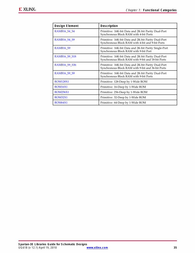
Chapter 1: Functional Categories
Design Element DescriptionRAMB16_S4_S4 Primitive: 16K-bit Data and 2K-bit Parity Dual-Port
Synchronous Block RAM with 4-bit Ports
RAMB16_S4_S9 Primitive: 16K-bit Data and 2K-bit Parity Dual-PortSynchronous Block RAM with 4-bit and 9-bit Ports
RAMB16_S9 Primitive: 16K-bit Data and 2K-bit Parity Single-PortSynchronous Block RAM with 9-bit Port
RAMB16_S9_S18 Primitive: 16K-bit Data and 2K-bit Parity Dual-PortSynchronous Block RAM with 9-bit and 18-bit Ports
RAMB16_S9_S36 Primitive: 16K-bit Data and 2K-bit Parity Dual-PortSynchronous Block RAM with 9-bit and 36-bit Ports
RAMB16_S9_S9 Primitive: 16K-bit Data and 2K-bit Parity Dual-PortSynchronous Block RAM with 9-bit Ports
ROM128X1 Primitive: 128-Deep by 1-Wide ROM
ROM16X1 Primitive: 16-Deep by 1-Wide ROM
ROM256X1 Primitive: 256-Deep by 1-Wide ROM
ROM32X1 Primitive: 32-Deep by 1-Wide ROM
ROM64X1 Primitive: 64-Deep by 1-Wide ROM
Spartan-3E Libraries Guide for Schematic DesignsUG618 (v 12.1) April 19, 2010 www.xilinx.com 35
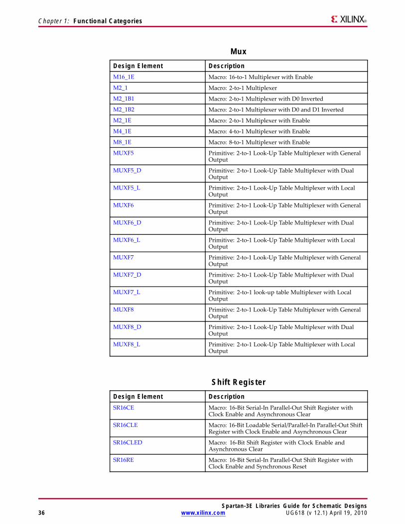
Chapter 1: Functional Categories
MuxDesign Element DescriptionM16_1E Macro: 16-to-1 Multiplexer with Enable
M2_1 Macro: 2-to-1 Multiplexer
M2_1B1 Macro: 2-to-1 Multiplexer with D0 Inverted
M2_1B2 Macro: 2-to-1 Multiplexer with D0 and D1 Inverted
M2_1E Macro: 2-to-1 Multiplexer with Enable
M4_1E Macro: 4-to-1 Multiplexer with Enable
M8_1E Macro: 8-to-1 Multiplexer with Enable
MUXF5 Primitive: 2-to-1 Look-Up Table Multiplexer with GeneralOutput
MUXF5_D Primitive: 2-to-1 Look-Up Table Multiplexer with DualOutput
MUXF5_L Primitive: 2-to-1 Look-Up Table Multiplexer with LocalOutput
MUXF6 Primitive: 2-to-1 Look-Up Table Multiplexer with GeneralOutput
MUXF6_D Primitive: 2-to-1 Look-Up Table Multiplexer with DualOutput
MUXF6_L Primitive: 2-to-1 Look-Up Table Multiplexer with LocalOutput
MUXF7 Primitive: 2-to-1 Look-Up Table Multiplexer with GeneralOutput
MUXF7_D Primitive: 2-to-1 Look-Up Table Multiplexer with DualOutput
MUXF7_L Primitive: 2-to-1 look-up table Multiplexer with LocalOutput
MUXF8 Primitive: 2-to-1 Look-Up Table Multiplexer with GeneralOutput
MUXF8_D Primitive: 2-to-1 Look-Up Table Multiplexer with DualOutput
MUXF8_L Primitive: 2-to-1 Look-Up Table Multiplexer with LocalOutput
Shift RegisterDesign Element DescriptionSR16CE Macro: 16-Bit Serial-In Parallel-Out Shift Register with
Clock Enable and Asynchronous Clear
SR16CLE Macro: 16-Bit Loadable Serial/Parallel-In Parallel-Out ShiftRegister with Clock Enable and Asynchronous Clear
SR16CLED Macro: 16-Bit Shift Register with Clock Enable andAsynchronous Clear
SR16RE Macro: 16-Bit Serial-In Parallel-Out Shift Register withClock Enable and Synchronous Reset
Spartan-3E Libraries Guide for Schematic Designs36 www.xilinx.com UG618 (v 12.1) April 19, 2010
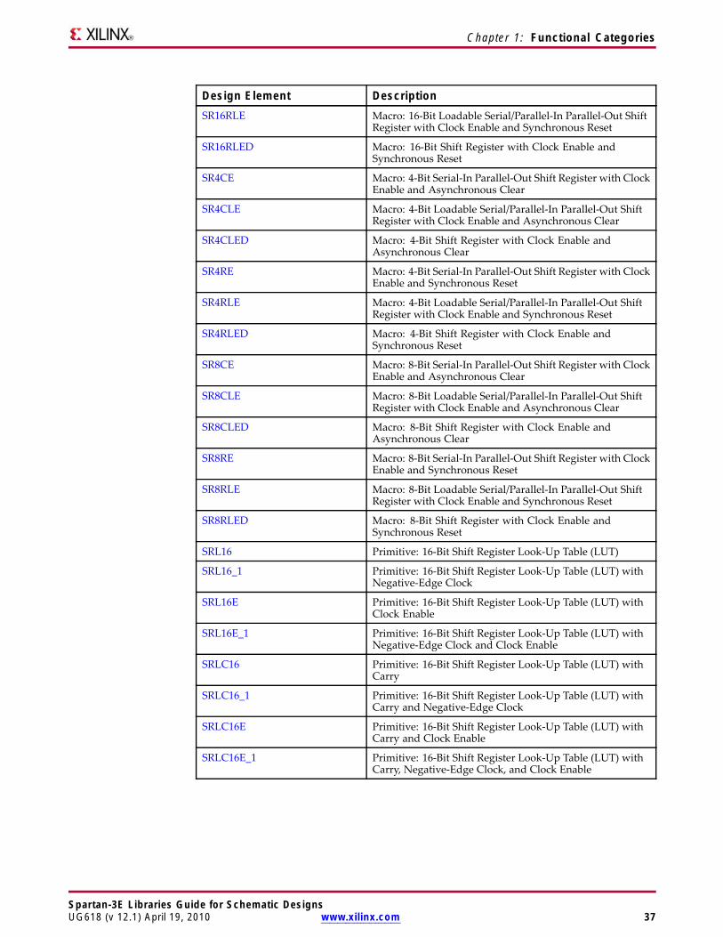
Chapter 1: Functional Categories
Design Element DescriptionSR16RLE Macro: 16-Bit Loadable Serial/Parallel-In Parallel-Out Shift
Register with Clock Enable and Synchronous Reset
SR16RLED Macro: 16-Bit Shift Register with Clock Enable andSynchronous Reset
SR4CE Macro: 4-Bit Serial-In Parallel-Out Shift Register with ClockEnable and Asynchronous Clear
SR4CLE Macro: 4-Bit Loadable Serial/Parallel-In Parallel-Out ShiftRegister with Clock Enable and Asynchronous Clear
SR4CLED Macro: 4-Bit Shift Register with Clock Enable andAsynchronous Clear
SR4RE Macro: 4-Bit Serial-In Parallel-Out Shift Register with ClockEnable and Synchronous Reset
SR4RLE Macro: 4-Bit Loadable Serial/Parallel-In Parallel-Out ShiftRegister with Clock Enable and Synchronous Reset
SR4RLED Macro: 4-Bit Shift Register with Clock Enable andSynchronous Reset
SR8CE Macro: 8-Bit Serial-In Parallel-Out Shift Register with ClockEnable and Asynchronous Clear
SR8CLE Macro: 8-Bit Loadable Serial/Parallel-In Parallel-Out ShiftRegister with Clock Enable and Asynchronous Clear
SR8CLED Macro: 8-Bit Shift Register with Clock Enable andAsynchronous Clear
SR8RE Macro: 8-Bit Serial-In Parallel-Out Shift Register with ClockEnable and Synchronous Reset
SR8RLE Macro: 8-Bit Loadable Serial/Parallel-In Parallel-Out ShiftRegister with Clock Enable and Synchronous Reset
SR8RLED Macro: 8-Bit Shift Register with Clock Enable andSynchronous Reset
SRL16 Primitive: 16-Bit Shift Register Look-Up Table (LUT)
SRL16_1 Primitive: 16-Bit Shift Register Look-Up Table (LUT) withNegative-Edge Clock
SRL16E Primitive: 16-Bit Shift Register Look-Up Table (LUT) withClock Enable
SRL16E_1 Primitive: 16-Bit Shift Register Look-Up Table (LUT) withNegative-Edge Clock and Clock Enable
SRLC16 Primitive: 16-Bit Shift Register Look-Up Table (LUT) withCarry
SRLC16_1 Primitive: 16-Bit Shift Register Look-Up Table (LUT) withCarry and Negative-Edge Clock
SRLC16E Primitive: 16-Bit Shift Register Look-Up Table (LUT) withCarry and Clock Enable
SRLC16E_1 Primitive: 16-Bit Shift Register Look-Up Table (LUT) withCarry, Negative-Edge Clock, and Clock Enable
Spartan-3E Libraries Guide for Schematic DesignsUG618 (v 12.1) April 19, 2010 www.xilinx.com 37
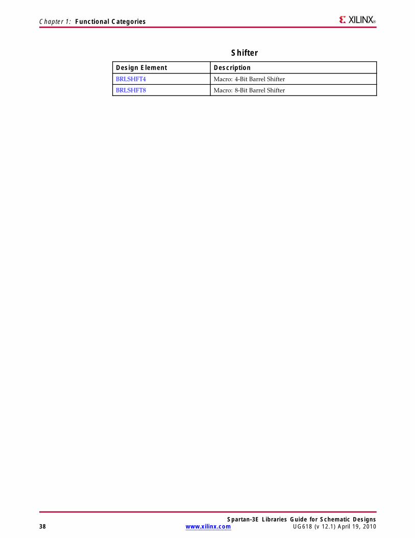
Chapter 1: Functional Categories
ShifterDesign Element DescriptionBRLSHFT4 Macro: 4-Bit Barrel Shifter
BRLSHFT8 Macro: 8-Bit Barrel Shifter
Spartan-3E Libraries Guide for Schematic Designs38 www.xilinx.com UG618 (v 12.1) April 19, 2010
Chapter 2
About Design ElementsThis section describes the design elements that can be used with this architecture. Thedesign elements are organized alphabetically.
The following information is provided for each design element, where applicable:
• Name of element
• Brief description
• Schematic symbol (if any)
• Logic Table (if any)
• Port Descriptions (if any)
• Design Entry Method
• Available Attributes (if any)
• For more information
You can find examples of VHDL and Verilog instantiation code in the ISE software (inthe main menu, select Edit > Language Templates or in the Libraries Guide for HDLDesigns for this architecture.
Spartan-3E Libraries Guide for Schematic DesignsUG618 (v 12.1) April 19, 2010 www.xilinx.com 39
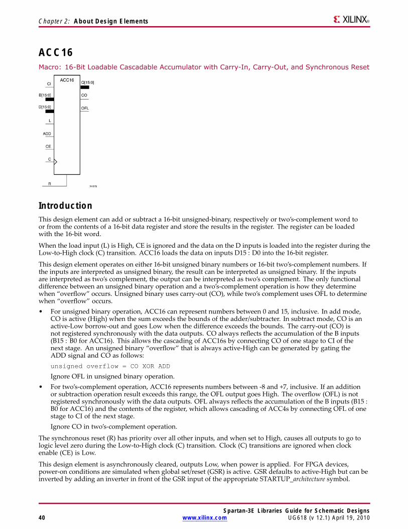
Chapter 2: About Design Elements
ACC16Macro: 16-Bit Loadable Cascadable Accumulator with Carry-In, Carry-Out, and Synchronous Reset
IntroductionThis design element can add or subtract a 16-bit unsigned-binary, respectively or two’s-complement word toor from the contents of a 16-bit data register and store the results in the register. The register can be loadedwith the 16-bit word.
When the load input (L) is High, CE is ignored and the data on the D inputs is loaded into the register during theLow-to-High clock (C) transition. ACC16 loads the data on inputs D15 : D0 into the 16-bit register.
This design element operates on either 16-bit unsigned binary numbers or 16-bit two’s-complement numbers. Ifthe inputs are interpreted as unsigned binary, the result can be interpreted as unsigned binary. If the inputsare interpreted as two’s complement, the output can be interpreted as two’s complement. The only functionaldifference between an unsigned binary operation and a two’s-complement operation is how they determinewhen “overflow” occurs. Unsigned binary uses carry-out (CO), while two’s complement uses OFL to determinewhen “overflow” occurs.• For unsigned binary operation, ACC16 can represent numbers between 0 and 15, inclusive. In add mode,
CO is active (High) when the sum exceeds the bounds of the adder/subtracter. In subtract mode, CO is anactive-Low borrow-out and goes Low when the difference exceeds the bounds. The carry-out (CO) isnot registered synchronously with the data outputs. CO always reflects the accumulation of the B inputs(B15 : B0 for ACC16). This allows the cascading of ACC16s by connecting CO of one stage to CI of thenext stage. An unsigned binary “overflow” that is always active-High can be generated by gating theADD signal and CO as follows:unsigned overflow = CO XOR ADD
Ignore OFL in unsigned binary operation.• For two’s-complement operation, ACC16 represents numbers between -8 and +7, inclusive. If an addition
or subtraction operation result exceeds this range, the OFL output goes High. The overflow (OFL) is notregistered synchronously with the data outputs. OFL always reflects the accumulation of the B inputs (B15 :B0 for ACC16) and the contents of the register, which allows cascading of ACC4s by connecting OFL of onestage to CI of the next stage.Ignore CO in two’s-complement operation.
The synchronous reset (R) has priority over all other inputs, and when set to High, causes all outputs to go tologic level zero during the Low-to-High clock (C) transition. Clock (C) transitions are ignored when clockenable (CE) is Low.
This design element is asynchronously cleared, outputs Low, when power is applied. For FPGA devices,power-on conditions are simulated when global set/reset (GSR) is active. GSR defaults to active-High but can beinverted by adding an inverter in front of the GSR input of the appropriate STARTUP_architecture symbol.
Spartan-3E Libraries Guide for Schematic Designs40 www.xilinx.com UG618 (v 12.1) April 19, 2010
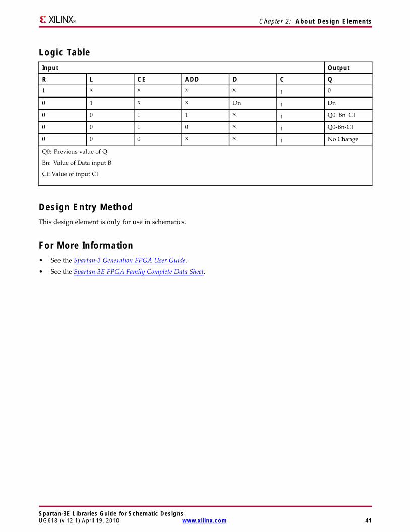
Chapter 2: About Design Elements
Logic TableInput Output
R L CE ADD D C Q1 x x x x ↑ 0
0 1 x x Dn ↑ Dn
0 0 1 1 x ↑ Q0+Bn+CI
0 0 1 0 x ↑ Q0-Bn-CI
0 0 0 x x ↑ No Change
Q0: Previous value of Q
Bn: Value of Data input B
CI: Value of input CI
Design Entry MethodThis design element is only for use in schematics.
For More Information• See the Spartan-3 Generation FPGA User Guide.
• See the Spartan-3E FPGA Family Complete Data Sheet.
Spartan-3E Libraries Guide for Schematic DesignsUG618 (v 12.1) April 19, 2010 www.xilinx.com 41
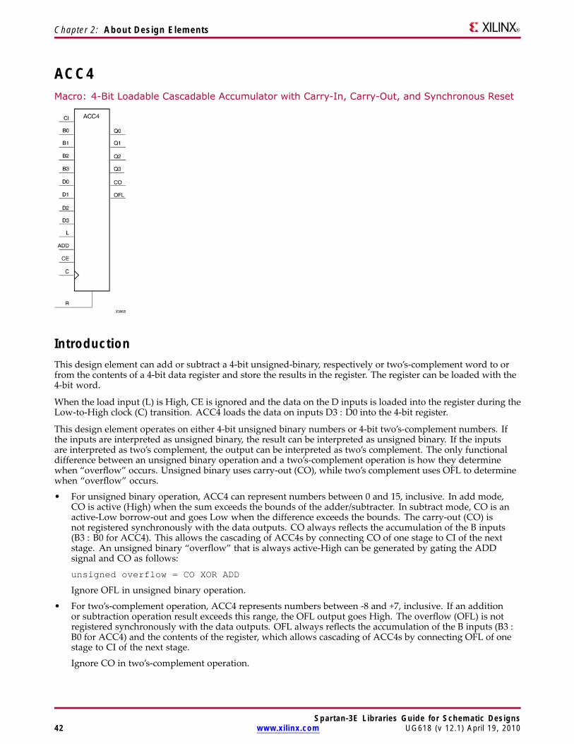
Chapter 2: About Design Elements
ACC4Macro: 4-Bit Loadable Cascadable Accumulator with Carry-In, Carry-Out, and Synchronous Reset
IntroductionThis design element can add or subtract a 4-bit unsigned-binary, respectively or two’s-complement word to orfrom the contents of a 4-bit data register and store the results in the register. The register can be loaded with the4-bit word.
When the load input (L) is High, CE is ignored and the data on the D inputs is loaded into the register during theLow-to-High clock (C) transition. ACC4 loads the data on inputs D3 : D0 into the 4-bit register.
This design element operates on either 4-bit unsigned binary numbers or 4-bit two’s-complement numbers. Ifthe inputs are interpreted as unsigned binary, the result can be interpreted as unsigned binary. If the inputsare interpreted as two’s complement, the output can be interpreted as two’s complement. The only functionaldifference between an unsigned binary operation and a two’s-complement operation is how they determinewhen “overflow” occurs. Unsigned binary uses carry-out (CO), while two’s complement uses OFL to determinewhen “overflow” occurs.
• For unsigned binary operation, ACC4 can represent numbers between 0 and 15, inclusive. In add mode,CO is active (High) when the sum exceeds the bounds of the adder/subtracter. In subtract mode, CO is anactive-Low borrow-out and goes Low when the difference exceeds the bounds. The carry-out (CO) isnot registered synchronously with the data outputs. CO always reflects the accumulation of the B inputs(B3 : B0 for ACC4). This allows the cascading of ACC4s by connecting CO of one stage to CI of the nextstage. An unsigned binary “overflow” that is always active-High can be generated by gating the ADDsignal and CO as follows:
unsigned overflow = CO XOR ADD
Ignore OFL in unsigned binary operation.
• For two’s-complement operation, ACC4 represents numbers between -8 and +7, inclusive. If an additionor subtraction operation result exceeds this range, the OFL output goes High. The overflow (OFL) is notregistered synchronously with the data outputs. OFL always reflects the accumulation of the B inputs (B3 :B0 for ACC4) and the contents of the register, which allows cascading of ACC4s by connecting OFL of onestage to CI of the next stage.
Ignore CO in two’s-complement operation.
Spartan-3E Libraries Guide for Schematic Designs42 www.xilinx.com UG618 (v 12.1) April 19, 2010
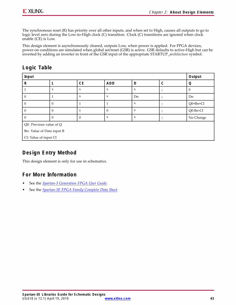
Chapter 2: About Design Elements
The synchronous reset (R) has priority over all other inputs, and when set to High, causes all outputs to go tologic level zero during the Low-to-High clock (C) transition. Clock (C) transitions are ignored when clockenable (CE) is Low.
This design element is asynchronously cleared, outputs Low, when power is applied. For FPGA devices,power-on conditions are simulated when global set/reset (GSR) is active. GSR defaults to active-High but can beinverted by adding an inverter in front of the GSR input of the appropriate STARTUP_architecture symbol.
Logic TableInput Output
R L CE ADD D C Q1 x x x x ↑ 0
0 1 x x Dn ↑ Dn
0 0 1 1 x ↑ Q0+Bn+CI
0 0 1 0 x ↑ Q0-Bn-CI
0 0 0 x x ↑ No Change
Q0: Previous value of Q
Bn: Value of Data input B
CI: Value of input CI
Design Entry MethodThis design element is only for use in schematics.
For More Information• See the Spartan-3 Generation FPGA User Guide.
• See the Spartan-3E FPGA Family Complete Data Sheet.
Spartan-3E Libraries Guide for Schematic DesignsUG618 (v 12.1) April 19, 2010 www.xilinx.com 43

Chapter 2: About Design Elements
ACC8Macro: 8-Bit Loadable Cascadable Accumulator with Carry-In, Carry-Out, and Synchronous Reset
IntroductionThis design element can add or subtract a 8-bit unsigned-binary, respectively or two’s-complement word to orfrom the contents of a 8-bit data register and store the results in the register. The register can be loaded with the8-bit word.
When the load input (L) is High, CE is ignored and the data on the D inputs is loaded into the register during theLow-to-High clock (C) transition. ACC8 loads the data on inputs D7 : D0 into the 8-bit register.
This design element operates on either 8-bit unsigned binary numbers or 8-bit two’s-complement numbers. Ifthe inputs are interpreted as unsigned binary, the result can be interpreted as unsigned binary. If the inputsare interpreted as two’s complement, the output can be interpreted as two’s complement. The only functionaldifference between an unsigned binary operation and a two’s-complement operation is how they determinewhen “overflow” occurs. Unsigned binary uses carry-out (CO), while two’s complement uses OFL to determinewhen “overflow” occurs.• For unsigned binary operation, ACC8 can represent numbers between 0 and 255, inclusive. In add mode,
CO is active (High) when the sum exceeds the bounds of the adder/subtracter. In subtract mode, CO is anactive-Low borrow-out and goes Low when the difference exceeds the bounds. The carry-out (CO) isnot registered synchronously with the data outputs. CO always reflects the accumulation of the B inputs(B3 : B0 for ACC4). This allows the cascading of ACC8s by connecting CO of one stage to CI of the nextstage. An unsigned binary “overflow” that is always active-High can be generated by gating the ADDsignal and CO as follows:unsigned overflow = CO XOR ADD
Ignore OFL in unsigned binary operation.• For two’s-complement operation, ACC8 represents numbers between -128 and +127, inclusive. If an addition
or subtraction operation result exceeds this range, the OFL output goes High. The overflow (OFL) is notregistered synchronously with the data outputs. OFL always reflects the accumulation of the B inputs (B3 :B0 for ACC8) and the contents of the register, which allows cascading of ACC8s by connecting OFL of onestage to CI of the next stage.Ignore CO in two’s-complement operation.
The synchronous reset (R) has priority over all other inputs, and when set to High, causes all outputs to go tologic level zero during the Low-to-High clock (C) transition. Clock (C) transitions are ignored when clockenable (CE) is Low.
This design element is asynchronously cleared, outputs Low, when power is applied. For FPGA devices,power-on conditions are simulated when global set/reset (GSR) is active. GSR defaults to active-High but can beinverted by adding an inverter in front of the GSR input of the appropriate STARTUP_architecture symbol.
Spartan-3E Libraries Guide for Schematic Designs44 www.xilinx.com UG618 (v 12.1) April 19, 2010
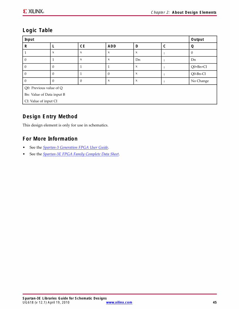
Chapter 2: About Design Elements
Logic TableInput Output
R L CE ADD D C Q1 x x x x ↑ 0
0 1 x x Dn ↑ Dn
0 0 1 1 x ↑ Q0+Bn+CI
0 0 1 0 x ↑ Q0-Bn-CI
0 0 0 x x ↑ No Change
Q0: Previous value of Q
Bn: Value of Data input B
CI: Value of input CI
Design Entry MethodThis design element is only for use in schematics.
For More Information• See the Spartan-3 Generation FPGA User Guide.
• See the Spartan-3E FPGA Family Complete Data Sheet.
Spartan-3E Libraries Guide for Schematic DesignsUG618 (v 12.1) April 19, 2010 www.xilinx.com 45
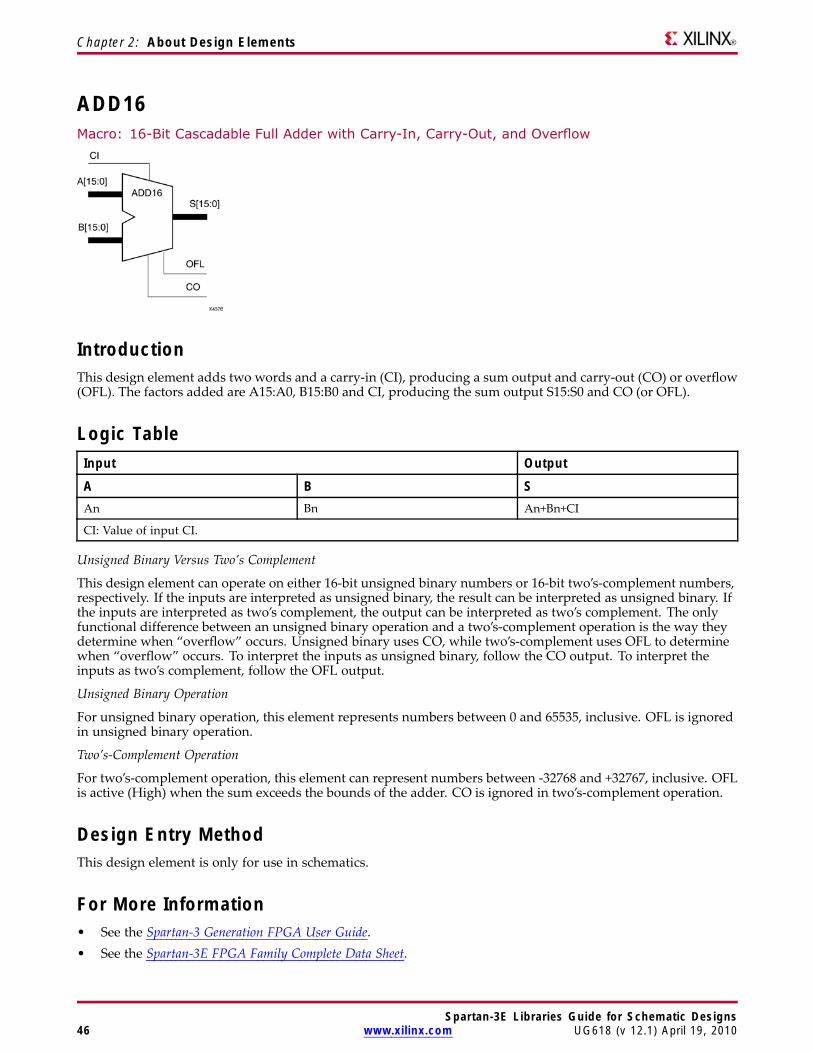
Chapter 2: About Design Elements
ADD16Macro: 16-Bit Cascadable Full Adder with Carry-In, Carry-Out, and Overflow
IntroductionThis design element adds two words and a carry-in (CI), producing a sum output and carry-out (CO) or overflow(OFL). The factors added are A15:A0, B15:B0 and CI, producing the sum output S15:S0 and CO (or OFL).
Logic TableInput Output
A B SAn Bn An+Bn+CI
CI: Value of input CI.
Unsigned Binary Versus Two’s Complement
This design element can operate on either 16-bit unsigned binary numbers or 16-bit two’s-complement numbers,respectively. If the inputs are interpreted as unsigned binary, the result can be interpreted as unsigned binary. Ifthe inputs are interpreted as two’s complement, the output can be interpreted as two’s complement. The onlyfunctional difference between an unsigned binary operation and a two’s-complement operation is the way theydetermine when “overflow” occurs. Unsigned binary uses CO, while two’s-complement uses OFL to determinewhen “overflow” occurs. To interpret the inputs as unsigned binary, follow the CO output. To interpret theinputs as two’s complement, follow the OFL output.
Unsigned Binary Operation
For unsigned binary operation, this element represents numbers between 0 and 65535, inclusive. OFL is ignoredin unsigned binary operation.
Two’s-Complement Operation
For two’s-complement operation, this element can represent numbers between -32768 and +32767, inclusive. OFLis active (High) when the sum exceeds the bounds of the adder. CO is ignored in two’s-complement operation.
Design Entry MethodThis design element is only for use in schematics.
For More Information• See the Spartan-3 Generation FPGA User Guide.• See the Spartan-3E FPGA Family Complete Data Sheet.
Spartan-3E Libraries Guide for Schematic Designs46 www.xilinx.com UG618 (v 12.1) April 19, 2010
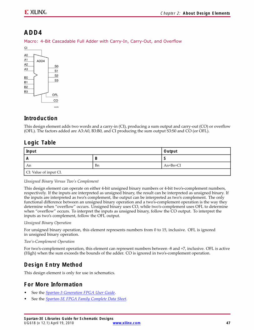
Chapter 2: About Design Elements
ADD4Macro: 4-Bit Cascadable Full Adder with Carry-In, Carry-Out, and Overflow
IntroductionThis design element adds two words and a carry-in (CI), producing a sum output and carry-out (CO) or overflow(OFL). The factors added are A3:A0, B3:B0, and CI producing the sum output S3:S0 and CO (or OFL).
Logic TableInput Output
A B SAn Bn An+Bn+CI
CI: Value of input CI.
Unsigned Binary Versus Two’s Complement
This design element can operate on either 4-bit unsigned binary numbers or 4-bit two’s-complement numbers,respectively. If the inputs are interpreted as unsigned binary, the result can be interpreted as unsigned binary. Ifthe inputs are interpreted as two’s complement, the output can be interpreted as two’s complement. The onlyfunctional difference between an unsigned binary operation and a two’s-complement operation is the way theydetermine when “overflow” occurs. Unsigned binary uses CO, while two’s-complement uses OFL to determinewhen “overflow” occurs. To interpret the inputs as unsigned binary, follow the CO output. To interpret theinputs as two’s complement, follow the OFL output.
Unsigned Binary Operation
For unsigned binary operation, this element represents numbers from 0 to 15, inclusive. OFL is ignoredin unsigned binary operation.
Two’s-Complement Operation
For two’s-complement operation, this element can represent numbers between -8 and +7, inclusive. OFL is active(High) when the sum exceeds the bounds of the adder. CO is ignored in two’s-complement operation.
Design Entry MethodThis design element is only for use in schematics.
For More Information• See the Spartan-3 Generation FPGA User Guide.• See the Spartan-3E FPGA Family Complete Data Sheet.
Spartan-3E Libraries Guide for Schematic DesignsUG618 (v 12.1) April 19, 2010 www.xilinx.com 47
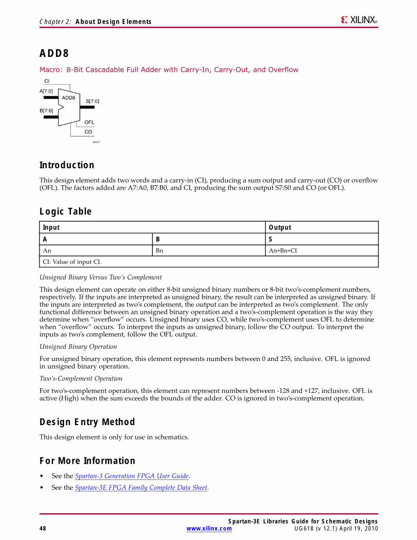
Chapter 2: About Design Elements
ADD8Macro: 8-Bit Cascadable Full Adder with Carry-In, Carry-Out, and Overflow
IntroductionThis design element adds two words and a carry-in (CI), producing a sum output and carry-out (CO) or overflow(OFL). The factors added are A7:A0, B7:B0, and CI, producing the sum output S7:S0 and CO (or OFL).
Logic TableInput Output
A B SAn Bn An+Bn+CI
CI: Value of input CI.
Unsigned Binary Versus Two’s Complement
This design element can operate on either 8-bit unsigned binary numbers or 8-bit two’s-complement numbers,respectively. If the inputs are interpreted as unsigned binary, the result can be interpreted as unsigned binary. Ifthe inputs are interpreted as two’s complement, the output can be interpreted as two’s complement. The onlyfunctional difference between an unsigned binary operation and a two’s-complement operation is the way theydetermine when “overflow” occurs. Unsigned binary uses CO, while two’s-complement uses OFL to determinewhen “overflow” occurs. To interpret the inputs as unsigned binary, follow the CO output. To interpret theinputs as two’s complement, follow the OFL output.
Unsigned Binary Operation
For unsigned binary operation, this element represents numbers between 0 and 255, inclusive. OFL is ignoredin unsigned binary operation.
Two’s-Complement Operation
For two’s-complement operation, this element can represent numbers between -128 and +127, inclusive. OFL isactive (High) when the sum exceeds the bounds of the adder. CO is ignored in two’s-complement operation.
Design Entry MethodThis design element is only for use in schematics.
For More Information• See the Spartan-3 Generation FPGA User Guide.
• See the Spartan-3E FPGA Family Complete Data Sheet.
Spartan-3E Libraries Guide for Schematic Designs48 www.xilinx.com UG618 (v 12.1) April 19, 2010
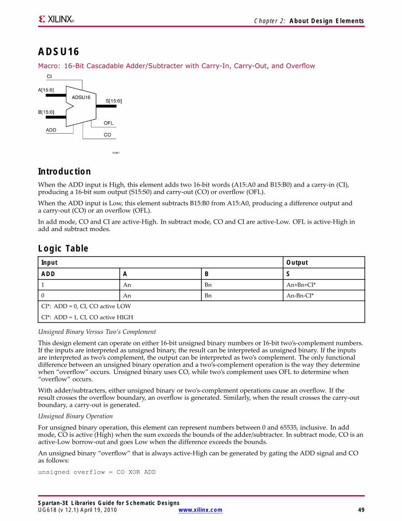
Chapter 2: About Design Elements
ADSU16Macro: 16-Bit Cascadable Adder/Subtracter with Carry-In, Carry-Out, and Overflow
IntroductionWhen the ADD input is High, this element adds two 16-bit words (A15:A0 and B15:B0) and a carry-in (CI),producing a 16-bit sum output (S15:S0) and carry-out (CO) or overflow (OFL).
When the ADD input is Low, this element subtracts B15:B0 from A15:A0, producing a difference output anda carry-out (CO) or an overflow (OFL).
In add mode, CO and CI are active-High. In subtract mode, CO and CI are active-Low. OFL is active-High inadd and subtract modes.
Logic TableInput Output
ADD A B S1 An Bn An+Bn+CI*
0 An Bn An-Bn-CI*
CI*: ADD = 0, CI, CO active LOW
CI*: ADD = 1, CI, CO active HIGH
Unsigned Binary Versus Two’s Complement
This design element can operate on either 16-bit unsigned binary numbers or 16-bit two’s-complement numbers.If the inputs are interpreted as unsigned binary, the result can be interpreted as unsigned binary. If the inputsare interpreted as two’s complement, the output can be interpreted as two’s complement. The only functionaldifference between an unsigned binary operation and a two’s-complement operation is the way they determinewhen “overflow” occurs. Unsigned binary uses CO, while two’s complement uses OFL to determine when“overflow” occurs.
With adder/subtracters, either unsigned binary or two’s-complement operations cause an overflow. If theresult crosses the overflow boundary, an overflow is generated. Similarly, when the result crosses the carry-outboundary, a carry-out is generated.
Unsigned Binary Operation
For unsigned binary operation, this element can represent numbers between 0 and 65535, inclusive. In addmode, CO is active (High) when the sum exceeds the bounds of the adder/subtracter. In subtract mode, CO is anactive-Low borrow-out and goes Low when the difference exceeds the bounds.
An unsigned binary “overflow” that is always active-High can be generated by gating the ADD signal and COas follows:
unsigned overflow = CO XOR ADD
Spartan-3E Libraries Guide for Schematic DesignsUG618 (v 12.1) April 19, 2010 www.xilinx.com 49

Chapter 2: About Design Elements
OFL is ignored in unsigned binary operation.
Two’s-Complement Operation
For two’s-complement operation, this element can represent numbers between -32768 and +32767, inclusive.
If an addition or subtraction operation result exceeds this range, the OFL output goes High. CO is ignored intwo’s-complement operation.
Design Entry MethodThis design element is only for use in schematics.
For More Information• See the Spartan-3 Generation FPGA User Guide.
• See the Spartan-3E FPGA Family Complete Data Sheet.
Spartan-3E Libraries Guide for Schematic Designs50 www.xilinx.com UG618 (v 12.1) April 19, 2010
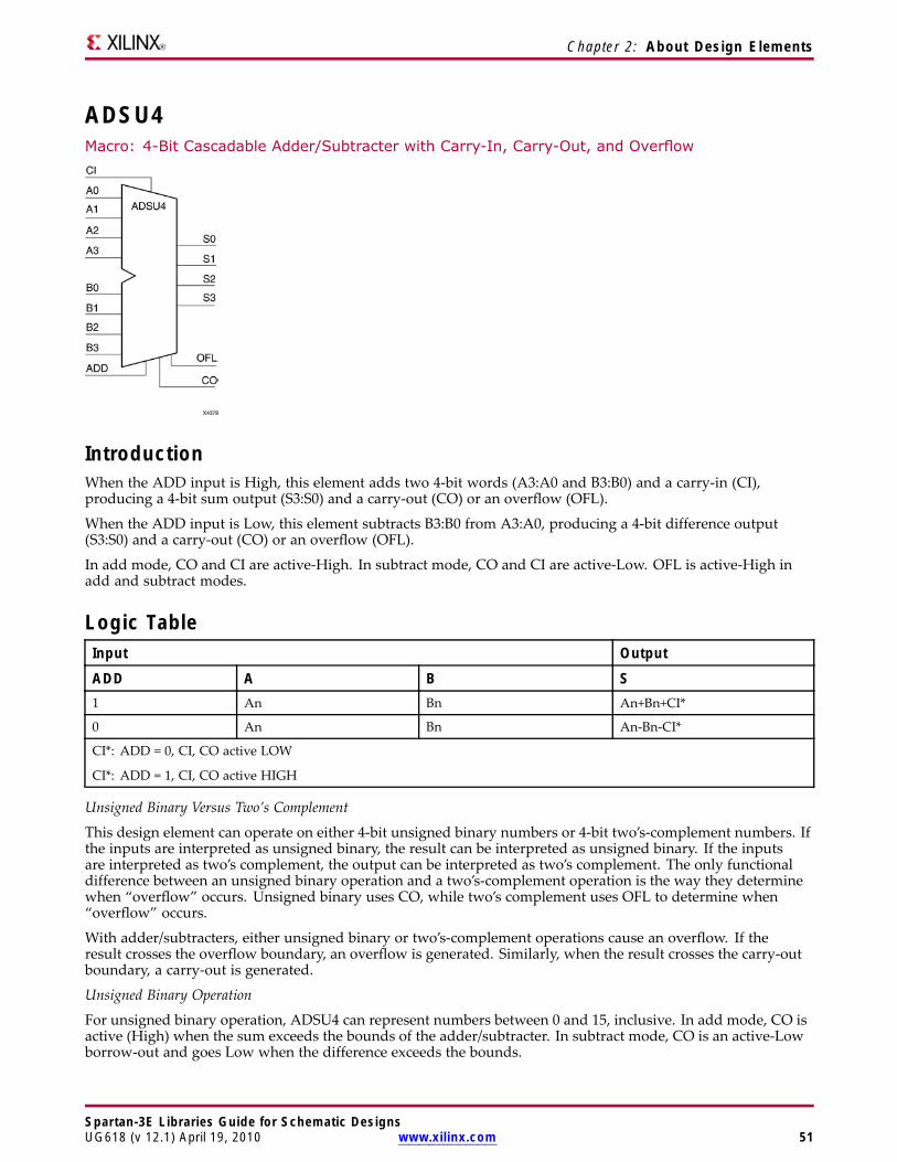
Chapter 2: About Design Elements
ADSU4Macro: 4-Bit Cascadable Adder/Subtracter with Carry-In, Carry-Out, and Overflow
IntroductionWhen the ADD input is High, this element adds two 4-bit words (A3:A0 and B3:B0) and a carry-in (CI),producing a 4-bit sum output (S3:S0) and a carry-out (CO) or an overflow (OFL).
When the ADD input is Low, this element subtracts B3:B0 from A3:A0, producing a 4-bit difference output(S3:S0) and a carry-out (CO) or an overflow (OFL).
In add mode, CO and CI are active-High. In subtract mode, CO and CI are active-Low. OFL is active-High inadd and subtract modes.
Logic TableInput Output
ADD A B S1 An Bn An+Bn+CI*
0 An Bn An-Bn-CI*
CI*: ADD = 0, CI, CO active LOW
CI*: ADD = 1, CI, CO active HIGH
Unsigned Binary Versus Two’s Complement
This design element can operate on either 4-bit unsigned binary numbers or 4-bit two’s-complement numbers. Ifthe inputs are interpreted as unsigned binary, the result can be interpreted as unsigned binary. If the inputsare interpreted as two’s complement, the output can be interpreted as two’s complement. The only functionaldifference between an unsigned binary operation and a two’s-complement operation is the way they determinewhen “overflow” occurs. Unsigned binary uses CO, while two’s complement uses OFL to determine when“overflow” occurs.
With adder/subtracters, either unsigned binary or two’s-complement operations cause an overflow. If theresult crosses the overflow boundary, an overflow is generated. Similarly, when the result crosses the carry-outboundary, a carry-out is generated.
Unsigned Binary Operation
For unsigned binary operation, ADSU4 can represent numbers between 0 and 15, inclusive. In add mode, CO isactive (High) when the sum exceeds the bounds of the adder/subtracter. In subtract mode, CO is an active-Lowborrow-out and goes Low when the difference exceeds the bounds.
Spartan-3E Libraries Guide for Schematic DesignsUG618 (v 12.1) April 19, 2010 www.xilinx.com 51

Chapter 2: About Design Elements
An unsigned binary “overflow” that is always active-High can be generated by gating the ADD signal and COas follows:
unsigned overflow = CO XOR ADD
OFL is ignored in unsigned binary operation.
Two’s-Complement Operation
For two’s-complement operation, this element can represent numbers between -8 and +7, inclusive.
If an addition or subtraction operation result exceeds this range, the OFL output goes High. CO is ignored intwo’s-complement operation.
Design Entry MethodThis design element is only for use in schematics.
For More Information• See the Spartan-3 Generation FPGA User Guide.
• See the Spartan-3E FPGA Family Complete Data Sheet.
Spartan-3E Libraries Guide for Schematic Designs52 www.xilinx.com UG618 (v 12.1) April 19, 2010
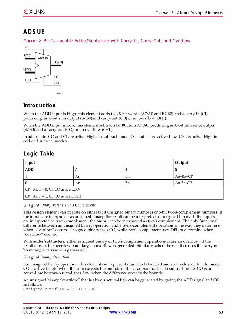
Chapter 2: About Design Elements
ADSU8Macro: 8-Bit Cascadable Adder/Subtracter with Carry-In, Carry-Out, and Overflow
IntroductionWhen the ADD input is High, this element adds two 8-bit words (A7:A0 and B7:B0) and a carry-in (CI),producing, an 8-bit sum output (S7:S0) and carry-out (CO) or an overflow (OFL).
When the ADD input is Low, this element subtracts B7:B0 from A7:A0, producing an 8-bit difference output(S7:S0) and a carry-out (CO) or an overflow (OFL).
In add mode, CO and CI are active-High. In subtract mode, CO and CI are active-Low. OFL is active-High inadd and subtract modes.
Logic TableInput Output
ADD A B S1 An Bn An+Bn+CI*
0 An Bn An-Bn-CI*
CI*: ADD = 0, CI, CO active LOW
CI*: ADD = 1, CI, CO active HIGH
Unsigned Binary Versus Two’s Complement
This design element can operate on either 8-bit unsigned binary numbers or 8-bit two’s-complement numbers. Ifthe inputs are interpreted as unsigned binary, the result can be interpreted as unsigned binary. If the inputsare interpreted as two’s complement, the output can be interpreted as two’s complement. The only functionaldifference between an unsigned binary operation and a two’s-complement operation is the way they determinewhen “overflow” occurs. Unsigned binary uses CO, while two’s complement uses OFL to determine when“overflow” occurs.
With adder/subtracters, either unsigned binary or two’s-complement operations cause an overflow. If theresult crosses the overflow boundary, an overflow is generated. Similarly, when the result crosses the carry-outboundary, a carry-out is generated.
Unsigned Binary Operation
For unsigned binary operation, this element can represent numbers between 0 and 255, inclusive. In add mode,CO is active (High) when the sum exceeds the bounds of the adder/subtracter. In subtract mode, CO is anactive-Low borrow-out and goes Low when the difference exceeds the bounds.
An unsigned binary “overflow” that is always active-High can be generated by gating the ADD signal and COas follows:unsigned overflow = CO XOR ADD
Spartan-3E Libraries Guide for Schematic DesignsUG618 (v 12.1) April 19, 2010 www.xilinx.com 53

Chapter 2: About Design Elements
OFL is ignored in unsigned binary operation.
Two’s-Complement Operation
For two’s-complement operation, this element can represent numbers between -128 and +127, inclusive.
If an addition or subtraction operation result exceeds this range, the OFL output goes High. CO is ignored intwo’s-complement operation.
Design Entry MethodThis design element is only for use in schematics.
For More Information• See the Spartan-3 Generation FPGA User Guide.
• See the Spartan-3E FPGA Family Complete Data Sheet.
Spartan-3E Libraries Guide for Schematic Designs54 www.xilinx.com UG618 (v 12.1) April 19, 2010
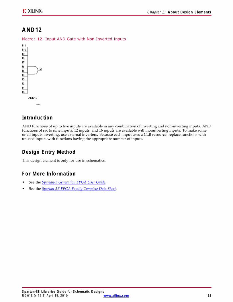
Chapter 2: About Design Elements
AND12Macro: 12- Input AND Gate with Non-Inverted Inputs
IntroductionAND functions of up to five inputs are available in any combination of inverting and non-inverting inputs. ANDfunctions of six to nine inputs, 12 inputs, and 16 inputs are available with noninverting inputs. To make someor all inputs inverting, use external inverters. Because each input uses a CLB resource, replace functions withunused inputs with functions having the appropriate number of inputs.
Design Entry MethodThis design element is only for use in schematics.
For More Information• See the Spartan-3 Generation FPGA User Guide.
• See the Spartan-3E FPGA Family Complete Data Sheet.
Spartan-3E Libraries Guide for Schematic DesignsUG618 (v 12.1) April 19, 2010 www.xilinx.com 55
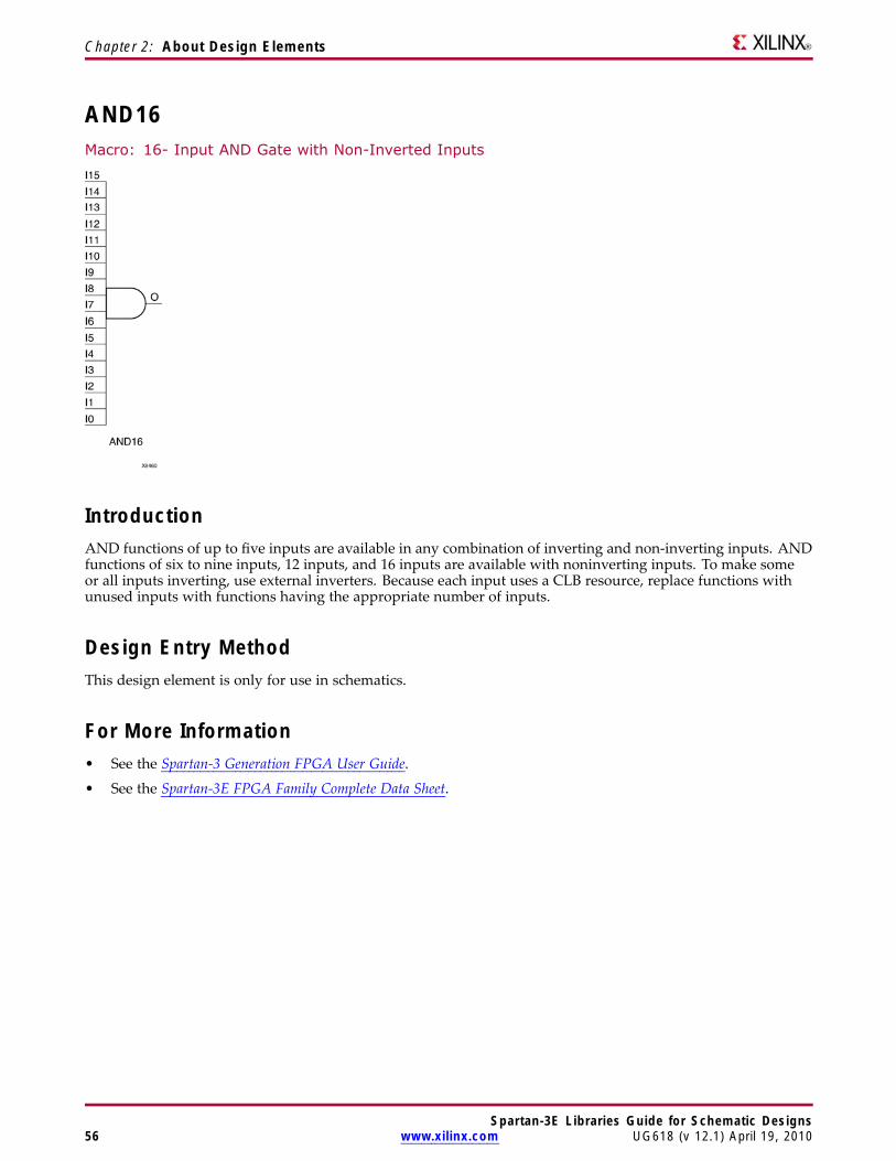
Chapter 2: About Design Elements
AND16Macro: 16- Input AND Gate with Non-Inverted Inputs
IntroductionAND functions of up to five inputs are available in any combination of inverting and non-inverting inputs. ANDfunctions of six to nine inputs, 12 inputs, and 16 inputs are available with noninverting inputs. To make someor all inputs inverting, use external inverters. Because each input uses a CLB resource, replace functions withunused inputs with functions having the appropriate number of inputs.
Design Entry MethodThis design element is only for use in schematics.
For More Information• See the Spartan-3 Generation FPGA User Guide.
• See the Spartan-3E FPGA Family Complete Data Sheet.
Spartan-3E Libraries Guide for Schematic Designs56 www.xilinx.com UG618 (v 12.1) April 19, 2010
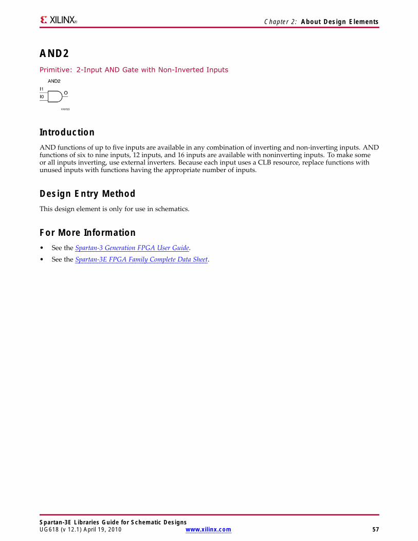
Chapter 2: About Design Elements
AND2Primitive: 2-Input AND Gate with Non-Inverted Inputs
IntroductionAND functions of up to five inputs are available in any combination of inverting and non-inverting inputs. ANDfunctions of six to nine inputs, 12 inputs, and 16 inputs are available with noninverting inputs. To make someor all inputs inverting, use external inverters. Because each input uses a CLB resource, replace functions withunused inputs with functions having the appropriate number of inputs.
Design Entry MethodThis design element is only for use in schematics.
For More Information• See the Spartan-3 Generation FPGA User Guide.
• See the Spartan-3E FPGA Family Complete Data Sheet.
Spartan-3E Libraries Guide for Schematic DesignsUG618 (v 12.1) April 19, 2010 www.xilinx.com 57
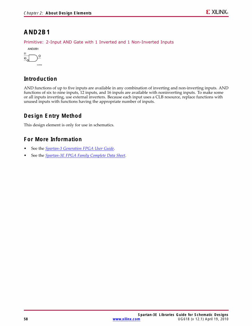
Chapter 2: About Design Elements
AND2B1Primitive: 2-Input AND Gate with 1 Inverted and 1 Non-Inverted Inputs
IntroductionAND functions of up to five inputs are available in any combination of inverting and non-inverting inputs. ANDfunctions of six to nine inputs, 12 inputs, and 16 inputs are available with noninverting inputs. To make someor all inputs inverting, use external inverters. Because each input uses a CLB resource, replace functions withunused inputs with functions having the appropriate number of inputs.
Design Entry MethodThis design element is only for use in schematics.
For More Information• See the Spartan-3 Generation FPGA User Guide.
• See the Spartan-3E FPGA Family Complete Data Sheet.
Spartan-3E Libraries Guide for Schematic Designs58 www.xilinx.com UG618 (v 12.1) April 19, 2010
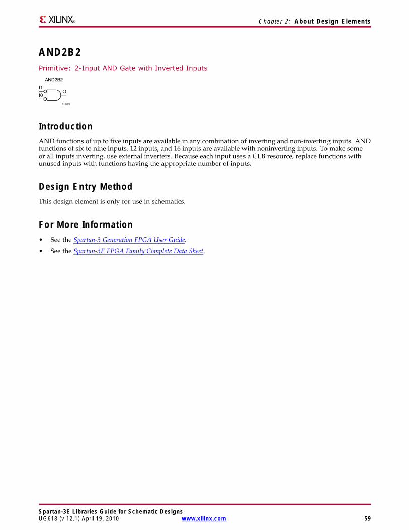
Chapter 2: About Design Elements
AND2B2Primitive: 2-Input AND Gate with Inverted Inputs
IntroductionAND functions of up to five inputs are available in any combination of inverting and non-inverting inputs. ANDfunctions of six to nine inputs, 12 inputs, and 16 inputs are available with noninverting inputs. To make someor all inputs inverting, use external inverters. Because each input uses a CLB resource, replace functions withunused inputs with functions having the appropriate number of inputs.
Design Entry MethodThis design element is only for use in schematics.
For More Information• See the Spartan-3 Generation FPGA User Guide.
• See the Spartan-3E FPGA Family Complete Data Sheet.
Spartan-3E Libraries Guide for Schematic DesignsUG618 (v 12.1) April 19, 2010 www.xilinx.com 59
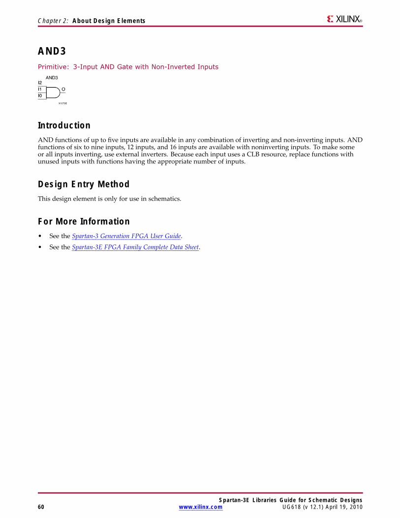
Chapter 2: About Design Elements
AND3Primitive: 3-Input AND Gate with Non-Inverted Inputs
IntroductionAND functions of up to five inputs are available in any combination of inverting and non-inverting inputs. ANDfunctions of six to nine inputs, 12 inputs, and 16 inputs are available with noninverting inputs. To make someor all inputs inverting, use external inverters. Because each input uses a CLB resource, replace functions withunused inputs with functions having the appropriate number of inputs.
Design Entry MethodThis design element is only for use in schematics.
For More Information• See the Spartan-3 Generation FPGA User Guide.
• See the Spartan-3E FPGA Family Complete Data Sheet.
Spartan-3E Libraries Guide for Schematic Designs60 www.xilinx.com UG618 (v 12.1) April 19, 2010
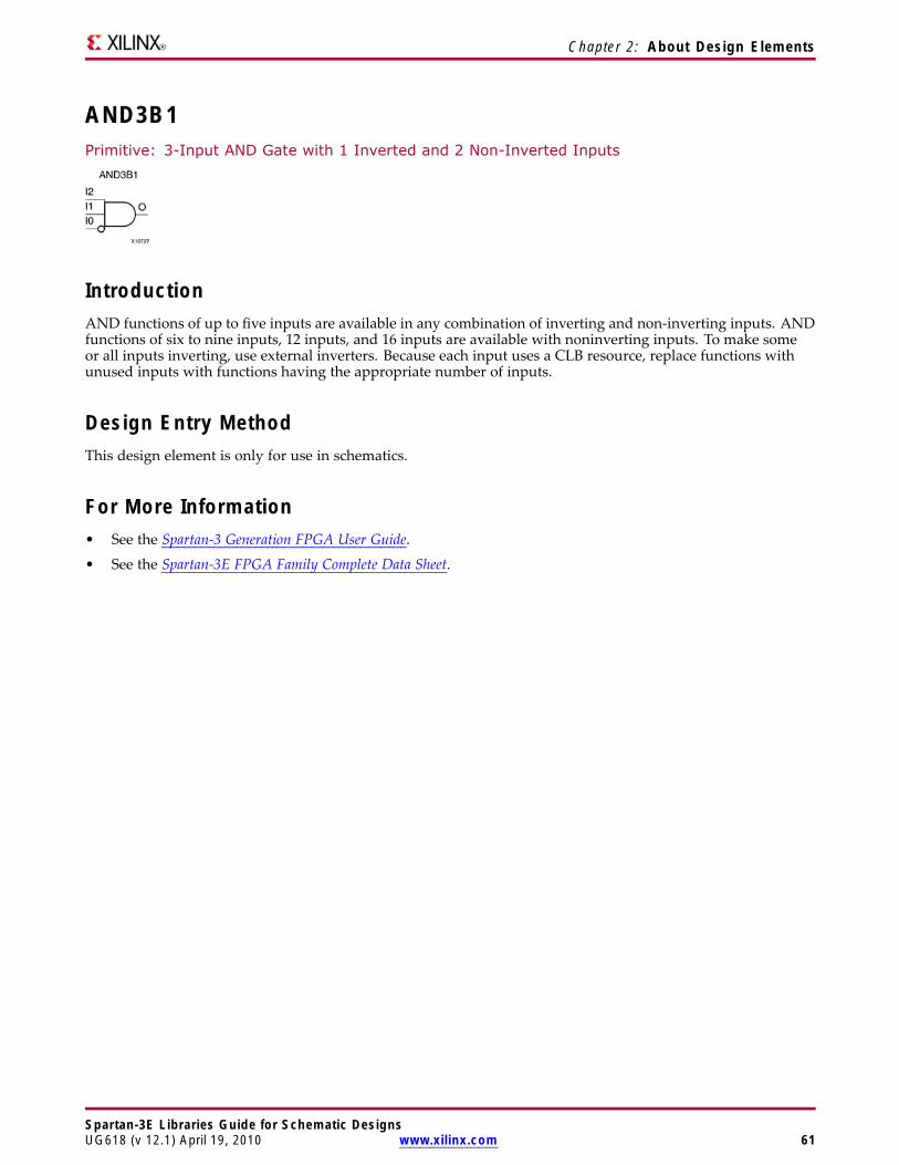
Chapter 2: About Design Elements
AND3B1Primitive: 3-Input AND Gate with 1 Inverted and 2 Non-Inverted Inputs
IntroductionAND functions of up to five inputs are available in any combination of inverting and non-inverting inputs. ANDfunctions of six to nine inputs, 12 inputs, and 16 inputs are available with noninverting inputs. To make someor all inputs inverting, use external inverters. Because each input uses a CLB resource, replace functions withunused inputs with functions having the appropriate number of inputs.
Design Entry MethodThis design element is only for use in schematics.
For More Information• See the Spartan-3 Generation FPGA User Guide.
• See the Spartan-3E FPGA Family Complete Data Sheet.
Spartan-3E Libraries Guide for Schematic DesignsUG618 (v 12.1) April 19, 2010 www.xilinx.com 61

Chapter 2: About Design Elements
AND3B2Primitive: 3-Input AND Gate with 2 Inverted and 1 Non-Inverted Inputs
IntroductionAND functions of up to five inputs are available in any combination of inverting and non-inverting inputs. ANDfunctions of six to nine inputs, 12 inputs, and 16 inputs are available with noninverting inputs. To make someor all inputs inverting, use external inverters. Because each input uses a CLB resource, replace functions withunused inputs with functions having the appropriate number of inputs.
Design Entry MethodThis design element is only for use in schematics.
For More Information• See the Spartan-3 Generation FPGA User Guide.
• See the Spartan-3E FPGA Family Complete Data Sheet.
Spartan-3E Libraries Guide for Schematic Designs62 www.xilinx.com UG618 (v 12.1) April 19, 2010
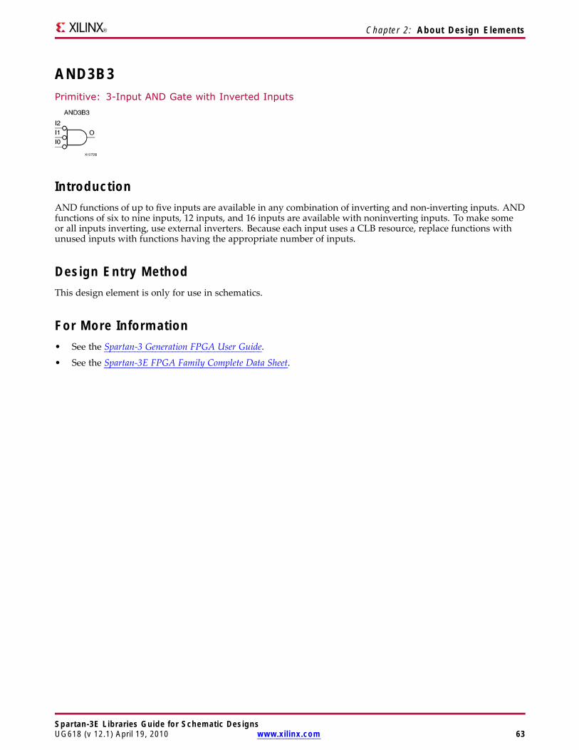
Chapter 2: About Design Elements
AND3B3Primitive: 3-Input AND Gate with Inverted Inputs
IntroductionAND functions of up to five inputs are available in any combination of inverting and non-inverting inputs. ANDfunctions of six to nine inputs, 12 inputs, and 16 inputs are available with noninverting inputs. To make someor all inputs inverting, use external inverters. Because each input uses a CLB resource, replace functions withunused inputs with functions having the appropriate number of inputs.
Design Entry MethodThis design element is only for use in schematics.
For More Information• See the Spartan-3 Generation FPGA User Guide.
• See the Spartan-3E FPGA Family Complete Data Sheet.
Spartan-3E Libraries Guide for Schematic DesignsUG618 (v 12.1) April 19, 2010 www.xilinx.com 63
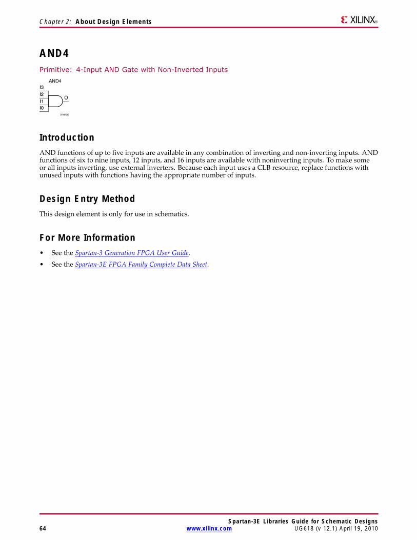
Chapter 2: About Design Elements
AND4Primitive: 4-Input AND Gate with Non-Inverted Inputs
IntroductionAND functions of up to five inputs are available in any combination of inverting and non-inverting inputs. ANDfunctions of six to nine inputs, 12 inputs, and 16 inputs are available with noninverting inputs. To make someor all inputs inverting, use external inverters. Because each input uses a CLB resource, replace functions withunused inputs with functions having the appropriate number of inputs.
Design Entry MethodThis design element is only for use in schematics.
For More Information• See the Spartan-3 Generation FPGA User Guide.
• See the Spartan-3E FPGA Family Complete Data Sheet.
Spartan-3E Libraries Guide for Schematic Designs64 www.xilinx.com UG618 (v 12.1) April 19, 2010
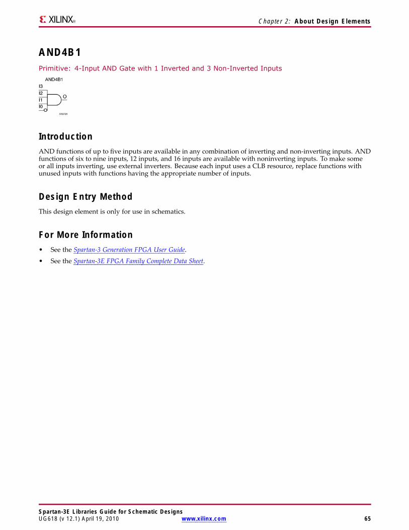
Chapter 2: About Design Elements
AND4B1Primitive: 4-Input AND Gate with 1 Inverted and 3 Non-Inverted Inputs
IntroductionAND functions of up to five inputs are available in any combination of inverting and non-inverting inputs. ANDfunctions of six to nine inputs, 12 inputs, and 16 inputs are available with noninverting inputs. To make someor all inputs inverting, use external inverters. Because each input uses a CLB resource, replace functions withunused inputs with functions having the appropriate number of inputs.
Design Entry MethodThis design element is only for use in schematics.
For More Information• See the Spartan-3 Generation FPGA User Guide.
• See the Spartan-3E FPGA Family Complete Data Sheet.
Spartan-3E Libraries Guide for Schematic DesignsUG618 (v 12.1) April 19, 2010 www.xilinx.com 65

Chapter 2: About Design Elements
AND4B2Primitive: 4-Input AND Gate with 2 Inverted and 2 Non-Inverted Inputs
IntroductionAND functions of up to five inputs are available in any combination of inverting and non-inverting inputs. ANDfunctions of six to nine inputs, 12 inputs, and 16 inputs are available with noninverting inputs. To make someor all inputs inverting, use external inverters. Because each input uses a CLB resource, replace functions withunused inputs with functions having the appropriate number of inputs.
Design Entry MethodThis design element is only for use in schematics.
For More Information• See the Spartan-3 Generation FPGA User Guide.
• See the Spartan-3E FPGA Family Complete Data Sheet.
Spartan-3E Libraries Guide for Schematic Designs66 www.xilinx.com UG618 (v 12.1) April 19, 2010
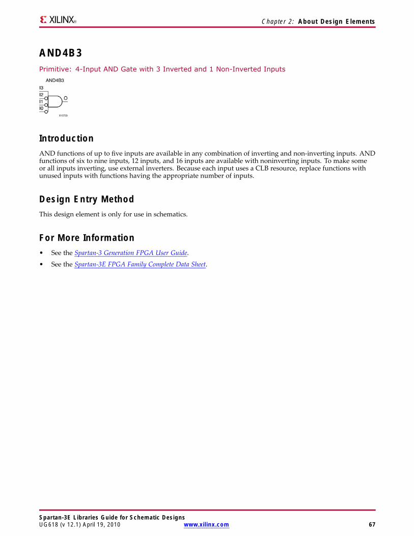
Chapter 2: About Design Elements
AND4B3Primitive: 4-Input AND Gate with 3 Inverted and 1 Non-Inverted Inputs
IntroductionAND functions of up to five inputs are available in any combination of inverting and non-inverting inputs. ANDfunctions of six to nine inputs, 12 inputs, and 16 inputs are available with noninverting inputs. To make someor all inputs inverting, use external inverters. Because each input uses a CLB resource, replace functions withunused inputs with functions having the appropriate number of inputs.
Design Entry MethodThis design element is only for use in schematics.
For More Information• See the Spartan-3 Generation FPGA User Guide.
• See the Spartan-3E FPGA Family Complete Data Sheet.
Spartan-3E Libraries Guide for Schematic DesignsUG618 (v 12.1) April 19, 2010 www.xilinx.com 67
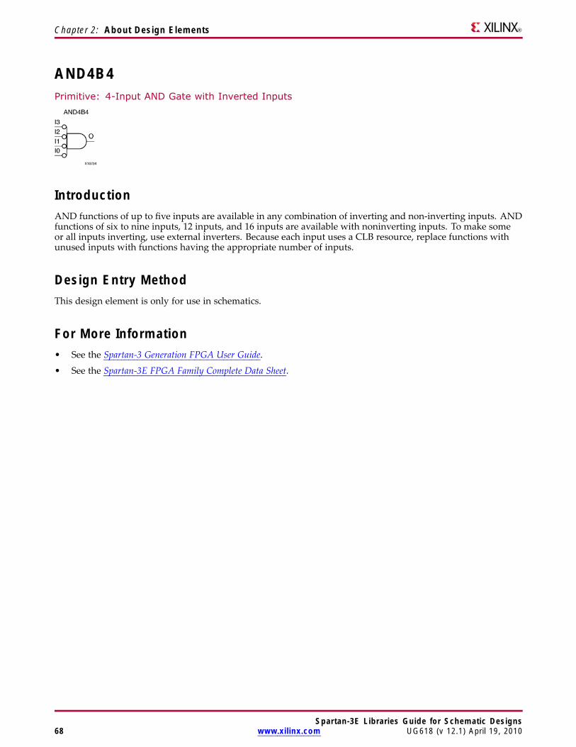
Chapter 2: About Design Elements
AND4B4Primitive: 4-Input AND Gate with Inverted Inputs
IntroductionAND functions of up to five inputs are available in any combination of inverting and non-inverting inputs. ANDfunctions of six to nine inputs, 12 inputs, and 16 inputs are available with noninverting inputs. To make someor all inputs inverting, use external inverters. Because each input uses a CLB resource, replace functions withunused inputs with functions having the appropriate number of inputs.
Design Entry MethodThis design element is only for use in schematics.
For More Information• See the Spartan-3 Generation FPGA User Guide.
• See the Spartan-3E FPGA Family Complete Data Sheet.
Spartan-3E Libraries Guide for Schematic Designs68 www.xilinx.com UG618 (v 12.1) April 19, 2010
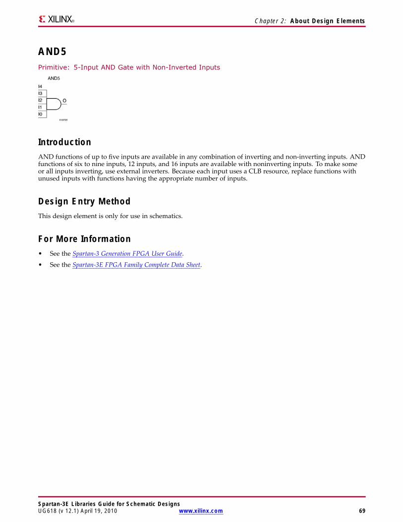
Chapter 2: About Design Elements
AND5Primitive: 5-Input AND Gate with Non-Inverted Inputs
IntroductionAND functions of up to five inputs are available in any combination of inverting and non-inverting inputs. ANDfunctions of six to nine inputs, 12 inputs, and 16 inputs are available with noninverting inputs. To make someor all inputs inverting, use external inverters. Because each input uses a CLB resource, replace functions withunused inputs with functions having the appropriate number of inputs.
Design Entry MethodThis design element is only for use in schematics.
For More Information• See the Spartan-3 Generation FPGA User Guide.
• See the Spartan-3E FPGA Family Complete Data Sheet.
Spartan-3E Libraries Guide for Schematic DesignsUG618 (v 12.1) April 19, 2010 www.xilinx.com 69

Chapter 2: About Design Elements
AND5B1Primitive: 5-Input AND Gate with 1 Inverted and 4 Non-Inverted Inputs
IntroductionAND functions of up to five inputs are available in any combination of inverting and non-inverting inputs. ANDfunctions of six to nine inputs, 12 inputs, and 16 inputs are available with noninverting inputs. To make someor all inputs inverting, use external inverters. Because each input uses a CLB resource, replace functions withunused inputs with functions having the appropriate number of inputs.
Design Entry MethodThis design element is only for use in schematics.
For More Information• See the Spartan-3 Generation FPGA User Guide.
• See the Spartan-3E FPGA Family Complete Data Sheet.
Spartan-3E Libraries Guide for Schematic Designs70 www.xilinx.com UG618 (v 12.1) April 19, 2010
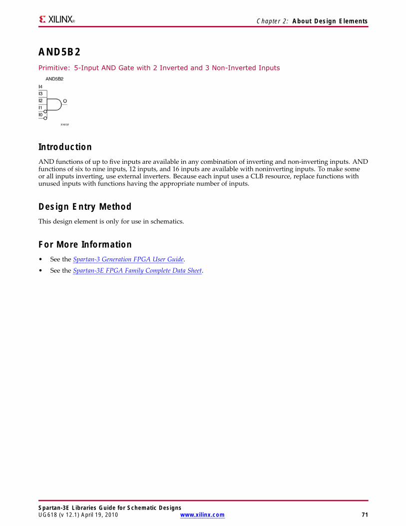
Chapter 2: About Design Elements
AND5B2Primitive: 5-Input AND Gate with 2 Inverted and 3 Non-Inverted Inputs
IntroductionAND functions of up to five inputs are available in any combination of inverting and non-inverting inputs. ANDfunctions of six to nine inputs, 12 inputs, and 16 inputs are available with noninverting inputs. To make someor all inputs inverting, use external inverters. Because each input uses a CLB resource, replace functions withunused inputs with functions having the appropriate number of inputs.
Design Entry MethodThis design element is only for use in schematics.
For More Information• See the Spartan-3 Generation FPGA User Guide.
• See the Spartan-3E FPGA Family Complete Data Sheet.
Spartan-3E Libraries Guide for Schematic DesignsUG618 (v 12.1) April 19, 2010 www.xilinx.com 71
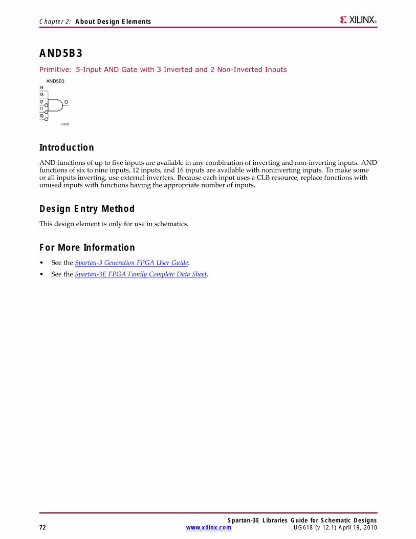
Chapter 2: About Design Elements
AND5B3Primitive: 5-Input AND Gate with 3 Inverted and 2 Non-Inverted Inputs
IntroductionAND functions of up to five inputs are available in any combination of inverting and non-inverting inputs. ANDfunctions of six to nine inputs, 12 inputs, and 16 inputs are available with noninverting inputs. To make someor all inputs inverting, use external inverters. Because each input uses a CLB resource, replace functions withunused inputs with functions having the appropriate number of inputs.
Design Entry MethodThis design element is only for use in schematics.
For More Information• See the Spartan-3 Generation FPGA User Guide.
• See the Spartan-3E FPGA Family Complete Data Sheet.
Spartan-3E Libraries Guide for Schematic Designs72 www.xilinx.com UG618 (v 12.1) April 19, 2010
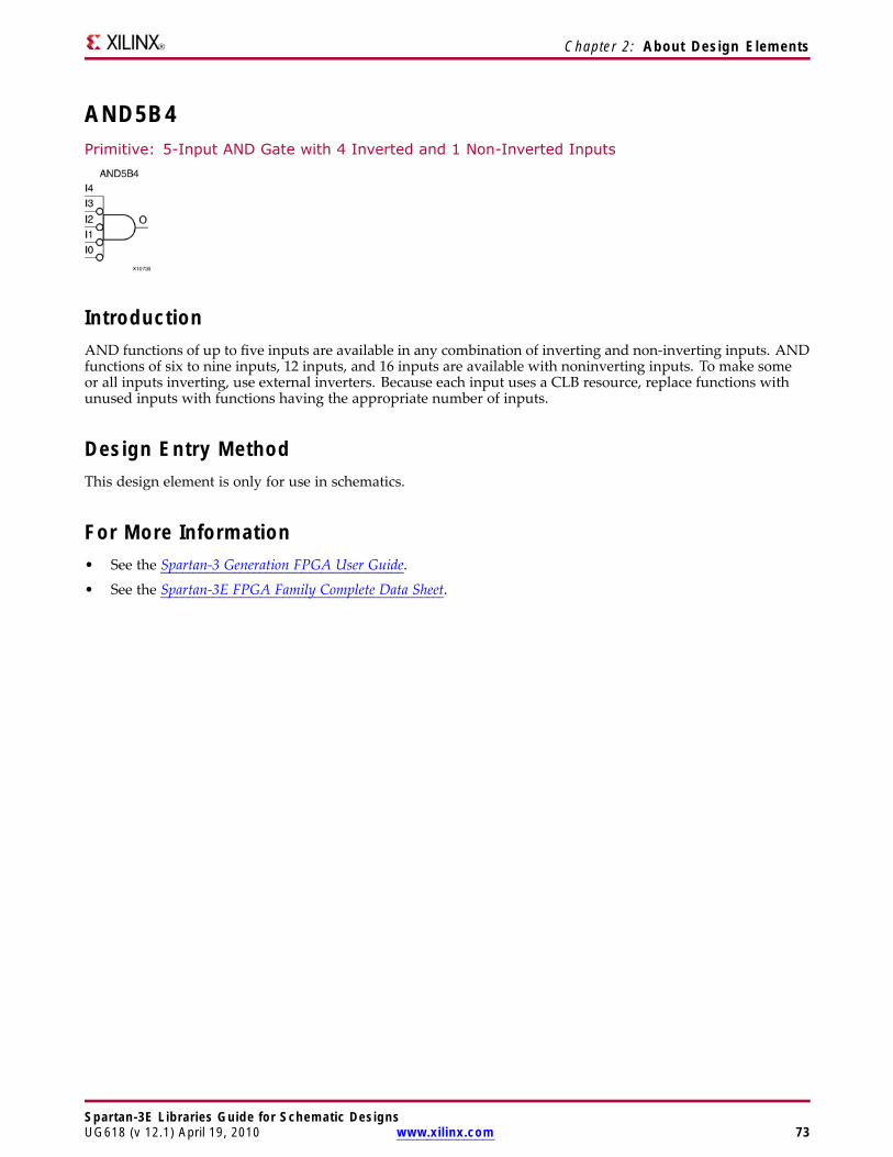
Chapter 2: About Design Elements
AND5B4Primitive: 5-Input AND Gate with 4 Inverted and 1 Non-Inverted Inputs
IntroductionAND functions of up to five inputs are available in any combination of inverting and non-inverting inputs. ANDfunctions of six to nine inputs, 12 inputs, and 16 inputs are available with noninverting inputs. To make someor all inputs inverting, use external inverters. Because each input uses a CLB resource, replace functions withunused inputs with functions having the appropriate number of inputs.
Design Entry MethodThis design element is only for use in schematics.
For More Information• See the Spartan-3 Generation FPGA User Guide.
• See the Spartan-3E FPGA Family Complete Data Sheet.
Spartan-3E Libraries Guide for Schematic DesignsUG618 (v 12.1) April 19, 2010 www.xilinx.com 73
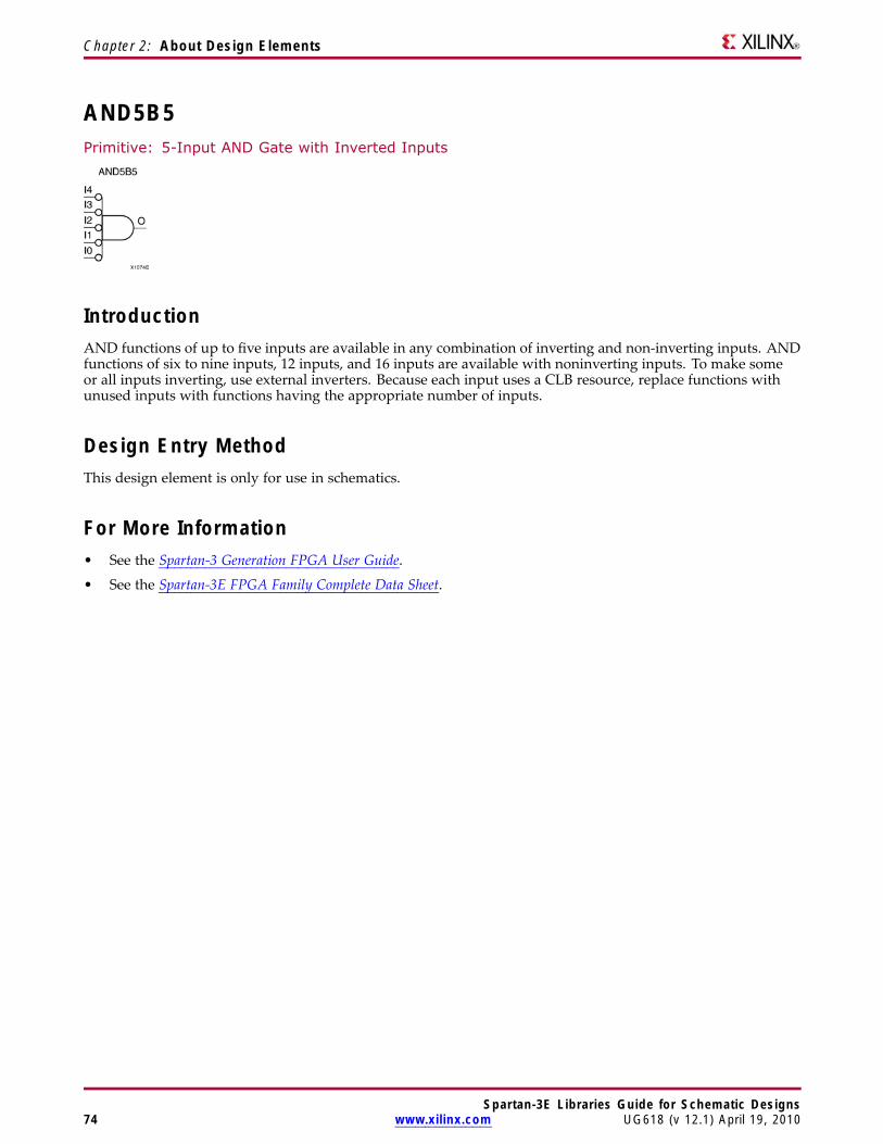
Chapter 2: About Design Elements
AND5B5Primitive: 5-Input AND Gate with Inverted Inputs
IntroductionAND functions of up to five inputs are available in any combination of inverting and non-inverting inputs. ANDfunctions of six to nine inputs, 12 inputs, and 16 inputs are available with noninverting inputs. To make someor all inputs inverting, use external inverters. Because each input uses a CLB resource, replace functions withunused inputs with functions having the appropriate number of inputs.
Design Entry MethodThis design element is only for use in schematics.
For More Information• See the Spartan-3 Generation FPGA User Guide.
• See the Spartan-3E FPGA Family Complete Data Sheet.
Spartan-3E Libraries Guide for Schematic Designs74 www.xilinx.com UG618 (v 12.1) April 19, 2010
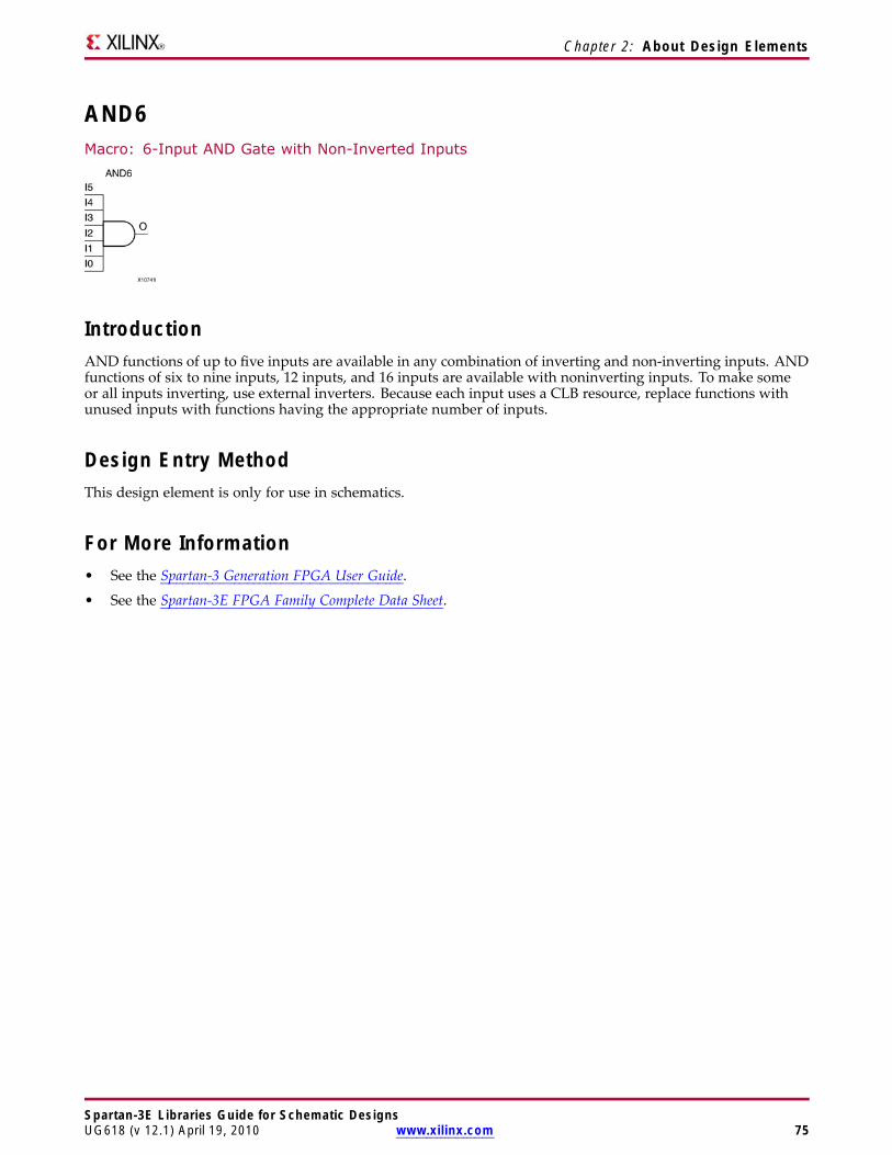
Chapter 2: About Design Elements
AND6Macro: 6-Input AND Gate with Non-Inverted Inputs
IntroductionAND functions of up to five inputs are available in any combination of inverting and non-inverting inputs. ANDfunctions of six to nine inputs, 12 inputs, and 16 inputs are available with noninverting inputs. To make someor all inputs inverting, use external inverters. Because each input uses a CLB resource, replace functions withunused inputs with functions having the appropriate number of inputs.
Design Entry MethodThis design element is only for use in schematics.
For More Information• See the Spartan-3 Generation FPGA User Guide.
• See the Spartan-3E FPGA Family Complete Data Sheet.
Spartan-3E Libraries Guide for Schematic DesignsUG618 (v 12.1) April 19, 2010 www.xilinx.com 75
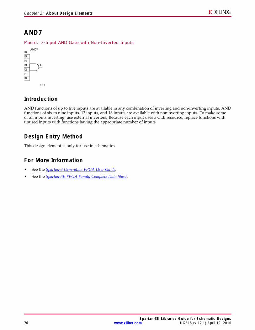
Chapter 2: About Design Elements
AND7Macro: 7-Input AND Gate with Non-Inverted Inputs
IntroductionAND functions of up to five inputs are available in any combination of inverting and non-inverting inputs. ANDfunctions of six to nine inputs, 12 inputs, and 16 inputs are available with noninverting inputs. To make someor all inputs inverting, use external inverters. Because each input uses a CLB resource, replace functions withunused inputs with functions having the appropriate number of inputs.
Design Entry MethodThis design element is only for use in schematics.
For More Information• See the Spartan-3 Generation FPGA User Guide.
• See the Spartan-3E FPGA Family Complete Data Sheet.
Spartan-3E Libraries Guide for Schematic Designs76 www.xilinx.com UG618 (v 12.1) April 19, 2010
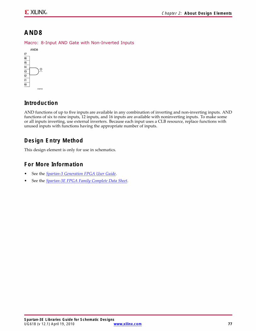
Chapter 2: About Design Elements
AND8Macro: 8-Input AND Gate with Non-Inverted Inputs
IntroductionAND functions of up to five inputs are available in any combination of inverting and non-inverting inputs. ANDfunctions of six to nine inputs, 12 inputs, and 16 inputs are available with noninverting inputs. To make someor all inputs inverting, use external inverters. Because each input uses a CLB resource, replace functions withunused inputs with functions having the appropriate number of inputs.
Design Entry MethodThis design element is only for use in schematics.
For More Information• See the Spartan-3 Generation FPGA User Guide.
• See the Spartan-3E FPGA Family Complete Data Sheet.
Spartan-3E Libraries Guide for Schematic DesignsUG618 (v 12.1) April 19, 2010 www.xilinx.com 77
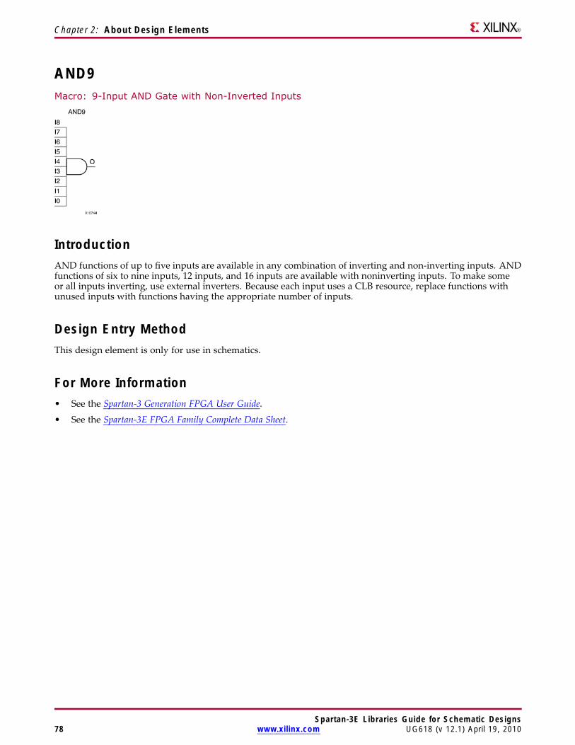
Chapter 2: About Design Elements
AND9Macro: 9-Input AND Gate with Non-Inverted Inputs
IntroductionAND functions of up to five inputs are available in any combination of inverting and non-inverting inputs. ANDfunctions of six to nine inputs, 12 inputs, and 16 inputs are available with noninverting inputs. To make someor all inputs inverting, use external inverters. Because each input uses a CLB resource, replace functions withunused inputs with functions having the appropriate number of inputs.
Design Entry MethodThis design element is only for use in schematics.
For More Information• See the Spartan-3 Generation FPGA User Guide.
• See the Spartan-3E FPGA Family Complete Data Sheet.
Spartan-3E Libraries Guide for Schematic Designs78 www.xilinx.com UG618 (v 12.1) April 19, 2010
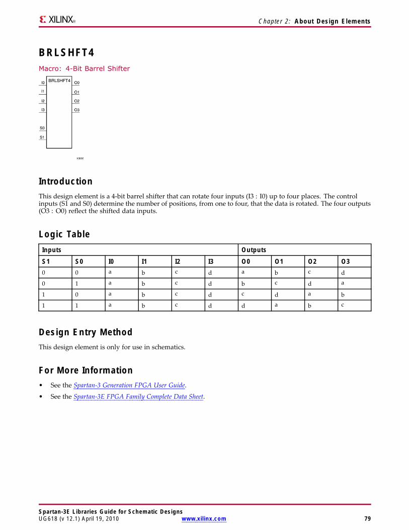
Chapter 2: About Design Elements
BRLSHFT4Macro: 4-Bit Barrel Shifter
IntroductionThis design element is a 4-bit barrel shifter that can rotate four inputs (I3 : I0) up to four places. The controlinputs (S1 and S0) determine the number of positions, from one to four, that the data is rotated. The four outputs(O3 : O0) reflect the shifted data inputs.
Logic TableInputs Outputs
S1 S0 I0 I1 I2 I3 O0 O1 O2 O30 0 a b c d a b c d
0 1 a b c d b c d a
1 0 a b c d c d a b
1 1 a b c d d a b c
Design Entry MethodThis design element is only for use in schematics.
For More Information• See the Spartan-3 Generation FPGA User Guide.
• See the Spartan-3E FPGA Family Complete Data Sheet.
Spartan-3E Libraries Guide for Schematic DesignsUG618 (v 12.1) April 19, 2010 www.xilinx.com 79
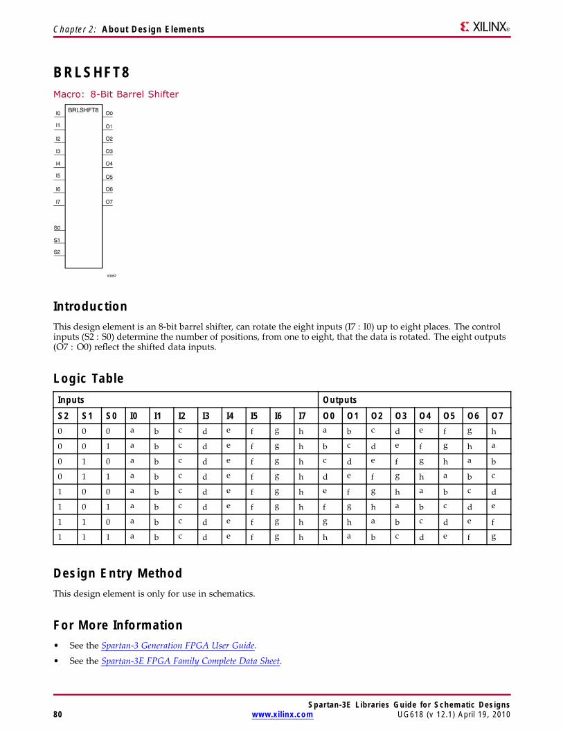
Chapter 2: About Design Elements
BRLSHFT8Macro: 8-Bit Barrel Shifter
IntroductionThis design element is an 8-bit barrel shifter, can rotate the eight inputs (I7 : I0) up to eight places. The controlinputs (S2 : S0) determine the number of positions, from one to eight, that the data is rotated. The eight outputs(O7 : O0) reflect the shifted data inputs.
Logic TableInputs Outputs
S2 S1 S0 I0 I1 I2 I3 I4 I5 I6 I7 O0 O1 O2 O3 O4 O5 O6 O70 0 0 a b c d e f g h a b c d e f g h
0 0 1 a b c d e f g h b c d e f g h a
0 1 0 a b c d e f g h c d e f g h a b
0 1 1 a b c d e f g h d e f g h a b c
1 0 0 a b c d e f g h e f g h a b c d
1 0 1 a b c d e f g h f g h a b c d e
1 1 0 a b c d e f g h g h a b c d e f
1 1 1 a b c d e f g h h a b c d e f g
Design Entry MethodThis design element is only for use in schematics.
For More Information• See the Spartan-3 Generation FPGA User Guide.
• See the Spartan-3E FPGA Family Complete Data Sheet.
Spartan-3E Libraries Guide for Schematic Designs80 www.xilinx.com UG618 (v 12.1) April 19, 2010
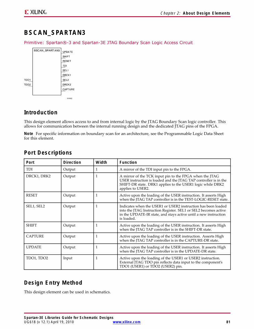
Chapter 2: About Design Elements
BSCAN_SPARTAN3Primitive: Spartan®-3 and Spartan-3E JTAG Boundary Scan Logic Access Circuit
IntroductionThis design element allows access to and from internal logic by the JTAG Boundary Scan logic controller. Thisallows for communication between the internal running design and the dedicated JTAG pins of the FPGA.
Note For specific information on boundary scan for an architecture, see the Programmable Logic Data Sheetfor this element.
Port DescriptionsPort Direction Width FunctionTDI Output 1 A mirror of the TDI input pin to the FPGA.
DRCK1, DRK2 Output 1 A mirror of the TCK input pin to the FPGA when the JTAGUSER instruction is loaded and the JTAG TAP controller is in theSHIFT-DR state. DRK1 applies to the USER1 logic while DRK2applies to USER2.
RESET Output 1 Active upon the loading of the USER instruction. It asserts Highwhen the JTAG TAP controller is in the TEST-LOGIC-RESET state.
SEL1, SEL2 Output 1 Indicates when the USER1 or USER2 instruction has been loadedinto the JTAG Instruction Register. SEL1 or SEL2 becomes activein the UPDATE-IR state, and stays active until a new instructionis loaded.
SHIFT Output 1 Active upon the loading of the USER instruction. It asserts Highwhen the JTAG TAP controller is in the SHIFT-DR state.
CAPTURE Output 1 Active upon the loading of the USER instruction. Asserts Highwhen the JTAG TAP controller is in the CAPTURE-DR state.
UPDATE Output 1 Active upon the loading of the USER instruction. It asserts Highwhen the JTAG TAP controller is in the UPDATE-DR state.
TDO1, TDO2 Input 1 Active upon the loading of the USER1 or USER2 instruction.External JTAG TDO pin reflects data input to the component’sTDO1 (USER1) or TDO2 (USER2) pin.
Design Entry MethodThis design element can be used in schematics.
Spartan-3E Libraries Guide for Schematic DesignsUG618 (v 12.1) April 19, 2010 www.xilinx.com 81

Chapter 2: About Design Elements
For More Information• See the Spartan-3 Generation FPGA User Guide.
• See the Spartan-3E FPGA Family Complete Data Sheet.
Spartan-3E Libraries Guide for Schematic Designs82 www.xilinx.com UG618 (v 12.1) April 19, 2010
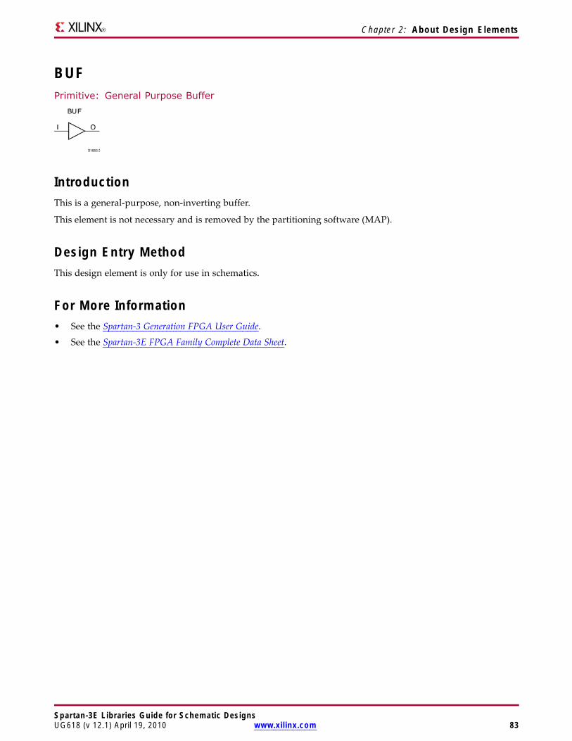
Chapter 2: About Design Elements
BUFPrimitive: General Purpose Buffer
IntroductionThis is a general-purpose, non-inverting buffer.
This element is not necessary and is removed by the partitioning software (MAP).
Design Entry MethodThis design element is only for use in schematics.
For More Information• See the Spartan-3 Generation FPGA User Guide.
• See the Spartan-3E FPGA Family Complete Data Sheet.
Spartan-3E Libraries Guide for Schematic DesignsUG618 (v 12.1) April 19, 2010 www.xilinx.com 83

Chapter 2: About Design Elements
BUFCFPrimitive: Fast Connect Buffer
IntroductionThis design element is a single fast connect buffer used to connect the outputs of the LUTs and some dedicatedlogic directly to the input of another LUT. Using this buffer implies CLB packing. No more than four LUTsmay be connected together as a group.
Design Entry MethodThis design element can be used in schematics.
For More Information• See the Spartan-3 Generation FPGA User Guide.
• See the Spartan-3E FPGA Family Complete Data Sheet.
Spartan-3E Libraries Guide for Schematic Designs84 www.xilinx.com UG618 (v 12.1) April 19, 2010
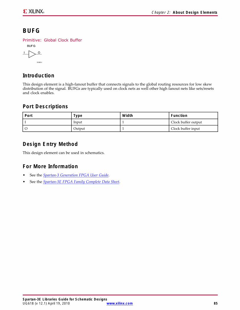
Chapter 2: About Design Elements
BUFGPrimitive: Global Clock Buffer
IntroductionThis design element is a high-fanout buffer that connects signals to the global routing resources for low skewdistribution of the signal. BUFGs are typically used on clock nets as well other high fanout nets like sets/resetsand clock enables.
Port DescriptionsPort Type Width FunctionI Input 1 Clock buffer output
O Output 1 Clock buffer input
Design Entry MethodThis design element can be used in schematics.
For More Information• See the Spartan-3 Generation FPGA User Guide.
• See the Spartan-3E FPGA Family Complete Data Sheet.
Spartan-3E Libraries Guide for Schematic DesignsUG618 (v 12.1) April 19, 2010 www.xilinx.com 85
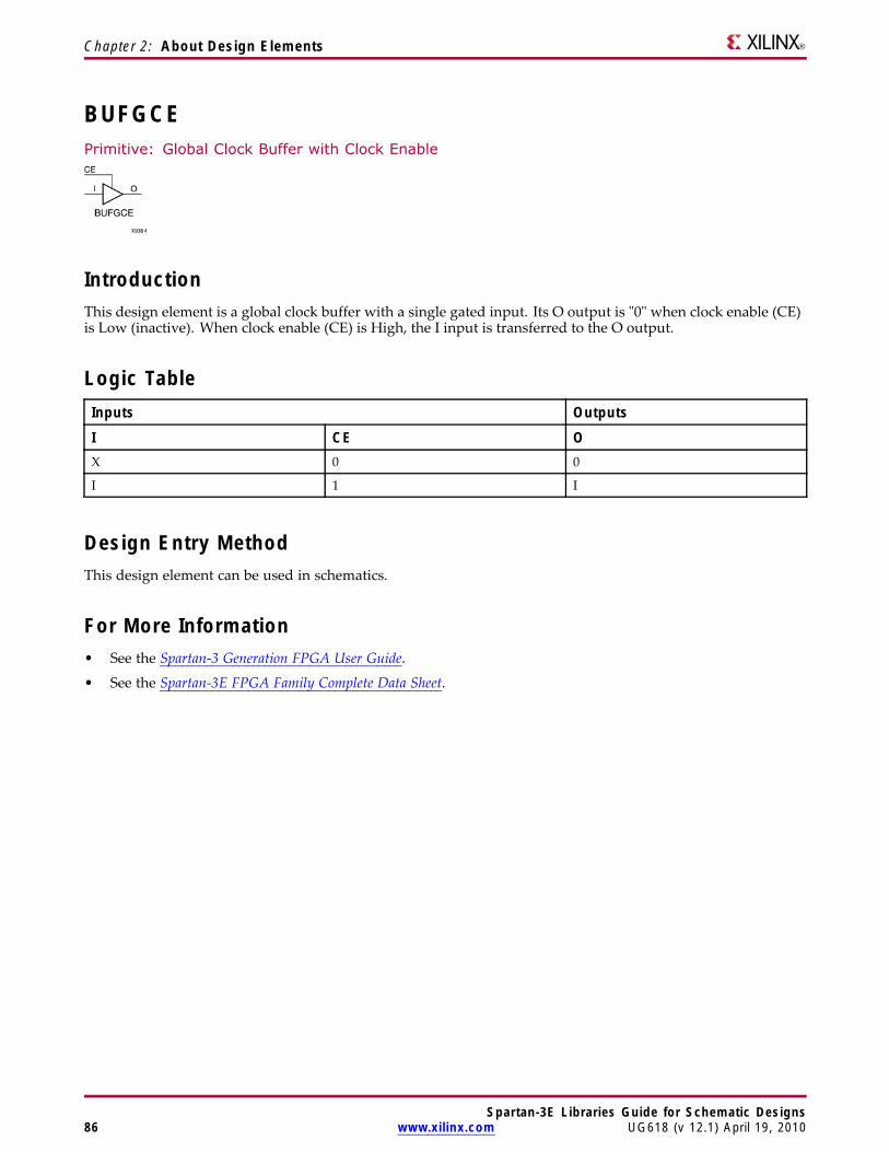
Chapter 2: About Design Elements
BUFGCEPrimitive: Global Clock Buffer with Clock Enable
IntroductionThis design element is a global clock buffer with a single gated input. Its O output is "0" when clock enable (CE)is Low (inactive). When clock enable (CE) is High, the I input is transferred to the O output.
Logic TableInputs Outputs
I CE OX 0 0
I 1 I
Design Entry MethodThis design element can be used in schematics.
For More Information• See the Spartan-3 Generation FPGA User Guide.
• See the Spartan-3E FPGA Family Complete Data Sheet.
Spartan-3E Libraries Guide for Schematic Designs86 www.xilinx.com UG618 (v 12.1) April 19, 2010
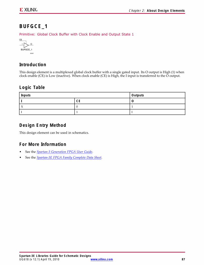
Chapter 2: About Design Elements
BUFGCE_1Primitive: Global Clock Buffer with Clock Enable and Output State 1
IntroductionThis design element is a multiplexed global clock buffer with a single gated input. Its O output is High (1) whenclock enable (CE) is Low (inactive). When clock enable (CE) is High, the I input is transferred to the O output.
Logic TableInputs Outputs
I CE OX 0 1
I 1 I
Design Entry MethodThis design element can be used in schematics.
For More Information• See the Spartan-3 Generation FPGA User Guide.
• See the Spartan-3E FPGA Family Complete Data Sheet.
Spartan-3E Libraries Guide for Schematic DesignsUG618 (v 12.1) April 19, 2010 www.xilinx.com 87
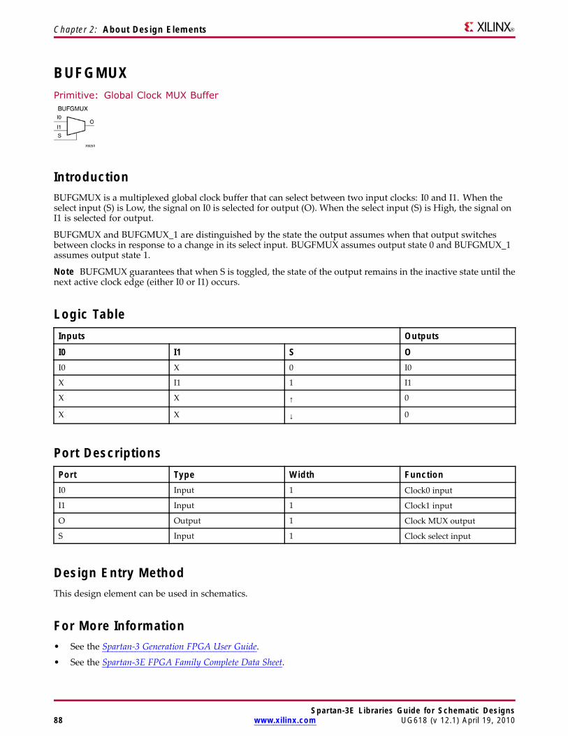
Chapter 2: About Design Elements
BUFGMUXPrimitive: Global Clock MUX Buffer
IntroductionBUFGMUX is a multiplexed global clock buffer that can select between two input clocks: I0 and I1. When theselect input (S) is Low, the signal on I0 is selected for output (O). When the select input (S) is High, the signal onI1 is selected for output.
BUFGMUX and BUFGMUX_1 are distinguished by the state the output assumes when that output switchesbetween clocks in response to a change in its select input. BUGFMUX assumes output state 0 and BUFGMUX_1assumes output state 1.
Note BUFGMUX guarantees that when S is toggled, the state of the output remains in the inactive state until thenext active clock edge (either I0 or I1) occurs.
Logic TableInputs Outputs
I0 I1 S OI0 X 0 I0
X I1 1 I1
X X ↑ 0
X X ↓ 0
Port DescriptionsPort Type Width FunctionI0 Input 1 Clock0 input
I1 Input 1 Clock1 input
O Output 1 Clock MUX output
S Input 1 Clock select input
Design Entry MethodThis design element can be used in schematics.
For More Information• See the Spartan-3 Generation FPGA User Guide.
• See the Spartan-3E FPGA Family Complete Data Sheet.
Spartan-3E Libraries Guide for Schematic Designs88 www.xilinx.com UG618 (v 12.1) April 19, 2010
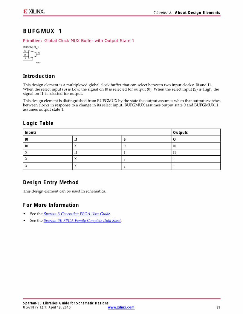
Chapter 2: About Design Elements
BUFGMUX_1Primitive: Global Clock MUX Buffer with Output State 1
IntroductionThis design element is a multiplexed global clock buffer that can select between two input clocks: I0 and I1.When the select input (S) is Low, the signal on I0 is selected for output (0). When the select input (S) is High, thesignal on I1 is selected for output.
This design element is distinguished from BUFGMUX by the state the output assumes when that output switchesbetween clocks in response to a change in its select input. BUFGMUX assumes output state 0 and BUFGMUX_1assumes output state 1.
Logic TableInputs Outputs
I0 I1 S OI0 X 0 I0
X I1 1 I1
X X ↑ 1
X X ↓ 1
Design Entry MethodThis design element can be used in schematics.
For More Information• See the Spartan-3 Generation FPGA User Guide.
• See the Spartan-3E FPGA Family Complete Data Sheet.
Spartan-3E Libraries Guide for Schematic DesignsUG618 (v 12.1) April 19, 2010 www.xilinx.com 89
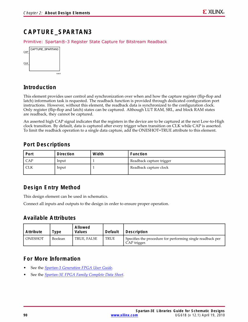
Chapter 2: About Design Elements
CAPTURE_SPARTAN3Primitive: Spartan®-3 Register State Capture for Bitstream Readback
IntroductionThis element provides user control and synchronization over when and how the capture register (flip-flop andlatch) information task is requested. The readback function is provided through dedicated configuration portinstructions. However, without this element, the readback data is synchronized to the configuration clock.Only register (flip-flop and latch) states can be captured. Although LUT RAM, SRL, and block RAM statesare readback, they cannot be captured.
An asserted high CAP signal indicates that the registers in the device are to be captured at the next Low-to-Highclock transition. By default, data is captured after every trigger when transition on CLK while CAP is asserted.To limit the readback operation to a single data capture, add the ONESHOT=TRUE attribute to this element.
Port DescriptionsPort Direction Width FunctionCAP Input 1 Readback capture trigger
CLK Input 1 Readback capture clock
Design Entry MethodThis design element can be used in schematics.
Connect all inputs and outputs to the design in order to ensure proper operation.
Available Attributes
Attribute TypeAllowedValues Default Description
ONESHOT Boolean TRUE, FALSE TRUE Specifies the procedure for performing single readback perCAP trigger.
For More Information• See the Spartan-3 Generation FPGA User Guide.
• See the Spartan-3E FPGA Family Complete Data Sheet.
Spartan-3E Libraries Guide for Schematic Designs90 www.xilinx.com UG618 (v 12.1) April 19, 2010
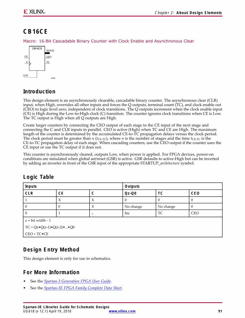
Chapter 2: About Design Elements
CB16CEMacro: 16-Bit Cascadable Binary Counter with Clock Enable and Asynchronous Clear
IntroductionThis design element is an asynchronously clearable, cascadable binary counter. The asynchronous clear (CLR)input, when High, overrides all other inputs and forces the Q outputs, terminal count (TC), and clock enable out(CEO) to logic level zero, independent of clock transitions. The Q outputs increment when the clock enable input(CE) is High during the Low-to-High clock (C) transition. The counter ignores clock transitions when CE is Low.The TC output is High when all Q outputs are High.
Create larger counters by connecting the CEO output of each stage to the CE input of the next stage andconnecting the C and CLR inputs in parallel. CEO is active (High) when TC and CE are High. The maximumlength of the counter is determined by the accumulated CE-to-TC propagation delays versus the clock period.The clock period must be greater than n (tCE-TC), where n is the number of stages and the time tCE-TC is theCE-to-TC propagation delay of each stage. When cascading counters, use the CEO output if the counter uses theCE input or use the TC output if it does not.
This counter is asynchronously cleared, outputs Low, when power is applied. For FPGA devices, power-onconditions are simulated when global set/reset (GSR) is active. GSR defaults to active-High but can be invertedby adding an inverter in front of the GSR input of the appropriate STARTUP_architecture symbol.
Logic TableInputs Outputs
CLR CE C Qz-Q0 TC CEO1 X X 0 0 0
0 0 X No change No change 0
0 1 ↑ Inc TC CEO
z = bit width - 1
TC = Qz•Q(z-1)•Q(z-2)•...•Q0
CEO = TC•CE
Design Entry MethodThis design element is only for use in schematics.
For More Information• See the Spartan-3 Generation FPGA User Guide.
• See the Spartan-3E FPGA Family Complete Data Sheet.
Spartan-3E Libraries Guide for Schematic DesignsUG618 (v 12.1) April 19, 2010 www.xilinx.com 91

Spartan-3E Libraries Guide for Schematic Designs92 www.xilinx.com UG618 (v 12.1) April 19, 2010
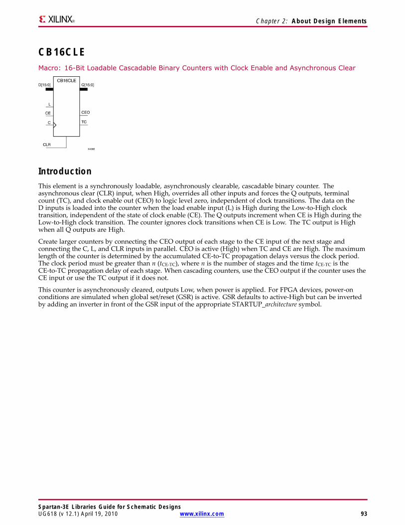
Chapter 2: About Design Elements
CB16CLEMacro: 16-Bit Loadable Cascadable Binary Counters with Clock Enable and Asynchronous Clear
IntroductionThis element is a synchronously loadable, asynchronously clearable, cascadable binary counter. Theasynchronous clear (CLR) input, when High, overrides all other inputs and forces the Q outputs, terminalcount (TC), and clock enable out (CEO) to logic level zero, independent of clock transitions. The data on theD inputs is loaded into the counter when the load enable input (L) is High during the Low-to-High clocktransition, independent of the state of clock enable (CE). The Q outputs increment when CE is High during theLow-to-High clock transition. The counter ignores clock transitions when CE is Low. The TC output is Highwhen all Q outputs are High.
Create larger counters by connecting the CEO output of each stage to the CE input of the next stage andconnecting the C, L, and CLR inputs in parallel. CEO is active (High) when TC and CE are High. The maximumlength of the counter is determined by the accumulated CE-to-TC propagation delays versus the clock period.The clock period must be greater than n (tCE-TC), where n is the number of stages and the time tCE-TC is theCE-to-TC propagation delay of each stage. When cascading counters, use the CEO output if the counter uses theCE input or use the TC output if it does not.
This counter is asynchronously cleared, outputs Low, when power is applied. For FPGA devices, power-onconditions are simulated when global set/reset (GSR) is active. GSR defaults to active-High but can be invertedby adding an inverter in front of the GSR input of the appropriate STARTUP_architecture symbol.
Spartan-3E Libraries Guide for Schematic DesignsUG618 (v 12.1) April 19, 2010 www.xilinx.com 93
Chapter 2: About Design Elements
Logic TableInputs Outputs
CLR L CE C Dz-D0 Qz-Q0 TC CEO1 X X X X 0 0 0
0 1 X ↑ Dn Dn TC CEO
0 0 0 X X No change No change 0
0 0 1 ↑ X Inc TC CEO
z = bit width - 1
TC = Qz•Q(z-1)•Q(z-2)•...•Q0
CEO = TC•CE
Design Entry MethodThis design element is only for use in schematics.
For More Information• See the Spartan-3 Generation FPGA User Guide.
• See the Spartan-3E FPGA Family Complete Data Sheet.
Spartan-3E Libraries Guide for Schematic Designs94 www.xilinx.com UG618 (v 12.1) April 19, 2010
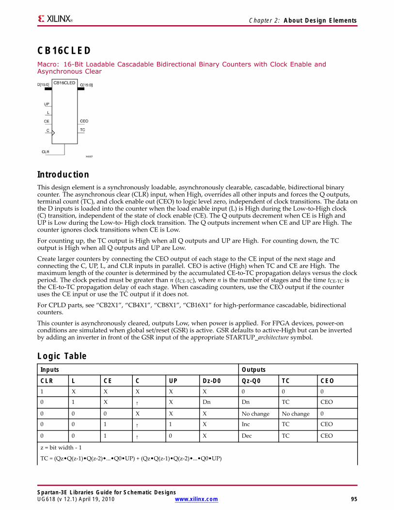
Chapter 2: About Design Elements
CB16CLEDMacro: 16-Bit Loadable Cascadable Bidirectional Binary Counters with Clock Enable andAsynchronous Clear
IntroductionThis design element is a synchronously loadable, asynchronously clearable, cascadable, bidirectional binarycounter. The asynchronous clear (CLR) input, when High, overrides all other inputs and forces the Q outputs,terminal count (TC), and clock enable out (CEO) to logic level zero, independent of clock transitions. The data onthe D inputs is loaded into the counter when the load enable input (L) is High during the Low-to-High clock(C) transition, independent of the state of clock enable (CE). The Q outputs decrement when CE is High andUP is Low during the Low-to- High clock transition. The Q outputs increment when CE and UP are High. Thecounter ignores clock transitions when CE is Low.
For counting up, the TC output is High when all Q outputs and UP are High. For counting down, the TCoutput is High when all Q outputs and UP are Low.
Create larger counters by connecting the CEO output of each stage to the CE input of the next stage andconnecting the C, UP, L, and CLR inputs in parallel. CEO is active (High) when TC and CE are High. Themaximum length of the counter is determined by the accumulated CE-to-TC propagation delays versus the clockperiod. The clock period must be greater than n (tCE-TC), where n is the number of stages and the time tCE-TC isthe CE-to-TC propagation delay of each stage. When cascading counters, use the CEO output if the counteruses the CE input or use the TC output if it does not.
For CPLD parts, see “CB2X1”, “CB4X1”, “CB8X1”, “CB16X1” for high-performance cascadable, bidirectionalcounters.
This counter is asynchronously cleared, outputs Low, when power is applied. For FPGA devices, power-onconditions are simulated when global set/reset (GSR) is active. GSR defaults to active-High but can be invertedby adding an inverter in front of the GSR input of the appropriate STARTUP_architecture symbol.
Logic TableInputs Outputs
CLR L CE C UP Dz-D0 Qz-Q0 TC CEO1 X X X X X 0 0 0
0 1 X ↑ X Dn Dn TC CEO
0 0 0 X X X No change No change 0
0 0 1 ↑ 1 X Inc TC CEO
0 0 1 ↑ 0 X Dec TC CEO
z = bit width - 1
TC = (Qz•Q(z-1)•Q(z-2)•...•Q0•UP) + (Qz•Q(z-1)•Q(z-2)•...•Q0•UP)
Spartan-3E Libraries Guide for Schematic DesignsUG618 (v 12.1) April 19, 2010 www.xilinx.com 95
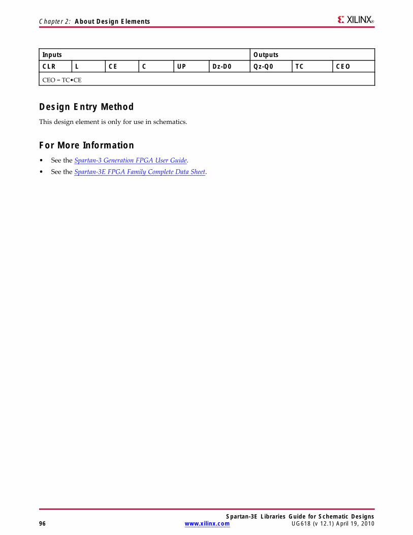
Chapter 2: About Design Elements
Inputs Outputs
CLR L CE C UP Dz-D0 Qz-Q0 TC CEO
CEO = TC•CE
Design Entry MethodThis design element is only for use in schematics.
For More Information• See the Spartan-3 Generation FPGA User Guide.
• See the Spartan-3E FPGA Family Complete Data Sheet.
Spartan-3E Libraries Guide for Schematic Designs96 www.xilinx.com UG618 (v 12.1) April 19, 2010
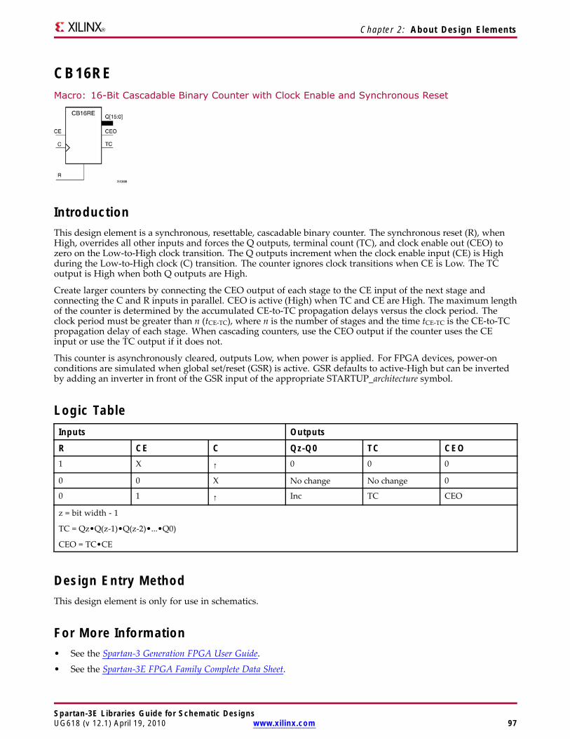
Chapter 2: About Design Elements
CB16REMacro: 16-Bit Cascadable Binary Counter with Clock Enable and Synchronous Reset
IntroductionThis design element is a synchronous, resettable, cascadable binary counter. The synchronous reset (R), whenHigh, overrides all other inputs and forces the Q outputs, terminal count (TC), and clock enable out (CEO) tozero on the Low-to-High clock transition. The Q outputs increment when the clock enable input (CE) is Highduring the Low-to-High clock (C) transition. The counter ignores clock transitions when CE is Low. The TCoutput is High when both Q outputs are High.
Create larger counters by connecting the CEO output of each stage to the CE input of the next stage andconnecting the C and R inputs in parallel. CEO is active (High) when TC and CE are High. The maximum lengthof the counter is determined by the accumulated CE-to-TC propagation delays versus the clock period. Theclock period must be greater than n (tCE-TC), where n is the number of stages and the time tCE-TC is the CE-to-TCpropagation delay of each stage. When cascading counters, use the CEO output if the counter uses the CEinput or use the TC output if it does not.
This counter is asynchronously cleared, outputs Low, when power is applied. For FPGA devices, power-onconditions are simulated when global set/reset (GSR) is active. GSR defaults to active-High but can be invertedby adding an inverter in front of the GSR input of the appropriate STARTUP_architecture symbol.
Logic TableInputs Outputs
R CE C Qz-Q0 TC CEO1 X ↑ 0 0 0
0 0 X No change No change 0
0 1 ↑ Inc TC CEO
z = bit width - 1
TC = Qz•Q(z-1)•Q(z-2)•...•Q0)
CEO = TC•CE
Design Entry MethodThis design element is only for use in schematics.
For More Information• See the Spartan-3 Generation FPGA User Guide.
• See the Spartan-3E FPGA Family Complete Data Sheet.
Spartan-3E Libraries Guide for Schematic DesignsUG618 (v 12.1) April 19, 2010 www.xilinx.com 97
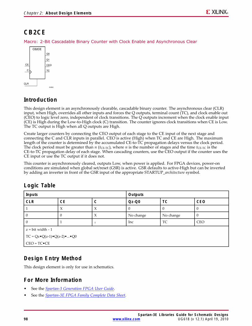
Chapter 2: About Design Elements
CB2CEMacro: 2-Bit Cascadable Binary Counter with Clock Enable and Asynchronous Clear
IntroductionThis design element is an asynchronously clearable, cascadable binary counter. The asynchronous clear (CLR)input, when High, overrides all other inputs and forces the Q outputs, terminal count (TC), and clock enable out(CEO) to logic level zero, independent of clock transitions. The Q outputs increment when the clock enable input(CE) is High during the Low-to-High clock (C) transition. The counter ignores clock transitions when CE is Low.The TC output is High when all Q outputs are High.
Create larger counters by connecting the CEO output of each stage to the CE input of the next stage andconnecting the C and CLR inputs in parallel. CEO is active (High) when TC and CE are High. The maximumlength of the counter is determined by the accumulated CE-to-TC propagation delays versus the clock period.The clock period must be greater than n (tCE-TC), where n is the number of stages and the time tCE-TC is theCE-to-TC propagation delay of each stage. When cascading counters, use the CEO output if the counter uses theCE input or use the TC output if it does not.
This counter is asynchronously cleared, outputs Low, when power is applied. For FPGA devices, power-onconditions are simulated when global set/reset (GSR) is active. GSR defaults to active-High but can be invertedby adding an inverter in front of the GSR input of the appropriate STARTUP_architecture symbol.
Logic TableInputs Outputs
CLR CE C Qz-Q0 TC CEO1 X X 0 0 0
0 0 X No change No change 0
0 1 ↑ Inc TC CEO
z = bit width - 1
TC = Qz•Q(z-1)•Q(z-2)•...•Q0
CEO = TC•CE
Design Entry MethodThis design element is only for use in schematics.
For More Information• See the Spartan-3 Generation FPGA User Guide.• See the Spartan-3E FPGA Family Complete Data Sheet.
Spartan-3E Libraries Guide for Schematic Designs98 www.xilinx.com UG618 (v 12.1) April 19, 2010
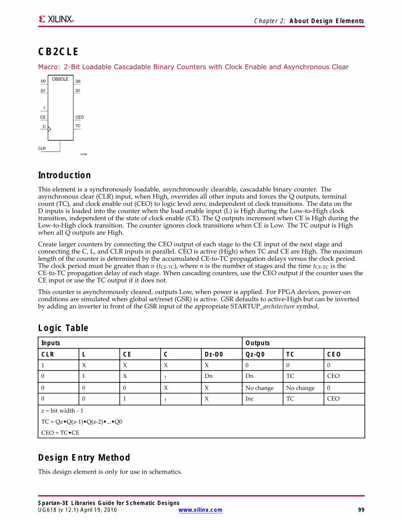
Chapter 2: About Design Elements
CB2CLEMacro: 2-Bit Loadable Cascadable Binary Counters with Clock Enable and Asynchronous Clear
IntroductionThis element is a synchronously loadable, asynchronously clearable, cascadable binary counter. Theasynchronous clear (CLR) input, when High, overrides all other inputs and forces the Q outputs, terminalcount (TC), and clock enable out (CEO) to logic level zero, independent of clock transitions. The data on theD inputs is loaded into the counter when the load enable input (L) is High during the Low-to-High clocktransition, independent of the state of clock enable (CE). The Q outputs increment when CE is High during theLow-to-High clock transition. The counter ignores clock transitions when CE is Low. The TC output is Highwhen all Q outputs are High.
Create larger counters by connecting the CEO output of each stage to the CE input of the next stage andconnecting the C, L, and CLR inputs in parallel. CEO is active (High) when TC and CE are High. The maximumlength of the counter is determined by the accumulated CE-to-TC propagation delays versus the clock period.The clock period must be greater than n (tCE-TC), where n is the number of stages and the time tCE-TC is theCE-to-TC propagation delay of each stage. When cascading counters, use the CEO output if the counter uses theCE input or use the TC output if it does not.
This counter is asynchronously cleared, outputs Low, when power is applied. For FPGA devices, power-onconditions are simulated when global set/reset (GSR) is active. GSR defaults to active-High but can be invertedby adding an inverter in front of the GSR input of the appropriate STARTUP_architecture symbol.
Logic TableInputs Outputs
CLR L CE C Dz-D0 Qz-Q0 TC CEO1 X X X X 0 0 0
0 1 X ↑ Dn Dn TC CEO
0 0 0 X X No change No change 0
0 0 1 ↑ X Inc TC CEO
z = bit width - 1
TC = Qz•Q(z-1)•Q(z-2)•...•Q0
CEO = TC•CE
Design Entry MethodThis design element is only for use in schematics.
Spartan-3E Libraries Guide for Schematic DesignsUG618 (v 12.1) April 19, 2010 www.xilinx.com 99

Chapter 2: About Design Elements
For More Information• See the Spartan-3 Generation FPGA User Guide.
• See the Spartan-3E FPGA Family Complete Data Sheet.
Spartan-3E Libraries Guide for Schematic Designs100 www.xilinx.com UG618 (v 12.1) April 19, 2010
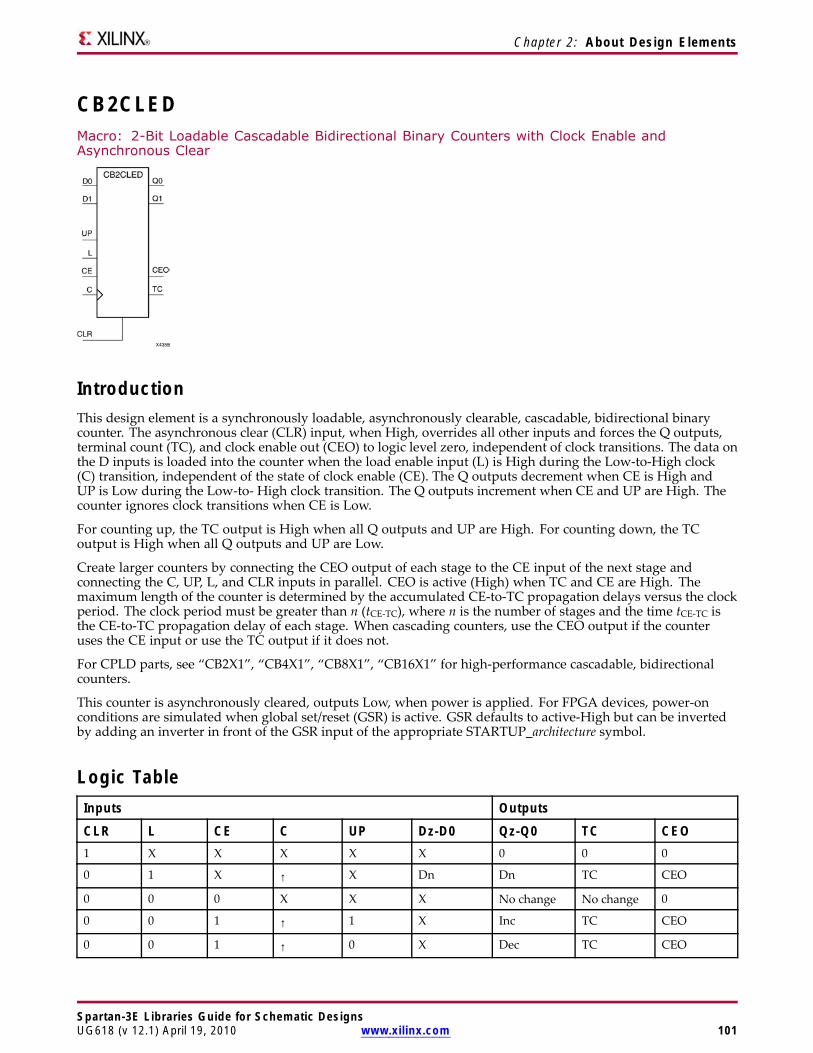
Chapter 2: About Design Elements
CB2CLEDMacro: 2-Bit Loadable Cascadable Bidirectional Binary Counters with Clock Enable andAsynchronous Clear
IntroductionThis design element is a synchronously loadable, asynchronously clearable, cascadable, bidirectional binarycounter. The asynchronous clear (CLR) input, when High, overrides all other inputs and forces the Q outputs,terminal count (TC), and clock enable out (CEO) to logic level zero, independent of clock transitions. The data onthe D inputs is loaded into the counter when the load enable input (L) is High during the Low-to-High clock(C) transition, independent of the state of clock enable (CE). The Q outputs decrement when CE is High andUP is Low during the Low-to- High clock transition. The Q outputs increment when CE and UP are High. Thecounter ignores clock transitions when CE is Low.
For counting up, the TC output is High when all Q outputs and UP are High. For counting down, the TCoutput is High when all Q outputs and UP are Low.
Create larger counters by connecting the CEO output of each stage to the CE input of the next stage andconnecting the C, UP, L, and CLR inputs in parallel. CEO is active (High) when TC and CE are High. Themaximum length of the counter is determined by the accumulated CE-to-TC propagation delays versus the clockperiod. The clock period must be greater than n (tCE-TC), where n is the number of stages and the time tCE-TC isthe CE-to-TC propagation delay of each stage. When cascading counters, use the CEO output if the counteruses the CE input or use the TC output if it does not.
For CPLD parts, see “CB2X1”, “CB4X1”, “CB8X1”, “CB16X1” for high-performance cascadable, bidirectionalcounters.
This counter is asynchronously cleared, outputs Low, when power is applied. For FPGA devices, power-onconditions are simulated when global set/reset (GSR) is active. GSR defaults to active-High but can be invertedby adding an inverter in front of the GSR input of the appropriate STARTUP_architecture symbol.
Logic TableInputs Outputs
CLR L CE C UP Dz-D0 Qz-Q0 TC CEO1 X X X X X 0 0 0
0 1 X ↑ X Dn Dn TC CEO
0 0 0 X X X No change No change 0
0 0 1 ↑ 1 X Inc TC CEO
0 0 1 ↑ 0 X Dec TC CEO
Spartan-3E Libraries Guide for Schematic DesignsUG618 (v 12.1) April 19, 2010 www.xilinx.com 101
Chapter 2: About Design Elements
Inputs Outputs
CLR L CE C UP Dz-D0 Qz-Q0 TC CEOz = bit width - 1
TC = (Qz•Q(z-1)•Q(z-2)•...•Q0•UP) + (Qz•Q(z-1)•Q(z-2)•...•Q0•UP)
CEO = TC•CE
Design Entry MethodThis design element is only for use in schematics.
For More Information• See the Spartan-3 Generation FPGA User Guide.
• See the Spartan-3E FPGA Family Complete Data Sheet.
Spartan-3E Libraries Guide for Schematic Designs102 www.xilinx.com UG618 (v 12.1) April 19, 2010
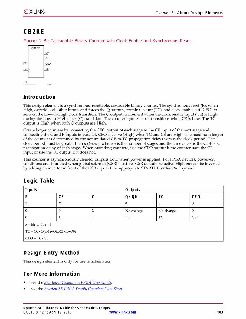
Chapter 2: About Design Elements
CB2REMacro: 2-Bit Cascadable Binary Counter with Clock Enable and Synchronous Reset
IntroductionThis design element is a synchronous, resettable, cascadable binary counter. The synchronous reset (R), whenHigh, overrides all other inputs and forces the Q outputs, terminal count (TC), and clock enable out (CEO) tozero on the Low-to-High clock transition. The Q outputs increment when the clock enable input (CE) is Highduring the Low-to-High clock (C) transition. The counter ignores clock transitions when CE is Low. The TCoutput is High when both Q outputs are High.
Create larger counters by connecting the CEO output of each stage to the CE input of the next stage andconnecting the C and R inputs in parallel. CEO is active (High) when TC and CE are High. The maximum lengthof the counter is determined by the accumulated CE-to-TC propagation delays versus the clock period. Theclock period must be greater than n (tCE-TC), where n is the number of stages and the time tCE-TC is the CE-to-TCpropagation delay of each stage. When cascading counters, use the CEO output if the counter uses the CEinput or use the TC output if it does not.
This counter is asynchronously cleared, outputs Low, when power is applied. For FPGA devices, power-onconditions are simulated when global set/reset (GSR) is active. GSR defaults to active-High but can be invertedby adding an inverter in front of the GSR input of the appropriate STARTUP_architecture symbol.
Logic TableInputs Outputs
R CE C Qz-Q0 TC CEO1 X ↑ 0 0 0
0 0 X No change No change 0
0 1 ↑ Inc TC CEO
z = bit width - 1
TC = Qz•Q(z-1)•Q(z-2)•...•Q0)
CEO = TC•CE
Design Entry MethodThis design element is only for use in schematics.
For More Information• See the Spartan-3 Generation FPGA User Guide.• See the Spartan-3E FPGA Family Complete Data Sheet.
Spartan-3E Libraries Guide for Schematic DesignsUG618 (v 12.1) April 19, 2010 www.xilinx.com 103
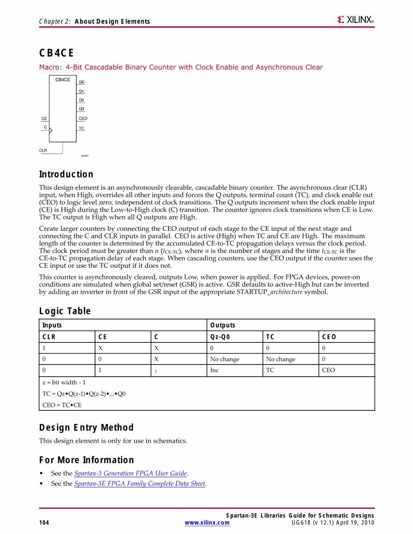
Chapter 2: About Design Elements
CB4CEMacro: 4-Bit Cascadable Binary Counter with Clock Enable and Asynchronous Clear
IntroductionThis design element is an asynchronously clearable, cascadable binary counter. The asynchronous clear (CLR)input, when High, overrides all other inputs and forces the Q outputs, terminal count (TC), and clock enable out(CEO) to logic level zero, independent of clock transitions. The Q outputs increment when the clock enable input(CE) is High during the Low-to-High clock (C) transition. The counter ignores clock transitions when CE is Low.The TC output is High when all Q outputs are High.
Create larger counters by connecting the CEO output of each stage to the CE input of the next stage andconnecting the C and CLR inputs in parallel. CEO is active (High) when TC and CE are High. The maximumlength of the counter is determined by the accumulated CE-to-TC propagation delays versus the clock period.The clock period must be greater than n (tCE-TC), where n is the number of stages and the time tCE-TC is theCE-to-TC propagation delay of each stage. When cascading counters, use the CEO output if the counter uses theCE input or use the TC output if it does not.
This counter is asynchronously cleared, outputs Low, when power is applied. For FPGA devices, power-onconditions are simulated when global set/reset (GSR) is active. GSR defaults to active-High but can be invertedby adding an inverter in front of the GSR input of the appropriate STARTUP_architecture symbol.
Logic TableInputs Outputs
CLR CE C Qz-Q0 TC CEO1 X X 0 0 0
0 0 X No change No change 0
0 1 ↑ Inc TC CEO
z = bit width - 1
TC = Qz•Q(z-1)•Q(z-2)•...•Q0
CEO = TC•CE
Design Entry MethodThis design element is only for use in schematics.
For More Information• See the Spartan-3 Generation FPGA User Guide.• See the Spartan-3E FPGA Family Complete Data Sheet.
Spartan-3E Libraries Guide for Schematic Designs104 www.xilinx.com UG618 (v 12.1) April 19, 2010
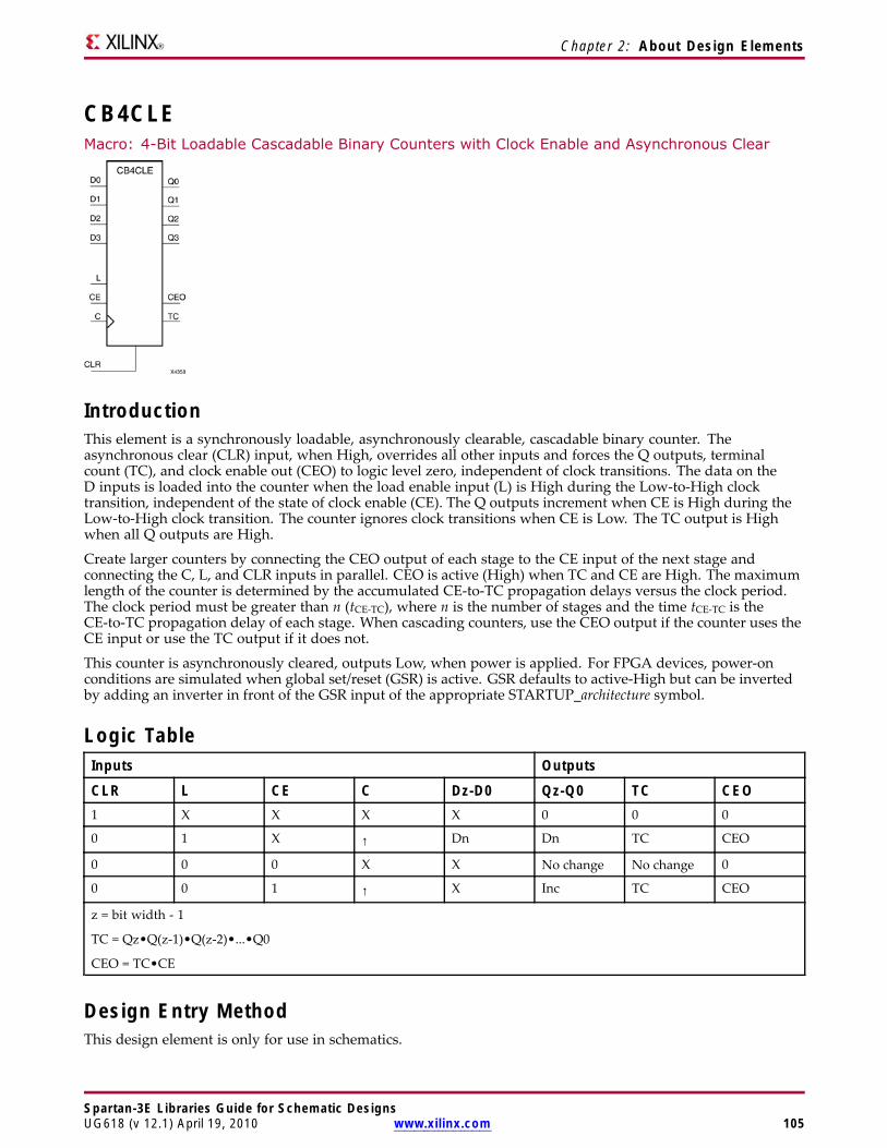
Chapter 2: About Design Elements
CB4CLEMacro: 4-Bit Loadable Cascadable Binary Counters with Clock Enable and Asynchronous Clear
IntroductionThis element is a synchronously loadable, asynchronously clearable, cascadable binary counter. Theasynchronous clear (CLR) input, when High, overrides all other inputs and forces the Q outputs, terminalcount (TC), and clock enable out (CEO) to logic level zero, independent of clock transitions. The data on theD inputs is loaded into the counter when the load enable input (L) is High during the Low-to-High clocktransition, independent of the state of clock enable (CE). The Q outputs increment when CE is High during theLow-to-High clock transition. The counter ignores clock transitions when CE is Low. The TC output is Highwhen all Q outputs are High.
Create larger counters by connecting the CEO output of each stage to the CE input of the next stage andconnecting the C, L, and CLR inputs in parallel. CEO is active (High) when TC and CE are High. The maximumlength of the counter is determined by the accumulated CE-to-TC propagation delays versus the clock period.The clock period must be greater than n (tCE-TC), where n is the number of stages and the time tCE-TC is theCE-to-TC propagation delay of each stage. When cascading counters, use the CEO output if the counter uses theCE input or use the TC output if it does not.
This counter is asynchronously cleared, outputs Low, when power is applied. For FPGA devices, power-onconditions are simulated when global set/reset (GSR) is active. GSR defaults to active-High but can be invertedby adding an inverter in front of the GSR input of the appropriate STARTUP_architecture symbol.
Logic TableInputs Outputs
CLR L CE C Dz-D0 Qz-Q0 TC CEO1 X X X X 0 0 0
0 1 X ↑ Dn Dn TC CEO
0 0 0 X X No change No change 0
0 0 1 ↑ X Inc TC CEO
z = bit width - 1
TC = Qz•Q(z-1)•Q(z-2)•...•Q0
CEO = TC•CE
Design Entry MethodThis design element is only for use in schematics.
Spartan-3E Libraries Guide for Schematic DesignsUG618 (v 12.1) April 19, 2010 www.xilinx.com 105

Chapter 2: About Design Elements
For More Information• See the Spartan-3 Generation FPGA User Guide.
• See the Spartan-3E FPGA Family Complete Data Sheet.
Spartan-3E Libraries Guide for Schematic Designs106 www.xilinx.com UG618 (v 12.1) April 19, 2010
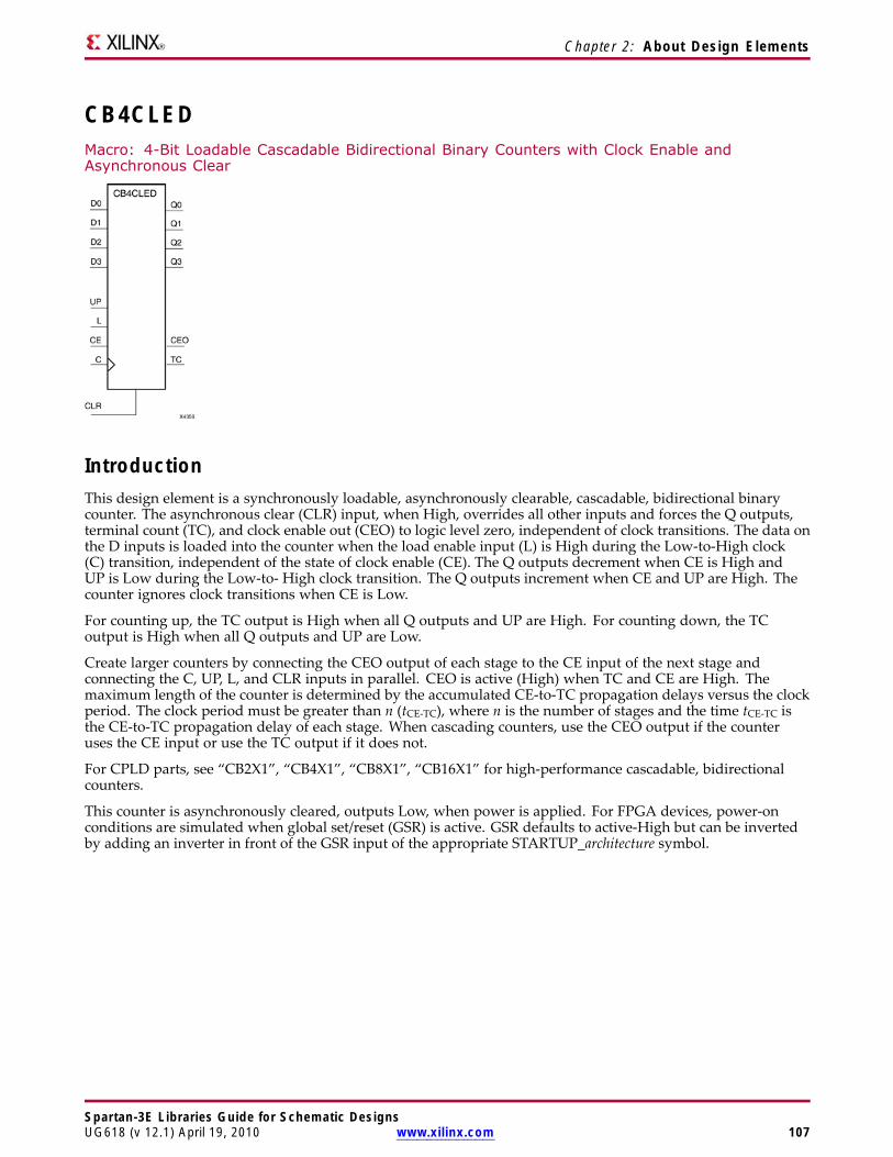
Chapter 2: About Design Elements
CB4CLEDMacro: 4-Bit Loadable Cascadable Bidirectional Binary Counters with Clock Enable andAsynchronous Clear
IntroductionThis design element is a synchronously loadable, asynchronously clearable, cascadable, bidirectional binarycounter. The asynchronous clear (CLR) input, when High, overrides all other inputs and forces the Q outputs,terminal count (TC), and clock enable out (CEO) to logic level zero, independent of clock transitions. The data onthe D inputs is loaded into the counter when the load enable input (L) is High during the Low-to-High clock(C) transition, independent of the state of clock enable (CE). The Q outputs decrement when CE is High andUP is Low during the Low-to- High clock transition. The Q outputs increment when CE and UP are High. Thecounter ignores clock transitions when CE is Low.
For counting up, the TC output is High when all Q outputs and UP are High. For counting down, the TCoutput is High when all Q outputs and UP are Low.
Create larger counters by connecting the CEO output of each stage to the CE input of the next stage andconnecting the C, UP, L, and CLR inputs in parallel. CEO is active (High) when TC and CE are High. Themaximum length of the counter is determined by the accumulated CE-to-TC propagation delays versus the clockperiod. The clock period must be greater than n (tCE-TC), where n is the number of stages and the time tCE-TC isthe CE-to-TC propagation delay of each stage. When cascading counters, use the CEO output if the counteruses the CE input or use the TC output if it does not.
For CPLD parts, see “CB2X1”, “CB4X1”, “CB8X1”, “CB16X1” for high-performance cascadable, bidirectionalcounters.
This counter is asynchronously cleared, outputs Low, when power is applied. For FPGA devices, power-onconditions are simulated when global set/reset (GSR) is active. GSR defaults to active-High but can be invertedby adding an inverter in front of the GSR input of the appropriate STARTUP_architecture symbol.
Spartan-3E Libraries Guide for Schematic DesignsUG618 (v 12.1) April 19, 2010 www.xilinx.com 107
Chapter 2: About Design Elements
Logic TableInputs Outputs
CLR L CE C UP Dz-D0 Qz-Q0 TC CEO1 X X X X X 0 0 0
0 1 X ↑ X Dn Dn TC CEO
0 0 0 X X X No change No change 0
0 0 1 ↑ 1 X Inc TC CEO
0 0 1 ↑ 0 X Dec TC CEO
z = bit width - 1
TC = (Qz•Q(z-1)•Q(z-2)•...•Q0•UP) + (Qz•Q(z-1)•Q(z-2)•...•Q0•UP)
CEO = TC•CE
Design Entry MethodThis design element is only for use in schematics.
For More Information• See the Spartan-3 Generation FPGA User Guide.
• See the Spartan-3E FPGA Family Complete Data Sheet.
Spartan-3E Libraries Guide for Schematic Designs108 www.xilinx.com UG618 (v 12.1) April 19, 2010
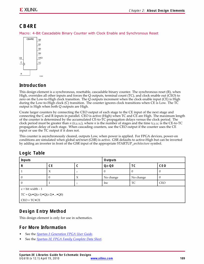
Chapter 2: About Design Elements
CB4REMacro: 4-Bit Cascadable Binary Counter with Clock Enable and Synchronous Reset
IntroductionThis design element is a synchronous, resettable, cascadable binary counter. The synchronous reset (R), whenHigh, overrides all other inputs and forces the Q outputs, terminal count (TC), and clock enable out (CEO) tozero on the Low-to-High clock transition. The Q outputs increment when the clock enable input (CE) is Highduring the Low-to-High clock (C) transition. The counter ignores clock transitions when CE is Low. The TCoutput is High when both Q outputs are High.
Create larger counters by connecting the CEO output of each stage to the CE input of the next stage andconnecting the C and R inputs in parallel. CEO is active (High) when TC and CE are High. The maximum lengthof the counter is determined by the accumulated CE-to-TC propagation delays versus the clock period. Theclock period must be greater than n (tCE-TC), where n is the number of stages and the time tCE-TC is the CE-to-TCpropagation delay of each stage. When cascading counters, use the CEO output if the counter uses the CEinput or use the TC output if it does not.
This counter is asynchronously cleared, outputs Low, when power is applied. For FPGA devices, power-onconditions are simulated when global set/reset (GSR) is active. GSR defaults to active-High but can be invertedby adding an inverter in front of the GSR input of the appropriate STARTUP_architecture symbol.
Logic TableInputs Outputs
R CE C Qz-Q0 TC CEO1 X ↑ 0 0 0
0 0 X No change No change 0
0 1 ↑ Inc TC CEO
z = bit width - 1
TC = Qz•Q(z-1)•Q(z-2)•...•Q0)
CEO = TC•CE
Design Entry MethodThis design element is only for use in schematics.
For More Information• See the Spartan-3 Generation FPGA User Guide.• See the Spartan-3E FPGA Family Complete Data Sheet.
Spartan-3E Libraries Guide for Schematic DesignsUG618 (v 12.1) April 19, 2010 www.xilinx.com 109
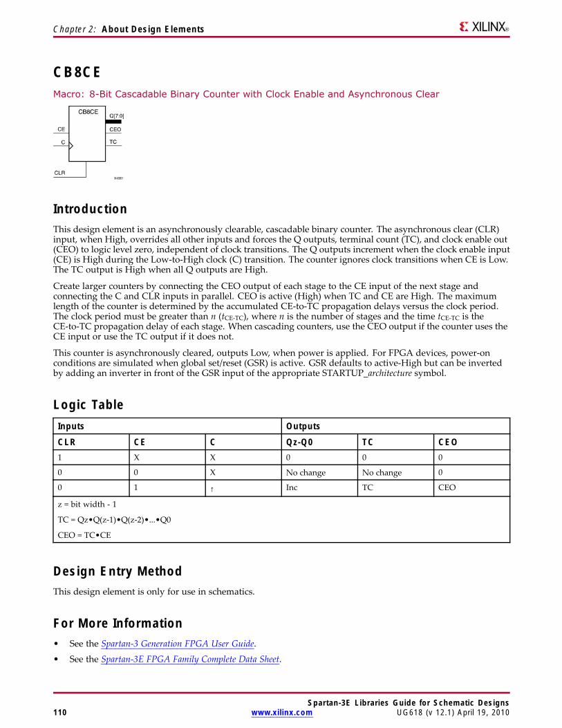
Chapter 2: About Design Elements
CB8CEMacro: 8-Bit Cascadable Binary Counter with Clock Enable and Asynchronous Clear
IntroductionThis design element is an asynchronously clearable, cascadable binary counter. The asynchronous clear (CLR)input, when High, overrides all other inputs and forces the Q outputs, terminal count (TC), and clock enable out(CEO) to logic level zero, independent of clock transitions. The Q outputs increment when the clock enable input(CE) is High during the Low-to-High clock (C) transition. The counter ignores clock transitions when CE is Low.The TC output is High when all Q outputs are High.
Create larger counters by connecting the CEO output of each stage to the CE input of the next stage andconnecting the C and CLR inputs in parallel. CEO is active (High) when TC and CE are High. The maximumlength of the counter is determined by the accumulated CE-to-TC propagation delays versus the clock period.The clock period must be greater than n (tCE-TC), where n is the number of stages and the time tCE-TC is theCE-to-TC propagation delay of each stage. When cascading counters, use the CEO output if the counter uses theCE input or use the TC output if it does not.
This counter is asynchronously cleared, outputs Low, when power is applied. For FPGA devices, power-onconditions are simulated when global set/reset (GSR) is active. GSR defaults to active-High but can be invertedby adding an inverter in front of the GSR input of the appropriate STARTUP_architecture symbol.
Logic TableInputs Outputs
CLR CE C Qz-Q0 TC CEO1 X X 0 0 0
0 0 X No change No change 0
0 1 ↑ Inc TC CEO
z = bit width - 1
TC = Qz•Q(z-1)•Q(z-2)•...•Q0
CEO = TC•CE
Design Entry MethodThis design element is only for use in schematics.
For More Information• See the Spartan-3 Generation FPGA User Guide.
• See the Spartan-3E FPGA Family Complete Data Sheet.
Spartan-3E Libraries Guide for Schematic Designs110 www.xilinx.com UG618 (v 12.1) April 19, 2010

Spartan-3E Libraries Guide for Schematic Designs111 www.xilinx.com UG618 (v 12.1) April 19, 2010
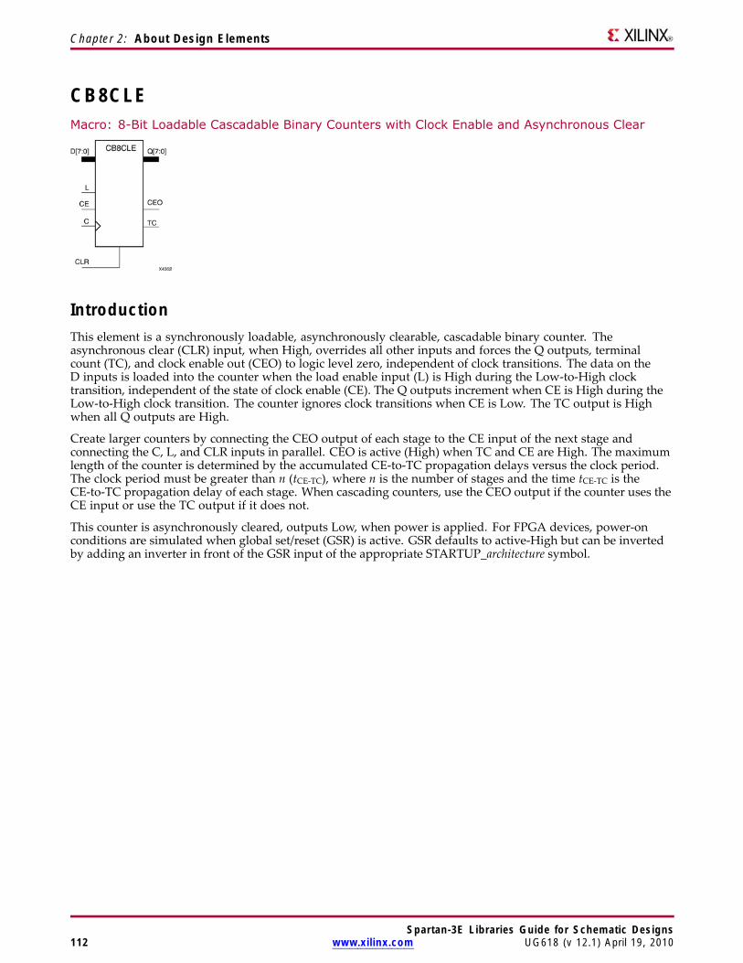
Chapter 2: About Design Elements
CB8CLEMacro: 8-Bit Loadable Cascadable Binary Counters with Clock Enable and Asynchronous Clear
IntroductionThis element is a synchronously loadable, asynchronously clearable, cascadable binary counter. Theasynchronous clear (CLR) input, when High, overrides all other inputs and forces the Q outputs, terminalcount (TC), and clock enable out (CEO) to logic level zero, independent of clock transitions. The data on theD inputs is loaded into the counter when the load enable input (L) is High during the Low-to-High clocktransition, independent of the state of clock enable (CE). The Q outputs increment when CE is High during theLow-to-High clock transition. The counter ignores clock transitions when CE is Low. The TC output is Highwhen all Q outputs are High.
Create larger counters by connecting the CEO output of each stage to the CE input of the next stage andconnecting the C, L, and CLR inputs in parallel. CEO is active (High) when TC and CE are High. The maximumlength of the counter is determined by the accumulated CE-to-TC propagation delays versus the clock period.The clock period must be greater than n (tCE-TC), where n is the number of stages and the time tCE-TC is theCE-to-TC propagation delay of each stage. When cascading counters, use the CEO output if the counter uses theCE input or use the TC output if it does not.
This counter is asynchronously cleared, outputs Low, when power is applied. For FPGA devices, power-onconditions are simulated when global set/reset (GSR) is active. GSR defaults to active-High but can be invertedby adding an inverter in front of the GSR input of the appropriate STARTUP_architecture symbol.
Spartan-3E Libraries Guide for Schematic Designs112 www.xilinx.com UG618 (v 12.1) April 19, 2010
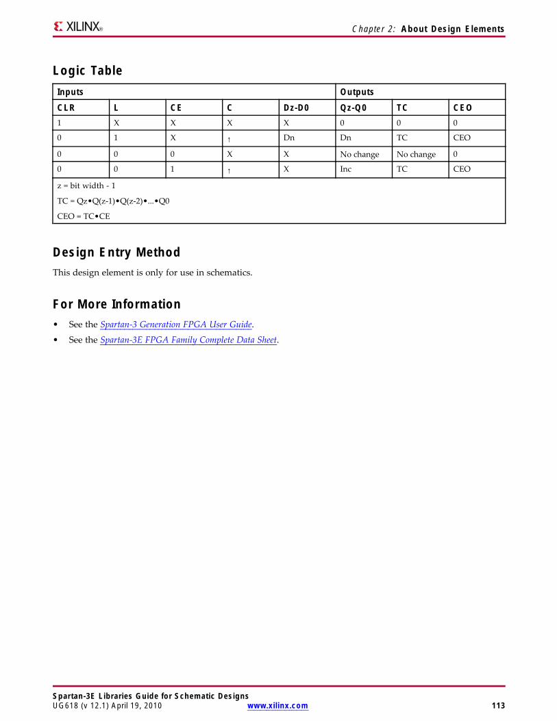
Chapter 2: About Design Elements
Logic TableInputs Outputs
CLR L CE C Dz-D0 Qz-Q0 TC CEO1 X X X X 0 0 0
0 1 X ↑ Dn Dn TC CEO
0 0 0 X X No change No change 0
0 0 1 ↑ X Inc TC CEO
z = bit width - 1
TC = Qz•Q(z-1)•Q(z-2)•...•Q0
CEO = TC•CE
Design Entry MethodThis design element is only for use in schematics.
For More Information• See the Spartan-3 Generation FPGA User Guide.
• See the Spartan-3E FPGA Family Complete Data Sheet.
Spartan-3E Libraries Guide for Schematic DesignsUG618 (v 12.1) April 19, 2010 www.xilinx.com 113
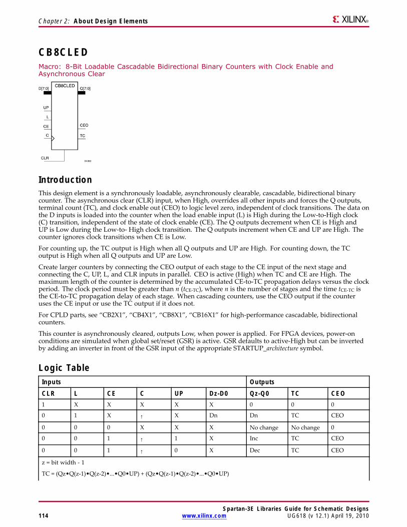
Chapter 2: About Design Elements
CB8CLEDMacro: 8-Bit Loadable Cascadable Bidirectional Binary Counters with Clock Enable andAsynchronous Clear
IntroductionThis design element is a synchronously loadable, asynchronously clearable, cascadable, bidirectional binarycounter. The asynchronous clear (CLR) input, when High, overrides all other inputs and forces the Q outputs,terminal count (TC), and clock enable out (CEO) to logic level zero, independent of clock transitions. The data onthe D inputs is loaded into the counter when the load enable input (L) is High during the Low-to-High clock(C) transition, independent of the state of clock enable (CE). The Q outputs decrement when CE is High andUP is Low during the Low-to- High clock transition. The Q outputs increment when CE and UP are High. Thecounter ignores clock transitions when CE is Low.
For counting up, the TC output is High when all Q outputs and UP are High. For counting down, the TCoutput is High when all Q outputs and UP are Low.
Create larger counters by connecting the CEO output of each stage to the CE input of the next stage andconnecting the C, UP, L, and CLR inputs in parallel. CEO is active (High) when TC and CE are High. Themaximum length of the counter is determined by the accumulated CE-to-TC propagation delays versus the clockperiod. The clock period must be greater than n (tCE-TC), where n is the number of stages and the time tCE-TC isthe CE-to-TC propagation delay of each stage. When cascading counters, use the CEO output if the counteruses the CE input or use the TC output if it does not.
For CPLD parts, see “CB2X1”, “CB4X1”, “CB8X1”, “CB16X1” for high-performance cascadable, bidirectionalcounters.
This counter is asynchronously cleared, outputs Low, when power is applied. For FPGA devices, power-onconditions are simulated when global set/reset (GSR) is active. GSR defaults to active-High but can be invertedby adding an inverter in front of the GSR input of the appropriate STARTUP_architecture symbol.
Logic TableInputs Outputs
CLR L CE C UP Dz-D0 Qz-Q0 TC CEO1 X X X X X 0 0 0
0 1 X ↑ X Dn Dn TC CEO
0 0 0 X X X No change No change 0
0 0 1 ↑ 1 X Inc TC CEO
0 0 1 ↑ 0 X Dec TC CEO
z = bit width - 1
TC = (Qz•Q(z-1)•Q(z-2)•...•Q0•UP) + (Qz•Q(z-1)•Q(z-2)•...•Q0•UP)
Spartan-3E Libraries Guide for Schematic Designs114 www.xilinx.com UG618 (v 12.1) April 19, 2010
Chapter 2: About Design Elements
Inputs Outputs
CLR L CE C UP Dz-D0 Qz-Q0 TC CEO
CEO = TC•CE
Design Entry MethodThis design element is only for use in schematics.
For More Information• See the Spartan-3 Generation FPGA User Guide.
• See the Spartan-3E FPGA Family Complete Data Sheet.
Spartan-3E Libraries Guide for Schematic DesignsUG618 (v 12.1) April 19, 2010 www.xilinx.com 115
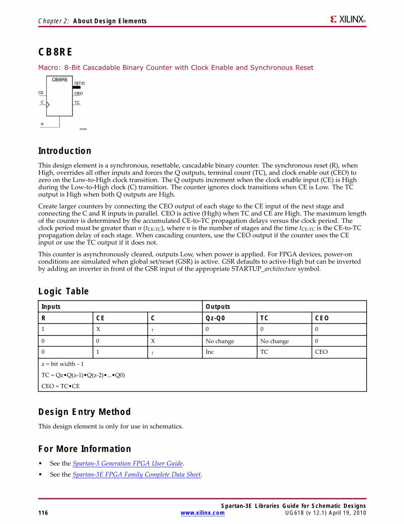
Chapter 2: About Design Elements
CB8REMacro: 8-Bit Cascadable Binary Counter with Clock Enable and Synchronous Reset
IntroductionThis design element is a synchronous, resettable, cascadable binary counter. The synchronous reset (R), whenHigh, overrides all other inputs and forces the Q outputs, terminal count (TC), and clock enable out (CEO) tozero on the Low-to-High clock transition. The Q outputs increment when the clock enable input (CE) is Highduring the Low-to-High clock (C) transition. The counter ignores clock transitions when CE is Low. The TCoutput is High when both Q outputs are High.
Create larger counters by connecting the CEO output of each stage to the CE input of the next stage andconnecting the C and R inputs in parallel. CEO is active (High) when TC and CE are High. The maximum lengthof the counter is determined by the accumulated CE-to-TC propagation delays versus the clock period. Theclock period must be greater than n (tCE-TC), where n is the number of stages and the time tCE-TC is the CE-to-TCpropagation delay of each stage. When cascading counters, use the CEO output if the counter uses the CEinput or use the TC output if it does not.
This counter is asynchronously cleared, outputs Low, when power is applied. For FPGA devices, power-onconditions are simulated when global set/reset (GSR) is active. GSR defaults to active-High but can be invertedby adding an inverter in front of the GSR input of the appropriate STARTUP_architecture symbol.
Logic TableInputs Outputs
R CE C Qz-Q0 TC CEO1 X ↑ 0 0 0
0 0 X No change No change 0
0 1 ↑ Inc TC CEO
z = bit width - 1
TC = Qz•Q(z-1)•Q(z-2)•...•Q0)
CEO = TC•CE
Design Entry MethodThis design element is only for use in schematics.
For More Information• See the Spartan-3 Generation FPGA User Guide.• See the Spartan-3E FPGA Family Complete Data Sheet.
Spartan-3E Libraries Guide for Schematic Designs116 www.xilinx.com UG618 (v 12.1) April 19, 2010
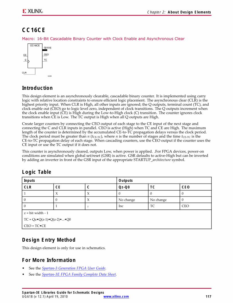
Chapter 2: About Design Elements
CC16CEMacro: 16-Bit Cascadable Binary Counter with Clock Enable and Asynchronous Clear
IntroductionThis design element is an asynchronously clearable, cascadable binary counter. It is implemented using carrylogic with relative location constraints to ensure efficient logic placement. The asynchronous clear (CLR) is thehighest priority input. When CLR is High, all other inputs are ignored; the Q outputs, terminal count (TC), andclock enable out (CEO) go to logic level zero, independent of clock transitions. The Q outputs increment whenthe clock enable input (CE) is High during the Low-to-High clock (C) transition. The counter ignores clocktransitions when CE is Low. The TC output is High when all Q outputs are High.
Create larger counters by connecting the CEO output of each stage to the CE input of the next stage andconnecting the C and CLR inputs in parallel. CEO is active (High) when TC and CE are High. The maximumlength of the counter is determined by the accumulated CE-to-TC propagation delays versus the clock period.The clock period must be greater than n (tCE-TC), where n is the number of stages and the time tCE-TC is theCE-to-TC propagation delay of each stage. When cascading counters, use the CEO output if the counter uses theCE input or use the TC output if it does not.
This counter is asynchronously cleared, outputs Low, when power is applied. .For FPGA devices, power-onconditions are simulated when global set/reset (GSR) is active. GSR defaults to active-High but can be invertedby adding an inverter in front of the GSR input of the appropriate STARTUP_architecture symbol.
Logic TableInputs Outputs
CLR CE C Qz-Q0 TC CEO1 X X 0 0 0
0 0 X No change No change 0
0 1 ↑ Inc TC CEO
z = bit width - 1
TC = Qz•Q(z-1)•Q(z-2)•...•Q0
CEO = TC•CE
Design Entry MethodThis design element is only for use in schematics.
For More Information• See the Spartan-3 Generation FPGA User Guide.• See the Spartan-3E FPGA Family Complete Data Sheet.
Spartan-3E Libraries Guide for Schematic DesignsUG618 (v 12.1) April 19, 2010 www.xilinx.com 117
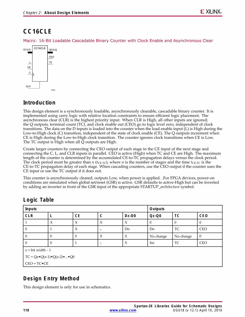
Chapter 2: About Design Elements
CC16CLEMacro: 16-Bit Loadable Cascadable Binary Counter with Clock Enable and Asynchronous Clear
IntroductionThis design element is a synchronously loadable, asynchronously clearable, cascadable binary counter. It isimplemented using carry logic with relative location constraints to ensure efficient logic placement. Theasynchronous clear (CLR) is the highest priority input. When CLR is High, all other inputs are ignored;the Q outputs, terminal count (TC), and clock enable out (CEO) go to logic level zero, independent of clocktransitions. The data on the D inputs is loaded into the counter when the load enable input (L) is High during theLow-to-High clock (C) transition, independent of the state of clock enable (CE). The Q outputs increment whenCE is High during the Low-to-High clock transition. The counter ignores clock transitions when CE is Low.The TC output is High when all Q outputs are High.
Create larger counters by connecting the CEO output of each stage to the CE input of the next stage andconnecting the C, L, and CLR inputs in parallel. CEO is active (High) when TC and CE are High. The maximumlength of the counter is determined by the accumulated CE-to-TC propagation delays versus the clock period.The clock period must be greater than n (tCE-TC), where n is the number of stages and the time tCE-TC is theCE-to-TC propagation delay of each stage. When cascading counters, use the CEO output if the counter uses theCE input or use the TC output if it does not.
This counter is asynchronously cleared, outputs Low, when power is applied. .For FPGA devices, power-onconditions are simulated when global set/reset (GSR) is active. GSR defaults to active-High but can be invertedby adding an inverter in front of the GSR input of the appropriate STARTUP_architecture symbol.
Logic TableInputs Outputs
CLR L CE C Dz-D0 Qz-Q0 TC CEO1 X X X X 0 0 0
0 1 X ↑ Dn Dn TC CEO
0 0 0 X X No change No change 0
0 0 1 ↑ X Inc TC CEO
z = bit width - 1
TC = Qz•Q(z-1)•Q(z-2)•...•Q0
CEO = TC•CE
Design Entry MethodThis design element is only for use in schematics.
Spartan-3E Libraries Guide for Schematic Designs118 www.xilinx.com UG618 (v 12.1) April 19, 2010

Chapter 2: About Design Elements
For More Information• See the Spartan-3 Generation FPGA User Guide.
• See the Spartan-3E FPGA Family Complete Data Sheet.
Spartan-3E Libraries Guide for Schematic DesignsUG618 (v 12.1) April 19, 2010 www.xilinx.com 119

Chapter 2: About Design Elements
CC16CLEDMacro: 16-Bit Loadable Cascadable Bidirectional Binary Counter with Clock Enable andAsynchronous Clear
IntroductionThis design element is a synchronously loadable, asynchronously clearable, cascadable, bidirectional binarycounter. It is implemented using carry logic with relative location constraints, which assures most efficient logicplacement. The asynchronous clear (CLR) is the highest priority input. When CLR is High, all other inputs areignored; the Q outputs, terminal count (TC), and clock enable out (CEO) go to logic level zero, independent ofclock transitions. The data on the D inputs is loaded into the counter when the load enable input (L) is Highduring the Low-to-High clock (C) transition, independent of the state of clock enable (CE). The Q outputsdecrement when CE is High and UP is Low during the Low-to-High clock transition. The Q outputs incrementwhen CE and UP are High. The counter ignores clock transitions when CE is Low.
For counting up, the TC output is High when all Q outputs and UP are High. For counting down, the TCoutput is High when all Q outputs and UP are Low.
Create larger counters by connecting the CEO output of each stage to the CE input of the next stage andconnecting the C, UP, L, and CLR inputs in parallel. CEO is active (High) when TC and CE are High. Themaximum length of the counter is determined by the accumulated CE-to-TC propagation delays versus the clockperiod. The clock period must be greater than n (tCE-TC), where n is the number of stages and the time tCE-TC isthe CE-to-TC propagation delay of each stage. When cascading counters, use the CEO output if the counteruses the CE input or use the TC output if it does not.
This counter is asynchronously cleared, outputs Low, when power is applied. .For FPGA devices, power-onconditions are simulated when global set/reset (GSR) is active. GSR defaults to active-High but can be invertedby adding an inverter in front of the GSR input of the appropriate STARTUP_architecture symbol.
Logic TableInputs Outputs
CLR L CE C UP Dz-D0 Qz-Q0 TC CEO1 X X X X X 0 0 0
0 1 X ↑ X Dn Dn TC CEO
0 0 0 X X X No change No change 0
0 0 1 ↑ 1 X Inc TC CEO
0 0 1 ↑ 0 X Dec TC CEO
z = bit width - 1
TC = (Qz•Q(z-1)•Q(z-2)•...•Q0•UP) + (Qz•Q(z-1)•Q(z-2)•...•Q0•UP)
CEO = TC•CE
Spartan-3E Libraries Guide for Schematic Designs120 www.xilinx.com UG618 (v 12.1) April 19, 2010

Chapter 2: About Design Elements
Design Entry MethodThis design element is only for use in schematics.
For More Information• See the Spartan-3 Generation FPGA User Guide.
• See the Spartan-3E FPGA Family Complete Data Sheet.
Spartan-3E Libraries Guide for Schematic DesignsUG618 (v 12.1) April 19, 2010 www.xilinx.com 121
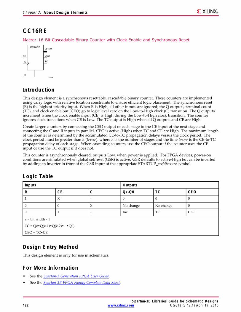
Chapter 2: About Design Elements
CC16REMacro: 16-Bit Cascadable Binary Counter with Clock Enable and Synchronous Reset
IntroductionThis design element is a synchronous resettable, cascadable binary counter. These counters are implementedusing carry logic with relative location constraints to ensure efficient logic placement. The synchronous reset(R) is the highest priority input. When R is High, all other inputs are ignored; the Q outputs, terminal count(TC), and clock enable out (CEO) go to logic level zero on the Low-to-High clock (C) transition. The Q outputsincrement when the clock enable input (CE) is High during the Low-to-High clock transition. The counterignores clock transitions when CE is Low. The TC output is High when all Q outputs and CE are High.
Create larger counters by connecting the CEO output of each stage to the CE input of the next stage andconnecting the C and R inputs in parallel. CEO is active (High) when TC and CE are High. The maximum lengthof the counter is determined by the accumulated CE-to-TC propagation delays versus the clock period. Theclock period must be greater than n (tCE-TC), where n is the number of stages and the time tCE-TC is the CE-to-TCpropagation delay of each stage. When cascading counters, use the CEO output if the counter uses the CEinput or use the TC output if it does not.
This counter is asynchronously cleared, outputs Low, when power is applied. .For FPGA devices, power-onconditions are simulated when global set/reset (GSR) is active. GSR defaults to active-High but can be invertedby adding an inverter in front of the GSR input of the appropriate STARTUP_architecture symbol.
Logic TableInputs Outputs
R CE C Qz-Q0 TC CEO1 X ↑ 0 0 0
0 0 X No change No change 0
0 1 ↑ Inc TC CEO
z = bit width - 1
TC = Qz•Q(z-1)•Q(z-2)•...•Q0)
CEO = TC•CE
Design Entry MethodThis design element is only for use in schematics.
For More Information• See the Spartan-3 Generation FPGA User Guide.• See the Spartan-3E FPGA Family Complete Data Sheet.
Spartan-3E Libraries Guide for Schematic Designs122 www.xilinx.com UG618 (v 12.1) April 19, 2010
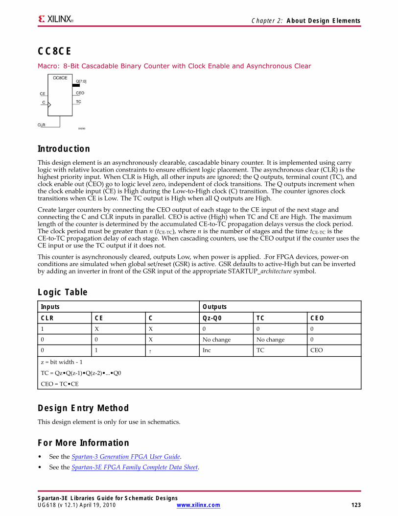
Chapter 2: About Design Elements
CC8CEMacro: 8-Bit Cascadable Binary Counter with Clock Enable and Asynchronous Clear
IntroductionThis design element is an asynchronously clearable, cascadable binary counter. It is implemented using carrylogic with relative location constraints to ensure efficient logic placement. The asynchronous clear (CLR) is thehighest priority input. When CLR is High, all other inputs are ignored; the Q outputs, terminal count (TC), andclock enable out (CEO) go to logic level zero, independent of clock transitions. The Q outputs increment whenthe clock enable input (CE) is High during the Low-to-High clock (C) transition. The counter ignores clocktransitions when CE is Low. The TC output is High when all Q outputs are High.
Create larger counters by connecting the CEO output of each stage to the CE input of the next stage andconnecting the C and CLR inputs in parallel. CEO is active (High) when TC and CE are High. The maximumlength of the counter is determined by the accumulated CE-to-TC propagation delays versus the clock period.The clock period must be greater than n (tCE-TC), where n is the number of stages and the time tCE-TC is theCE-to-TC propagation delay of each stage. When cascading counters, use the CEO output if the counter uses theCE input or use the TC output if it does not.
This counter is asynchronously cleared, outputs Low, when power is applied. .For FPGA devices, power-onconditions are simulated when global set/reset (GSR) is active. GSR defaults to active-High but can be invertedby adding an inverter in front of the GSR input of the appropriate STARTUP_architecture symbol.
Logic TableInputs Outputs
CLR CE C Qz-Q0 TC CEO1 X X 0 0 0
0 0 X No change No change 0
0 1 ↑ Inc TC CEO
z = bit width - 1
TC = Qz•Q(z-1)•Q(z-2)•...•Q0
CEO = TC•CE
Design Entry MethodThis design element is only for use in schematics.
For More Information• See the Spartan-3 Generation FPGA User Guide.• See the Spartan-3E FPGA Family Complete Data Sheet.
Spartan-3E Libraries Guide for Schematic DesignsUG618 (v 12.1) April 19, 2010 www.xilinx.com 123
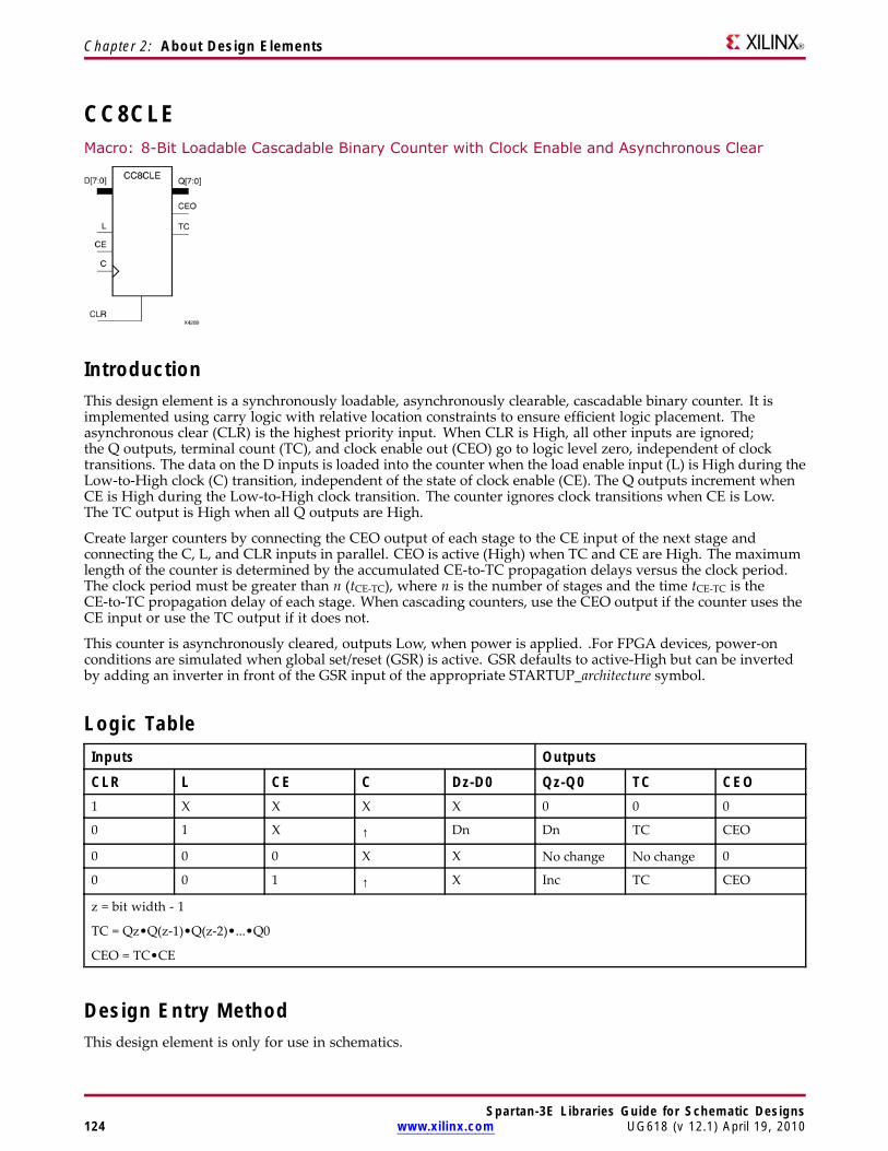
Chapter 2: About Design Elements
CC8CLEMacro: 8-Bit Loadable Cascadable Binary Counter with Clock Enable and Asynchronous Clear
IntroductionThis design element is a synchronously loadable, asynchronously clearable, cascadable binary counter. It isimplemented using carry logic with relative location constraints to ensure efficient logic placement. Theasynchronous clear (CLR) is the highest priority input. When CLR is High, all other inputs are ignored;the Q outputs, terminal count (TC), and clock enable out (CEO) go to logic level zero, independent of clocktransitions. The data on the D inputs is loaded into the counter when the load enable input (L) is High during theLow-to-High clock (C) transition, independent of the state of clock enable (CE). The Q outputs increment whenCE is High during the Low-to-High clock transition. The counter ignores clock transitions when CE is Low.The TC output is High when all Q outputs are High.
Create larger counters by connecting the CEO output of each stage to the CE input of the next stage andconnecting the C, L, and CLR inputs in parallel. CEO is active (High) when TC and CE are High. The maximumlength of the counter is determined by the accumulated CE-to-TC propagation delays versus the clock period.The clock period must be greater than n (tCE-TC), where n is the number of stages and the time tCE-TC is theCE-to-TC propagation delay of each stage. When cascading counters, use the CEO output if the counter uses theCE input or use the TC output if it does not.
This counter is asynchronously cleared, outputs Low, when power is applied. .For FPGA devices, power-onconditions are simulated when global set/reset (GSR) is active. GSR defaults to active-High but can be invertedby adding an inverter in front of the GSR input of the appropriate STARTUP_architecture symbol.
Logic TableInputs Outputs
CLR L CE C Dz-D0 Qz-Q0 TC CEO1 X X X X 0 0 0
0 1 X ↑ Dn Dn TC CEO
0 0 0 X X No change No change 0
0 0 1 ↑ X Inc TC CEO
z = bit width - 1
TC = Qz•Q(z-1)•Q(z-2)•...•Q0
CEO = TC•CE
Design Entry MethodThis design element is only for use in schematics.
Spartan-3E Libraries Guide for Schematic Designs124 www.xilinx.com UG618 (v 12.1) April 19, 2010

Chapter 2: About Design Elements
For More Information• See the Spartan-3 Generation FPGA User Guide.
• See the Spartan-3E FPGA Family Complete Data Sheet.
Spartan-3E Libraries Guide for Schematic DesignsUG618 (v 12.1) April 19, 2010 www.xilinx.com 125
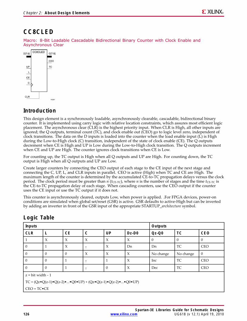
Chapter 2: About Design Elements
CC8CLEDMacro: 8-Bit Loadable Cascadable Bidirectional Binary Counter with Clock Enable andAsynchronous Clear
IntroductionThis design element is a synchronously loadable, asynchronously clearable, cascadable, bidirectional binarycounter. It is implemented using carry logic with relative location constraints, which assures most efficient logicplacement. The asynchronous clear (CLR) is the highest priority input. When CLR is High, all other inputs areignored; the Q outputs, terminal count (TC), and clock enable out (CEO) go to logic level zero, independent ofclock transitions. The data on the D inputs is loaded into the counter when the load enable input (L) is Highduring the Low-to-High clock (C) transition, independent of the state of clock enable (CE). The Q outputsdecrement when CE is High and UP is Low during the Low-to-High clock transition. The Q outputs incrementwhen CE and UP are High. The counter ignores clock transitions when CE is Low.
For counting up, the TC output is High when all Q outputs and UP are High. For counting down, the TCoutput is High when all Q outputs and UP are Low.
Create larger counters by connecting the CEO output of each stage to the CE input of the next stage andconnecting the C, UP, L, and CLR inputs in parallel. CEO is active (High) when TC and CE are High. Themaximum length of the counter is determined by the accumulated CE-to-TC propagation delays versus the clockperiod. The clock period must be greater than n (tCE-TC), where n is the number of stages and the time tCE-TC isthe CE-to-TC propagation delay of each stage. When cascading counters, use the CEO output if the counteruses the CE input or use the TC output if it does not.
This counter is asynchronously cleared, outputs Low, when power is applied. .For FPGA devices, power-onconditions are simulated when global set/reset (GSR) is active. GSR defaults to active-High but can be invertedby adding an inverter in front of the GSR input of the appropriate STARTUP_architecture symbol.
Logic TableInputs Outputs
CLR L CE C UP Dz-D0 Qz-Q0 TC CEO1 X X X X X 0 0 0
0 1 X ↑ X Dn Dn TC CEO
0 0 0 X X X No change No change 0
0 0 1 ↑ 1 X Inc TC CEO
0 0 1 ↑ 0 X Dec TC CEO
z = bit width - 1
TC = (Qz•Q(z-1)•Q(z-2)•...•Q0•UP) + (Qz•Q(z-1)•Q(z-2)•...•Q0•UP)
CEO = TC•CE
Spartan-3E Libraries Guide for Schematic Designs126 www.xilinx.com UG618 (v 12.1) April 19, 2010

Chapter 2: About Design Elements
Design Entry MethodThis design element is only for use in schematics.
For More Information• See the Spartan-3 Generation FPGA User Guide.
• See the Spartan-3E FPGA Family Complete Data Sheet.
Spartan-3E Libraries Guide for Schematic DesignsUG618 (v 12.1) April 19, 2010 www.xilinx.com 127
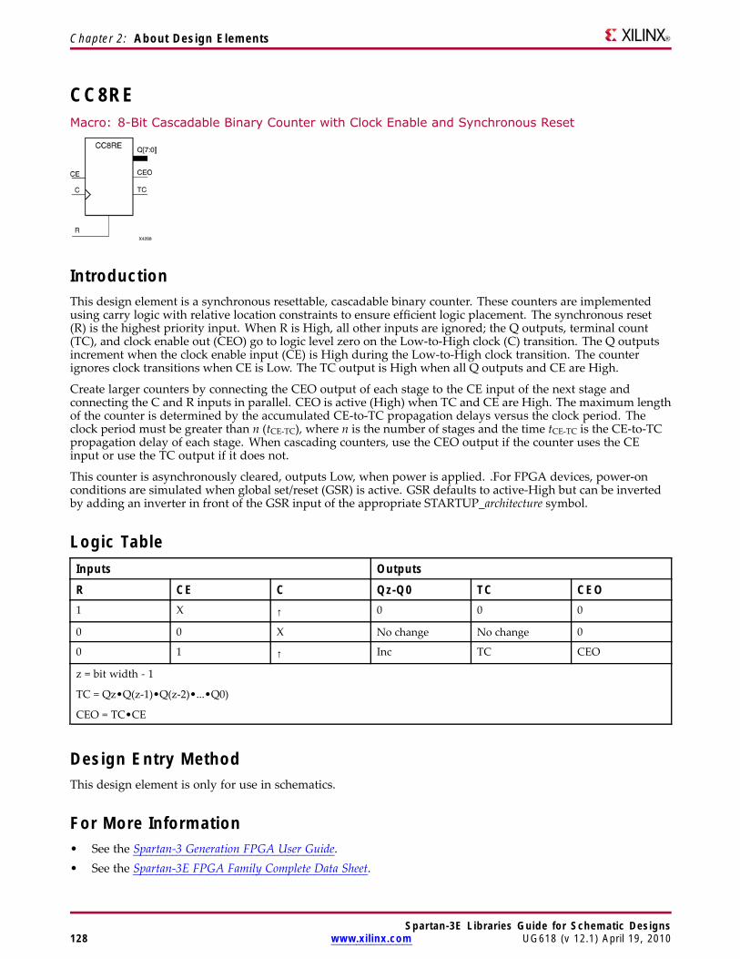
Chapter 2: About Design Elements
CC8REMacro: 8-Bit Cascadable Binary Counter with Clock Enable and Synchronous Reset
IntroductionThis design element is a synchronous resettable, cascadable binary counter. These counters are implementedusing carry logic with relative location constraints to ensure efficient logic placement. The synchronous reset(R) is the highest priority input. When R is High, all other inputs are ignored; the Q outputs, terminal count(TC), and clock enable out (CEO) go to logic level zero on the Low-to-High clock (C) transition. The Q outputsincrement when the clock enable input (CE) is High during the Low-to-High clock transition. The counterignores clock transitions when CE is Low. The TC output is High when all Q outputs and CE are High.
Create larger counters by connecting the CEO output of each stage to the CE input of the next stage andconnecting the C and R inputs in parallel. CEO is active (High) when TC and CE are High. The maximum lengthof the counter is determined by the accumulated CE-to-TC propagation delays versus the clock period. Theclock period must be greater than n (tCE-TC), where n is the number of stages and the time tCE-TC is the CE-to-TCpropagation delay of each stage. When cascading counters, use the CEO output if the counter uses the CEinput or use the TC output if it does not.
This counter is asynchronously cleared, outputs Low, when power is applied. .For FPGA devices, power-onconditions are simulated when global set/reset (GSR) is active. GSR defaults to active-High but can be invertedby adding an inverter in front of the GSR input of the appropriate STARTUP_architecture symbol.
Logic TableInputs Outputs
R CE C Qz-Q0 TC CEO1 X ↑ 0 0 0
0 0 X No change No change 0
0 1 ↑ Inc TC CEO
z = bit width - 1
TC = Qz•Q(z-1)•Q(z-2)•...•Q0)
CEO = TC•CE
Design Entry MethodThis design element is only for use in schematics.
For More Information• See the Spartan-3 Generation FPGA User Guide.• See the Spartan-3E FPGA Family Complete Data Sheet.
Spartan-3E Libraries Guide for Schematic Designs128 www.xilinx.com UG618 (v 12.1) April 19, 2010
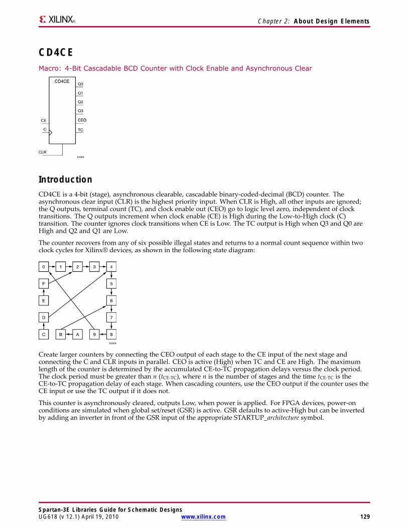
Chapter 2: About Design Elements
CD4CEMacro: 4-Bit Cascadable BCD Counter with Clock Enable and Asynchronous Clear
IntroductionCD4CE is a 4-bit (stage), asynchronous clearable, cascadable binary-coded-decimal (BCD) counter. Theasynchronous clear input (CLR) is the highest priority input. When CLR is High, all other inputs are ignored;the Q outputs, terminal count (TC), and clock enable out (CEO) go to logic level zero, independent of clocktransitions. The Q outputs increment when clock enable (CE) is High during the Low-to-High clock (C)transition. The counter ignores clock transitions when CE is Low. The TC output is High when Q3 and Q0 areHigh and Q2 and Q1 are Low.
The counter recovers from any of six possible illegal states and returns to a normal count sequence within twoclock cycles for Xilinx® devices, as shown in the following state diagram:
Create larger counters by connecting the CEO output of each stage to the CE input of the next stage andconnecting the C and CLR inputs in parallel. CEO is active (High) when TC and CE are High. The maximumlength of the counter is determined by the accumulated CE-to-TC propagation delays versus the clock period.The clock period must be greater than n (tCE-TC), where n is the number of stages and the time tCE-TC is theCE-to-TC propagation delay of each stage. When cascading counters, use the CEO output if the counter uses theCE input or use the TC output if it does not.
This counter is asynchronously cleared, outputs Low, when power is applied. For FPGA devices, power-onconditions are simulated when global set/reset (GSR) is active. GSR defaults to active-High but can be invertedby adding an inverter in front of the GSR input of the appropriate STARTUP_architecture symbol.
Spartan-3E Libraries Guide for Schematic DesignsUG618 (v 12.1) April 19, 2010 www.xilinx.com 129

Chapter 2: About Design Elements
Logic TableInputs Outputs
CLR CE C Q3 Q2 Q1 Q0 TC CEO1 X X 0 0 0 0 0 0
0 1 ↑ Inc Inc Inc Inc TC CEO
0 0 X No Change No Change No Change No Change TC 0
0 1 X 1 0 0 1 1 1
TC = Q3•!Q2•!Q1•Q0
CEO = TC•CE
Design Entry MethodThis design element is only for use in schematics.
For More Information• See the Spartan-3 Generation FPGA User Guide.
• See the Spartan-3E FPGA Family Complete Data Sheet.
Spartan-3E Libraries Guide for Schematic Designs130 www.xilinx.com UG618 (v 12.1) April 19, 2010
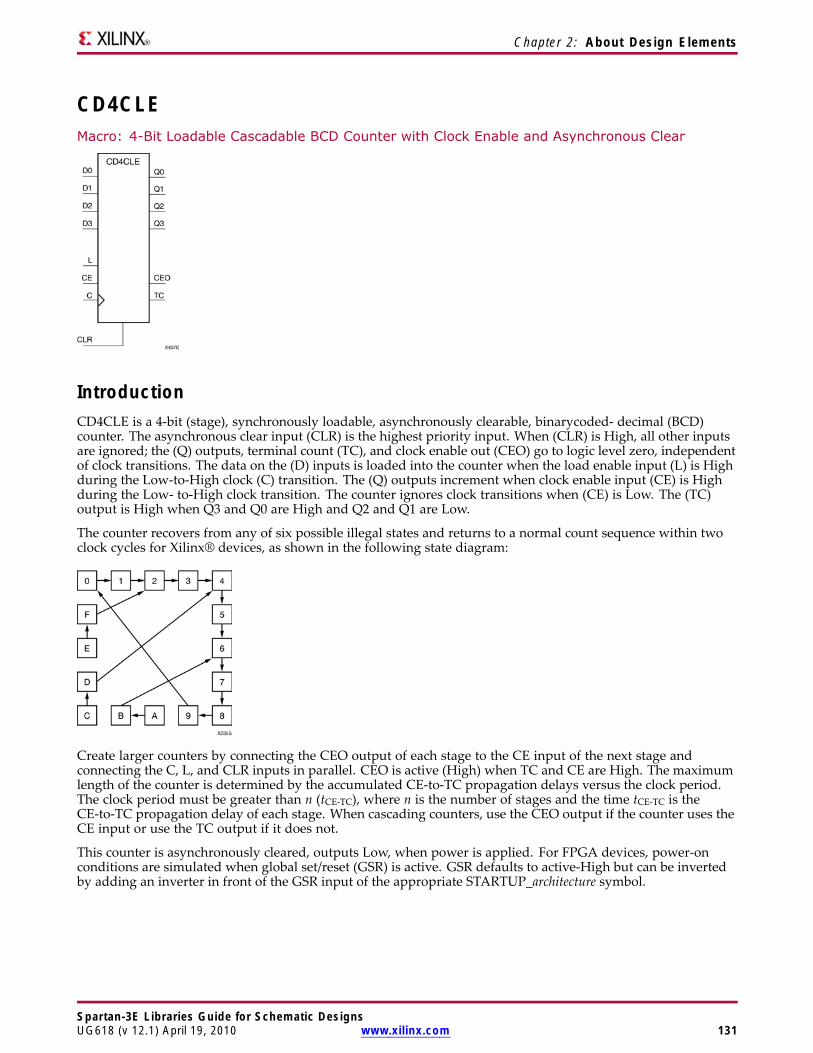
Chapter 2: About Design Elements
CD4CLEMacro: 4-Bit Loadable Cascadable BCD Counter with Clock Enable and Asynchronous Clear
IntroductionCD4CLE is a 4-bit (stage), synchronously loadable, asynchronously clearable, binarycoded- decimal (BCD)counter. The asynchronous clear input (CLR) is the highest priority input. When (CLR) is High, all other inputsare ignored; the (Q) outputs, terminal count (TC), and clock enable out (CEO) go to logic level zero, independentof clock transitions. The data on the (D) inputs is loaded into the counter when the load enable input (L) is Highduring the Low-to-High clock (C) transition. The (Q) outputs increment when clock enable input (CE) is Highduring the Low- to-High clock transition. The counter ignores clock transitions when (CE) is Low. The (TC)output is High when Q3 and Q0 are High and Q2 and Q1 are Low.
The counter recovers from any of six possible illegal states and returns to a normal count sequence within twoclock cycles for Xilinx® devices, as shown in the following state diagram:
Create larger counters by connecting the CEO output of each stage to the CE input of the next stage andconnecting the C, L, and CLR inputs in parallel. CEO is active (High) when TC and CE are High. The maximumlength of the counter is determined by the accumulated CE-to-TC propagation delays versus the clock period.The clock period must be greater than n (tCE-TC), where n is the number of stages and the time tCE-TC is theCE-to-TC propagation delay of each stage. When cascading counters, use the CEO output if the counter uses theCE input or use the TC output if it does not.
This counter is asynchronously cleared, outputs Low, when power is applied. For FPGA devices, power-onconditions are simulated when global set/reset (GSR) is active. GSR defaults to active-High but can be invertedby adding an inverter in front of the GSR input of the appropriate STARTUP_architecture symbol.
Spartan-3E Libraries Guide for Schematic DesignsUG618 (v 12.1) April 19, 2010 www.xilinx.com 131
Chapter 2: About Design Elements
Logic TableInputs Outputs
CLR L CE D3 : D0 C Q3 Q2 Q1 Q0 TC CEO1 X X X X 0 0 0 0 0 0
0 1 X D3 : D0 ↑ D3 D2 D1 D0 TC CEO
0 0 1 X ↑ Inc Inc Inc Inc TC CEO
0 0 0 X X NoChange
NoChange
NoChange
NoChange
TC 0
0 0 1 X X 1 0 0 1 1 1
TC = Q3•!Q2•!Q1•Q0
CEO = TC•CE
Design Entry MethodThis design element is only for use in schematics.
For More Information• See the Spartan-3 Generation FPGA User Guide.
• See the Spartan-3E FPGA Family Complete Data Sheet.
Spartan-3E Libraries Guide for Schematic Designs132 www.xilinx.com UG618 (v 12.1) April 19, 2010
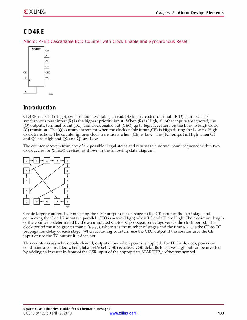
Chapter 2: About Design Elements
CD4REMacro: 4-Bit Cascadable BCD Counter with Clock Enable and Synchronous Reset
IntroductionCD4RE is a 4-bit (stage), synchronous resettable, cascadable binary-coded-decimal (BCD) counter. Thesynchronous reset input (R) is the highest priority input. When (R) is High, all other inputs are ignored; the(Q) outputs, terminal count (TC), and clock enable out (CEO) go to logic level zero on the Low-to-High clock(C) transition. The (Q) outputs increment when the clock enable input (CE) is High during the Low-to- Highclock transition. The counter ignores clock transitions when (CE) is Low. The (TC) output is High when Q3and Q0 are High and Q2 and Q1 are Low.
The counter recovers from any of six possible illegal states and returns to a normal count sequence within twoclock cycles for Xilinx® devices, as shown in the following state diagram:
Create larger counters by connecting the CEO output of each stage to the CE input of the next stage andconnecting the C and R inputs in parallel. CEO is active (High) when TC and CE are High. The maximum lengthof the counter is determined by the accumulated CE-to-TC propagation delays versus the clock period. Theclock period must be greater than n (tCE-TC), where n is the number of stages and the time tCE-TC is the CE-to-TCpropagation delay of each stage. When cascading counters, use the CEO output if the counter uses the CEinput or use the TC output if it does not.
This counter is asynchronously cleared, outputs Low, when power is applied. For FPGA devices, power-onconditions are simulated when global set/reset (GSR) is active. GSR defaults to active-High but can be invertedby adding an inverter in front of the GSR input of the appropriate STARTUP_architecture symbol.
Spartan-3E Libraries Guide for Schematic DesignsUG618 (v 12.1) April 19, 2010 www.xilinx.com 133
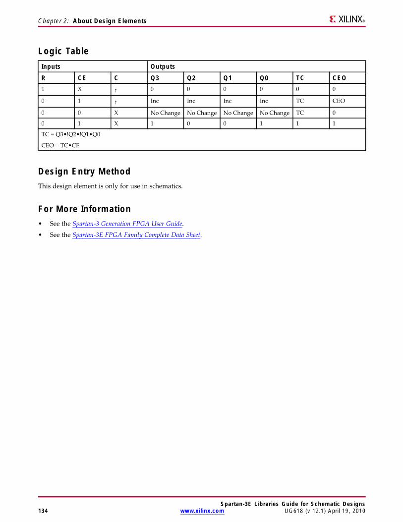
Chapter 2: About Design Elements
Logic TableInputs Outputs
R CE C Q3 Q2 Q1 Q0 TC CEO1 X ↑ 0 0 0 0 0 0
0 1 ↑ Inc Inc Inc Inc TC CEO
0 0 X No Change No Change No Change No Change TC 0
0 1 X 1 0 0 1 1 1
TC = Q3•!Q2•!Q1•Q0
CEO = TC•CE
Design Entry MethodThis design element is only for use in schematics.
For More Information• See the Spartan-3 Generation FPGA User Guide.
• See the Spartan-3E FPGA Family Complete Data Sheet.
Spartan-3E Libraries Guide for Schematic Designs134 www.xilinx.com UG618 (v 12.1) April 19, 2010
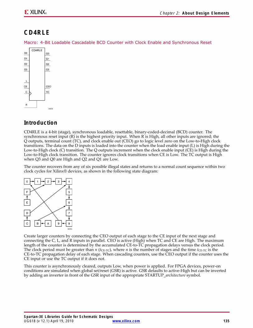
Chapter 2: About Design Elements
CD4RLEMacro: 4-Bit Loadable Cascadable BCD Counter with Clock Enable and Synchronous Reset
IntroductionCD4RLE is a 4-bit (stage), synchronous loadable, resettable, binary-coded-decimal (BCD) counter. Thesynchronous reset input (R) is the highest priority input. When R is High, all other inputs are ignored; theQ outputs, terminal count (TC), and clock enable out (CEO) go to logic level zero on the Low-to-High clocktransitions. The data on the D inputs is loaded into the counter when the load enable input (L) is High during theLow-to-High clock (C) transition. The Q outputs increment when the clock enable input (CE) is High during theLow-to-High clock transition. The counter ignores clock transitions when CE is Low. The TC output is Highwhen Q3 and Q0 are High and Q2 and Q1 are Low.
The counter recovers from any of six possible illegal states and returns to a normal count sequence within twoclock cycles for Xilinx® devices, as shown in the following state diagram:
Create larger counters by connecting the CEO output of each stage to the CE input of the next stage andconnecting the C, L, and R inputs in parallel. CEO is active (High) when TC and CE are High. The maximumlength of the counter is determined by the accumulated CE-to-TC propagation delays versus the clock period.The clock period must be greater than n (tCE-TC), where n is the number of stages and the time tCE-TC is theCE-to-TC propagation delay of each stage. When cascading counters, use the CEO output if the counter uses theCE input or use the TC output if it does not.
This counter is asynchronously cleared, outputs Low, when power is applied. For FPGA devices, power-onconditions are simulated when global set/reset (GSR) is active. GSR defaults to active-High but can be invertedby adding an inverter in front of the GSR input of the appropriate STARTUP_architecture symbol.
Spartan-3E Libraries Guide for Schematic DesignsUG618 (v 12.1) April 19, 2010 www.xilinx.com 135
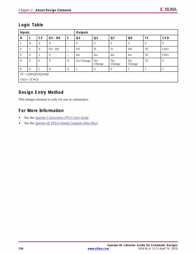
Chapter 2: About Design Elements
Logic TableInputs Outputs
R L CE D3 : D0 C Q3 Q2 Q1 Q0 TC CEO1 X X X ↑ 0 0 0 0 0 0
0 1 X D3 : D0 ↑ D3 D D D0 TC CEO
0 0 1 X ↑ Inc Inc Inc Inc TC CEO
0 0 0 X X No Change NoChange
NoChange
NoChange
TC 0
0 0 1 X X 1 0 0 1 1 1
TC = Q3•!Q2•!Q1•Q0
CEO = TC•CE
Design Entry MethodThis design element is only for use in schematics.
For More Information• See the Spartan-3 Generation FPGA User Guide.
• See the Spartan-3E FPGA Family Complete Data Sheet.
Spartan-3E Libraries Guide for Schematic Designs136 www.xilinx.com UG618 (v 12.1) April 19, 2010
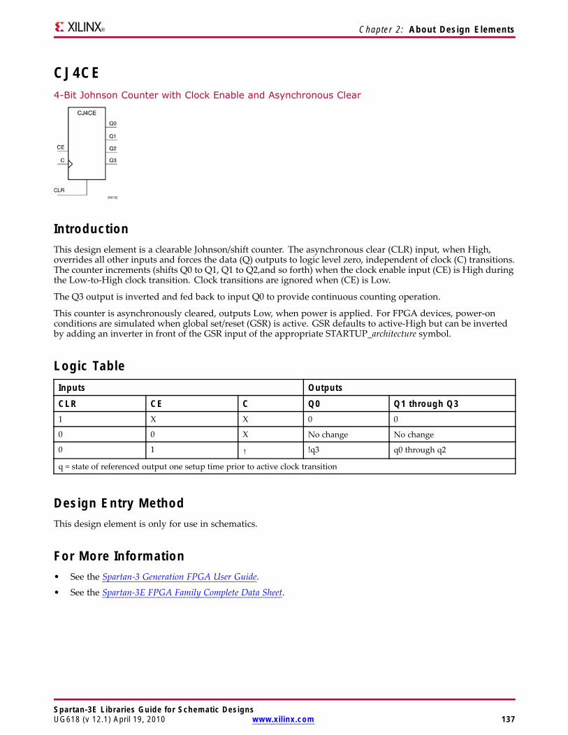
Chapter 2: About Design Elements
CJ4CE4-Bit Johnson Counter with Clock Enable and Asynchronous Clear
IntroductionThis design element is a clearable Johnson/shift counter. The asynchronous clear (CLR) input, when High,overrides all other inputs and forces the data (Q) outputs to logic level zero, independent of clock (C) transitions.The counter increments (shifts Q0 to Q1, Q1 to Q2,and so forth) when the clock enable input (CE) is High duringthe Low-to-High clock transition. Clock transitions are ignored when (CE) is Low.
The Q3 output is inverted and fed back to input Q0 to provide continuous counting operation.
This counter is asynchronously cleared, outputs Low, when power is applied. For FPGA devices, power-onconditions are simulated when global set/reset (GSR) is active. GSR defaults to active-High but can be invertedby adding an inverter in front of the GSR input of the appropriate STARTUP_architecture symbol.
Logic TableInputs Outputs
CLR CE C Q0 Q1 through Q31 X X 0 0
0 0 X No change No change
0 1 ↑ !q3 q0 through q2
q = state of referenced output one setup time prior to active clock transition
Design Entry MethodThis design element is only for use in schematics.
For More Information• See the Spartan-3 Generation FPGA User Guide.
• See the Spartan-3E FPGA Family Complete Data Sheet.
Spartan-3E Libraries Guide for Schematic DesignsUG618 (v 12.1) April 19, 2010 www.xilinx.com 137
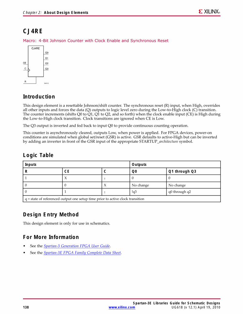
Chapter 2: About Design Elements
CJ4REMacro: 4-Bit Johnson Counter with Clock Enable and Synchronous Reset
IntroductionThis design element is a resettable Johnson/shift counter. The synchronous reset (R) input, when High, overridesall other inputs and forces the data (Q) outputs to logic level zero during the Low-to-High clock (C) transition.The counter increments (shifts Q0 to Q1, Q1 to Q2, and so forth) when the clock enable input (CE) is High duringthe Low-to-High clock transition. Clock transitions are ignored when CE is Low.
The Q3 output is inverted and fed back to input Q0 to provide continuous counting operation.
This counter is asynchronously cleared, outputs Low, when power is applied. For FPGA devices, power-onconditions are simulated when global set/reset (GSR) is active. GSR defaults to active-High but can be invertedby adding an inverter in front of the GSR input of the appropriate STARTUP_architecture symbol.
Logic TableInputs Outputs
R CE C Q0 Q1 through Q31 X ↑ 0 0
0 0 X No change No change
0 1 ↑ !q3 q0 through q2
q = state of referenced output one setup time prior to active clock transition
Design Entry MethodThis design element is only for use in schematics.
For More Information• See the Spartan-3 Generation FPGA User Guide.
• See the Spartan-3E FPGA Family Complete Data Sheet.
Spartan-3E Libraries Guide for Schematic Designs138 www.xilinx.com UG618 (v 12.1) April 19, 2010
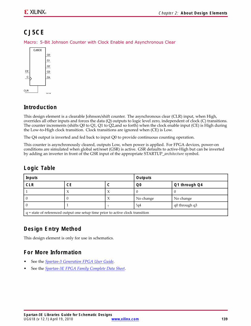
Chapter 2: About Design Elements
CJ5CEMacro: 5-Bit Johnson Counter with Clock Enable and Asynchronous Clear
IntroductionThis design element is a clearable Johnson/shift counter. The asynchronous clear (CLR) input, when High,overrides all other inputs and forces the data (Q) outputs to logic level zero, independent of clock (C) transitions.The counter increments (shifts Q0 to Q1, Q1 to Q2,and so forth) when the clock enable input (CE) is High duringthe Low-to-High clock transition. Clock transitions are ignored when (CE) is Low.
The Q4 output is inverted and fed back to input Q0 to provide continuous counting operation.
This counter is asynchronously cleared, outputs Low, when power is applied. For FPGA devices, power-onconditions are simulated when global set/reset (GSR) is active. GSR defaults to active-High but can be invertedby adding an inverter in front of the GSR input of the appropriate STARTUP_architecture symbol.
Logic TableInputs Outputs
CLR CE C Q0 Q1 through Q41 X X 0 0
0 0 X No change No change
0 1 ↑ !q4 q0 through q3
q = state of referenced output one setup time prior to active clock transition
Design Entry MethodThis design element is only for use in schematics.
For More Information• See the Spartan-3 Generation FPGA User Guide.
• See the Spartan-3E FPGA Family Complete Data Sheet.
Spartan-3E Libraries Guide for Schematic DesignsUG618 (v 12.1) April 19, 2010 www.xilinx.com 139
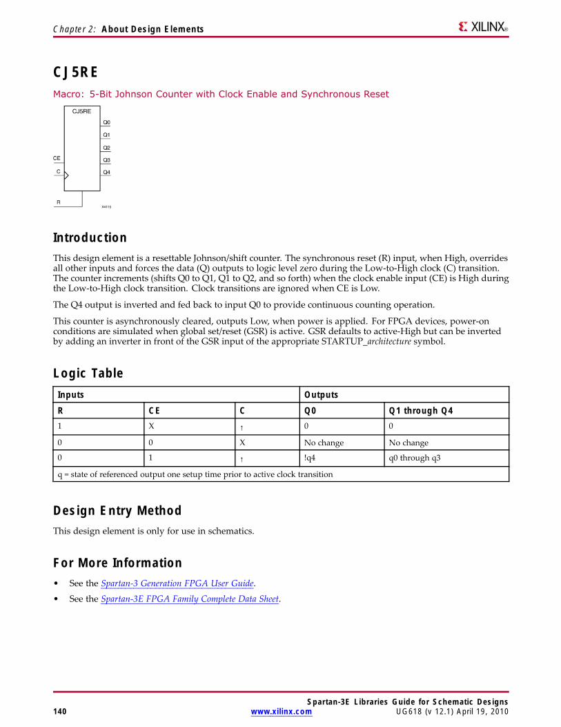
Chapter 2: About Design Elements
CJ5REMacro: 5-Bit Johnson Counter with Clock Enable and Synchronous Reset
IntroductionThis design element is a resettable Johnson/shift counter. The synchronous reset (R) input, when High, overridesall other inputs and forces the data (Q) outputs to logic level zero during the Low-to-High clock (C) transition.The counter increments (shifts Q0 to Q1, Q1 to Q2, and so forth) when the clock enable input (CE) is High duringthe Low-to-High clock transition. Clock transitions are ignored when CE is Low.
The Q4 output is inverted and fed back to input Q0 to provide continuous counting operation.
This counter is asynchronously cleared, outputs Low, when power is applied. For FPGA devices, power-onconditions are simulated when global set/reset (GSR) is active. GSR defaults to active-High but can be invertedby adding an inverter in front of the GSR input of the appropriate STARTUP_architecture symbol.
Logic TableInputs Outputs
R CE C Q0 Q1 through Q41 X ↑ 0 0
0 0 X No change No change
0 1 ↑ !q4 q0 through q3
q = state of referenced output one setup time prior to active clock transition
Design Entry MethodThis design element is only for use in schematics.
For More Information• See the Spartan-3 Generation FPGA User Guide.
• See the Spartan-3E FPGA Family Complete Data Sheet.
Spartan-3E Libraries Guide for Schematic Designs140 www.xilinx.com UG618 (v 12.1) April 19, 2010
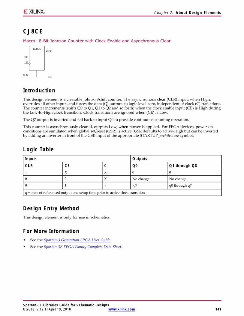
Chapter 2: About Design Elements
CJ8CEMacro: 8-Bit Johnson Counter with Clock Enable and Asynchronous Clear
IntroductionThis design element is a clearable Johnson/shift counter. The asynchronous clear (CLR) input, when High,overrides all other inputs and forces the data (Q) outputs to logic level zero, independent of clock (C) transitions.The counter increments (shifts Q0 to Q1, Q1 to Q2,and so forth) when the clock enable input (CE) is High duringthe Low-to-High clock transition. Clock transitions are ignored when (CE) is Low.
The Q7 output is inverted and fed back to input Q0 to provide continuous counting operation.
This counter is asynchronously cleared, outputs Low, when power is applied. For FPGA devices, power-onconditions are simulated when global set/reset (GSR) is active. GSR defaults to active-High but can be invertedby adding an inverter in front of the GSR input of the appropriate STARTUP_architecture symbol.
Logic TableInputs Outputs
CLR CE C Q0 Q1 through Q81 X X 0 0
0 0 X No change No change
0 1 ↑ !q7 q0 through q7
q = state of referenced output one setup time prior to active clock transition
Design Entry MethodThis design element is only for use in schematics.
For More Information• See the Spartan-3 Generation FPGA User Guide.
• See the Spartan-3E FPGA Family Complete Data Sheet.
Spartan-3E Libraries Guide for Schematic DesignsUG618 (v 12.1) April 19, 2010 www.xilinx.com 141
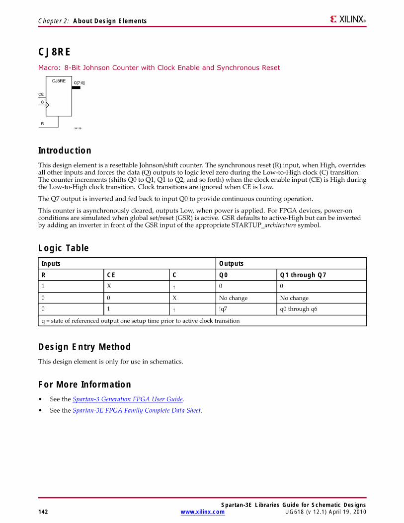
Chapter 2: About Design Elements
CJ8REMacro: 8-Bit Johnson Counter with Clock Enable and Synchronous Reset
IntroductionThis design element is a resettable Johnson/shift counter. The synchronous reset (R) input, when High, overridesall other inputs and forces the data (Q) outputs to logic level zero during the Low-to-High clock (C) transition.The counter increments (shifts Q0 to Q1, Q1 to Q2, and so forth) when the clock enable input (CE) is High duringthe Low-to-High clock transition. Clock transitions are ignored when CE is Low.
The Q7 output is inverted and fed back to input Q0 to provide continuous counting operation.
This counter is asynchronously cleared, outputs Low, when power is applied. For FPGA devices, power-onconditions are simulated when global set/reset (GSR) is active. GSR defaults to active-High but can be invertedby adding an inverter in front of the GSR input of the appropriate STARTUP_architecture symbol.
Logic TableInputs Outputs
R CE C Q0 Q1 through Q71 X ↑ 0 0
0 0 X No change No change
0 1 ↑ !q7 q0 through q6
q = state of referenced output one setup time prior to active clock transition
Design Entry MethodThis design element is only for use in schematics.
For More Information• See the Spartan-3 Generation FPGA User Guide.
• See the Spartan-3E FPGA Family Complete Data Sheet.
Spartan-3E Libraries Guide for Schematic Designs142 www.xilinx.com UG618 (v 12.1) April 19, 2010
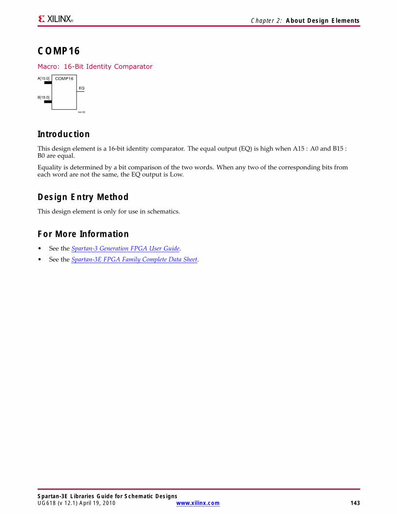
Chapter 2: About Design Elements
COMP16Macro: 16-Bit Identity Comparator
IntroductionThis design element is a 16-bit identity comparator. The equal output (EQ) is high when A15 : A0 and B15 :B0 are equal.
Equality is determined by a bit comparison of the two words. When any two of the corresponding bits fromeach word are not the same, the EQ output is Low.
Design Entry MethodThis design element is only for use in schematics.
For More Information• See the Spartan-3 Generation FPGA User Guide.
• See the Spartan-3E FPGA Family Complete Data Sheet.
Spartan-3E Libraries Guide for Schematic DesignsUG618 (v 12.1) April 19, 2010 www.xilinx.com 143
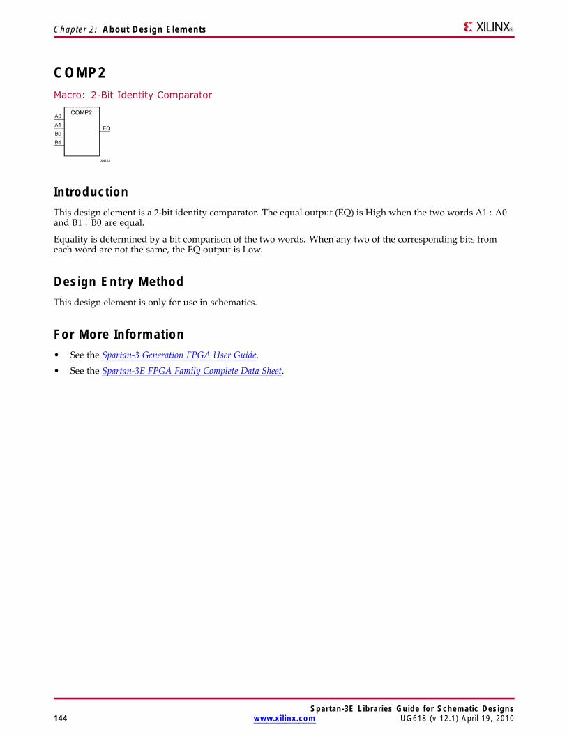
Chapter 2: About Design Elements
COMP2Macro: 2-Bit Identity Comparator
IntroductionThis design element is a 2-bit identity comparator. The equal output (EQ) is High when the two words A1 : A0and B1 : B0 are equal.
Equality is determined by a bit comparison of the two words. When any two of the corresponding bits fromeach word are not the same, the EQ output is Low.
Design Entry MethodThis design element is only for use in schematics.
For More Information• See the Spartan-3 Generation FPGA User Guide.
• See the Spartan-3E FPGA Family Complete Data Sheet.
Spartan-3E Libraries Guide for Schematic Designs144 www.xilinx.com UG618 (v 12.1) April 19, 2010
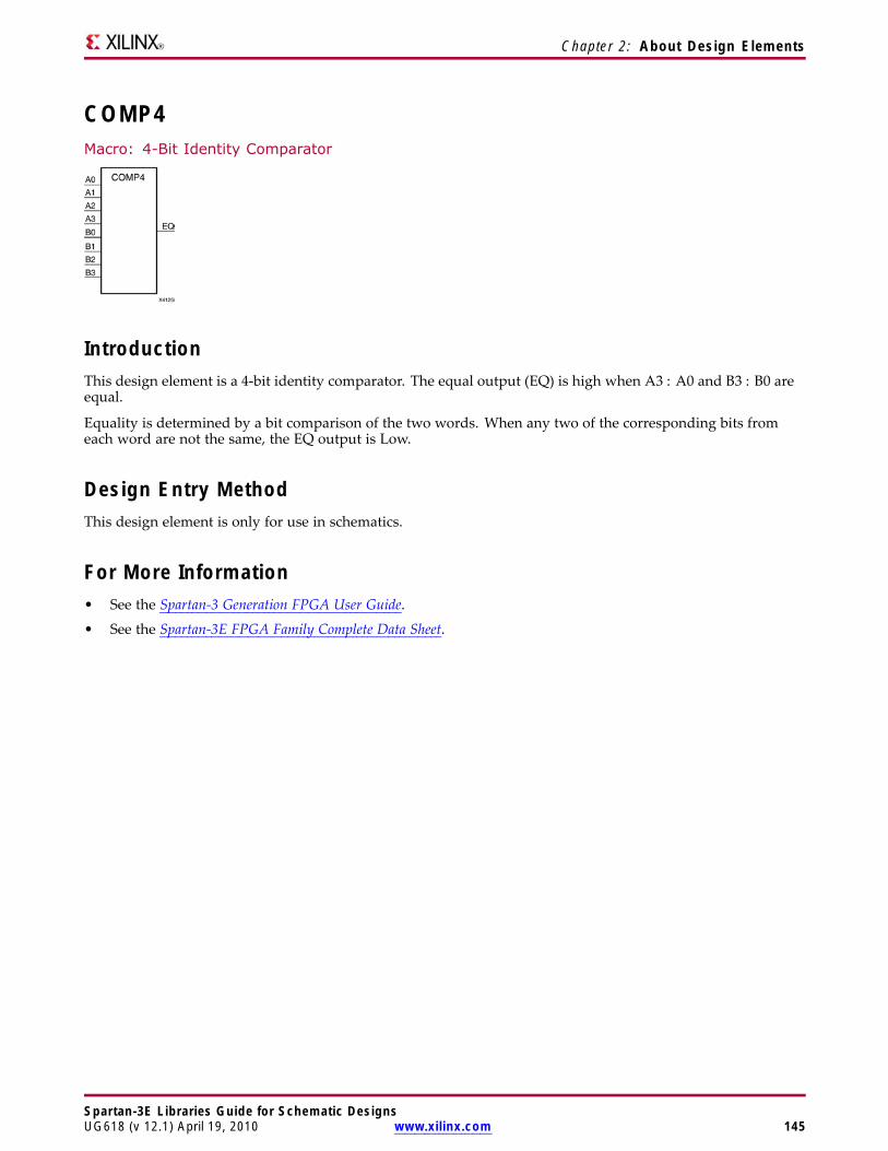
Chapter 2: About Design Elements
COMP4Macro: 4-Bit Identity Comparator
IntroductionThis design element is a 4-bit identity comparator. The equal output (EQ) is high when A3 : A0 and B3 : B0 areequal.
Equality is determined by a bit comparison of the two words. When any two of the corresponding bits fromeach word are not the same, the EQ output is Low.
Design Entry MethodThis design element is only for use in schematics.
For More Information• See the Spartan-3 Generation FPGA User Guide.
• See the Spartan-3E FPGA Family Complete Data Sheet.
Spartan-3E Libraries Guide for Schematic DesignsUG618 (v 12.1) April 19, 2010 www.xilinx.com 145
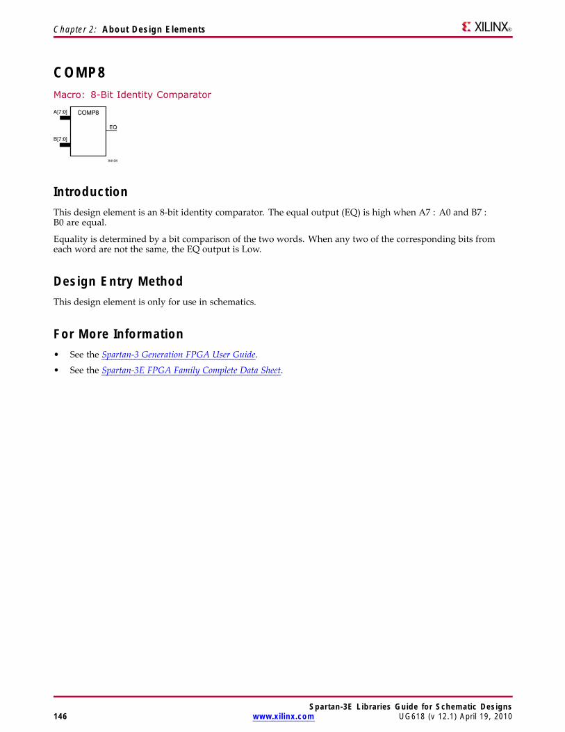
Chapter 2: About Design Elements
COMP8Macro: 8-Bit Identity Comparator
IntroductionThis design element is an 8-bit identity comparator. The equal output (EQ) is high when A7 : A0 and B7 :B0 are equal.
Equality is determined by a bit comparison of the two words. When any two of the corresponding bits fromeach word are not the same, the EQ output is Low.
Design Entry MethodThis design element is only for use in schematics.
For More Information• See the Spartan-3 Generation FPGA User Guide.
• See the Spartan-3E FPGA Family Complete Data Sheet.
Spartan-3E Libraries Guide for Schematic Designs146 www.xilinx.com UG618 (v 12.1) April 19, 2010
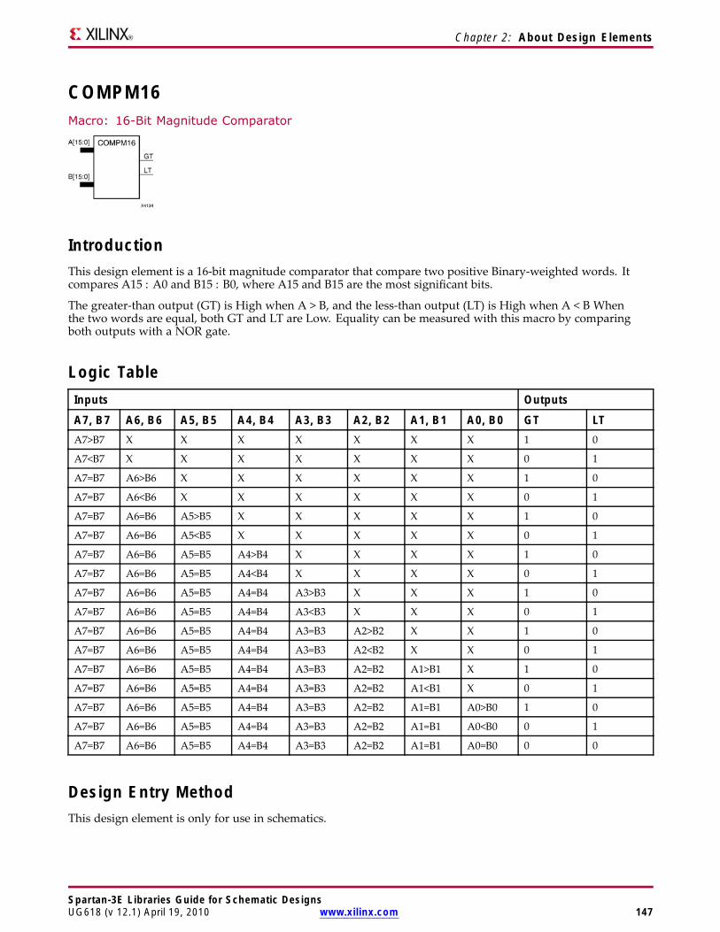
Chapter 2: About Design Elements
COMPM16Macro: 16-Bit Magnitude Comparator
IntroductionThis design element is a 16-bit magnitude comparator that compare two positive Binary-weighted words. Itcompares A15 : A0 and B15 : B0, where A15 and B15 are the most significant bits.
The greater-than output (GT) is High when A > B, and the less-than output (LT) is High when A < B Whenthe two words are equal, both GT and LT are Low. Equality can be measured with this macro by comparingboth outputs with a NOR gate.
Logic TableInputs Outputs
A7, B7 A6, B6 A5, B5 A4, B4 A3, B3 A2, B2 A1, B1 A0, B0 GT LTA7>B7 X X X X X X X 1 0
A7<B7 X X X X X X X 0 1
A7=B7 A6>B6 X X X X X X 1 0
A7=B7 A6<B6 X X X X X X 0 1
A7=B7 A6=B6 A5>B5 X X X X X 1 0
A7=B7 A6=B6 A5<B5 X X X X X 0 1
A7=B7 A6=B6 A5=B5 A4>B4 X X X X 1 0
A7=B7 A6=B6 A5=B5 A4<B4 X X X X 0 1
A7=B7 A6=B6 A5=B5 A4=B4 A3>B3 X X X 1 0
A7=B7 A6=B6 A5=B5 A4=B4 A3<B3 X X X 0 1
A7=B7 A6=B6 A5=B5 A4=B4 A3=B3 A2>B2 X X 1 0
A7=B7 A6=B6 A5=B5 A4=B4 A3=B3 A2<B2 X X 0 1
A7=B7 A6=B6 A5=B5 A4=B4 A3=B3 A2=B2 A1>B1 X 1 0
A7=B7 A6=B6 A5=B5 A4=B4 A3=B3 A2=B2 A1<B1 X 0 1
A7=B7 A6=B6 A5=B5 A4=B4 A3=B3 A2=B2 A1=B1 A0>B0 1 0
A7=B7 A6=B6 A5=B5 A4=B4 A3=B3 A2=B2 A1=B1 A0<B0 0 1
A7=B7 A6=B6 A5=B5 A4=B4 A3=B3 A2=B2 A1=B1 A0=B0 0 0
Design Entry MethodThis design element is only for use in schematics.
Spartan-3E Libraries Guide for Schematic DesignsUG618 (v 12.1) April 19, 2010 www.xilinx.com 147

Chapter 2: About Design Elements
For More Information• See the Spartan-3 Generation FPGA User Guide.
• See the Spartan-3E FPGA Family Complete Data Sheet.
Spartan-3E Libraries Guide for Schematic Designs148 www.xilinx.com UG618 (v 12.1) April 19, 2010
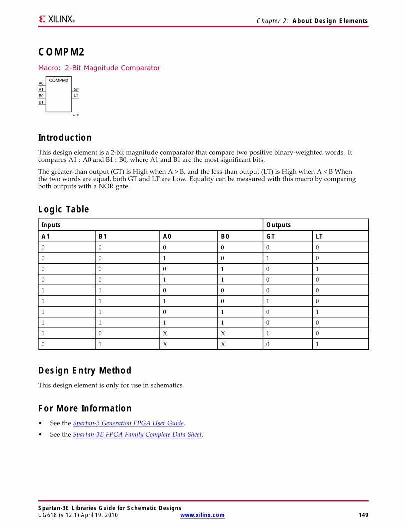
Chapter 2: About Design Elements
COMPM2Macro: 2-Bit Magnitude Comparator
IntroductionThis design element is a 2-bit magnitude comparator that compare two positive binary-weighted words. Itcompares A1 : A0 and B1 : B0, where A1 and B1 are the most significant bits.
The greater-than output (GT) is High when A > B, and the less-than output (LT) is High when A < B Whenthe two words are equal, both GT and LT are Low. Equality can be measured with this macro by comparingboth outputs with a NOR gate.
Logic TableInputs Outputs
A1 B1 A0 B0 GT LT0 0 0 0 0 0
0 0 1 0 1 0
0 0 0 1 0 1
0 0 1 1 0 0
1 1 0 0 0 0
1 1 1 0 1 0
1 1 0 1 0 1
1 1 1 1 0 0
1 0 X X 1 0
0 1 X X 0 1
Design Entry MethodThis design element is only for use in schematics.
For More Information• See the Spartan-3 Generation FPGA User Guide.
• See the Spartan-3E FPGA Family Complete Data Sheet.
Spartan-3E Libraries Guide for Schematic DesignsUG618 (v 12.1) April 19, 2010 www.xilinx.com 149
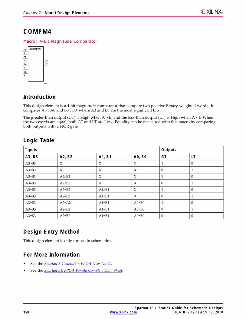
Chapter 2: About Design Elements
COMPM4Macro: 4-Bit Magnitude Comparator
IntroductionThis design element is a 4-bit magnitude comparator that compare two positive Binary-weighted words. Itcompares A3 : A0 and B3 : B0, where A3 and B3 are the most significant bits.
The greater-than output (GT) is High when A > B, and the less-than output (LT) is High when A < B Whenthe two words are equal, both GT and LT are Low. Equality can be measured with this macro by comparingboth outputs with a NOR gate.
Logic TableInputs Outputs
A3, B3 A2, B2 A1, B1 A0, B0 GT LTA3>B3 X X X 1 0
A3<B3 X X X 0 1
A3=B3 A2>B2 X X 1 0
A3=B3 A2<B2 X X 0 1
A3=B3 A2=B2 A1>B1 X 1 0
A3=B3 A2=B2 A1<B1 X 0 1
A3=B3 A2=A2 A1=B1 A0>B0 1 0
A3=B3 A2=B2 A1=B1 A0<B0 0 1
A3=B3 A2=B2 A1=B1 A0=B0 0 0
Design Entry MethodThis design element is only for use in schematics.
For More Information• See the Spartan-3 Generation FPGA User Guide.
• See the Spartan-3E FPGA Family Complete Data Sheet.
Spartan-3E Libraries Guide for Schematic Designs150 www.xilinx.com UG618 (v 12.1) April 19, 2010
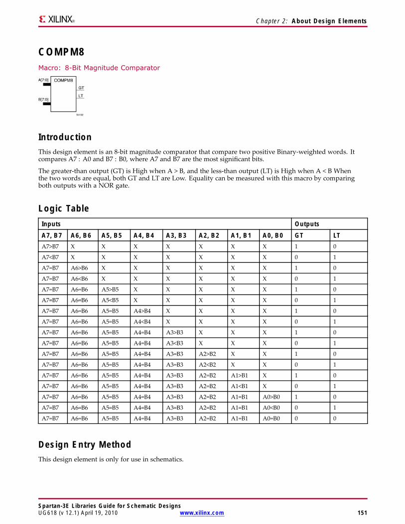
Chapter 2: About Design Elements
COMPM8Macro: 8-Bit Magnitude Comparator
IntroductionThis design element is an 8-bit magnitude comparator that compare two positive Binary-weighted words. Itcompares A7 : A0 and B7 : B0, where A7 and B7 are the most significant bits.
The greater-than output (GT) is High when A > B, and the less-than output (LT) is High when A < B Whenthe two words are equal, both GT and LT are Low. Equality can be measured with this macro by comparingboth outputs with a NOR gate.
Logic TableInputs Outputs
A7, B7 A6, B6 A5, B5 A4, B4 A3, B3 A2, B2 A1, B1 A0, B0 GT LTA7>B7 X X X X X X X 1 0
A7<B7 X X X X X X X 0 1
A7=B7 A6>B6 X X X X X X 1 0
A7=B7 A6<B6 X X X X X X 0 1
A7=B7 A6=B6 A5>B5 X X X X X 1 0
A7=B7 A6=B6 A5<B5 X X X X X 0 1
A7=B7 A6=B6 A5=B5 A4>B4 X X X X 1 0
A7=B7 A6=B6 A5=B5 A4<B4 X X X X 0 1
A7=B7 A6=B6 A5=B5 A4=B4 A3>B3 X X X 1 0
A7=B7 A6=B6 A5=B5 A4=B4 A3<B3 X X X 0 1
A7=B7 A6=B6 A5=B5 A4=B4 A3=B3 A2>B2 X X 1 0
A7=B7 A6=B6 A5=B5 A4=B4 A3=B3 A2<B2 X X 0 1
A7=B7 A6=B6 A5=B5 A4=B4 A3=B3 A2=B2 A1>B1 X 1 0
A7=B7 A6=B6 A5=B5 A4=B4 A3=B3 A2=B2 A1<B1 X 0 1
A7=B7 A6=B6 A5=B5 A4=B4 A3=B3 A2=B2 A1=B1 A0>B0 1 0
A7=B7 A6=B6 A5=B5 A4=B4 A3=B3 A2=B2 A1=B1 A0<B0 0 1
A7=B7 A6=B6 A5=B5 A4=B4 A3=B3 A2=B2 A1=B1 A0=B0 0 0
Design Entry MethodThis design element is only for use in schematics.
Spartan-3E Libraries Guide for Schematic DesignsUG618 (v 12.1) April 19, 2010 www.xilinx.com 151

Chapter 2: About Design Elements
For More Information• See the Spartan-3 Generation FPGA User Guide.
• See the Spartan-3E FPGA Family Complete Data Sheet.
Spartan-3E Libraries Guide for Schematic Designs152 www.xilinx.com UG618 (v 12.1) April 19, 2010
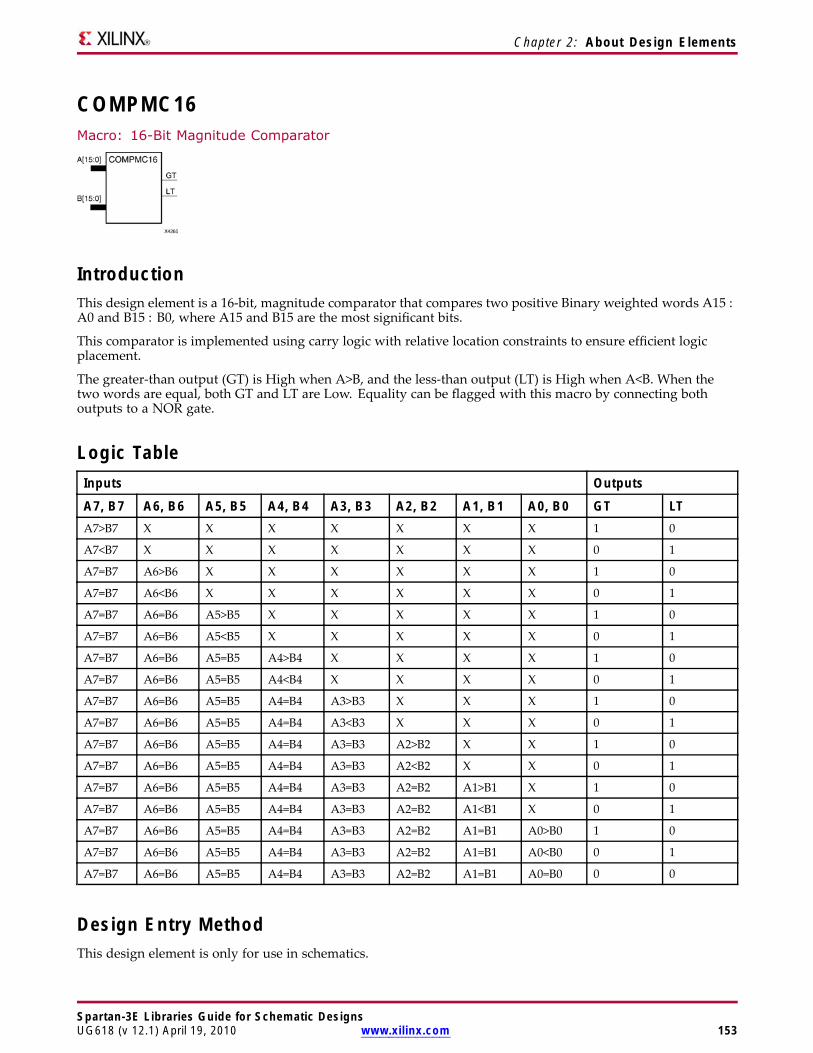
Chapter 2: About Design Elements
COMPMC16Macro: 16-Bit Magnitude Comparator
IntroductionThis design element is a 16-bit, magnitude comparator that compares two positive Binary weighted words A15 :A0 and B15 : B0, where A15 and B15 are the most significant bits.
This comparator is implemented using carry logic with relative location constraints to ensure efficient logicplacement.
The greater-than output (GT) is High when A>B, and the less-than output (LT) is High when A<B. When thetwo words are equal, both GT and LT are Low. Equality can be flagged with this macro by connecting bothoutputs to a NOR gate.
Logic TableInputs Outputs
A7, B7 A6, B6 A5, B5 A4, B4 A3, B3 A2, B2 A1, B1 A0, B0 GT LTA7>B7 X X X X X X X 1 0
A7<B7 X X X X X X X 0 1
A7=B7 A6>B6 X X X X X X 1 0
A7=B7 A6<B6 X X X X X X 0 1
A7=B7 A6=B6 A5>B5 X X X X X 1 0
A7=B7 A6=B6 A5<B5 X X X X X 0 1
A7=B7 A6=B6 A5=B5 A4>B4 X X X X 1 0
A7=B7 A6=B6 A5=B5 A4<B4 X X X X 0 1
A7=B7 A6=B6 A5=B5 A4=B4 A3>B3 X X X 1 0
A7=B7 A6=B6 A5=B5 A4=B4 A3<B3 X X X 0 1
A7=B7 A6=B6 A5=B5 A4=B4 A3=B3 A2>B2 X X 1 0
A7=B7 A6=B6 A5=B5 A4=B4 A3=B3 A2<B2 X X 0 1
A7=B7 A6=B6 A5=B5 A4=B4 A3=B3 A2=B2 A1>B1 X 1 0
A7=B7 A6=B6 A5=B5 A4=B4 A3=B3 A2=B2 A1<B1 X 0 1
A7=B7 A6=B6 A5=B5 A4=B4 A3=B3 A2=B2 A1=B1 A0>B0 1 0
A7=B7 A6=B6 A5=B5 A4=B4 A3=B3 A2=B2 A1=B1 A0<B0 0 1
A7=B7 A6=B6 A5=B5 A4=B4 A3=B3 A2=B2 A1=B1 A0=B0 0 0
Design Entry MethodThis design element is only for use in schematics.
Spartan-3E Libraries Guide for Schematic DesignsUG618 (v 12.1) April 19, 2010 www.xilinx.com 153

Chapter 2: About Design Elements
For More Information• See the Spartan-3 Generation FPGA User Guide.
• See the Spartan-3E FPGA Family Complete Data Sheet.
Spartan-3E Libraries Guide for Schematic Designs154 www.xilinx.com UG618 (v 12.1) April 19, 2010

Chapter 2: About Design Elements
COMPMC8Macro: 8-Bit Magnitude Comparator
IntroductionThis design element is an 8-bit, magnitude comparator that compares two positive Binaryweighted words A7 :A0 and B7 : B0, where A7 and B7 are the most significant bits.
This comparator is implemented using carry logic with relative location constraints to ensure efficient logicplacement.
The greater-than output (GT) is High when A>B, and the less-than output (LT) is High when A<B. When thetwo words are equal, both GT and LT are Low. Equality can be flagged with this macro by connecting bothoutputs to a NOR gate.
Logic TableInputs Outputs
A7, B7 A6, B6 A5, B5 A4, B4 A3, B3 A2, B2 A1, B1 A0, B0 GT LTA7>B7 X X X X X X X 1 0
A7<B7 X X X X X X X 0 1
A7=B7 A6>B6 X X X X X X 1 0
A7=B7 A6<B6 X X X X X X 0 1
A7=B7 A6=B6 A5>B5 X X X X X 1 0
A7=B7 A6=B6 A5<B5 X X X X X 0 1
A7=B7 A6=B6 A5=B5 A4>B4 X X X X 1 0
A7=B7 A6=B6 A5=B5 A4<B4 X X X X 0 1
A7=B7 A6=B6 A5=B5 A4=B4 A3>B3 X X X 1 0
A7=B7 A6=B6 A5=B5 A4=B4 A3<B3 X X X 0 1
A7=B7 A6=B6 A5=B5 A4=B4 A3=B3 A2>B2 X X 1 0
A7=B7 A6=B6 A5=B5 A4=B4 A3=B3 A2<B2 X X 0 1
A7=B7 A6=B6 A5=B5 A4=B4 A3=B3 A2=B2 A1>B1 X 1 0
A7=B7 A6=B6 A5=B5 A4=B4 A3=B3 A2=B2 A1<B1 X 0 1
A7=B7 A6=B6 A5=B5 A4=B4 A3=B3 A2=B2 A1=B1 A0>B0 1 0
A7=B7 A6=B6 A5=B5 A4=B4 A3=B3 A2=B2 A1=B1 A0<B0 0 1
A7=B7 A6=B6 A5=B5 A4=B4 A3=B3 A2=B2 A1=B1 A0=B0 0 0
Design Entry MethodThis design element is only for use in schematics.
Spartan-3E Libraries Guide for Schematic DesignsUG618 (v 12.1) April 19, 2010 www.xilinx.com 155

Chapter 2: About Design Elements
For More Information• See the Spartan-3 Generation FPGA User Guide.
• See the Spartan-3E FPGA Family Complete Data Sheet.
Spartan-3E Libraries Guide for Schematic Designs156 www.xilinx.com UG618 (v 12.1) April 19, 2010
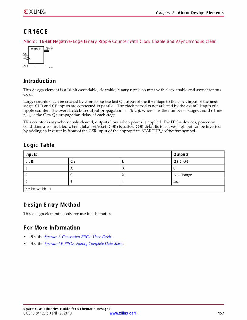
Chapter 2: About Design Elements
CR16CEMacro: 16-Bit Negative-Edge Binary Ripple Counter with Clock Enable and Asynchronous Clear
IntroductionThis design element is a 16-bit cascadable, clearable, binary ripple counter with clock enable and asynchronousclear.
Larger counters can be created by connecting the last Q output of the first stage to the clock input of the nextstage. CLR and CE inputs are connected in parallel. The clock period is not affected by the overall length of aripple counter. The overall clock-to-output propagation is n(tC - Q), where n is the number of stages and the timetC - Q is the C-to-Qz propagation delay of each stage.
This counter is asynchronously cleared, outputs Low, when power is applied. For FPGA devices, power-onconditions are simulated when global set/reset (GSR) is active. GSR defaults to active-High but can be invertedby adding an inverter in front of the GSR input of the appropriate STARTUP_architecture symbol.
Logic TableInputs Outputs
CLR CE C Qz : Q01 X X 0
0 0 X No Change
0 1 ↓ Inc
z = bit width - 1
Design Entry MethodThis design element is only for use in schematics.
For More Information• See the Spartan-3 Generation FPGA User Guide.
• See the Spartan-3E FPGA Family Complete Data Sheet.
Spartan-3E Libraries Guide for Schematic DesignsUG618 (v 12.1) April 19, 2010 www.xilinx.com 157
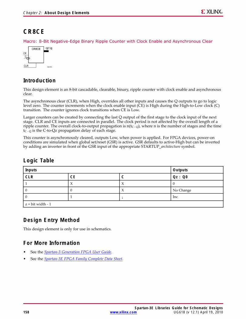
Chapter 2: About Design Elements
CR8CEMacro: 8-Bit Negative-Edge Binary Ripple Counter with Clock Enable and Asynchronous Clear
IntroductionThis design element is an 8-bit cascadable, clearable, binary, ripple counter with clock enable and asynchronousclear.
The asynchronous clear (CLR), when High, overrides all other inputs and causes the Q outputs to go to logiclevel zero. The counter increments when the clock enable input (CE) is High during the High-to-Low clock (C)transition. The counter ignores clock transitions when CE is Low.
Larger counters can be created by connecting the last Q output of the first stage to the clock input of the nextstage. CLR and CE inputs are connected in parallel. The clock period is not affected by the overall length of aripple counter. The overall clock-to-output propagation is n(tC - Q), where n is the number of stages and the timetC - Q is the C-to-Qz propagation delay of each stage.
This counter is asynchronously cleared, outputs Low, when power is applied. For FPGA devices, power-onconditions are simulated when global set/reset (GSR) is active. GSR defaults to active-High but can be invertedby adding an inverter in front of the GSR input of the appropriate STARTUP_architecture symbol.
Logic TableInputs Outputs
CLR CE C Qz : Q01 X X 0
0 0 X No Change
0 1 ↓ Inc
z = bit width - 1
Design Entry MethodThis design element is only for use in schematics.
For More Information• See the Spartan-3 Generation FPGA User Guide.
• See the Spartan-3E FPGA Family Complete Data Sheet.
Spartan-3E Libraries Guide for Schematic Designs158 www.xilinx.com UG618 (v 12.1) April 19, 2010
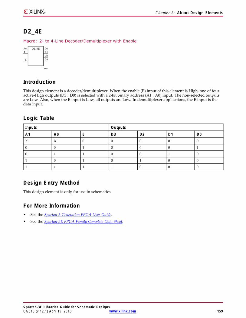
Chapter 2: About Design Elements
D2_4EMacro: 2- to 4-Line Decoder/Demultiplexer with Enable
IntroductionThis design element is a decoder/demultiplexer. When the enable (E) input of this element is High, one of fouractive-High outputs (D3 : D0) is selected with a 2-bit binary address (A1 : A0) input. The non-selected outputsare Low. Also, when the E input is Low, all outputs are Low. In demultiplexer applications, the E input is thedata input.
Logic TableInputs OutputsA1 A0 E D3 D2 D1 D0X X 0 0 0 0 0
0 0 1 0 0 0 1
0 1 1 0 0 1 0
1 0 1 0 1 0 0
1 1 1 1 0 0 0
Design Entry MethodThis design element is only for use in schematics.
For More Information• See the Spartan-3 Generation FPGA User Guide.
• See the Spartan-3E FPGA Family Complete Data Sheet.
Spartan-3E Libraries Guide for Schematic DesignsUG618 (v 12.1) April 19, 2010 www.xilinx.com 159
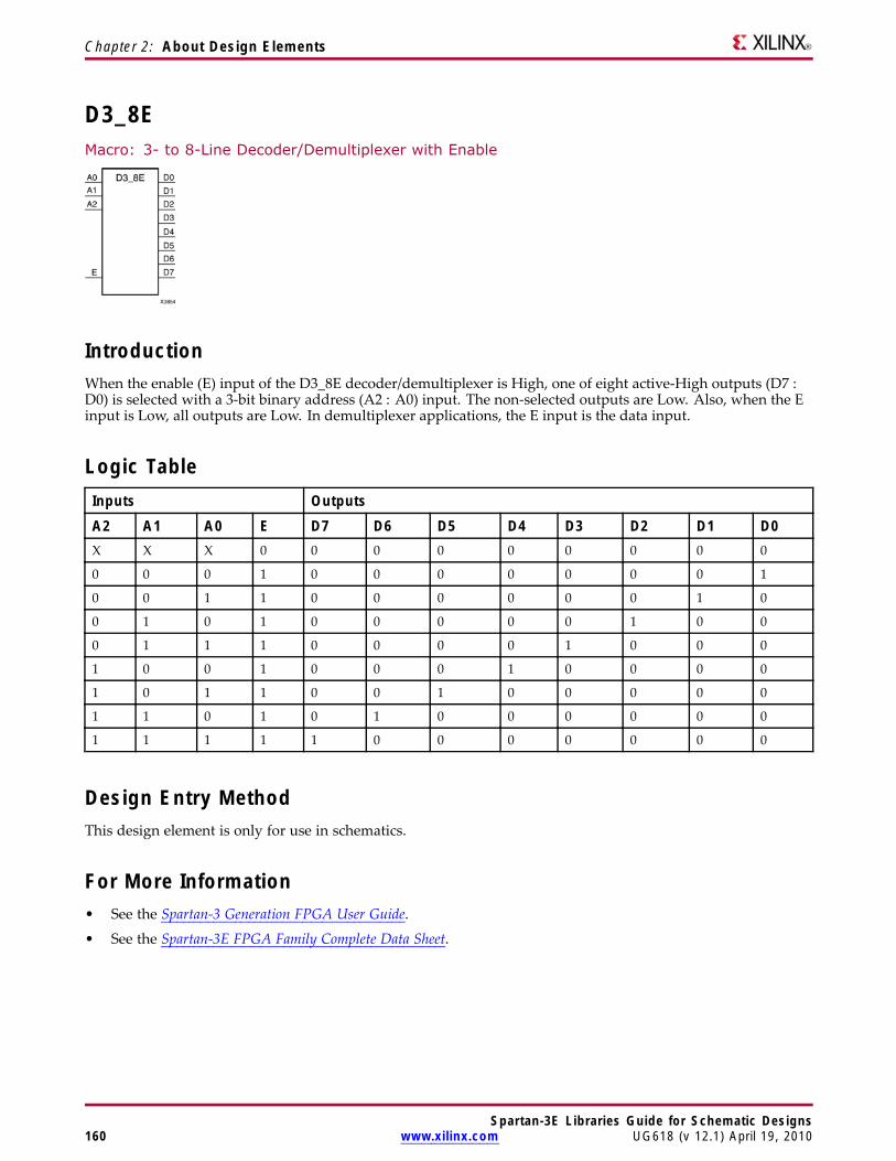
Chapter 2: About Design Elements
D3_8EMacro: 3- to 8-Line Decoder/Demultiplexer with Enable
IntroductionWhen the enable (E) input of the D3_8E decoder/demultiplexer is High, one of eight active-High outputs (D7 :D0) is selected with a 3-bit binary address (A2 : A0) input. The non-selected outputs are Low. Also, when the Einput is Low, all outputs are Low. In demultiplexer applications, the E input is the data input.
Logic TableInputs OutputsA2 A1 A0 E D7 D6 D5 D4 D3 D2 D1 D0X X X 0 0 0 0 0 0 0 0 0
0 0 0 1 0 0 0 0 0 0 0 1
0 0 1 1 0 0 0 0 0 0 1 0
0 1 0 1 0 0 0 0 0 1 0 0
0 1 1 1 0 0 0 0 1 0 0 0
1 0 0 1 0 0 0 1 0 0 0 0
1 0 1 1 0 0 1 0 0 0 0 0
1 1 0 1 0 1 0 0 0 0 0 0
1 1 1 1 1 0 0 0 0 0 0 0
Design Entry MethodThis design element is only for use in schematics.
For More Information• See the Spartan-3 Generation FPGA User Guide.
• See the Spartan-3E FPGA Family Complete Data Sheet.
Spartan-3E Libraries Guide for Schematic Designs160 www.xilinx.com UG618 (v 12.1) April 19, 2010
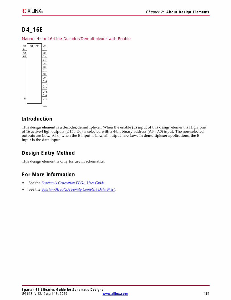
Chapter 2: About Design Elements
D4_16EMacro: 4- to 16-Line Decoder/Demultiplexer with Enable
IntroductionThis design element is a decoder/demultiplexer. When the enable (E) input of this design element is High, oneof 16 active-High outputs (D15 : D0) is selected with a 4-bit binary address (A3 : A0) input. The non-selectedoutputs are Low. Also, when the E input is Low, all outputs are Low. In demultiplexer applications, the Einput is the data input.
Design Entry MethodThis design element is only for use in schematics.
For More Information• See the Spartan-3 Generation FPGA User Guide.
• See the Spartan-3E FPGA Family Complete Data Sheet.
Spartan-3E Libraries Guide for Schematic DesignsUG618 (v 12.1) April 19, 2010 www.xilinx.com 161
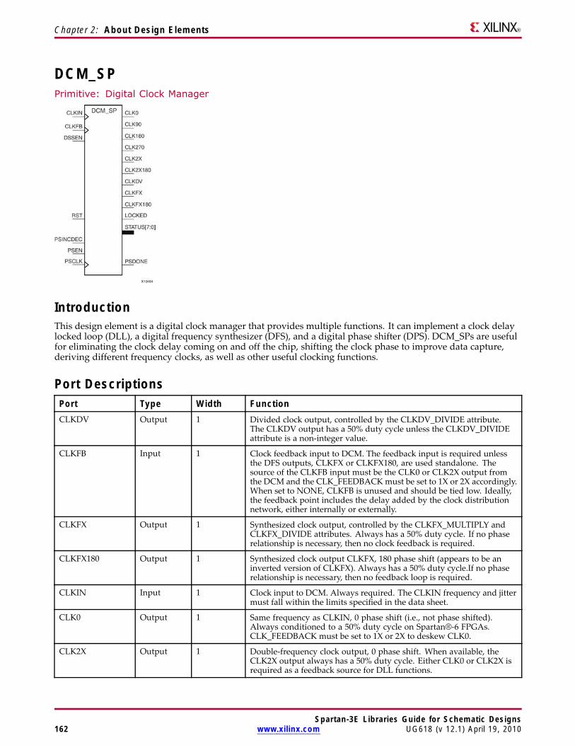
Chapter 2: About Design Elements
DCM_SPPrimitive: Digital Clock Manager
IntroductionThis design element is a digital clock manager that provides multiple functions. It can implement a clock delaylocked loop (DLL), a digital frequency synthesizer (DFS), and a digital phase shifter (DPS). DCM_SPs are usefulfor eliminating the clock delay coming on and off the chip, shifting the clock phase to improve data capture,deriving different frequency clocks, as well as other useful clocking functions.
Port DescriptionsPort Type Width FunctionCLKDV Output 1 Divided clock output, controlled by the CLKDV_DIVIDE attribute.
The CLKDV output has a 50% duty cycle unless the CLKDV_DIVIDEattribute is a non-integer value.
CLKFB Input 1 Clock feedback input to DCM. The feedback input is required unlessthe DFS outputs, CLKFX or CLKFX180, are used standalone. Thesource of the CLKFB input must be the CLK0 or CLK2X output fromthe DCM and the CLK_FEEDBACKmust be set to 1X or 2X accordingly.When set to NONE, CLKFB is unused and should be tied low. Ideally,the feedback point includes the delay added by the clock distributionnetwork, either internally or externally.
CLKFX Output 1 Synthesized clock output, controlled by the CLKFX_MULTIPLY andCLKFX_DIVIDE attributes. Always has a 50% duty cycle. If no phaserelationship is necessary, then no clock feedback is required.
CLKFX180 Output 1 Synthesized clock output CLKFX, 180 phase shift (appears to be aninverted version of CLKFX). Always has a 50% duty cycle.If no phaserelationship is necessary, then no feedback loop is required.
CLKIN Input 1 Clock input to DCM. Always required. The CLKIN frequency and jittermust fall within the limits specified in the data sheet.
CLK0 Output 1 Same frequency as CLKIN, 0 phase shift (i.e., not phase shifted).Always conditioned to a 50% duty cycle on Spartan®-6 FPGAs.CLK_FEEDBACK must be set to 1X or 2X to deskew CLK0.
CLK2X Output 1 Double-frequency clock output, 0 phase shift. When available, theCLK2X output always has a 50% duty cycle. Either CLK0 or CLK2X isrequired as a feedback source for DLL functions.
Spartan-3E Libraries Guide for Schematic Designs162 www.xilinx.com UG618 (v 12.1) April 19, 2010
Chapter 2: About Design Elements
Port Type Width FunctionCLK2X180 Output 1 Double-frequency clock output, 180 phase shift. When available, the
CLK2X180 output always has a 50% duty cycle.
CLK90 Output 1 Same frequency as CLKIN, 90 phase shift (quarter period). Alwaysconditioned to a 50% duty cycle on Spartan®-6 FPGAs.
CLK180 Output 1 Same frequency as CLKIN, 180 phase shift (half period). Alwaysconditioned to a 50% duty cycle on Spartan®-6 FPGAs.
CLK270 Output 1 Same frequency as CLKIN, 270 phase shift (three-quarters period).Always conditioned to a 50% duty cycle on Spartan®-6 FPGAs.
LOCKED Output 1 All DCM features have locked onto the CLKIN frequency. Clockoutputs are now valid, assuming CLKIN is within specified limits.
• 0 - DCM is attempting to lock onto CLKIN frequency. DCM clockoutputs are not valid.
• 1 - DCM is locked onto CLKIN frequency. DCM clock outputs arevalid.
• 1-to-0 - DCM lost lock. Reset DCM.
PSCLK Input 1 Clock input to variable phase shifter, clocked on rising edge. Whenusing a global clock buffer, only the upper eight BUFGMUXs candrive PSCLK: BUFGMUX_X2Y1, BUFGMUX_X2Y2, BUFGMUX_X2Y3,BUFGMUX_X2Y4, BUFGMUX_X3Y5, BUFGMUX_X3Y6,BUFGMUX_X3Y7 and BUFGMUX_X3Y8.
PSDONE Output 1 Variable phase shift operation complete.
• 0 - No phase shift operation is active or phase shift operation isin progress.
• 1 - Requested phase shift operation is complete. Output Highfor one PSCLK cycle. Next variable phase shift operation cancommence.
PSEN Input 1 Variable phase-shift enable. Can be inverted within a DCM block.Non-inverted behavior shown below.
• 0 - Disable variable phase shift. Ignore inputs to phase shifter.
• 1 - Enable variable phase shift operations on next rising PSCLKclock edge.
PSINCDEC Input 1 Increment/decrement variable phase shift. Can be inverted within aDCM block. Non-inverted behavior shown below.
• 0 - Decrement phase shift value on next enabled, rising PSCLKclock edge.
• 1 - Increment phase shift value on next enabled, rising PSCLK clockedge.
RST Input 1 Asynchronous reset input. Resets the DCM logic to its postconfigurationstate. Causes DCM to reacquire and relock to the CLKIN input.Invertible within DCM block. Non-inverted behavior shown below.
• 0 - No effect.
• 1 - Reset DCM block. Hold RST pulse High for at least three validCLKIN cycles.
Spartan-3E Libraries Guide for Schematic DesignsUG618 (v 12.1) April 19, 2010 www.xilinx.com 163
Chapter 2: About Design Elements
Port Type Width FunctionSTATUS[7:0] Output 8 The status output bus provides DCM status.
• STATUS[0] - Variable phase shift overflow. Control output forvariable fine phase shifting. The variable phase shifter has reacheda minimum or maximum limit value. The limit value is either+/-255 or a lesser value if the phase shift has reached the end ofthe delay line.
– 0 - The phase shift has not yet reached its limit value.
– 1 - The phase shift has reached its limited value.
• STATUS[1] - CLKIN Input Stopped Indicator. Available only whenthe CLKFB feedback input is connected. Held in reset until theLOCKED output is asserted. Requires at least one CLKIN cycle tobecome active. Never asserted if CLKIN never toggles.
– 0 - CLKIN input is toggling.
– 1 - CLKIN input is not toggling even though the locked outputcan still be High.
• STATUS[2] - CLKFX or CLKFX180 output stopped indicator.
– 0 - CLKFX and CLKFX180 outputs are toggling.
– 1 - CLKFX and CLKFX180 outputs are not toggling, eventhough the LOCKED output can still be High.
• STATUS[7:3] - Reserved.
Design Entry MethodThis design element can be used in schematics.
Available AttributesAttribute Type Allowed_Values Default DescriptionCLK_FEEDBACK String “1X”, “2X”,
“NONE”“1X” Defines the DCM feedbcak mode.
• 1X: CLK0 as feedback.
• 2X: CLK2X as feedback.
CLKDV_DIVIDE 1 significantdigit Float
2.0, 1.5, 2.5, 3.0,3.5, 4.0, 4.5, 5.0,5.5, 6.0, 6.5, 7.0,7.5, 8.0, 9.0, 10.0,11.0, 12.0, 13.0,14.0, 15.0, 16.0
2.0 Specifies the extent to which the CLKDLL,CLKDLLE, CLKDLLHF, or DCM_SPclock divider (CLKDV output) is to befrequency divided.
CLKFX_DIVIDE Integer 1 to 32 1 Specifies the frequency divider value forthe CLKFX output.
CLKFX_MULTIPLY Integer 2 to 32 4 Specifies the frequency multiplier valuefor the CLKFX output.
CLKIN_DIVIDE_BY_2
Boolean FALSE, TRUE FALSE Enables CLKIN divide by two features.
CLKIN_PERIOD String 0 bit String “10.0” Specifies the input period to the DCM_SPCLKIN input in ns.
Spartan-3E Libraries Guide for Schematic Designs164 www.xilinx.com UG618 (v 12.1) April 19, 2010
Chapter 2: About Design Elements
Attribute Type Allowed_Values Default DescriptionCLKOUT_PHASE_SHIFT
String “NONE”,“FIXED”,“VARIABLE”
“NONE” This attribute specifies the phase shiftmode.
• NONE: No phase shift capability.Any set value has no effect.
• FIXED: DCM outputs are a fixedphase shift from CLKIN. Value isspecified by PHASE_SHIFT attribute.
• VARIABLE: Allows the DCM outputsto be shifted in a positive and negativerange relative to CLKIN. Startingvalue is specified by PHASE_SHIFT.
DESKEW_ADJUST String “SYSTEM_SYNCHRONOUS”,“SOURCE_SYNCHRONOUS”
“SYSTEM_SYNCHRONOUS”
Sets configuration bits affecting the clockdelay alignment between the DCM_SPoutput clocks and an FPGA clock inputpin.
DFS_FREQUENCY_MODE
String “LOW”, “HIGH” “LOW” This is a legacy attribute. The DCM isalways in the automatic frequency searchmode. Setting High or Low makes noeffect.
DLL_FREQUENCY_MODE
String “LOW”, “HIGH” “LOW” This is a legacy attribute. The DCM isalways in the automatic frequency searchmode. Setting High or Low makes noeffect.
DSS_MODE String “NONE”,“SPREAD_2”,“SPREAD_4”,“SPREAD_6”,“SPREAD_8”
“NONE” Note Unused in Spartan®-6.
Specifies a frequency spread for outputclocks.
• NONE - The default, specifies nospread factors. The digital spreadspectrum function is disabled.
• SPREAD_2 - Creates a new clockperiod that is +/- 50 ps of the currentclock period
• SPREAD_4 - Creates a new clockperiod that is +/- 100 ps of the currentclock period.
• SPREAD_6 - Creates a new clockperiod that is +/- 150 ps of the currentclock period.
• SPREAD_8 - Creates a new clockperiod that is +/- 200 ps of the currentclock period.
The spreading is cumulative as theSPREAD_# is increased. For example,SPREAD_2 creates two additional clockfrequencies at +/-50 ps relative to theinput clock frequency; SPREAD_4 doesthe same as SPREAD_2, plus it createstwo additional clock frequencies at +/-100ps.
DUTY_CYCLE_CORRECTION
Boolean TRUE, FALSE TRUE Unsupported
FACTORY_JF Hexadecimal 16’h8080 to 16’hffff 16’hc080 Unsupported
Spartan-3E Libraries Guide for Schematic DesignsUG618 (v 12.1) April 19, 2010 www.xilinx.com 165
Chapter 2: About Design Elements
Attribute Type Allowed_Values Default DescriptionPHASE_SHIFT Integer -255 to 255 0 The PHASE_SHIFT attribute is applicable
only if the CLKOUT_PHASE_SHIFTattribute is set to FIXED or VARIABLE.Defines the rising-edge skew betweenCLKIN and all the DCM clock outputsat configuration and consequently phaseshifts the DCM clock outputs. Theskew or phase shift value is specifiedas an integer that represents a fractionof the clock period as expressed in theequations in Fine Phase Shifting. Actualallowable values depends on inputclock frequency. The actual range is lesswhen TCLKIN > FINE_SHIFT_RANGE.The FINE_SHIFT_RANGE specificationrepresents the total delay of all taps inthe delay line.
STARTUP_WAIT Boolean FALSE, TRUE FALSE Controls whether the FPGA configurationsignal DONE waits for the DCM to assertits LOCKED signal before going High.
• FALSE - Default. DONE is assertedat the end of configuration withoutwaiting for the DCM to assertLOCKED.
• TRUE - The DONE signal does nottransition High until the LOCKEDsignal transitions High on theassociated DCM.
STARTUP_WAIT does not preventLOCKED from transitioning High. TheFPGA startup sequence must also bemodified to insert a LCK (lock) cyclebefore the postponed cycle. The DONEcycle or the GWE cycle are typical choices.When more than one DCM is configured,the FPGA waits until all DCMs areLOCKED.
For More Information• See the Spartan-3 Generation FPGA User Guide.
• See the Spartan-3E FPGA Family Complete Data Sheet.
Spartan-3E Libraries Guide for Schematic Designs166 www.xilinx.com UG618 (v 12.1) April 19, 2010
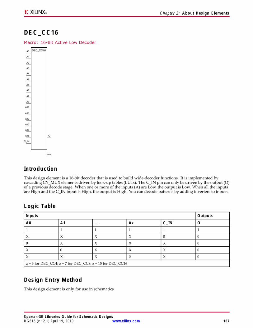
Chapter 2: About Design Elements
DEC_CC16Macro: 16-Bit Active Low Decoder
IntroductionThis design element is a 16-bit decoder that is used to build wide-decoder functions. It is implemented bycascading CY_MUX elements driven by look-up tables (LUTs). The C_IN pin can only be driven by the output (O)of a previous decode stage. When one or more of the inputs (A) are Low, the output is Low. When all the inputsare High and the C_IN input is High, the output is High. You can decode patterns by adding inverters to inputs.
Logic TableInputs Outputs
A0 A1 … Az C_IN O1 1 1 1 1 1
X X X X 0 0
0 X X X X 0
X 0 X X X 0
X X X 0 X 0
z = 3 for DEC_CC4; z = 7 for DEC_CC8; z = 15 for DEC_CC16
Design Entry MethodThis design element is only for use in schematics.
Spartan-3E Libraries Guide for Schematic DesignsUG618 (v 12.1) April 19, 2010 www.xilinx.com 167

Chapter 2: About Design Elements
For More Information• See the Spartan-3 Generation FPGA User Guide.
• See the Spartan-3E FPGA Family Complete Data Sheet.
Spartan-3E Libraries Guide for Schematic Designs168 www.xilinx.com UG618 (v 12.1) April 19, 2010
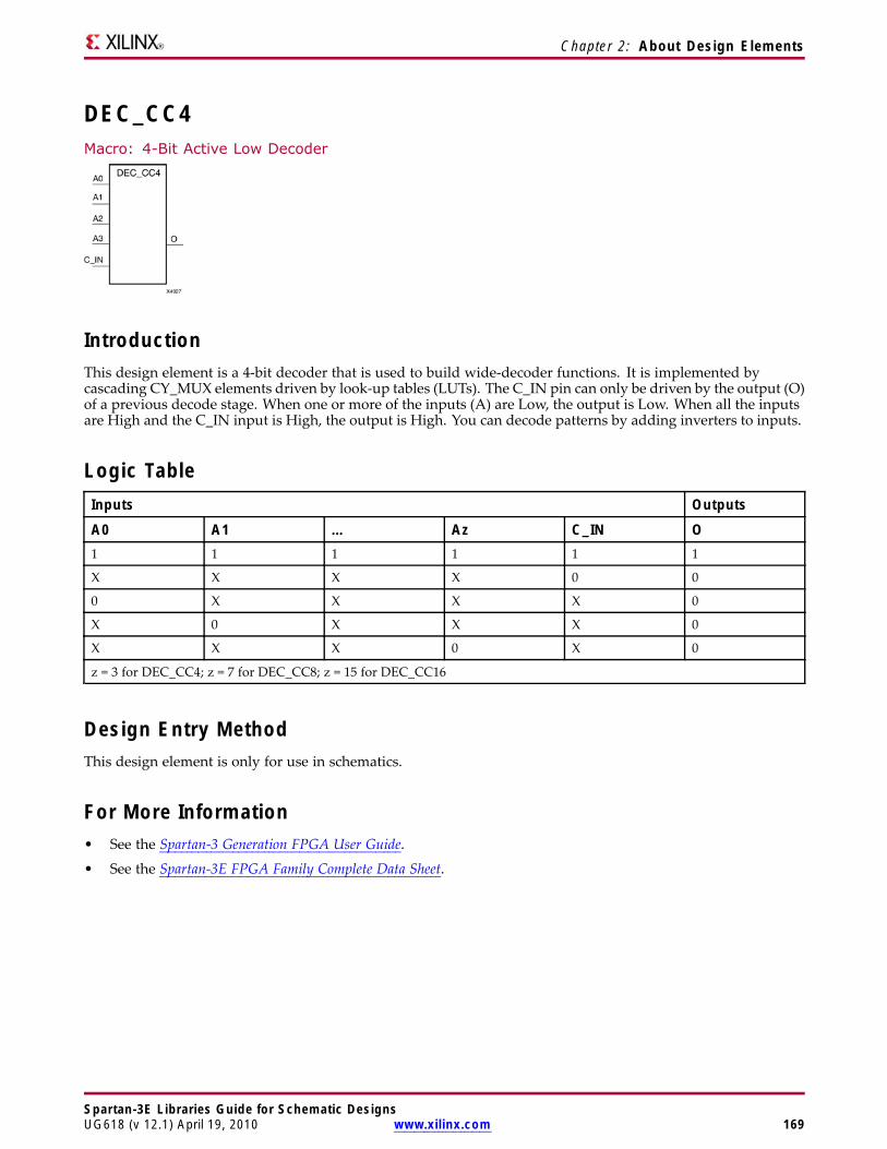
Chapter 2: About Design Elements
DEC_CC4Macro: 4-Bit Active Low Decoder
IntroductionThis design element is a 4-bit decoder that is used to build wide-decoder functions. It is implemented bycascading CY_MUX elements driven by look-up tables (LUTs). The C_IN pin can only be driven by the output (O)of a previous decode stage. When one or more of the inputs (A) are Low, the output is Low. When all the inputsare High and the C_IN input is High, the output is High. You can decode patterns by adding inverters to inputs.
Logic TableInputs Outputs
A0 A1 … Az C_IN O1 1 1 1 1 1
X X X X 0 0
0 X X X X 0
X 0 X X X 0
X X X 0 X 0
z = 3 for DEC_CC4; z = 7 for DEC_CC8; z = 15 for DEC_CC16
Design Entry MethodThis design element is only for use in schematics.
For More Information• See the Spartan-3 Generation FPGA User Guide.
• See the Spartan-3E FPGA Family Complete Data Sheet.
Spartan-3E Libraries Guide for Schematic DesignsUG618 (v 12.1) April 19, 2010 www.xilinx.com 169
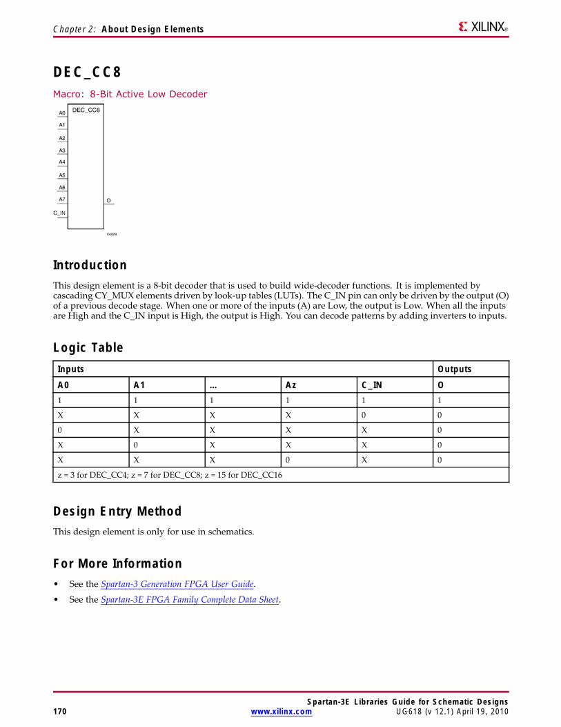
Chapter 2: About Design Elements
DEC_CC8Macro: 8-Bit Active Low Decoder
IntroductionThis design element is a 8-bit decoder that is used to build wide-decoder functions. It is implemented bycascading CY_MUX elements driven by look-up tables (LUTs). The C_IN pin can only be driven by the output (O)of a previous decode stage. When one or more of the inputs (A) are Low, the output is Low. When all the inputsare High and the C_IN input is High, the output is High. You can decode patterns by adding inverters to inputs.
Logic TableInputs Outputs
A0 A1 … Az C_IN O1 1 1 1 1 1
X X X X 0 0
0 X X X X 0
X 0 X X X 0
X X X 0 X 0
z = 3 for DEC_CC4; z = 7 for DEC_CC8; z = 15 for DEC_CC16
Design Entry MethodThis design element is only for use in schematics.
For More Information• See the Spartan-3 Generation FPGA User Guide.
• See the Spartan-3E FPGA Family Complete Data Sheet.
Spartan-3E Libraries Guide for Schematic Designs170 www.xilinx.com UG618 (v 12.1) April 19, 2010

Chapter 2: About Design Elements
DECODE16Macro: 16-Bit Active-Low Decoder
IntroductionThis design element is a 4-bit, active-low decoder that is implemented using combinations of LUTs and MUXCYs.
Logic TableInputs Outputs*
A0 A1 … Az O1 1 1 1 1
0 X X X 0
X 0 X X 0
X X X 0 0
z = bitwidth -1
*A pull-up resistor must be connected to the output to establish High-level drive current.
Design Entry MethodThis design element is only for use in schematics.
For More Information• See the Spartan-3 Generation FPGA User Guide.
• See the Spartan-3E FPGA Family Complete Data Sheet.
Spartan-3E Libraries Guide for Schematic DesignsUG618 (v 12.1) April 19, 2010 www.xilinx.com 171
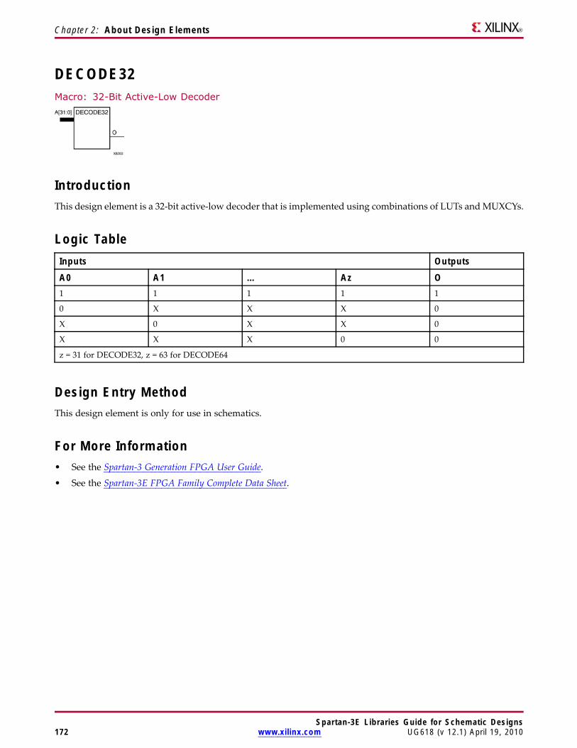
Chapter 2: About Design Elements
DECODE32Macro: 32-Bit Active-Low Decoder
IntroductionThis design element is a 32-bit active-low decoder that is implemented using combinations of LUTs andMUXCYs.
Logic TableInputs Outputs
A0 A1 … Az O1 1 1 1 1
0 X X X 0
X 0 X X 0
X X X 0 0
z = 31 for DECODE32, z = 63 for DECODE64
Design Entry MethodThis design element is only for use in schematics.
For More Information• See the Spartan-3 Generation FPGA User Guide.
• See the Spartan-3E FPGA Family Complete Data Sheet.
Spartan-3E Libraries Guide for Schematic Designs172 www.xilinx.com UG618 (v 12.1) April 19, 2010
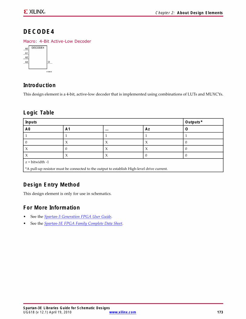
Chapter 2: About Design Elements
DECODE4Macro: 4-Bit Active-Low Decoder
IntroductionThis design element is a 4-bit, active-low decoder that is implemented using combinations of LUTs and MUXCYs.
Logic TableInputs Outputs*
A0 A1 … Az O1 1 1 1 1
0 X X X 0
X 0 X X 0
X X X 0 0
z = bitwidth -1
*A pull-up resistor must be connected to the output to establish High-level drive current.
Design Entry MethodThis design element is only for use in schematics.
For More Information• See the Spartan-3 Generation FPGA User Guide.
• See the Spartan-3E FPGA Family Complete Data Sheet.
Spartan-3E Libraries Guide for Schematic DesignsUG618 (v 12.1) April 19, 2010 www.xilinx.com 173
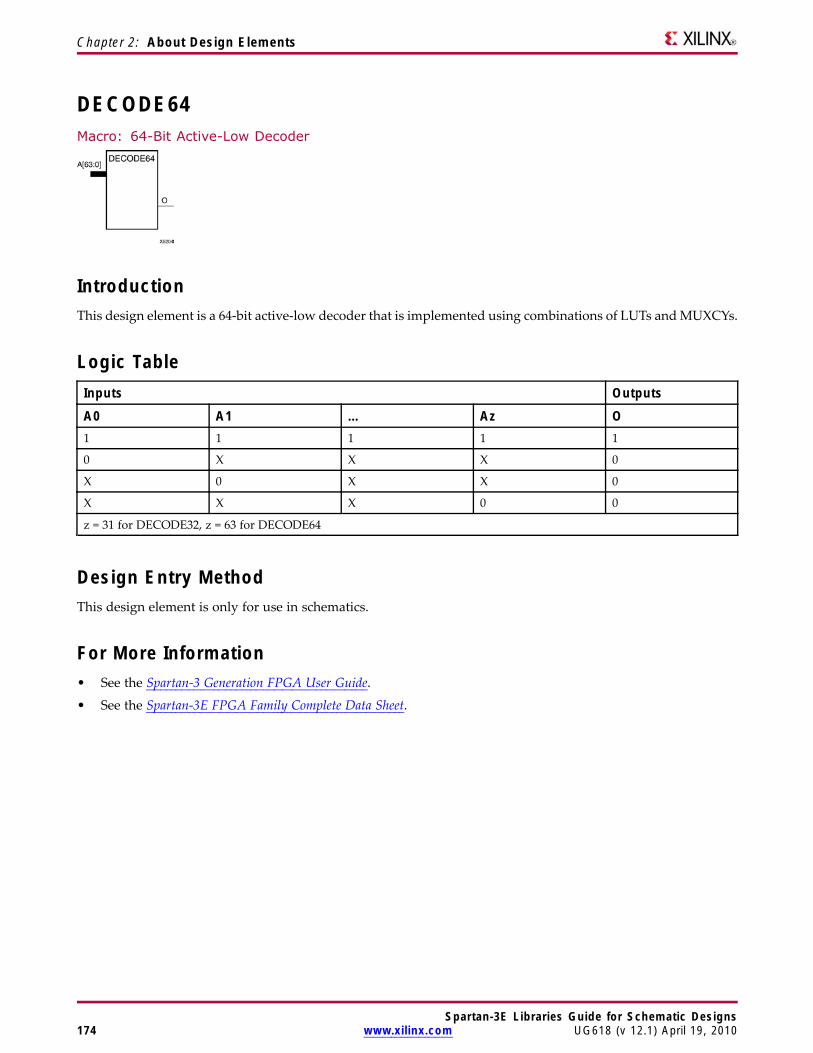
Chapter 2: About Design Elements
DECODE64Macro: 64-Bit Active-Low Decoder
IntroductionThis design element is a 64-bit active-low decoder that is implemented using combinations of LUTs andMUXCYs.
Logic TableInputs Outputs
A0 A1 … Az O1 1 1 1 1
0 X X X 0
X 0 X X 0
X X X 0 0
z = 31 for DECODE32, z = 63 for DECODE64
Design Entry MethodThis design element is only for use in schematics.
For More Information• See the Spartan-3 Generation FPGA User Guide.
• See the Spartan-3E FPGA Family Complete Data Sheet.
Spartan-3E Libraries Guide for Schematic Designs174 www.xilinx.com UG618 (v 12.1) April 19, 2010
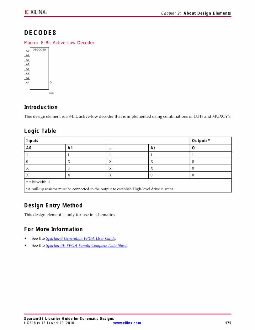
Chapter 2: About Design Elements
DECODE8Macro: 8-Bit Active-Low Decoder
IntroductionThis design element is a 8-bit, active-low decoder that is implemented using combinations of LUTs andMUXCY’s.
Logic TableInputs Outputs*
A0 A1 … Az O1 1 1 1 1
0 X X X 0
X 0 X X 0
X X X 0 0
z = bitwidth -1
*A pull-up resistor must be connected to the output to establish High-level drive current.
Design Entry MethodThis design element is only for use in schematics.
For More Information• See the Spartan-3 Generation FPGA User Guide.
• See the Spartan-3E FPGA Family Complete Data Sheet.
Spartan-3E Libraries Guide for Schematic DesignsUG618 (v 12.1) April 19, 2010 www.xilinx.com 175
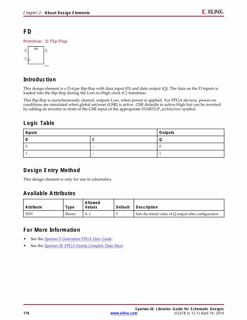
Chapter 2: About Design Elements
FDPrimitive: D Flip-Flop
IntroductionThis design element is a D-type flip-flop with data input (D) and data output (Q). The data on the D inputs isloaded into the flip-flop during the Low-to-High clock (C) transition.
This flip-flop is asynchronously cleared, outputs Low, when power is applied. For FPGA devices, power-onconditions are simulated when global set/reset (GSR) is active. GSR defaults to active-High but can be invertedby adding an inverter in front of the GSR input of the appropriate STARTUP_architecture symbol.
Logic TableInputs Outputs
D C Q0 ↑ 0
1 ↑ 1
Design Entry MethodThis design element is only for use in schematics.
Available Attributes
Attribute TypeAllowedValues Default Description
INIT Binary 0, 1 0 Sets the initial value of Q output after configuration
For More Information• See the Spartan-3 Generation FPGA User Guide.
• See the Spartan-3E FPGA Family Complete Data Sheet.
Spartan-3E Libraries Guide for Schematic Designs176 www.xilinx.com UG618 (v 12.1) April 19, 2010
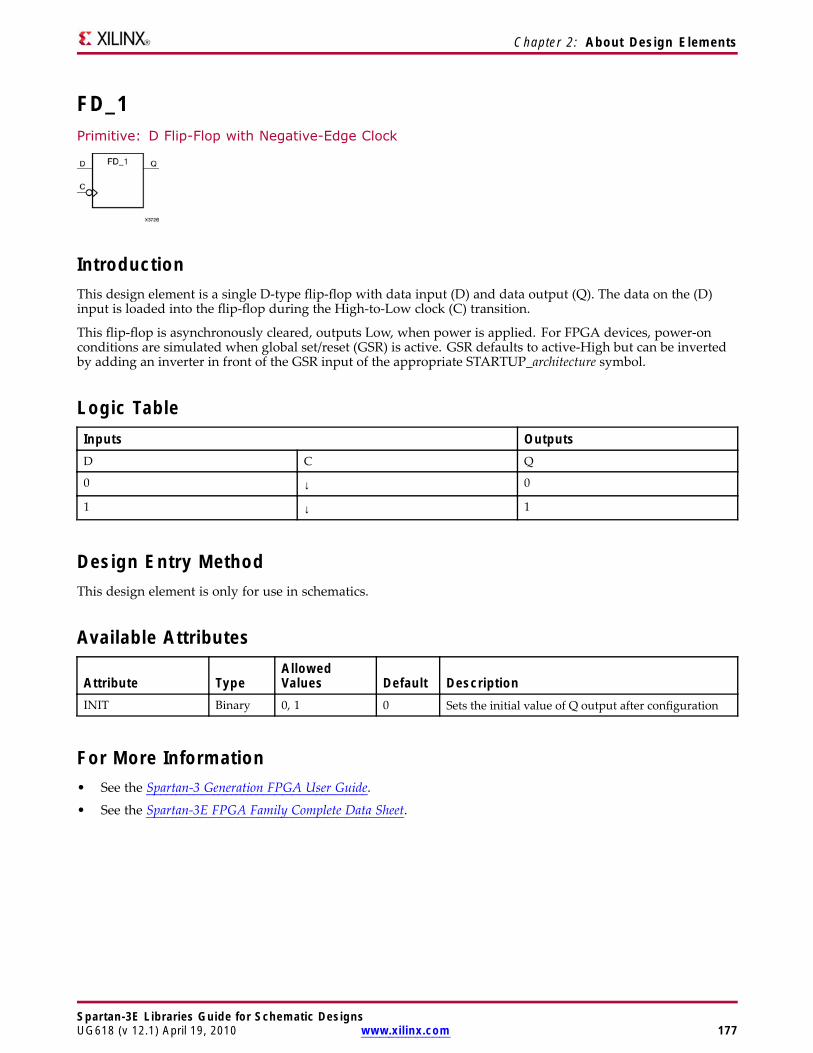
Chapter 2: About Design Elements
FD_1Primitive: D Flip-Flop with Negative-Edge Clock
IntroductionThis design element is a single D-type flip-flop with data input (D) and data output (Q). The data on the (D)input is loaded into the flip-flop during the High-to-Low clock (C) transition.
This flip-flop is asynchronously cleared, outputs Low, when power is applied. For FPGA devices, power-onconditions are simulated when global set/reset (GSR) is active. GSR defaults to active-High but can be invertedby adding an inverter in front of the GSR input of the appropriate STARTUP_architecture symbol.
Logic TableInputs OutputsD C Q
0 ↓ 0
1 ↓ 1
Design Entry MethodThis design element is only for use in schematics.
Available Attributes
Attribute TypeAllowedValues Default Description
INIT Binary 0, 1 0 Sets the initial value of Q output after configuration
For More Information• See the Spartan-3 Generation FPGA User Guide.
• See the Spartan-3E FPGA Family Complete Data Sheet.
Spartan-3E Libraries Guide for Schematic DesignsUG618 (v 12.1) April 19, 2010 www.xilinx.com 177
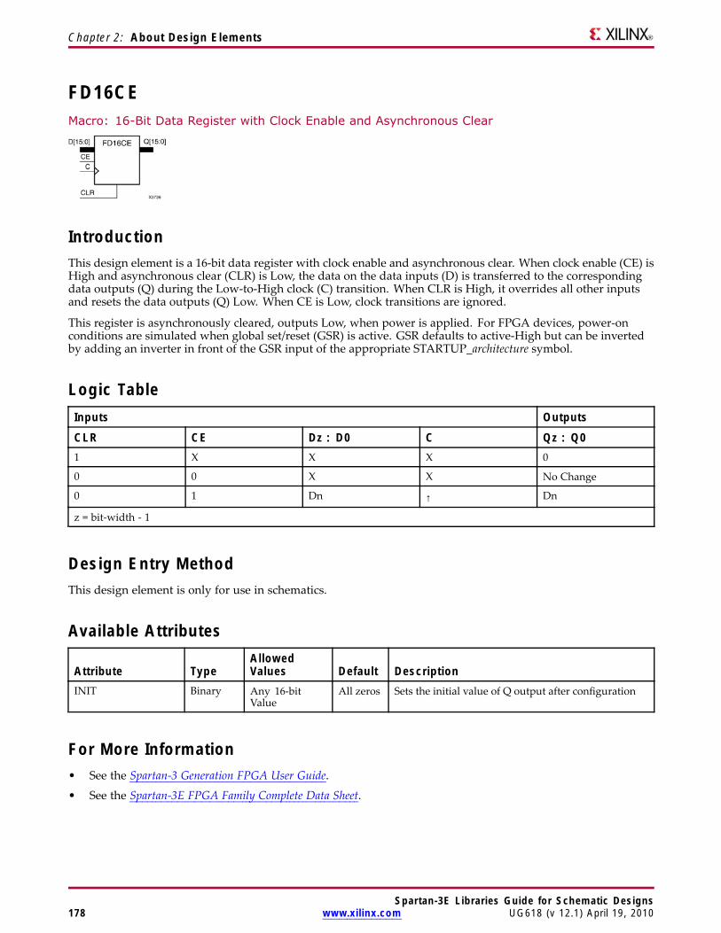
Chapter 2: About Design Elements
FD16CEMacro: 16-Bit Data Register with Clock Enable and Asynchronous Clear
IntroductionThis design element is a 16-bit data register with clock enable and asynchronous clear. When clock enable (CE) isHigh and asynchronous clear (CLR) is Low, the data on the data inputs (D) is transferred to the correspondingdata outputs (Q) during the Low-to-High clock (C) transition. When CLR is High, it overrides all other inputsand resets the data outputs (Q) Low. When CE is Low, clock transitions are ignored.
This register is asynchronously cleared, outputs Low, when power is applied. For FPGA devices, power-onconditions are simulated when global set/reset (GSR) is active. GSR defaults to active-High but can be invertedby adding an inverter in front of the GSR input of the appropriate STARTUP_architecture symbol.
Logic TableInputs Outputs
CLR CE Dz : D0 C Qz : Q01 X X X 0
0 0 X X No Change
0 1 Dn ↑ Dn
z = bit-width - 1
Design Entry MethodThis design element is only for use in schematics.
Available Attributes
Attribute TypeAllowedValues Default Description
INIT Binary Any 16-bitValue
All zeros Sets the initial value of Q output after configuration
For More Information• See the Spartan-3 Generation FPGA User Guide.
• See the Spartan-3E FPGA Family Complete Data Sheet.
Spartan-3E Libraries Guide for Schematic Designs178 www.xilinx.com UG618 (v 12.1) April 19, 2010
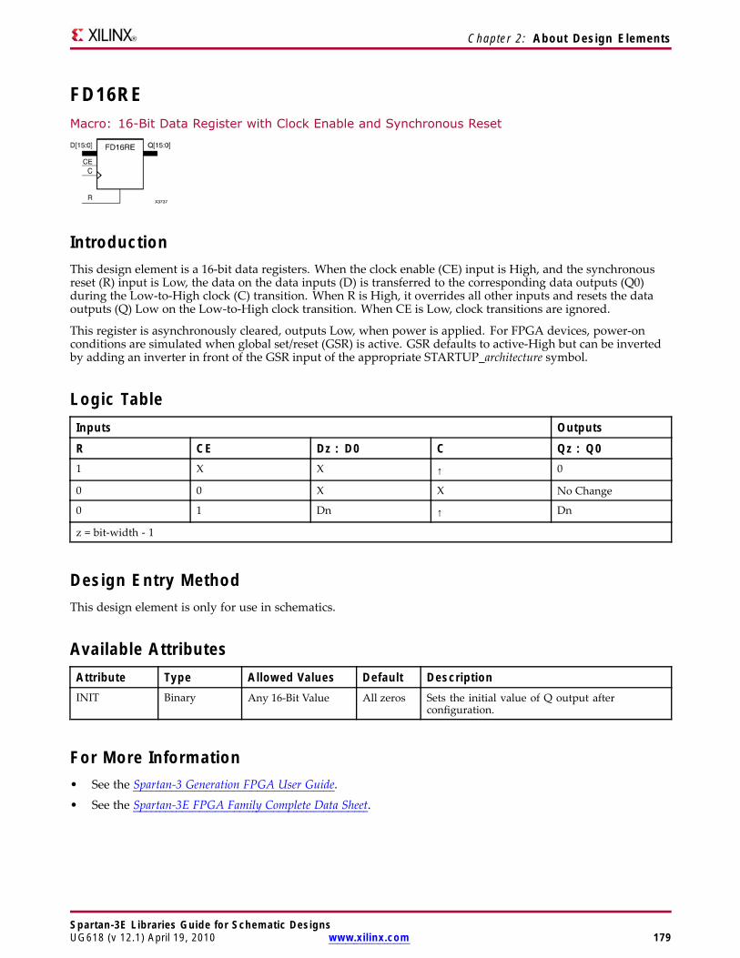
Chapter 2: About Design Elements
FD16REMacro: 16-Bit Data Register with Clock Enable and Synchronous Reset
IntroductionThis design element is a 16-bit data registers. When the clock enable (CE) input is High, and the synchronousreset (R) input is Low, the data on the data inputs (D) is transferred to the corresponding data outputs (Q0)during the Low-to-High clock (C) transition. When R is High, it overrides all other inputs and resets the dataoutputs (Q) Low on the Low-to-High clock transition. When CE is Low, clock transitions are ignored.
This register is asynchronously cleared, outputs Low, when power is applied. For FPGA devices, power-onconditions are simulated when global set/reset (GSR) is active. GSR defaults to active-High but can be invertedby adding an inverter in front of the GSR input of the appropriate STARTUP_architecture symbol.
Logic TableInputs Outputs
R CE Dz : D0 C Qz : Q01 X X ↑ 0
0 0 X X No Change
0 1 Dn ↑ Dn
z = bit-width - 1
Design Entry MethodThis design element is only for use in schematics.
Available AttributesAttribute Type Allowed Values Default DescriptionINIT Binary Any 16-Bit Value All zeros Sets the initial value of Q output after
configuration.
For More Information• See the Spartan-3 Generation FPGA User Guide.
• See the Spartan-3E FPGA Family Complete Data Sheet.
Spartan-3E Libraries Guide for Schematic DesignsUG618 (v 12.1) April 19, 2010 www.xilinx.com 179
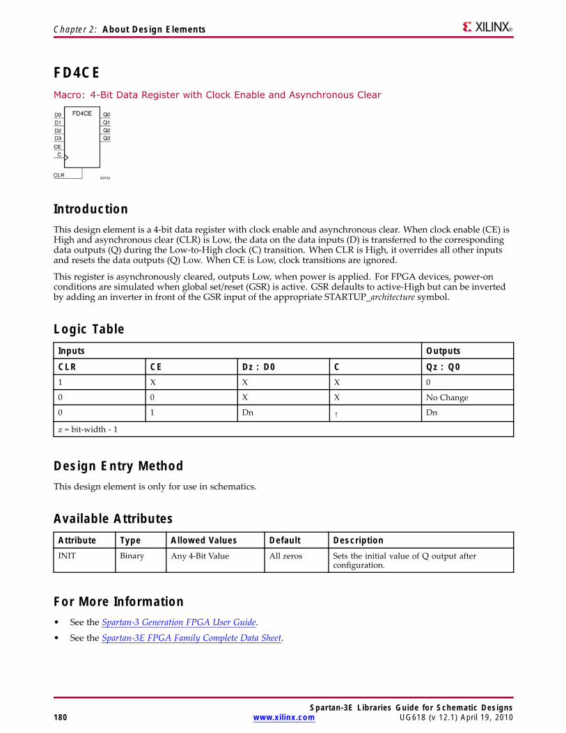
Chapter 2: About Design Elements
FD4CEMacro: 4-Bit Data Register with Clock Enable and Asynchronous Clear
IntroductionThis design element is a 4-bit data register with clock enable and asynchronous clear. When clock enable (CE) isHigh and asynchronous clear (CLR) is Low, the data on the data inputs (D) is transferred to the correspondingdata outputs (Q) during the Low-to-High clock (C) transition. When CLR is High, it overrides all other inputsand resets the data outputs (Q) Low. When CE is Low, clock transitions are ignored.
This register is asynchronously cleared, outputs Low, when power is applied. For FPGA devices, power-onconditions are simulated when global set/reset (GSR) is active. GSR defaults to active-High but can be invertedby adding an inverter in front of the GSR input of the appropriate STARTUP_architecture symbol.
Logic TableInputs Outputs
CLR CE Dz : D0 C Qz : Q01 X X X 0
0 0 X X No Change
0 1 Dn ↑ Dn
z = bit-width - 1
Design Entry MethodThis design element is only for use in schematics.
Available AttributesAttribute Type Allowed Values Default DescriptionINIT Binary Any 4-Bit Value All zeros Sets the initial value of Q output after
configuration.
For More Information• See the Spartan-3 Generation FPGA User Guide.
• See the Spartan-3E FPGA Family Complete Data Sheet.
Spartan-3E Libraries Guide for Schematic Designs180 www.xilinx.com UG618 (v 12.1) April 19, 2010
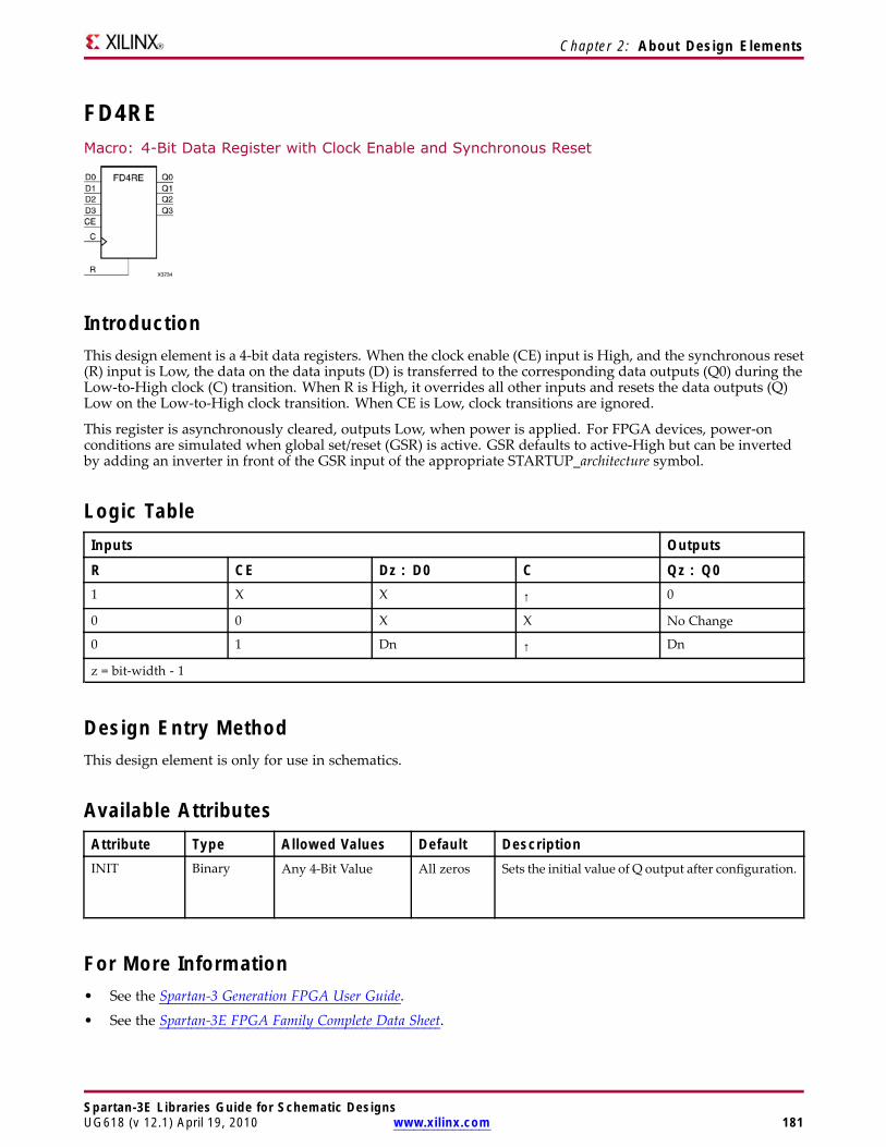
Chapter 2: About Design Elements
FD4REMacro: 4-Bit Data Register with Clock Enable and Synchronous Reset
IntroductionThis design element is a 4-bit data registers. When the clock enable (CE) input is High, and the synchronous reset(R) input is Low, the data on the data inputs (D) is transferred to the corresponding data outputs (Q0) during theLow-to-High clock (C) transition. When R is High, it overrides all other inputs and resets the data outputs (Q)Low on the Low-to-High clock transition. When CE is Low, clock transitions are ignored.
This register is asynchronously cleared, outputs Low, when power is applied. For FPGA devices, power-onconditions are simulated when global set/reset (GSR) is active. GSR defaults to active-High but can be invertedby adding an inverter in front of the GSR input of the appropriate STARTUP_architecture symbol.
Logic TableInputs Outputs
R CE Dz : D0 C Qz : Q01 X X ↑ 0
0 0 X X No Change
0 1 Dn ↑ Dn
z = bit-width - 1
Design Entry MethodThis design element is only for use in schematics.
Available AttributesAttribute Type Allowed Values Default DescriptionINIT Binary Any 4-Bit Value All zeros Sets the initial value of Q output after configuration.
For More Information• See the Spartan-3 Generation FPGA User Guide.
• See the Spartan-3E FPGA Family Complete Data Sheet.
Spartan-3E Libraries Guide for Schematic DesignsUG618 (v 12.1) April 19, 2010 www.xilinx.com 181
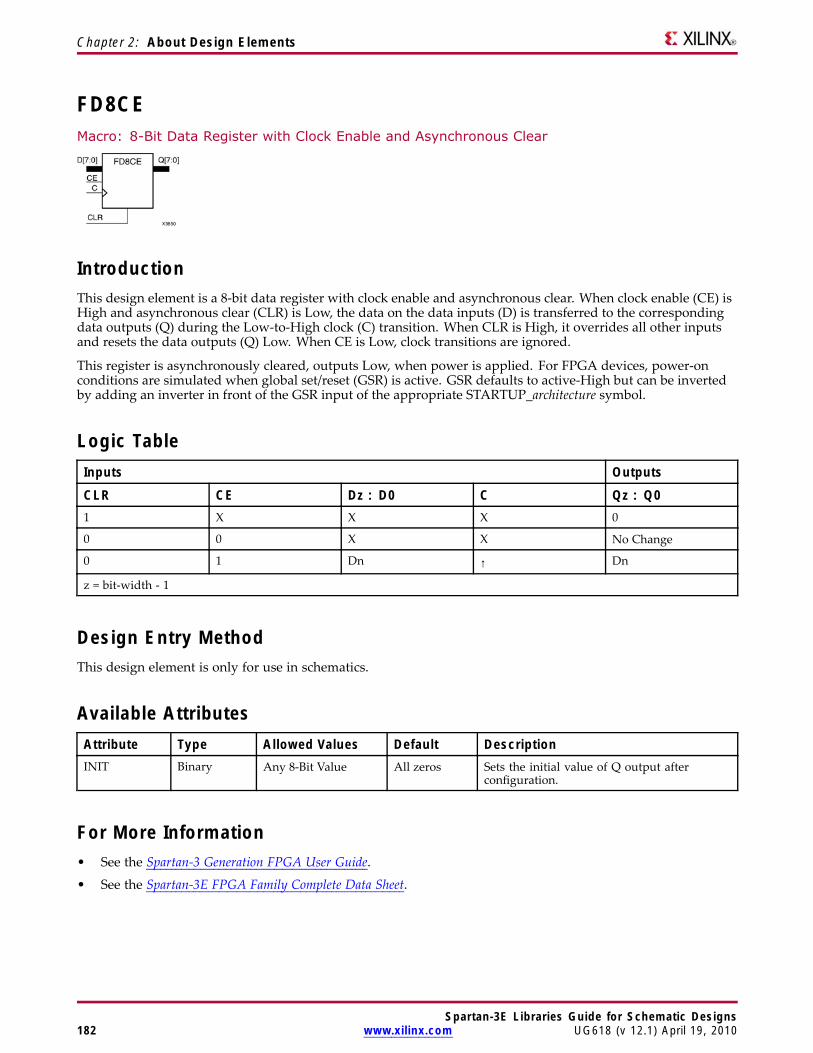
Chapter 2: About Design Elements
FD8CEMacro: 8-Bit Data Register with Clock Enable and Asynchronous Clear
IntroductionThis design element is a 8-bit data register with clock enable and asynchronous clear. When clock enable (CE) isHigh and asynchronous clear (CLR) is Low, the data on the data inputs (D) is transferred to the correspondingdata outputs (Q) during the Low-to-High clock (C) transition. When CLR is High, it overrides all other inputsand resets the data outputs (Q) Low. When CE is Low, clock transitions are ignored.
This register is asynchronously cleared, outputs Low, when power is applied. For FPGA devices, power-onconditions are simulated when global set/reset (GSR) is active. GSR defaults to active-High but can be invertedby adding an inverter in front of the GSR input of the appropriate STARTUP_architecture symbol.
Logic TableInputs Outputs
CLR CE Dz : D0 C Qz : Q01 X X X 0
0 0 X X No Change
0 1 Dn ↑ Dn
z = bit-width - 1
Design Entry MethodThis design element is only for use in schematics.
Available AttributesAttribute Type Allowed Values Default DescriptionINIT Binary Any 8-Bit Value All zeros Sets the initial value of Q output after
configuration.
For More Information• See the Spartan-3 Generation FPGA User Guide.
• See the Spartan-3E FPGA Family Complete Data Sheet.
Spartan-3E Libraries Guide for Schematic Designs182 www.xilinx.com UG618 (v 12.1) April 19, 2010
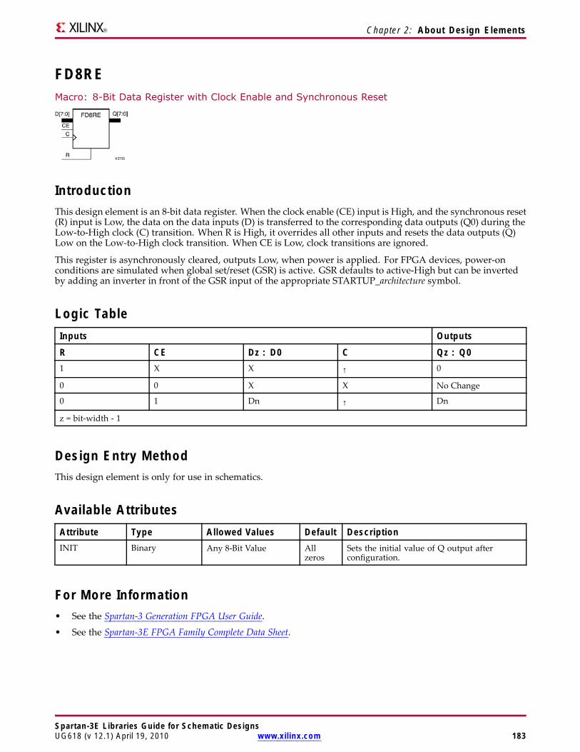
Chapter 2: About Design Elements
FD8REMacro: 8-Bit Data Register with Clock Enable and Synchronous Reset
IntroductionThis design element is an 8-bit data register. When the clock enable (CE) input is High, and the synchronous reset(R) input is Low, the data on the data inputs (D) is transferred to the corresponding data outputs (Q0) during theLow-to-High clock (C) transition. When R is High, it overrides all other inputs and resets the data outputs (Q)Low on the Low-to-High clock transition. When CE is Low, clock transitions are ignored.
This register is asynchronously cleared, outputs Low, when power is applied. For FPGA devices, power-onconditions are simulated when global set/reset (GSR) is active. GSR defaults to active-High but can be invertedby adding an inverter in front of the GSR input of the appropriate STARTUP_architecture symbol.
Logic TableInputs Outputs
R CE Dz : D0 C Qz : Q01 X X ↑ 0
0 0 X X No Change
0 1 Dn ↑ Dn
z = bit-width - 1
Design Entry MethodThis design element is only for use in schematics.
Available AttributesAttribute Type Allowed Values Default DescriptionINIT Binary Any 8-Bit Value All
zerosSets the initial value of Q output afterconfiguration.
For More Information• See the Spartan-3 Generation FPGA User Guide.
• See the Spartan-3E FPGA Family Complete Data Sheet.
Spartan-3E Libraries Guide for Schematic DesignsUG618 (v 12.1) April 19, 2010 www.xilinx.com 183
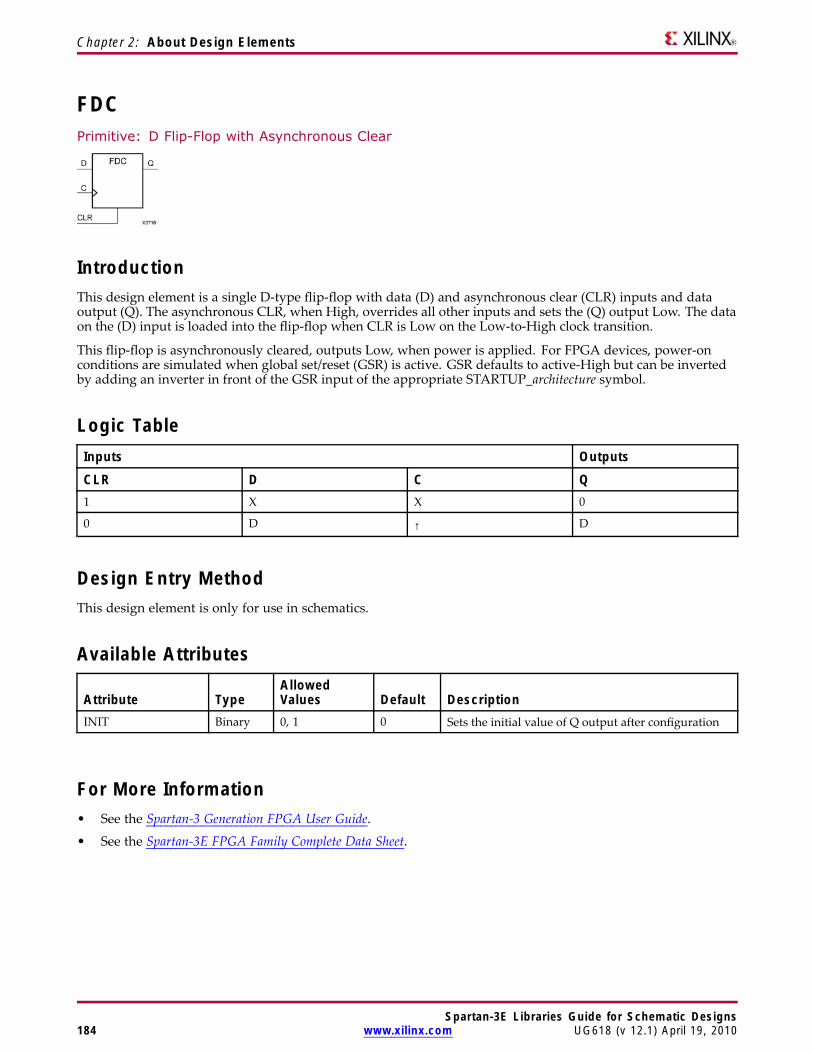
Chapter 2: About Design Elements
FDCPrimitive: D Flip-Flop with Asynchronous Clear
IntroductionThis design element is a single D-type flip-flop with data (D) and asynchronous clear (CLR) inputs and dataoutput (Q). The asynchronous CLR, when High, overrides all other inputs and sets the (Q) output Low. The dataon the (D) input is loaded into the flip-flop when CLR is Low on the Low-to-High clock transition.
This flip-flop is asynchronously cleared, outputs Low, when power is applied. For FPGA devices, power-onconditions are simulated when global set/reset (GSR) is active. GSR defaults to active-High but can be invertedby adding an inverter in front of the GSR input of the appropriate STARTUP_architecture symbol.
Logic TableInputs Outputs
CLR D C Q1 X X 0
0 D ↑ D
Design Entry MethodThis design element is only for use in schematics.
Available Attributes
Attribute TypeAllowedValues Default Description
INIT Binary 0, 1 0 Sets the initial value of Q output after configuration
For More Information• See the Spartan-3 Generation FPGA User Guide.
• See the Spartan-3E FPGA Family Complete Data Sheet.
Spartan-3E Libraries Guide for Schematic Designs184 www.xilinx.com UG618 (v 12.1) April 19, 2010
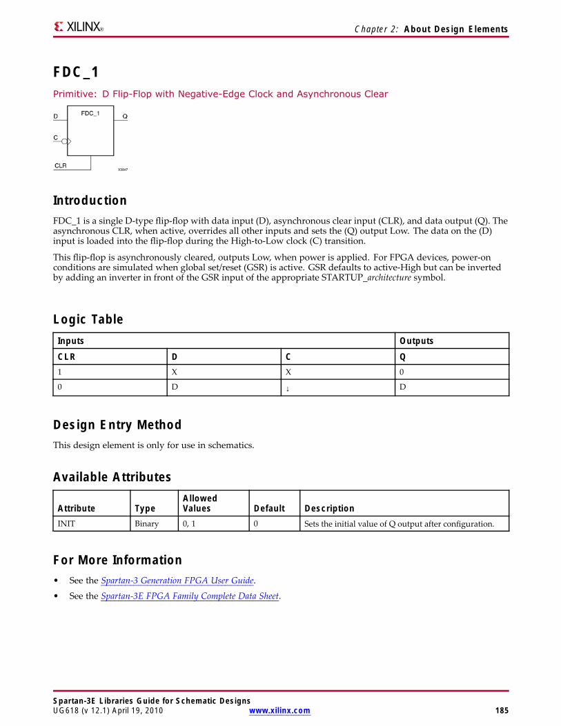
Chapter 2: About Design Elements
FDC_1Primitive: D Flip-Flop with Negative-Edge Clock and Asynchronous Clear
IntroductionFDC_1 is a single D-type flip-flop with data input (D), asynchronous clear input (CLR), and data output (Q). Theasynchronous CLR, when active, overrides all other inputs and sets the (Q) output Low. The data on the (D)input is loaded into the flip-flop during the High-to-Low clock (C) transition.
This flip-flop is asynchronously cleared, outputs Low, when power is applied. For FPGA devices, power-onconditions are simulated when global set/reset (GSR) is active. GSR defaults to active-High but can be invertedby adding an inverter in front of the GSR input of the appropriate STARTUP_architecture symbol.
Logic TableInputs Outputs
CLR D C Q1 X X 0
0 D ↓ D
Design Entry MethodThis design element is only for use in schematics.
Available Attributes
Attribute TypeAllowedValues Default Description
INIT Binary 0, 1 0 Sets the initial value of Q output after configuration.
For More Information• See the Spartan-3 Generation FPGA User Guide.
• See the Spartan-3E FPGA Family Complete Data Sheet.
Spartan-3E Libraries Guide for Schematic DesignsUG618 (v 12.1) April 19, 2010 www.xilinx.com 185
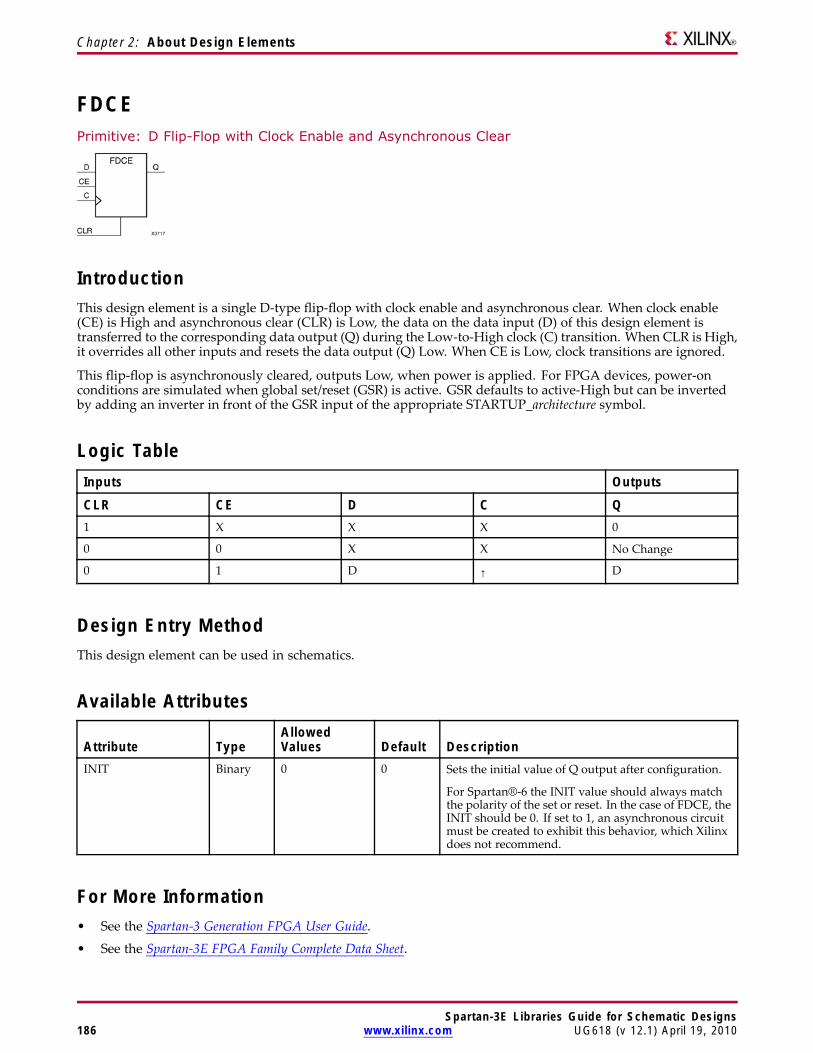
Chapter 2: About Design Elements
FDCEPrimitive: D Flip-Flop with Clock Enable and Asynchronous Clear
IntroductionThis design element is a single D-type flip-flop with clock enable and asynchronous clear. When clock enable(CE) is High and asynchronous clear (CLR) is Low, the data on the data input (D) of this design element istransferred to the corresponding data output (Q) during the Low-to-High clock (C) transition. When CLR is High,it overrides all other inputs and resets the data output (Q) Low. When CE is Low, clock transitions are ignored.
This flip-flop is asynchronously cleared, outputs Low, when power is applied. For FPGA devices, power-onconditions are simulated when global set/reset (GSR) is active. GSR defaults to active-High but can be invertedby adding an inverter in front of the GSR input of the appropriate STARTUP_architecture symbol.
Logic TableInputs Outputs
CLR CE D C Q1 X X X 0
0 0 X X No Change
0 1 D ↑ D
Design Entry MethodThis design element can be used in schematics.
Available Attributes
Attribute TypeAllowedValues Default Description
INIT Binary 0 0 Sets the initial value of Q output after configuration.
For Spartan®-6 the INIT value should always matchthe polarity of the set or reset. In the case of FDCE, theINIT should be 0. If set to 1, an asynchronous circuitmust be created to exhibit this behavior, which Xilinxdoes not recommend.
For More Information• See the Spartan-3 Generation FPGA User Guide.
• See the Spartan-3E FPGA Family Complete Data Sheet.
Spartan-3E Libraries Guide for Schematic Designs186 www.xilinx.com UG618 (v 12.1) April 19, 2010
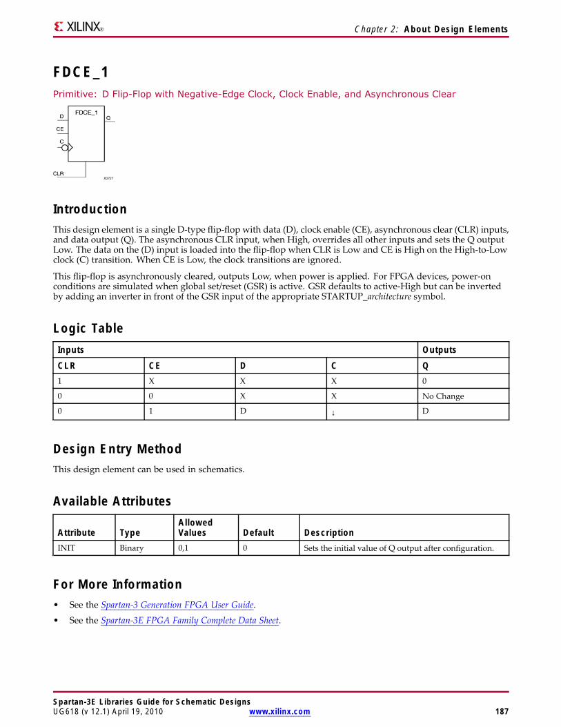
Chapter 2: About Design Elements
FDCE_1Primitive: D Flip-Flop with Negative-Edge Clock, Clock Enable, and Asynchronous Clear
IntroductionThis design element is a single D-type flip-flop with data (D), clock enable (CE), asynchronous clear (CLR) inputs,and data output (Q). The asynchronous CLR input, when High, overrides all other inputs and sets the Q outputLow. The data on the (D) input is loaded into the flip-flop when CLR is Low and CE is High on the High-to-Lowclock (C) transition. When CE is Low, the clock transitions are ignored.
This flip-flop is asynchronously cleared, outputs Low, when power is applied. For FPGA devices, power-onconditions are simulated when global set/reset (GSR) is active. GSR defaults to active-High but can be invertedby adding an inverter in front of the GSR input of the appropriate STARTUP_architecture symbol.
Logic TableInputs Outputs
CLR CE D C Q1 X X X 0
0 0 X X No Change
0 1 D ↓ D
Design Entry MethodThis design element can be used in schematics.
Available Attributes
Attribute TypeAllowedValues Default Description
INIT Binary 0,1 0 Sets the initial value of Q output after configuration.
For More Information• See the Spartan-3 Generation FPGA User Guide.
• See the Spartan-3E FPGA Family Complete Data Sheet.
Spartan-3E Libraries Guide for Schematic DesignsUG618 (v 12.1) April 19, 2010 www.xilinx.com 187
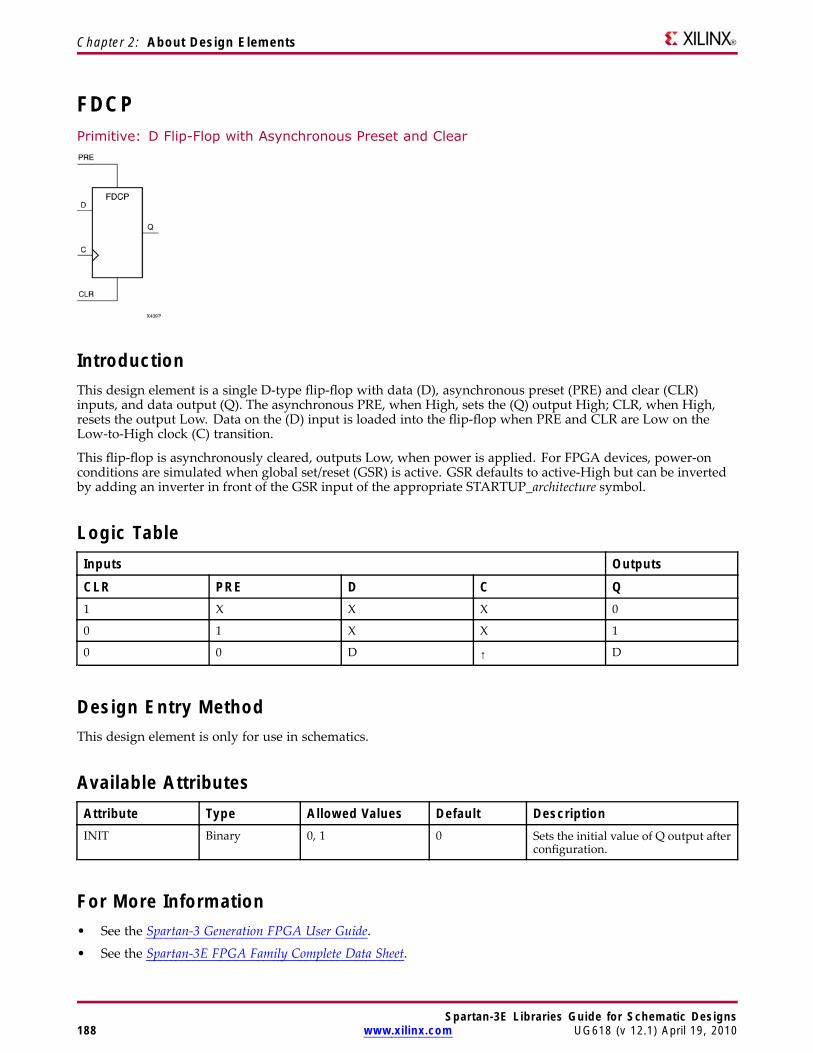
Chapter 2: About Design Elements
FDCPPrimitive: D Flip-Flop with Asynchronous Preset and Clear
IntroductionThis design element is a single D-type flip-flop with data (D), asynchronous preset (PRE) and clear (CLR)inputs, and data output (Q). The asynchronous PRE, when High, sets the (Q) output High; CLR, when High,resets the output Low. Data on the (D) input is loaded into the flip-flop when PRE and CLR are Low on theLow-to-High clock (C) transition.
This flip-flop is asynchronously cleared, outputs Low, when power is applied. For FPGA devices, power-onconditions are simulated when global set/reset (GSR) is active. GSR defaults to active-High but can be invertedby adding an inverter in front of the GSR input of the appropriate STARTUP_architecture symbol.
Logic TableInputs Outputs
CLR PRE D C Q1 X X X 0
0 1 X X 1
0 0 D ↑ D
Design Entry MethodThis design element is only for use in schematics.
Available AttributesAttribute Type Allowed Values Default DescriptionINIT Binary 0, 1 0 Sets the initial value of Q output after
configuration.
For More Information• See the Spartan-3 Generation FPGA User Guide.
• See the Spartan-3E FPGA Family Complete Data Sheet.
Spartan-3E Libraries Guide for Schematic Designs188 www.xilinx.com UG618 (v 12.1) April 19, 2010
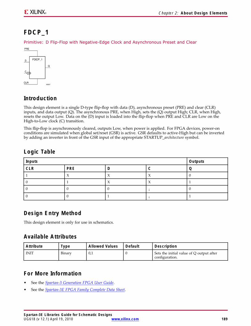
Chapter 2: About Design Elements
FDCP_1Primitive: D Flip-Flop with Negative-Edge Clock and Asynchronous Preset and Clear
IntroductionThis design element is a single D-type flip-flop with data (D), asynchronous preset (PRE) and clear (CLR)inputs, and data output (Q). The asynchronous PRE, when High, sets the (Q) output High; CLR, when High,resets the output Low. Data on the (D) input is loaded into the flip-flop when PRE and CLR are Low on theHigh-to-Low clock (C) transition.
This flip-flop is asynchronously cleared, outputs Low, when power is applied. For FPGA devices, power-onconditions are simulated when global set/reset (GSR) is active. GSR defaults to active-High but can be invertedby adding an inverter in front of the GSR input of the appropriate STARTUP_architecture symbol.
Logic TableInputs Outputs
CLR PRE D C Q1 X X X 0
0 1 X X 1
0 0 0 ↓ 0
0 0 1 ↓ 1
Design Entry MethodThis design element is only for use in schematics.
Available AttributesAttribute Type Allowed Values Default DescriptionINIT Binary 0,1 0 Sets the initial value of Q output after
configuration.
For More Information• See the Spartan-3 Generation FPGA User Guide.
• See the Spartan-3E FPGA Family Complete Data Sheet.
Spartan-3E Libraries Guide for Schematic DesignsUG618 (v 12.1) April 19, 2010 www.xilinx.com 189
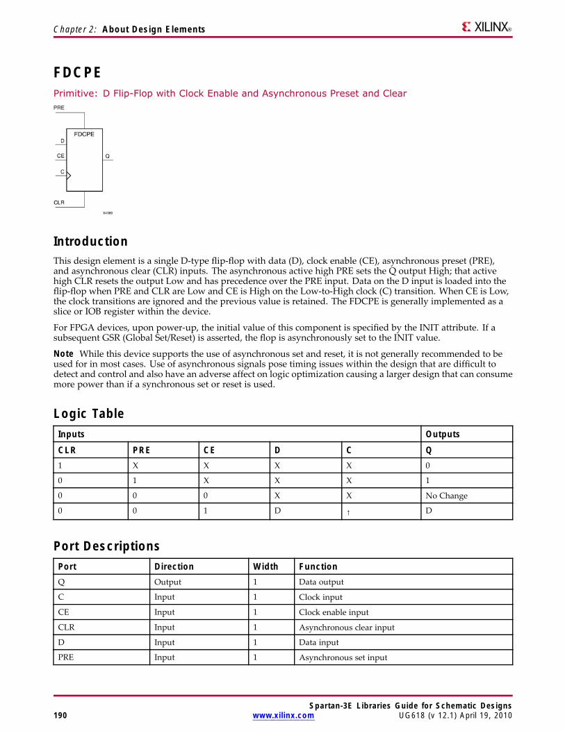
Chapter 2: About Design Elements
FDCPEPrimitive: D Flip-Flop with Clock Enable and Asynchronous Preset and Clear
IntroductionThis design element is a single D-type flip-flop with data (D), clock enable (CE), asynchronous preset (PRE),and asynchronous clear (CLR) inputs. The asynchronous active high PRE sets the Q output High; that activehigh CLR resets the output Low and has precedence over the PRE input. Data on the D input is loaded into theflip-flop when PRE and CLR are Low and CE is High on the Low-to-High clock (C) transition. When CE is Low,the clock transitions are ignored and the previous value is retained. The FDCPE is generally implemented as aslice or IOB register within the device.
For FPGA devices, upon power-up, the initial value of this component is specified by the INIT attribute. If asubsequent GSR (Global Set/Reset) is asserted, the flop is asynchronously set to the INIT value.
Note While this device supports the use of asynchronous set and reset, it is not generally recommended to beused for in most cases. Use of asynchronous signals pose timing issues within the design that are difficult todetect and control and also have an adverse affect on logic optimization causing a larger design that can consumemore power than if a synchronous set or reset is used.
Logic TableInputs Outputs
CLR PRE CE D C Q1 X X X X 0
0 1 X X X 1
0 0 0 X X No Change
0 0 1 D ↑ D
Port DescriptionsPort Direction Width FunctionQ Output 1 Data output
C Input 1 Clock input
CE Input 1 Clock enable input
CLR Input 1 Asynchronous clear input
D Input 1 Data input
PRE Input 1 Asynchronous set input
Spartan-3E Libraries Guide for Schematic Designs190 www.xilinx.com UG618 (v 12.1) April 19, 2010
Chapter 2: About Design Elements
Design Entry MethodThis design element can be used in schematics.
Available AttributesAttribute Type Allowed Values Default DescriptionINIT Binary 0,1 0 Sets the initial value of Q output after
configuration and on GSR.
For More Information• See the Spartan-3 Generation FPGA User Guide.
• See the Spartan-3E FPGA Family Complete Data Sheet.
Spartan-3E Libraries Guide for Schematic DesignsUG618 (v 12.1) April 19, 2010 www.xilinx.com 191
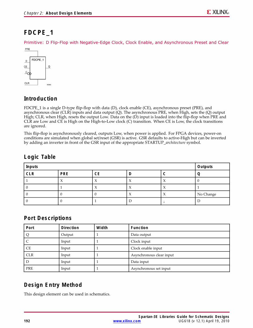
Chapter 2: About Design Elements
FDCPE_1Primitive: D Flip-Flop with Negative-Edge Clock, Clock Enable, and Asynchronous Preset and Clear
IntroductionFDCPE_1 is a single D-type flip-flop with data (D), clock enable (CE), asynchronous preset (PRE), andasynchronous clear (CLR) inputs and data output (Q). The asynchronous PRE, when High, sets the (Q) outputHigh; CLR, when High, resets the output Low. Data on the (D) input is loaded into the flip-flop when PRE andCLR are Low and CE is High on the High-to-Low clock (C) transition. When CE is Low, the clock transitionsare ignored.
This flip-flop is asynchronously cleared, outputs Low, when power is applied. For FPGA devices, power-onconditions are simulated when global set/reset (GSR) is active. GSR defaults to active-High but can be invertedby adding an inverter in front of the GSR input of the appropriate STARTUP_architecture symbol.
Logic TableInputs Outputs
CLR PRE CE D C Q1 X X X X 0
0 1 X X X 1
0 0 0 X X No Change
0 0 1 D ↓ D
Port DescriptionsPort Direction Width FunctionQ Output 1 Data output
C Input 1 Clock input
CE Input 1 Clock enable input
CLR Input 1 Asynchronous clear input
D Input 1 Data input
PRE Input 1 Asynchronous set input
Design Entry MethodThis design element can be used in schematics.
Spartan-3E Libraries Guide for Schematic Designs192 www.xilinx.com UG618 (v 12.1) April 19, 2010
Chapter 2: About Design Elements
Available AttributesAttribute Type Allowed Values Default DescriptionINIT Binary 0,1 0 Sets the initial value of Q output after
configuration.
For More Information• See the Spartan-3 Generation FPGA User Guide.
• See the Spartan-3E FPGA Family Complete Data Sheet.
Spartan-3E Libraries Guide for Schematic DesignsUG618 (v 12.1) April 19, 2010 www.xilinx.com 193
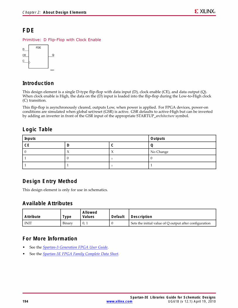
Chapter 2: About Design Elements
FDEPrimitive: D Flip-Flop with Clock Enable
IntroductionThis design element is a single D-type flip-flop with data input (D), clock enable (CE), and data output (Q).When clock enable is High, the data on the (D) input is loaded into the flip-flop during the Low-to-High clock(C) transition.
This flip-flop is asynchronously cleared, outputs Low, when power is applied. For FPGA devices, power-onconditions are simulated when global set/reset (GSR) is active. GSR defaults to active-High but can be invertedby adding an inverter in front of the GSR input of the appropriate STARTUP_architecture symbol.
Logic TableInputs Outputs
CE D C Q0 X X No Change
1 0 ↑ 0
1 1 ↑ 1
Design Entry MethodThis design element is only for use in schematics.
Available Attributes
Attribute TypeAllowedValues Default Description
INIT Binary 0, 1 0 Sets the initial value of Q output after configuration
For More Information• See the Spartan-3 Generation FPGA User Guide.
• See the Spartan-3E FPGA Family Complete Data Sheet.
Spartan-3E Libraries Guide for Schematic Designs194 www.xilinx.com UG618 (v 12.1) April 19, 2010
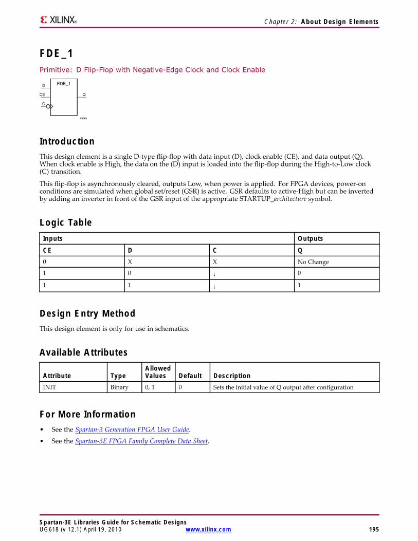
Chapter 2: About Design Elements
FDE_1Primitive: D Flip-Flop with Negative-Edge Clock and Clock Enable
IntroductionThis design element is a single D-type flip-flop with data input (D), clock enable (CE), and data output (Q).When clock enable is High, the data on the (D) input is loaded into the flip-flop during the High-to-Low clock(C) transition.
This flip-flop is asynchronously cleared, outputs Low, when power is applied. For FPGA devices, power-onconditions are simulated when global set/reset (GSR) is active. GSR defaults to active-High but can be invertedby adding an inverter in front of the GSR input of the appropriate STARTUP_architecture symbol.
Logic TableInputs Outputs
CE D C Q0 X X No Change
1 0 ↓ 0
1 1 ↓ 1
Design Entry MethodThis design element is only for use in schematics.
Available Attributes
Attribute TypeAllowedValues Default Description
INIT Binary 0, 1 0 Sets the initial value of Q output after configuration
For More Information• See the Spartan-3 Generation FPGA User Guide.
• See the Spartan-3E FPGA Family Complete Data Sheet.
Spartan-3E Libraries Guide for Schematic DesignsUG618 (v 12.1) April 19, 2010 www.xilinx.com 195
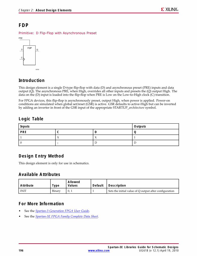
Chapter 2: About Design Elements
FDPPrimitive: D Flip-Flop with Asynchronous Preset
IntroductionThis design element is a single D-type flip-flop with data (D) and asynchronous preset (PRE) inputs and dataoutput (Q). The asynchronous PRE, when High, overrides all other inputs and presets the (Q) output High. Thedata on the (D) input is loaded into the flip-flop when PRE is Low on the Low-to-High clock (C) transition.
For FPGA devices, this flip-flop is asynchronously preset, output High, when power is applied. Power-onconditions are simulated when global set/reset (GSR) is active. GSR defaults to active-High but can be invertedby adding an inverter in front of the GSR input of the appropriate STARTUP_architecture symbol.
Logic TableInputs Outputs
PRE C D Q1 X X 1
0 ↑ D D
Design Entry MethodThis design element is only for use in schematics.
Available Attributes
Attribute TypeAllowedValues Default Description
INIT Binary 0, 1 1 Sets the initial value of Q output after configuration
For More Information• See the Spartan-3 Generation FPGA User Guide.
• See the Spartan-3E FPGA Family Complete Data Sheet.
Spartan-3E Libraries Guide for Schematic Designs196 www.xilinx.com UG618 (v 12.1) April 19, 2010
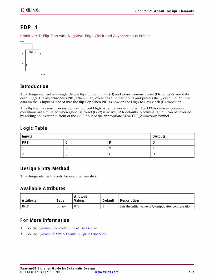
Chapter 2: About Design Elements
FDP_1Primitive: D Flip-Flop with Negative-Edge Clock and Asynchronous Preset
IntroductionThis design element is a single D-type flip-flop with data (D) and asynchronous preset (PRE) inputs and dataoutput (Q). The asynchronous PRE, when High, overrides all other inputs and presets the Q output High. Thedata on the D input is loaded into the flip-flop when PRE is Low on the High-to-Low clock (C) transition.
This flip-flop is asynchronously preset, output High, when power is applied. For FPGA devices, power-onconditions are simulated when global set/reset (GSR) is active. GSR defaults to active-High but can be invertedby adding an inverter in front of the GSR input of the appropriate STARTUP_architecture symbol.
Logic TableInputs Outputs
PRE C D Q1 X X 1
0 ↓ D D
Design Entry MethodThis design element is only for use in schematics.
Available Attributes
Attribute TypeAllowedValues Default Description
INIT Binary 0, 1 1 Sets the initial value of Q output after configuration
For More Information• See the Spartan-3 Generation FPGA User Guide.
• See the Spartan-3E FPGA Family Complete Data Sheet.
Spartan-3E Libraries Guide for Schematic DesignsUG618 (v 12.1) April 19, 2010 www.xilinx.com 197
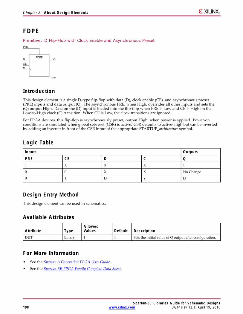
Chapter 2: About Design Elements
FDPEPrimitive: D Flip-Flop with Clock Enable and Asynchronous Preset
IntroductionThis design element is a single D-type flip-flop with data (D), clock enable (CE), and asynchronous preset(PRE) inputs and data output (Q). The asynchronous PRE, when High, overrides all other inputs and sets the(Q) output High. Data on the (D) input is loaded into the flip-flop when PRE is Low and CE is High on theLow-to-High clock (C) transition. When CE is Low, the clock transitions are ignored.
For FPGA devices, this flip-flop is asynchronously preset, output High, when power is applied. Power-onconditions are simulated when global set/reset (GSR) is active. GSR defaults to active-High but can be invertedby adding an inverter in front of the GSR input of the appropriate STARTUP_architecture symbol.
Logic TableInputs Outputs
PRE CE D C Q1 X X X 1
0 0 X X No Change
0 1 D ↑ D
Design Entry MethodThis design element can be used in schematics.
Available Attributes
Attribute TypeAllowedValues Default Description
INIT Binary 1 1 Sets the initial value of Q output after configuration.
For More Information• See the Spartan-3 Generation FPGA User Guide.
• See the Spartan-3E FPGA Family Complete Data Sheet.
Spartan-3E Libraries Guide for Schematic Designs198 www.xilinx.com UG618 (v 12.1) April 19, 2010
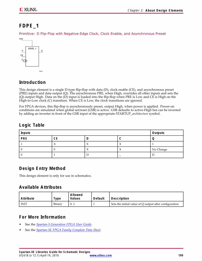
Chapter 2: About Design Elements
FDPE_1Primitive: D Flip-Flop with Negative-Edge Clock, Clock Enable, and Asynchronous Preset
IntroductionThis design element is a single D-type flip-flop with data (D), clock enable (CE), and asynchronous preset(PRE) inputs and data output (Q). The asynchronous PRE, when High, overrides all other inputs and sets the(Q) output High. Data on the (D) input is loaded into the flip-flop when PRE is Low and CE is High on theHigh-to-Low clock (C) transition. When CE is Low, the clock transitions are ignored.
For FPGA devices, this flip-flop is asynchronously preset, output High, when power is applied. Power-onconditions are simulated when global set/reset (GSR) is active. GSR defaults to active-High but can be invertedby adding an inverter in front of the GSR input of the appropriate STARTUP_architecture symbol.
Logic TableInputs Outputs
PRE CE D C Q1 X X X 1
0 0 X X No Change
0 1 D ↓ D
Design Entry MethodThis design element is only for use in schematics.
Available Attributes
Attribute TypeAllowedValues Default Description
INIT Binary 0, 1 1 Sets the initial value of Q output after configuration
For More Information• See the Spartan-3 Generation FPGA User Guide.
• See the Spartan-3E FPGA Family Complete Data Sheet.
Spartan-3E Libraries Guide for Schematic DesignsUG618 (v 12.1) April 19, 2010 www.xilinx.com 199
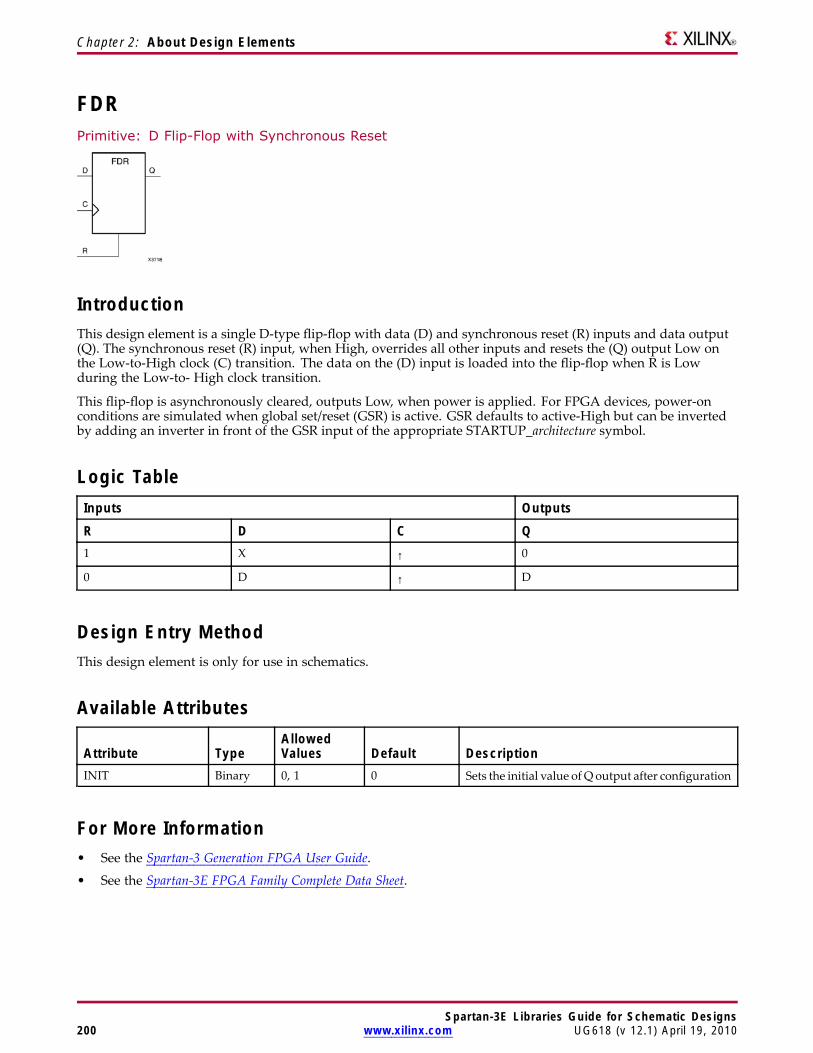
Chapter 2: About Design Elements
FDRPrimitive: D Flip-Flop with Synchronous Reset
IntroductionThis design element is a single D-type flip-flop with data (D) and synchronous reset (R) inputs and data output(Q). The synchronous reset (R) input, when High, overrides all other inputs and resets the (Q) output Low onthe Low-to-High clock (C) transition. The data on the (D) input is loaded into the flip-flop when R is Lowduring the Low-to- High clock transition.
This flip-flop is asynchronously cleared, outputs Low, when power is applied. For FPGA devices, power-onconditions are simulated when global set/reset (GSR) is active. GSR defaults to active-High but can be invertedby adding an inverter in front of the GSR input of the appropriate STARTUP_architecture symbol.
Logic TableInputs Outputs
R D C Q1 X ↑ 0
0 D ↑ D
Design Entry MethodThis design element is only for use in schematics.
Available Attributes
Attribute TypeAllowedValues Default Description
INIT Binary 0, 1 0 Sets the initial value ofQ output after configuration
For More Information• See the Spartan-3 Generation FPGA User Guide.
• See the Spartan-3E FPGA Family Complete Data Sheet.
Spartan-3E Libraries Guide for Schematic Designs200 www.xilinx.com UG618 (v 12.1) April 19, 2010
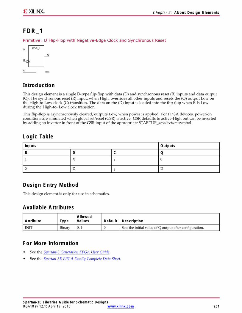
Chapter 2: About Design Elements
FDR_1Primitive: D Flip-Flop with Negative-Edge Clock and Synchronous Reset
IntroductionThis design element is a single D-type flip-flop with data (D) and synchronous reset (R) inputs and data output(Q). The synchronous reset (R) input, when High, overrides all other inputs and resets the (Q) output Low onthe High-to-Low clock (C) transition. The data on the (D) input is loaded into the flip-flop when R is Lowduring the High-to- Low clock transition.
This flip-flop is asynchronously cleared, outputs Low, when power is applied. For FPGA devices, power-onconditions are simulated when global set/reset (GSR) is active. GSR defaults to active-High but can be invertedby adding an inverter in front of the GSR input of the appropriate STARTUP_architecture symbol.
Logic TableInputs Outputs
R D C Q1 X ↓ 0
0 D ↓ D
Design Entry MethodThis design element is only for use in schematics.
Available Attributes
Attribute TypeAllowedValues Default Description
INIT Binary 0, 1 0 Sets the initial value of Q output after configuration.
For More Information• See the Spartan-3 Generation FPGA User Guide.
• See the Spartan-3E FPGA Family Complete Data Sheet.
Spartan-3E Libraries Guide for Schematic DesignsUG618 (v 12.1) April 19, 2010 www.xilinx.com 201
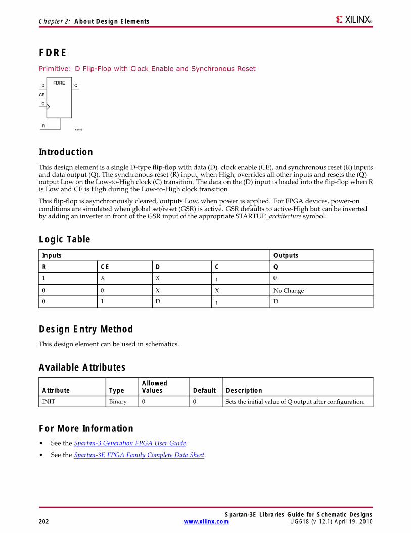
Chapter 2: About Design Elements
FDREPrimitive: D Flip-Flop with Clock Enable and Synchronous Reset
IntroductionThis design element is a single D-type flip-flop with data (D), clock enable (CE), and synchronous reset (R) inputsand data output (Q). The synchronous reset (R) input, when High, overrides all other inputs and resets the (Q)output Low on the Low-to-High clock (C) transition. The data on the (D) input is loaded into the flip-flop when Ris Low and CE is High during the Low-to-High clock transition.
This flip-flop is asynchronously cleared, outputs Low, when power is applied. For FPGA devices, power-onconditions are simulated when global set/reset (GSR) is active. GSR defaults to active-High but can be invertedby adding an inverter in front of the GSR input of the appropriate STARTUP_architecture symbol.
Logic TableInputs Outputs
R CE D C Q1 X X ↑ 0
0 0 X X No Change
0 1 D ↑ D
Design Entry MethodThis design element can be used in schematics.
Available Attributes
Attribute TypeAllowedValues Default Description
INIT Binary 0 0 Sets the initial value of Q output after configuration.
For More Information• See the Spartan-3 Generation FPGA User Guide.
• See the Spartan-3E FPGA Family Complete Data Sheet.
Spartan-3E Libraries Guide for Schematic Designs202 www.xilinx.com UG618 (v 12.1) April 19, 2010
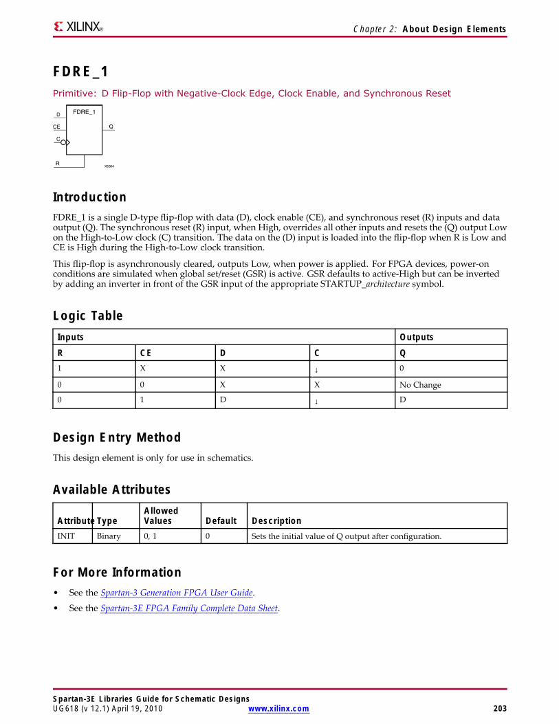
Chapter 2: About Design Elements
FDRE_1Primitive: D Flip-Flop with Negative-Clock Edge, Clock Enable, and Synchronous Reset
IntroductionFDRE_1 is a single D-type flip-flop with data (D), clock enable (CE), and synchronous reset (R) inputs and dataoutput (Q). The synchronous reset (R) input, when High, overrides all other inputs and resets the (Q) output Lowon the High-to-Low clock (C) transition. The data on the (D) input is loaded into the flip-flop when R is Low andCE is High during the High-to-Low clock transition.
This flip-flop is asynchronously cleared, outputs Low, when power is applied. For FPGA devices, power-onconditions are simulated when global set/reset (GSR) is active. GSR defaults to active-High but can be invertedby adding an inverter in front of the GSR input of the appropriate STARTUP_architecture symbol.
Logic TableInputs Outputs
R CE D C Q1 X X ↓ 0
0 0 X X No Change
0 1 D ↓ D
Design Entry MethodThis design element is only for use in schematics.
Available Attributes
Attribute TypeAllowedValues Default Description
INIT Binary 0, 1 0 Sets the initial value of Q output after configuration.
For More Information• See the Spartan-3 Generation FPGA User Guide.
• See the Spartan-3E FPGA Family Complete Data Sheet.
Spartan-3E Libraries Guide for Schematic DesignsUG618 (v 12.1) April 19, 2010 www.xilinx.com 203
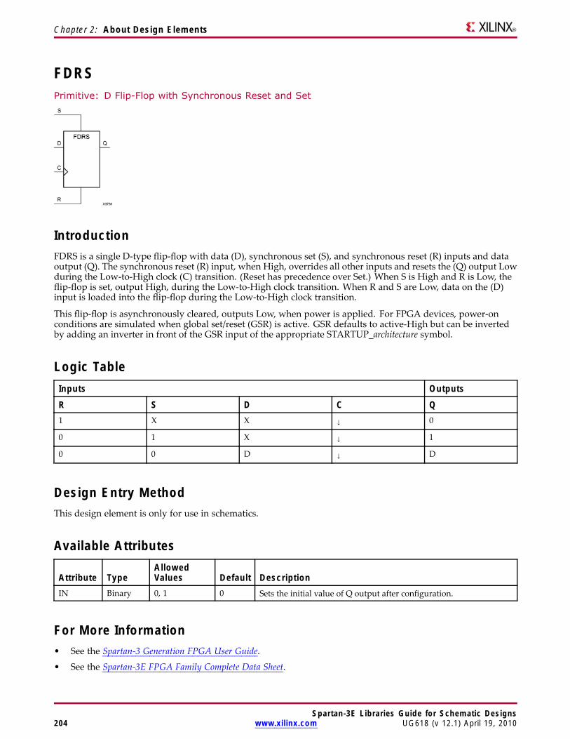
Chapter 2: About Design Elements
FDRSPrimitive: D Flip-Flop with Synchronous Reset and Set
IntroductionFDRS is a single D-type flip-flop with data (D), synchronous set (S), and synchronous reset (R) inputs and dataoutput (Q). The synchronous reset (R) input, when High, overrides all other inputs and resets the (Q) output Lowduring the Low-to-High clock (C) transition. (Reset has precedence over Set.) When S is High and R is Low, theflip-flop is set, output High, during the Low-to-High clock transition. When R and S are Low, data on the (D)input is loaded into the flip-flop during the Low-to-High clock transition.
This flip-flop is asynchronously cleared, outputs Low, when power is applied. For FPGA devices, power-onconditions are simulated when global set/reset (GSR) is active. GSR defaults to active-High but can be invertedby adding an inverter in front of the GSR input of the appropriate STARTUP_architecture symbol.
Logic TableInputs Outputs
R S D C Q1 X X ↓ 0
0 1 X ↓ 1
0 0 D ↓ D
Design Entry MethodThis design element is only for use in schematics.
Available Attributes
Attribute TypeAllowedValues Default Description
IN Binary 0, 1 0 Sets the initial value of Q output after configuration.
For More Information• See the Spartan-3 Generation FPGA User Guide.
• See the Spartan-3E FPGA Family Complete Data Sheet.
Spartan-3E Libraries Guide for Schematic Designs204 www.xilinx.com UG618 (v 12.1) April 19, 2010
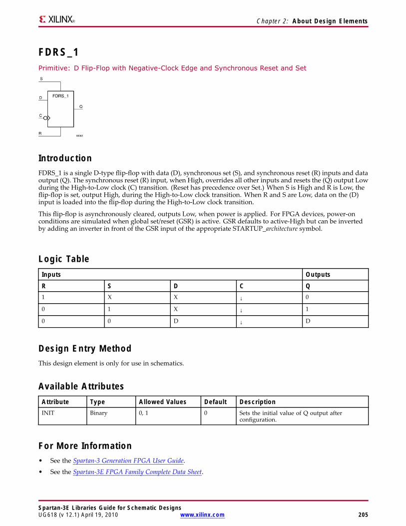
Chapter 2: About Design Elements
FDRS_1Primitive: D Flip-Flop with Negative-Clock Edge and Synchronous Reset and Set
IntroductionFDRS_1 is a single D-type flip-flop with data (D), synchronous set (S), and synchronous reset (R) inputs and dataoutput (Q). The synchronous reset (R) input, when High, overrides all other inputs and resets the (Q) output Lowduring the High-to-Low clock (C) transition. (Reset has precedence over Set.) When S is High and R is Low, theflip-flop is set, output High, during the High-to-Low clock transition. When R and S are Low, data on the (D)input is loaded into the flip-flop during the High-to-Low clock transition.
This flip-flop is asynchronously cleared, outputs Low, when power is applied. For FPGA devices, power-onconditions are simulated when global set/reset (GSR) is active. GSR defaults to active-High but can be invertedby adding an inverter in front of the GSR input of the appropriate STARTUP_architecture symbol.
Logic TableInputs Outputs
R S D C Q1 X X ↓ 0
0 1 X ↓ 1
0 0 D ↓ D
Design Entry MethodThis design element is only for use in schematics.
Available AttributesAttribute Type Allowed Values Default DescriptionINIT Binary 0, 1 0 Sets the initial value of Q output after
configuration.
For More Information• See the Spartan-3 Generation FPGA User Guide.
• See the Spartan-3E FPGA Family Complete Data Sheet.
Spartan-3E Libraries Guide for Schematic DesignsUG618 (v 12.1) April 19, 2010 www.xilinx.com 205
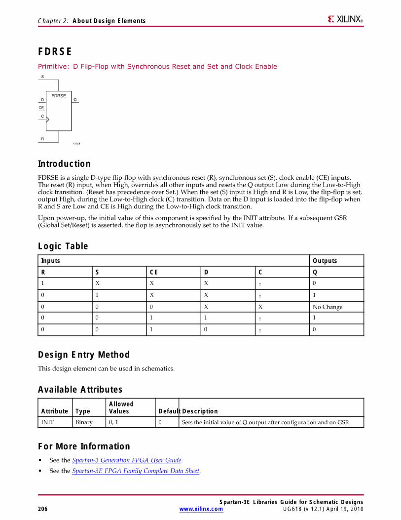
Chapter 2: About Design Elements
FDRSEPrimitive: D Flip-Flop with Synchronous Reset and Set and Clock Enable
IntroductionFDRSE is a single D-type flip-flop with synchronous reset (R), synchronous set (S), clock enable (CE) inputs.The reset (R) input, when High, overrides all other inputs and resets the Q output Low during the Low-to-Highclock transition. (Reset has precedence over Set.) When the set (S) input is High and R is Low, the flip-flop is set,output High, during the Low-to-High clock (C) transition. Data on the D input is loaded into the flip-flop whenR and S are Low and CE is High during the Low-to-High clock transition.
Upon power-up, the initial value of this component is specified by the INIT attribute. If a subsequent GSR(Global Set/Reset) is asserted, the flop is asynchronously set to the INIT value.
Logic TableInputs Outputs
R S CE D C Q1 X X X ↑ 0
0 1 X X ↑ 1
0 0 0 X X No Change
0 0 1 1 ↑ 1
0 0 1 0 ↑ 0
Design Entry MethodThis design element can be used in schematics.
Available Attributes
Attribute TypeAllowedValues Default Description
INIT Binary 0, 1 0 Sets the initial value of Q output after configuration and on GSR.
For More Information• See the Spartan-3 Generation FPGA User Guide.• See the Spartan-3E FPGA Family Complete Data Sheet.
Spartan-3E Libraries Guide for Schematic Designs206 www.xilinx.com UG618 (v 12.1) April 19, 2010
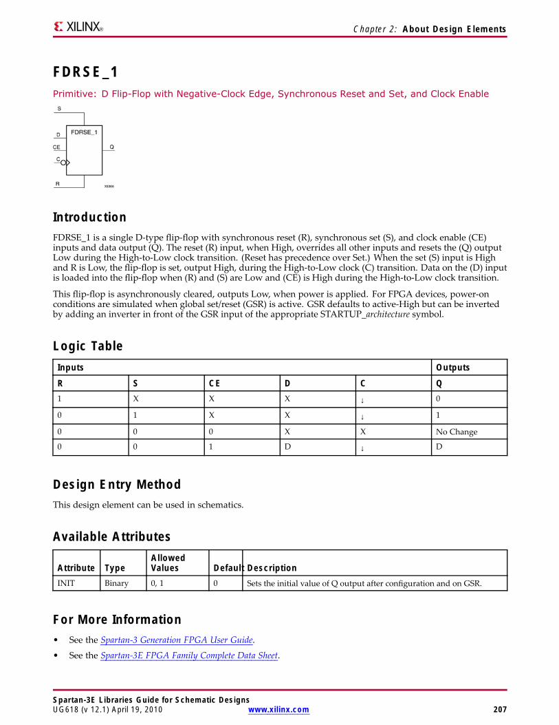
Chapter 2: About Design Elements
FDRSE_1Primitive: D Flip-Flop with Negative-Clock Edge, Synchronous Reset and Set, and Clock Enable
IntroductionFDRSE_1 is a single D-type flip-flop with synchronous reset (R), synchronous set (S), and clock enable (CE)inputs and data output (Q). The reset (R) input, when High, overrides all other inputs and resets the (Q) outputLow during the High-to-Low clock transition. (Reset has precedence over Set.) When the set (S) input is Highand R is Low, the flip-flop is set, output High, during the High-to-Low clock (C) transition. Data on the (D) inputis loaded into the flip-flop when (R) and (S) are Low and (CE) is High during the High-to-Low clock transition.
This flip-flop is asynchronously cleared, outputs Low, when power is applied. For FPGA devices, power-onconditions are simulated when global set/reset (GSR) is active. GSR defaults to active-High but can be invertedby adding an inverter in front of the GSR input of the appropriate STARTUP_architecture symbol.
Logic TableInputs Outputs
R S CE D C Q1 X X X ↓ 0
0 1 X X ↓ 1
0 0 0 X X No Change
0 0 1 D ↓ D
Design Entry MethodThis design element can be used in schematics.
Available Attributes
Attribute TypeAllowedValues Default Description
INIT Binary 0, 1 0 Sets the initial value of Q output after configuration and on GSR.
For More Information• See the Spartan-3 Generation FPGA User Guide.
• See the Spartan-3E FPGA Family Complete Data Sheet.
Spartan-3E Libraries Guide for Schematic DesignsUG618 (v 12.1) April 19, 2010 www.xilinx.com 207
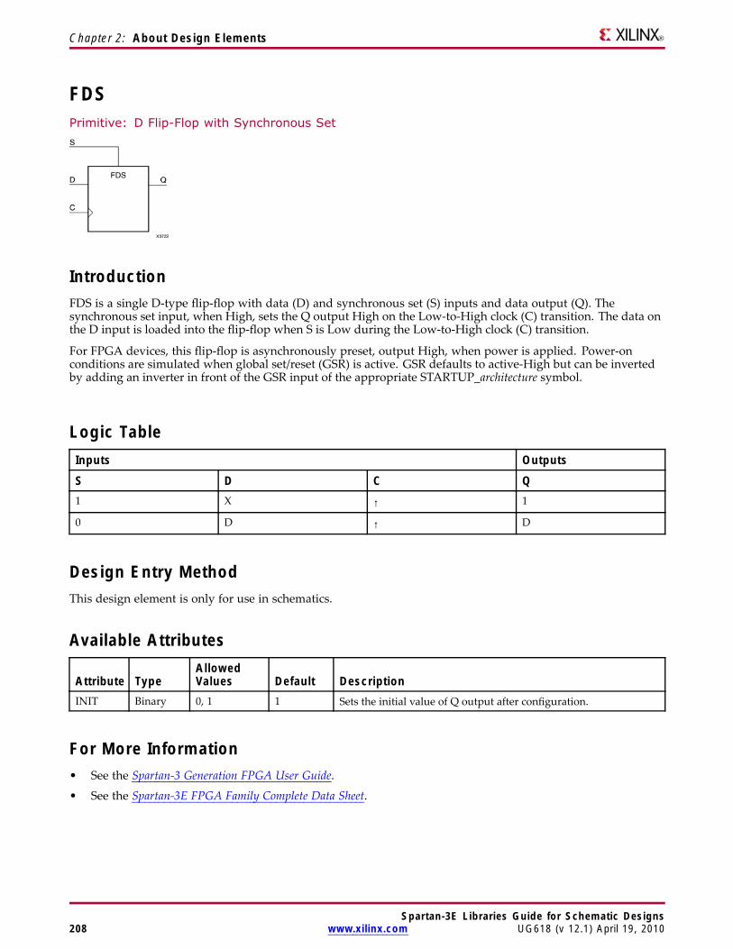
Chapter 2: About Design Elements
FDSPrimitive: D Flip-Flop with Synchronous Set
IntroductionFDS is a single D-type flip-flop with data (D) and synchronous set (S) inputs and data output (Q). Thesynchronous set input, when High, sets the Q output High on the Low-to-High clock (C) transition. The data onthe D input is loaded into the flip-flop when S is Low during the Low-to-High clock (C) transition.
For FPGA devices, this flip-flop is asynchronously preset, output High, when power is applied. Power-onconditions are simulated when global set/reset (GSR) is active. GSR defaults to active-High but can be invertedby adding an inverter in front of the GSR input of the appropriate STARTUP_architecture symbol.
Logic TableInputs Outputs
S D C Q1 X ↑ 1
0 D ↑ D
Design Entry MethodThis design element is only for use in schematics.
Available Attributes
Attribute TypeAllowedValues Default Description
INIT Binary 0, 1 1 Sets the initial value of Q output after configuration.
For More Information• See the Spartan-3 Generation FPGA User Guide.
• See the Spartan-3E FPGA Family Complete Data Sheet.
Spartan-3E Libraries Guide for Schematic Designs208 www.xilinx.com UG618 (v 12.1) April 19, 2010
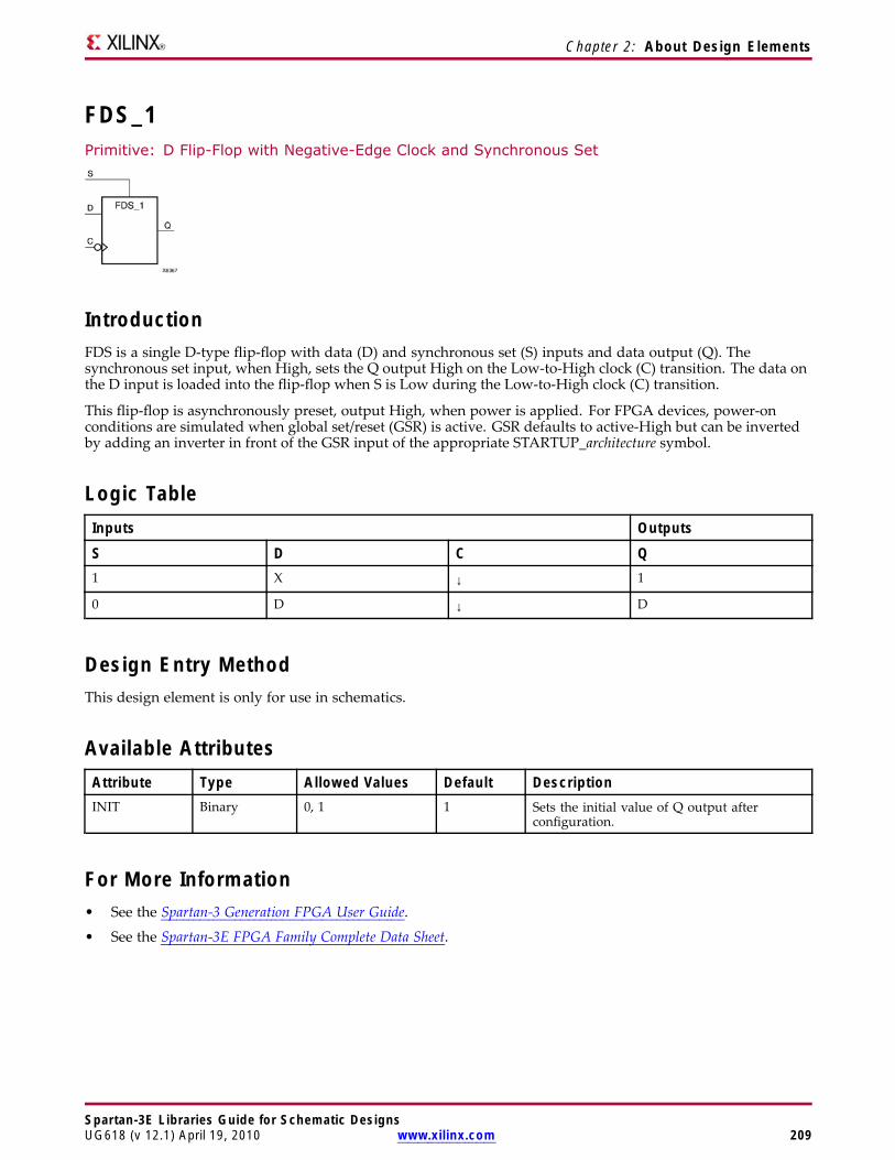
Chapter 2: About Design Elements
FDS_1Primitive: D Flip-Flop with Negative-Edge Clock and Synchronous Set
IntroductionFDS is a single D-type flip-flop with data (D) and synchronous set (S) inputs and data output (Q). Thesynchronous set input, when High, sets the Q output High on the Low-to-High clock (C) transition. The data onthe D input is loaded into the flip-flop when S is Low during the Low-to-High clock (C) transition.
This flip-flop is asynchronously preset, output High, when power is applied. For FPGA devices, power-onconditions are simulated when global set/reset (GSR) is active. GSR defaults to active-High but can be invertedby adding an inverter in front of the GSR input of the appropriate STARTUP_architecture symbol.
Logic TableInputs Outputs
S D C Q1 X ↓ 1
0 D ↓ D
Design Entry MethodThis design element is only for use in schematics.
Available AttributesAttribute Type Allowed Values Default DescriptionINIT Binary 0, 1 1 Sets the initial value of Q output after
configuration.
For More Information• See the Spartan-3 Generation FPGA User Guide.
• See the Spartan-3E FPGA Family Complete Data Sheet.
Spartan-3E Libraries Guide for Schematic DesignsUG618 (v 12.1) April 19, 2010 www.xilinx.com 209
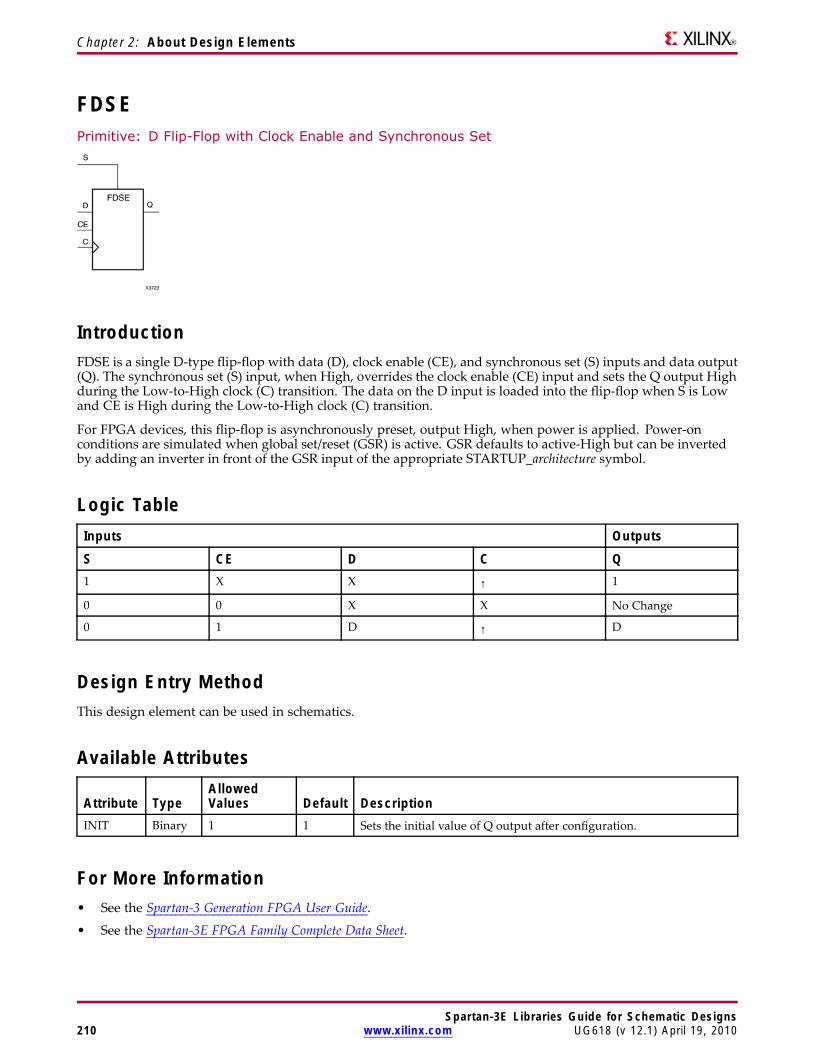
Chapter 2: About Design Elements
FDSEPrimitive: D Flip-Flop with Clock Enable and Synchronous Set
IntroductionFDSE is a single D-type flip-flop with data (D), clock enable (CE), and synchronous set (S) inputs and data output(Q). The synchronous set (S) input, when High, overrides the clock enable (CE) input and sets the Q output Highduring the Low-to-High clock (C) transition. The data on the D input is loaded into the flip-flop when S is Lowand CE is High during the Low-to-High clock (C) transition.
For FPGA devices, this flip-flop is asynchronously preset, output High, when power is applied. Power-onconditions are simulated when global set/reset (GSR) is active. GSR defaults to active-High but can be invertedby adding an inverter in front of the GSR input of the appropriate STARTUP_architecture symbol.
Logic TableInputs Outputs
S CE D C Q1 X X ↑ 1
0 0 X X No Change
0 1 D ↑ D
Design Entry MethodThis design element can be used in schematics.
Available Attributes
Attribute TypeAllowedValues Default Description
INIT Binary 1 1 Sets the initial value of Q output after configuration.
For More Information• See the Spartan-3 Generation FPGA User Guide.
• See the Spartan-3E FPGA Family Complete Data Sheet.
Spartan-3E Libraries Guide for Schematic Designs210 www.xilinx.com UG618 (v 12.1) April 19, 2010
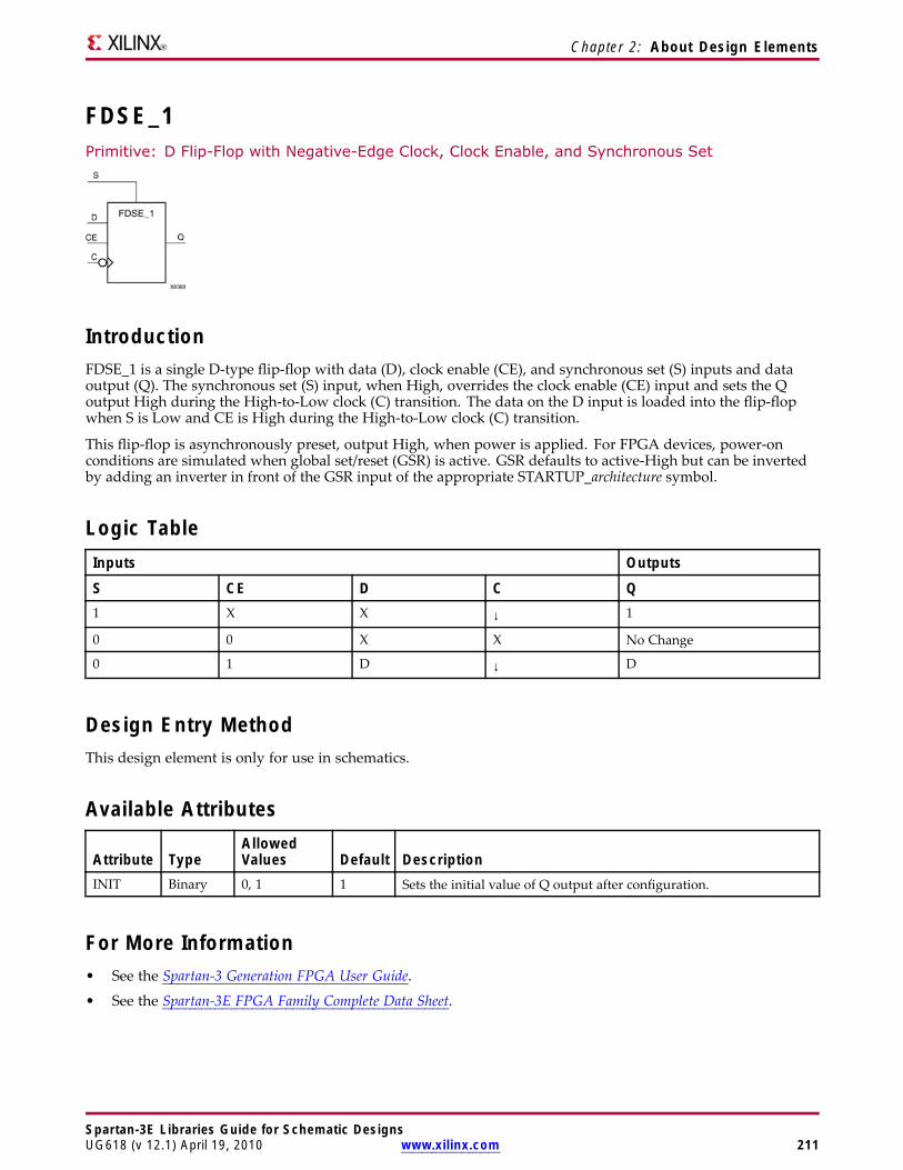
Chapter 2: About Design Elements
FDSE_1Primitive: D Flip-Flop with Negative-Edge Clock, Clock Enable, and Synchronous Set
IntroductionFDSE_1 is a single D-type flip-flop with data (D), clock enable (CE), and synchronous set (S) inputs and dataoutput (Q). The synchronous set (S) input, when High, overrides the clock enable (CE) input and sets the Qoutput High during the High-to-Low clock (C) transition. The data on the D input is loaded into the flip-flopwhen S is Low and CE is High during the High-to-Low clock (C) transition.
This flip-flop is asynchronously preset, output High, when power is applied. For FPGA devices, power-onconditions are simulated when global set/reset (GSR) is active. GSR defaults to active-High but can be invertedby adding an inverter in front of the GSR input of the appropriate STARTUP_architecture symbol.
Logic TableInputs Outputs
S CE D C Q1 X X ↓ 1
0 0 X X No Change
0 1 D ↓ D
Design Entry MethodThis design element is only for use in schematics.
Available Attributes
Attribute TypeAllowedValues Default Description
INIT Binary 0, 1 1 Sets the initial value of Q output after configuration.
For More Information• See the Spartan-3 Generation FPGA User Guide.
• See the Spartan-3E FPGA Family Complete Data Sheet.
Spartan-3E Libraries Guide for Schematic DesignsUG618 (v 12.1) April 19, 2010 www.xilinx.com 211
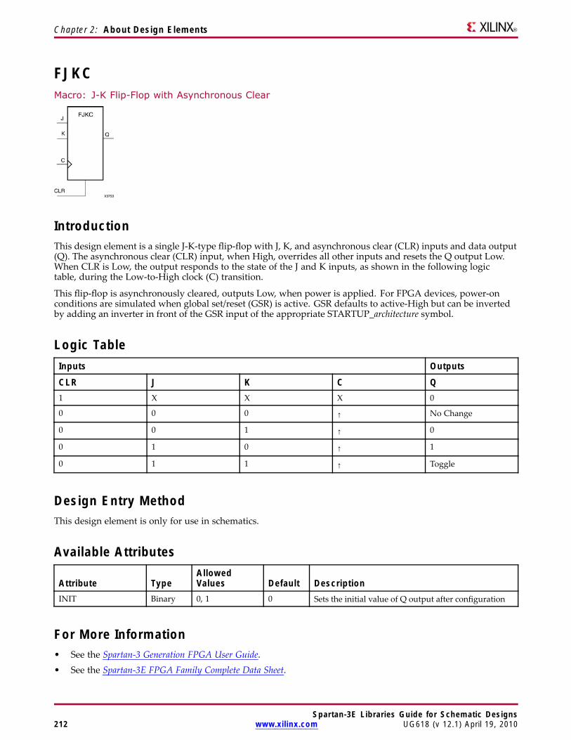
Chapter 2: About Design Elements
FJKCMacro: J-K Flip-Flop with Asynchronous Clear
IntroductionThis design element is a single J-K-type flip-flop with J, K, and asynchronous clear (CLR) inputs and data output(Q). The asynchronous clear (CLR) input, when High, overrides all other inputs and resets the Q output Low.When CLR is Low, the output responds to the state of the J and K inputs, as shown in the following logictable, during the Low-to-High clock (C) transition.
This flip-flop is asynchronously cleared, outputs Low, when power is applied. For FPGA devices, power-onconditions are simulated when global set/reset (GSR) is active. GSR defaults to active-High but can be invertedby adding an inverter in front of the GSR input of the appropriate STARTUP_architecture symbol.
Logic TableInputs Outputs
CLR J K C Q1 X X X 0
0 0 0 ↑ No Change
0 0 1 ↑ 0
0 1 0 ↑ 1
0 1 1 ↑ Toggle
Design Entry MethodThis design element is only for use in schematics.
Available Attributes
Attribute TypeAllowedValues Default Description
INIT Binary 0, 1 0 Sets the initial value of Q output after configuration
For More Information• See the Spartan-3 Generation FPGA User Guide.• See the Spartan-3E FPGA Family Complete Data Sheet.
Spartan-3E Libraries Guide for Schematic Designs212 www.xilinx.com UG618 (v 12.1) April 19, 2010
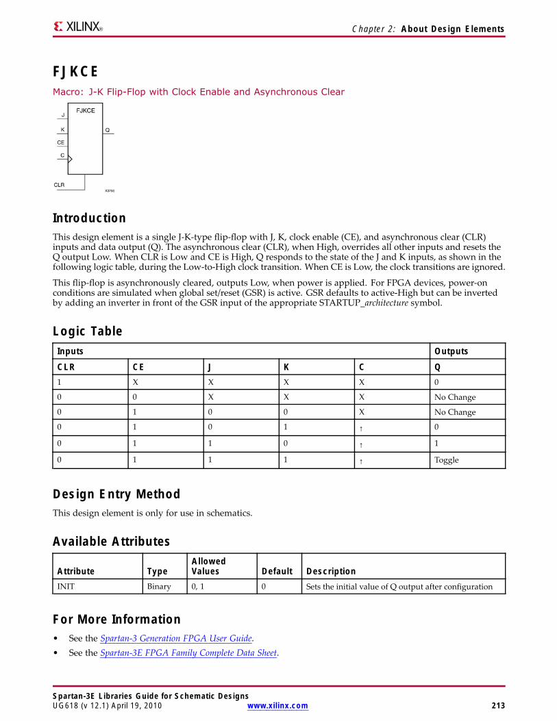
Chapter 2: About Design Elements
FJKCEMacro: J-K Flip-Flop with Clock Enable and Asynchronous Clear
IntroductionThis design element is a single J-K-type flip-flop with J, K, clock enable (CE), and asynchronous clear (CLR)inputs and data output (Q). The asynchronous clear (CLR), when High, overrides all other inputs and resets theQ output Low. When CLR is Low and CE is High, Q responds to the state of the J and K inputs, as shown in thefollowing logic table, during the Low-to-High clock transition. When CE is Low, the clock transitions are ignored.
This flip-flop is asynchronously cleared, outputs Low, when power is applied. For FPGA devices, power-onconditions are simulated when global set/reset (GSR) is active. GSR defaults to active-High but can be invertedby adding an inverter in front of the GSR input of the appropriate STARTUP_architecture symbol.
Logic TableInputs Outputs
CLR CE J K C Q1 X X X X 0
0 0 X X X No Change
0 1 0 0 X No Change
0 1 0 1 ↑ 0
0 1 1 0 ↑ 1
0 1 1 1 ↑ Toggle
Design Entry MethodThis design element is only for use in schematics.
Available Attributes
Attribute TypeAllowedValues Default Description
INIT Binary 0, 1 0 Sets the initial value of Q output after configuration
For More Information• See the Spartan-3 Generation FPGA User Guide.• See the Spartan-3E FPGA Family Complete Data Sheet.
Spartan-3E Libraries Guide for Schematic DesignsUG618 (v 12.1) April 19, 2010 www.xilinx.com 213
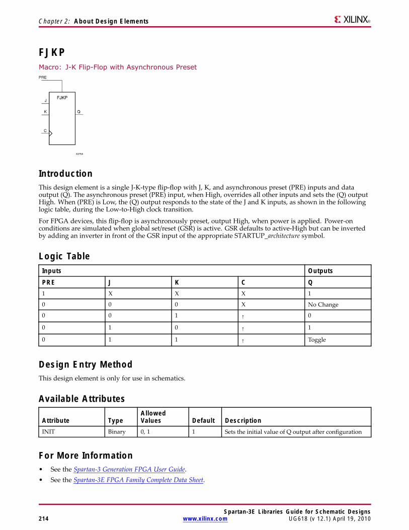
Chapter 2: About Design Elements
FJKPMacro: J-K Flip-Flop with Asynchronous Preset
IntroductionThis design element is a single J-K-type flip-flop with J, K, and asynchronous preset (PRE) inputs and dataoutput (Q). The asynchronous preset (PRE) input, when High, overrides all other inputs and sets the (Q) outputHigh. When (PRE) is Low, the (Q) output responds to the state of the J and K inputs, as shown in the followinglogic table, during the Low-to-High clock transition.
For FPGA devices, this flip-flop is asynchronously preset, output High, when power is applied. Power-onconditions are simulated when global set/reset (GSR) is active. GSR defaults to active-High but can be invertedby adding an inverter in front of the GSR input of the appropriate STARTUP_architecture symbol.
Logic TableInputs Outputs
PRE J K C Q1 X X X 1
0 0 0 X No Change
0 0 1 ↑ 0
0 1 0 ↑ 1
0 1 1 ↑ Toggle
Design Entry MethodThis design element is only for use in schematics.
Available Attributes
Attribute TypeAllowedValues Default Description
INIT Binary 0, 1 1 Sets the initial value of Q output after configuration
For More Information• See the Spartan-3 Generation FPGA User Guide.• See the Spartan-3E FPGA Family Complete Data Sheet.
Spartan-3E Libraries Guide for Schematic Designs214 www.xilinx.com UG618 (v 12.1) April 19, 2010
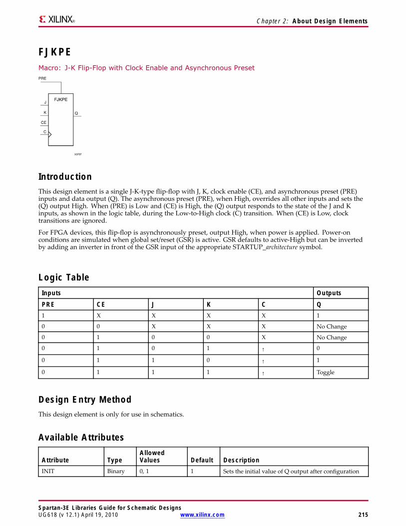
Chapter 2: About Design Elements
FJKPEMacro: J-K Flip-Flop with Clock Enable and Asynchronous Preset
IntroductionThis design element is a single J-K-type flip-flop with J, K, clock enable (CE), and asynchronous preset (PRE)inputs and data output (Q). The asynchronous preset (PRE), when High, overrides all other inputs and sets the(Q) output High. When (PRE) is Low and (CE) is High, the (Q) output responds to the state of the J and Kinputs, as shown in the logic table, during the Low-to-High clock (C) transition. When (CE) is Low, clocktransitions are ignored.
For FPGA devices, this flip-flop is asynchronously preset, output High, when power is applied. Power-onconditions are simulated when global set/reset (GSR) is active. GSR defaults to active-High but can be invertedby adding an inverter in front of the GSR input of the appropriate STARTUP_architecture symbol.
Logic TableInputs Outputs
PRE CE J K C Q1 X X X X 1
0 0 X X X No Change
0 1 0 0 X No Change
0 1 0 1 ↑ 0
0 1 1 0 ↑ 1
0 1 1 1 ↑ Toggle
Design Entry MethodThis design element is only for use in schematics.
Available Attributes
Attribute TypeAllowedValues Default Description
INIT Binary 0, 1 1 Sets the initial value of Q output after configuration
Spartan-3E Libraries Guide for Schematic DesignsUG618 (v 12.1) April 19, 2010 www.xilinx.com 215

Chapter 2: About Design Elements
For More Information• See the Spartan-3 Generation FPGA User Guide.
• See the Spartan-3E FPGA Family Complete Data Sheet.
Spartan-3E Libraries Guide for Schematic Designs216 www.xilinx.com UG618 (v 12.1) April 19, 2010
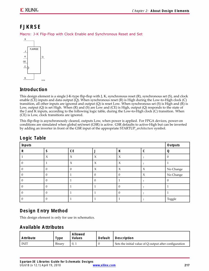
Chapter 2: About Design Elements
FJKRSEMacro: J-K Flip-Flop with Clock Enable and Synchronous Reset and Set
IntroductionThis design element is a single J-K-type flip-flop with J, K, synchronous reset (R), synchronous set (S), and clockenable (CE) inputs and data output (Q). When synchronous reset (R) is High during the Low-to-High clock (C)transition, all other inputs are ignored and output (Q) is reset Low. When synchronous set (S) is High and (R) isLow, output (Q) is set High. When (R) and (S) are Low and (CE) is High, output (Q) responds to the state ofthe J and K inputs, according to the following logic table, during the Low-to-High clock (C) transition. When(CE) is Low, clock transitions are ignored.
This flip-flop is asynchronously cleared, outputs Low, when power is applied. For FPGA devices, power-onconditions are simulated when global set/reset (GSR) is active. GSR defaults to active-High but can be invertedby adding an inverter in front of the GSR input of the appropriate STARTUP_architecture symbol.
Logic TableInputs Outputs
R S CE J K C Q1 X X X X ↑ 0
0 1 X X X ↑ 1
0 0 0 X X X No Change
0 0 1 0 0 X No Change
0 0 1 0 1 ↑ 0
0 0 1 1 0 ↑ 1
0 0 1 1 0 ↑ 1
0 0 1 1 1 ↑ Toggle
Design Entry MethodThis design element is only for use in schematics.
Available Attributes
Attribute TypeAllowedValues Default Description
INIT Binary 0, 1 0 Sets the initial value of Q output after configuration
Spartan-3E Libraries Guide for Schematic DesignsUG618 (v 12.1) April 19, 2010 www.xilinx.com 217

Chapter 2: About Design Elements
For More Information• See the Spartan-3 Generation FPGA User Guide.
• See the Spartan-3E FPGA Family Complete Data Sheet.
Spartan-3E Libraries Guide for Schematic Designs218 www.xilinx.com UG618 (v 12.1) April 19, 2010
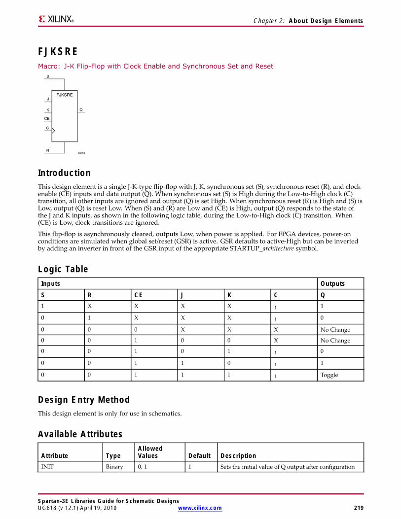
Chapter 2: About Design Elements
FJKSREMacro: J-K Flip-Flop with Clock Enable and Synchronous Set and Reset
IntroductionThis design element is a single J-K-type flip-flop with J, K, synchronous set (S), synchronous reset (R), and clockenable (CE) inputs and data output (Q). When synchronous set (S) is High during the Low-to-High clock (C)transition, all other inputs are ignored and output (Q) is set High. When synchronous reset (R) is High and (S) isLow, output (Q) is reset Low. When (S) and (R) are Low and (CE) is High, output (Q) responds to the state ofthe J and K inputs, as shown in the following logic table, during the Low-to-High clock (C) transition. When(CE) is Low, clock transitions are ignored.
This flip-flop is asynchronously cleared, outputs Low, when power is applied. For FPGA devices, power-onconditions are simulated when global set/reset (GSR) is active. GSR defaults to active-High but can be invertedby adding an inverter in front of the GSR input of the appropriate STARTUP_architecture symbol.
Logic TableInputs Outputs
S R CE J K C Q1 X X X X ↑ 1
0 1 X X X ↑ 0
0 0 0 X X X No Change
0 0 1 0 0 X No Change
0 0 1 0 1 ↑ 0
0 0 1 1 0 ↑ 1
0 0 1 1 1 ↑ Toggle
Design Entry MethodThis design element is only for use in schematics.
Available Attributes
Attribute TypeAllowedValues Default Description
INIT Binary 0, 1 1 Sets the initial value of Q output after configuration
Spartan-3E Libraries Guide for Schematic DesignsUG618 (v 12.1) April 19, 2010 www.xilinx.com 219

Chapter 2: About Design Elements
For More Information• See the Spartan-3 Generation FPGA User Guide.
• See the Spartan-3E FPGA Family Complete Data Sheet.
Spartan-3E Libraries Guide for Schematic Designs220 www.xilinx.com UG618 (v 12.1) April 19, 2010
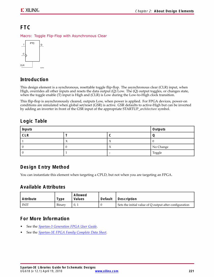
Chapter 2: About Design Elements
FTCMacro: Toggle Flip-Flop with Asynchronous Clear
IntroductionThis design element is a synchronous, resettable toggle flip-flop. The asynchronous clear (CLR) input, whenHigh, overrides all other inputs and resets the data output (Q) Low. The (Q) output toggles, or changes state,when the toggle enable (T) input is High and (CLR) is Low during the Low-to-High clock transition.
This flip-flop is asynchronously cleared, outputs Low, when power is applied. For FPGA devices, power-onconditions are simulated when global set/reset (GSR) is active. GSR defaults to active-High but can be invertedby adding an inverter in front of the GSR input of the appropriate STARTUP_architecture symbol.
Logic TableInputs Outputs
CLR T C Q1 X X 0
0 0 X No Change
0 1 ↑ Toggle
Design Entry MethodYou can instantiate this element when targeting a CPLD, but not when you are targeting an FPGA.
Available Attributes
Attribute TypeAllowedValues Default Description
INIT Binary 0, 1 0 Sets the initial value of Q output after configuration
For More Information• See the Spartan-3 Generation FPGA User Guide.
• See the Spartan-3E FPGA Family Complete Data Sheet.
Spartan-3E Libraries Guide for Schematic DesignsUG618 (v 12.1) April 19, 2010 www.xilinx.com 221
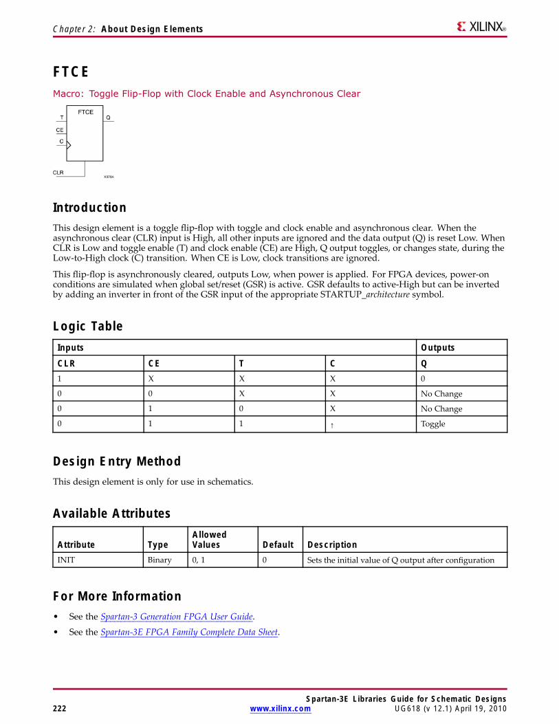
Chapter 2: About Design Elements
FTCEMacro: Toggle Flip-Flop with Clock Enable and Asynchronous Clear
IntroductionThis design element is a toggle flip-flop with toggle and clock enable and asynchronous clear. When theasynchronous clear (CLR) input is High, all other inputs are ignored and the data output (Q) is reset Low. WhenCLR is Low and toggle enable (T) and clock enable (CE) are High, Q output toggles, or changes state, during theLow-to-High clock (C) transition. When CE is Low, clock transitions are ignored.
This flip-flop is asynchronously cleared, outputs Low, when power is applied. For FPGA devices, power-onconditions are simulated when global set/reset (GSR) is active. GSR defaults to active-High but can be invertedby adding an inverter in front of the GSR input of the appropriate STARTUP_architecture symbol.
Logic TableInputs Outputs
CLR CE T C Q1 X X X 0
0 0 X X No Change
0 1 0 X No Change
0 1 1 ↑ Toggle
Design Entry MethodThis design element is only for use in schematics.
Available Attributes
Attribute TypeAllowedValues Default Description
INIT Binary 0, 1 0 Sets the initial value of Q output after configuration
For More Information• See the Spartan-3 Generation FPGA User Guide.
• See the Spartan-3E FPGA Family Complete Data Sheet.
Spartan-3E Libraries Guide for Schematic Designs222 www.xilinx.com UG618 (v 12.1) April 19, 2010
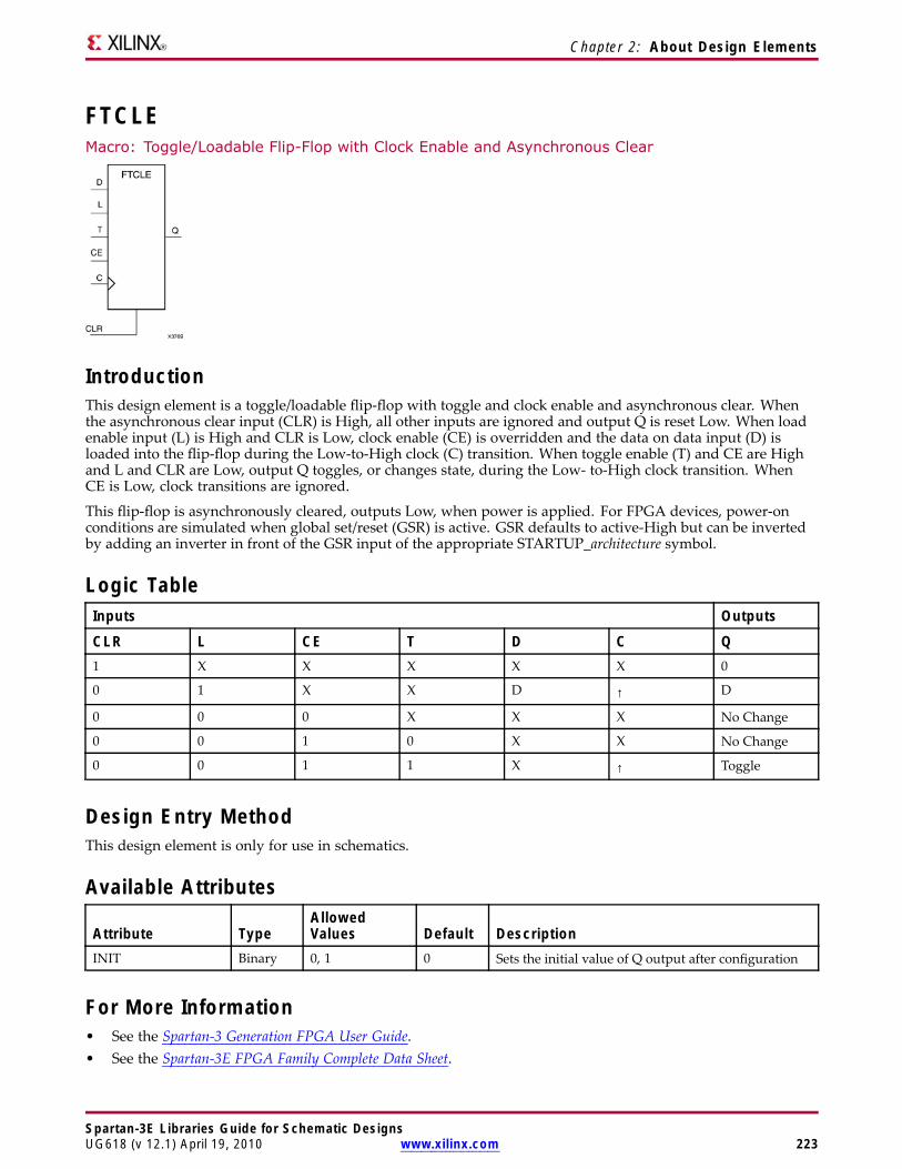
Chapter 2: About Design Elements
FTCLEMacro: Toggle/Loadable Flip-Flop with Clock Enable and Asynchronous Clear
IntroductionThis design element is a toggle/loadable flip-flop with toggle and clock enable and asynchronous clear. Whenthe asynchronous clear input (CLR) is High, all other inputs are ignored and output Q is reset Low. When loadenable input (L) is High and CLR is Low, clock enable (CE) is overridden and the data on data input (D) isloaded into the flip-flop during the Low-to-High clock (C) transition. When toggle enable (T) and CE are Highand L and CLR are Low, output Q toggles, or changes state, during the Low- to-High clock transition. WhenCE is Low, clock transitions are ignored.
This flip-flop is asynchronously cleared, outputs Low, when power is applied. For FPGA devices, power-onconditions are simulated when global set/reset (GSR) is active. GSR defaults to active-High but can be invertedby adding an inverter in front of the GSR input of the appropriate STARTUP_architecture symbol.
Logic TableInputs Outputs
CLR L CE T D C Q1 X X X X X 0
0 1 X X D ↑ D
0 0 0 X X X No Change
0 0 1 0 X X No Change
0 0 1 1 X ↑ Toggle
Design Entry MethodThis design element is only for use in schematics.
Available Attributes
Attribute TypeAllowedValues Default Description
INIT Binary 0, 1 0 Sets the initial value of Q output after configuration
For More Information• See the Spartan-3 Generation FPGA User Guide.• See the Spartan-3E FPGA Family Complete Data Sheet.
Spartan-3E Libraries Guide for Schematic DesignsUG618 (v 12.1) April 19, 2010 www.xilinx.com 223
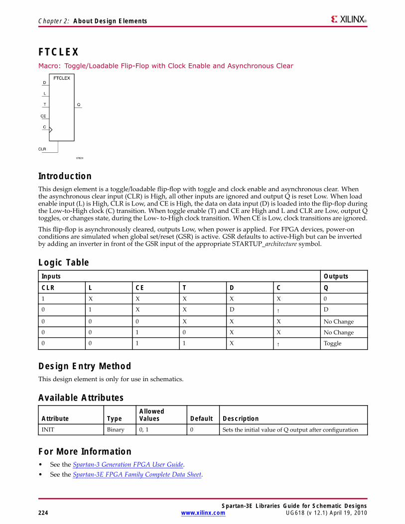
Chapter 2: About Design Elements
FTCLEXMacro: Toggle/Loadable Flip-Flop with Clock Enable and Asynchronous Clear
IntroductionThis design element is a toggle/loadable flip-flop with toggle and clock enable and asynchronous clear. Whenthe asynchronous clear input (CLR) is High, all other inputs are ignored and output Q is reset Low. When loadenable input (L) is High, CLR is Low, and CE is High, the data on data input (D) is loaded into the flip-flop duringthe Low-to-High clock (C) transition. When toggle enable (T) and CE are High and L and CLR are Low, output Qtoggles, or changes state, during the Low- to-High clock transition. When CE is Low, clock transitions are ignored.
This flip-flop is asynchronously cleared, outputs Low, when power is applied. For FPGA devices, power-onconditions are simulated when global set/reset (GSR) is active. GSR defaults to active-High but can be invertedby adding an inverter in front of the GSR input of the appropriate STARTUP_architecture symbol.
Logic TableInputs Outputs
CLR L CE T D C Q1 X X X X X 0
0 1 X X D ↑ D
0 0 0 X X X No Change
0 0 1 0 X X No Change
0 0 1 1 X ↑ Toggle
Design Entry MethodThis design element is only for use in schematics.
Available Attributes
Attribute TypeAllowedValues Default Description
INIT Binary 0, 1 0 Sets the initial value of Q output after configuration
For More Information• See the Spartan-3 Generation FPGA User Guide.• See the Spartan-3E FPGA Family Complete Data Sheet.
Spartan-3E Libraries Guide for Schematic Designs224 www.xilinx.com UG618 (v 12.1) April 19, 2010
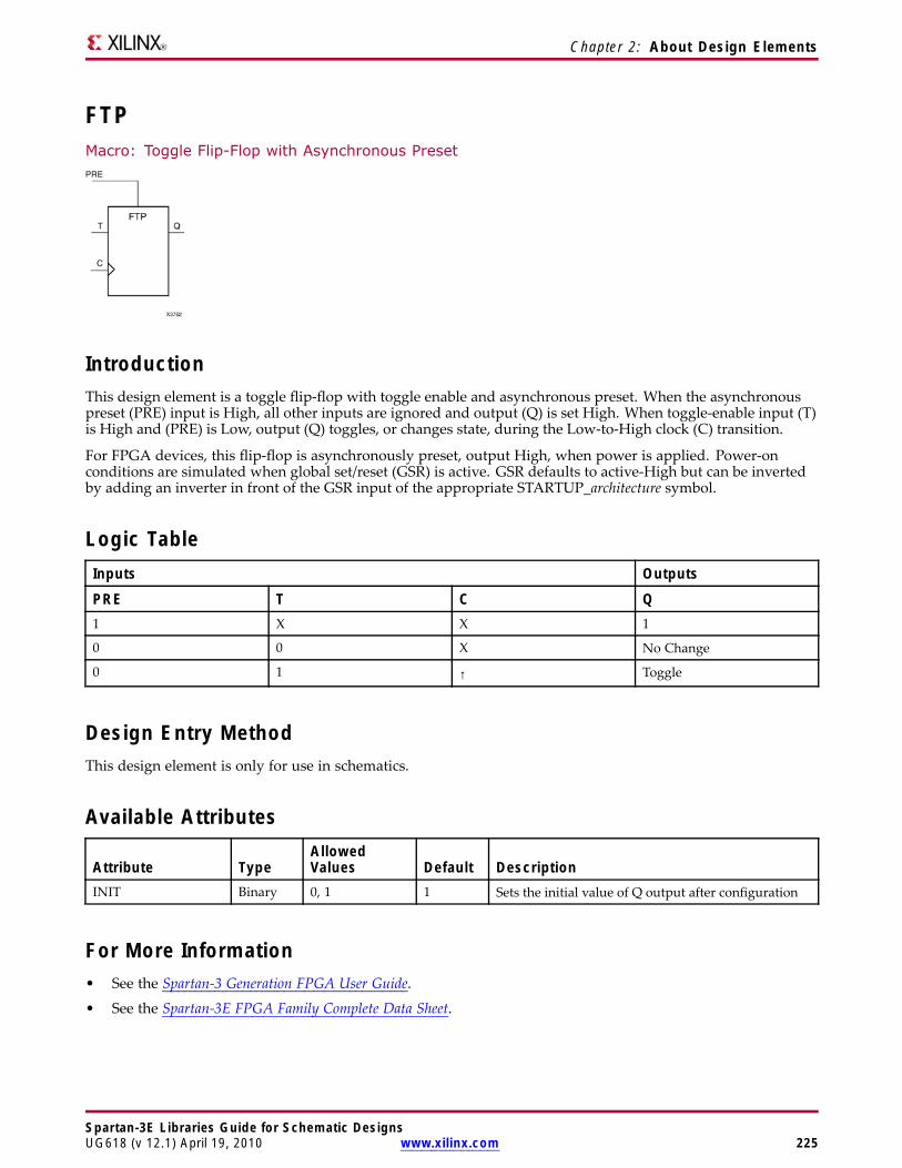
Chapter 2: About Design Elements
FTPMacro: Toggle Flip-Flop with Asynchronous Preset
IntroductionThis design element is a toggle flip-flop with toggle enable and asynchronous preset. When the asynchronouspreset (PRE) input is High, all other inputs are ignored and output (Q) is set High. When toggle-enable input (T)is High and (PRE) is Low, output (Q) toggles, or changes state, during the Low-to-High clock (C) transition.
For FPGA devices, this flip-flop is asynchronously preset, output High, when power is applied. Power-onconditions are simulated when global set/reset (GSR) is active. GSR defaults to active-High but can be invertedby adding an inverter in front of the GSR input of the appropriate STARTUP_architecture symbol.
Logic TableInputs Outputs
PRE T C Q1 X X 1
0 0 X No Change
0 1 ↑ Toggle
Design Entry MethodThis design element is only for use in schematics.
Available Attributes
Attribute TypeAllowedValues Default Description
INIT Binary 0, 1 1 Sets the initial value of Q output after configuration
For More Information• See the Spartan-3 Generation FPGA User Guide.
• See the Spartan-3E FPGA Family Complete Data Sheet.
Spartan-3E Libraries Guide for Schematic DesignsUG618 (v 12.1) April 19, 2010 www.xilinx.com 225
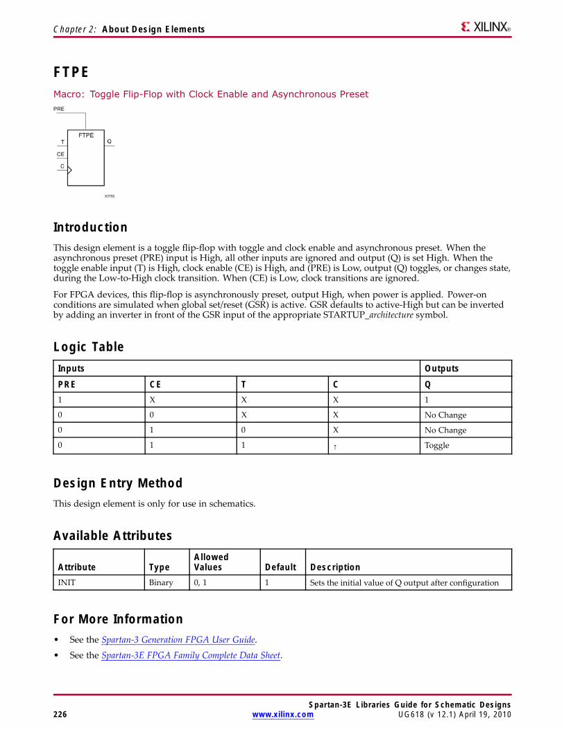
Chapter 2: About Design Elements
FTPEMacro: Toggle Flip-Flop with Clock Enable and Asynchronous Preset
IntroductionThis design element is a toggle flip-flop with toggle and clock enable and asynchronous preset. When theasynchronous preset (PRE) input is High, all other inputs are ignored and output (Q) is set High. When thetoggle enable input (T) is High, clock enable (CE) is High, and (PRE) is Low, output (Q) toggles, or changes state,during the Low-to-High clock transition. When (CE) is Low, clock transitions are ignored.
For FPGA devices, this flip-flop is asynchronously preset, output High, when power is applied. Power-onconditions are simulated when global set/reset (GSR) is active. GSR defaults to active-High but can be invertedby adding an inverter in front of the GSR input of the appropriate STARTUP_architecture symbol.
Logic TableInputs Outputs
PRE CE T C Q1 X X X 1
0 0 X X No Change
0 1 0 X No Change
0 1 1 ↑ Toggle
Design Entry MethodThis design element is only for use in schematics.
Available Attributes
Attribute TypeAllowedValues Default Description
INIT Binary 0, 1 1 Sets the initial value of Q output after configuration
For More Information• See the Spartan-3 Generation FPGA User Guide.
• See the Spartan-3E FPGA Family Complete Data Sheet.
Spartan-3E Libraries Guide for Schematic Designs226 www.xilinx.com UG618 (v 12.1) April 19, 2010
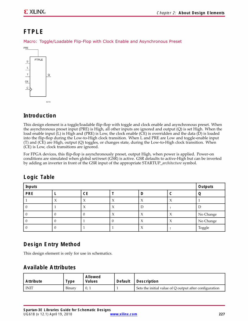
Chapter 2: About Design Elements
FTPLEMacro: Toggle/Loadable Flip-Flop with Clock Enable and Asynchronous Preset
IntroductionThis design element is a toggle/loadable flip-flop with toggle and clock enable and asynchronous preset. Whenthe asynchronous preset input (PRE) is High, all other inputs are ignored and output (Q) is set High. When theload enable input (L) is High and (PRE) is Low, the clock enable (CE) is overridden and the data (D) is loadedinto the flip-flop during the Low-to-High clock transition. When L and PRE are Low and toggle-enable input(T) and (CE) are High, output (Q) toggles, or changes state, during the Low-to-High clock transition. When(CE) is Low, clock transitions are ignored.
For FPGA devices, this flip-flop is asynchronously preset, output High, when power is applied. Power-onconditions are simulated when global set/reset (GSR) is active. GSR defaults to active-High but can be invertedby adding an inverter in front of the GSR input of the appropriate STARTUP_architecture symbol.
Logic TableInputs Outputs
PRE L CE T D C Q1 X X X X X 1
0 1 X X D ↑ D
0 0 0 X X X No Change
0 0 1 0 X X No Change
0 0 1 1 X ↑ Toggle
Design Entry MethodThis design element is only for use in schematics.
Available Attributes
Attribute TypeAllowedValues Default Description
INIT Binary 0, 1 1 Sets the initial value of Q output after configuration
Spartan-3E Libraries Guide for Schematic DesignsUG618 (v 12.1) April 19, 2010 www.xilinx.com 227

Chapter 2: About Design Elements
For More Information• See the Spartan-3 Generation FPGA User Guide.
• See the Spartan-3E FPGA Family Complete Data Sheet.
Spartan-3E Libraries Guide for Schematic Designs228 www.xilinx.com UG618 (v 12.1) April 19, 2010
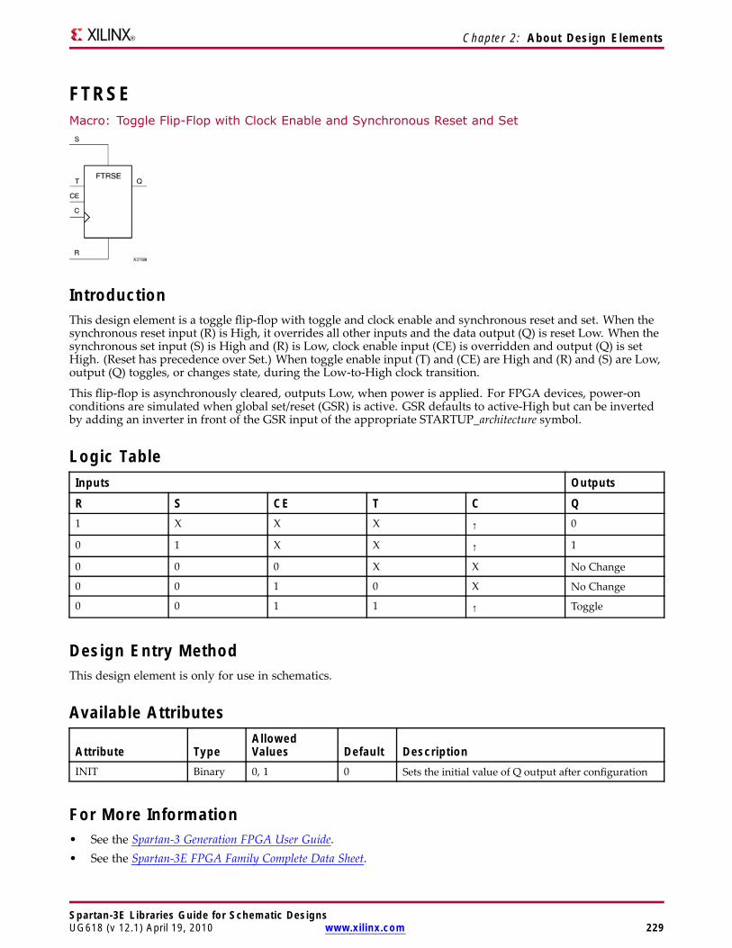
Chapter 2: About Design Elements
FTRSEMacro: Toggle Flip-Flop with Clock Enable and Synchronous Reset and Set
IntroductionThis design element is a toggle flip-flop with toggle and clock enable and synchronous reset and set. When thesynchronous reset input (R) is High, it overrides all other inputs and the data output (Q) is reset Low. When thesynchronous set input (S) is High and (R) is Low, clock enable input (CE) is overridden and output (Q) is setHigh. (Reset has precedence over Set.) When toggle enable input (T) and (CE) are High and (R) and (S) are Low,output (Q) toggles, or changes state, during the Low-to-High clock transition.
This flip-flop is asynchronously cleared, outputs Low, when power is applied. For FPGA devices, power-onconditions are simulated when global set/reset (GSR) is active. GSR defaults to active-High but can be invertedby adding an inverter in front of the GSR input of the appropriate STARTUP_architecture symbol.
Logic TableInputs Outputs
R S CE T C Q1 X X X ↑ 0
0 1 X X ↑ 1
0 0 0 X X No Change
0 0 1 0 X No Change
0 0 1 1 ↑ Toggle
Design Entry MethodThis design element is only for use in schematics.
Available Attributes
Attribute TypeAllowedValues Default Description
INIT Binary 0, 1 0 Sets the initial value of Q output after configuration
For More Information• See the Spartan-3 Generation FPGA User Guide.• See the Spartan-3E FPGA Family Complete Data Sheet.
Spartan-3E Libraries Guide for Schematic DesignsUG618 (v 12.1) April 19, 2010 www.xilinx.com 229
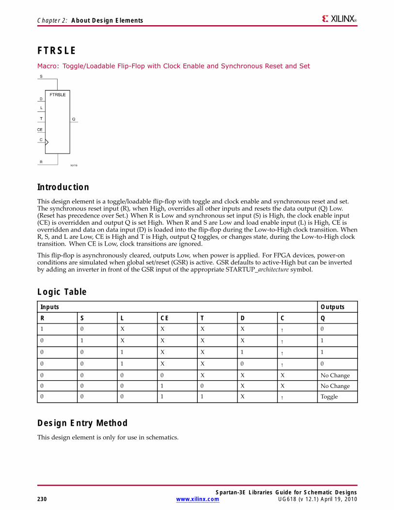
Chapter 2: About Design Elements
FTRSLEMacro: Toggle/Loadable Flip-Flop with Clock Enable and Synchronous Reset and Set
IntroductionThis design element is a toggle/loadable flip-flop with toggle and clock enable and synchronous reset and set.The synchronous reset input (R), when High, overrides all other inputs and resets the data output (Q) Low.(Reset has precedence over Set.) When R is Low and synchronous set input (S) is High, the clock enable input(CE) is overridden and output Q is set High. When R and S are Low and load enable input (L) is High, CE isoverridden and data on data input (D) is loaded into the flip-flop during the Low-to-High clock transition. WhenR, S, and L are Low, CE is High and T is High, output Q toggles, or changes state, during the Low-to-High clocktransition. When CE is Low, clock transitions are ignored.
This flip-flop is asynchronously cleared, outputs Low, when power is applied. For FPGA devices, power-onconditions are simulated when global set/reset (GSR) is active. GSR defaults to active-High but can be invertedby adding an inverter in front of the GSR input of the appropriate STARTUP_architecture symbol.
Logic TableInputs Outputs
R S L CE T D C Q1 0 X X X X ↑ 0
0 1 X X X X ↑ 1
0 0 1 X X 1 ↑ 1
0 0 1 X X 0 ↑ 0
0 0 0 0 X X X No Change
0 0 0 1 0 X X No Change
0 0 0 1 1 X ↑ Toggle
Design Entry MethodThis design element is only for use in schematics.
Spartan-3E Libraries Guide for Schematic Designs230 www.xilinx.com UG618 (v 12.1) April 19, 2010
Chapter 2: About Design Elements
Available Attributes
Attribute TypeAllowedValues Default Description
INIT Binary 0, 1 0 Sets the initial value of Q output after configuration
For More Information• See the Spartan-3 Generation FPGA User Guide.
• See the Spartan-3E FPGA Family Complete Data Sheet.
Spartan-3E Libraries Guide for Schematic DesignsUG618 (v 12.1) April 19, 2010 www.xilinx.com 231
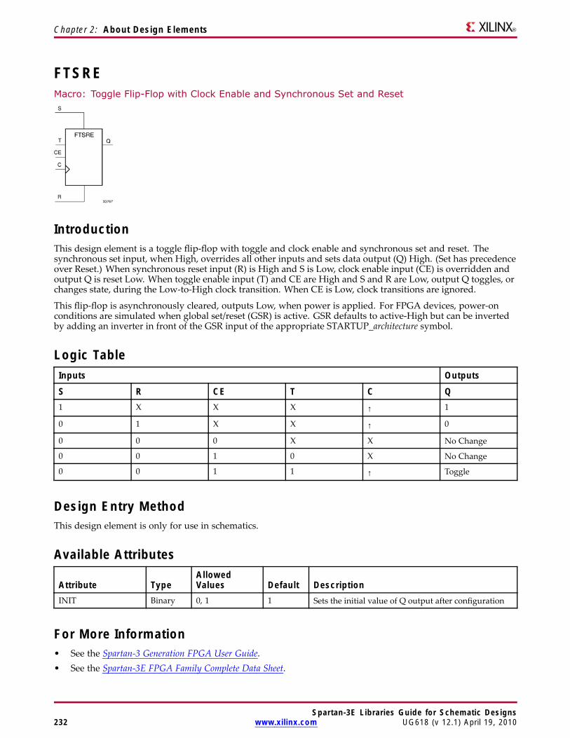
Chapter 2: About Design Elements
FTSREMacro: Toggle Flip-Flop with Clock Enable and Synchronous Set and Reset
IntroductionThis design element is a toggle flip-flop with toggle and clock enable and synchronous set and reset. Thesynchronous set input, when High, overrides all other inputs and sets data output (Q) High. (Set has precedenceover Reset.) When synchronous reset input (R) is High and S is Low, clock enable input (CE) is overridden andoutput Q is reset Low. When toggle enable input (T) and CE are High and S and R are Low, output Q toggles, orchanges state, during the Low-to-High clock transition. When CE is Low, clock transitions are ignored.
This flip-flop is asynchronously cleared, outputs Low, when power is applied. For FPGA devices, power-onconditions are simulated when global set/reset (GSR) is active. GSR defaults to active-High but can be invertedby adding an inverter in front of the GSR input of the appropriate STARTUP_architecture symbol.
Logic TableInputs Outputs
S R CE T C Q1 X X X ↑ 1
0 1 X X ↑ 0
0 0 0 X X No Change
0 0 1 0 X No Change
0 0 1 1 ↑ Toggle
Design Entry MethodThis design element is only for use in schematics.
Available Attributes
Attribute TypeAllowedValues Default Description
INIT Binary 0, 1 1 Sets the initial value of Q output after configuration
For More Information• See the Spartan-3 Generation FPGA User Guide.• See the Spartan-3E FPGA Family Complete Data Sheet.
Spartan-3E Libraries Guide for Schematic Designs232 www.xilinx.com UG618 (v 12.1) April 19, 2010
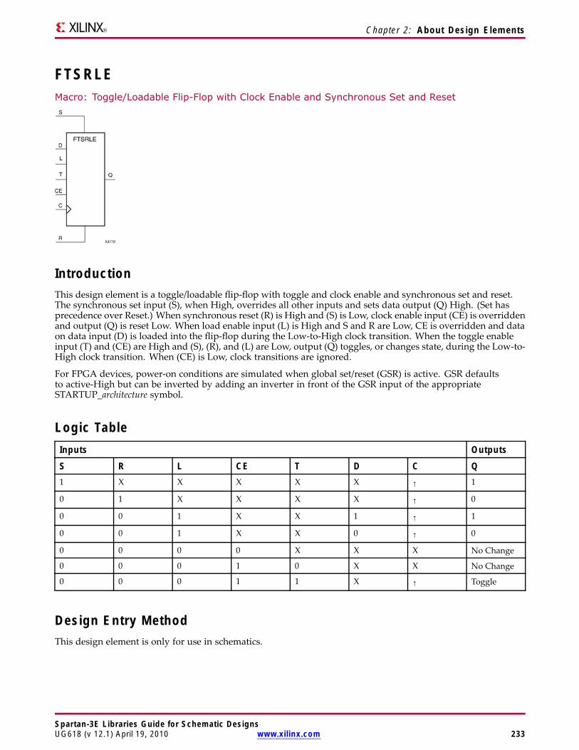
Chapter 2: About Design Elements
FTSRLEMacro: Toggle/Loadable Flip-Flop with Clock Enable and Synchronous Set and Reset
IntroductionThis design element is a toggle/loadable flip-flop with toggle and clock enable and synchronous set and reset.The synchronous set input (S), when High, overrides all other inputs and sets data output (Q) High. (Set hasprecedence over Reset.) When synchronous reset (R) is High and (S) is Low, clock enable input (CE) is overriddenand output (Q) is reset Low. When load enable input (L) is High and S and R are Low, CE is overridden and dataon data input (D) is loaded into the flip-flop during the Low-to-High clock transition. When the toggle enableinput (T) and (CE) are High and (S), (R), and (L) are Low, output (Q) toggles, or changes state, during the Low-to-High clock transition. When (CE) is Low, clock transitions are ignored.
For FPGA devices, power-on conditions are simulated when global set/reset (GSR) is active. GSR defaultsto active-High but can be inverted by adding an inverter in front of the GSR input of the appropriateSTARTUP_architecture symbol.
Logic TableInputs Outputs
S R L CE T D C Q1 X X X X X ↑ 1
0 1 X X X X ↑ 0
0 0 1 X X 1 ↑ 1
0 0 1 X X 0 ↑ 0
0 0 0 0 X X X No Change
0 0 0 1 0 X X No Change
0 0 0 1 1 X ↑ Toggle
Design Entry MethodThis design element is only for use in schematics.
Spartan-3E Libraries Guide for Schematic DesignsUG618 (v 12.1) April 19, 2010 www.xilinx.com 233
Chapter 2: About Design Elements
Available Attributes
Attribute TypeAllowedValues Default Description
INIT Binary 0, 1 1 Sets the initial value of Q output after configuration
For More Information• See the Spartan-3 Generation FPGA User Guide.
• See the Spartan-3E FPGA Family Complete Data Sheet.
Spartan-3E Libraries Guide for Schematic Designs234 www.xilinx.com UG618 (v 12.1) April 19, 2010
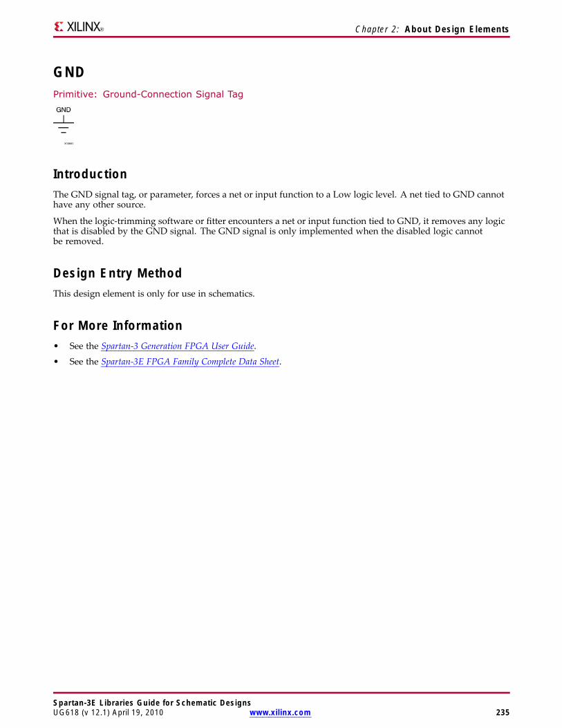
Chapter 2: About Design Elements
GNDPrimitive: Ground-Connection Signal Tag
IntroductionThe GND signal tag, or parameter, forces a net or input function to a Low logic level. A net tied to GND cannothave any other source.
When the logic-trimming software or fitter encounters a net or input function tied to GND, it removes any logicthat is disabled by the GND signal. The GND signal is only implemented when the disabled logic cannotbe removed.
Design Entry MethodThis design element is only for use in schematics.
For More Information• See the Spartan-3 Generation FPGA User Guide.
• See the Spartan-3E FPGA Family Complete Data Sheet.
Spartan-3E Libraries Guide for Schematic DesignsUG618 (v 12.1) April 19, 2010 www.xilinx.com 235
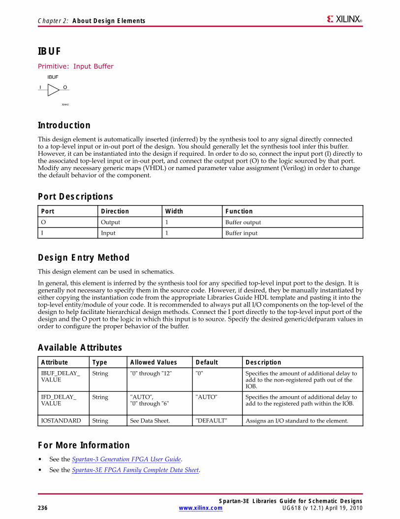
Chapter 2: About Design Elements
IBUFPrimitive: Input Buffer
IntroductionThis design element is automatically inserted (inferred) by the synthesis tool to any signal directly connectedto a top-level input or in-out port of the design. You should generally let the synthesis tool infer this buffer.However, it can be instantiated into the design if required. In order to do so, connect the input port (I) directly tothe associated top-level input or in-out port, and connect the output port (O) to the logic sourced by that port.Modify any necessary generic maps (VHDL) or named parameter value assignment (Verilog) in order to changethe default behavior of the component.
Port DescriptionsPort Direction Width FunctionO Output 1 Buffer output
I Input 1 Buffer input
Design Entry MethodThis design element can be used in schematics.
In general, this element is inferred by the synthesis tool for any specified top-level input port to the design. It isgenerally not necessary to specify them in the source code. However, if desired, they be manually instantiated byeither copying the instantiation code from the appropriate Libraries Guide HDL template and pasting it into thetop-level entity/module of your code. It is recommended to always put all I/O components on the top-level of thedesign to help facilitate hierarchical design methods. Connect the I port directly to the top-level input port of thedesign and the O port to the logic in which this input is to source. Specify the desired generic/defparam values inorder to configure the proper behavior of the buffer.
Available AttributesAttribute Type Allowed Values Default DescriptionIBUF_DELAY_VALUE
String "0" through "12" "0" Specifies the amount of additional delay toadd to the non-registered path out of theIOB.
IFD_DELAY_VALUE
String "AUTO","0" through "6"
"AUTO" Specifies the amount of additional delay toadd to the registered path within the IOB.
IOSTANDARD String See Data Sheet. "DEFAULT" Assigns an I/O standard to the element.
For More Information• See the Spartan-3 Generation FPGA User Guide.• See the Spartan-3E FPGA Family Complete Data Sheet.
Spartan-3E Libraries Guide for Schematic Designs236 www.xilinx.com UG618 (v 12.1) April 19, 2010
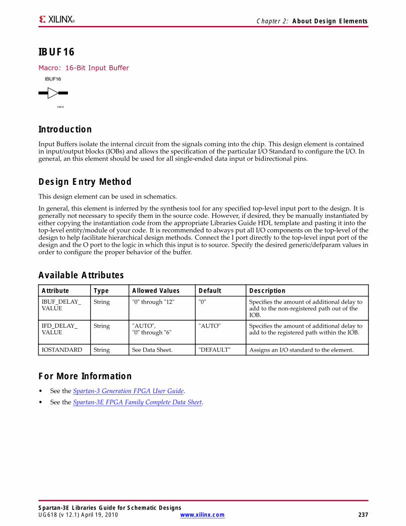
Chapter 2: About Design Elements
IBUF16Macro: 16-Bit Input Buffer
IntroductionInput Buffers isolate the internal circuit from the signals coming into the chip. This design element is containedin input/output blocks (IOBs) and allows the specification of the particular I/O Standard to configure the I/O. Ingeneral, an this element should be used for all single-ended data input or bidirectional pins.
Design Entry MethodThis design element can be used in schematics.
In general, this element is inferred by the synthesis tool for any specified top-level input port to the design. It isgenerally not necessary to specify them in the source code. However, if desired, they be manually instantiated byeither copying the instantiation code from the appropriate Libraries Guide HDL template and pasting it into thetop-level entity/module of your code. It is recommended to always put all I/O components on the top-level of thedesign to help facilitate hierarchical design methods. Connect the I port directly to the top-level input port of thedesign and the O port to the logic in which this input is to source. Specify the desired generic/defparam values inorder to configure the proper behavior of the buffer.
Available AttributesAttribute Type Allowed Values Default DescriptionIBUF_DELAY_VALUE
String "0" through "12" "0" Specifies the amount of additional delay toadd to the non-registered path out of theIOB.
IFD_DELAY_VALUE
String "AUTO","0" through "6"
"AUTO" Specifies the amount of additional delay toadd to the registered path within the IOB.
IOSTANDARD String See Data Sheet. "DEFAULT" Assigns an I/O standard to the element.
For More Information• See the Spartan-3 Generation FPGA User Guide.
• See the Spartan-3E FPGA Family Complete Data Sheet.
Spartan-3E Libraries Guide for Schematic DesignsUG618 (v 12.1) April 19, 2010 www.xilinx.com 237
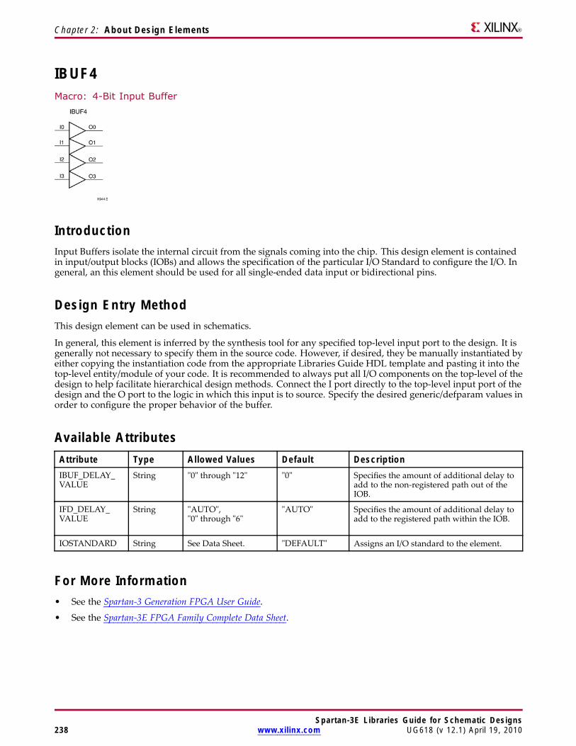
Chapter 2: About Design Elements
IBUF4Macro: 4-Bit Input Buffer
IntroductionInput Buffers isolate the internal circuit from the signals coming into the chip. This design element is containedin input/output blocks (IOBs) and allows the specification of the particular I/O Standard to configure the I/O. Ingeneral, an this element should be used for all single-ended data input or bidirectional pins.
Design Entry MethodThis design element can be used in schematics.
In general, this element is inferred by the synthesis tool for any specified top-level input port to the design. It isgenerally not necessary to specify them in the source code. However, if desired, they be manually instantiated byeither copying the instantiation code from the appropriate Libraries Guide HDL template and pasting it into thetop-level entity/module of your code. It is recommended to always put all I/O components on the top-level of thedesign to help facilitate hierarchical design methods. Connect the I port directly to the top-level input port of thedesign and the O port to the logic in which this input is to source. Specify the desired generic/defparam values inorder to configure the proper behavior of the buffer.
Available AttributesAttribute Type Allowed Values Default DescriptionIBUF_DELAY_VALUE
String "0" through "12" "0" Specifies the amount of additional delay toadd to the non-registered path out of theIOB.
IFD_DELAY_VALUE
String "AUTO","0" through "6"
"AUTO" Specifies the amount of additional delay toadd to the registered path within the IOB.
IOSTANDARD String See Data Sheet. "DEFAULT" Assigns an I/O standard to the element.
For More Information• See the Spartan-3 Generation FPGA User Guide.
• See the Spartan-3E FPGA Family Complete Data Sheet.
Spartan-3E Libraries Guide for Schematic Designs238 www.xilinx.com UG618 (v 12.1) April 19, 2010
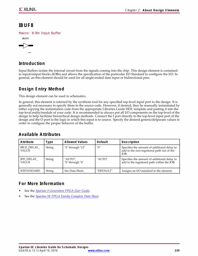
Chapter 2: About Design Elements
IBUF8Macro: 8-Bit Input Buffer
IntroductionInput Buffers isolate the internal circuit from the signals coming into the chip. This design element is containedin input/output blocks (IOBs) and allows the specification of the particular I/O Standard to configure the I/O. Ingeneral, an this element should be used for all single-ended data input or bidirectional pins.
Design Entry MethodThis design element can be used in schematics.
In general, this element is inferred by the synthesis tool for any specified top-level input port to the design. It isgenerally not necessary to specify them in the source code. However, if desired, they be manually instantiated byeither copying the instantiation code from the appropriate Libraries Guide HDL template and pasting it into thetop-level entity/module of your code. It is recommended to always put all I/O components on the top-level of thedesign to help facilitate hierarchical design methods. Connect the I port directly to the top-level input port of thedesign and the O port to the logic in which this input is to source. Specify the desired generic/defparam values inorder to configure the proper behavior of the buffer.
Available AttributesAttribute Type Allowed Values Default DescriptionIBUF_DELAY_VALUE
String "0" through "12" "0" Specifies the amount of additional delay toadd to the non-registered path out of theIOB.
IFD_DELAY_VALUE
String "AUTO","0" through "6"
"AUTO" Specifies the amount of additional delay toadd to the registered path within the IOB.
IOSTANDARD String See Data Sheet. "DEFAULT" Assigns an I/O standard to the element.
For More Information• See the Spartan-3 Generation FPGA User Guide.
• See the Spartan-3E FPGA Family Complete Data Sheet.
Spartan-3E Libraries Guide for Schematic DesignsUG618 (v 12.1) April 19, 2010 www.xilinx.com 239
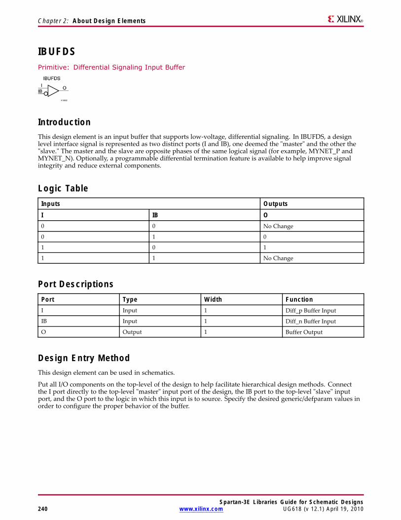
Chapter 2: About Design Elements
IBUFDSPrimitive: Differential Signaling Input Buffer
IntroductionThis design element is an input buffer that supports low-voltage, differential signaling. In IBUFDS, a designlevel interface signal is represented as two distinct ports (I and IB), one deemed the "master" and the other the"slave." The master and the slave are opposite phases of the same logical signal (for example, MYNET_P andMYNET_N). Optionally, a programmable differential termination feature is available to help improve signalintegrity and reduce external components.
Logic TableInputs Outputs
I IB O0 0 No Change
0 1 0
1 0 1
1 1 No Change
Port DescriptionsPort Type Width FunctionI Input 1 Diff_p Buffer Input
IB Input 1 Diff_n Buffer Input
O Output 1 Buffer Output
Design Entry MethodThis design element can be used in schematics.
Put all I/O components on the top-level of the design to help facilitate hierarchical design methods. Connectthe I port directly to the top-level "master" input port of the design, the IB port to the top-level "slave" inputport, and the O port to the logic in which this input is to source. Specify the desired generic/defparam values inorder to configure the proper behavior of the buffer.
Spartan-3E Libraries Guide for Schematic Designs240 www.xilinx.com UG618 (v 12.1) April 19, 2010
Chapter 2: About Design Elements
Available Attributes
Attribute TypeAllowedValues Default Description
DIFF_TERM Boolean TRUE or FALSE FALSE Enables the built-in differential terminationresistor.
IBUF_DELAY_VALUE
String "0" through "12" "0" Specifies the amount of additional delay to add tothe non-registered path out of the IOB.
IFD_DELAY_VALUE
String "AUTO","0" thru "6"
"AUTO" Specifies the amount of additional delay to add tothe registered path within the IOB.
IOSTANDARD String See Data Sheet. "DEFAULT" Assigns an I/O standard to the element.
For More Information• See the Spartan-3 Generation FPGA User Guide.
• See the Spartan-3E FPGA Family Complete Data Sheet.
Spartan-3E Libraries Guide for Schematic DesignsUG618 (v 12.1) April 19, 2010 www.xilinx.com 241
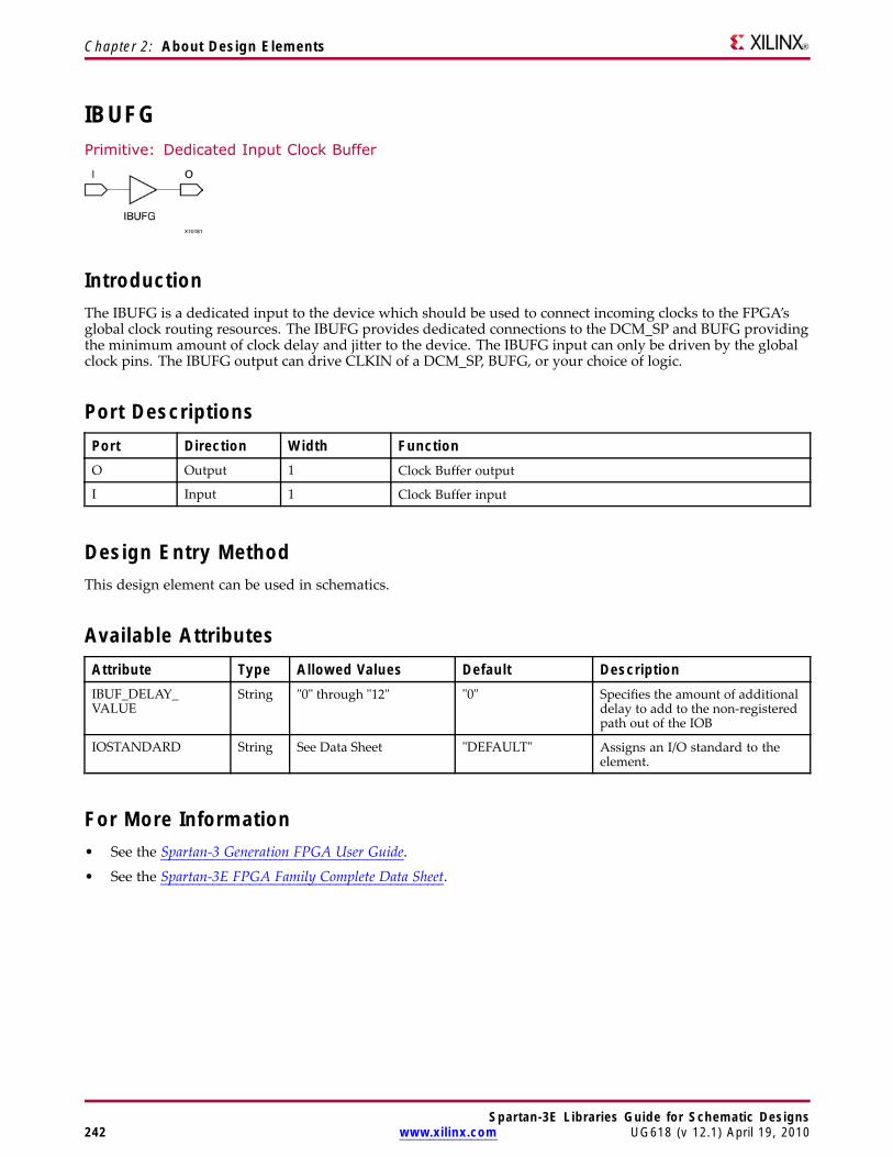
Chapter 2: About Design Elements
IBUFGPrimitive: Dedicated Input Clock Buffer
IntroductionThe IBUFG is a dedicated input to the device which should be used to connect incoming clocks to the FPGA’sglobal clock routing resources. The IBUFG provides dedicated connections to the DCM_SP and BUFG providingthe minimum amount of clock delay and jitter to the device. The IBUFG input can only be driven by the globalclock pins. The IBUFG output can drive CLKIN of a DCM_SP, BUFG, or your choice of logic.
Port DescriptionsPort Direction Width FunctionO Output 1 Clock Buffer output
I Input 1 Clock Buffer input
Design Entry MethodThis design element can be used in schematics.
Available AttributesAttribute Type Allowed Values Default DescriptionIBUF_DELAY_VALUE
String "0" through "12" "0" Specifies the amount of additionaldelay to add to the non-registeredpath out of the IOB
IOSTANDARD String See Data Sheet "DEFAULT" Assigns an I/O standard to theelement.
For More Information• See the Spartan-3 Generation FPGA User Guide.
• See the Spartan-3E FPGA Family Complete Data Sheet.
Spartan-3E Libraries Guide for Schematic Designs242 www.xilinx.com UG618 (v 12.1) April 19, 2010
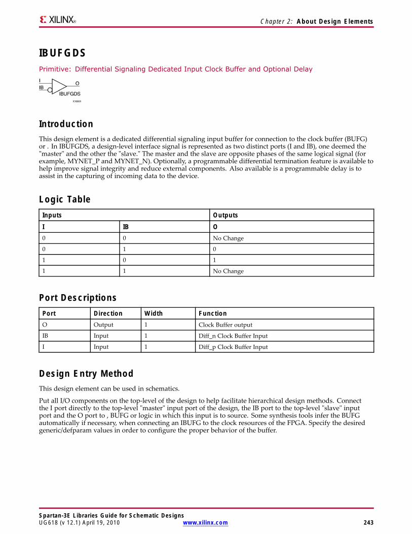
Chapter 2: About Design Elements
IBUFGDSPrimitive: Differential Signaling Dedicated Input Clock Buffer and Optional Delay
IntroductionThis design element is a dedicated differential signaling input buffer for connection to the clock buffer (BUFG)or . In IBUFGDS, a design-level interface signal is represented as two distinct ports (I and IB), one deemed the"master" and the other the "slave." The master and the slave are opposite phases of the same logical signal (forexample, MYNET_P and MYNET_N). Optionally, a programmable differential termination feature is available tohelp improve signal integrity and reduce external components. Also available is a programmable delay is toassist in the capturing of incoming data to the device.
Logic TableInputs Outputs
I IB O0 0 No Change
0 1 0
1 0 1
1 1 No Change
Port DescriptionsPort Direction Width FunctionO Output 1 Clock Buffer output
IB Input 1 Diff_n Clock Buffer Input
I Input 1 Diff_p Clock Buffer Input
Design Entry MethodThis design element can be used in schematics.
Put all I/O components on the top-level of the design to help facilitate hierarchical design methods. Connectthe I port directly to the top-level "master" input port of the design, the IB port to the top-level "slave" inputport and the O port to , BUFG or logic in which this input is to source. Some synthesis tools infer the BUFGautomatically if necessary, when connecting an IBUFG to the clock resources of the FPGA. Specify the desiredgeneric/defparam values in order to configure the proper behavior of the buffer.
Spartan-3E Libraries Guide for Schematic DesignsUG618 (v 12.1) April 19, 2010 www.xilinx.com 243
Chapter 2: About Design Elements
Available Attributes
Attribute TypeAllowedValues Default Description
DIFF_TERM Boolean TRUE or FALSE FALSE Enables the built-in differentialtermination resistor.
IBUF_DELAY_VALUE
String "0" through "12" "0" Specifies the amount of additionaldelay to add to the non-registeredpath out of the IOB
IOSTANDARD String See Data Sheet "DEFAULT" Assigns an I/O standard to theelement.
For More Information• See the Spartan-3 Generation FPGA User Guide.
• See the Spartan-3E FPGA Family Complete Data Sheet.
Spartan-3E Libraries Guide for Schematic Designs244 www.xilinx.com UG618 (v 12.1) April 19, 2010
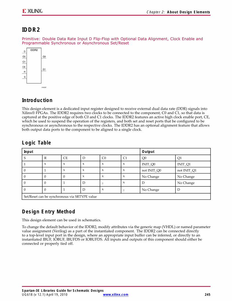
Chapter 2: About Design Elements
IDDR2Primitive: Double Data Rate Input D Flip-Flop with Optional Data Alignment, Clock Enable andProgrammable Synchronous or Asynchronous Set/Reset
IntroductionThis design element is a dedicated input register designed to receive external dual data rate (DDR) signals intoXilinx® FPGAs. The IDDR2 requires two clocks to be connected to the component, C0 and C1, so that data iscaptured at the positive edge of both C0 and C1 clocks. The IDDR2 features an active high clock enable port, CE,which be used to suspend the operation of the registers, and both set and reset ports that be configured to besynchronous or asynchronous to the respective clocks. The IDDR2 has an optional alignment feature that allowsboth output data ports to the component to be aligned to a single clock.
Logic TableInput OutputS R CE D C0 C1 Q0 Q1
1 x x x x x INIT_Q0 INIT_Q1
0 1 x x x x not INIT_Q0 not INIT_Q1
0 0 0 x x x No Change No Change
0 0 1 D ↑ x D No Change
0 0 1 D x ↑ No Change D
Set/Reset can be synchronous via SRTYPE value
Design Entry MethodThis design element can be used in schematics.
To change the default behavior of the IDDR2, modify attributes via the generic map (VHDL) or named parametervalue assignment (Verilog) as a part of the instantiated component. The IDDR2 can be connected directlyto a top-level input port in the design, where an appropriate input buffer can be inferred, or directly to aninstantiated IBUF, IOBUF, IBUFDS or IOBUFDS. All inputs and outputs of this component should either beconnected or properly tied off.
Spartan-3E Libraries Guide for Schematic DesignsUG618 (v 12.1) April 19, 2010 www.xilinx.com 245
Chapter 2: About Design Elements
Available AttributesAttribute Type Allowed Values Default DescriptionDDR_ALIGNMENT String NONE, "C0", "C1” “NONE” Sets the output alignment more for the DDR register
• NONE - Makes the data available on the Q0 andQ1 outputs shortly after the corresponding C0 orC1 positive clock edge.
• C0 – Makes the data on both Q0 and Q1 align tothe positive edge of the C0 clock.
• C1 - Makes the data on both Q0 and Q1 align tothe positive edge of the C1 clock.
INIT_Q0 Integer 0, 1 0 Sets initial state of the Q0 output to 0 or 1.
INIT_Q1 Integer 0, 1 0 Sets initial state of the Q1 output to 0 or 1.
SRTYPE String "SYNC", "ASYNC” "SYNC” Specifies SYNC" or "ASYNC" set/reset.
For More InformationSee the Spartan-3 Generation FPGA User Guide.
Spartan-3E Libraries Guide for Schematic Designs246 www.xilinx.com UG618 (v 12.1) April 19, 2010
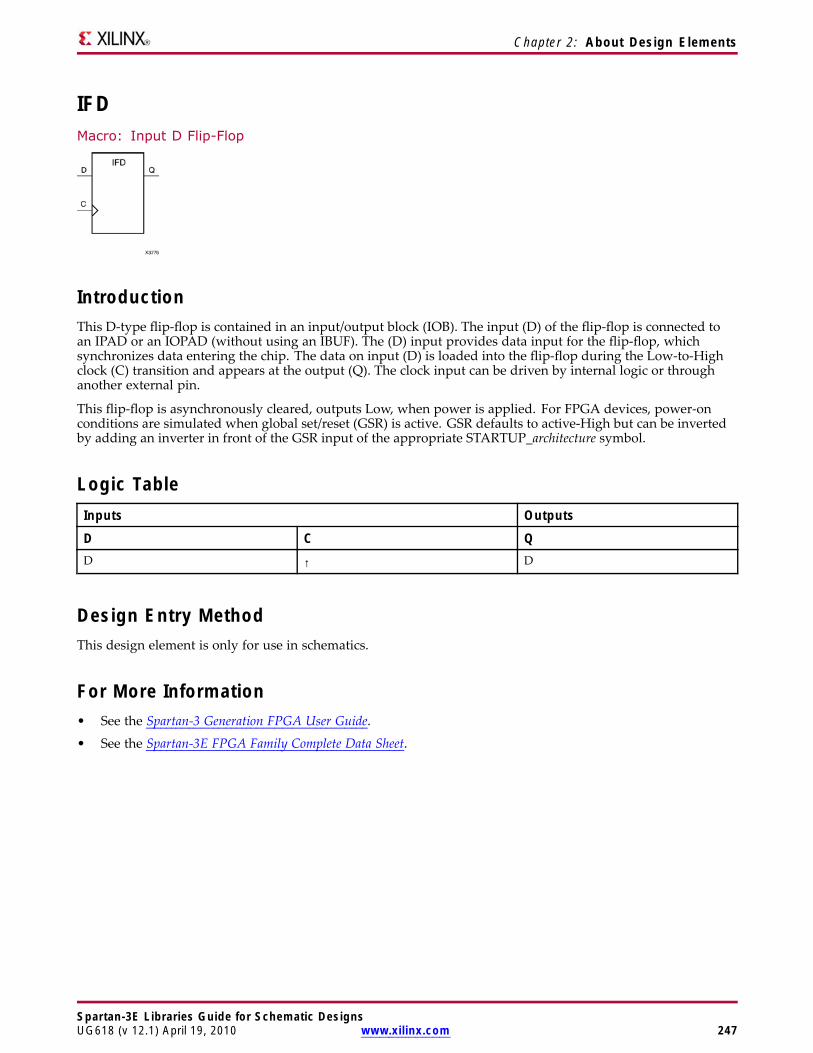
Chapter 2: About Design Elements
IFDMacro: Input D Flip-Flop
IntroductionThis D-type flip-flop is contained in an input/output block (IOB). The input (D) of the flip-flop is connected toan IPAD or an IOPAD (without using an IBUF). The (D) input provides data input for the flip-flop, whichsynchronizes data entering the chip. The data on input (D) is loaded into the flip-flop during the Low-to-Highclock (C) transition and appears at the output (Q). The clock input can be driven by internal logic or throughanother external pin.
This flip-flop is asynchronously cleared, outputs Low, when power is applied. For FPGA devices, power-onconditions are simulated when global set/reset (GSR) is active. GSR defaults to active-High but can be invertedby adding an inverter in front of the GSR input of the appropriate STARTUP_architecture symbol.
Logic TableInputs Outputs
D C QD ↑ D
Design Entry MethodThis design element is only for use in schematics.
For More Information• See the Spartan-3 Generation FPGA User Guide.
• See the Spartan-3E FPGA Family Complete Data Sheet.
Spartan-3E Libraries Guide for Schematic DesignsUG618 (v 12.1) April 19, 2010 www.xilinx.com 247
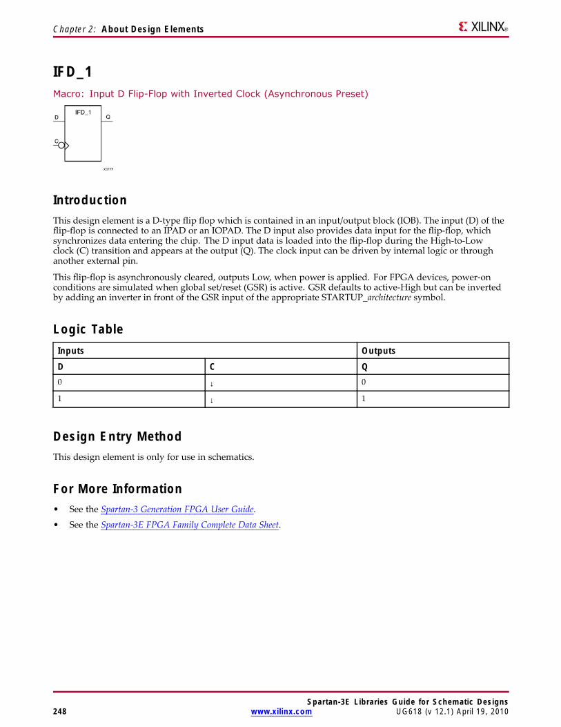
Chapter 2: About Design Elements
IFD_1Macro: Input D Flip-Flop with Inverted Clock (Asynchronous Preset)
IntroductionThis design element is a D-type flip flop which is contained in an input/output block (IOB). The input (D) of theflip-flop is connected to an IPAD or an IOPAD. The D input also provides data input for the flip-flop, whichsynchronizes data entering the chip. The D input data is loaded into the flip-flop during the High-to-Lowclock (C) transition and appears at the output (Q). The clock input can be driven by internal logic or throughanother external pin.
This flip-flop is asynchronously cleared, outputs Low, when power is applied. For FPGA devices, power-onconditions are simulated when global set/reset (GSR) is active. GSR defaults to active-High but can be invertedby adding an inverter in front of the GSR input of the appropriate STARTUP_architecture symbol.
Logic TableInputs Outputs
D C Q0 ↓ 0
1 ↓ 1
Design Entry MethodThis design element is only for use in schematics.
For More Information• See the Spartan-3 Generation FPGA User Guide.
• See the Spartan-3E FPGA Family Complete Data Sheet.
Spartan-3E Libraries Guide for Schematic Designs248 www.xilinx.com UG618 (v 12.1) April 19, 2010
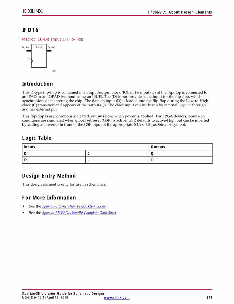
Chapter 2: About Design Elements
IFD16Macro: 16-Bit Input D Flip-Flop
IntroductionThis D-type flip-flop is contained in an input/output block (IOB). The input (D) of the flip-flop is connected toan IPAD or an IOPAD (without using an IBUF). The (D) input provides data input for the flip-flop, whichsynchronizes data entering the chip. The data on input (D) is loaded into the flip-flop during the Low-to-Highclock (C) transition and appears at the output (Q). The clock input can be driven by internal logic or throughanother external pin.
This flip-flop is asynchronously cleared, outputs Low, when power is applied. For FPGA devices, power-onconditions are simulated when global set/reset (GSR) is active. GSR defaults to active-High but can be invertedby adding an inverter in front of the GSR input of the appropriate STARTUP_architecture symbol.
Logic TableInputs Outputs
D C QD ↑ D
Design Entry MethodThis design element is only for use in schematics.
For More Information• See the Spartan-3 Generation FPGA User Guide.
• See the Spartan-3E FPGA Family Complete Data Sheet.
Spartan-3E Libraries Guide for Schematic DesignsUG618 (v 12.1) April 19, 2010 www.xilinx.com 249
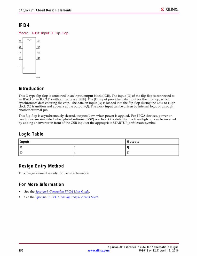
Chapter 2: About Design Elements
IFD4Macro: 4-Bit Input D Flip-Flop
IntroductionThis D-type flip-flop is contained in an input/output block (IOB). The input (D) of the flip-flop is connected toan IPAD or an IOPAD (without using an IBUF). The (D) input provides data input for the flip-flop, whichsynchronizes data entering the chip. The data on input (D) is loaded into the flip-flop during the Low-to-Highclock (C) transition and appears at the output (Q). The clock input can be driven by internal logic or throughanother external pin.
This flip-flop is asynchronously cleared, outputs Low, when power is applied. For FPGA devices, power-onconditions are simulated when global set/reset (GSR) is active. GSR defaults to active-High but can be invertedby adding an inverter in front of the GSR input of the appropriate STARTUP_architecture symbol.
Logic TableInputs Outputs
D C QD ↑ D
Design Entry MethodThis design element is only for use in schematics.
For More Information• See the Spartan-3 Generation FPGA User Guide.
• See the Spartan-3E FPGA Family Complete Data Sheet.
Spartan-3E Libraries Guide for Schematic Designs250 www.xilinx.com UG618 (v 12.1) April 19, 2010
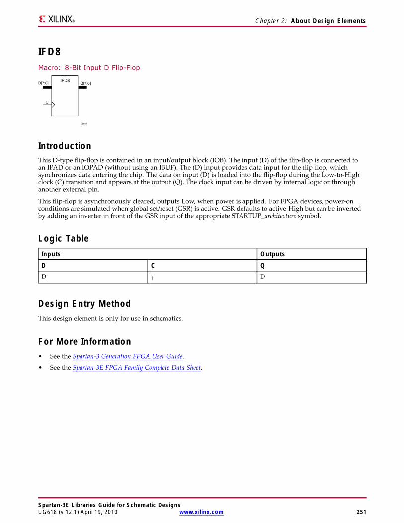
Chapter 2: About Design Elements
IFD8Macro: 8-Bit Input D Flip-Flop
IntroductionThis D-type flip-flop is contained in an input/output block (IOB). The input (D) of the flip-flop is connected toan IPAD or an IOPAD (without using an IBUF). The (D) input provides data input for the flip-flop, whichsynchronizes data entering the chip. The data on input (D) is loaded into the flip-flop during the Low-to-Highclock (C) transition and appears at the output (Q). The clock input can be driven by internal logic or throughanother external pin.
This flip-flop is asynchronously cleared, outputs Low, when power is applied. For FPGA devices, power-onconditions are simulated when global set/reset (GSR) is active. GSR defaults to active-High but can be invertedby adding an inverter in front of the GSR input of the appropriate STARTUP_architecture symbol.
Logic TableInputs Outputs
D C QD ↑ D
Design Entry MethodThis design element is only for use in schematics.
For More Information• See the Spartan-3 Generation FPGA User Guide.
• See the Spartan-3E FPGA Family Complete Data Sheet.
Spartan-3E Libraries Guide for Schematic DesignsUG618 (v 12.1) April 19, 2010 www.xilinx.com 251
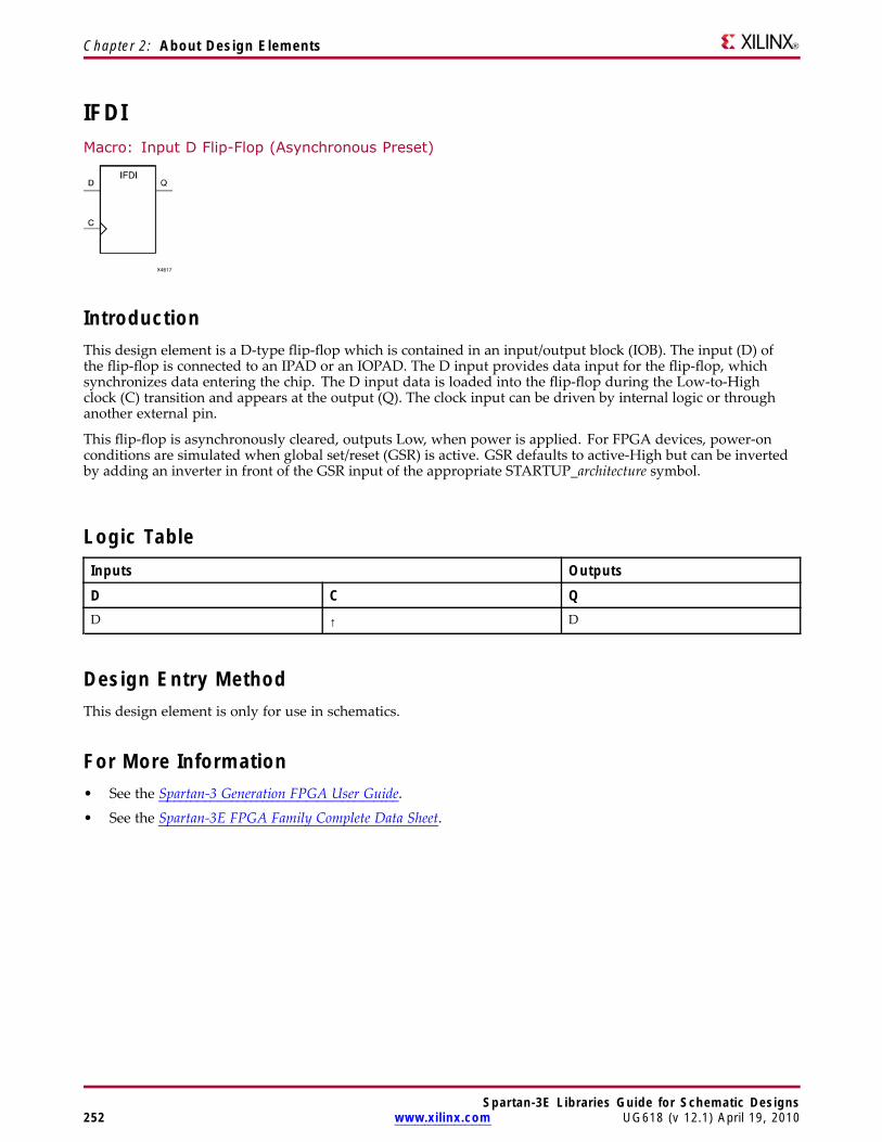
Chapter 2: About Design Elements
IFDIMacro: Input D Flip-Flop (Asynchronous Preset)
IntroductionThis design element is a D-type flip-flop which is contained in an input/output block (IOB). The input (D) ofthe flip-flop is connected to an IPAD or an IOPAD. The D input provides data input for the flip-flop, whichsynchronizes data entering the chip. The D input data is loaded into the flip-flop during the Low-to-Highclock (C) transition and appears at the output (Q). The clock input can be driven by internal logic or throughanother external pin.
This flip-flop is asynchronously cleared, outputs Low, when power is applied. For FPGA devices, power-onconditions are simulated when global set/reset (GSR) is active. GSR defaults to active-High but can be invertedby adding an inverter in front of the GSR input of the appropriate STARTUP_architecture symbol.
Logic TableInputs Outputs
D C QD ↑ D
Design Entry MethodThis design element is only for use in schematics.
For More Information• See the Spartan-3 Generation FPGA User Guide.
• See the Spartan-3E FPGA Family Complete Data Sheet.
Spartan-3E Libraries Guide for Schematic Designs252 www.xilinx.com UG618 (v 12.1) April 19, 2010
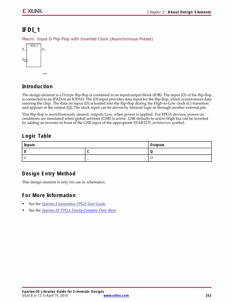
Chapter 2: About Design Elements
IFDI_1Macro: Input D Flip-Flop with Inverted Clock (Asynchronous Preset)
IntroductionThe design element is a D-type flip-flop is contained in an input/output block (IOB). The input (D) of the flip-flopis connected to an IPAD or an IOPAD. The (D) input provides data input for the flip-flop, which synchronizes dataentering the chip. The data on input (D) is loaded into the flip-flop during the High-to-Low clock (C) transitionand appears at the output (Q). The clock input can be driven by internal logic or through another external pin.
This flip-flop is asynchronously cleared, outputs Low, when power is applied. For FPGA devices, power-onconditions are simulated when global set/reset (GSR) is active. GSR defaults to active-High but can be invertedby adding an inverter in front of the GSR input of the appropriate STARTUP_architecture symbol.
Logic TableInputs Outputs
D C Q0 ↓ D
Design Entry MethodThis design element is only for use in schematics.
For More Information• See the Spartan-3 Generation FPGA User Guide.
• See the Spartan-3E FPGA Family Complete Data Sheet.
Spartan-3E Libraries Guide for Schematic DesignsUG618 (v 12.1) April 19, 2010 www.xilinx.com 253

Chapter 2: About Design Elements
IFDXMacro: Input D Flip-Flop with Clock Enable
IntroductionThis D-type flip-flop is contained in an input/output block (IOB). The input (D) of the flip-flop is connectedto an IPAD or an IOPAD (without using an IBUF). The D input provides data input for the flip-flop, whichsynchronizes data entering the chip. When CE is High, the data on input D is loaded into the flip-flop during theLow-to-High clock (C) transition and appears at the output (Q). The clock input can be driven by internal logic orthrough another external pin. When CE is Low, flip-flop outputs do not change.
This flip-flop is asynchronously cleared, outputs Low, when power is applied. For FPGA devices, power-onconditions are simulated when global set/reset (GSR) is active. GSR defaults to active-High but can be invertedby adding an inverter in front of the GSR input of the appropriate STARTUP_architecture symbol.
Logic TableInputs Outputs
CE D C Q1 D ↑ D
0 X X No Change
Design Entry MethodThis design element is only for use in schematics.
For More Information• See the Spartan-3 Generation FPGA User Guide.
• See the Spartan-3E FPGA Family Complete Data Sheet.
Spartan-3E Libraries Guide for Schematic Designs254 www.xilinx.com UG618 (v 12.1) April 19, 2010
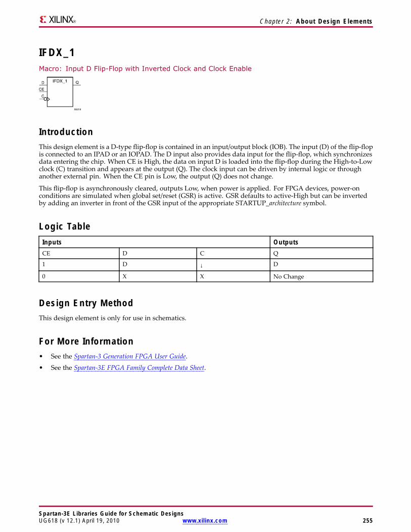
Chapter 2: About Design Elements
IFDX_1Macro: Input D Flip-Flop with Inverted Clock and Clock Enable
IntroductionThis design element is a D-type flip-flop is contained in an input/output block (IOB). The input (D) of the flip-flopis connected to an IPAD or an IOPAD. The D input also provides data input for the flip-flop, which synchronizesdata entering the chip. When CE is High, the data on input D is loaded into the flip-flop during the High-to-Lowclock (C) transition and appears at the output (Q). The clock input can be driven by internal logic or throughanother external pin. When the CE pin is Low, the output (Q) does not change.
This flip-flop is asynchronously cleared, outputs Low, when power is applied. For FPGA devices, power-onconditions are simulated when global set/reset (GSR) is active. GSR defaults to active-High but can be invertedby adding an inverter in front of the GSR input of the appropriate STARTUP_architecture symbol.
Logic TableInputs OutputsCE D C Q
1 D ↓ D
0 X X No Change
Design Entry MethodThis design element is only for use in schematics.
For More Information• See the Spartan-3 Generation FPGA User Guide.
• See the Spartan-3E FPGA Family Complete Data Sheet.
Spartan-3E Libraries Guide for Schematic DesignsUG618 (v 12.1) April 19, 2010 www.xilinx.com 255

Chapter 2: About Design Elements
IFDX16Macro: 16-Bit Input D Flip-Flops with Clock Enable
IntroductionThis D-type flip-flop is contained in an input/output block (IOB). The input (D) of the flip-flop is connectedto an IPAD or an IOPAD (without using an IBUF). The D input provides data input for the flip-flop, whichsynchronizes data entering the chip. When CE is High, the data on input D is loaded into the flip-flop during theLow-to-High clock (C) transition and appears at the output (Q). The clock input can be driven by internal logic orthrough another external pin. When CE is Low, flip-flop outputs do not change.
This flip-flop is asynchronously cleared, outputs Low, when power is applied. For FPGA devices, power-onconditions are simulated when global set/reset (GSR) is active. GSR defaults to active-High but can be invertedby adding an inverter in front of the GSR input of the appropriate STARTUP_architecture symbol.
Logic TableInputs Outputs
CE D C Q1 D ↑ D
0 X X No Change
Design Entry MethodThis design element is only for use in schematics.
For More Information• See the Spartan-3 Generation FPGA User Guide.
• See the Spartan-3E FPGA Family Complete Data Sheet.
Spartan-3E Libraries Guide for Schematic Designs256 www.xilinx.com UG618 (v 12.1) April 19, 2010
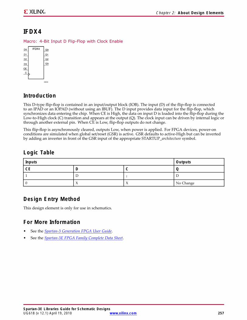
Chapter 2: About Design Elements
IFDX4Macro: 4-Bit Input D Flip-Flop with Clock Enable
IntroductionThis D-type flip-flop is contained in an input/output block (IOB). The input (D) of the flip-flop is connectedto an IPAD or an IOPAD (without using an IBUF). The D input provides data input for the flip-flop, whichsynchronizes data entering the chip. When CE is High, the data on input D is loaded into the flip-flop during theLow-to-High clock (C) transition and appears at the output (Q). The clock input can be driven by internal logic orthrough another external pin. When CE is Low, flip-flop outputs do not change.
This flip-flop is asynchronously cleared, outputs Low, when power is applied. For FPGA devices, power-onconditions are simulated when global set/reset (GSR) is active. GSR defaults to active-High but can be invertedby adding an inverter in front of the GSR input of the appropriate STARTUP_architecture symbol.
Logic TableInputs Outputs
CE D C Q1 D ↑ D
0 X X No Change
Design Entry MethodThis design element is only for use in schematics.
For More Information• See the Spartan-3 Generation FPGA User Guide.
• See the Spartan-3E FPGA Family Complete Data Sheet.
Spartan-3E Libraries Guide for Schematic DesignsUG618 (v 12.1) April 19, 2010 www.xilinx.com 257
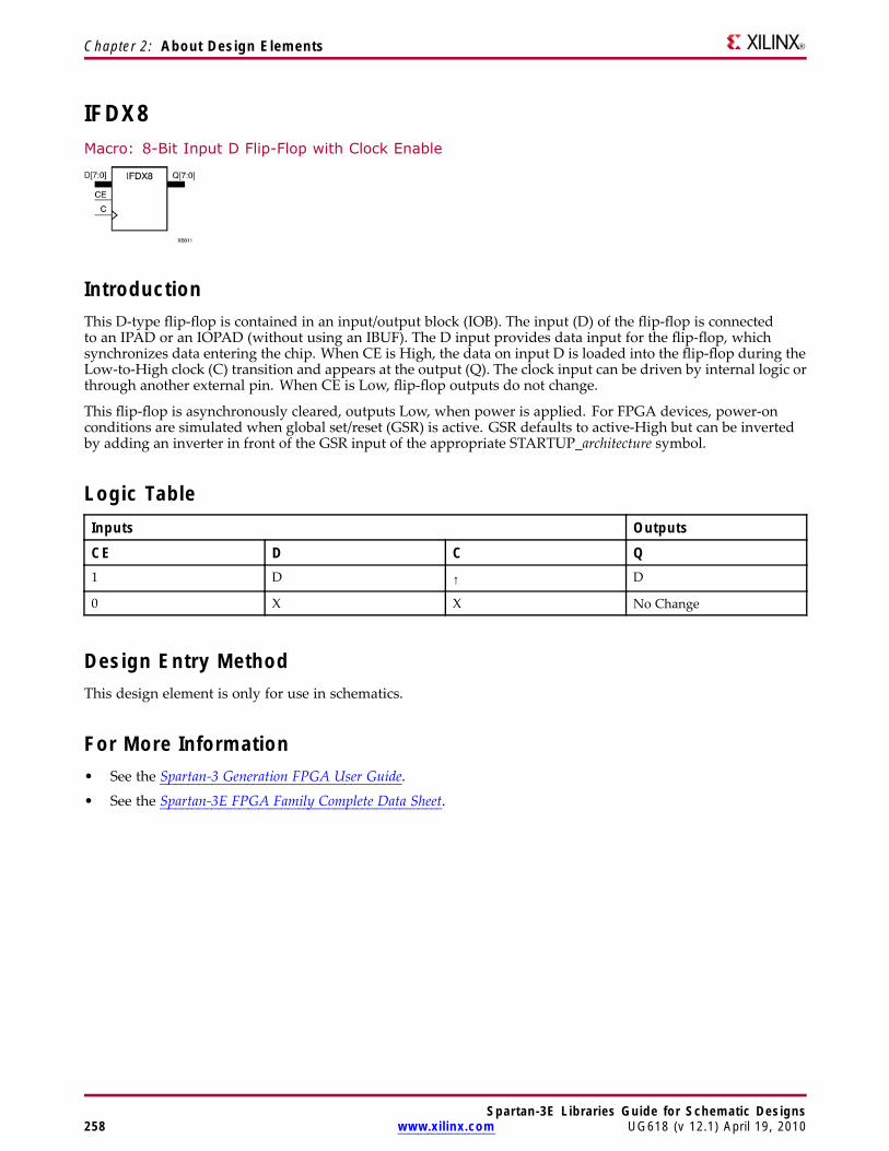
Chapter 2: About Design Elements
IFDX8Macro: 8-Bit Input D Flip-Flop with Clock Enable
IntroductionThis D-type flip-flop is contained in an input/output block (IOB). The input (D) of the flip-flop is connectedto an IPAD or an IOPAD (without using an IBUF). The D input provides data input for the flip-flop, whichsynchronizes data entering the chip. When CE is High, the data on input D is loaded into the flip-flop during theLow-to-High clock (C) transition and appears at the output (Q). The clock input can be driven by internal logic orthrough another external pin. When CE is Low, flip-flop outputs do not change.
This flip-flop is asynchronously cleared, outputs Low, when power is applied. For FPGA devices, power-onconditions are simulated when global set/reset (GSR) is active. GSR defaults to active-High but can be invertedby adding an inverter in front of the GSR input of the appropriate STARTUP_architecture symbol.
Logic TableInputs Outputs
CE D C Q1 D ↑ D
0 X X No Change
Design Entry MethodThis design element is only for use in schematics.
For More Information• See the Spartan-3 Generation FPGA User Guide.
• See the Spartan-3E FPGA Family Complete Data Sheet.
Spartan-3E Libraries Guide for Schematic Designs258 www.xilinx.com UG618 (v 12.1) April 19, 2010
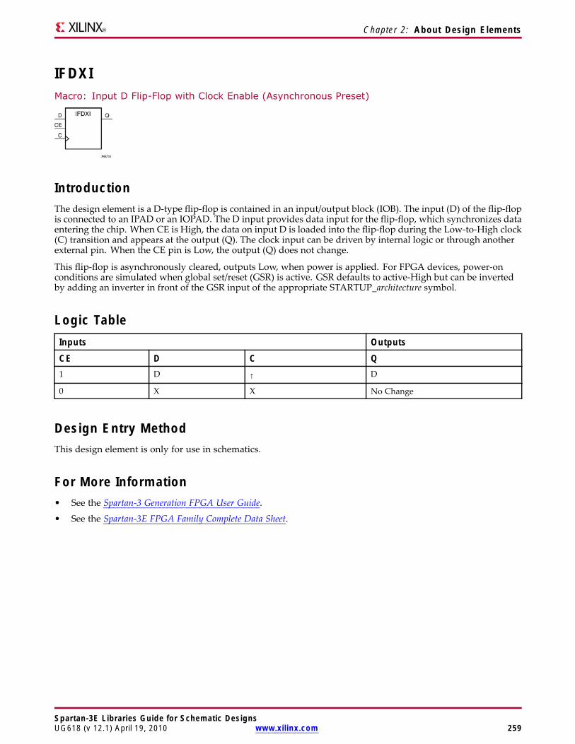
Chapter 2: About Design Elements
IFDXIMacro: Input D Flip-Flop with Clock Enable (Asynchronous Preset)
IntroductionThe design element is a D-type flip-flop is contained in an input/output block (IOB). The input (D) of the flip-flopis connected to an IPAD or an IOPAD. The D input provides data input for the flip-flop, which synchronizes dataentering the chip. When CE is High, the data on input D is loaded into the flip-flop during the Low-to-High clock(C) transition and appears at the output (Q). The clock input can be driven by internal logic or through anotherexternal pin. When the CE pin is Low, the output (Q) does not change.
This flip-flop is asynchronously cleared, outputs Low, when power is applied. For FPGA devices, power-onconditions are simulated when global set/reset (GSR) is active. GSR defaults to active-High but can be invertedby adding an inverter in front of the GSR input of the appropriate STARTUP_architecture symbol.
Logic TableInputs Outputs
CE D C Q1 D ↑ D
0 X X No Change
Design Entry MethodThis design element is only for use in schematics.
For More Information• See the Spartan-3 Generation FPGA User Guide.
• See the Spartan-3E FPGA Family Complete Data Sheet.
Spartan-3E Libraries Guide for Schematic DesignsUG618 (v 12.1) April 19, 2010 www.xilinx.com 259
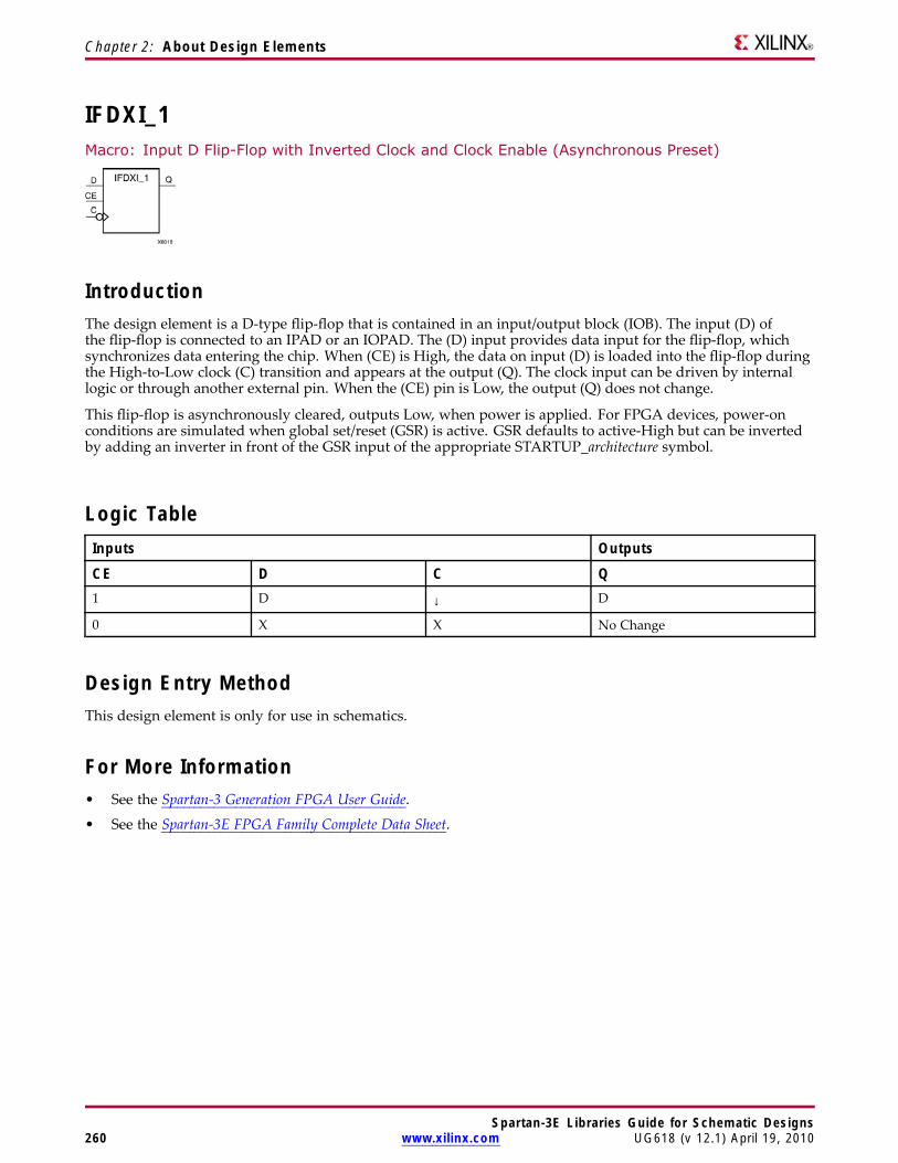
Chapter 2: About Design Elements
IFDXI_1Macro: Input D Flip-Flop with Inverted Clock and Clock Enable (Asynchronous Preset)
IntroductionThe design element is a D-type flip-flop that is contained in an input/output block (IOB). The input (D) ofthe flip-flop is connected to an IPAD or an IOPAD. The (D) input provides data input for the flip-flop, whichsynchronizes data entering the chip. When (CE) is High, the data on input (D) is loaded into the flip-flop duringthe High-to-Low clock (C) transition and appears at the output (Q). The clock input can be driven by internallogic or through another external pin. When the (CE) pin is Low, the output (Q) does not change.
This flip-flop is asynchronously cleared, outputs Low, when power is applied. For FPGA devices, power-onconditions are simulated when global set/reset (GSR) is active. GSR defaults to active-High but can be invertedby adding an inverter in front of the GSR input of the appropriate STARTUP_architecture symbol.
Logic TableInputs Outputs
CE D C Q1 D ↓ D
0 X X No Change
Design Entry MethodThis design element is only for use in schematics.
For More Information• See the Spartan-3 Generation FPGA User Guide.
• See the Spartan-3E FPGA Family Complete Data Sheet.
Spartan-3E Libraries Guide for Schematic Designs260 www.xilinx.com UG618 (v 12.1) April 19, 2010
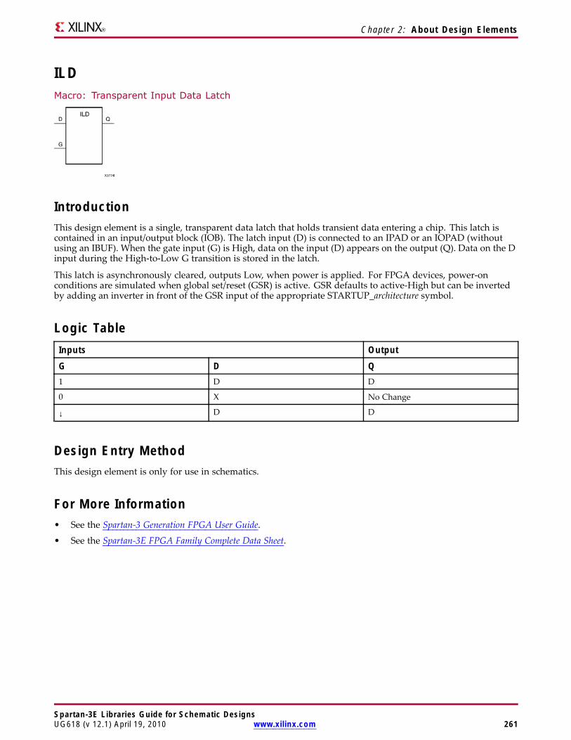
Chapter 2: About Design Elements
ILDMacro: Transparent Input Data Latch
IntroductionThis design element is a single, transparent data latch that holds transient data entering a chip. This latch iscontained in an input/output block (IOB). The latch input (D) is connected to an IPAD or an IOPAD (withoutusing an IBUF). When the gate input (G) is High, data on the input (D) appears on the output (Q). Data on the Dinput during the High-to-Low G transition is stored in the latch.
This latch is asynchronously cleared, outputs Low, when power is applied. For FPGA devices, power-onconditions are simulated when global set/reset (GSR) is active. GSR defaults to active-High but can be invertedby adding an inverter in front of the GSR input of the appropriate STARTUP_architecture symbol.
Logic TableInputs Output
G D Q1 D D
0 X No Change
↓ D D
Design Entry MethodThis design element is only for use in schematics.
For More Information• See the Spartan-3 Generation FPGA User Guide.
• See the Spartan-3E FPGA Family Complete Data Sheet.
Spartan-3E Libraries Guide for Schematic DesignsUG618 (v 12.1) April 19, 2010 www.xilinx.com 261
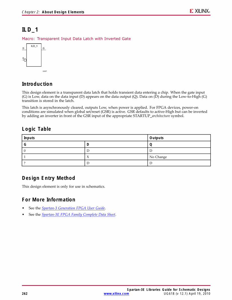
Chapter 2: About Design Elements
ILD_1Macro: Transparent Input Data Latch with Inverted Gate
IntroductionThis design element is a transparent data latch that holds transient data entering a chip. When the gate input(G) is Low, data on the data input (D) appears on the data output (Q). Data on (D) during the Low-to-High (G)transition is stored in the latch.
This latch is asynchronously cleared, outputs Low, when power is applied. For FPGA devices, power-onconditions are simulated when global set/reset (GSR) is active. GSR defaults to active-High but can be invertedby adding an inverter in front of the GSR input of the appropriate STARTUP_architecture symbol.
Logic TableInputs Outputs
G D Q0 D D
1 X No Change
? D D
Design Entry MethodThis design element is only for use in schematics.
For More Information• See the Spartan-3 Generation FPGA User Guide.
• See the Spartan-3E FPGA Family Complete Data Sheet.
Spartan-3E Libraries Guide for Schematic Designs262 www.xilinx.com UG618 (v 12.1) April 19, 2010
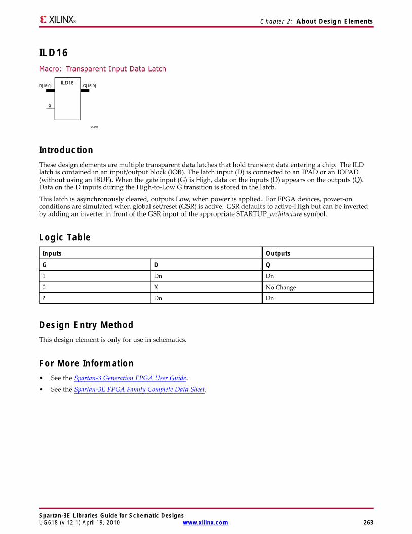
Chapter 2: About Design Elements
ILD16Macro: Transparent Input Data Latch
IntroductionThese design elements are multiple transparent data latches that hold transient data entering a chip. The ILDlatch is contained in an input/output block (IOB). The latch input (D) is connected to an IPAD or an IOPAD(without using an IBUF). When the gate input (G) is High, data on the inputs (D) appears on the outputs (Q).Data on the D inputs during the High-to-Low G transition is stored in the latch.
This latch is asynchronously cleared, outputs Low, when power is applied. For FPGA devices, power-onconditions are simulated when global set/reset (GSR) is active. GSR defaults to active-High but can be invertedby adding an inverter in front of the GSR input of the appropriate STARTUP_architecture symbol.
Logic TableInputs Outputs
G D Q1 Dn Dn
0 X No Change
? Dn Dn
Design Entry MethodThis design element is only for use in schematics.
For More Information• See the Spartan-3 Generation FPGA User Guide.
• See the Spartan-3E FPGA Family Complete Data Sheet.
Spartan-3E Libraries Guide for Schematic DesignsUG618 (v 12.1) April 19, 2010 www.xilinx.com 263
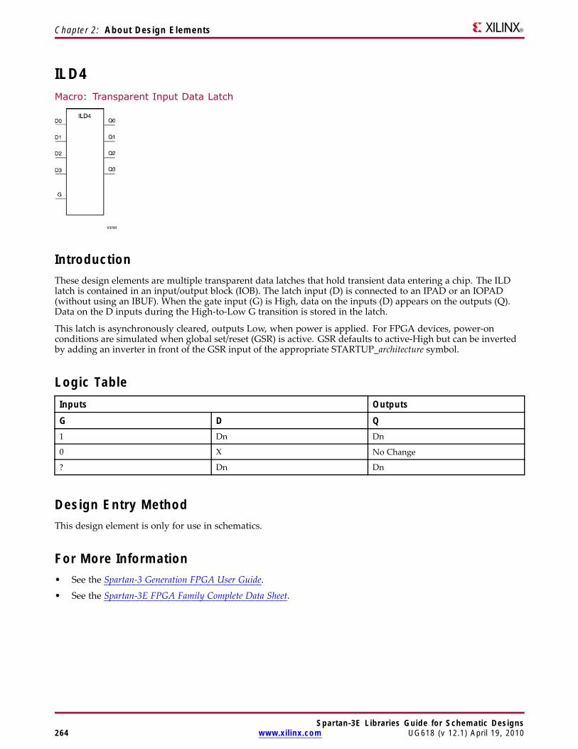
Chapter 2: About Design Elements
ILD4Macro: Transparent Input Data Latch
IntroductionThese design elements are multiple transparent data latches that hold transient data entering a chip. The ILDlatch is contained in an input/output block (IOB). The latch input (D) is connected to an IPAD or an IOPAD(without using an IBUF). When the gate input (G) is High, data on the inputs (D) appears on the outputs (Q).Data on the D inputs during the High-to-Low G transition is stored in the latch.
This latch is asynchronously cleared, outputs Low, when power is applied. For FPGA devices, power-onconditions are simulated when global set/reset (GSR) is active. GSR defaults to active-High but can be invertedby adding an inverter in front of the GSR input of the appropriate STARTUP_architecture symbol.
Logic TableInputs Outputs
G D Q1 Dn Dn
0 X No Change
? Dn Dn
Design Entry MethodThis design element is only for use in schematics.
For More Information• See the Spartan-3 Generation FPGA User Guide.
• See the Spartan-3E FPGA Family Complete Data Sheet.
Spartan-3E Libraries Guide for Schematic Designs264 www.xilinx.com UG618 (v 12.1) April 19, 2010

Chapter 2: About Design Elements
ILD8Macro: Transparent Input Data Latch
IntroductionThese design elements are multiple transparent data latches that hold transient data entering a chip. The ILDlatch is contained in an input/output block (IOB). The latch input (D) is connected to an IPAD or an IOPAD(without using an IBUF). When the gate input (G) is High, data on the inputs (D) appears on the outputs (Q).Data on the D inputs during the High-to-Low G transition is stored in the latch.
This latch is asynchronously cleared, outputs Low, when power is applied. For FPGA devices, power-onconditions are simulated when global set/reset (GSR) is active. GSR defaults to active-High but can be invertedby adding an inverter in front of the GSR input of the appropriate STARTUP_architecture symbol.
Logic TableInputs Outputs
G D Q1 Dn Dn
0 X No Change
? Dn Dn
Design Entry MethodThis design element is only for use in schematics.
For More Information• See the Spartan-3 Generation FPGA User Guide.
• See the Spartan-3E FPGA Family Complete Data Sheet.
Spartan-3E Libraries Guide for Schematic DesignsUG618 (v 12.1) April 19, 2010 www.xilinx.com 265
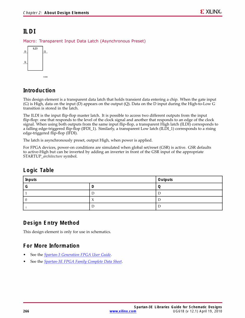
Chapter 2: About Design Elements
ILDIMacro: Transparent Input Data Latch (Asynchronous Preset)
IntroductionThis design element is a transparent data latch that holds transient data entering a chip. When the gate input(G) is High, data on the input (D) appears on the output (Q). Data on the D input during the High-to-Low Gtransition is stored in the latch.
The ILDI is the input flip-flop master latch. It is possible to access two different outputs from the inputflip-flop: one that responds to the level of the clock signal and another that responds to an edge of the clocksignal. When using both outputs from the same input flip-flop, a transparent High latch (ILDI) corresponds toa falling edge-triggered flip-flop (IFDI_1). Similarly, a transparent Low latch (ILDI_1) corresponds to a risingedge-triggered flip-flop (IFDI).
The latch is asynchronously preset, output High, when power is applied.
For FPGA devices, power-on conditions are simulated when global set/reset (GSR) is active. GSR defaultsto active-High but can be inverted by adding an inverter in front of the GSR input of the appropriateSTARTUP_architecture symbol.
Logic TableInputs Outputs
G D Q1 D D
0 X D
↓ D D
Design Entry MethodThis design element is only for use in schematics.
For More Information• See the Spartan-3 Generation FPGA User Guide.
• See the Spartan-3E FPGA Family Complete Data Sheet.
Spartan-3E Libraries Guide for Schematic Designs266 www.xilinx.com UG618 (v 12.1) April 19, 2010
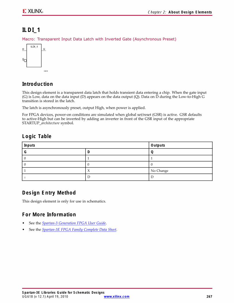
Chapter 2: About Design Elements
ILDI_1Macro: Transparent Input Data Latch with Inverted Gate (Asynchronous Preset)
IntroductionThis design element is a transparent data latch that holds transient data entering a chip. When the gate input(G) is Low, data on the data input (D) appears on the data output (Q). Data on D during the Low-to-High Gtransition is stored in the latch.
The latch is asynchronously preset, output High, when power is applied.
For FPGA devices, power-on conditions are simulated when global set/reset (GSR) is active. GSR defaultsto active-High but can be inverted by adding an inverter in front of the GSR input of the appropriateSTARTUP_architecture symbol.
Logic TableInputs Outputs
G D Q0 1 1
0 0 0
1 X No Change
↑ D D
Design Entry MethodThis design element is only for use in schematics.
For More Information• See the Spartan-3 Generation FPGA User Guide.
• See the Spartan-3E FPGA Family Complete Data Sheet.
Spartan-3E Libraries Guide for Schematic DesignsUG618 (v 12.1) April 19, 2010 www.xilinx.com 267
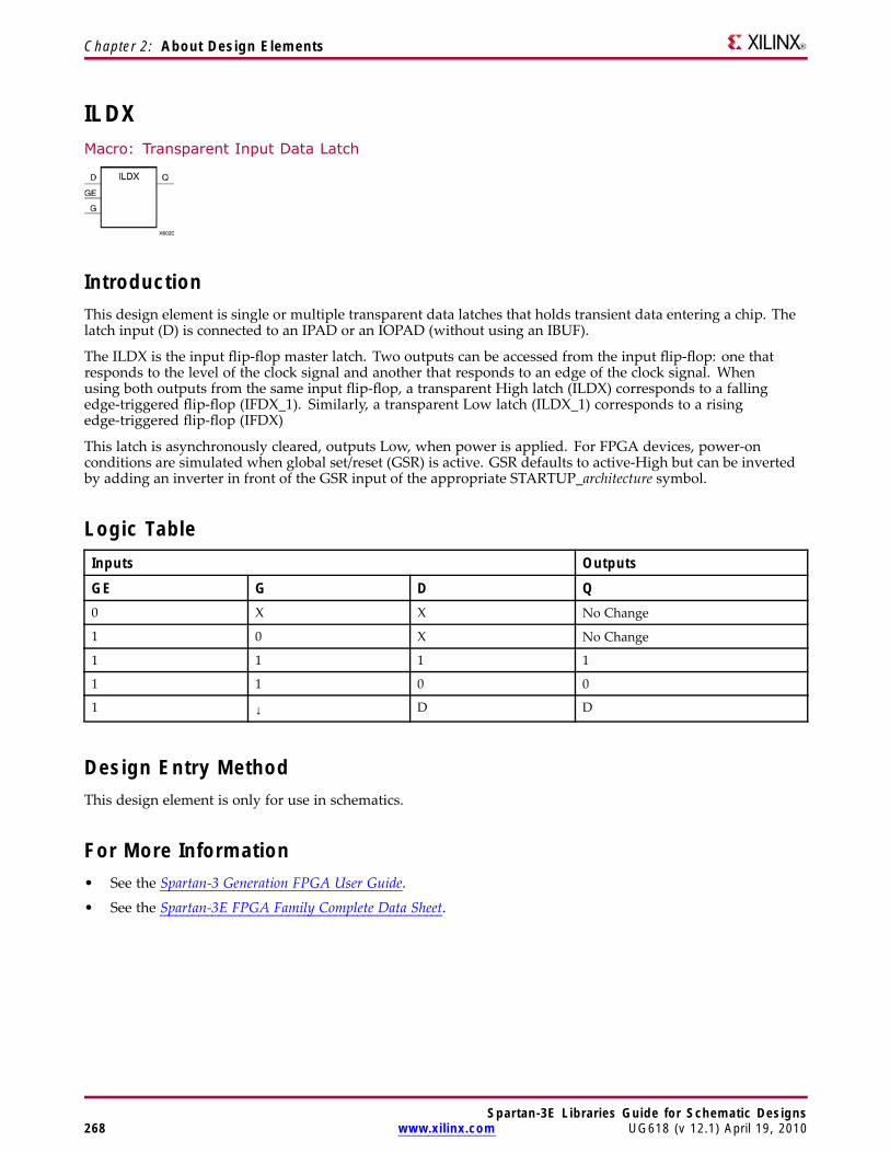
Chapter 2: About Design Elements
ILDXMacro: Transparent Input Data Latch
IntroductionThis design element is single or multiple transparent data latches that holds transient data entering a chip. Thelatch input (D) is connected to an IPAD or an IOPAD (without using an IBUF).
The ILDX is the input flip-flop master latch. Two outputs can be accessed from the input flip-flop: one thatresponds to the level of the clock signal and another that responds to an edge of the clock signal. Whenusing both outputs from the same input flip-flop, a transparent High latch (ILDX) corresponds to a fallingedge-triggered flip-flop (IFDX_1). Similarly, a transparent Low latch (ILDX_1) corresponds to a risingedge-triggered flip-flop (IFDX)
This latch is asynchronously cleared, outputs Low, when power is applied. For FPGA devices, power-onconditions are simulated when global set/reset (GSR) is active. GSR defaults to active-High but can be invertedby adding an inverter in front of the GSR input of the appropriate STARTUP_architecture symbol.
Logic TableInputs Outputs
GE G D Q0 X X No Change
1 0 X No Change
1 1 1 1
1 1 0 0
1 ↓ D D
Design Entry MethodThis design element is only for use in schematics.
For More Information• See the Spartan-3 Generation FPGA User Guide.
• See the Spartan-3E FPGA Family Complete Data Sheet.
Spartan-3E Libraries Guide for Schematic Designs268 www.xilinx.com UG618 (v 12.1) April 19, 2010
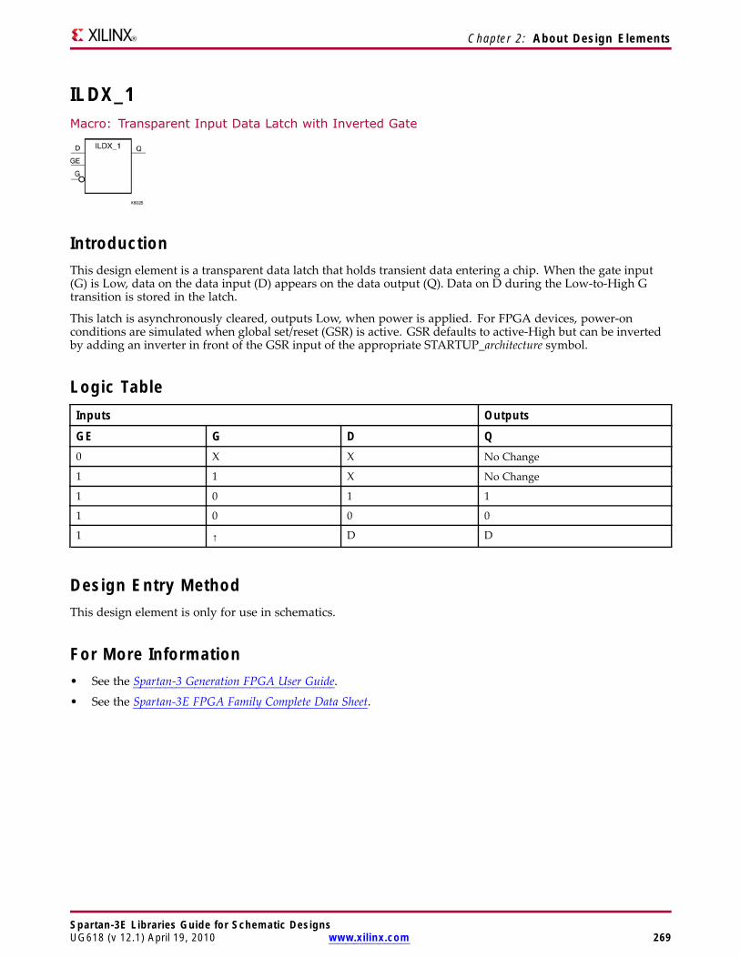
Chapter 2: About Design Elements
ILDX_1Macro: Transparent Input Data Latch with Inverted Gate
IntroductionThis design element is a transparent data latch that holds transient data entering a chip. When the gate input(G) is Low, data on the data input (D) appears on the data output (Q). Data on D during the Low-to-High Gtransition is stored in the latch.
This latch is asynchronously cleared, outputs Low, when power is applied. For FPGA devices, power-onconditions are simulated when global set/reset (GSR) is active. GSR defaults to active-High but can be invertedby adding an inverter in front of the GSR input of the appropriate STARTUP_architecture symbol.
Logic TableInputs Outputs
GE G D Q0 X X No Change
1 1 X No Change
1 0 1 1
1 0 0 0
1 ↑ D D
Design Entry MethodThis design element is only for use in schematics.
For More Information• See the Spartan-3 Generation FPGA User Guide.
• See the Spartan-3E FPGA Family Complete Data Sheet.
Spartan-3E Libraries Guide for Schematic DesignsUG618 (v 12.1) April 19, 2010 www.xilinx.com 269
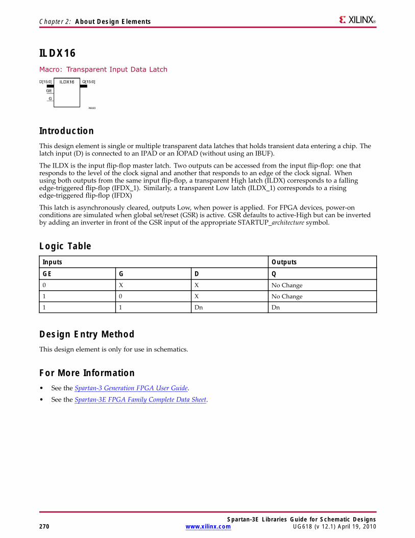
Chapter 2: About Design Elements
ILDX16Macro: Transparent Input Data Latch
IntroductionThis design element is single or multiple transparent data latches that holds transient data entering a chip. Thelatch input (D) is connected to an IPAD or an IOPAD (without using an IBUF).
The ILDX is the input flip-flop master latch. Two outputs can be accessed from the input flip-flop: one thatresponds to the level of the clock signal and another that responds to an edge of the clock signal. Whenusing both outputs from the same input flip-flop, a transparent High latch (ILDX) corresponds to a fallingedge-triggered flip-flop (IFDX_1). Similarly, a transparent Low latch (ILDX_1) corresponds to a risingedge-triggered flip-flop (IFDX)
This latch is asynchronously cleared, outputs Low, when power is applied. For FPGA devices, power-onconditions are simulated when global set/reset (GSR) is active. GSR defaults to active-High but can be invertedby adding an inverter in front of the GSR input of the appropriate STARTUP_architecture symbol.
Logic TableInputs Outputs
GE G D Q0 X X No Change
1 0 X No Change
1 1 Dn Dn
Design Entry MethodThis design element is only for use in schematics.
For More Information• See the Spartan-3 Generation FPGA User Guide.
• See the Spartan-3E FPGA Family Complete Data Sheet.
Spartan-3E Libraries Guide for Schematic Designs270 www.xilinx.com UG618 (v 12.1) April 19, 2010
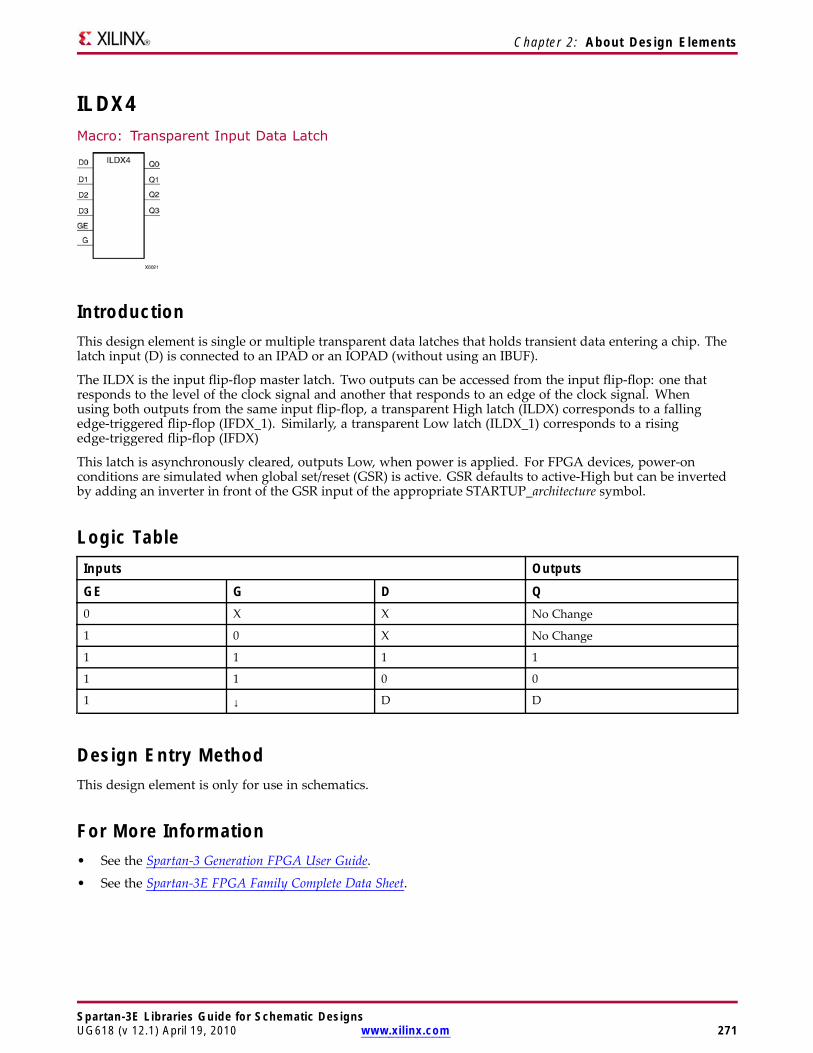
Chapter 2: About Design Elements
ILDX4Macro: Transparent Input Data Latch
IntroductionThis design element is single or multiple transparent data latches that holds transient data entering a chip. Thelatch input (D) is connected to an IPAD or an IOPAD (without using an IBUF).
The ILDX is the input flip-flop master latch. Two outputs can be accessed from the input flip-flop: one thatresponds to the level of the clock signal and another that responds to an edge of the clock signal. Whenusing both outputs from the same input flip-flop, a transparent High latch (ILDX) corresponds to a fallingedge-triggered flip-flop (IFDX_1). Similarly, a transparent Low latch (ILDX_1) corresponds to a risingedge-triggered flip-flop (IFDX)
This latch is asynchronously cleared, outputs Low, when power is applied. For FPGA devices, power-onconditions are simulated when global set/reset (GSR) is active. GSR defaults to active-High but can be invertedby adding an inverter in front of the GSR input of the appropriate STARTUP_architecture symbol.
Logic TableInputs Outputs
GE G D Q0 X X No Change
1 0 X No Change
1 1 1 1
1 1 0 0
1 ↓ D D
Design Entry MethodThis design element is only for use in schematics.
For More Information• See the Spartan-3 Generation FPGA User Guide.
• See the Spartan-3E FPGA Family Complete Data Sheet.
Spartan-3E Libraries Guide for Schematic DesignsUG618 (v 12.1) April 19, 2010 www.xilinx.com 271
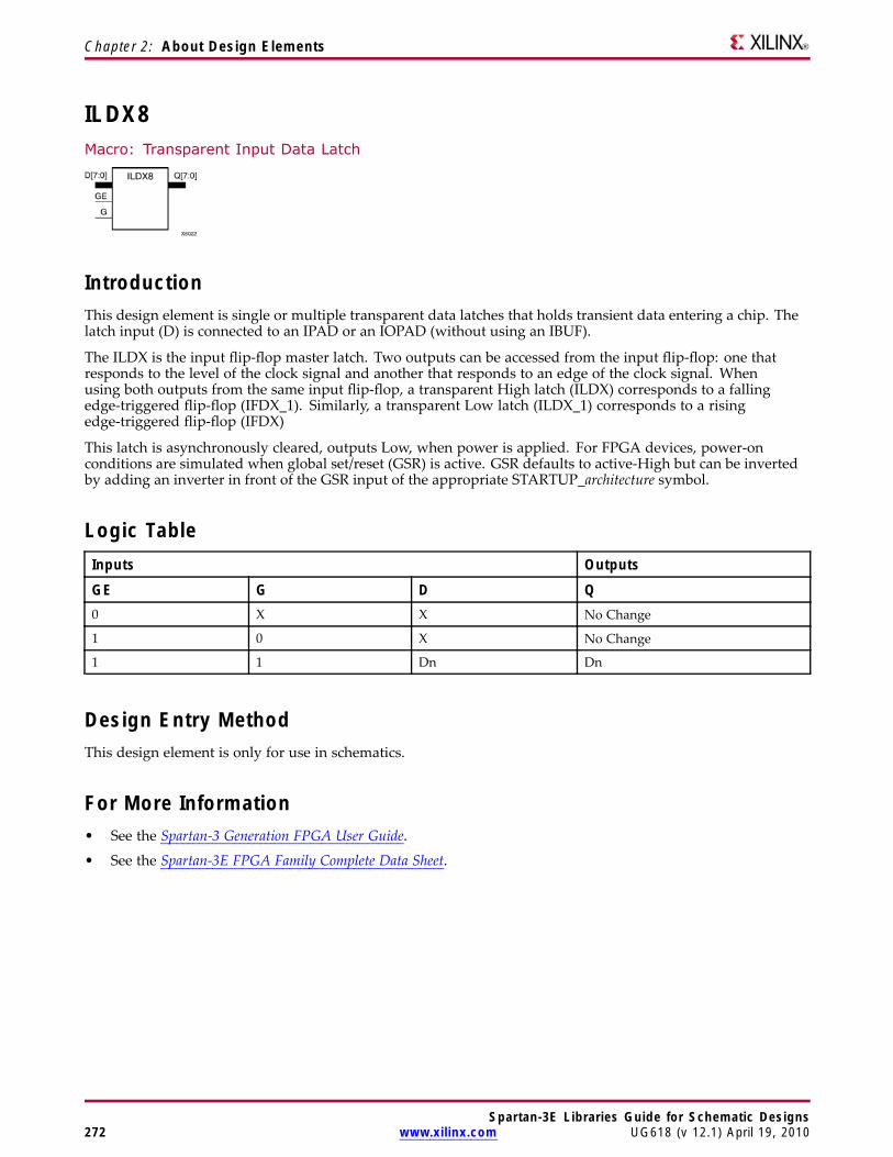
Chapter 2: About Design Elements
ILDX8Macro: Transparent Input Data Latch
IntroductionThis design element is single or multiple transparent data latches that holds transient data entering a chip. Thelatch input (D) is connected to an IPAD or an IOPAD (without using an IBUF).
The ILDX is the input flip-flop master latch. Two outputs can be accessed from the input flip-flop: one thatresponds to the level of the clock signal and another that responds to an edge of the clock signal. Whenusing both outputs from the same input flip-flop, a transparent High latch (ILDX) corresponds to a fallingedge-triggered flip-flop (IFDX_1). Similarly, a transparent Low latch (ILDX_1) corresponds to a risingedge-triggered flip-flop (IFDX)
This latch is asynchronously cleared, outputs Low, when power is applied. For FPGA devices, power-onconditions are simulated when global set/reset (GSR) is active. GSR defaults to active-High but can be invertedby adding an inverter in front of the GSR input of the appropriate STARTUP_architecture symbol.
Logic TableInputs Outputs
GE G D Q0 X X No Change
1 0 X No Change
1 1 Dn Dn
Design Entry MethodThis design element is only for use in schematics.
For More Information• See the Spartan-3 Generation FPGA User Guide.
• See the Spartan-3E FPGA Family Complete Data Sheet.
Spartan-3E Libraries Guide for Schematic Designs272 www.xilinx.com UG618 (v 12.1) April 19, 2010
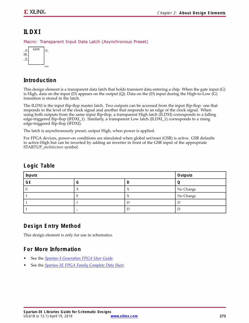
Chapter 2: About Design Elements
ILDXIMacro: Transparent Input Data Latch (Asynchronous Preset)
IntroductionThis design element is a transparent data latch that holds transient data entering a chip. When the gate input (G)is High, data on the input (D) appears on the output (Q). Data on the (D) input during the High-to-Low (G)transition is stored in the latch.
The ILDXI is the input flip-flop master latch. Two outputs can be accessed from the input flip-flop: one thatresponds to the level of the clock signal and another that responds to an edge of the clock signal. Whenusing both outputs from the same input flip-flop, a transparent High latch (ILDXI) corresponds to a fallingedge-triggered flip-flop (IFDXI_1). Similarly, a transparent Low latch (ILDXI_1) corresponds to a risingedge-triggered flip-flop (IFDXI).
The latch is asynchronously preset, output High, when power is applied.
For FPGA devices, power-on conditions are simulated when global set/reset (GSR) is active. GSR defaultsto active-High but can be inverted by adding an inverter in front of the GSR input of the appropriateSTARTUP_architecture symbol.
Logic TableInputs Outputs
GE G D Q0 X X No Change
1 0 X No Change
1 1 D D
1 ↓ D D
Design Entry MethodThis design element is only for use in schematics.
For More Information• See the Spartan-3 Generation FPGA User Guide.
• See the Spartan-3E FPGA Family Complete Data Sheet.
Spartan-3E Libraries Guide for Schematic DesignsUG618 (v 12.1) April 19, 2010 www.xilinx.com 273
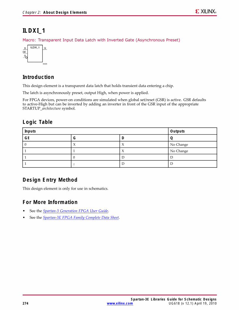
Chapter 2: About Design Elements
ILDXI_1Macro: Transparent Input Data Latch with Inverted Gate (Asynchronous Preset)
IntroductionThis design element is a transparent data latch that holds transient data entering a chip.
The latch is asynchronously preset, output High, when power is applied.
For FPGA devices, power-on conditions are simulated when global set/reset (GSR) is active. GSR defaultsto active-High but can be inverted by adding an inverter in front of the GSR input of the appropriateSTARTUP_architecture symbol.
Logic TableInputs Outputs
GE G D Q0 X X No Change
1 1 X No Change
1 0 D D
1 ↑ D D
Design Entry MethodThis design element is only for use in schematics.
For More Information• See the Spartan-3 Generation FPGA User Guide.
• See the Spartan-3E FPGA Family Complete Data Sheet.
Spartan-3E Libraries Guide for Schematic Designs274 www.xilinx.com UG618 (v 12.1) April 19, 2010
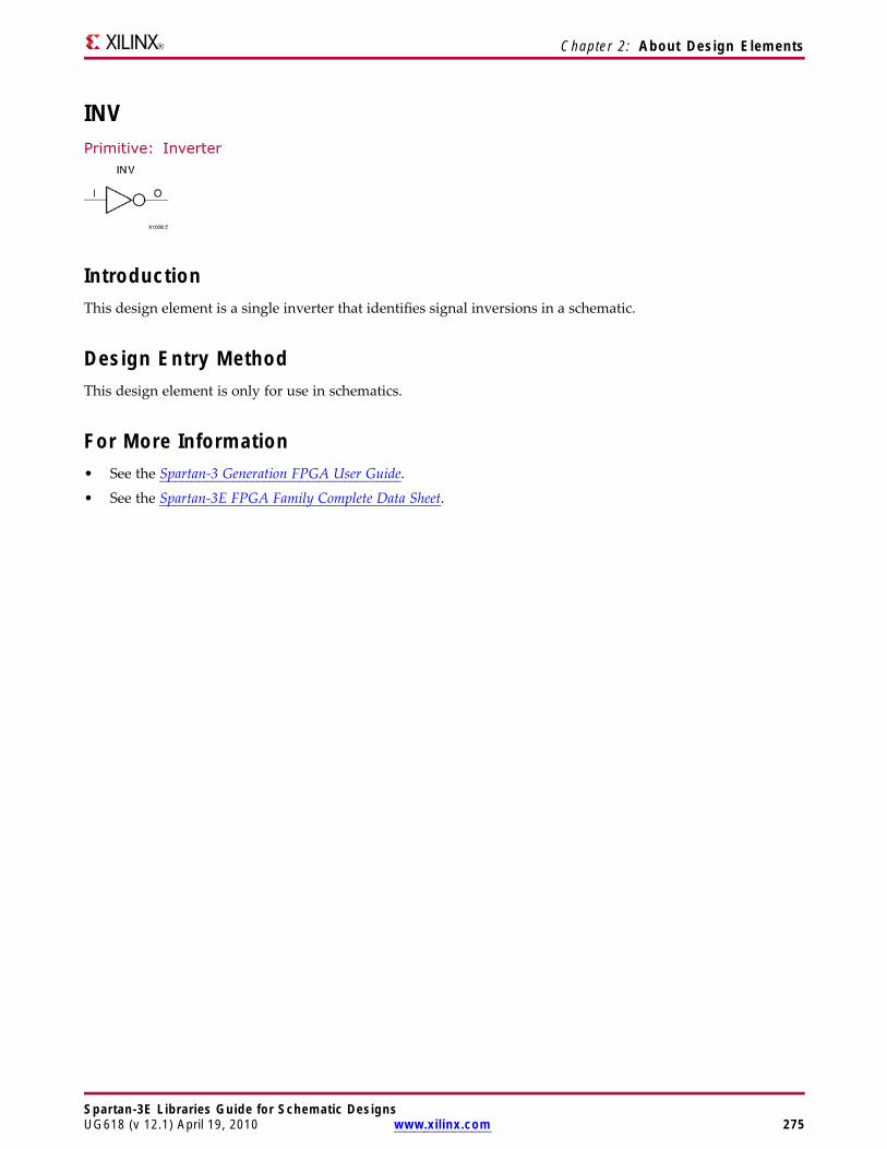
Chapter 2: About Design Elements
INVPrimitive: Inverter
IntroductionThis design element is a single inverter that identifies signal inversions in a schematic.
Design Entry MethodThis design element is only for use in schematics.
For More Information• See the Spartan-3 Generation FPGA User Guide.
• See the Spartan-3E FPGA Family Complete Data Sheet.
Spartan-3E Libraries Guide for Schematic DesignsUG618 (v 12.1) April 19, 2010 www.xilinx.com 275
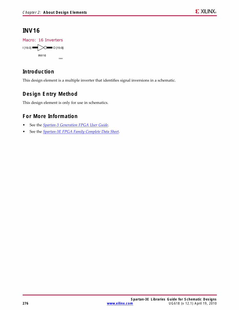
Chapter 2: About Design Elements
INV16Macro: 16 Inverters
IntroductionThis design element is a multiple inverter that identifies signal inversions in a schematic.
Design Entry MethodThis design element is only for use in schematics.
For More Information• See the Spartan-3 Generation FPGA User Guide.
• See the Spartan-3E FPGA Family Complete Data Sheet.
Spartan-3E Libraries Guide for Schematic Designs276 www.xilinx.com UG618 (v 12.1) April 19, 2010
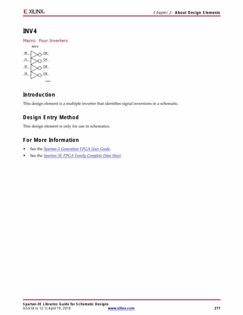
Chapter 2: About Design Elements
INV4Macro: Four Inverters
IntroductionThis design element is a multiple inverter that identifies signal inversions in a schematic.
Design Entry MethodThis design element is only for use in schematics.
For More Information• See the Spartan-3 Generation FPGA User Guide.
• See the Spartan-3E FPGA Family Complete Data Sheet.
Spartan-3E Libraries Guide for Schematic DesignsUG618 (v 12.1) April 19, 2010 www.xilinx.com 277
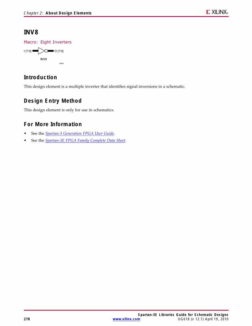
Chapter 2: About Design Elements
INV8Macro: Eight Inverters
IntroductionThis design element is a multiple inverter that identifies signal inversions in a schematic.
Design Entry MethodThis design element is only for use in schematics.
For More Information• See the Spartan-3 Generation FPGA User Guide.
• See the Spartan-3E FPGA Family Complete Data Sheet.
Spartan-3E Libraries Guide for Schematic Designs278 www.xilinx.com UG618 (v 12.1) April 19, 2010
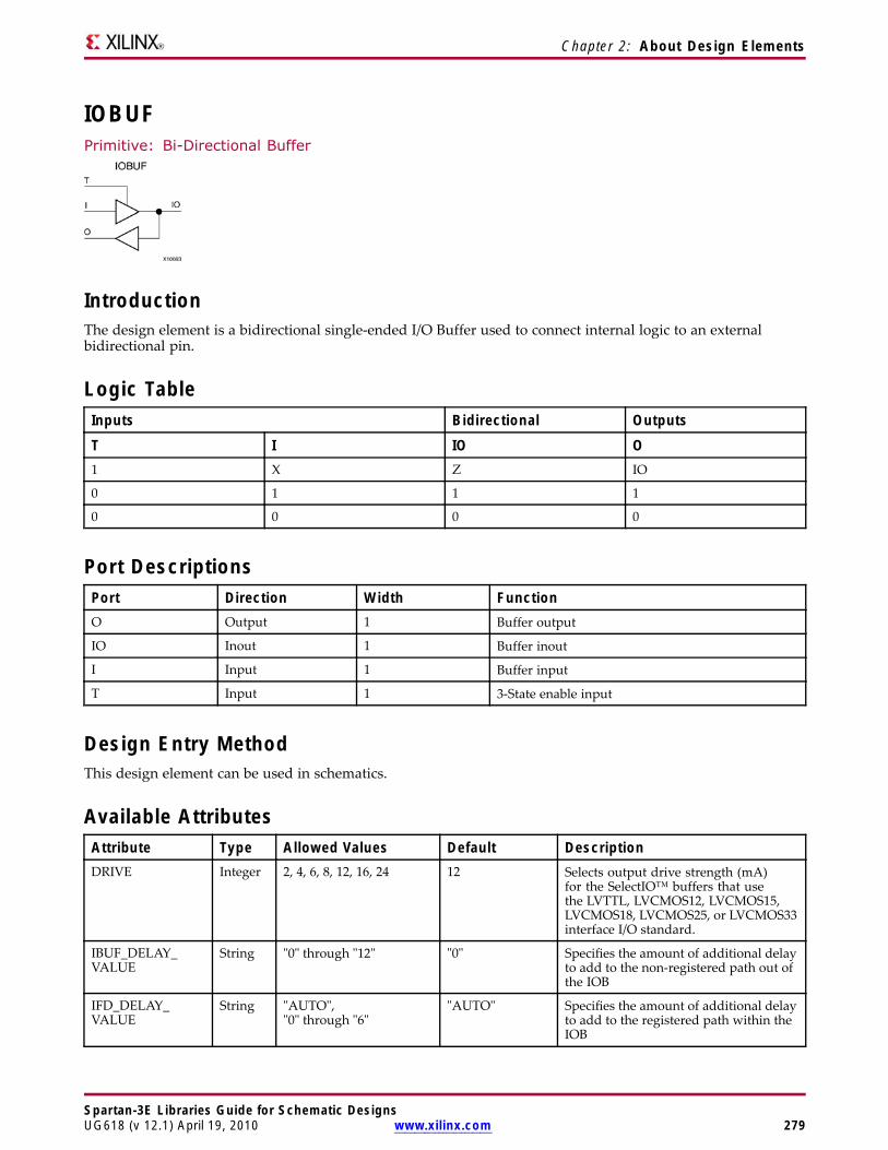
Chapter 2: About Design Elements
IOBUFPrimitive: Bi-Directional Buffer
IntroductionThe design element is a bidirectional single-ended I/O Buffer used to connect internal logic to an externalbidirectional pin.
Logic TableInputs Bidirectional Outputs
T I IO O1 X Z IO
0 1 1 1
0 0 0 0
Port DescriptionsPort Direction Width FunctionO Output 1 Buffer output
IO Inout 1 Buffer inout
I Input 1 Buffer input
T Input 1 3-State enable input
Design Entry MethodThis design element can be used in schematics.
Available AttributesAttribute Type Allowed Values Default DescriptionDRIVE Integer 2, 4, 6, 8, 12, 16, 24 12 Selects output drive strength (mA)
for the SelectIO™ buffers that usethe LVTTL, LVCMOS12, LVCMOS15,LVCMOS18, LVCMOS25, or LVCMOS33interface I/O standard.
IBUF_DELAY_VALUE
String "0" through "12" "0" Specifies the amount of additional delayto add to the non-registered path out ofthe IOB
IFD_DELAY_VALUE
String "AUTO","0" through "6"
"AUTO" Specifies the amount of additional delayto add to the registered path within theIOB
Spartan-3E Libraries Guide for Schematic DesignsUG618 (v 12.1) April 19, 2010 www.xilinx.com 279
Chapter 2: About Design Elements
Attribute Type Allowed Values Default DescriptionIOSTANDARD String See Data Sheet "DEFAULT" Assigns an I/O standard to the element.
SLEW String "SLOW", "FAST","QUIETIO"
"SLOW" Sets the output rise and fall time. See theData Sheet for recommendations of thebest setting for this attribute.
For More Information• See the Spartan-3 Generation FPGA User Guide.
• See the Spartan-3E FPGA Family Complete Data Sheet.
Spartan-3E Libraries Guide for Schematic Designs280 www.xilinx.com UG618 (v 12.1) April 19, 2010
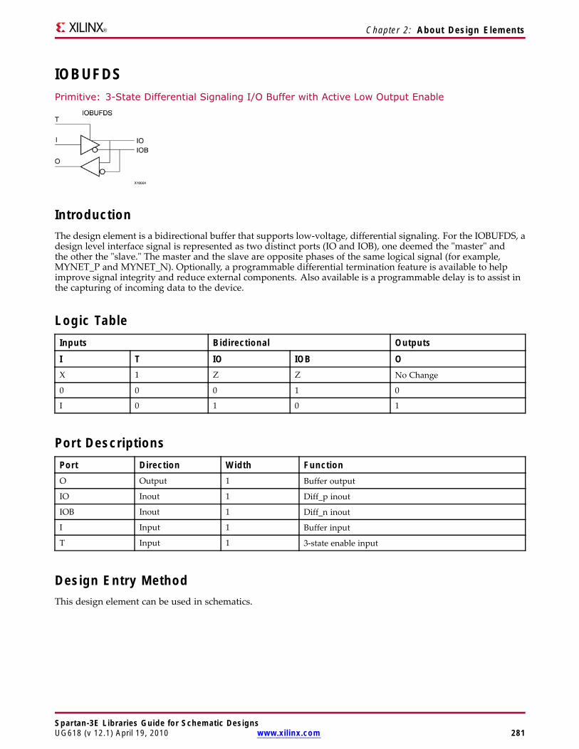
Chapter 2: About Design Elements
IOBUFDSPrimitive: 3-State Differential Signaling I/O Buffer with Active Low Output Enable
IntroductionThe design element is a bidirectional buffer that supports low-voltage, differential signaling. For the IOBUFDS, adesign level interface signal is represented as two distinct ports (IO and IOB), one deemed the "master" andthe other the "slave." The master and the slave are opposite phases of the same logical signal (for example,MYNET_P and MYNET_N). Optionally, a programmable differential termination feature is available to helpimprove signal integrity and reduce external components. Also available is a programmable delay is to assist inthe capturing of incoming data to the device.
Logic TableInputs Bidirectional Outputs
I T IO IOB OX 1 Z Z No Change
0 0 0 1 0
I 0 1 0 1
Port DescriptionsPort Direction Width FunctionO Output 1 Buffer output
IO Inout 1 Diff_p inout
IOB Inout 1 Diff_n inout
I Input 1 Buffer input
T Input 1 3-state enable input
Design Entry MethodThis design element can be used in schematics.
Spartan-3E Libraries Guide for Schematic DesignsUG618 (v 12.1) April 19, 2010 www.xilinx.com 281
Chapter 2: About Design Elements
Available AttributesAttribute Type Allowed Values Default DescriptionIBUF_DELAY_VALUE
String "0" through "12" "0" Specifies the amount of additional delayto add to the non-registered path outof the IOB
IFD_DELAY_VALUE
String "AUTO","0" through "6"
"AUTO" Specifies the amount of additional delayto add to the registered path within theIOB
IOSTANDARD String See Data Sheet "DEFAULT" Assigns an I/O standard to the element.
For More Information• See the Spartan-3 Generation FPGA User Guide.
• See the Spartan-3E FPGA Family Complete Data Sheet.
Spartan-3E Libraries Guide for Schematic Designs282 www.xilinx.com UG618 (v 12.1) April 19, 2010
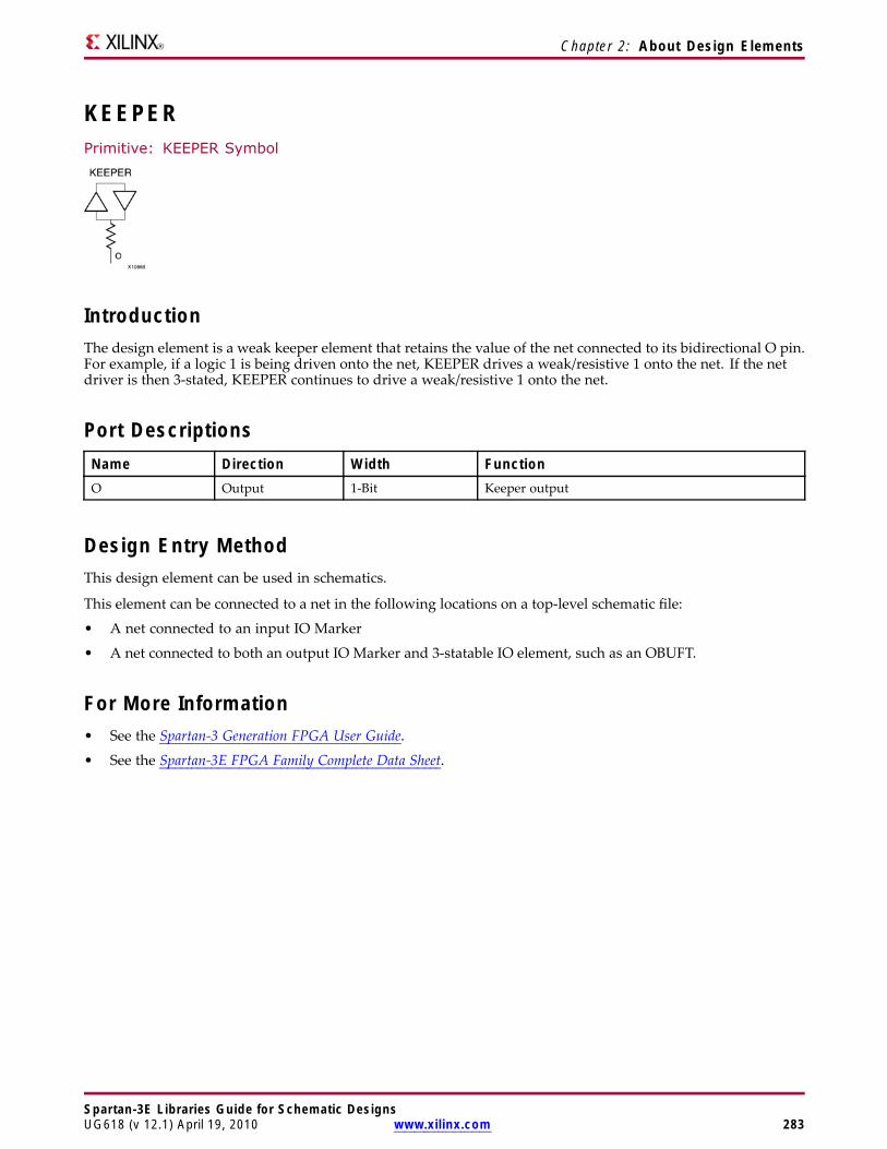
Chapter 2: About Design Elements
KEEPERPrimitive: KEEPER Symbol
IntroductionThe design element is a weak keeper element that retains the value of the net connected to its bidirectional O pin.For example, if a logic 1 is being driven onto the net, KEEPER drives a weak/resistive 1 onto the net. If the netdriver is then 3-stated, KEEPER continues to drive a weak/resistive 1 onto the net.
Port DescriptionsName Direction Width FunctionO Output 1-Bit Keeper output
Design Entry MethodThis design element can be used in schematics.
This element can be connected to a net in the following locations on a top-level schematic file:
• A net connected to an input IO Marker
• A net connected to both an output IO Marker and 3-statable IO element, such as an OBUFT.
For More Information• See the Spartan-3 Generation FPGA User Guide.
• See the Spartan-3E FPGA Family Complete Data Sheet.
Spartan-3E Libraries Guide for Schematic DesignsUG618 (v 12.1) April 19, 2010 www.xilinx.com 283
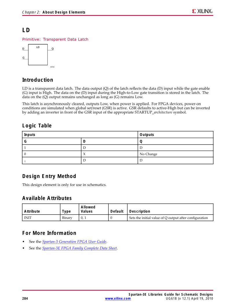
Chapter 2: About Design Elements
LDPrimitive: Transparent Data Latch
IntroductionLD is a transparent data latch. The data output (Q) of the latch reflects the data (D) input while the gate enable(G) input is High. The data on the (D) input during the High-to-Low gate transition is stored in the latch. Thedata on the (Q) output remains unchanged as long as (G) remains Low.
This latch is asynchronously cleared, outputs Low, when power is applied. For FPGA devices, power-onconditions are simulated when global set/reset (GSR) is active. GSR defaults to active-High but can be invertedby adding an inverter in front of the GSR input of the appropriate STARTUP_architecture symbol.
Logic TableInputs Outputs
G D Q1 D D
0 X No Change
↓ D D
Design Entry MethodThis design element is only for use in schematics.
Available Attributes
Attribute TypeAllowedValues Default Description
INIT Binary 0, 1 0 Sets the initial value of Q output after configuration
For More Information• See the Spartan-3 Generation FPGA User Guide.
• See the Spartan-3E FPGA Family Complete Data Sheet.
Spartan-3E Libraries Guide for Schematic Designs284 www.xilinx.com UG618 (v 12.1) April 19, 2010
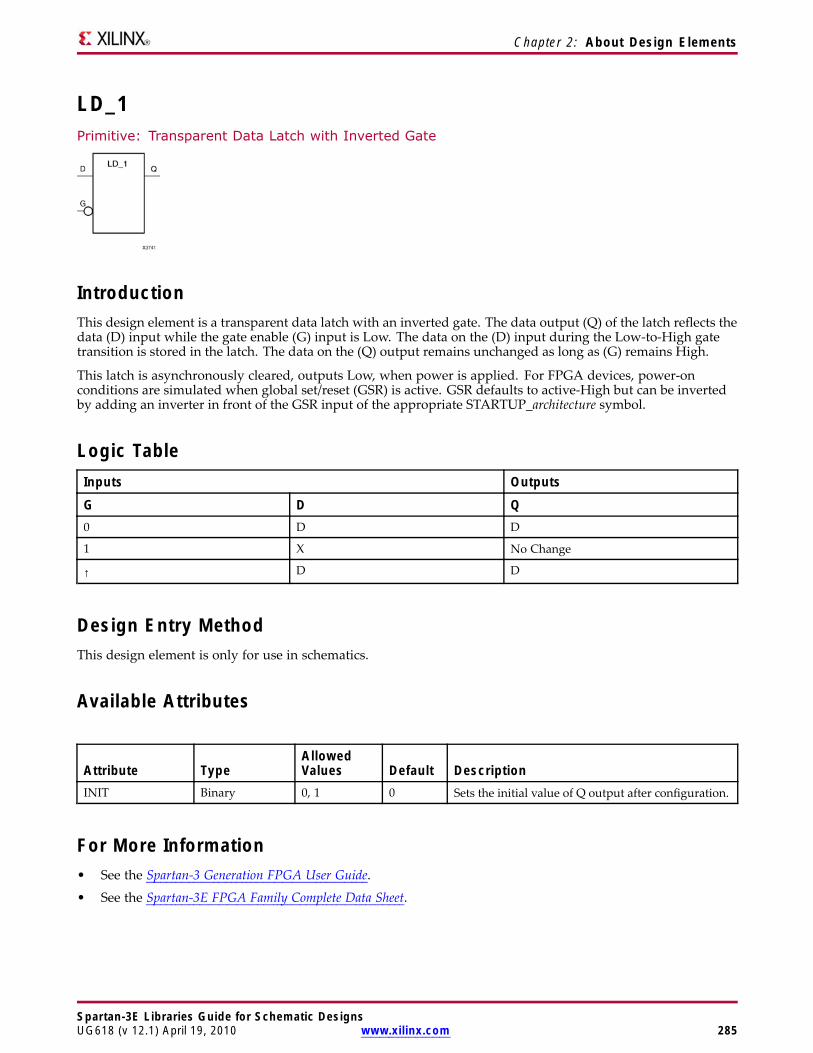
Chapter 2: About Design Elements
LD_1Primitive: Transparent Data Latch with Inverted Gate
IntroductionThis design element is a transparent data latch with an inverted gate. The data output (Q) of the latch reflects thedata (D) input while the gate enable (G) input is Low. The data on the (D) input during the Low-to-High gatetransition is stored in the latch. The data on the (Q) output remains unchanged as long as (G) remains High.
This latch is asynchronously cleared, outputs Low, when power is applied. For FPGA devices, power-onconditions are simulated when global set/reset (GSR) is active. GSR defaults to active-High but can be invertedby adding an inverter in front of the GSR input of the appropriate STARTUP_architecture symbol.
Logic TableInputs Outputs
G D Q0 D D
1 X No Change
↑ D D
Design Entry MethodThis design element is only for use in schematics.
Available Attributes
Attribute TypeAllowedValues Default Description
INIT Binary 0, 1 0 Sets the initial value of Q output after configuration.
For More Information• See the Spartan-3 Generation FPGA User Guide.
• See the Spartan-3E FPGA Family Complete Data Sheet.
Spartan-3E Libraries Guide for Schematic DesignsUG618 (v 12.1) April 19, 2010 www.xilinx.com 285
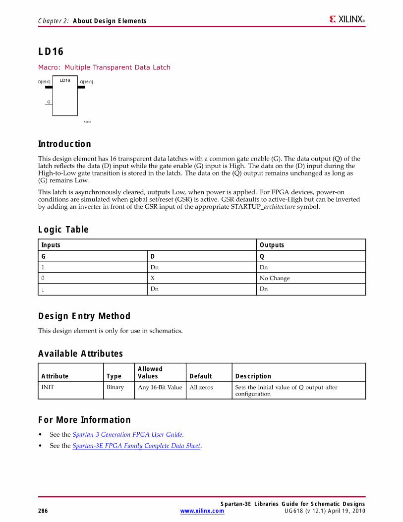
Chapter 2: About Design Elements
LD16Macro: Multiple Transparent Data Latch
IntroductionThis design element has 16 transparent data latches with a common gate enable (G). The data output (Q) of thelatch reflects the data (D) input while the gate enable (G) input is High. The data on the (D) input during theHigh-to-Low gate transition is stored in the latch. The data on the (Q) output remains unchanged as long as(G) remains Low.
This latch is asynchronously cleared, outputs Low, when power is applied. For FPGA devices, power-onconditions are simulated when global set/reset (GSR) is active. GSR defaults to active-High but can be invertedby adding an inverter in front of the GSR input of the appropriate STARTUP_architecture symbol.
Logic TableInputs Outputs
G D Q1 Dn Dn
0 X No Change
↓ Dn Dn
Design Entry MethodThis design element is only for use in schematics.
Available Attributes
Attribute TypeAllowedValues Default Description
INIT Binary Any 16-Bit Value All zeros Sets the initial value of Q output afterconfiguration
For More Information• See the Spartan-3 Generation FPGA User Guide.
• See the Spartan-3E FPGA Family Complete Data Sheet.
Spartan-3E Libraries Guide for Schematic Designs286 www.xilinx.com UG618 (v 12.1) April 19, 2010
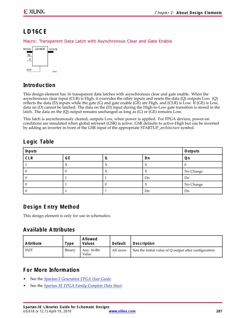
Chapter 2: About Design Elements
LD16CEMacro: Transparent Data Latch with Asynchronous Clear and Gate Enable
IntroductionThis design element has 16 transparent data latches with asynchronous clear and gate enable. When theasynchronous clear input (CLR) is High, it overrides the other inputs and resets the data (Q) outputs Low. (Q)reflects the data (D) inputs while the gate (G) and gate enable (GE) are High, and (CLR) is Low. If (GE) is Low,data on (D) cannot be latched. The data on the (D) input during the High-to-Low gate transition is stored in thelatch. The data on the (Q) output remains unchanged as long as (G) or (GE) remains Low.
This latch is asynchronously cleared, outputs Low, when power is applied. For FPGA devices, power-onconditions are simulated when global set/reset (GSR) is active. GSR defaults to active-High but can be invertedby adding an inverter in front of the GSR input of the appropriate STARTUP_architecture symbol.
Logic TableInputs Outputs
CLR GE G Dn Qn1 X X X 0
0 0 X X No Change
0 1 1 Dn Dn
0 1 0 X No Change
0 1 ? Dn Dn
Design Entry MethodThis design element is only for use in schematics.
Available Attributes
Attribute TypeAllowedValues Default Description
INIT Binary Any 16-BitValue
All zeros Sets the initial value of Q output after configuration
For More Information• See the Spartan-3 Generation FPGA User Guide.
• See the Spartan-3E FPGA Family Complete Data Sheet.
Spartan-3E Libraries Guide for Schematic DesignsUG618 (v 12.1) April 19, 2010 www.xilinx.com 287

Chapter 2: About Design Elements
LD4Macro: Multiple Transparent Data Latch
IntroductionThis design element has four transparent data latches with a common gate enable (G). The data output (Q) of thelatch reflects the data (D) input while the gate enable (G) input is High. The data on the (D) input during theHigh-to-Low gate transition is stored in the latch. The data on the (Q) output remains unchanged as long as(G) remains Low.
This latch is asynchronously cleared, outputs Low, when power is applied. For FPGA devices, power-onconditions are simulated when global set/reset (GSR) is active. GSR defaults to active-High but can be invertedby adding an inverter in front of the GSR input of the appropriate STARTUP_architecture symbol.
Logic TableInputs Outputs
G D Q1 Dn Dn
0 X No Change
↓ Dn Dn
Design Entry MethodThis design element is only for use in schematics.
Available Attributes
Attribute TypeAllowedValues Default Description
INIT Binary Any 4-Bit Value All zeros Sets the initial value of Q output after configuration
For More Information• See the Spartan-3 Generation FPGA User Guide.
• See the Spartan-3E FPGA Family Complete Data Sheet.
Spartan-3E Libraries Guide for Schematic Designs288 www.xilinx.com UG618 (v 12.1) April 19, 2010
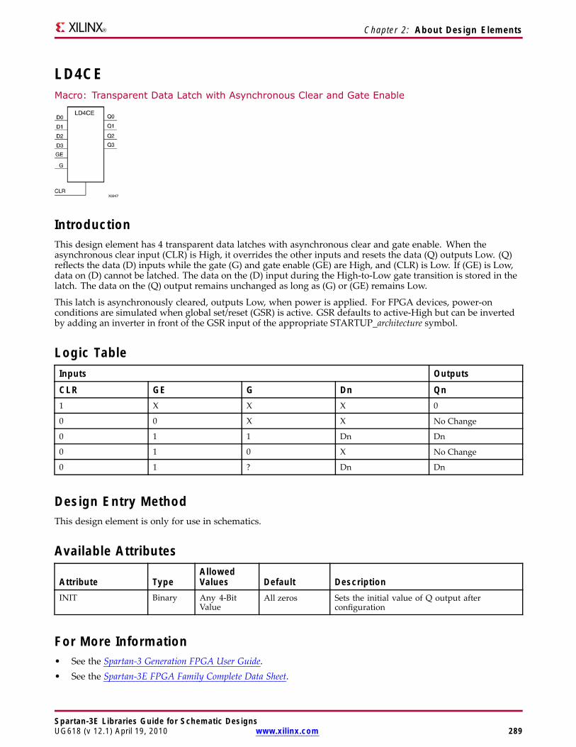
Chapter 2: About Design Elements
LD4CEMacro: Transparent Data Latch with Asynchronous Clear and Gate Enable
IntroductionThis design element has 4 transparent data latches with asynchronous clear and gate enable. When theasynchronous clear input (CLR) is High, it overrides the other inputs and resets the data (Q) outputs Low. (Q)reflects the data (D) inputs while the gate (G) and gate enable (GE) are High, and (CLR) is Low. If (GE) is Low,data on (D) cannot be latched. The data on the (D) input during the High-to-Low gate transition is stored in thelatch. The data on the (Q) output remains unchanged as long as (G) or (GE) remains Low.
This latch is asynchronously cleared, outputs Low, when power is applied. For FPGA devices, power-onconditions are simulated when global set/reset (GSR) is active. GSR defaults to active-High but can be invertedby adding an inverter in front of the GSR input of the appropriate STARTUP_architecture symbol.
Logic TableInputs Outputs
CLR GE G Dn Qn1 X X X 0
0 0 X X No Change
0 1 1 Dn Dn
0 1 0 X No Change
0 1 ? Dn Dn
Design Entry MethodThis design element is only for use in schematics.
Available Attributes
Attribute TypeAllowedValues Default Description
INIT Binary Any 4-BitValue
All zeros Sets the initial value of Q output afterconfiguration
For More Information• See the Spartan-3 Generation FPGA User Guide.• See the Spartan-3E FPGA Family Complete Data Sheet.
Spartan-3E Libraries Guide for Schematic DesignsUG618 (v 12.1) April 19, 2010 www.xilinx.com 289
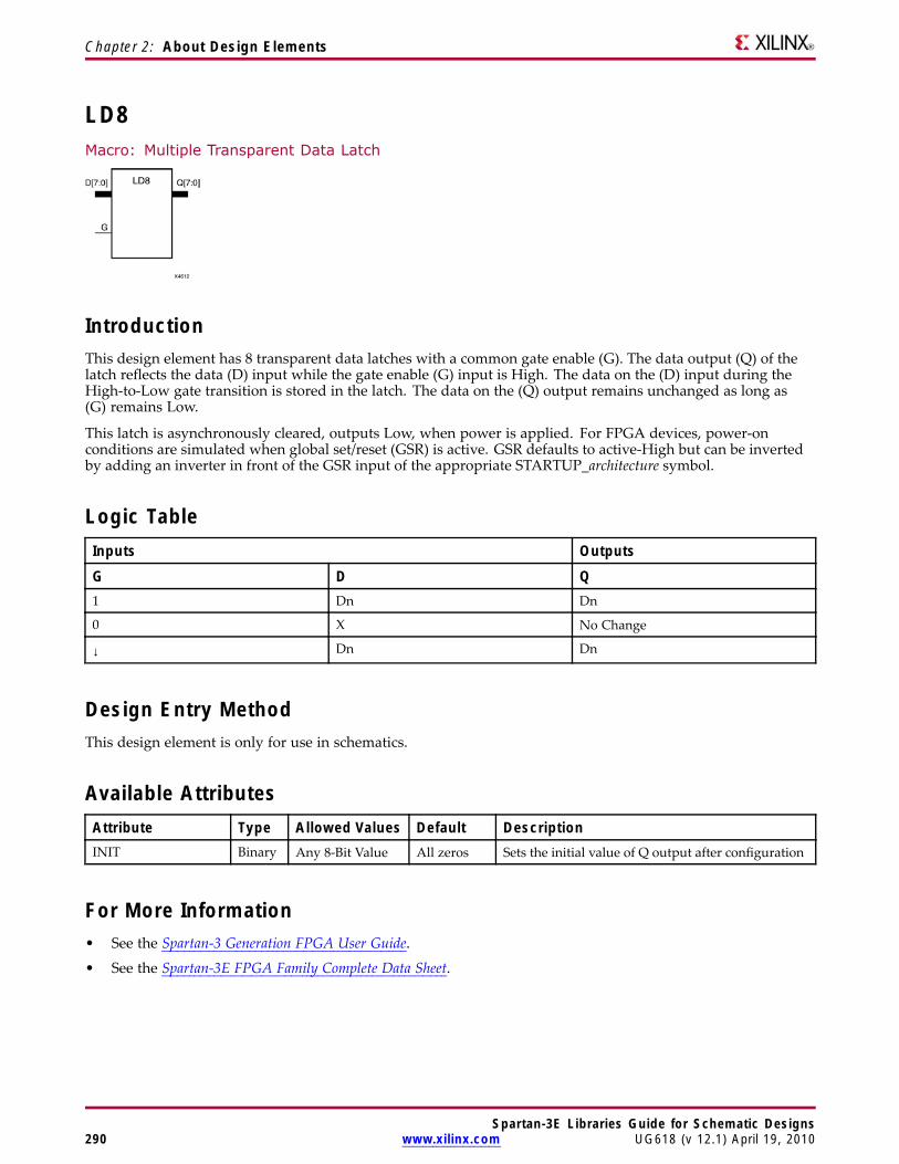
Chapter 2: About Design Elements
LD8Macro: Multiple Transparent Data Latch
IntroductionThis design element has 8 transparent data latches with a common gate enable (G). The data output (Q) of thelatch reflects the data (D) input while the gate enable (G) input is High. The data on the (D) input during theHigh-to-Low gate transition is stored in the latch. The data on the (Q) output remains unchanged as long as(G) remains Low.
This latch is asynchronously cleared, outputs Low, when power is applied. For FPGA devices, power-onconditions are simulated when global set/reset (GSR) is active. GSR defaults to active-High but can be invertedby adding an inverter in front of the GSR input of the appropriate STARTUP_architecture symbol.
Logic TableInputs Outputs
G D Q1 Dn Dn
0 X No Change
↓ Dn Dn
Design Entry MethodThis design element is only for use in schematics.
Available AttributesAttribute Type Allowed Values Default DescriptionINIT Binary Any 8-Bit Value All zeros Sets the initial value of Q output after configuration
For More Information• See the Spartan-3 Generation FPGA User Guide.
• See the Spartan-3E FPGA Family Complete Data Sheet.
Spartan-3E Libraries Guide for Schematic Designs290 www.xilinx.com UG618 (v 12.1) April 19, 2010
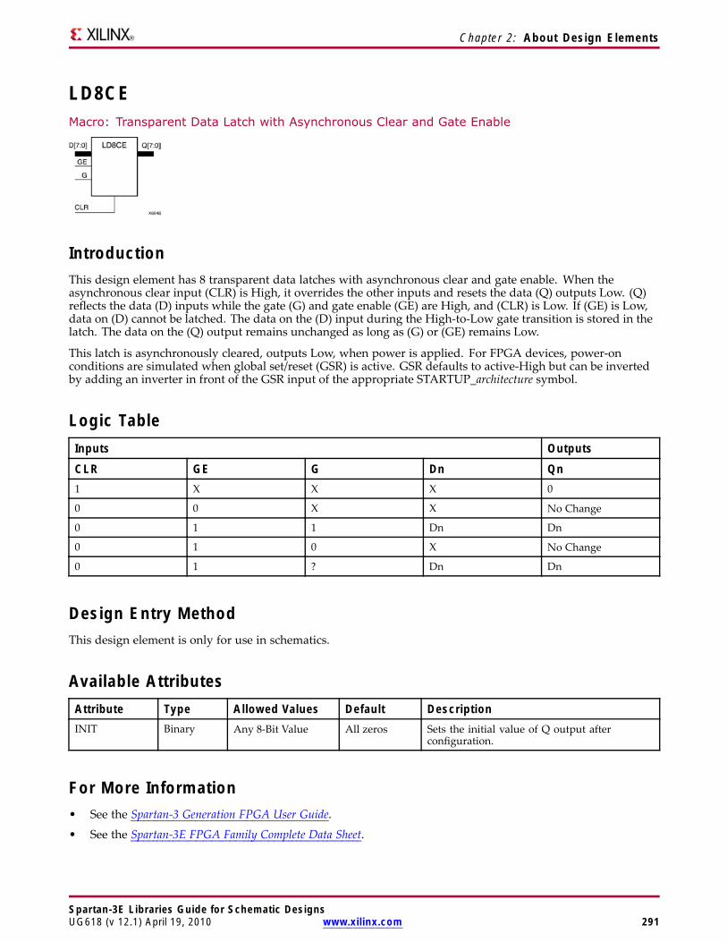
Chapter 2: About Design Elements
LD8CEMacro: Transparent Data Latch with Asynchronous Clear and Gate Enable
IntroductionThis design element has 8 transparent data latches with asynchronous clear and gate enable. When theasynchronous clear input (CLR) is High, it overrides the other inputs and resets the data (Q) outputs Low. (Q)reflects the data (D) inputs while the gate (G) and gate enable (GE) are High, and (CLR) is Low. If (GE) is Low,data on (D) cannot be latched. The data on the (D) input during the High-to-Low gate transition is stored in thelatch. The data on the (Q) output remains unchanged as long as (G) or (GE) remains Low.
This latch is asynchronously cleared, outputs Low, when power is applied. For FPGA devices, power-onconditions are simulated when global set/reset (GSR) is active. GSR defaults to active-High but can be invertedby adding an inverter in front of the GSR input of the appropriate STARTUP_architecture symbol.
Logic TableInputs Outputs
CLR GE G Dn Qn1 X X X 0
0 0 X X No Change
0 1 1 Dn Dn
0 1 0 X No Change
0 1 ? Dn Dn
Design Entry MethodThis design element is only for use in schematics.
Available AttributesAttribute Type Allowed Values Default DescriptionINIT Binary Any 8-Bit Value All zeros Sets the initial value of Q output after
configuration.
For More Information• See the Spartan-3 Generation FPGA User Guide.
• See the Spartan-3E FPGA Family Complete Data Sheet.
Spartan-3E Libraries Guide for Schematic DesignsUG618 (v 12.1) April 19, 2010 www.xilinx.com 291
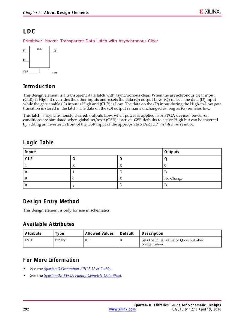
Chapter 2: About Design Elements
LDCPrimitive: Macro: Transparent Data Latch with Asynchronous Clear
IntroductionThis design element is a transparent data latch with asynchronous clear. When the asynchronous clear input(CLR) is High, it overrides the other inputs and resets the data (Q) output Low. (Q) reflects the data (D) inputwhile the gate enable (G) input is High and (CLR) is Low. The data on the (D) input during the High-to-Low gatetransition is stored in the latch. The data on the (Q) output remains unchanged as long as (G) remains low.
This latch is asynchronously cleared, outputs Low, when power is applied. For FPGA devices, power-onconditions are simulated when global set/reset (GSR) is active. GSR defaults to active-High but can be invertedby adding an inverter in front of the GSR input of the appropriate STARTUP_architecture symbol.
Logic TableInputs Outputs
CLR G D Q1 X X 0
0 1 D D
0 0 X No Change
0 ↓ D D
Design Entry MethodThis design element is only for use in schematics.
Available AttributesAttribute Type Allowed Values Default DescriptionINIT Binary 0, 1 0 Sets the initial value of Q output after
configuration.
For More Information• See the Spartan-3 Generation FPGA User Guide.
• See the Spartan-3E FPGA Family Complete Data Sheet.
Spartan-3E Libraries Guide for Schematic Designs292 www.xilinx.com UG618 (v 12.1) April 19, 2010

Chapter 2: About Design Elements
LDC_1Primitive: Transparent Data Latch with Asynchronous Clear and Inverted Gate
IntroductionThis design element is a transparent data latch with asynchronous clear and inverted gate. When theasynchronous clear input (CLR) is High, it overrides the other inputs (D and G) and resets the data (Q) outputLow. (Q) reflects the data (D) input while the gate enable (G) input and CLR are Low. The data on the (D) inputduring the Low-to-High gate transition is stored in the latch. The data on the (Q) output remains unchanged aslong as (G) remains High.
This latch is asynchronously cleared, outputs Low, when power is applied. For FPGA devices, power-onconditions are simulated when global set/reset (GSR) is active. GSR defaults to active-High but can be invertedby adding an inverter in front of the GSR input of the appropriate STARTUP_architecture symbol.
Logic TableInputs Outputs
CLR G D Q1 X X 0
0 0 D D
0 1 X No Change
0 ↑ D D
Design Entry MethodThis design element is only for use in schematics.
Available AttributesAttribute Type Allowed Values Default DescriptionINIT Binary 0, 1 0 Sets the initial value of Q output after configuration.
For More Information• See the Spartan-3 Generation FPGA User Guide.
• See the Spartan-3E FPGA Family Complete Data Sheet.
Spartan-3E Libraries Guide for Schematic DesignsUG618 (v 12.1) April 19, 2010 www.xilinx.com 293
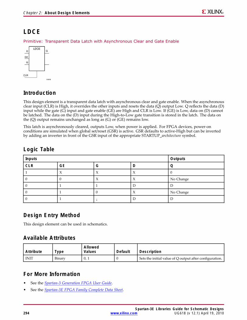
Chapter 2: About Design Elements
LDCEPrimitive: Transparent Data Latch with Asynchronous Clear and Gate Enable
IntroductionThis design element is a transparent data latch with asynchronous clear and gate enable. When the asynchronousclear input (CLR) is High, it overrides the other inputs and resets the data (Q) output Low. Q reflects the data (D)input while the gate (G) input and gate enable (GE) are High and CLR is Low. If (GE) is Low, data on (D) cannotbe latched. The data on the (D) input during the High-to-Low gate transition is stored in the latch. The data onthe (Q) output remains unchanged as long as (G) or (GE) remains low.
This latch is asynchronously cleared, outputs Low, when power is applied. For FPGA devices, power-onconditions are simulated when global set/reset (GSR) is active. GSR defaults to active-High but can be invertedby adding an inverter in front of the GSR input of the appropriate STARTUP_architecture symbol.
Logic TableInputs Outputs
CLR GE G D Q1 X X X 0
0 0 X X No Change
0 1 1 D D
0 1 0 X No Change
0 1 ↓ D D
Design Entry MethodThis design element can be used in schematics.
Available Attributes
Attribute TypeAllowedValues Default Description
INIT Binary 0, 1 0 Sets the initial value of Q output after configuration.
For More Information• See the Spartan-3 Generation FPGA User Guide.
• See the Spartan-3E FPGA Family Complete Data Sheet.
Spartan-3E Libraries Guide for Schematic Designs294 www.xilinx.com UG618 (v 12.1) April 19, 2010
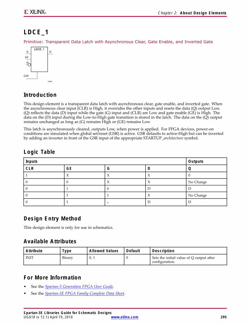
Chapter 2: About Design Elements
LDCE_1Primitive: Transparent Data Latch with Asynchronous Clear, Gate Enable, and Inverted Gate
IntroductionThis design element is a transparent data latch with asynchronous clear, gate enable, and inverted gate. Whenthe asynchronous clear input (CLR) is High, it overrides the other inputs and resets the data (Q) output Low.(Q) reflects the data (D) input while the gate (G) input and (CLR) are Low and gate enable (GE) is High. Thedata on the (D) input during the Low-to-High gate transition is stored in the latch. The data on the (Q) outputremains unchanged as long as (G) remains High or (GE) remains Low
This latch is asynchronously cleared, outputs Low, when power is applied. For FPGA devices, power-onconditions are simulated when global set/reset (GSR) is active. GSR defaults to active-High but can be invertedby adding an inverter in front of the GSR input of the appropriate STARTUP_architecture symbol.
Logic TableInputs Outputs
CLR GE G D Q1 X X X 0
0 0 X X No Change
0 1 0 D D
0 1 1 X No Change
0 1 ↑ D D
Design Entry MethodThis design element is only for use in schematics.
Available AttributesAttribute Type Allowed Values Default DescriptionINIT Binary 0, 1 0 Sets the initial value of Q output after
configuration.
For More Information• See the Spartan-3 Generation FPGA User Guide.• See the Spartan-3E FPGA Family Complete Data Sheet.
Spartan-3E Libraries Guide for Schematic DesignsUG618 (v 12.1) April 19, 2010 www.xilinx.com 295
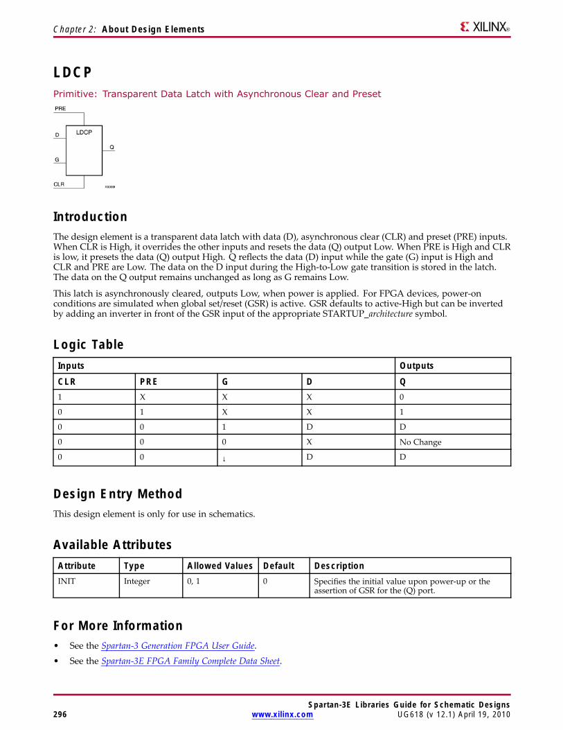
Chapter 2: About Design Elements
LDCPPrimitive: Transparent Data Latch with Asynchronous Clear and Preset
IntroductionThe design element is a transparent data latch with data (D), asynchronous clear (CLR) and preset (PRE) inputs.When CLR is High, it overrides the other inputs and resets the data (Q) output Low. When PRE is High and CLRis low, it presets the data (Q) output High. Q reflects the data (D) input while the gate (G) input is High andCLR and PRE are Low. The data on the D input during the High-to-Low gate transition is stored in the latch.The data on the Q output remains unchanged as long as G remains Low.
This latch is asynchronously cleared, outputs Low, when power is applied. For FPGA devices, power-onconditions are simulated when global set/reset (GSR) is active. GSR defaults to active-High but can be invertedby adding an inverter in front of the GSR input of the appropriate STARTUP_architecture symbol.
Logic TableInputs Outputs
CLR PRE G D Q1 X X X 0
0 1 X X 1
0 0 1 D D
0 0 0 X No Change
0 0 ↓ D D
Design Entry MethodThis design element is only for use in schematics.
Available AttributesAttribute Type Allowed Values Default DescriptionINIT Integer 0, 1 0 Specifies the initial value upon power-up or the
assertion of GSR for the (Q) port.
For More Information• See the Spartan-3 Generation FPGA User Guide.• See the Spartan-3E FPGA Family Complete Data Sheet.
Spartan-3E Libraries Guide for Schematic Designs296 www.xilinx.com UG618 (v 12.1) April 19, 2010
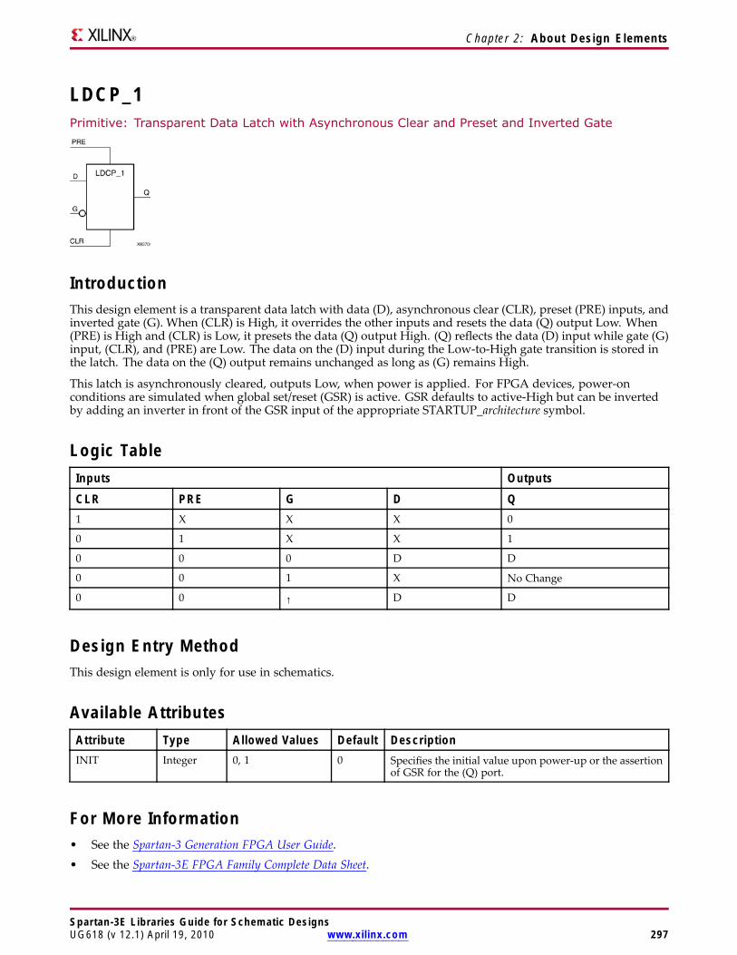
Chapter 2: About Design Elements
LDCP_1Primitive: Transparent Data Latch with Asynchronous Clear and Preset and Inverted Gate
IntroductionThis design element is a transparent data latch with data (D), asynchronous clear (CLR), preset (PRE) inputs, andinverted gate (G). When (CLR) is High, it overrides the other inputs and resets the data (Q) output Low. When(PRE) is High and (CLR) is Low, it presets the data (Q) output High. (Q) reflects the data (D) input while gate (G)input, (CLR), and (PRE) are Low. The data on the (D) input during the Low-to-High gate transition is stored inthe latch. The data on the (Q) output remains unchanged as long as (G) remains High.
This latch is asynchronously cleared, outputs Low, when power is applied. For FPGA devices, power-onconditions are simulated when global set/reset (GSR) is active. GSR defaults to active-High but can be invertedby adding an inverter in front of the GSR input of the appropriate STARTUP_architecture symbol.
Logic TableInputs Outputs
CLR PRE G D Q1 X X X 0
0 1 X X 1
0 0 0 D D
0 0 1 X No Change
0 0 ↑ D D
Design Entry MethodThis design element is only for use in schematics.
Available AttributesAttribute Type Allowed Values Default DescriptionINIT Integer 0, 1 0 Specifies the initial value upon power-up or the assertion
of GSR for the (Q) port.
For More Information• See the Spartan-3 Generation FPGA User Guide.• See the Spartan-3E FPGA Family Complete Data Sheet.
Spartan-3E Libraries Guide for Schematic DesignsUG618 (v 12.1) April 19, 2010 www.xilinx.com 297
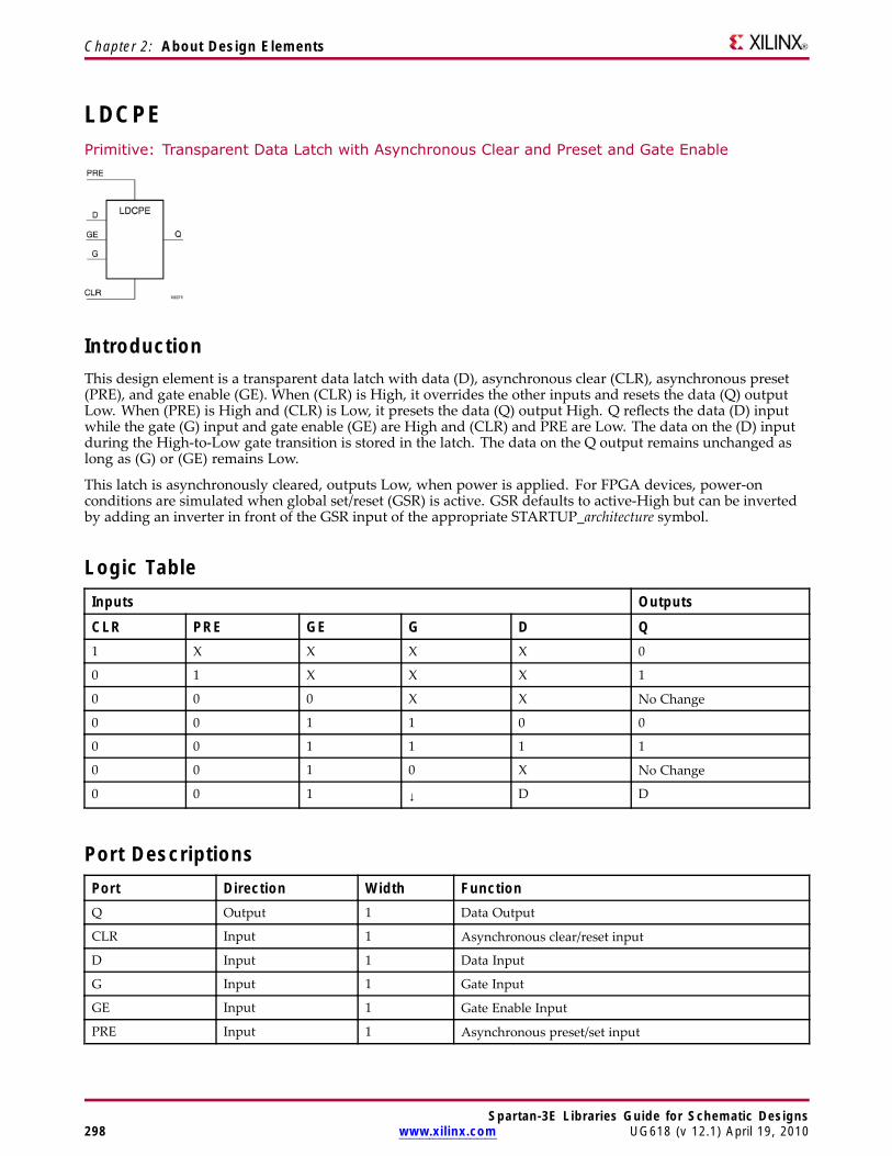
Chapter 2: About Design Elements
LDCPEPrimitive: Transparent Data Latch with Asynchronous Clear and Preset and Gate Enable
IntroductionThis design element is a transparent data latch with data (D), asynchronous clear (CLR), asynchronous preset(PRE), and gate enable (GE). When (CLR) is High, it overrides the other inputs and resets the data (Q) outputLow. When (PRE) is High and (CLR) is Low, it presets the data (Q) output High. Q reflects the data (D) inputwhile the gate (G) input and gate enable (GE) are High and (CLR) and PRE are Low. The data on the (D) inputduring the High-to-Low gate transition is stored in the latch. The data on the Q output remains unchanged aslong as (G) or (GE) remains Low.
This latch is asynchronously cleared, outputs Low, when power is applied. For FPGA devices, power-onconditions are simulated when global set/reset (GSR) is active. GSR defaults to active-High but can be invertedby adding an inverter in front of the GSR input of the appropriate STARTUP_architecture symbol.
Logic TableInputs Outputs
CLR PRE GE G D Q1 X X X X 0
0 1 X X X 1
0 0 0 X X No Change
0 0 1 1 0 0
0 0 1 1 1 1
0 0 1 0 X No Change
0 0 1 ↓ D D
Port DescriptionsPort Direction Width FunctionQ Output 1 Data Output
CLR Input 1 Asynchronous clear/reset input
D Input 1 Data Input
G Input 1 Gate Input
GE Input 1 Gate Enable Input
PRE Input 1 Asynchronous preset/set input
Spartan-3E Libraries Guide for Schematic Designs298 www.xilinx.com UG618 (v 12.1) April 19, 2010
Chapter 2: About Design Elements
Design Entry MethodThis design element can be used in schematics.
Available AttributesAttribute Type Allowed Values Default DescriptionINIT Integer 0, 1 0 Sets the initial value of Q output after configuration.
For More Information• See the Spartan-3 Generation FPGA User Guide.
• See the Spartan-3E FPGA Family Complete Data Sheet.
Spartan-3E Libraries Guide for Schematic DesignsUG618 (v 12.1) April 19, 2010 www.xilinx.com 299
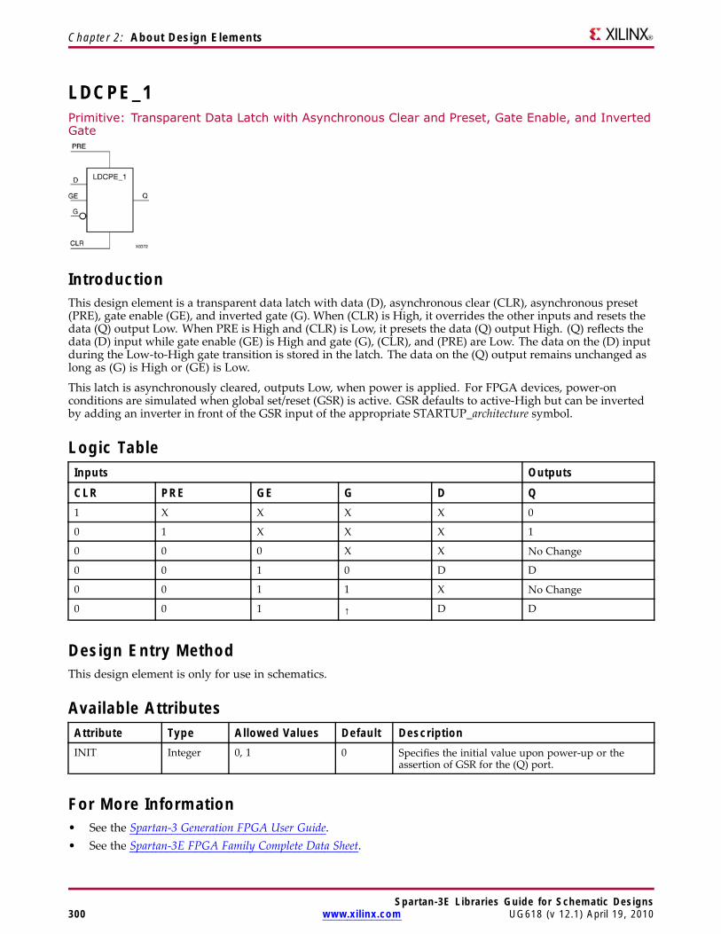
Chapter 2: About Design Elements
LDCPE_1Primitive: Transparent Data Latch with Asynchronous Clear and Preset, Gate Enable, and InvertedGate
IntroductionThis design element is a transparent data latch with data (D), asynchronous clear (CLR), asynchronous preset(PRE), gate enable (GE), and inverted gate (G). When (CLR) is High, it overrides the other inputs and resets thedata (Q) output Low. When PRE is High and (CLR) is Low, it presets the data (Q) output High. (Q) reflects thedata (D) input while gate enable (GE) is High and gate (G), (CLR), and (PRE) are Low. The data on the (D) inputduring the Low-to-High gate transition is stored in the latch. The data on the (Q) output remains unchanged aslong as (G) is High or (GE) is Low.
This latch is asynchronously cleared, outputs Low, when power is applied. For FPGA devices, power-onconditions are simulated when global set/reset (GSR) is active. GSR defaults to active-High but can be invertedby adding an inverter in front of the GSR input of the appropriate STARTUP_architecture symbol.
Logic TableInputs Outputs
CLR PRE GE G D Q1 X X X X 0
0 1 X X X 1
0 0 0 X X No Change
0 0 1 0 D D
0 0 1 1 X No Change
0 0 1 ↑ D D
Design Entry MethodThis design element is only for use in schematics.
Available AttributesAttribute Type Allowed Values Default DescriptionINIT Integer 0, 1 0 Specifies the initial value upon power-up or the
assertion of GSR for the (Q) port.
For More Information• See the Spartan-3 Generation FPGA User Guide.• See the Spartan-3E FPGA Family Complete Data Sheet.
Spartan-3E Libraries Guide for Schematic Designs300 www.xilinx.com UG618 (v 12.1) April 19, 2010
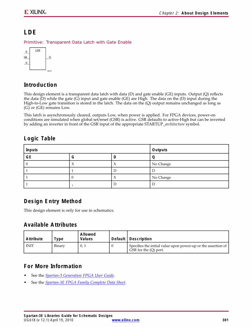
Chapter 2: About Design Elements
LDEPrimitive: Transparent Data Latch with Gate Enable
IntroductionThis design element is a transparent data latch with data (D) and gate enable (GE) inputs. Output (Q) reflectsthe data (D) while the gate (G) input and gate enable (GE) are High. The data on the (D) input during theHigh-to-Low gate transition is stored in the latch. The data on the (Q) output remains unchanged as long as(G) or (GE) remains Low.
This latch is asynchronously cleared, outputs Low, when power is applied. For FPGA devices, power-onconditions are simulated when global set/reset (GSR) is active. GSR defaults to active-High but can be invertedby adding an inverter in front of the GSR input of the appropriate STARTUP_architecture symbol.
Logic Table
Inputs Outputs
GE G D Q0 X X No Change
1 1 D D
1 0 X No Change
1 ↓ D D
Design Entry MethodThis design element is only for use in schematics.
Available Attributes
Attribute TypeAllowedValues Default Description
INIT Binary 0, 1 0 Specifies the initial value upon power-up or the assertion ofGSR for the (Q) port.
For More Information• See the Spartan-3 Generation FPGA User Guide.
• See the Spartan-3E FPGA Family Complete Data Sheet.
Spartan-3E Libraries Guide for Schematic DesignsUG618 (v 12.1) April 19, 2010 www.xilinx.com 301
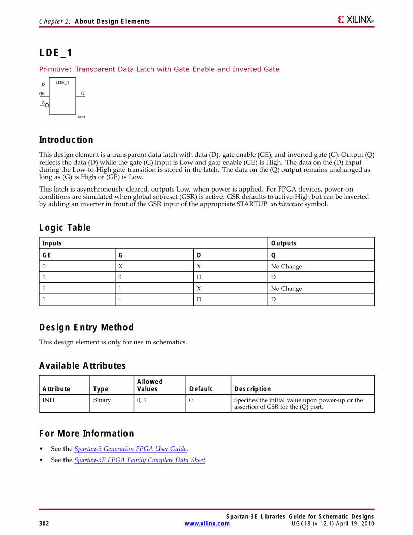
Chapter 2: About Design Elements
LDE_1Primitive: Transparent Data Latch with Gate Enable and Inverted Gate
IntroductionThis design element is a transparent data latch with data (D), gate enable (GE), and inverted gate (G). Output (Q)reflects the data (D) while the gate (G) input is Low and gate enable (GE) is High. The data on the (D) inputduring the Low-to-High gate transition is stored in the latch. The data on the (Q) output remains unchanged aslong as (G) is High or (GE) is Low.
This latch is asynchronously cleared, outputs Low, when power is applied. For FPGA devices, power-onconditions are simulated when global set/reset (GSR) is active. GSR defaults to active-High but can be invertedby adding an inverter in front of the GSR input of the appropriate STARTUP_architecture symbol.
Logic TableInputs Outputs
GE G D Q0 X X No Change
1 0 D D
1 1 X No Change
1 ↑ D D
Design Entry MethodThis design element is only for use in schematics.
Available Attributes
Attribute TypeAllowedValues Default Description
INIT Binary 0, 1 0 Specifies the initial value upon power-up or theassertion of GSR for the (Q) port.
For More Information• See the Spartan-3 Generation FPGA User Guide.
• See the Spartan-3E FPGA Family Complete Data Sheet.
Spartan-3E Libraries Guide for Schematic Designs302 www.xilinx.com UG618 (v 12.1) April 19, 2010
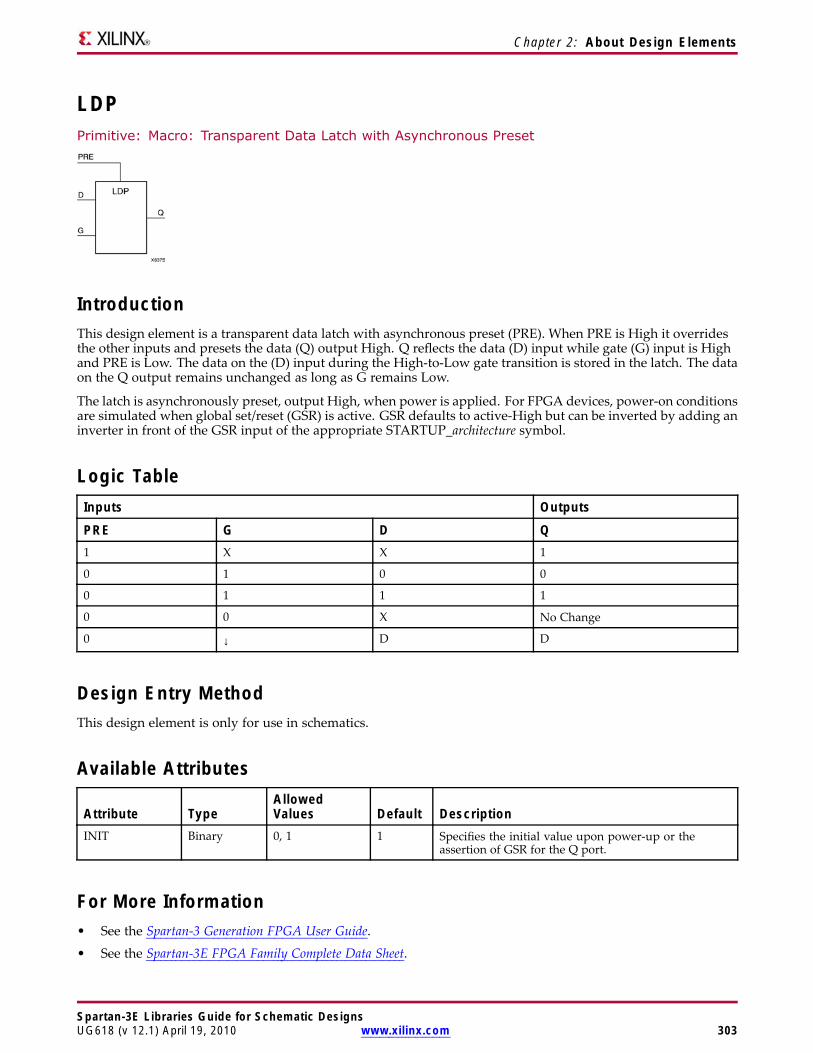
Chapter 2: About Design Elements
LDPPrimitive: Macro: Transparent Data Latch with Asynchronous Preset
IntroductionThis design element is a transparent data latch with asynchronous preset (PRE). When PRE is High it overridesthe other inputs and presets the data (Q) output High. Q reflects the data (D) input while gate (G) input is Highand PRE is Low. The data on the (D) input during the High-to-Low gate transition is stored in the latch. The dataon the Q output remains unchanged as long as G remains Low.
The latch is asynchronously preset, output High, when power is applied. For FPGA devices, power-on conditionsare simulated when global set/reset (GSR) is active. GSR defaults to active-High but can be inverted by adding aninverter in front of the GSR input of the appropriate STARTUP_architecture symbol.
Logic TableInputs Outputs
PRE G D Q1 X X 1
0 1 0 0
0 1 1 1
0 0 X No Change
0 ↓ D D
Design Entry MethodThis design element is only for use in schematics.
Available Attributes
Attribute TypeAllowedValues Default Description
INIT Binary 0, 1 1 Specifies the initial value upon power-up or theassertion of GSR for the Q port.
For More Information• See the Spartan-3 Generation FPGA User Guide.
• See the Spartan-3E FPGA Family Complete Data Sheet.
Spartan-3E Libraries Guide for Schematic DesignsUG618 (v 12.1) April 19, 2010 www.xilinx.com 303
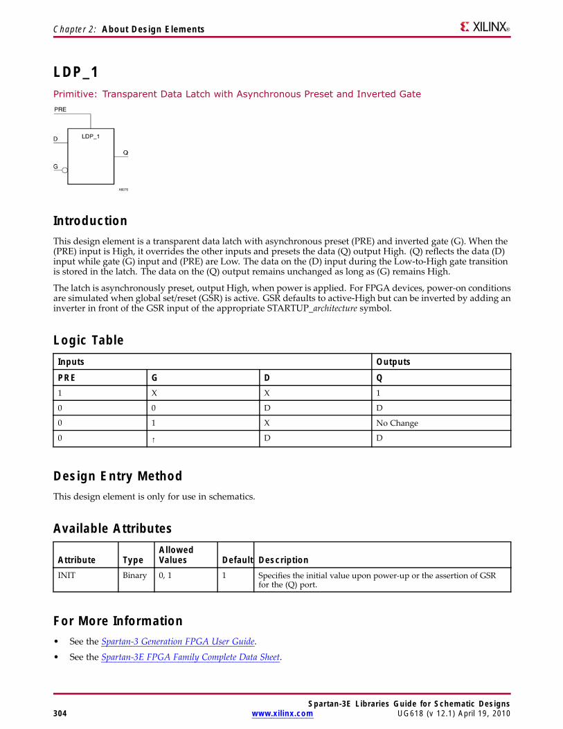
Chapter 2: About Design Elements
LDP_1Primitive: Transparent Data Latch with Asynchronous Preset and Inverted Gate
IntroductionThis design element is a transparent data latch with asynchronous preset (PRE) and inverted gate (G). When the(PRE) input is High, it overrides the other inputs and presets the data (Q) output High. (Q) reflects the data (D)input while gate (G) input and (PRE) are Low. The data on the (D) input during the Low-to-High gate transitionis stored in the latch. The data on the (Q) output remains unchanged as long as (G) remains High.
The latch is asynchronously preset, output High, when power is applied. For FPGA devices, power-on conditionsare simulated when global set/reset (GSR) is active. GSR defaults to active-High but can be inverted by adding aninverter in front of the GSR input of the appropriate STARTUP_architecture symbol.
Logic TableInputs Outputs
PRE G D Q1 X X 1
0 0 D D
0 1 X No Change
0 ↑ D D
Design Entry MethodThis design element is only for use in schematics.
Available Attributes
Attribute TypeAllowedValues Default Description
INIT Binary 0, 1 1 Specifies the initial value upon power-up or the assertion of GSRfor the (Q) port.
For More Information• See the Spartan-3 Generation FPGA User Guide.
• See the Spartan-3E FPGA Family Complete Data Sheet.
Spartan-3E Libraries Guide for Schematic Designs304 www.xilinx.com UG618 (v 12.1) April 19, 2010
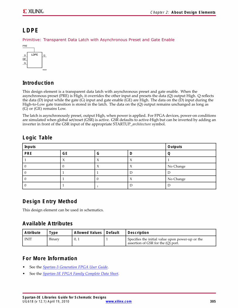
Chapter 2: About Design Elements
LDPEPrimitive: Transparent Data Latch with Asynchronous Preset and Gate Enable
IntroductionThis design element is a transparent data latch with asynchronous preset and gate enable. When theasynchronous preset (PRE) is High, it overrides the other input and presets the data (Q) output High. Q reflectsthe data (D) input while the gate (G) input and gate enable (GE) are High. The data on the (D) input during theHigh-to-Low gate transition is stored in the latch. The data on the (Q) output remains unchanged as long as(G) or (GE) remains Low.
The latch is asynchronously preset, output High, when power is applied. For FPGA devices, power-on conditionsare simulated when global set/reset (GSR) is active. GSR defaults to active-High but can be inverted by adding aninverter in front of the GSR input of the appropriate STARTUP_architecture symbol.
Logic TableInputs Outputs
PRE GE G D Q1 X X X 1
0 0 X X No Change
0 1 1 D D
0 1 0 X No Change
0 1 ↓ D D
Design Entry MethodThis design element can be used in schematics.
Available AttributesAttribute Type Allowed Values Default DescriptionINIT Binary 0, 1 1 Specifies the initial value upon power-up or the
assertion of GSR for the (Q) port.
For More Information• See the Spartan-3 Generation FPGA User Guide.
• See the Spartan-3E FPGA Family Complete Data Sheet.
Spartan-3E Libraries Guide for Schematic DesignsUG618 (v 12.1) April 19, 2010 www.xilinx.com 305
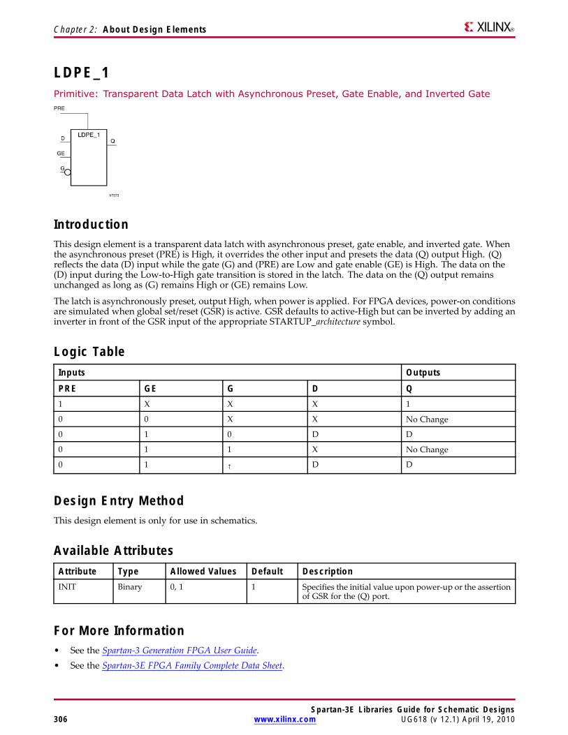
Chapter 2: About Design Elements
LDPE_1Primitive: Transparent Data Latch with Asynchronous Preset, Gate Enable, and Inverted Gate
IntroductionThis design element is a transparent data latch with asynchronous preset, gate enable, and inverted gate. Whenthe asynchronous preset (PRE) is High, it overrides the other input and presets the data (Q) output High. (Q)reflects the data (D) input while the gate (G) and (PRE) are Low and gate enable (GE) is High. The data on the(D) input during the Low-to-High gate transition is stored in the latch. The data on the (Q) output remainsunchanged as long as (G) remains High or (GE) remains Low.
The latch is asynchronously preset, output High, when power is applied. For FPGA devices, power-on conditionsare simulated when global set/reset (GSR) is active. GSR defaults to active-High but can be inverted by adding aninverter in front of the GSR input of the appropriate STARTUP_architecture symbol.
Logic TableInputs Outputs
PRE GE G D Q1 X X X 1
0 0 X X No Change
0 1 0 D D
0 1 1 X No Change
0 1 ↑ D D
Design Entry MethodThis design element is only for use in schematics.
Available AttributesAttribute Type Allowed Values Default DescriptionINIT Binary 0, 1 1 Specifies the initial value upon power-up or the assertion
of GSR for the (Q) port.
For More Information• See the Spartan-3 Generation FPGA User Guide.• See the Spartan-3E FPGA Family Complete Data Sheet.
Spartan-3E Libraries Guide for Schematic Designs306 www.xilinx.com UG618 (v 12.1) April 19, 2010
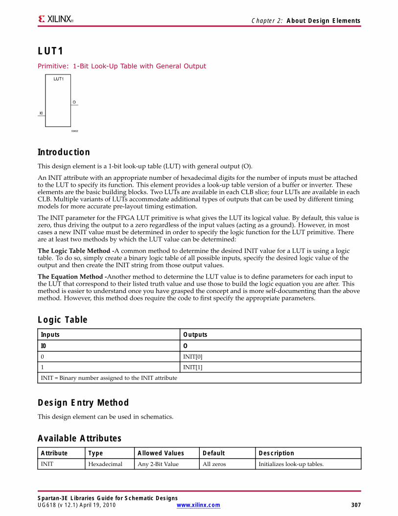
Chapter 2: About Design Elements
LUT1Primitive: 1-Bit Look-Up Table with General Output
IntroductionThis design element is a 1-bit look-up table (LUT) with general output (O).
An INIT attribute with an appropriate number of hexadecimal digits for the number of inputs must be attachedto the LUT to specify its function. This element provides a look-up table version of a buffer or inverter. Theseelements are the basic building blocks. Two LUTs are available in each CLB slice; four LUTs are available in eachCLB. Multiple variants of LUTs accommodate additional types of outputs that can be used by different timingmodels for more accurate pre-layout timing estimation.
The INIT parameter for the FPGA LUT primitive is what gives the LUT its logical value. By default, this value iszero, thus driving the output to a zero regardless of the input values (acting as a ground). However, in mostcases a new INIT value must be determined in order to specify the logic function for the LUT primitive. Thereare at least two methods by which the LUT value can be determined:
The Logic Table Method -A common method to determine the desired INIT value for a LUT is using a logictable. To do so, simply create a binary logic table of all possible inputs, specify the desired logic value of theoutput and then create the INIT string from those output values.
The Equation Method -Another method to determine the LUT value is to define parameters for each input tothe LUT that correspond to their listed truth value and use those to build the logic equation you are after. Thismethod is easier to understand once you have grasped the concept and is more self-documenting than the abovemethod. However, this method does require the code to first specify the appropriate parameters.
Logic TableInputs Outputs
I0 O0 INIT[0]
1 INIT[1]
INIT = Binary number assigned to the INIT attribute
Design Entry MethodThis design element can be used in schematics.
Available AttributesAttribute Type Allowed Values Default DescriptionINIT Hexadecimal Any 2-Bit Value All zeros Initializes look-up tables.
Spartan-3E Libraries Guide for Schematic DesignsUG618 (v 12.1) April 19, 2010 www.xilinx.com 307

Chapter 2: About Design Elements
For More Information• See the Spartan-3 Generation FPGA User Guide.
• See the Spartan-3E FPGA Family Complete Data Sheet.
Spartan-3E Libraries Guide for Schematic Designs308 www.xilinx.com UG618 (v 12.1) April 19, 2010
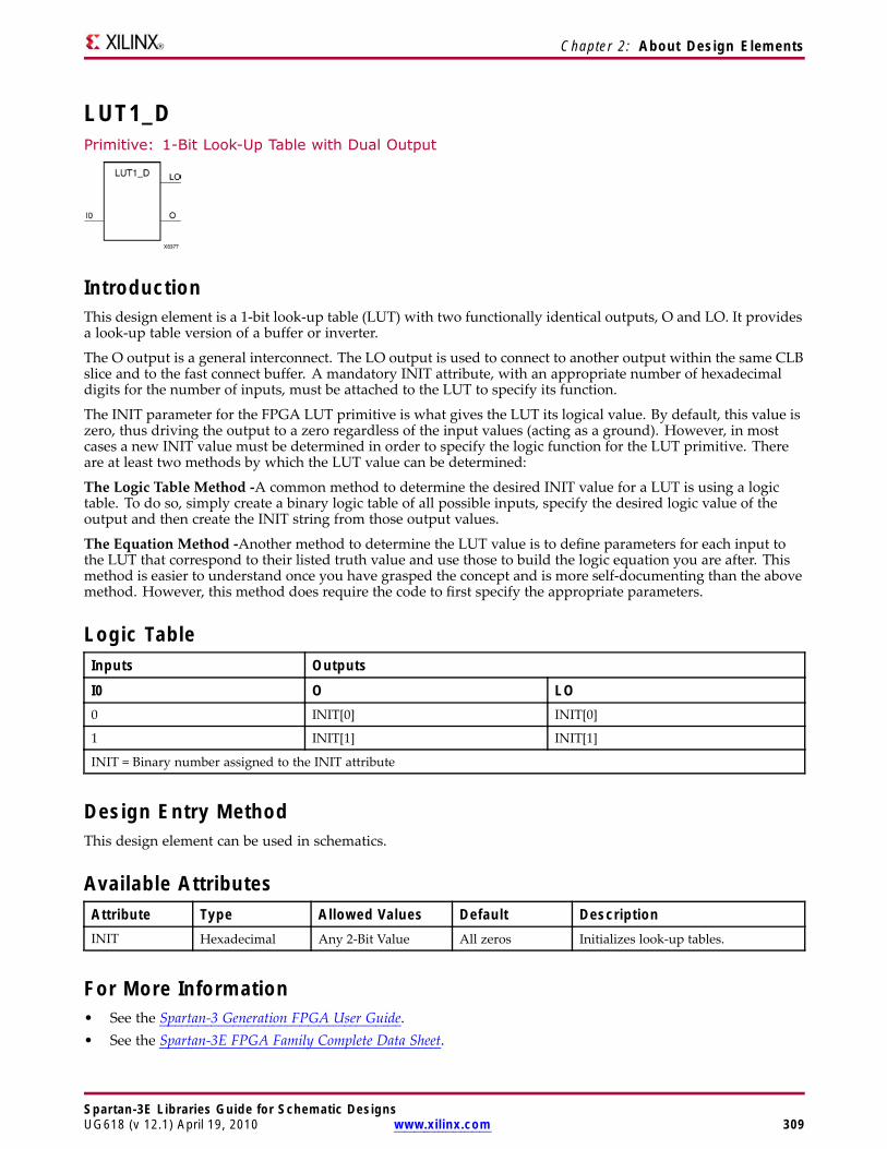
Chapter 2: About Design Elements
LUT1_DPrimitive: 1-Bit Look-Up Table with Dual Output
IntroductionThis design element is a 1-bit look-up table (LUT) with two functionally identical outputs, O and LO. It providesa look-up table version of a buffer or inverter.
The O output is a general interconnect. The LO output is used to connect to another output within the same CLBslice and to the fast connect buffer. A mandatory INIT attribute, with an appropriate number of hexadecimaldigits for the number of inputs, must be attached to the LUT to specify its function.
The INIT parameter for the FPGA LUT primitive is what gives the LUT its logical value. By default, this value iszero, thus driving the output to a zero regardless of the input values (acting as a ground). However, in mostcases a new INIT value must be determined in order to specify the logic function for the LUT primitive. Thereare at least two methods by which the LUT value can be determined:
The Logic Table Method -A common method to determine the desired INIT value for a LUT is using a logictable. To do so, simply create a binary logic table of all possible inputs, specify the desired logic value of theoutput and then create the INIT string from those output values.
The Equation Method -Another method to determine the LUT value is to define parameters for each input tothe LUT that correspond to their listed truth value and use those to build the logic equation you are after. Thismethod is easier to understand once you have grasped the concept and is more self-documenting than the abovemethod. However, this method does require the code to first specify the appropriate parameters.
Logic TableInputs Outputs
I0 O LO0 INIT[0] INIT[0]
1 INIT[1] INIT[1]
INIT = Binary number assigned to the INIT attribute
Design Entry MethodThis design element can be used in schematics.
Available AttributesAttribute Type Allowed Values Default DescriptionINIT Hexadecimal Any 2-Bit Value All zeros Initializes look-up tables.
For More Information• See the Spartan-3 Generation FPGA User Guide.• See the Spartan-3E FPGA Family Complete Data Sheet.
Spartan-3E Libraries Guide for Schematic DesignsUG618 (v 12.1) April 19, 2010 www.xilinx.com 309
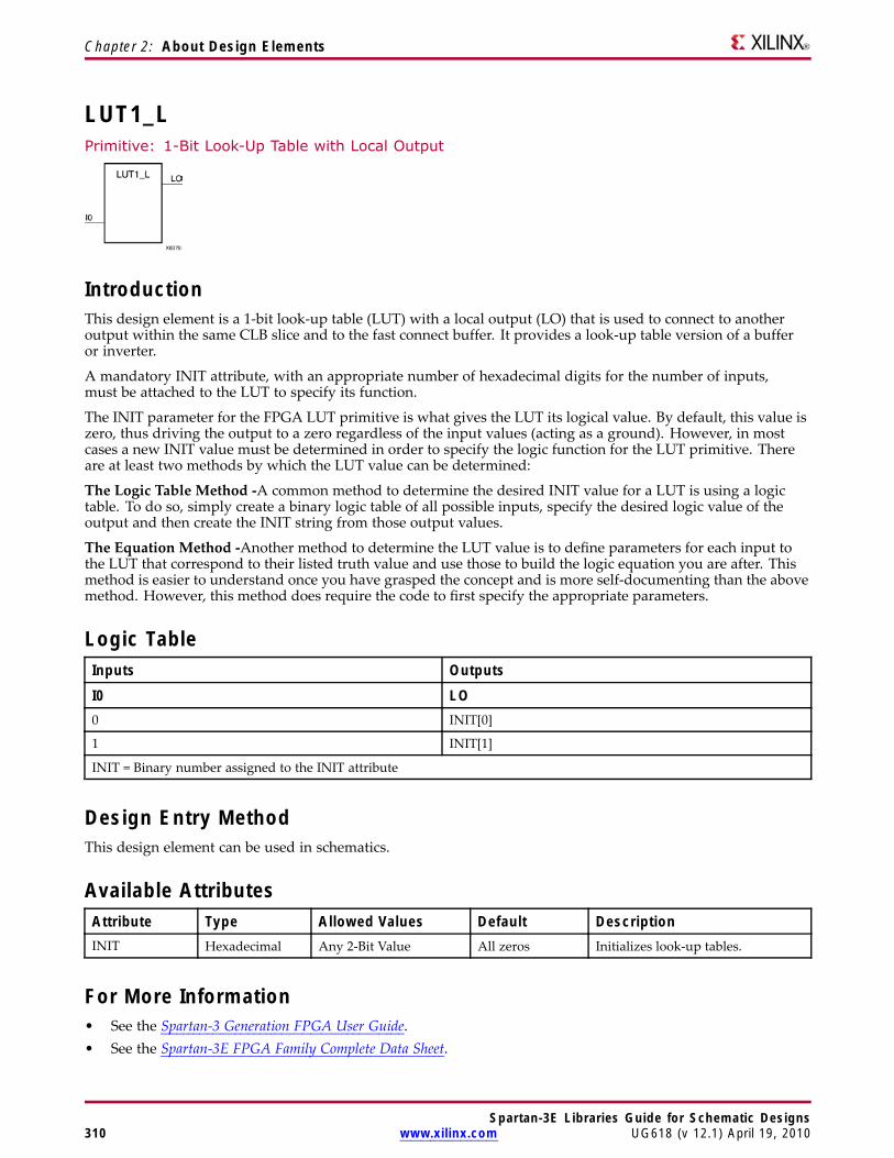
Chapter 2: About Design Elements
LUT1_LPrimitive: 1-Bit Look-Up Table with Local Output
IntroductionThis design element is a 1-bit look-up table (LUT) with a local output (LO) that is used to connect to anotheroutput within the same CLB slice and to the fast connect buffer. It provides a look-up table version of a bufferor inverter.
A mandatory INIT attribute, with an appropriate number of hexadecimal digits for the number of inputs,must be attached to the LUT to specify its function.
The INIT parameter for the FPGA LUT primitive is what gives the LUT its logical value. By default, this value iszero, thus driving the output to a zero regardless of the input values (acting as a ground). However, in mostcases a new INIT value must be determined in order to specify the logic function for the LUT primitive. Thereare at least two methods by which the LUT value can be determined:
The Logic Table Method -A common method to determine the desired INIT value for a LUT is using a logictable. To do so, simply create a binary logic table of all possible inputs, specify the desired logic value of theoutput and then create the INIT string from those output values.
The Equation Method -Another method to determine the LUT value is to define parameters for each input tothe LUT that correspond to their listed truth value and use those to build the logic equation you are after. Thismethod is easier to understand once you have grasped the concept and is more self-documenting than the abovemethod. However, this method does require the code to first specify the appropriate parameters.
Logic TableInputs Outputs
I0 LO0 INIT[0]
1 INIT[1]
INIT = Binary number assigned to the INIT attribute
Design Entry MethodThis design element can be used in schematics.
Available AttributesAttribute Type Allowed Values Default DescriptionINIT Hexadecimal Any 2-Bit Value All zeros Initializes look-up tables.
For More Information• See the Spartan-3 Generation FPGA User Guide.• See the Spartan-3E FPGA Family Complete Data Sheet.
Spartan-3E Libraries Guide for Schematic Designs310 www.xilinx.com UG618 (v 12.1) April 19, 2010
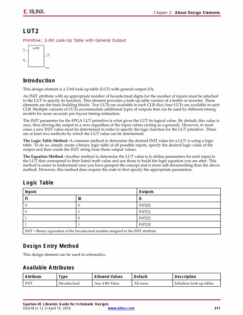
Chapter 2: About Design Elements
LUT2Primitive: 2-Bit Look-Up Table with General Output
IntroductionThis design element is a 2-bit look-up table (LUT) with general output (O).
An INIT attribute with an appropriate number of hexadecimal digits for the number of inputs must be attachedto the LUT to specify its function. This element provides a look-up table version of a buffer or inverter. Theseelements are the basic building blocks. Two LUTs are available in each CLB slice; four LUTs are available in eachCLB. Multiple variants of LUTs accommodate additional types of outputs that can be used by different timingmodels for more accurate pre-layout timing estimation.
The INIT parameter for the FPGA LUT primitive is what gives the LUT its logical value. By default, this value iszero, thus driving the output to a zero regardless of the input values (acting as a ground). However, in mostcases a new INIT value must be determined in order to specify the logic function for the LUT primitive. Thereare at least two methods by which the LUT value can be determined:
The Logic Table Method -A common method to determine the desired INIT value for a LUT is using a logictable. To do so, simply create a binary logic table of all possible inputs, specify the desired logic value of theoutput and then create the INIT string from those output values.
The Equation Method -Another method to determine the LUT value is to define parameters for each input tothe LUT that correspond to their listed truth value and use those to build the logic equation you are after. Thismethod is easier to understand once you have grasped the concept and is more self-documenting than the abovemethod. However, this method does require the code to first specify the appropriate parameters.
Logic TableInputs Outputs
I1 I0 O0 0 INIT[0]
0 1 INIT[1]
1 0 INIT[2]
1 1 INIT[3]
INIT = Binary equivalent of the hexadecimal number assigned to the INIT attribute
Design Entry MethodThis design element can be used in schematics.
Available AttributesAttribute Type Allowed Values Default DescriptionINIT Hexadecimal Any 4-Bit Value All zeros Initializes look-up tables.
Spartan-3E Libraries Guide for Schematic DesignsUG618 (v 12.1) April 19, 2010 www.xilinx.com 311

Chapter 2: About Design Elements
For More Information• See the Spartan-3 Generation FPGA User Guide.
• See the Spartan-3E FPGA Family Complete Data Sheet.
Spartan-3E Libraries Guide for Schematic Designs312 www.xilinx.com UG618 (v 12.1) April 19, 2010
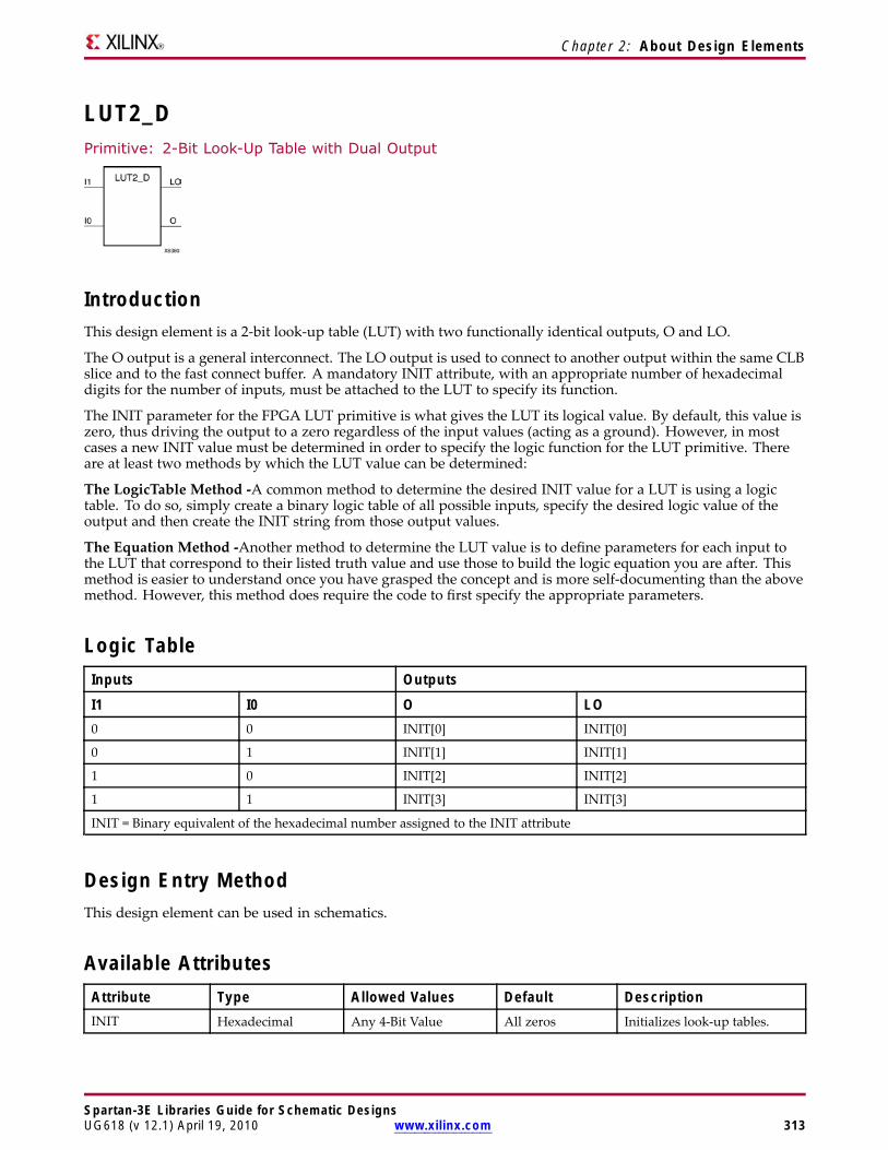
Chapter 2: About Design Elements
LUT2_DPrimitive: 2-Bit Look-Up Table with Dual Output
IntroductionThis design element is a 2-bit look-up table (LUT) with two functionally identical outputs, O and LO.
The O output is a general interconnect. The LO output is used to connect to another output within the same CLBslice and to the fast connect buffer. A mandatory INIT attribute, with an appropriate number of hexadecimaldigits for the number of inputs, must be attached to the LUT to specify its function.
The INIT parameter for the FPGA LUT primitive is what gives the LUT its logical value. By default, this value iszero, thus driving the output to a zero regardless of the input values (acting as a ground). However, in mostcases a new INIT value must be determined in order to specify the logic function for the LUT primitive. Thereare at least two methods by which the LUT value can be determined:
The LogicTable Method -A common method to determine the desired INIT value for a LUT is using a logictable. To do so, simply create a binary logic table of all possible inputs, specify the desired logic value of theoutput and then create the INIT string from those output values.
The Equation Method -Another method to determine the LUT value is to define parameters for each input tothe LUT that correspond to their listed truth value and use those to build the logic equation you are after. Thismethod is easier to understand once you have grasped the concept and is more self-documenting than the abovemethod. However, this method does require the code to first specify the appropriate parameters.
Logic TableInputs Outputs
I1 I0 O LO0 0 INIT[0] INIT[0]
0 1 INIT[1] INIT[1]
1 0 INIT[2] INIT[2]
1 1 INIT[3] INIT[3]
INIT = Binary equivalent of the hexadecimal number assigned to the INIT attribute
Design Entry MethodThis design element can be used in schematics.
Available AttributesAttribute Type Allowed Values Default DescriptionINIT Hexadecimal Any 4-Bit Value All zeros Initializes look-up tables.
Spartan-3E Libraries Guide for Schematic DesignsUG618 (v 12.1) April 19, 2010 www.xilinx.com 313

Chapter 2: About Design Elements
For More Information• See the Spartan-3 Generation FPGA User Guide.
• See the Spartan-3E FPGA Family Complete Data Sheet.
Spartan-3E Libraries Guide for Schematic Designs314 www.xilinx.com UG618 (v 12.1) April 19, 2010
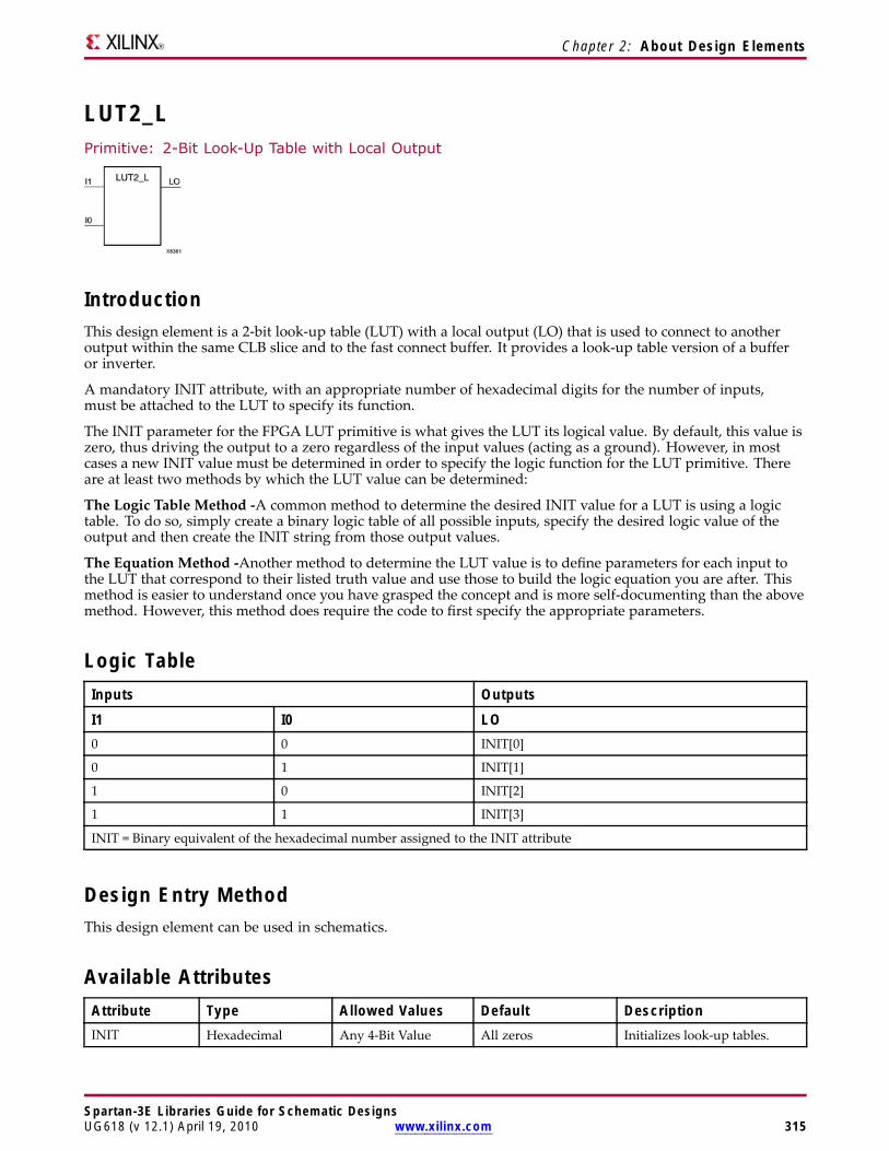
Chapter 2: About Design Elements
LUT2_LPrimitive: 2-Bit Look-Up Table with Local Output
IntroductionThis design element is a 2-bit look-up table (LUT) with a local output (LO) that is used to connect to anotheroutput within the same CLB slice and to the fast connect buffer. It provides a look-up table version of a bufferor inverter.
A mandatory INIT attribute, with an appropriate number of hexadecimal digits for the number of inputs,must be attached to the LUT to specify its function.
The INIT parameter for the FPGA LUT primitive is what gives the LUT its logical value. By default, this value iszero, thus driving the output to a zero regardless of the input values (acting as a ground). However, in mostcases a new INIT value must be determined in order to specify the logic function for the LUT primitive. Thereare at least two methods by which the LUT value can be determined:
The Logic Table Method -A common method to determine the desired INIT value for a LUT is using a logictable. To do so, simply create a binary logic table of all possible inputs, specify the desired logic value of theoutput and then create the INIT string from those output values.
The Equation Method -Another method to determine the LUT value is to define parameters for each input tothe LUT that correspond to their listed truth value and use those to build the logic equation you are after. Thismethod is easier to understand once you have grasped the concept and is more self-documenting than the abovemethod. However, this method does require the code to first specify the appropriate parameters.
Logic TableInputs Outputs
I1 I0 LO0 0 INIT[0]
0 1 INIT[1]
1 0 INIT[2]
1 1 INIT[3]
INIT = Binary equivalent of the hexadecimal number assigned to the INIT attribute
Design Entry MethodThis design element can be used in schematics.
Available AttributesAttribute Type Allowed Values Default DescriptionINIT Hexadecimal Any 4-Bit Value All zeros Initializes look-up tables.
Spartan-3E Libraries Guide for Schematic DesignsUG618 (v 12.1) April 19, 2010 www.xilinx.com 315

Chapter 2: About Design Elements
For More Information• See the Spartan-3 Generation FPGA User Guide.
• See the Spartan-3E FPGA Family Complete Data Sheet.
Spartan-3E Libraries Guide for Schematic Designs316 www.xilinx.com UG618 (v 12.1) April 19, 2010
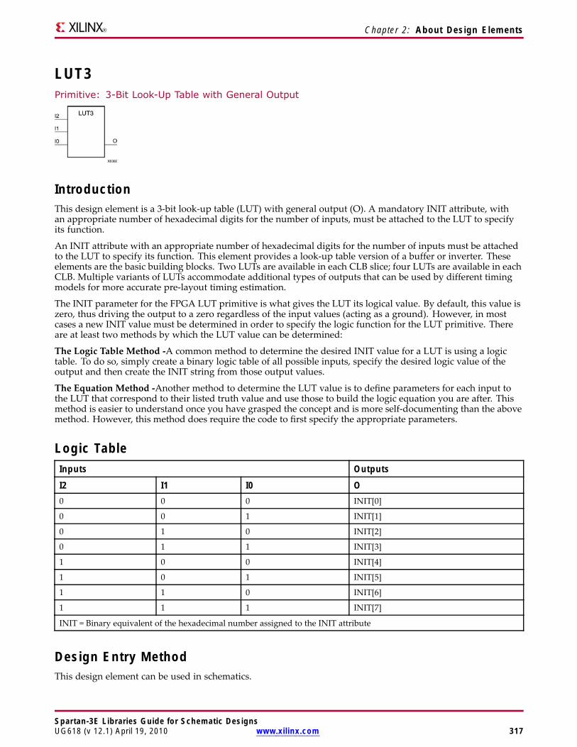
Chapter 2: About Design Elements
LUT3Primitive: 3-Bit Look-Up Table with General Output
IntroductionThis design element is a 3-bit look-up table (LUT) with general output (O). A mandatory INIT attribute, withan appropriate number of hexadecimal digits for the number of inputs, must be attached to the LUT to specifyits function.
An INIT attribute with an appropriate number of hexadecimal digits for the number of inputs must be attachedto the LUT to specify its function. This element provides a look-up table version of a buffer or inverter. Theseelements are the basic building blocks. Two LUTs are available in each CLB slice; four LUTs are available in eachCLB. Multiple variants of LUTs accommodate additional types of outputs that can be used by different timingmodels for more accurate pre-layout timing estimation.
The INIT parameter for the FPGA LUT primitive is what gives the LUT its logical value. By default, this value iszero, thus driving the output to a zero regardless of the input values (acting as a ground). However, in mostcases a new INIT value must be determined in order to specify the logic function for the LUT primitive. Thereare at least two methods by which the LUT value can be determined:
The Logic Table Method -A common method to determine the desired INIT value for a LUT is using a logictable. To do so, simply create a binary logic table of all possible inputs, specify the desired logic value of theoutput and then create the INIT string from those output values.
The Equation Method -Another method to determine the LUT value is to define parameters for each input tothe LUT that correspond to their listed truth value and use those to build the logic equation you are after. Thismethod is easier to understand once you have grasped the concept and is more self-documenting than the abovemethod. However, this method does require the code to first specify the appropriate parameters.
Logic TableInputs Outputs
I2 I1 I0 O0 0 0 INIT[0]
0 0 1 INIT[1]
0 1 0 INIT[2]
0 1 1 INIT[3]
1 0 0 INIT[4]
1 0 1 INIT[5]
1 1 0 INIT[6]
1 1 1 INIT[7]
INIT = Binary equivalent of the hexadecimal number assigned to the INIT attribute
Design Entry MethodThis design element can be used in schematics.
Spartan-3E Libraries Guide for Schematic DesignsUG618 (v 12.1) April 19, 2010 www.xilinx.com 317
Chapter 2: About Design Elements
Available AttributesAttribute Type Allowed Values Default DescriptionINIT Hexadecimal Any 8-Bit Value All zeros Initializes look-up tables.
For More Information• See the Spartan-3 Generation FPGA User Guide.
• See the Spartan-3E FPGA Family Complete Data Sheet.
Spartan-3E Libraries Guide for Schematic Designs318 www.xilinx.com UG618 (v 12.1) April 19, 2010
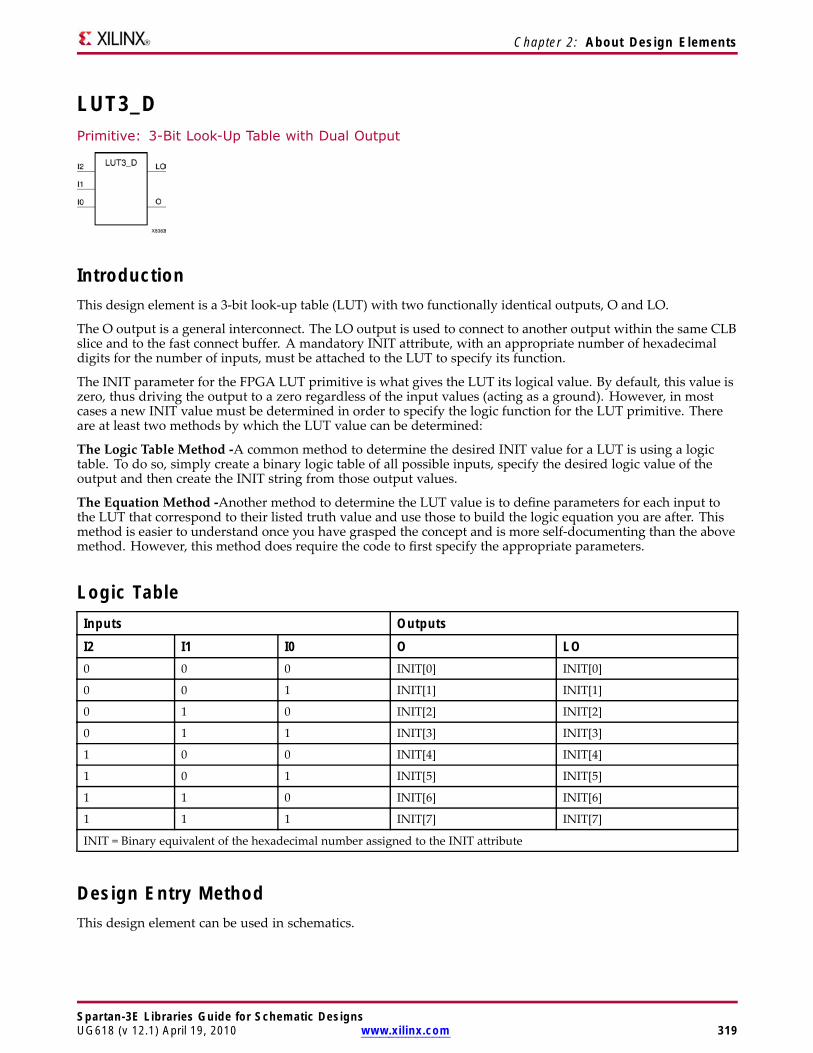
Chapter 2: About Design Elements
LUT3_DPrimitive: 3-Bit Look-Up Table with Dual Output
IntroductionThis design element is a 3-bit look-up table (LUT) with two functionally identical outputs, O and LO.
The O output is a general interconnect. The LO output is used to connect to another output within the same CLBslice and to the fast connect buffer. A mandatory INIT attribute, with an appropriate number of hexadecimaldigits for the number of inputs, must be attached to the LUT to specify its function.
The INIT parameter for the FPGA LUT primitive is what gives the LUT its logical value. By default, this value iszero, thus driving the output to a zero regardless of the input values (acting as a ground). However, in mostcases a new INIT value must be determined in order to specify the logic function for the LUT primitive. Thereare at least two methods by which the LUT value can be determined:
The Logic Table Method -A common method to determine the desired INIT value for a LUT is using a logictable. To do so, simply create a binary logic table of all possible inputs, specify the desired logic value of theoutput and then create the INIT string from those output values.
The Equation Method -Another method to determine the LUT value is to define parameters for each input tothe LUT that correspond to their listed truth value and use those to build the logic equation you are after. Thismethod is easier to understand once you have grasped the concept and is more self-documenting than the abovemethod. However, this method does require the code to first specify the appropriate parameters.
Logic TableInputs Outputs
I2 I1 I0 O LO0 0 0 INIT[0] INIT[0]
0 0 1 INIT[1] INIT[1]
0 1 0 INIT[2] INIT[2]
0 1 1 INIT[3] INIT[3]
1 0 0 INIT[4] INIT[4]
1 0 1 INIT[5] INIT[5]
1 1 0 INIT[6] INIT[6]
1 1 1 INIT[7] INIT[7]
INIT = Binary equivalent of the hexadecimal number assigned to the INIT attribute
Design Entry MethodThis design element can be used in schematics.
Spartan-3E Libraries Guide for Schematic DesignsUG618 (v 12.1) April 19, 2010 www.xilinx.com 319
Chapter 2: About Design Elements
Available AttributesAttribute Type Allowed Values Default DescriptionINIT Hexadecimal Any 8-Bit Value All zeros Initializes look-up tables.
For More Information• See the Spartan-3 Generation FPGA User Guide.
• See the Spartan-3E FPGA Family Complete Data Sheet.
Spartan-3E Libraries Guide for Schematic Designs320 www.xilinx.com UG618 (v 12.1) April 19, 2010
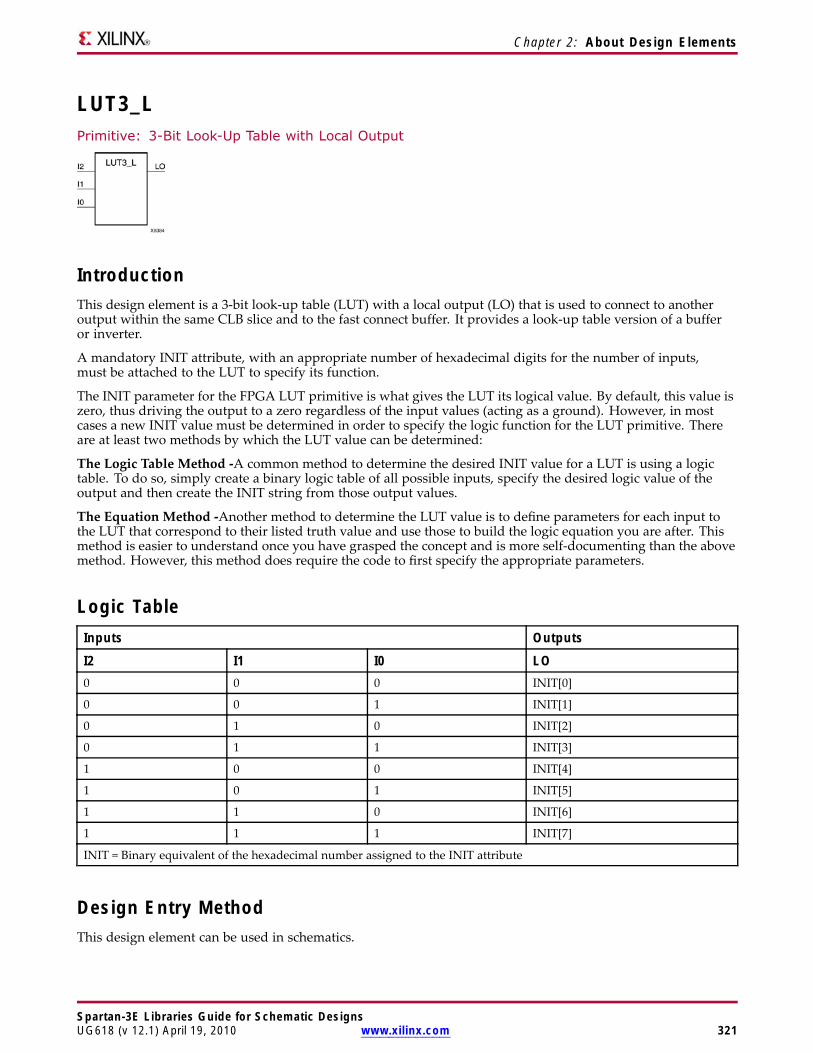
Chapter 2: About Design Elements
LUT3_LPrimitive: 3-Bit Look-Up Table with Local Output
IntroductionThis design element is a 3-bit look-up table (LUT) with a local output (LO) that is used to connect to anotheroutput within the same CLB slice and to the fast connect buffer. It provides a look-up table version of a bufferor inverter.
A mandatory INIT attribute, with an appropriate number of hexadecimal digits for the number of inputs,must be attached to the LUT to specify its function.
The INIT parameter for the FPGA LUT primitive is what gives the LUT its logical value. By default, this value iszero, thus driving the output to a zero regardless of the input values (acting as a ground). However, in mostcases a new INIT value must be determined in order to specify the logic function for the LUT primitive. Thereare at least two methods by which the LUT value can be determined:
The Logic Table Method -A common method to determine the desired INIT value for a LUT is using a logictable. To do so, simply create a binary logic table of all possible inputs, specify the desired logic value of theoutput and then create the INIT string from those output values.
The Equation Method -Another method to determine the LUT value is to define parameters for each input tothe LUT that correspond to their listed truth value and use those to build the logic equation you are after. Thismethod is easier to understand once you have grasped the concept and is more self-documenting than the abovemethod. However, this method does require the code to first specify the appropriate parameters.
Logic TableInputs Outputs
I2 I1 I0 LO0 0 0 INIT[0]
0 0 1 INIT[1]
0 1 0 INIT[2]
0 1 1 INIT[3]
1 0 0 INIT[4]
1 0 1 INIT[5]
1 1 0 INIT[6]
1 1 1 INIT[7]
INIT = Binary equivalent of the hexadecimal number assigned to the INIT attribute
Design Entry MethodThis design element can be used in schematics.
Spartan-3E Libraries Guide for Schematic DesignsUG618 (v 12.1) April 19, 2010 www.xilinx.com 321

Chapter 2: About Design Elements
Available AttributesAttribute Type Allowed Values Default DescriptionINIT Hexadecimal Any 8-Bit Value All zeros Initializes look-up tables.
For More Information• See the Spartan-3 Generation FPGA User Guide.
• See the Spartan-3E FPGA Family Complete Data Sheet.
Spartan-3E Libraries Guide for Schematic Designs322 www.xilinx.com UG618 (v 12.1) April 19, 2010

Chapter 2: About Design Elements
LUT4Primitive: 4-Bit Look-Up-Table with General Output
IntroductionThis design element is a 4-bit look-up table (LUT) with general output (O).
An INIT attribute with an appropriate number of hexadecimal digits for the number of inputs must be attachedto the LUT to specify its function. This element provides a look-up table version of a buffer or inverter. Theseelements are the basic building blocks. Two LUTs are available in each CLB slice; four LUTs are available in eachCLB. Multiple variants of LUTs accommodate additional types of outputs that can be used by different timingmodels for more accurate pre-layout timing estimation.
The INIT parameter for the FPGA LUT primitive is what gives the LUT its logical value. By default, this value iszero, thus driving the output to a zero regardless of the input values (acting as a ground). However, in mostcases a new INIT value must be determined in order to specify the logic function for the LUT primitive. Thereare at least two methods by which the LUT value can be determined:
The Logic Table Method -A common method to determine the desired INIT value for a LUT is using a logictable. To do so, simply create a binary logic table of all possible inputs, specify the desired logic value of theoutput and then create the INIT string from those output values.
The Equation Method -Another method to determine the LUT value is to define parameters for each input tothe LUT that correspond to their listed truth value and use those to build the logic equation you are after. Thismethod is easier to understand once you have grasped the concept and is more self-documenting than the abovemethod. However, this method does require the code to first specify the appropriate parameters.
Spartan-3E Libraries Guide for Schematic DesignsUG618 (v 12.1) April 19, 2010 www.xilinx.com 323
Chapter 2: About Design Elements
Logic TableInputs Outputs
I3 I2 I1 I0 O0 0 0 0 INIT[0]
0 0 0 1 INIT[1]
0 0 1 0 INIT[2]
0 0 1 1 INIT[3]
0 1 0 0 INIT[4]
0 1 0 1 INIT[5]
0 1 1 0 INIT[6]
0 1 1 1 INIT[7]
1 0 0 0 INIT[8]
1 0 0 1 INIT[9]
1 0 1 0 INIT[10]
1 0 1 1 INIT[11]
1 1 0 0 INIT[12]
1 1 0 1 INIT[13]
1 1 1 0 INIT[14]
1 1 1 1 INIT[15]
INIT = Binary equivalent of the hexadecimal number assigned to the INIT attribute
Design Entry MethodThis design element can be used in schematics.
Available AttributesAttribute Type Allowed Values Default DescriptionINIT Hexadecimal Any 16-Bit Value All zeros Initializes look-up tables.
For More Information• See the Spartan-3 Generation FPGA User Guide.
• See the Spartan-3E FPGA Family Complete Data Sheet.
Spartan-3E Libraries Guide for Schematic Designs324 www.xilinx.com UG618 (v 12.1) April 19, 2010
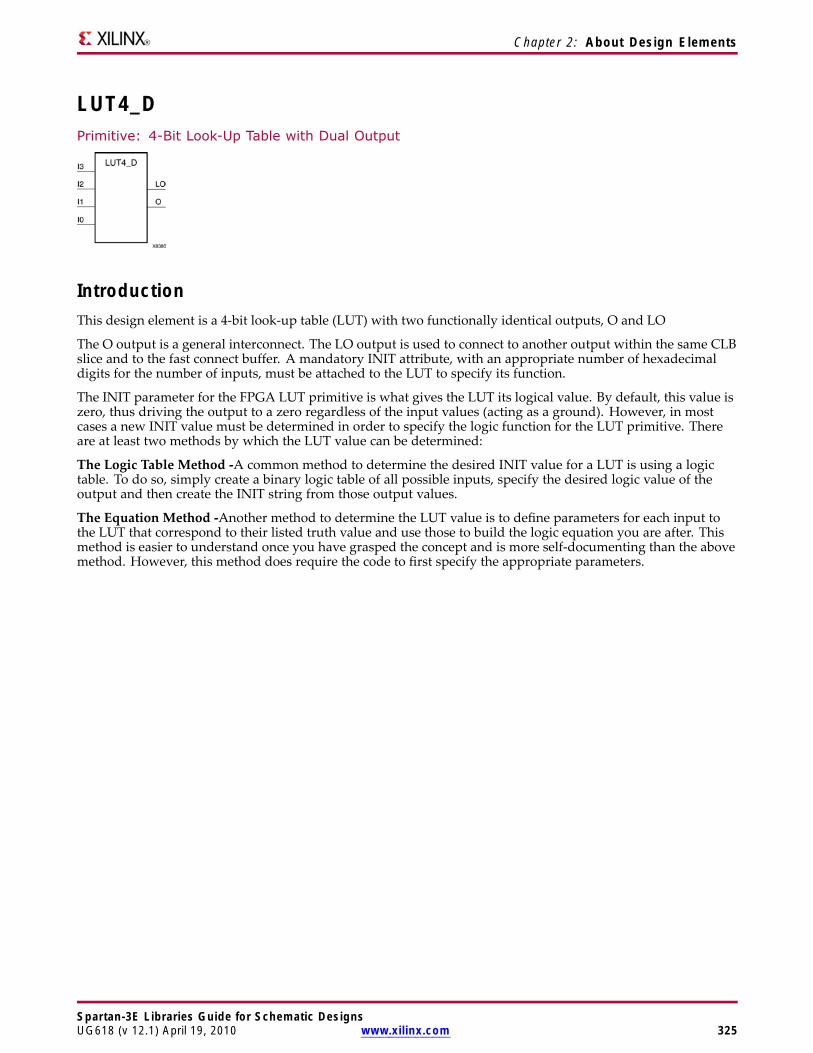
Chapter 2: About Design Elements
LUT4_DPrimitive: 4-Bit Look-Up Table with Dual Output
IntroductionThis design element is a 4-bit look-up table (LUT) with two functionally identical outputs, O and LO
The O output is a general interconnect. The LO output is used to connect to another output within the same CLBslice and to the fast connect buffer. A mandatory INIT attribute, with an appropriate number of hexadecimaldigits for the number of inputs, must be attached to the LUT to specify its function.
The INIT parameter for the FPGA LUT primitive is what gives the LUT its logical value. By default, this value iszero, thus driving the output to a zero regardless of the input values (acting as a ground). However, in mostcases a new INIT value must be determined in order to specify the logic function for the LUT primitive. Thereare at least two methods by which the LUT value can be determined:
The Logic Table Method -A common method to determine the desired INIT value for a LUT is using a logictable. To do so, simply create a binary logic table of all possible inputs, specify the desired logic value of theoutput and then create the INIT string from those output values.
The Equation Method -Another method to determine the LUT value is to define parameters for each input tothe LUT that correspond to their listed truth value and use those to build the logic equation you are after. Thismethod is easier to understand once you have grasped the concept and is more self-documenting than the abovemethod. However, this method does require the code to first specify the appropriate parameters.
Spartan-3E Libraries Guide for Schematic DesignsUG618 (v 12.1) April 19, 2010 www.xilinx.com 325
Chapter 2: About Design Elements
Logic TableInputs Outputs
I3 I2 I1 I0 O LO0 0 0 0 INIT[0] INIT[0]
0 0 0 1 INIT[1] INIT[1]
0 0 1 0 INIT[2] INIT[2]
0 0 1 1 INIT[3] INIT[3]
0 1 0 0 INIT[4] INIT[4]
0 1 0 1 INIT[5] INIT[5]
0 1 1 0 INIT[6] INIT[6]
0 1 1 1 INIT[7] INIT[7]
1 0 0 0 INIT[8] INIT[8]
1 0 0 1 INIT[9] INIT[9]
1 0 1 0 INIT[10] INIT[10]
1 0 1 1 INIT[11] INIT[11]
1 1 0 0 INIT[12] INIT[12]
1 1 0 1 INIT[13] INIT[13]
1 1 1 0 INIT[14] INIT[14]
1 1 1 1 INIT[15] INIT[15]
INIT = Binary equivalent of the hexadecimal number assigned to the INIT attribute
Design Entry MethodThis design element can be used in schematics.
Available AttributesAttribute Type Allowed Values Default DescriptionINIT Hexadecimal Any 16-Bit Value All zeros Initializes look-up tables.
For More Information• See the Spartan-3 Generation FPGA User Guide.
• See the Spartan-3E FPGA Family Complete Data Sheet.
Spartan-3E Libraries Guide for Schematic Designs326 www.xilinx.com UG618 (v 12.1) April 19, 2010
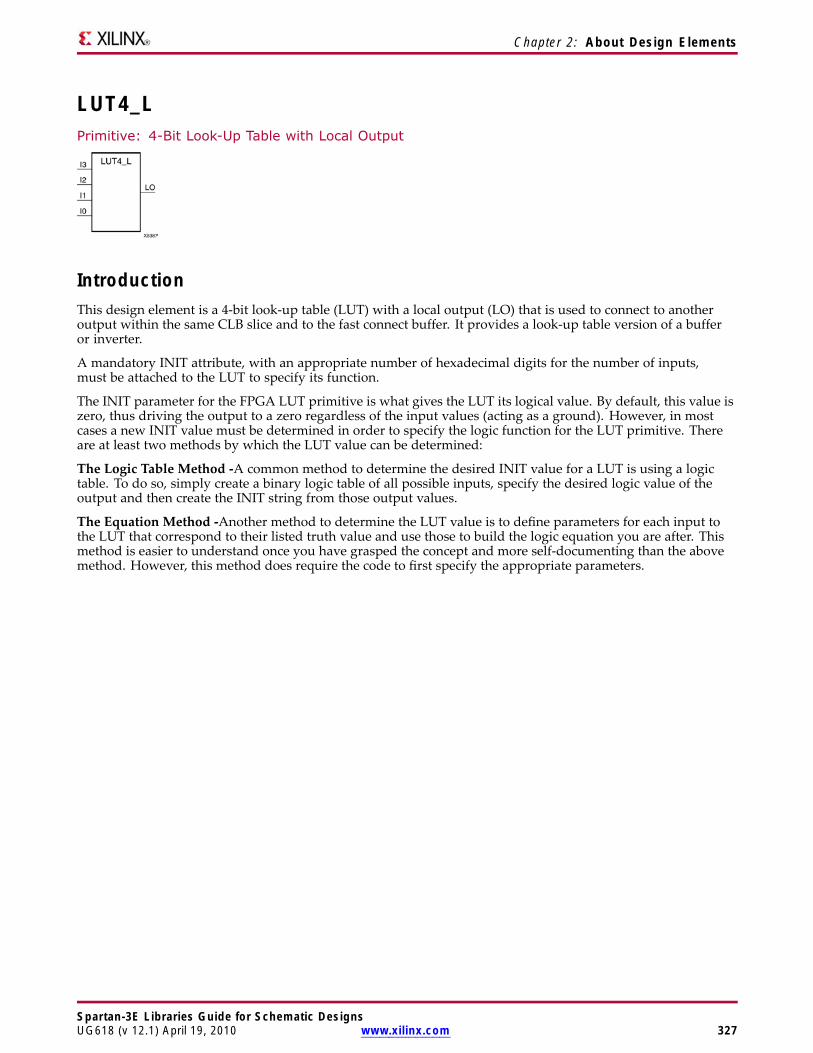
Chapter 2: About Design Elements
LUT4_LPrimitive: 4-Bit Look-Up Table with Local Output
IntroductionThis design element is a 4-bit look-up table (LUT) with a local output (LO) that is used to connect to anotheroutput within the same CLB slice and to the fast connect buffer. It provides a look-up table version of a bufferor inverter.
A mandatory INIT attribute, with an appropriate number of hexadecimal digits for the number of inputs,must be attached to the LUT to specify its function.
The INIT parameter for the FPGA LUT primitive is what gives the LUT its logical value. By default, this value iszero, thus driving the output to a zero regardless of the input values (acting as a ground). However, in mostcases a new INIT value must be determined in order to specify the logic function for the LUT primitive. Thereare at least two methods by which the LUT value can be determined:
The Logic Table Method -A common method to determine the desired INIT value for a LUT is using a logictable. To do so, simply create a binary logic table of all possible inputs, specify the desired logic value of theoutput and then create the INIT string from those output values.
The Equation Method -Another method to determine the LUT value is to define parameters for each input tothe LUT that correspond to their listed truth value and use those to build the logic equation you are after. Thismethod is easier to understand once you have grasped the concept and more self-documenting than the abovemethod. However, this method does require the code to first specify the appropriate parameters.
Spartan-3E Libraries Guide for Schematic DesignsUG618 (v 12.1) April 19, 2010 www.xilinx.com 327

Chapter 2: About Design Elements
Logic TableInputs Outputs
I3 I2 I1 I0 LO0 0 0 0 INIT[0]
0 0 0 1 INIT[1]
0 0 1 0 INIT[2]
0 0 1 1 INIT[3]
0 1 0 0 INIT[4]
0 1 0 1 INIT[5]
0 1 1 0 INIT[6]
0 1 1 1 INIT[7]
1 0 0 0 INIT[8]
1 0 0 1 INIT[9]
1 0 1 0 INIT[10]
1 0 1 1 INIT[11]
1 1 0 0 INIT[12]
1 1 0 1 INIT[13]
1 1 1 0 INIT[14]
1 1 1 1 INIT[15]
INIT = Binary equivalent of the hexadecimal number assigned to the INIT attribute
Design Entry MethodThis design element can be used in schematics.
Available AttributesAttribute Type Allowed Values Default DescriptionINIT Hexadecimal Any 16-Bit Value All zeros Initializes look-up tables.
For More Information• See the Spartan-3 Generation FPGA User Guide.
• See the Spartan-3E FPGA Family Complete Data Sheet.
Spartan-3E Libraries Guide for Schematic Designs328 www.xilinx.com UG618 (v 12.1) April 19, 2010
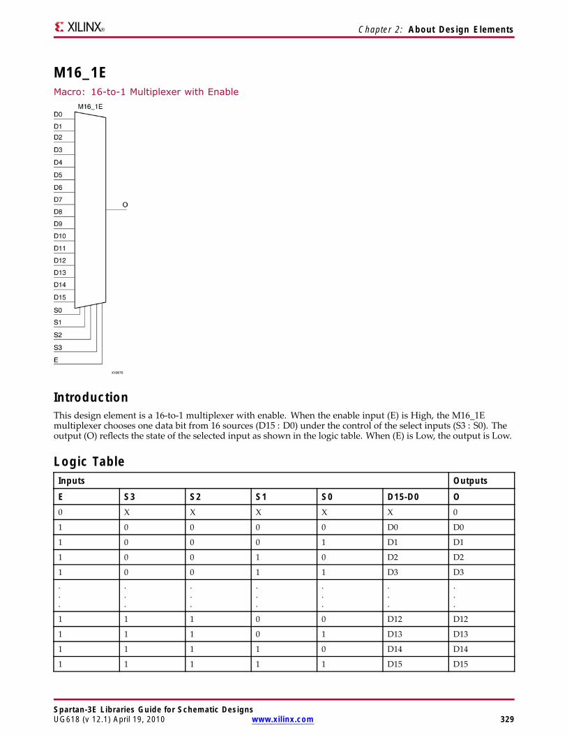
Chapter 2: About Design Elements
M16_1EMacro: 16-to-1 Multiplexer with Enable
IntroductionThis design element is a 16-to-1 multiplexer with enable. When the enable input (E) is High, the M16_1Emultiplexer chooses one data bit from 16 sources (D15 : D0) under the control of the select inputs (S3 : S0). Theoutput (O) reflects the state of the selected input as shown in the logic table. When (E) is Low, the output is Low.
Logic TableInputs Outputs
E S3 S2 S1 S0 D15-D0 O0 X X X X X 0
1 0 0 0 0 D0 D0
1 0 0 0 1 D1 D1
1 0 0 1 0 D2 D2
1 0 0 1 1 D3 D3...
.
.
.
.
.
.
.
.
.
.
.
.
.
.
.
.
.
.
1 1 1 0 0 D12 D12
1 1 1 0 1 D13 D13
1 1 1 1 0 D14 D14
1 1 1 1 1 D15 D15
Spartan-3E Libraries Guide for Schematic DesignsUG618 (v 12.1) April 19, 2010 www.xilinx.com 329

Chapter 2: About Design Elements
Design Entry MethodThis design element is only for use in schematics.
For More Information• See the Spartan-3 Generation FPGA User Guide.
• See the Spartan-3E FPGA Family Complete Data Sheet.
Spartan-3E Libraries Guide for Schematic Designs330 www.xilinx.com UG618 (v 12.1) April 19, 2010
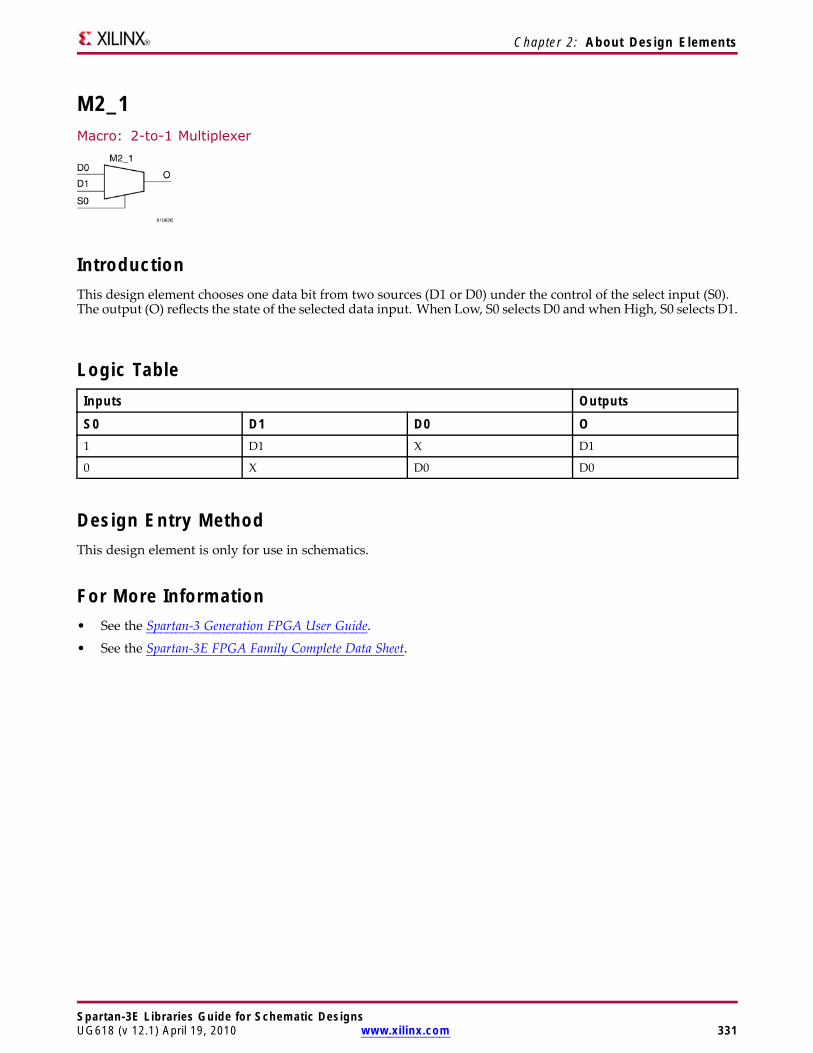
Chapter 2: About Design Elements
M2_1Macro: 2-to-1 Multiplexer
IntroductionThis design element chooses one data bit from two sources (D1 or D0) under the control of the select input (S0).The output (O) reflects the state of the selected data input. When Low, S0 selects D0 and when High, S0 selects D1.
Logic TableInputs Outputs
S0 D1 D0 O1 D1 X D1
0 X D0 D0
Design Entry MethodThis design element is only for use in schematics.
For More Information• See the Spartan-3 Generation FPGA User Guide.
• See the Spartan-3E FPGA Family Complete Data Sheet.
Spartan-3E Libraries Guide for Schematic DesignsUG618 (v 12.1) April 19, 2010 www.xilinx.com 331
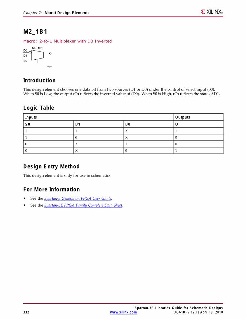
Chapter 2: About Design Elements
M2_1B1Macro: 2-to-1 Multiplexer with D0 Inverted
IntroductionThis design element chooses one data bit from two sources (D1 or D0) under the control of select input (S0).When S0 is Low, the output (O) reflects the inverted value of (D0). When S0 is High, (O) reflects the state of D1.
Logic TableInputs Outputs
S0 D1 D0 O1 1 X 1
1 0 X 0
0 X 1 0
0 X 0 1
Design Entry MethodThis design element is only for use in schematics.
For More Information• See the Spartan-3 Generation FPGA User Guide.
• See the Spartan-3E FPGA Family Complete Data Sheet.
Spartan-3E Libraries Guide for Schematic Designs332 www.xilinx.com UG618 (v 12.1) April 19, 2010
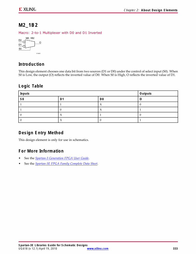
Chapter 2: About Design Elements
M2_1B2Macro: 2-to-1 Multiplexer with D0 and D1 Inverted
IntroductionThis design element chooses one data bit from two sources (D1 or D0) under the control of select input (S0). WhenS0 is Low, the output (O) reflects the inverted value of D0. When S0 is High, O reflects the inverted value of D1.
Logic TableInputs Outputs
S0 D1 D0 O1 1 X 0
1 0 X 1
0 X 1 0
0 X 0 1
Design Entry MethodThis design element is only for use in schematics.
For More Information• See the Spartan-3 Generation FPGA User Guide.
• See the Spartan-3E FPGA Family Complete Data Sheet.
Spartan-3E Libraries Guide for Schematic DesignsUG618 (v 12.1) April 19, 2010 www.xilinx.com 333
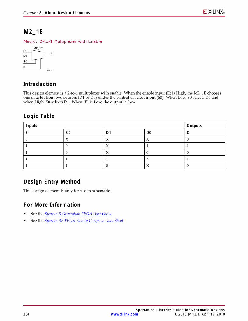
Chapter 2: About Design Elements
M2_1EMacro: 2-to-1 Multiplexer with Enable
IntroductionThis design element is a 2-to-1 multiplexer with enable. When the enable input (E) is High, the M2_1E choosesone data bit from two sources (D1 or D0) under the control of select input (S0). When Low, S0 selects D0 andwhen High, S0 selects D1. When (E) is Low, the output is Low.
Logic TableInputs Outputs
E S0 D1 D0 O0 X X X 0
1 0 X 1 1
1 0 X 0 0
1 1 1 X 1
1 1 0 X 0
Design Entry MethodThis design element is only for use in schematics.
For More Information• See the Spartan-3 Generation FPGA User Guide.
• See the Spartan-3E FPGA Family Complete Data Sheet.
Spartan-3E Libraries Guide for Schematic Designs334 www.xilinx.com UG618 (v 12.1) April 19, 2010
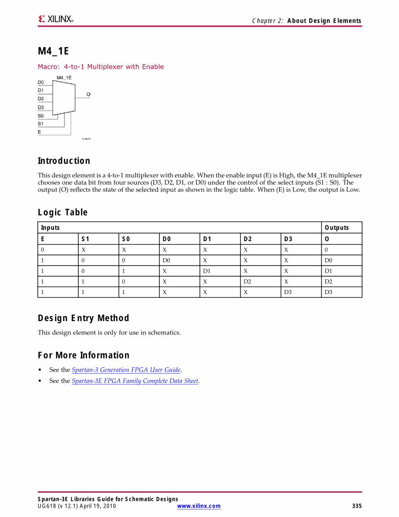
Chapter 2: About Design Elements
M4_1EMacro: 4-to-1 Multiplexer with Enable
IntroductionThis design element is a 4-to-1 multiplexer with enable. When the enable input (E) is High, the M4_1Emultiplexerchooses one data bit from four sources (D3, D2, D1, or D0) under the control of the select inputs (S1 : S0). Theoutput (O) reflects the state of the selected input as shown in the logic table. When (E) is Low, the output is Low.
Logic TableInputs Outputs
E S1 S0 D0 D1 D2 D3 O0 X X X X X X 0
1 0 0 D0 X X X D0
1 0 1 X D1 X X D1
1 1 0 X X D2 X D2
1 1 1 X X X D3 D3
Design Entry MethodThis design element is only for use in schematics.
For More Information• See the Spartan-3 Generation FPGA User Guide.
• See the Spartan-3E FPGA Family Complete Data Sheet.
Spartan-3E Libraries Guide for Schematic DesignsUG618 (v 12.1) April 19, 2010 www.xilinx.com 335
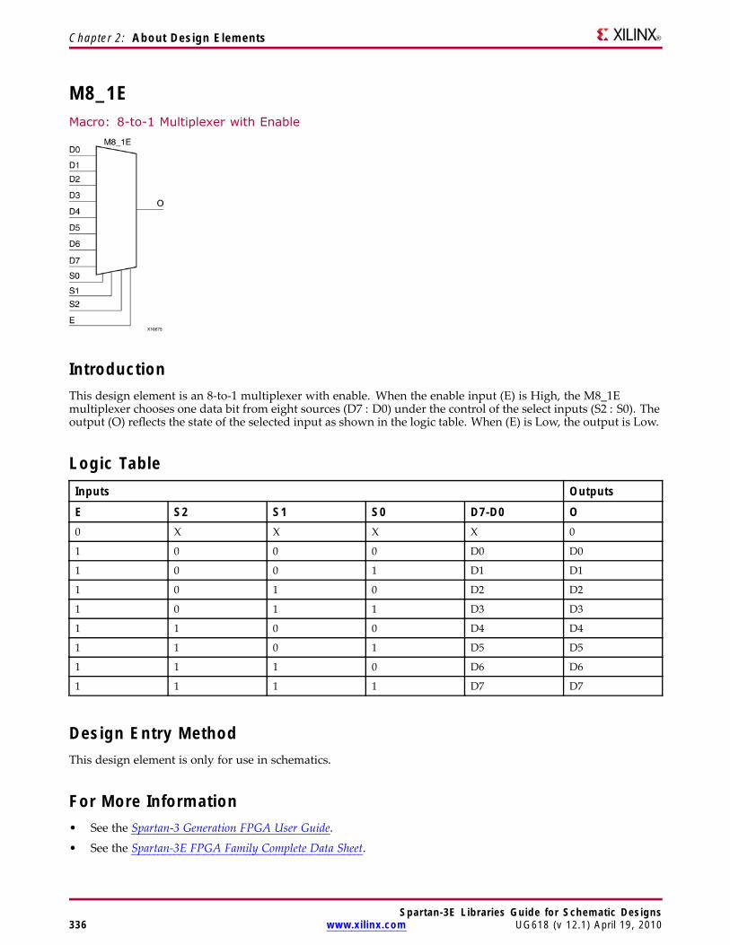
Chapter 2: About Design Elements
M8_1EMacro: 8-to-1 Multiplexer with Enable
IntroductionThis design element is an 8-to-1 multiplexer with enable. When the enable input (E) is High, the M8_1Emultiplexer chooses one data bit from eight sources (D7 : D0) under the control of the select inputs (S2 : S0). Theoutput (O) reflects the state of the selected input as shown in the logic table. When (E) is Low, the output is Low.
Logic TableInputs Outputs
E S2 S1 S0 D7-D0 O0 X X X X 0
1 0 0 0 D0 D0
1 0 0 1 D1 D1
1 0 1 0 D2 D2
1 0 1 1 D3 D3
1 1 0 0 D4 D4
1 1 0 1 D5 D5
1 1 1 0 D6 D6
1 1 1 1 D7 D7
Design Entry MethodThis design element is only for use in schematics.
For More Information• See the Spartan-3 Generation FPGA User Guide.
• See the Spartan-3E FPGA Family Complete Data Sheet.
Spartan-3E Libraries Guide for Schematic Designs336 www.xilinx.com UG618 (v 12.1) April 19, 2010
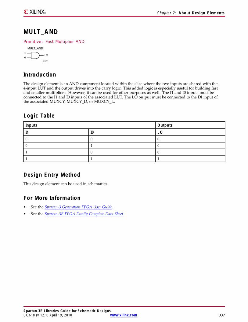
Chapter 2: About Design Elements
MULT_ANDPrimitive: Fast Multiplier AND
IntroductionThe design element is an AND component located within the slice where the two inputs are shared with the4-input LUT and the output drives into the carry logic. This added logic is especially useful for building fastand smaller multipliers. However, it can be used for other purposes as well. The I1 and I0 inputs must beconnected to the I1 and I0 inputs of the associated LUT. The LO output must be connected to the DI input ofthe associated MUXCY, MUXCY_D, or MUXCY_L.
Logic TableInputs Outputs
I1 I0 LO0 0 0
0 1 0
1 0 0
1 1 1
Design Entry MethodThis design element can be used in schematics.
For More Information• See the Spartan-3 Generation FPGA User Guide.
• See the Spartan-3E FPGA Family Complete Data Sheet.
Spartan-3E Libraries Guide for Schematic DesignsUG618 (v 12.1) April 19, 2010 www.xilinx.com 337
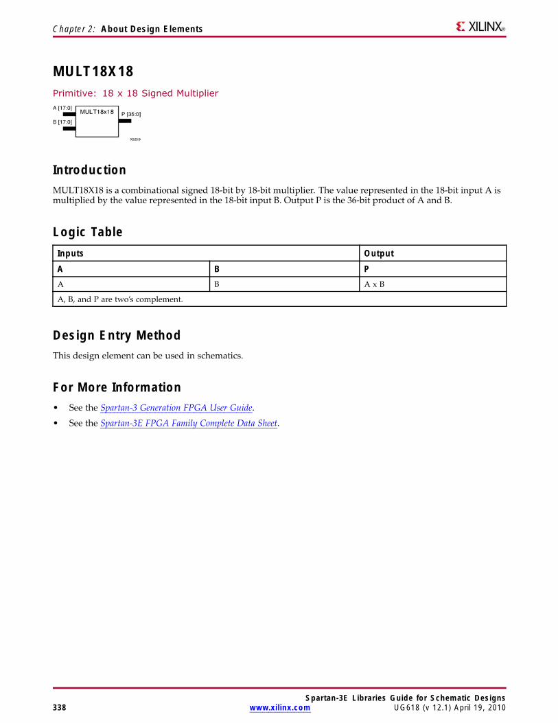
Chapter 2: About Design Elements
MULT18X18Primitive: 18 x 18 Signed Multiplier
IntroductionMULT18X18 is a combinational signed 18-bit by 18-bit multiplier. The value represented in the 18-bit input A ismultiplied by the value represented in the 18-bit input B. Output P is the 36-bit product of A and B.
Logic TableInputs OutputA B PA B A x B
A, B, and P are two’s complement.
Design Entry MethodThis design element can be used in schematics.
For More Information• See the Spartan-3 Generation FPGA User Guide.
• See the Spartan-3E FPGA Family Complete Data Sheet.
Spartan-3E Libraries Guide for Schematic Designs338 www.xilinx.com UG618 (v 12.1) April 19, 2010
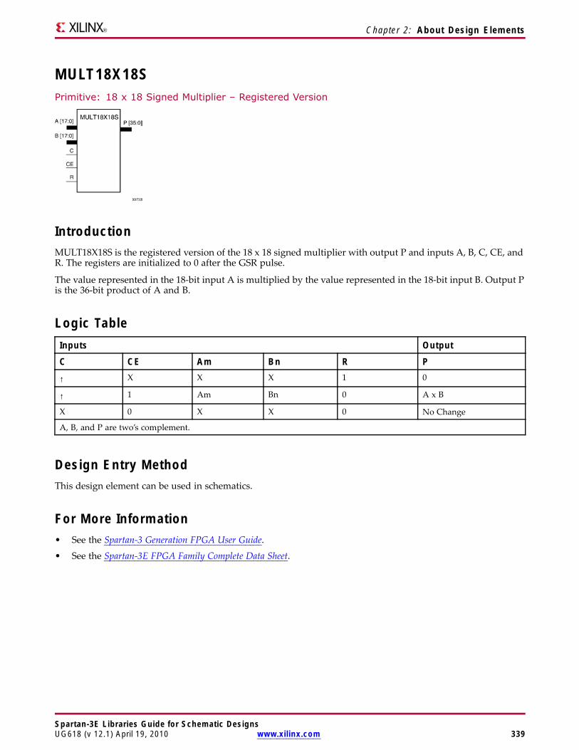
Chapter 2: About Design Elements
MULT18X18SPrimitive: 18 x 18 Signed Multiplier – Registered Version
IntroductionMULT18X18S is the registered version of the 18 x 18 signed multiplier with output P and inputs A, B, C, CE, andR. The registers are initialized to 0 after the GSR pulse.
The value represented in the 18-bit input A is multiplied by the value represented in the 18-bit input B. Output Pis the 36-bit product of A and B.
Logic TableInputs Output
C CE Am Bn R P
↑ X X X 1 0
↑ 1 Am Bn 0 A x B
X 0 X X 0 No Change
A, B, and P are two’s complement.
Design Entry MethodThis design element can be used in schematics.
For More Information• See the Spartan-3 Generation FPGA User Guide.
• See the Spartan-3E FPGA Family Complete Data Sheet.
Spartan-3E Libraries Guide for Schematic DesignsUG618 (v 12.1) April 19, 2010 www.xilinx.com 339
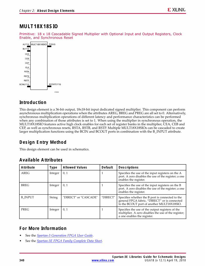
Chapter 2: About Design Elements
MULT18X18SIOPrimitive: 18 x 18 Cascadable Signed Multiplier with Optional Input and Output Registers, ClockEnable, and Synchronous Reset
IntroductionThis design element is a 36-bit output, 18x18-bit input dedicated signed multiplier. This component can performasynchronous multiplication operations when the attributes AREG, BREG and PREG are all set to 0. Alternatively,synchronous multiplication operations of different latency and performance characteristics can be performedwhen any combination of those attributes is set to 1. When using the multiplier in synchronous operation, theMULT18X18SIO features active high clock enables for each set of register banks in the multiplier, CEA, CEB andCEP, as well as synchronous resets, RSTA, RSTB, and RSTP. Multiple MULT18X18SIOs can be cascaded to createlarger multiplication functions using the BCIN and BCOUT ports in combination with the B_INPUT attribute.
Design Entry MethodThis design element can be used in schematics.
Available AttributesAttribute Type Allowed Values Default DescriptionsAREG Integer 0, 1 1 Specifies the use of the input registers on the A
port. A zero disables the use of the register; a oneenables the register.
BREG Integer 0, 1 1 Specifies the use of the input registers on the Bport. A zero disables the use of the register; a oneenables the register.
B_INPUT String "DIRECT" or "CASCADE" "DIRECT" Specifies whether the B port is connected to thegeneral FPGA fabric, “DIRECT” or is connectedto the BCOUT port of another MULT18X18SIO.
PREG Integer 0, 1 1 Specifies the use of the output registers of themultiplier. A zero disables the use of the register;a one enables the register.
For More Information• See the Spartan-3 Generation FPGA User Guide.• See the Spartan-3E FPGA Family Complete Data Sheet.
Spartan-3E Libraries Guide for Schematic Designs340 www.xilinx.com UG618 (v 12.1) April 19, 2010
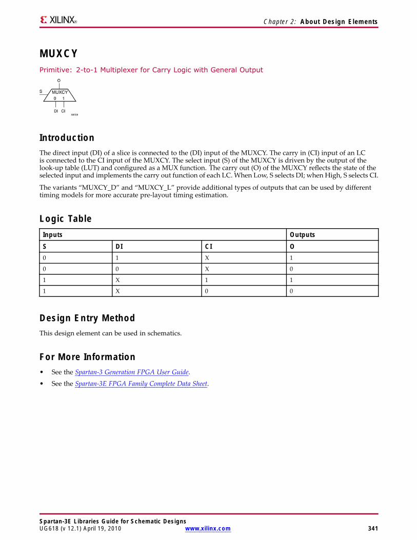
Chapter 2: About Design Elements
MUXCYPrimitive: 2-to-1 Multiplexer for Carry Logic with General Output
IntroductionThe direct input (DI) of a slice is connected to the (DI) input of the MUXCY. The carry in (CI) input of an LCis connected to the CI input of the MUXCY. The select input (S) of the MUXCY is driven by the output of thelook-up table (LUT) and configured as a MUX function. The carry out (O) of the MUXCY reflects the state of theselected input and implements the carry out function of each LC. When Low, S selects DI; when High, S selects CI.
The variants “MUXCY_D” and “MUXCY_L” provide additional types of outputs that can be used by differenttiming models for more accurate pre-layout timing estimation.
Logic TableInputs Outputs
S DI CI O0 1 X 1
0 0 X 0
1 X 1 1
1 X 0 0
Design Entry MethodThis design element can be used in schematics.
For More Information• See the Spartan-3 Generation FPGA User Guide.
• See the Spartan-3E FPGA Family Complete Data Sheet.
Spartan-3E Libraries Guide for Schematic DesignsUG618 (v 12.1) April 19, 2010 www.xilinx.com 341
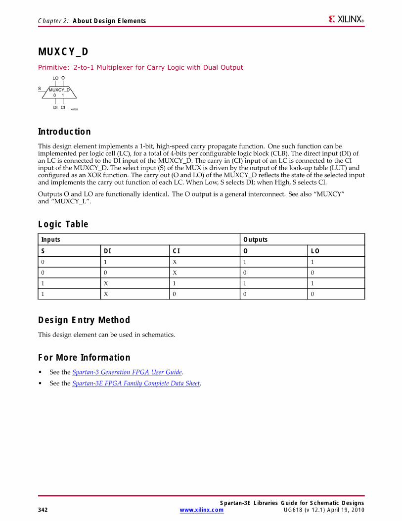
Chapter 2: About Design Elements
MUXCY_DPrimitive: 2-to-1 Multiplexer for Carry Logic with Dual Output
IntroductionThis design element implements a 1-bit, high-speed carry propagate function. One such function can beimplemented per logic cell (LC), for a total of 4-bits per configurable logic block (CLB). The direct input (DI) ofan LC is connected to the DI input of the MUXCY_D. The carry in (CI) input of an LC is connected to the CIinput of the MUXCY_D. The select input (S) of the MUX is driven by the output of the look-up table (LUT) andconfigured as an XOR function. The carry out (O and LO) of the MUXCY_D reflects the state of the selected inputand implements the carry out function of each LC. When Low, S selects DI; when High, S selects CI.
Outputs O and LO are functionally identical. The O output is a general interconnect. See also “MUXCY”and “MUXCY_L”.
Logic TableInputs Outputs
S DI CI O LO0 1 X 1 1
0 0 X 0 0
1 X 1 1 1
1 X 0 0 0
Design Entry MethodThis design element can be used in schematics.
For More Information• See the Spartan-3 Generation FPGA User Guide.
• See the Spartan-3E FPGA Family Complete Data Sheet.
Spartan-3E Libraries Guide for Schematic Designs342 www.xilinx.com UG618 (v 12.1) April 19, 2010
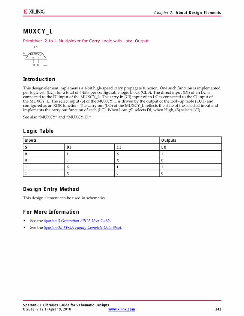
Chapter 2: About Design Elements
MUXCY_LPrimitive: 2-to-1 Multiplexer for Carry Logic with Local Output
IntroductionThis design element implements a 1-bit high-speed carry propagate function. One such function is implementedper logic cell (LC), for a total of 4-bits per configurable logic block (CLB). The direct input (DI) of an LC isconnected to the DI input of the MUXCY_L. The carry in (CI) input of an LC is connected to the CI input ofthe MUXCY_L. The select input (S) of the MUXCY_L is driven by the output of the look-up table (LUT) andconfigured as an XOR function. The carry out (LO) of the MUXCY_L reflects the state of the selected input andimplements the carry out function of each (LC). When Low, (S) selects DI; when High, (S) selects (CI).
See also “MUXCY” and “MUXCY_D.”
Logic TableInputs Outputs
S DI CI LO0 1 X 1
0 0 X 0
1 X 1 1
1 X 0 0
Design Entry MethodThis design element can be used in schematics.
For More Information• See the Spartan-3 Generation FPGA User Guide.
• See the Spartan-3E FPGA Family Complete Data Sheet.
Spartan-3E Libraries Guide for Schematic DesignsUG618 (v 12.1) April 19, 2010 www.xilinx.com 343
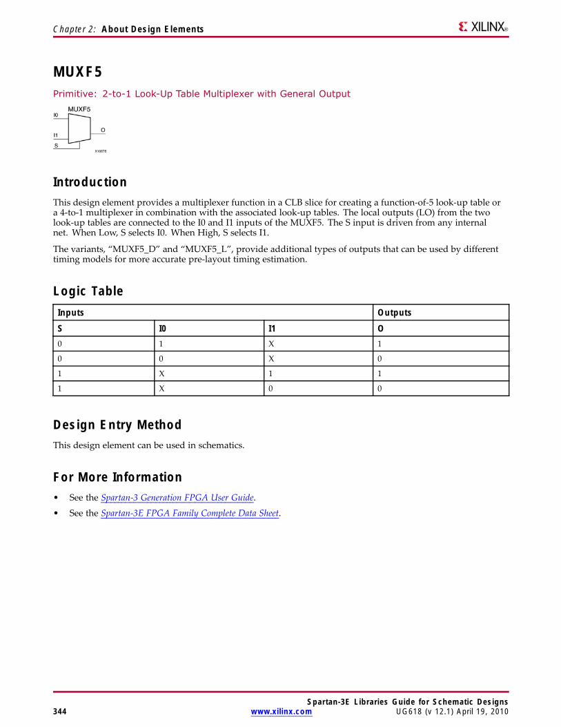
Chapter 2: About Design Elements
MUXF5Primitive: 2-to-1 Look-Up Table Multiplexer with General Output
IntroductionThis design element provides a multiplexer function in a CLB slice for creating a function-of-5 look-up table ora 4-to-1 multiplexer in combination with the associated look-up tables. The local outputs (LO) from the twolook-up tables are connected to the I0 and I1 inputs of the MUXF5. The S input is driven from any internalnet. When Low, S selects I0. When High, S selects I1.
The variants, “MUXF5_D” and “MUXF5_L”, provide additional types of outputs that can be used by differenttiming models for more accurate pre-layout timing estimation.
Logic TableInputs Outputs
S I0 I1 O0 1 X 1
0 0 X 0
1 X 1 1
1 X 0 0
Design Entry MethodThis design element can be used in schematics.
For More Information• See the Spartan-3 Generation FPGA User Guide.
• See the Spartan-3E FPGA Family Complete Data Sheet.
Spartan-3E Libraries Guide for Schematic Designs344 www.xilinx.com UG618 (v 12.1) April 19, 2010
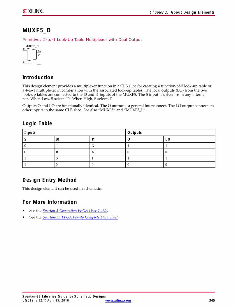
Chapter 2: About Design Elements
MUXF5_DPrimitive: 2-to-1 Look-Up Table Multiplexer with Dual Output
IntroductionThis design element provides a multiplexer function in a CLB slice for creating a function-of-5 look-up table ora 4-to-1 multiplexer in combination with the associated look-up tables. The local outputs (LO) from the twolook-up tables are connected to the I0 and I1 inputs of the MUXF5. The S input is driven from any internalnet. When Low, S selects I0. When High, S selects I1.
Outputs O and LO are functionally identical. The O output is a general interconnect. The LO output connects toother inputs in the same CLB slice. See also “MUXF5” and “MUXF5_L”.
Logic TableInputs Outputs
S I0 I1 O LO0 1 X 1 1
0 0 X 0 0
1 X 1 1 1
1 X 0 0 0
Design Entry MethodThis design element can be used in schematics.
For More Information• See the Spartan-3 Generation FPGA User Guide.
• See the Spartan-3E FPGA Family Complete Data Sheet.
Spartan-3E Libraries Guide for Schematic DesignsUG618 (v 12.1) April 19, 2010 www.xilinx.com 345
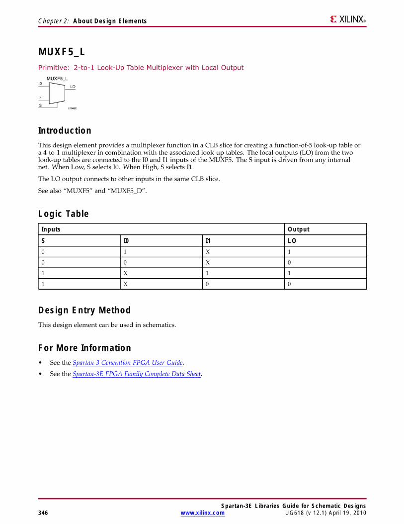
Chapter 2: About Design Elements
MUXF5_LPrimitive: 2-to-1 Look-Up Table Multiplexer with Local Output
IntroductionThis design element provides a multiplexer function in a CLB slice for creating a function-of-5 look-up table ora 4-to-1 multiplexer in combination with the associated look-up tables. The local outputs (LO) from the twolook-up tables are connected to the I0 and I1 inputs of the MUXF5. The S input is driven from any internalnet. When Low, S selects I0. When High, S selects I1.
The LO output connects to other inputs in the same CLB slice.
See also “MUXF5” and “MUXF5_D”.
Logic TableInputs Output
S I0 I1 LO0 1 X 1
0 0 X 0
1 X 1 1
1 X 0 0
Design Entry MethodThis design element can be used in schematics.
For More Information• See the Spartan-3 Generation FPGA User Guide.
• See the Spartan-3E FPGA Family Complete Data Sheet.
Spartan-3E Libraries Guide for Schematic Designs346 www.xilinx.com UG618 (v 12.1) April 19, 2010
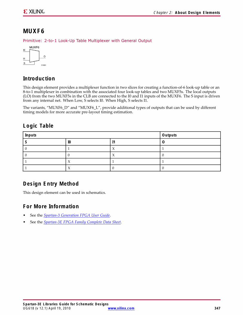
Chapter 2: About Design Elements
MUXF6Primitive: 2-to-1 Look-Up Table Multiplexer with General Output
IntroductionThis design element provides a multiplexer function in two slices for creating a function-of-6 look-up table or an8-to-1 multiplexer in combination with the associated four look-up tables and two MUXF5s. The local outputs(LO) from the two MUXF5s in the CLB are connected to the I0 and I1 inputs of the MUXF6. The S input is drivenfrom any internal net. When Low, S selects I0. When High, S selects I1.
The variants, “MUXF6_D” and “MUXF6_L”, provide additional types of outputs that can be used by differenttiming models for more accurate pre-layout timing estimation.
Logic TableInputs Outputs
S I0 I1 O0 1 X 1
0 0 X 0
1 X 1 1
1 X 0 0
Design Entry MethodThis design element can be used in schematics.
For More Information• See the Spartan-3 Generation FPGA User Guide.
• See the Spartan-3E FPGA Family Complete Data Sheet.
Spartan-3E Libraries Guide for Schematic DesignsUG618 (v 12.1) April 19, 2010 www.xilinx.com 347
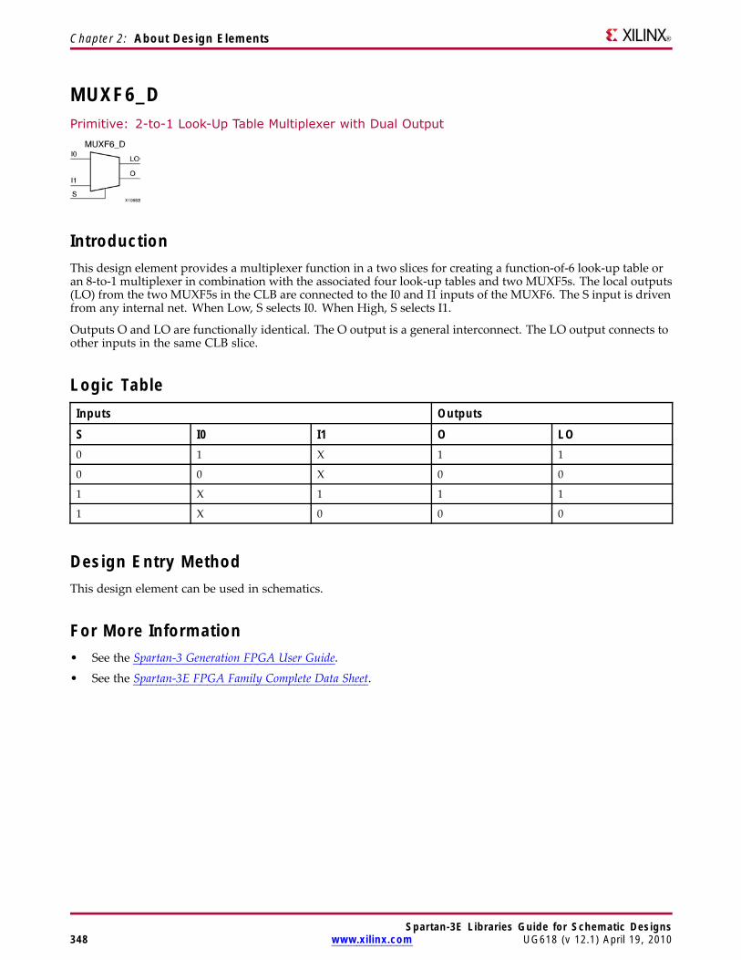
Chapter 2: About Design Elements
MUXF6_DPrimitive: 2-to-1 Look-Up Table Multiplexer with Dual Output
IntroductionThis design element provides a multiplexer function in a two slices for creating a function-of-6 look-up table oran 8-to-1 multiplexer in combination with the associated four look-up tables and two MUXF5s. The local outputs(LO) from the two MUXF5s in the CLB are connected to the I0 and I1 inputs of the MUXF6. The S input is drivenfrom any internal net. When Low, S selects I0. When High, S selects I1.
Outputs O and LO are functionally identical. The O output is a general interconnect. The LO output connects toother inputs in the same CLB slice.
Logic TableInputs Outputs
S I0 I1 O LO0 1 X 1 1
0 0 X 0 0
1 X 1 1 1
1 X 0 0 0
Design Entry MethodThis design element can be used in schematics.
For More Information• See the Spartan-3 Generation FPGA User Guide.
• See the Spartan-3E FPGA Family Complete Data Sheet.
Spartan-3E Libraries Guide for Schematic Designs348 www.xilinx.com UG618 (v 12.1) April 19, 2010
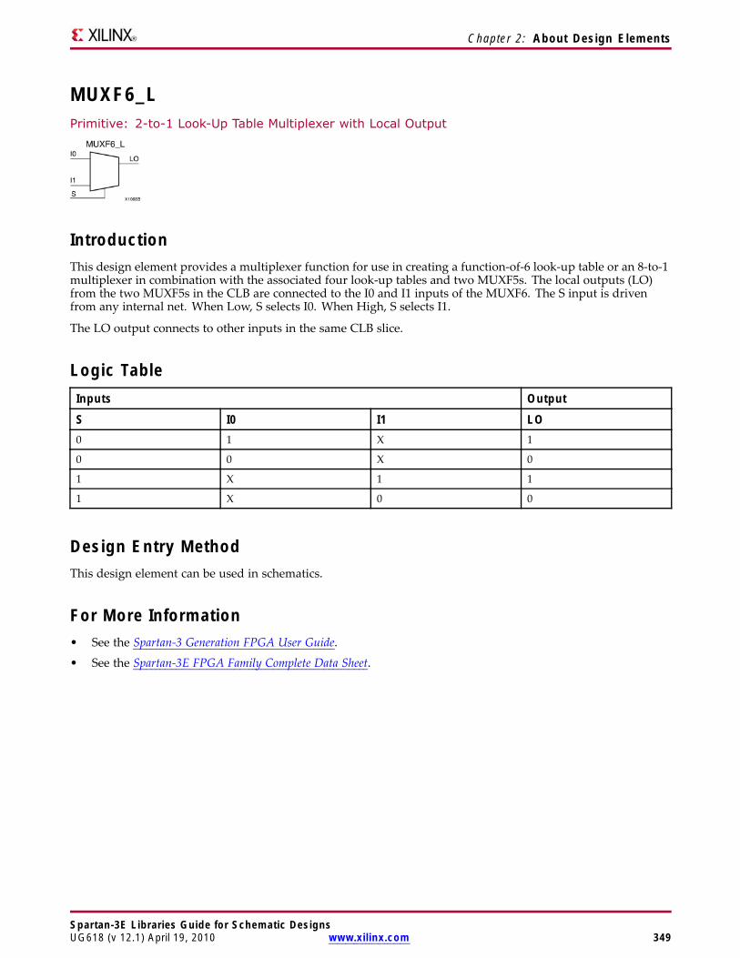
Chapter 2: About Design Elements
MUXF6_LPrimitive: 2-to-1 Look-Up Table Multiplexer with Local Output
IntroductionThis design element provides a multiplexer function for use in creating a function-of-6 look-up table or an 8-to-1multiplexer in combination with the associated four look-up tables and two MUXF5s. The local outputs (LO)from the two MUXF5s in the CLB are connected to the I0 and I1 inputs of the MUXF6. The S input is drivenfrom any internal net. When Low, S selects I0. When High, S selects I1.
The LO output connects to other inputs in the same CLB slice.
Logic TableInputs Output
S I0 I1 LO0 1 X 1
0 0 X 0
1 X 1 1
1 X 0 0
Design Entry MethodThis design element can be used in schematics.
For More Information• See the Spartan-3 Generation FPGA User Guide.
• See the Spartan-3E FPGA Family Complete Data Sheet.
Spartan-3E Libraries Guide for Schematic DesignsUG618 (v 12.1) April 19, 2010 www.xilinx.com 349
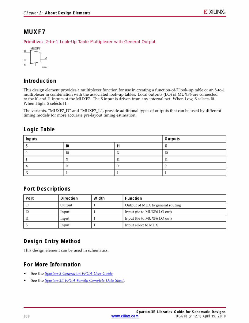
Chapter 2: About Design Elements
MUXF7Primitive: 2-to-1 Look-Up Table Multiplexer with General Output
IntroductionThis design element provides a multiplexer function for use in creating a function-of-7 look-up table or an 8-to-1multiplexer in combination with the associated look-up tables. Local outputs (LO) of MUXF6 are connectedto the I0 and I1 inputs of the MUXF7. The S input is driven from any internal net. When Low, S selects I0.When High, S selects I1.
The variants, “MUXF7_D” and “MUXF7_L”, provide additional types of outputs that can be used by differenttiming models for more accurate pre-layout timing estimation.
Logic TableInputs Outputs
S I0 I1 O0 I0 X I0
1 X I1 I1
X 0 0 0
X 1 1 1
Port DescriptionsPort Direction Width FunctionO Output 1 Output of MUX to general routing
I0 Input 1 Input (tie to MUXF6 LO out)
I1 Input 1 Input (tie to MUXF6 LO out)
S Input 1 Input select to MUX
Design Entry MethodThis design element can be used in schematics.
For More Information• See the Spartan-3 Generation FPGA User Guide.
• See the Spartan-3E FPGA Family Complete Data Sheet.
Spartan-3E Libraries Guide for Schematic Designs350 www.xilinx.com UG618 (v 12.1) April 19, 2010
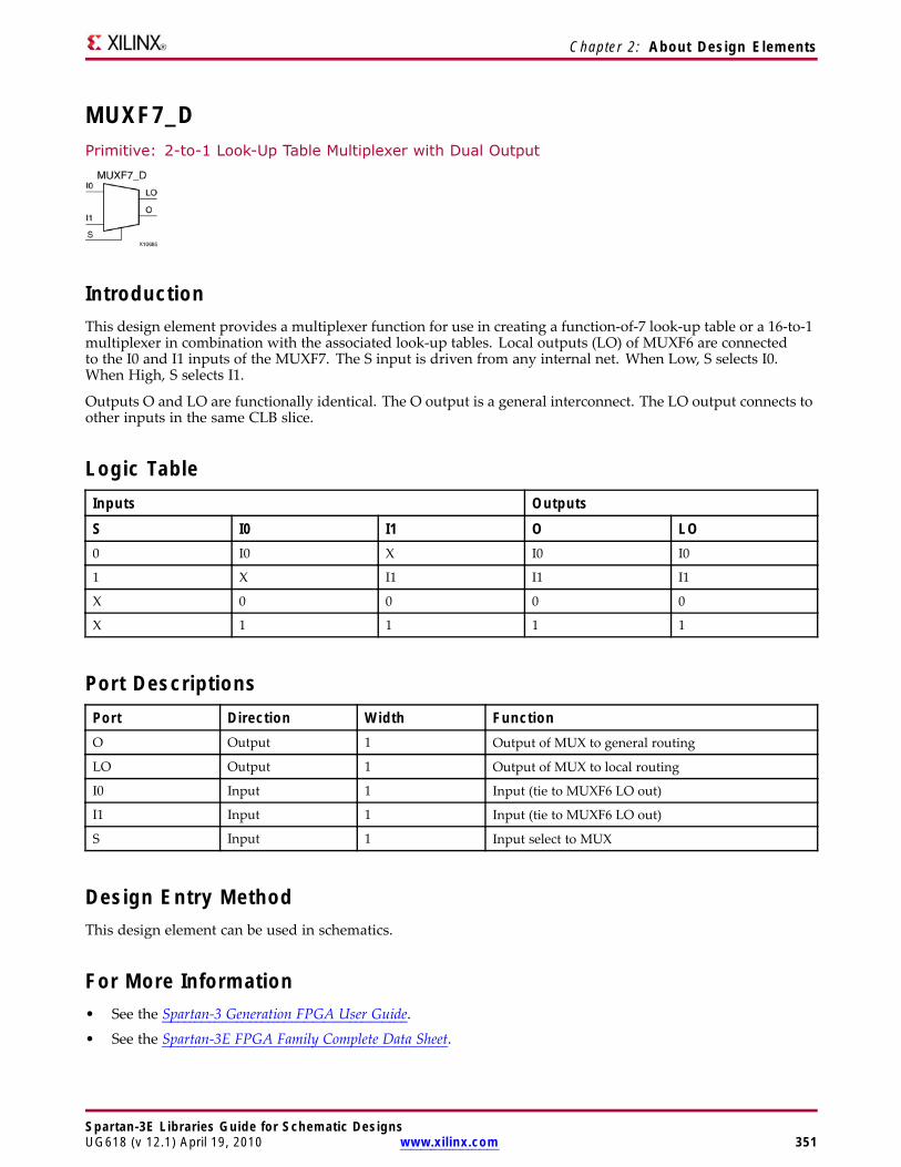
Chapter 2: About Design Elements
MUXF7_DPrimitive: 2-to-1 Look-Up Table Multiplexer with Dual Output
IntroductionThis design element provides a multiplexer function for use in creating a function-of-7 look-up table or a 16-to-1multiplexer in combination with the associated look-up tables. Local outputs (LO) of MUXF6 are connectedto the I0 and I1 inputs of the MUXF7. The S input is driven from any internal net. When Low, S selects I0.When High, S selects I1.
Outputs O and LO are functionally identical. The O output is a general interconnect. The LO output connects toother inputs in the same CLB slice.
Logic TableInputs Outputs
S I0 I1 O LO0 I0 X I0 I0
1 X I1 I1 I1
X 0 0 0 0
X 1 1 1 1
Port DescriptionsPort Direction Width FunctionO Output 1 Output of MUX to general routing
LO Output 1 Output of MUX to local routing
I0 Input 1 Input (tie to MUXF6 LO out)
I1 Input 1 Input (tie to MUXF6 LO out)
S Input 1 Input select to MUX
Design Entry MethodThis design element can be used in schematics.
For More Information• See the Spartan-3 Generation FPGA User Guide.
• See the Spartan-3E FPGA Family Complete Data Sheet.
Spartan-3E Libraries Guide for Schematic DesignsUG618 (v 12.1) April 19, 2010 www.xilinx.com 351
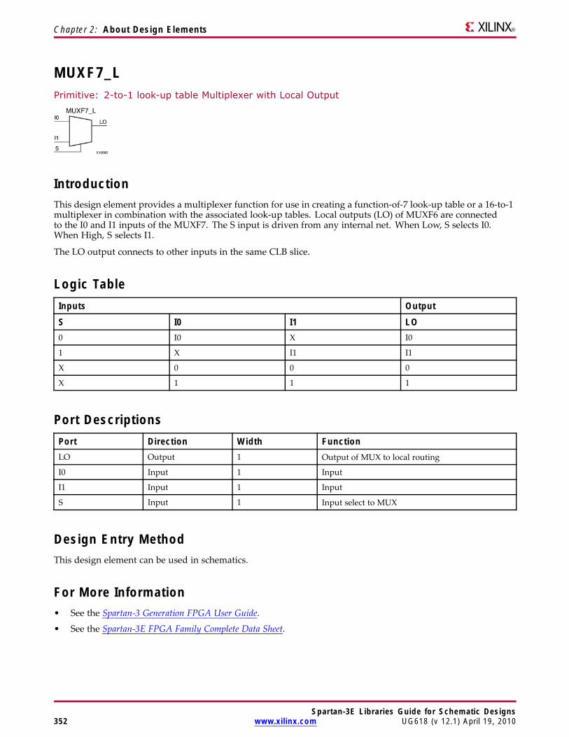
Chapter 2: About Design Elements
MUXF7_LPrimitive: 2-to-1 look-up table Multiplexer with Local Output
IntroductionThis design element provides a multiplexer function for use in creating a function-of-7 look-up table or a 16-to-1multiplexer in combination with the associated look-up tables. Local outputs (LO) of MUXF6 are connectedto the I0 and I1 inputs of the MUXF7. The S input is driven from any internal net. When Low, S selects I0.When High, S selects I1.
The LO output connects to other inputs in the same CLB slice.
Logic TableInputs Output
S I0 I1 LO0 I0 X I0
1 X I1 I1
X 0 0 0
X 1 1 1
Port DescriptionsPort Direction Width FunctionLO Output 1 Output of MUX to local routing
I0 Input 1 Input
I1 Input 1 Input
S Input 1 Input select to MUX
Design Entry MethodThis design element can be used in schematics.
For More Information• See the Spartan-3 Generation FPGA User Guide.
• See the Spartan-3E FPGA Family Complete Data Sheet.
Spartan-3E Libraries Guide for Schematic Designs352 www.xilinx.com UG618 (v 12.1) April 19, 2010
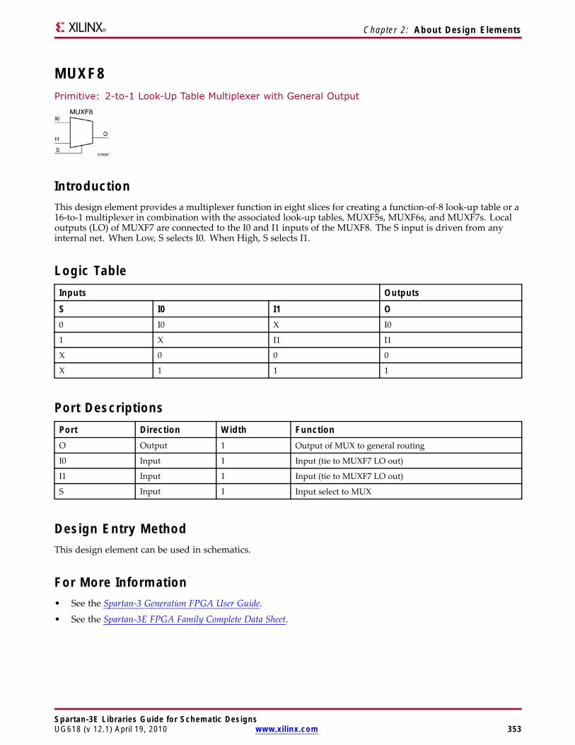
Chapter 2: About Design Elements
MUXF8Primitive: 2-to-1 Look-Up Table Multiplexer with General Output
IntroductionThis design element provides a multiplexer function in eight slices for creating a function-of-8 look-up table or a16-to-1 multiplexer in combination with the associated look-up tables, MUXF5s, MUXF6s, and MUXF7s. Localoutputs (LO) of MUXF7 are connected to the I0 and I1 inputs of the MUXF8. The S input is driven from anyinternal net. When Low, S selects I0. When High, S selects I1.
Logic TableInputs Outputs
S I0 I1 O0 I0 X I0
1 X I1 I1
X 0 0 0
X 1 1 1
Port DescriptionsPort Direction Width FunctionO Output 1 Output of MUX to general routing
I0 Input 1 Input (tie to MUXF7 LO out)
I1 Input 1 Input (tie to MUXF7 LO out)
S Input 1 Input select to MUX
Design Entry MethodThis design element can be used in schematics.
For More Information• See the Spartan-3 Generation FPGA User Guide.
• See the Spartan-3E FPGA Family Complete Data Sheet.
Spartan-3E Libraries Guide for Schematic DesignsUG618 (v 12.1) April 19, 2010 www.xilinx.com 353
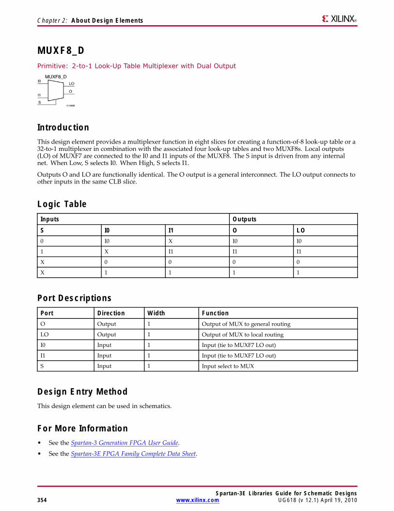
Chapter 2: About Design Elements
MUXF8_DPrimitive: 2-to-1 Look-Up Table Multiplexer with Dual Output
IntroductionThis design element provides a multiplexer function in eight slices for creating a function-of-8 look-up table or a32-to-1 multiplexer in combination with the associated four look-up tables and two MUXF8s. Local outputs(LO) of MUXF7 are connected to the I0 and I1 inputs of the MUXF8. The S input is driven from any internalnet. When Low, S selects I0. When High, S selects I1.
Outputs O and LO are functionally identical. The O output is a general interconnect. The LO output connects toother inputs in the same CLB slice.
Logic TableInputs Outputs
S I0 I1 O LO0 I0 X I0 I0
1 X I1 I1 I1
X 0 0 0 0
X 1 1 1 1
Port DescriptionsPort Direction Width FunctionO Output 1 Output of MUX to general routing
LO Output 1 Output of MUX to local routing
I0 Input 1 Input (tie to MUXF7 LO out)
I1 Input 1 Input (tie to MUXF7 LO out)
S Input 1 Input select to MUX
Design Entry MethodThis design element can be used in schematics.
For More Information• See the Spartan-3 Generation FPGA User Guide.
• See the Spartan-3E FPGA Family Complete Data Sheet.
Spartan-3E Libraries Guide for Schematic Designs354 www.xilinx.com UG618 (v 12.1) April 19, 2010
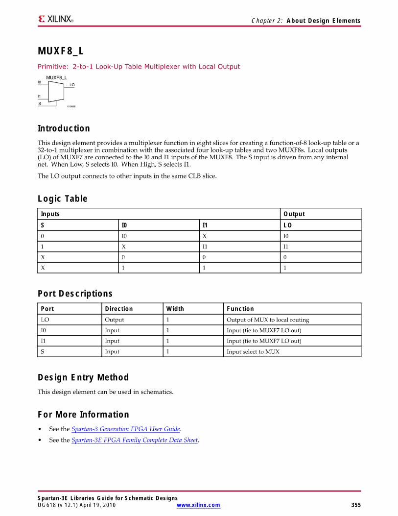
Chapter 2: About Design Elements
MUXF8_LPrimitive: 2-to-1 Look-Up Table Multiplexer with Local Output
IntroductionThis design element provides a multiplexer function in eight slices for creating a function-of-8 look-up table or a32-to-1 multiplexer in combination with the associated four look-up tables and two MUXF8s. Local outputs(LO) of MUXF7 are connected to the I0 and I1 inputs of the MUXF8. The S input is driven from any internalnet. When Low, S selects I0. When High, S selects I1.
The LO output connects to other inputs in the same CLB slice.
Logic TableInputs Output
S I0 I1 LO0 I0 X I0
1 X I1 I1
X 0 0 0
X 1 1 1
Port DescriptionsPort Direction Width FunctionLO Output 1 Output of MUX to local routing
I0 Input 1 Input (tie to MUXF7 LO out)
I1 Input 1 Input (tie to MUXF7 LO out)
S Input 1 Input select to MUX
Design Entry MethodThis design element can be used in schematics.
For More Information• See the Spartan-3 Generation FPGA User Guide.
• See the Spartan-3E FPGA Family Complete Data Sheet.
Spartan-3E Libraries Guide for Schematic DesignsUG618 (v 12.1) April 19, 2010 www.xilinx.com 355
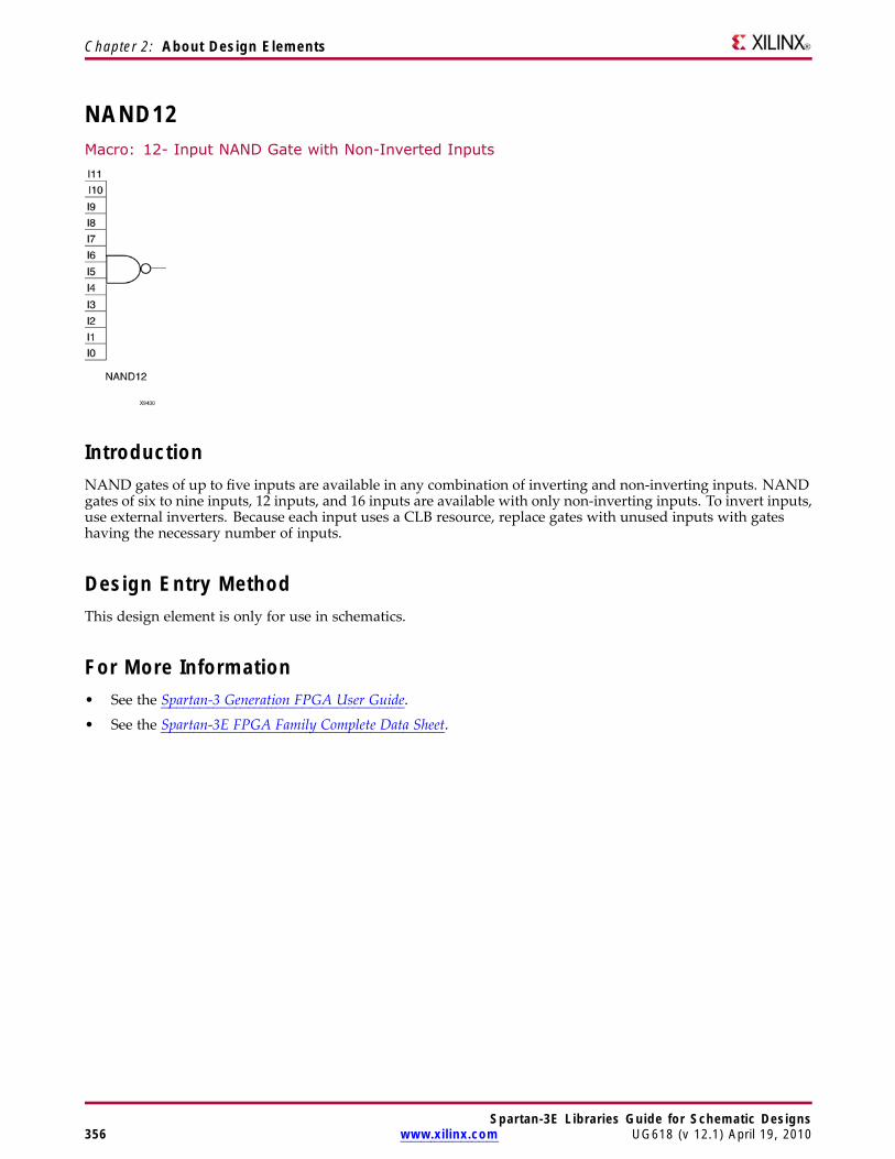
Chapter 2: About Design Elements
NAND12Macro: 12- Input NAND Gate with Non-Inverted Inputs
IntroductionNAND gates of up to five inputs are available in any combination of inverting and non-inverting inputs. NANDgates of six to nine inputs, 12 inputs, and 16 inputs are available with only non-inverting inputs. To invert inputs,use external inverters. Because each input uses a CLB resource, replace gates with unused inputs with gateshaving the necessary number of inputs.
Design Entry MethodThis design element is only for use in schematics.
For More Information• See the Spartan-3 Generation FPGA User Guide.
• See the Spartan-3E FPGA Family Complete Data Sheet.
Spartan-3E Libraries Guide for Schematic Designs356 www.xilinx.com UG618 (v 12.1) April 19, 2010
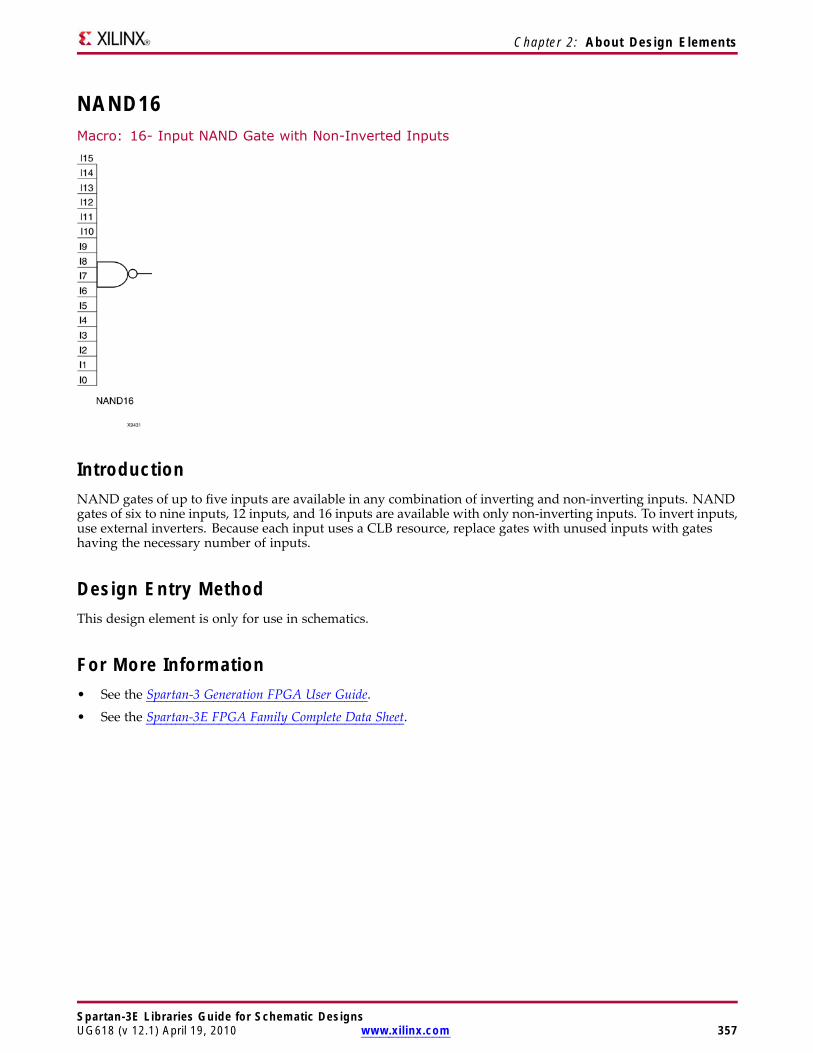
Chapter 2: About Design Elements
NAND16Macro: 16- Input NAND Gate with Non-Inverted Inputs
IntroductionNAND gates of up to five inputs are available in any combination of inverting and non-inverting inputs. NANDgates of six to nine inputs, 12 inputs, and 16 inputs are available with only non-inverting inputs. To invert inputs,use external inverters. Because each input uses a CLB resource, replace gates with unused inputs with gateshaving the necessary number of inputs.
Design Entry MethodThis design element is only for use in schematics.
For More Information• See the Spartan-3 Generation FPGA User Guide.
• See the Spartan-3E FPGA Family Complete Data Sheet.
Spartan-3E Libraries Guide for Schematic DesignsUG618 (v 12.1) April 19, 2010 www.xilinx.com 357
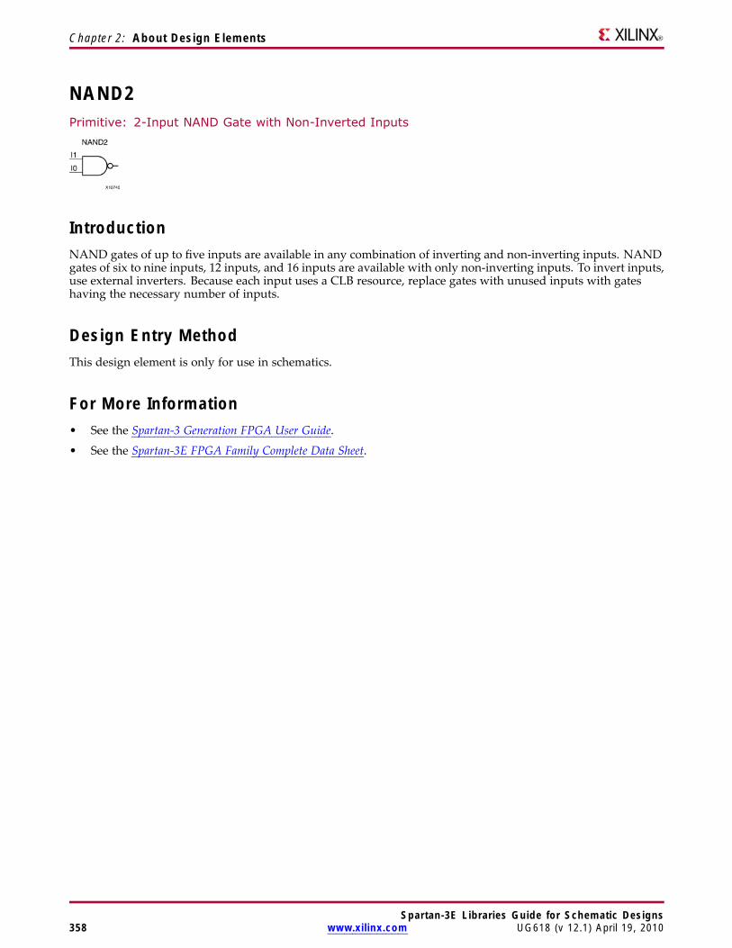
Chapter 2: About Design Elements
NAND2Primitive: 2-Input NAND Gate with Non-Inverted Inputs
IntroductionNAND gates of up to five inputs are available in any combination of inverting and non-inverting inputs. NANDgates of six to nine inputs, 12 inputs, and 16 inputs are available with only non-inverting inputs. To invert inputs,use external inverters. Because each input uses a CLB resource, replace gates with unused inputs with gateshaving the necessary number of inputs.
Design Entry MethodThis design element is only for use in schematics.
For More Information• See the Spartan-3 Generation FPGA User Guide.
• See the Spartan-3E FPGA Family Complete Data Sheet.
Spartan-3E Libraries Guide for Schematic Designs358 www.xilinx.com UG618 (v 12.1) April 19, 2010
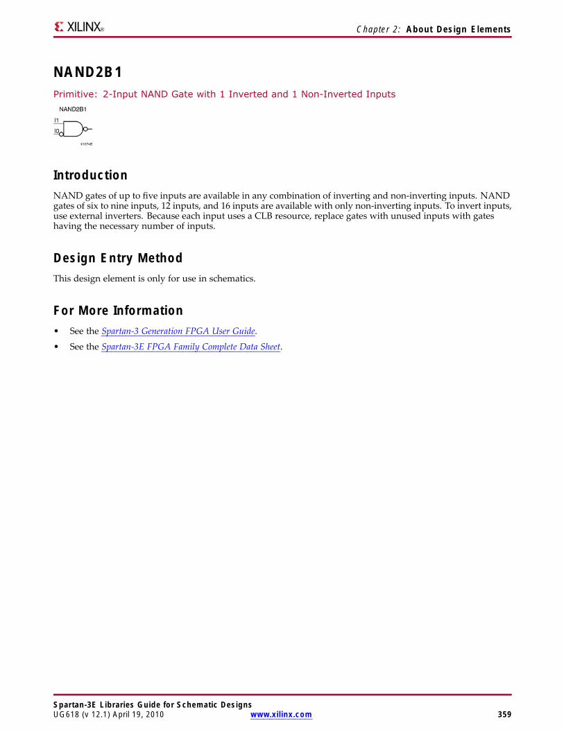
Chapter 2: About Design Elements
NAND2B1Primitive: 2-Input NAND Gate with 1 Inverted and 1 Non-Inverted Inputs
IntroductionNAND gates of up to five inputs are available in any combination of inverting and non-inverting inputs. NANDgates of six to nine inputs, 12 inputs, and 16 inputs are available with only non-inverting inputs. To invert inputs,use external inverters. Because each input uses a CLB resource, replace gates with unused inputs with gateshaving the necessary number of inputs.
Design Entry MethodThis design element is only for use in schematics.
For More Information• See the Spartan-3 Generation FPGA User Guide.
• See the Spartan-3E FPGA Family Complete Data Sheet.
Spartan-3E Libraries Guide for Schematic DesignsUG618 (v 12.1) April 19, 2010 www.xilinx.com 359
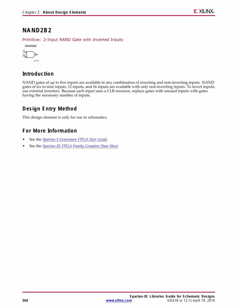
Chapter 2: About Design Elements
NAND2B2Primitive: 2-Input NAND Gate with Inverted Inputs
IntroductionNAND gates of up to five inputs are available in any combination of inverting and non-inverting inputs. NANDgates of six to nine inputs, 12 inputs, and 16 inputs are available with only non-inverting inputs. To invert inputs,use external inverters. Because each input uses a CLB resource, replace gates with unused inputs with gateshaving the necessary number of inputs.
Design Entry MethodThis design element is only for use in schematics.
For More Information• See the Spartan-3 Generation FPGA User Guide.
• See the Spartan-3E FPGA Family Complete Data Sheet.
Spartan-3E Libraries Guide for Schematic Designs360 www.xilinx.com UG618 (v 12.1) April 19, 2010
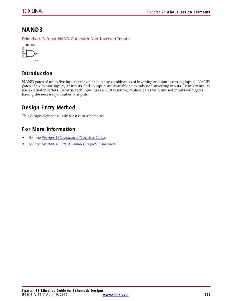
Chapter 2: About Design Elements
NAND3Primitive: 3-Input NAND Gate with Non-Inverted Inputs
IntroductionNAND gates of up to five inputs are available in any combination of inverting and non-inverting inputs. NANDgates of six to nine inputs, 12 inputs, and 16 inputs are available with only non-inverting inputs. To invert inputs,use external inverters. Because each input uses a CLB resource, replace gates with unused inputs with gateshaving the necessary number of inputs.
Design Entry MethodThis design element is only for use in schematics.
For More Information• See the Spartan-3 Generation FPGA User Guide.
• See the Spartan-3E FPGA Family Complete Data Sheet.
Spartan-3E Libraries Guide for Schematic DesignsUG618 (v 12.1) April 19, 2010 www.xilinx.com 361

Chapter 2: About Design Elements
NAND3B1Primitive: 3-Input NAND Gate with 1 Inverted and 2 Non-Inverted Inputs
IntroductionNAND gates of up to five inputs are available in any combination of inverting and non-inverting inputs. NANDgates of six to nine inputs, 12 inputs, and 16 inputs are available with only non-inverting inputs. To invert inputs,use external inverters. Because each input uses a CLB resource, replace gates with unused inputs with gateshaving the necessary number of inputs.
Design Entry MethodThis design element is only for use in schematics.
For More Information• See the Spartan-3 Generation FPGA User Guide.
• See the Spartan-3E FPGA Family Complete Data Sheet.
Spartan-3E Libraries Guide for Schematic Designs362 www.xilinx.com UG618 (v 12.1) April 19, 2010
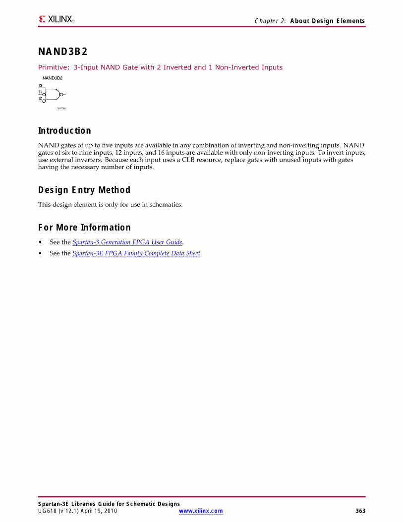
Chapter 2: About Design Elements
NAND3B2Primitive: 3-Input NAND Gate with 2 Inverted and 1 Non-Inverted Inputs
IntroductionNAND gates of up to five inputs are available in any combination of inverting and non-inverting inputs. NANDgates of six to nine inputs, 12 inputs, and 16 inputs are available with only non-inverting inputs. To invert inputs,use external inverters. Because each input uses a CLB resource, replace gates with unused inputs with gateshaving the necessary number of inputs.
Design Entry MethodThis design element is only for use in schematics.
For More Information• See the Spartan-3 Generation FPGA User Guide.
• See the Spartan-3E FPGA Family Complete Data Sheet.
Spartan-3E Libraries Guide for Schematic DesignsUG618 (v 12.1) April 19, 2010 www.xilinx.com 363
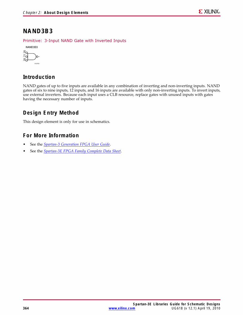
Chapter 2: About Design Elements
NAND3B3Primitive: 3-Input NAND Gate with Inverted Inputs
IntroductionNAND gates of up to five inputs are available in any combination of inverting and non-inverting inputs. NANDgates of six to nine inputs, 12 inputs, and 16 inputs are available with only non-inverting inputs. To invert inputs,use external inverters. Because each input uses a CLB resource, replace gates with unused inputs with gateshaving the necessary number of inputs.
Design Entry MethodThis design element is only for use in schematics.
For More Information• See the Spartan-3 Generation FPGA User Guide.
• See the Spartan-3E FPGA Family Complete Data Sheet.
Spartan-3E Libraries Guide for Schematic Designs364 www.xilinx.com UG618 (v 12.1) April 19, 2010
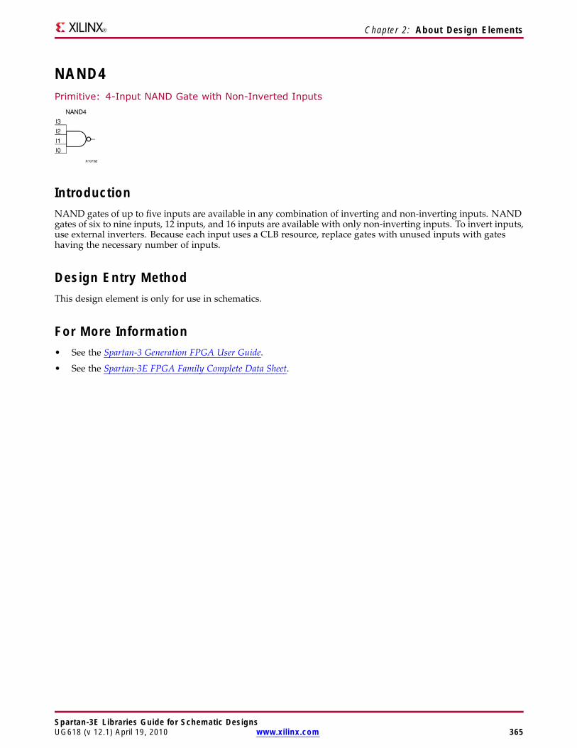
Chapter 2: About Design Elements
NAND4Primitive: 4-Input NAND Gate with Non-Inverted Inputs
IntroductionNAND gates of up to five inputs are available in any combination of inverting and non-inverting inputs. NANDgates of six to nine inputs, 12 inputs, and 16 inputs are available with only non-inverting inputs. To invert inputs,use external inverters. Because each input uses a CLB resource, replace gates with unused inputs with gateshaving the necessary number of inputs.
Design Entry MethodThis design element is only for use in schematics.
For More Information• See the Spartan-3 Generation FPGA User Guide.
• See the Spartan-3E FPGA Family Complete Data Sheet.
Spartan-3E Libraries Guide for Schematic DesignsUG618 (v 12.1) April 19, 2010 www.xilinx.com 365
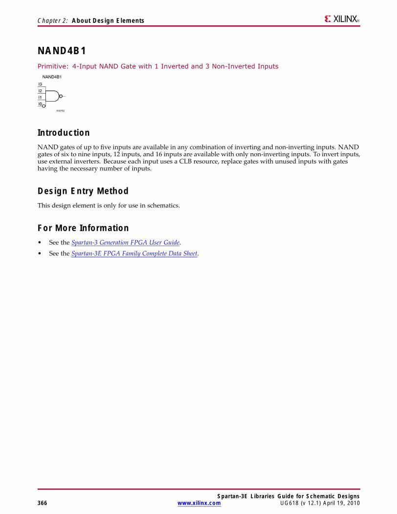
Chapter 2: About Design Elements
NAND4B1Primitive: 4-Input NAND Gate with 1 Inverted and 3 Non-Inverted Inputs
IntroductionNAND gates of up to five inputs are available in any combination of inverting and non-inverting inputs. NANDgates of six to nine inputs, 12 inputs, and 16 inputs are available with only non-inverting inputs. To invert inputs,use external inverters. Because each input uses a CLB resource, replace gates with unused inputs with gateshaving the necessary number of inputs.
Design Entry MethodThis design element is only for use in schematics.
For More Information• See the Spartan-3 Generation FPGA User Guide.
• See the Spartan-3E FPGA Family Complete Data Sheet.
Spartan-3E Libraries Guide for Schematic Designs366 www.xilinx.com UG618 (v 12.1) April 19, 2010
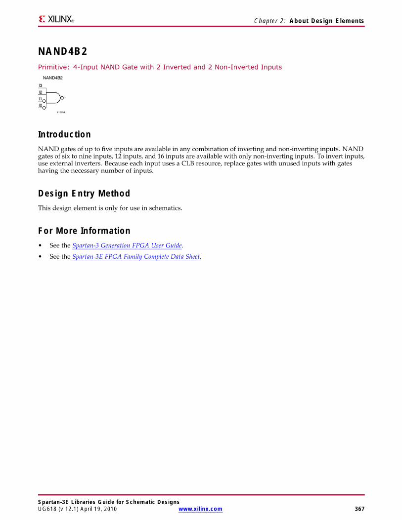
Chapter 2: About Design Elements
NAND4B2Primitive: 4-Input NAND Gate with 2 Inverted and 2 Non-Inverted Inputs
IntroductionNAND gates of up to five inputs are available in any combination of inverting and non-inverting inputs. NANDgates of six to nine inputs, 12 inputs, and 16 inputs are available with only non-inverting inputs. To invert inputs,use external inverters. Because each input uses a CLB resource, replace gates with unused inputs with gateshaving the necessary number of inputs.
Design Entry MethodThis design element is only for use in schematics.
For More Information• See the Spartan-3 Generation FPGA User Guide.
• See the Spartan-3E FPGA Family Complete Data Sheet.
Spartan-3E Libraries Guide for Schematic DesignsUG618 (v 12.1) April 19, 2010 www.xilinx.com 367

Chapter 2: About Design Elements
NAND4B3Primitive: 4-Input NAND Gate with 3 Inverted and 1 Non-Inverted Inputs
IntroductionNAND gates of up to five inputs are available in any combination of inverting and non-inverting inputs. NANDgates of six to nine inputs, 12 inputs, and 16 inputs are available with only non-inverting inputs. To invert inputs,use external inverters. Because each input uses a CLB resource, replace gates with unused inputs with gateshaving the necessary number of inputs.
Design Entry MethodThis design element is only for use in schematics.
For More Information• See the Spartan-3 Generation FPGA User Guide.
• See the Spartan-3E FPGA Family Complete Data Sheet.
Spartan-3E Libraries Guide for Schematic Designs368 www.xilinx.com UG618 (v 12.1) April 19, 2010
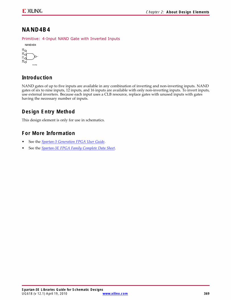
Chapter 2: About Design Elements
NAND4B4Primitive: 4-Input NAND Gate with Inverted Inputs
IntroductionNAND gates of up to five inputs are available in any combination of inverting and non-inverting inputs. NANDgates of six to nine inputs, 12 inputs, and 16 inputs are available with only non-inverting inputs. To invert inputs,use external inverters. Because each input uses a CLB resource, replace gates with unused inputs with gateshaving the necessary number of inputs.
Design Entry MethodThis design element is only for use in schematics.
For More Information• See the Spartan-3 Generation FPGA User Guide.
• See the Spartan-3E FPGA Family Complete Data Sheet.
Spartan-3E Libraries Guide for Schematic DesignsUG618 (v 12.1) April 19, 2010 www.xilinx.com 369
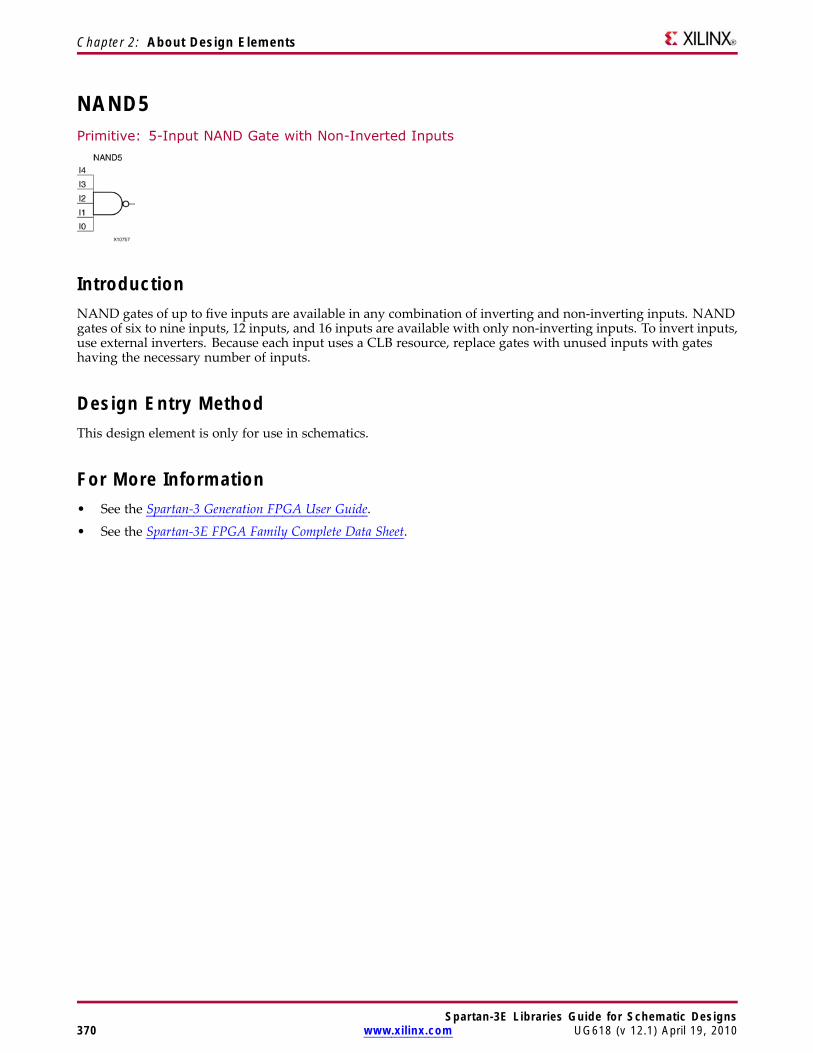
Chapter 2: About Design Elements
NAND5Primitive: 5-Input NAND Gate with Non-Inverted Inputs
IntroductionNAND gates of up to five inputs are available in any combination of inverting and non-inverting inputs. NANDgates of six to nine inputs, 12 inputs, and 16 inputs are available with only non-inverting inputs. To invert inputs,use external inverters. Because each input uses a CLB resource, replace gates with unused inputs with gateshaving the necessary number of inputs.
Design Entry MethodThis design element is only for use in schematics.
For More Information• See the Spartan-3 Generation FPGA User Guide.
• See the Spartan-3E FPGA Family Complete Data Sheet.
Spartan-3E Libraries Guide for Schematic Designs370 www.xilinx.com UG618 (v 12.1) April 19, 2010

Chapter 2: About Design Elements
NAND5B1Primitive: 5-Input NAND Gate with 1 Inverted and 4 Non-Inverted Inputs
IntroductionNAND gates of up to five inputs are available in any combination of inverting and non-inverting inputs. NANDgates of six to nine inputs, 12 inputs, and 16 inputs are available with only non-inverting inputs. To invert inputs,use external inverters. Because each input uses a CLB resource, replace gates with unused inputs with gateshaving the necessary number of inputs.
Design Entry MethodThis design element is only for use in schematics.
For More Information• See the Spartan-3 Generation FPGA User Guide.
• See the Spartan-3E FPGA Family Complete Data Sheet.
Spartan-3E Libraries Guide for Schematic DesignsUG618 (v 12.1) April 19, 2010 www.xilinx.com 371

Chapter 2: About Design Elements
NAND5B2Primitive: 5-Input NAND Gate with 2 Inverted and 3 Non-Inverted Inputs
IntroductionNAND gates of up to five inputs are available in any combination of inverting and non-inverting inputs. NANDgates of six to nine inputs, 12 inputs, and 16 inputs are available with only non-inverting inputs. To invert inputs,use external inverters. Because each input uses a CLB resource, replace gates with unused inputs with gateshaving the necessary number of inputs.
Design Entry MethodThis design element is only for use in schematics.
For More Information• See the Spartan-3 Generation FPGA User Guide.
• See the Spartan-3E FPGA Family Complete Data Sheet.
Spartan-3E Libraries Guide for Schematic Designs372 www.xilinx.com UG618 (v 12.1) April 19, 2010
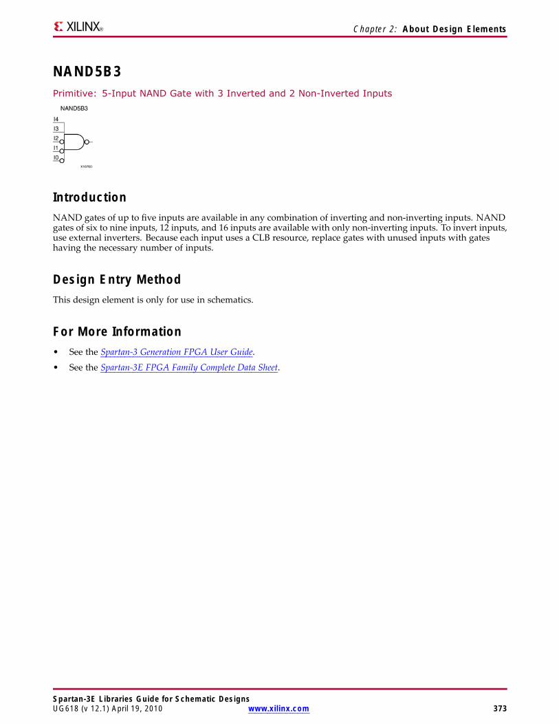
Chapter 2: About Design Elements
NAND5B3Primitive: 5-Input NAND Gate with 3 Inverted and 2 Non-Inverted Inputs
IntroductionNAND gates of up to five inputs are available in any combination of inverting and non-inverting inputs. NANDgates of six to nine inputs, 12 inputs, and 16 inputs are available with only non-inverting inputs. To invert inputs,use external inverters. Because each input uses a CLB resource, replace gates with unused inputs with gateshaving the necessary number of inputs.
Design Entry MethodThis design element is only for use in schematics.
For More Information• See the Spartan-3 Generation FPGA User Guide.
• See the Spartan-3E FPGA Family Complete Data Sheet.
Spartan-3E Libraries Guide for Schematic DesignsUG618 (v 12.1) April 19, 2010 www.xilinx.com 373

Chapter 2: About Design Elements
NAND5B4Primitive: 5-Input NAND Gate with 4 Inverted and 1 Non-Inverted Inputs
IntroductionNAND gates of up to five inputs are available in any combination of inverting and non-inverting inputs. NANDgates of six to nine inputs, 12 inputs, and 16 inputs are available with only non-inverting inputs. To invert inputs,use external inverters. Because each input uses a CLB resource, replace gates with unused inputs with gateshaving the necessary number of inputs.
Design Entry MethodThis design element is only for use in schematics.
For More Information• See the Spartan-3 Generation FPGA User Guide.
• See the Spartan-3E FPGA Family Complete Data Sheet.
Spartan-3E Libraries Guide for Schematic Designs374 www.xilinx.com UG618 (v 12.1) April 19, 2010
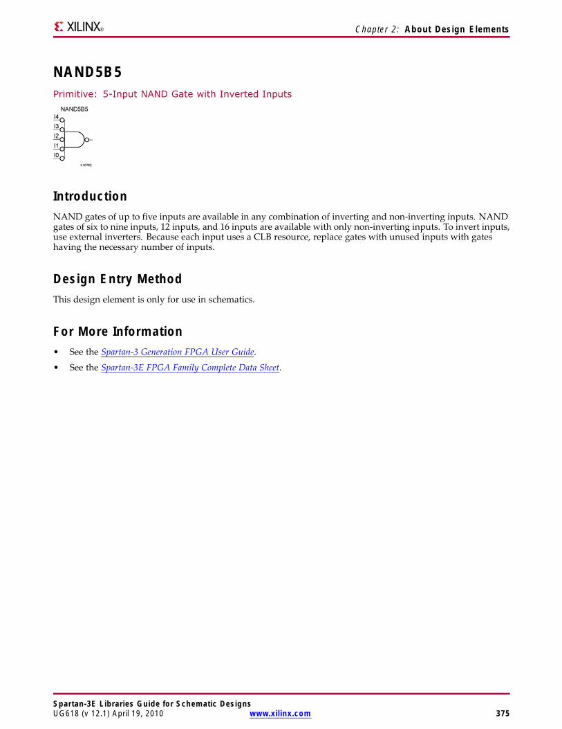
Chapter 2: About Design Elements
NAND5B5Primitive: 5-Input NAND Gate with Inverted Inputs
IntroductionNAND gates of up to five inputs are available in any combination of inverting and non-inverting inputs. NANDgates of six to nine inputs, 12 inputs, and 16 inputs are available with only non-inverting inputs. To invert inputs,use external inverters. Because each input uses a CLB resource, replace gates with unused inputs with gateshaving the necessary number of inputs.
Design Entry MethodThis design element is only for use in schematics.
For More Information• See the Spartan-3 Generation FPGA User Guide.
• See the Spartan-3E FPGA Family Complete Data Sheet.
Spartan-3E Libraries Guide for Schematic DesignsUG618 (v 12.1) April 19, 2010 www.xilinx.com 375

Chapter 2: About Design Elements
NAND6Macro: 6-Input NAND Gate with Non-Inverted Inputs
IntroductionNAND gates of up to five inputs are available in any combination of inverting and non-inverting inputs. NANDgates of six to nine inputs, 12 inputs, and 16 inputs are available with only non-inverting inputs. To invert inputs,use external inverters. Because each input uses a CLB resource, replace gates with unused inputs with gateshaving the necessary number of inputs.
Design Entry MethodThis design element is only for use in schematics.
For More Information• See the Spartan-3 Generation FPGA User Guide.
• See the Spartan-3E FPGA Family Complete Data Sheet.
Spartan-3E Libraries Guide for Schematic Designs376 www.xilinx.com UG618 (v 12.1) April 19, 2010
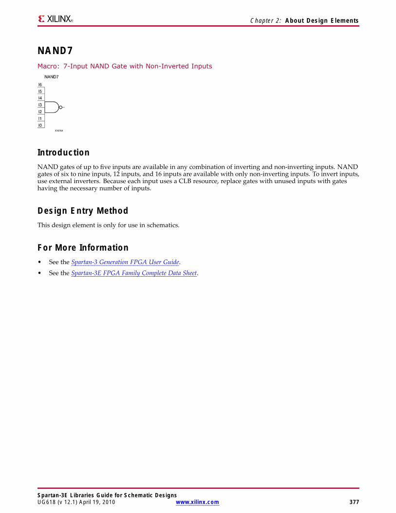
Chapter 2: About Design Elements
NAND7Macro: 7-Input NAND Gate with Non-Inverted Inputs
IntroductionNAND gates of up to five inputs are available in any combination of inverting and non-inverting inputs. NANDgates of six to nine inputs, 12 inputs, and 16 inputs are available with only non-inverting inputs. To invert inputs,use external inverters. Because each input uses a CLB resource, replace gates with unused inputs with gateshaving the necessary number of inputs.
Design Entry MethodThis design element is only for use in schematics.
For More Information• See the Spartan-3 Generation FPGA User Guide.
• See the Spartan-3E FPGA Family Complete Data Sheet.
Spartan-3E Libraries Guide for Schematic DesignsUG618 (v 12.1) April 19, 2010 www.xilinx.com 377
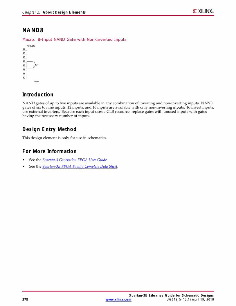
Chapter 2: About Design Elements
NAND8Macro: 8-Input NAND Gate with Non-Inverted Inputs
IntroductionNAND gates of up to five inputs are available in any combination of inverting and non-inverting inputs. NANDgates of six to nine inputs, 12 inputs, and 16 inputs are available with only non-inverting inputs. To invert inputs,use external inverters. Because each input uses a CLB resource, replace gates with unused inputs with gateshaving the necessary number of inputs.
Design Entry MethodThis design element is only for use in schematics.
For More Information• See the Spartan-3 Generation FPGA User Guide.
• See the Spartan-3E FPGA Family Complete Data Sheet.
Spartan-3E Libraries Guide for Schematic Designs378 www.xilinx.com UG618 (v 12.1) April 19, 2010
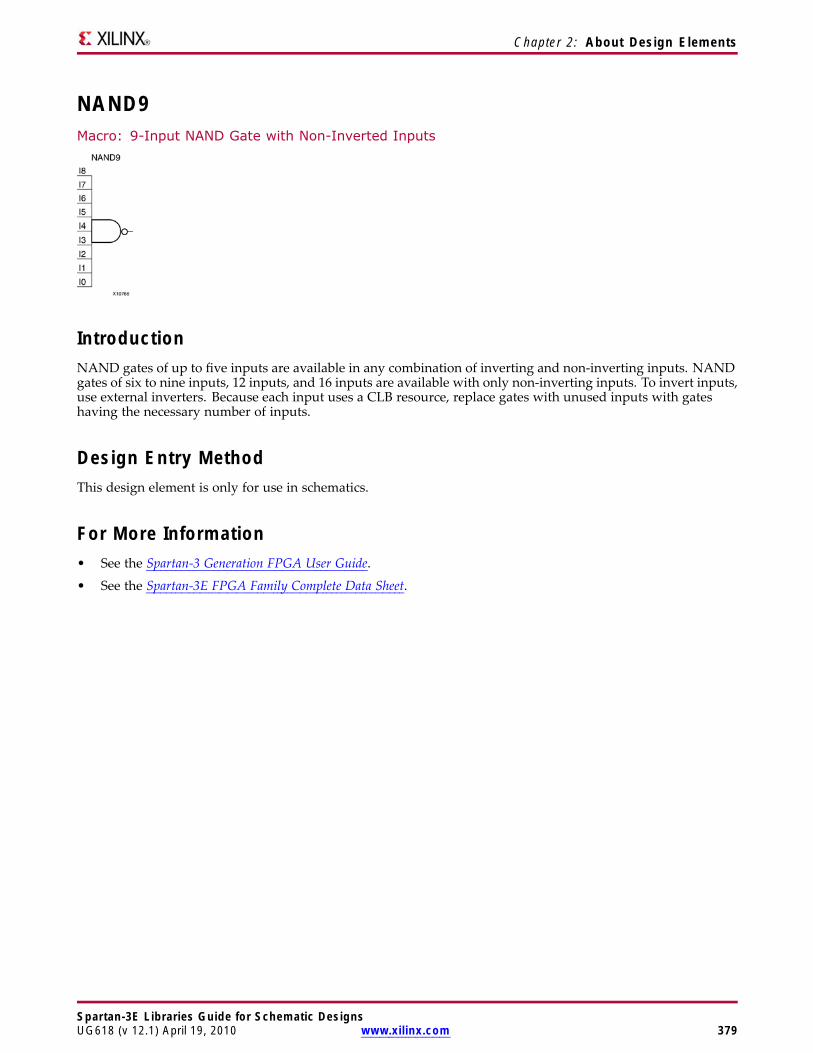
Chapter 2: About Design Elements
NAND9Macro: 9-Input NAND Gate with Non-Inverted Inputs
IntroductionNAND gates of up to five inputs are available in any combination of inverting and non-inverting inputs. NANDgates of six to nine inputs, 12 inputs, and 16 inputs are available with only non-inverting inputs. To invert inputs,use external inverters. Because each input uses a CLB resource, replace gates with unused inputs with gateshaving the necessary number of inputs.
Design Entry MethodThis design element is only for use in schematics.
For More Information• See the Spartan-3 Generation FPGA User Guide.
• See the Spartan-3E FPGA Family Complete Data Sheet.
Spartan-3E Libraries Guide for Schematic DesignsUG618 (v 12.1) April 19, 2010 www.xilinx.com 379
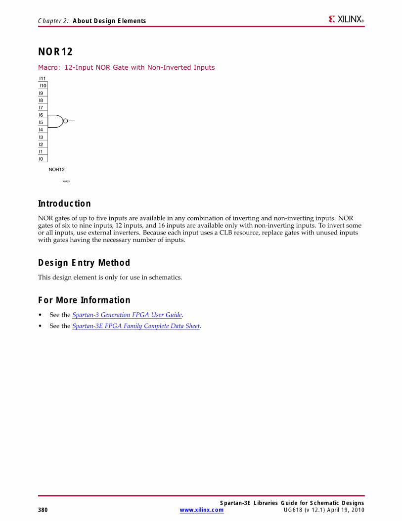
Chapter 2: About Design Elements
NOR12Macro: 12-Input NOR Gate with Non-Inverted Inputs
IntroductionNOR gates of up to five inputs are available in any combination of inverting and non-inverting inputs. NORgates of six to nine inputs, 12 inputs, and 16 inputs are available only with non-inverting inputs. To invert someor all inputs, use external inverters. Because each input uses a CLB resource, replace gates with unused inputswith gates having the necessary number of inputs.
Design Entry MethodThis design element is only for use in schematics.
For More Information• See the Spartan-3 Generation FPGA User Guide.
• See the Spartan-3E FPGA Family Complete Data Sheet.
Spartan-3E Libraries Guide for Schematic Designs380 www.xilinx.com UG618 (v 12.1) April 19, 2010
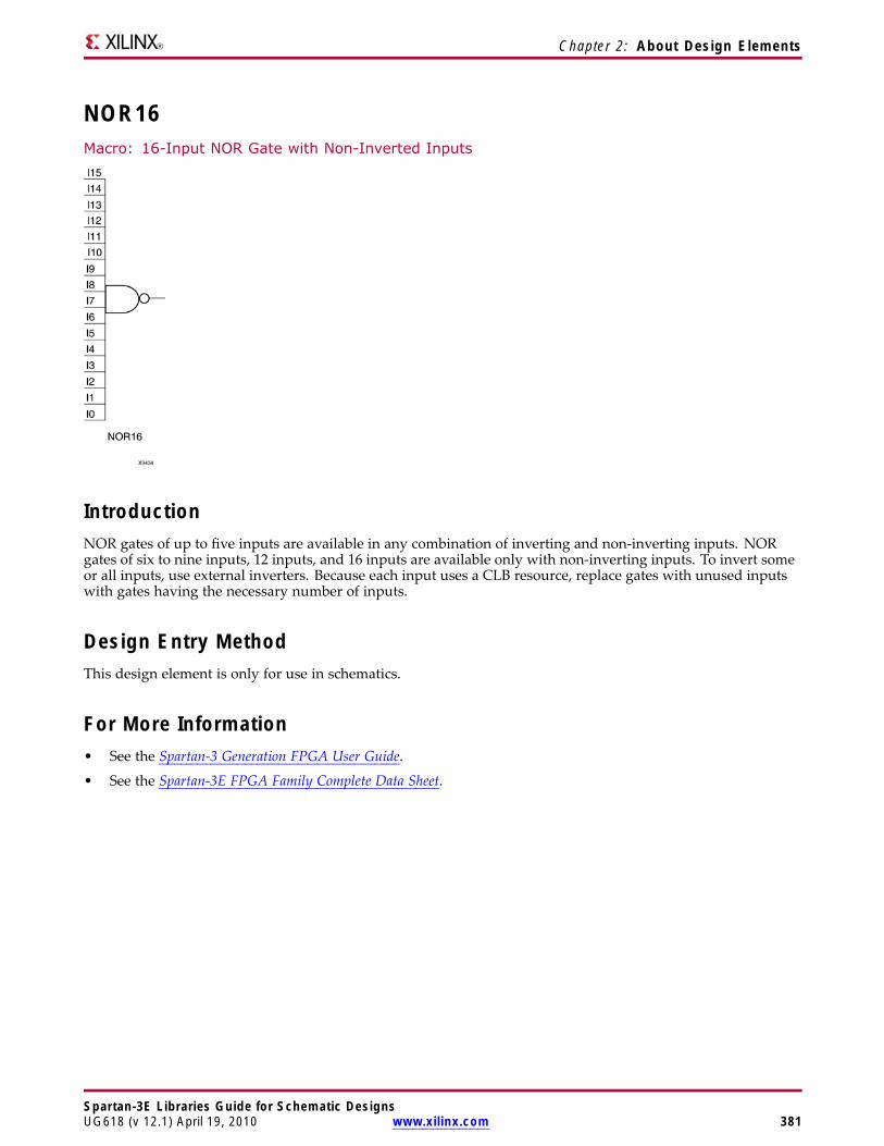
Chapter 2: About Design Elements
NOR16Macro: 16-Input NOR Gate with Non-Inverted Inputs
IntroductionNOR gates of up to five inputs are available in any combination of inverting and non-inverting inputs. NORgates of six to nine inputs, 12 inputs, and 16 inputs are available only with non-inverting inputs. To invert someor all inputs, use external inverters. Because each input uses a CLB resource, replace gates with unused inputswith gates having the necessary number of inputs.
Design Entry MethodThis design element is only for use in schematics.
For More Information• See the Spartan-3 Generation FPGA User Guide.
• See the Spartan-3E FPGA Family Complete Data Sheet.
Spartan-3E Libraries Guide for Schematic DesignsUG618 (v 12.1) April 19, 2010 www.xilinx.com 381

Chapter 2: About Design Elements
NOR2Primitive: 2-Input NOR Gate with Non-Inverted Inputs
IntroductionNOR gates of up to five inputs are available in any combination of inverting and non-inverting inputs. NORgates of six to nine inputs, 12 inputs, and 16 inputs are available only with non-inverting inputs. To invert someor all inputs, use external inverters. Because each input uses a CLB resource, replace gates with unused inputswith gates having the necessary number of inputs.
Design Entry MethodThis design element is only for use in schematics.
For More Information• See the Spartan-3 Generation FPGA User Guide.
• See the Spartan-3E FPGA Family Complete Data Sheet.
Spartan-3E Libraries Guide for Schematic Designs382 www.xilinx.com UG618 (v 12.1) April 19, 2010
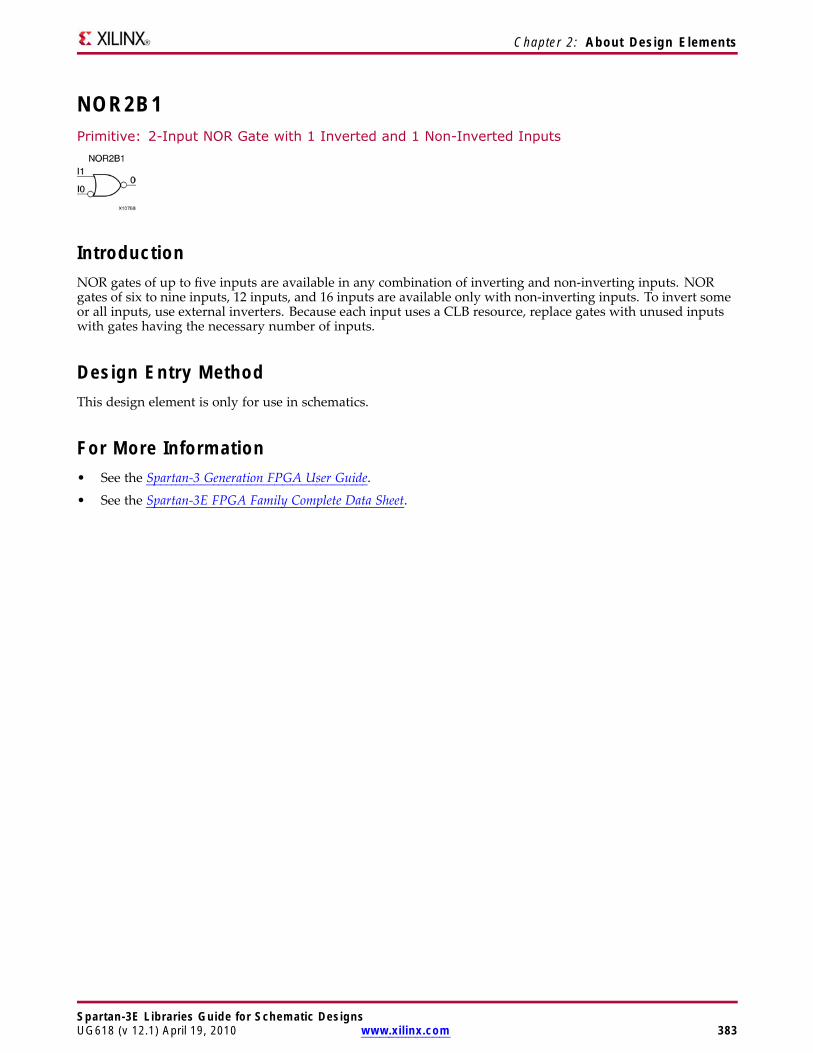
Chapter 2: About Design Elements
NOR2B1Primitive: 2-Input NOR Gate with 1 Inverted and 1 Non-Inverted Inputs
IntroductionNOR gates of up to five inputs are available in any combination of inverting and non-inverting inputs. NORgates of six to nine inputs, 12 inputs, and 16 inputs are available only with non-inverting inputs. To invert someor all inputs, use external inverters. Because each input uses a CLB resource, replace gates with unused inputswith gates having the necessary number of inputs.
Design Entry MethodThis design element is only for use in schematics.
For More Information• See the Spartan-3 Generation FPGA User Guide.
• See the Spartan-3E FPGA Family Complete Data Sheet.
Spartan-3E Libraries Guide for Schematic DesignsUG618 (v 12.1) April 19, 2010 www.xilinx.com 383

Chapter 2: About Design Elements
NOR2B2Primitive: 2-Input NOR Gate with Inverted Inputs
IntroductionNOR gates of up to five inputs are available in any combination of inverting and non-inverting inputs. NORgates of six to nine inputs, 12 inputs, and 16 inputs are available only with non-inverting inputs. To invert someor all inputs, use external inverters. Because each input uses a CLB resource, replace gates with unused inputswith gates having the necessary number of inputs.
Design Entry MethodThis design element is only for use in schematics.
For More Information• See the Spartan-3 Generation FPGA User Guide.
• See the Spartan-3E FPGA Family Complete Data Sheet.
Spartan-3E Libraries Guide for Schematic Designs384 www.xilinx.com UG618 (v 12.1) April 19, 2010

Chapter 2: About Design Elements
NOR3Primitive: 3-Input NOR Gate with Non-Inverted Inputs
IntroductionNOR gates of up to five inputs are available in any combination of inverting and non-inverting inputs. NORgates of six to nine inputs, 12 inputs, and 16 inputs are available only with non-inverting inputs. To invert someor all inputs, use external inverters. Because each input uses a CLB resource, replace gates with unused inputswith gates having the necessary number of inputs.
Design Entry MethodThis design element is only for use in schematics.
For More Information• See the Spartan-3 Generation FPGA User Guide.
• See the Spartan-3E FPGA Family Complete Data Sheet.
Spartan-3E Libraries Guide for Schematic DesignsUG618 (v 12.1) April 19, 2010 www.xilinx.com 385

Chapter 2: About Design Elements
NOR3B1Primitive: 3-Input NOR Gate with 1 Inverted and 2 Non-Inverted Inputs
IntroductionNOR gates of up to five inputs are available in any combination of inverting and non-inverting inputs. NORgates of six to nine inputs, 12 inputs, and 16 inputs are available only with non-inverting inputs. To invert someor all inputs, use external inverters. Because each input uses a CLB resource, replace gates with unused inputswith gates having the necessary number of inputs.
Design Entry MethodThis design element is only for use in schematics.
For More Information• See the Spartan-3 Generation FPGA User Guide.
• See the Spartan-3E FPGA Family Complete Data Sheet.
Spartan-3E Libraries Guide for Schematic Designs386 www.xilinx.com UG618 (v 12.1) April 19, 2010
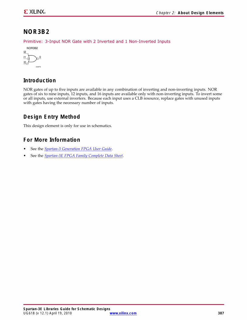
Chapter 2: About Design Elements
NOR3B2Primitive: 3-Input NOR Gate with 2 Inverted and 1 Non-Inverted Inputs
IntroductionNOR gates of up to five inputs are available in any combination of inverting and non-inverting inputs. NORgates of six to nine inputs, 12 inputs, and 16 inputs are available only with non-inverting inputs. To invert someor all inputs, use external inverters. Because each input uses a CLB resource, replace gates with unused inputswith gates having the necessary number of inputs.
Design Entry MethodThis design element is only for use in schematics.
For More Information• See the Spartan-3 Generation FPGA User Guide.
• See the Spartan-3E FPGA Family Complete Data Sheet.
Spartan-3E Libraries Guide for Schematic DesignsUG618 (v 12.1) April 19, 2010 www.xilinx.com 387

Chapter 2: About Design Elements
NOR3B3Primitive: 3-Input NOR Gate with Inverted Inputs
IntroductionNOR gates of up to five inputs are available in any combination of inverting and non-inverting inputs. NORgates of six to nine inputs, 12 inputs, and 16 inputs are available only with non-inverting inputs. To invert someor all inputs, use external inverters. Because each input uses a CLB resource, replace gates with unused inputswith gates having the necessary number of inputs.
Design Entry MethodThis design element is only for use in schematics.
For More Information• See the Spartan-3 Generation FPGA User Guide.
• See the Spartan-3E FPGA Family Complete Data Sheet.
Spartan-3E Libraries Guide for Schematic Designs388 www.xilinx.com UG618 (v 12.1) April 19, 2010

Chapter 2: About Design Elements
NOR4Primitive: 4-Input NOR Gate with Non-Inverted Inputs
IntroductionNOR gates of up to five inputs are available in any combination of inverting and non-inverting inputs. NORgates of six to nine inputs, 12 inputs, and 16 inputs are available only with non-inverting inputs. To invert someor all inputs, use external inverters. Because each input uses a CLB resource, replace gates with unused inputswith gates having the necessary number of inputs.
Design Entry MethodThis design element is only for use in schematics.
For More Information• See the Spartan-3 Generation FPGA User Guide.
• See the Spartan-3E FPGA Family Complete Data Sheet.
Spartan-3E Libraries Guide for Schematic DesignsUG618 (v 12.1) April 19, 2010 www.xilinx.com 389
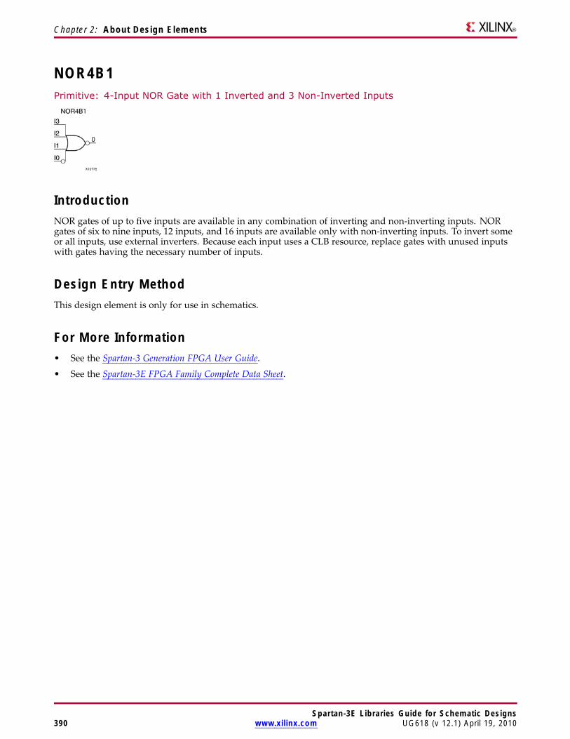
Chapter 2: About Design Elements
NOR4B1Primitive: 4-Input NOR Gate with 1 Inverted and 3 Non-Inverted Inputs
IntroductionNOR gates of up to five inputs are available in any combination of inverting and non-inverting inputs. NORgates of six to nine inputs, 12 inputs, and 16 inputs are available only with non-inverting inputs. To invert someor all inputs, use external inverters. Because each input uses a CLB resource, replace gates with unused inputswith gates having the necessary number of inputs.
Design Entry MethodThis design element is only for use in schematics.
For More Information• See the Spartan-3 Generation FPGA User Guide.
• See the Spartan-3E FPGA Family Complete Data Sheet.
Spartan-3E Libraries Guide for Schematic Designs390 www.xilinx.com UG618 (v 12.1) April 19, 2010
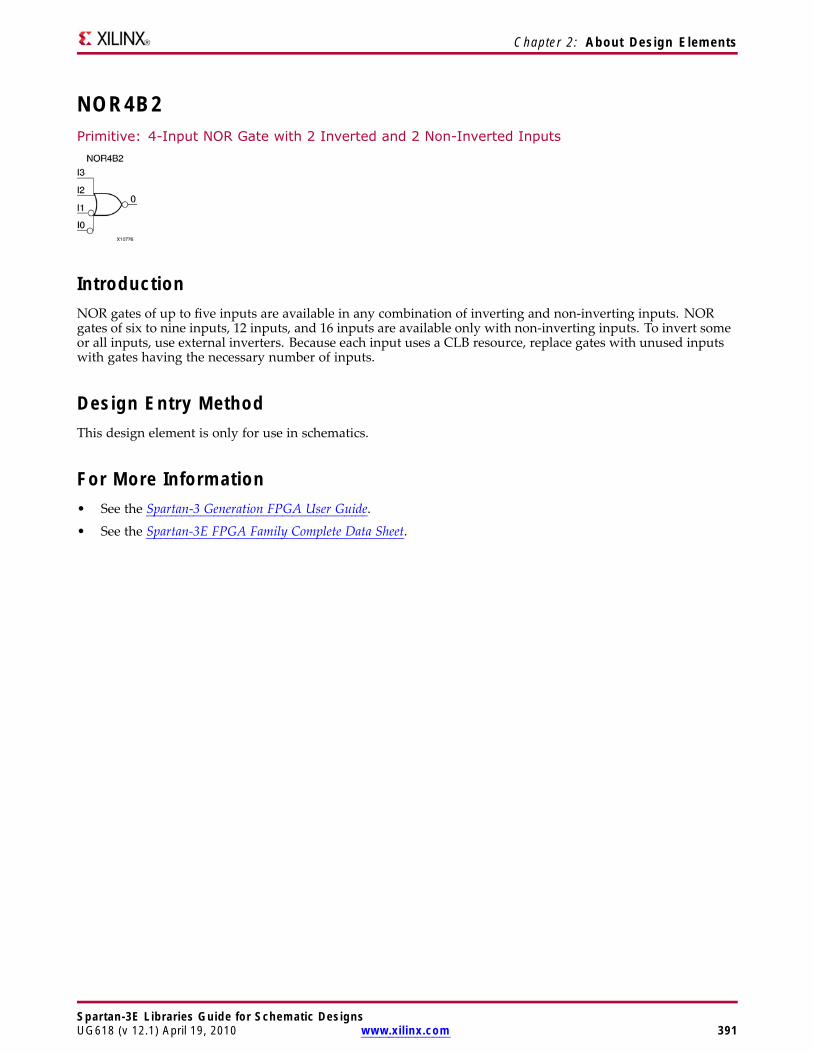
Chapter 2: About Design Elements
NOR4B2Primitive: 4-Input NOR Gate with 2 Inverted and 2 Non-Inverted Inputs
IntroductionNOR gates of up to five inputs are available in any combination of inverting and non-inverting inputs. NORgates of six to nine inputs, 12 inputs, and 16 inputs are available only with non-inverting inputs. To invert someor all inputs, use external inverters. Because each input uses a CLB resource, replace gates with unused inputswith gates having the necessary number of inputs.
Design Entry MethodThis design element is only for use in schematics.
For More Information• See the Spartan-3 Generation FPGA User Guide.
• See the Spartan-3E FPGA Family Complete Data Sheet.
Spartan-3E Libraries Guide for Schematic DesignsUG618 (v 12.1) April 19, 2010 www.xilinx.com 391

Chapter 2: About Design Elements
NOR4B3Primitive: 4-Input NOR Gate with 3 Inverted and 1 Non-Inverted Inputs
IntroductionNOR gates of up to five inputs are available in any combination of inverting and non-inverting inputs. NORgates of six to nine inputs, 12 inputs, and 16 inputs are available only with non-inverting inputs. To invert someor all inputs, use external inverters. Because each input uses a CLB resource, replace gates with unused inputswith gates having the necessary number of inputs.
Design Entry MethodThis design element is only for use in schematics.
For More Information• See the Spartan-3 Generation FPGA User Guide.
• See the Spartan-3E FPGA Family Complete Data Sheet.
Spartan-3E Libraries Guide for Schematic Designs392 www.xilinx.com UG618 (v 12.1) April 19, 2010
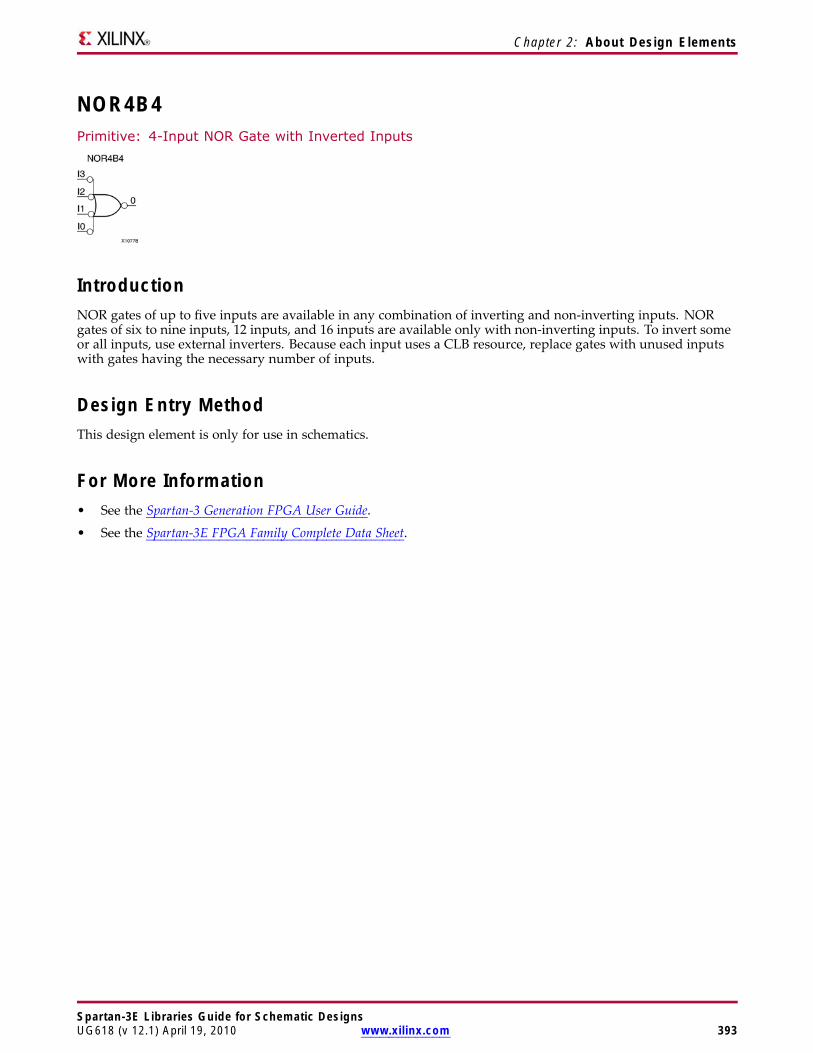
Chapter 2: About Design Elements
NOR4B4Primitive: 4-Input NOR Gate with Inverted Inputs
IntroductionNOR gates of up to five inputs are available in any combination of inverting and non-inverting inputs. NORgates of six to nine inputs, 12 inputs, and 16 inputs are available only with non-inverting inputs. To invert someor all inputs, use external inverters. Because each input uses a CLB resource, replace gates with unused inputswith gates having the necessary number of inputs.
Design Entry MethodThis design element is only for use in schematics.
For More Information• See the Spartan-3 Generation FPGA User Guide.
• See the Spartan-3E FPGA Family Complete Data Sheet.
Spartan-3E Libraries Guide for Schematic DesignsUG618 (v 12.1) April 19, 2010 www.xilinx.com 393
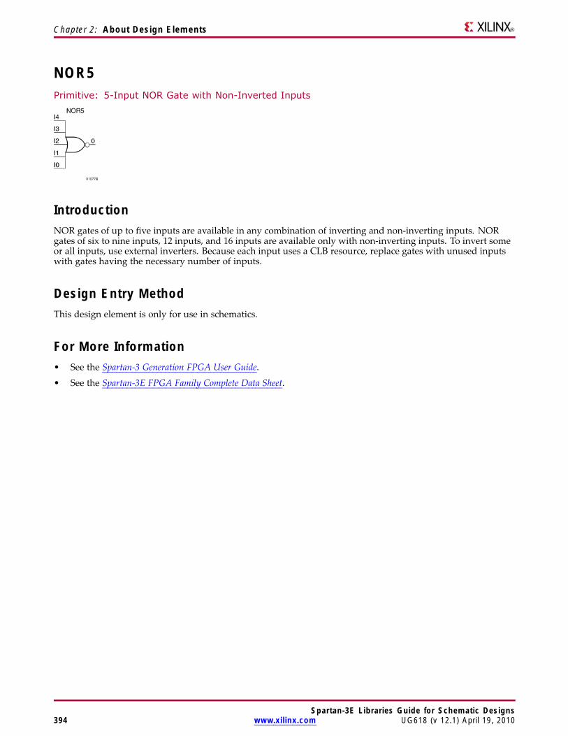
Chapter 2: About Design Elements
NOR5Primitive: 5-Input NOR Gate with Non-Inverted Inputs
IntroductionNOR gates of up to five inputs are available in any combination of inverting and non-inverting inputs. NORgates of six to nine inputs, 12 inputs, and 16 inputs are available only with non-inverting inputs. To invert someor all inputs, use external inverters. Because each input uses a CLB resource, replace gates with unused inputswith gates having the necessary number of inputs.
Design Entry MethodThis design element is only for use in schematics.
For More Information• See the Spartan-3 Generation FPGA User Guide.
• See the Spartan-3E FPGA Family Complete Data Sheet.
Spartan-3E Libraries Guide for Schematic Designs394 www.xilinx.com UG618 (v 12.1) April 19, 2010
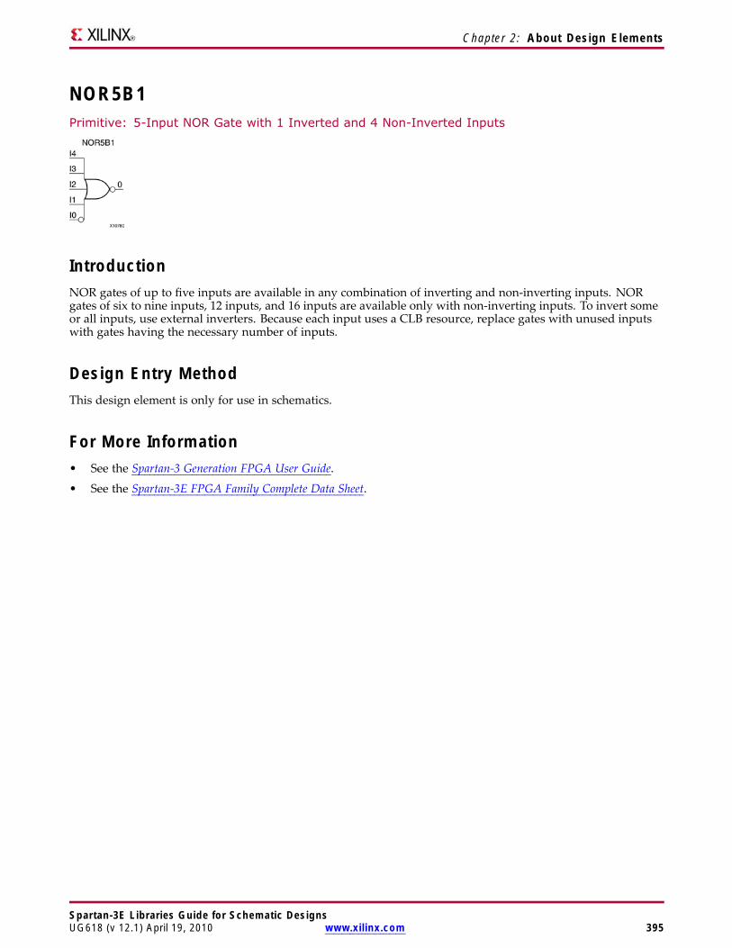
Chapter 2: About Design Elements
NOR5B1Primitive: 5-Input NOR Gate with 1 Inverted and 4 Non-Inverted Inputs
IntroductionNOR gates of up to five inputs are available in any combination of inverting and non-inverting inputs. NORgates of six to nine inputs, 12 inputs, and 16 inputs are available only with non-inverting inputs. To invert someor all inputs, use external inverters. Because each input uses a CLB resource, replace gates with unused inputswith gates having the necessary number of inputs.
Design Entry MethodThis design element is only for use in schematics.
For More Information• See the Spartan-3 Generation FPGA User Guide.
• See the Spartan-3E FPGA Family Complete Data Sheet.
Spartan-3E Libraries Guide for Schematic DesignsUG618 (v 12.1) April 19, 2010 www.xilinx.com 395

Chapter 2: About Design Elements
NOR5B2Primitive: 5-Input NOR Gate with 2 Inverted and 3 Non-Inverted Inputs
IntroductionNOR gates of up to five inputs are available in any combination of inverting and non-inverting inputs. NORgates of six to nine inputs, 12 inputs, and 16 inputs are available only with non-inverting inputs. To invert someor all inputs, use external inverters. Because each input uses a CLB resource, replace gates with unused inputswith gates having the necessary number of inputs.
Design Entry MethodThis design element is only for use in schematics.
For More Information• See the Spartan-3 Generation FPGA User Guide.
• See the Spartan-3E FPGA Family Complete Data Sheet.
Spartan-3E Libraries Guide for Schematic Designs396 www.xilinx.com UG618 (v 12.1) April 19, 2010
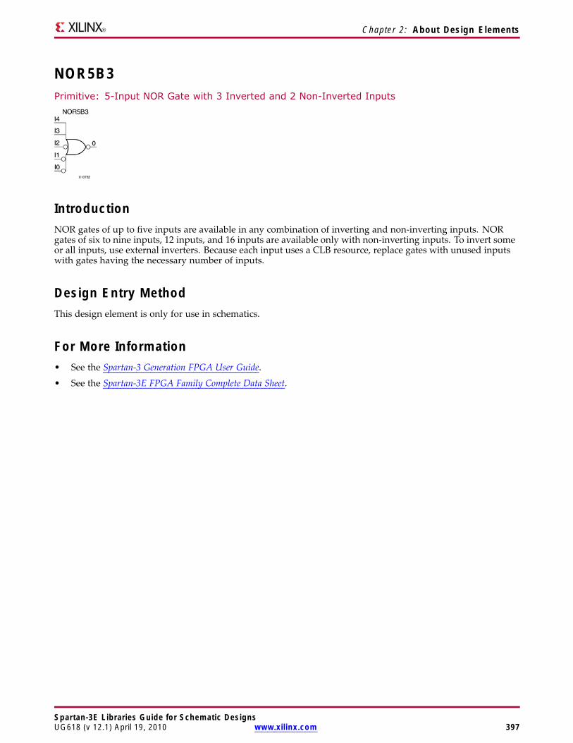
Chapter 2: About Design Elements
NOR5B3Primitive: 5-Input NOR Gate with 3 Inverted and 2 Non-Inverted Inputs
IntroductionNOR gates of up to five inputs are available in any combination of inverting and non-inverting inputs. NORgates of six to nine inputs, 12 inputs, and 16 inputs are available only with non-inverting inputs. To invert someor all inputs, use external inverters. Because each input uses a CLB resource, replace gates with unused inputswith gates having the necessary number of inputs.
Design Entry MethodThis design element is only for use in schematics.
For More Information• See the Spartan-3 Generation FPGA User Guide.
• See the Spartan-3E FPGA Family Complete Data Sheet.
Spartan-3E Libraries Guide for Schematic DesignsUG618 (v 12.1) April 19, 2010 www.xilinx.com 397
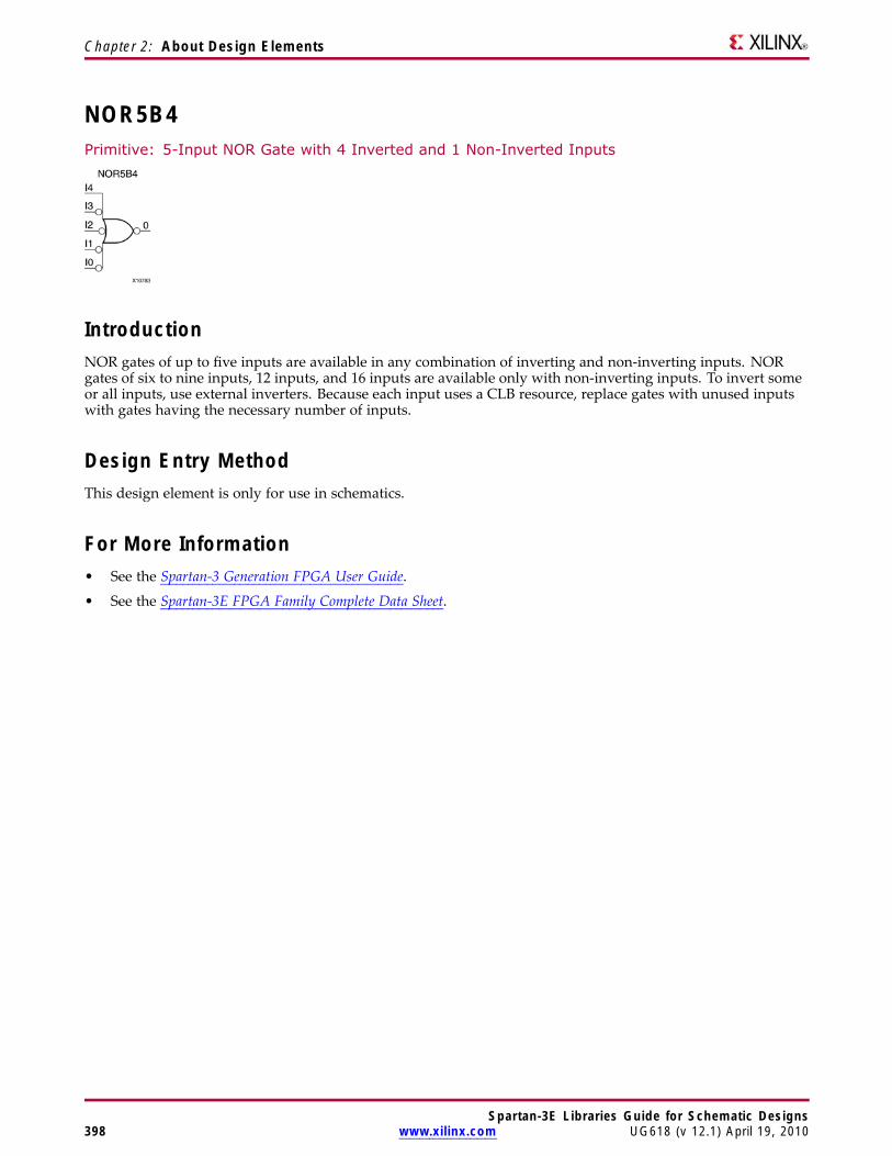
Chapter 2: About Design Elements
NOR5B4Primitive: 5-Input NOR Gate with 4 Inverted and 1 Non-Inverted Inputs
IntroductionNOR gates of up to five inputs are available in any combination of inverting and non-inverting inputs. NORgates of six to nine inputs, 12 inputs, and 16 inputs are available only with non-inverting inputs. To invert someor all inputs, use external inverters. Because each input uses a CLB resource, replace gates with unused inputswith gates having the necessary number of inputs.
Design Entry MethodThis design element is only for use in schematics.
For More Information• See the Spartan-3 Generation FPGA User Guide.
• See the Spartan-3E FPGA Family Complete Data Sheet.
Spartan-3E Libraries Guide for Schematic Designs398 www.xilinx.com UG618 (v 12.1) April 19, 2010

Chapter 2: About Design Elements
NOR5B5Primitive: 5-Input NOR Gate with Inverted Inputs
IntroductionNOR gates of up to five inputs are available in any combination of inverting and non-inverting inputs. NORgates of six to nine inputs, 12 inputs, and 16 inputs are available only with non-inverting inputs. To invert someor all inputs, use external inverters. Because each input uses a CLB resource, replace gates with unused inputswith gates having the necessary number of inputs.
Design Entry MethodThis design element is only for use in schematics.
For More Information• See the Spartan-3 Generation FPGA User Guide.
• See the Spartan-3E FPGA Family Complete Data Sheet.
Spartan-3E Libraries Guide for Schematic DesignsUG618 (v 12.1) April 19, 2010 www.xilinx.com 399

Chapter 2: About Design Elements
NOR6Macro: 6-Input NOR Gate with Non-Inverted Inputs
IntroductionNOR gates of up to five inputs are available in any combination of inverting and non-inverting inputs. NORgates of six to nine inputs, 12 inputs, and 16 inputs are available only with non-inverting inputs. To invert someor all inputs, use external inverters. Because each input uses a CLB resource, replace gates with unused inputswith gates having the necessary number of inputs.
Design Entry MethodThis design element is only for use in schematics.
For More Information• See the Spartan-3 Generation FPGA User Guide.
• See the Spartan-3E FPGA Family Complete Data Sheet.
Spartan-3E Libraries Guide for Schematic Designs400 www.xilinx.com UG618 (v 12.1) April 19, 2010
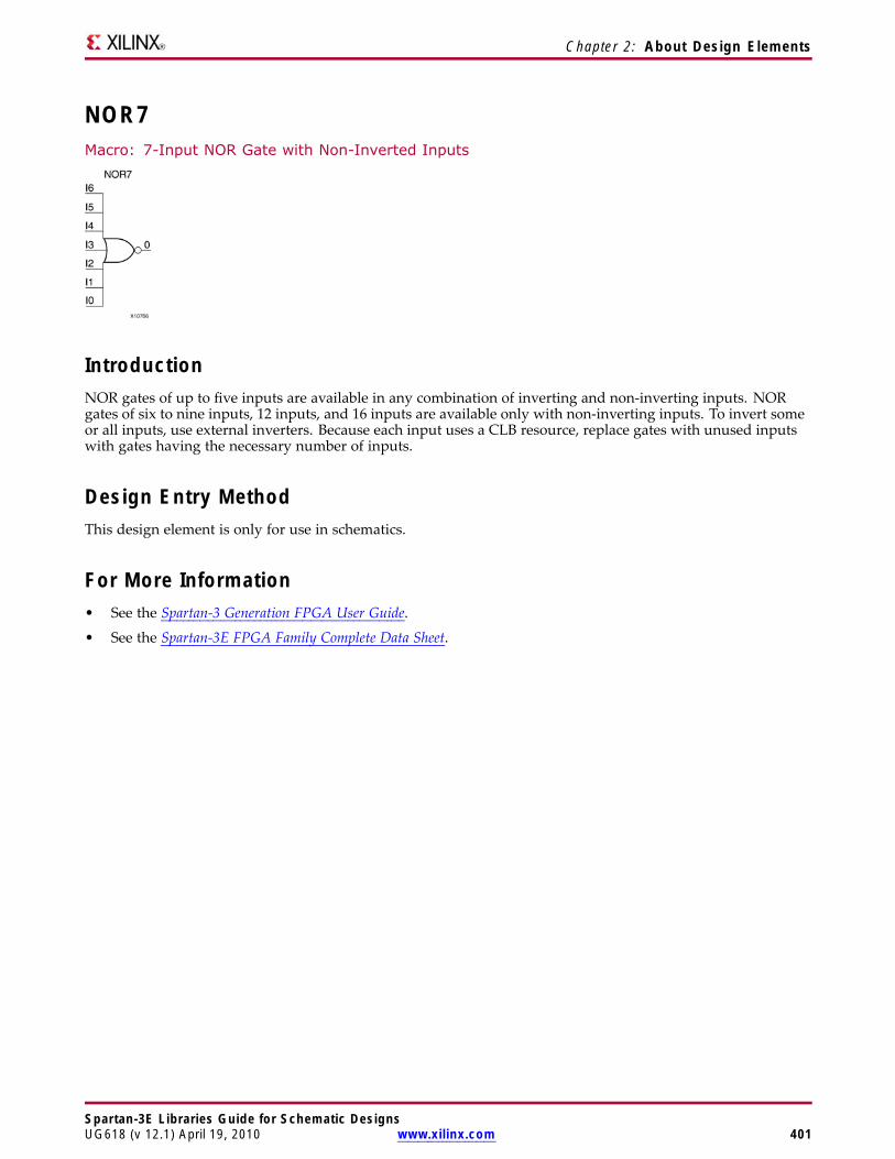
Chapter 2: About Design Elements
NOR7Macro: 7-Input NOR Gate with Non-Inverted Inputs
IntroductionNOR gates of up to five inputs are available in any combination of inverting and non-inverting inputs. NORgates of six to nine inputs, 12 inputs, and 16 inputs are available only with non-inverting inputs. To invert someor all inputs, use external inverters. Because each input uses a CLB resource, replace gates with unused inputswith gates having the necessary number of inputs.
Design Entry MethodThis design element is only for use in schematics.
For More Information• See the Spartan-3 Generation FPGA User Guide.
• See the Spartan-3E FPGA Family Complete Data Sheet.
Spartan-3E Libraries Guide for Schematic DesignsUG618 (v 12.1) April 19, 2010 www.xilinx.com 401
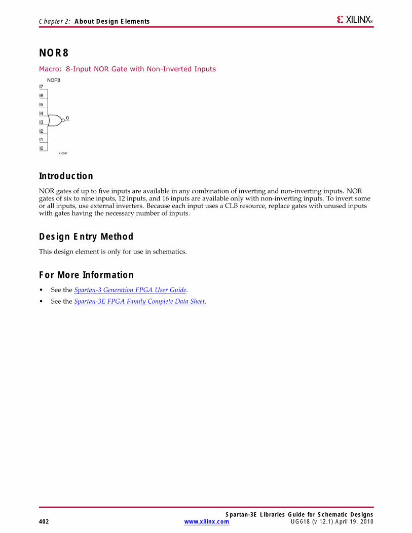
Chapter 2: About Design Elements
NOR8Macro: 8-Input NOR Gate with Non-Inverted Inputs
IntroductionNOR gates of up to five inputs are available in any combination of inverting and non-inverting inputs. NORgates of six to nine inputs, 12 inputs, and 16 inputs are available only with non-inverting inputs. To invert someor all inputs, use external inverters. Because each input uses a CLB resource, replace gates with unused inputswith gates having the necessary number of inputs.
Design Entry MethodThis design element is only for use in schematics.
For More Information• See the Spartan-3 Generation FPGA User Guide.
• See the Spartan-3E FPGA Family Complete Data Sheet.
Spartan-3E Libraries Guide for Schematic Designs402 www.xilinx.com UG618 (v 12.1) April 19, 2010
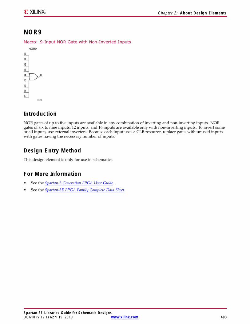
Chapter 2: About Design Elements
NOR9Macro: 9-Input NOR Gate with Non-Inverted Inputs
IntroductionNOR gates of up to five inputs are available in any combination of inverting and non-inverting inputs. NORgates of six to nine inputs, 12 inputs, and 16 inputs are available only with non-inverting inputs. To invert someor all inputs, use external inverters. Because each input uses a CLB resource, replace gates with unused inputswith gates having the necessary number of inputs.
Design Entry MethodThis design element is only for use in schematics.
For More Information• See the Spartan-3 Generation FPGA User Guide.
• See the Spartan-3E FPGA Family Complete Data Sheet.
Spartan-3E Libraries Guide for Schematic DesignsUG618 (v 12.1) April 19, 2010 www.xilinx.com 403
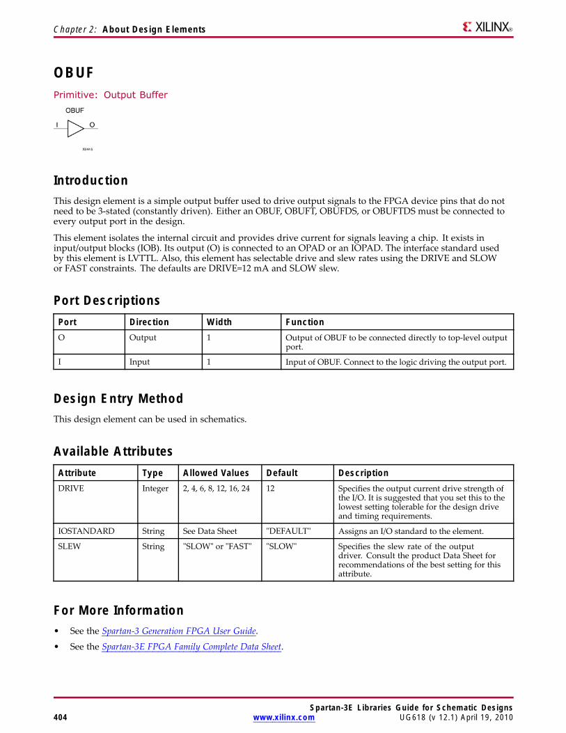
Chapter 2: About Design Elements
OBUFPrimitive: Output Buffer
IntroductionThis design element is a simple output buffer used to drive output signals to the FPGA device pins that do notneed to be 3-stated (constantly driven). Either an OBUF, OBUFT, OBUFDS, or OBUFTDS must be connected toevery output port in the design.
This element isolates the internal circuit and provides drive current for signals leaving a chip. It exists ininput/output blocks (IOB). Its output (O) is connected to an OPAD or an IOPAD. The interface standard usedby this element is LVTTL. Also, this element has selectable drive and slew rates using the DRIVE and SLOWor FAST constraints. The defaults are DRIVE=12 mA and SLOW slew.
Port DescriptionsPort Direction Width FunctionO Output 1 Output of OBUF to be connected directly to top-level output
port.
I Input 1 Input of OBUF. Connect to the logic driving the output port.
Design Entry MethodThis design element can be used in schematics.
Available AttributesAttribute Type Allowed Values Default DescriptionDRIVE Integer 2, 4, 6, 8, 12, 16, 24 12 Specifies the output current drive strength of
the I/O. It is suggested that you set this to thelowest setting tolerable for the design driveand timing requirements.
IOSTANDARD String See Data Sheet "DEFAULT" Assigns an I/O standard to the element.
SLEW String "SLOW" or "FAST" "SLOW" Specifies the slew rate of the outputdriver. Consult the product Data Sheet forrecommendations of the best setting for thisattribute.
For More Information• See the Spartan-3 Generation FPGA User Guide.
• See the Spartan-3E FPGA Family Complete Data Sheet.
Spartan-3E Libraries Guide for Schematic Designs404 www.xilinx.com UG618 (v 12.1) April 19, 2010
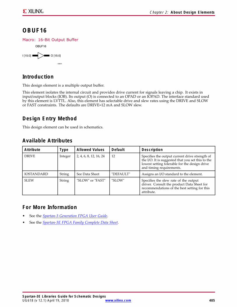
Chapter 2: About Design Elements
OBUF16Macro: 16-Bit Output Buffer
IntroductionThis design element is a multiple output buffer.
This element isolates the internal circuit and provides drive current for signals leaving a chip. It exists ininput/output blocks (IOB). Its output (O) is connected to an OPAD or an IOPAD. The interface standard usedby this element is LVTTL. Also, this element has selectable drive and slew rates using the DRIVE and SLOWor FAST constraints. The defaults are DRIVE=12 mA and SLOW slew.
Design Entry MethodThis design element can be used in schematics.
Available AttributesAttribute Type Allowed Values Default DescriptionDRIVE Integer 2, 4, 6, 8, 12, 16, 24 12 Specifies the output current drive strength of
the I/O. It is suggested that you set this to thelowest setting tolerable for the design driveand timing requirements.
IOSTANDARD String See Data Sheet "DEFAULT" Assigns an I/O standard to the element.
SLEW String "SLOW" or "FAST" "SLOW" Specifies the slew rate of the outputdriver. Consult the product Data Sheet forrecommendations of the best setting for thisattribute.
For More Information• See the Spartan-3 Generation FPGA User Guide.
• See the Spartan-3E FPGA Family Complete Data Sheet.
Spartan-3E Libraries Guide for Schematic DesignsUG618 (v 12.1) April 19, 2010 www.xilinx.com 405
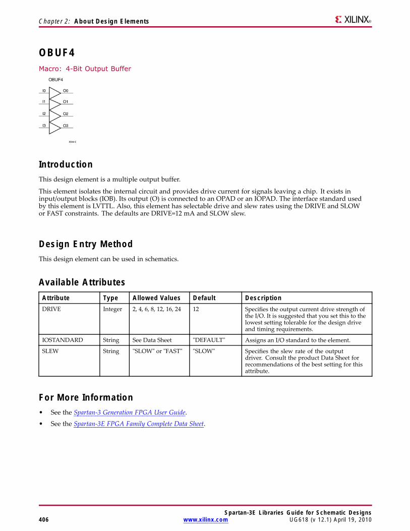
Chapter 2: About Design Elements
OBUF4Macro: 4-Bit Output Buffer
IntroductionThis design element is a multiple output buffer.
This element isolates the internal circuit and provides drive current for signals leaving a chip. It exists ininput/output blocks (IOB). Its output (O) is connected to an OPAD or an IOPAD. The interface standard usedby this element is LVTTL. Also, this element has selectable drive and slew rates using the DRIVE and SLOWor FAST constraints. The defaults are DRIVE=12 mA and SLOW slew.
Design Entry MethodThis design element can be used in schematics.
Available AttributesAttribute Type Allowed Values Default DescriptionDRIVE Integer 2, 4, 6, 8, 12, 16, 24 12 Specifies the output current drive strength of
the I/O. It is suggested that you set this to thelowest setting tolerable for the design driveand timing requirements.
IOSTANDARD String See Data Sheet "DEFAULT" Assigns an I/O standard to the element.
SLEW String "SLOW" or "FAST" "SLOW" Specifies the slew rate of the outputdriver. Consult the product Data Sheet forrecommendations of the best setting for thisattribute.
For More Information• See the Spartan-3 Generation FPGA User Guide.
• See the Spartan-3E FPGA Family Complete Data Sheet.
Spartan-3E Libraries Guide for Schematic Designs406 www.xilinx.com UG618 (v 12.1) April 19, 2010

Chapter 2: About Design Elements
OBUF8Macro: 8-Bit Output Buffer
IntroductionThis design element is a multiple output buffer.
This element isolates the internal circuit and provides drive current for signals leaving a chip. It exists ininput/output blocks (IOB). Its output (O) is connected to an OPAD or an IOPAD. The interface standard usedby this element is LVTTL. Also, this element has selectable drive and slew rates using the DRIVE and SLOWor FAST constraints. The defaults are DRIVE=12 mA and SLOW slew.
Design Entry MethodThis design element can be used in schematics.
Available AttributesAttribute Type Allowed Values Default DescriptionDRIVE Integer 2, 4, 6, 8, 12, 16, 24 12 Specifies the output current drive strength of
the I/O. It is suggested that you set this to thelowest setting tolerable for the design driveand timing requirements.
IOSTANDARD String See Data Sheet "DEFAULT" Assigns an I/O standard to the element.
SLEW String "SLOW" or "FAST" "SLOW" Specifies the slew rate of the outputdriver. Consult the product Data Sheet forrecommendations of the best setting for thisattribute.
For More Information• See the Spartan-3 Generation FPGA User Guide.
• See the Spartan-3E FPGA Family Complete Data Sheet.
Spartan-3E Libraries Guide for Schematic DesignsUG618 (v 12.1) April 19, 2010 www.xilinx.com 407
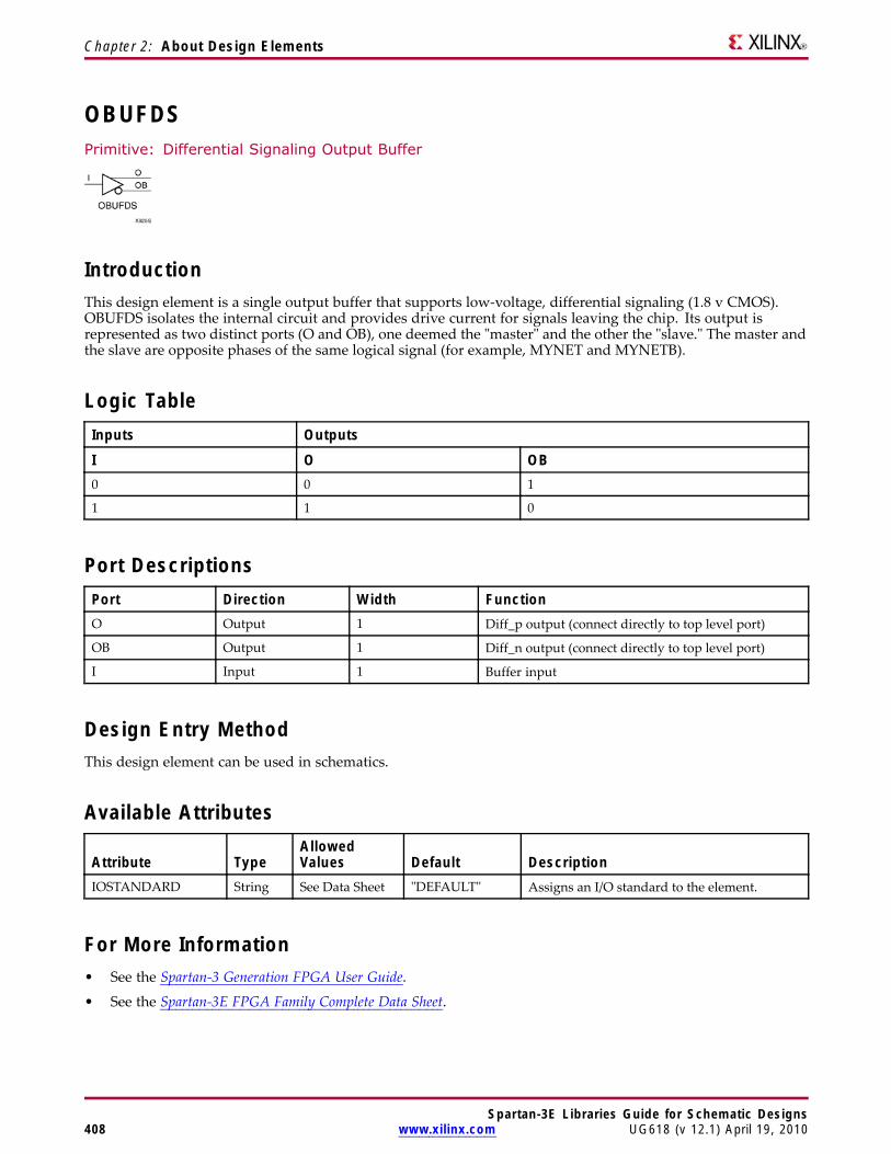
Chapter 2: About Design Elements
OBUFDSPrimitive: Differential Signaling Output Buffer
IntroductionThis design element is a single output buffer that supports low-voltage, differential signaling (1.8 v CMOS).OBUFDS isolates the internal circuit and provides drive current for signals leaving the chip. Its output isrepresented as two distinct ports (O and OB), one deemed the "master" and the other the "slave." The master andthe slave are opposite phases of the same logical signal (for example, MYNET and MYNETB).
Logic TableInputs Outputs
I O OB0 0 1
1 1 0
Port DescriptionsPort Direction Width FunctionO Output 1 Diff_p output (connect directly to top level port)
OB Output 1 Diff_n output (connect directly to top level port)
I Input 1 Buffer input
Design Entry MethodThis design element can be used in schematics.
Available Attributes
Attribute TypeAllowedValues Default Description
IOSTANDARD String See Data Sheet "DEFAULT" Assigns an I/O standard to the element.
For More Information• See the Spartan-3 Generation FPGA User Guide.
• See the Spartan-3E FPGA Family Complete Data Sheet.
Spartan-3E Libraries Guide for Schematic Designs408 www.xilinx.com UG618 (v 12.1) April 19, 2010
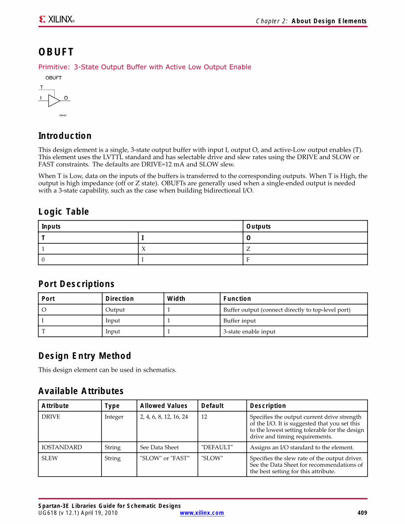
Chapter 2: About Design Elements
OBUFTPrimitive: 3-State Output Buffer with Active Low Output Enable
IntroductionThis design element is a single, 3-state output buffer with input I, output O, and active-Low output enables (T).This element uses the LVTTL standard and has selectable drive and slew rates using the DRIVE and SLOW orFAST constraints. The defaults are DRIVE=12 mA and SLOW slew.
When T is Low, data on the inputs of the buffers is transferred to the corresponding outputs. When T is High, theoutput is high impedance (off or Z state). OBUFTs are generally used when a single-ended output is neededwith a 3-state capability, such as the case when building bidirectional I/O.
Logic TableInputs Outputs
T I O1 X Z
0 I F
Port DescriptionsPort Direction Width FunctionO Output 1 Buffer output (connect directly to top-level port)
I Input 1 Buffer input
T Input 1 3-state enable input
Design Entry MethodThis design element can be used in schematics.
Available AttributesAttribute Type Allowed Values Default DescriptionDRIVE Integer 2, 4, 6, 8, 12, 16, 24 12 Specifies the output current drive strength
of the I/O. It is suggested that you set thisto the lowest setting tolerable for the designdrive and timing requirements.
IOSTANDARD String See Data Sheet "DEFAULT" Assigns an I/O standard to the element.
SLEW String "SLOW" or "FAST” "SLOW" Specifies the slew rate of the output driver.See the Data Sheet for recommendations ofthe best setting for this attribute.
Spartan-3E Libraries Guide for Schematic DesignsUG618 (v 12.1) April 19, 2010 www.xilinx.com 409

Chapter 2: About Design Elements
For More Information• See the Spartan-3 Generation FPGA User Guide.
• See the Spartan-3E FPGA Family Complete Data Sheet.
Spartan-3E Libraries Guide for Schematic Designs410 www.xilinx.com UG618 (v 12.1) April 19, 2010
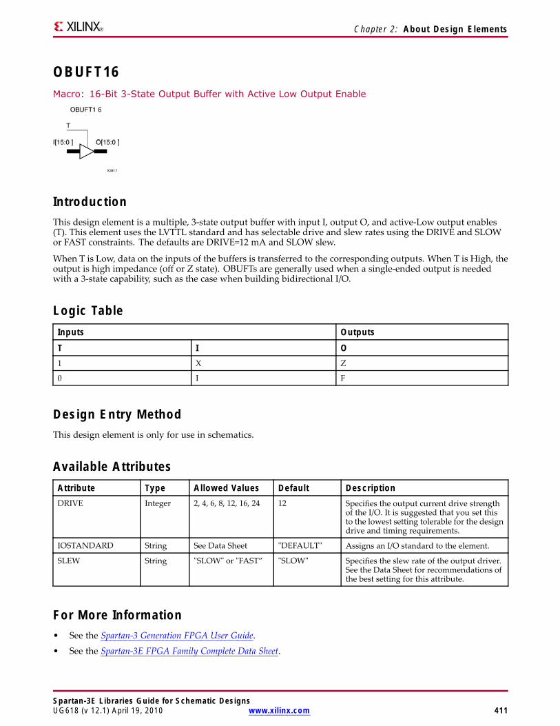
Chapter 2: About Design Elements
OBUFT16Macro: 16-Bit 3-State Output Buffer with Active Low Output Enable
IntroductionThis design element is a multiple, 3-state output buffer with input I, output O, and active-Low output enables(T). This element uses the LVTTL standard and has selectable drive and slew rates using the DRIVE and SLOWor FAST constraints. The defaults are DRIVE=12 mA and SLOW slew.
When T is Low, data on the inputs of the buffers is transferred to the corresponding outputs. When T is High, theoutput is high impedance (off or Z state). OBUFTs are generally used when a single-ended output is neededwith a 3-state capability, such as the case when building bidirectional I/O.
Logic TableInputs Outputs
T I O1 X Z
0 I F
Design Entry MethodThis design element is only for use in schematics.
Available AttributesAttribute Type Allowed Values Default DescriptionDRIVE Integer 2, 4, 6, 8, 12, 16, 24 12 Specifies the output current drive strength
of the I/O. It is suggested that you set thisto the lowest setting tolerable for the designdrive and timing requirements.
IOSTANDARD String See Data Sheet "DEFAULT" Assigns an I/O standard to the element.
SLEW String "SLOW" or "FAST” "SLOW" Specifies the slew rate of the output driver.See the Data Sheet for recommendations ofthe best setting for this attribute.
For More Information• See the Spartan-3 Generation FPGA User Guide.
• See the Spartan-3E FPGA Family Complete Data Sheet.
Spartan-3E Libraries Guide for Schematic DesignsUG618 (v 12.1) April 19, 2010 www.xilinx.com 411
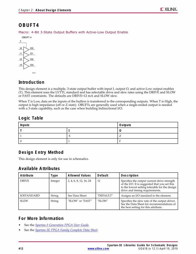
Chapter 2: About Design Elements
OBUFT4Macro: 4-Bit 3-State Output Buffers with Active-Low Output Enable
IntroductionThis design element is a multiple, 3-state output buffer with input I, output O, and active-Low output enables(T). This element uses the LVTTL standard and has selectable drive and slew rates using the DRIVE and SLOWor FAST constraints. The defaults are DRIVE=12 mA and SLOW slew.
When T is Low, data on the inputs of the buffers is transferred to the corresponding outputs. When T is High, theoutput is high impedance (off or Z state). OBUFTs are generally used when a single-ended output is neededwith a 3-state capability, such as the case when building bidirectional I/O.
Logic TableInputs Outputs
T I O1 X Z
0 I F
Design Entry MethodThis design element is only for use in schematics.
Available AttributesAttribute Type Allowed Values Default DescriptionDRIVE Integer 2, 4, 6, 8, 12, 16, 24 12 Specifies the output current drive strength
of the I/O. It is suggested that you set thisto the lowest setting tolerable for the designdrive and timing requirements.
IOSTANDARD String See Data Sheet "DEFAULT" Assigns an I/O standard to the element.
SLEW String "SLOW" or "FAST” "SLOW" Specifies the slew rate of the output driver.See the Data Sheet for recommendations ofthe best setting for this attribute.
For More Information• See the Spartan-3 Generation FPGA User Guide.• See the Spartan-3E FPGA Family Complete Data Sheet.
Spartan-3E Libraries Guide for Schematic Designs412 www.xilinx.com UG618 (v 12.1) April 19, 2010
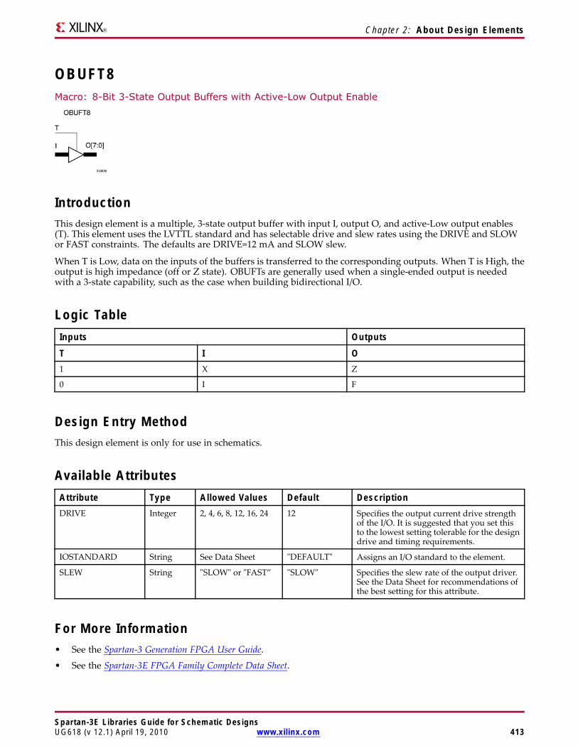
Chapter 2: About Design Elements
OBUFT8Macro: 8-Bit 3-State Output Buffers with Active-Low Output Enable
IntroductionThis design element is a multiple, 3-state output buffer with input I, output O, and active-Low output enables(T). This element uses the LVTTL standard and has selectable drive and slew rates using the DRIVE and SLOWor FAST constraints. The defaults are DRIVE=12 mA and SLOW slew.
When T is Low, data on the inputs of the buffers is transferred to the corresponding outputs. When T is High, theoutput is high impedance (off or Z state). OBUFTs are generally used when a single-ended output is neededwith a 3-state capability, such as the case when building bidirectional I/O.
Logic TableInputs Outputs
T I O1 X Z
0 I F
Design Entry MethodThis design element is only for use in schematics.
Available AttributesAttribute Type Allowed Values Default DescriptionDRIVE Integer 2, 4, 6, 8, 12, 16, 24 12 Specifies the output current drive strength
of the I/O. It is suggested that you set thisto the lowest setting tolerable for the designdrive and timing requirements.
IOSTANDARD String See Data Sheet "DEFAULT" Assigns an I/O standard to the element.
SLEW String "SLOW" or "FAST” "SLOW" Specifies the slew rate of the output driver.See the Data Sheet for recommendations ofthe best setting for this attribute.
For More Information• See the Spartan-3 Generation FPGA User Guide.
• See the Spartan-3E FPGA Family Complete Data Sheet.
Spartan-3E Libraries Guide for Schematic DesignsUG618 (v 12.1) April 19, 2010 www.xilinx.com 413
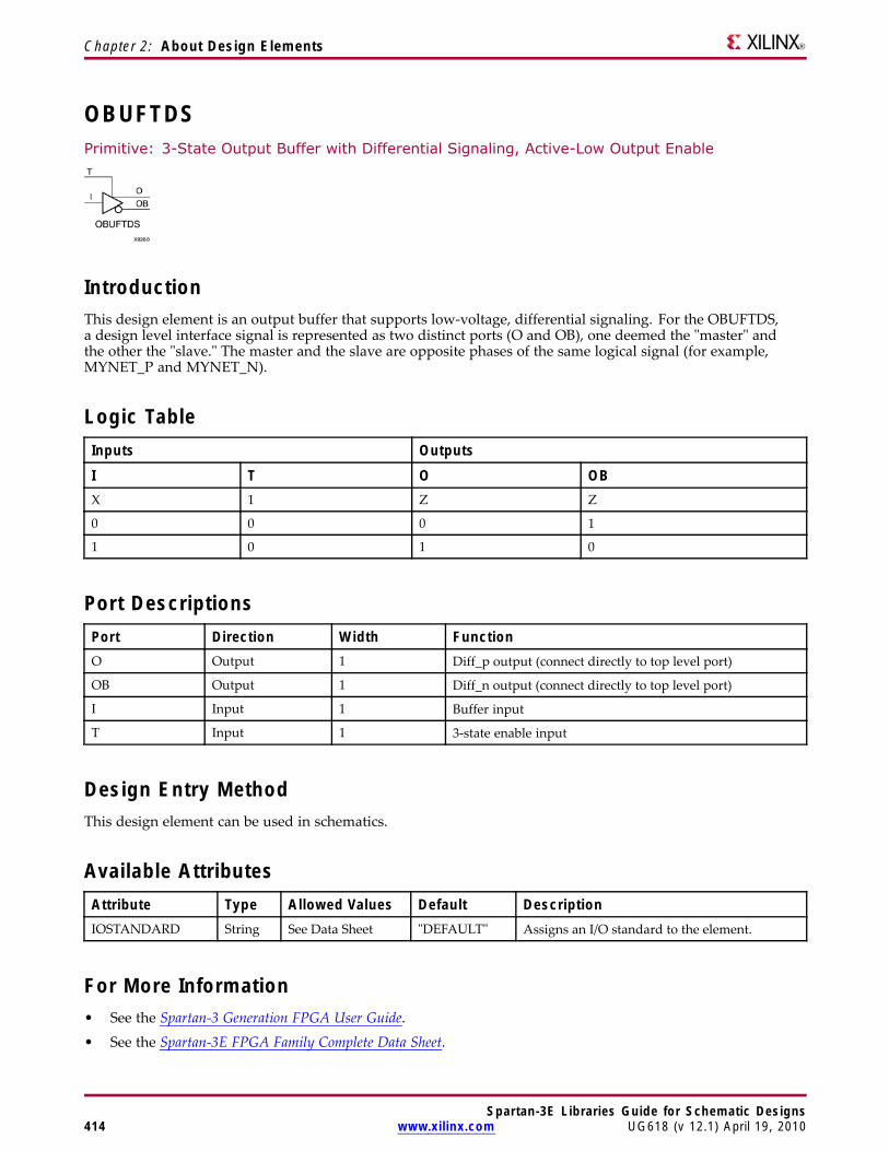
Chapter 2: About Design Elements
OBUFTDSPrimitive: 3-State Output Buffer with Differential Signaling, Active-Low Output Enable
IntroductionThis design element is an output buffer that supports low-voltage, differential signaling. For the OBUFTDS,a design level interface signal is represented as two distinct ports (O and OB), one deemed the "master" andthe other the "slave." The master and the slave are opposite phases of the same logical signal (for example,MYNET_P and MYNET_N).
Logic TableInputs Outputs
I T O OBX 1 Z Z
0 0 0 1
1 0 1 0
Port DescriptionsPort Direction Width FunctionO Output 1 Diff_p output (connect directly to top level port)
OB Output 1 Diff_n output (connect directly to top level port)
I Input 1 Buffer input
T Input 1 3-state enable input
Design Entry MethodThis design element can be used in schematics.
Available AttributesAttribute Type Allowed Values Default DescriptionIOSTANDARD String See Data Sheet "DEFAULT" Assigns an I/O standard to the element.
For More Information• See the Spartan-3 Generation FPGA User Guide.
• See the Spartan-3E FPGA Family Complete Data Sheet.
Spartan-3E Libraries Guide for Schematic Designs414 www.xilinx.com UG618 (v 12.1) April 19, 2010
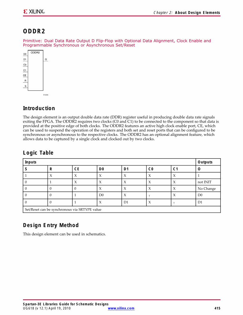
Chapter 2: About Design Elements
ODDR2Primitive: Dual Data Rate Output D Flip-Flop with Optional Data Alignment, Clock Enable andProgrammable Synchronous or Asynchronous Set/Reset
IntroductionThe design element is an output double data rate (DDR) register useful in producing double data rate signalsexiting the FPGA. The ODDR2 requires two clocks (C0 and C1) to be connected to the component so that data isprovided at the positive edge of both clocks. The ODDR2 features an active high clock enable port, CE, whichcan be used to suspend the operation of the registers and both set and reset ports that can be configured to besynchronous or asynchronous to the respective clocks. The ODDR2 has an optional alignment feature, whichallows data to be captured by a single clock and clocked out by two clocks.
Logic TableInputs Outputs
S R CE D0 D1 C0 C1 O1 X X X X X X 1
0 1 X X X X X not INIT
0 0 0 X X X X No Change
0 0 1 D0 X ↑ X D0
0 0 1 X D1 X ↑ D1
Set/Reset can be synchronous via SRTYPE value
Design Entry MethodThis design element can be used in schematics.
Spartan-3E Libraries Guide for Schematic DesignsUG618 (v 12.1) April 19, 2010 www.xilinx.com 415
Chapter 2: About Design Elements
Available AttributesAttribute Type Allowed Values Default DescriptionsDDR_ALIGNMENT String "NONE", "C0",
"C1”"NONE” Sets the input capture behavior for the DDR
register. "NONE" clocks in data to the D0input on the positive transition of the C0 clockand D1 on the positive transition of the C1clock. "C0" allows the input clocking of bothD0 and D1 align to the positive edge of theC0 clock. "C1" allows the input clocking ofboth D0 and D1 align to the positive edge ofthe C1 clock.
INIT Integer 0, 1 0 Sets initial state of the Q0 output to 0 or 1.
SRTYPE String "SYNC","ASYNC”
"SYNC” Specifies "SYNC" or "ASYNC" set/reset.
For More Information• See the Spartan-3 Generation FPGA User Guide.
• See the Spartan-3E FPGA Family Complete Data Sheet.
Spartan-3E Libraries Guide for Schematic Designs416 www.xilinx.com UG618 (v 12.1) April 19, 2010
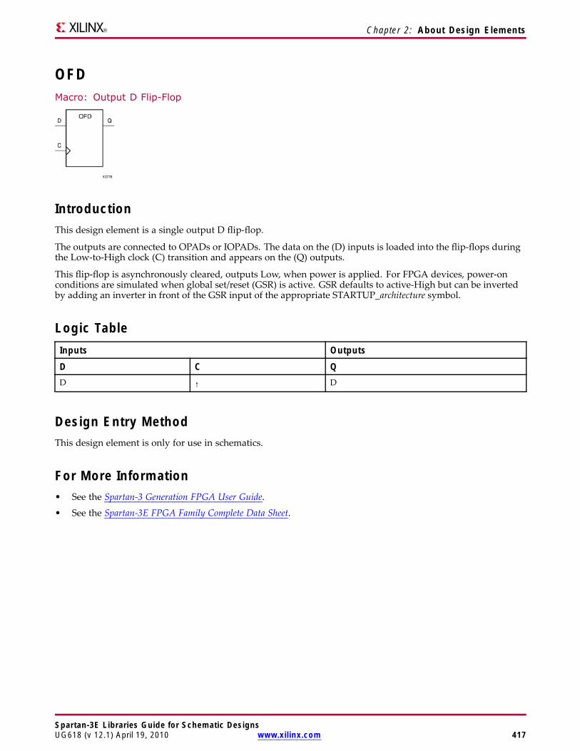
Chapter 2: About Design Elements
OFDMacro: Output D Flip-Flop
IntroductionThis design element is a single output D flip-flop.
The outputs are connected to OPADs or IOPADs. The data on the (D) inputs is loaded into the flip-flops duringthe Low-to-High clock (C) transition and appears on the (Q) outputs.
This flip-flop is asynchronously cleared, outputs Low, when power is applied. For FPGA devices, power-onconditions are simulated when global set/reset (GSR) is active. GSR defaults to active-High but can be invertedby adding an inverter in front of the GSR input of the appropriate STARTUP_architecture symbol.
Logic TableInputs Outputs
D C QD ↑ D
Design Entry MethodThis design element is only for use in schematics.
For More Information• See the Spartan-3 Generation FPGA User Guide.
• See the Spartan-3E FPGA Family Complete Data Sheet.
Spartan-3E Libraries Guide for Schematic DesignsUG618 (v 12.1) April 19, 2010 www.xilinx.com 417
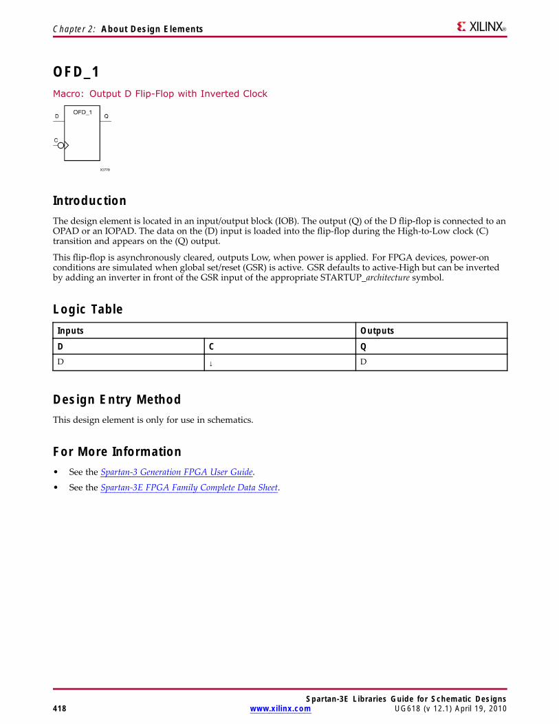
Chapter 2: About Design Elements
OFD_1Macro: Output D Flip-Flop with Inverted Clock
IntroductionThe design element is located in an input/output block (IOB). The output (Q) of the D flip-flop is connected to anOPAD or an IOPAD. The data on the (D) input is loaded into the flip-flop during the High-to-Low clock (C)transition and appears on the (Q) output.
This flip-flop is asynchronously cleared, outputs Low, when power is applied. For FPGA devices, power-onconditions are simulated when global set/reset (GSR) is active. GSR defaults to active-High but can be invertedby adding an inverter in front of the GSR input of the appropriate STARTUP_architecture symbol.
Logic TableInputs Outputs
D C QD ↓ D
Design Entry MethodThis design element is only for use in schematics.
For More Information• See the Spartan-3 Generation FPGA User Guide.
• See the Spartan-3E FPGA Family Complete Data Sheet.
Spartan-3E Libraries Guide for Schematic Designs418 www.xilinx.com UG618 (v 12.1) April 19, 2010
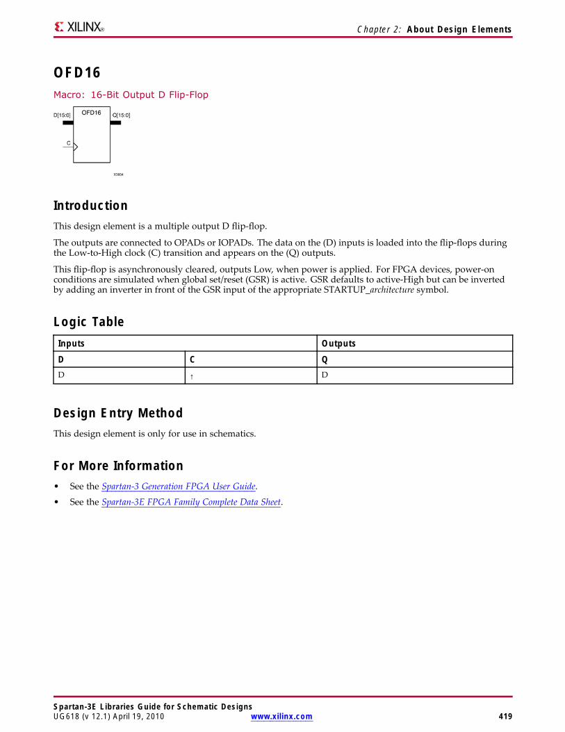
Chapter 2: About Design Elements
OFD16Macro: 16-Bit Output D Flip-Flop
IntroductionThis design element is a multiple output D flip-flop.
The outputs are connected to OPADs or IOPADs. The data on the (D) inputs is loaded into the flip-flops duringthe Low-to-High clock (C) transition and appears on the (Q) outputs.
This flip-flop is asynchronously cleared, outputs Low, when power is applied. For FPGA devices, power-onconditions are simulated when global set/reset (GSR) is active. GSR defaults to active-High but can be invertedby adding an inverter in front of the GSR input of the appropriate STARTUP_architecture symbol.
Logic TableInputs Outputs
D C QD ↑ D
Design Entry MethodThis design element is only for use in schematics.
For More Information• See the Spartan-3 Generation FPGA User Guide.
• See the Spartan-3E FPGA Family Complete Data Sheet.
Spartan-3E Libraries Guide for Schematic DesignsUG618 (v 12.1) April 19, 2010 www.xilinx.com 419
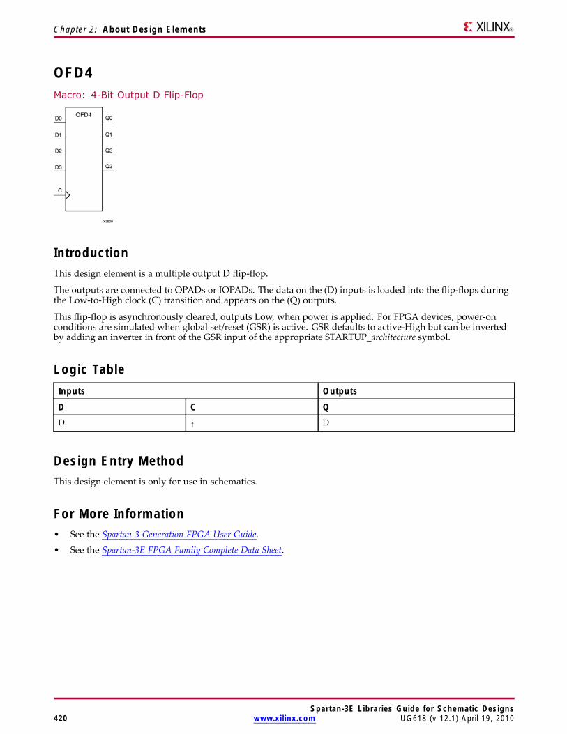
Chapter 2: About Design Elements
OFD4Macro: 4-Bit Output D Flip-Flop
IntroductionThis design element is a multiple output D flip-flop.
The outputs are connected to OPADs or IOPADs. The data on the (D) inputs is loaded into the flip-flops duringthe Low-to-High clock (C) transition and appears on the (Q) outputs.
This flip-flop is asynchronously cleared, outputs Low, when power is applied. For FPGA devices, power-onconditions are simulated when global set/reset (GSR) is active. GSR defaults to active-High but can be invertedby adding an inverter in front of the GSR input of the appropriate STARTUP_architecture symbol.
Logic TableInputs Outputs
D C QD ↑ D
Design Entry MethodThis design element is only for use in schematics.
For More Information• See the Spartan-3 Generation FPGA User Guide.
• See the Spartan-3E FPGA Family Complete Data Sheet.
Spartan-3E Libraries Guide for Schematic Designs420 www.xilinx.com UG618 (v 12.1) April 19, 2010
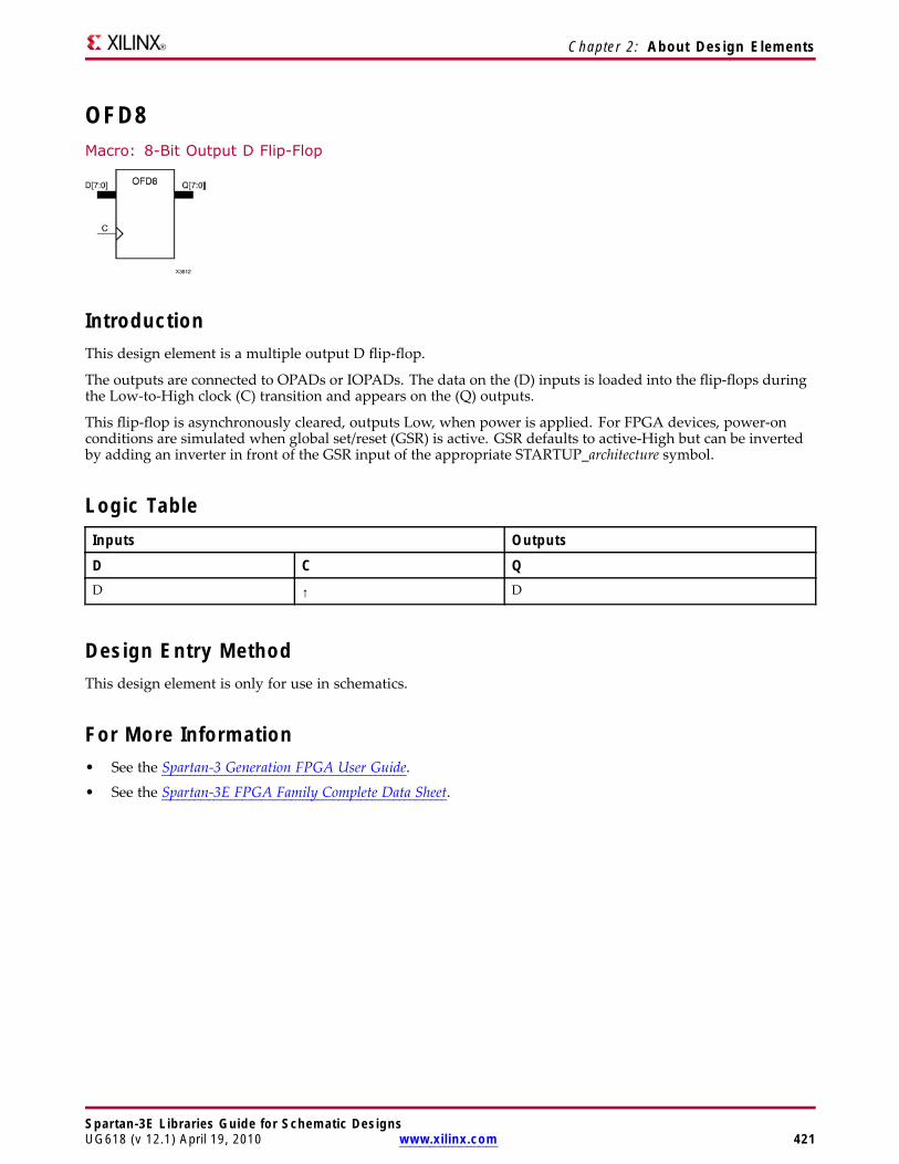
Chapter 2: About Design Elements
OFD8Macro: 8-Bit Output D Flip-Flop
IntroductionThis design element is a multiple output D flip-flop.
The outputs are connected to OPADs or IOPADs. The data on the (D) inputs is loaded into the flip-flops duringthe Low-to-High clock (C) transition and appears on the (Q) outputs.
This flip-flop is asynchronously cleared, outputs Low, when power is applied. For FPGA devices, power-onconditions are simulated when global set/reset (GSR) is active. GSR defaults to active-High but can be invertedby adding an inverter in front of the GSR input of the appropriate STARTUP_architecture symbol.
Logic TableInputs Outputs
D C QD ↑ D
Design Entry MethodThis design element is only for use in schematics.
For More Information• See the Spartan-3 Generation FPGA User Guide.
• See the Spartan-3E FPGA Family Complete Data Sheet.
Spartan-3E Libraries Guide for Schematic DesignsUG618 (v 12.1) April 19, 2010 www.xilinx.com 421
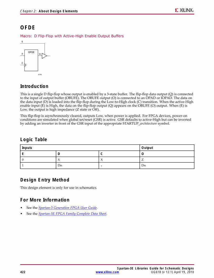
Chapter 2: About Design Elements
OFDEMacro: D Flip-Flop with Active-High Enable Output Buffers
IntroductionThis is a single D flip-flop whose output is enabled by a 3-state buffer. The flip-flop data output (Q) is connectedto the input of output buffer (OBUFE). The OBUFE output (O) is connected to an OPAD or IOPAD. The data onthe data input (D) is loaded into the flip-flop during the Low-to-High clock (C) transition. When the active-Highenable input (E) is High, the data on the flip-flop output (Q) appears on the OBUFE (O) output. When (E) isLow, the output is high impedance (Z state or Off).
This flip-flop is asynchronously cleared, outputs Low, when power is applied. For FPGA devices, power-onconditions are simulated when global set/reset (GSR) is active. GSR defaults to active-High but can be invertedby adding an inverter in front of the GSR input of the appropriate STARTUP_architecture symbol.
Logic TableInputs Output
E D C O0 X X Z
1 Dn ↑ Dn
Design Entry MethodThis design element is only for use in schematics.
For More Information• See the Spartan-3 Generation FPGA User Guide.
• See the Spartan-3E FPGA Family Complete Data Sheet.
Spartan-3E Libraries Guide for Schematic Designs422 www.xilinx.com UG618 (v 12.1) April 19, 2010
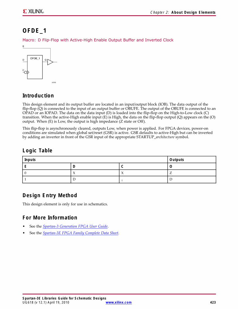
Chapter 2: About Design Elements
OFDE_1Macro: D Flip-Flop with Active-High Enable Output Buffer and Inverted Clock
IntroductionThis design element and its output buffer are located in an input/output block (IOB). The data output of theflip-flop (Q) is connected to the input of an output buffer or OBUFE. The output of the OBUFE is connected to anOPAD or an IOPAD. The data on the data input (D) is loaded into the flip-flop on the High-to-Low clock (C)transition. When the active-High enable input (E) is High, the data on the flip-flop output (Q) appears on the (O)output. When (E) is Low, the output is high impedance (Z state or Off).
This flip-flop is asynchronously cleared, outputs Low, when power is applied. For FPGA devices, power-onconditions are simulated when global set/reset (GSR) is active. GSR defaults to active-High but can be invertedby adding an inverter in front of the GSR input of the appropriate STARTUP_architecture symbol.
Logic TableInputs Outputs
E D C O0 X X Z
1 D ↓ D
Design Entry MethodThis design element is only for use in schematics.
For More Information• See the Spartan-3 Generation FPGA User Guide.
• See the Spartan-3E FPGA Family Complete Data Sheet.
Spartan-3E Libraries Guide for Schematic DesignsUG618 (v 12.1) April 19, 2010 www.xilinx.com 423
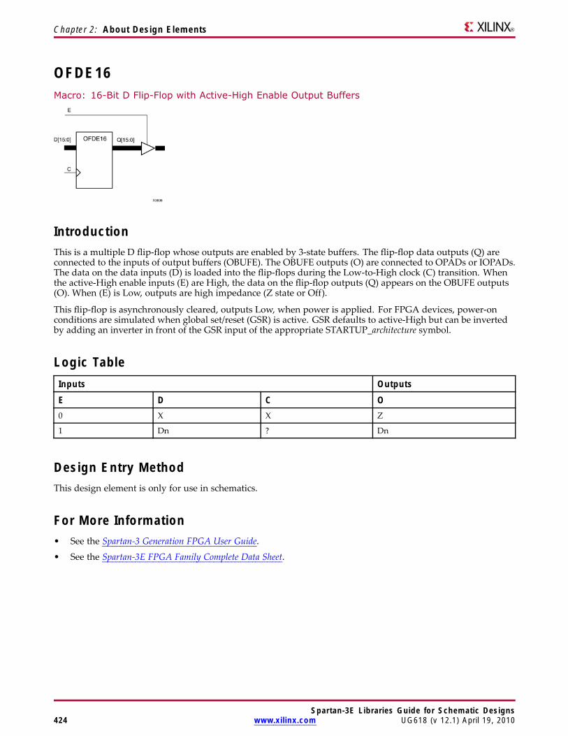
Chapter 2: About Design Elements
OFDE16Macro: 16-Bit D Flip-Flop with Active-High Enable Output Buffers
IntroductionThis is a multiple D flip-flop whose outputs are enabled by 3-state buffers. The flip-flop data outputs (Q) areconnected to the inputs of output buffers (OBUFE). The OBUFE outputs (O) are connected to OPADs or IOPADs.The data on the data inputs (D) is loaded into the flip-flops during the Low-to-High clock (C) transition. Whenthe active-High enable inputs (E) are High, the data on the flip-flop outputs (Q) appears on the OBUFE outputs(O). When (E) is Low, outputs are high impedance (Z state or Off).
This flip-flop is asynchronously cleared, outputs Low, when power is applied. For FPGA devices, power-onconditions are simulated when global set/reset (GSR) is active. GSR defaults to active-High but can be invertedby adding an inverter in front of the GSR input of the appropriate STARTUP_architecture symbol.
Logic TableInputs Outputs
E D C O0 X X Z
1 Dn ? Dn
Design Entry MethodThis design element is only for use in schematics.
For More Information• See the Spartan-3 Generation FPGA User Guide.
• See the Spartan-3E FPGA Family Complete Data Sheet.
Spartan-3E Libraries Guide for Schematic Designs424 www.xilinx.com UG618 (v 12.1) April 19, 2010
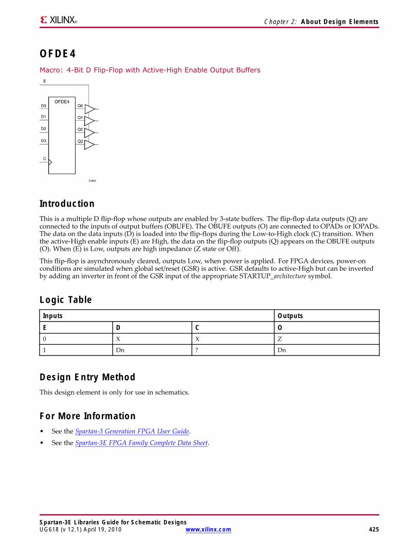
Chapter 2: About Design Elements
OFDE4Macro: 4-Bit D Flip-Flop with Active-High Enable Output Buffers
IntroductionThis is a multiple D flip-flop whose outputs are enabled by 3-state buffers. The flip-flop data outputs (Q) areconnected to the inputs of output buffers (OBUFE). The OBUFE outputs (O) are connected to OPADs or IOPADs.The data on the data inputs (D) is loaded into the flip-flops during the Low-to-High clock (C) transition. Whenthe active-High enable inputs (E) are High, the data on the flip-flop outputs (Q) appears on the OBUFE outputs(O). When (E) is Low, outputs are high impedance (Z state or Off).
This flip-flop is asynchronously cleared, outputs Low, when power is applied. For FPGA devices, power-onconditions are simulated when global set/reset (GSR) is active. GSR defaults to active-High but can be invertedby adding an inverter in front of the GSR input of the appropriate STARTUP_architecture symbol.
Logic TableInputs Outputs
E D C O0 X X Z
1 Dn ? Dn
Design Entry MethodThis design element is only for use in schematics.
For More Information• See the Spartan-3 Generation FPGA User Guide.
• See the Spartan-3E FPGA Family Complete Data Sheet.
Spartan-3E Libraries Guide for Schematic DesignsUG618 (v 12.1) April 19, 2010 www.xilinx.com 425
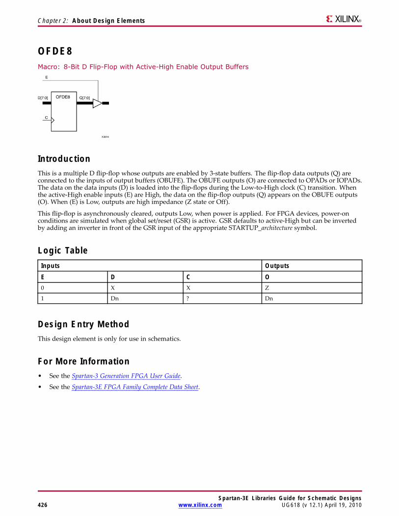
Chapter 2: About Design Elements
OFDE8Macro: 8-Bit D Flip-Flop with Active-High Enable Output Buffers
IntroductionThis is a multiple D flip-flop whose outputs are enabled by 3-state buffers. The flip-flop data outputs (Q) areconnected to the inputs of output buffers (OBUFE). The OBUFE outputs (O) are connected to OPADs or IOPADs.The data on the data inputs (D) is loaded into the flip-flops during the Low-to-High clock (C) transition. Whenthe active-High enable inputs (E) are High, the data on the flip-flop outputs (Q) appears on the OBUFE outputs(O). When (E) is Low, outputs are high impedance (Z state or Off).
This flip-flop is asynchronously cleared, outputs Low, when power is applied. For FPGA devices, power-onconditions are simulated when global set/reset (GSR) is active. GSR defaults to active-High but can be invertedby adding an inverter in front of the GSR input of the appropriate STARTUP_architecture symbol.
Logic TableInputs Outputs
E D C O0 X X Z
1 Dn ? Dn
Design Entry MethodThis design element is only for use in schematics.
For More Information• See the Spartan-3 Generation FPGA User Guide.
• See the Spartan-3E FPGA Family Complete Data Sheet.
Spartan-3E Libraries Guide for Schematic Designs426 www.xilinx.com UG618 (v 12.1) April 19, 2010
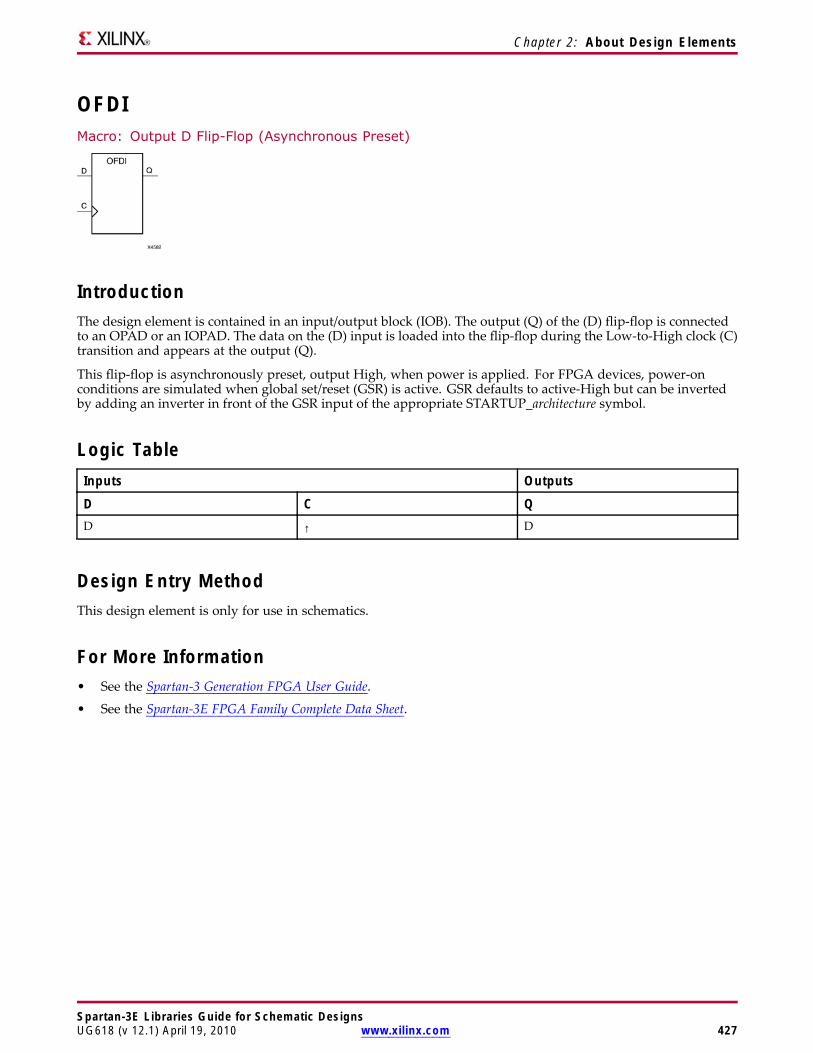
Chapter 2: About Design Elements
OFDIMacro: Output D Flip-Flop (Asynchronous Preset)
IntroductionThe design element is contained in an input/output block (IOB). The output (Q) of the (D) flip-flop is connectedto an OPAD or an IOPAD. The data on the (D) input is loaded into the flip-flop during the Low-to-High clock (C)transition and appears at the output (Q).
This flip-flop is asynchronously preset, output High, when power is applied. For FPGA devices, power-onconditions are simulated when global set/reset (GSR) is active. GSR defaults to active-High but can be invertedby adding an inverter in front of the GSR input of the appropriate STARTUP_architecture symbol.
Logic TableInputs Outputs
D C QD ↑ D
Design Entry MethodThis design element is only for use in schematics.
For More Information• See the Spartan-3 Generation FPGA User Guide.
• See the Spartan-3E FPGA Family Complete Data Sheet.
Spartan-3E Libraries Guide for Schematic DesignsUG618 (v 12.1) April 19, 2010 www.xilinx.com 427
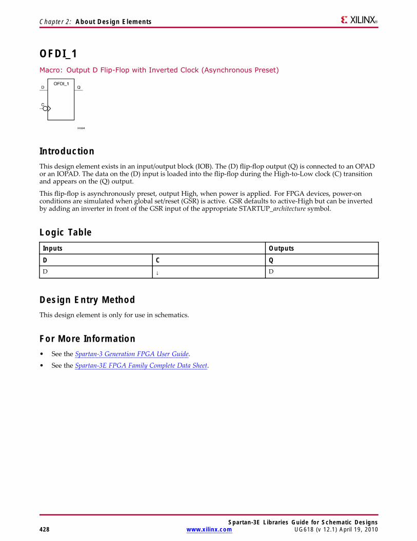
Chapter 2: About Design Elements
OFDI_1Macro: Output D Flip-Flop with Inverted Clock (Asynchronous Preset)
IntroductionThis design element exists in an input/output block (IOB). The (D) flip-flop output (Q) is connected to an OPADor an IOPAD. The data on the (D) input is loaded into the flip-flop during the High-to-Low clock (C) transitionand appears on the (Q) output.
This flip-flop is asynchronously preset, output High, when power is applied. For FPGA devices, power-onconditions are simulated when global set/reset (GSR) is active. GSR defaults to active-High but can be invertedby adding an inverter in front of the GSR input of the appropriate STARTUP_architecture symbol.
Logic TableInputs Outputs
D C QD ↓ D
Design Entry MethodThis design element is only for use in schematics.
For More Information• See the Spartan-3 Generation FPGA User Guide.
• See the Spartan-3E FPGA Family Complete Data Sheet.
Spartan-3E Libraries Guide for Schematic Designs428 www.xilinx.com UG618 (v 12.1) April 19, 2010
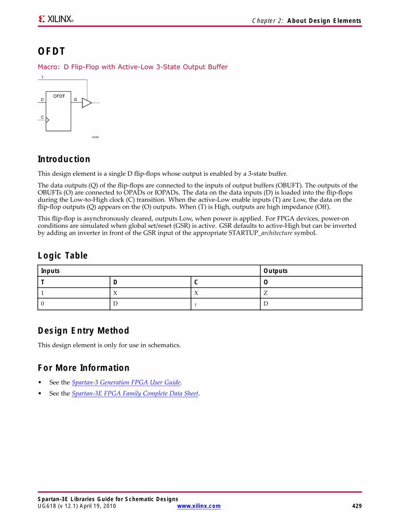
Chapter 2: About Design Elements
OFDTMacro: D Flip-Flop with Active-Low 3-State Output Buffer
IntroductionThis design element is a single D flip-flops whose output is enabled by a 3-state buffer.
The data outputs (Q) of the flip-flops are connected to the inputs of output buffers (OBUFT). The outputs of theOBUFTs (O) are connected to OPADs or IOPADs. The data on the data inputs (D) is loaded into the flip-flopsduring the Low-to-High clock (C) transition. When the active-Low enable inputs (T) are Low, the data on theflip-flop outputs (Q) appears on the (O) outputs. When (T) is High, outputs are high impedance (Off).
This flip-flop is asynchronously cleared, outputs Low, when power is applied. For FPGA devices, power-onconditions are simulated when global set/reset (GSR) is active. GSR defaults to active-High but can be invertedby adding an inverter in front of the GSR input of the appropriate STARTUP_architecture symbol.
Logic TableInputs Outputs
T D C O1 X X Z
0 D ↑ D
Design Entry MethodThis design element is only for use in schematics.
For More Information• See the Spartan-3 Generation FPGA User Guide.
• See the Spartan-3E FPGA Family Complete Data Sheet.
Spartan-3E Libraries Guide for Schematic DesignsUG618 (v 12.1) April 19, 2010 www.xilinx.com 429
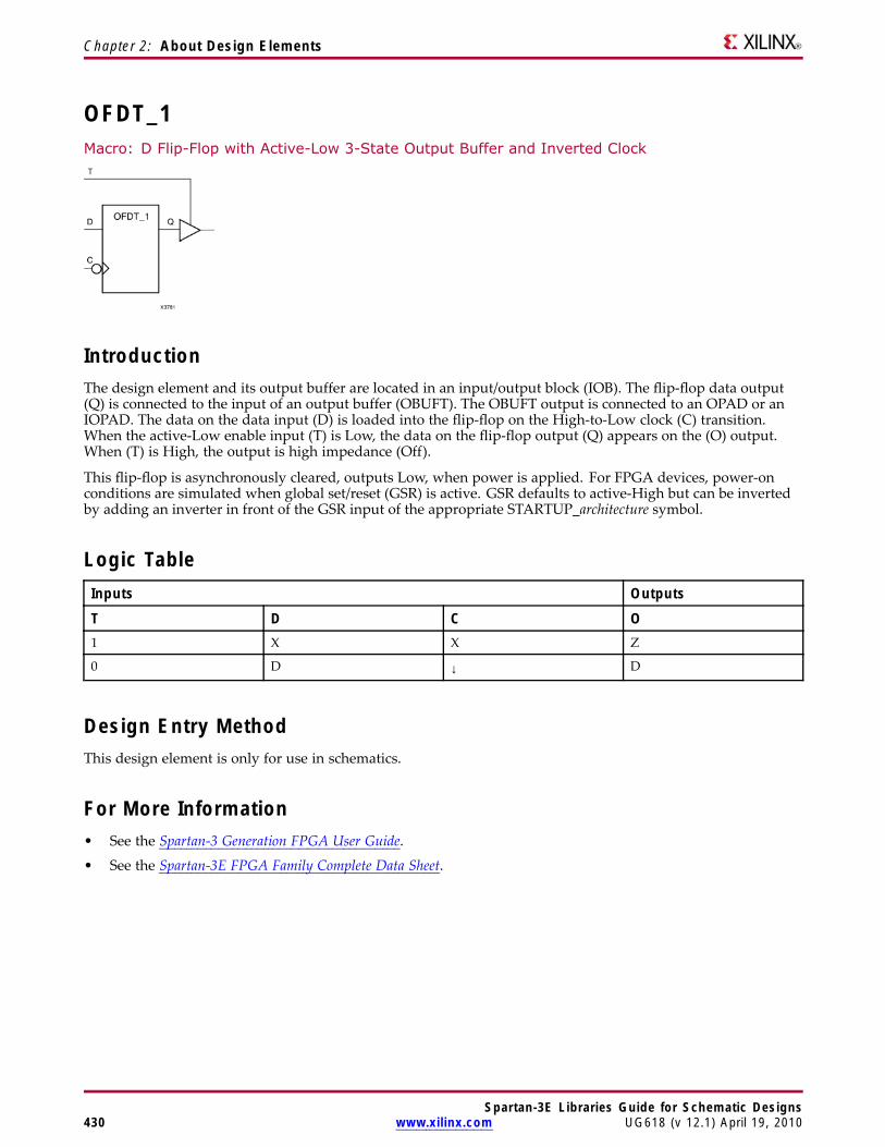
Chapter 2: About Design Elements
OFDT_1Macro: D Flip-Flop with Active-Low 3-State Output Buffer and Inverted Clock
IntroductionThe design element and its output buffer are located in an input/output block (IOB). The flip-flop data output(Q) is connected to the input of an output buffer (OBUFT). The OBUFT output is connected to an OPAD or anIOPAD. The data on the data input (D) is loaded into the flip-flop on the High-to-Low clock (C) transition.When the active-Low enable input (T) is Low, the data on the flip-flop output (Q) appears on the (O) output.When (T) is High, the output is high impedance (Off).
This flip-flop is asynchronously cleared, outputs Low, when power is applied. For FPGA devices, power-onconditions are simulated when global set/reset (GSR) is active. GSR defaults to active-High but can be invertedby adding an inverter in front of the GSR input of the appropriate STARTUP_architecture symbol.
Logic TableInputs Outputs
T D C O1 X X Z
0 D ↓ D
Design Entry MethodThis design element is only for use in schematics.
For More Information• See the Spartan-3 Generation FPGA User Guide.
• See the Spartan-3E FPGA Family Complete Data Sheet.
Spartan-3E Libraries Guide for Schematic Designs430 www.xilinx.com UG618 (v 12.1) April 19, 2010
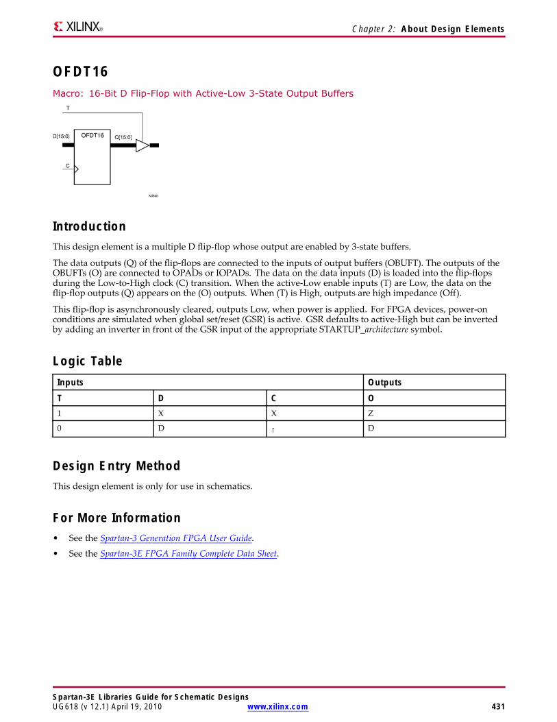
Chapter 2: About Design Elements
OFDT16Macro: 16-Bit D Flip-Flop with Active-Low 3-State Output Buffers
IntroductionThis design element is a multiple D flip-flop whose output are enabled by 3-state buffers.
The data outputs (Q) of the flip-flops are connected to the inputs of output buffers (OBUFT). The outputs of theOBUFTs (O) are connected to OPADs or IOPADs. The data on the data inputs (D) is loaded into the flip-flopsduring the Low-to-High clock (C) transition. When the active-Low enable inputs (T) are Low, the data on theflip-flop outputs (Q) appears on the (O) outputs. When (T) is High, outputs are high impedance (Off).
This flip-flop is asynchronously cleared, outputs Low, when power is applied. For FPGA devices, power-onconditions are simulated when global set/reset (GSR) is active. GSR defaults to active-High but can be invertedby adding an inverter in front of the GSR input of the appropriate STARTUP_architecture symbol.
Logic TableInputs Outputs
T D C O1 X X Z
0 D ↑ D
Design Entry MethodThis design element is only for use in schematics.
For More Information• See the Spartan-3 Generation FPGA User Guide.
• See the Spartan-3E FPGA Family Complete Data Sheet.
Spartan-3E Libraries Guide for Schematic DesignsUG618 (v 12.1) April 19, 2010 www.xilinx.com 431
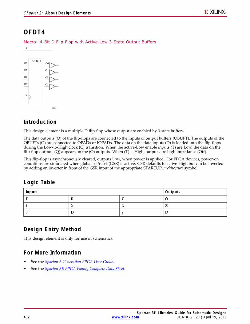
Chapter 2: About Design Elements
OFDT4Macro: 4-Bit D Flip-Flop with Active-Low 3-State Output Buffers
IntroductionThis design element is a multiple D flip-flop whose output are enabled by 3-state buffers.
The data outputs (Q) of the flip-flops are connected to the inputs of output buffers (OBUFT). The outputs of theOBUFTs (O) are connected to OPADs or IOPADs. The data on the data inputs (D) is loaded into the flip-flopsduring the Low-to-High clock (C) transition. When the active-Low enable inputs (T) are Low, the data on theflip-flop outputs (Q) appears on the (O) outputs. When (T) is High, outputs are high impedance (Off).
This flip-flop is asynchronously cleared, outputs Low, when power is applied. For FPGA devices, power-onconditions are simulated when global set/reset (GSR) is active. GSR defaults to active-High but can be invertedby adding an inverter in front of the GSR input of the appropriate STARTUP_architecture symbol.
Logic TableInputs Outputs
T D C O1 X X Z
0 D ↑ D
Design Entry MethodThis design element is only for use in schematics.
For More Information• See the Spartan-3 Generation FPGA User Guide.
• See the Spartan-3E FPGA Family Complete Data Sheet.
Spartan-3E Libraries Guide for Schematic Designs432 www.xilinx.com UG618 (v 12.1) April 19, 2010
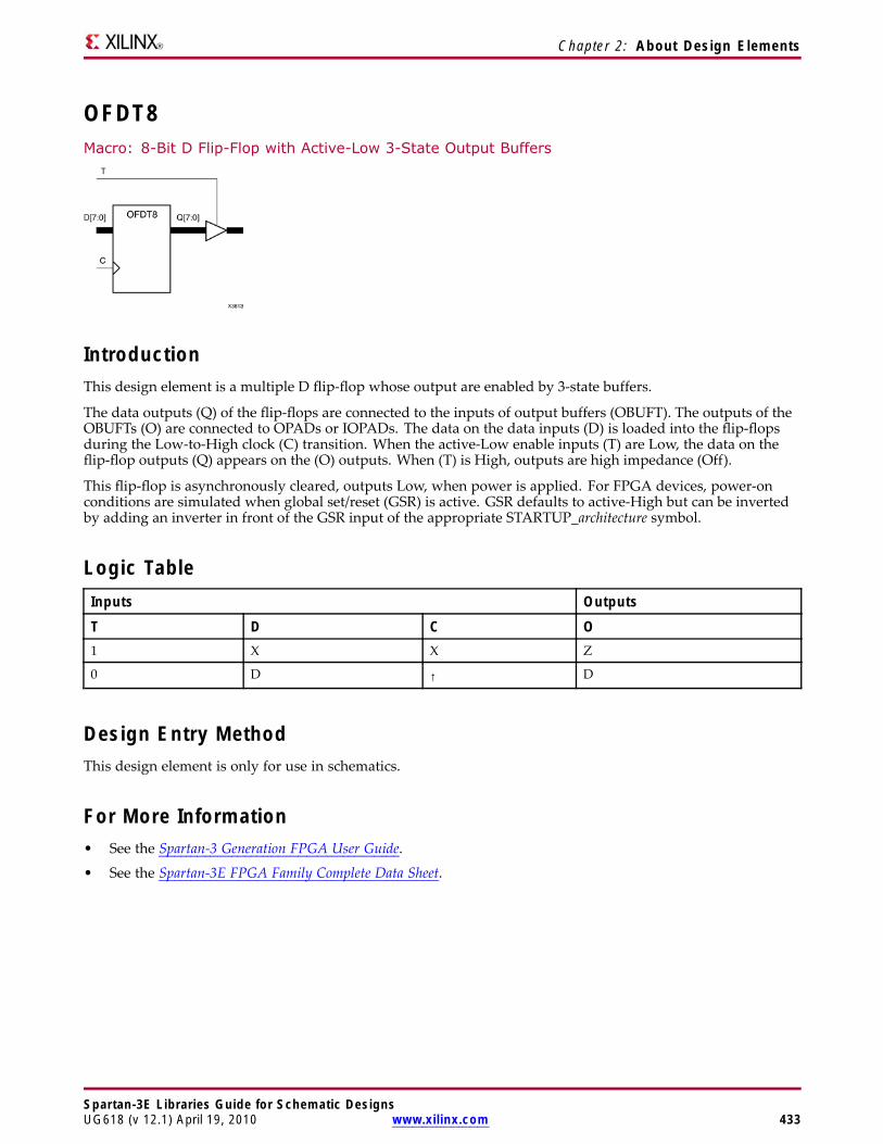
Chapter 2: About Design Elements
OFDT8Macro: 8-Bit D Flip-Flop with Active-Low 3-State Output Buffers
IntroductionThis design element is a multiple D flip-flop whose output are enabled by 3-state buffers.
The data outputs (Q) of the flip-flops are connected to the inputs of output buffers (OBUFT). The outputs of theOBUFTs (O) are connected to OPADs or IOPADs. The data on the data inputs (D) is loaded into the flip-flopsduring the Low-to-High clock (C) transition. When the active-Low enable inputs (T) are Low, the data on theflip-flop outputs (Q) appears on the (O) outputs. When (T) is High, outputs are high impedance (Off).
This flip-flop is asynchronously cleared, outputs Low, when power is applied. For FPGA devices, power-onconditions are simulated when global set/reset (GSR) is active. GSR defaults to active-High but can be invertedby adding an inverter in front of the GSR input of the appropriate STARTUP_architecture symbol.
Logic TableInputs Outputs
T D C O1 X X Z
0 D ↑ D
Design Entry MethodThis design element is only for use in schematics.
For More Information• See the Spartan-3 Generation FPGA User Guide.
• See the Spartan-3E FPGA Family Complete Data Sheet.
Spartan-3E Libraries Guide for Schematic DesignsUG618 (v 12.1) April 19, 2010 www.xilinx.com 433
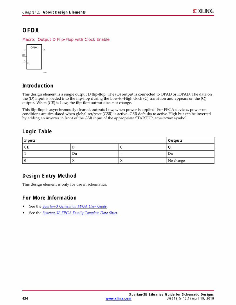
Chapter 2: About Design Elements
OFDXMacro: Output D Flip-Flop with Clock Enable
IntroductionThis design element is a single output D flip-flop. The (Q) output is connected to OPAD or IOPAD. The data onthe (D) input is loaded into the flip-flop during the Low-to-High clock (C) transition and appears on the (Q)output. When (CE) is Low, the flip-flop output does not change.
This flip-flop is asynchronously cleared, outputs Low, when power is applied. For FPGA devices, power-onconditions are simulated when global set/reset (GSR) is active. GSR defaults to active-High but can be invertedby adding an inverter in front of the GSR input of the appropriate STARTUP_architecture symbol.
Logic TableInputs Outputs
CE D C Q1 Dn ↑ Dn
0 X X No change
Design Entry MethodThis design element is only for use in schematics.
For More Information• See the Spartan-3 Generation FPGA User Guide.
• See the Spartan-3E FPGA Family Complete Data Sheet.
Spartan-3E Libraries Guide for Schematic Designs434 www.xilinx.com UG618 (v 12.1) April 19, 2010
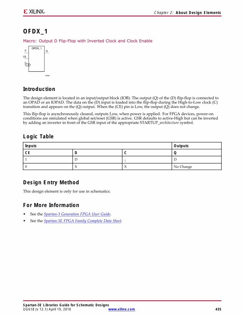
Chapter 2: About Design Elements
OFDX_1Macro: Output D Flip-Flop with Inverted Clock and Clock Enable
IntroductionThe design element is located in an input/output block (IOB). The output (Q) of the (D) flip-flop is connected toan OPAD or an IOPAD. The data on the (D) input is loaded into the flip-flop during the High-to-Low clock (C)transition and appears on the (Q) output. When the (CE) pin is Low, the output (Q) does not change.
This flip-flop is asynchronously cleared, outputs Low, when power is applied. For FPGA devices, power-onconditions are simulated when global set/reset (GSR) is active. GSR defaults to active-High but can be invertedby adding an inverter in front of the GSR input of the appropriate STARTUP_architecture symbol.
Logic TableInputs Outputs
CE D C Q1 D ↓ D
0 X X No Change
Design Entry MethodThis design element is only for use in schematics.
For More Information• See the Spartan-3 Generation FPGA User Guide.
• See the Spartan-3E FPGA Family Complete Data Sheet.
Spartan-3E Libraries Guide for Schematic DesignsUG618 (v 12.1) April 19, 2010 www.xilinx.com 435
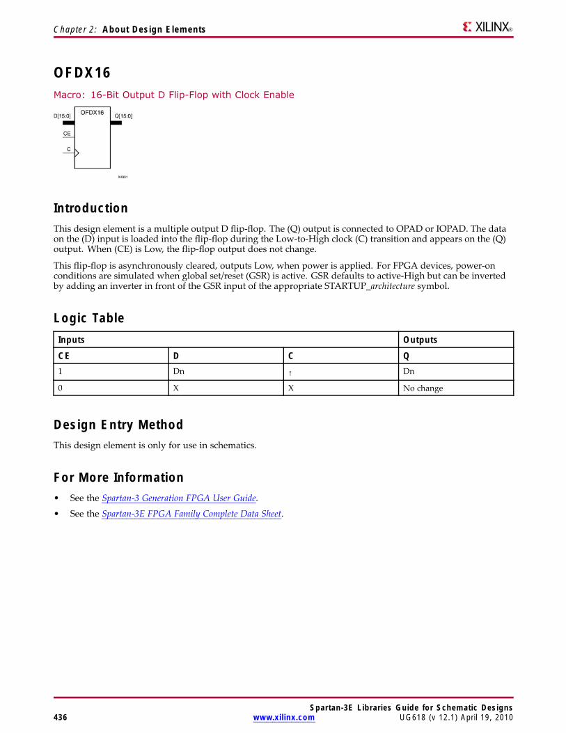
Chapter 2: About Design Elements
OFDX16Macro: 16-Bit Output D Flip-Flop with Clock Enable
IntroductionThis design element is a multiple output D flip-flop. The (Q) output is connected to OPAD or IOPAD. The dataon the (D) input is loaded into the flip-flop during the Low-to-High clock (C) transition and appears on the (Q)output. When (CE) is Low, the flip-flop output does not change.
This flip-flop is asynchronously cleared, outputs Low, when power is applied. For FPGA devices, power-onconditions are simulated when global set/reset (GSR) is active. GSR defaults to active-High but can be invertedby adding an inverter in front of the GSR input of the appropriate STARTUP_architecture symbol.
Logic TableInputs Outputs
CE D C Q1 Dn ↑ Dn
0 X X No change
Design Entry MethodThis design element is only for use in schematics.
For More Information• See the Spartan-3 Generation FPGA User Guide.
• See the Spartan-3E FPGA Family Complete Data Sheet.
Spartan-3E Libraries Guide for Schematic Designs436 www.xilinx.com UG618 (v 12.1) April 19, 2010
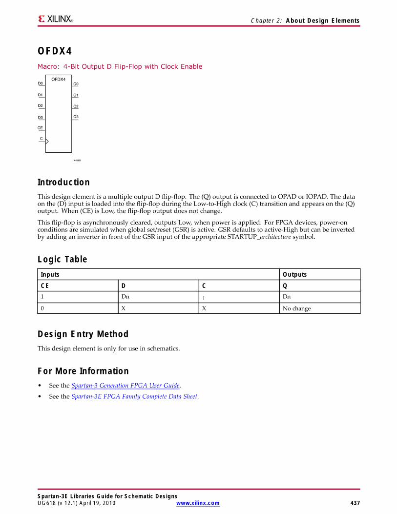
Chapter 2: About Design Elements
OFDX4Macro: 4-Bit Output D Flip-Flop with Clock Enable
IntroductionThis design element is a multiple output D flip-flop. The (Q) output is connected to OPAD or IOPAD. The dataon the (D) input is loaded into the flip-flop during the Low-to-High clock (C) transition and appears on the (Q)output. When (CE) is Low, the flip-flop output does not change.
This flip-flop is asynchronously cleared, outputs Low, when power is applied. For FPGA devices, power-onconditions are simulated when global set/reset (GSR) is active. GSR defaults to active-High but can be invertedby adding an inverter in front of the GSR input of the appropriate STARTUP_architecture symbol.
Logic TableInputs Outputs
CE D C Q1 Dn ↑ Dn
0 X X No change
Design Entry MethodThis design element is only for use in schematics.
For More Information• See the Spartan-3 Generation FPGA User Guide.
• See the Spartan-3E FPGA Family Complete Data Sheet.
Spartan-3E Libraries Guide for Schematic DesignsUG618 (v 12.1) April 19, 2010 www.xilinx.com 437
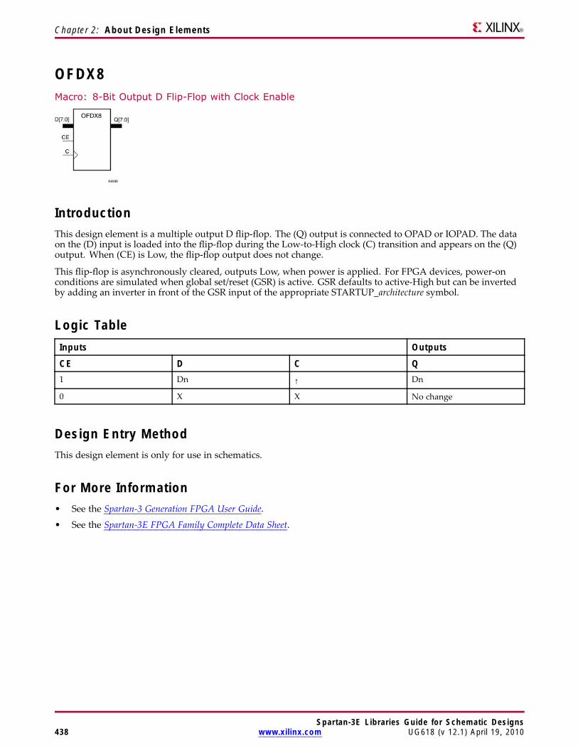
Chapter 2: About Design Elements
OFDX8Macro: 8-Bit Output D Flip-Flop with Clock Enable
IntroductionThis design element is a multiple output D flip-flop. The (Q) output is connected to OPAD or IOPAD. The dataon the (D) input is loaded into the flip-flop during the Low-to-High clock (C) transition and appears on the (Q)output. When (CE) is Low, the flip-flop output does not change.
This flip-flop is asynchronously cleared, outputs Low, when power is applied. For FPGA devices, power-onconditions are simulated when global set/reset (GSR) is active. GSR defaults to active-High but can be invertedby adding an inverter in front of the GSR input of the appropriate STARTUP_architecture symbol.
Logic TableInputs Outputs
CE D C Q1 Dn ↑ Dn
0 X X No change
Design Entry MethodThis design element is only for use in schematics.
For More Information• See the Spartan-3 Generation FPGA User Guide.
• See the Spartan-3E FPGA Family Complete Data Sheet.
Spartan-3E Libraries Guide for Schematic Designs438 www.xilinx.com UG618 (v 12.1) April 19, 2010
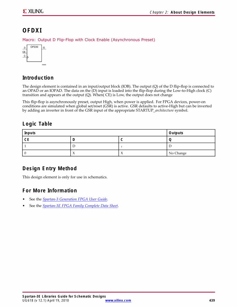
Chapter 2: About Design Elements
OFDXIMacro: Output D Flip-Flop with Clock Enable (Asynchronous Preset)
IntroductionThe design element is contained in an input/output block (IOB). The output (Q) of the D flip-flop is connected toan OPAD or an IOPAD. The data on the (D) input is loaded into the flip-flop during the Low-to-High clock (C)transition and appears at the output (Q). When( CE) is Low, the output does not change
This flip-flop is asynchronously preset, output High, when power is applied. For FPGA devices, power-onconditions are simulated when global set/reset (GSR) is active. GSR defaults to active-High but can be invertedby adding an inverter in front of the GSR input of the appropriate STARTUP_architecture symbol.
Logic TableInputs Outputs
CE D C Q1 D ↑ D
0 X X No Change
Design Entry MethodThis design element is only for use in schematics.
For More Information• See the Spartan-3 Generation FPGA User Guide.
• See the Spartan-3E FPGA Family Complete Data Sheet.
Spartan-3E Libraries Guide for Schematic DesignsUG618 (v 12.1) April 19, 2010 www.xilinx.com 439
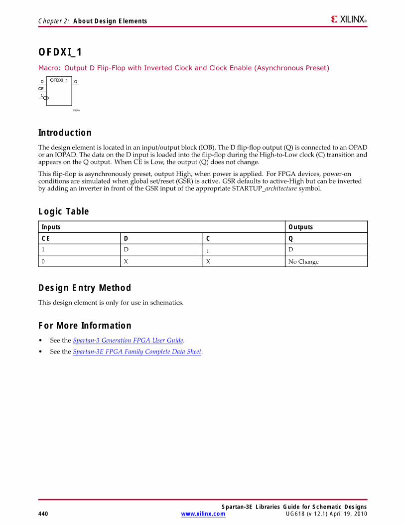
Chapter 2: About Design Elements
OFDXI_1Macro: Output D Flip-Flop with Inverted Clock and Clock Enable (Asynchronous Preset)
IntroductionThe design element is located in an input/output block (IOB). The D flip-flop output (Q) is connected to an OPADor an IOPAD. The data on the D input is loaded into the flip-flop during the High-to-Low clock (C) transition andappears on the Q output. When CE is Low, the output (Q) does not change.
This flip-flop is asynchronously preset, output High, when power is applied. For FPGA devices, power-onconditions are simulated when global set/reset (GSR) is active. GSR defaults to active-High but can be invertedby adding an inverter in front of the GSR input of the appropriate STARTUP_architecture symbol.
Logic TableInputs Outputs
CE D C Q1 D ↓ D
0 X X No Change
Design Entry MethodThis design element is only for use in schematics.
For More Information• See the Spartan-3 Generation FPGA User Guide.
• See the Spartan-3E FPGA Family Complete Data Sheet.
Spartan-3E Libraries Guide for Schematic Designs440 www.xilinx.com UG618 (v 12.1) April 19, 2010
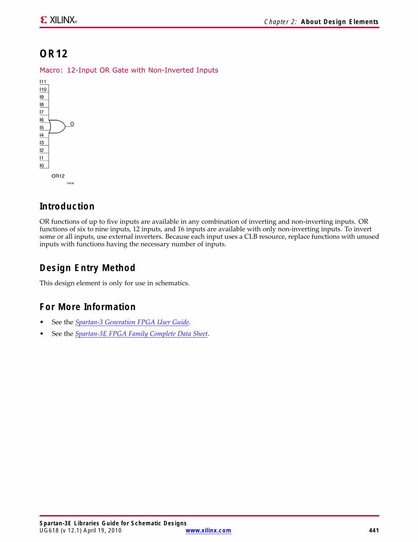
Chapter 2: About Design Elements
OR12Macro: 12-Input OR Gate with Non-Inverted Inputs
IntroductionOR functions of up to five inputs are available in any combination of inverting and non-inverting inputs. ORfunctions of six to nine inputs, 12 inputs, and 16 inputs are available with only non-inverting inputs. To invertsome or all inputs, use external inverters. Because each input uses a CLB resource, replace functions with unusedinputs with functions having the necessary number of inputs.
Design Entry MethodThis design element is only for use in schematics.
For More Information• See the Spartan-3 Generation FPGA User Guide.
• See the Spartan-3E FPGA Family Complete Data Sheet.
Spartan-3E Libraries Guide for Schematic DesignsUG618 (v 12.1) April 19, 2010 www.xilinx.com 441
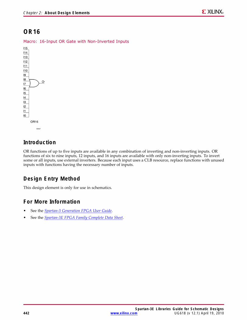
Chapter 2: About Design Elements
OR16Macro: 16-Input OR Gate with Non-Inverted Inputs
IntroductionOR functions of up to five inputs are available in any combination of inverting and non-inverting inputs. ORfunctions of six to nine inputs, 12 inputs, and 16 inputs are available with only non-inverting inputs. To invertsome or all inputs, use external inverters. Because each input uses a CLB resource, replace functions with unusedinputs with functions having the necessary number of inputs.
Design Entry MethodThis design element is only for use in schematics.
For More Information• See the Spartan-3 Generation FPGA User Guide.
• See the Spartan-3E FPGA Family Complete Data Sheet.
Spartan-3E Libraries Guide for Schematic Designs442 www.xilinx.com UG618 (v 12.1) April 19, 2010

Chapter 2: About Design Elements
OR2Primitive: 2-Input OR Gate with Non-Inverted Inputs
IntroductionOR functions of up to five inputs are available in any combination of inverting and non-inverting inputs. ORfunctions of six to nine inputs, 12 inputs, and 16 inputs are available with only non-inverting inputs. To invertsome or all inputs, use external inverters. Because each input uses a CLB resource, replace functions with unusedinputs with functions having the necessary number of inputs.
Design Entry MethodThis design element is only for use in schematics.
For More Information• See the Spartan-3 Generation FPGA User Guide.
• See the Spartan-3E FPGA Family Complete Data Sheet.
Spartan-3E Libraries Guide for Schematic DesignsUG618 (v 12.1) April 19, 2010 www.xilinx.com 443

Chapter 2: About Design Elements
OR2B1Primitive: 2-Input OR Gate with 1 Inverted and 1 Non-Inverted Inputs
IntroductionOR functions of up to five inputs are available in any combination of inverting and non-inverting inputs. ORfunctions of six to nine inputs, 12 inputs, and 16 inputs are available with only non-inverting inputs. To invertsome or all inputs, use external inverters. Because each input uses a CLB resource, replace functions with unusedinputs with functions having the necessary number of inputs.
Design Entry MethodThis design element is only for use in schematics.
For More Information• See the Spartan-3 Generation FPGA User Guide.
• See the Spartan-3E FPGA Family Complete Data Sheet.
Spartan-3E Libraries Guide for Schematic Designs444 www.xilinx.com UG618 (v 12.1) April 19, 2010
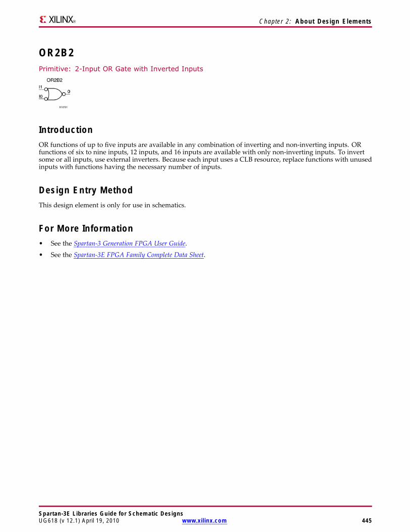
Chapter 2: About Design Elements
OR2B2Primitive: 2-Input OR Gate with Inverted Inputs
IntroductionOR functions of up to five inputs are available in any combination of inverting and non-inverting inputs. ORfunctions of six to nine inputs, 12 inputs, and 16 inputs are available with only non-inverting inputs. To invertsome or all inputs, use external inverters. Because each input uses a CLB resource, replace functions with unusedinputs with functions having the necessary number of inputs.
Design Entry MethodThis design element is only for use in schematics.
For More Information• See the Spartan-3 Generation FPGA User Guide.
• See the Spartan-3E FPGA Family Complete Data Sheet.
Spartan-3E Libraries Guide for Schematic DesignsUG618 (v 12.1) April 19, 2010 www.xilinx.com 445

Chapter 2: About Design Elements
OR3Primitive: 3-Input OR Gate with Non-Inverted Inputs
IntroductionOR functions of up to five inputs are available in any combination of inverting and non-inverting inputs. ORfunctions of six to nine inputs, 12 inputs, and 16 inputs are available with only non-inverting inputs. To invertsome or all inputs, use external inverters. Because each input uses a CLB resource, replace functions with unusedinputs with functions having the necessary number of inputs.
Design Entry MethodThis design element is only for use in schematics.
For More Information• See the Spartan-3 Generation FPGA User Guide.
• See the Spartan-3E FPGA Family Complete Data Sheet.
Spartan-3E Libraries Guide for Schematic Designs446 www.xilinx.com UG618 (v 12.1) April 19, 2010
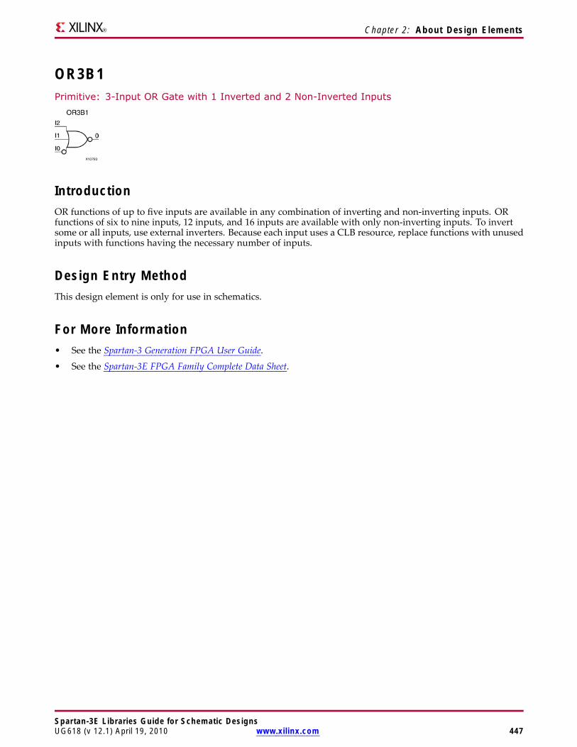
Chapter 2: About Design Elements
OR3B1Primitive: 3-Input OR Gate with 1 Inverted and 2 Non-Inverted Inputs
IntroductionOR functions of up to five inputs are available in any combination of inverting and non-inverting inputs. ORfunctions of six to nine inputs, 12 inputs, and 16 inputs are available with only non-inverting inputs. To invertsome or all inputs, use external inverters. Because each input uses a CLB resource, replace functions with unusedinputs with functions having the necessary number of inputs.
Design Entry MethodThis design element is only for use in schematics.
For More Information• See the Spartan-3 Generation FPGA User Guide.
• See the Spartan-3E FPGA Family Complete Data Sheet.
Spartan-3E Libraries Guide for Schematic DesignsUG618 (v 12.1) April 19, 2010 www.xilinx.com 447
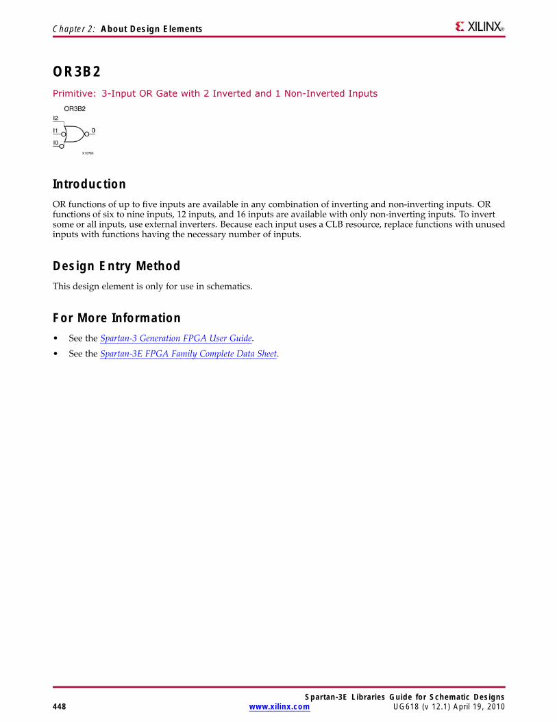
Chapter 2: About Design Elements
OR3B2Primitive: 3-Input OR Gate with 2 Inverted and 1 Non-Inverted Inputs
IntroductionOR functions of up to five inputs are available in any combination of inverting and non-inverting inputs. ORfunctions of six to nine inputs, 12 inputs, and 16 inputs are available with only non-inverting inputs. To invertsome or all inputs, use external inverters. Because each input uses a CLB resource, replace functions with unusedinputs with functions having the necessary number of inputs.
Design Entry MethodThis design element is only for use in schematics.
For More Information• See the Spartan-3 Generation FPGA User Guide.
• See the Spartan-3E FPGA Family Complete Data Sheet.
Spartan-3E Libraries Guide for Schematic Designs448 www.xilinx.com UG618 (v 12.1) April 19, 2010

Chapter 2: About Design Elements
OR3B3Primitive: 3-Input OR Gate with Inverted Inputs
IntroductionOR functions of up to five inputs are available in any combination of inverting and non-inverting inputs. ORfunctions of six to nine inputs, 12 inputs, and 16 inputs are available with only non-inverting inputs. To invertsome or all inputs, use external inverters. Because each input uses a CLB resource, replace functions with unusedinputs with functions having the necessary number of inputs.
Design Entry MethodThis design element is only for use in schematics.
For More Information• See the Spartan-3 Generation FPGA User Guide.
• See the Spartan-3E FPGA Family Complete Data Sheet.
Spartan-3E Libraries Guide for Schematic DesignsUG618 (v 12.1) April 19, 2010 www.xilinx.com 449
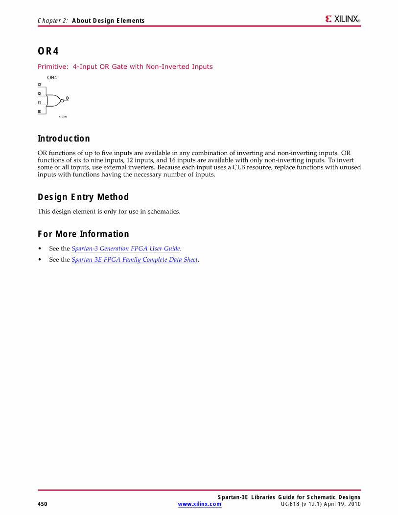
Chapter 2: About Design Elements
OR4Primitive: 4-Input OR Gate with Non-Inverted Inputs
IntroductionOR functions of up to five inputs are available in any combination of inverting and non-inverting inputs. ORfunctions of six to nine inputs, 12 inputs, and 16 inputs are available with only non-inverting inputs. To invertsome or all inputs, use external inverters. Because each input uses a CLB resource, replace functions with unusedinputs with functions having the necessary number of inputs.
Design Entry MethodThis design element is only for use in schematics.
For More Information• See the Spartan-3 Generation FPGA User Guide.
• See the Spartan-3E FPGA Family Complete Data Sheet.
Spartan-3E Libraries Guide for Schematic Designs450 www.xilinx.com UG618 (v 12.1) April 19, 2010

Chapter 2: About Design Elements
OR4B1Primitive: 4-Input OR Gate with 1 Inverted and 3 Non-Inverted Inputs
IntroductionOR functions of up to five inputs are available in any combination of inverting and non-inverting inputs. ORfunctions of six to nine inputs, 12 inputs, and 16 inputs are available with only non-inverting inputs. To invertsome or all inputs, use external inverters. Because each input uses a CLB resource, replace functions with unusedinputs with functions having the necessary number of inputs.
Design Entry MethodThis design element is only for use in schematics.
For More Information• See the Spartan-3 Generation FPGA User Guide.
• See the Spartan-3E FPGA Family Complete Data Sheet.
Spartan-3E Libraries Guide for Schematic DesignsUG618 (v 12.1) April 19, 2010 www.xilinx.com 451
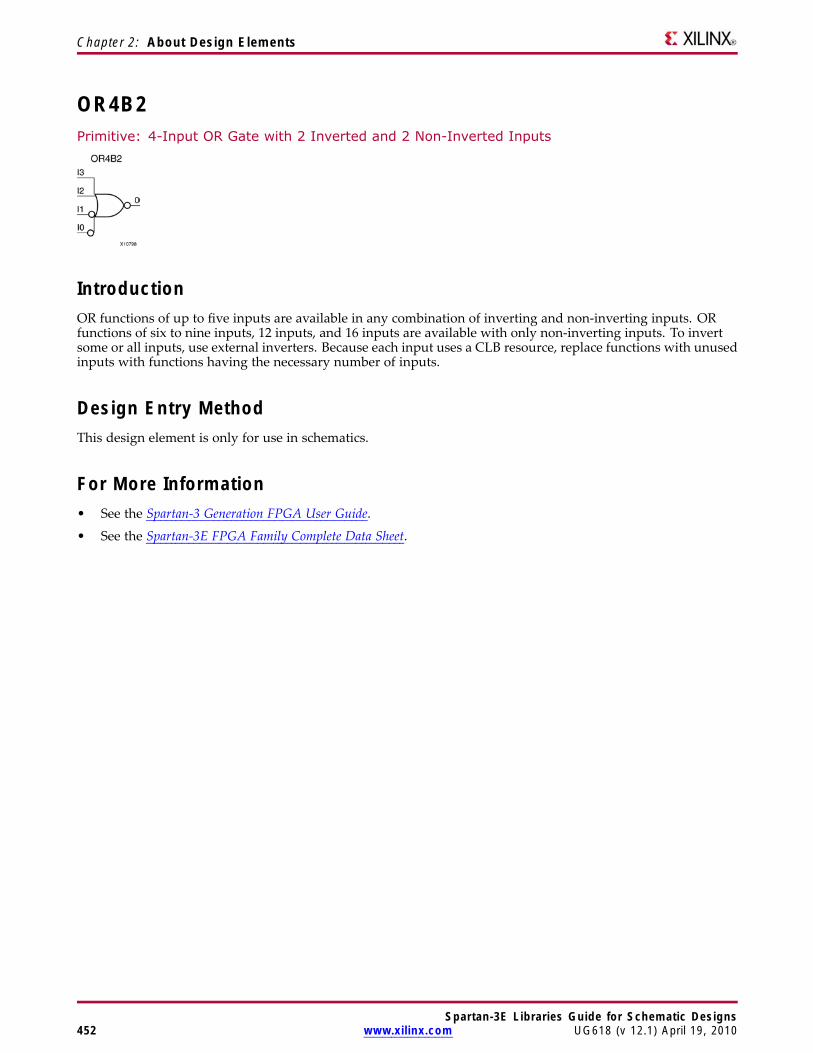
Chapter 2: About Design Elements
OR4B2Primitive: 4-Input OR Gate with 2 Inverted and 2 Non-Inverted Inputs
IntroductionOR functions of up to five inputs are available in any combination of inverting and non-inverting inputs. ORfunctions of six to nine inputs, 12 inputs, and 16 inputs are available with only non-inverting inputs. To invertsome or all inputs, use external inverters. Because each input uses a CLB resource, replace functions with unusedinputs with functions having the necessary number of inputs.
Design Entry MethodThis design element is only for use in schematics.
For More Information• See the Spartan-3 Generation FPGA User Guide.
• See the Spartan-3E FPGA Family Complete Data Sheet.
Spartan-3E Libraries Guide for Schematic Designs452 www.xilinx.com UG618 (v 12.1) April 19, 2010
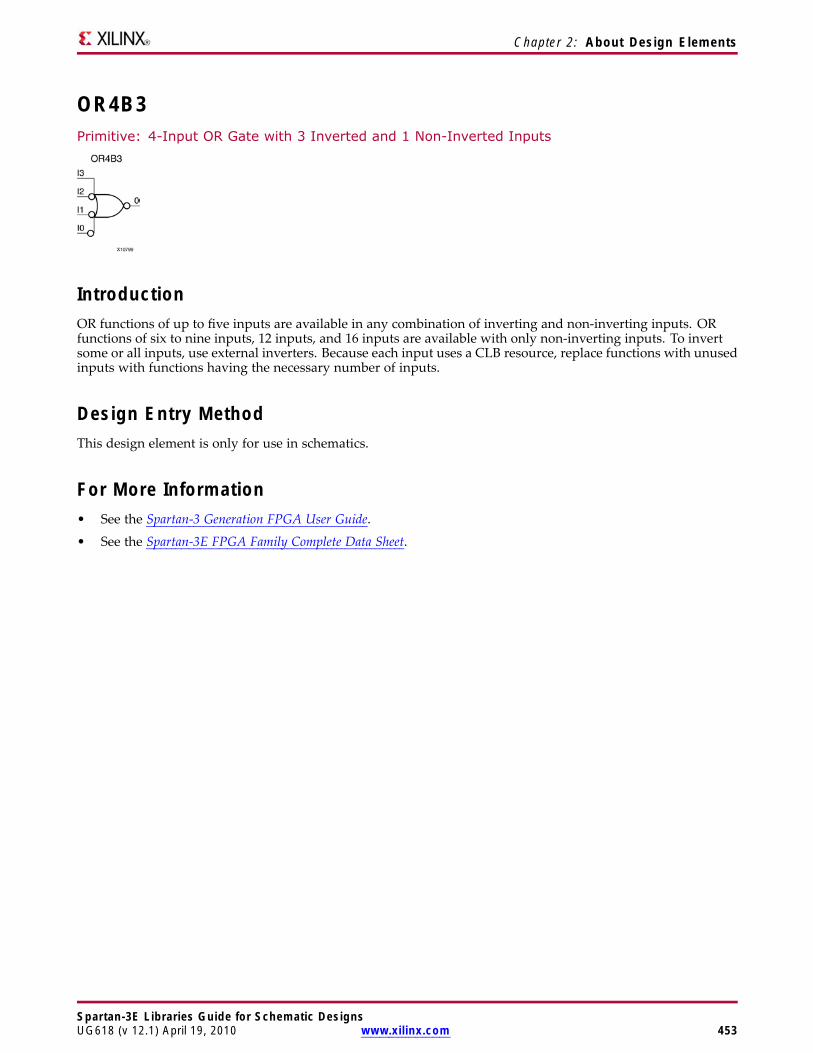
Chapter 2: About Design Elements
OR4B3Primitive: 4-Input OR Gate with 3 Inverted and 1 Non-Inverted Inputs
IntroductionOR functions of up to five inputs are available in any combination of inverting and non-inverting inputs. ORfunctions of six to nine inputs, 12 inputs, and 16 inputs are available with only non-inverting inputs. To invertsome or all inputs, use external inverters. Because each input uses a CLB resource, replace functions with unusedinputs with functions having the necessary number of inputs.
Design Entry MethodThis design element is only for use in schematics.
For More Information• See the Spartan-3 Generation FPGA User Guide.
• See the Spartan-3E FPGA Family Complete Data Sheet.
Spartan-3E Libraries Guide for Schematic DesignsUG618 (v 12.1) April 19, 2010 www.xilinx.com 453
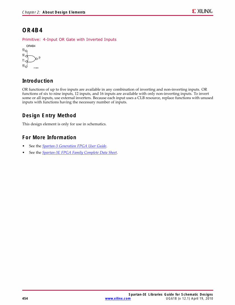
Chapter 2: About Design Elements
OR4B4Primitive: 4-Input OR Gate with Inverted Inputs
IntroductionOR functions of up to five inputs are available in any combination of inverting and non-inverting inputs. ORfunctions of six to nine inputs, 12 inputs, and 16 inputs are available with only non-inverting inputs. To invertsome or all inputs, use external inverters. Because each input uses a CLB resource, replace functions with unusedinputs with functions having the necessary number of inputs.
Design Entry MethodThis design element is only for use in schematics.
For More Information• See the Spartan-3 Generation FPGA User Guide.
• See the Spartan-3E FPGA Family Complete Data Sheet.
Spartan-3E Libraries Guide for Schematic Designs454 www.xilinx.com UG618 (v 12.1) April 19, 2010
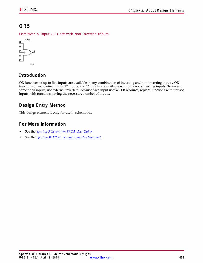
Chapter 2: About Design Elements
OR5Primitive: 5-Input OR Gate with Non-Inverted Inputs
IntroductionOR functions of up to five inputs are available in any combination of inverting and non-inverting inputs. ORfunctions of six to nine inputs, 12 inputs, and 16 inputs are available with only non-inverting inputs. To invertsome or all inputs, use external inverters. Because each input uses a CLB resource, replace functions with unusedinputs with functions having the necessary number of inputs.
Design Entry MethodThis design element is only for use in schematics.
For More Information• See the Spartan-3 Generation FPGA User Guide.
• See the Spartan-3E FPGA Family Complete Data Sheet.
Spartan-3E Libraries Guide for Schematic DesignsUG618 (v 12.1) April 19, 2010 www.xilinx.com 455
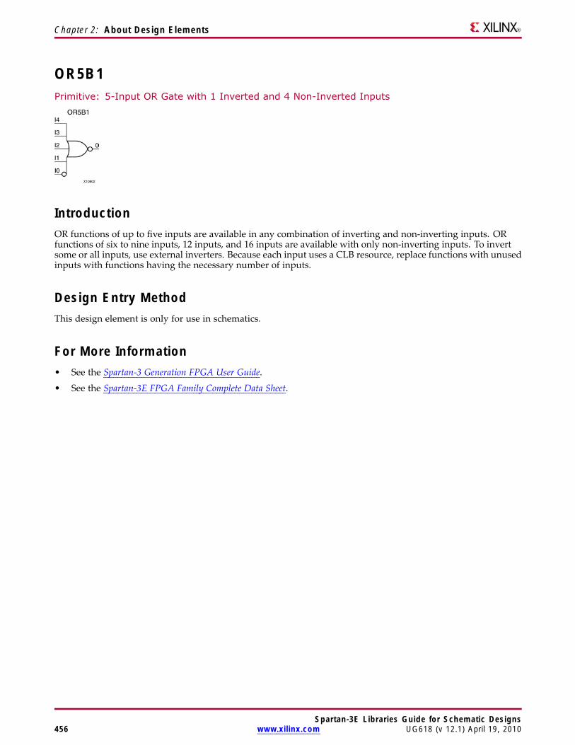
Chapter 2: About Design Elements
OR5B1Primitive: 5-Input OR Gate with 1 Inverted and 4 Non-Inverted Inputs
IntroductionOR functions of up to five inputs are available in any combination of inverting and non-inverting inputs. ORfunctions of six to nine inputs, 12 inputs, and 16 inputs are available with only non-inverting inputs. To invertsome or all inputs, use external inverters. Because each input uses a CLB resource, replace functions with unusedinputs with functions having the necessary number of inputs.
Design Entry MethodThis design element is only for use in schematics.
For More Information• See the Spartan-3 Generation FPGA User Guide.
• See the Spartan-3E FPGA Family Complete Data Sheet.
Spartan-3E Libraries Guide for Schematic Designs456 www.xilinx.com UG618 (v 12.1) April 19, 2010
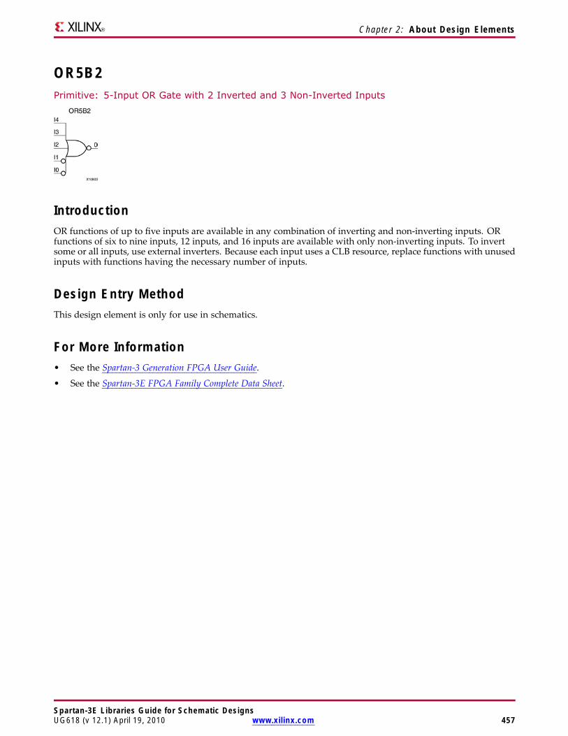
Chapter 2: About Design Elements
OR5B2Primitive: 5-Input OR Gate with 2 Inverted and 3 Non-Inverted Inputs
IntroductionOR functions of up to five inputs are available in any combination of inverting and non-inverting inputs. ORfunctions of six to nine inputs, 12 inputs, and 16 inputs are available with only non-inverting inputs. To invertsome or all inputs, use external inverters. Because each input uses a CLB resource, replace functions with unusedinputs with functions having the necessary number of inputs.
Design Entry MethodThis design element is only for use in schematics.
For More Information• See the Spartan-3 Generation FPGA User Guide.
• See the Spartan-3E FPGA Family Complete Data Sheet.
Spartan-3E Libraries Guide for Schematic DesignsUG618 (v 12.1) April 19, 2010 www.xilinx.com 457

Chapter 2: About Design Elements
OR5B3Primitive: 5-Input OR Gate with 3 Inverted and 2 Non-Inverted Inputs
IntroductionOR functions of up to five inputs are available in any combination of inverting and non-inverting inputs. ORfunctions of six to nine inputs, 12 inputs, and 16 inputs are available with only non-inverting inputs. To invertsome or all inputs, use external inverters. Because each input uses a CLB resource, replace functions with unusedinputs with functions having the necessary number of inputs.
Design Entry MethodThis design element is only for use in schematics.
For More Information• See the Spartan-3 Generation FPGA User Guide.
• See the Spartan-3E FPGA Family Complete Data Sheet.
Spartan-3E Libraries Guide for Schematic Designs458 www.xilinx.com UG618 (v 12.1) April 19, 2010

Chapter 2: About Design Elements
OR5B4Primitive: 5-Input OR Gate with 4 Inverted and 1 Non-Inverted Inputs
IntroductionOR functions of up to five inputs are available in any combination of inverting and non-inverting inputs. ORfunctions of six to nine inputs, 12 inputs, and 16 inputs are available with only non-inverting inputs. To invertsome or all inputs, use external inverters. Because each input uses a CLB resource, replace functions with unusedinputs with functions having the necessary number of inputs.
Design Entry MethodThis design element is only for use in schematics.
For More Information• See the Spartan-3 Generation FPGA User Guide.
• See the Spartan-3E FPGA Family Complete Data Sheet.
Spartan-3E Libraries Guide for Schematic DesignsUG618 (v 12.1) April 19, 2010 www.xilinx.com 459
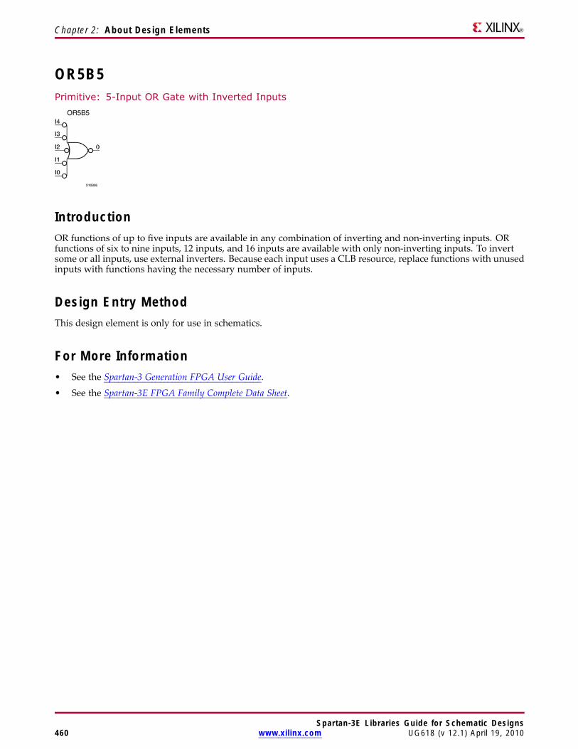
Chapter 2: About Design Elements
OR5B5Primitive: 5-Input OR Gate with Inverted Inputs
IntroductionOR functions of up to five inputs are available in any combination of inverting and non-inverting inputs. ORfunctions of six to nine inputs, 12 inputs, and 16 inputs are available with only non-inverting inputs. To invertsome or all inputs, use external inverters. Because each input uses a CLB resource, replace functions with unusedinputs with functions having the necessary number of inputs.
Design Entry MethodThis design element is only for use in schematics.
For More Information• See the Spartan-3 Generation FPGA User Guide.
• See the Spartan-3E FPGA Family Complete Data Sheet.
Spartan-3E Libraries Guide for Schematic Designs460 www.xilinx.com UG618 (v 12.1) April 19, 2010
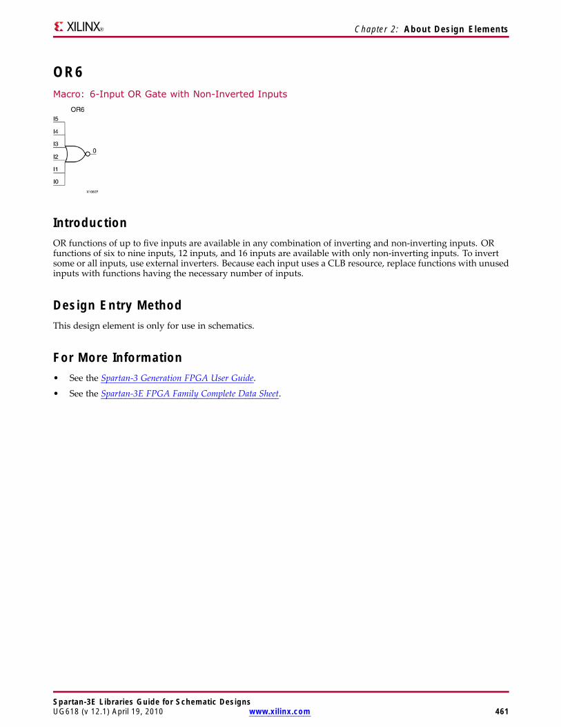
Chapter 2: About Design Elements
OR6Macro: 6-Input OR Gate with Non-Inverted Inputs
IntroductionOR functions of up to five inputs are available in any combination of inverting and non-inverting inputs. ORfunctions of six to nine inputs, 12 inputs, and 16 inputs are available with only non-inverting inputs. To invertsome or all inputs, use external inverters. Because each input uses a CLB resource, replace functions with unusedinputs with functions having the necessary number of inputs.
Design Entry MethodThis design element is only for use in schematics.
For More Information• See the Spartan-3 Generation FPGA User Guide.
• See the Spartan-3E FPGA Family Complete Data Sheet.
Spartan-3E Libraries Guide for Schematic DesignsUG618 (v 12.1) April 19, 2010 www.xilinx.com 461
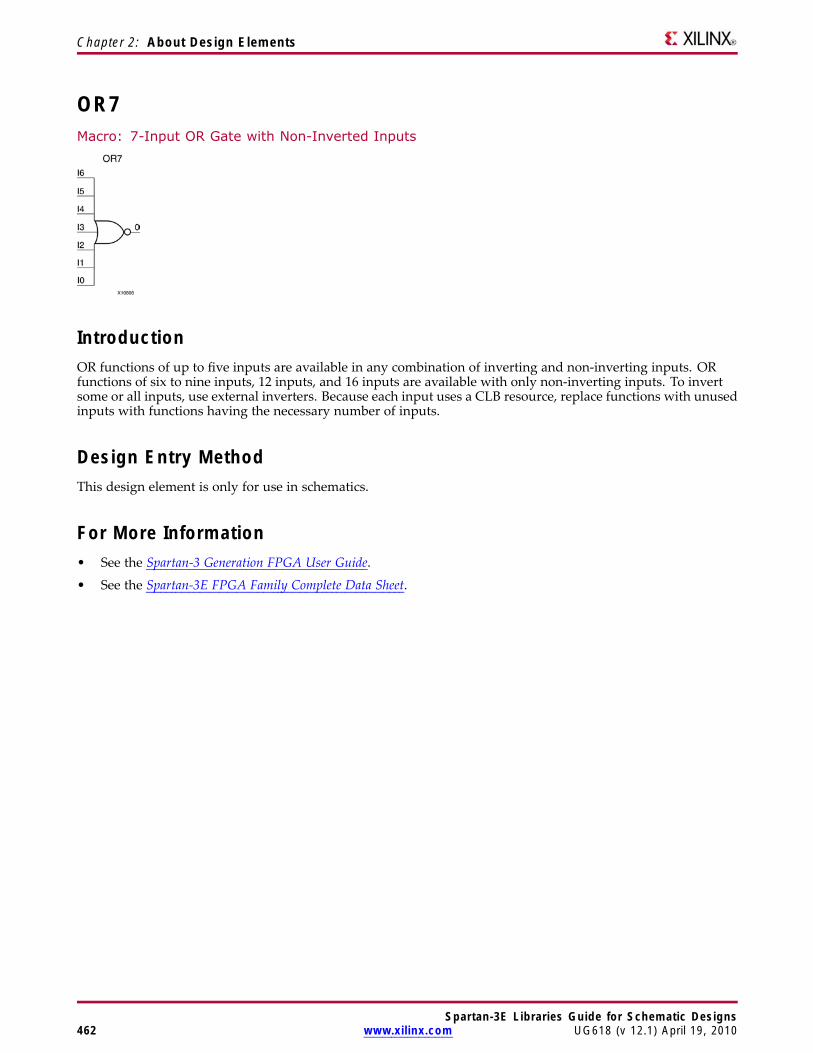
Chapter 2: About Design Elements
OR7Macro: 7-Input OR Gate with Non-Inverted Inputs
IntroductionOR functions of up to five inputs are available in any combination of inverting and non-inverting inputs. ORfunctions of six to nine inputs, 12 inputs, and 16 inputs are available with only non-inverting inputs. To invertsome or all inputs, use external inverters. Because each input uses a CLB resource, replace functions with unusedinputs with functions having the necessary number of inputs.
Design Entry MethodThis design element is only for use in schematics.
For More Information• See the Spartan-3 Generation FPGA User Guide.
• See the Spartan-3E FPGA Family Complete Data Sheet.
Spartan-3E Libraries Guide for Schematic Designs462 www.xilinx.com UG618 (v 12.1) April 19, 2010
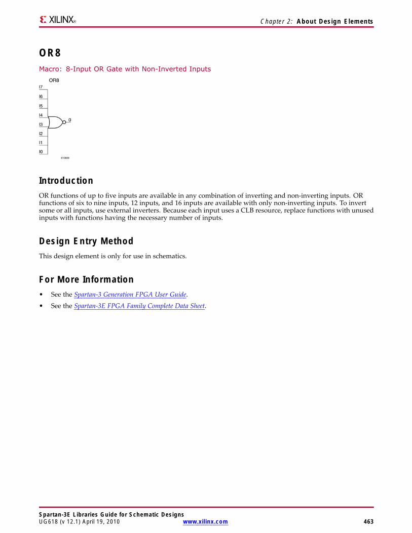
Chapter 2: About Design Elements
OR8Macro: 8-Input OR Gate with Non-Inverted Inputs
IntroductionOR functions of up to five inputs are available in any combination of inverting and non-inverting inputs. ORfunctions of six to nine inputs, 12 inputs, and 16 inputs are available with only non-inverting inputs. To invertsome or all inputs, use external inverters. Because each input uses a CLB resource, replace functions with unusedinputs with functions having the necessary number of inputs.
Design Entry MethodThis design element is only for use in schematics.
For More Information• See the Spartan-3 Generation FPGA User Guide.
• See the Spartan-3E FPGA Family Complete Data Sheet.
Spartan-3E Libraries Guide for Schematic DesignsUG618 (v 12.1) April 19, 2010 www.xilinx.com 463
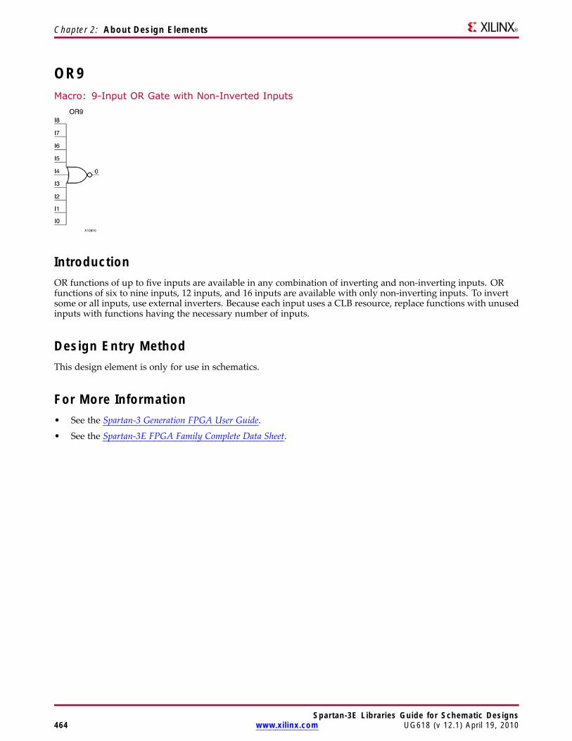
Chapter 2: About Design Elements
OR9Macro: 9-Input OR Gate with Non-Inverted Inputs
IntroductionOR functions of up to five inputs are available in any combination of inverting and non-inverting inputs. ORfunctions of six to nine inputs, 12 inputs, and 16 inputs are available with only non-inverting inputs. To invertsome or all inputs, use external inverters. Because each input uses a CLB resource, replace functions with unusedinputs with functions having the necessary number of inputs.
Design Entry MethodThis design element is only for use in schematics.
For More Information• See the Spartan-3 Generation FPGA User Guide.
• See the Spartan-3E FPGA Family Complete Data Sheet.
Spartan-3E Libraries Guide for Schematic Designs464 www.xilinx.com UG618 (v 12.1) April 19, 2010
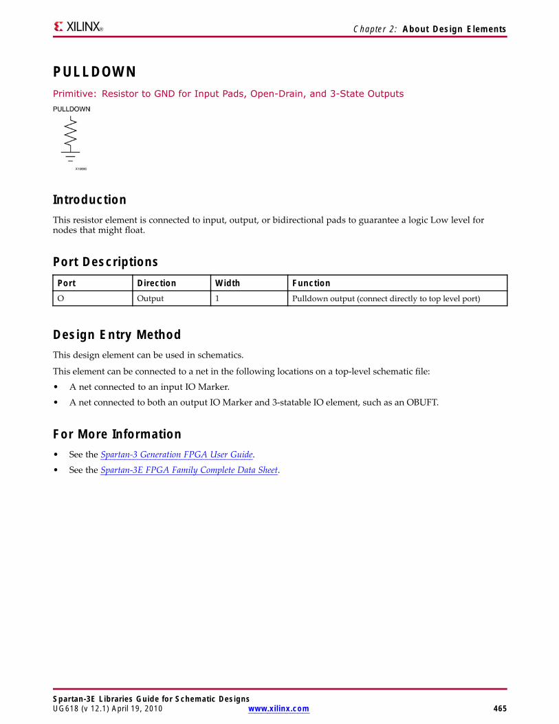
Chapter 2: About Design Elements
PULLDOWNPrimitive: Resistor to GND for Input Pads, Open-Drain, and 3-State Outputs
IntroductionThis resistor element is connected to input, output, or bidirectional pads to guarantee a logic Low level fornodes that might float.
Port DescriptionsPort Direction Width FunctionO Output 1 Pulldown output (connect directly to top level port)
Design Entry MethodThis design element can be used in schematics.
This element can be connected to a net in the following locations on a top-level schematic file:
• A net connected to an input IO Marker.
• A net connected to both an output IO Marker and 3-statable IO element, such as an OBUFT.
For More Information• See the Spartan-3 Generation FPGA User Guide.
• See the Spartan-3E FPGA Family Complete Data Sheet.
Spartan-3E Libraries Guide for Schematic DesignsUG618 (v 12.1) April 19, 2010 www.xilinx.com 465
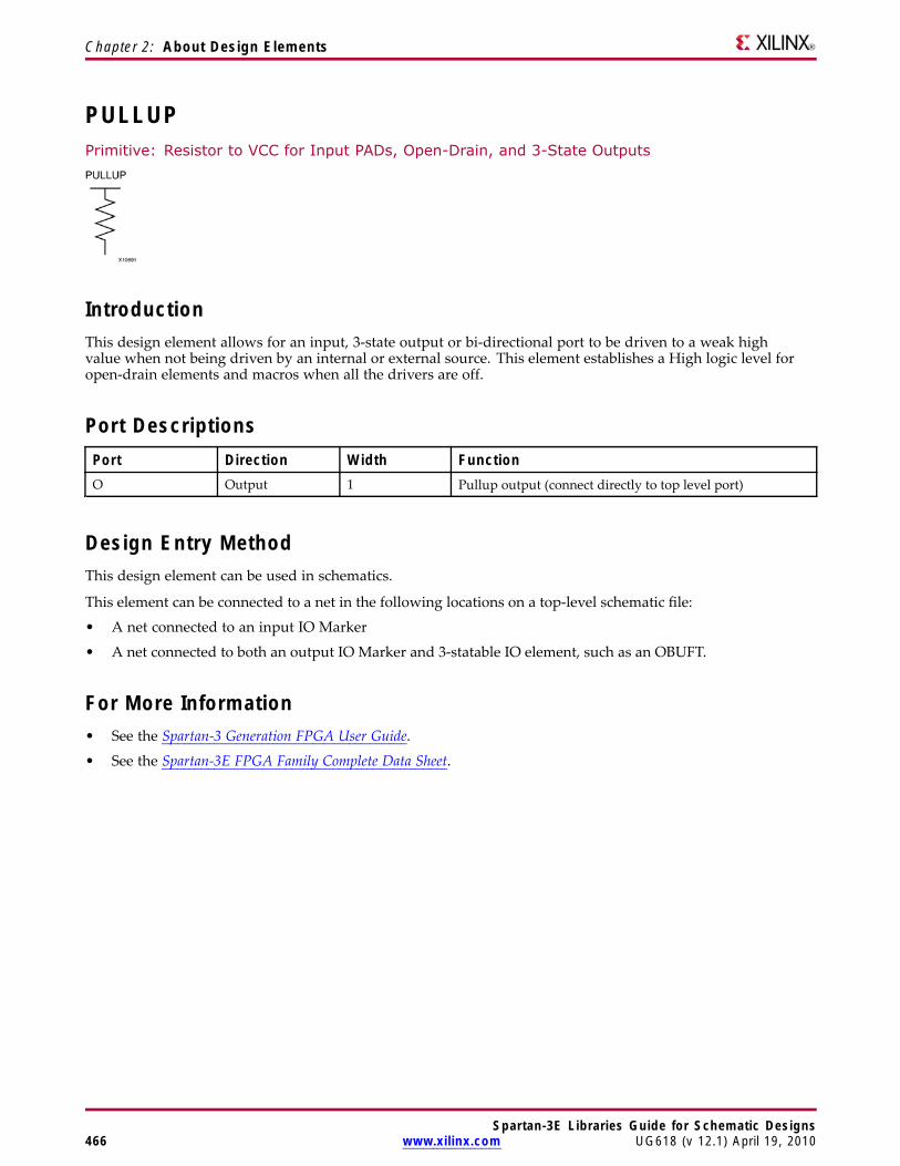
Chapter 2: About Design Elements
PULLUPPrimitive: Resistor to VCC for Input PADs, Open-Drain, and 3-State Outputs
IntroductionThis design element allows for an input, 3-state output or bi-directional port to be driven to a weak highvalue when not being driven by an internal or external source. This element establishes a High logic level foropen-drain elements and macros when all the drivers are off.
Port DescriptionsPort Direction Width FunctionO Output 1 Pullup output (connect directly to top level port)
Design Entry MethodThis design element can be used in schematics.
This element can be connected to a net in the following locations on a top-level schematic file:
• A net connected to an input IO Marker
• A net connected to both an output IO Marker and 3-statable IO element, such as an OBUFT.
For More Information• See the Spartan-3 Generation FPGA User Guide.
• See the Spartan-3E FPGA Family Complete Data Sheet.
Spartan-3E Libraries Guide for Schematic Designs466 www.xilinx.com UG618 (v 12.1) April 19, 2010
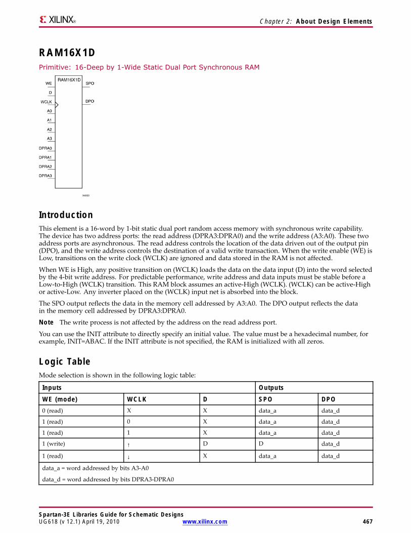
Chapter 2: About Design Elements
RAM16X1DPrimitive: 16-Deep by 1-Wide Static Dual Port Synchronous RAM
IntroductionThis element is a 16-word by 1-bit static dual port random access memory with synchronous write capability.The device has two address ports: the read address (DPRA3:DPRA0) and the write address (A3:A0). These twoaddress ports are asynchronous. The read address controls the location of the data driven out of the output pin(DPO), and the write address controls the destination of a valid write transaction. When the write enable (WE) isLow, transitions on the write clock (WCLK) are ignored and data stored in the RAM is not affected.
When WE is High, any positive transition on (WCLK) loads the data on the data input (D) into the word selectedby the 4-bit write address. For predictable performance, write address and data inputs must be stable before aLow-to-High (WCLK) transition. This RAM block assumes an active-High (WCLK). (WCLK) can be active-Highor active-Low. Any inverter placed on the (WCLK) input net is absorbed into the block.
The SPO output reflects the data in the memory cell addressed by A3:A0. The DPO output reflects the datain the memory cell addressed by DPRA3:DPRA0.
Note The write process is not affected by the address on the read address port.
You can use the INIT attribute to directly specify an initial value. The value must be a hexadecimal number, forexample, INIT=ABAC. If the INIT attribute is not specified, the RAM is initialized with all zeros.
Logic TableMode selection is shown in the following logic table:
Inputs Outputs
WE (mode) WCLK D SPO DPO0 (read) X X data_a data_d
1 (read) 0 X data_a data_d
1 (read) 1 X data_a data_d
1 (write) ↑ D D data_d
1 (read) ↓ X data_a data_d
data_a = word addressed by bits A3-A0
data_d = word addressed by bits DPRA3-DPRA0
Spartan-3E Libraries Guide for Schematic DesignsUG618 (v 12.1) April 19, 2010 www.xilinx.com 467
Chapter 2: About Design Elements
Design Entry MethodThis design element can be used in schematics.
Available AttributesAttribute Type Allowed Values Default DescriptionINIT Hexadecimal Any 16-Bit Value All
zeros.Initializes RAMs, registers, and look-uptables.
For More Information• See the Spartan-3 Generation FPGA User Guide.
• See the Spartan-3E FPGA Family Complete Data Sheet.
Spartan-3E Libraries Guide for Schematic Designs468 www.xilinx.com UG618 (v 12.1) April 19, 2010
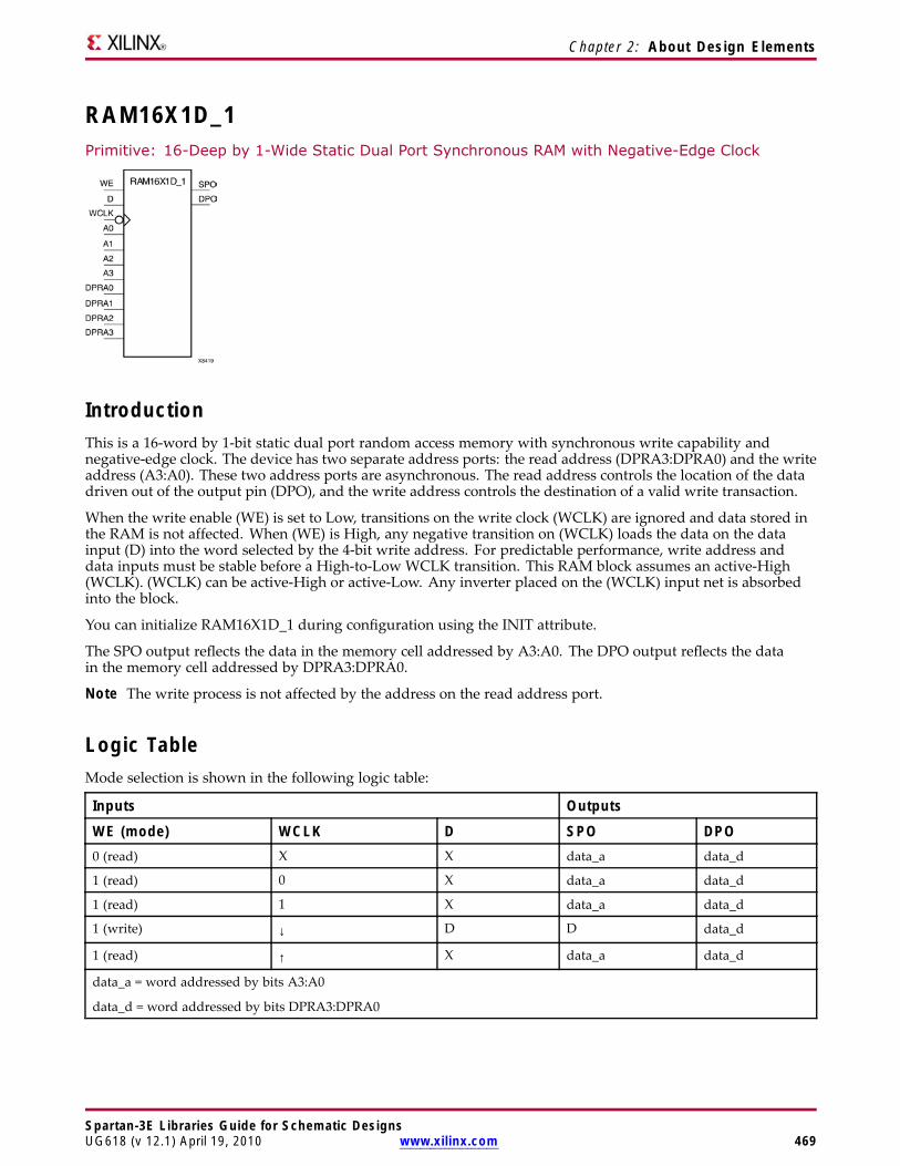
Chapter 2: About Design Elements
RAM16X1D_1Primitive: 16-Deep by 1-Wide Static Dual Port Synchronous RAM with Negative-Edge Clock
IntroductionThis is a 16-word by 1-bit static dual port random access memory with synchronous write capability andnegative-edge clock. The device has two separate address ports: the read address (DPRA3:DPRA0) and the writeaddress (A3:A0). These two address ports are asynchronous. The read address controls the location of the datadriven out of the output pin (DPO), and the write address controls the destination of a valid write transaction.
When the write enable (WE) is set to Low, transitions on the write clock (WCLK) are ignored and data stored inthe RAM is not affected. When (WE) is High, any negative transition on (WCLK) loads the data on the datainput (D) into the word selected by the 4-bit write address. For predictable performance, write address anddata inputs must be stable before a High-to-Low WCLK transition. This RAM block assumes an active-High(WCLK). (WCLK) can be active-High or active-Low. Any inverter placed on the (WCLK) input net is absorbedinto the block.
You can initialize RAM16X1D_1 during configuration using the INIT attribute.
The SPO output reflects the data in the memory cell addressed by A3:A0. The DPO output reflects the datain the memory cell addressed by DPRA3:DPRA0.
Note The write process is not affected by the address on the read address port.
Logic TableMode selection is shown in the following logic table:
Inputs Outputs
WE (mode) WCLK D SPO DPO0 (read) X X data_a data_d
1 (read) 0 X data_a data_d
1 (read) 1 X data_a data_d
1 (write) ↓ D D data_d
1 (read) ↑ X data_a data_d
data_a = word addressed by bits A3:A0
data_d = word addressed by bits DPRA3:DPRA0
Spartan-3E Libraries Guide for Schematic DesignsUG618 (v 12.1) April 19, 2010 www.xilinx.com 469
Chapter 2: About Design Elements
Port DescriptionsPort Direction Width FunctionDPO Output 1 Read-only 1-Bit data output
SPO Output 1 R/W 1-Bit data output
A0 Input 1 R/W address[0] input
A1 Input 1 R/W address[1] input
A2 Input 1 R/W address[2] input
A3 Input 1 R/W address[3] input
D Input 1 Write 1-Bit data input
DPRA0 Input 1 Read-only address[0] input
DPRA1 Input 1 Read-only address[1] input
DPRA2 Input 1 Read-only address[2] input
DPRA3 Input 1 Read-only address[3] input
WCLK Input 1 Write clock input
WE Input 1 Write enable input
Design Entry MethodThis design element can be used in schematics.
Available Attributes
Attribute TypeAllowedValues Default Description
INIT Hexadecimal Any 16-Bit Value All zeros Initializes RAMs, registers, and look-uptables.
For More Information• See the Spartan-3 Generation FPGA User Guide.
• See the Spartan-3E FPGA Family Complete Data Sheet.
Spartan-3E Libraries Guide for Schematic Designs470 www.xilinx.com UG618 (v 12.1) April 19, 2010
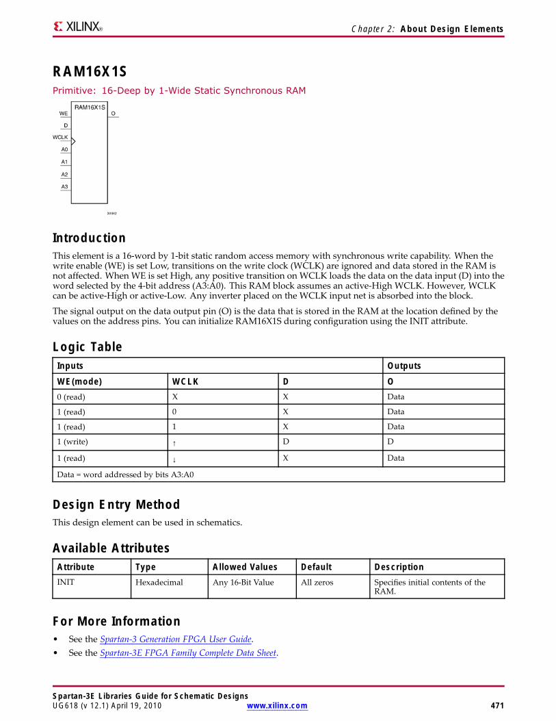
Chapter 2: About Design Elements
RAM16X1SPrimitive: 16-Deep by 1-Wide Static Synchronous RAM
IntroductionThis element is a 16-word by 1-bit static random access memory with synchronous write capability. When thewrite enable (WE) is set Low, transitions on the write clock (WCLK) are ignored and data stored in the RAM isnot affected. When WE is set High, any positive transition on WCLK loads the data on the data input (D) into theword selected by the 4-bit address (A3:A0). This RAM block assumes an active-High WCLK. However, WCLKcan be active-High or active-Low. Any inverter placed on the WCLK input net is absorbed into the block.
The signal output on the data output pin (O) is the data that is stored in the RAM at the location defined by thevalues on the address pins. You can initialize RAM16X1S during configuration using the INIT attribute.
Logic TableInputs Outputs
WE(mode) WCLK D O0 (read) X X Data
1 (read) 0 X Data
1 (read) 1 X Data
1 (write) ↑ D D
1 (read) ↓ X Data
Data = word addressed by bits A3:A0
Design Entry MethodThis design element can be used in schematics.
Available AttributesAttribute Type Allowed Values Default DescriptionINIT Hexadecimal Any 16-Bit Value All zeros Specifies initial contents of the
RAM.
For More Information• See the Spartan-3 Generation FPGA User Guide.• See the Spartan-3E FPGA Family Complete Data Sheet.
Spartan-3E Libraries Guide for Schematic DesignsUG618 (v 12.1) April 19, 2010 www.xilinx.com 471
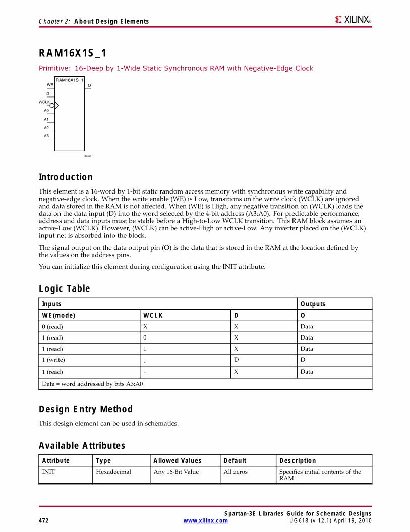
Chapter 2: About Design Elements
RAM16X1S_1Primitive: 16-Deep by 1-Wide Static Synchronous RAM with Negative-Edge Clock
IntroductionThis element is a 16-word by 1-bit static random access memory with synchronous write capability andnegative-edge clock. When the write enable (WE) is Low, transitions on the write clock (WCLK) are ignoredand data stored in the RAM is not affected. When (WE) is High, any negative transition on (WCLK) loads thedata on the data input (D) into the word selected by the 4-bit address (A3:A0). For predictable performance,address and data inputs must be stable before a High-to-Low WCLK transition. This RAM block assumes anactive-Low (WCLK). However, (WCLK) can be active-High or active-Low. Any inverter placed on the (WCLK)input net is absorbed into the block.
The signal output on the data output pin (O) is the data that is stored in the RAM at the location defined bythe values on the address pins.
You can initialize this element during configuration using the INIT attribute.
Logic TableInputs Outputs
WE(mode) WCLK D O0 (read) X X Data
1 (read) 0 X Data
1 (read) 1 X Data
1 (write) ↓ D D
1 (read) ↑ X Data
Data = word addressed by bits A3:A0
Design Entry MethodThis design element can be used in schematics.
Available AttributesAttribute Type Allowed Values Default DescriptionINIT Hexadecimal Any 16-Bit Value All zeros Specifies initial contents of the
RAM.
Spartan-3E Libraries Guide for Schematic Designs472 www.xilinx.com UG618 (v 12.1) April 19, 2010

Chapter 2: About Design Elements
For More Information• See the Spartan-3 Generation FPGA User Guide.
• See the Spartan-3E FPGA Family Complete Data Sheet.
Spartan-3E Libraries Guide for Schematic DesignsUG618 (v 12.1) April 19, 2010 www.xilinx.com 473
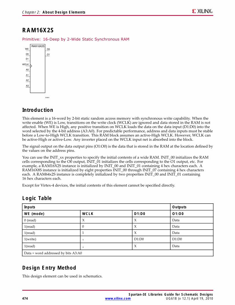
Chapter 2: About Design Elements
RAM16X2SPrimitive: 16-Deep by 2-Wide Static Synchronous RAM
IntroductionThis element is a 16-word by 2-bit static random access memory with synchronous write capability. When thewrite enable (WE) is Low, transitions on the write clock (WCLK) are ignored and data stored in the RAM is notaffected. When WE is High, any positive transition on WCLK loads the data on the data input (D1:D0) into theword selected by the 4-bit address (A3:A0). For predictable performance, address and data inputs must be stablebefore a Low-to-High WCLK transition. This RAM block assumes an active-High WCLK. However, WCLK canbe active-High or active-Low. Any inverter placed on the WCLK input net is absorbed into the block.
The signal output on the data output pins (O1:O0) is the data that is stored in the RAM at the location defined bythe values on the address pins.
You can use the INIT_xx properties to specify the initial contents of a wide RAM. INIT_00 initializes the RAMcells corresponding to the O0 output, INIT_01 initializes the cells corresponding to the O1 output, etc. Forexample, a RAM16X2S instance is initialized by INIT_00 and INIT_01 containing 4 hex characters each. ARAM16X8S instance is initialized by eight properties INIT_00 through INIT_07 containing 4 hex characterseach. A RAM64x2S instance is completely initialized by two properties INIT_00 and INIT_01 containing16 hex characters each.
Except for Virtex-4 devices, the initial contents of this element cannot be specified directly.
Logic TableInputs Outputs
WE (mode) WCLK D1:D0 O1:O00 (read) X X Data
1(read) 0 X Data
1(read) 1 X Data
1(write) ↑ D1:D0 D1:D0
1(read) ↓ X Data
Data = word addressed by bits A3:A0
Design Entry MethodThis design element can be used in schematics.
Spartan-3E Libraries Guide for Schematic Designs474 www.xilinx.com UG618 (v 12.1) April 19, 2010

Chapter 2: About Design Elements
Available AttributesAttribute Type Allowed Values Default DescriptionINIT_00 to INIT_01 Hexadecimal Any 16-Bit Value All zeros Initializes RAMs, registers, and
look-up tables.
For More Information• See the Spartan-3 Generation FPGA User Guide.
• See the Spartan-3E FPGA Family Complete Data Sheet.
Spartan-3E Libraries Guide for Schematic DesignsUG618 (v 12.1) April 19, 2010 www.xilinx.com 475
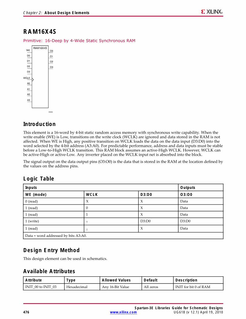
Chapter 2: About Design Elements
RAM16X4SPrimitive: 16-Deep by 4-Wide Static Synchronous RAM
IntroductionThis element is a 16-word by 4-bit static random access memory with synchronous write capability. When thewrite enable (WE) is Low, transitions on the write clock (WCLK) are ignored and data stored in the RAM is notaffected. When WE is High, any positive transition on WCLK loads the data on the data input (D3:D0) into theword selected by the 4-bit address (A3:A0). For predictable performance, address and data inputs must be stablebefore a Low-to-High WCLK transition. This RAM block assumes an active-High WCLK. However, WCLK canbe active-High or active-Low. Any inverter placed on the WCLK input net is absorbed into the block.
The signal output on the data output pins (O3:O0) is the data that is stored in the RAM at the location defined bythe values on the address pins.
Logic TableInputs Outputs
WE (mode) WCLK D3:D0 O3:O00 (read) X X Data
1 (read) 0 X Data
1 (read) 1 X Data
1 (write) ↑ D3:D0 D3:D0
1 (read) ↓ X Data
Data = word addressed by bits A3:A0.
Design Entry MethodThis design element can be used in schematics.
Available AttributesAttribute Type Allowed Values Default DescriptionINIT_00 to INIT_03 Hexadecimal Any 16-Bit Value All zeros INIT for bit 0 of RAM
Spartan-3E Libraries Guide for Schematic Designs476 www.xilinx.com UG618 (v 12.1) April 19, 2010

Chapter 2: About Design Elements
For More Information• See the Spartan-3 Generation FPGA User Guide.
• See the Spartan-3E FPGA Family Complete Data Sheet.
Spartan-3E Libraries Guide for Schematic DesignsUG618 (v 12.1) April 19, 2010 www.xilinx.com 477
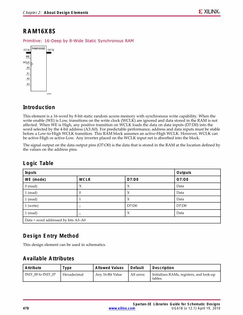
Chapter 2: About Design Elements
RAM16X8SPrimitive: 16-Deep by 8-Wide Static Synchronous RAM
IntroductionThis element is a 16-word by 8-bit static random access memory with synchronous write capability. When thewrite enable (WE) is Low, transitions on the write clock (WCLK) are ignored and data stored in the RAM is notaffected. When WE is High, any positive transition on WCLK loads the data on data inputs (D7:D0) into theword selected by the 4-bit address (A3:A0). For predictable performance, address and data inputs must be stablebefore a Low-to-High WCLK transition. This RAM block assumes an active-High WCLK. However, WCLK canbe active-High or active-Low. Any inverter placed on the WCLK input net is absorbed into the block.
The signal output on the data output pins (O7:O0) is the data that is stored in the RAM at the location defined bythe values on the address pins.
Logic TableInputs Outputs
WE (mode) WCLK D7:D0 O7:O00 (read) X X Data
1 (read) 0 X Data
1 (read) 1 X Data
1 (write) ↑ D7:D0 D7:D0
1 (read) ↓ X Data
Data = word addressed by bits A3–A0
Design Entry MethodThis design element can be used in schematics.
Available AttributesAttribute Type Allowed Values Default DescriptionINIT_00 to INIT_07 Hexadecimal Any 16-Bit Value All zeros Initializes RAMs, registers, and look-up
tables.
Spartan-3E Libraries Guide for Schematic Designs478 www.xilinx.com UG618 (v 12.1) April 19, 2010

Chapter 2: About Design Elements
For More Information• See the Spartan-3 Generation FPGA User Guide.
• See the Spartan-3E FPGA Family Complete Data Sheet.
Spartan-3E Libraries Guide for Schematic DesignsUG618 (v 12.1) April 19, 2010 www.xilinx.com 479
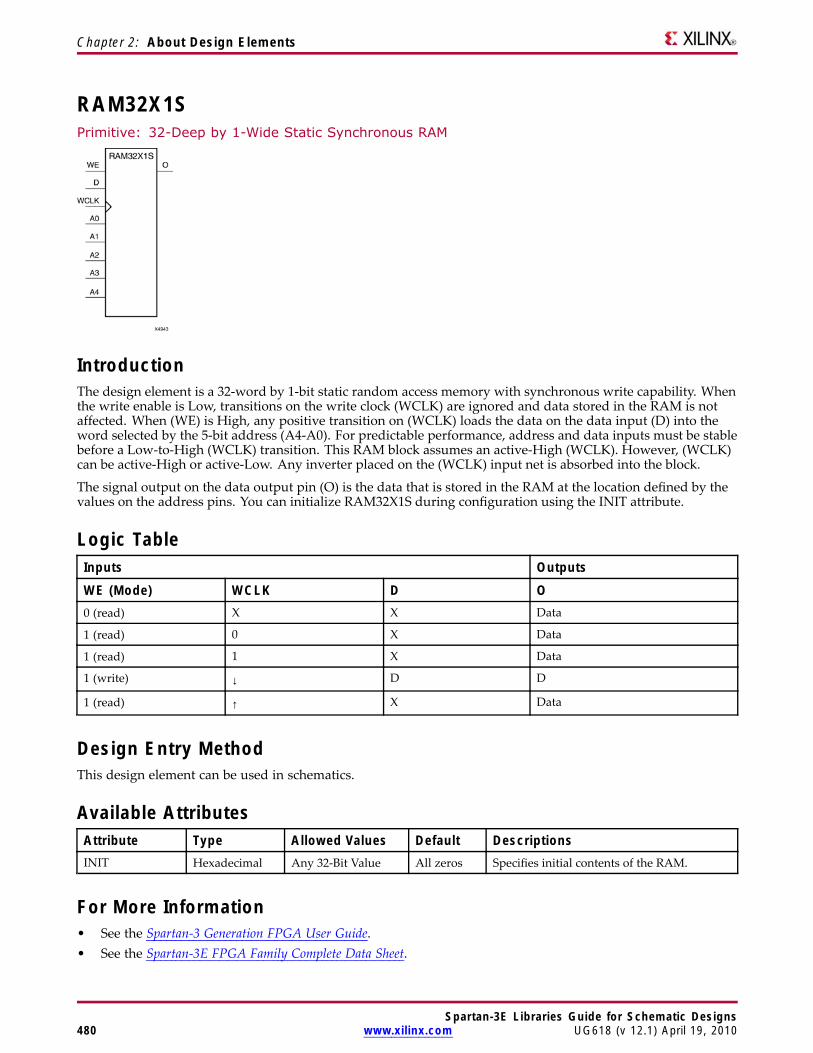
Chapter 2: About Design Elements
RAM32X1SPrimitive: 32-Deep by 1-Wide Static Synchronous RAM
IntroductionThe design element is a 32-word by 1-bit static random access memory with synchronous write capability. Whenthe write enable is Low, transitions on the write clock (WCLK) are ignored and data stored in the RAM is notaffected. When (WE) is High, any positive transition on (WCLK) loads the data on the data input (D) into theword selected by the 5-bit address (A4-A0). For predictable performance, address and data inputs must be stablebefore a Low-to-High (WCLK) transition. This RAM block assumes an active-High (WCLK). However, (WCLK)can be active-High or active-Low. Any inverter placed on the (WCLK) input net is absorbed into the block.
The signal output on the data output pin (O) is the data that is stored in the RAM at the location defined by thevalues on the address pins. You can initialize RAM32X1S during configuration using the INIT attribute.
Logic TableInputs Outputs
WE (Mode) WCLK D O0 (read) X X Data
1 (read) 0 X Data
1 (read) 1 X Data
1 (write) ↓ D D
1 (read) ↑ X Data
Design Entry MethodThis design element can be used in schematics.
Available AttributesAttribute Type Allowed Values Default DescriptionsINIT Hexadecimal Any 32-Bit Value All zeros Specifies initial contents of the RAM.
For More Information• See the Spartan-3 Generation FPGA User Guide.• See the Spartan-3E FPGA Family Complete Data Sheet.
Spartan-3E Libraries Guide for Schematic Designs480 www.xilinx.com UG618 (v 12.1) April 19, 2010
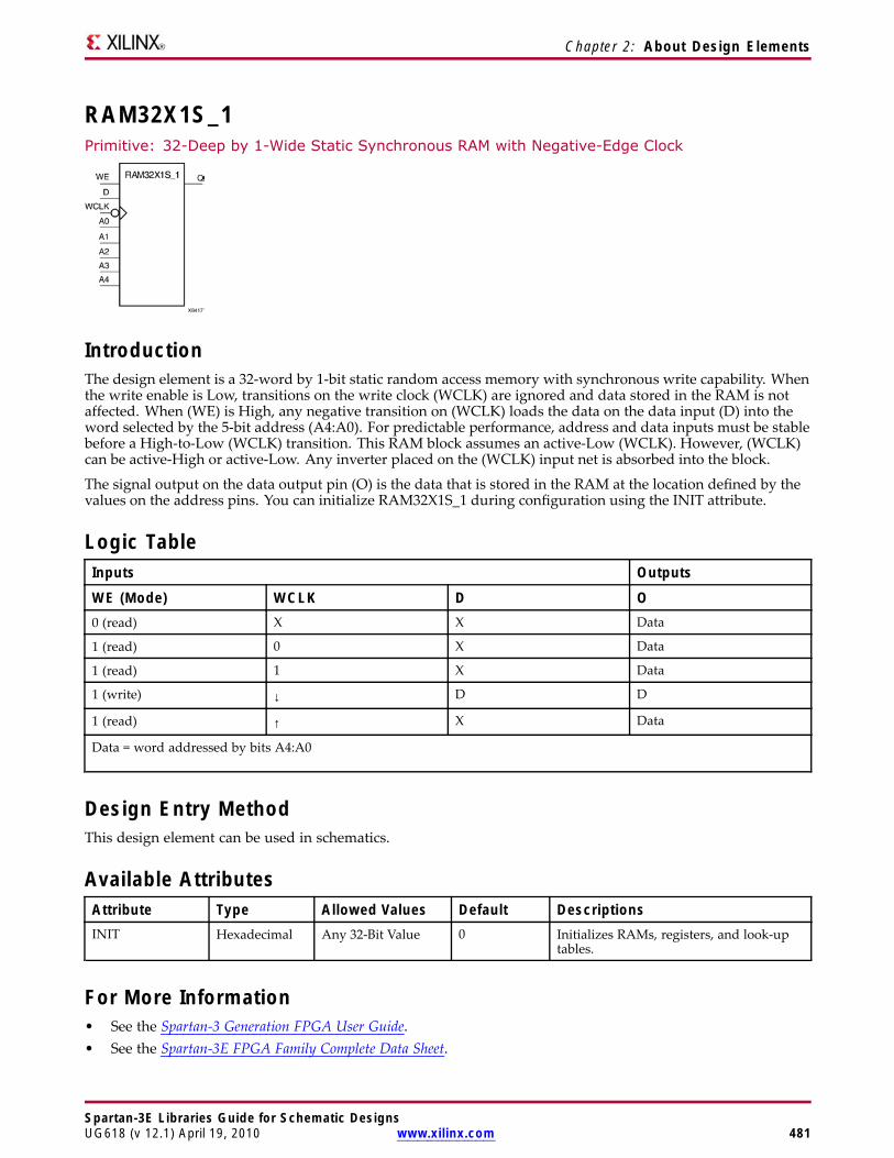
Chapter 2: About Design Elements
RAM32X1S_1Primitive: 32-Deep by 1-Wide Static Synchronous RAM with Negative-Edge Clock
IntroductionThe design element is a 32-word by 1-bit static random access memory with synchronous write capability. Whenthe write enable is Low, transitions on the write clock (WCLK) are ignored and data stored in the RAM is notaffected. When (WE) is High, any negative transition on (WCLK) loads the data on the data input (D) into theword selected by the 5-bit address (A4:A0). For predictable performance, address and data inputs must be stablebefore a High-to-Low (WCLK) transition. This RAM block assumes an active-Low (WCLK). However, (WCLK)can be active-High or active-Low. Any inverter placed on the (WCLK) input net is absorbed into the block.
The signal output on the data output pin (O) is the data that is stored in the RAM at the location defined by thevalues on the address pins. You can initialize RAM32X1S_1 during configuration using the INIT attribute.
Logic TableInputs Outputs
WE (Mode) WCLK D O0 (read) X X Data
1 (read) 0 X Data
1 (read) 1 X Data
1 (write) ↓ D D
1 (read) ↑ X Data
Data = word addressed by bits A4:A0
Design Entry MethodThis design element can be used in schematics.
Available AttributesAttribute Type Allowed Values Default DescriptionsINIT Hexadecimal Any 32-Bit Value 0 Initializes RAMs, registers, and look-up
tables.
For More Information• See the Spartan-3 Generation FPGA User Guide.• See the Spartan-3E FPGA Family Complete Data Sheet.
Spartan-3E Libraries Guide for Schematic DesignsUG618 (v 12.1) April 19, 2010 www.xilinx.com 481
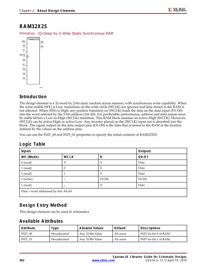
Chapter 2: About Design Elements
RAM32X2SPrimitive: 32-Deep by 2-Wide Static Synchronous RAM
IntroductionThe design element is a 32-word by 2-bit static random access memory with synchronous write capability. Whenthe write enable (WE) is Low, transitions on the write clock (WCLK) are ignored and data stored in the RAM isnot affected. When (WE) is High, any positive transition on (WCLK) loads the data on the data input (D1-D0)into the word selected by the 5-bit address (A4-A0). For predictable performance, address and data inputs mustbe stable before a Low-to-High (WCLK) transition. This RAM block assumes an active-High (WCLK). However,(WCLK) can be active-High or active-Low. Any inverter placed on the (WCLK) input net is absorbed into theblock. The signal output on the data output pins (O1-O0) is the data that is stored in the RAM at the locationdefined by the values on the address pins.
You can use the INIT_00 and INIT_01 properties to specify the initial contents of RAM32X2S.
Logic TableInputs Outputs
WE (Mode) WCLK D O0-O10 (read) X X Data
1 (read) 0 X Data
1 (read) 1 X Data
1 (write) ↑ D1:D0 D1:D0
1 (read) ↓ X Data
Data = word addressed by bits A4:A0
Design Entry MethodThis design element can be used in schematics.
Available AttributesAttribute Type Allowed Values Default DescriptionsINIT_00 Hexadecimal Any 32-Bit Value All zeros INIT for bit 0 of RAM.
INIT_01 Hexadecimal Any 32-Bit Value All zeros INIT for bit 1 of RAM.
Spartan-3E Libraries Guide for Schematic Designs482 www.xilinx.com UG618 (v 12.1) April 19, 2010

Chapter 2: About Design Elements
For More Information• See the Spartan-3 Generation FPGA User Guide.
• See the Spartan-3E FPGA Family Complete Data Sheet.
Spartan-3E Libraries Guide for Schematic DesignsUG618 (v 12.1) April 19, 2010 www.xilinx.com 483
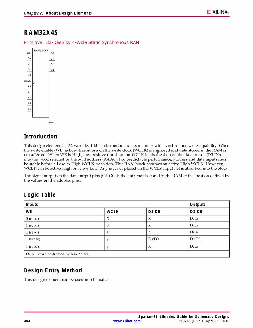
Chapter 2: About Design Elements
RAM32X4SPrimitive: 32-Deep by 4-Wide Static Synchronous RAM
IntroductionThis design element is a 32-word by 4-bit static random access memory with synchronous write capability. Whenthe write enable (WE) is Low, transitions on the write clock (WCLK) are ignored and data stored in the RAM isnot affected. When WE is High, any positive transition on WCLK loads the data on the data inputs (D3-D0)into the word selected by the 5-bit address (A4:A0). For predictable performance, address and data inputs mustbe stable before a Low-to-High WCLK transition. This RAM block assumes an active-High WCLK. However,WCLK can be active-High or active-Low. Any inverter placed on the WCLK input net is absorbed into the block.
The signal output on the data output pins (O3-O0) is the data that is stored in the RAM at the location defined bythe values on the address pins.
Logic TableInputs Outputs
WE WCLK D3-D0 O3-O00 (read) X X Data
1 (read) 0 X Data
1 (read) 1 X Data
1 (write) ↑ D3:D0 D3:D0
1 (read) ↓ X Data
Data = word addressed by bits A4:A0
Design Entry MethodThis design element can be used in schematics.
Spartan-3E Libraries Guide for Schematic Designs484 www.xilinx.com UG618 (v 12.1) April 19, 2010
Chapter 2: About Design Elements
Available AttributesAttribute Type Allowed Values Default DescriptionINIT_00 Hexadecimal Any 32-Bit Value All zeros INIT for bit 0 of RAM.
INIT_01 Hexadecimal Any 32-Bit Value All zeros INIT for bit 1 of RAM.
INIT_02 Hexadecimal Any 32-Bit Value All zeros INIT for bit 2 of RAM.
INIT_03 Hexadecimal Any 32-Bit Value All zeros INIT for bit 3 of RAM.
For More Information• See the Spartan-3 Generation FPGA User Guide.
• See the Spartan-3E FPGA Family Complete Data Sheet.
Spartan-3E Libraries Guide for Schematic DesignsUG618 (v 12.1) April 19, 2010 www.xilinx.com 485
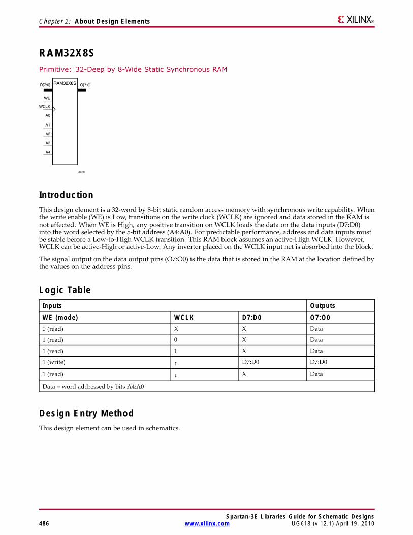
Chapter 2: About Design Elements
RAM32X8SPrimitive: 32-Deep by 8-Wide Static Synchronous RAM
IntroductionThis design element is a 32-word by 8-bit static random access memory with synchronous write capability. Whenthe write enable (WE) is Low, transitions on the write clock (WCLK) are ignored and data stored in the RAM isnot affected. When WE is High, any positive transition on WCLK loads the data on the data inputs (D7:D0)into the word selected by the 5-bit address (A4:A0). For predictable performance, address and data inputs mustbe stable before a Low-to-High WCLK transition. This RAM block assumes an active-High WCLK. However,WCLK can be active-High or active-Low. Any inverter placed on the WCLK input net is absorbed into the block.
The signal output on the data output pins (O7:O0) is the data that is stored in the RAM at the location defined bythe values on the address pins.
Logic TableInputs Outputs
WE (mode) WCLK D7:D0 O7:O00 (read) X X Data
1 (read) 0 X Data
1 (read) 1 X Data
1 (write) ↑ D7:D0 D7:D0
1 (read) ↓ X Data
Data = word addressed by bits A4:A0
Design Entry MethodThis design element can be used in schematics.
Spartan-3E Libraries Guide for Schematic Designs486 www.xilinx.com UG618 (v 12.1) April 19, 2010
Chapter 2: About Design Elements
Available AttributesAttribute Type Allowed Values Default DescriptionINIT_00 Hexadecimal Any 32-Bit Value All zeros INIT for bit 0 of RAM.
INIT_01 Hexadecimal Any 32-Bit Value All zeros INIT for bit 1 of RAM.
INIT_02 Hexadecimal Any 32-Bit Value All zeros INIT for bit 2 of RAM.
INIT_03 Hexadecimal Any 32-Bit Value All zeros INIT for bit 3 of RAM.
INIT_04 Hexadecimal Any 32-Bit Value All zeros INIT for bit 4 of RAM.
INIT_05 Hexadecimal Any 32-Bit Value All zeros INIT for bit 5 of RAM.
INIT_06 Hexadecimal Any 32-Bit Value All zeros INIT for bit 6 of RAM.
INIT_07 Hexadecimal Any 32-Bit Value All zeros INIT for bit 7 of RAM.
For More Information• See the Spartan-3 Generation FPGA User Guide.
• See the Spartan-3E FPGA Family Complete Data Sheet.
Spartan-3E Libraries Guide for Schematic DesignsUG618 (v 12.1) April 19, 2010 www.xilinx.com 487
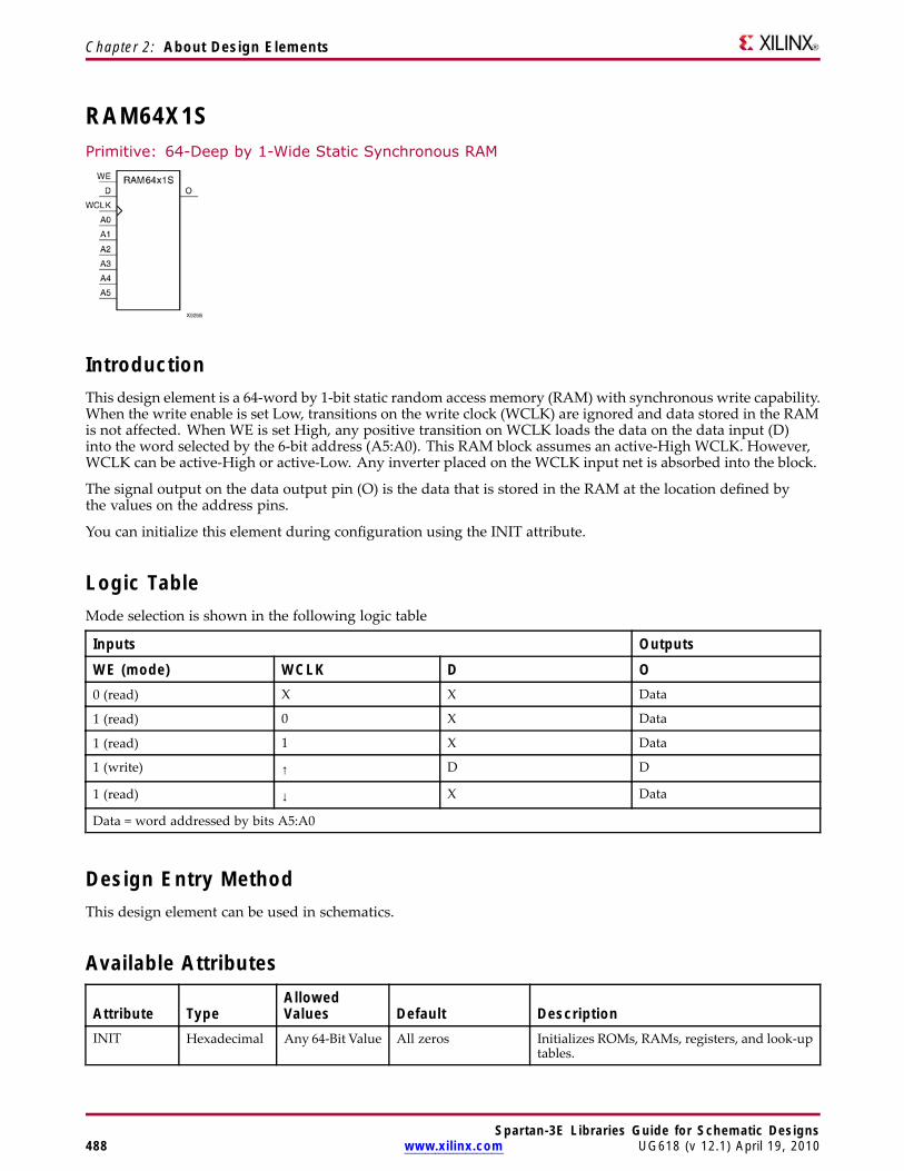
Chapter 2: About Design Elements
RAM64X1SPrimitive: 64-Deep by 1-Wide Static Synchronous RAM
IntroductionThis design element is a 64-word by 1-bit static random access memory (RAM) with synchronous write capability.When the write enable is set Low, transitions on the write clock (WCLK) are ignored and data stored in the RAMis not affected. When WE is set High, any positive transition on WCLK loads the data on the data input (D)into the word selected by the 6-bit address (A5:A0). This RAM block assumes an active-High WCLK. However,WCLK can be active-High or active-Low. Any inverter placed on the WCLK input net is absorbed into the block.
The signal output on the data output pin (O) is the data that is stored in the RAM at the location defined bythe values on the address pins.
You can initialize this element during configuration using the INIT attribute.
Logic TableMode selection is shown in the following logic table
Inputs Outputs
WE (mode) WCLK D O0 (read) X X Data
1 (read) 0 X Data
1 (read) 1 X Data
1 (write) ↑ D D
1 (read) ↓ X Data
Data = word addressed by bits A5:A0
Design Entry MethodThis design element can be used in schematics.
Available Attributes
Attribute TypeAllowedValues Default Description
INIT Hexadecimal Any 64-Bit Value All zeros Initializes ROMs, RAMs, registers, and look-uptables.
Spartan-3E Libraries Guide for Schematic Designs488 www.xilinx.com UG618 (v 12.1) April 19, 2010

Chapter 2: About Design Elements
For More Information• See the Spartan-3 Generation FPGA User Guide.
• See the Spartan-3E FPGA Family Complete Data Sheet.
Spartan-3E Libraries Guide for Schematic DesignsUG618 (v 12.1) April 19, 2010 www.xilinx.com 489
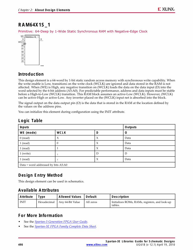
Chapter 2: About Design Elements
RAM64X1S_1Primitive: 64-Deep by 1-Wide Static Synchronous RAM with Negative-Edge Clock
IntroductionThis design element is a 64-word by 1-bit static random access memory with synchronous write capability. Whenthe write enable is Low, transitions on the write clock (WCLK) are ignored and data stored in the RAM is notaffected. When (WE) is High, any negative transition on (WCLK) loads the data on the data input (D) into theword selected by the 6-bit address (A5:A0). For predictable performance, address and data inputs must be stablebefore a High-to-Low (WCLK) transition. This RAM block assumes an active-Low (WCLK). However, (WCLK)can be active-High or active-Low. Any inverter placed on the (WCLK) input net is absorbed into the block.
The signal output on the data output pin (O) is the data that is stored in the RAM at the location defined bythe values on the address pins.
You can initialize this element during configuration using the INIT attribute.
Logic TableInputs Outputs
WE (mode) WCLK D O0 (read) X X Data
1 (read) 0 X Data
1 (read) 1 X Data
1 (write) ↓ D D
1 (read) ↑ X Data
Data = word addressed by bits A5:A0
Design Entry MethodThis design element can be used in schematics.
Available AttributesAttribute Type Allowed Values Default DescriptionINIT Hexadecimal Any 64-Bit Value All zeros Initializes ROMs, RAMs, registers, and look-up
tables.
For More Information• See the Spartan-3 Generation FPGA User Guide.• See the Spartan-3E FPGA Family Complete Data Sheet.
Spartan-3E Libraries Guide for Schematic Designs490 www.xilinx.com UG618 (v 12.1) April 19, 2010
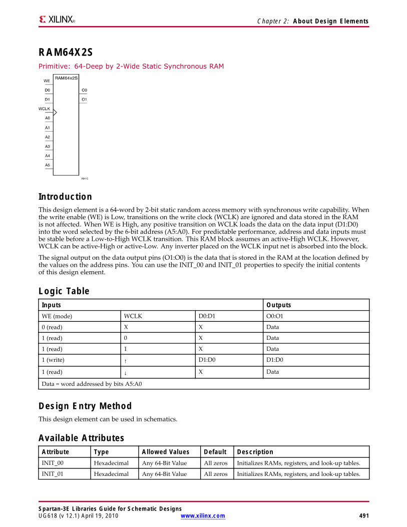
Chapter 2: About Design Elements
RAM64X2SPrimitive: 64-Deep by 2-Wide Static Synchronous RAM
IntroductionThis design element is a 64-word by 2-bit static random access memory with synchronous write capability. Whenthe write enable (WE) is Low, transitions on the write clock (WCLK) are ignored and data stored in the RAMis not affected. When WE is High, any positive transition on WCLK loads the data on the data input (D1:D0)into the word selected by the 6-bit address (A5:A0). For predictable performance, address and data inputs mustbe stable before a Low-to-High WCLK transition. This RAM block assumes an active-High WCLK. However,WCLK can be active-High or active-Low. Any inverter placed on the WCLK input net is absorbed into the block.
The signal output on the data output pins (O1:O0) is the data that is stored in the RAM at the location defined bythe values on the address pins. You can use the INIT_00 and INIT_01 properties to specify the initial contentsof this design element.
Logic TableInputs OutputsWE (mode) WCLK D0:D1 O0:O1
0 (read) X X Data
1 (read) 0 X Data
1 (read) 1 X Data
1 (write) ↑ D1:D0 D1:D0
1 (read) ↓ X Data
Data = word addressed by bits A5:A0
Design Entry MethodThis design element can be used in schematics.
Available AttributesAttribute Type Allowed Values Default DescriptionINIT_00 Hexadecimal Any 64-Bit Value All zeros Initializes RAMs, registers, and look-up tables.
INIT_01 Hexadecimal Any 64-Bit Value All zeros Initializes RAMs, registers, and look-up tables.
Spartan-3E Libraries Guide for Schematic DesignsUG618 (v 12.1) April 19, 2010 www.xilinx.com 491

Chapter 2: About Design Elements
For More Information• See the Spartan-3 Generation FPGA User Guide.
• See the Spartan-3E FPGA Family Complete Data Sheet.
Spartan-3E Libraries Guide for Schematic Designs492 www.xilinx.com UG618 (v 12.1) April 19, 2010
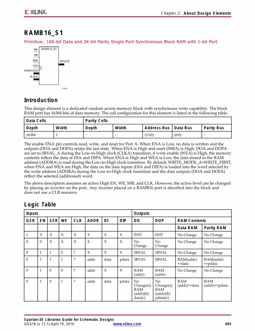
Chapter 2: About Design Elements
RAMB16_S1Primitive: 16K-bit Data and 2K-bit Parity Single-Port Synchronous Block RAM with 1-bit Port
IntroductionThis design element is a dedicated random access memory block with synchronous write capability. The blockRAM port has 16384 bits of data memory. The cell configuration for this element is listed in the following table.
Data Cells Parity CellsDepth Width Depth Width Address Bus Data Bus Parity Bus16384 1 - - (13:0) (0:0) -
The enable ENA pin controls read, write, and reset for Port A. When ENA is Low, no data is written and theoutputs (DOA and DOPA) retain the last state. When ENA is High and reset (SSRA) is High, DOA and DOPAare set to SRVAL_A during the Low-to-High clock (CLKA) transition; if write enable (WEA) is High, the memorycontents reflect the data at DIA and DIPA. When ENA is High and WEA is Low, the data stored in the RAMaddress (ADDRA) is read during the Low-to-High clock transition. By default, WRITE_MODE_A=WRITE_FIRST,when ENA and WEA are High, the data on the data inputs (DIA and DIPA) is loaded into the word selected bythe write address (ADDRA) during the Low-to-High clock transition and the data outputs (DOA and DOPA)reflect the selected (addressed) word.
The above description assumes an active High EN, WE, SSR, and CLK. However, the active level can be changedby placing an inverter on the port. Any inverter placed on a RAMB16 port is absorbed into the block anddoes not use a CLB resource.
Logic TableInputs Outputs
GSR EN SSR WE CLK ADDR DI DIP DO DOP RAM ContentsData RAM Parity RAM
1 X X X X X X X INIT INIT No Change No Change
0 0 X X X X X X NoChange
NoChange
No Change No Change
0 1 1 0 ? X X X SRVAL SRVAL No Change No Change
0 1 1 1 ? addr data pdata SRVAL SRVAL RAM(addr)=>data
RAM(addr)=>pdata
0 1 0 0 ? addr X X RAM(addr)
RAM(addr)
No Change No Change
0 1 0 1 ? addr data pdata NoChange(a)RAM(addr)(b)data(c)
NoChange(a)RAM(addr)(b)pdata(c)
RAM(addr)=>data
RAM(addr)=>pdata
Spartan-3E Libraries Guide for Schematic DesignsUG618 (v 12.1) April 19, 2010 www.xilinx.com 493
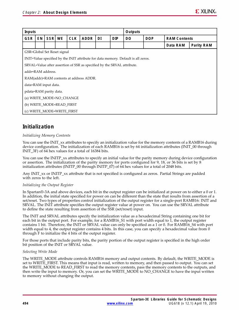
Chapter 2: About Design Elements
Inputs Outputs
GSR EN SSR WE CLK ADDR DI DIP DO DOP RAM ContentsData RAM Parity RAM
GSR=Global Set Reset signal
INIT=Value specified by the INIT attribute for data memory. Default is all zeros.
SRVAL=Value after assertion of SSR as specified by the SRVAL attribute.
addr=RAM address.
RAM(addr)=RAM contents at address ADDR.
data=RAM input data.
pdata=RAM parity data.
(a) WRITE_MODE=NO_CHANGE
(b) WRITE_MODE=READ_FIRST
(c) WRITE_MODE=WRITE_FIRST
InitializationInitializing Memory Contents
You can use the INIT_xx attributes to specify an initialization value for the memory contents of a RAMB16 duringdevice configuration. The initialization of each RAMB16 is set by 64 initialization attributes (INIT_00 throughINIT_3F) of 64 hex values for a total of 16384 bits.
You can use the INITP_xx attributes to specify an initial value for the parity memory during device configurationor assertion. The initialization of the parity memory for ports configured for 9, 18, or 36 bits is set by 8initialization attributes (INITP_00 through INITP_07) of 64 hex values for a total of 2048 bits.
Any INIT_xx or INITP_xx attribute that is not specified is configured as zeros. Partial Strings are paddedwith zeros to the left.
Initializing the Output Register
In Spartan®-3A and above devices, each bit in the output register can be initialized at power on to either a 0 or 1.In addition, the initial state specified for power on can be different than the state that results from assertion of aset/reset. Two types of properties control initialization of the output register for a single-port RAMB16: INIT andSRVAL. The INIT attribute specifies the output register value at power on. You can use the SRVAL attributeto define the state resulting from assertion of the SSR (set/reset) input.
The INIT and SRVAL attributes specify the initialization value as a hexadecimal String containing one bit foreach bit in the output port. For example, for a RAMB16_S1 with port width equal to 1, the output registercontains 1 bit. Therefore, the INIT or SRVAL value can only be specified as a 1 or 0. For RAMB16_S4 with portwidth equal to 4, the output register contains 4 bits. In this case, you can specify a hexadecimal value from 0through F to initialize the 4 bits of the output register.
For those ports that include parity bits, the parity portion of the output register is specified in the high orderbit position of the INIT or SRVAL value.
Selecting Write Mode
The WRITE_MODE attribute controls RAMB16 memory and output contents. By default, the WRITE_MODE isset to WRITE_FIRST. This means that input is read, written to memory, and then passed to output. You can setthe WRITE_MODE to READ_FIRST to read the memory contents, pass the memory contents to the outputs, andthen write the input to memory. Or, you can set the WRITE_MODE to NO_CHANGE to have the input writtento memory without changing the output.
Spartan-3E Libraries Guide for Schematic Designs494 www.xilinx.com UG618 (v 12.1) April 19, 2010

Chapter 2: About Design Elements
Design Entry MethodThis design element can be used in schematics.
Available Attributes
Attribute TypeAllowedValues Default Description
INIT Binary/Hexadecimal
Any Hex Value All zeros Identifies the initial value of theDO output port after completingconfiguration. The bit width is dependenton the width of the A or B port of theRAM.
INIT_00 toINIT_3F
Binary/Hexadecimal
Any Hex Value All zeros Specifies the initial contents of the dataportion of the RAM array.
INITP_00 toINITP_07
Binary/Hexadecimal
Any Hex Value All zeros Specifies the initial contents of the parityportion of the RAM array.
SRVAL Binary/Hexadecimal
Any Hex Value All zeros Allows the individual selection ofwhether the DO output port sets (go toa one) or reset (go to a zero) upon theassertion of the SSR pin. The bit widthis dependent on the width of the A or Bport of the RAM.
WRITE_MODE String "WRITE_FIRST","READ_FIRST"or"NO_CHANGE"
"WRITE_FIRST" Specifies the behavior of the DO portupon a write command to the respectedport. If set to "WRITE_FIRST", thesame port that is written to displaysthe contents of the written data tothe outputs upon completion of theoperation. "READ_FIRST" displaysthe prior contents of the RAM to theoutput port prior to writing the newdata. "NO_CHANGE" keeps the previousvalue on the output port and wont updatethe output port upon a write command.This is the suggested mode if not usingthe read data from a particular port of theRAM.
For More Information• See the Spartan-3 Generation FPGA User Guide.
• See the Spartan-3E FPGA Family Complete Data Sheet.
Spartan-3E Libraries Guide for Schematic DesignsUG618 (v 12.1) April 19, 2010 www.xilinx.com 495

Spartan-3E Libraries Guide for Schematic Designs496 www.xilinx.com UG618 (v 12.1) April 19, 2010
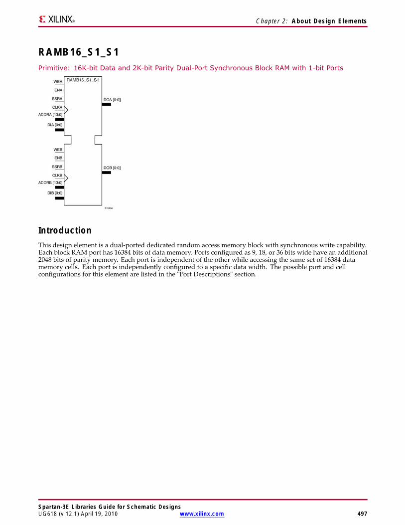
Chapter 2: About Design Elements
RAMB16_S1_S1Primitive: 16K-bit Data and 2K-bit Parity Dual-Port Synchronous Block RAM with 1-bit Ports
IntroductionThis design element is a dual-ported dedicated random access memory block with synchronous write capability.Each block RAM port has 16384 bits of data memory. Ports configured as 9, 18, or 36 bits wide have an additional2048 bits of parity memory. Each port is independent of the other while accessing the same set of 16384 datamemory cells. Each port is independently configured to a specific data width. The possible port and cellconfigurations for this element are listed in the "Port Descriptions" section.
Spartan-3E Libraries Guide for Schematic DesignsUG618 (v 12.1) April 19, 2010 www.xilinx.com 497

Chapter 2: About Design Elements
Logic TableTruth Table A
Inputs Outputs
GSR ENA SSRA WEA CLKA ADDRA DIA DIPA DOA DOPA RAM ContentsData RAM Parity RAM
1 X X X X X X X INIT_A INIT_A No Change No Change
0 0 X X X X X X No Change No Change No Change No Change
0 1 1 0 ? X X X SRVAL_A SRVAL_A No Change No Change
0 1 1 1 ? addr data pdata SRVAL_A SRVAL_A RAM(addr)=>data
RAM(addr)=>pdata
0 1 0 0 ? addr X X RAM(addr) RAM(addr) No Change No Change
0 1 0 1 ? addr data pdata No Change1,RAM(addr)2,data3
No Change1,RAM(addr)2,pdata3
RAM(addr)=>data
RAM(addr)=>pdata
GSR=Global Set Reset.
INIT_A=Value specified by the INIT_A attribute for output register. Default is all zeros.
SRVAL_A=register value.
addr=RAM address.
RAM(addr)=RAM contents at address ADDR.
data=RAM input data.
pdata=RAM parity data.
1WRITE_MODE_A=NO_CHANGE.
2WRITE_MODE_A=READ_FIRST.
3WRITE_MODE_A=WRITE_FIRST.
Spartan-3E Libraries Guide for Schematic Designs498 www.xilinx.com UG618 (v 12.1) April 19, 2010

Chapter 2: About Design Elements
Truth Table B
Inputs Outputs
GSR ENB SSRB WEB CLKB ADDRB DIB DIPB DOB DOPB RAM ContentsDataRAM
ParityRAM
1 X X X X X X X INIT_B INIT_B No Change No Change
0 0 X X X X X X No Change No Change No Change No Change
0 1 1 0 ? X X X SRVAL_B SRVAL_B No Change No Change
0 1 1 1 ? addr data pdata SRVAL_B SRVAL_B RAM(addr)=>data
RAM(addr)=>pdata
0 1 0 0 ? addr X X RAM(addr) RAM(addr) No Change No Change
0 1 0 1 ? addr data pdata No Change1,RAM(addr)=>data,data3
No Change1,RAM(addr)=>data,pdata3
RAM(addr)=>data
RAM(addr)=>pdata
GSR=Global Set Reset.
INIT_B=Value specified by the INIT_B attribute for output registers. Default is all zeros.
SRVAL_B=register value.
addr=RAM address.
RAM(addr)=RAM contents at address ADDR.
data=RAM input data.
pdata=RAM parity data.
1WRITE_MODE_B=NO_CHANGE.
2WRITE_MODE_B=READ_FIRST.
3WRITE_MODE_B=WRITE_FIRST.
Port DescriptionsPort A Port BDesignElement
DataCells(a)
ParityCells(a)
AddressBus
DataBus
ParityBus
DataCells(a)
ParityCells(a)
AddressBus
DataBus
ParityBus
RAMB16_S1_S1 16384 x1
- (13:0) (0:0) - 16384 x 1 - (13:0) (0:0) -
(a) Depth x Width
Each port is fully synchronous with independent clock pins. All Port A input pins have setup time referencedto the CLKA pin and its data output bus DOA has a clock-to-out time referenced to the CLKA. All Port Binput pins have setup time referenced to the CLKB pin and its data output bus DOB has a clock-to-out timereferenced to the CLKB. The enable ENA pin controls read, write, and reset for Port A. When ENA is Low, nodata is written and the outputs (DOA and DOPA) retain the last state. When ENA is High and reset (SSRA) isHigh, DOA and DOPA are set to SRVAL_A during the Low-to-High clock (CLKA) transition; if write enable(WEA) is High, the memory contents reflect the data at DIA and DIPA. When ENA is High and WEA is Low,the data stored in the RAM address (ADDRA) is read during the Low-to-High clock transition. By default,WRITE_MODE_A=WRITE_FIRST, when ENA and WEA are High, the data on the data inputs (DIA and DIPA) isloaded into the word selected by the write address (ADDRA) during the Low-to-High clock transition and thedata outputs (DOA and DOPA) reflect the selected (addressed) word.
Spartan-3E Libraries Guide for Schematic DesignsUG618 (v 12.1) April 19, 2010 www.xilinx.com 499
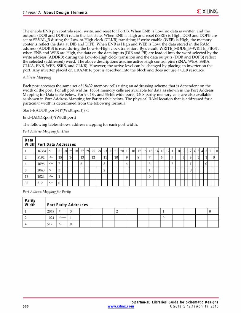
Chapter 2: About Design Elements
The enable ENB pin controls read, write, and reset for Port B. When ENB is Low, no data is written and theoutputs (DOB and DOPB) retain the last state. When ENB is High and reset (SSRB) is High, DOB and DOPB areset to SRVAL_B during the Low-to-High clock (CLKB) transition; if write enable (WEB) is High, the memorycontents reflect the data at DIB and DIPB. When ENB is High and WEB is Low, the data stored in the RAMaddress (ADDRB) is read during the Low-to-High clock transition. By default, WRITE_MODE_B=WRITE_FIRST,when ENB and WEB are High, the data on the data inputs (DIB and PB) are loaded into the word selected by thewrite address (ADDRB) during the Low-to-High clock transition and the data outputs (DOB and DOPB) reflectthe selected (addressed) word. The above descriptions assume active High control pins (ENA, WEA, SSRA,CLKA, ENB, WEB, SSRB, and CLKB). However, the active level can be changed by placing an inverter on theport. Any inverter placed on a RAMB16 port is absorbed into the block and does not use a CLB resource.
Address Mapping
Each port accesses the same set of 18432 memory cells using an addressing scheme that is dependent on thewidth of the port. For all port widths, 16384 memory cells are available for data as shown in the Port AddressMapping for Data table below. For 9-, 18-, and 36-bit wide ports, 2408 parity memory cells are also availableas shown in Port Address Mapping for Parity table below. The physical RAM location that is addressed for aparticular width is determined from the following formula.
Start=((ADDR port+1)*(Widthport)) -1
End=(ADDRport)*(Widthport)
The following tables shows address mapping for each port width.
Port Address Mapping for Data
DataWidth Port Data Addresses1 16384 <-- 31 30 29 28 27 26 25 24 23 22 21 20 19 18 17 16 15 14 13 12 11 10 9 8 7 6 5 4 3 2 1 0
2 8192 <-- 15 14 13 12 11 10 9 8 7 6 5 4 3 2 1 0
4 4096 <-- 7 6 5 4 3 2 1 0
8 2048 <-- 3 2 1 0
16 1024 <-- 1 0
32 512 <-- 0
Port Address Mapping for Parity
ParityWidth Port Parity Addresses1 2048 <----- 3 2 1 0
2 1024 <----- 1 0
4 512 <----- 0
Spartan-3E Libraries Guide for Schematic Designs500 www.xilinx.com UG618 (v 12.1) April 19, 2010

Chapter 2: About Design Elements
Initializing Memory Contents of a Dual-Port RAMB16
You can use the INIT_xx attributes to specify an initialization value for the memory contents of a RAMB16 duringdevice configuration. The initialization of each RAMB16_Sm_Sn is set by 64 initialization attributes (INIT_00through INIT_3F) of 64 hex values for a total of 16384 bits.
You can use the INITP_xx attributes to specify an initial value for the parity memory during device configurationor assertion. The initialization of the parity memory for ports configured for 9, 18, or 36 bits is set by 8initialization attributes (INITP_00 through INITP_07) of 64 hex values for a total of 2048 bits.
If any INIT_xx or INITP_xx attribute is not specified, it is configured as zeros. Partial Strings are padded withzeros to the left.
Initializing the Output Register of a Dual-Port RAMB16
In Spartan®-3A and above devices, each bit in an output register can be initialized at power on (when GSR ishigh) to either a 0 or 1. In addition, the initial state specified for power on can be different than the state thatresults from assertion of a set/reset. Four properties control initialization of the output register for a dual-portRAMB16: INIT_A, INIT_B, SRVAL_A, and SRVAL_B. The INIT_A attribute specifies the output register value atpower on for Port A and the INIT_B attribute specifies the value for Port B. You can use the SRVAL_A attribute todefine the state resulting from assertion of the SSR (set/reset) input on Port A. You can use the SRVAL_B attributeto define the state resulting from assertion of the SSR input on Port B.
The INIT_A, INIT_B, SRVAL_A, and SRVAL_B attributes specify the initialization value as a hexadecimal String.The value is dependent upon the port width. For example, for a RAMB16_S1_S4 with Port A width equal to 1and Port B width equal to 4, the Port A output register contains 1 bit and the Port B output register contains 4bits. Therefore, the INIT_A or SRVAL_A value can only be specified as a 1 or 0. For Port B, the output registercontains 4 bits. In this case, you can use INIT_B or SRVAL_B to specify a hexadecimal value from 0 through F toinitialize the 4 bits of the output register.
For those ports that include parity bits, the parity portion of the output register is specified in the high order bitposition of the INIT_A, INIT_B, SRVAL_A, or SRVAL_B value.
The INIT and SRVAL attributes default to zero if they are not set by you.
Write Mode Selection
TheWRITE_MODE_A attribute controls the memory and output contents of Port A for a dual-port RAMB16. TheWRITE_MODE_B attribute does the same for Port B. By default, both WRITE_MODE_A and WRITE_MODE_Bare set to WRITE_FIRST. This means that input is read, written to memory, and then passed to output. You canset the write mode for Port A and Port B to READ_FIRST to read the memory contents, pass the memory contentsto the outputs, and then write the input to memory. Or, you can set the write mode to NO_CHANGE to havethe input written to memory without changing the output. The Port A and Port B Conflict Resolution sectiondescribes how read/write conflicts are resolved when both Port A and Port B are attempting to read/write tothe same memory cells.
Port A and Port B Conflict Resolution
Spartan-3A block SelectRAM™ is True Dual-Port RAM that allows both ports to simultaneously access the samememory cell. When one port writes to a given memory cell, the other port must not address that memory cell (fora write or a read) within the clock-to-clock setup window.
The following tables summarize the collision detection behavior of the dual-port RAMB16 based on theWRITE_MODE_A and WRITE_MODE_B settings.
Spartan-3E Libraries Guide for Schematic DesignsUG618 (v 12.1) April 19, 2010 www.xilinx.com 501
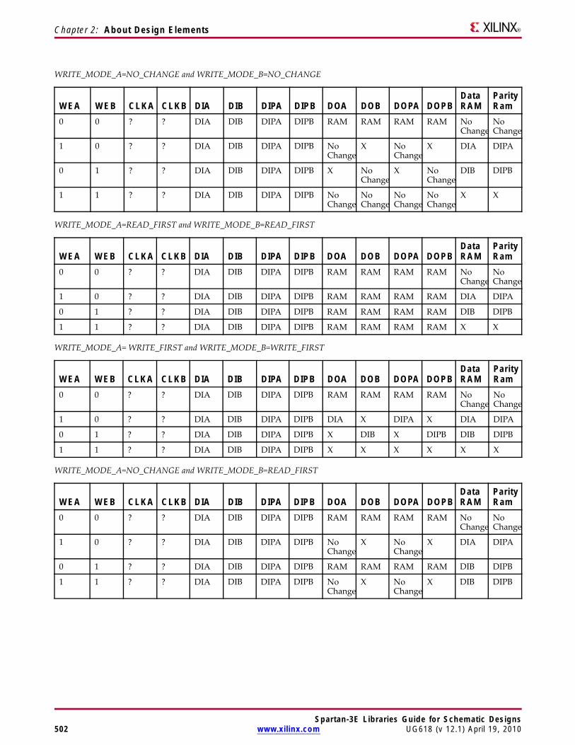
Chapter 2: About Design Elements
WRITE_MODE_A=NO_CHANGE and WRITE_MODE_B=NO_CHANGE
WEA WEB CLKA CLKB DIA DIB DIPA DIPB DOA DOB DOPA DOPBDataRAM
ParityRam
0 0 ? ? DIA DIB DIPA DIPB RAM RAM RAM RAM NoChange
NoChange
1 0 ? ? DIA DIB DIPA DIPB NoChange
X NoChange
X DIA DIPA
0 1 ? ? DIA DIB DIPA DIPB X NoChange
X NoChange
DIB DIPB
1 1 ? ? DIA DIB DIPA DIPB NoChange
NoChange
NoChange
NoChange
X X
WRITE_MODE_A=READ_FIRST and WRITE_MODE_B=READ_FIRST
WEA WEB CLKA CLKB DIA DIB DIPA DIPB DOA DOB DOPA DOPBDataRAM
ParityRam
0 0 ? ? DIA DIB DIPA DIPB RAM RAM RAM RAM NoChange
NoChange
1 0 ? ? DIA DIB DIPA DIPB RAM RAM RAM RAM DIA DIPA
0 1 ? ? DIA DIB DIPA DIPB RAM RAM RAM RAM DIB DIPB
1 1 ? ? DIA DIB DIPA DIPB RAM RAM RAM RAM X X
WRITE_MODE_A= WRITE_FIRST and WRITE_MODE_B=WRITE_FIRST
WEA WEB CLKA CLKB DIA DIB DIPA DIPB DOA DOB DOPA DOPBDataRAM
ParityRam
0 0 ? ? DIA DIB DIPA DIPB RAM RAM RAM RAM NoChange
NoChange
1 0 ? ? DIA DIB DIPA DIPB DIA X DIPA X DIA DIPA
0 1 ? ? DIA DIB DIPA DIPB X DIB X DIPB DIB DIPB
1 1 ? ? DIA DIB DIPA DIPB X X X X X X
WRITE_MODE_A=NO_CHANGE and WRITE_MODE_B=READ_FIRST
WEA WEB CLKA CLKB DIA DIB DIPA DIPB DOA DOB DOPA DOPBDataRAM
ParityRam
0 0 ? ? DIA DIB DIPA DIPB RAM RAM RAM RAM NoChange
NoChange
1 0 ? ? DIA DIB DIPA DIPB NoChange
X NoChange
X DIA DIPA
0 1 ? ? DIA DIB DIPA DIPB RAM RAM RAM RAM DIB DIPB
1 1 ? ? DIA DIB DIPA DIPB NoChange
X NoChange
X DIB DIPB
Spartan-3E Libraries Guide for Schematic Designs502 www.xilinx.com UG618 (v 12.1) April 19, 2010
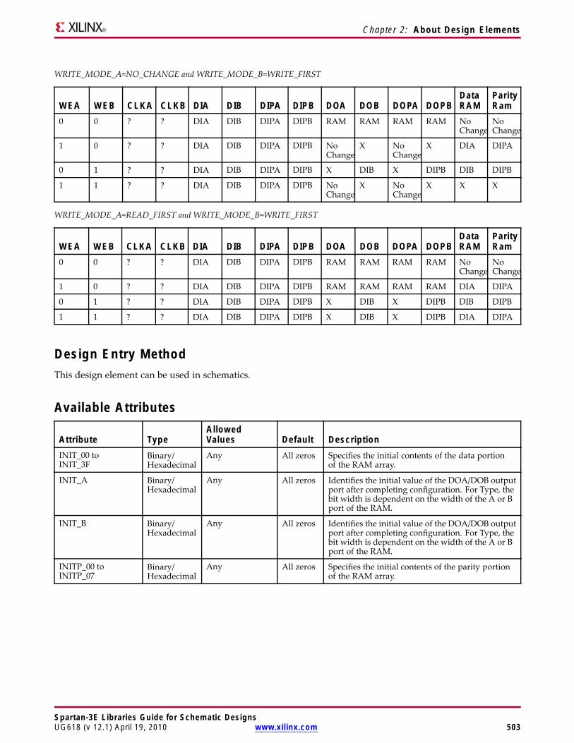
Chapter 2: About Design Elements
WRITE_MODE_A=NO_CHANGE and WRITE_MODE_B=WRITE_FIRST
WEA WEB CLKA CLKB DIA DIB DIPA DIPB DOA DOB DOPA DOPBDataRAM
ParityRam
0 0 ? ? DIA DIB DIPA DIPB RAM RAM RAM RAM NoChange
NoChange
1 0 ? ? DIA DIB DIPA DIPB NoChange
X NoChange
X DIA DIPA
0 1 ? ? DIA DIB DIPA DIPB X DIB X DIPB DIB DIPB
1 1 ? ? DIA DIB DIPA DIPB NoChange
X NoChange
X X X
WRITE_MODE_A=READ_FIRST and WRITE_MODE_B=WRITE_FIRST
WEA WEB CLKA CLKB DIA DIB DIPA DIPB DOA DOB DOPA DOPBDataRAM
ParityRam
0 0 ? ? DIA DIB DIPA DIPB RAM RAM RAM RAM NoChange
NoChange
1 0 ? ? DIA DIB DIPA DIPB RAM RAM RAM RAM DIA DIPA
0 1 ? ? DIA DIB DIPA DIPB X DIB X DIPB DIB DIPB
1 1 ? ? DIA DIB DIPA DIPB X DIB X DIPB DIA DIPA
Design Entry MethodThis design element can be used in schematics.
Available Attributes
Attribute TypeAllowedValues Default Description
INIT_00 toINIT_3F
Binary/Hexadecimal
Any All zeros Specifies the initial contents of the data portionof the RAM array.
INIT_A Binary/Hexadecimal
Any All zeros Identifies the initial value of the DOA/DOB outputport after completing configuration. For Type, thebit width is dependent on the width of the A or Bport of the RAM.
INIT_B Binary/Hexadecimal
Any All zeros Identifies the initial value of the DOA/DOB outputport after completing configuration. For Type, thebit width is dependent on the width of the A or Bport of the RAM.
INITP_00 toINITP_07
Binary/Hexadecimal
Any All zeros Specifies the initial contents of the parity portionof the RAM array.
Spartan-3E Libraries Guide for Schematic DesignsUG618 (v 12.1) April 19, 2010 www.xilinx.com 503
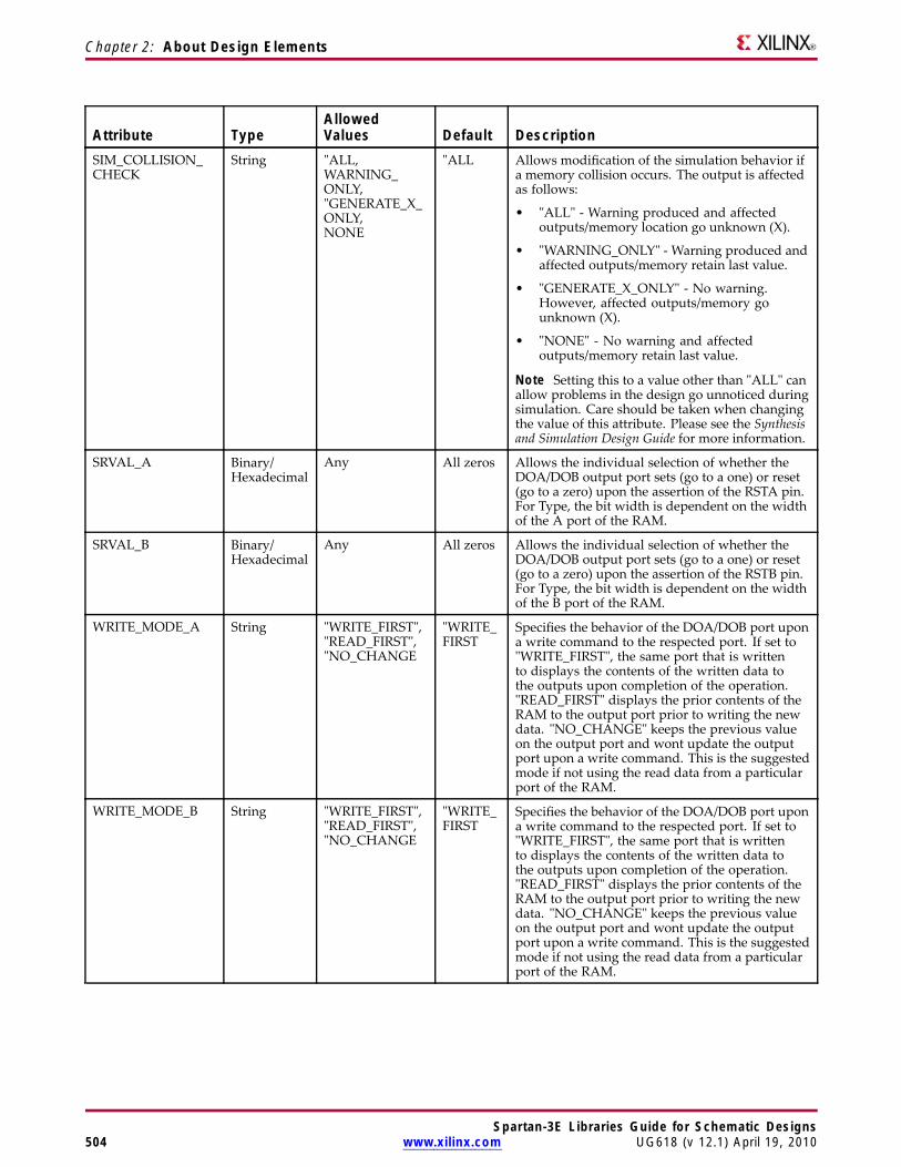
Chapter 2: About Design Elements
Attribute TypeAllowedValues Default Description
SIM_COLLISION_CHECK
String "ALL,WARNING_ONLY,"GENERATE_X_ONLY,NONE
"ALL Allows modification of the simulation behavior ifa memory collision occurs. The output is affectedas follows:
• "ALL" - Warning produced and affectedoutputs/memory location go unknown (X).
• "WARNING_ONLY" - Warning produced andaffected outputs/memory retain last value.
• "GENERATE_X_ONLY" - No warning.However, affected outputs/memory gounknown (X).
• "NONE" - No warning and affectedoutputs/memory retain last value.
Note Setting this to a value other than "ALL" canallow problems in the design go unnoticed duringsimulation. Care should be taken when changingthe value of this attribute. Please see the Synthesisand Simulation Design Guide for more information.
SRVAL_A Binary/Hexadecimal
Any All zeros Allows the individual selection of whether theDOA/DOB output port sets (go to a one) or reset(go to a zero) upon the assertion of the RSTA pin.For Type, the bit width is dependent on the widthof the A port of the RAM.
SRVAL_B Binary/Hexadecimal
Any All zeros Allows the individual selection of whether theDOA/DOB output port sets (go to a one) or reset(go to a zero) upon the assertion of the RSTB pin.For Type, the bit width is dependent on the widthof the B port of the RAM.
WRITE_MODE_A String "WRITE_FIRST","READ_FIRST","NO_CHANGE
"WRITE_FIRST
Specifies the behavior of the DOA/DOB port upona write command to the respected port. If set to"WRITE_FIRST", the same port that is writtento displays the contents of the written data tothe outputs upon completion of the operation."READ_FIRST" displays the prior contents of theRAM to the output port prior to writing the newdata. "NO_CHANGE" keeps the previous valueon the output port and wont update the outputport upon a write command. This is the suggestedmode if not using the read data from a particularport of the RAM.
WRITE_MODE_B String "WRITE_FIRST","READ_FIRST","NO_CHANGE
"WRITE_FIRST
Specifies the behavior of the DOA/DOB port upona write command to the respected port. If set to"WRITE_FIRST", the same port that is writtento displays the contents of the written data tothe outputs upon completion of the operation."READ_FIRST" displays the prior contents of theRAM to the output port prior to writing the newdata. "NO_CHANGE" keeps the previous valueon the output port and wont update the outputport upon a write command. This is the suggestedmode if not using the read data from a particularport of the RAM.
Spartan-3E Libraries Guide for Schematic Designs504 www.xilinx.com UG618 (v 12.1) April 19, 2010

Chapter 2: About Design Elements
For More Information• See the Spartan-3 Generation FPGA User Guide.
• See the Spartan-3E FPGA Family Complete Data Sheet.
Spartan-3E Libraries Guide for Schematic DesignsUG618 (v 12.1) April 19, 2010 www.xilinx.com 505

Spartan-3E Libraries Guide for Schematic Designs506 www.xilinx.com UG618 (v 12.1) April 19, 2010

Chapter 2: About Design Elements
RAMB16_S1_S18Primitive: 16K-bit Data and 2K-bit Parity Dual-Port Synchronous Block RAM with 1-bit and 18-bitPorts
IntroductionThis design element is a dual-ported dedicated random access memory block with synchronous write capability.Each block RAM port has 16384 bits of data memory. Ports configured as 9, 18, or 36 bits wide have an additional2048 bits of parity memory. Each port is independent of the other while accessing the same set of 16384 datamemory cells. Each port is independently configured to a specific data width. The possible port and cellconfigurations for this element are listed in the "Port Descriptions" section.
Spartan-3E Libraries Guide for Schematic DesignsUG618 (v 12.1) April 19, 2010 www.xilinx.com 507
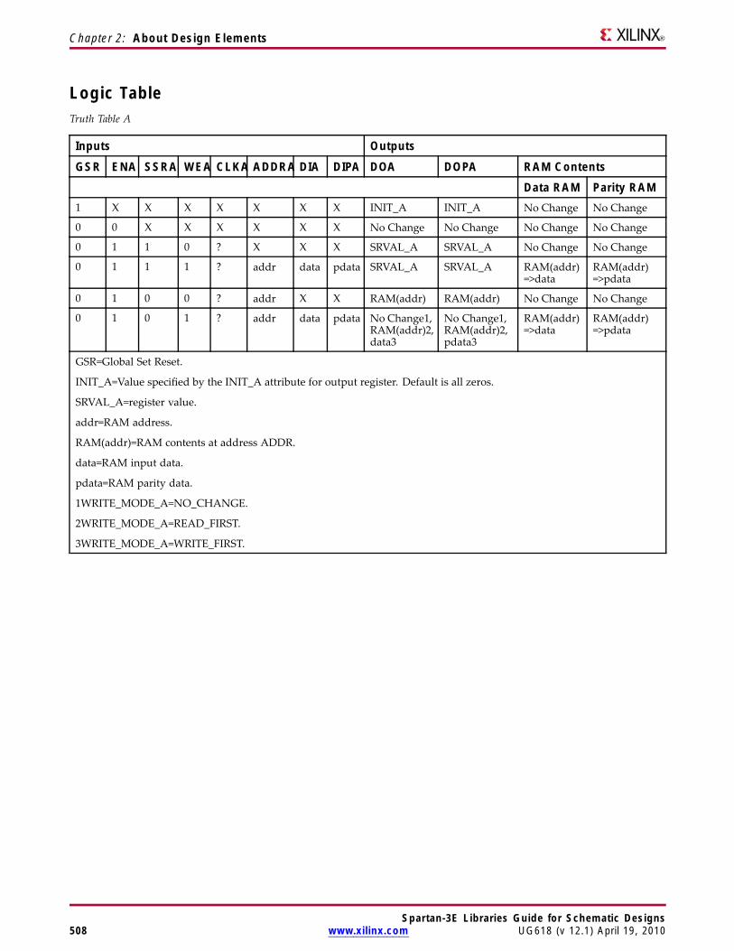
Chapter 2: About Design Elements
Logic TableTruth Table A
Inputs Outputs
GSR ENA SSRA WEA CLKA ADDRA DIA DIPA DOA DOPA RAM ContentsData RAM Parity RAM
1 X X X X X X X INIT_A INIT_A No Change No Change
0 0 X X X X X X No Change No Change No Change No Change
0 1 1 0 ? X X X SRVAL_A SRVAL_A No Change No Change
0 1 1 1 ? addr data pdata SRVAL_A SRVAL_A RAM(addr)=>data
RAM(addr)=>pdata
0 1 0 0 ? addr X X RAM(addr) RAM(addr) No Change No Change
0 1 0 1 ? addr data pdata No Change1,RAM(addr)2,data3
No Change1,RAM(addr)2,pdata3
RAM(addr)=>data
RAM(addr)=>pdata
GSR=Global Set Reset.
INIT_A=Value specified by the INIT_A attribute for output register. Default is all zeros.
SRVAL_A=register value.
addr=RAM address.
RAM(addr)=RAM contents at address ADDR.
data=RAM input data.
pdata=RAM parity data.
1WRITE_MODE_A=NO_CHANGE.
2WRITE_MODE_A=READ_FIRST.
3WRITE_MODE_A=WRITE_FIRST.
Spartan-3E Libraries Guide for Schematic Designs508 www.xilinx.com UG618 (v 12.1) April 19, 2010

Chapter 2: About Design Elements
Truth Table B
Inputs Outputs
GSR ENB SSRB WEB CLKB ADDRB DIB DIPB DOB DOPB RAM ContentsDataRAM
ParityRAM
1 X X X X X X X INIT_B INIT_B No Change No Change
0 0 X X X X X X No Change No Change No Change No Change
0 1 1 0 ? X X X SRVAL_B SRVAL_B No Change No Change
0 1 1 1 ? addr data pdata SRVAL_B SRVAL_B RAM(addr)=>data
RAM(addr)=>pdata
0 1 0 0 ? addr X X RAM(addr) RAM(addr) No Change No Change
0 1 0 1 ? addr data pdata No Change1,RAM(addr)=>data,data3
No Change1,RAM(addr)=>data,pdata3
RAM(addr)=>data
RAM(addr)=>pdata
GSR=Global Set Reset.
INIT_B=Value specified by the INIT_B attribute for output registers. Default is all zeros.
SRVAL_B=register value.
addr=RAM address.
RAM(addr)=RAM contents at address ADDR.
data=RAM input data.
pdata=RAM parity data.
1WRITE_MODE_B=NO_CHANGE.
2WRITE_MODE_B=READ_FIRST.
3WRITE_MODE_B=WRITE_FIRST.
Port DescriptionsPort A Port BDesignElement
DataCells(a)
ParityCells(a)
AddressBus
DataBus
ParityBus
DataCells(a)
ParityCells(a)
AddressBus
DataBus
ParityBus
RAMB16_S1_S18 16384 x1
- (13:0) (0:0) - 1024 x16
1024 x 2 (9:0) (15:0) (1:0)
(a) Depth x Width
Each port is fully synchronous with independent clock pins. All Port A input pins have setup time referencedto the CLKA pin and its data output bus DOA has a clock-to-out time referenced to the CLKA. All Port Binput pins have setup time referenced to the CLKB pin and its data output bus DOB has a clock-to-out timereferenced to the CLKB. The enable ENA pin controls read, write, and reset for Port A. When ENA is Low, nodata is written and the outputs (DOA and DOPA) retain the last state. When ENA is High and reset (SSRA) isHigh, DOA and DOPA are set to SRVAL_A during the Low-to-High clock (CLKA) transition; if write enable(WEA) is High, the memory contents reflect the data at DIA and DIPA. When ENA is High and WEA is Low,the data stored in the RAM address (ADDRA) is read during the Low-to-High clock transition. By default,WRITE_MODE_A=WRITE_FIRST, when ENA and WEA are High, the data on the data inputs (DIA and DIPA) isloaded into the word selected by the write address (ADDRA) during the Low-to-High clock transition and thedata outputs (DOA and DOPA) reflect the selected (addressed) word.
Spartan-3E Libraries Guide for Schematic DesignsUG618 (v 12.1) April 19, 2010 www.xilinx.com 509
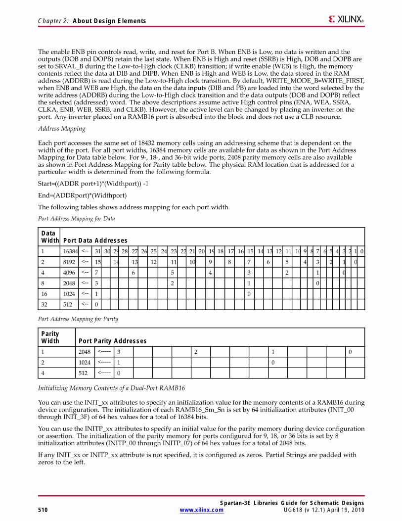
Chapter 2: About Design Elements
The enable ENB pin controls read, write, and reset for Port B. When ENB is Low, no data is written and theoutputs (DOB and DOPB) retain the last state. When ENB is High and reset (SSRB) is High, DOB and DOPB areset to SRVAL_B during the Low-to-High clock (CLKB) transition; if write enable (WEB) is High, the memorycontents reflect the data at DIB and DIPB. When ENB is High and WEB is Low, the data stored in the RAMaddress (ADDRB) is read during the Low-to-High clock transition. By default, WRITE_MODE_B=WRITE_FIRST,when ENB and WEB are High, the data on the data inputs (DIB and PB) are loaded into the word selected by thewrite address (ADDRB) during the Low-to-High clock transition and the data outputs (DOB and DOPB) reflectthe selected (addressed) word. The above descriptions assume active High control pins (ENA, WEA, SSRA,CLKA, ENB, WEB, SSRB, and CLKB). However, the active level can be changed by placing an inverter on theport. Any inverter placed on a RAMB16 port is absorbed into the block and does not use a CLB resource.
Address Mapping
Each port accesses the same set of 18432 memory cells using an addressing scheme that is dependent on thewidth of the port. For all port widths, 16384 memory cells are available for data as shown in the Port AddressMapping for Data table below. For 9-, 18-, and 36-bit wide ports, 2408 parity memory cells are also availableas shown in Port Address Mapping for Parity table below. The physical RAM location that is addressed for aparticular width is determined from the following formula.
Start=((ADDR port+1)*(Widthport)) -1
End=(ADDRport)*(Widthport)
The following tables shows address mapping for each port width.
Port Address Mapping for Data
DataWidth Port Data Addresses1 16384 <-- 31 30 29 28 27 26 25 24 23 22 21 20 19 18 17 16 15 14 13 12 11 10 9 8 7 6 5 4 3 2 1 0
2 8192 <-- 15 14 13 12 11 10 9 8 7 6 5 4 3 2 1 0
4 4096 <-- 7 6 5 4 3 2 1 0
8 2048 <-- 3 2 1 0
16 1024 <-- 1 0
32 512 <-- 0
Port Address Mapping for Parity
ParityWidth Port Parity Addresses1 2048 <----- 3 2 1 0
2 1024 <----- 1 0
4 512 <----- 0
Initializing Memory Contents of a Dual-Port RAMB16
You can use the INIT_xx attributes to specify an initialization value for the memory contents of a RAMB16 duringdevice configuration. The initialization of each RAMB16_Sm_Sn is set by 64 initialization attributes (INIT_00through INIT_3F) of 64 hex values for a total of 16384 bits.
You can use the INITP_xx attributes to specify an initial value for the parity memory during device configurationor assertion. The initialization of the parity memory for ports configured for 9, 18, or 36 bits is set by 8initialization attributes (INITP_00 through INITP_07) of 64 hex values for a total of 2048 bits.
If any INIT_xx or INITP_xx attribute is not specified, it is configured as zeros. Partial Strings are padded withzeros to the left.
Spartan-3E Libraries Guide for Schematic Designs510 www.xilinx.com UG618 (v 12.1) April 19, 2010
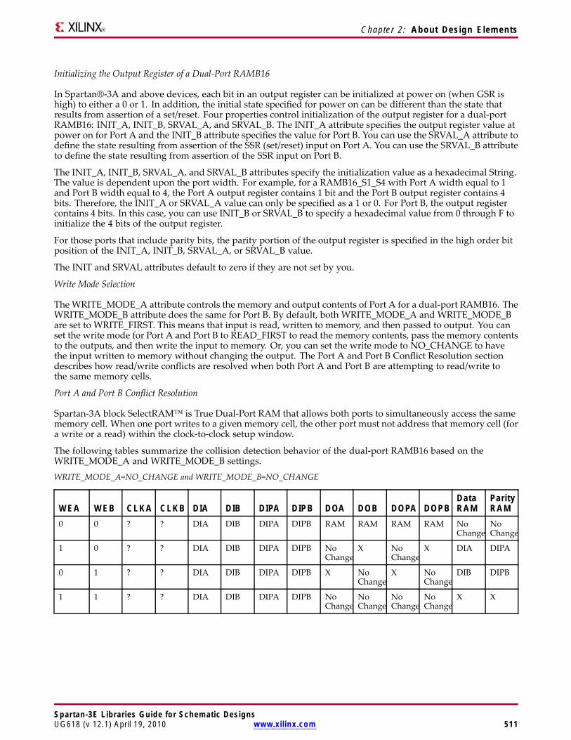
Chapter 2: About Design Elements
Initializing the Output Register of a Dual-Port RAMB16
In Spartan®-3A and above devices, each bit in an output register can be initialized at power on (when GSR ishigh) to either a 0 or 1. In addition, the initial state specified for power on can be different than the state thatresults from assertion of a set/reset. Four properties control initialization of the output register for a dual-portRAMB16: INIT_A, INIT_B, SRVAL_A, and SRVAL_B. The INIT_A attribute specifies the output register value atpower on for Port A and the INIT_B attribute specifies the value for Port B. You can use the SRVAL_A attribute todefine the state resulting from assertion of the SSR (set/reset) input on Port A. You can use the SRVAL_B attributeto define the state resulting from assertion of the SSR input on Port B.
The INIT_A, INIT_B, SRVAL_A, and SRVAL_B attributes specify the initialization value as a hexadecimal String.The value is dependent upon the port width. For example, for a RAMB16_S1_S4 with Port A width equal to 1and Port B width equal to 4, the Port A output register contains 1 bit and the Port B output register contains 4bits. Therefore, the INIT_A or SRVAL_A value can only be specified as a 1 or 0. For Port B, the output registercontains 4 bits. In this case, you can use INIT_B or SRVAL_B to specify a hexadecimal value from 0 through F toinitialize the 4 bits of the output register.
For those ports that include parity bits, the parity portion of the output register is specified in the high order bitposition of the INIT_A, INIT_B, SRVAL_A, or SRVAL_B value.
The INIT and SRVAL attributes default to zero if they are not set by you.
Write Mode Selection
TheWRITE_MODE_A attribute controls the memory and output contents of Port A for a dual-port RAMB16. TheWRITE_MODE_B attribute does the same for Port B. By default, both WRITE_MODE_A and WRITE_MODE_Bare set to WRITE_FIRST. This means that input is read, written to memory, and then passed to output. You canset the write mode for Port A and Port B to READ_FIRST to read the memory contents, pass the memory contentsto the outputs, and then write the input to memory. Or, you can set the write mode to NO_CHANGE to havethe input written to memory without changing the output. The Port A and Port B Conflict Resolution sectiondescribes how read/write conflicts are resolved when both Port A and Port B are attempting to read/write tothe same memory cells.
Port A and Port B Conflict Resolution
Spartan-3A block SelectRAM™ is True Dual-Port RAM that allows both ports to simultaneously access the samememory cell. When one port writes to a given memory cell, the other port must not address that memory cell (fora write or a read) within the clock-to-clock setup window.
The following tables summarize the collision detection behavior of the dual-port RAMB16 based on theWRITE_MODE_A and WRITE_MODE_B settings.
WRITE_MODE_A=NO_CHANGE and WRITE_MODE_B=NO_CHANGE
WEA WEB CLKA CLKB DIA DIB DIPA DIPB DOA DOB DOPA DOPBDataRAM
ParityRAM
0 0 ? ? DIA DIB DIPA DIPB RAM RAM RAM RAM NoChange
NoChange
1 0 ? ? DIA DIB DIPA DIPB NoChange
X NoChange
X DIA DIPA
0 1 ? ? DIA DIB DIPA DIPB X NoChange
X NoChange
DIB DIPB
1 1 ? ? DIA DIB DIPA DIPB NoChange
NoChange
NoChange
NoChange
X X
Spartan-3E Libraries Guide for Schematic DesignsUG618 (v 12.1) April 19, 2010 www.xilinx.com 511

Chapter 2: About Design Elements
WRITE_MODE_A=READ_FIRST and WRITE_MODE_B=READ_FIRST
WEA WEB CLKA CLKB DIA DIB DIPA DIPB DOA DOB DOPA DOPBDataRAM
ParityRAM
0 0 ? ? DIA DIB DIPA DIPB RAM RAM RAM RAM NoChange
NoChange
1 0 ? ? DIA DIB DIPA DIPB RAM RAM RAM RAM DIA DIPA
0 1 ? ? DIA DIB DIPA DIPB RAM RAM RAM RAM DIB DIPB
1 1 ? ? DIA DIB DIPA DIPB RAM RAM RAM RAM X X
WRITE_MODE_A= WRITE_FIRST and WRITE_MODE_B=WRITE_FIRST
WEA WEB CLKA CLKB DIA DIB DIPA DIPB DOA DOB DOPA DOPBDataRAM
ParityRAM
0 0 ? ? DIA DIB DIPA DIPB RAM RAM RAM RAM NoChange
NoChange
1 0 ? ? DIA DIB DIPA DIPB DIA X DIPA X DIA DIPA
0 1 ? ? DIA DIB DIPA DIPB X DIB X DIPB DIB DIPB
1 1 ? ? DIA DIB DIPA DIPB X X X X X X
WRITE_MODE_A=NO_CHANGE and WRITE_MODE_B=READ_FIRST
WEA WEB CLKA CLKB DIA DIB DIPA DIPB DOA DOB DOPA DOPBDataRAM
ParityRAM
0 0 ? ? DIA DIB DIPA DIPB RAM RAM RAM RAM NoChange
NoChange
1 0 ? ? DIA DIB DIPA DIPB NoChange
X NoChange
X DIA DIPA
0 1 ? ? DIA DIB DIPA DIPB RAM RAM RAM RAM DIB DIPB
1 1 ? ? DIA DIB DIPA DIPB NoChange
X NoChange
X DIB DIPB
WRITE_MODE_A=NO_CHANGE and WRITE_MODE_B=WRITE_FIRST
WEA WEB CLKA CLKB DIA DIB DIPA DIPB DOA DOB DOPA DOPBDataRAM
ParityRAM
0 0 ? ? DIA DIB DIPA DIPB RAM RAM RAM RAM NoChange
NoChange
1 0 ? ? DIA DIB DIPA DIPB NoChange
X NoChange
X DIA DIPA
0 1 ? ? DIA DIB DIPA DIPB X DIB X DIPB DIB DIPB
1 1 ? ? DIA DIB DIPA DIPB NoChange
X NoChange
X X X
Spartan-3E Libraries Guide for Schematic Designs512 www.xilinx.com UG618 (v 12.1) April 19, 2010
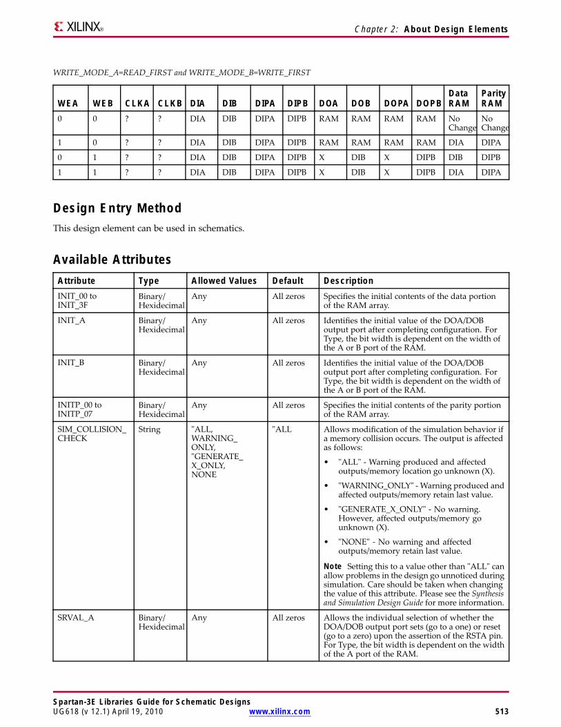
Chapter 2: About Design Elements
WRITE_MODE_A=READ_FIRST and WRITE_MODE_B=WRITE_FIRST
WEA WEB CLKA CLKB DIA DIB DIPA DIPB DOA DOB DOPA DOPBDataRAM
ParityRAM
0 0 ? ? DIA DIB DIPA DIPB RAM RAM RAM RAM NoChange
NoChange
1 0 ? ? DIA DIB DIPA DIPB RAM RAM RAM RAM DIA DIPA
0 1 ? ? DIA DIB DIPA DIPB X DIB X DIPB DIB DIPB
1 1 ? ? DIA DIB DIPA DIPB X DIB X DIPB DIA DIPA
Design Entry MethodThis design element can be used in schematics.
Available AttributesAttribute Type Allowed Values Default DescriptionINIT_00 toINIT_3F
Binary/Hexidecimal
Any All zeros Specifies the initial contents of the data portionof the RAM array.
INIT_A Binary/Hexidecimal
Any All zeros Identifies the initial value of the DOA/DOBoutput port after completing configuration. ForType, the bit width is dependent on the width ofthe A or B port of the RAM.
INIT_B Binary/Hexidecimal
Any All zeros Identifies the initial value of the DOA/DOBoutput port after completing configuration. ForType, the bit width is dependent on the width ofthe A or B port of the RAM.
INITP_00 toINITP_07
Binary/Hexidecimal
Any All zeros Specifies the initial contents of the parity portionof the RAM array.
SIM_COLLISION_CHECK
String "ALL,WARNING_ONLY,"GENERATE_X_ONLY,NONE
"ALL Allows modification of the simulation behavior ifa memory collision occurs. The output is affectedas follows:
• "ALL" - Warning produced and affectedoutputs/memory location go unknown (X).
• "WARNING_ONLY" - Warning produced andaffected outputs/memory retain last value.
• "GENERATE_X_ONLY" - No warning.However, affected outputs/memory gounknown (X).
• "NONE" - No warning and affectedoutputs/memory retain last value.
Note Setting this to a value other than "ALL" canallow problems in the design go unnoticed duringsimulation. Care should be taken when changingthe value of this attribute. Please see the Synthesisand Simulation Design Guide for more information.
SRVAL_A Binary/Hexidecimal
Any All zeros Allows the individual selection of whether theDOA/DOB output port sets (go to a one) or reset(go to a zero) upon the assertion of the RSTA pin.For Type, the bit width is dependent on the widthof the A port of the RAM.
Spartan-3E Libraries Guide for Schematic DesignsUG618 (v 12.1) April 19, 2010 www.xilinx.com 513
Chapter 2: About Design Elements
Attribute Type Allowed Values Default DescriptionSRVAL_B Binary/
HexidecimalAny All zeros Allows the individual selection of whether the
DOA/DOB output port sets (go to a one) or reset(go to a zero) upon the assertion of the RSTB pin.For Type, the bit width is dependent on the widthof the B port of the RAM.
WRITE_MODE_A String "WRITE_FIRST","READ_FIRST","NO_CHANGE
"WRITE_FIRST
Specifies the behavior of the DOA/DOB port upona write command to the respected port. If set to"WRITE_FIRST", the same port that is writtento displays the contents of the written data tothe outputs upon completion of the operation."READ_FIRST" displays the prior contents ofthe RAM to the output port prior to writing thenew data. "NO_CHANGE" keeps the previousvalue on the output port and wont update theoutput port upon a write command. This is thesuggested mode if not using the read data from aparticular port of the RAM.
WRITE_MODE_B String "WRITE_FIRST","READ_FIRST","NO_CHANGE
"WRITE_FIRST
Specifies the behavior of the DOA/DOB port upona write command to the respected port. If set to"WRITE_FIRST", the same port that is writtento displays the contents of the written data tothe outputs upon completion of the operation."READ_FIRST" displays the prior contents ofthe RAM to the output port prior to writing thenew data. "NO_CHANGE" keeps the previousvalue on the output port and wont update theoutput port upon a write command. This is thesuggested mode if not using the read data from aparticular port of the RAM.
For More Information• See the Spartan-3 Generation FPGA User Guide.
• See the Spartan-3E FPGA Family Complete Data Sheet.
Spartan-3E Libraries Guide for Schematic Designs514 www.xilinx.com UG618 (v 12.1) April 19, 2010

Spartan-3E Libraries Guide for Schematic Designs515 www.xilinx.com UG618 (v 12.1) April 19, 2010
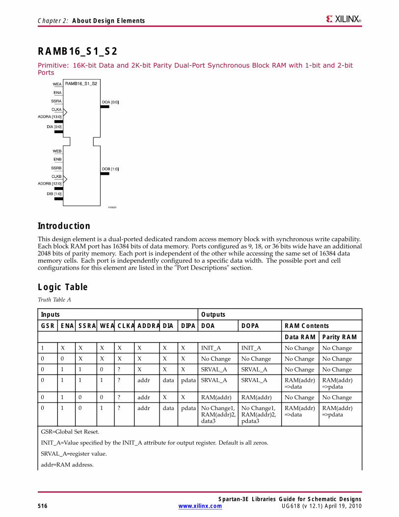
Chapter 2: About Design Elements
RAMB16_S1_S2Primitive: 16K-bit Data and 2K-bit Parity Dual-Port Synchronous Block RAM with 1-bit and 2-bitPorts
IntroductionThis design element is a dual-ported dedicated random access memory block with synchronous write capability.Each block RAM port has 16384 bits of data memory. Ports configured as 9, 18, or 36 bits wide have an additional2048 bits of parity memory. Each port is independent of the other while accessing the same set of 16384 datamemory cells. Each port is independently configured to a specific data width. The possible port and cellconfigurations for this element are listed in the "Port Descriptions" section.
Logic TableTruth Table A
Inputs Outputs
GSR ENA SSRA WEA CLKA ADDRA DIA DIPA DOA DOPA RAM ContentsData RAM Parity RAM
1 X X X X X X X INIT_A INIT_A No Change No Change
0 0 X X X X X X No Change No Change No Change No Change
0 1 1 0 ? X X X SRVAL_A SRVAL_A No Change No Change
0 1 1 1 ? addr data pdata SRVAL_A SRVAL_A RAM(addr)=>data
RAM(addr)=>pdata
0 1 0 0 ? addr X X RAM(addr) RAM(addr) No Change No Change
0 1 0 1 ? addr data pdata No Change1,RAM(addr)2,data3
No Change1,RAM(addr)2,pdata3
RAM(addr)=>data
RAM(addr)=>pdata
GSR=Global Set Reset.
INIT_A=Value specified by the INIT_A attribute for output register. Default is all zeros.
SRVAL_A=register value.
addr=RAM address.
Spartan-3E Libraries Guide for Schematic Designs516 www.xilinx.com UG618 (v 12.1) April 19, 2010

Chapter 2: About Design Elements
Inputs Outputs
GSR ENA SSRA WEA CLKA ADDRA DIA DIPA DOA DOPA RAM ContentsData RAM Parity RAM
RAM(addr)=RAM contents at address ADDR.
data=RAM input data.
pdata=RAM parity data.
1WRITE_MODE_A=NO_CHANGE.
2WRITE_MODE_A=READ_FIRST.
3WRITE_MODE_A=WRITE_FIRST.
Spartan-3E Libraries Guide for Schematic DesignsUG618 (v 12.1) April 19, 2010 www.xilinx.com 517

Chapter 2: About Design Elements
Truth Table B
Inputs Outputs
GSR ENB SSRB WEB CLKB ADDRB DIB DIPB DOB DOPB RAM ContentsDataRAM
ParityRAM
1 X X X X X X X INIT_B INIT_B No Change No Change
0 0 X X X X X X No Change No Change No Change No Change
0 1 1 0 ? X X X SRVAL_B SRVAL_B No Change No Change
0 1 1 1 ? addr data pdata SRVAL_B SRVAL_B RAM(addr)=>data
RAM(addr)=>pdata
0 1 0 0 ? addr X X RAM(addr) RAM(addr) No Change No Change
0 1 0 1 ? addr data pdata No Change1,RAM(addr)=>data,data3
No Change1,RAM(addr)=>data,pdata3
RAM(addr)=>data
RAM(addr)=>pdata
GSR=Global Set Reset.
INIT_B=Value specified by the INIT_B attribute for output registers. Default is all zeros.
SRVAL_B=register value.
addr=RAM address.
RAM(addr)=RAM contents at address ADDR.
data=RAM input data.
pdata=RAM parity data.
1WRITE_MODE_B=NO_CHANGE.
2WRITE_MODE_B=READ_FIRST.
3WRITE_MODE_B=WRITE_FIRST.
Port DescriptionsPort A Port BDesignElement
DataCells(a)
ParityCells(a)
AddressBus
DataBus
ParityBus
DataCells(a)
ParityCells(a)
AddressBus
DataBus
ParityBus
RAMB16_S1_S2 16384 x1
- (13:0) (0:0) - 8192 x 2 - (12:0) (1:0) -
(a)Depth x Width
Each port is fully synchronous with independent clock pins. All Port A input pins have setup time referencedto the CLKA pin and its data output bus DOA has a clock-to-out time referenced to the CLKA. All Port Binput pins have setup time referenced to the CLKB pin and its data output bus DOB has a clock-to-out timereferenced to the CLKB. The enable ENA pin controls read, write, and reset for Port A. When ENA is Low, nodata is written and the outputs (DOA and DOPA) retain the last state. When ENA is High and reset (SSRA) isHigh, DOA and DOPA are set to SRVAL_A during the Low-to-High clock (CLKA) transition; if write enable(WEA) is High, the memory contents reflect the data at DIA and DIPA. When ENA is High and WEA is Low,the data stored in the RAM address (ADDRA) is read during the Low-to-High clock transition. By default,WRITE_MODE_A=WRITE_FIRST, when ENA and WEA are High, the data on the data inputs (DIA and DIPA) isloaded into the word selected by the write address (ADDRA) during the Low-to-High clock transition and thedata outputs (DOA and DOPA) reflect the selected (addressed) word.
Spartan-3E Libraries Guide for Schematic Designs518 www.xilinx.com UG618 (v 12.1) April 19, 2010
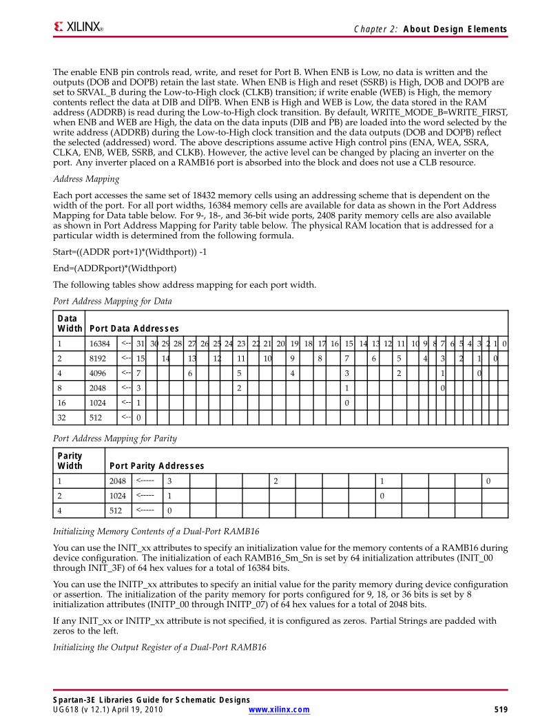
Chapter 2: About Design Elements
The enable ENB pin controls read, write, and reset for Port B. When ENB is Low, no data is written and theoutputs (DOB and DOPB) retain the last state. When ENB is High and reset (SSRB) is High, DOB and DOPB areset to SRVAL_B during the Low-to-High clock (CLKB) transition; if write enable (WEB) is High, the memorycontents reflect the data at DIB and DIPB. When ENB is High and WEB is Low, the data stored in the RAMaddress (ADDRB) is read during the Low-to-High clock transition. By default, WRITE_MODE_B=WRITE_FIRST,when ENB and WEB are High, the data on the data inputs (DIB and PB) are loaded into the word selected by thewrite address (ADDRB) during the Low-to-High clock transition and the data outputs (DOB and DOPB) reflectthe selected (addressed) word. The above descriptions assume active High control pins (ENA, WEA, SSRA,CLKA, ENB, WEB, SSRB, and CLKB). However, the active level can be changed by placing an inverter on theport. Any inverter placed on a RAMB16 port is absorbed into the block and does not use a CLB resource.
Address Mapping
Each port accesses the same set of 18432 memory cells using an addressing scheme that is dependent on thewidth of the port. For all port widths, 16384 memory cells are available for data as shown in the Port AddressMapping for Data table below. For 9-, 18-, and 36-bit wide ports, 2408 parity memory cells are also availableas shown in Port Address Mapping for Parity table below. The physical RAM location that is addressed for aparticular width is determined from the following formula.
Start=((ADDR port+1)*(Widthport)) -1
End=(ADDRport)*(Widthport)
The following tables show address mapping for each port width.
Port Address Mapping for Data
DataWidth Port Data Addresses1 16384 <-- 31 30 29 28 27 26 25 24 23 22 21 20 19 18 17 16 15 14 13 12 11 10 9 8 7 6 5 4 3 2 1 0
2 8192 <-- 15 14 13 12 11 10 9 8 7 6 5 4 3 2 1 0
4 4096 <-- 7 6 5 4 3 2 1 0
8 2048 <-- 3 2 1 0
16 1024 <-- 1 0
32 512 <-- 0
Port Address Mapping for Parity
ParityWidth Port Parity Addresses1 2048 <----- 3 2 1 0
2 1024 <----- 1 0
4 512 <----- 0
Initializing Memory Contents of a Dual-Port RAMB16
You can use the INIT_xx attributes to specify an initialization value for the memory contents of a RAMB16 duringdevice configuration. The initialization of each RAMB16_Sm_Sn is set by 64 initialization attributes (INIT_00through INIT_3F) of 64 hex values for a total of 16384 bits.
You can use the INITP_xx attributes to specify an initial value for the parity memory during device configurationor assertion. The initialization of the parity memory for ports configured for 9, 18, or 36 bits is set by 8initialization attributes (INITP_00 through INITP_07) of 64 hex values for a total of 2048 bits.
If any INIT_xx or INITP_xx attribute is not specified, it is configured as zeros. Partial Strings are padded withzeros to the left.
Initializing the Output Register of a Dual-Port RAMB16
Spartan-3E Libraries Guide for Schematic DesignsUG618 (v 12.1) April 19, 2010 www.xilinx.com 519
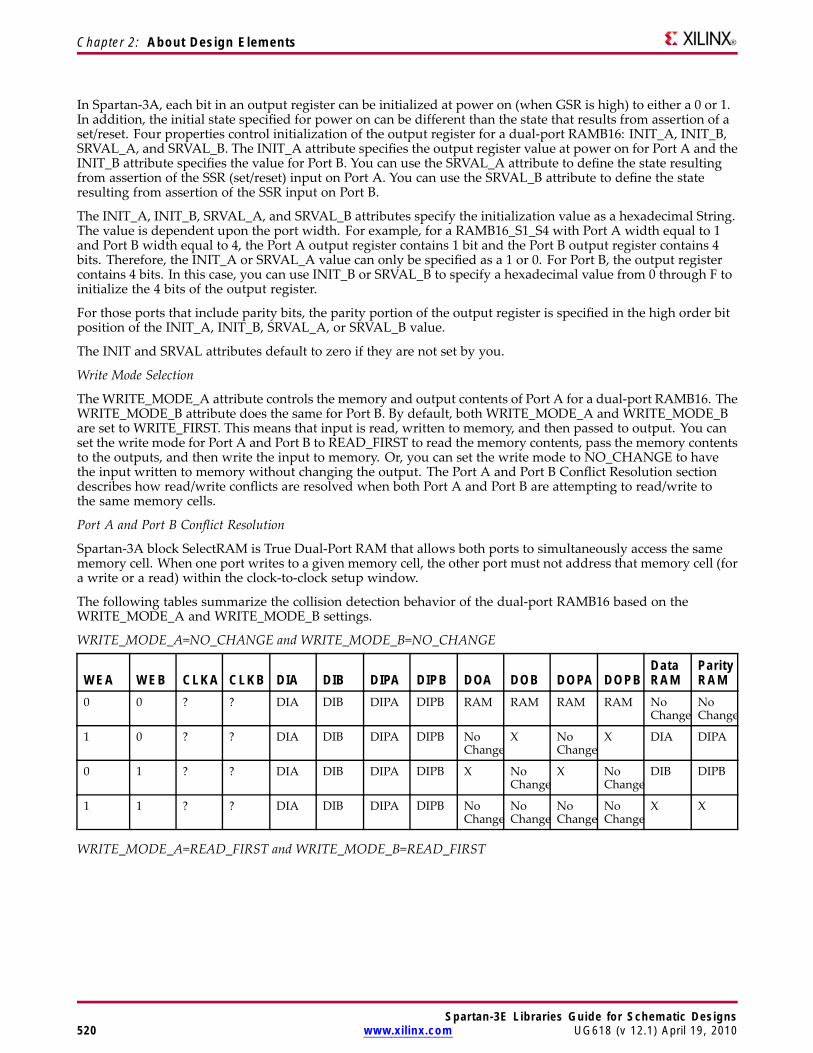
Chapter 2: About Design Elements
In Spartan-3A, each bit in an output register can be initialized at power on (when GSR is high) to either a 0 or 1.In addition, the initial state specified for power on can be different than the state that results from assertion of aset/reset. Four properties control initialization of the output register for a dual-port RAMB16: INIT_A, INIT_B,SRVAL_A, and SRVAL_B. The INIT_A attribute specifies the output register value at power on for Port A and theINIT_B attribute specifies the value for Port B. You can use the SRVAL_A attribute to define the state resultingfrom assertion of the SSR (set/reset) input on Port A. You can use the SRVAL_B attribute to define the stateresulting from assertion of the SSR input on Port B.
The INIT_A, INIT_B, SRVAL_A, and SRVAL_B attributes specify the initialization value as a hexadecimal String.The value is dependent upon the port width. For example, for a RAMB16_S1_S4 with Port A width equal to 1and Port B width equal to 4, the Port A output register contains 1 bit and the Port B output register contains 4bits. Therefore, the INIT_A or SRVAL_A value can only be specified as a 1 or 0. For Port B, the output registercontains 4 bits. In this case, you can use INIT_B or SRVAL_B to specify a hexadecimal value from 0 through F toinitialize the 4 bits of the output register.
For those ports that include parity bits, the parity portion of the output register is specified in the high order bitposition of the INIT_A, INIT_B, SRVAL_A, or SRVAL_B value.
The INIT and SRVAL attributes default to zero if they are not set by you.
Write Mode Selection
TheWRITE_MODE_A attribute controls the memory and output contents of Port A for a dual-port RAMB16. TheWRITE_MODE_B attribute does the same for Port B. By default, both WRITE_MODE_A and WRITE_MODE_Bare set to WRITE_FIRST. This means that input is read, written to memory, and then passed to output. You canset the write mode for Port A and Port B to READ_FIRST to read the memory contents, pass the memory contentsto the outputs, and then write the input to memory. Or, you can set the write mode to NO_CHANGE to havethe input written to memory without changing the output. The Port A and Port B Conflict Resolution sectiondescribes how read/write conflicts are resolved when both Port A and Port B are attempting to read/write tothe same memory cells.
Port A and Port B Conflict Resolution
Spartan-3A block SelectRAM is True Dual-Port RAM that allows both ports to simultaneously access the samememory cell. When one port writes to a given memory cell, the other port must not address that memory cell (fora write or a read) within the clock-to-clock setup window.
The following tables summarize the collision detection behavior of the dual-port RAMB16 based on theWRITE_MODE_A and WRITE_MODE_B settings.
WRITE_MODE_A=NO_CHANGE and WRITE_MODE_B=NO_CHANGE
WEA WEB CLKA CLKB DIA DIB DIPA DIPB DOA DOB DOPA DOPBDataRAM
ParityRAM
0 0 ? ? DIA DIB DIPA DIPB RAM RAM RAM RAM NoChange
NoChange
1 0 ? ? DIA DIB DIPA DIPB NoChange
X NoChange
X DIA DIPA
0 1 ? ? DIA DIB DIPA DIPB X NoChange
X NoChange
DIB DIPB
1 1 ? ? DIA DIB DIPA DIPB NoChange
NoChange
NoChange
NoChange
X X
WRITE_MODE_A=READ_FIRST and WRITE_MODE_B=READ_FIRST
Spartan-3E Libraries Guide for Schematic Designs520 www.xilinx.com UG618 (v 12.1) April 19, 2010
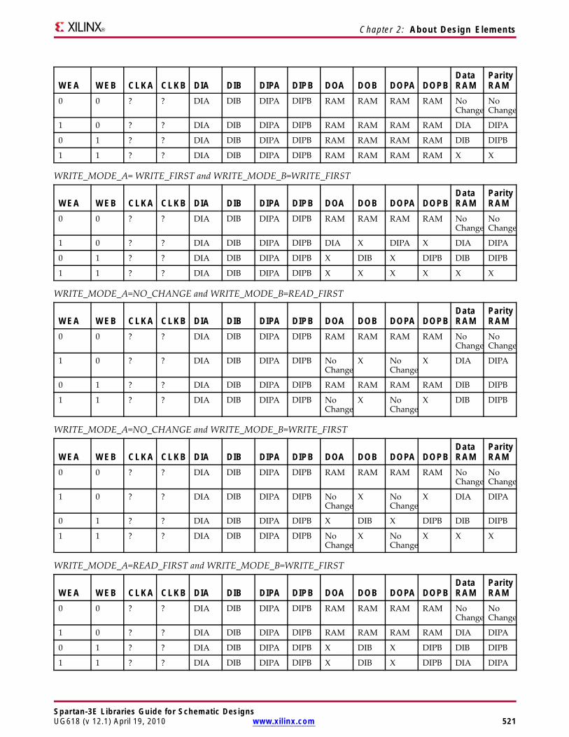
Chapter 2: About Design Elements
WEA WEB CLKA CLKB DIA DIB DIPA DIPB DOA DOB DOPA DOPBDataRAM
ParityRAM
0 0 ? ? DIA DIB DIPA DIPB RAM RAM RAM RAM NoChange
NoChange
1 0 ? ? DIA DIB DIPA DIPB RAM RAM RAM RAM DIA DIPA
0 1 ? ? DIA DIB DIPA DIPB RAM RAM RAM RAM DIB DIPB
1 1 ? ? DIA DIB DIPA DIPB RAM RAM RAM RAM X X
WRITE_MODE_A= WRITE_FIRST and WRITE_MODE_B=WRITE_FIRST
WEA WEB CLKA CLKB DIA DIB DIPA DIPB DOA DOB DOPA DOPBDataRAM
ParityRAM
0 0 ? ? DIA DIB DIPA DIPB RAM RAM RAM RAM NoChange
NoChange
1 0 ? ? DIA DIB DIPA DIPB DIA X DIPA X DIA DIPA
0 1 ? ? DIA DIB DIPA DIPB X DIB X DIPB DIB DIPB
1 1 ? ? DIA DIB DIPA DIPB X X X X X X
WRITE_MODE_A=NO_CHANGE and WRITE_MODE_B=READ_FIRST
WEA WEB CLKA CLKB DIA DIB DIPA DIPB DOA DOB DOPA DOPBDataRAM
ParityRAM
0 0 ? ? DIA DIB DIPA DIPB RAM RAM RAM RAM NoChange
NoChange
1 0 ? ? DIA DIB DIPA DIPB NoChange
X NoChange
X DIA DIPA
0 1 ? ? DIA DIB DIPA DIPB RAM RAM RAM RAM DIB DIPB
1 1 ? ? DIA DIB DIPA DIPB NoChange
X NoChange
X DIB DIPB
WRITE_MODE_A=NO_CHANGE and WRITE_MODE_B=WRITE_FIRST
WEA WEB CLKA CLKB DIA DIB DIPA DIPB DOA DOB DOPA DOPBDataRAM
ParityRAM
0 0 ? ? DIA DIB DIPA DIPB RAM RAM RAM RAM NoChange
NoChange
1 0 ? ? DIA DIB DIPA DIPB NoChange
X NoChange
X DIA DIPA
0 1 ? ? DIA DIB DIPA DIPB X DIB X DIPB DIB DIPB
1 1 ? ? DIA DIB DIPA DIPB NoChange
X NoChange
X X X
WRITE_MODE_A=READ_FIRST and WRITE_MODE_B=WRITE_FIRST
WEA WEB CLKA CLKB DIA DIB DIPA DIPB DOA DOB DOPA DOPBDataRAM
ParityRAM
0 0 ? ? DIA DIB DIPA DIPB RAM RAM RAM RAM NoChange
NoChange
1 0 ? ? DIA DIB DIPA DIPB RAM RAM RAM RAM DIA DIPA
0 1 ? ? DIA DIB DIPA DIPB X DIB X DIPB DIB DIPB
1 1 ? ? DIA DIB DIPA DIPB X DIB X DIPB DIA DIPA
Spartan-3E Libraries Guide for Schematic DesignsUG618 (v 12.1) April 19, 2010 www.xilinx.com 521

Chapter 2: About Design Elements
Design Entry MethodThis design element can be used in schematics.
Available Attributes
Attribute TypeAllowedValues Default Description
INIT_00 toINIT_3F
Binary/Hexadecimal
Any All zeros Specifies the initial contents of the data portionof the RAM array.
INIT_A Binary/Hexadecimal
Any All zeros Identifies the initial value of the DOA/DOB outputport after completing configuration. For Type, thebit width is dependent on the width of the A or Bport of the RAM.
INIT_B Binary/Hexadecimal
Any All zeros Identifies the initial value of the DOA/DOB outputport after completing configuration. For Type, thebit width is dependent on the width of the A or Bport of the RAM.
INITP_00 toINITP_07
Binary/Hexadecimal
Any All zeros Specifies the initial contents of the parity portionof the RAM array.
SIM_COLLISION_CHECK
String "ALL,WARNING_ONLY,"GENERATE_X_ONLY,NONE
"ALL Allows modification of the simulation behavior ifa memory collision occurs. The output is affectedas follows:
• "ALL" - Warning produced and affectedoutputs/memory location go unknown (X).
• "WARNING_ONLY" - Warning produced andaffected outputs/memory retain last value.
• "GENERATE_X_ONLY" - No warning.However, affected outputs/memory gounknown (X).
• "NONE" - No warning and affectedoutputs/memory retain last value.
Note Setting this to a value other than "ALL" canallow problems in the design go unnoticed duringsimulation. Care should be taken when changingthe value of this attribute. Please see the Synthesisand Simulation Design Guide for more information.
SRVAL_A Binary/Hexadecimal
Any All zeros Allows the individual selection of whether theDOA/DOB output port sets (go to a one) or reset(go to a zero) upon the assertion of the RSTA pin.For Type, the bit width is dependent on the widthof the A port of the RAM.
SRVAL_B Binary/Hexadecimal
Any All zeros Allows the individual selection of whether theDOA/DOB output port sets (go to a one) or reset(go to a zero) upon the assertion of the RSTB pin.For Type, the bit width is dependent on the widthof the B port of the RAM.
Spartan-3E Libraries Guide for Schematic Designs522 www.xilinx.com UG618 (v 12.1) April 19, 2010

Chapter 2: About Design Elements
Attribute TypeAllowedValues Default Description
WRITE_MODE_A String "WRITE_FIRST","READ_FIRST","NO_CHANGE
"WRITE_FIRST
Specifies the behavior of the DOA/DOB port upona write command to the respected port. If set to"WRITE_FIRST", the same port that is writtento displays the contents of the written data tothe outputs upon completion of the operation."READ_FIRST" displays the prior contents of theRAM to the output port prior to writing the newdata. "NO_CHANGE" keeps the previous valueon the output port and wont update the outputport upon a write command. This is the suggestedmode if not using the read data from a particularport of the RAM.
WRITE_MODE_B String "WRITE_FIRST","READ_FIRST","NO_CHANGE
"WRITE_FIRST
Specifies the behavior of the DOA/DOB port upona write command to the respected port. If set to"WRITE_FIRST", the same port that is writtento displays the contents of the written data tothe outputs upon completion of the operation."READ_FIRST" displays the prior contents of theRAM to the output port prior to writing the newdata. "NO_CHANGE" keeps the previous valueon the output port and wont update the outputport upon a write command. This is the suggestedmode if not using the read data from a particularport of the RAM.
For More Information• See the Spartan-3 Generation FPGA User Guide.
• See the Spartan-3E FPGA Family Complete Data Sheet.
Spartan-3E Libraries Guide for Schematic DesignsUG618 (v 12.1) April 19, 2010 www.xilinx.com 523

Spartan-3E Libraries Guide for Schematic Designs524 www.xilinx.com UG618 (v 12.1) April 19, 2010
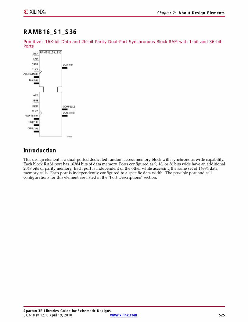
Chapter 2: About Design Elements
RAMB16_S1_S36Primitive: 16K-bit Data and 2K-bit Parity Dual-Port Synchronous Block RAM with 1-bit and 36-bitPorts
IntroductionThis design element is a dual-ported dedicated random access memory block with synchronous write capability.Each block RAM port has 16384 bits of data memory. Ports configured as 9, 18, or 36 bits wide have an additional2048 bits of parity memory. Each port is independent of the other while accessing the same set of 16384 datamemory cells. Each port is independently configured to a specific data width. The possible port and cellconfigurations for this element are listed in the "Port Descriptions" section.
Spartan-3E Libraries Guide for Schematic DesignsUG618 (v 12.1) April 19, 2010 www.xilinx.com 525

Chapter 2: About Design Elements
Logic TableTruth Table A
Inputs Outputs
GSR ENA SSRA WEA CLKA ADDRA DIA DIPA DOA DOPA RAM ContentsData RAM Parity RAM
1 X X X X X X X INIT_A INIT_A No Change No Change
0 0 X X X X X X No Change No Change No Change No Change
0 1 1 0 ? X X X SRVAL_A SRVAL_A No Change No Change
0 1 1 1 ? addr data pdata SRVAL_A SRVAL_A RAM(addr)=>data
RAM(addr)=>pdata
0 1 0 0 ? addr X X RAM(addr) RAM(addr) No Change No Change
0 1 0 1 ? addr data pdata No Change1,RAM(addr)2,data3
No Change1,RAM(addr)2,pdata3
RAM(addr)=>data
RAM(addr)=>pdata
GSR=Global Set Reset.
INIT_A=Value specified by the INIT_A attribute for output register. Default is all zeros.
SRVAL_A=register value.
addr=RAM address.
RAM(addr)=RAM contents at address ADDR.
data=RAM input data.
pdata=RAM parity data.
1WRITE_MODE_A=NO_CHANGE.
2WRITE_MODE_A=READ_FIRST.
3WRITE_MODE_A=WRITE_FIRST.
Spartan-3E Libraries Guide for Schematic Designs526 www.xilinx.com UG618 (v 12.1) April 19, 2010
Chapter 2: About Design Elements
Truth Table B
Inputs Outputs
GSR ENB SSRB WEB CLKB ADDRB DIB DIPB DOB DOPB RAM ContentsDataRAM
ParityRAM
1 X X X X X X X INIT_B INIT_B No Change No Change
0 0 X X X X X X No Change No Change No Change No Change
0 1 1 0 ? X X X SRVAL_B SRVAL_B No Change No Change
0 1 1 1 ? addr data pdata SRVAL_B SRVAL_B RAM(addr)=>data
RAM(addr)=>pdata
0 1 0 0 ? addr X X RAM(addr) RAM(addr) No Change No Change
0 1 0 1 ? addr data pdata No Change1,RAM(addr)=>data,data3
No Change1,RAM(addr)=>data,pdata3
RAM(addr)=>data
RAM(addr)=>pdata
GSR=Global Set Reset.
INIT_B=Value specified by the INIT_B attribute for output registers. Default is all zeros.
SRVAL_B=register value.
addr=RAM address.
RAM(addr)=RAM contents at address ADDR.
data=RAM input data.
pdata=RAM parity data.
1WRITE_MODE_B=NO_CHANGE.
2WRITE_MODE_B=READ_FIRST.
3WRITE_MODE_B=WRITE_FIRST.
Port DescriptionsPort A Port BDesignElement
DataCells(a)
ParityCells(a)
AddressBus
DataBus
ParityBus
DataCells(a)
ParityCells(a)
AddressBus
DataBus
ParityBus
RAMB16_S1_S36 16384 x1
- (13:0) (0:0) - 512 x 32 512 x 4 (8:0) (31:0) (3:0)
(a) Depth x Width
Each port is fully synchronous with independent clock pins. All Port A input pins have setup time referencedto the CLKA pin and its data output bus DOA has a clock-to-out time referenced to the CLKA. All Port Binput pins have setup time referenced to the CLKB pin and its data output bus DOB has a clock-to-out timereferenced to the CLKB. The enable ENA pin controls read, write, and reset for Port A. When ENA is Low, nodata is written and the outputs (DOA and DOPA) retain the last state. When ENA is High and reset (SSRA) isHigh, DOA and DOPA are set to SRVAL_A during the Low-to-High clock (CLKA) transition; if write enable(WEA) is High, the memory contents reflect the data at DIA and DIPA. When ENA is High and WEA is Low,the data stored in the RAM address (ADDRA) is read during the Low-to-High clock transition. By default,WRITE_MODE_A=WRITE_FIRST, when ENA and WEA are High, the data on the data inputs (DIA and DIPA) isloaded into the word selected by the write address (ADDRA) during the Low-to-High clock transition and thedata outputs (DOA and DOPA) reflect the selected (addressed) word.
Spartan-3E Libraries Guide for Schematic DesignsUG618 (v 12.1) April 19, 2010 www.xilinx.com 527

Chapter 2: About Design Elements
The enable ENB pin controls read, write, and reset for Port B. When ENB is Low, no data is written and theoutputs (DOB and DOPB) retain the last state. When ENB is High and reset (SSRB) is High, DOB and DOPB areset to SRVAL_B during the Low-to-High clock (CLKB) transition; if write enable (WEB) is High, the memorycontents reflect the data at DIB and DIPB. When ENB is High and WEB is Low, the data stored in the RAMaddress (ADDRB) is read during the Low-to-High clock transition. By default, WRITE_MODE_B=WRITE_FIRST,when ENB and WEB are High, the data on the data inputs (DIB and PB) are loaded into the word selected by thewrite address (ADDRB) during the Low-to-High clock transition and the data outputs (DOB and DOPB) reflectthe selected (addressed) word. The above descriptions assume active High control pins (ENA, WEA, SSRA,CLKA, ENB, WEB, SSRB, and CLKB). However, the active level can be changed by placing an inverter on theport. Any inverter placed on a RAMB16 port is absorbed into the block and does not use a CLB resource.
Address Mapping
Each port accesses the same set of 18432 memory cells using an addressing scheme that is dependent on thewidth of the port. For all port widths, 16384 memory cells are available for data as shown in the Port AddressMapping for Data table below. For 9-, 18-, and 36-bit wide ports, 2408 parity memory cells are also availableas shown in Port Address Mapping for Parity table below. The physical RAM location that is addressed for aparticular width is determined from the following formula.
Start=((ADDR port+1)*(Widthport)) -1
End=(ADDRport)*(Widthport)
The following tables show address mapping for each port width.
Port Address Mapping for Data
DataWidth Port Data Addresses1 16384 <-- 31 30 29 28 27 26 25 24 23 22 21 20 19 18 17 16 15 14 13 12 11 10 9 8 7 6 5 4 3 2 1 0
2 8192 <-- 15 14 13 12 11 10 9 8 7 6 5 4 3 2 1 0
4 4096 <-- 7 6 5 4 3 2 1 0
8 2048 <-- 3 2 1 0
16 1024 <-- 1 0
32 512 <-- 0
Port Address Mapping for Parity
ParityWidth Port Parity Addresses1 2048 <---- 3 2 1 0
2 1024 <---- 1 0
4 512 <---- 0
Initializing Memory Contents of a Dual-Port RAMB16
You can use the INIT_xx attributes to specify an initialization value for the memory contents of a RAMB16 duringdevice configuration. The initialization of each RAMB16_Sm_Sn is set by 64 initialization attributes (INIT_00through INIT_3F) of 64 hex values for a total of 16384 bits.
You can use the INITP_xx attributes to specify an initial value for the parity memory during device configurationor assertion. The initialization of the parity memory for ports configured for 9, 18, or 36 bits is set by 8initialization attributes (INITP_00 through INITP_07) of 64 hex values for a total of 2048 bits.
If any INIT_xx or INITP_xx attribute is not specified, it is configured as zeros. Partial Strings are padded withzeros to the left.
Spartan-3E Libraries Guide for Schematic Designs528 www.xilinx.com UG618 (v 12.1) April 19, 2010

Chapter 2: About Design Elements
Initializing the Output Register of a Dual-Port RAMB16
In Spartan®-3A and above devices, each bit in an output register can be initialized at power on (when GSR ishigh) to either a 0 or 1. In addition, the initial state specified for power on can be different than the state thatresults from assertion of a set/reset. Four properties control initialization of the output register for a dual-portRAMB16: INIT_A, INIT_B, SRVAL_A, and SRVAL_B. The INIT_A attribute specifies the output register value atpower on for Port A and the INIT_B attribute specifies the value for Port B. You can use the SRVAL_A attribute todefine the state resulting from assertion of the SSR (set/reset) input on Port A. You can use the SRVAL_B attributeto define the state resulting from assertion of the SSR input on Port B.
The INIT_A, INIT_B, SRVAL_A, and SRVAL_B attributes specify the initialization value as a hexadecimal String.The value is dependent upon the port width. For example, for a RAMB16_S1_S4 with Port A width equal to 1and Port B width equal to 4, the Port A output register contains 1 bit and the Port B output register contains 4bits. Therefore, the INIT_A or SRVAL_A value can only be specified as a 1 or 0. For Port B, the output registercontains 4 bits. In this case, you can use INIT_B or SRVAL_B to specify a hexadecimal value from 0 through F toinitialize the 4 bits of the output register.
For those ports that include parity bits, the parity portion of the output register is specified in the high order bitposition of the INIT_A, INIT_B, SRVAL_A, or SRVAL_B value.
The INIT and SRVAL attributes default to zero if they are not set by you.
Write Mode Selection
TheWRITE_MODE_A attribute controls the memory and output contents of Port A for a dual-port RAMB16. TheWRITE_MODE_B attribute does the same for Port B. By default, both WRITE_MODE_A and WRITE_MODE_Bare set to WRITE_FIRST. This means that input is read, written to memory, and then passed to output. You canset the write mode for Port A and Port B to READ_FIRST to read the memory contents, pass the memory contentsto the outputs, and then write the input to memory. Or, you can set the write mode to NO_CHANGE to havethe input written to memory without changing the output. The Port A and Port B Conflict Resolution sectiondescribes how read/write conflicts are resolved when both Port A and Port B are attempting to read/write tothe same memory cells.
Port A and Port B Conflict Resolution
Spartan-3A block SelectRAM™ is True Dual-Port RAM that allows both ports to simultaneously access the samememory cell. When one port writes to a given memory cell, the other port must not address that memory cell (fora write or a read) within the clock-to-clock setup window.
The following tables summarize the collision detection behavior of the dual-port RAMB16 based on theWRITE_MODE_A and WRITE_MODE_B settings.
WRITE_MODE_A=NO_CHANGE and WRITE_MODE_B=NO_CHANGE
WEA WEB CLKA CLKB DIA DIB DIPA DIPB DOA DOB DOPA DOPBDataRAM
ParityRAM
0 0 ? ? DIA DIB DIPA DIPB RAM RAM RAM RAM NoChange
NoChange
1 0 ? ? DIA DIB DIPA DIPB NoChange
X NoChange
X DIA DIPA
0 1 ? ? DIA DIB DIPA DIPB X NoChange
X NoChange
DIB DIPB
1 1 ? ? DIA DIB DIPA DIPB NoChange
NoChange
NoChange
NoChange
X X
Spartan-3E Libraries Guide for Schematic DesignsUG618 (v 12.1) April 19, 2010 www.xilinx.com 529

Chapter 2: About Design Elements
WRITE_MODE_A=READ_FIRST and WRITE_MODE_B=READ_FIRST
WEA WEB CLKA CLKB DIA DIB DIPA DIPB DOA DOB DOPA DOPBDataRAM
ParityRAM
0 0 ? ? DIA DIB DIPA DIPB RAM RAM RAM RAM NoChange
NoChange
1 0 ? ? DIA DIB DIPA DIPB RAM RAM RAM RAM DIA DIPA
0 1 ? ? DIA DIB DIPA DIPB RAM RAM RAM RAM DIB DIPB
1 1 ? ? DIA DIB DIPA DIPB RAM RAM RAM RAM X X
WRITE_MODE_A= WRITE_FIRST and WRITE_MODE_B=WRITE_FIRST
WEA WEB CLKA CLKB DIA DIB DIPA DIPB DOA DOB DOPA DOPBDataRAM
ParityRAM
0 0 ? ? DIA DIB DIPA DIPB RAM RAM RAM RAM NoChange
NoChange
1 0 ? ? DIA DIB DIPA DIPB DIA X DIPA X DIA DIPA
0 1 ? ? DIA DIB DIPA DIPB X DIB X DIPB DIB DIPB
1 1 ? ? DIA DIB DIPA DIPB X X X X X X
WRITE_MODE_A=NO_CHANGE and WRITE_MODE_B=READ_FIRST
WEA WEB CLKA CLKB DIA DIB DIPA DIPB DOA DOB DOPA DOPBDataRAM
ParityRAM
0 0 ? ? DIA DIB DIPA DIPB RAM RAM RAM RAM NoChange
NoChange
1 0 ? ? DIA DIB DIPA DIPB NoChange
X NoChange
X DIA DIPA
0 1 ? ? DIA DIB DIPA DIPB RAM RAM RAM RAM DIB DIPB
1 1 ? ? DIA DIB DIPA DIPB NoChange
X NoChange
X DIB DIPB
WRITE_MODE_A=NO_CHANGE and WRITE_MODE_B=WRITE_FIRST
WEA WEB CLKA CLKB DIA DIB DIPA DIPB DOA DOB DOPA DOPBDataRAM
ParityRAM
0 0 ? ? DIA DIB DIPA DIPB RAM RAM RAM RAM NoChange
NoChange
1 0 ? ? DIA DIB DIPA DIPB NoChange
X NoChange
X DIA DIPA
0 1 ? ? DIA DIB DIPA DIPB X DIB X DIPB DIB DIPB
1 1 ? ? DIA DIB DIPA DIPB NoChange
X NoChange
X X X
Spartan-3E Libraries Guide for Schematic Designs530 www.xilinx.com UG618 (v 12.1) April 19, 2010

Chapter 2: About Design Elements
WRITE_MODE_A=READ_FIRST and WRITE_MODE_B=WRITE_FIRST
WEA WEB CLKA CLKB DIA DIB DIPA DIPB DOA DOB DOPA DOPBDataRAM
ParityRAM
0 0 ? ? DIA DIB DIPA DIPB RAM RAM RAM RAM NoChange
NoChange
1 0 ? ? DIA DIB DIPA DIPB RAM RAM RAM RAM DIA DIPA
0 1 ? ? DIA DIB DIPA DIPB X DIB X DIPB DIB DIPB
1 1 ? ? DIA DIB DIPA DIPB X DIB X DIPB DIA DIPA
Design Entry MethodThis design element can be used in schematics.
Available Attributes
Attribute TypeAllowedValues Default Description
INIT_00 toINIT_3F
Binary/Hexadecimal
Any All zeros Specifies the initial contents of the data portionof the RAM array.
INIT_A Binary/Hexadecimal
Any All zeros Identifies the initial value of the DOA/DOB outputport after completing configuration. For Type, thebit width is dependent on the width of the A or Bport of the RAM.
INIT_B Binary/Hexadecimal
Any All zeros Identifies the initial value of the DOA/DOB outputport after completing configuration. For Type, thebit width is dependent on the width of the A or Bport of the RAM.
INITP_00 toINITP_07
Binary/Hexadecimal
Any All zeros Specifies the initial contents of the parity portionof the RAM array.
SIM_COLLISION_CHECK
String "ALL,WARNING_ONLY,"GENERATE_X_ONLY,NONE
"ALL Allows modification of the simulation behavior ifa memory collision occurs. The output is affectedas follows:
• "ALL" - Warning produced and affectedoutputs/memory location go unknown (X).
• "WARNING_ONLY" - Warning produced andaffected outputs/memory retain last value.
• "GENERATE_X_ONLY" - No warning.However, affected outputs/memory gounknown (X).
• "NONE" - No warning and affectedoutputs/memory retain last value.
Note Setting this to a value other than "ALL" canallow problems in the design go unnoticed duringsimulation. Care should be taken when changingthe value of this attribute. Please see the Synthesisand Simulation Design Guide for more information.
SRVAL_A Binary/Hexadecimal
Any All zeros Allows the individual selection of whether theDOA/DOB output port sets (go to a one) or reset(go to a zero) upon the assertion of the RSTA pin.For Type, the bit width is dependent on the widthof the A port of the RAM.
Spartan-3E Libraries Guide for Schematic DesignsUG618 (v 12.1) April 19, 2010 www.xilinx.com 531
Chapter 2: About Design Elements
Attribute TypeAllowedValues Default Description
SRVAL_B Binary/Hexadecimal
Any All zeros Allows the individual selection of whether theDOA/DOB output port sets (go to a one) or reset(go to a zero) upon the assertion of the RSTB pin.For Type, the bit width is dependent on the widthof the B port of the RAM.
WRITE_MODE_A String "WRITE_FIRST","READ_FIRST","NO_CHANGE
"WRITE_FIRST
Specifies the behavior of the DOA/DOB port upona write command to the respected port. If set to"WRITE_FIRST", the same port that is writtento displays the contents of the written data tothe outputs upon completion of the operation."READ_FIRST" displays the prior contents of theRAM to the output port prior to writing the newdata. "NO_CHANGE" keeps the previous valueon the output port and wont update the outputport upon a write command. This is the suggestedmode if not using the read data from a particularport of the RAM.
WRITE_MODE_B String "WRITE_FIRST","READ_FIRST","NO_CHANGE
"WRITE_FIRST
Specifies the behavior of the DOA/DOB port upona write command to the respected port. If set to"WRITE_FIRST", the same port that is writtento displays the contents of the written data tothe outputs upon completion of the operation."READ_FIRST" displays the prior contents of theRAM to the output port prior to writing the newdata. "NO_CHANGE" keeps the previous valueon the output port and wont update the outputport upon a write command. This is the suggestedmode if not using the read data from a particularport of the RAM.
For More Information• See the Spartan-3 Generation FPGA User Guide.
• See the Spartan-3E FPGA Family Complete Data Sheet.
Spartan-3E Libraries Guide for Schematic Designs532 www.xilinx.com UG618 (v 12.1) April 19, 2010

Spartan-3E Libraries Guide for Schematic Designs533 www.xilinx.com UG618 (v 12.1) April 19, 2010
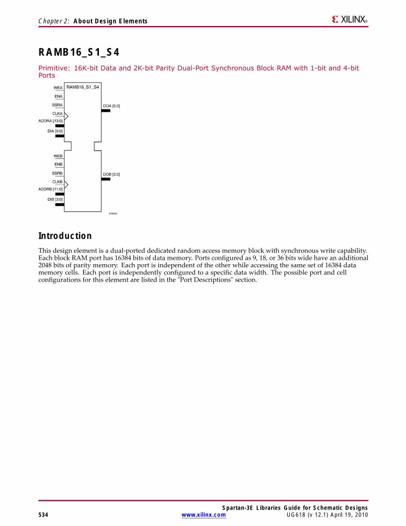
Chapter 2: About Design Elements
RAMB16_S1_S4Primitive: 16K-bit Data and 2K-bit Parity Dual-Port Synchronous Block RAM with 1-bit and 4-bitPorts
IntroductionThis design element is a dual-ported dedicated random access memory block with synchronous write capability.Each block RAM port has 16384 bits of data memory. Ports configured as 9, 18, or 36 bits wide have an additional2048 bits of parity memory. Each port is independent of the other while accessing the same set of 16384 datamemory cells. Each port is independently configured to a specific data width. The possible port and cellconfigurations for this element are listed in the "Port Descriptions" section.
Spartan-3E Libraries Guide for Schematic Designs534 www.xilinx.com UG618 (v 12.1) April 19, 2010
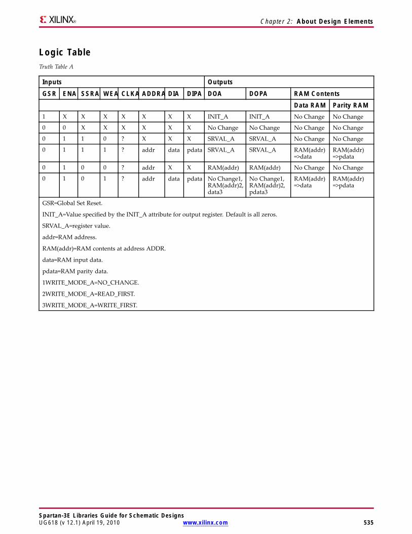
Chapter 2: About Design Elements
Logic TableTruth Table A
Inputs Outputs
GSR ENA SSRA WEA CLKA ADDRA DIA DIPA DOA DOPA RAM ContentsData RAM Parity RAM
1 X X X X X X X INIT_A INIT_A No Change No Change
0 0 X X X X X X No Change No Change No Change No Change
0 1 1 0 ? X X X SRVAL_A SRVAL_A No Change No Change
0 1 1 1 ? addr data pdata SRVAL_A SRVAL_A RAM(addr)=>data
RAM(addr)=>pdata
0 1 0 0 ? addr X X RAM(addr) RAM(addr) No Change No Change
0 1 0 1 ? addr data pdata No Change1,RAM(addr)2,data3
No Change1,RAM(addr)2,pdata3
RAM(addr)=>data
RAM(addr)=>pdata
GSR=Global Set Reset.
INIT_A=Value specified by the INIT_A attribute for output register. Default is all zeros.
SRVAL_A=register value.
addr=RAM address.
RAM(addr)=RAM contents at address ADDR.
data=RAM input data.
pdata=RAM parity data.
1WRITE_MODE_A=NO_CHANGE.
2WRITE_MODE_A=READ_FIRST.
3WRITE_MODE_A=WRITE_FIRST.
Spartan-3E Libraries Guide for Schematic DesignsUG618 (v 12.1) April 19, 2010 www.xilinx.com 535

Chapter 2: About Design Elements
Truth Table B
Inputs Outputs
GSR ENB SSRB WEB CLKB ADDRB DIB DIPB DOB DOPB RAM ContentsDataRAM
ParityRAM
1 X X X X X X X INIT_B INIT_B No Change No Change
0 0 X X X X X X No Change No Change No Change No Change
0 1 1 0 ? X X X SRVAL_B SRVAL_B No Change No Change
0 1 1 1 ? addr data pdata SRVAL_B SRVAL_B RAM(addr)=>data
RAM(addr)=>pdata
0 1 0 0 ? addr X X RAM(addr) RAM(addr) No Change No Change
0 1 0 1 ? addr data pdata No Change1,RAM(addr)=>data,data3
No Change1,RAM(addr)=>data,pdata3
RAM(addr)=>data
RAM(addr)=>pdata
GSR=Global Set Reset.
INIT_B=Value specified by the INIT_B attribute for output registers. Default is all zeros.
SRVAL_B=register value.
addr=RAM address.
RAM(addr)=RAM contents at address ADDR.
data=RAM input data.
pdata=RAM parity data.
1WRITE_MODE_B=NO_CHANGE.
2WRITE_MODE_B=READ_FIRST.
3WRITE_MODE_B=WRITE_FIRST.
Port DescriptionsPort A Port BDesignElement
DataCells(a)
ParityCells(a)
AddressBus
DataBus
ParityBus
DataCells(a)
ParityCells(a)
AddressBus
DataBus
ParityBus
RAMB16_S1_S4 16384 x1
- (13:0) (0:0) - 4096 x 4 - (11:0) (3:0) -
(a)Depth x Width
Each port is fully synchronous with independent clock pins. All Port A input pins have setup time referencedto the CLKA pin and its data output bus DOA has a clock-to-out time referenced to the CLKA. All Port Binput pins have setup time referenced to the CLKB pin and its data output bus DOB has a clock-to-out timereferenced to the CLKB. The enable ENA pin controls read, write, and reset for Port A. When ENA is Low, nodata is written and the outputs (DOA and DOPA) retain the last state. When ENA is High and reset (SSRA) isHigh, DOA and DOPA are set to SRVAL_A during the Low-to-High clock (CLKA) transition; if write enable(WEA) is High, the memory contents reflect the data at DIA and DIPA. When ENA is High and WEA is Low,the data stored in the RAM address (ADDRA) is read during the Low-to-High clock transition. By default,WRITE_MODE_A=WRITE_FIRST, when ENA and WEA are High, the data on the data inputs (DIA and DIPA) isloaded into the word selected by the write address (ADDRA) during the Low-to-High clock transition and thedata outputs (DOA and DOPA) reflect the selected (addressed) word.
Spartan-3E Libraries Guide for Schematic Designs536 www.xilinx.com UG618 (v 12.1) April 19, 2010
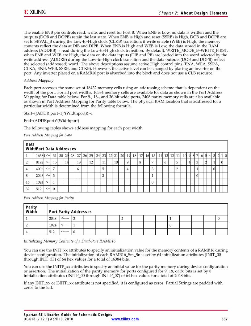
Chapter 2: About Design Elements
The enable ENB pin controls read, write, and reset for Port B. When ENB is Low, no data is written and theoutputs (DOB and DOPB) retain the last state. When ENB is High and reset (SSRB) is High, DOB and DOPB areset to SRVAL_B during the Low-to-High clock (CLKB) transition; if write enable (WEB) is High, the memorycontents reflect the data at DIB and DIPB. When ENB is High and WEB is Low, the data stored in the RAMaddress (ADDRB) is read during the Low-to-High clock transition. By default, WRITE_MODE_B=WRITE_FIRST,when ENB and WEB are High, the data on the data inputs (DIB and PB) are loaded into the word selected by thewrite address (ADDRB) during the Low-to-High clock transition and the data outputs (DOB and DOPB) reflectthe selected (addressed) word. The above descriptions assume active High control pins (ENA, WEA, SSRA,CLKA, ENB, WEB, SSRB, and CLKB). However, the active level can be changed by placing an inverter on theport. Any inverter placed on a RAMB16 port is absorbed into the block and does not use a CLB resource.
Address Mapping
Each port accesses the same set of 18432 memory cells using an addressing scheme that is dependent on thewidth of the port. For all port widths, 16384 memory cells are available for data as shown in the Port AddressMapping for Data table below. For 9-, 18-, and 36-bit wide ports, 2408 parity memory cells are also availableas shown in Port Address Mapping for Parity table below. The physical RAM location that is addressed for aparticular width is determined from the following formula.
Start=((ADDR port+1)*(Widthport)) -1
End=(ADDRport)*(Widthport)
The following tables shows address mapping for each port width.
Port Address Mapping for Data
DataWidthPort Data Addresses1 16384 <-- 31 30 29 28 27 26 25 24 23 22 21 20 19 18 17 16 15 14 13 12 11 10 9 8 7 6 5 4 3 2 1 0
2 8192 <-- 15 14 13 12 11 10 9 8 7 6 5 4 3 2 1 0
4 4096 <-- 7 6 5 4 3 2 1 0
8 2048 <-- 3 2 1 0
16 1024 <-- 1 0
32 512 <-- 0
Port Address Mapping for Parity
ParityWidth Port Parity Addresses1 2048 <----- 3 2 1 0
2 1024 <----- 1 0
4 512 <----- 0
Initializing Memory Contents of a Dual-Port RAMB16
You can use the INIT_xx attributes to specify an initialization value for the memory contents of a RAMB16 duringdevice configuration. The initialization of each RAMB16_Sm_Sn is set by 64 initialization attributes (INIT_00through INIT_3F) of 64 hex values for a total of 16384 bits.
You can use the INITP_xx attributes to specify an initial value for the parity memory during device configurationor assertion. The initialization of the parity memory for ports configured for 9, 18, or 36 bits is set by 8initialization attributes (INITP_00 through INITP_07) of 64 hex values for a total of 2048 bits.
If any INIT_xx or INITP_xx attribute is not specified, it is configured as zeros. Partial Strings are padded withzeros to the left.
Spartan-3E Libraries Guide for Schematic DesignsUG618 (v 12.1) April 19, 2010 www.xilinx.com 537

Chapter 2: About Design Elements
Initializing the Output Register of a Dual-Port RAMB16
In Spartan®-3A and above devices, each bit in an output register can be initialized at power on (when GSR ishigh) to either a 0 or 1. In addition, the initial state specified for power on can be different than the state thatresults from assertion of a set/reset. Four properties control initialization of the output register for a dual-portRAMB16: INIT_A, INIT_B, SRVAL_A, and SRVAL_B. The INIT_A attribute specifies the output register value atpower on for Port A and the INIT_B attribute specifies the value for Port B. You can use the SRVAL_A attribute todefine the state resulting from assertion of the SSR (set/reset) input on Port A. You can use the SRVAL_B attributeto define the state resulting from assertion of the SSR input on Port B.
The INIT_A, INIT_B, SRVAL_A, and SRVAL_B attributes specify the initialization value as a hexadecimal String.The value is dependent upon the port width. For example, for a RAMB16_S1_S4 with Port A width equal to 1and Port B width equal to 4, the Port A output register contains 1 bit and the Port B output register contains 4bits. Therefore, the INIT_A or SRVAL_A value can only be specified as a 1 or 0. For Port B, the output registercontains 4 bits. In this case, you can use INIT_B or SRVAL_B to specify a hexadecimal value from 0 through F toinitialize the 4 bits of the output register.
For those ports that include parity bits, the parity portion of the output register is specified in the high order bitposition of the INIT_A, INIT_B, SRVAL_A, or SRVAL_B value.
The INIT and SRVAL attributes default to zero if they are not set by you.
Write Mode Selection
TheWRITE_MODE_A attribute controls the memory and output contents of Port A for a dual-port RAMB16. TheWRITE_MODE_B attribute does the same for Port B. By default, both WRITE_MODE_A and WRITE_MODE_Bare set to WRITE_FIRST. This means that input is read, written to memory, and then passed to output. You canset the write mode for Port A and Port B to READ_FIRST to read the memory contents, pass the memory contentsto the outputs, and then write the input to memory. Or, you can set the write mode to NO_CHANGE to havethe input written to memory without changing the output. The Port A and Port B Conflict Resolution sectiondescribes how read/write conflicts are resolved when both Port A and Port B are attempting to read/write tothe same memory cells.
Port A and Port B Conflict Resolution
Spartan-3A block SelectRAM™ is True Dual-Port RAM that allows both ports to simultaneously access the samememory cell. When one port writes to a given memory cell, the other port must not address that memory cell (fora write or a read) within the clock-to-clock setup window.
The following tables summarize the collision detection behavior of the dual-port RAMB16 based on theWRITE_MODE_A and WRITE_MODE_B settings.
WRITE_MODE_A=NO_CHANGE and WRITE_MODE_B=NO_CHANGE
WEA WEB CLKA CLKB DIA DIB DIPA DIPB DOA DOB DOPA DOPBDataRAM
ParityRam
0 0 ? ? DIA DIB DIPA DIPB RAM RAM RAM RAM NoChange
NoChange
1 0 ? ? DIA DIB DIPA DIPB NoChange
X NoChange
X DIA DIPA
0 1 ? ? DIA DIB DIPA DIPB X NoChange
X NoChange
DIB DIPB
1 1 ? ? DIA DIB DIPA DIPB NoChange
NoChange
NoChange
NoChange
X X
Spartan-3E Libraries Guide for Schematic Designs538 www.xilinx.com UG618 (v 12.1) April 19, 2010
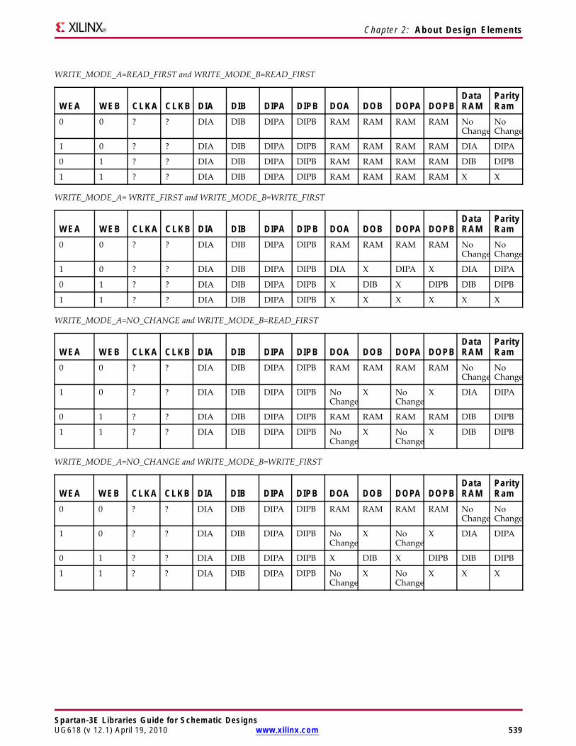
Chapter 2: About Design Elements
WRITE_MODE_A=READ_FIRST and WRITE_MODE_B=READ_FIRST
WEA WEB CLKA CLKB DIA DIB DIPA DIPB DOA DOB DOPA DOPBDataRAM
ParityRam
0 0 ? ? DIA DIB DIPA DIPB RAM RAM RAM RAM NoChange
NoChange
1 0 ? ? DIA DIB DIPA DIPB RAM RAM RAM RAM DIA DIPA
0 1 ? ? DIA DIB DIPA DIPB RAM RAM RAM RAM DIB DIPB
1 1 ? ? DIA DIB DIPA DIPB RAM RAM RAM RAM X X
WRITE_MODE_A= WRITE_FIRST and WRITE_MODE_B=WRITE_FIRST
WEA WEB CLKA CLKB DIA DIB DIPA DIPB DOA DOB DOPA DOPBDataRAM
ParityRam
0 0 ? ? DIA DIB DIPA DIPB RAM RAM RAM RAM NoChange
NoChange
1 0 ? ? DIA DIB DIPA DIPB DIA X DIPA X DIA DIPA
0 1 ? ? DIA DIB DIPA DIPB X DIB X DIPB DIB DIPB
1 1 ? ? DIA DIB DIPA DIPB X X X X X X
WRITE_MODE_A=NO_CHANGE and WRITE_MODE_B=READ_FIRST
WEA WEB CLKA CLKB DIA DIB DIPA DIPB DOA DOB DOPA DOPBDataRAM
ParityRam
0 0 ? ? DIA DIB DIPA DIPB RAM RAM RAM RAM NoChange
NoChange
1 0 ? ? DIA DIB DIPA DIPB NoChange
X NoChange
X DIA DIPA
0 1 ? ? DIA DIB DIPA DIPB RAM RAM RAM RAM DIB DIPB
1 1 ? ? DIA DIB DIPA DIPB NoChange
X NoChange
X DIB DIPB
WRITE_MODE_A=NO_CHANGE and WRITE_MODE_B=WRITE_FIRST
WEA WEB CLKA CLKB DIA DIB DIPA DIPB DOA DOB DOPA DOPBDataRAM
ParityRam
0 0 ? ? DIA DIB DIPA DIPB RAM RAM RAM RAM NoChange
NoChange
1 0 ? ? DIA DIB DIPA DIPB NoChange
X NoChange
X DIA DIPA
0 1 ? ? DIA DIB DIPA DIPB X DIB X DIPB DIB DIPB
1 1 ? ? DIA DIB DIPA DIPB NoChange
X NoChange
X X X
Spartan-3E Libraries Guide for Schematic DesignsUG618 (v 12.1) April 19, 2010 www.xilinx.com 539
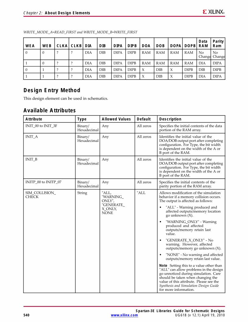
Chapter 2: About Design Elements
WRITE_MODE_A=READ_FIRST and WRITE_MODE_B=WRITE_FIRST
WEA WEB CLKA CLKB DIA DIB DIPA DIPB DOA DOB DOPA DOPBDataRAM
ParityRam
0 0 ? ? DIA DIB DIPA DIPB RAM RAM RAM RAM NoChange
NoChange
1 0 ? ? DIA DIB DIPA DIPB RAM RAM RAM RAM DIA DIPA
0 1 ? ? DIA DIB DIPA DIPB X DIB X DIPB DIB DIPB
1 1 ? ? DIA DIB DIPA DIPB X DIB X DIPB DIA DIPA
Design Entry MethodThis design element can be used in schematics.
Available AttributesAttribute Type Allowed Values Default DescriptionINIT_00 to INIT_3F Binary/
HexadecimalAny All zeros Specifies the initial contents of the data
portion of the RAM array.
INIT_A Binary/Hexadecimal
Any All zeros Identifies the initial value of theDOA/DOB output port after completingconfiguration. For Type, the bit widthis dependent on the width of the A orB port of the RAM.
INIT_B Binary/Hexadecimal
Any All zeros Identifies the initial value of theDOA/DOB output port after completingconfiguration. For Type, the bit widthis dependent on the width of the A orB port of the RAM.
INITP_00 to INITP_07 Binary/Hexadecimal
Any All zeros Specifies the initial contents of theparity portion of the RAM array.
SIM_COLLISION_CHECK
String "ALL,"WARNING_ONLY","GENERATE_X_ONLY,NONE
"ALL Allows modification of the simulationbehavior if a memory collision occurs.The output is affected as follows:
• "ALL" - Warning produced andaffected outputs/memory locationgo unknown (X).
• "WARNING_ONLY" - Warningproduced and affectedoutputs/memory retain lastvalue.
• "GENERATE_X_ONLY" - Nowarning. However, affectedoutputs/memory go unknown (X).
• "NONE" - No warning and affectedoutputs/memory retain last value.
Note Setting this to a value other than"ALL" can allow problems in the designgo unnoticed during simulation. Careshould be taken when changing thevalue of this attribute. Please see theSynthesis and Simulation Design Guidefor more information.
Spartan-3E Libraries Guide for Schematic Designs540 www.xilinx.com UG618 (v 12.1) April 19, 2010
Chapter 2: About Design Elements
Attribute Type Allowed Values Default DescriptionSRVAL_A Binary/
HexadecimalAny All zeros Allows the individual selection of
whether the DOA/DOB output portsets (go to a one) or reset (go to a zero)upon the assertion of the RSTA pin. ForType, the bit width is dependent on thewidth of the A port of the RAM.
SRVAL_B Binary/Hexadecimal
Any All zeros Allows the individual selection ofwhether the DOA/DOB output portsets (go to a one) or reset (go to a zero)upon the assertion of the RSTB pin. ForType, the bit width is dependent on thewidth of the B port of the RAM.
WRITE_MODE_A String "WRITE_FIRST","READ_FIRST","NO_CHANGE
"WRITE_FIRST
Specifies the behavior of the DOA/DOBport upon a write command tothe respected port. If set to"WRITE_FIRST", the same portthat is written to displays the contentsof the written data to the outputsupon completion of the operation."READ_FIRST" displays the priorcontents of the RAM to the outputport prior to writing the new data."NO_CHANGE" keeps the previousvalue on the output port and wontupdate the output port upon a writecommand. This is the suggested modeif not using the read data from aparticular port of the RAM
WRITE_MODE_B String "WRITE_FIRST","READ_FIRST","NO_CHANGE
"WRITE_FIRST
Specifies the behavior of the DOA/DOBport upon a write command tothe respected port. If set to"WRITE_FIRST", the same portthat is written to displays the contentsof the written data to the outputsupon completion of the operation."READ_FIRST" displays the priorcontents of the RAM to the outputport prior to writing the new data."NO_CHANGE" keeps the previousvalue on the output port and wontupdate the output port upon a writecommand. This is the suggested modeif not using the read data from aparticular port of the RAM.
For More Information• See the Spartan-3 Generation FPGA User Guide.
• See the Spartan-3E FPGA Family Complete Data Sheet.
Spartan-3E Libraries Guide for Schematic DesignsUG618 (v 12.1) April 19, 2010 www.xilinx.com 541

Spartan-3E Libraries Guide for Schematic Designs542 www.xilinx.com UG618 (v 12.1) April 19, 2010
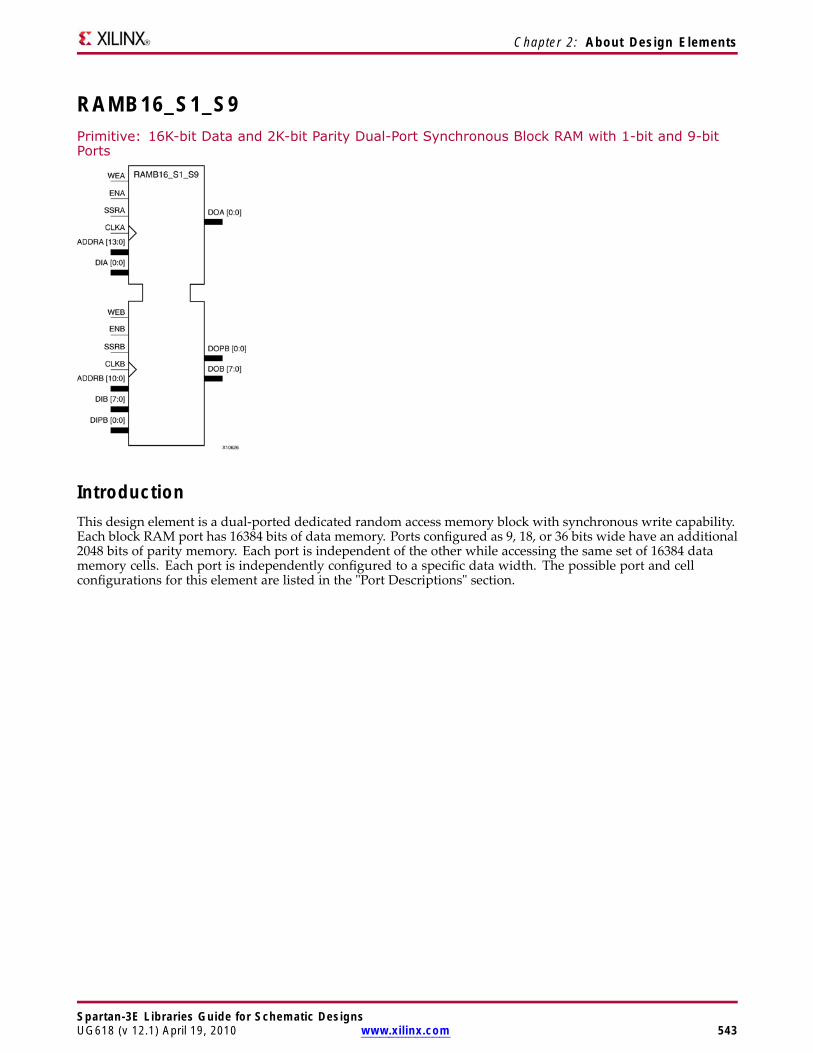
Chapter 2: About Design Elements
RAMB16_S1_S9Primitive: 16K-bit Data and 2K-bit Parity Dual-Port Synchronous Block RAM with 1-bit and 9-bitPorts
IntroductionThis design element is a dual-ported dedicated random access memory block with synchronous write capability.Each block RAM port has 16384 bits of data memory. Ports configured as 9, 18, or 36 bits wide have an additional2048 bits of parity memory. Each port is independent of the other while accessing the same set of 16384 datamemory cells. Each port is independently configured to a specific data width. The possible port and cellconfigurations for this element are listed in the "Port Descriptions" section.
Spartan-3E Libraries Guide for Schematic DesignsUG618 (v 12.1) April 19, 2010 www.xilinx.com 543

Chapter 2: About Design Elements
Logic TableTruth Table A
Inputs Outputs
GSR ENA SSRA WEA CLKA ADDRA DIA DIPA DOA DOPA RAM ContentsData RAM Parity RAM
1 X X X X X X X INIT_A INIT_A No Change No Change
0 0 X X X X X X No Change No Change No Change No Change
0 1 1 0 ? X X X SRVAL_A SRVAL_A No Change No Change
0 1 1 1 ? addr data pdata SRVAL_A SRVAL_A RAM(addr)=>data
RAM(addr)=>pdata
0 1 0 0 ? addr X X RAM(addr) RAM(addr) No Change No Change
0 1 0 1 ? addr data pdata No Change1,RAM(addr)2,data3
No Change1,RAM(addr)2,pdata3
RAM(addr)=>data
RAM(addr)=>pdata
GSR=Global Set Reset.
INIT_A=Value specified by the INIT_A attribute for output register. Default is all zeros.
SRVAL_A=register value.
addr=RAM address.
RAM(addr)=RAM contents at address ADDR.
data=RAM input data.
pdata=RAM parity data.
1WRITE_MODE_A=NO_CHANGE.
2WRITE_MODE_A=READ_FIRST.
3WRITE_MODE_A=WRITE_FIRST.
Spartan-3E Libraries Guide for Schematic Designs544 www.xilinx.com UG618 (v 12.1) April 19, 2010

Chapter 2: About Design Elements
Truth Table B
Inputs Outputs
GSR ENB SSRB WEB CLKB ADDRB DIB DIPB DOB DOPB RAM ContentsDataRAM
ParityRAM
1 X X X X X X X INIT_B INIT_B No Change No Change
0 0 X X X X X X No Change No Change No Change No Change
0 1 1 0 ? X X X SRVAL_B SRVAL_B No Change No Change
0 1 1 1 ? addr data pdata SRVAL_B SRVAL_B RAM(addr)=>data
RAM(addr)=>pdata
0 1 0 0 ? addr X X RAM(addr) RAM(addr) No Change No Change
0 1 0 1 ? addr data pdata No Change1,RAM(addr)=>data,data3
No Change1,RAM(addr)=>data,pdata3
RAM(addr)=>data
RAM(addr)=>pdata
GSR=Global Set Reset.
INIT_B=Value specified by the INIT_B attribute for output registers. Default is all zeros.
SRVAL_B=register value.
addr=RAM address.
RAM(addr)=RAM contents at address ADDR.
data=RAM input data.
pdata=RAM parity data.
1WRITE_MODE_B=NO_CHANGE.
2WRITE_MODE_B=READ_FIRST.
3WRITE_MODE_B=WRITE_FIRST.
Port DescriptionsPort A Port BDesignElement
DataCells(a)
ParityCells(a)
AddressBus
DataBus
ParityBus
DataCells(a)
ParityCells(a)
AddressBus
DataBus
ParityBus
RAMB16_S1_S9 16384 x1
- (13:0) (0:0) - 2048 x 8 2048 x 1 (10:0) (7:0) (0:0)
(a) Depth x Width
Each port is fully synchronous with independent clock pins. All Port A input pins have setup time referencedto the CLKA pin and its data output bus DOA has a clock-to-out time referenced to the CLKA. All Port Binput pins have setup time referenced to the CLKB pin and its data output bus DOB has a clock-to-out timereferenced to the CLKB. The enable ENA pin controls read, write, and reset for Port A. When ENA is Low, nodata is written and the outputs (DOA and DOPA) retain the last state. When ENA is High and reset (SSRA) isHigh, DOA and DOPA are set to SRVAL_A during the Low-to-High clock (CLKA) transition; if write enable(WEA) is High, the memory contents reflect the data at DIA and DIPA. When ENA is High and WEA is Low,the data stored in the RAM address (ADDRA) is read during the Low-to-High clock transition. By default,WRITE_MODE_A=WRITE_FIRST, when ENA and WEA are High, the data on the data inputs (DIA and DIPA) isloaded into the word selected by the write address (ADDRA) during the Low-to-High clock transition and thedata outputs (DOA and DOPA) reflect the selected (addressed) word.
Spartan-3E Libraries Guide for Schematic DesignsUG618 (v 12.1) April 19, 2010 www.xilinx.com 545
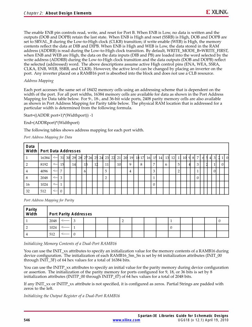
Chapter 2: About Design Elements
The enable ENB pin controls read, write, and reset for Port B. When ENB is Low, no data is written and theoutputs (DOB and DOPB) retain the last state. When ENB is High and reset (SSRB) is High, DOB and DOPB areset to SRVAL_B during the Low-to-High clock (CLKB) transition; if write enable (WEB) is High, the memorycontents reflect the data at DIB and DIPB. When ENB is High and WEB is Low, the data stored in the RAMaddress (ADDRB) is read during the Low-to-High clock transition. By default, WRITE_MODE_B=WRITE_FIRST,when ENB and WEB are High, the data on the data inputs (DIB and PB) are loaded into the word selected by thewrite address (ADDRB) during the Low-to-High clock transition and the data outputs (DOB and DOPB) reflectthe selected (addressed) word. The above descriptions assume active High control pins (ENA, WEA, SSRA,CLKA, ENB, WEB, SSRB, and CLKB). However, the active level can be changed by placing an inverter on theport. Any inverter placed on a RAMB16 port is absorbed into the block and does not use a CLB resource.
Address Mapping
Each port accesses the same set of 18432 memory cells using an addressing scheme that is dependent on thewidth of the port. For all port widths, 16384 memory cells are available for data as shown in the Port AddressMapping for Data table below. For 9-, 18-, and 36-bit wide ports, 2408 parity memory cells are also availableas shown in Port Address Mapping for Parity table below. The physical RAM location that is addressed for aparticular width is determined from the following formula.
Start=((ADDR port+1)*(Widthport)) -1
End=(ADDRport)*(Widthport)
The following tables shows address mapping for each port width.
Port Address Mapping for Data
DataWidth Port Data Addresses1 16384 <-- 31 30 29 28 27 26 25 24 23 22 21 20 19 18 17 16 15 14 13 12 11 10 9 8 7 6 5 4 3 2 1 0
2 8192 <-- 15 14 13 12 11 10 9 8 7 6 5 4 3 2 1 0
4 4096 <-- 7 6 5 4 3 2 1 0
8 2048 <-- 3 2 1 0
16 1024 <-- 1 0
32 512 <-- 0
Port Address Mapping for Parity
ParityWidth Port Parity Addresses1 2048 <----- 3 2 1 0
2 1024 <----- 1 0
4 512 <----- 0
Initializing Memory Contents of a Dual-Port RAMB16
You can use the INIT_xx attributes to specify an initialization value for the memory contents of a RAMB16 duringdevice configuration. The initialization of each RAMB16_Sm_Sn is set by 64 initialization attributes (INIT_00through INIT_3F) of 64 hex values for a total of 16384 bits.
You can use the INITP_xx attributes to specify an initial value for the parity memory during device configurationor assertion. The initialization of the parity memory for ports configured for 9, 18, or 36 bits is set by 8initialization attributes (INITP_00 through INITP_07) of 64 hex values for a total of 2048 bits.
If any INIT_xx or INITP_xx attribute is not specified, it is configured as zeros. Partial Strings are padded withzeros to the left.
Initializing the Output Register of a Dual-Port RAMB16
Spartan-3E Libraries Guide for Schematic Designs546 www.xilinx.com UG618 (v 12.1) April 19, 2010
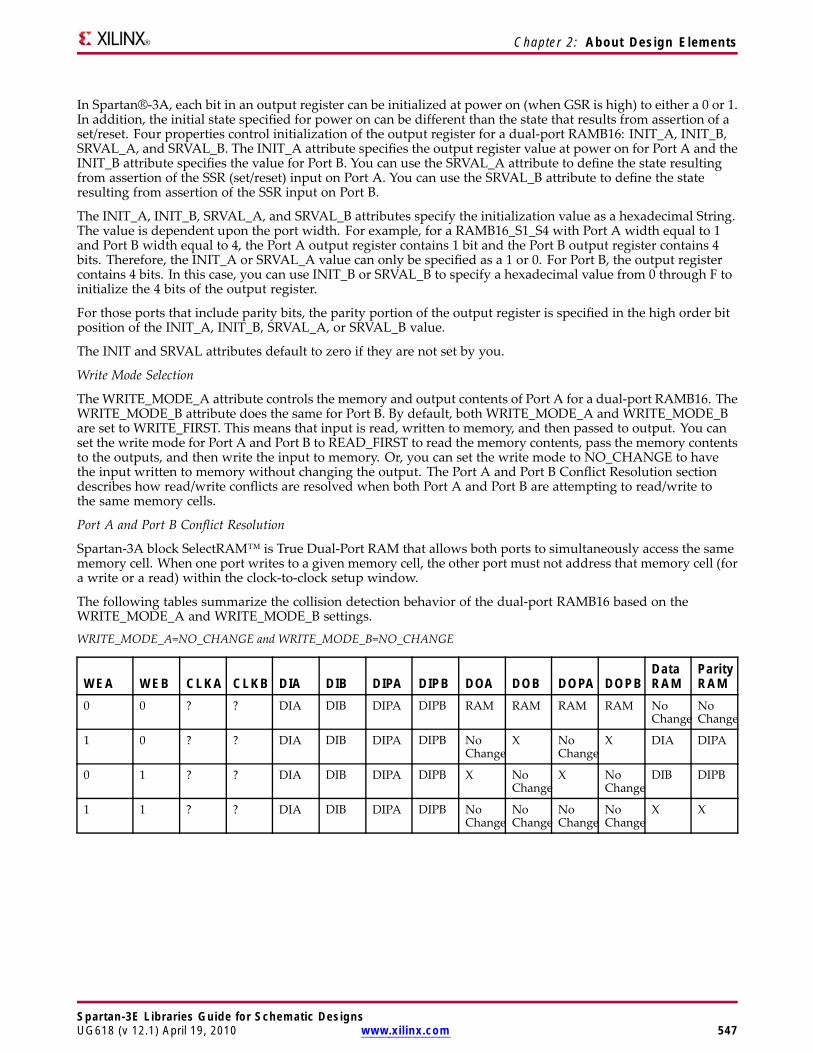
Chapter 2: About Design Elements
In Spartan®-3A, each bit in an output register can be initialized at power on (when GSR is high) to either a 0 or 1.In addition, the initial state specified for power on can be different than the state that results from assertion of aset/reset. Four properties control initialization of the output register for a dual-port RAMB16: INIT_A, INIT_B,SRVAL_A, and SRVAL_B. The INIT_A attribute specifies the output register value at power on for Port A and theINIT_B attribute specifies the value for Port B. You can use the SRVAL_A attribute to define the state resultingfrom assertion of the SSR (set/reset) input on Port A. You can use the SRVAL_B attribute to define the stateresulting from assertion of the SSR input on Port B.
The INIT_A, INIT_B, SRVAL_A, and SRVAL_B attributes specify the initialization value as a hexadecimal String.The value is dependent upon the port width. For example, for a RAMB16_S1_S4 with Port A width equal to 1and Port B width equal to 4, the Port A output register contains 1 bit and the Port B output register contains 4bits. Therefore, the INIT_A or SRVAL_A value can only be specified as a 1 or 0. For Port B, the output registercontains 4 bits. In this case, you can use INIT_B or SRVAL_B to specify a hexadecimal value from 0 through F toinitialize the 4 bits of the output register.
For those ports that include parity bits, the parity portion of the output register is specified in the high order bitposition of the INIT_A, INIT_B, SRVAL_A, or SRVAL_B value.
The INIT and SRVAL attributes default to zero if they are not set by you.
Write Mode Selection
TheWRITE_MODE_A attribute controls the memory and output contents of Port A for a dual-port RAMB16. TheWRITE_MODE_B attribute does the same for Port B. By default, both WRITE_MODE_A and WRITE_MODE_Bare set to WRITE_FIRST. This means that input is read, written to memory, and then passed to output. You canset the write mode for Port A and Port B to READ_FIRST to read the memory contents, pass the memory contentsto the outputs, and then write the input to memory. Or, you can set the write mode to NO_CHANGE to havethe input written to memory without changing the output. The Port A and Port B Conflict Resolution sectiondescribes how read/write conflicts are resolved when both Port A and Port B are attempting to read/write tothe same memory cells.
Port A and Port B Conflict Resolution
Spartan-3A block SelectRAM™ is True Dual-Port RAM that allows both ports to simultaneously access the samememory cell. When one port writes to a given memory cell, the other port must not address that memory cell (fora write or a read) within the clock-to-clock setup window.
The following tables summarize the collision detection behavior of the dual-port RAMB16 based on theWRITE_MODE_A and WRITE_MODE_B settings.
WRITE_MODE_A=NO_CHANGE and WRITE_MODE_B=NO_CHANGE
WEA WEB CLKA CLKB DIA DIB DIPA DIPB DOA DOB DOPA DOPBDataRAM
ParityRAM
0 0 ? ? DIA DIB DIPA DIPB RAM RAM RAM RAM NoChange
NoChange
1 0 ? ? DIA DIB DIPA DIPB NoChange
X NoChange
X DIA DIPA
0 1 ? ? DIA DIB DIPA DIPB X NoChange
X NoChange
DIB DIPB
1 1 ? ? DIA DIB DIPA DIPB NoChange
NoChange
NoChange
NoChange
X X
Spartan-3E Libraries Guide for Schematic DesignsUG618 (v 12.1) April 19, 2010 www.xilinx.com 547
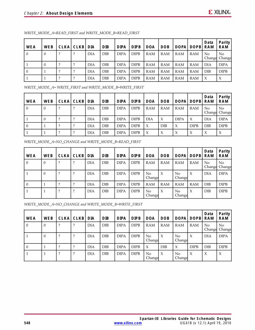
Chapter 2: About Design Elements
WRITE_MODE_A=READ_FIRST and WRITE_MODE_B=READ_FIRST
WEA WEB CLKA CLKB DIA DIB DIPA DIPB DOA DOB DOPA DOPBDataRAM
ParityRAM
0 0 ? ? DIA DIB DIPA DIPB RAM RAM RAM RAM NoChange
NoChange
1 0 ? ? DIA DIB DIPA DIPB RAM RAM RAM RAM DIA DIPA
0 1 ? ? DIA DIB DIPA DIPB RAM RAM RAM RAM DIB DIPB
1 1 ? ? DIA DIB DIPA DIPB RAM RAM RAM RAM X X
WRITE_MODE_A= WRITE_FIRST and WRITE_MODE_B=WRITE_FIRST
WEA WEB CLKA CLKB DIA DIB DIPA DIPB DOA DOB DOPA DOPBDataRAM
ParityRAM
0 0 ? ? DIA DIB DIPA DIPB RAM RAM RAM RAM NoChange
NoChange
1 0 ? ? DIA DIB DIPA DIPB DIA X DIPA X DIA DIPA
0 1 ? ? DIA DIB DIPA DIPB X DIB X DIPB DIB DIPB
1 1 ? ? DIA DIB DIPA DIPB X X X X X X
WRITE_MODE_A=NO_CHANGE and WRITE_MODE_B=READ_FIRST
WEA WEB CLKA CLKB DIA DIB DIPA DIPB DOA DOB DOPA DOPBDataRAM
ParityRAM
0 0 ? ? DIA DIB DIPA DIPB RAM RAM RAM RAM NoChange
NoChange
1 0 ? ? DIA DIB DIPA DIPB NoChange
X NoChange
X DIA DIPA
0 1 ? ? DIA DIB DIPA DIPB RAM RAM RAM RAM DIB DIPB
1 1 ? ? DIA DIB DIPA DIPB NoChange
X NoChange
X DIB DIPB
WRITE_MODE_A=NO_CHANGE and WRITE_MODE_B=WRITE_FIRST
WEA WEB CLKA CLKB DIA DIB DIPA DIPB DOA DOB DOPA DOPBDataRAM
ParityRAM
0 0 ? ? DIA DIB DIPA DIPB RAM RAM RAM RAM NoChange
NoChange
1 0 ? ? DIA DIB DIPA DIPB NoChange
X NoChange
X DIA DIPA
0 1 ? ? DIA DIB DIPA DIPB X DIB X DIPB DIB DIPB
1 1 ? ? DIA DIB DIPA DIPB NoChange
X NoChange
X X X
Spartan-3E Libraries Guide for Schematic Designs548 www.xilinx.com UG618 (v 12.1) April 19, 2010
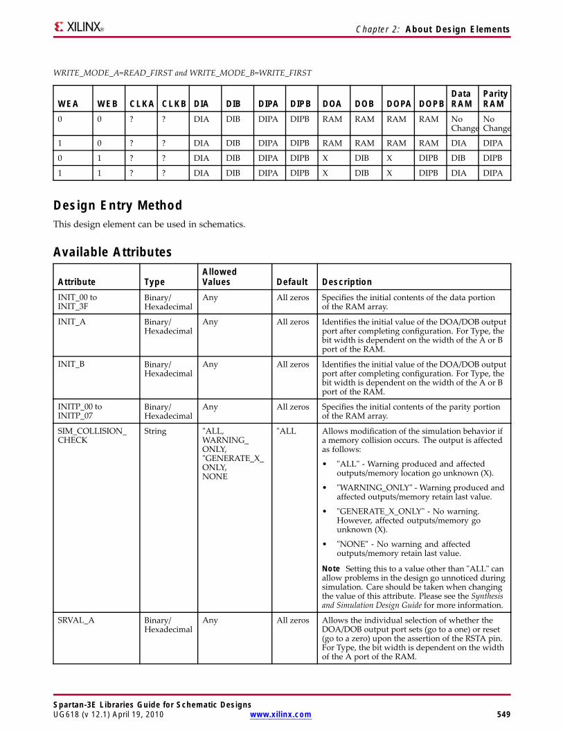
Chapter 2: About Design Elements
WRITE_MODE_A=READ_FIRST and WRITE_MODE_B=WRITE_FIRST
WEA WEB CLKA CLKB DIA DIB DIPA DIPB DOA DOB DOPA DOPBDataRAM
ParityRAM
0 0 ? ? DIA DIB DIPA DIPB RAM RAM RAM RAM NoChange
NoChange
1 0 ? ? DIA DIB DIPA DIPB RAM RAM RAM RAM DIA DIPA
0 1 ? ? DIA DIB DIPA DIPB X DIB X DIPB DIB DIPB
1 1 ? ? DIA DIB DIPA DIPB X DIB X DIPB DIA DIPA
Design Entry MethodThis design element can be used in schematics.
Available Attributes
Attribute TypeAllowedValues Default Description
INIT_00 toINIT_3F
Binary/Hexadecimal
Any All zeros Specifies the initial contents of the data portionof the RAM array.
INIT_A Binary/Hexadecimal
Any All zeros Identifies the initial value of the DOA/DOB outputport after completing configuration. For Type, thebit width is dependent on the width of the A or Bport of the RAM.
INIT_B Binary/Hexadecimal
Any All zeros Identifies the initial value of the DOA/DOB outputport after completing configuration. For Type, thebit width is dependent on the width of the A or Bport of the RAM.
INITP_00 toINITP_07
Binary/Hexadecimal
Any All zeros Specifies the initial contents of the parity portionof the RAM array.
SIM_COLLISION_CHECK
String "ALL,WARNING_ONLY,"GENERATE_X_ONLY,NONE
"ALL Allows modification of the simulation behavior ifa memory collision occurs. The output is affectedas follows:
• "ALL" - Warning produced and affectedoutputs/memory location go unknown (X).
• "WARNING_ONLY" - Warning produced andaffected outputs/memory retain last value.
• "GENERATE_X_ONLY" - No warning.However, affected outputs/memory gounknown (X).
• "NONE" - No warning and affectedoutputs/memory retain last value.
Note Setting this to a value other than "ALL" canallow problems in the design go unnoticed duringsimulation. Care should be taken when changingthe value of this attribute. Please see the Synthesisand Simulation Design Guide for more information.
SRVAL_A Binary/Hexadecimal
Any All zeros Allows the individual selection of whether theDOA/DOB output port sets (go to a one) or reset(go to a zero) upon the assertion of the RSTA pin.For Type, the bit width is dependent on the widthof the A port of the RAM.
Spartan-3E Libraries Guide for Schematic DesignsUG618 (v 12.1) April 19, 2010 www.xilinx.com 549

Chapter 2: About Design Elements
Attribute TypeAllowedValues Default Description
SRVAL_B Binary/Hexadecimal
Any All zeros Allows the individual selection of whether theDOA/DOB output port sets (go to a one) or reset(go to a zero) upon the assertion of the RSTB pin.For Type, the bit width is dependent on the widthof the B port of the RAM.
WRITE_MODE_A String "WRITE_FIRST","READ_FIRST","NO_CHANGE
"WRITE_FIRST
Specifies the behavior of the DOA/DOB port upona write command to the respected port. If set to"WRITE_FIRST", the same port that is writtento displays the contents of the written data tothe outputs upon completion of the operation."READ_FIRST" displays the prior contents of theRAM to the output port prior to writing the newdata. "NO_CHANGE" keeps the previous valueon the output port and wont update the outputport upon a write command. This is the suggestedmode if not using the read data from a particularport of the RAM.
WRITE_MODE_B String "WRITE_FIRST","READ_FIRST","NO_CHANGE
"WRITE_FIRST
Specifies the behavior of the DOA/DOB port upona write command to the respected port. If set to"WRITE_FIRST", the same port that is writtento displays the contents of the written data tothe outputs upon completion of the operation."READ_FIRST" displays the prior contents of theRAM to the output port prior to writing the newdata. "NO_CHANGE" keeps the previous valueon the output port and wont update the outputport upon a write command. This is the suggestedmode if not using the read data from a particularport of the RAM.
For More Information• See the Spartan-3 Generation FPGA User Guide.
• See the Spartan-3E FPGA Family Complete Data Sheet.
Spartan-3E Libraries Guide for Schematic Designs550 www.xilinx.com UG618 (v 12.1) April 19, 2010
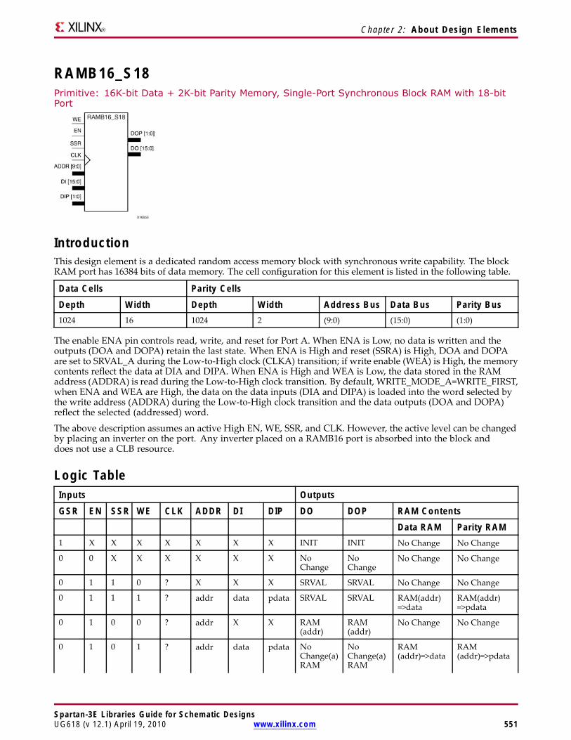
Chapter 2: About Design Elements
RAMB16_S18Primitive: 16K-bit Data + 2K-bit Parity Memory, Single-Port Synchronous Block RAM with 18-bitPort
IntroductionThis design element is a dedicated random access memory block with synchronous write capability. The blockRAM port has 16384 bits of data memory. The cell configuration for this element is listed in the following table.
Data Cells Parity CellsDepth Width Depth Width Address Bus Data Bus Parity Bus1024 16 1024 2 (9:0) (15:0) (1:0)
The enable ENA pin controls read, write, and reset for Port A. When ENA is Low, no data is written and theoutputs (DOA and DOPA) retain the last state. When ENA is High and reset (SSRA) is High, DOA and DOPAare set to SRVAL_A during the Low-to-High clock (CLKA) transition; if write enable (WEA) is High, the memorycontents reflect the data at DIA and DIPA. When ENA is High and WEA is Low, the data stored in the RAMaddress (ADDRA) is read during the Low-to-High clock transition. By default, WRITE_MODE_A=WRITE_FIRST,when ENA and WEA are High, the data on the data inputs (DIA and DIPA) is loaded into the word selected bythe write address (ADDRA) during the Low-to-High clock transition and the data outputs (DOA and DOPA)reflect the selected (addressed) word.
The above description assumes an active High EN, WE, SSR, and CLK. However, the active level can be changedby placing an inverter on the port. Any inverter placed on a RAMB16 port is absorbed into the block anddoes not use a CLB resource.
Logic TableInputs Outputs
GSR EN SSR WE CLK ADDR DI DIP DO DOP RAM ContentsData RAM Parity RAM
1 X X X X X X X INIT INIT No Change No Change
0 0 X X X X X X NoChange
NoChange
No Change No Change
0 1 1 0 ? X X X SRVAL SRVAL No Change No Change
0 1 1 1 ? addr data pdata SRVAL SRVAL RAM(addr)=>data
RAM(addr)=>pdata
0 1 0 0 ? addr X X RAM(addr)
RAM(addr)
No Change No Change
0 1 0 1 ? addr data pdata NoChange(a)RAM
NoChange(a)RAM
RAM(addr)=>data
RAM(addr)=>pdata
Spartan-3E Libraries Guide for Schematic DesignsUG618 (v 12.1) April 19, 2010 www.xilinx.com 551
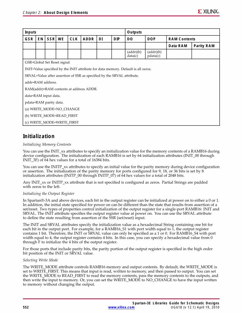
Chapter 2: About Design Elements
Inputs Outputs
GSR EN SSR WE CLK ADDR DI DIP DO DOP RAM ContentsData RAM Parity RAM
(addr)(b)data(c)
(addr)(b)pdata(c)
GSR=Global Set Reset signal
INIT=Value specified by the INIT attribute for data memory. Default is all zeros.
SRVAL=Value after assertion of SSR as specified by the SRVAL attribute.
addr=RAM address.
RAM(addr)=RAM contents at address ADDR.
data=RAM input data.
pdata=RAM parity data.
(a) WRITE_MODE=NO_CHANGE
(b) WRITE_MODE=READ_FIRST
(c) WRITE_MODE=WRITE_FIRST
InitializationInitializing Memory Contents
You can use the INIT_xx attributes to specify an initialization value for the memory contents of a RAMB16 duringdevice configuration. The initialization of each RAMB16 is set by 64 initialization attributes (INIT_00 throughINIT_3F) of 64 hex values for a total of 16384 bits.
You can use the INITP_xx attributes to specify an initial value for the parity memory during device configurationor assertion. The initialization of the parity memory for ports configured for 9, 18, or 36 bits is set by 8initialization attributes (INITP_00 through INITP_07) of 64 hex values for a total of 2048 bits.
Any INIT_xx or INITP_xx attribute that is not specified is configured as zeros. Partial Strings are paddedwith zeros to the left.
Initializing the Output Register
In Spartan®-3A and above devices, each bit in the output register can be initialized at power on to either a 0 or 1.In addition, the initial state specified for power on can be different than the state that results from assertion of aset/reset. Two types of properties control initialization of the output register for a single-port RAMB16: INIT andSRVAL. The INIT attribute specifies the output register value at power on. You can use the SRVAL attributeto define the state resulting from assertion of the SSR (set/reset) input.
The INIT and SRVAL attributes specify the initialization value as a hexadecimal String containing one bit foreach bit in the output port. For example, for a RAMB16_S1 with port width equal to 1, the output registercontains 1 bit. Therefore, the INIT or SRVAL value can only be specified as a 1 or 0. For RAMB16_S4 with portwidth equal to 4, the output register contains 4 bits. In this case, you can specify a hexadecimal value from 0through F to initialize the 4 bits of the output register.
For those ports that include parity bits, the parity portion of the output register is specified in the high orderbit position of the INIT or SRVAL value.
Selecting Write Mode
The WRITE_MODE attribute controls RAMB16 memory and output contents. By default, the WRITE_MODE isset to WRITE_FIRST. This means that input is read, written to memory, and then passed to output. You can setthe WRITE_MODE to READ_FIRST to read the memory contents, pass the memory contents to the outputs, andthen write the input to memory. Or, you can set the WRITE_MODE to NO_CHANGE to have the input writtento memory without changing the output.
Spartan-3E Libraries Guide for Schematic Designs552 www.xilinx.com UG618 (v 12.1) April 19, 2010
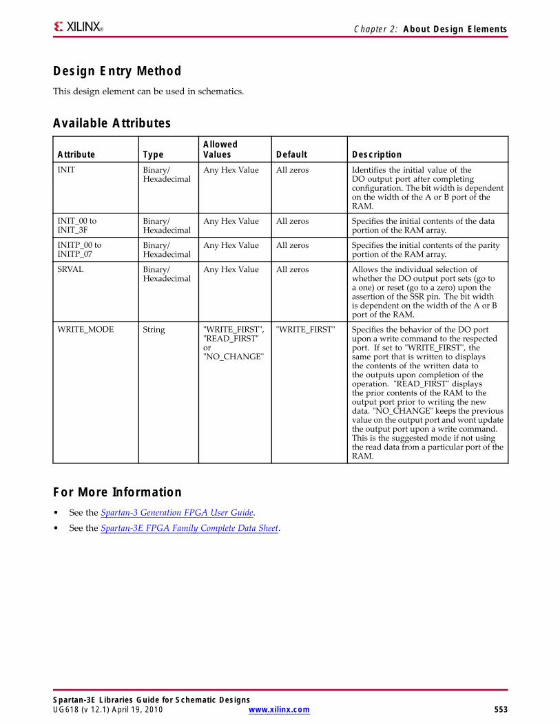
Chapter 2: About Design Elements
Design Entry MethodThis design element can be used in schematics.
Available Attributes
Attribute TypeAllowedValues Default Description
INIT Binary/Hexadecimal
Any Hex Value All zeros Identifies the initial value of theDO output port after completingconfiguration. The bit width is dependenton the width of the A or B port of theRAM.
INIT_00 toINIT_3F
Binary/Hexadecimal
Any Hex Value All zeros Specifies the initial contents of the dataportion of the RAM array.
INITP_00 toINITP_07
Binary/Hexadecimal
Any Hex Value All zeros Specifies the initial contents of the parityportion of the RAM array.
SRVAL Binary/Hexadecimal
Any Hex Value All zeros Allows the individual selection ofwhether the DO output port sets (go toa one) or reset (go to a zero) upon theassertion of the SSR pin. The bit widthis dependent on the width of the A or Bport of the RAM.
WRITE_MODE String "WRITE_FIRST","READ_FIRST"or"NO_CHANGE"
"WRITE_FIRST" Specifies the behavior of the DO portupon a write command to the respectedport. If set to "WRITE_FIRST", thesame port that is written to displaysthe contents of the written data tothe outputs upon completion of theoperation. "READ_FIRST" displaysthe prior contents of the RAM to theoutput port prior to writing the newdata. "NO_CHANGE" keeps the previousvalue on the output port and wont updatethe output port upon a write command.This is the suggested mode if not usingthe read data from a particular port of theRAM.
For More Information• See the Spartan-3 Generation FPGA User Guide.
• See the Spartan-3E FPGA Family Complete Data Sheet.
Spartan-3E Libraries Guide for Schematic DesignsUG618 (v 12.1) April 19, 2010 www.xilinx.com 553
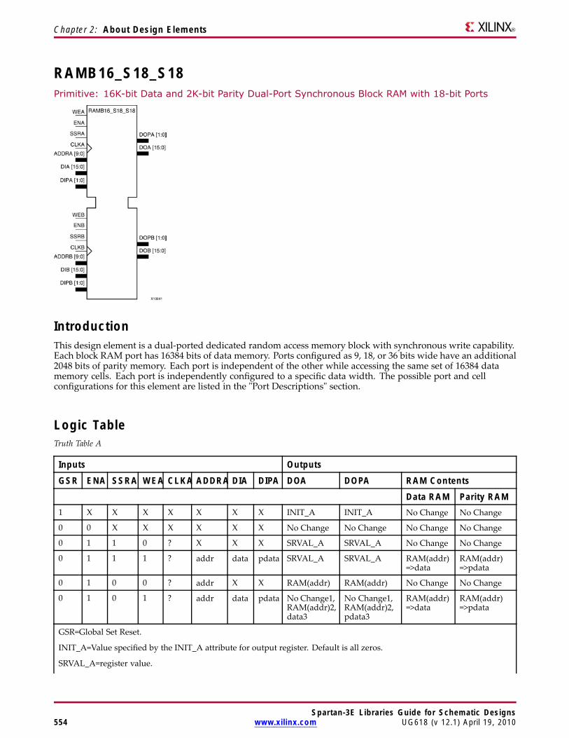
Chapter 2: About Design Elements
RAMB16_S18_S18Primitive: 16K-bit Data and 2K-bit Parity Dual-Port Synchronous Block RAM with 18-bit Ports
IntroductionThis design element is a dual-ported dedicated random access memory block with synchronous write capability.Each block RAM port has 16384 bits of data memory. Ports configured as 9, 18, or 36 bits wide have an additional2048 bits of parity memory. Each port is independent of the other while accessing the same set of 16384 datamemory cells. Each port is independently configured to a specific data width. The possible port and cellconfigurations for this element are listed in the "Port Descriptions" section.
Logic TableTruth Table A
Inputs Outputs
GSR ENA SSRA WEA CLKA ADDRA DIA DIPA DOA DOPA RAM ContentsData RAM Parity RAM
1 X X X X X X X INIT_A INIT_A No Change No Change
0 0 X X X X X X No Change No Change No Change No Change
0 1 1 0 ? X X X SRVAL_A SRVAL_A No Change No Change
0 1 1 1 ? addr data pdata SRVAL_A SRVAL_A RAM(addr)=>data
RAM(addr)=>pdata
0 1 0 0 ? addr X X RAM(addr) RAM(addr) No Change No Change
0 1 0 1 ? addr data pdata No Change1,RAM(addr)2,data3
No Change1,RAM(addr)2,pdata3
RAM(addr)=>data
RAM(addr)=>pdata
GSR=Global Set Reset.
INIT_A=Value specified by the INIT_A attribute for output register. Default is all zeros.
SRVAL_A=register value.
Spartan-3E Libraries Guide for Schematic Designs554 www.xilinx.com UG618 (v 12.1) April 19, 2010
Chapter 2: About Design Elements
Inputs Outputs
GSR ENA SSRA WEA CLKA ADDRA DIA DIPA DOA DOPA RAM ContentsData RAM Parity RAM
addr=RAM address.
RAM(addr)=RAM contents at address ADDR.
data=RAM input data.
pdata=RAM parity data.
1WRITE_MODE_A=NO_CHANGE.
2WRITE_MODE_A=READ_FIRST.
3WRITE_MODE_A=WRITE_FIRST.
Spartan-3E Libraries Guide for Schematic DesignsUG618 (v 12.1) April 19, 2010 www.xilinx.com 555
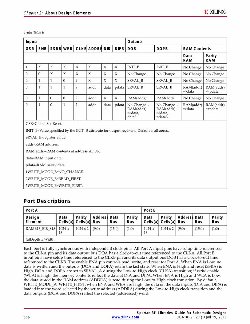
Chapter 2: About Design Elements
Truth Table B
Inputs Outputs
GSR ENB SSRB WEB CLKB ADDRB DIB DIPB DOB DOPB RAM ContentsDataRAM
ParityRAM
1 X X X X X X X INIT_B INIT_B No Change No Change
0 0 X X X X X X No Change No Change No Change No Change
0 1 1 0 ? X X X SRVAL_B SRVAL_B No Change No Change
0 1 1 1 ? addr data pdata SRVAL_B SRVAL_B RAM(addr)=>data
RAM(addr)=>pdata
0 1 0 0 ? addr X X RAM(addr) RAM(addr) No Change No Change
0 1 0 1 ? addr data pdata No Change1,RAM(addr)=>data,data3
No Change1,RAM(addr)=>data,pdata3
RAM(addr)=>data
RAM(addr)=>pdata
GSR=Global Set Reset.
INIT_B=Value specified by the INIT_B attribute for output registers. Default is all zeros.
SRVAL_B=register value.
addr=RAM address.
RAM(addr)=RAM contents at address ADDR.
data=RAM input data.
pdata=RAM parity data.
1WRITE_MODE_B=NO_CHANGE.
2WRITE_MODE_B=READ_FIRST.
3WRITE_MODE_B=WRITE_FIRST.
Port DescriptionsPort A Port BDesignElement
DataCells(a)
ParityCells(a)
AddressBus
DataBus
ParityBus
DataCells(a)
ParityCells(a)
AddressBus
DataBus
ParityBus
RAMB16_S18_S18 1024 x16
1024 x 2 (9:0) (15:0) (1:0) 1024 x16
1024 x 2 (9:0) (15:0) (1:0)
(a)Depth x Width
Each port is fully synchronous with independent clock pins. All Port A input pins have setup time referencedto the CLKA pin and its data output bus DOA has a clock-to-out time referenced to the CLKA. All Port Binput pins have setup time referenced to the CLKB pin and its data output bus DOB has a clock-to-out timereferenced to the CLKB. The enable ENA pin controls read, write, and reset for Port A. When ENA is Low, nodata is written and the outputs (DOA and DOPA) retain the last state. When ENA is High and reset (SSRA) isHigh, DOA and DOPA are set to SRVAL_A during the Low-to-High clock (CLKA) transition; if write enable(WEA) is High, the memory contents reflect the data at DIA and DIPA. When ENA is High and WEA is Low,the data stored in the RAM address (ADDRA) is read during the Low-to-High clock transition. By default,WRITE_MODE_A=WRITE_FIRST, when ENA and WEA are High, the data on the data inputs (DIA and DIPA) isloaded into the word selected by the write address (ADDRA) during the Low-to-High clock transition and thedata outputs (DOA and DOPA) reflect the selected (addressed) word.
Spartan-3E Libraries Guide for Schematic Designs556 www.xilinx.com UG618 (v 12.1) April 19, 2010
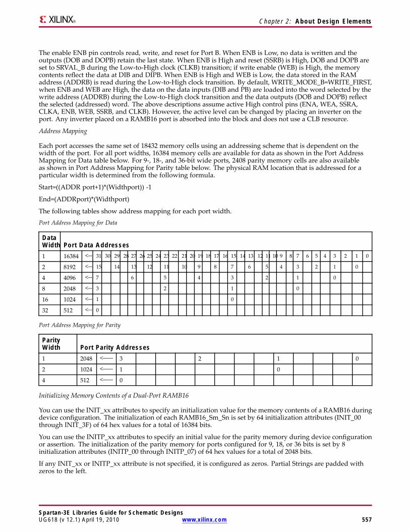
Chapter 2: About Design Elements
The enable ENB pin controls read, write, and reset for Port B. When ENB is Low, no data is written and theoutputs (DOB and DOPB) retain the last state. When ENB is High and reset (SSRB) is High, DOB and DOPB areset to SRVAL_B during the Low-to-High clock (CLKB) transition; if write enable (WEB) is High, the memorycontents reflect the data at DIB and DIPB. When ENB is High and WEB is Low, the data stored in the RAMaddress (ADDRB) is read during the Low-to-High clock transition. By default, WRITE_MODE_B=WRITE_FIRST,when ENB and WEB are High, the data on the data inputs (DIB and PB) are loaded into the word selected by thewrite address (ADDRB) during the Low-to-High clock transition and the data outputs (DOB and DOPB) reflectthe selected (addressed) word. The above descriptions assume active High control pins (ENA, WEA, SSRA,CLKA, ENB, WEB, SSRB, and CLKB). However, the active level can be changed by placing an inverter on theport. Any inverter placed on a RAMB16 port is absorbed into the block and does not use a CLB resource.
Address Mapping
Each port accesses the same set of 18432 memory cells using an addressing scheme that is dependent on thewidth of the port. For all port widths, 16384 memory cells are available for data as shown in the Port AddressMapping for Data table below. For 9-, 18-, and 36-bit wide ports, 2408 parity memory cells are also availableas shown in Port Address Mapping for Parity table below. The physical RAM location that is addressed for aparticular width is determined from the following formula.
Start=((ADDR port+1)*(Widthport)) -1
End=(ADDRport)*(Widthport)
The following tables show address mapping for each port width.
Port Address Mapping for Data
DataWidth Port Data Addresses1 16384 <-- 31 30 29 28 27 26 25 24 23 22 21 20 19 18 17 16 15 14 13 12 11 10 9 8 7 6 5 4 3 2 1 0
2 8192 <-- 15 14 13 12 11 10 9 8 7 6 5 4 3 2 1 0
4 4096 <-- 7 6 5 4 3 2 1 0
8 2048 <-- 3 2 1 0
16 1024 <-- 1 0
32 512 <-- 0
Port Address Mapping for Parity
ParityWidth Port Parity Addresses1 2048 <----- 3 2 1 0
2 1024 <----- 1 0
4 512 <----- 0
Initializing Memory Contents of a Dual-Port RAMB16
You can use the INIT_xx attributes to specify an initialization value for the memory contents of a RAMB16 duringdevice configuration. The initialization of each RAMB16_Sm_Sn is set by 64 initialization attributes (INIT_00through INIT_3F) of 64 hex values for a total of 16384 bits.
You can use the INITP_xx attributes to specify an initial value for the parity memory during device configurationor assertion. The initialization of the parity memory for ports configured for 9, 18, or 36 bits is set by 8initialization attributes (INITP_00 through INITP_07) of 64 hex values for a total of 2048 bits.
If any INIT_xx or INITP_xx attribute is not specified, it is configured as zeros. Partial Strings are padded withzeros to the left.
Spartan-3E Libraries Guide for Schematic DesignsUG618 (v 12.1) April 19, 2010 www.xilinx.com 557
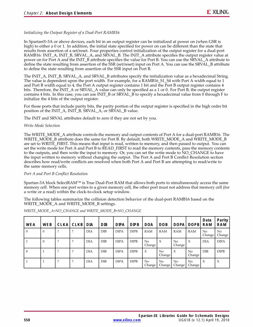
Chapter 2: About Design Elements
Initializing the Output Register of a Dual-Port RAMB16
In Spartan®-3A or above devices, each bit in an output register can be initialized at power on (when GSR ishigh) to either a 0 or 1. In addition, the initial state specified for power on can be different than the state thatresults from assertion of a set/reset. Four properties control initialization of the output register for a dual-portRAMB16: INIT_A, INIT_B, SRVAL_A, and SRVAL_B. The INIT_A attribute specifies the output register value atpower on for Port A and the INIT_B attribute specifies the value for Port B. You can use the SRVAL_A attribute todefine the state resulting from assertion of the SSR (set/reset) input on Port A. You can use the SRVAL_B attributeto define the state resulting from assertion of the SSR input on Port B.
The INIT_A, INIT_B, SRVAL_A, and SRVAL_B attributes specify the initialization value as a hexadecimal String.The value is dependent upon the port width. For example, for a RAMB16_S1_S4 with Port A width equal to 1and Port B width equal to 4, the Port A output register contains 1 bit and the Port B output register contains 4bits. Therefore, the INIT_A or SRVAL_A value can only be specified as a 1 or 0. For Port B, the output registercontains 4 bits. In this case, you can use INIT_B or SRVAL_B to specify a hexadecimal value from 0 through F toinitialize the 4 bits of the output register.
For those ports that include parity bits, the parity portion of the output register is specified in the high order bitposition of the INIT_A, INIT_B, SRVAL_A, or SRVAL_B value.
The INIT and SRVAL attributes default to zero if they are not set by you.
Write Mode Selection
TheWRITE_MODE_A attribute controls the memory and output contents of Port A for a dual-port RAMB16. TheWRITE_MODE_B attribute does the same for Port B. By default, both WRITE_MODE_A and WRITE_MODE_Bare set to WRITE_FIRST. This means that input is read, written to memory, and then passed to output. You canset the write mode for Port A and Port B to READ_FIRST to read the memory contents, pass the memory contentsto the outputs, and then write the input to memory. Or, you can set the write mode to NO_CHANGE to havethe input written to memory without changing the output. The Port A and Port B Conflict Resolution sectiondescribes how read/write conflicts are resolved when both Port A and Port B are attempting to read/write tothe same memory cells.
Port A and Port B Conflict Resolution
Spartan-3A block SelectRAM™ is True Dual-Port RAM that allows both ports to simultaneously access the samememory cell. When one port writes to a given memory cell, the other port must not address that memory cell (fora write or a read) within the clock-to-clock setup window.
The following tables summarize the collision detection behavior of the dual-port RAMB16 based on theWRITE_MODE_A and WRITE_MODE_B settings.
WRITE_MODE_A=NO_CHANGE and WRITE_MODE_B=NO_CHANGE
WEA WEB CLKA CLKB DIA DIB DIPA DIPB DOA DOB DOPA DOPBDataRAM
ParityRAM
0 0 ? ? DIA DIB DIPA DIPB RAM RAM RAM RAM NoChange
NoChange
1 0 ? ? DIA DIB DIPA DIPB NoChange
X NoChange
X DIA DIPA
0 1 ? ? DIA DIB DIPA DIPB X NoChange
X NoChange
DIB DIPB
1 1 ? ? DIA DIB DIPA DIPB NoChange
NoChange
NoChange
NoChange
X X
Spartan-3E Libraries Guide for Schematic Designs558 www.xilinx.com UG618 (v 12.1) April 19, 2010
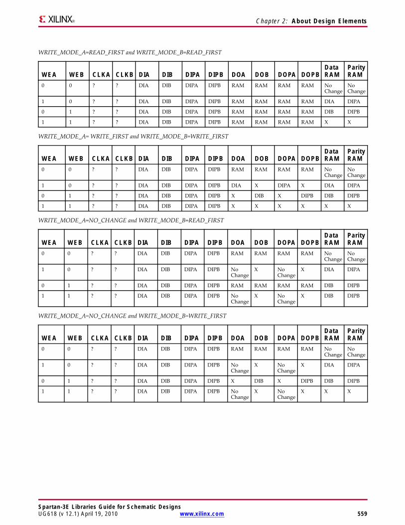
Chapter 2: About Design Elements
WRITE_MODE_A=READ_FIRST and WRITE_MODE_B=READ_FIRST
WEA WEB CLKA CLKB DIA DIB DIPA DIPB DOA DOB DOPA DOPBDataRAM
ParityRAM
0 0 ? ? DIA DIB DIPA DIPB RAM RAM RAM RAM NoChange
NoChange
1 0 ? ? DIA DIB DIPA DIPB RAM RAM RAM RAM DIA DIPA
0 1 ? ? DIA DIB DIPA DIPB RAM RAM RAM RAM DIB DIPB
1 1 ? ? DIA DIB DIPA DIPB RAM RAM RAM RAM X X
WRITE_MODE_A= WRITE_FIRST and WRITE_MODE_B=WRITE_FIRST
WEA WEB CLKA CLKB DIA DIB DIPA DIPB DOA DOB DOPA DOPBDataRAM
ParityRAM
0 0 ? ? DIA DIB DIPA DIPB RAM RAM RAM RAM NoChange
NoChange
1 0 ? ? DIA DIB DIPA DIPB DIA X DIPA X DIA DIPA
0 1 ? ? DIA DIB DIPA DIPB X DIB X DIPB DIB DIPB
1 1 ? ? DIA DIB DIPA DIPB X X X X X X
WRITE_MODE_A=NO_CHANGE and WRITE_MODE_B=READ_FIRST
WEA WEB CLKA CLKB DIA DIB DIPA DIPB DOA DOB DOPA DOPBDataRAM
ParityRAM
0 0 ? ? DIA DIB DIPA DIPB RAM RAM RAM RAM NoChange
NoChange
1 0 ? ? DIA DIB DIPA DIPB NoChange
X NoChange
X DIA DIPA
0 1 ? ? DIA DIB DIPA DIPB RAM RAM RAM RAM DIB DIPB
1 1 ? ? DIA DIB DIPA DIPB NoChange
X NoChange
X DIB DIPB
WRITE_MODE_A=NO_CHANGE and WRITE_MODE_B=WRITE_FIRST
WEA WEB CLKA CLKB DIA DIB DIPA DIPB DOA DOB DOPA DOPBDataRAM
ParityRAM
0 0 ? ? DIA DIB DIPA DIPB RAM RAM RAM RAM NoChange
NoChange
1 0 ? ? DIA DIB DIPA DIPB NoChange
X NoChange
X DIA DIPA
0 1 ? ? DIA DIB DIPA DIPB X DIB X DIPB DIB DIPB
1 1 ? ? DIA DIB DIPA DIPB NoChange
X NoChange
X X X
Spartan-3E Libraries Guide for Schematic DesignsUG618 (v 12.1) April 19, 2010 www.xilinx.com 559
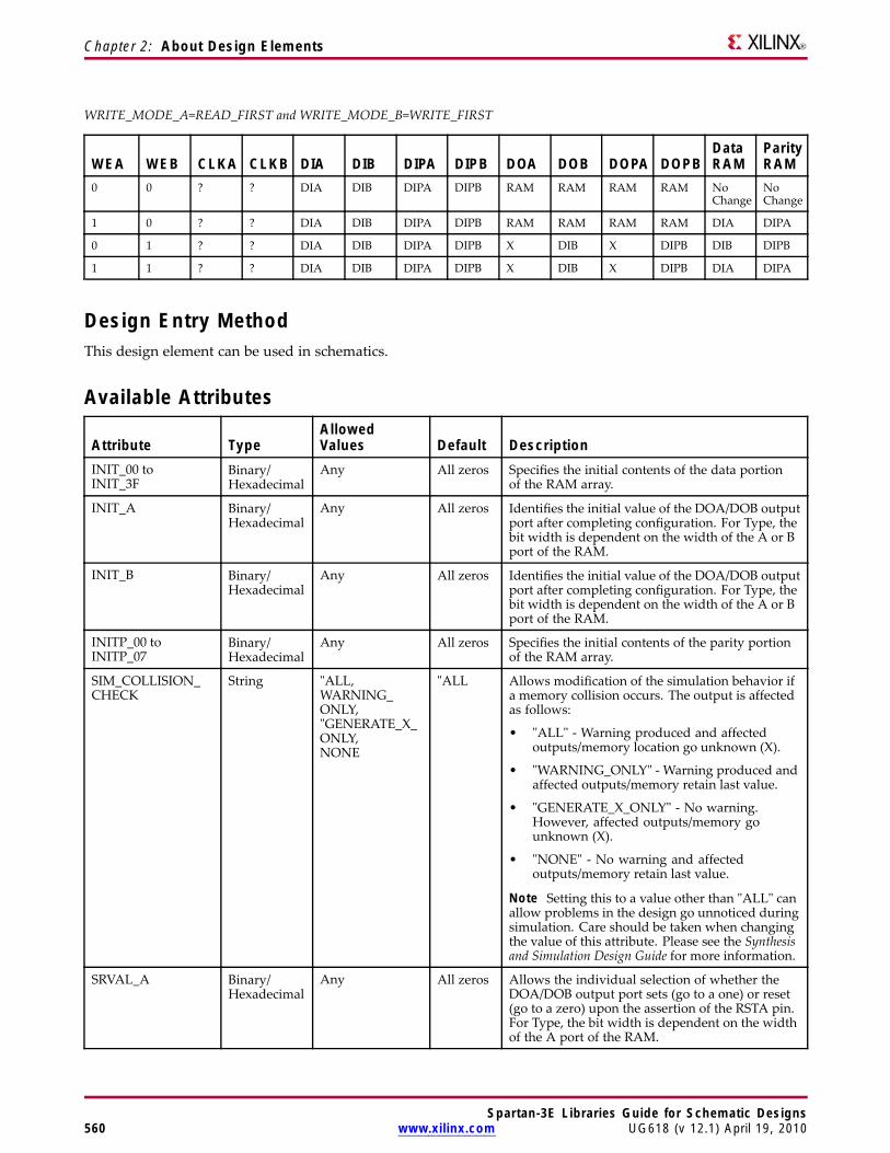
Chapter 2: About Design Elements
WRITE_MODE_A=READ_FIRST and WRITE_MODE_B=WRITE_FIRST
WEA WEB CLKA CLKB DIA DIB DIPA DIPB DOA DOB DOPA DOPBDataRAM
ParityRAM
0 0 ? ? DIA DIB DIPA DIPB RAM RAM RAM RAM NoChange
NoChange
1 0 ? ? DIA DIB DIPA DIPB RAM RAM RAM RAM DIA DIPA
0 1 ? ? DIA DIB DIPA DIPB X DIB X DIPB DIB DIPB
1 1 ? ? DIA DIB DIPA DIPB X DIB X DIPB DIA DIPA
Design Entry MethodThis design element can be used in schematics.
Available Attributes
Attribute TypeAllowedValues Default Description
INIT_00 toINIT_3F
Binary/Hexadecimal
Any All zeros Specifies the initial contents of the data portionof the RAM array.
INIT_A Binary/Hexadecimal
Any All zeros Identifies the initial value of the DOA/DOB outputport after completing configuration. For Type, thebit width is dependent on the width of the A or Bport of the RAM.
INIT_B Binary/Hexadecimal
Any All zeros Identifies the initial value of the DOA/DOB outputport after completing configuration. For Type, thebit width is dependent on the width of the A or Bport of the RAM.
INITP_00 toINITP_07
Binary/Hexadecimal
Any All zeros Specifies the initial contents of the parity portionof the RAM array.
SIM_COLLISION_CHECK
String "ALL,WARNING_ONLY,"GENERATE_X_ONLY,NONE
"ALL Allows modification of the simulation behavior ifa memory collision occurs. The output is affectedas follows:
• "ALL" - Warning produced and affectedoutputs/memory location go unknown (X).
• "WARNING_ONLY" - Warning produced andaffected outputs/memory retain last value.
• "GENERATE_X_ONLY" - No warning.However, affected outputs/memory gounknown (X).
• "NONE" - No warning and affectedoutputs/memory retain last value.
Note Setting this to a value other than "ALL" canallow problems in the design go unnoticed duringsimulation. Care should be taken when changingthe value of this attribute. Please see the Synthesisand Simulation Design Guide for more information.
SRVAL_A Binary/Hexadecimal
Any All zeros Allows the individual selection of whether theDOA/DOB output port sets (go to a one) or reset(go to a zero) upon the assertion of the RSTA pin.For Type, the bit width is dependent on the widthof the A port of the RAM.
Spartan-3E Libraries Guide for Schematic Designs560 www.xilinx.com UG618 (v 12.1) April 19, 2010

Chapter 2: About Design Elements
Attribute TypeAllowedValues Default Description
SRVAL_B Binary/Hexadecimal
Any All zeros Allows the individual selection of whether theDOA/DOB output port sets (go to a one) or reset(go to a zero) upon the assertion of the RSTB pin.For Type, the bit width is dependent on the widthof the B port of the RAM.
WRITE_MODE_A String "WRITE_FIRST","READ_FIRST","NO_CHANGE
"WRITE_FIRST
Specifies the behavior of the DOA/DOB port upona write command to the respected port. If set to"WRITE_FIRST", the same port that is writtento displays the contents of the written data tothe outputs upon completion of the operation."READ_FIRST" displays the prior contents of theRAM to the output port prior to writing the newdata. "NO_CHANGE" keeps the previous valueon the output port and wont update the outputport upon a write command. This is the suggestedmode if not using the read data from a particularport of the RAM.
WRITE_MODE_B String "WRITE_FIRST","READ_FIRST","NO_CHANGE
"WRITE_FIRST
Specifies the behavior of the DOA/DOB port upona write command to the respected port. If set to"WRITE_FIRST", the same port that is writtento displays the contents of the written data tothe outputs upon completion of the operation."READ_FIRST" displays the prior contents of theRAM to the output port prior to writing the newdata. "NO_CHANGE" keeps the previous valueon the output port and wont update the outputport upon a write command. This is the suggestedmode if not using the read data from a particularport of the RAM.
For More Information• See the Spartan-3 Generation FPGA User Guide.
• See the Spartan-3E FPGA Family Complete Data Sheet.
Spartan-3E Libraries Guide for Schematic DesignsUG618 (v 12.1) April 19, 2010 www.xilinx.com 561
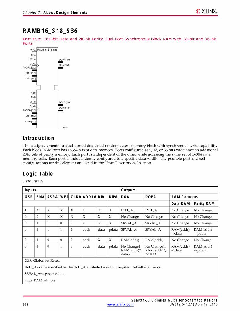
Chapter 2: About Design Elements
RAMB16_S18_S36Primitive: 16K-bit Data and 2K-bit Parity Dual-Port Synchronous Block RAM with 18-bit and 36-bitPorts
IntroductionThis design element is a dual-ported dedicated random access memory block with synchronous write capability.Each block RAM port has 16384 bits of data memory. Ports configured as 9, 18, or 36 bits wide have an additional2048 bits of parity memory. Each port is independent of the other while accessing the same set of 16384 datamemory cells. Each port is independently configured to a specific data width. The possible port and cellconfigurations for this element are listed in the "Port Descriptions" section.
Logic TableTruth Table A
Inputs Outputs
GSR ENA SSRA WEA CLKA ADDRA DIA DIPA DOA DOPA RAM ContentsData RAM Parity RAM
1 X X X X X X X INIT_A INIT_A No Change No Change
0 0 X X X X X X No Change No Change No Change No Change
0 1 1 0 ? X X X SRVAL_A SRVAL_A No Change No Change
0 1 1 1 ? addr data pdata SRVAL_A SRVAL_A RAM(addr)=>data
RAM(addr)=>pdata
0 1 0 0 ? addr X X RAM(addr) RAM(addr) No Change No Change
0 1 0 1 ? addr data pdata No Change1,RAM(addr)2,data3
No Change1,RAM(addr)2,pdata3
RAM(addr)=>data
RAM(addr)=>pdata
GSR=Global Set Reset.
INIT_A=Value specified by the INIT_A attribute for output register. Default is all zeros.
SRVAL_A=register value.
addr=RAM address.
Spartan-3E Libraries Guide for Schematic Designs562 www.xilinx.com UG618 (v 12.1) April 19, 2010
Chapter 2: About Design Elements
Inputs Outputs
GSR ENA SSRA WEA CLKA ADDRA DIA DIPA DOA DOPA RAM ContentsData RAM Parity RAM
RAM(addr)=RAM contents at address ADDR.
data=RAM input data.
pdata=RAM parity data.
1WRITE_MODE_A=NO_CHANGE.
2WRITE_MODE_A=READ_FIRST.
3WRITE_MODE_A=WRITE_FIRST.
Spartan-3E Libraries Guide for Schematic DesignsUG618 (v 12.1) April 19, 2010 www.xilinx.com 563

Chapter 2: About Design Elements
Truth Table B
Inputs Outputs
GSR ENB SSRB WEB CLKB ADDRB DIB DIPB DOB DOPB RAM ContentsDataRAM
ParityRAM
1 X X X X X X X INIT_B INIT_B No Change No Change
0 0 X X X X X X No Change No Change No Change No Change
0 1 1 0 ? X X X SRVAL_B SRVAL_B No Change No Change
0 1 1 1 ? addr data pdata SRVAL_B SRVAL_B RAM(addr)=>data
RAM(addr)=>pdata
0 1 0 0 ? addr X X RAM(addr) RAM(addr) No Change No Change
0 1 0 1 ? addr data pdata No Change1,RAM(addr)=>data,data3
No Change1,RAM(addr)=>data,pdata3
RAM(addr)=>data
RAM(addr)=>pdata
GSR=Global Set Reset.
INIT_B=Value specified by the INIT_B attribute for output registers. Default is all zeros.
SRVAL_B=register value.
addr=RAM address.
RAM(addr)=RAM contents at address ADDR.
data=RAM input data.
pdata=RAM parity data.
1WRITE_MODE_B=NO_CHANGE.
2WRITE_MODE_B=READ_FIRST.
3WRITE_MODE_B=WRITE_FIRST.
Port DescriptionsPort A Port BDesignElement
DataCells(a)
ParityCells(a)
AddressBus
DataBus
ParityBus
DataCells(a)
ParityCells(a)
AddressBus
DataBus
ParityBus
RAMB16_S18_S36 1024 x16
1024 x 2 (9:0) (15:0) (1:0) 512 x 32 512 x 4 (8:0) (31:0) (3:0)
(a)Depth x Width
Each port is fully synchronous with independent clock pins. All Port A input pins have setup time referencedto the CLKA pin and its data output bus DOA has a clock-to-out time referenced to the CLKA. All Port Binput pins have setup time referenced to the CLKB pin and its data output bus DOB has a clock-to-out timereferenced to the CLKB. The enable ENA pin controls read, write, and reset for Port A. When ENA is Low, nodata is written and the outputs (DOA and DOPA) retain the last state. When ENA is High and reset (SSRA) isHigh, DOA and DOPA are set to SRVAL_A during the Low-to-High clock (CLKA) transition; if write enable(WEA) is High, the memory contents reflect the data at DIA and DIPA. When ENA is High and WEA is Low,the data stored in the RAM address (ADDRA) is read during the Low-to-High clock transition. By default,WRITE_MODE_A=WRITE_FIRST, when ENA and WEA are High, the data on the data inputs (DIA and DIPA) isloaded into the word selected by the write address (ADDRA) during the Low-to-High clock transition and thedata outputs (DOA and DOPA) reflect the selected (addressed) word.
Spartan-3E Libraries Guide for Schematic Designs564 www.xilinx.com UG618 (v 12.1) April 19, 2010
Chapter 2: About Design Elements
The enable ENB pin controls read, write, and reset for Port B. When ENB is Low, no data is written and theoutputs (DOB and DOPB) retain the last state. When ENB is High and reset (SSRB) is High, DOB and DOPB areset to SRVAL_B during the Low-to-High clock (CLKB) transition; if write enable (WEB) is High, the memorycontents reflect the data at DIB and DIPB. When ENB is High and WEB is Low, the data stored in the RAMaddress (ADDRB) is read during the Low-to-High clock transition. By default, WRITE_MODE_B=WRITE_FIRST,when ENB and WEB are High, the data on the data inputs (DIB and PB) are loaded into the word selected by thewrite address (ADDRB) during the Low-to-High clock transition and the data outputs (DOB and DOPB) reflectthe selected (addressed) word. The above descriptions assume active High control pins (ENA, WEA, SSRA,CLKA, ENB, WEB, SSRB, and CLKB). However, the active level can be changed by placing an inverter on theport. Any inverter placed on a RAMB16 port is absorbed into the block and does not use a CLB resource.
Address Mapping
Each port accesses the same set of 18432 memory cells using an addressing scheme that is dependent on thewidth of the port. For all port widths, 16384 memory cells are available for data as shown in the Port AddressMapping for Data table below. For 9-, 18-, and 36-bit wide ports, 2408 parity memory cells are also availableas shown in Port Address Mapping for Parity table below. The physical RAM location that is addressed for aparticular width is determined from the following formula.
Start=((ADDR port+1)*(Widthport)) -1
End=(ADDRport)*(Widthport)
The following tables shows address mapping for each port width.
Port Address Mapping for Data
DataWidth Port Data Addresses1 16384 <-- 31 30 29 28 27 26 25 24 23 22 21 2019 18 17 161514 1312 11 10 9 8 7 6 5 4 3 2 1 0
2 8192 <-- 15 14 13 12 11 10 9 8 7 6 5 4 3 2 1 0
4 4096 <-- 7 6 5 4 3 2 1 0
8 2048 <-- 3 2 1 0
16 1024 <-- 1 0
32 512 <-- 0
Port Address Mapping for Parity
ParityWidth Port Parity Addresses1 2048 <-- 3 2 1 0
2 1024 <-- 1 0
4 512 <-- 0
Initializing Memory Contents of a Dual-Port RAMB16
You can use the INIT_xx attributes to specify an initialization value for the memory contents of a RAMB16 duringdevice configuration. The initialization of each RAMB16_Sm_Sn is set by 64 initialization attributes (INIT_00through INIT_3F) of 64 hex values for a total of 16384 bits.
You can use the INITP_xx attributes to specify an initial value for the parity memory during device configurationor assertion. The initialization of the parity memory for ports configured for 9, 18, or 36 bits is set by 8initialization attributes (INITP_00 through INITP_07) of 64 hex values for a total of 2048 bits.
If any INIT_xx or INITP_xx attribute is not specified, it is configured as zeros. Partial Strings are padded withzeros to the left.
Spartan-3E Libraries Guide for Schematic DesignsUG618 (v 12.1) April 19, 2010 www.xilinx.com 565
Chapter 2: About Design Elements
Initializing the Output Register of a Dual-Port RAMB16
In Spartan®-3A and above devices, each bit in an output register can be initialized at power on (when GSR ishigh) to either a 0 or 1. In addition, the initial state specified for power on can be different than the state thatresults from assertion of a set/reset. Four properties control initialization of the output register for a dual-portRAMB16: INIT_A, INIT_B, SRVAL_A, and SRVAL_B. The INIT_A attribute specifies the output register value atpower on for Port A and the INIT_B attribute specifies the value for Port B. You can use the SRVAL_A attribute todefine the state resulting from assertion of the SSR (set/reset) input on Port A. You can use the SRVAL_B attributeto define the state resulting from assertion of the SSR input on Port B.
The INIT_A, INIT_B, SRVAL_A, and SRVAL_B attributes specify the initialization value as a hexadecimal String.The value is dependent upon the port width. For example, for a RAMB16_S1_S4 with Port A width equal to 1and Port B width equal to 4, the Port A output register contains 1 bit and the Port B output register contains 4bits. Therefore, the INIT_A or SRVAL_A value can only be specified as a 1 or 0. For Port B, the output registercontains 4 bits. In this case, you can use INIT_B or SRVAL_B to specify a hexadecimal value from 0 through F toinitialize the 4 bits of the output register.
For those ports that include parity bits, the parity portion of the output register is specified in the high order bitposition of the INIT_A, INIT_B, SRVAL_A, or SRVAL_B value.
The INIT and SRVAL attributes default to zero if they are not set by you.
Write Mode Selection
TheWRITE_MODE_A attribute controls the memory and output contents of Port A for a dual-port RAMB16. TheWRITE_MODE_B attribute does the same for Port B. By default, both WRITE_MODE_A and WRITE_MODE_Bare set to WRITE_FIRST. This means that input is read, written to memory, and then passed to output. You canset the write mode for Port A and Port B to READ_FIRST to read the memory contents, pass the memory contentsto the outputs, and then write the input to memory. Or, you can set the write mode to NO_CHANGE to havethe input written to memory without changing the output. The Port A and Port B Conflict Resolution sectiondescribes how read/write conflicts are resolved when both Port A and Port B are attempting to read/write tothe same memory cells.
Port A and Port B Conflict Resolution
Spartan-3A block SelectRAM™ is True Dual-Port RAM that allows both ports to simultaneously access the samememory cell. When one port writes to a given memory cell, the other port must not address that memory cell (fora write or a read) within the clock-to-clock setup window.
The following tables summarize the collision detection behavior of the dual-port RAMB16 based on theWRITE_MODE_A and WRITE_MODE_B settings.
WRITE_MODE_A=NO_CHANGE and WRITE_MODE_B=NO_CHANGE
WEA WEB CLKA CLKB DIA DIB DIPA DIPB DOA DOB DOPA DOPBDataRAM
ParityRAM
0 0 ? ? DIA DIB DIPA DIPB RAM RAM RAM RAM NoChange
NoChange
1 0 ? ? DIA DIB DIPA DIPB NoChange
X NoChange
X DIA DIPA
0 1 ? ? DIA DIB DIPA DIPB X NoChange
X NoChange
DIB DIPB
1 1 ? ? DIA DIB DIPA DIPB NoChange
NoChange
NoChange
NoChange
X X
Spartan-3E Libraries Guide for Schematic Designs566 www.xilinx.com UG618 (v 12.1) April 19, 2010

Chapter 2: About Design Elements
WRITE_MODE_A=READ_FIRST and WRITE_MODE_B=READ_FIRST
WEA WEB CLKA CLKB DIA DIB DIPA DIPB DOA DOB DOPA DOPBDataRAM
ParityRAM
0 0 ? ? DIA DIB DIPA DIPB RAM RAM RAM RAM NoChange
NoChange
1 0 ? ? DIA DIB DIPA DIPB RAM RAM RAM RAM DIA DIPA
0 1 ? ? DIA DIB DIPA DIPB RAM RAM RAM RAM DIB DIPB
1 1 ? ? DIA DIB DIPA DIPB RAM RAM RAM RAM X X
WRITE_MODE_A= WRITE_FIRST and WRITE_MODE_B=WRITE_FIRST
WEA WEB CLKA CLKB DIA DIB DIPA DIPB DOA DOB DOPA DOPBDataRAM
ParityRAM
0 0 ? ? DIA DIB DIPA DIPB RAM RAM RAM RAM NoChange
NoChange
1 0 ? ? DIA DIB DIPA DIPB DIA X DIPA X DIA DIPA
0 1 ? ? DIA DIB DIPA DIPB X DIB X DIPB DIB DIPB
1 1 ? ? DIA DIB DIPA DIPB X X X X X X
WRITE_MODE_A=NO_CHANGE and WRITE_MODE_B=READ_FIRST
WEA WEB CLKA CLKB DIA DIB DIPA DIPB DOA DOB DOPA DOPBDataRAM
ParityRAM
0 0 ? ? DIA DIB DIPA DIPB RAM RAM RAM RAM NoChange
NoChange
1 0 ? ? DIA DIB DIPA DIPB NoChange
X NoChange
X DIA DIPA
0 1 ? ? DIA DIB DIPA DIPB RAM RAM RAM RAM DIB DIPB
1 1 ? ? DIA DIB DIPA DIPB NoChange
X NoChange
X DIB DIPB
WRITE_MODE_A=NO_CHANGE and WRITE_MODE_B=WRITE_FIRST
WEA WEB CLKA CLKB DIA DIB DIPA DIPB DOA DOB DOPA DOPBDataRAM
ParityRAM
0 0 ? ? DIA DIB DIPA DIPB RAM RAM RAM RAM NoChange
NoChange
1 0 ? ? DIA DIB DIPA DIPB NoChange
X NoChange
X DIA DIPA
0 1 ? ? DIA DIB DIPA DIPB X DIB X DIPB DIB DIPB
1 1 ? ? DIA DIB DIPA DIPB NoChange
X NoChange
X X X
Spartan-3E Libraries Guide for Schematic DesignsUG618 (v 12.1) April 19, 2010 www.xilinx.com 567
Chapter 2: About Design Elements
WRITE_MODE_A=READ_FIRST and WRITE_MODE_B=WRITE_FIRST
WEA WEB CLKA CLKB DIA DIB DIPA DIPB DOA DOB DOPA DOPBDataRAM
ParityRAM
0 0 ? ? DIA DIB DIPA DIPB RAM RAM RAM RAM NoChange
NoChange
1 0 ? ? DIA DIB DIPA DIPB RAM RAM RAM RAM DIA DIPA
0 1 ? ? DIA DIB DIPA DIPB X DIB X DIPB DIB DIPB
1 1 ? ? DIA DIB DIPA DIPB X DIB X DIPB DIA DIPA
Design Entry MethodThis design element can be used in schematics.
Available Attributes
Attribute TypeAllowedValues Default Description
INIT_00 toINIT_3F
Binary/Hexadecimal
Any All zeros Specifies the initial contents of the data portionof the RAM array.
INIT_A Binary/Hexadecimal
Any All zeros Identifies the initial value of the DOA/DOB outputport after completing configuration. For Type, thebit width is dependent on the width of the A or Bport of the RAM.
INIT_B Binary/Hexadecimal
Any All zeros Identifies the initial value of the DOA/DOB outputport after completing configuration. For Type, thebit width is dependent on the width of the A or Bport of the RAM.
INITP_00 toINITP_07
Binary/Hexadecimal
Any All zeros Specifies the initial contents of the parity portionof the RAM array.
SIM_COLLISION_CHECK
String "ALL,WARNING_ONLY,"GENERATE_X_ONLY,NONE
"ALL Allows modification of the simulation behavior ifa memory collision occurs. The output is affectedas follows:
• "ALL" - Warning produced and affectedoutputs/memory location go unknown (X).
• "WARNING_ONLY" - Warning produced andaffected outputs/memory retain last value.
• "GENERATE_X_ONLY" - No warning.However, affected outputs/memory gounknown (X).
• "NONE" - No warning and affectedoutputs/memory retain last value.
Note Setting this to a value other than "ALL" canallow problems in the design go unnoticed duringsimulation. Care should be taken when changingthe value of this attribute. Please see the Synthesisand Simulation Design Guide for more information.
SRVAL_A Binary/Hexadecimal
Any All zeros Allows the individual selection of whether theDOA/DOB output port sets (go to a one) or reset(go to a zero) upon the assertion of the RSTA pin.For Type, the bit width is dependent on the widthof the A port of the RAM.
Spartan-3E Libraries Guide for Schematic Designs568 www.xilinx.com UG618 (v 12.1) April 19, 2010
Chapter 2: About Design Elements
Attribute TypeAllowedValues Default Description
SRVAL_B Binary/Hexadecimal
Any All zeros Allows the individual selection of whether theDOA/DOB output port sets (go to a one) or reset(go to a zero) upon the assertion of the RSTB pin.For Type, the bit width is dependent on the widthof the B port of the RAM.
WRITE_MODE_A String "WRITE_FIRST","READ_FIRST","NO_CHANGE
"WRITE_FIRST
Specifies the behavior of the DOA/DOB port upona write command to the respected port. If set to"WRITE_FIRST", the same port that is writtento displays the contents of the written data tothe outputs upon completion of the operation."READ_FIRST" displays the prior contents of theRAM to the output port prior to writing the newdata. "NO_CHANGE" keeps the previous valueon the output port and wont update the outputport upon a write command. This is the suggestedmode if not using the read data from a particularport of the RAM.
WRITE_MODE_B String "WRITE_FIRST","READ_FIRST","NO_CHANGE
"WRITE_FIRST
Specifies the behavior of the DOA/DOB port upona write command to the respected port. If set to"WRITE_FIRST", the same port that is writtento displays the contents of the written data tothe outputs upon completion of the operation."READ_FIRST" displays the prior contents of theRAM to the output port prior to writing the newdata. "NO_CHANGE" keeps the previous valueon the output port and wont update the outputport upon a write command. This is the suggestedmode if not using the read data from a particularport of the RAM.
For More Information• See the Spartan-3 Generation FPGA User Guide.
• See the Spartan-3E FPGA Family Complete Data Sheet.
Spartan-3E Libraries Guide for Schematic DesignsUG618 (v 12.1) April 19, 2010 www.xilinx.com 569
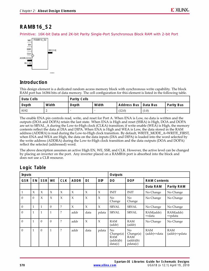
Chapter 2: About Design Elements
RAMB16_S2Primitive: 16K-bit Data and 2K-bit Parity Single-Port Synchronous Block RAM with 2-bit Port
IntroductionThis design element is a dedicated random access memory block with synchronous write capability. The blockRAM port has 16384 bits of data memory. The cell configuration for this element is listed in the following table.
Data Cells Parity CellsDepth Width Depth Width Address Bus Data Bus Parity Bus8192 2 - - (12:0) (1:0) -
The enable ENA pin controls read, write, and reset for Port A. When ENA is Low, no data is written and theoutputs (DOA and DOPA) retain the last state. When ENA is High and reset (SSRA) is High, DOA and DOPAare set to SRVAL_A during the Low-to-High clock (CLKA) transition; if write enable (WEA) is High, the memorycontents reflect the data at DIA and DIPA. When ENA is High and WEA is Low, the data stored in the RAMaddress (ADDRA) is read during the Low-to-High clock transition. By default, WRITE_MODE_A=WRITE_FIRST,when ENA and WEA are High, the data on the data inputs (DIA and DIPA) is loaded into the word selected bythe write address (ADDRA) during the Low-to-High clock transition and the data outputs (DOA and DOPA)reflect the selected (addressed) word.
The above description assumes an active High EN, WE, SSR, and CLK. However, the active level can be changedby placing an inverter on the port. Any inverter placed on a RAMB16 port is absorbed into the block anddoes not use a CLB resource.
Logic TableInputs Outputs
GSR EN SSR WE CLK ADDR DI DIP DO DOP RAM ContentsData RAM Parity RAM
1 X X X X X X X INIT INIT No Change No Change
0 0 X X X X X X NoChange
NoChange
No Change No Change
0 1 1 0 ? X X X SRVAL SRVAL No Change No Change
0 1 1 1 ? addr data pdata SRVAL SRVAL RAM(addr)=>data
RAM(addr)=>pdata
0 1 0 0 ? addr X X RAM(addr)
RAM(addr)
No Change No Change
0 1 0 1 ? addr data pdata NoChange(a)RAM(addr)(b)data(c)
NoChange(a)RAM(addr)(b)pdata(c)
RAM(addr)=>data
RAM(addr)=>pdata
Spartan-3E Libraries Guide for Schematic Designs570 www.xilinx.com UG618 (v 12.1) April 19, 2010
Chapter 2: About Design Elements
Inputs Outputs
GSR EN SSR WE CLK ADDR DI DIP DO DOP RAM ContentsData RAM Parity RAM
GSR=Global Set Reset signal
INIT=Value specified by the INIT attribute for data memory. Default is all zeros.
SRVAL=Value after assertion of SSR as specified by the SRVAL attribute.
addr=RAM address.
RAM(addr)=RAM contents at address ADDR.
data=RAM input data.
pdata=RAM parity data.
(a) WRITE_MODE=NO_CHANGE
(b) WRITE_MODE=READ_FIRST
(c) WRITE_MODE=WRITE_FIRST
InitializationInitializing Memory Contents
You can use the INIT_xx attributes to specify an initialization value for the memory contents of a RAMB16 duringdevice configuration. The initialization of each RAMB16 is set by 64 initialization attributes (INIT_00 throughINIT_3F) of 64 hex values for a total of 16384 bits.
You can use the INITP_xx attributes to specify an initial value for the parity memory during device configurationor assertion. The initialization of the parity memory for ports configured for 9, 18, or 36 bits is set by 8initialization attributes (INITP_00 through INITP_07) of 64 hex values for a total of 2048 bits.
Any INIT_xx or INITP_xx attribute that is not specified is configured as zeros. Partial Strings are paddedwith zeros to the left.
Initializing the Output Register
In Spartan®-3A and above devices, each bit in the output register can be initialized at power on to either a 0 or 1.In addition, the initial state specified for power on can be different than the state that results from assertion of aset/reset. Two types of properties control initialization of the output register for a single-port RAMB16: INIT andSRVAL. The INIT attribute specifies the output register value at power on. You can use the SRVAL attributeto define the state resulting from assertion of the SSR (set/reset) input.
The INIT and SRVAL attributes specify the initialization value as a hexadecimal String containing one bit foreach bit in the output port. For example, for a RAMB16_S1 with port width equal to 1, the output registercontains 1 bit. Therefore, the INIT or SRVAL value can only be specified as a 1 or 0. For RAMB16_S4 with portwidth equal to 4, the output register contains 4 bits. In this case, you can specify a hexadecimal value from 0through F to initialize the 4 bits of the output register.
For those ports that include parity bits, the parity portion of the output register is specified in the high orderbit position of the INIT or SRVAL value.
Selecting Write Mode
The WRITE_MODE attribute controls RAMB16 memory and output contents. By default, the WRITE_MODE isset to WRITE_FIRST. This means that input is read, written to memory, and then passed to output. You can setthe WRITE_MODE to READ_FIRST to read the memory contents, pass the memory contents to the outputs, andthen write the input to memory. Or, you can set the WRITE_MODE to NO_CHANGE to have the input writtento memory without changing the output.
Spartan-3E Libraries Guide for Schematic DesignsUG618 (v 12.1) April 19, 2010 www.xilinx.com 571
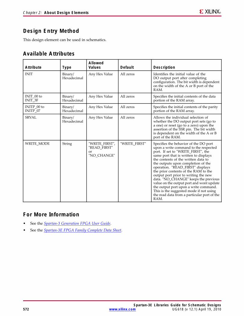
Chapter 2: About Design Elements
Design Entry MethodThis design element can be used in schematics.
Available Attributes
Attribute TypeAllowedValues Default Description
INIT Binary/Hexadecimal
Any Hex Value All zeros Identifies the initial value of theDO output port after completingconfiguration. The bit width is dependenton the width of the A or B port of theRAM.
INIT_00 toINIT_3F
Binary/Hexadecimal
Any Hex Value All zeros Specifies the initial contents of the dataportion of the RAM array.
INITP_00 toINITP_07
Binary/Hexadecimal
Any Hex Value All zeros Specifies the initial contents of the parityportion of the RAM array.
SRVAL Binary/Hexadecimal
Any Hex Value All zeros Allows the individual selection ofwhether the DO output port sets (go toa one) or reset (go to a zero) upon theassertion of the SSR pin. The bit widthis dependent on the width of the A or Bport of the RAM.
WRITE_MODE String "WRITE_FIRST","READ_FIRST"or"NO_CHANGE"
"WRITE_FIRST" Specifies the behavior of the DO portupon a write command to the respectedport. If set to "WRITE_FIRST", thesame port that is written to displaysthe contents of the written data tothe outputs upon completion of theoperation. "READ_FIRST" displaysthe prior contents of the RAM to theoutput port prior to writing the newdata. "NO_CHANGE" keeps the previousvalue on the output port and wont updatethe output port upon a write command.This is the suggested mode if not usingthe read data from a particular port of theRAM.
For More Information• See the Spartan-3 Generation FPGA User Guide.
• See the Spartan-3E FPGA Family Complete Data Sheet.
Spartan-3E Libraries Guide for Schematic Designs572 www.xilinx.com UG618 (v 12.1) April 19, 2010

Spartan-3E Libraries Guide for Schematic Designs573 www.xilinx.com UG618 (v 12.1) April 19, 2010

Chapter 2: About Design Elements
RAMB16_S2_S18Primitive: 16K-bit Data and 2K-bit Parity Dual-Port Synchronous Block RAM with 2-bit and 18-bitPorts
IntroductionThis design element is a dual-ported dedicated random access memory block with synchronous write capability.Each block RAM port has 16384 bits of data memory. Ports configured as 9, 18, or 36 bits wide have an additional2048 bits of parity memory. Each port is independent of the other while accessing the same set of 16384 datamemory cells. Each port is independently configured to a specific data width. The possible port and cellconfigurations for this element are listed in the "Port Descriptions" section.
Logic TableTruth Table A
Inputs Outputs
GSR ENA SSRA WEA CLKA ADDRA DIA DIPA DOA DOPA RAM ContentsData RAM Parity RAM
1 X X X X X X X INIT_A INIT_A No Change No Change
0 0 X X X X X X No Change No Change No Change No Change
0 1 1 0 ? X X X SRVAL_A SRVAL_A No Change No Change
0 1 1 1 ? addr data pdata SRVAL_A SRVAL_A RAM(addr)=>data
RAM(addr)=>pdata
0 1 0 0 ? addr X X RAM(addr) RAM(addr) No Change No Change
0 1 0 1 ? addr data pdata No Change1,RAM(addr)2,data3
No Change1,RAM(addr)2,pdata3
RAM(addr)=>data
RAM(addr)=>pdata
GSR=Global Set Reset.
INIT_A=Value specified by the INIT_A attribute for output register. Default is all zeros.
SRVAL_A=register value.
addr=RAM address.
RAM(addr)=RAM contents at address ADDR.
data=RAM input data.
Spartan-3E Libraries Guide for Schematic Designs574 www.xilinx.com UG618 (v 12.1) April 19, 2010

Chapter 2: About Design Elements
Inputs Outputs
GSR ENA SSRA WEA CLKA ADDRA DIA DIPA DOA DOPA RAM ContentsData RAM Parity RAM
pdata=RAM parity data.
1WRITE_MODE_A=NO_CHANGE.
2WRITE_MODE_A=READ_FIRST.
3WRITE_MODE_A=WRITE_FIRST.
Spartan-3E Libraries Guide for Schematic DesignsUG618 (v 12.1) April 19, 2010 www.xilinx.com 575

Chapter 2: About Design Elements
Truth Table B
Inputs Outputs
GSR ENB SSRB WEB CLKB ADDRB DIB DIPB DOB DOPB RAM ContentsDataRAM
ParityRAM
1 X X X X X X X INIT_B INIT_B No Change No Change
0 0 X X X X X X No Change No Change No Change No Change
0 1 1 0 ? X X X SRVAL_B SRVAL_B No Change No Change
0 1 1 1 ? addr data pdata SRVAL_B SRVAL_B RAM(addr)=>data
RAM(addr)=>pdata
0 1 0 0 ? addr X X RAM(addr) RAM(addr) No Change No Change
0 1 0 1 ? addr data pdata No Change1,RAM(addr)=>data,data3
No Change1,RAM(addr)=>data,pdata3
RAM(addr)=>data
RAM(addr)=>pdata
GSR=Global Set Reset.
INIT_B=Value specified by the INIT_B attribute for output registers. Default is all zeros.
SRVAL_B=register value.
addr=RAM address.
RAM(addr)=RAM contents at address ADDR.
data=RAM input data.
pdata=RAM parity data.
1WRITE_MODE_B=NO_CHANGE.
2WRITE_MODE_B=READ_FIRST.
3WRITE_MODE_B=WRITE_FIRST.
Port DescriptionsPort A Port BDesignElement
DataCells(a)
ParityCells(a)
AddressBus
DataBus
ParityBus
DataCells(a)
ParityCells(a)
AddressBus
DataBus
ParityBus
RAMB16_S2_S18 8192 x 2 - (12:0) (1:0) - 1024 x16
1024 x 2 (9:0) (15:0) (1:0)
(a)Depth x Width
Each port is fully synchronous with independent clock pins. All Port A input pins have setup time referencedto the CLKA pin and its data output bus DOA has a clock-to-out time referenced to the CLKA. All Port Binput pins have setup time referenced to the CLKB pin and its data output bus DOB has a clock-to-out timereferenced to the CLKB. The enable ENA pin controls read, write, and reset for Port A. When ENA is Low, nodata is written and the outputs (DOA and DOPA) retain the last state. When ENA is High and reset (SSRA) isHigh, DOA and DOPA are set to SRVAL_A during the Low-to-High clock (CLKA) transition; if write enable(WEA) is High, the memory contents reflect the data at DIA and DIPA. When ENA is High and WEA is Low,the data stored in the RAM address (ADDRA) is read during the Low-to-High clock transition. By default,WRITE_MODE_A=WRITE_FIRST, when ENA and WEA are High, the data on the data inputs (DIA and DIPA) isloaded into the word selected by the write address (ADDRA) during the Low-to-High clock transition and thedata outputs (DOA and DOPA) reflect the selected (addressed) word.
Spartan-3E Libraries Guide for Schematic Designs576 www.xilinx.com UG618 (v 12.1) April 19, 2010
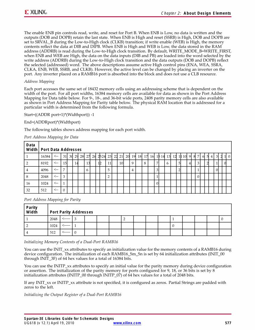
Chapter 2: About Design Elements
The enable ENB pin controls read, write, and reset for Port B. When ENB is Low, no data is written and theoutputs (DOB and DOPB) retain the last state. When ENB is High and reset (SSRB) is High, DOB and DOPB areset to SRVAL_B during the Low-to-High clock (CLKB) transition; if write enable (WEB) is High, the memorycontents reflect the data at DIB and DIPB. When ENB is High and WEB is Low, the data stored in the RAMaddress (ADDRB) is read during the Low-to-High clock transition. By default, WRITE_MODE_B=WRITE_FIRST,when ENB and WEB are High, the data on the data inputs (DIB and PB) are loaded into the word selected by thewrite address (ADDRB) during the Low-to-High clock transition and the data outputs (DOB and DOPB) reflectthe selected (addressed) word. The above descriptions assume active High control pins (ENA, WEA, SSRA,CLKA, ENB, WEB, SSRB, and CLKB). However, the active level can be changed by placing an inverter on theport. Any inverter placed on a RAMB16 port is absorbed into the block and does not use a CLB resource.
Address Mapping
Each port accesses the same set of 18432 memory cells using an addressing scheme that is dependent on thewidth of the port. For all port widths, 16384 memory cells are available for data as shown in the Port AddressMapping for Data table below. For 9-, 18-, and 36-bit wide ports, 2408 parity memory cells are also availableas shown in Port Address Mapping for Parity table below. The physical RAM location that is addressed for aparticular width is determined from the following formula.
Start=((ADDR port+1)*(Widthport)) -1
End=(ADDRport)*(Widthport)
The following tables shows address mapping for each port width.
Port Address Mapping for Data
DataWidth Port Data Addresses1 16384 <-- 31 30 29 28 27 26 2524 23 22 21 20 19 18 17 16 15 14 13 12 11 10 9 8 7 6 5 4 3 2 1 0
2 8192 <-- 15 14 13 12 11 10 9 8 7 6 5 4 3 2 1 0
4 4096 <-- 7 6 5 4 3 2 1 0
8 2048 <-- 3 2 1 0
16 1024 <-- 1 0
32 512 <-- 0
Port Address Mapping for Parity
ParityWidth Port Parity Addresses1 2048 <----- 3 2 1 0
2 1024 <----- 1 0
4 512 <----- 0
Initializing Memory Contents of a Dual-Port RAMB16
You can use the INIT_xx attributes to specify an initialization value for the memory contents of a RAMB16 duringdevice configuration. The initialization of each RAMB16_Sm_Sn is set by 64 initialization attributes (INIT_00through INIT_3F) of 64 hex values for a total of 16384 bits.
You can use the INITP_xx attributes to specify an initial value for the parity memory during device configurationor assertion. The initialization of the parity memory for ports configured for 9, 18, or 36 bits is set by 8initialization attributes (INITP_00 through INITP_07) of 64 hex values for a total of 2048 bits.
If any INIT_xx or INITP_xx attribute is not specified, it is configured as zeros. Partial Strings are padded withzeros to the left.
Initializing the Output Register of a Dual-Port RAMB16
Spartan-3E Libraries Guide for Schematic DesignsUG618 (v 12.1) April 19, 2010 www.xilinx.com 577

Chapter 2: About Design Elements
In Spartan®-3A and above devices, each bit in an output register can be initialized at power on (when GSR ishigh) to either a 0 or 1. In addition, the initial state specified for power on can be different than the state thatresults from assertion of a set/reset. Four properties control initialization of the output register for a dual-portRAMB16: INIT_A, INIT_B, SRVAL_A, and SRVAL_B. The INIT_A attribute specifies the output register value atpower on for Port A and the INIT_B attribute specifies the value for Port B. You can use the SRVAL_A attribute todefine the state resulting from assertion of the SSR (set/reset) input on Port A. You can use the SRVAL_B attributeto define the state resulting from assertion of the SSR input on Port B.
The INIT_A, INIT_B, SRVAL_A, and SRVAL_B attributes specify the initialization value as a hexadecimal String.The value is dependent upon the port width. For example, for a RAMB16_S1_S4 with Port A width equal to 1and Port B width equal to 4, the Port A output register contains 1 bit and the Port B output register contains 4bits. Therefore, the INIT_A or SRVAL_A value can only be specified as a 1 or 0. For Port B, the output registercontains 4 bits. In this case, you can use INIT_B or SRVAL_B to specify a hexadecimal value from 0 through F toinitialize the 4 bits of the output register.
For those ports that include parity bits, the parity portion of the output register is specified in the high order bitposition of the INIT_A, INIT_B, SRVAL_A, or SRVAL_B value.
The INIT and SRVAL attributes default to zero if they are not set by you.
Write Mode Selection
TheWRITE_MODE_A attribute controls the memory and output contents of Port A for a dual-port RAMB16. TheWRITE_MODE_B attribute does the same for Port B. By default, both WRITE_MODE_A and WRITE_MODE_Bare set to WRITE_FIRST. This means that input is read, written to memory, and then passed to output. You canset the write mode for Port A and Port B to READ_FIRST to read the memory contents, pass the memory contentsto the outputs, and then write the input to memory. Or, you can set the write mode to NO_CHANGE to havethe input written to memory without changing the output. The Port A and Port B Conflict Resolution sectiondescribes how read/write conflicts are resolved when both Port A and Port B are attempting to read/write tothe same memory cells.
Port A and Port B Conflict Resolution
Spartan-3A block SelectIO™ is True Dual-Port RAM that allows both ports to simultaneously access the samememory cell. When one port writes to a given memory cell, the other port must not address that memory cell (fora write or a read) within the clock-to-clock setup window.
The following tables summarize the collision detection behavior of the dual-port RAMB16 based on theWRITE_MODE_A and WRITE_MODE_B settings.
WRITE_MODE_A=NO_CHANGE and WRITE_MODE_B=NO_CHANGE
WEA WEB CLKA CLKB DIA DIB DIPA DIPB DOA DOB DOPA DOPBDataRAM
ParityRAM
0 0 ? ? DIA DIB DIPA DIPB RAM RAM RAM RAM NoChange
NoChange
1 0 ? ? DIA DIB DIPA DIPB NoChange
X NoChange
X DIA DIPA
0 1 ? ? DIA DIB DIPA DIPB X NoChange
X NoChange
DIB DIPB
1 1 ? ? DIA DIB DIPA DIPB NoChange
NoChange
NoChange
NoChange
X X
WRITE_MODE_A=READ_FIRST and WRITE_MODE_B=READ_FIRST
Spartan-3E Libraries Guide for Schematic Designs578 www.xilinx.com UG618 (v 12.1) April 19, 2010
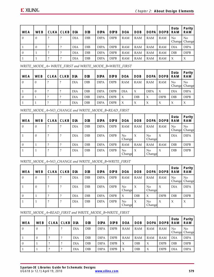
Chapter 2: About Design Elements
WEA WEB CLKA CLKB DIA DIB DIPA DIPB DOA DOB DOPA DOPBDataRAM
ParityRAM
0 0 ? ? DIA DIB DIPA DIPB RAM RAM RAM RAM NoChange
NoChange
1 0 ? ? DIA DIB DIPA DIPB RAM RAM RAM RAM DIA DIPA
0 1 ? ? DIA DIB DIPA DIPB RAM RAM RAM RAM DIB DIPB
1 1 ? ? DIA DIB DIPA DIPB RAM RAM RAM RAM X X
WRITE_MODE_A= WRITE_FIRST and WRITE_MODE_B=WRITE_FIRST
WEA WEB CLKA CLKB DIA DIB DIPA DIPB DOA DOB DOPA DOPBDataRAM
ParityRAM
0 0 ? ? DIA DIB DIPA DIPB RAM RAM RAM RAM NoChange
NoChange
1 0 ? ? DIA DIB DIPA DIPB DIA X DIPA X DIA DIPA
0 1 ? ? DIA DIB DIPA DIPB X DIB X DIPB DIB DIPB
1 1 ? ? DIA DIB DIPA DIPB X X X X X X
WRITE_MODE_A=NO_CHANGE and WRITE_MODE_B=READ_FIRST
WEA WEB CLKA CLKB DIA DIB DIPA DIPB DOA DOB DOPA DOPBDataRAM
ParityRAM
0 0 ? ? DIA DIB DIPA DIPB RAM RAM RAM RAM NoChange
NoChange
1 0 ? ? DIA DIB DIPA DIPB NoChange
X NoChange
X DIA DIPA
0 1 ? ? DIA DIB DIPA DIPB RAM RAM RAM RAM DIB DIPB
1 1 ? ? DIA DIB DIPA DIPB NoChange
X NoChange
X DIB DIPB
WRITE_MODE_A=NO_CHANGE and WRITE_MODE_B=WRITE_FIRST
WEA WEB CLKA CLKB DIA DIB DIPA DIPB DOA DOB DOPA DOPBDataRAM
ParityRAM
0 0 ? ? DIA DIB DIPA DIPB RAM RAM RAM RAM NoChange
NoChange
1 0 ? ? DIA DIB DIPA DIPB NoChange
X NoChange
X DIA DIPA
0 1 ? ? DIA DIB DIPA DIPB X DIB X DIPB DIB DIPB
1 1 ? ? DIA DIB DIPA DIPB NoChange
X NoChange
X X X
WRITE_MODE_A=READ_FIRST and WRITE_MODE_B=WRITE_FIRST
WEA WEB CLKA CLKB DIA DIB DIPA DIPB DOA DOB DOPA DOPBDataRAM
ParityRAM
0 0 ? ? DIA DIB DIPA DIPB RAM RAM RAM RAM NoChange
NoChange
1 0 ? ? DIA DIB DIPA DIPB RAM RAM RAM RAM DIA DIPA
0 1 ? ? DIA DIB DIPA DIPB X DIB X DIPB DIB DIPB
1 1 ? ? DIA DIB DIPA DIPB X DIB X DIPB DIA DIPA
Spartan-3E Libraries Guide for Schematic DesignsUG618 (v 12.1) April 19, 2010 www.xilinx.com 579

Chapter 2: About Design Elements
Design Entry MethodThis design element can be used in schematics.
Available Attributes
Attribute TypeAllowedValues Default Description
INIT_00 toINIT_3F
Binary/Hexadecimal
Any All zeros Specifies the initial contents of the data portionof the RAM array.
INIT_A Binary/Hexadecimal
Any All zeros Identifies the initial value of the DOA/DOB outputport after completing configuration. For Type, thebit width is dependent on the width of the A or Bport of the RAM.
INIT_B Binary/Hexadecimal
Any All zeros Identifies the initial value of the DOA/DOB outputport after completing configuration. For Type, thebit width is dependent on the width of the A or Bport of the RAM.
INITP_00 toINITP_07
Binary/Hexadecimal
Any All zeros Specifies the initial contents of the parity portionof the RAM array.
SIM_COLLISION_CHECK
String "ALL,WARNING_ONLY,"GENERATE_X_ONLY,NONE
"ALL Allows modification of the simulation behavior ifa memory collision occurs. The output is affectedas follows:
• "ALL" - Warning produced and affectedoutputs/memory location go unknown (X).
• "WARNING_ONLY" - Warning produced andaffected outputs/memory retain last value.
• "GENERATE_X_ONLY" - No warning.However, affected outputs/memory gounknown (X).
• "NONE" - No warning and affectedoutputs/memory retain last value.
Note Setting this to a value other than "ALL" canallow problems in the design go unnoticed duringsimulation. Care should be taken when changingthe value of this attribute. Please see the Synthesisand Simulation Design Guide for more information.
SRVAL_A Binary/Hexadecimal
Any All zeros Allows the individual selection of whether theDOA/DOB output port sets (go to a one) or reset(go to a zero) upon the assertion of the RSTA pin.For Type, the bit width is dependent on the widthof the A port of the RAM.
SRVAL_B Binary/Hexadecimal
Any All zeros Allows the individual selection of whether theDOA/DOB output port sets (go to a one) or reset(go to a zero) upon the assertion of the RSTB pin.For Type, the bit width is dependent on the widthof the B port of the RAM.
Spartan-3E Libraries Guide for Schematic Designs580 www.xilinx.com UG618 (v 12.1) April 19, 2010
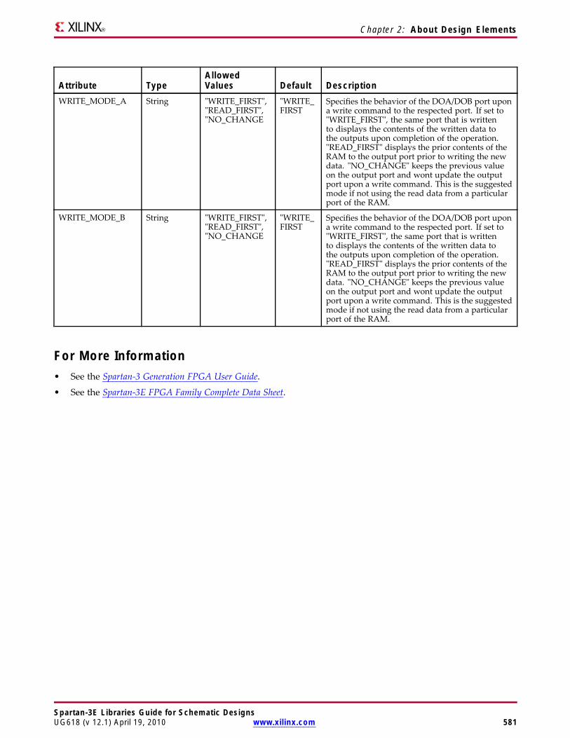
Chapter 2: About Design Elements
Attribute TypeAllowedValues Default Description
WRITE_MODE_A String "WRITE_FIRST","READ_FIRST","NO_CHANGE
"WRITE_FIRST
Specifies the behavior of the DOA/DOB port upona write command to the respected port. If set to"WRITE_FIRST", the same port that is writtento displays the contents of the written data tothe outputs upon completion of the operation."READ_FIRST" displays the prior contents of theRAM to the output port prior to writing the newdata. "NO_CHANGE" keeps the previous valueon the output port and wont update the outputport upon a write command. This is the suggestedmode if not using the read data from a particularport of the RAM.
WRITE_MODE_B String "WRITE_FIRST","READ_FIRST","NO_CHANGE
"WRITE_FIRST
Specifies the behavior of the DOA/DOB port upona write command to the respected port. If set to"WRITE_FIRST", the same port that is writtento displays the contents of the written data tothe outputs upon completion of the operation."READ_FIRST" displays the prior contents of theRAM to the output port prior to writing the newdata. "NO_CHANGE" keeps the previous valueon the output port and wont update the outputport upon a write command. This is the suggestedmode if not using the read data from a particularport of the RAM.
For More Information• See the Spartan-3 Generation FPGA User Guide.
• See the Spartan-3E FPGA Family Complete Data Sheet.
Spartan-3E Libraries Guide for Schematic DesignsUG618 (v 12.1) April 19, 2010 www.xilinx.com 581

Spartan-3E Libraries Guide for Schematic Designs582 www.xilinx.com UG618 (v 12.1) April 19, 2010
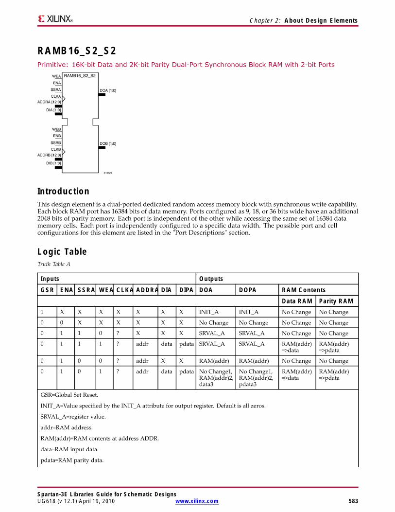
Chapter 2: About Design Elements
RAMB16_S2_S2Primitive: 16K-bit Data and 2K-bit Parity Dual-Port Synchronous Block RAM with 2-bit Ports
IntroductionThis design element is a dual-ported dedicated random access memory block with synchronous write capability.Each block RAM port has 16384 bits of data memory. Ports configured as 9, 18, or 36 bits wide have an additional2048 bits of parity memory. Each port is independent of the other while accessing the same set of 16384 datamemory cells. Each port is independently configured to a specific data width. The possible port and cellconfigurations for this element are listed in the "Port Descriptions" section.
Logic TableTruth Table A
Inputs Outputs
GSR ENA SSRA WEA CLKA ADDRA DIA DIPA DOA DOPA RAM ContentsData RAM Parity RAM
1 X X X X X X X INIT_A INIT_A No Change No Change
0 0 X X X X X X No Change No Change No Change No Change
0 1 1 0 ? X X X SRVAL_A SRVAL_A No Change No Change
0 1 1 1 ? addr data pdata SRVAL_A SRVAL_A RAM(addr)=>data
RAM(addr)=>pdata
0 1 0 0 ? addr X X RAM(addr) RAM(addr) No Change No Change
0 1 0 1 ? addr data pdata No Change1,RAM(addr)2,data3
No Change1,RAM(addr)2,pdata3
RAM(addr)=>data
RAM(addr)=>pdata
GSR=Global Set Reset.
INIT_A=Value specified by the INIT_A attribute for output register. Default is all zeros.
SRVAL_A=register value.
addr=RAM address.
RAM(addr)=RAM contents at address ADDR.
data=RAM input data.
pdata=RAM parity data.
Spartan-3E Libraries Guide for Schematic DesignsUG618 (v 12.1) April 19, 2010 www.xilinx.com 583

Chapter 2: About Design Elements
Inputs Outputs
GSR ENA SSRA WEA CLKA ADDRA DIA DIPA DOA DOPA RAM ContentsData RAM Parity RAM
1WRITE_MODE_A=NO_CHANGE.
2WRITE_MODE_A=READ_FIRST.
3WRITE_MODE_A=WRITE_FIRST.
Spartan-3E Libraries Guide for Schematic Designs584 www.xilinx.com UG618 (v 12.1) April 19, 2010

Chapter 2: About Design Elements
Truth Table B
Inputs Outputs
GSR ENB SSRB WEB CLKB ADDRB DIB DIPB DOB DOPB RAM ContentsDataRAM
ParityRAM
1 X X X X X X X INIT_B INIT_B No Change No Change
0 0 X X X X X X No Change No Change No Change No Change
0 1 1 0 ? X X X SRVAL_B SRVAL_B No Change No Change
0 1 1 1 ? addr data pdata SRVAL_B SRVAL_B RAM(addr)=>data
RAM(addr)=>pdata
0 1 0 0 ? addr X X RAM(addr) RAM(addr) No Change No Change
0 1 0 1 ? addr data pdata No Change1,RAM(addr)=>data,data3
No Change1,RAM(addr)=>data,pdata3
RAM(addr)=>data
RAM(addr)=>pdata
GSR=Global Set Reset.
INIT_B=Value specified by the INIT_B attribute for output registers. Default is all zeros.
SRVAL_B=register value.
addr=RAM address.
RAM(addr)=RAM contents at address ADDR.
data=RAM input data.
pdata=RAM parity data.
1WRITE_MODE_B=NO_CHANGE.
2WRITE_MODE_B=READ_FIRST.
3WRITE_MODE_B=WRITE_FIRST.
Port DescriptionsPort A Port BDesignElement
DataCells(a)
ParityCells(a)
AddressBus
DataBus
ParityBus
DataCells(a)
ParityCells(a)
AddressBus
DataBus
ParityBus
RAMB16_S2_S2 8192 x 2 - (12:0) (1:0) - 8192 x 2 - (12:0) (1:0) -
(a)Depth x Width
Each port is fully synchronous with independent clock pins. All Port A input pins have setup time referencedto the CLKA pin and its data output bus DOA has a clock-to-out time referenced to the CLKA. All Port Binput pins have setup time referenced to the CLKB pin and its data output bus DOB has a clock-to-out timereferenced to the CLKB. The enable ENA pin controls read, write, and reset for Port A. When ENA is Low, nodata is written and the outputs (DOA and DOPA) retain the last state. When ENA is High and reset (SSRA) isHigh, DOA and DOPA are set to SRVAL_A during the Low-to-High clock (CLKA) transition; if write enable(WEA) is High, the memory contents reflect the data at DIA and DIPA. When ENA is High and WEA is Low,the data stored in the RAM address (ADDRA) is read during the Low-to-High clock transition. By default,WRITE_MODE_A=WRITE_FIRST, when ENA and WEA are High, the data on the data inputs (DIA and DIPA) isloaded into the word selected by the write address (ADDRA) during the Low-to-High clock transition and thedata outputs (DOA and DOPA) reflect the selected (addressed) word.
Spartan-3E Libraries Guide for Schematic DesignsUG618 (v 12.1) April 19, 2010 www.xilinx.com 585
Chapter 2: About Design Elements
The enable ENB pin controls read, write, and reset for Port B. When ENB is Low, no data is written and theoutputs (DOB and DOPB) retain the last state. When ENB is High and reset (SSRB) is High, DOB and DOPB areset to SRVAL_B during the Low-to-High clock (CLKB) transition; if write enable (WEB) is High, the memorycontents reflect the data at DIB and DIPB. When ENB is High and WEB is Low, the data stored in the RAMaddress (ADDRB) is read during the Low-to-High clock transition. By default, WRITE_MODE_B=WRITE_FIRST,when ENB and WEB are High, the data on the data inputs (DIB and PB) are loaded into the word selected by thewrite address (ADDRB) during the Low-to-High clock transition and the data outputs (DOB and DOPB) reflectthe selected (addressed) word. The above descriptions assume active High control pins (ENA, WEA, SSRA,CLKA, ENB, WEB, SSRB, and CLKB). However, the active level can be changed by placing an inverter on theport. Any inverter placed on a RAMB16 port is absorbed into the block and does not use a CLB resource.
Address Mapping
Each port accesses the same set of 18432 memory cells using an addressing scheme that is dependent on thewidth of the port. For all port widths, 16384 memory cells are available for data as shown in the Port AddressMapping for Data table below. For 9-, 18-, and 36-bit wide ports, 2408 parity memory cells are also availableas shown in Port Address Mapping for Parity table below. The physical RAM location that is addressed for aparticular width is determined from the following formula.
Start=((ADDR port+1)*(Widthport)) -1
End=(ADDRport)*(Widthport)
The following tables shows address mapping for each port width.
Port Address Mapping for Data
DataWidth Port Data Addresses1 16384 <-- 31 30 29 28 27 26 25 24 23 22 21 20 19 18 17 16 15 14 13 12 11 10 9 8 7 6 5 4 3 2 1 0
2 8192 <-- 15 14 13 12 11 10 9 8 7 6 5 4 3 2 1 0
4 4096 <-- 7 6 5 4 3 2 1 0
8 2048 <-- 3 2 1 0
16 1024 <-- 1 0
32 512 <-- 0
Port Address Mapping for Parity
ParityWidth Port Parity Addresses1 2048 <----- 3 2 1 0
2 1024 <----- 1 0
4 512 <----- 0
Initializing Memory Contents of a Dual-Port RAMB16
You can use the INIT_xx attributes to specify an initialization value for the memory contents of a RAMB16 duringdevice configuration. The initialization of each RAMB16_Sm_Sn is set by 64 initialization attributes (INIT_00through INIT_3F) of 64 hex values for a total of 16384 bits.
You can use the INITP_xx attributes to specify an initial value for the parity memory during device configurationor assertion. The initialization of the parity memory for ports configured for 9, 18, or 36 bits is set by 8initialization attributes (INITP_00 through INITP_07) of 64 hex values for a total of 2048 bits.
If any INIT_xx or INITP_xx attribute is not specified, it is configured as zeros. Partial Strings are padded withzeros to the left.
Initializing the Output Register of a Dual-Port RAMB16
Spartan-3E Libraries Guide for Schematic Designs586 www.xilinx.com UG618 (v 12.1) April 19, 2010

Chapter 2: About Design Elements
In Spartan®-3A and above devices, each bit in an output register can be initialized at power on (when GSR ishigh) to either a 0 or 1. In addition, the initial state specified for power on can be different than the state thatresults from assertion of a set/reset. Four properties control initialization of the output register for a dual-portRAMB16: INIT_A, INIT_B, SRVAL_A, and SRVAL_B. The INIT_A attribute specifies the output register value atpower on for Port A and the INIT_B attribute specifies the value for Port B. You can use the SRVAL_A attribute todefine the state resulting from assertion of the SSR (set/reset) input on Port A. You can use the SRVAL_B attributeto define the state resulting from assertion of the SSR input on Port B.
The INIT_A, INIT_B, SRVAL_A, and SRVAL_B attributes specify the initialization value as a hexadecimal String.The value is dependent upon the port width. For example, for a RAMB16_S1_S4 with Port A width equal to 1and Port B width equal to 4, the Port A output register contains 1 bit and the Port B output register contains 4bits. Therefore, the INIT_A or SRVAL_A value can only be specified as a 1 or 0. For Port B, the output registercontains 4 bits. In this case, you can use INIT_B or SRVAL_B to specify a hexadecimal value from 0 through F toinitialize the 4 bits of the output register.
For those ports that include parity bits, the parity portion of the output register is specified in the high order bitposition of the INIT_A, INIT_B, SRVAL_A, or SRVAL_B value.
The INIT and SRVAL attributes default to zero if they are not set by you.
Write Mode Selection
TheWRITE_MODE_A attribute controls the memory and output contents of Port A for a dual-port RAMB16. TheWRITE_MODE_B attribute does the same for Port B. By default, both WRITE_MODE_A and WRITE_MODE_Bare set to WRITE_FIRST. This means that input is read, written to memory, and then passed to output. You canset the write mode for Port A and Port B to READ_FIRST to read the memory contents, pass the memory contentsto the outputs, and then write the input to memory. Or, you can set the write mode to NO_CHANGE to havethe input written to memory without changing the output. The Port A and Port B Conflict Resolution sectiondescribes how read/write conflicts are resolved when both Port A and Port B are attempting to read/write tothe same memory cells.
Port A and Port B Conflict Resolution
Spartan-3A block SelectRAM™ is True Dual-Port RAM that allows both ports to simultaneously access the samememory cell. When one port writes to a given memory cell, the other port must not address that memory cell (fora write or a read) within the clock-to-clock setup window.
The following tables summarize the collision detection behavior of the dual-port RAMB16 based on theWRITE_MODE_A and WRITE_MODE_B settings.
WRITE_MODE_A=NO_CHANGE and WRITE_MODE_B=NO_CHANGE
WEA WEB CLKA CLKB DIA DIB DIPA DIPB DOA DOB DOPA DOPBDataRAM
ParityRAM
0 0 ? ? DIA DIB DIPA DIPB RAM RAM RAM RAM NoChange
NoChange
1 0 ? ? DIA DIB DIPA DIPB NoChange
X NoChange
X DIA DIPA
0 1 ? ? DIA DIB DIPA DIPB X NoChange
X NoChange
DIB DIPB
1 1 ? ? DIA DIB DIPA DIPB NoChange
NoChange
NoChange
NoChange
X X
WRITE_MODE_A=READ_FIRST and WRITE_MODE_B=READ_FIRST
Spartan-3E Libraries Guide for Schematic DesignsUG618 (v 12.1) April 19, 2010 www.xilinx.com 587
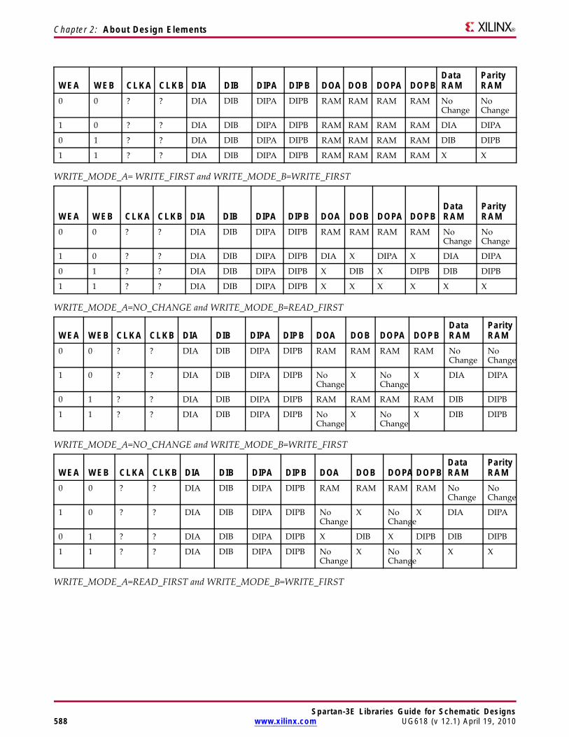
Chapter 2: About Design Elements
WEA WEB CLKA CLKB DIA DIB DIPA DIPB DOA DOB DOPA DOPBDataRAM
ParityRAM
0 0 ? ? DIA DIB DIPA DIPB RAM RAM RAM RAM NoChange
NoChange
1 0 ? ? DIA DIB DIPA DIPB RAM RAM RAM RAM DIA DIPA
0 1 ? ? DIA DIB DIPA DIPB RAM RAM RAM RAM DIB DIPB
1 1 ? ? DIA DIB DIPA DIPB RAM RAM RAM RAM X X
WRITE_MODE_A= WRITE_FIRST and WRITE_MODE_B=WRITE_FIRST
WEA WEB CLKA CLKB DIA DIB DIPA DIPB DOA DOB DOPA DOPBDataRAM
ParityRAM
0 0 ? ? DIA DIB DIPA DIPB RAM RAM RAM RAM NoChange
NoChange
1 0 ? ? DIA DIB DIPA DIPB DIA X DIPA X DIA DIPA
0 1 ? ? DIA DIB DIPA DIPB X DIB X DIPB DIB DIPB
1 1 ? ? DIA DIB DIPA DIPB X X X X X X
WRITE_MODE_A=NO_CHANGE and WRITE_MODE_B=READ_FIRST
WEA WEB CLKA CLKB DIA DIB DIPA DIPB DOA DOB DOPA DOPBDataRAM
ParityRAM
0 0 ? ? DIA DIB DIPA DIPB RAM RAM RAM RAM NoChange
NoChange
1 0 ? ? DIA DIB DIPA DIPB NoChange
X NoChange
X DIA DIPA
0 1 ? ? DIA DIB DIPA DIPB RAM RAM RAM RAM DIB DIPB
1 1 ? ? DIA DIB DIPA DIPB NoChange
X NoChange
X DIB DIPB
WRITE_MODE_A=NO_CHANGE and WRITE_MODE_B=WRITE_FIRST
WEA WEB CLKA CLKB DIA DIB DIPA DIPB DOA DOB DOPA DOPBDataRAM
ParityRAM
0 0 ? ? DIA DIB DIPA DIPB RAM RAM RAM RAM NoChange
NoChange
1 0 ? ? DIA DIB DIPA DIPB NoChange
X NoChange
X DIA DIPA
0 1 ? ? DIA DIB DIPA DIPB X DIB X DIPB DIB DIPB
1 1 ? ? DIA DIB DIPA DIPB NoChange
X NoChange
X X X
WRITE_MODE_A=READ_FIRST and WRITE_MODE_B=WRITE_FIRST
Spartan-3E Libraries Guide for Schematic Designs588 www.xilinx.com UG618 (v 12.1) April 19, 2010
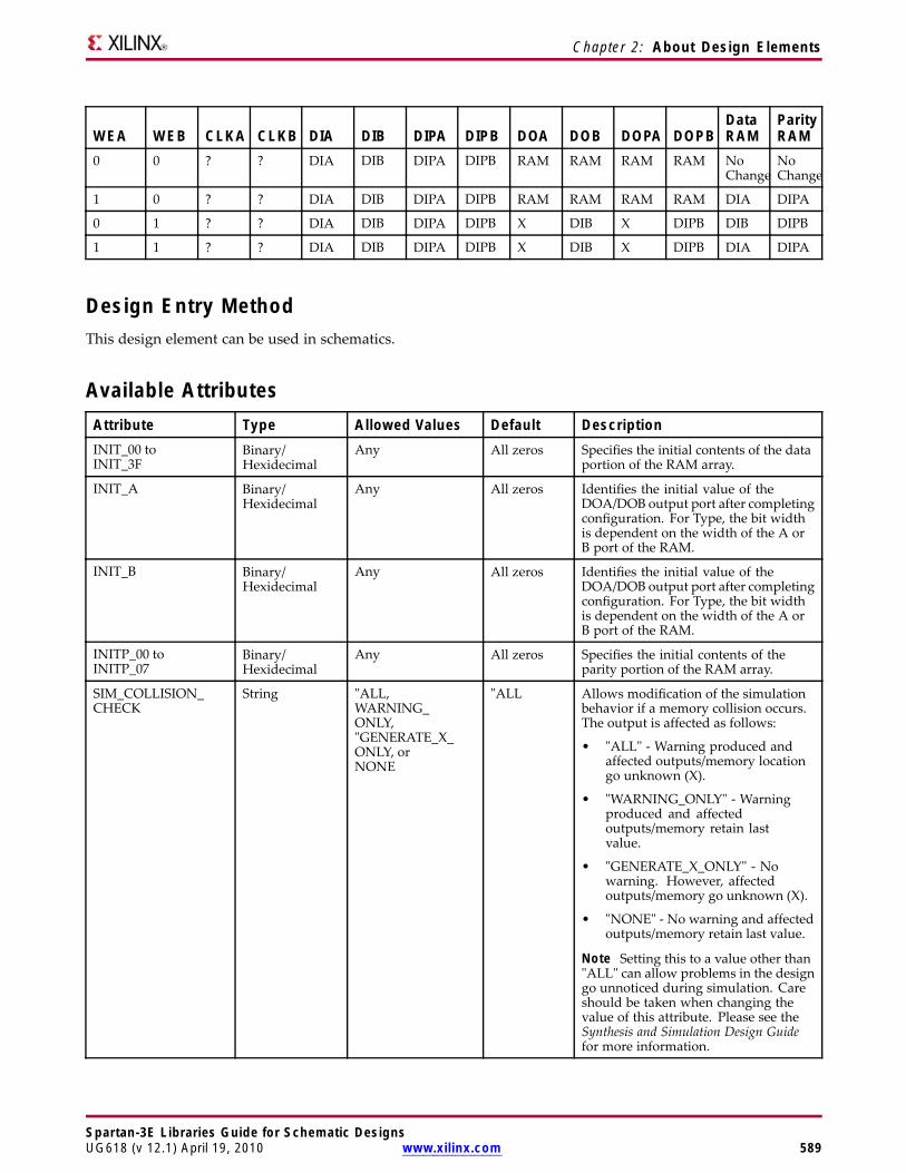
Chapter 2: About Design Elements
WEA WEB CLKA CLKB DIA DIB DIPA DIPB DOA DOB DOPA DOPBDataRAM
ParityRAM
0 0 ? ? DIA DIB DIPA DIPB RAM RAM RAM RAM NoChange
NoChange
1 0 ? ? DIA DIB DIPA DIPB RAM RAM RAM RAM DIA DIPA
0 1 ? ? DIA DIB DIPA DIPB X DIB X DIPB DIB DIPB
1 1 ? ? DIA DIB DIPA DIPB X DIB X DIPB DIA DIPA
Design Entry MethodThis design element can be used in schematics.
Available AttributesAttribute Type Allowed Values Default DescriptionINIT_00 toINIT_3F
Binary/Hexidecimal
Any All zeros Specifies the initial contents of the dataportion of the RAM array.
INIT_A Binary/Hexidecimal
Any All zeros Identifies the initial value of theDOA/DOB output port after completingconfiguration. For Type, the bit widthis dependent on the width of the A orB port of the RAM.
INIT_B Binary/Hexidecimal
Any All zeros Identifies the initial value of theDOA/DOB output port after completingconfiguration. For Type, the bit widthis dependent on the width of the A orB port of the RAM.
INITP_00 toINITP_07
Binary/Hexidecimal
Any All zeros Specifies the initial contents of theparity portion of the RAM array.
SIM_COLLISION_CHECK
String "ALL,WARNING_ONLY,"GENERATE_X_ONLY, orNONE
"ALL Allows modification of the simulationbehavior if a memory collision occurs.The output is affected as follows:
• "ALL" - Warning produced andaffected outputs/memory locationgo unknown (X).
• "WARNING_ONLY" - Warningproduced and affectedoutputs/memory retain lastvalue.
• "GENERATE_X_ONLY" - Nowarning. However, affectedoutputs/memory go unknown (X).
• "NONE" - No warning and affectedoutputs/memory retain last value.
Note Setting this to a value other than"ALL" can allow problems in the designgo unnoticed during simulation. Careshould be taken when changing thevalue of this attribute. Please see theSynthesis and Simulation Design Guidefor more information.
Spartan-3E Libraries Guide for Schematic DesignsUG618 (v 12.1) April 19, 2010 www.xilinx.com 589
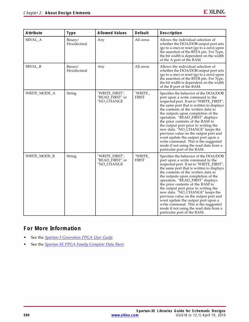
Chapter 2: About Design Elements
Attribute Type Allowed Values Default DescriptionSRVAL_A Binary/
HexidecimalAny All zeros Allows the individual selection of
whether the DOA/DOB output port sets(go to a one) or reset (go to a zero) uponthe assertion of the RSTA pin. For Type,the bit width is dependent on the widthof the A port of the RAM.
SRVAL_B Binary/Hexidecimal
Any All zeros Allows the individual selection ofwhether the DOA/DOB output port sets(go to a one) or reset (go to a zero) uponthe assertion of the RSTB pin. For Type,the bit width is dependent on the widthof the B port of the RAM.
WRITE_MODE_A String "WRITE_FIRST","READ_FIRST" or"NO_CHANGE
"WRITE_FIRST
Specifies the behavior of the DOA/DOBport upon a write command to therespected port. If set to "WRITE_FIRST",the same port that is written to displaysthe contents of the written data tothe outputs upon completion of theoperation. "READ_FIRST" displaysthe prior contents of the RAM tothe output port prior to writing thenew data. "NO_CHANGE" keeps theprevious value on the output port andwont update the output port upon awrite command. This is the suggestedmode if not using the read data from aparticular port of the RAM.
WRITE_MODE_B String "WRITE_FIRST","READ_FIRST" or"NO_CHANGE
"WRITE_FIRST
Specifies the behavior of the DOA/DOBport upon a write command to therespected port. If set to "WRITE_FIRST",the same port that is written to displaysthe contents of the written data tothe outputs upon completion of theoperation. "READ_FIRST" displaysthe prior contents of the RAM tothe output port prior to writing thenew data. "NO_CHANGE" keeps theprevious value on the output port andwont update the output port upon awrite command. This is the suggestedmode if not using the read data from aparticular port of the RAM.
For More Information• See the Spartan-3 Generation FPGA User Guide.
• See the Spartan-3E FPGA Family Complete Data Sheet.
Spartan-3E Libraries Guide for Schematic Designs590 www.xilinx.com UG618 (v 12.1) April 19, 2010

Spartan-3E Libraries Guide for Schematic Designs591 www.xilinx.com UG618 (v 12.1) April 19, 2010

Chapter 2: About Design Elements
RAMB16_S2_S36Primitive: 16K-bit Data and 2K-bit Parity Dual-Port Synchronous Block RAM with 2-bit and 36-bitPorts
IntroductionThis design element is a dual-ported dedicated random access memory block with synchronous write capability.Each block RAM port has 16384 bits of data memory. Ports configured as 9, 18, or 36 bits wide have an additional2048 bits of parity memory. Each port is independent of the other while accessing the same set of 16384 datamemory cells. Each port is independently configured to a specific data width. The possible port and cellconfigurations for this element are listed in the "Port Descriptions" section.
Logic TableTruth Table A
Inputs Outputs
GSR ENA SSRA WEA CLKA ADDRA DIA DIPA DOA DOPA RAM ContentsData RAM Parity RAM
1 X X X X X X X INIT_A INIT_A No Change No Change
0 0 X X X X X X No Change No Change No Change No Change
0 1 1 0 ? X X X SRVAL_A SRVAL_A No Change No Change
0 1 1 1 ? addr data pdata SRVAL_A SRVAL_A RAM(addr)=>data
RAM(addr)=>pdata
0 1 0 0 ? addr X X RAM(addr) RAM(addr) No Change No Change
0 1 0 1 ? addr data pdata No Change1,RAM(addr)2,data3
No Change1,RAM(addr)2,pdata3
RAM(addr)=>data
RAM(addr)=>pdata
GSR=Global Set Reset.
INIT_A=Value specified by the INIT_A attribute for output register. Default is all zeros.
SRVAL_A=register value.
addr=RAM address.
RAM(addr)=RAM contents at address ADDR.
data=RAM input data.
Spartan-3E Libraries Guide for Schematic Designs592 www.xilinx.com UG618 (v 12.1) April 19, 2010

Chapter 2: About Design Elements
Inputs Outputs
GSR ENA SSRA WEA CLKA ADDRA DIA DIPA DOA DOPA RAM ContentsData RAM Parity RAM
pdata=RAM parity data.
1WRITE_MODE_A=NO_CHANGE.
2WRITE_MODE_A=READ_FIRST.
3WRITE_MODE_A=WRITE_FIRST.
Spartan-3E Libraries Guide for Schematic DesignsUG618 (v 12.1) April 19, 2010 www.xilinx.com 593

Chapter 2: About Design Elements
Truth Table B
Inputs Outputs
GSR ENB SSRB WEB CLKB ADDRB DIB DIPB DOB DOPB RAM ContentsDataRAM
ParityRAM
1 X X X X X X X INIT_B INIT_B No Change No Change
0 0 X X X X X X No Change No Change No Change No Change
0 1 1 0 ? X X X SRVAL_B SRVAL_B No Change No Change
0 1 1 1 ? addr data pdata SRVAL_B SRVAL_B RAM(addr)=>data
RAM(addr)=>pdata
0 1 0 0 ? addr X X RAM(addr) RAM(addr) No Change No Change
0 1 0 1 ? addr data pdata No Change1,RAM(addr)=>data,data3
No Change1,RAM(addr)=>data,pdata3
RAM(addr)=>data
RAM(addr)=>pdata
GSR=Global Set Reset.
INIT_B=Value specified by the INIT_B attribute for output registers. Default is all zeros.
SRVAL_B=register value.
addr=RAM address.
RAM(addr)=RAM contents at address ADDR.
data=RAM input data.
pdata=RAM parity data.
1WRITE_MODE_B=NO_CHANGE.
2WRITE_MODE_B=READ_FIRST.
3WRITE_MODE_B=WRITE_FIRST.
Port DescriptionsPort A Port BDesignElement
DataCells(a)
ParityCells(a)
AddressBus
DataBus
ParityBus
DataCells(a)
ParityCells(a)
AddressBus
DataBus
ParityBus
RAMB16_S2_S36 8192 x 2 - (12:0) (1:0) - 512 x 32 512 x 4 (8:0) (31:0) (3:0)
(a)Depth x Width
Each port is fully synchronous with independent clock pins. All Port A input pins have setup time referencedto the CLKA pin and its data output bus DOA has a clock-to-out time referenced to the CLKA. All Port Binput pins have setup time referenced to the CLKB pin and its data output bus DOB has a clock-to-out timereferenced to the CLKB. The enable ENA pin controls read, write, and reset for Port A. When ENA is Low, nodata is written and the outputs (DOA and DOPA) retain the last state. When ENA is High and reset (SSRA) isHigh, DOA and DOPA are set to SRVAL_A during the Low-to-High clock (CLKA) transition; if write enable(WEA) is High, the memory contents reflect the data at DIA and DIPA. When ENA is High and WEA is Low,the data stored in the RAM address (ADDRA) is read during the Low-to-High clock transition. By default,WRITE_MODE_A=WRITE_FIRST, when ENA and WEA are High, the data on the data inputs (DIA and DIPA) isloaded into the word selected by the write address (ADDRA) during the Low-to-High clock transition and thedata outputs (DOA and DOPA) reflect the selected (addressed) word.
Spartan-3E Libraries Guide for Schematic Designs594 www.xilinx.com UG618 (v 12.1) April 19, 2010

Chapter 2: About Design Elements
The enable ENB pin controls read, write, and reset for Port B. When ENB is Low, no data is written and theoutputs (DOB and DOPB) retain the last state. When ENB is High and reset (SSRB) is High, DOB and DOPB areset to SRVAL_B during the Low-to-High clock (CLKB) transition; if write enable (WEB) is High, the memorycontents reflect the data at DIB and DIPB. When ENB is High and WEB is Low, the data stored in the RAMaddress (ADDRB) is read during the Low-to-High clock transition. By default, WRITE_MODE_B=WRITE_FIRST,when ENB and WEB are High, the data on the data inputs (DIB and PB) are loaded into the word selected by thewrite address (ADDRB) during the Low-to-High clock transition and the data outputs (DOB and DOPB) reflectthe selected (addressed) word. The above descriptions assume active High control pins (ENA, WEA, SSRA,CLKA, ENB, WEB, SSRB, and CLKB). However, the active level can be changed by placing an inverter on theport. Any inverter placed on a RAMB16 port is absorbed into the block and does not use a CLB resource.
Address Mapping
Each port accesses the same set of 18432 memory cells using an addressing scheme that is dependent on thewidth of the port. For all port widths, 16384 memory cells are available for data as shown in the Port AddressMapping for Data table below. For 9-, 18-, and 36-bit wide ports, 2408 parity memory cells are also availableas shown in Port Address Mapping for Parity table below. The physical RAM location that is addressed for aparticular width is determined from the following formula.
Start=((ADDR port+1)*(Widthport)) -1
End=(ADDRport)*(Widthport)
The following tables shows address mapping for each port width.
Port Address Mapping for Data
DataWidth Port Data Addresses1 16384 <-- 31 30 29 28 27 26 2524 23 22 21 20 19 18 17 16 15 14 13 12 11 10 9 8 7 6 5 4 3 2 1 0
2 8192 <-- 15 14 13 12 11 10 9 8 7 6 5 4 3 2 1 0
4 4096 <-- 7 6 5 4 3 2 1 0
8 2048 <-- 3 2 1 0
16 1024 <-- 1 0
32 512 <-- 0
Port Address Mapping for Parity
ParityWidth Port Parity Addresses1 2048 <----- 3 2 1 0
2 1024 <----- 1 0
4 512 <----- 0
Initializing Memory Contents of a Dual-Port RAMB16
You can use the INIT_xx attributes to specify an initialization value for the memory contents of a RAMB16 duringdevice configuration. The initialization of each RAMB16_Sm_Sn is set by 64 initialization attributes (INIT_00through INIT_3F) of 64 hex values for a total of 16384 bits.
You can use the INITP_xx attributes to specify an initial value for the parity memory during device configurationor assertion. The initialization of the parity memory for ports configured for 9, 18, or 36 bits is set by 8initialization attributes (INITP_00 through INITP_07) of 64 hex values for a total of 2048 bits.
If any INIT_xx or INITP_xx attribute is not specified, it is configured as zeros. Partial Strings are padded withzeros to the left.
Initializing the Output Register of a Dual-Port RAMB16
Spartan-3E Libraries Guide for Schematic DesignsUG618 (v 12.1) April 19, 2010 www.xilinx.com 595
Chapter 2: About Design Elements
In Spartan®-3A and above devices, each bit in an output register can be initialized at power on (when GSR ishigh) to either a 0 or 1. In addition, the initial state specified for power on can be different than the state thatresults from assertion of a set/reset. Four properties control initialization of the output register for a dual-portRAMB16: INIT_A, INIT_B, SRVAL_A, and SRVAL_B. The INIT_A attribute specifies the output register value atpower on for Port A and the INIT_B attribute specifies the value for Port B. You can use the SRVAL_A attribute todefine the state resulting from assertion of the SSR (set/reset) input on Port A. You can use the SRVAL_B attributeto define the state resulting from assertion of the SSR input on Port B.
The INIT_A, INIT_B, SRVAL_A, and SRVAL_B attributes specify the initialization value as a hexadecimal String.The value is dependent upon the port width. For example, for a RAMB16_S1_S4 with Port A width equal to 1and Port B width equal to 4, the Port A output register contains 1 bit and the Port B output register contains 4bits. Therefore, the INIT_A or SRVAL_A value can only be specified as a 1 or 0. For Port B, the output registercontains 4 bits. In this case, you can use INIT_B or SRVAL_B to specify a hexadecimal value from 0 through F toinitialize the 4 bits of the output register.
For those ports that include parity bits, the parity portion of the output register is specified in the high order bitposition of the INIT_A, INIT_B, SRVAL_A, or SRVAL_B value.
The INIT and SRVAL attributes default to zero if they are not set by you.
Write Mode Selection
TheWRITE_MODE_A attribute controls the memory and output contents of Port A for a dual-port RAMB16. TheWRITE_MODE_B attribute does the same for Port B. By default, both WRITE_MODE_A and WRITE_MODE_Bare set to WRITE_FIRST. This means that input is read, written to memory, and then passed to output. You canset the write mode for Port A and Port B to READ_FIRST to read the memory contents, pass the memory contentsto the outputs, and then write the input to memory. Or, you can set the write mode to NO_CHANGE to havethe input written to memory without changing the output. The Port A and Port B Conflict Resolution sectiondescribes how read/write conflicts are resolved when both Port A and Port B are attempting to read/write tothe same memory cells.
Port A and Port B Conflict Resolution
Spartan-3A block SelectRAM™ is True Dual-Port RAM that allows both ports to simultaneously access the samememory cell. When one port writes to a given memory cell, the other port must not address that memory cell (fora write or a read) within the clock-to-clock setup window.
The following tables summarize the collision detection behavior of the dual-port RAMB16 based on theWRITE_MODE_A and WRITE_MODE_B settings.
WRITE_MODE_A=NO_CHANGE and WRITE_MODE_B=NO_CHANGE
WEA WEB CLKA CLKB DIA DIB DIPA DIPB DOA DOB DOPA DOPBDataRAM
ParityRAM
0 0 ? ? DIA DIB DIPA DIPB RAM RAM RAM RAM NoChange
NoChange
1 0 ? ? DIA DIB DIPA DIPB NoChange
X NoChange
X DIA DIPA
0 1 ? ? DIA DIB DIPA DIPB X NoChange
X NoChange
DIB DIPB
1 1 ? ? DIA DIB DIPA DIPB NoChange
NoChange
NoChange
NoChange
X X
WRITE_MODE_A=READ_FIRST and WRITE_MODE_B=READ_FIRST
Spartan-3E Libraries Guide for Schematic Designs596 www.xilinx.com UG618 (v 12.1) April 19, 2010

Chapter 2: About Design Elements
WEA WEB CLKA CLKB DIA DIB DIPA DIPB DOA DOB DOPA DOPBDataRAM
ParityRAM
0 0 ? ? DIA DIB DIPA DIPB RAM RAM RAM RAM NoChange
NoChange
1 0 ? ? DIA DIB DIPA DIPB RAM RAM RAM RAM DIA DIPA
0 1 ? ? DIA DIB DIPA DIPB RAM RAM RAM RAM DIB DIPB
1 1 ? ? DIA DIB DIPA DIPB RAM RAM RAM RAM X X
WRITE_MODE_A= WRITE_FIRST and WRITE_MODE_B=WRITE_FIRST
WEA WEB CLKA CLKB DIA DIB DIPA DIPB DOA DOB DOPA DOPBDataRAM
ParityRAM
0 0 ? ? DIA DIB DIPA DIPB RAM RAM RAM RAM NoChange
NoChange
1 0 ? ? DIA DIB DIPA DIPB DIA X DIPA X DIA DIPA
0 1 ? ? DIA DIB DIPA DIPB X DIB X DIPB DIB DIPB
1 1 ? ? DIA DIB DIPA DIPB X X X X X X
WRITE_MODE_A=NO_CHANGE and WRITE_MODE_B=READ_FIRST
WEA WEB CLKA CLKB DIA DIB DIPA DIPB DOA DOB DOPA DOPBDataRAM
ParityRAM
0 0 ? ? DIA DIB DIPA DIPB RAM RAM RAM RAM NoChange
NoChange
1 0 ? ? DIA DIB DIPA DIPB NoChange
X NoChange
X DIA DIPA
0 1 ? ? DIA DIB DIPA DIPB RAM RAM RAM RAM DIB DIPB
1 1 ? ? DIA DIB DIPA DIPB NoChange
X NoChange
X DIB DIPB
WRITE_MODE_A=NO_CHANGE and WRITE_MODE_B=WRITE_FIRST
WEA WEB CLKA CLKB DIA DIB DIPA DIPB DOA DOB DOPA DOPBDataRAM
ParityRAM
0 0 ? ? DIA DIB DIPA DIPB RAM RAM RAM RAM NoChange
NoChange
1 0 ? ? DIA DIB DIPA DIPB NoChange
X NoChange
X DIA DIPA
0 1 ? ? DIA DIB DIPA DIPB X DIB X DIPB DIB DIPB
1 1 ? ? DIA DIB DIPA DIPB NoChange
X NoChange
X X X
WRITE_MODE_A=READ_FIRST and WRITE_MODE_B=WRITE_FIRST
WEA WEB CLKA CLKB DIA DIB DIPA DIPB DOA DOB DOPA DOPBDataRAM
ParityRAM
0 0 ? ? DIA DIB DIPA DIPB RAM RAM RAM RAM NoChange
NoChange
1 0 ? ? DIA DIB DIPA DIPB RAM RAM RAM RAM DIA DIPA
0 1 ? ? DIA DIB DIPA DIPB X DIB X DIPB DIB DIPB
1 1 ? ? DIA DIB DIPA DIPB X DIB X DIPB DIA DIPA
Spartan-3E Libraries Guide for Schematic DesignsUG618 (v 12.1) April 19, 2010 www.xilinx.com 597

Chapter 2: About Design Elements
Design Entry MethodThis design element can be used in schematics.
Available Attributes
Attribute TypeAllowedValues Default Description
INIT_00 toINIT_3F
Binary/Hexadecimal
Any All zeros Specifies the initial contents of the data portionof the RAM array.
INIT_A Binary/Hexadecimal
Any All zeros Identifies the initial value of the DOA/DOB outputport after completing configuration. For Type, thebit width is dependent on the width of the A or Bport of the RAM.
INIT_B Binary/Hexadecimal
Any All zeros Identifies the initial value of the DOA/DOB outputport after completing configuration. For Type, thebit width is dependent on the width of the A or Bport of the RAM.
INITP_00 toINITP_07
Binary/Hexadecimal
Any All zeros Specifies the initial contents of the parity portionof the RAM array.
SIM_COLLISION_CHECK
String "ALL,WARNING_ONLY,"GENERATE_X_ONLY,NONE
"ALL Allows modification of the simulation behavior ifa memory collision occurs. The output is affectedas follows:
• "ALL" - Warning produced and affectedoutputs/memory location go unknown (X).
• "WARNING_ONLY" - Warning produced andaffected outputs/memory retain last value.
• "GENERATE_X_ONLY" - No warning.However, affected outputs/memory gounknown (X).
• "NONE" - No warning and affectedoutputs/memory retain last value.
Note Setting this to a value other than "ALL" canallow problems in the design go unnoticed duringsimulation. Care should be taken when changingthe value of this attribute. Please see the Synthesisand Simulation Design Guide for more information.
SRVAL_A Binary/Hexadecimal
Any All zeros Allows the individual selection of whether theDOA/DOB output port sets (go to a one) or reset(go to a zero) upon the assertion of the RSTA pin.For Type, the bit width is dependent on the widthof the A port of the RAM.
SRVAL_B Binary/Hexadecimal
Any All zeros Allows the individual selection of whether theDOA/DOB output port sets (go to a one) or reset(go to a zero) upon the assertion of the RSTB pin.For Type, the bit width is dependent on the widthof the B port of the RAM.
Spartan-3E Libraries Guide for Schematic Designs598 www.xilinx.com UG618 (v 12.1) April 19, 2010

Chapter 2: About Design Elements
Attribute TypeAllowedValues Default Description
WRITE_MODE_A String "WRITE_FIRST","READ_FIRST","NO_CHANGE
"WRITE_FIRST
Specifies the behavior of the DOA/DOB port upona write command to the respected port. If set to"WRITE_FIRST", the same port that is writtento displays the contents of the written data tothe outputs upon completion of the operation."READ_FIRST" displays the prior contents of theRAM to the output port prior to writing the newdata. "NO_CHANGE" keeps the previous valueon the output port and wont update the outputport upon a write command. This is the suggestedmode if not using the read data from a particularport of the RAM.
WRITE_MODE_B String "WRITE_FIRST","READ_FIRST","NO_CHANGE
"WRITE_FIRST
Specifies the behavior of the DOA/DOB port upona write command to the respected port. If set to"WRITE_FIRST", the same port that is writtento displays the contents of the written data tothe outputs upon completion of the operation."READ_FIRST" displays the prior contents of theRAM to the output port prior to writing the newdata. "NO_CHANGE" keeps the previous valueon the output port and wont update the outputport upon a write command. This is the suggestedmode if not using the read data from a particularport of the RAM.
For More Information• See the Spartan-3 Generation FPGA User Guide.
• See the Spartan-3E FPGA Family Complete Data Sheet.
Spartan-3E Libraries Guide for Schematic DesignsUG618 (v 12.1) April 19, 2010 www.xilinx.com 599

Spartan-3E Libraries Guide for Schematic Designs600 www.xilinx.com UG618 (v 12.1) April 19, 2010
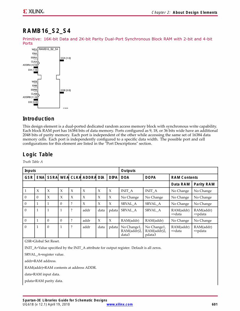
Chapter 2: About Design Elements
RAMB16_S2_S4Primitive: 16K-bit Data and 2K-bit Parity Dual-Port Synchronous Block RAM with 2-bit and 4-bitPorts
IntroductionThis design element is a dual-ported dedicated random access memory block with synchronous write capability.Each block RAM port has 16384 bits of data memory. Ports configured as 9, 18, or 36 bits wide have an additional2048 bits of parity memory. Each port is independent of the other while accessing the same set of 16384 datamemory cells. Each port is independently configured to a specific data width. The possible port and cellconfigurations for this element are listed in the "Port Descriptions" section.
Logic TableTruth Table A
Inputs Outputs
GSR ENA SSRA WEA CLKA ADDRA DIA DIPA DOA DOPA RAM ContentsData RAM Parity RAM
1 X X X X X X X INIT_A INIT_A No Change No Change
0 0 X X X X X X No Change No Change No Change No Change
0 1 1 0 ? X X X SRVAL_A SRVAL_A No Change No Change
0 1 1 1 ? addr data pdata SRVAL_A SRVAL_A RAM(addr)=>data
RAM(addr)=>pdata
0 1 0 0 ? addr X X RAM(addr) RAM(addr) No Change No Change
0 1 0 1 ? addr data pdata No Change1,RAM(addr)2,data3
No Change1,RAM(addr)2,pdata3
RAM(addr)=>data
RAM(addr)=>pdata
GSR=Global Set Reset.
INIT_A=Value specified by the INIT_A attribute for output register. Default is all zeros.
SRVAL_A=register value.
addr=RAM address.
RAM(addr)=RAM contents at address ADDR.
data=RAM input data.
pdata=RAM parity data.
Spartan-3E Libraries Guide for Schematic DesignsUG618 (v 12.1) April 19, 2010 www.xilinx.com 601

Chapter 2: About Design Elements
Inputs Outputs
GSR ENA SSRA WEA CLKA ADDRA DIA DIPA DOA DOPA RAM ContentsData RAM Parity RAM
1WRITE_MODE_A=NO_CHANGE.
2WRITE_MODE_A=READ_FIRST.
3WRITE_MODE_A=WRITE_FIRST.
Spartan-3E Libraries Guide for Schematic Designs602 www.xilinx.com UG618 (v 12.1) April 19, 2010

Chapter 2: About Design Elements
Truth Table B
Inputs Outputs
GSR ENB SSRB WEB CLKB ADDRB DIB DIPB DOB DOPB RAM ContentsDataRAM
ParityRAM
1 X X X X X X X INIT_B INIT_B No Change No Change
0 0 X X X X X X No Change No Change No Change No Change
0 1 1 0 ? X X X SRVAL_B SRVAL_B No Change No Change
0 1 1 1 ? addr data pdata SRVAL_B SRVAL_B RAM(addr)=>data
RAM(addr)=>pdata
0 1 0 0 ? addr X X RAM(addr) RAM(addr) No Change No Change
0 1 0 1 ? addr data pdata No Change1,RAM(addr)=>data,data3
No Change1,RAM(addr)=>data,pdata3
RAM(addr)=>data
RAM(addr)=>pdata
GSR=Global Set Reset.
INIT_B=Value specified by the INIT_B attribute for output registers. Default is all zeros.
SRVAL_B=register value.
addr=RAM address.
RAM(addr)=RAM contents at address ADDR.
data=RAM input data.
pdata=RAM parity data.
1WRITE_MODE_B=NO_CHANGE.
2WRITE_MODE_B=READ_FIRST.
3WRITE_MODE_B=WRITE_FIRST.
Port DescriptionsPort A Port B
DesignElement
DataCells(a)
ParityCells(a)
AddressBus
DataBus
ParityBus
DataCells(a)
ParityCells(a)
AddressBus
DataBus
ParityBus
RAMB16_S2_S4 8192 x 2 - (12:0) (1:0) - 4096 x 4 - (11:0) (3:0) -
(a) Depth x Width
Each port is fully synchronous with independent clock pins. All Port A input pins have setup time referencedto the CLKA pin and its data output bus DOA has a clock-to-out time referenced to the CLKA. All Port Binput pins have setup time referenced to the CLKB pin and its data output bus DOB has a clock-to-out timereferenced to the CLKB. The enable ENA pin controls read, write, and reset for Port A. When ENA is Low, nodata is written and the outputs (DOA and DOPA) retain the last state. When ENA is High and reset (SSRA) isHigh, DOA and DOPA are set to SRVAL_A during the Low-to-High clock (CLKA) transition; if write enable(WEA) is High, the memory contents reflect the data at DIA and DIPA. When ENA is High and WEA is Low,the data stored in the RAM address (ADDRA) is read during the Low-to-High clock transition. By default,WRITE_MODE_A=WRITE_FIRST, when ENA and WEA are High, the data on the data inputs (DIA and DIPA) isloaded into the word selected by the write address (ADDRA) during the Low-to-High clock transition and thedata outputs (DOA and DOPA) reflect the selected (addressed) word.
Spartan-3E Libraries Guide for Schematic DesignsUG618 (v 12.1) April 19, 2010 www.xilinx.com 603
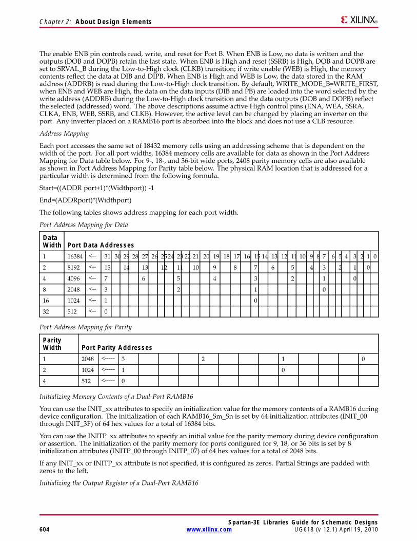
Chapter 2: About Design Elements
The enable ENB pin controls read, write, and reset for Port B. When ENB is Low, no data is written and theoutputs (DOB and DOPB) retain the last state. When ENB is High and reset (SSRB) is High, DOB and DOPB areset to SRVAL_B during the Low-to-High clock (CLKB) transition; if write enable (WEB) is High, the memorycontents reflect the data at DIB and DIPB. When ENB is High and WEB is Low, the data stored in the RAMaddress (ADDRB) is read during the Low-to-High clock transition. By default, WRITE_MODE_B=WRITE_FIRST,when ENB and WEB are High, the data on the data inputs (DIB and PB) are loaded into the word selected by thewrite address (ADDRB) during the Low-to-High clock transition and the data outputs (DOB and DOPB) reflectthe selected (addressed) word. The above descriptions assume active High control pins (ENA, WEA, SSRA,CLKA, ENB, WEB, SSRB, and CLKB). However, the active level can be changed by placing an inverter on theport. Any inverter placed on a RAMB16 port is absorbed into the block and does not use a CLB resource.
Address Mapping
Each port accesses the same set of 18432 memory cells using an addressing scheme that is dependent on thewidth of the port. For all port widths, 16384 memory cells are available for data as shown in the Port AddressMapping for Data table below. For 9-, 18-, and 36-bit wide ports, 2408 parity memory cells are also availableas shown in Port Address Mapping for Parity table below. The physical RAM location that is addressed for aparticular width is determined from the following formula.
Start=((ADDR port+1)*(Widthport)) -1
End=(ADDRport)*(Widthport)
The following tables shows address mapping for each port width.
Port Address Mapping for Data
DataWidth Port Data Addresses1 16384 <-- 31 30 29 28 27 26 2524 23 22 21 20 19 18 17 16 15 14 13 12 11 10 9 8 7 6 5 4 3 2 1 0
2 8192 <-- 15 14 13 12 11 10 9 8 7 6 5 4 3 2 1 0
4 4096 <-- 7 6 5 4 3 2 1 0
8 2048 <-- 3 2 1 0
16 1024 <-- 1 0
32 512 <-- 0
Port Address Mapping for Parity
ParityWidth Port Parity Addresses1 2048 <----- 3 2 1 0
2 1024 <----- 1 0
4 512 <----- 0
Initializing Memory Contents of a Dual-Port RAMB16
You can use the INIT_xx attributes to specify an initialization value for the memory contents of a RAMB16 duringdevice configuration. The initialization of each RAMB16_Sm_Sn is set by 64 initialization attributes (INIT_00through INIT_3F) of 64 hex values for a total of 16384 bits.
You can use the INITP_xx attributes to specify an initial value for the parity memory during device configurationor assertion. The initialization of the parity memory for ports configured for 9, 18, or 36 bits is set by 8initialization attributes (INITP_00 through INITP_07) of 64 hex values for a total of 2048 bits.
If any INIT_xx or INITP_xx attribute is not specified, it is configured as zeros. Partial Strings are padded withzeros to the left.
Initializing the Output Register of a Dual-Port RAMB16
Spartan-3E Libraries Guide for Schematic Designs604 www.xilinx.com UG618 (v 12.1) April 19, 2010

Chapter 2: About Design Elements
In Spartan®-3A and above devices, each bit in an output register can be initialized at power on (when GSR ishigh) to either a 0 or 1. In addition, the initial state specified for power on can be different than the state thatresults from assertion of a set/reset. Four properties control initialization of the output register for a dual-portRAMB16: INIT_A, INIT_B, SRVAL_A, and SRVAL_B. The INIT_A attribute specifies the output register value atpower on for Port A and the INIT_B attribute specifies the value for Port B. You can use the SRVAL_A attribute todefine the state resulting from assertion of the SSR (set/reset) input on Port A. You can use the SRVAL_B attributeto define the state resulting from assertion of the SSR input on Port B.
The INIT_A, INIT_B, SRVAL_A, and SRVAL_B attributes specify the initialization value as a hexadecimal String.The value is dependent upon the port width. For example, for a RAMB16_S1_S4 with Port A width equal to 1and Port B width equal to 4, the Port A output register contains 1 bit and the Port B output register contains 4bits. Therefore, the INIT_A or SRVAL_A value can only be specified as a 1 or 0. For Port B, the output registercontains 4 bits. In this case, you can use INIT_B or SRVAL_B to specify a hexadecimal value from 0 through F toinitialize the 4 bits of the output register.
For those ports that include parity bits, the parity portion of the output register is specified in the high order bitposition of the INIT_A, INIT_B, SRVAL_A, or SRVAL_B value.
The INIT and SRVAL attributes default to zero if they are not set by you.
Write Mode Selection
TheWRITE_MODE_A attribute controls the memory and output contents of Port A for a dual-port RAMB16. TheWRITE_MODE_B attribute does the same for Port B. By default, both WRITE_MODE_A and WRITE_MODE_Bare set to WRITE_FIRST. This means that input is read, written to memory, and then passed to output. You canset the write mode for Port A and Port B to READ_FIRST to read the memory contents, pass the memory contentsto the outputs, and then write the input to memory. Or, you can set the write mode to NO_CHANGE to havethe input written to memory without changing the output. The Port A and Port B Conflict Resolution sectiondescribes how read/write conflicts are resolved when both Port A and Port B are attempting to read/write tothe same memory cells.
Port A and Port B Conflict Resolution
Spartan-3A block SelectRAM™ is True Dual-Port RAM that allows both ports to simultaneously access the samememory cell. When one port writes to a given memory cell, the other port must not address that memory cell (fora write or a read) within the clock-to-clock setup window.
The following tables summarize the collision detection behavior of the dual-port RAMB16 based on theWRITE_MODE_A and WRITE_MODE_B settings.
WRITE_MODE_A=NO_CHANGE and WRITE_MODE_B=NO_CHANGE
WEA WEB CLKA CLKB DIA DIB DIPA DIPB DOA DOB DOPA DOPBDataRAM
ParityRAM
0 0 ? ? DIA DIB DIPA DIPB RAM RAM RAM RAM NoChange
NoChange
1 0 ? ? DIA DIB DIPA DIPB NoChange
X NoChange
X DIA DIPA
0 1 ? ? DIA DIB DIPA DIPB X NoChange
X NoChange
DIB DIPB
1 1 ? ? DIA DIB DIPA DIPB NoChange
NoChange
NoChange
NoChange
X X
WRITE_MODE_A=READ_FIRST and WRITE_MODE_B=READ_FIRST
Spartan-3E Libraries Guide for Schematic DesignsUG618 (v 12.1) April 19, 2010 www.xilinx.com 605
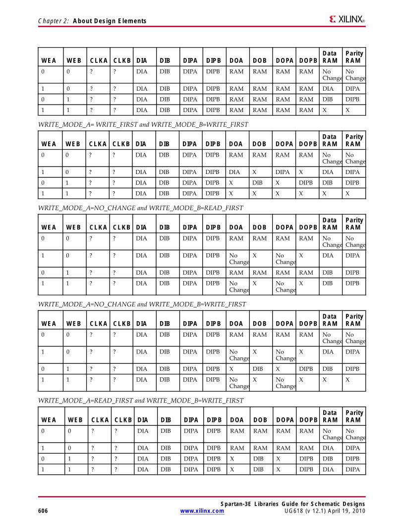
Chapter 2: About Design Elements
WEA WEB CLKA CLKB DIA DIB DIPA DIPB DOA DOB DOPA DOPBDataRAM
ParityRAM
0 0 ? ? DIA DIB DIPA DIPB RAM RAM RAM RAM NoChange
NoChange
1 0 ? ? DIA DIB DIPA DIPB RAM RAM RAM RAM DIA DIPA
0 1 ? ? DIA DIB DIPA DIPB RAM RAM RAM RAM DIB DIPB
1 1 ? ? DIA DIB DIPA DIPB RAM RAM RAM RAM X X
WRITE_MODE_A= WRITE_FIRST and WRITE_MODE_B=WRITE_FIRST
WEA WEB CLKA CLKB DIA DIB DIPA DIPB DOA DOB DOPA DOPBDataRAM
ParityRAM
0 0 ? ? DIA DIB DIPA DIPB RAM RAM RAM RAM NoChange
NoChange
1 0 ? ? DIA DIB DIPA DIPB DIA X DIPA X DIA DIPA
0 1 ? ? DIA DIB DIPA DIPB X DIB X DIPB DIB DIPB
1 1 ? ? DIA DIB DIPA DIPB X X X X X X
WRITE_MODE_A=NO_CHANGE and WRITE_MODE_B=READ_FIRST
WEA WEB CLKA CLKB DIA DIB DIPA DIPB DOA DOB DOPA DOPBDataRAM
ParityRAM
0 0 ? ? DIA DIB DIPA DIPB RAM RAM RAM RAM NoChange
NoChange
1 0 ? ? DIA DIB DIPA DIPB NoChange
X NoChange
X DIA DIPA
0 1 ? ? DIA DIB DIPA DIPB RAM RAM RAM RAM DIB DIPB
1 1 ? ? DIA DIB DIPA DIPB NoChange
X NoChange
X DIB DIPB
WRITE_MODE_A=NO_CHANGE and WRITE_MODE_B=WRITE_FIRST
WEA WEB CLKA CLKB DIA DIB DIPA DIPB DOA DOB DOPA DOPBDataRAM
ParityRAM
0 0 ? ? DIA DIB DIPA DIPB RAM RAM RAM RAM NoChange
NoChange
1 0 ? ? DIA DIB DIPA DIPB NoChange
X NoChange
X DIA DIPA
0 1 ? ? DIA DIB DIPA DIPB X DIB X DIPB DIB DIPB
1 1 ? ? DIA DIB DIPA DIPB NoChange
X NoChange
X X X
WRITE_MODE_A=READ_FIRST and WRITE_MODE_B=WRITE_FIRST
WEA WEB CLKA CLKB DIA DIB DIPA DIPB DOA DOB DOPA DOPBDataRAM
ParityRAM
0 0 ? ? DIA DIB DIPA DIPB RAM RAM RAM RAM NoChange
NoChange
1 0 ? ? DIA DIB DIPA DIPB RAM RAM RAM RAM DIA DIPA
0 1 ? ? DIA DIB DIPA DIPB X DIB X DIPB DIB DIPB
1 1 ? ? DIA DIB DIPA DIPB X DIB X DIPB DIA DIPA
Spartan-3E Libraries Guide for Schematic Designs606 www.xilinx.com UG618 (v 12.1) April 19, 2010
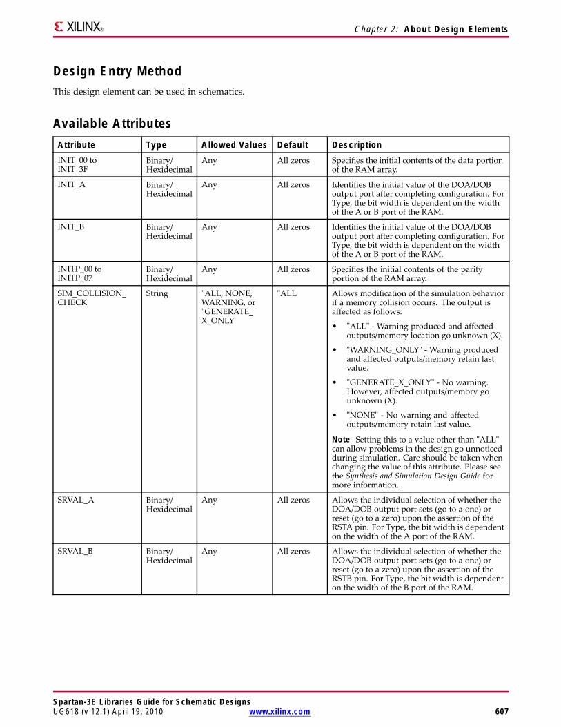
Chapter 2: About Design Elements
Design Entry MethodThis design element can be used in schematics.
Available AttributesAttribute Type Allowed Values Default DescriptionINIT_00 toINIT_3F
Binary/Hexidecimal
Any All zeros Specifies the initial contents of the data portionof the RAM array.
INIT_A Binary/Hexidecimal
Any All zeros Identifies the initial value of the DOA/DOBoutput port after completing configuration. ForType, the bit width is dependent on the widthof the A or B port of the RAM.
INIT_B Binary/Hexidecimal
Any All zeros Identifies the initial value of the DOA/DOBoutput port after completing configuration. ForType, the bit width is dependent on the widthof the A or B port of the RAM.
INITP_00 toINITP_07
Binary/Hexidecimal
Any All zeros Specifies the initial contents of the parityportion of the RAM array.
SIM_COLLISION_CHECK
String "ALL, NONE,WARNING, or"GENERATE_X_ONLY
"ALL Allows modification of the simulation behaviorif a memory collision occurs. The output isaffected as follows:
• "ALL" - Warning produced and affectedoutputs/memory location go unknown (X).
• "WARNING_ONLY" - Warning producedand affected outputs/memory retain lastvalue.
• "GENERATE_X_ONLY" - No warning.However, affected outputs/memory gounknown (X).
• "NONE" - No warning and affectedoutputs/memory retain last value.
Note Setting this to a value other than "ALL"can allow problems in the design go unnoticedduring simulation. Care should be taken whenchanging the value of this attribute. Please seethe Synthesis and Simulation Design Guide formore information.
SRVAL_A Binary/Hexidecimal
Any All zeros Allows the individual selection of whether theDOA/DOB output port sets (go to a one) orreset (go to a zero) upon the assertion of theRSTA pin. For Type, the bit width is dependenton the width of the A port of the RAM.
SRVAL_B Binary/Hexidecimal
Any All zeros Allows the individual selection of whether theDOA/DOB output port sets (go to a one) orreset (go to a zero) upon the assertion of theRSTB pin. For Type, the bit width is dependenton the width of the B port of the RAM.
Spartan-3E Libraries Guide for Schematic DesignsUG618 (v 12.1) April 19, 2010 www.xilinx.com 607
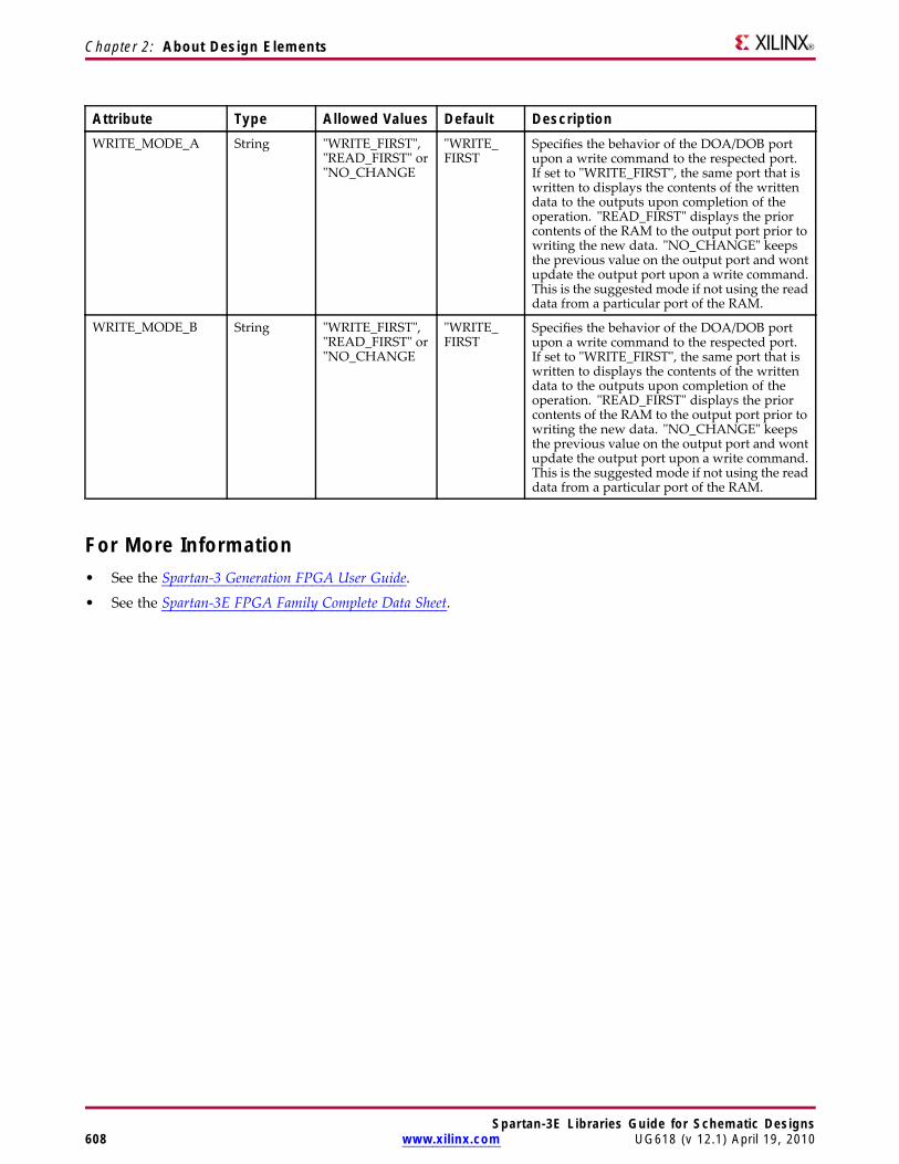
Chapter 2: About Design Elements
Attribute Type Allowed Values Default DescriptionWRITE_MODE_A String "WRITE_FIRST",
"READ_FIRST" or"NO_CHANGE
"WRITE_FIRST
Specifies the behavior of the DOA/DOB portupon a write command to the respected port.If set to "WRITE_FIRST", the same port that iswritten to displays the contents of the writtendata to the outputs upon completion of theoperation. "READ_FIRST" displays the priorcontents of the RAM to the output port prior towriting the new data. "NO_CHANGE" keepsthe previous value on the output port and wontupdate the output port upon a write command.This is the suggested mode if not using the readdata from a particular port of the RAM.
WRITE_MODE_B String "WRITE_FIRST","READ_FIRST" or"NO_CHANGE
"WRITE_FIRST
Specifies the behavior of the DOA/DOB portupon a write command to the respected port.If set to "WRITE_FIRST", the same port that iswritten to displays the contents of the writtendata to the outputs upon completion of theoperation. "READ_FIRST" displays the priorcontents of the RAM to the output port prior towriting the new data. "NO_CHANGE" keepsthe previous value on the output port and wontupdate the output port upon a write command.This is the suggested mode if not using the readdata from a particular port of the RAM.
For More Information• See the Spartan-3 Generation FPGA User Guide.
• See the Spartan-3E FPGA Family Complete Data Sheet.
Spartan-3E Libraries Guide for Schematic Designs608 www.xilinx.com UG618 (v 12.1) April 19, 2010
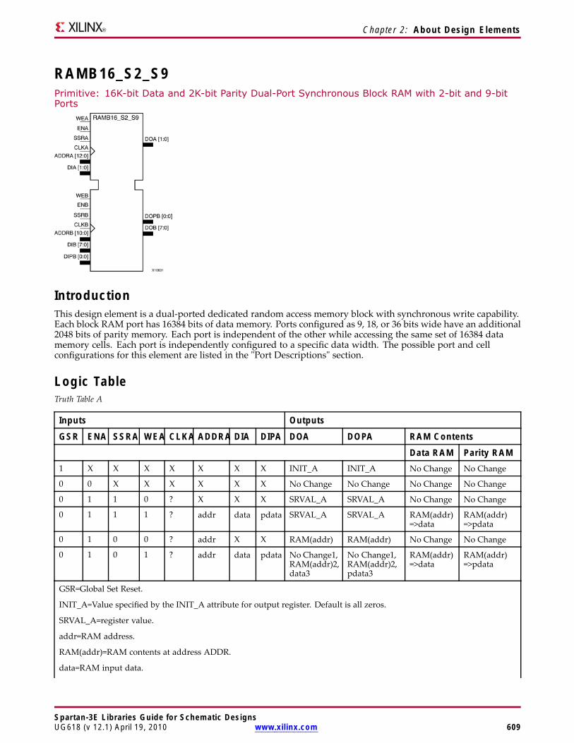
Chapter 2: About Design Elements
RAMB16_S2_S9Primitive: 16K-bit Data and 2K-bit Parity Dual-Port Synchronous Block RAM with 2-bit and 9-bitPorts
IntroductionThis design element is a dual-ported dedicated random access memory block with synchronous write capability.Each block RAM port has 16384 bits of data memory. Ports configured as 9, 18, or 36 bits wide have an additional2048 bits of parity memory. Each port is independent of the other while accessing the same set of 16384 datamemory cells. Each port is independently configured to a specific data width. The possible port and cellconfigurations for this element are listed in the "Port Descriptions" section.
Logic TableTruth Table A
Inputs Outputs
GSR ENA SSRA WEA CLKA ADDRA DIA DIPA DOA DOPA RAM ContentsData RAM Parity RAM
1 X X X X X X X INIT_A INIT_A No Change No Change
0 0 X X X X X X No Change No Change No Change No Change
0 1 1 0 ? X X X SRVAL_A SRVAL_A No Change No Change
0 1 1 1 ? addr data pdata SRVAL_A SRVAL_A RAM(addr)=>data
RAM(addr)=>pdata
0 1 0 0 ? addr X X RAM(addr) RAM(addr) No Change No Change
0 1 0 1 ? addr data pdata No Change1,RAM(addr)2,data3
No Change1,RAM(addr)2,pdata3
RAM(addr)=>data
RAM(addr)=>pdata
GSR=Global Set Reset.
INIT_A=Value specified by the INIT_A attribute for output register. Default is all zeros.
SRVAL_A=register value.
addr=RAM address.
RAM(addr)=RAM contents at address ADDR.
data=RAM input data.
Spartan-3E Libraries Guide for Schematic DesignsUG618 (v 12.1) April 19, 2010 www.xilinx.com 609
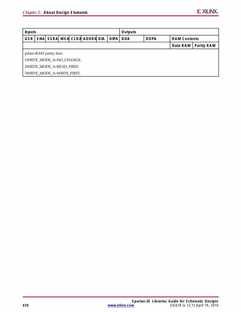
Chapter 2: About Design Elements
Inputs Outputs
GSR ENA SSRA WEA CLKA ADDRA DIA DIPA DOA DOPA RAM ContentsData RAM Parity RAM
pdata=RAM parity data.
1WRITE_MODE_A=NO_CHANGE.
2WRITE_MODE_A=READ_FIRST.
3WRITE_MODE_A=WRITE_FIRST.
Spartan-3E Libraries Guide for Schematic Designs610 www.xilinx.com UG618 (v 12.1) April 19, 2010

Chapter 2: About Design Elements
Truth Table B
Inputs Outputs
GSR ENB SSRB WEB CLKB ADDRB DIB DIPB DOB DOPB RAM ContentsDataRAM
ParityRAM
1 X X X X X X X INIT_B INIT_B No Change No Change
0 0 X X X X X X No Change No Change No Change No Change
0 1 1 0 ? X X X SRVAL_B SRVAL_B No Change No Change
0 1 1 1 ? addr data pdata SRVAL_B SRVAL_B RAM(addr)=>data
RAM(addr)=>pdata
0 1 0 0 ? addr X X RAM(addr) RAM(addr) No Change No Change
0 1 0 1 ? addr data pdata No Change1,RAM(addr)=>data,data3
No Change1,RAM(addr)=>data,pdata3
RAM(addr)=>data
RAM(addr)=>pdata
GSR=Global Set Reset.
INIT_B=Value specified by the INIT_B attribute for output registers. Default is all zeros.
SRVAL_B=register value.
addr=RAM address.
RAM(addr)=RAM contents at address ADDR.
data=RAM input data.
pdata=RAM parity data.
1WRITE_MODE_B=NO_CHANGE.
2WRITE_MODE_B=READ_FIRST.
3WRITE_MODE_B=WRITE_FIRST.
Port DescriptionsPort A Port BDesignElement
DataCells(a)
ParityCells(a)
AddressBus
DataBus
ParityBus
DataCells(a)
ParityCells(a)
AddressBus
DataBus
ParityBus
RAMB16_S2_S9 8192 x 2 - (12:0) (1:0) - 2048 x 8 2048 x 1 (10:0) (7:0) (0:0)
(a)Depth x Width
Each port is fully synchronous with independent clock pins. All Port A input pins have setup time referencedto the CLKA pin and its data output bus DOA has a clock-to-out time referenced to the CLKA. All Port Binput pins have setup time referenced to the CLKB pin and its data output bus DOB has a clock-to-out timereferenced to the CLKB. The enable ENA pin controls read, write, and reset for Port A. When ENA is Low, nodata is written and the outputs (DOA and DOPA) retain the last state. When ENA is High and reset (SSRA) isHigh, DOA and DOPA are set to SRVAL_A during the Low-to-High clock (CLKA) transition; if write enable(WEA) is High, the memory contents reflect the data at DIA and DIPA. When ENA is High and WEA is Low,the data stored in the RAM address (ADDRA) is read during the Low-to-High clock transition. By default,WRITE_MODE_A=WRITE_FIRST, when ENA and WEA are High, the data on the data inputs (DIA and DIPA) isloaded into the word selected by the write address (ADDRA) during the Low-to-High clock transition and thedata outputs (DOA and DOPA) reflect the selected (addressed) word.
Spartan-3E Libraries Guide for Schematic DesignsUG618 (v 12.1) April 19, 2010 www.xilinx.com 611

Chapter 2: About Design Elements
The enable ENB pin controls read, write, and reset for Port B. When ENB is Low, no data is written and theoutputs (DOB and DOPB) retain the last state. When ENB is High and reset (SSRB) is High, DOB and DOPB areset to SRVAL_B during the Low-to-High clock (CLKB) transition; if write enable (WEB) is High, the memorycontents reflect the data at DIB and DIPB. When ENB is High and WEB is Low, the data stored in the RAMaddress (ADDRB) is read during the Low-to-High clock transition. By default, WRITE_MODE_B=WRITE_FIRST,when ENB and WEB are High, the data on the data inputs (DIB and PB) are loaded into the word selected by thewrite address (ADDRB) during the Low-to-High clock transition and the data outputs (DOB and DOPB) reflectthe selected (addressed) word. The above descriptions assume active High control pins (ENA, WEA, SSRA,CLKA, ENB, WEB, SSRB, and CLKB). However, the active level can be changed by placing an inverter on theport. Any inverter placed on a RAMB16 port is absorbed into the block and does not use a CLB resource.
Address Mapping
Each port accesses the same set of 18432 memory cells using an addressing scheme that is dependent on thewidth of the port. For all port widths, 16384 memory cells are available for data as shown in the Port AddressMapping for Data table below. For 9-, 18-, and 36-bit wide ports, 2408 parity memory cells are also availableas shown in Port Address Mapping for Parity table below. The physical RAM location that is addressed for aparticular width is determined from the following formula.
Start=((ADDR port+1)*(Widthport)) -1
End=(ADDRport)*(Widthport)
The following tables shows address mapping for each port width.
Port Address Mapping for Data
DataWidth Port Data Addresses1 16384 <-- 31 30 29 28 27 26 25 24 23 22 21 20 19 18 17 16 15 14 13 12 11 10 9 8 7 6 5 4 3 2 1 0
2 8192 <-- 15 14 13 12 11 10 9 8 7 6 5 4 3 2 1 0
4 4096 <-- 7 6 5 4 3 2 1 0
8 2048 <-- 3 2 1 0
16 1024 <-- 1 0
32 512 <-- 0
Port Address Mapping for Parity
ParityWidth Port Parity Addresses1 2048 <----- 3 2 1 0
2 1024 <----- 1 0
4 512 <----- 0
Initializing Memory Contents of a Dual-Port RAMB16
You can use the INIT_xx attributes to specify an initialization value for the memory contents of a RAMB16 duringdevice configuration. The initialization of each RAMB16_Sm_Sn is set by 64 initialization attributes (INIT_00through INIT_3F) of 64 hex values for a total of 16384 bits.
You can use the INITP_xx attributes to specify an initial value for the parity memory during device configurationor assertion. The initialization of the parity memory for ports configured for 9, 18, or 36 bits is set by 8initialization attributes (INITP_00 through INITP_07) of 64 hex values for a total of 2048 bits.
If any INIT_xx or INITP_xx attribute is not specified, it is configured as zeros. Partial Strings are padded withzeros to the left.
Initializing the Output Register of a Dual-Port RAMB16
Spartan-3E Libraries Guide for Schematic Designs612 www.xilinx.com UG618 (v 12.1) April 19, 2010
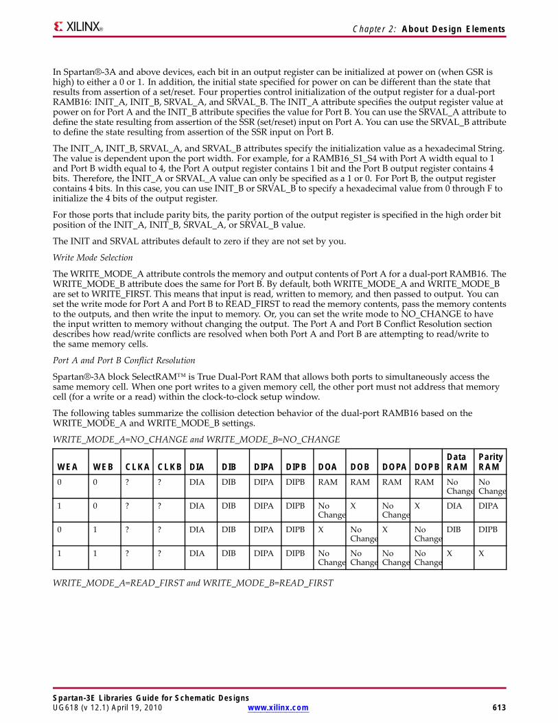
Chapter 2: About Design Elements
In Spartan®-3A and above devices, each bit in an output register can be initialized at power on (when GSR ishigh) to either a 0 or 1. In addition, the initial state specified for power on can be different than the state thatresults from assertion of a set/reset. Four properties control initialization of the output register for a dual-portRAMB16: INIT_A, INIT_B, SRVAL_A, and SRVAL_B. The INIT_A attribute specifies the output register value atpower on for Port A and the INIT_B attribute specifies the value for Port B. You can use the SRVAL_A attribute todefine the state resulting from assertion of the SSR (set/reset) input on Port A. You can use the SRVAL_B attributeto define the state resulting from assertion of the SSR input on Port B.
The INIT_A, INIT_B, SRVAL_A, and SRVAL_B attributes specify the initialization value as a hexadecimal String.The value is dependent upon the port width. For example, for a RAMB16_S1_S4 with Port A width equal to 1and Port B width equal to 4, the Port A output register contains 1 bit and the Port B output register contains 4bits. Therefore, the INIT_A or SRVAL_A value can only be specified as a 1 or 0. For Port B, the output registercontains 4 bits. In this case, you can use INIT_B or SRVAL_B to specify a hexadecimal value from 0 through F toinitialize the 4 bits of the output register.
For those ports that include parity bits, the parity portion of the output register is specified in the high order bitposition of the INIT_A, INIT_B, SRVAL_A, or SRVAL_B value.
The INIT and SRVAL attributes default to zero if they are not set by you.
Write Mode Selection
TheWRITE_MODE_A attribute controls the memory and output contents of Port A for a dual-port RAMB16. TheWRITE_MODE_B attribute does the same for Port B. By default, both WRITE_MODE_A and WRITE_MODE_Bare set to WRITE_FIRST. This means that input is read, written to memory, and then passed to output. You canset the write mode for Port A and Port B to READ_FIRST to read the memory contents, pass the memory contentsto the outputs, and then write the input to memory. Or, you can set the write mode to NO_CHANGE to havethe input written to memory without changing the output. The Port A and Port B Conflict Resolution sectiondescribes how read/write conflicts are resolved when both Port A and Port B are attempting to read/write tothe same memory cells.
Port A and Port B Conflict Resolution
Spartan®-3A block SelectRAM™ is True Dual-Port RAM that allows both ports to simultaneously access thesame memory cell. When one port writes to a given memory cell, the other port must not address that memorycell (for a write or a read) within the clock-to-clock setup window.
The following tables summarize the collision detection behavior of the dual-port RAMB16 based on theWRITE_MODE_A and WRITE_MODE_B settings.
WRITE_MODE_A=NO_CHANGE and WRITE_MODE_B=NO_CHANGE
WEA WEB CLKA CLKB DIA DIB DIPA DIPB DOA DOB DOPA DOPBDataRAM
ParityRAM
0 0 ? ? DIA DIB DIPA DIPB RAM RAM RAM RAM NoChange
NoChange
1 0 ? ? DIA DIB DIPA DIPB NoChange
X NoChange
X DIA DIPA
0 1 ? ? DIA DIB DIPA DIPB X NoChange
X NoChange
DIB DIPB
1 1 ? ? DIA DIB DIPA DIPB NoChange
NoChange
NoChange
NoChange
X X
WRITE_MODE_A=READ_FIRST and WRITE_MODE_B=READ_FIRST
Spartan-3E Libraries Guide for Schematic DesignsUG618 (v 12.1) April 19, 2010 www.xilinx.com 613

Chapter 2: About Design Elements
WEA WEB CLKA CLKB DIA DIB DIPA DIPB DOA DOB DOPA DOPBDataRAM
ParityRAM
0 0 ? ? DIA DIB DIPA DIPB RAM RAM RAM RAM NoChange
NoChange
1 0 ? ? DIA DIB DIPA DIPB RAM RAM RAM RAM DIA DIPA
0 1 ? ? DIA DIB DIPA DIPB RAM RAM RAM RAM DIB DIPB
1 1 ? ? DIA DIB DIPA DIPB RAM RAM RAM RAM X X
WRITE_MODE_A= WRITE_FIRST and WRITE_MODE_B=WRITE_FIRST
WEA WEB CLKA CLKB DIA DIB DIPA DIPB DOA DOB DOPA DOPBDataRAM
ParityRAM
0 0 ? ? DIA DIB DIPA DIPB RAM RAM RAM RAM NoChange
NoChange
1 0 ? ? DIA DIB DIPA DIPB DIA X DIPA X DIA DIPA
0 1 ? ? DIA DIB DIPA DIPB X DIB X DIPB DIB DIPB
1 1 ? ? DIA DIB DIPA DIPB X X X X X X
WRITE_MODE_A=NO_CHANGE and WRITE_MODE_B=READ_FIRST
WEA WEB CLKA CLKB DIA DIB DIPA DIPB DOA DOB DOPA DOPBDataRAM
ParityRAM
0 0 ? ? DIA DIB DIPA DIPB RAM RAM RAM RAM NoChange
NoChange
1 0 ? ? DIA DIB DIPA DIPB NoChange
X NoChange
X DIA DIPA
0 1 ? ? DIA DIB DIPA DIPB RAM RAM RAM RAM DIB DIPB
1 1 ? ? DIA DIB DIPA DIPB NoChange
X NoChange
X DIB DIPB
WRITE_MODE_A=NO_CHANGE and WRITE_MODE_B=WRITE_FIRST
WEA WEB CLKA CLKB DIA DIB DIPA DIPB DOA DOB DOPA DOPBDataRAM
ParityRAM
0 0 ? ? DIA DIB DIPA DIPB RAM RAM RAM RAM NoChange
NoChange
1 0 ? ? DIA DIB DIPA DIPB NoChange
X NoChange
X DIA DIPA
0 1 ? ? DIA DIB DIPA DIPB X DIB X DIPB DIB DIPB
1 1 ? ? DIA DIB DIPA DIPB NoChange
X NoChange
X X X
WRITE_MODE_A=READ_FIRST and WRITE_MODE_B=WRITE_FIRST
WEA WEB CLKA CLKB DIA DIB DIPA DIPB DOA DOB DOPA DOPBDataRAM
ParityRAM
0 0 ? ? DIA DIB DIPA DIPB RAM RAM RAM RAM NoChange
NoChange
1 0 ? ? DIA DIB DIPA DIPB RAM RAM RAM RAM DIA DIPA
0 1 ? ? DIA DIB DIPA DIPB X DIB X DIPB DIB DIPB
1 1 ? ? DIA DIB DIPA DIPB X DIB X DIPB DIA DIPA
Spartan-3E Libraries Guide for Schematic Designs614 www.xilinx.com UG618 (v 12.1) April 19, 2010
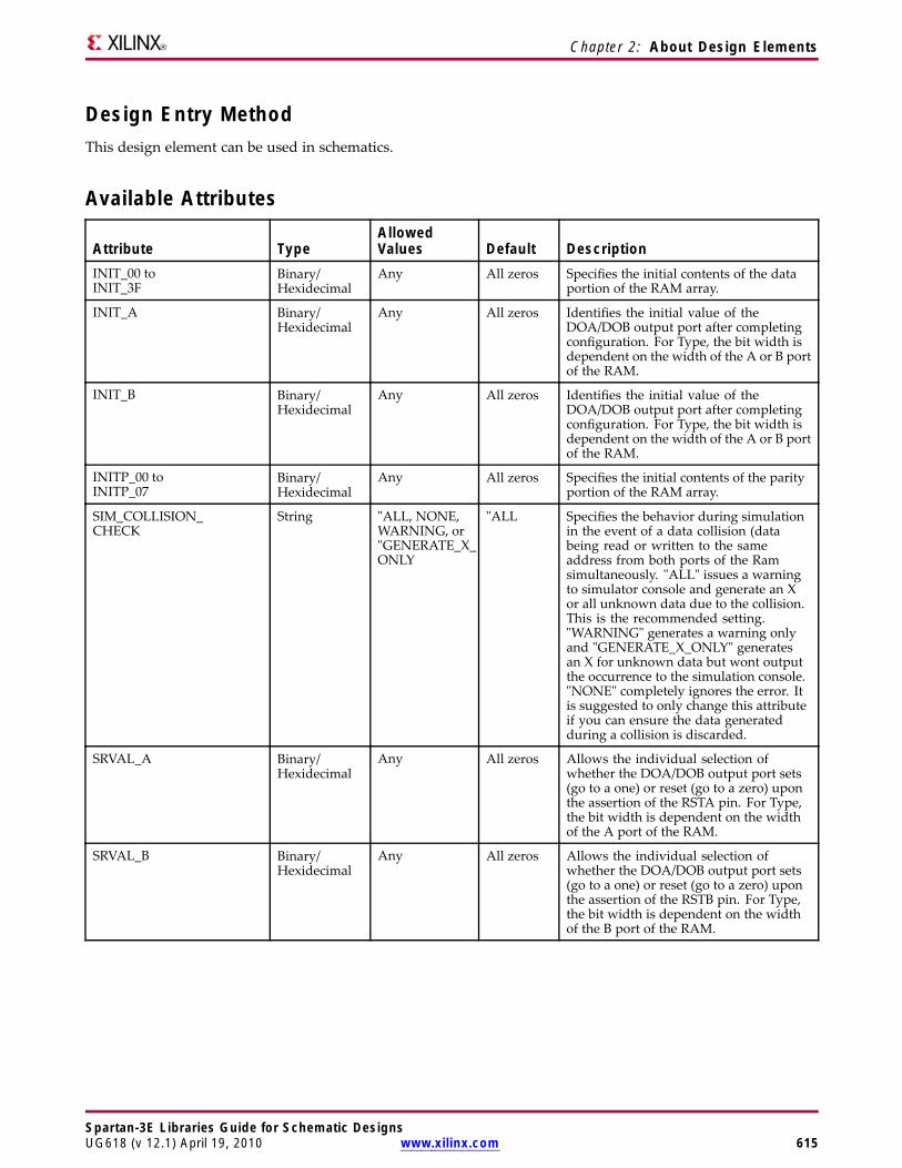
Chapter 2: About Design Elements
Design Entry MethodThis design element can be used in schematics.
Available Attributes
Attribute TypeAllowedValues Default Description
INIT_00 toINIT_3F
Binary/Hexidecimal
Any All zeros Specifies the initial contents of the dataportion of the RAM array.
INIT_A Binary/Hexidecimal
Any All zeros Identifies the initial value of theDOA/DOB output port after completingconfiguration. For Type, the bit width isdependent on the width of the A or B portof the RAM.
INIT_B Binary/Hexidecimal
Any All zeros Identifies the initial value of theDOA/DOB output port after completingconfiguration. For Type, the bit width isdependent on the width of the A or B portof the RAM.
INITP_00 toINITP_07
Binary/Hexidecimal
Any All zeros Specifies the initial contents of the parityportion of the RAM array.
SIM_COLLISION_CHECK
String "ALL, NONE,WARNING, or"GENERATE_X_ONLY
"ALL Specifies the behavior during simulationin the event of a data collision (databeing read or written to the sameaddress from both ports of the Ramsimultaneously. "ALL" issues a warningto simulator console and generate an Xor all unknown data due to the collision.This is the recommended setting."WARNING" generates a warning onlyand "GENERATE_X_ONLY" generatesan X for unknown data but wont outputthe occurrence to the simulation console."NONE" completely ignores the error. Itis suggested to only change this attributeif you can ensure the data generatedduring a collision is discarded.
SRVAL_A Binary/Hexidecimal
Any All zeros Allows the individual selection ofwhether the DOA/DOB output port sets(go to a one) or reset (go to a zero) uponthe assertion of the RSTA pin. For Type,the bit width is dependent on the widthof the A port of the RAM.
SRVAL_B Binary/Hexidecimal
Any All zeros Allows the individual selection ofwhether the DOA/DOB output port sets(go to a one) or reset (go to a zero) uponthe assertion of the RSTB pin. For Type,the bit width is dependent on the widthof the B port of the RAM.
Spartan-3E Libraries Guide for Schematic DesignsUG618 (v 12.1) April 19, 2010 www.xilinx.com 615
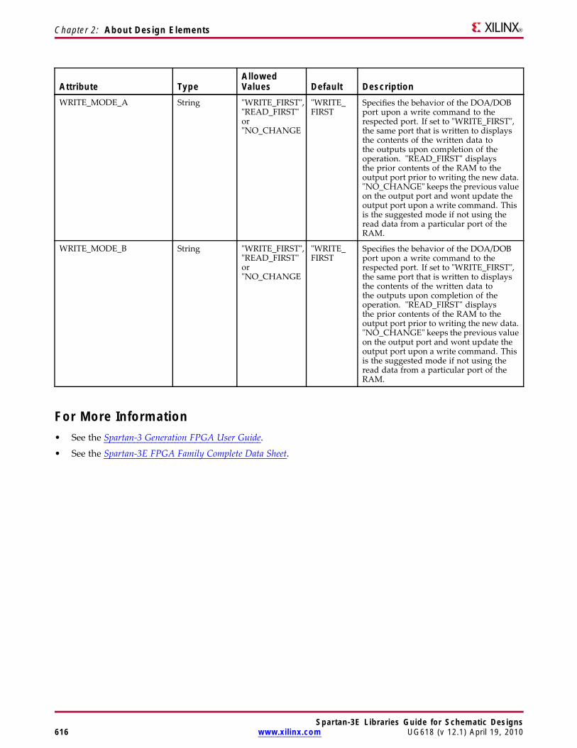
Chapter 2: About Design Elements
Attribute TypeAllowedValues Default Description
WRITE_MODE_A String "WRITE_FIRST","READ_FIRST"or"NO_CHANGE
"WRITE_FIRST
Specifies the behavior of the DOA/DOBport upon a write command to therespected port. If set to "WRITE_FIRST",the same port that is written to displaysthe contents of the written data tothe outputs upon completion of theoperation. "READ_FIRST" displaysthe prior contents of the RAM to theoutput port prior to writing the new data."NO_CHANGE" keeps the previous valueon the output port and wont update theoutput port upon a write command. Thisis the suggested mode if not using theread data from a particular port of theRAM.
WRITE_MODE_B String "WRITE_FIRST","READ_FIRST"or"NO_CHANGE
"WRITE_FIRST
Specifies the behavior of the DOA/DOBport upon a write command to therespected port. If set to "WRITE_FIRST",the same port that is written to displaysthe contents of the written data tothe outputs upon completion of theoperation. "READ_FIRST" displaysthe prior contents of the RAM to theoutput port prior to writing the new data."NO_CHANGE" keeps the previous valueon the output port and wont update theoutput port upon a write command. Thisis the suggested mode if not using theread data from a particular port of theRAM.
For More Information• See the Spartan-3 Generation FPGA User Guide.
• See the Spartan-3E FPGA Family Complete Data Sheet.
Spartan-3E Libraries Guide for Schematic Designs616 www.xilinx.com UG618 (v 12.1) April 19, 2010
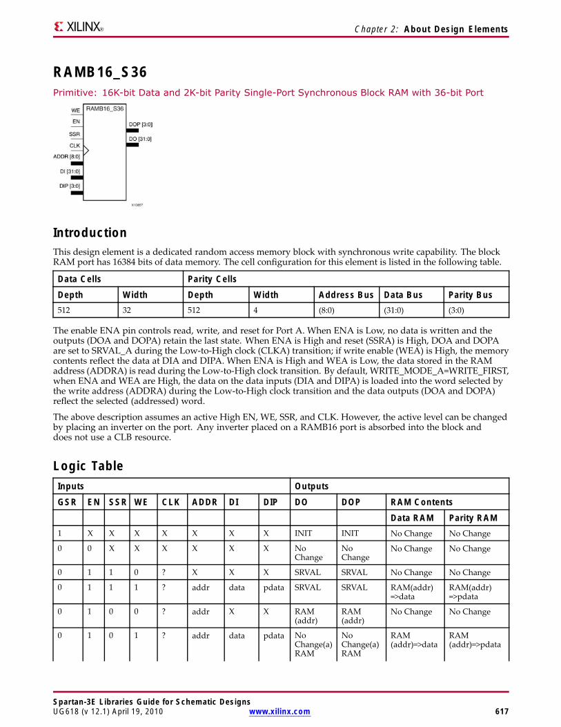
Chapter 2: About Design Elements
RAMB16_S36Primitive: 16K-bit Data and 2K-bit Parity Single-Port Synchronous Block RAM with 36-bit Port
IntroductionThis design element is a dedicated random access memory block with synchronous write capability. The blockRAM port has 16384 bits of data memory. The cell configuration for this element is listed in the following table.
Data Cells Parity CellsDepth Width Depth Width Address Bus Data Bus Parity Bus512 32 512 4 (8:0) (31:0) (3:0)
The enable ENA pin controls read, write, and reset for Port A. When ENA is Low, no data is written and theoutputs (DOA and DOPA) retain the last state. When ENA is High and reset (SSRA) is High, DOA and DOPAare set to SRVAL_A during the Low-to-High clock (CLKA) transition; if write enable (WEA) is High, the memorycontents reflect the data at DIA and DIPA. When ENA is High and WEA is Low, the data stored in the RAMaddress (ADDRA) is read during the Low-to-High clock transition. By default, WRITE_MODE_A=WRITE_FIRST,when ENA and WEA are High, the data on the data inputs (DIA and DIPA) is loaded into the word selected bythe write address (ADDRA) during the Low-to-High clock transition and the data outputs (DOA and DOPA)reflect the selected (addressed) word.
The above description assumes an active High EN, WE, SSR, and CLK. However, the active level can be changedby placing an inverter on the port. Any inverter placed on a RAMB16 port is absorbed into the block anddoes not use a CLB resource.
Logic TableInputs Outputs
GSR EN SSR WE CLK ADDR DI DIP DO DOP RAM ContentsData RAM Parity RAM
1 X X X X X X X INIT INIT No Change No Change
0 0 X X X X X X NoChange
NoChange
No Change No Change
0 1 1 0 ? X X X SRVAL SRVAL No Change No Change
0 1 1 1 ? addr data pdata SRVAL SRVAL RAM(addr)=>data
RAM(addr)=>pdata
0 1 0 0 ? addr X X RAM(addr)
RAM(addr)
No Change No Change
0 1 0 1 ? addr data pdata NoChange(a)RAM
NoChange(a)RAM
RAM(addr)=>data
RAM(addr)=>pdata
Spartan-3E Libraries Guide for Schematic DesignsUG618 (v 12.1) April 19, 2010 www.xilinx.com 617

Chapter 2: About Design Elements
Inputs Outputs
GSR EN SSR WE CLK ADDR DI DIP DO DOP RAM ContentsData RAM Parity RAM
(addr)(b)data(c)
(addr)(b)pdata(c)
GSR=Global Set Reset signal
INIT=Value specified by the INIT attribute for data memory. Default is all zeros.
SRVAL=Value after assertion of SSR as specified by the SRVAL attribute.
addr=RAM address.
RAM(addr)=RAM contents at address ADDR.
data=RAM input data.
pdata=RAM parity data.
(a) WRITE_MODE=NO_CHANGE
(b) WRITE_MODE=READ_FIRST
(c) WRITE_MODE=WRITE_FIRST
InitializationInitializing Memory Contents
You can use the INIT_xx attributes to specify an initialization value for the memory contents of a RAMB16 duringdevice configuration. The initialization of each RAMB16 is set by 64 initialization attributes (INIT_00 throughINIT_3F) of 64 hex values for a total of 16384 bits.
You can use the INITP_xx attributes to specify an initial value for the parity memory during device configurationor assertion. The initialization of the parity memory for ports configured for 9, 18, or 36 bits is set by 8initialization attributes (INITP_00 through INITP_07) of 64 hex values for a total of 2048 bits.
Any INIT_xx or INITP_xx attribute that is not specified is configured as zeros. Partial Strings are paddedwith zeros to the left.
Initializing the Output Register
In Spartan®-3A and above devices, each bit in the output register can be initialized at power on to either a 0 or 1.In addition, the initial state specified for power on can be different than the state that results from assertion of aset/reset. Two types of properties control initialization of the output register for a single-port RAMB16: INIT andSRVAL. The INIT attribute specifies the output register value at power on. You can use the SRVAL attributeto define the state resulting from assertion of the SSR (set/reset) input.
The INIT and SRVAL attributes specify the initialization value as a hexadecimal String containing one bit foreach bit in the output port. For example, for a RAMB16_S1 with port width equal to 1, the output registercontains 1 bit. Therefore, the INIT or SRVAL value can only be specified as a 1 or 0. For RAMB16_S4 with portwidth equal to 4, the output register contains 4 bits. In this case, you can specify a hexadecimal value from 0through F to initialize the 4 bits of the output register.
For those ports that include parity bits, the parity portion of the output register is specified in the high orderbit position of the INIT or SRVAL value.
Selecting Write Mode
The WRITE_MODE attribute controls RAMB16 memory and output contents. By default, the WRITE_MODE isset to WRITE_FIRST. This means that input is read, written to memory, and then passed to output. You can setthe WRITE_MODE to READ_FIRST to read the memory contents, pass the memory contents to the outputs, andthen write the input to memory. Or, you can set the WRITE_MODE to NO_CHANGE to have the input writtento memory without changing the output.
Spartan-3E Libraries Guide for Schematic Designs618 www.xilinx.com UG618 (v 12.1) April 19, 2010

Chapter 2: About Design Elements
Design Entry MethodThis design element can be used in schematics.
Available Attributes
Attribute TypeAllowedValues Default Description
INIT Binary/Hexadecimal
Any Hex Value All zeros Identifies the initial value of theDO output port after completingconfiguration. The bit width is dependenton the width of the A or B port of theRAM.
INIT_00 toINIT_3F
Binary/Hexadecimal
Any Hex Value All zeros Specifies the initial contents of the dataportion of the RAM array.
INITP_00 toINITP_07
Binary/Hexadecimal
Any Hex Value All zeros Specifies the initial contents of the parityportion of the RAM array.
SRVAL Binary/Hexadecimal
Any Hex Value All zeros Allows the individual selection ofwhether the DO output port sets (go toa one) or reset (go to a zero) upon theassertion of the SSR pin. The bit widthis dependent on the width of the A or Bport of the RAM.
WRITE_MODE String "WRITE_FIRST","READ_FIRST"or"NO_CHANGE"
"WRITE_FIRST" Specifies the behavior of the DO portupon a write command to the respectedport. If set to "WRITE_FIRST", thesame port that is written to displaysthe contents of the written data tothe outputs upon completion of theoperation. "READ_FIRST" displaysthe prior contents of the RAM to theoutput port prior to writing the newdata. "NO_CHANGE" keeps the previousvalue on the output port and wont updatethe output port upon a write command.This is the suggested mode if not usingthe read data from a particular port of theRAM.
For More Information• See the Spartan-3 Generation FPGA User Guide.
• See the Spartan-3E FPGA Family Complete Data Sheet.
Spartan-3E Libraries Guide for Schematic DesignsUG618 (v 12.1) April 19, 2010 www.xilinx.com 619

Spartan-3E Libraries Guide for Schematic Designs620 www.xilinx.com UG618 (v 12.1) April 19, 2010
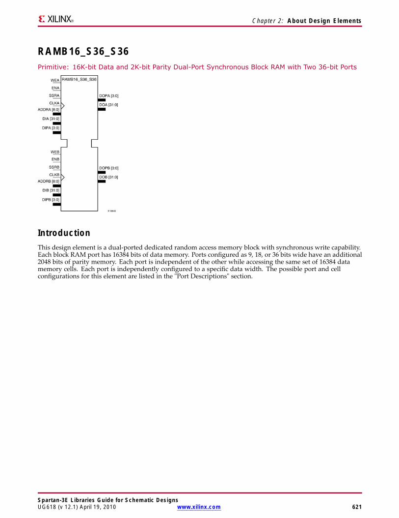
Chapter 2: About Design Elements
RAMB16_S36_S36Primitive: 16K-bit Data and 2K-bit Parity Dual-Port Synchronous Block RAM with Two 36-bit Ports
IntroductionThis design element is a dual-ported dedicated random access memory block with synchronous write capability.Each block RAM port has 16384 bits of data memory. Ports configured as 9, 18, or 36 bits wide have an additional2048 bits of parity memory. Each port is independent of the other while accessing the same set of 16384 datamemory cells. Each port is independently configured to a specific data width. The possible port and cellconfigurations for this element are listed in the "Port Descriptions" section.
Spartan-3E Libraries Guide for Schematic DesignsUG618 (v 12.1) April 19, 2010 www.xilinx.com 621

Chapter 2: About Design Elements
Logic TableTruth Table A
Inputs Outputs
GSR ENA SSRA WEA CLKA ADDRA DIA DIPA DOA DOPA RAM ContentsData RAM Parity RAM
1 X X X X X X X INIT_A INIT_A No Change No Change
0 0 X X X X X X No Change No Change No Change No Change
0 1 1 0 ? X X X SRVAL_A SRVAL_A No Change No Change
0 1 1 1 ? addr data pdata SRVAL_A SRVAL_A RAM(addr)=>data
RAM(addr)=>pdata
0 1 0 0 ? addr X X RAM(addr) RAM(addr) No Change No Change
0 1 0 1 ? addr data pdata No Change1,RAM(addr)2,data3
No Change1,RAM(addr)2,pdata3
RAM(addr)=>data
RAM(addr)=>pdata
GSR=Global Set Reset.
INIT_A=Value specified by the INIT_A attribute for output register. Default is all zeros.
SRVAL_A=register value.
addr=RAM address.
RAM(addr)=RAM contents at address ADDR.
data=RAM input data.
pdata=RAM parity data.
1WRITE_MODE_A=NO_CHANGE.
2WRITE_MODE_A=READ_FIRST.
3WRITE_MODE_A=WRITE_FIRST.
Spartan-3E Libraries Guide for Schematic Designs622 www.xilinx.com UG618 (v 12.1) April 19, 2010
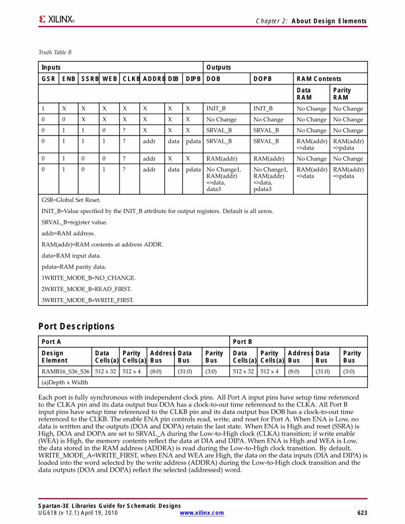
Chapter 2: About Design Elements
Truth Table B
Inputs Outputs
GSR ENB SSRB WEB CLKB ADDRB DIB DIPB DOB DOPB RAM ContentsDataRAM
ParityRAM
1 X X X X X X X INIT_B INIT_B No Change No Change
0 0 X X X X X X No Change No Change No Change No Change
0 1 1 0 ? X X X SRVAL_B SRVAL_B No Change No Change
0 1 1 1 ? addr data pdata SRVAL_B SRVAL_B RAM(addr)=>data
RAM(addr)=>pdata
0 1 0 0 ? addr X X RAM(addr) RAM(addr) No Change No Change
0 1 0 1 ? addr data pdata No Change1,RAM(addr)=>data,data3
No Change1,RAM(addr)=>data,pdata3
RAM(addr)=>data
RAM(addr)=>pdata
GSR=Global Set Reset.
INIT_B=Value specified by the INIT_B attribute for output registers. Default is all zeros.
SRVAL_B=register value.
addr=RAM address.
RAM(addr)=RAM contents at address ADDR.
data=RAM input data.
pdata=RAM parity data.
1WRITE_MODE_B=NO_CHANGE.
2WRITE_MODE_B=READ_FIRST.
3WRITE_MODE_B=WRITE_FIRST.
Port DescriptionsPort A Port BDesignElement
DataCells(a)
ParityCells(a)
AddressBus
DataBus
ParityBus
DataCells(a)
ParityCells(a)
AddressBus
DataBus
ParityBus
RAMB16_S36_S36 512 x 32 512 x 4 (8:0) (31:0) (3:0) 512 x 32 512 x 4 (8:0) (31:0) (3:0)
(a)Depth x Width
Each port is fully synchronous with independent clock pins. All Port A input pins have setup time referencedto the CLKA pin and its data output bus DOA has a clock-to-out time referenced to the CLKA. All Port Binput pins have setup time referenced to the CLKB pin and its data output bus DOB has a clock-to-out timereferenced to the CLKB. The enable ENA pin controls read, write, and reset for Port A. When ENA is Low, nodata is written and the outputs (DOA and DOPA) retain the last state. When ENA is High and reset (SSRA) isHigh, DOA and DOPA are set to SRVAL_A during the Low-to-High clock (CLKA) transition; if write enable(WEA) is High, the memory contents reflect the data at DIA and DIPA. When ENA is High and WEA is Low,the data stored in the RAM address (ADDRA) is read during the Low-to-High clock transition. By default,WRITE_MODE_A=WRITE_FIRST, when ENA and WEA are High, the data on the data inputs (DIA and DIPA) isloaded into the word selected by the write address (ADDRA) during the Low-to-High clock transition and thedata outputs (DOA and DOPA) reflect the selected (addressed) word.
Spartan-3E Libraries Guide for Schematic DesignsUG618 (v 12.1) April 19, 2010 www.xilinx.com 623

Chapter 2: About Design Elements
The enable ENB pin controls read, write, and reset for Port B. When ENB is Low, no data is written and theoutputs (DOB and DOPB) retain the last state. When ENB is High and reset (SSRB) is High, DOB and DOPB areset to SRVAL_B during the Low-to-High clock (CLKB) transition; if write enable (WEB) is High, the memorycontents reflect the data at DIB and DIPB. When ENB is High and WEB is Low, the data stored in the RAMaddress (ADDRB) is read during the Low-to-High clock transition. By default, WRITE_MODE_B=WRITE_FIRST,when ENB and WEB are High, the data on the data inputs (DIB and PB) are loaded into the word selected by thewrite address (ADDRB) during the Low-to-High clock transition and the data outputs (DOB and DOPB) reflectthe selected (addressed) word. The above descriptions assume active High control pins (ENA, WEA, SSRA,CLKA, ENB, WEB, SSRB, and CLKB). However, the active level can be changed by placing an inverter on theport. Any inverter placed on a RAMB16 port is absorbed into the block and does not use a CLB resource.
Address Mapping
Each port accesses the same set of 18432 memory cells using an addressing scheme that is dependent on thewidth of the port. For all port widths, 16384 memory cells are available for data as shown in the Port AddressMapping for Data table below. For 9-, 18-, and 36-bit wide ports, 2408 parity memory cells are also availableas shown in Port Address Mapping for Parity table below. The physical RAM location that is addressed for aparticular width is determined from the following formula.
Start=((ADDR port+1)*(Widthport)) -1
End=(ADDRport)*(Widthport)
The following tables show address mapping for each port width.
Port Address Mapping for Data
DataWidth Port Data Addresses1 16384 <-- 31 30 29 28 27 26 25 24 23 22 21 20 19 18 17 16 15 14 13 12 11 10 9 8 7 6 5 4 3 2 1 0
2 8192 <-- 15 14 13 12 11 10 9 8 7 6 5 4 3 2 1 0
4 4096 <-- 7 6 5 4 3 2 1 0
8 2048 <-- 3 2 1 0
16 1024 <-- 1 0
32 512 <-- 0
Port Address Mapping for Parity
ParityWidth Port Parity Addresses1 2048 <--- 3 2 1 0
2 1024 <--- 1 0
4 512 <--- 0
Initializing Memory Contents of a Dual-Port RAMB16
You can use the INIT_xx attributes to specify an initialization value for the memory contents of a RAMB16 duringdevice configuration. The initialization of each RAMB16_Sm_Sn is set by 64 initialization attributes (INIT_00through INIT_3F) of 64 hex values for a total of 16384 bits.
You can use the INITP_xx attributes to specify an initial value for the parity memory during device configurationor assertion. The initialization of the parity memory for ports configured for 9, 18, or 36 bits is set by 8initialization attributes (INITP_00 through INITP_07) of 64 hex values for a total of 2048 bits.
If any INIT_xx or INITP_xx attribute is not specified, it is configured as zeros. Partial Strings are padded withzeros to the left.
Spartan-3E Libraries Guide for Schematic Designs624 www.xilinx.com UG618 (v 12.1) April 19, 2010

Chapter 2: About Design Elements
Initializing the Output Register of a Dual-Port RAMB16
In Spartan®-3A and above devices, each bit in an output register can be initialized at power on (when GSR ishigh) to either a 0 or 1. In addition, the initial state specified for power on can be different than the state thatresults from assertion of a set/reset. Four properties control initialization of the output register for a dual-portRAMB16: INIT_A, INIT_B, SRVAL_A, and SRVAL_B. The INIT_A attribute specifies the output register value atpower on for Port A and the INIT_B attribute specifies the value for Port B. You can use the SRVAL_A attribute todefine the state resulting from assertion of the SSR (set/reset) input on Port A. You can use the SRVAL_B attributeto define the state resulting from assertion of the SSR input on Port B.
The INIT_A, INIT_B, SRVAL_A, and SRVAL_B attributes specify the initialization value as a hexadecimal String.The value is dependent upon the port width. For example, for a RAMB16_S1_S4 with Port A width equal to 1and Port B width equal to 4, the Port A output register contains 1 bit and the Port B output register contains 4bits. Therefore, the INIT_A or SRVAL_A value can only be specified as a 1 or 0. For Port B, the output registercontains 4 bits. In this case, you can use INIT_B or SRVAL_B to specify a hexadecimal value from 0 through F toinitialize the 4 bits of the output register.
For those ports that include parity bits, the parity portion of the output register is specified in the high order bitposition of the INIT_A, INIT_B, SRVAL_A, or SRVAL_B value.
The INIT and SRVAL attributes default to zero if they are not set by you.
Write Mode Selection
TheWRITE_MODE_A attribute controls the memory and output contents of Port A for a dual-port RAMB16. TheWRITE_MODE_B attribute does the same for Port B. By default, both WRITE_MODE_A and WRITE_MODE_Bare set to WRITE_FIRST. This means that input is read, written to memory, and then passed to output. You canset the write mode for Port A and Port B to READ_FIRST to read the memory contents, pass the memory contentsto the outputs, and then write the input to memory. Or, you can set the write mode to NO_CHANGE to havethe input written to memory without changing the output. The Port A and Port B Conflict Resolution sectiondescribes how read/write conflicts are resolved when both Port A and Port B are attempting to read/write tothe same memory cells.
Port A and Port B Conflict Resolution
Spartan-3A block SelectRAM™ is True Dual-Port RAM that allows both ports to simultaneously access the samememory cell. When one port writes to a given memory cell, the other port must not address that memory cell (fora write or a read) within the clock-to-clock setup window.
The following tables summarize the collision detection behavior of the dual-port RAMB16 based on theWRITE_MODE_A and WRITE_MODE_B settings.
WRITE_MODE_A=NO_CHANGE and WRITE_MODE_B=NO_CHANGE
WEA WEB CLKA CLKB DIA DIB DIPA DIPB DOA DOB DOPA DOPBDataRAM
ParityRAM
0 0 ? ? DIA DIB DIPA DIPB RAM RAM RAM RAM NoChange
NoChange
1 0 ? ? DIA DIB DIPA DIPB NoChange
X NoChange
X DIA DIPA
0 1 ? ? DIA DIB DIPA DIPB X NoChange
X NoChange
DIB DIPB
1 1 ? ? DIA DIB DIPA DIPB NoChange
NoChange
NoChange
NoChange
X X
Spartan-3E Libraries Guide for Schematic DesignsUG618 (v 12.1) April 19, 2010 www.xilinx.com 625

Chapter 2: About Design Elements
WRITE_MODE_A=READ_FIRST and WRITE_MODE_B=READ_FIRST
WEA WEB CLKA CLKB DIA DIB DIPA DIPB DOA DOB DOPA DOPBDataRAM
ParityRAM
0 0 ? ? DIA DIB DIPA DIPB RAM RAM RAM RAM NoChange
NoChange
1 0 ? ? DIA DIB DIPA DIPB RAM RAM RAM RAM DIA DIPA
0 1 ? ? DIA DIB DIPA DIPB RAM RAM RAM RAM DIB DIPB
1 1 ? ? DIA DIB DIPA DIPB RAM RAM RAM RAM X X
WRITE_MODE_A= WRITE_FIRST and WRITE_MODE_B=WRITE_FIRST
WEA WEB CLKA CLKB DIA DIB DIPA DIPB DOA DOB DOPA DOPBDataRAM
ParityRAM
0 0 ? ? DIA DIB DIPA DIPB RAM RAM RAM RAM NoChange
NoChange
1 0 ? ? DIA DIB DIPA DIPB DIA X DIPA X DIA DIPA
0 1 ? ? DIA DIB DIPA DIPB X DIB X DIPB DIB DIPB
1 1 ? ? DIA DIB DIPA DIPB X X X X X X
WRITE_MODE_A=NO_CHANGE and WRITE_MODE_B=READ_FIRST
WEA WEB CLKA CLKB DIA DIB DIPA DIPB DOA DOB DOPA DOPBDataRAM
ParityRAM
0 0 ? ? DIA DIB DIPA DIPB RAM RAM RAM RAM NoChange
NoChange
1 0 ? ? DIA DIB DIPA DIPB NoChange
X NoChange
X DIA DIPA
0 1 ? ? DIA DIB DIPA DIPB RAM RAM RAM RAM DIB DIPB
1 1 ? ? DIA DIB DIPA DIPB NoChange
X NoChange
X DIB DIPB
WRITE_MODE_A=NO_CHANGE and WRITE_MODE_B=WRITE_FIRST
WEA WEB CLKA CLKB DIA DIB DIPA DIPB DOA DOB DOPA DOPBDataRAM
ParityRAM
0 0 ? ? DIA DIB DIPA DIPB RAM RAM RAM RAM NoChange
NoChange
1 0 ? ? DIA DIB DIPA DIPB NoChange
X NoChange
X DIA DIPA
0 1 ? ? DIA DIB DIPA DIPB X DIB X DIPB DIB DIPB
1 1 ? ? DIA DIB DIPA DIPB NoChange
X NoChange
X X X
Spartan-3E Libraries Guide for Schematic Designs626 www.xilinx.com UG618 (v 12.1) April 19, 2010

Chapter 2: About Design Elements
WRITE_MODE_A=READ_FIRST and WRITE_MODE_B=WRITE_FIRST
WEA WEB CLKA CLKB DIA DIB DIPA DIPB DOA DOB DOPA DOPBDataRAM
ParityRAM
0 0 ? ? DIA DIB DIPA DIPB RAM RAM RAM RAM NoChange
NoChange
1 0 ? ? DIA DIB DIPA DIPB RAM RAM RAM RAM DIA DIPA
0 1 ? ? DIA DIB DIPA DIPB X DIB X DIPB DIB DIPB
1 1 ? ? DIA DIB DIPA DIPB X DIB X DIPB DIA DIPA
Design Entry MethodThis design element can be used in schematics.
Available Attributes
Attribute TypeAllowedValues Default Description
INIT_00 toINIT_3F
Binary/Hexadecimal
Any All zeros Specifies the initial contents of the data portionof the RAM array.
INIT_A Binary/Hexadecimal
Any All zeros Identifies the initial value of the DOA/DOB outputport after completing configuration. For Type, thebit width is dependent on the width of the A or Bport of the RAM.
INIT_B Binary/Hexadecimal
Any All zeros Identifies the initial value of the DOA/DOB outputport after completing configuration. For Type, thebit width is dependent on the width of the A or Bport of the RAM.
INITP_00 toINITP_07
Binary/Hexadecimal
Any All zeros Specifies the initial contents of the parity portionof the RAM array.
SIM_COLLISION_CHECK
String "ALL,WARNING_ONLY,"GENERATE_X_ONLY,NONE
"ALL Allows modification of the simulation behavior ifa memory collision occurs. The output is affectedas follows:
• "ALL" - Warning produced and affectedoutputs/memory location go unknown (X).
• "WARNING_ONLY" - Warning produced andaffected outputs/memory retain last value.
• "GENERATE_X_ONLY" - No warning.However, affected outputs/memory gounknown (X).
• "NONE" - No warning and affectedoutputs/memory retain last value.
Note Setting this to a value other than "ALL" canallow problems in the design go unnoticed duringsimulation. Care should be taken when changingthe value of this attribute. Please see the Synthesisand Simulation Design Guide for more information.
SRVAL_A Binary/Hexadecimal
Any All zeros Allows the individual selection of whether theDOA/DOB output port sets (go to a one) or reset(go to a zero) upon the assertion of the RSTA pin.For Type, the bit width is dependent on the widthof the A port of the RAM.
Spartan-3E Libraries Guide for Schematic DesignsUG618 (v 12.1) April 19, 2010 www.xilinx.com 627

Chapter 2: About Design Elements
Attribute TypeAllowedValues Default Description
SRVAL_B Binary/Hexadecimal
Any All zeros Allows the individual selection of whether theDOA/DOB output port sets (go to a one) or reset(go to a zero) upon the assertion of the RSTB pin.For Type, the bit width is dependent on the widthof the B port of the RAM.
WRITE_MODE_A String "WRITE_FIRST","READ_FIRST","NO_CHANGE
"WRITE_FIRST
Specifies the behavior of the DOA/DOB port upona write command to the respected port. If set to"WRITE_FIRST", the same port that is writtento displays the contents of the written data tothe outputs upon completion of the operation."READ_FIRST" displays the prior contents of theRAM to the output port prior to writing the newdata. "NO_CHANGE" keeps the previous valueon the output port and wont update the outputport upon a write command. This is the suggestedmode if not using the read data from a particularport of the RAM.
WRITE_MODE_B String "WRITE_FIRST","READ_FIRST","NO_CHANGE
"WRITE_FIRST
Specifies the behavior of the DOA/DOB port upona write command to the respected port. If set to"WRITE_FIRST", the same port that is writtento displays the contents of the written data tothe outputs upon completion of the operation."READ_FIRST" displays the prior contents of theRAM to the output port prior to writing the newdata. "NO_CHANGE" keeps the previous valueon the output port and wont update the outputport upon a write command. This is the suggestedmode if not using the read data from a particularport of the RAM.
For More Information• See the Spartan-3 Generation FPGA User Guide.
• See the Spartan-3E FPGA Family Complete Data Sheet.
Spartan-3E Libraries Guide for Schematic Designs628 www.xilinx.com UG618 (v 12.1) April 19, 2010
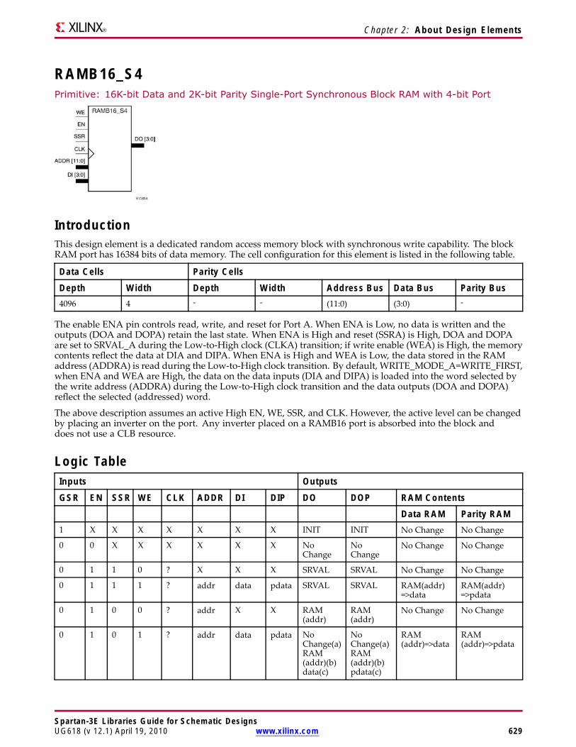
Chapter 2: About Design Elements
RAMB16_S4Primitive: 16K-bit Data and 2K-bit Parity Single-Port Synchronous Block RAM with 4-bit Port
IntroductionThis design element is a dedicated random access memory block with synchronous write capability. The blockRAM port has 16384 bits of data memory. The cell configuration for this element is listed in the following table.
Data Cells Parity CellsDepth Width Depth Width Address Bus Data Bus Parity Bus4096 4 - - (11:0) (3:0) -
The enable ENA pin controls read, write, and reset for Port A. When ENA is Low, no data is written and theoutputs (DOA and DOPA) retain the last state. When ENA is High and reset (SSRA) is High, DOA and DOPAare set to SRVAL_A during the Low-to-High clock (CLKA) transition; if write enable (WEA) is High, the memorycontents reflect the data at DIA and DIPA. When ENA is High and WEA is Low, the data stored in the RAMaddress (ADDRA) is read during the Low-to-High clock transition. By default, WRITE_MODE_A=WRITE_FIRST,when ENA and WEA are High, the data on the data inputs (DIA and DIPA) is loaded into the word selected bythe write address (ADDRA) during the Low-to-High clock transition and the data outputs (DOA and DOPA)reflect the selected (addressed) word.
The above description assumes an active High EN, WE, SSR, and CLK. However, the active level can be changedby placing an inverter on the port. Any inverter placed on a RAMB16 port is absorbed into the block anddoes not use a CLB resource.
Logic TableInputs Outputs
GSR EN SSR WE CLK ADDR DI DIP DO DOP RAM ContentsData RAM Parity RAM
1 X X X X X X X INIT INIT No Change No Change
0 0 X X X X X X NoChange
NoChange
No Change No Change
0 1 1 0 ? X X X SRVAL SRVAL No Change No Change
0 1 1 1 ? addr data pdata SRVAL SRVAL RAM(addr)=>data
RAM(addr)=>pdata
0 1 0 0 ? addr X X RAM(addr)
RAM(addr)
No Change No Change
0 1 0 1 ? addr data pdata NoChange(a)RAM(addr)(b)data(c)
NoChange(a)RAM(addr)(b)pdata(c)
RAM(addr)=>data
RAM(addr)=>pdata
Spartan-3E Libraries Guide for Schematic DesignsUG618 (v 12.1) April 19, 2010 www.xilinx.com 629

Chapter 2: About Design Elements
Inputs Outputs
GSR EN SSR WE CLK ADDR DI DIP DO DOP RAM ContentsData RAM Parity RAM
GSR=Global Set Reset signal
INIT=Value specified by the INIT attribute for data memory. Default is all zeros.
SRVAL=Value after assertion of SSR as specified by the SRVAL attribute.
addr=RAM address.
RAM(addr)=RAM contents at address ADDR.
data=RAM input data.
pdata=RAM parity data.
(a) WRITE_MODE=NO_CHANGE
(b) WRITE_MODE=READ_FIRST
(c) WRITE_MODE=WRITE_FIRST
InitializationInitializing Memory Contents
You can use the INIT_xx attributes to specify an initialization value for the memory contents of a RAMB16 duringdevice configuration. The initialization of each RAMB16 is set by 64 initialization attributes (INIT_00 throughINIT_3F) of 64 hex values for a total of 16384 bits.
You can use the INITP_xx attributes to specify an initial value for the parity memory during device configurationor assertion. The initialization of the parity memory for ports configured for 9, 18, or 36 bits is set by 8initialization attributes (INITP_00 through INITP_07) of 64 hex values for a total of 2048 bits.
Any INIT_xx or INITP_xx attribute that is not specified is configured as zeros. Partial Strings are paddedwith zeros to the left.
Initializing the Output Register
In Spartan®-3A and above devices, each bit in the output register can be initialized at power on to either a 0 or 1.In addition, the initial state specified for power on can be different than the state that results from assertion of aset/reset. Two types of properties control initialization of the output register for a single-port RAMB16: INIT andSRVAL. The INIT attribute specifies the output register value at power on. You can use the SRVAL attributeto define the state resulting from assertion of the SSR (set/reset) input.
The INIT and SRVAL attributes specify the initialization value as a hexadecimal String containing one bit foreach bit in the output port. For example, for a RAMB16_S1 with port width equal to 1, the output registercontains 1 bit. Therefore, the INIT or SRVAL value can only be specified as a 1 or 0. For RAMB16_S4 with portwidth equal to 4, the output register contains 4 bits. In this case, you can specify a hexadecimal value from 0through F to initialize the 4 bits of the output register.
For those ports that include parity bits, the parity portion of the output register is specified in the high orderbit position of the INIT or SRVAL value.
Selecting Write Mode
The WRITE_MODE attribute controls RAMB16 memory and output contents. By default, the WRITE_MODE isset to WRITE_FIRST. This means that input is read, written to memory, and then passed to output. You can setthe WRITE_MODE to READ_FIRST to read the memory contents, pass the memory contents to the outputs, andthen write the input to memory. Or, you can set the WRITE_MODE to NO_CHANGE to have the input writtento memory without changing the output.
Spartan-3E Libraries Guide for Schematic Designs630 www.xilinx.com UG618 (v 12.1) April 19, 2010

Chapter 2: About Design Elements
Design Entry MethodThis design element can be used in schematics.
Available Attributes
Attribute TypeAllowedValues Default Description
INIT Binary/Hexadecimal
Any Hex Value All zeros Identifies the initial value of theDO output port after completingconfiguration. The bit width is dependenton the width of the A or B port of theRAM.
INIT_00 toINIT_3F
Binary/Hexadecimal
Any Hex Value All zeros Specifies the initial contents of the dataportion of the RAM array.
INITP_00 toINITP_07
Binary/Hexadecimal
Any Hex Value All zeros Specifies the initial contents of the parityportion of the RAM array.
SRVAL Binary/Hexadecimal
Any Hex Value All zeros Allows the individual selection ofwhether the DO output port sets (go toa one) or reset (go to a zero) upon theassertion of the SSR pin. The bit widthis dependent on the width of the A or Bport of the RAM.
WRITE_MODE String "WRITE_FIRST","READ_FIRST"or"NO_CHANGE"
"WRITE_FIRST" Specifies the behavior of the DO portupon a write command to the respectedport. If set to "WRITE_FIRST", thesame port that is written to displaysthe contents of the written data tothe outputs upon completion of theoperation. "READ_FIRST" displaysthe prior contents of the RAM to theoutput port prior to writing the newdata. "NO_CHANGE" keeps the previousvalue on the output port and wont updatethe output port upon a write command.This is the suggested mode if not usingthe read data from a particular port of theRAM.
For More Information• See the Spartan-3 Generation FPGA User Guide.
• See the Spartan-3E FPGA Family Complete Data Sheet.
Spartan-3E Libraries Guide for Schematic DesignsUG618 (v 12.1) April 19, 2010 www.xilinx.com 631

Spartan-3E Libraries Guide for Schematic Designs632 www.xilinx.com UG618 (v 12.1) April 19, 2010
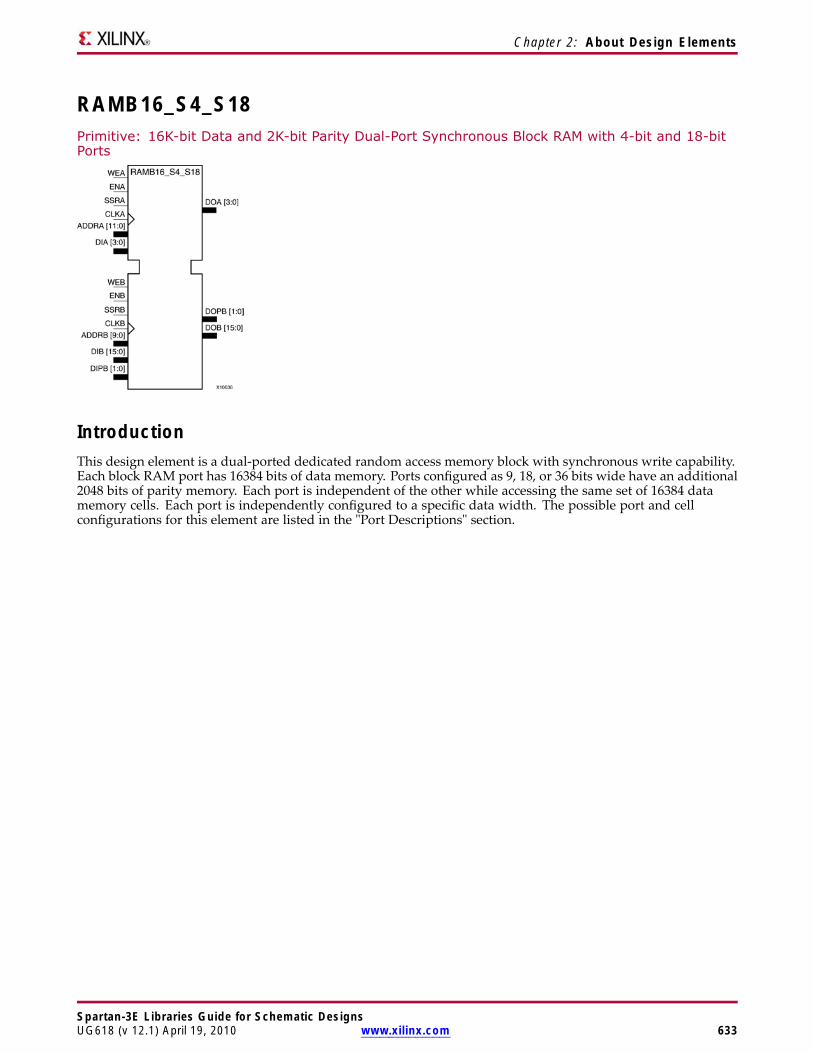
Chapter 2: About Design Elements
RAMB16_S4_S18Primitive: 16K-bit Data and 2K-bit Parity Dual-Port Synchronous Block RAM with 4-bit and 18-bitPorts
IntroductionThis design element is a dual-ported dedicated random access memory block with synchronous write capability.Each block RAM port has 16384 bits of data memory. Ports configured as 9, 18, or 36 bits wide have an additional2048 bits of parity memory. Each port is independent of the other while accessing the same set of 16384 datamemory cells. Each port is independently configured to a specific data width. The possible port and cellconfigurations for this element are listed in the "Port Descriptions" section.
Spartan-3E Libraries Guide for Schematic DesignsUG618 (v 12.1) April 19, 2010 www.xilinx.com 633

Chapter 2: About Design Elements
Logic TableTruth Table A
Inputs Outputs
GSR ENA SSRA WEA CLKA ADDRA DIA DIPA DOA DOPA RAM ContentsData RAM Parity RAM
1 X X X X X X X INIT_A INIT_A No Change No Change
0 0 X X X X X X No Change No Change No Change No Change
0 1 1 0 ? X X X SRVAL_A SRVAL_A No Change No Change
0 1 1 1 ? addr data pdata SRVAL_A SRVAL_A RAM(addr)=>data
RAM(addr)=>pdata
0 1 0 0 ? addr X X RAM(addr) RAM(addr) No Change No Change
0 1 0 1 ? addr data pdata No Change1,RAM(addr)2,data3
No Change1,RAM(addr)2,pdata3
RAM(addr)=>data
RAM(addr)=>pdata
GSR=Global Set Reset.
INIT_A=Value specified by the INIT_A attribute for output register. Default is all zeros.
SRVAL_A=register value.
addr=RAM address.
RAM(addr)=RAM contents at address ADDR.
data=RAM input data.
pdata=RAM parity data.
1WRITE_MODE_A=NO_CHANGE.
2WRITE_MODE_A=READ_FIRST.
3WRITE_MODE_A=WRITE_FIRST.
Spartan-3E Libraries Guide for Schematic Designs634 www.xilinx.com UG618 (v 12.1) April 19, 2010

Chapter 2: About Design Elements
Truth Table B
Inputs Outputs
GSR ENB SSRB WEB CLKB ADDRB DIB DIPB DOB DOPB RAM ContentsDataRAM
ParityRAM
1 X X X X X X X INIT_B INIT_B No Change No Change
0 0 X X X X X X No Change No Change No Change No Change
0 1 1 0 ? X X X SRVAL_B SRVAL_B No Change No Change
0 1 1 1 ? addr data pdata SRVAL_B SRVAL_B RAM(addr)=>data
RAM(addr)=>pdata
0 1 0 0 ? addr X X RAM(addr) RAM(addr) No Change No Change
0 1 0 1 ? addr data pdata No Change1,RAM(addr)=>data,data3
No Change1,RAM(addr)=>data,pdata3
RAM(addr)=>data
RAM(addr)=>pdata
GSR=Global Set Reset.
INIT_B=Value specified by the INIT_B attribute for output registers. Default is all zeros.
SRVAL_B=register value.
addr=RAM address.
RAM(addr)=RAM contents at address ADDR.
data=RAM input data.
pdata=RAM parity data.
1WRITE_MODE_B=NO_CHANGE.
2WRITE_MODE_B=READ_FIRST.
3WRITE_MODE_B=WRITE_FIRST.
Port DescriptionsPort A Port BDesignElement
DataCells(a)
ParityCells(a)
AddressBus
DataBus
ParityBus
DataCells(a)
ParityCells(a)
AddressBus
DataBus
ParityBus
RAMB16_S4_S18 4096 x 4 - (11:0) (3:0) - 1024 x16
1024 x 2 (9:0) (15:0) (1:0)
(a)Depth x Width
Each port is fully synchronous with independent clock pins. All Port A input pins have setup time referencedto the CLKA pin and its data output bus DOA has a clock-to-out time referenced to the CLKA. All Port Binput pins have setup time referenced to the CLKB pin and its data output bus DOB has a clock-to-out timereferenced to the CLKB. The enable ENA pin controls read, write, and reset for Port A. When ENA is Low, nodata is written and the outputs (DOA and DOPA) retain the last state. When ENA is High and reset (SSRA) isHigh, DOA and DOPA are set to SRVAL_A during the Low-to-High clock (CLKA) transition; if write enable(WEA) is High, the memory contents reflect the data at DIA and DIPA. When ENA is High and WEA is Low,the data stored in the RAM address (ADDRA) is read during the Low-to-High clock transition. By default,WRITE_MODE_A=WRITE_FIRST, when ENA and WEA are High, the data on the data inputs (DIA and DIPA) isloaded into the word selected by the write address (ADDRA) during the Low-to-High clock transition and thedata outputs (DOA and DOPA) reflect the selected (addressed) word.
Spartan-3E Libraries Guide for Schematic DesignsUG618 (v 12.1) April 19, 2010 www.xilinx.com 635
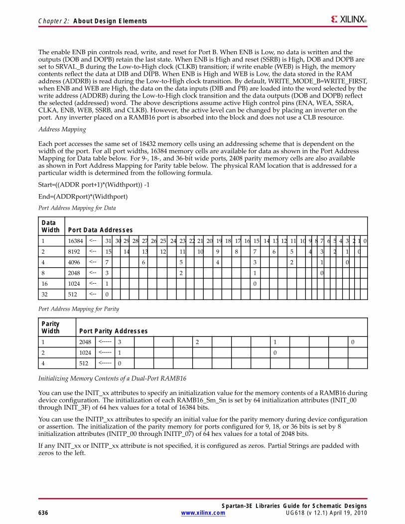
Chapter 2: About Design Elements
The enable ENB pin controls read, write, and reset for Port B. When ENB is Low, no data is written and theoutputs (DOB and DOPB) retain the last state. When ENB is High and reset (SSRB) is High, DOB and DOPB areset to SRVAL_B during the Low-to-High clock (CLKB) transition; if write enable (WEB) is High, the memorycontents reflect the data at DIB and DIPB. When ENB is High and WEB is Low, the data stored in the RAMaddress (ADDRB) is read during the Low-to-High clock transition. By default, WRITE_MODE_B=WRITE_FIRST,when ENB and WEB are High, the data on the data inputs (DIB and PB) are loaded into the word selected by thewrite address (ADDRB) during the Low-to-High clock transition and the data outputs (DOB and DOPB) reflectthe selected (addressed) word. The above descriptions assume active High control pins (ENA, WEA, SSRA,CLKA, ENB, WEB, SSRB, and CLKB). However, the active level can be changed by placing an inverter on theport. Any inverter placed on a RAMB16 port is absorbed into the block and does not use a CLB resource.
Address Mapping
Each port accesses the same set of 18432 memory cells using an addressing scheme that is dependent on thewidth of the port. For all port widths, 16384 memory cells are available for data as shown in the Port AddressMapping for Data table below. For 9-, 18-, and 36-bit wide ports, 2408 parity memory cells are also availableas shown in Port Address Mapping for Parity table below. The physical RAM location that is addressed for aparticular width is determined from the following formula.
Start=((ADDR port+1)*(Widthport)) -1
End=(ADDRport)*(Widthport)
Port Address Mapping for Data
DataWidth Port Data Addresses1 16384 <-- 31 30 29 28 27 26 25 24 23 22 21 20 19 18 17 16 15 14 13 12 11 10 9 8 7 6 5 4 3 2 1 0
2 8192 <-- 15 14 13 12 11 10 9 8 7 6 5 4 3 2 1 0
4 4096 <-- 7 6 5 4 3 2 1 0
8 2048 <-- 3 2 1 0
16 1024 <-- 1 0
32 512 <-- 0
Port Address Mapping for Parity
ParityWidth Port Parity Addresses1 2048 <----- 3 2 1 0
2 1024 <----- 1 0
4 512 <----- 0
Initializing Memory Contents of a Dual-Port RAMB16
You can use the INIT_xx attributes to specify an initialization value for the memory contents of a RAMB16 duringdevice configuration. The initialization of each RAMB16_Sm_Sn is set by 64 initialization attributes (INIT_00through INIT_3F) of 64 hex values for a total of 16384 bits.
You can use the INITP_xx attributes to specify an initial value for the parity memory during device configurationor assertion. The initialization of the parity memory for ports configured for 9, 18, or 36 bits is set by 8initialization attributes (INITP_00 through INITP_07) of 64 hex values for a total of 2048 bits.
If any INIT_xx or INITP_xx attribute is not specified, it is configured as zeros. Partial Strings are padded withzeros to the left.
Spartan-3E Libraries Guide for Schematic Designs636 www.xilinx.com UG618 (v 12.1) April 19, 2010
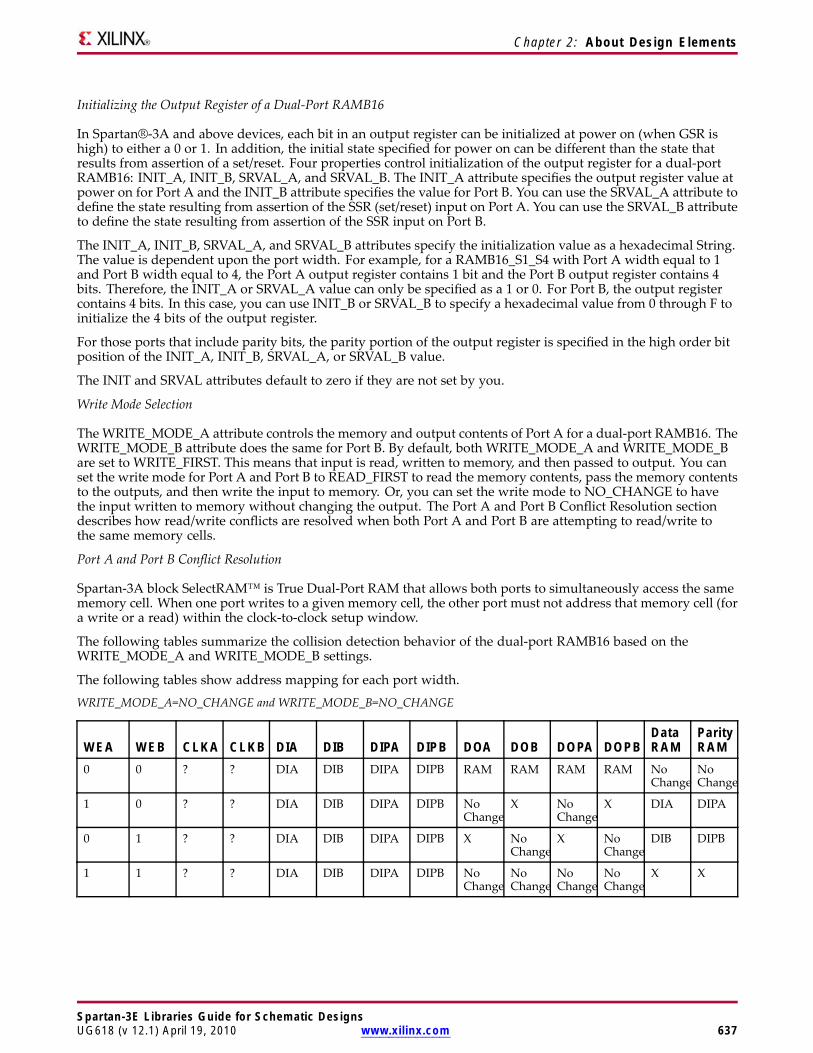
Chapter 2: About Design Elements
Initializing the Output Register of a Dual-Port RAMB16
In Spartan®-3A and above devices, each bit in an output register can be initialized at power on (when GSR ishigh) to either a 0 or 1. In addition, the initial state specified for power on can be different than the state thatresults from assertion of a set/reset. Four properties control initialization of the output register for a dual-portRAMB16: INIT_A, INIT_B, SRVAL_A, and SRVAL_B. The INIT_A attribute specifies the output register value atpower on for Port A and the INIT_B attribute specifies the value for Port B. You can use the SRVAL_A attribute todefine the state resulting from assertion of the SSR (set/reset) input on Port A. You can use the SRVAL_B attributeto define the state resulting from assertion of the SSR input on Port B.
The INIT_A, INIT_B, SRVAL_A, and SRVAL_B attributes specify the initialization value as a hexadecimal String.The value is dependent upon the port width. For example, for a RAMB16_S1_S4 with Port A width equal to 1and Port B width equal to 4, the Port A output register contains 1 bit and the Port B output register contains 4bits. Therefore, the INIT_A or SRVAL_A value can only be specified as a 1 or 0. For Port B, the output registercontains 4 bits. In this case, you can use INIT_B or SRVAL_B to specify a hexadecimal value from 0 through F toinitialize the 4 bits of the output register.
For those ports that include parity bits, the parity portion of the output register is specified in the high order bitposition of the INIT_A, INIT_B, SRVAL_A, or SRVAL_B value.
The INIT and SRVAL attributes default to zero if they are not set by you.
Write Mode Selection
TheWRITE_MODE_A attribute controls the memory and output contents of Port A for a dual-port RAMB16. TheWRITE_MODE_B attribute does the same for Port B. By default, both WRITE_MODE_A and WRITE_MODE_Bare set to WRITE_FIRST. This means that input is read, written to memory, and then passed to output. You canset the write mode for Port A and Port B to READ_FIRST to read the memory contents, pass the memory contentsto the outputs, and then write the input to memory. Or, you can set the write mode to NO_CHANGE to havethe input written to memory without changing the output. The Port A and Port B Conflict Resolution sectiondescribes how read/write conflicts are resolved when both Port A and Port B are attempting to read/write tothe same memory cells.
Port A and Port B Conflict Resolution
Spartan-3A block SelectRAM™ is True Dual-Port RAM that allows both ports to simultaneously access the samememory cell. When one port writes to a given memory cell, the other port must not address that memory cell (fora write or a read) within the clock-to-clock setup window.
The following tables summarize the collision detection behavior of the dual-port RAMB16 based on theWRITE_MODE_A and WRITE_MODE_B settings.
The following tables show address mapping for each port width.
WRITE_MODE_A=NO_CHANGE and WRITE_MODE_B=NO_CHANGE
WEA WEB CLKA CLKB DIA DIB DIPA DIPB DOA DOB DOPA DOPBDataRAM
ParityRAM
0 0 ? ? DIA DIB DIPA DIPB RAM RAM RAM RAM NoChange
NoChange
1 0 ? ? DIA DIB DIPA DIPB NoChange
X NoChange
X DIA DIPA
0 1 ? ? DIA DIB DIPA DIPB X NoChange
X NoChange
DIB DIPB
1 1 ? ? DIA DIB DIPA DIPB NoChange
NoChange
NoChange
NoChange
X X
Spartan-3E Libraries Guide for Schematic DesignsUG618 (v 12.1) April 19, 2010 www.xilinx.com 637
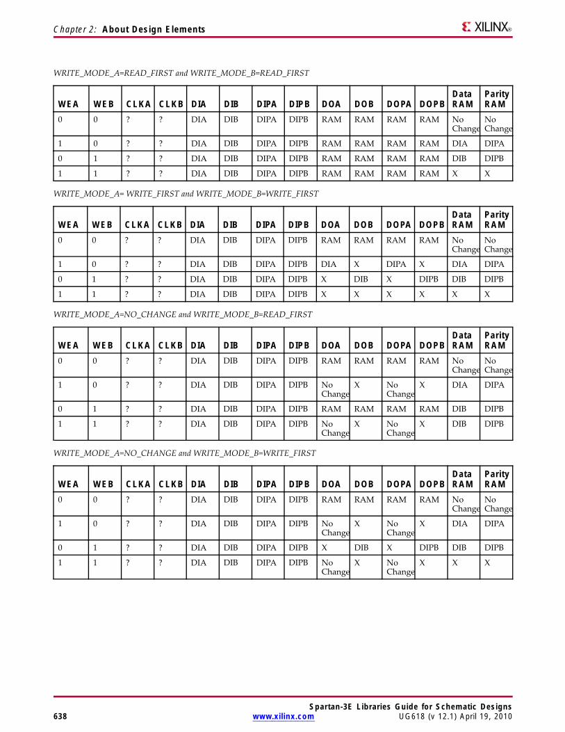
Chapter 2: About Design Elements
WRITE_MODE_A=READ_FIRST and WRITE_MODE_B=READ_FIRST
WEA WEB CLKA CLKB DIA DIB DIPA DIPB DOA DOB DOPA DOPBDataRAM
ParityRAM
0 0 ? ? DIA DIB DIPA DIPB RAM RAM RAM RAM NoChange
NoChange
1 0 ? ? DIA DIB DIPA DIPB RAM RAM RAM RAM DIA DIPA
0 1 ? ? DIA DIB DIPA DIPB RAM RAM RAM RAM DIB DIPB
1 1 ? ? DIA DIB DIPA DIPB RAM RAM RAM RAM X X
WRITE_MODE_A= WRITE_FIRST and WRITE_MODE_B=WRITE_FIRST
WEA WEB CLKA CLKB DIA DIB DIPA DIPB DOA DOB DOPA DOPBDataRAM
ParityRAM
0 0 ? ? DIA DIB DIPA DIPB RAM RAM RAM RAM NoChange
NoChange
1 0 ? ? DIA DIB DIPA DIPB DIA X DIPA X DIA DIPA
0 1 ? ? DIA DIB DIPA DIPB X DIB X DIPB DIB DIPB
1 1 ? ? DIA DIB DIPA DIPB X X X X X X
WRITE_MODE_A=NO_CHANGE and WRITE_MODE_B=READ_FIRST
WEA WEB CLKA CLKB DIA DIB DIPA DIPB DOA DOB DOPA DOPBDataRAM
ParityRAM
0 0 ? ? DIA DIB DIPA DIPB RAM RAM RAM RAM NoChange
NoChange
1 0 ? ? DIA DIB DIPA DIPB NoChange
X NoChange
X DIA DIPA
0 1 ? ? DIA DIB DIPA DIPB RAM RAM RAM RAM DIB DIPB
1 1 ? ? DIA DIB DIPA DIPB NoChange
X NoChange
X DIB DIPB
WRITE_MODE_A=NO_CHANGE and WRITE_MODE_B=WRITE_FIRST
WEA WEB CLKA CLKB DIA DIB DIPA DIPB DOA DOB DOPA DOPBDataRAM
ParityRAM
0 0 ? ? DIA DIB DIPA DIPB RAM RAM RAM RAM NoChange
NoChange
1 0 ? ? DIA DIB DIPA DIPB NoChange
X NoChange
X DIA DIPA
0 1 ? ? DIA DIB DIPA DIPB X DIB X DIPB DIB DIPB
1 1 ? ? DIA DIB DIPA DIPB NoChange
X NoChange
X X X
Spartan-3E Libraries Guide for Schematic Designs638 www.xilinx.com UG618 (v 12.1) April 19, 2010

Chapter 2: About Design Elements
WRITE_MODE_A=READ_FIRST and WRITE_MODE_B=WRITE_FIRST
WEA WEB CLKA CLKB DIA DIB DIPA DIPB DOA DOB DOPA DOPBDataRAM
ParityRAM
0 0 ? ? DIA DIB DIPA DIPB RAM RAM RAM RAM NoChange
NoChange
1 0 ? ? DIA DIB DIPA DIPB RAM RAM RAM RAM DIA DIPA
0 1 ? ? DIA DIB DIPA DIPB X DIB X DIPB DIB DIPB
1 1 ? ? DIA DIB DIPA DIPB X DIB X DIPB DIA DIPA
Design Entry MethodThis design element can be used in schematics.
Available Attributes
Attribute TypeAllowedValues Default Description
INIT_00 toINIT_3F
Binary/Hexadecimal
Any All zeros Specifies the initial contents of the data portionof the RAM array.
INIT_A Binary/Hexadecimal
Any All zeros Identifies the initial value of the DOA/DOB outputport after completing configuration. For Type, thebit width is dependent on the width of the A or Bport of the RAM.
INIT_B Binary/Hexadecimal
Any All zeros Identifies the initial value of the DOA/DOB outputport after completing configuration. For Type, thebit width is dependent on the width of the A or Bport of the RAM.
INITP_00 toINITP_07
Binary/Hexadecimal
Any All zeros Specifies the initial contents of the parity portionof the RAM array.
SIM_COLLISION_CHECK
String "ALL,WARNING_ONLY,"GENERATE_X_ONLY,NONE
"ALL Allows modification of the simulation behavior ifa memory collision occurs. The output is affectedas follows:
• "ALL" - Warning produced and affectedoutputs/memory location go unknown (X).
• "WARNING_ONLY" - Warning produced andaffected outputs/memory retain last value.
• "GENERATE_X_ONLY" - No warning.However, affected outputs/memory gounknown (X).
• "NONE" - No warning and affectedoutputs/memory retain last value.
Note Setting this to a value other than "ALL" canallow problems in the design go unnoticed duringsimulation. Care should be taken when changingthe value of this attribute. Please see the Synthesisand Simulation Design Guide for more information.
SRVAL_A Binary/Hexadecimal
Any All zeros Allows the individual selection of whether theDOA/DOB output port sets (go to a one) or reset(go to a zero) upon the assertion of the RSTA pin.For Type, the bit width is dependent on the widthof the A port of the RAM.
Spartan-3E Libraries Guide for Schematic DesignsUG618 (v 12.1) April 19, 2010 www.xilinx.com 639

Chapter 2: About Design Elements
Attribute TypeAllowedValues Default Description
SRVAL_B Binary/Hexadecimal
Any All zeros Allows the individual selection of whether theDOA/DOB output port sets (go to a one) or reset(go to a zero) upon the assertion of the RSTB pin.For Type, the bit width is dependent on the widthof the B port of the RAM.
WRITE_MODE_A String "WRITE_FIRST","READ_FIRST","NO_CHANGE
"WRITE_FIRST
Specifies the behavior of the DOA/DOB port upona write command to the respected port. If set to"WRITE_FIRST", the same port that is writtento displays the contents of the written data tothe outputs upon completion of the operation."READ_FIRST" displays the prior contents of theRAM to the output port prior to writing the newdata. "NO_CHANGE" keeps the previous valueon the output port and wont update the outputport upon a write command. This is the suggestedmode if not using the read data from a particularport of the RAM.
WRITE_MODE_B String "WRITE_FIRST","READ_FIRST","NO_CHANGE
"WRITE_FIRST
Specifies the behavior of the DOA/DOB port upona write command to the respected port. If set to"WRITE_FIRST", the same port that is writtento displays the contents of the written data tothe outputs upon completion of the operation."READ_FIRST" displays the prior contents of theRAM to the output port prior to writing the newdata. "NO_CHANGE" keeps the previous valueon the output port and wont update the outputport upon a write command. This is the suggestedmode if not using the read data from a particularport of the RAM.
For More Information• See the Spartan-3 Generation FPGA User Guide.
• See the Spartan-3E FPGA Family Complete Data Sheet.
Spartan-3E Libraries Guide for Schematic Designs640 www.xilinx.com UG618 (v 12.1) April 19, 2010

Spartan-3E Libraries Guide for Schematic Designs641 www.xilinx.com UG618 (v 12.1) April 19, 2010
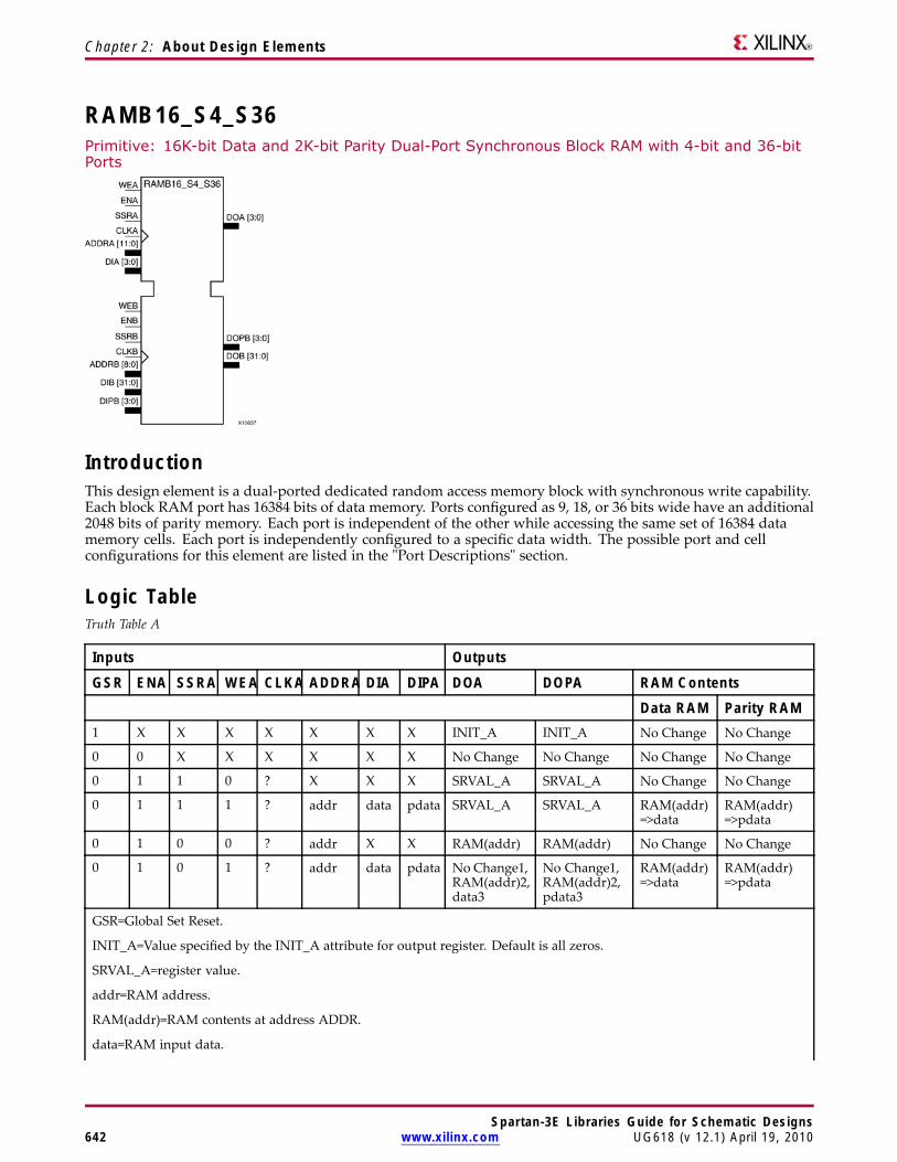
Chapter 2: About Design Elements
RAMB16_S4_S36Primitive: 16K-bit Data and 2K-bit Parity Dual-Port Synchronous Block RAM with 4-bit and 36-bitPorts
IntroductionThis design element is a dual-ported dedicated random access memory block with synchronous write capability.Each block RAM port has 16384 bits of data memory. Ports configured as 9, 18, or 36 bits wide have an additional2048 bits of parity memory. Each port is independent of the other while accessing the same set of 16384 datamemory cells. Each port is independently configured to a specific data width. The possible port and cellconfigurations for this element are listed in the "Port Descriptions" section.
Logic TableTruth Table A
Inputs Outputs
GSR ENA SSRA WEA CLKA ADDRA DIA DIPA DOA DOPA RAM ContentsData RAM Parity RAM
1 X X X X X X X INIT_A INIT_A No Change No Change
0 0 X X X X X X No Change No Change No Change No Change
0 1 1 0 ? X X X SRVAL_A SRVAL_A No Change No Change
0 1 1 1 ? addr data pdata SRVAL_A SRVAL_A RAM(addr)=>data
RAM(addr)=>pdata
0 1 0 0 ? addr X X RAM(addr) RAM(addr) No Change No Change
0 1 0 1 ? addr data pdata No Change1,RAM(addr)2,data3
No Change1,RAM(addr)2,pdata3
RAM(addr)=>data
RAM(addr)=>pdata
GSR=Global Set Reset.
INIT_A=Value specified by the INIT_A attribute for output register. Default is all zeros.
SRVAL_A=register value.
addr=RAM address.
RAM(addr)=RAM contents at address ADDR.
data=RAM input data.
Spartan-3E Libraries Guide for Schematic Designs642 www.xilinx.com UG618 (v 12.1) April 19, 2010
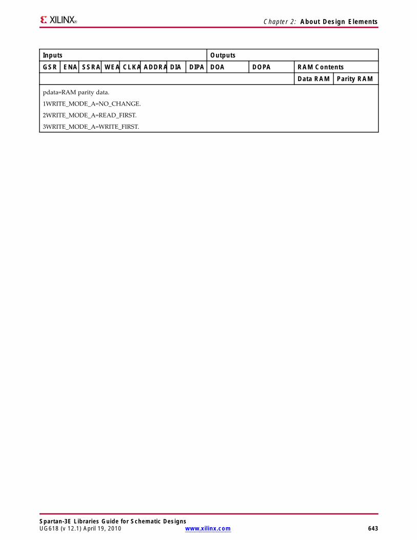
Chapter 2: About Design Elements
Inputs Outputs
GSR ENA SSRA WEA CLKA ADDRA DIA DIPA DOA DOPA RAM ContentsData RAM Parity RAM
pdata=RAM parity data.
1WRITE_MODE_A=NO_CHANGE.
2WRITE_MODE_A=READ_FIRST.
3WRITE_MODE_A=WRITE_FIRST.
Spartan-3E Libraries Guide for Schematic DesignsUG618 (v 12.1) April 19, 2010 www.xilinx.com 643
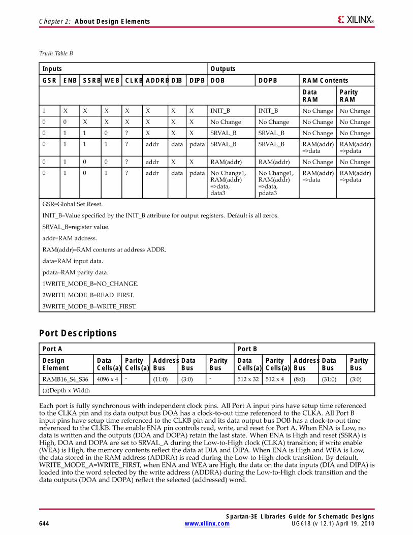
Chapter 2: About Design Elements
Truth Table B
Inputs Outputs
GSR ENB SSRB WEB CLKB ADDRB DIB DIPB DOB DOPB RAM ContentsDataRAM
ParityRAM
1 X X X X X X X INIT_B INIT_B No Change No Change
0 0 X X X X X X No Change No Change No Change No Change
0 1 1 0 ? X X X SRVAL_B SRVAL_B No Change No Change
0 1 1 1 ? addr data pdata SRVAL_B SRVAL_B RAM(addr)=>data
RAM(addr)=>pdata
0 1 0 0 ? addr X X RAM(addr) RAM(addr) No Change No Change
0 1 0 1 ? addr data pdata No Change1,RAM(addr)=>data,data3
No Change1,RAM(addr)=>data,pdata3
RAM(addr)=>data
RAM(addr)=>pdata
GSR=Global Set Reset.
INIT_B=Value specified by the INIT_B attribute for output registers. Default is all zeros.
SRVAL_B=register value.
addr=RAM address.
RAM(addr)=RAM contents at address ADDR.
data=RAM input data.
pdata=RAM parity data.
1WRITE_MODE_B=NO_CHANGE.
2WRITE_MODE_B=READ_FIRST.
3WRITE_MODE_B=WRITE_FIRST.
Port DescriptionsPort A Port BDesignElement
DataCells(a)
ParityCells(a)
AddressBus
DataBus
ParityBus
DataCells(a)
ParityCells(a)
AddressBus
DataBus
ParityBus
RAMB16_S4_S36 4096 x 4 - (11:0) (3:0) - 512 x 32 512 x 4 (8:0) (31:0) (3:0)
(a)Depth x Width
Each port is fully synchronous with independent clock pins. All Port A input pins have setup time referencedto the CLKA pin and its data output bus DOA has a clock-to-out time referenced to the CLKA. All Port Binput pins have setup time referenced to the CLKB pin and its data output bus DOB has a clock-to-out timereferenced to the CLKB. The enable ENA pin controls read, write, and reset for Port A. When ENA is Low, nodata is written and the outputs (DOA and DOPA) retain the last state. When ENA is High and reset (SSRA) isHigh, DOA and DOPA are set to SRVAL_A during the Low-to-High clock (CLKA) transition; if write enable(WEA) is High, the memory contents reflect the data at DIA and DIPA. When ENA is High and WEA is Low,the data stored in the RAM address (ADDRA) is read during the Low-to-High clock transition. By default,WRITE_MODE_A=WRITE_FIRST, when ENA and WEA are High, the data on the data inputs (DIA and DIPA) isloaded into the word selected by the write address (ADDRA) during the Low-to-High clock transition and thedata outputs (DOA and DOPA) reflect the selected (addressed) word.
Spartan-3E Libraries Guide for Schematic Designs644 www.xilinx.com UG618 (v 12.1) April 19, 2010

Chapter 2: About Design Elements
The enable ENB pin controls read, write, and reset for Port B. When ENB is Low, no data is written and theoutputs (DOB and DOPB) retain the last state. When ENB is High and reset (SSRB) is High, DOB and DOPB areset to SRVAL_B during the Low-to-High clock (CLKB) transition; if write enable (WEB) is High, the memorycontents reflect the data at DIB and DIPB. When ENB is High and WEB is Low, the data stored in the RAMaddress (ADDRB) is read during the Low-to-High clock transition. By default, WRITE_MODE_B=WRITE_FIRST,when ENB and WEB are High, the data on the data inputs (DIB and PB) are loaded into the word selected by thewrite address (ADDRB) during the Low-to-High clock transition and the data outputs (DOB and DOPB) reflectthe selected (addressed) word. The above descriptions assume active High control pins (ENA, WEA, SSRA,CLKA, ENB, WEB, SSRB, and CLKB). However, the active level can be changed by placing an inverter on theport. Any inverter placed on a RAMB16 port is absorbed into the block and does not use a CLB resource.
Address Mapping
Each port accesses the same set of 18432 memory cells using an addressing scheme that is dependent on thewidth of the port. For all port widths, 16384 memory cells are available for data as shown in the Port AddressMapping for Data table below. For 9-, 18-, and 36-bit wide ports, 2408 parity memory cells are also availableas shown in Port Address Mapping for Parity table below. The physical RAM location that is addressed for aparticular width is determined from the following formula.
Start=((ADDR port+1)*(Widthport)) -1
End=(ADDRport)*(Widthport)
The following tables shows address mapping for each port width.
Port Address Mapping for Data
DataWidth Port Data Addresses1 16384 <-- 31 30 29 28 27 26 25 24 23 22 21 20 19 18 17 16 15 14 13 12 11 10 9 8 7 6 5 4 3 2 1 0
2 8192 <-- 15 14 13 12 11 10 9 8 7 6 5 4 3 2 1 0
4 4096 <-- 7 6 5 4 3 2 1 0
8 2048 <-- 3 2 1 0
16 1024 <-- 1 0
32 512 <-- 0
Port Address Mapping for Parity
ParityWidth Port Parity Addresses1 2048 <----- 3 2 1 0
2 1024 <----- 1 0
4 512 <----- 0
Initializing Memory Contents of a Dual-Port RAMB16
You can use the INIT_xx attributes to specify an initialization value for the memory contents of a RAMB16 duringdevice configuration. The initialization of each RAMB16_Sm_Sn is set by 64 initialization attributes (INIT_00through INIT_3F) of 64 hex values for a total of 16384 bits.
You can use the INITP_xx attributes to specify an initial value for the parity memory during device configurationor assertion. The initialization of the parity memory for ports configured for 9, 18, or 36 bits is set by 8initialization attributes (INITP_00 through INITP_07) of 64 hex values for a total of 2048 bits.
If any INIT_xx or INITP_xx attribute is not specified, it is configured as zeros. Partial Strings are padded withzeros to the left.
Initializing the Output Register of a Dual-Port RAMB16
Spartan-3E Libraries Guide for Schematic DesignsUG618 (v 12.1) April 19, 2010 www.xilinx.com 645

Chapter 2: About Design Elements
In Spartan®-3A and above devices, each bit in an output register can be initialized at power on (when GSR ishigh) to either a 0 or 1. In addition, the initial state specified for power on can be different than the state thatresults from assertion of a set/reset. Four properties control initialization of the output register for a dual-portRAMB16: INIT_A, INIT_B, SRVAL_A, and SRVAL_B. The INIT_A attribute specifies the output register value atpower on for Port A and the INIT_B attribute specifies the value for Port B. You can use the SRVAL_A attribute todefine the state resulting from assertion of the SSR (set/reset) input on Port A. You can use the SRVAL_B attributeto define the state resulting from assertion of the SSR input on Port B.
The INIT_A, INIT_B, SRVAL_A, and SRVAL_B attributes specify the initialization value as a hexadecimal String.The value is dependent upon the port width. For example, for a RAMB16_S1_S4 with Port A width equal to 1and Port B width equal to 4, the Port A output register contains 1 bit and the Port B output register contains 4bits. Therefore, the INIT_A or SRVAL_A value can only be specified as a 1 or 0. For Port B, the output registercontains 4 bits. In this case, you can use INIT_B or SRVAL_B to specify a hexadecimal value from 0 through F toinitialize the 4 bits of the output register.
For those ports that include parity bits, the parity portion of the output register is specified in the high order bitposition of the INIT_A, INIT_B, SRVAL_A, or SRVAL_B value.
The INIT and SRVAL attributes default to zero if they are not set by you.
Write Mode Selection
TheWRITE_MODE_A attribute controls the memory and output contents of Port A for a dual-port RAMB16. TheWRITE_MODE_B attribute does the same for Port B. By default, both WRITE_MODE_A and WRITE_MODE_Bare set to WRITE_FIRST. This means that input is read, written to memory, and then passed to output. You canset the write mode for Port A and Port B to READ_FIRST to read the memory contents, pass the memory contentsto the outputs, and then write the input to memory. Or, you can set the write mode to NO_CHANGE to havethe input written to memory without changing the output. The Port A and Port B Conflict Resolution sectiondescribes how read/write conflicts are resolved when both Port A and Port B are attempting to read/write tothe same memory cells.
Port A and Port B Conflict Resolution
Spartan-3A block SelectRAM™ is True Dual-Port RAM that allows both ports to simultaneously access the samememory cell. When one port writes to a given memory cell, the other port must not address that memory cell (fora write or a read) within the clock-to-clock setup window.
The following tables summarize the collision detection behavior of the dual-port RAMB16 based on theWRITE_MODE_A and WRITE_MODE_B settings.
WRITE_MODE_A=NO_CHANGE and WRITE_MODE_B=NO_CHANGE
WEA WEB CLKA CLKB DIA DIB DIPA DIPB DOA DOB DOPA DOPBDataRAM
ParityRAM
0 0 ? ? DIA DIB DIPA DIPB RAM RAM RAM RAM NoChange
NoChange
1 0 ? ? DIA DIB DIPA DIPB NoChange
X NoChange
X DIA DIPA
0 1 ? ? DIA DIB DIPA DIPB X NoChange
X NoChange
DIB DIPB
1 1 ? ? DIA DIB DIPA DIPB NoChange
NoChange
NoChange
NoChange
X X
WRITE_MODE_A=READ_FIRST and WRITE_MODE_B=READ_FIRST
Spartan-3E Libraries Guide for Schematic Designs646 www.xilinx.com UG618 (v 12.1) April 19, 2010

Chapter 2: About Design Elements
WEA WEB CLKA CLKB DIA DIB DIPA DIPB DOA DOB DOPA DOPBDataRAM
ParityRAM
0 0 ? ? DIA DIB DIPA DIPB RAM RAM RAM RAM NoChange
NoChange
1 0 ? ? DIA DIB DIPA DIPB RAM RAM RAM RAM DIA DIPA
0 1 ? ? DIA DIB DIPA DIPB RAM RAM RAM RAM DIB DIPB
1 1 ? ? DIA DIB DIPA DIPB RAM RAM RAM RAM X X
WRITE_MODE_A= WRITE_FIRST and WRITE_MODE_B=WRITE_FIRST
WEA WEB CLKA CLKB DIA DIB DIPA DIPB DOA DOB DOPA DOPBDataRAM
ParityRAM
0 0 ? ? DIA DIB DIPA DIPB RAM RAM RAM RAM NoChange
NoChange
1 0 ? ? DIA DIB DIPA DIPB DIA X DIPA X DIA DIPA
0 1 ? ? DIA DIB DIPA DIPB X DIB X DIPB DIB DIPB
1 1 ? ? DIA DIB DIPA DIPB X X X X X X
WRITE_MODE_A=NO_CHANGE and WRITE_MODE_B=READ_FIRST
WEA WEB CLKA CLKB DIA DIB DIPA DIPB DOA DOB DOPA DOPBDataRAM
ParityRAM
0 0 ? ? DIA DIB DIPA DIPB RAM RAM RAM RAM NoChange
NoChange
1 0 ? ? DIA DIB DIPA DIPB NoChange
X NoChange
X DIA DIPA
0 1 ? ? DIA DIB DIPA DIPB RAM RAM RAM RAM DIB DIPB
1 1 ? ? DIA DIB DIPA DIPB NoChange
X NoChange
X DIB DIPB
WRITE_MODE_A=NO_CHANGE and WRITE_MODE_B=WRITE_FIRST
WEA WEB CLKA CLKB DIA DIB DIPA DIPB DOA DOB DOPA DOPBDataRAM
ParityRAM
0 0 ? ? DIA DIB DIPA DIPB RAM RAM RAM RAM NoChange
NoChange
1 0 ? ? DIA DIB DIPA DIPB NoChange
X NoChange
X DIA DIPA
0 1 ? ? DIA DIB DIPA DIPB X DIB X DIPB DIB DIPB
1 1 ? ? DIA DIB DIPA DIPB NoChange
X NoChange
X X X
WRITE_MODE_A=READ_FIRST and WRITE_MODE_B=WRITE_FIRST
WEA WEB CLKA CLKB DIA DIB DIPA DIPB DOA DOB DOPA DOPBDataRAM
ParityRAM
0 0 ? ? DIA DIB DIPA DIPB RAM RAM RAM RAM NoChange
NoChange
1 0 ? ? DIA DIB DIPA DIPB RAM RAM RAM RAM DIA DIPA
0 1 ? ? DIA DIB DIPA DIPB X DIB X DIPB DIB DIPB
1 1 ? ? DIA DIB DIPA DIPB X DIB X DIPB DIA DIPA
Spartan-3E Libraries Guide for Schematic DesignsUG618 (v 12.1) April 19, 2010 www.xilinx.com 647
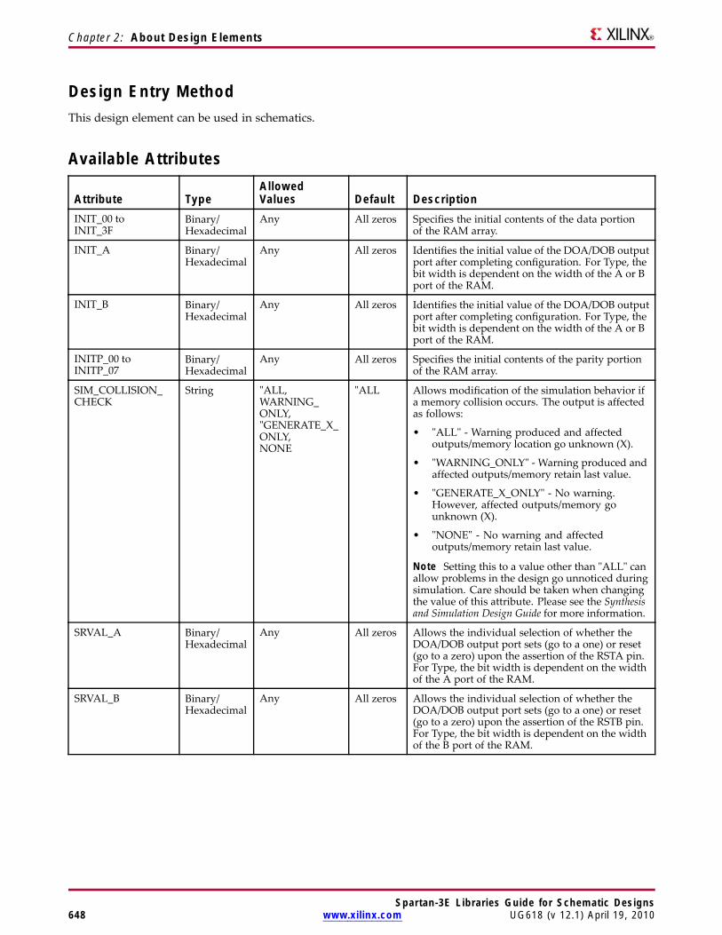
Chapter 2: About Design Elements
Design Entry MethodThis design element can be used in schematics.
Available Attributes
Attribute TypeAllowedValues Default Description
INIT_00 toINIT_3F
Binary/Hexadecimal
Any All zeros Specifies the initial contents of the data portionof the RAM array.
INIT_A Binary/Hexadecimal
Any All zeros Identifies the initial value of the DOA/DOB outputport after completing configuration. For Type, thebit width is dependent on the width of the A or Bport of the RAM.
INIT_B Binary/Hexadecimal
Any All zeros Identifies the initial value of the DOA/DOB outputport after completing configuration. For Type, thebit width is dependent on the width of the A or Bport of the RAM.
INITP_00 toINITP_07
Binary/Hexadecimal
Any All zeros Specifies the initial contents of the parity portionof the RAM array.
SIM_COLLISION_CHECK
String "ALL,WARNING_ONLY,"GENERATE_X_ONLY,NONE
"ALL Allows modification of the simulation behavior ifa memory collision occurs. The output is affectedas follows:
• "ALL" - Warning produced and affectedoutputs/memory location go unknown (X).
• "WARNING_ONLY" - Warning produced andaffected outputs/memory retain last value.
• "GENERATE_X_ONLY" - No warning.However, affected outputs/memory gounknown (X).
• "NONE" - No warning and affectedoutputs/memory retain last value.
Note Setting this to a value other than "ALL" canallow problems in the design go unnoticed duringsimulation. Care should be taken when changingthe value of this attribute. Please see the Synthesisand Simulation Design Guide for more information.
SRVAL_A Binary/Hexadecimal
Any All zeros Allows the individual selection of whether theDOA/DOB output port sets (go to a one) or reset(go to a zero) upon the assertion of the RSTA pin.For Type, the bit width is dependent on the widthof the A port of the RAM.
SRVAL_B Binary/Hexadecimal
Any All zeros Allows the individual selection of whether theDOA/DOB output port sets (go to a one) or reset(go to a zero) upon the assertion of the RSTB pin.For Type, the bit width is dependent on the widthof the B port of the RAM.
Spartan-3E Libraries Guide for Schematic Designs648 www.xilinx.com UG618 (v 12.1) April 19, 2010

Chapter 2: About Design Elements
Attribute TypeAllowedValues Default Description
WRITE_MODE_A String "WRITE_FIRST","READ_FIRST","NO_CHANGE
"WRITE_FIRST
Specifies the behavior of the DOA/DOB port upona write command to the respected port. If set to"WRITE_FIRST", the same port that is writtento displays the contents of the written data tothe outputs upon completion of the operation."READ_FIRST" displays the prior contents of theRAM to the output port prior to writing the newdata. "NO_CHANGE" keeps the previous valueon the output port and wont update the outputport upon a write command. This is the suggestedmode if not using the read data from a particularport of the RAM.
WRITE_MODE_B String "WRITE_FIRST","READ_FIRST","NO_CHANGE
"WRITE_FIRST
Specifies the behavior of the DOA/DOB port upona write command to the respected port. If set to"WRITE_FIRST", the same port that is writtento displays the contents of the written data tothe outputs upon completion of the operation."READ_FIRST" displays the prior contents of theRAM to the output port prior to writing the newdata. "NO_CHANGE" keeps the previous valueon the output port and wont update the outputport upon a write command. This is the suggestedmode if not using the read data from a particularport of the RAM.
For More Information• See the Spartan-3 Generation FPGA User Guide.
• See the Spartan-3E FPGA Family Complete Data Sheet.
Spartan-3E Libraries Guide for Schematic DesignsUG618 (v 12.1) April 19, 2010 www.xilinx.com 649

Spartan-3E Libraries Guide for Schematic Designs650 www.xilinx.com UG618 (v 12.1) April 19, 2010
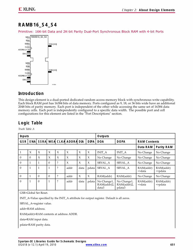
Chapter 2: About Design Elements
RAMB16_S4_S4Primitive: 16K-bit Data and 2K-bit Parity Dual-Port Synchronous Block RAM with 4-bit Ports
IntroductionThis design element is a dual-ported dedicated random access memory block with synchronous write capability.Each block RAM port has 16384 bits of data memory. Ports configured as 9, 18, or 36 bits wide have an additional2048 bits of parity memory. Each port is independent of the other while accessing the same set of 16384 datamemory cells. Each port is independently configured to a specific data width. The possible port and cellconfigurations for this element are listed in the "Port Descriptions" section.
Logic TableTruth Table A
Inputs Outputs
GSR ENA SSRA WEA CLKA ADDRA DIA DIPA DOA DOPA RAM ContentsData RAM Parity RAM
1 X X X X X X X INIT_A INIT_A No Change No Change
0 0 X X X X X X No Change No Change No Change No Change
0 1 1 0 ? X X X SRVAL_A SRVAL_A No Change No Change
0 1 1 1 ? addr data pdata SRVAL_A SRVAL_A RAM(addr)=>data
RAM(addr)=>pdata
0 1 0 0 ? addr X X RAM(addr) RAM(addr) No Change No Change
0 1 0 1 ? addr data pdata No Change1,RAM(addr)2,data3
No Change1,RAM(addr)2,pdata3
RAM(addr)=>data
RAM(addr)=>pdata
GSR=Global Set Reset.
INIT_A=Value specified by the INIT_A attribute for output register. Default is all zeros.
SRVAL_A=register value.
addr=RAM address.
RAM(addr)=RAM contents at address ADDR.
data=RAM input data.
pdata=RAM parity data.
Spartan-3E Libraries Guide for Schematic DesignsUG618 (v 12.1) April 19, 2010 www.xilinx.com 651
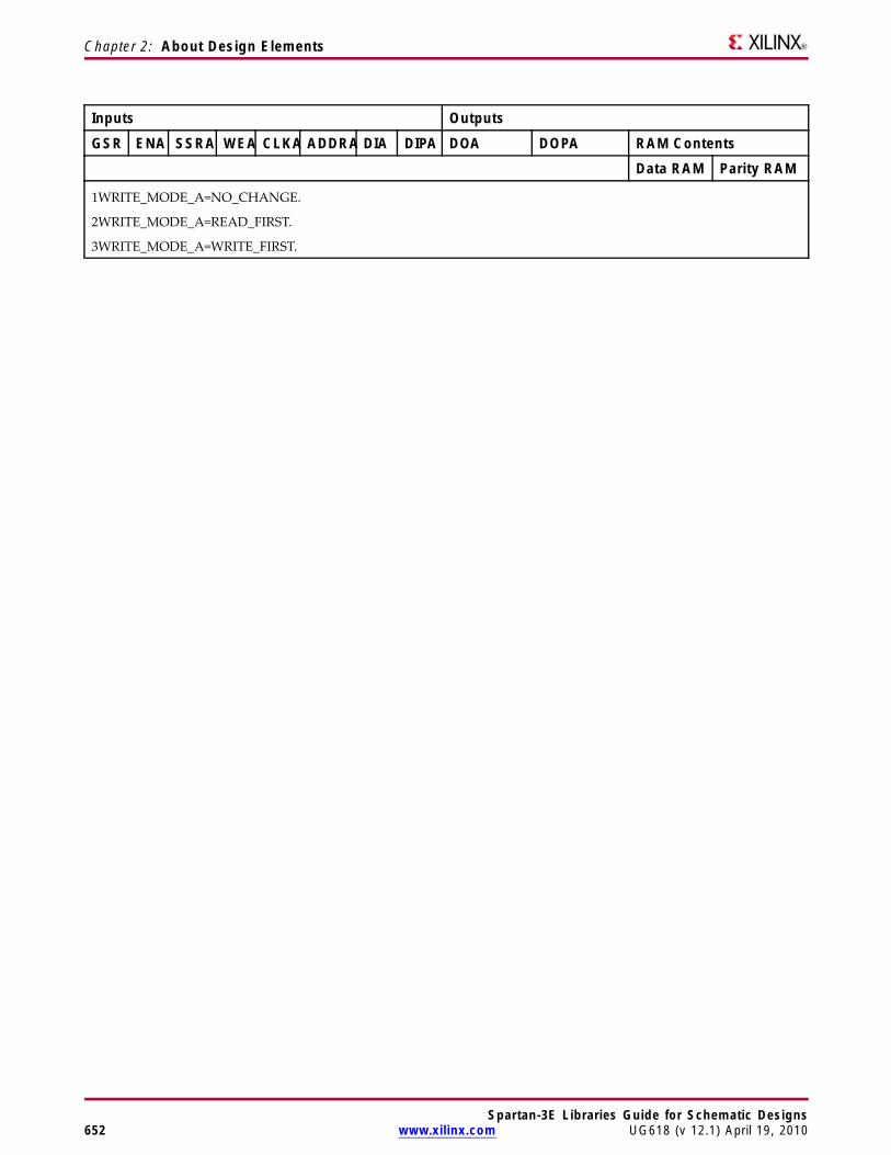
Chapter 2: About Design Elements
Inputs Outputs
GSR ENA SSRA WEA CLKA ADDRA DIA DIPA DOA DOPA RAM ContentsData RAM Parity RAM
1WRITE_MODE_A=NO_CHANGE.
2WRITE_MODE_A=READ_FIRST.
3WRITE_MODE_A=WRITE_FIRST.
Spartan-3E Libraries Guide for Schematic Designs652 www.xilinx.com UG618 (v 12.1) April 19, 2010

Chapter 2: About Design Elements
Truth Table B
Inputs Outputs
GSR ENB SSRB WEB CLKB ADDRB DIB DIPB DOB DOPB RAM ContentsDataRAM
ParityRAM
1 X X X X X X X INIT_B INIT_B No Change No Change
0 0 X X X X X X No Change No Change No Change No Change
0 1 1 0 ? X X X SRVAL_B SRVAL_B No Change No Change
0 1 1 1 ? addr data pdata SRVAL_B SRVAL_B RAM(addr)=>data
RAM(addr)=>pdata
0 1 0 0 ? addr X X RAM(addr) RAM(addr) No Change No Change
0 1 0 1 ? addr data pdata No Change1,RAM(addr)=>data,data3
No Change1,RAM(addr)=>data,pdata3
RAM(addr)=>data
RAM(addr)=>pdata
GSR=Global Set Reset.
INIT_B=Value specified by the INIT_B attribute for output registers. Default is all zeros.
SRVAL_B=register value.
addr=RAM address.
RAM(addr)=RAM contents at address ADDR.
data=RAM input data.
pdata=RAM parity data.
1WRITE_MODE_B=NO_CHANGE.
2WRITE_MODE_B=READ_FIRST.
3WRITE_MODE_B=WRITE_FIRST.
Port DescriptionsPort A Port BDesignElement
DataCells(a)
ParityCells(a)
AddressBus
DataBus
ParityBus
DataCells(a)
ParityCells(a)
AddressBus
DataBus
ParityBus
RAMB16_S4_S4 4096 x 4 - (11:0) (3:0) - 4096 x 4 - (11:0) (3:0) -
(a)Depth x Width
Each port is fully synchronous with independent clock pins. All Port A input pins have setup time referencedto the CLKA pin and its data output bus DOA has a clock-to-out time referenced to the CLKA. All Port Binput pins have setup time referenced to the CLKB pin and its data output bus DOB has a clock-to-out timereferenced to the CLKB. The enable ENA pin controls read, write, and reset for Port A. When ENA is Low, nodata is written and the outputs (DOA and DOPA) retain the last state. When ENA is High and reset (SSRA) isHigh, DOA and DOPA are set to SRVAL_A during the Low-to-High clock (CLKA) transition; if write enable(WEA) is High, the memory contents reflect the data at DIA and DIPA. When ENA is High and WEA is Low,the data stored in the RAM address (ADDRA) is read during the Low-to-High clock transition. By default,WRITE_MODE_A=WRITE_FIRST, when ENA and WEA are High, the data on the data inputs (DIA and DIPA) isloaded into the word selected by the write address (ADDRA) during the Low-to-High clock transition and thedata outputs (DOA and DOPA) reflect the selected (addressed) word.
Spartan-3E Libraries Guide for Schematic DesignsUG618 (v 12.1) April 19, 2010 www.xilinx.com 653
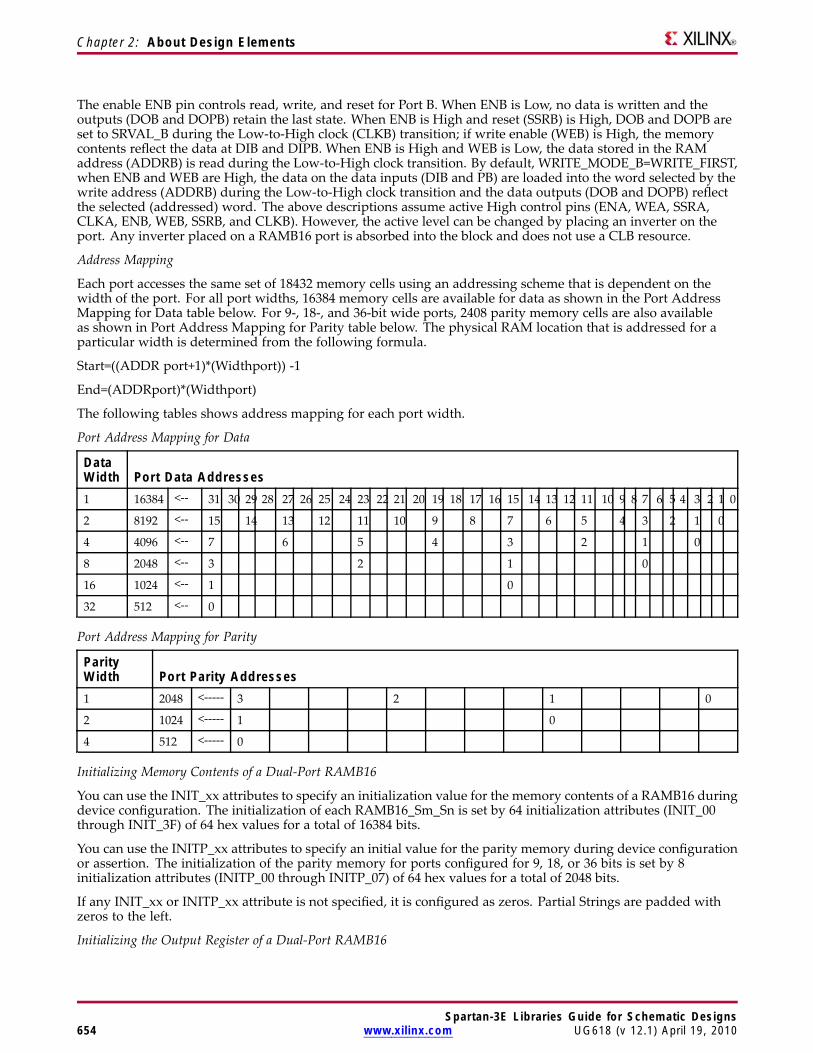
Chapter 2: About Design Elements
The enable ENB pin controls read, write, and reset for Port B. When ENB is Low, no data is written and theoutputs (DOB and DOPB) retain the last state. When ENB is High and reset (SSRB) is High, DOB and DOPB areset to SRVAL_B during the Low-to-High clock (CLKB) transition; if write enable (WEB) is High, the memorycontents reflect the data at DIB and DIPB. When ENB is High and WEB is Low, the data stored in the RAMaddress (ADDRB) is read during the Low-to-High clock transition. By default, WRITE_MODE_B=WRITE_FIRST,when ENB and WEB are High, the data on the data inputs (DIB and PB) are loaded into the word selected by thewrite address (ADDRB) during the Low-to-High clock transition and the data outputs (DOB and DOPB) reflectthe selected (addressed) word. The above descriptions assume active High control pins (ENA, WEA, SSRA,CLKA, ENB, WEB, SSRB, and CLKB). However, the active level can be changed by placing an inverter on theport. Any inverter placed on a RAMB16 port is absorbed into the block and does not use a CLB resource.
Address Mapping
Each port accesses the same set of 18432 memory cells using an addressing scheme that is dependent on thewidth of the port. For all port widths, 16384 memory cells are available for data as shown in the Port AddressMapping for Data table below. For 9-, 18-, and 36-bit wide ports, 2408 parity memory cells are also availableas shown in Port Address Mapping for Parity table below. The physical RAM location that is addressed for aparticular width is determined from the following formula.
Start=((ADDR port+1)*(Widthport)) -1
End=(ADDRport)*(Widthport)
The following tables shows address mapping for each port width.
Port Address Mapping for Data
DataWidth Port Data Addresses1 16384 <-- 31 30 29 28 27 26 25 24 23 22 21 20 19 18 17 16 15 14 13 12 11 10 9 8 7 6 5 4 3 2 1 0
2 8192 <-- 15 14 13 12 11 10 9 8 7 6 5 4 3 2 1 0
4 4096 <-- 7 6 5 4 3 2 1 0
8 2048 <-- 3 2 1 0
16 1024 <-- 1 0
32 512 <-- 0
Port Address Mapping for Parity
ParityWidth Port Parity Addresses1 2048 <----- 3 2 1 0
2 1024 <----- 1 0
4 512 <----- 0
Initializing Memory Contents of a Dual-Port RAMB16
You can use the INIT_xx attributes to specify an initialization value for the memory contents of a RAMB16 duringdevice configuration. The initialization of each RAMB16_Sm_Sn is set by 64 initialization attributes (INIT_00through INIT_3F) of 64 hex values for a total of 16384 bits.
You can use the INITP_xx attributes to specify an initial value for the parity memory during device configurationor assertion. The initialization of the parity memory for ports configured for 9, 18, or 36 bits is set by 8initialization attributes (INITP_00 through INITP_07) of 64 hex values for a total of 2048 bits.
If any INIT_xx or INITP_xx attribute is not specified, it is configured as zeros. Partial Strings are padded withzeros to the left.
Initializing the Output Register of a Dual-Port RAMB16
Spartan-3E Libraries Guide for Schematic Designs654 www.xilinx.com UG618 (v 12.1) April 19, 2010
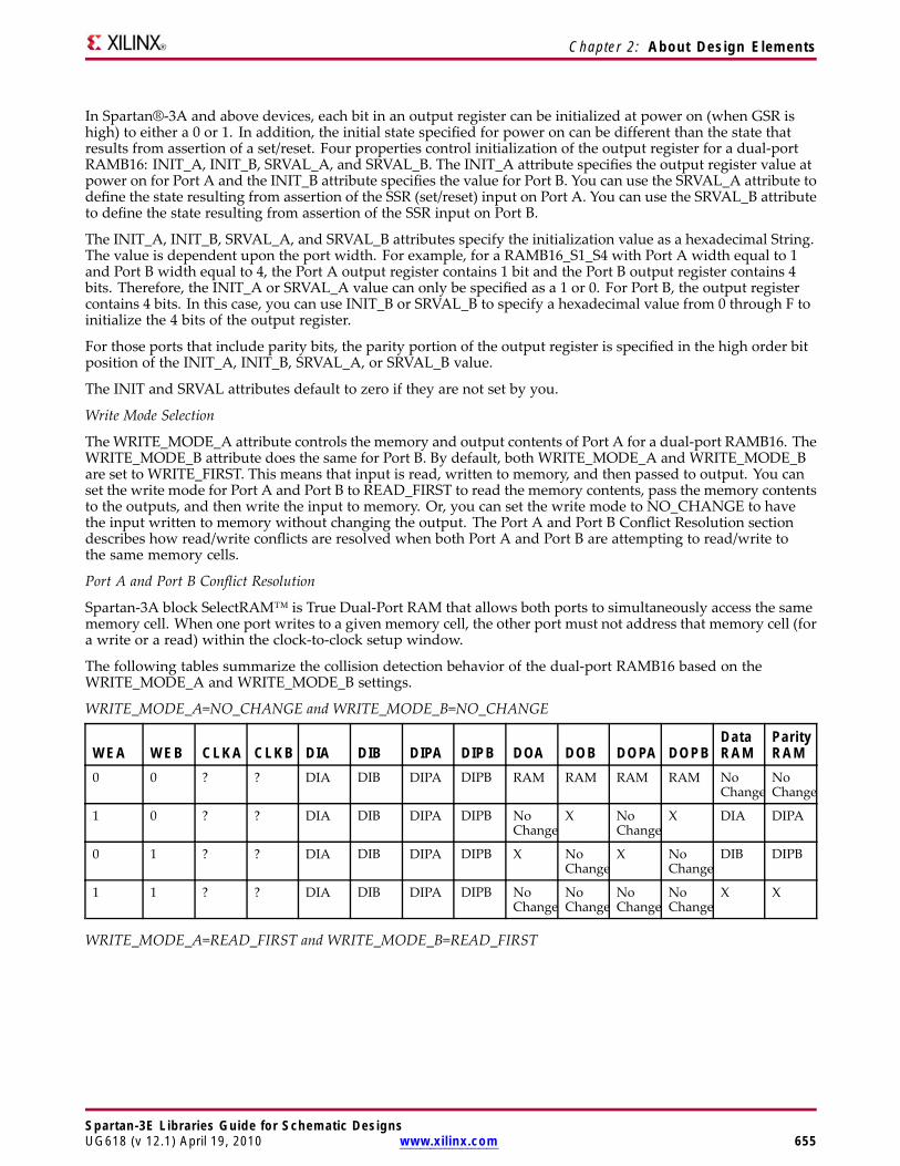
Chapter 2: About Design Elements
In Spartan®-3A and above devices, each bit in an output register can be initialized at power on (when GSR ishigh) to either a 0 or 1. In addition, the initial state specified for power on can be different than the state thatresults from assertion of a set/reset. Four properties control initialization of the output register for a dual-portRAMB16: INIT_A, INIT_B, SRVAL_A, and SRVAL_B. The INIT_A attribute specifies the output register value atpower on for Port A and the INIT_B attribute specifies the value for Port B. You can use the SRVAL_A attribute todefine the state resulting from assertion of the SSR (set/reset) input on Port A. You can use the SRVAL_B attributeto define the state resulting from assertion of the SSR input on Port B.
The INIT_A, INIT_B, SRVAL_A, and SRVAL_B attributes specify the initialization value as a hexadecimal String.The value is dependent upon the port width. For example, for a RAMB16_S1_S4 with Port A width equal to 1and Port B width equal to 4, the Port A output register contains 1 bit and the Port B output register contains 4bits. Therefore, the INIT_A or SRVAL_A value can only be specified as a 1 or 0. For Port B, the output registercontains 4 bits. In this case, you can use INIT_B or SRVAL_B to specify a hexadecimal value from 0 through F toinitialize the 4 bits of the output register.
For those ports that include parity bits, the parity portion of the output register is specified in the high order bitposition of the INIT_A, INIT_B, SRVAL_A, or SRVAL_B value.
The INIT and SRVAL attributes default to zero if they are not set by you.
Write Mode Selection
TheWRITE_MODE_A attribute controls the memory and output contents of Port A for a dual-port RAMB16. TheWRITE_MODE_B attribute does the same for Port B. By default, both WRITE_MODE_A and WRITE_MODE_Bare set to WRITE_FIRST. This means that input is read, written to memory, and then passed to output. You canset the write mode for Port A and Port B to READ_FIRST to read the memory contents, pass the memory contentsto the outputs, and then write the input to memory. Or, you can set the write mode to NO_CHANGE to havethe input written to memory without changing the output. The Port A and Port B Conflict Resolution sectiondescribes how read/write conflicts are resolved when both Port A and Port B are attempting to read/write tothe same memory cells.
Port A and Port B Conflict Resolution
Spartan-3A block SelectRAM™ is True Dual-Port RAM that allows both ports to simultaneously access the samememory cell. When one port writes to a given memory cell, the other port must not address that memory cell (fora write or a read) within the clock-to-clock setup window.
The following tables summarize the collision detection behavior of the dual-port RAMB16 based on theWRITE_MODE_A and WRITE_MODE_B settings.
WRITE_MODE_A=NO_CHANGE and WRITE_MODE_B=NO_CHANGE
WEA WEB CLKA CLKB DIA DIB DIPA DIPB DOA DOB DOPA DOPBDataRAM
ParityRAM
0 0 ? ? DIA DIB DIPA DIPB RAM RAM RAM RAM NoChange
NoChange
1 0 ? ? DIA DIB DIPA DIPB NoChange
X NoChange
X DIA DIPA
0 1 ? ? DIA DIB DIPA DIPB X NoChange
X NoChange
DIB DIPB
1 1 ? ? DIA DIB DIPA DIPB NoChange
NoChange
NoChange
NoChange
X X
WRITE_MODE_A=READ_FIRST and WRITE_MODE_B=READ_FIRST
Spartan-3E Libraries Guide for Schematic DesignsUG618 (v 12.1) April 19, 2010 www.xilinx.com 655

Chapter 2: About Design Elements
WEA WEB CLKA CLKB DIA DIB DIPA DIPB DOA DOB DOPA DOPBDataRAM
ParityRAM
0 0 ? ? DIA DIB DIPA DIPB RAM RAM RAM RAM NoChange
NoChange
1 0 ? ? DIA DIB DIPA DIPB RAM RAM RAM RAM DIA DIPA
0 1 ? ? DIA DIB DIPA DIPB RAM RAM RAM RAM DIB DIPB
1 1 ? ? DIA DIB DIPA DIPB RAM RAM RAM RAM X X
WRITE_MODE_A= WRITE_FIRST and WRITE_MODE_B=WRITE_FIRST
WEA WEB CLKA CLKB DIA DIB DIPA DIPB DOA DOB DOPA DOPBDataRAM
ParityRAM
0 0 ? ? DIA DIB DIPA DIPB RAM RAM RAM RAM NoChange
NoChange
1 0 ? ? DIA DIB DIPA DIPB DIA X DIPA X DIA DIPA
0 1 ? ? DIA DIB DIPA DIPB X DIB X DIPB DIB DIPB
1 1 ? ? DIA DIB DIPA DIPB X X X X X X
WRITE_MODE_A=NO_CHANGE and WRITE_MODE_B=READ_FIRST
WEA WEB CLKA CLKB DIA DIB DIPA DIPB DOA DOB DOPA DOPBDataRAM
ParityRAM
0 0 ? ? DIA DIB DIPA DIPB RAM RAM RAM RAM NoChange
NoChange
1 0 ? ? DIA DIB DIPA DIPB NoChange
X NoChange
X DIA DIPA
0 1 ? ? DIA DIB DIPA DIPB RAM RAM RAM RAM DIB DIPB
1 1 ? ? DIA DIB DIPA DIPB NoChange
X NoChange
X DIB DIPB
WRITE_MODE_A=NO_CHANGE and WRITE_MODE_B=WRITE_FIRST
WEA WEB CLKA CLKB DIA DIB DIPA DIPB DOA DOB DOPA DOPBDataRAM
ParityRAM
0 0 ? ? DIA DIB DIPA DIPB RAM RAM RAM RAM NoChange
NoChange
1 0 ? ? DIA DIB DIPA DIPB NoChange
X NoChange
X DIA DIPA
0 1 ? ? DIA DIB DIPA DIPB X DIB X DIPB DIB DIPB
1 1 ? ? DIA DIB DIPA DIPB NoChange
X NoChange
X X X
WRITE_MODE_A=READ_FIRST and WRITE_MODE_B=WRITE_FIRST
WEA WEB CLKA CLKB DIA DIB DIPA DIPB DOA DOB DOPA DOPBDataRAM
ParityRAM
0 0 ? ? DIA DIB DIPA DIPB RAM RAM RAM RAM NoChange
NoChange
1 0 ? ? DIA DIB DIPA DIPB RAM RAM RAM RAM DIA DIPA
0 1 ? ? DIA DIB DIPA DIPB X DIB X DIPB DIB DIPB
1 1 ? ? DIA DIB DIPA DIPB X DIB X DIPB DIA DIPA
Spartan-3E Libraries Guide for Schematic Designs656 www.xilinx.com UG618 (v 12.1) April 19, 2010
Chapter 2: About Design Elements
Design Entry MethodThis design element can be used in schematics.
Available Attributes
Attribute TypeAllowedValues Default Description
INIT_00 toINIT_3F
Binary/Hexadecimal
Any All zeros Specifies the initial contents of the data portionof the RAM array.
INIT_A Binary/Hexadecimal
Any All zeros Identifies the initial value of the DOA/DOB outputport after completing configuration. For Type, thebit width is dependent on the width of the A or Bport of the RAM.
INIT_B Binary/Hexadecimal
Any All zeros Identifies the initial value of the DOA/DOB outputport after completing configuration. For Type, thebit width is dependent on the width of the A or Bport of the RAM.
INITP_00 toINITP_07
Binary/Hexadecimal
Any All zeros Specifies the initial contents of the parity portionof the RAM array.
SIM_COLLISION_CHECK
String "ALL,WARNING_ONLY,"GENERATE_X_ONLY,NONE
"ALL Allows modification of the simulation behavior ifa memory collision occurs. The output is affectedas follows:
• "ALL" - Warning produced and affectedoutputs/memory location go unknown (X).
• "WARNING_ONLY" - Warning produced andaffected outputs/memory retain last value.
• "GENERATE_X_ONLY" - No warning.However, affected outputs/memory gounknown (X).
• "NONE" - No warning and affectedoutputs/memory retain last value.
Note Setting this to a value other than "ALL" canallow problems in the design go unnoticed duringsimulation. Care should be taken when changingthe value of this attribute. Please see the Synthesisand Simulation Design Guide for more information.
SRVAL_A Binary/Hexadecimal
Any All zeros Allows the individual selection of whether theDOA/DOB output port sets (go to a one) or reset(go to a zero) upon the assertion of the RSTA pin.For Type, the bit width is dependent on the widthof the A port of the RAM.
SRVAL_B Binary/Hexadecimal
Any All zeros Allows the individual selection of whether theDOA/DOB output port sets (go to a one) or reset(go to a zero) upon the assertion of the RSTB pin.For Type, the bit width is dependent on the widthof the B port of the RAM.
Spartan-3E Libraries Guide for Schematic DesignsUG618 (v 12.1) April 19, 2010 www.xilinx.com 657
Chapter 2: About Design Elements
Attribute TypeAllowedValues Default Description
WRITE_MODE_A String "WRITE_FIRST","READ_FIRST","NO_CHANGE
"WRITE_FIRST
Specifies the behavior of the DOA/DOB port upona write command to the respected port. If set to"WRITE_FIRST", the same port that is writtento displays the contents of the written data tothe outputs upon completion of the operation."READ_FIRST" displays the prior contents of theRAM to the output port prior to writing the newdata. "NO_CHANGE" keeps the previous valueon the output port and wont update the outputport upon a write command. This is the suggestedmode if not using the read data from a particularport of the RAM.
WRITE_MODE_B String "WRITE_FIRST","READ_FIRST","NO_CHANGE
"WRITE_FIRST
Specifies the behavior of the DOA/DOB port upona write command to the respected port. If set to"WRITE_FIRST", the same port that is writtento displays the contents of the written data tothe outputs upon completion of the operation."READ_FIRST" displays the prior contents of theRAM to the output port prior to writing the newdata. "NO_CHANGE" keeps the previous valueon the output port and wont update the outputport upon a write command. This is the suggestedmode if not using the read data from a particularport of the RAM.
For More Information• See the Spartan-3 Generation FPGA User Guide.
• See the Spartan-3E FPGA Family Complete Data Sheet.
Spartan-3E Libraries Guide for Schematic Designs658 www.xilinx.com UG618 (v 12.1) April 19, 2010

Spartan-3E Libraries Guide for Schematic Designs659 www.xilinx.com UG618 (v 12.1) April 19, 2010
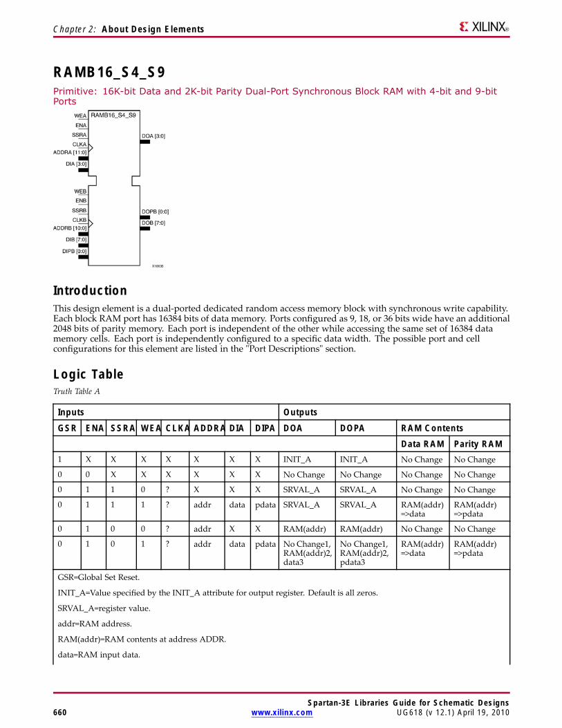
Chapter 2: About Design Elements
RAMB16_S4_S9Primitive: 16K-bit Data and 2K-bit Parity Dual-Port Synchronous Block RAM with 4-bit and 9-bitPorts
IntroductionThis design element is a dual-ported dedicated random access memory block with synchronous write capability.Each block RAM port has 16384 bits of data memory. Ports configured as 9, 18, or 36 bits wide have an additional2048 bits of parity memory. Each port is independent of the other while accessing the same set of 16384 datamemory cells. Each port is independently configured to a specific data width. The possible port and cellconfigurations for this element are listed in the "Port Descriptions" section.
Logic TableTruth Table A
Inputs Outputs
GSR ENA SSRA WEA CLKA ADDRA DIA DIPA DOA DOPA RAM ContentsData RAM Parity RAM
1 X X X X X X X INIT_A INIT_A No Change No Change
0 0 X X X X X X No Change No Change No Change No Change
0 1 1 0 ? X X X SRVAL_A SRVAL_A No Change No Change
0 1 1 1 ? addr data pdata SRVAL_A SRVAL_A RAM(addr)=>data
RAM(addr)=>pdata
0 1 0 0 ? addr X X RAM(addr) RAM(addr) No Change No Change
0 1 0 1 ? addr data pdata No Change1,RAM(addr)2,data3
No Change1,RAM(addr)2,pdata3
RAM(addr)=>data
RAM(addr)=>pdata
GSR=Global Set Reset.
INIT_A=Value specified by the INIT_A attribute for output register. Default is all zeros.
SRVAL_A=register value.
addr=RAM address.
RAM(addr)=RAM contents at address ADDR.
data=RAM input data.
Spartan-3E Libraries Guide for Schematic Designs660 www.xilinx.com UG618 (v 12.1) April 19, 2010

Chapter 2: About Design Elements
Inputs Outputs
GSR ENA SSRA WEA CLKA ADDRA DIA DIPA DOA DOPA RAM ContentsData RAM Parity RAM
pdata=RAM parity data.
1WRITE_MODE_A=NO_CHANGE.
2WRITE_MODE_A=READ_FIRST.
3WRITE_MODE_A=WRITE_FIRST.
Spartan-3E Libraries Guide for Schematic DesignsUG618 (v 12.1) April 19, 2010 www.xilinx.com 661

Chapter 2: About Design Elements
Truth Table B
Inputs Outputs
GSR ENB SSRB WEB CLKB ADDRB DIB DIPB DOB DOPB RAM ContentsDataRAM
ParityRAM
1 X X X X X X X INIT_B INIT_B No Change No Change
0 0 X X X X X X No Change No Change No Change No Change
0 1 1 0 ? X X X SRVAL_B SRVAL_B No Change No Change
0 1 1 1 ? addr data pdata SRVAL_B SRVAL_B RAM(addr)=>data
RAM(addr)=>pdata
0 1 0 0 ? addr X X RAM(addr) RAM(addr) No Change No Change
0 1 0 1 ? addr data pdata No Change1,RAM(addr)=>data,data3
No Change1,RAM(addr)=>data,pdata3
RAM(addr)=>data
RAM(addr)=>pdata
GSR=Global Set Reset.
INIT_B=Value specified by the INIT_B attribute for output registers. Default is all zeros.
SRVAL_B=register value.
addr=RAM address.
RAM(addr)=RAM contents at address ADDR.
data=RAM input data.
pdata=RAM parity data.
1WRITE_MODE_B=NO_CHANGE.
2WRITE_MODE_B=READ_FIRST.
3WRITE_MODE_B=WRITE_FIRST.
Port DescriptionsPort A Port BDesignElement
DataCells(a)
ParityCells(a)
AddressBus
DataBus
ParityBus
DataCells(a)
ParityCells(a)
AddressBus
DataBus
ParityBus
RAMB16_S4_S9 4096 x 4 - (11:0) (3:0) - 2048 x 8 2048 x 1 (10:0) (7:0) (0:0)
(a)Depth x Width
Each port is fully synchronous with independent clock pins. All Port A input pins have setup time referencedto the CLKA pin and its data output bus DOA has a clock-to-out time referenced to the CLKA. All Port Binput pins have setup time referenced to the CLKB pin and its data output bus DOB has a clock-to-out timereferenced to the CLKB. The enable ENA pin controls read, write, and reset for Port A. When ENA is Low, nodata is written and the outputs (DOA and DOPA) retain the last state. When ENA is High and reset (SSRA) isHigh, DOA and DOPA are set to SRVAL_A during the Low-to-High clock (CLKA) transition; if write enable(WEA) is High, the memory contents reflect the data at DIA and DIPA. When ENA is High and WEA is Low,the data stored in the RAM address (ADDRA) is read during the Low-to-High clock transition. By default,WRITE_MODE_A=WRITE_FIRST, when ENA and WEA are High, the data on the data inputs (DIA and DIPA) isloaded into the word selected by the write address (ADDRA) during the Low-to-High clock transition and thedata outputs (DOA and DOPA) reflect the selected (addressed) word.
Spartan-3E Libraries Guide for Schematic Designs662 www.xilinx.com UG618 (v 12.1) April 19, 2010

Chapter 2: About Design Elements
The enable ENB pin controls read, write, and reset for Port B. When ENB is Low, no data is written and theoutputs (DOB and DOPB) retain the last state. When ENB is High and reset (SSRB) is High, DOB and DOPB areset to SRVAL_B during the Low-to-High clock (CLKB) transition; if write enable (WEB) is High, the memorycontents reflect the data at DIB and DIPB. When ENB is High and WEB is Low, the data stored in the RAMaddress (ADDRB) is read during the Low-to-High clock transition. By default, WRITE_MODE_B=WRITE_FIRST,when ENB and WEB are High, the data on the data inputs (DIB and PB) are loaded into the word selected by thewrite address (ADDRB) during the Low-to-High clock transition and the data outputs (DOB and DOPB) reflectthe selected (addressed) word. The above descriptions assume active High control pins (ENA, WEA, SSRA,CLKA, ENB, WEB, SSRB, and CLKB). However, the active level can be changed by placing an inverter on theport. Any inverter placed on a RAMB16 port is absorbed into the block and does not use a CLB resource.
Address Mapping
Each port accesses the same set of 18432 memory cells using an addressing scheme that is dependent on thewidth of the port. For all port widths, 16384 memory cells are available for data as shown in the Port AddressMapping for Data table below. For 9-, 18-, and 36-bit wide ports, 2408 parity memory cells are also availableas shown in Port Address Mapping for Parity table below. The physical RAM location that is addressed for aparticular width is determined from the following formula.
Start=((ADDR port+1)*(Widthport)) -1
End=(ADDRport)*(Widthport)
The following tables shows address mapping for each port width.
Port Address Mapping for Data
DataWidth Port Data Addresses1 16384 <-- 31 30 29 28 27 26 25 24 23 22 21 20 19 18 17 16 15 14 13 12 11 10 9 8 7 6 5 4 3 2 1 0
2 8192 <-- 15 14 13 12 11 10 9 8 7 6 5 4 3 2 1 0
4 4096 <-- 7 6 5 4 3 2 1 0
8 2048 <-- 3 2 1 0
16 1024 <-- 1 0
32 512 <-- 0
Port Address Mapping for Parity
ParityWidth Port Parity Addresses1 2048 <----- 3 2 1 0
2 1024 <----- 1 0
4 512 <----- 0
Initializing Memory Contents of a Dual-Port RAMB16
You can use the INIT_xx attributes to specify an initialization value for the memory contents of a RAMB16 duringdevice configuration. The initialization of each RAMB16_Sm_Sn is set by 64 initialization attributes (INIT_00through INIT_3F) of 64 hex values for a total of 16384 bits.
You can use the INITP_xx attributes to specify an initial value for the parity memory during device configurationor assertion. The initialization of the parity memory for ports configured for 9, 18, or 36 bits is set by 8initialization attributes (INITP_00 through INITP_07) of 64 hex values for a total of 2048 bits.
If any INIT_xx or INITP_xx attribute is not specified, it is configured as zeros. Partial Strings are padded withzeros to the left.
Initializing the Output Register of a Dual-Port RAMB16
Spartan-3E Libraries Guide for Schematic DesignsUG618 (v 12.1) April 19, 2010 www.xilinx.com 663

Chapter 2: About Design Elements
In Spartan®-3A and above devices, each bit in an output register can be initialized at power on (when GSR ishigh) to either a 0 or 1. In addition, the initial state specified for power on can be different than the state thatresults from assertion of a set/reset. Four properties control initialization of the output register for a dual-portRAMB16: INIT_A, INIT_B, SRVAL_A, and SRVAL_B. The INIT_A attribute specifies the output register value atpower on for Port A and the INIT_B attribute specifies the value for Port B. You can use the SRVAL_A attribute todefine the state resulting from assertion of the SSR (set/reset) input on Port A. You can use the SRVAL_B attributeto define the state resulting from assertion of the SSR input on Port B.
The INIT_A, INIT_B, SRVAL_A, and SRVAL_B attributes specify the initialization value as a hexadecimal String.The value is dependent upon the port width. For example, for a RAMB16_S1_S4 with Port A width equal to 1and Port B width equal to 4, the Port A output register contains 1 bit and the Port B output register contains 4bits. Therefore, the INIT_A or SRVAL_A value can only be specified as a 1 or 0. For Port B, the output registercontains 4 bits. In this case, you can use INIT_B or SRVAL_B to specify a hexadecimal value from 0 through F toinitialize the 4 bits of the output register.
For those ports that include parity bits, the parity portion of the output register is specified in the high order bitposition of the INIT_A, INIT_B, SRVAL_A, or SRVAL_B value.
The INIT and SRVAL attributes default to zero if they are not set by you.
Write Mode Selection
TheWRITE_MODE_A attribute controls the memory and output contents of Port A for a dual-port RAMB16. TheWRITE_MODE_B attribute does the same for Port B. By default, both WRITE_MODE_A and WRITE_MODE_Bare set to WRITE_FIRST. This means that input is read, written to memory, and then passed to output. You canset the write mode for Port A and Port B to READ_FIRST to read the memory contents, pass the memory contentsto the outputs, and then write the input to memory. Or, you can set the write mode to NO_CHANGE to havethe input written to memory without changing the output. The Port A and Port B Conflict Resolution sectiondescribes how read/write conflicts are resolved when both Port A and Port B are attempting to read/write tothe same memory cells.
Port A and Port B Conflict Resolution
Spartan-3A block SelectRAM™ is True Dual-Port RAM that allows both ports to simultaneously access the samememory cell. When one port writes to a given memory cell, the other port must not address that memory cell (fora write or a read) within the clock-to-clock setup window.
The following tables summarize the collision detection behavior of the dual-port RAMB16 based on theWRITE_MODE_A and WRITE_MODE_B settings.
WRITE_MODE_A=NO_CHANGE and WRITE_MODE_B=NO_CHANGE
WEA WEB CLKA CLKB DIA DIB DIPA DIPB DOA DOB DOPA DOPBDataRAM
ParityRAM
0 0 ? ? DIA DIB DIPA DIPB RAM RAM RAM RAM NoChange
NoChange
1 0 ? ? DIA DIB DIPA DIPB NoChange
X NoChange
X DIA DIPA
0 1 ? ? DIA DIB DIPA DIPB X NoChange
X NoChange
DIB DIPB
1 1 ? ? DIA DIB DIPA DIPB NoChange
NoChange
NoChange
NoChange
X X
WRITE_MODE_A=READ_FIRST and WRITE_MODE_B=READ_FIRST
Spartan-3E Libraries Guide for Schematic Designs664 www.xilinx.com UG618 (v 12.1) April 19, 2010

Chapter 2: About Design Elements
WEA WEB CLKA CLKB DIA DIB DIPA DIPB DOA DOB DOPA DOPBDataRAM
ParityRAM
0 0 ? ? DIA DIB DIPA DIPB RAM RAM RAM RAM NoChange
NoChange
1 0 ? ? DIA DIB DIPA DIPB RAM RAM RAM RAM DIA DIPA
0 1 ? ? DIA DIB DIPA DIPB RAM RAM RAM RAM DIB DIPB
1 1 ? ? DIA DIB DIPA DIPB RAM RAM RAM RAM X X
WRITE_MODE_A= WRITE_FIRST and WRITE_MODE_B=WRITE_FIRST
WEA WEB CLKA CLKB DIA DIB DIPA DIPB DOA DOB DOPA DOPBDataRAM
ParityRAM
0 0 ? ? DIA DIB DIPA DIPB RAM RAM RAM RAM NoChange
NoChange
1 0 ? ? DIA DIB DIPA DIPB DIA X DIPA X DIA DIPA
0 1 ? ? DIA DIB DIPA DIPB X DIB X DIPB DIB DIPB
1 1 ? ? DIA DIB DIPA DIPB X X X X X X
WRITE_MODE_A=NO_CHANGE and WRITE_MODE_B=READ_FIRST
WEA WEB CLKA CLKB DIA DIB DIPA DIPB DOA DOB DOPA DOPBDataRAM
ParityRAM
0 0 ? ? DIA DIB DIPA DIPB RAM RAM RAM RAM NoChange
NoChange
1 0 ? ? DIA DIB DIPA DIPB NoChange
X NoChange
X DIA DIPA
0 1 ? ? DIA DIB DIPA DIPB RAM RAM RAM RAM DIB DIPB
1 1 ? ? DIA DIB DIPA DIPB NoChange
X NoChange
X DIB DIPB
WRITE_MODE_A=NO_CHANGE and WRITE_MODE_B=WRITE_FIRST
WEA WEB CLKA CLKB DIA DIB DIPA DIPB DOA DOB DOPA DOPBDataRAM
ParityRAM
0 0 ? ? DIA DIB DIPA DIPB RAM RAM RAM RAM NoChange
NoChange
1 0 ? ? DIA DIB DIPA DIPB NoChange
X NoChange
X DIA DIPA
0 1 ? ? DIA DIB DIPA DIPB X DIB X DIPB DIB DIPB
1 1 ? ? DIA DIB DIPA DIPB NoChange
X NoChange
X X X
WRITE_MODE_A=READ_FIRST and WRITE_MODE_B=WRITE_FIRST
WEA WEB CLKA CLKB DIA DIB DIPA DIPB DOA DOB DOPA DOPBDataRAM
ParityRAM
0 0 ? ? DIA DIB DIPA DIPB RAM RAM RAM RAM NoChange
NoChange
1 0 ? ? DIA DIB DIPA DIPB RAM RAM RAM RAM DIA DIPA
0 1 ? ? DIA DIB DIPA DIPB X DIB X DIPB DIB DIPB
1 1 ? ? DIA DIB DIPA DIPB X DIB X DIPB DIA DIPA
Spartan-3E Libraries Guide for Schematic DesignsUG618 (v 12.1) April 19, 2010 www.xilinx.com 665

Chapter 2: About Design Elements
Design Entry MethodThis design element can be used in schematics.
Available Attributes
Attribute TypeAllowedValues Default Description
INIT_00 toINIT_3F
Binary/Hexadecimal
Any All zeros Specifies the initial contents of the data portionof the RAM array.
INIT_A Binary/Hexadecimal
Any All zeros Identifies the initial value of the DOA/DOB outputport after completing configuration. For Type, thebit width is dependent on the width of the A or Bport of the RAM.
INIT_B Binary/Hexadecimal
Any All zeros Identifies the initial value of the DOA/DOB outputport after completing configuration. For Type, thebit width is dependent on the width of the A or Bport of the RAM.
INITP_00 toINITP_07
Binary/Hexadecimal
Any All zeros Specifies the initial contents of the parity portionof the RAM array.
SIM_COLLISION_CHECK
String "ALL,WARNING_ONLY,"GENERATE_X_ONLY,NONE
"ALL Allows modification of the simulation behavior ifa memory collision occurs. The output is affectedas follows:
• "ALL" - Warning produced and affectedoutputs/memory location go unknown (X).
• "WARNING_ONLY" - Warning produced andaffected outputs/memory retain last value.
• "GENERATE_X_ONLY" - No warning.However, affected outputs/memory gounknown (X).
• "NONE" - No warning and affectedoutputs/memory retain last value.
Note Setting this to a value other than "ALL" canallow problems in the design go unnoticed duringsimulation. Care should be taken when changingthe value of this attribute. Please see the Synthesisand Simulation Design Guide for more information.
SRVAL_A Binary/Hexadecimal
Any All zeros Allows the individual selection of whether theDOA/DOB output port sets (go to a one) or reset(go to a zero) upon the assertion of the RSTA pin.For Type, the bit width is dependent on the widthof the A port of the RAM.
SRVAL_B Binary/Hexadecimal
Any All zeros Allows the individual selection of whether theDOA/DOB output port sets (go to a one) or reset(go to a zero) upon the assertion of the RSTB pin.For Type, the bit width is dependent on the widthof the B port of the RAM.
Spartan-3E Libraries Guide for Schematic Designs666 www.xilinx.com UG618 (v 12.1) April 19, 2010

Chapter 2: About Design Elements
Attribute TypeAllowedValues Default Description
WRITE_MODE_A String "WRITE_FIRST","READ_FIRST","NO_CHANGE
"WRITE_FIRST
Specifies the behavior of the DOA/DOB port upona write command to the respected port. If set to"WRITE_FIRST", the same port that is writtento displays the contents of the written data tothe outputs upon completion of the operation."READ_FIRST" displays the prior contents of theRAM to the output port prior to writing the newdata. "NO_CHANGE" keeps the previous valueon the output port and wont update the outputport upon a write command. This is the suggestedmode if not using the read data from a particularport of the RAM.
WRITE_MODE_B String "WRITE_FIRST","READ_FIRST","NO_CHANGE
"WRITE_FIRST
Specifies the behavior of the DOA/DOB port upona write command to the respected port. If set to"WRITE_FIRST", the same port that is writtento displays the contents of the written data tothe outputs upon completion of the operation."READ_FIRST" displays the prior contents of theRAM to the output port prior to writing the newdata. "NO_CHANGE" keeps the previous valueon the output port and wont update the outputport upon a write command. This is the suggestedmode if not using the read data from a particularport of the RAM.
For More Information• See the Spartan-3 Generation FPGA User Guide.
• See the Spartan-3E FPGA Family Complete Data Sheet.
Spartan-3E Libraries Guide for Schematic DesignsUG618 (v 12.1) April 19, 2010 www.xilinx.com 667
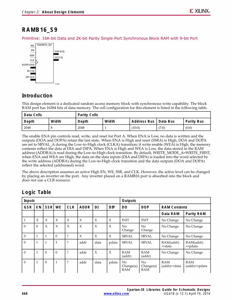
Chapter 2: About Design Elements
RAMB16_S9Primitive: 16K-bit Data and 2K-bit Parity Single-Port Synchronous Block RAM with 9-bit Port
IntroductionThis design element is a dedicated random access memory block with synchronous write capability. The blockRAM port has 16384 bits of data memory. The cell configuration for this element is listed in the following table.
Data Cells Parity CellsDepth Width Depth Width Address Bus Data Bus Parity Bus2048 8 2048 1 (10:0) (7:0) (0:0)
The enable ENA pin controls read, write, and reset for Port A. When ENA is Low, no data is written and theoutputs (DOA and DOPA) retain the last state. When ENA is High and reset (SSRA) is High, DOA and DOPAare set to SRVAL_A during the Low-to-High clock (CLKA) transition; if write enable (WEA) is High, the memorycontents reflect the data at DIA and DIPA. When ENA is High and WEA is Low, the data stored in the RAMaddress (ADDRA) is read during the Low-to-High clock transition. By default, WRITE_MODE_A=WRITE_FIRST,when ENA and WEA are High, the data on the data inputs (DIA and DIPA) is loaded into the word selected bythe write address (ADDRA) during the Low-to-High clock transition and the data outputs (DOA and DOPA)reflect the selected (addressed) word.
The above description assumes an active High EN, WE, SSR, and CLK. However, the active level can be changedby placing an inverter on the port. Any inverter placed on a RAMB16 port is absorbed into the block anddoes not use a CLB resource.
Logic TableInputs Outputs
GSR EN SSR WE CLK ADDR DI DIP DO DOP RAM ContentsData RAM Parity RAM
1 X X X X X X X INIT INIT No Change No Change
0 0 X X X X X X NoChange
NoChange
No Change No Change
0 1 1 0 ? X X X SRVAL SRVAL No Change No Change
0 1 1 1 ? addr data pdata SRVAL SRVAL RAM(addr)=>data
RAM(addr)=>pdata
0 1 0 0 ? addr X X RAM(addr)
RAM(addr)
No Change No Change
0 1 0 1 ? addr data pdata NoChange(a)RAM
NoChange(a)RAM
RAM(addr)=>data
RAM(addr)=>pdata
Spartan-3E Libraries Guide for Schematic Designs668 www.xilinx.com UG618 (v 12.1) April 19, 2010
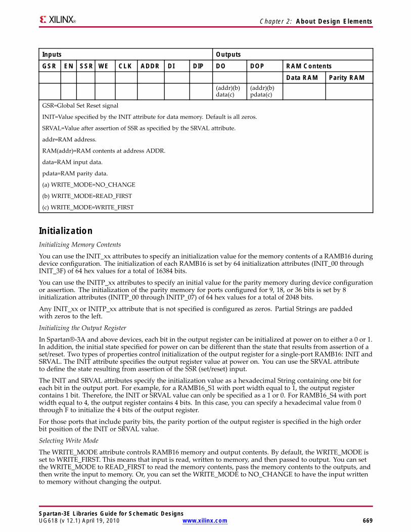
Chapter 2: About Design Elements
Inputs Outputs
GSR EN SSR WE CLK ADDR DI DIP DO DOP RAM ContentsData RAM Parity RAM
(addr)(b)data(c)
(addr)(b)pdata(c)
GSR=Global Set Reset signal
INIT=Value specified by the INIT attribute for data memory. Default is all zeros.
SRVAL=Value after assertion of SSR as specified by the SRVAL attribute.
addr=RAM address.
RAM(addr)=RAM contents at address ADDR.
data=RAM input data.
pdata=RAM parity data.
(a) WRITE_MODE=NO_CHANGE
(b) WRITE_MODE=READ_FIRST
(c) WRITE_MODE=WRITE_FIRST
InitializationInitializing Memory Contents
You can use the INIT_xx attributes to specify an initialization value for the memory contents of a RAMB16 duringdevice configuration. The initialization of each RAMB16 is set by 64 initialization attributes (INIT_00 throughINIT_3F) of 64 hex values for a total of 16384 bits.
You can use the INITP_xx attributes to specify an initial value for the parity memory during device configurationor assertion. The initialization of the parity memory for ports configured for 9, 18, or 36 bits is set by 8initialization attributes (INITP_00 through INITP_07) of 64 hex values for a total of 2048 bits.
Any INIT_xx or INITP_xx attribute that is not specified is configured as zeros. Partial Strings are paddedwith zeros to the left.
Initializing the Output Register
In Spartan®-3A and above devices, each bit in the output register can be initialized at power on to either a 0 or 1.In addition, the initial state specified for power on can be different than the state that results from assertion of aset/reset. Two types of properties control initialization of the output register for a single-port RAMB16: INIT andSRVAL. The INIT attribute specifies the output register value at power on. You can use the SRVAL attributeto define the state resulting from assertion of the SSR (set/reset) input.
The INIT and SRVAL attributes specify the initialization value as a hexadecimal String containing one bit foreach bit in the output port. For example, for a RAMB16_S1 with port width equal to 1, the output registercontains 1 bit. Therefore, the INIT or SRVAL value can only be specified as a 1 or 0. For RAMB16_S4 with portwidth equal to 4, the output register contains 4 bits. In this case, you can specify a hexadecimal value from 0through F to initialize the 4 bits of the output register.
For those ports that include parity bits, the parity portion of the output register is specified in the high orderbit position of the INIT or SRVAL value.
Selecting Write Mode
The WRITE_MODE attribute controls RAMB16 memory and output contents. By default, the WRITE_MODE isset to WRITE_FIRST. This means that input is read, written to memory, and then passed to output. You can setthe WRITE_MODE to READ_FIRST to read the memory contents, pass the memory contents to the outputs, andthen write the input to memory. Or, you can set the WRITE_MODE to NO_CHANGE to have the input writtento memory without changing the output.
Spartan-3E Libraries Guide for Schematic DesignsUG618 (v 12.1) April 19, 2010 www.xilinx.com 669

Chapter 2: About Design Elements
Design Entry MethodThis design element can be used in schematics.
Available Attributes
Attribute TypeAllowedValues Default Description
INIT Binary/Hexadecimal
Any Hex Value All zeros Identifies the initial value of theDO output port after completingconfiguration. The bit width is dependenton the width of the A or B port of theRAM.
INIT_00 toINIT_3F
Binary/Hexadecimal
Any Hex Value All zeros Specifies the initial contents of the dataportion of the RAM array.
INITP_00 toINITP_07
Binary/Hexadecimal
Any Hex Value All zeros Specifies the initial contents of the parityportion of the RAM array.
SRVAL Binary/Hexadecimal
Any Hex Value All zeros Allows the individual selection ofwhether the DO output port sets (go toa one) or reset (go to a zero) upon theassertion of the SSR pin. The bit widthis dependent on the width of the A or Bport of the RAM.
WRITE_MODE String "WRITE_FIRST","READ_FIRST"or"NO_CHANGE"
"WRITE_FIRST" Specifies the behavior of the DO portupon a write command to the respectedport. If set to "WRITE_FIRST", thesame port that is written to displaysthe contents of the written data tothe outputs upon completion of theoperation. "READ_FIRST" displaysthe prior contents of the RAM to theoutput port prior to writing the newdata. "NO_CHANGE" keeps the previousvalue on the output port and wont updatethe output port upon a write command.This is the suggested mode if not usingthe read data from a particular port of theRAM.
For More Information• See the Spartan-3 Generation FPGA User Guide.
• See the Spartan-3E FPGA Family Complete Data Sheet.
Spartan-3E Libraries Guide for Schematic Designs670 www.xilinx.com UG618 (v 12.1) April 19, 2010
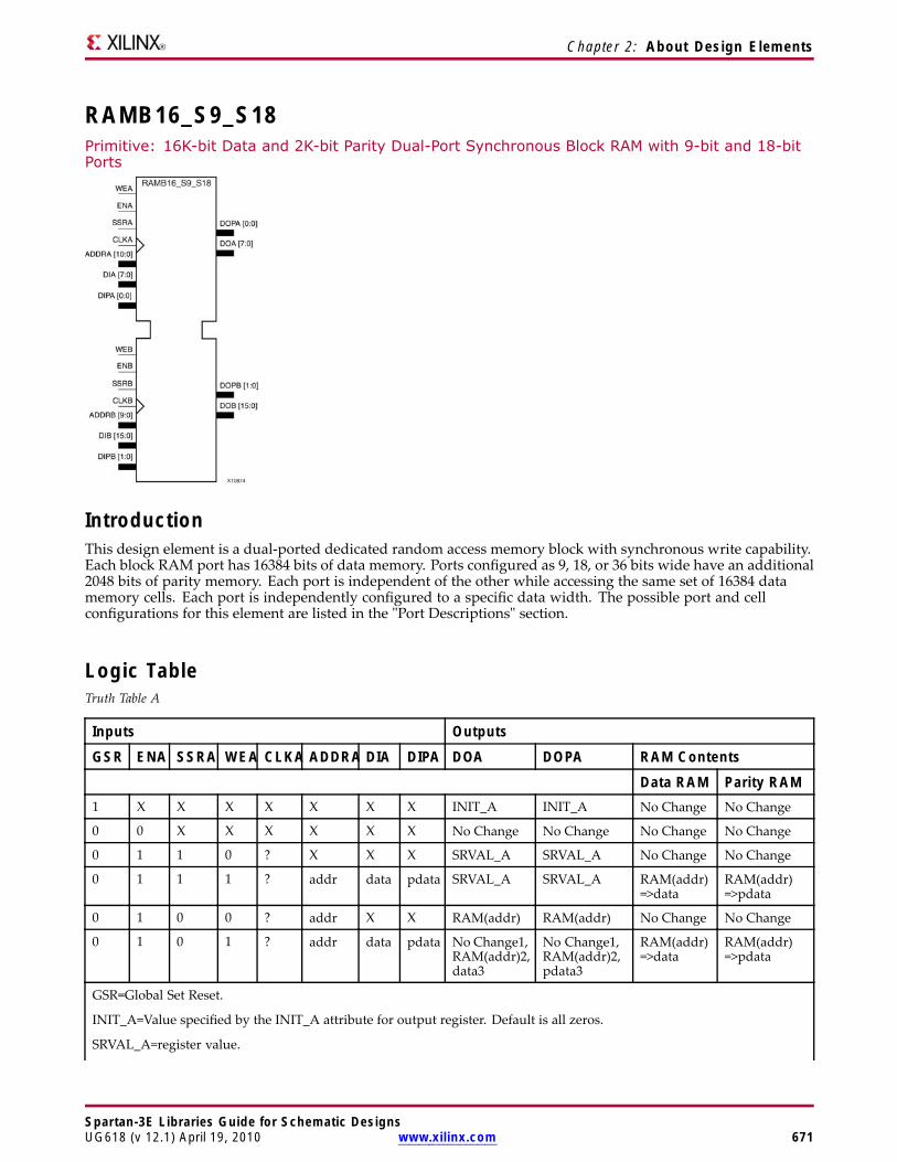
Chapter 2: About Design Elements
RAMB16_S9_S18Primitive: 16K-bit Data and 2K-bit Parity Dual-Port Synchronous Block RAM with 9-bit and 18-bitPorts
IntroductionThis design element is a dual-ported dedicated random access memory block with synchronous write capability.Each block RAM port has 16384 bits of data memory. Ports configured as 9, 18, or 36 bits wide have an additional2048 bits of parity memory. Each port is independent of the other while accessing the same set of 16384 datamemory cells. Each port is independently configured to a specific data width. The possible port and cellconfigurations for this element are listed in the "Port Descriptions" section.
Logic TableTruth Table A
Inputs Outputs
GSR ENA SSRA WEA CLKA ADDRA DIA DIPA DOA DOPA RAM ContentsData RAM Parity RAM
1 X X X X X X X INIT_A INIT_A No Change No Change
0 0 X X X X X X No Change No Change No Change No Change
0 1 1 0 ? X X X SRVAL_A SRVAL_A No Change No Change
0 1 1 1 ? addr data pdata SRVAL_A SRVAL_A RAM(addr)=>data
RAM(addr)=>pdata
0 1 0 0 ? addr X X RAM(addr) RAM(addr) No Change No Change
0 1 0 1 ? addr data pdata No Change1,RAM(addr)2,data3
No Change1,RAM(addr)2,pdata3
RAM(addr)=>data
RAM(addr)=>pdata
GSR=Global Set Reset.
INIT_A=Value specified by the INIT_A attribute for output register. Default is all zeros.
SRVAL_A=register value.
Spartan-3E Libraries Guide for Schematic DesignsUG618 (v 12.1) April 19, 2010 www.xilinx.com 671

Chapter 2: About Design Elements
Inputs Outputs
GSR ENA SSRA WEA CLKA ADDRA DIA DIPA DOA DOPA RAM ContentsData RAM Parity RAM
addr=RAM address.
RAM(addr)=RAM contents at address ADDR.
data=RAM input data.
pdata=RAM parity data.
1WRITE_MODE_A=NO_CHANGE.
2WRITE_MODE_A=READ_FIRST.
3WRITE_MODE_A=WRITE_FIRST.
Spartan-3E Libraries Guide for Schematic Designs672 www.xilinx.com UG618 (v 12.1) April 19, 2010
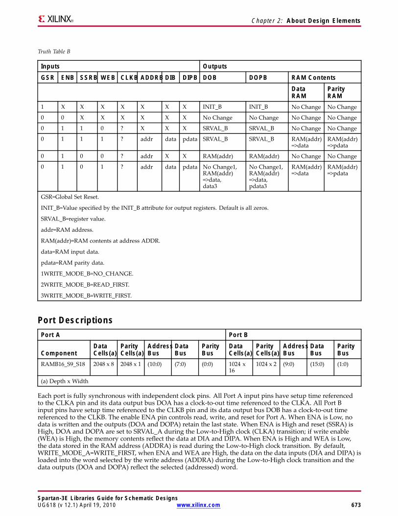
Chapter 2: About Design Elements
Truth Table B
Inputs Outputs
GSR ENB SSRB WEB CLKB ADDRB DIB DIPB DOB DOPB RAM ContentsDataRAM
ParityRAM
1 X X X X X X X INIT_B INIT_B No Change No Change
0 0 X X X X X X No Change No Change No Change No Change
0 1 1 0 ? X X X SRVAL_B SRVAL_B No Change No Change
0 1 1 1 ? addr data pdata SRVAL_B SRVAL_B RAM(addr)=>data
RAM(addr)=>pdata
0 1 0 0 ? addr X X RAM(addr) RAM(addr) No Change No Change
0 1 0 1 ? addr data pdata No Change1,RAM(addr)=>data,data3
No Change1,RAM(addr)=>data,pdata3
RAM(addr)=>data
RAM(addr)=>pdata
GSR=Global Set Reset.
INIT_B=Value specified by the INIT_B attribute for output registers. Default is all zeros.
SRVAL_B=register value.
addr=RAM address.
RAM(addr)=RAM contents at address ADDR.
data=RAM input data.
pdata=RAM parity data.
1WRITE_MODE_B=NO_CHANGE.
2WRITE_MODE_B=READ_FIRST.
3WRITE_MODE_B=WRITE_FIRST.
Port DescriptionsPort A Port B
ComponentDataCells(a)
ParityCells(a)
AddressBus
DataBus
ParityBus
DataCells(a)
ParityCells(a)
AddressBus
DataBus
ParityBus
RAMB16_S9_S18 2048 x 8 2048 x 1 (10:0) (7:0) (0:0) 1024 x16
1024 x 2 (9:0) (15:0) (1:0)
(a) Depth x Width
Each port is fully synchronous with independent clock pins. All Port A input pins have setup time referencedto the CLKA pin and its data output bus DOA has a clock-to-out time referenced to the CLKA. All Port Binput pins have setup time referenced to the CLKB pin and its data output bus DOB has a clock-to-out timereferenced to the CLKB. The enable ENA pin controls read, write, and reset for Port A. When ENA is Low, nodata is written and the outputs (DOA and DOPA) retain the last state. When ENA is High and reset (SSRA) isHigh, DOA and DOPA are set to SRVAL_A during the Low-to-High clock (CLKA) transition; if write enable(WEA) is High, the memory contents reflect the data at DIA and DIPA. When ENA is High and WEA is Low,the data stored in the RAM address (ADDRA) is read during the Low-to-High clock transition. By default,WRITE_MODE_A=WRITE_FIRST, when ENA and WEA are High, the data on the data inputs (DIA and DIPA) isloaded into the word selected by the write address (ADDRA) during the Low-to-High clock transition and thedata outputs (DOA and DOPA) reflect the selected (addressed) word.
Spartan-3E Libraries Guide for Schematic DesignsUG618 (v 12.1) April 19, 2010 www.xilinx.com 673
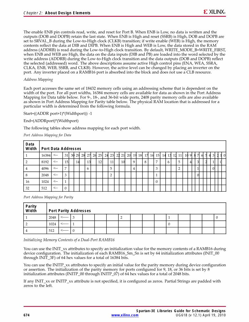
Chapter 2: About Design Elements
The enable ENB pin controls read, write, and reset for Port B. When ENB is Low, no data is written and theoutputs (DOB and DOPB) retain the last state. When ENB is High and reset (SSRB) is High, DOB and DOPB areset to SRVAL_B during the Low-to-High clock (CLKB) transition; if write enable (WEB) is High, the memorycontents reflect the data at DIB and DIPB. When ENB is High and WEB is Low, the data stored in the RAMaddress (ADDRB) is read during the Low-to-High clock transition. By default, WRITE_MODE_B=WRITE_FIRST,when ENB and WEB are High, the data on the data inputs (DIB and PB) are loaded into the word selected by thewrite address (ADDRB) during the Low-to-High clock transition and the data outputs (DOB and DOPB) reflectthe selected (addressed) word. The above descriptions assume active High control pins (ENA, WEA, SSRA,CLKA, ENB, WEB, SSRB, and CLKB). However, the active level can be changed by placing an inverter on theport. Any inverter placed on a RAMB16 port is absorbed into the block and does not use a CLB resource.
Address Mapping
Each port accesses the same set of 18432 memory cells using an addressing scheme that is dependent on thewidth of the port. For all port widths, 16384 memory cells are available for data as shown in the Port AddressMapping for Data table below. For 9-, 18-, and 36-bit wide ports, 2408 parity memory cells are also availableas shown in Port Address Mapping for Parity table below. The physical RAM location that is addressed for aparticular width is determined from the following formula.
Start=((ADDR port+1)*(Widthport)) -1
End=(ADDRport)*(Widthport)
The following tables show address mapping for each port width.
Port Address Mapping for Data
DataWidth Port Data Addresses1 16384 <-- 31 30 29 28 27 26 25 24 23 22 21 20 19 18 17 16 15 14 13 12 11 10 9 8 7 6 5 4 3 2 1 0
2 8192 <-- 15 14 13 12 11 10 9 8 7 6 5 4 3 2 1 0
4 4096 <-- 7 6 5 4 3 2 1 0
8 2048 <-- 3 2 1 0
16 1024 <-- 1 0
32 512 <-- 0
Port Address Mapping for Parity
ParityWidth Port Parity Addresses1 2048 <----- 3 2 1 0
2 1024 <----- 1 0
4 512 <----- 0
Initializing Memory Contents of a Dual-Port RAMB16
You can use the INIT_xx attributes to specify an initialization value for the memory contents of a RAMB16 duringdevice configuration. The initialization of each RAMB16_Sm_Sn is set by 64 initialization attributes (INIT_00through INIT_3F) of 64 hex values for a total of 16384 bits.
You can use the INITP_xx attributes to specify an initial value for the parity memory during device configurationor assertion. The initialization of the parity memory for ports configured for 9, 18, or 36 bits is set by 8initialization attributes (INITP_00 through INITP_07) of 64 hex values for a total of 2048 bits.
If any INIT_xx or INITP_xx attribute is not specified, it is configured as zeros. Partial Strings are padded withzeros to the left.
Spartan-3E Libraries Guide for Schematic Designs674 www.xilinx.com UG618 (v 12.1) April 19, 2010

Chapter 2: About Design Elements
Initializing the Output Register of a Dual-Port RAMB16
In Spartan®-3A and above devices, each bit in an output register can be initialized at power on (when GSR ishigh) to either a 0 or 1. In addition, the initial state specified for power on can be different than the state thatresults from assertion of a set/reset. Four properties control initialization of the output register for a dual-portRAMB16: INIT_A, INIT_B, SRVAL_A, and SRVAL_B. The INIT_A attribute specifies the output register value atpower on for Port A and the INIT_B attribute specifies the value for Port B. You can use the SRVAL_A attribute todefine the state resulting from assertion of the SSR (set/reset) input on Port A. You can use the SRVAL_B attributeto define the state resulting from assertion of the SSR input on Port B.
The INIT_A, INIT_B, SRVAL_A, and SRVAL_B attributes specify the initialization value as a hexadecimal String.The value is dependent upon the port width. For example, for a RAMB16_S1_S4 with Port A width equal to 1and Port B width equal to 4, the Port A output register contains 1 bit and the Port B output register contains 4bits. Therefore, the INIT_A or SRVAL_A value can only be specified as a 1 or 0. For Port B, the output registercontains 4 bits. In this case, you can use INIT_B or SRVAL_B to specify a hexadecimal value from 0 through F toinitialize the 4 bits of the output register.
For those ports that include parity bits, the parity portion of the output register is specified in the high order bitposition of the INIT_A, INIT_B, SRVAL_A, or SRVAL_B value.
The INIT and SRVAL attributes default to zero if they are not set by you.
Write Mode Selection
TheWRITE_MODE_A attribute controls the memory and output contents of Port A for a dual-port RAMB16. TheWRITE_MODE_B attribute does the same for Port B. By default, both WRITE_MODE_A and WRITE_MODE_Bare set to WRITE_FIRST. This means that input is read, written to memory, and then passed to output. You canset the write mode for Port A and Port B to READ_FIRST to read the memory contents, pass the memory contentsto the outputs, and then write the input to memory. Or, you can set the write mode to NO_CHANGE to havethe input written to memory without changing the output. The Port A and Port B Conflict Resolution sectiondescribes how read/write conflicts are resolved when both Port A and Port B are attempting to read/write tothe same memory cells.
Port A and Port B Conflict Resolution
Spartan-3A block SelectRAM™ is True Dual-Port RAM that allows both ports to simultaneously access the samememory cell. When one port writes to a given memory cell, the other port must not address that memory cell (fora write or a read) within the clock-to-clock setup window.
The following tables summarize the collision detection behavior of the dual-port RAMB16 based on theWRITE_MODE_A and WRITE_MODE_B settings.
WRITE_MODE_A=NO_CHANGE and WRITE_MODE_B=NO_CHANGE
WEA WEB CLKA CLKB DIA DIB DIPA DIPB DOA DOB DOPA DOPBDataRAM
ParityRam
0 0 ? ? DIA DIB DIPA DIPB RAM RAM RAM RAM NoChange
NoChange
1 0 ? ? DIA DIB DIPA DIPB NoChange
X NoChange
X DIA DIPA
0 1 ? ? DIA DIB DIPA DIPB X NoChange
X NoChange
DIB DIPB
1 1 ? ? DIA DIB DIPA DIPB NoChange
NoChange
NoChange
NoChange
X X
Spartan-3E Libraries Guide for Schematic DesignsUG618 (v 12.1) April 19, 2010 www.xilinx.com 675

Chapter 2: About Design Elements
WRITE_MODE_A=READ_FIRST and WRITE_MODE_B=READ_FIRST
WEA WEB CLKA CLKB DIA DIB DIPA DIPB DOA DOB DOPA DOPBDataRAM
ParityRam
0 0 ? ? DIA DIB DIPA DIPB RAM RAM RAM RAM NoChange
NoChange
1 0 ? ? DIA DIB DIPA DIPB RAM RAM RAM RAM DIA DIPA
0 1 ? ? DIA DIB DIPA DIPB RAM RAM RAM RAM DIB DIPB
1 1 ? ? DIA DIB DIPA DIPB RAM RAM RAM RAM X X
WRITE_MODE_A= WRITE_FIRST and WRITE_MODE_B=WRITE_FIRST
WEA WEB CLKA CLKB DIA DIB DIPA DIPB DOA DOB DOPA DOPBDataRAM
ParityRam
0 0 ? ? DIA DIB DIPA DIPB RAM RAM RAM RAM NoChange
NoChange
1 0 ? ? DIA DIB DIPA DIPB DIA X DIPA X DIA DIPA
0 1 ? ? DIA DIB DIPA DIPB X DIB X DIPB DIB DIPB
1 1 ? ? DIA DIB DIPA DIPB X X X X X X
WRITE_MODE_A=NO_CHANGE and WRITE_MODE_B=READ_FIRST
WEA WEB CLKA CLKB DIA DIB DIPA DIPB DOA DOB DOPA DOPBDataRAM
ParityRam
0 0 ? ? DIA DIB DIPA DIPB RAM RAM RAM RAM NoChange
NoChange
1 0 ? ? DIA DIB DIPA DIPB NoChange
X NoChange
X DIA DIPA
0 1 ? ? DIA DIB DIPA DIPB RAM RAM RAM RAM DIB DIPB
1 1 ? ? DIA DIB DIPA DIPB NoChange
X NoChange
X DIB DIPB
WRITE_MODE_A=NO_CHANGE and WRITE_MODE_B=WRITE_FIRST
WEA WEB CLKA CLKB DIA DIB DIPA DIPB DOA DOB DOPA DOPBDataRAM
ParityRam
0 0 ? ? DIA DIB DIPA DIPB RAM RAM RAM RAM NoChange
NoChange
1 0 ? ? DIA DIB DIPA DIPB NoChange
X NoChange
X DIA DIPA
0 1 ? ? DIA DIB DIPA DIPB X DIB X DIPB DIB DIPB
1 1 ? ? DIA DIB DIPA DIPB NoChange
X NoChange
X X X
Spartan-3E Libraries Guide for Schematic Designs676 www.xilinx.com UG618 (v 12.1) April 19, 2010

Chapter 2: About Design Elements
WRITE_MODE_A=READ_FIRST and WRITE_MODE_B=WRITE_FIRST
WEA WEB CLKA CLKB DIA DIB DIPA DIPB DOA DOB DOPA DOPBDataRAM
ParityRam
0 0 ? ? DIA DIB DIPA DIPB RAM RAM RAM RAM NoChange
NoChange
1 0 ? ? DIA DIB DIPA DIPB RAM RAM RAM RAM DIA DIPA
0 1 ? ? DIA DIB DIPA DIPB X DIB X DIPB DIB DIPB
1 1 ? ? DIA DIB DIPA DIPB X DIB X DIPB DIA DIPA
Design Entry MethodThis design element can be used in schematics.
Available Attributes
Attribute TypeAllowedValues Default Description
INIT_00 toINIT_3F
Binary/Hexadecimal
Any All zeros Specifies the initial contents of the data portionof the RAM array.
INIT_A Binary/Hexadecimal
Any All zeros Identifies the initial value of the DOA/DOB outputport after completing configuration. For Type, thebit width is dependent on the width of the A or Bport of the RAM.
INIT_B Binary/Hexadecimal
Any All zeros Identifies the initial value of the DOA/DOB outputport after completing configuration. For Type, thebit width is dependent on the width of the A or Bport of the RAM.
INITP_00 toINITP_07
Binary/Hexadecimal
Any All zeros Specifies the initial contents of the parity portionof the RAM array.
SIM_COLLISION_CHECK
String "ALL,WARNING_ONLY,"GENERATE_X_ONLY,NONE
"ALL Allows modification of the simulation behavior ifa memory collision occurs. The output is affectedas follows:
• "ALL" - Warning produced and affectedoutputs/memory location go unknown (X).
• "WARNING_ONLY" - Warning produced andaffected outputs/memory retain last value.
• "GENERATE_X_ONLY" - No warning.However, affected outputs/memory gounknown (X).
• "NONE" - No warning and affectedoutputs/memory retain last value.
Note Setting this to a value other than "ALL" canallow problems in the design go unnoticed duringsimulation. Care should be taken when changingthe value of this attribute. Please see the Synthesisand Simulation Design Guide for more information.
SRVAL_A Binary/Hexadecimal
Any All zeros Allows the individual selection of whether theDOA/DOB output port sets (go to a one) or reset(go to a zero) upon the assertion of the RSTA pin.For Type, the bit width is dependent on the widthof the A port of the RAM.
Spartan-3E Libraries Guide for Schematic DesignsUG618 (v 12.1) April 19, 2010 www.xilinx.com 677
Chapter 2: About Design Elements
Attribute TypeAllowedValues Default Description
SRVAL_B Binary/Hexadecimal
Any All zeros Allows the individual selection of whether theDOA/DOB output port sets (go to a one) or reset(go to a zero) upon the assertion of the RSTB pin.For Type, the bit width is dependent on the widthof the B port of the RAM.
WRITE_MODE_A String "WRITE_FIRST","READ_FIRST","NO_CHANGE
"WRITE_FIRST
Specifies the behavior of the DOA/DOB port upona write command to the respected port. If set to"WRITE_FIRST", the same port that is writtento displays the contents of the written data tothe outputs upon completion of the operation."READ_FIRST" displays the prior contents of theRAM to the output port prior to writing the newdata. "NO_CHANGE" keeps the previous valueon the output port and wont update the outputport upon a write command. This is the suggestedmode if not using the read data from a particularport of the RAM.
WRITE_MODE_B String "WRITE_FIRST","READ_FIRST","NO_CHANGE
"WRITE_FIRST
Specifies the behavior of the DOA/DOB port upona write command to the respected port. If set to"WRITE_FIRST", the same port that is writtento displays the contents of the written data tothe outputs upon completion of the operation."READ_FIRST" displays the prior contents of theRAM to the output port prior to writing the newdata. "NO_CHANGE" keeps the previous valueon the output port and wont update the outputport upon a write command. This is the suggestedmode if not using the read data from a particularport of the RAM.
For More Information• See the Spartan-3 Generation FPGA User Guide.
• See the Spartan-3E FPGA Family Complete Data Sheet.
Spartan-3E Libraries Guide for Schematic Designs678 www.xilinx.com UG618 (v 12.1) April 19, 2010
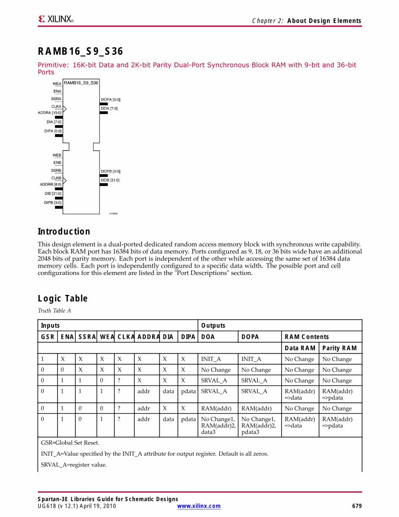
Chapter 2: About Design Elements
RAMB16_S9_S36Primitive: 16K-bit Data and 2K-bit Parity Dual-Port Synchronous Block RAM with 9-bit and 36-bitPorts
IntroductionThis design element is a dual-ported dedicated random access memory block with synchronous write capability.Each block RAM port has 16384 bits of data memory. Ports configured as 9, 18, or 36 bits wide have an additional2048 bits of parity memory. Each port is independent of the other while accessing the same set of 16384 datamemory cells. Each port is independently configured to a specific data width. The possible port and cellconfigurations for this element are listed in the "Port Descriptions" section.
Logic TableTruth Table A
Inputs Outputs
GSR ENA SSRA WEA CLKA ADDRA DIA DIPA DOA DOPA RAM ContentsData RAM Parity RAM
1 X X X X X X X INIT_A INIT_A No Change No Change
0 0 X X X X X X No Change No Change No Change No Change
0 1 1 0 ? X X X SRVAL_A SRVAL_A No Change No Change
0 1 1 1 ? addr data pdata SRVAL_A SRVAL_A RAM(addr)=>data
RAM(addr)=>pdata
0 1 0 0 ? addr X X RAM(addr) RAM(addr) No Change No Change
0 1 0 1 ? addr data pdata No Change1,RAM(addr)2,data3
No Change1,RAM(addr)2,pdata3
RAM(addr)=>data
RAM(addr)=>pdata
GSR=Global Set Reset.
INIT_A=Value specified by the INIT_A attribute for output register. Default is all zeros.
SRVAL_A=register value.
Spartan-3E Libraries Guide for Schematic DesignsUG618 (v 12.1) April 19, 2010 www.xilinx.com 679

Chapter 2: About Design Elements
Inputs Outputs
GSR ENA SSRA WEA CLKA ADDRA DIA DIPA DOA DOPA RAM ContentsData RAM Parity RAM
addr=RAM address.
RAM(addr)=RAM contents at address ADDR.
data=RAM input data.
pdata=RAM parity data.
1WRITE_MODE_A=NO_CHANGE.
2WRITE_MODE_A=READ_FIRST.
3WRITE_MODE_A=WRITE_FIRST.
Spartan-3E Libraries Guide for Schematic Designs680 www.xilinx.com UG618 (v 12.1) April 19, 2010

Chapter 2: About Design Elements
Truth Table B
Inputs Outputs
GSR ENB SSRB WEB CLKB ADDRB DIB DIPB DOB DOPB RAM ContentsDataRAM
ParityRAM
1 X X X X X X X INIT_B INIT_B No Change No Change
0 0 X X X X X X No Change No Change No Change No Change
0 1 1 0 ? X X X SRVAL_B SRVAL_B No Change No Change
0 1 1 1 ? addr data pdata SRVAL_B SRVAL_B RAM(addr)=>data
RAM(addr)=>pdata
0 1 0 0 ? addr X X RAM(addr) RAM(addr) No Change No Change
0 1 0 1 ? addr data pdata No Change1,RAM(addr)=>data,data3
No Change1,RAM(addr)=>data,pdata3
RAM(addr)=>data
RAM(addr)=>pdata
GSR=Global Set Reset.
INIT_B=Value specified by the INIT_B attribute for output registers. Default is all zeros.
SRVAL_B=register value.
addr=RAM address.
RAM(addr)=RAM contents at address ADDR.
data=RAM input data.
pdata=RAM parity data.
1WRITE_MODE_B=NO_CHANGE.
2WRITE_MODE_B=READ_FIRST.
3WRITE_MODE_B=WRITE_FIRST.
Port DescriptionsPort A Port BDesignElement
DataCells(a)
ParityCells(a)
AddressBus
DataBus
ParityBus
DataCells(a)
ParityCells(a)
AddressBus
DataBus
ParityBus
RAMB16_S9_S36 2048 x 8 2048 x 1 (10:0) (7:0) (0:0) 512 x 32 512 x 4 (8:0) (31:0) (3:0)
(a)Depth x Width
Each port is fully synchronous with independent clock pins. All Port A input pins have setup time referencedto the CLKA pin and its data output bus DOA has a clock-to-out time referenced to the CLKA. All Port Binput pins have setup time referenced to the CLKB pin and its data output bus DOB has a clock-to-out timereferenced to the CLKB. The enable ENA pin controls read, write, and reset for Port A. When ENA is Low, nodata is written and the outputs (DOA and DOPA) retain the last state. When ENA is High and reset (SSRA) isHigh, DOA and DOPA are set to SRVAL_A during the Low-to-High clock (CLKA) transition; if write enable(WEA) is High, the memory contents reflect the data at DIA and DIPA. When ENA is High and WEA is Low,the data stored in the RAM address (ADDRA) is read during the Low-to-High clock transition. By default,WRITE_MODE_A=WRITE_FIRST, when ENA and WEA are High, the data on the data inputs (DIA and DIPA) isloaded into the word selected by the write address (ADDRA) during the Low-to-High clock transition and thedata outputs (DOA and DOPA) reflect the selected (addressed) word.
Spartan-3E Libraries Guide for Schematic DesignsUG618 (v 12.1) April 19, 2010 www.xilinx.com 681

Chapter 2: About Design Elements
The enable ENB pin controls read, write, and reset for Port B. When ENB is Low, no data is written and theoutputs (DOB and DOPB) retain the last state. When ENB is High and reset (SSRB) is High, DOB and DOPB areset to SRVAL_B during the Low-to-High clock (CLKB) transition; if write enable (WEB) is High, the memorycontents reflect the data at DIB and DIPB. When ENB is High and WEB is Low, the data stored in the RAMaddress (ADDRB) is read during the Low-to-High clock transition. By default, WRITE_MODE_B=WRITE_FIRST,when ENB and WEB are High, the data on the data inputs (DIB and PB) are loaded into the word selected by thewrite address (ADDRB) during the Low-to-High clock transition and the data outputs (DOB and DOPB) reflectthe selected (addressed) word. The above descriptions assume active High control pins (ENA, WEA, SSRA,CLKA, ENB, WEB, SSRB, and CLKB). However, the active level can be changed by placing an inverter on theport. Any inverter placed on a RAMB16 port is absorbed into the block and does not use a CLB resource.
Address Mapping
Each port accesses the same set of 18432 memory cells using an addressing scheme that is dependent on thewidth of the port. For all port widths, 16384 memory cells are available for data as shown in the Port AddressMapping for Data table below. For 9-, 18-, and 36-bit wide ports, 2408 parity memory cells are also availableas shown in Port Address Mapping for Parity table below. The physical RAM location that is addressed for aparticular width is determined from the following formula.
Start=((ADDR port+1)*(Widthport)) -1
End=(ADDRport)*(Widthport)
The following tables shows address mapping for each port width.
Port Address Mapping for Data
DataWidth Port Data Addresses1 16384 <-- 31 30 29 28 27 26 25 24 23 22 21 20 19 18 17 16 15 14 13 12 11 10 9 8 7 6 5 4 3 2 1 0
2 8192 <-- 15 14 13 12 11 10 9 8 7 6 5 4 3 2 1 0
4 4096 <-- 7 6 5 4 3 2 1 0
8 2048 <-- 3 2 1 0
16 1024 <-- 1 0
32 512 <-- 0
Port Address Mapping for Parity
ParityWidth Port Parity Addresses1 2048 <----- 3 2 1 0
2 1024 <----- 1 0
4 512 <----- 0
Initializing Memory Contents of a Dual-Port RAMB16
You can use the INIT_xx attributes to specify an initialization value for the memory contents of a RAMB16 duringdevice configuration. The initialization of each RAMB16_Sm_Sn is set by 64 initialization attributes (INIT_00through INIT_3F) of 64 hex values for a total of 16384 bits.
You can use the INITP_xx attributes to specify an initial value for the parity memory during device configurationor assertion. The initialization of the parity memory for ports configured for 9, 18, or 36 bits is set by 8initialization attributes (INITP_00 through INITP_07) of 64 hex values for a total of 2048 bits.
If any INIT_xx or INITP_xx attribute is not specified, it is configured as zeros. Partial Strings are padded withzeros to the left.
Spartan-3E Libraries Guide for Schematic Designs682 www.xilinx.com UG618 (v 12.1) April 19, 2010

Chapter 2: About Design Elements
Initializing the Output Register of a Dual-Port RAMB16
In Spartan®-3A and above devices, each bit in an output register can be initialized at power on (when GSR ishigh) to either a 0 or 1. In addition, the initial state specified for power on can be different than the state thatresults from assertion of a set/reset. Four properties control initialization of the output register for a dual-portRAMB16: INIT_A, INIT_B, SRVAL_A, and SRVAL_B. The INIT_A attribute specifies the output register value atpower on for Port A and the INIT_B attribute specifies the value for Port B. You can use the SRVAL_A attribute todefine the state resulting from assertion of the SSR (set/reset) input on Port A. You can use the SRVAL_B attributeto define the state resulting from assertion of the SSR input on Port B.
The INIT_A, INIT_B, SRVAL_A, and SRVAL_B attributes specify the initialization value as a hexadecimal String.The value is dependent upon the port width. For example, for a RAMB16_S1_S4 with Port A width equal to 1and Port B width equal to 4, the Port A output register contains 1 bit and the Port B output register contains 4bits. Therefore, the INIT_A or SRVAL_A value can only be specified as a 1 or 0. For Port B, the output registercontains 4 bits. In this case, you can use INIT_B or SRVAL_B to specify a hexadecimal value from 0 through F toinitialize the 4 bits of the output register.
For those ports that include parity bits, the parity portion of the output register is specified in the high order bitposition of the INIT_A, INIT_B, SRVAL_A, or SRVAL_B value.
The INIT and SRVAL attributes default to zero if they are not set by you.
Write Mode Selection
TheWRITE_MODE_A attribute controls the memory and output contents of Port A for a dual-port RAMB16. TheWRITE_MODE_B attribute does the same for Port B. By default, both WRITE_MODE_A and WRITE_MODE_Bare set to WRITE_FIRST. This means that input is read, written to memory, and then passed to output. You canset the write mode for Port A and Port B to READ_FIRST to read the memory contents, pass the memory contentsto the outputs, and then write the input to memory. Or, you can set the write mode to NO_CHANGE to havethe input written to memory without changing the output. The Port A and Port B Conflict Resolution sectiondescribes how read/write conflicts are resolved when both Port A and Port B are attempting to read/write tothe same memory cells.
Port A and Port B Conflict Resolution
Spartan-3A block SelectRAM™ is True Dual-Port RAM that allows both ports to simultaneously access the samememory cell. When one port writes to a given memory cell, the other port must not address that memory cell (fora write or a read) within the clock-to-clock setup window.
The following tables summarize the collision detection behavior of the dual-port RAMB16 based on theWRITE_MODE_A and WRITE_MODE_B settings.
WRITE_MODE_A=NO_CHANGE and WRITE_MODE_B=NO_CHANGE
WEA WEB CLKA CLKB DIA DIB DIPA DIPB DOA DOB DOPA DOPBDataRAM
ParityRAM
0 0 ? ? DIA DIB DIPA DIPB RAM RAM RAM RAM NoChange
NoChange
1 0 ? ? DIA DIB DIPA DIPB NoChange
X NoChange
X DIA DIPA
0 1 ? ? DIA DIB DIPA DIPB X NoChange
X NoChange
DIB DIPB
1 1 ? ? DIA DIB DIPA DIPB NoChange
NoChange
NoChange
NoChange
X X
Spartan-3E Libraries Guide for Schematic DesignsUG618 (v 12.1) April 19, 2010 www.xilinx.com 683

Chapter 2: About Design Elements
WRITE_MODE_A=READ_FIRST and WRITE_MODE_B=READ_FIRST
WEA WEB CLKA CLKB DIA DIB DIPA DIPB DOA DOB DOPA DOPBDataRAM
ParityRAM
0 0 ? ? DIA DIB DIPA DIPB RAM RAM RAM RAM NoChange
NoChange
1 0 ? ? DIA DIB DIPA DIPB RAM RAM RAM RAM DIA DIPA
0 1 ? ? DIA DIB DIPA DIPB RAM RAM RAM RAM DIB DIPB
1 1 ? ? DIA DIB DIPA DIPB RAM RAM RAM RAM X X
WRITE_MODE_A= WRITE_FIRST and WRITE_MODE_B=WRITE_FIRST
WEA WEB CLKA CLKB DIA DIB DIPA DIPB DOA DOB DOPA DOPBDataRAM
ParityRAM
0 0 ? ? DIA DIB DIPA DIPB RAM RAM RAM RAM NoChange
NoChange
1 0 ? ? DIA DIB DIPA DIPB DIA X DIPA X DIA DIPA
0 1 ? ? DIA DIB DIPA DIPB X DIB X DIPB DIB DIPB
1 1 ? ? DIA DIB DIPA DIPB X X X X X X
WRITE_MODE_A=NO_CHANGE and WRITE_MODE_B=READ_FIRST
WEA WEB CLKA CLKB DIA DIB DIPA DIPB DOA DOB DOPA DOPBDataRAM
ParityRAM
0 0 ? ? DIA DIB DIPA DIPB RAM RAM RAM RAM NoChange
NoChange
1 0 ? ? DIA DIB DIPA DIPB NoChange
X NoChange
X DIA DIPA
0 1 ? ? DIA DIB DIPA DIPB RAM RAM RAM RAM DIB DIPB
1 1 ? ? DIA DIB DIPA DIPB NoChange
X NoChange
X DIB DIPB
WRITE_MODE_A=NO_CHANGE and WRITE_MODE_B=WRITE_FIRST
WEA WEB CLKA CLKB DIA DIB DIPA DIPB DOA DOB DOPA DOPBDataRAM
ParityRAM
0 0 ? ? DIA DIB DIPA DIPB RAM RAM RAM RAM NoChange
NoChange
1 0 ? ? DIA DIB DIPA DIPB NoChange
X NoChange
X DIA DIPA
0 1 ? ? DIA DIB DIPA DIPB X DIB X DIPB DIB DIPB
1 1 ? ? DIA DIB DIPA DIPB NoChange
X NoChange
X X X
Spartan-3E Libraries Guide for Schematic Designs684 www.xilinx.com UG618 (v 12.1) April 19, 2010

Chapter 2: About Design Elements
WRITE_MODE_A=READ_FIRST and WRITE_MODE_B=WRITE_FIRST
WEA WEB CLKA CLKB DIA DIB DIPA DIPB DOA DOB DOPA DOPBDataRAM
ParityRAM
0 0 ? ? DIA DIB DIPA DIPB RAM RAM RAM RAM NoChange
NoChange
1 0 ? ? DIA DIB DIPA DIPB RAM RAM RAM RAM DIA DIPA
0 1 ? ? DIA DIB DIPA DIPB X DIB X DIPB DIB DIPB
1 1 ? ? DIA DIB DIPA DIPB X DIB X DIPB DIA DIPA
Design Entry MethodThis design element can be used in schematics.
Available Attributes
Attribute TypeAllowedValues Default Description
INIT_00 toINIT_3F
Binary/Hexadecimal
Any All zeros Specifies the initial contents of the data portionof the RAM array.
INIT_A Binary/Hexadecimal
Any All zeros Identifies the initial value of the DOA/DOB outputport after completing configuration. For Type, thebit width is dependent on the width of the A or Bport of the RAM.
INIT_B Binary/Hexadecimal
Any All zeros Identifies the initial value of the DOA/DOB outputport after completing configuration. For Type, thebit width is dependent on the width of the A or Bport of the RAM.
INITP_00 toINITP_07
Binary/Hexadecimal
Any All zeros Specifies the initial contents of the parity portionof the RAM array.
SIM_COLLISION_CHECK
String "ALL,WARNING_ONLY,"GENERATE_X_ONLY,NONE
"ALL Allows modification of the simulation behavior ifa memory collision occurs. The output is affectedas follows:
• "ALL" - Warning produced and affectedoutputs/memory location go unknown (X).
• "WARNING_ONLY" - Warning produced andaffected outputs/memory retain last value.
• "GENERATE_X_ONLY" - No warning.However, affected outputs/memory gounknown (X).
• "NONE" - No warning and affectedoutputs/memory retain last value.
Note Setting this to a value other than "ALL" canallow problems in the design go unnoticed duringsimulation. Care should be taken when changingthe value of this attribute. Please see the Synthesisand Simulation Design Guide for more information.
SRVAL_A Binary/Hexadecimal
Any All zeros Allows the individual selection of whether theDOA/DOB output port sets (go to a one) or reset(go to a zero) upon the assertion of the RSTA pin.For Type, the bit width is dependent on the widthof the A port of the RAM.
Spartan-3E Libraries Guide for Schematic DesignsUG618 (v 12.1) April 19, 2010 www.xilinx.com 685

Chapter 2: About Design Elements
Attribute TypeAllowedValues Default Description
SRVAL_B Binary/Hexadecimal
Any All zeros Allows the individual selection of whether theDOA/DOB output port sets (go to a one) or reset(go to a zero) upon the assertion of the RSTB pin.For Type, the bit width is dependent on the widthof the B port of the RAM.
WRITE_MODE_A String "WRITE_FIRST","READ_FIRST","NO_CHANGE
"WRITE_FIRST
Specifies the behavior of the DOA/DOB port upona write command to the respected port. If set to"WRITE_FIRST", the same port that is writtento displays the contents of the written data tothe outputs upon completion of the operation."READ_FIRST" displays the prior contents of theRAM to the output port prior to writing the newdata. "NO_CHANGE" keeps the previous valueon the output port and wont update the outputport upon a write command. This is the suggestedmode if not using the read data from a particularport of the RAM.
WRITE_MODE_B String "WRITE_FIRST","READ_FIRST","NO_CHANGE
"WRITE_FIRST
Specifies the behavior of the DOA/DOB port upona write command to the respected port. If set to"WRITE_FIRST", the same port that is writtento displays the contents of the written data tothe outputs upon completion of the operation."READ_FIRST" displays the prior contents of theRAM to the output port prior to writing the newdata. "NO_CHANGE" keeps the previous valueon the output port and wont update the outputport upon a write command. This is the suggestedmode if not using the read data from a particularport of the RAM.
For More Information• See the Spartan-3 Generation FPGA User Guide.
• See the Spartan-3E FPGA Family Complete Data Sheet.
Spartan-3E Libraries Guide for Schematic Designs686 www.xilinx.com UG618 (v 12.1) April 19, 2010

Chapter 2: About Design Elements
RAMB16_S9_S9Primitive: 16K-bit Data and 2K-bit Parity Dual-Port Synchronous Block RAM with 9-bit Ports
IntroductionThis design element is a dual-ported dedicated random access memory block with synchronous write capability.Each block RAM port has 16384 bits of data memory. Ports configured as 9, 18, or 36 bits wide have an additional2048 bits of parity memory. Each port is independent of the other while accessing the same set of 16384 datamemory cells. Each port is independently configured to a specific data width. The possible port and cellconfigurations for this element are listed in the "Port Descriptions" section.
Logic TableTruth Table A
Inputs Outputs
GSR ENA SSRA WEA CLKA ADDRA DIA DIPA DOA DOPA RAM ContentsData RAM Parity RAM
1 X X X X X X X INIT_A INIT_A No Change No Change
0 0 X X X X X X No Change No Change No Change No Change
0 1 1 0 ? X X X SRVAL_A SRVAL_A No Change No Change
0 1 1 1 ? addr data pdata SRVAL_A SRVAL_A RAM(addr)=>data
RAM(addr)=>pdata
0 1 0 0 ? addr X X RAM(addr) RAM(addr) No Change No Change
0 1 0 1 ? addr data pdata No Change1,RAM(addr)2,data3
No Change1,RAM(addr)2,pdata3
RAM(addr)=>data
RAM(addr)=>pdata
GSR=Global Set Reset.
INIT_A=Value specified by the INIT_A attribute for output register. Default is all zeros.
SRVAL_A=register value.
Spartan-3E Libraries Guide for Schematic DesignsUG618 (v 12.1) April 19, 2010 www.xilinx.com 687
Chapter 2: About Design Elements
Inputs Outputs
GSR ENA SSRA WEA CLKA ADDRA DIA DIPA DOA DOPA RAM ContentsData RAM Parity RAM
addr=RAM address.
RAM(addr)=RAM contents at address ADDR.
data=RAM input data.
pdata=RAM parity data.
1WRITE_MODE_A=NO_CHANGE.
2WRITE_MODE_A=READ_FIRST.
3WRITE_MODE_A=WRITE_FIRST.
Spartan-3E Libraries Guide for Schematic Designs688 www.xilinx.com UG618 (v 12.1) April 19, 2010

Chapter 2: About Design Elements
Truth Table B
Inputs Outputs
GSR ENB SSRB WEB CLKB ADDRB DIB DIPB DOB DOPB RAM ContentsDataRAM
ParityRAM
1 X X X X X X X INIT_B INIT_B No Change No Change
0 0 X X X X X X No Change No Change No Change No Change
0 1 1 0 ? X X X SRVAL_B SRVAL_B No Change No Change
0 1 1 1 ? addr data pdata SRVAL_B SRVAL_B RAM(addr)=>data
RAM(addr)=>pdata
0 1 0 0 ? addr X X RAM(addr) RAM(addr) No Change No Change
0 1 0 1 ? addr data pdata No Change1,RAM(addr)=>data,data3
No Change1,RAM(addr)=>data,pdata3
RAM(addr)=>data
RAM(addr)=>pdata
GSR=Global Set Reset.
INIT_B=Value specified by the INIT_B attribute for output registers. Default is all zeros.
SRVAL_B=register value.
addr=RAM address.
RAM(addr)=RAM contents at address ADDR.
data=RAM input data.
pdata=RAM parity data.
1WRITE_MODE_B=NO_CHANGE.
2WRITE_MODE_B=READ_FIRST.
3WRITE_MODE_B=WRITE_FIRST.
Port DescriptionsPort A Port BDesignElement
DataCells(a)
ParityCells(a)
AddressBus
DataBus
ParityBus
DataCells(a)
ParityCells(a)
AddressBus
DataBus
ParityBus
RAMB16_S9_S9 2048 x 8 2048 x 1 (10:0) (7:0) (0:0) 2048 x 8 2048 x 1 (10:0) (7:0) (0:0)
(a)Depth x Width
Each port is fully synchronous with independent clock pins. All Port A input pins have setup time referencedto the CLKA pin and its data output bus DOA has a clock-to-out time referenced to the CLKA. All Port Binput pins have setup time referenced to the CLKB pin and its data output bus DOB has a clock-to-out timereferenced to the CLKB. The enable ENA pin controls read, write, and reset for Port A. When ENA is Low, nodata is written and the outputs (DOA and DOPA) retain the last state. When ENA is High and reset (SSRA) isHigh, DOA and DOPA are set to SRVAL_A during the Low-to-High clock (CLKA) transition; if write enable(WEA) is High, the memory contents reflect the data at DIA and DIPA. When ENA is High and WEA is Low,the data stored in the RAM address (ADDRA) is read during the Low-to-High clock transition. By default,WRITE_MODE_A=WRITE_FIRST, when ENA and WEA are High, the data on the data inputs (DIA and DIPA) isloaded into the word selected by the write address (ADDRA) during the Low-to-High clock transition and thedata outputs (DOA and DOPA) reflect the selected (addressed) word.
Spartan-3E Libraries Guide for Schematic DesignsUG618 (v 12.1) April 19, 2010 www.xilinx.com 689
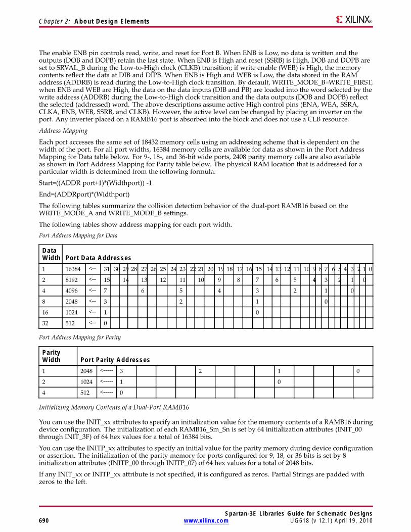
Chapter 2: About Design Elements
The enable ENB pin controls read, write, and reset for Port B. When ENB is Low, no data is written and theoutputs (DOB and DOPB) retain the last state. When ENB is High and reset (SSRB) is High, DOB and DOPB areset to SRVAL_B during the Low-to-High clock (CLKB) transition; if write enable (WEB) is High, the memorycontents reflect the data at DIB and DIPB. When ENB is High and WEB is Low, the data stored in the RAMaddress (ADDRB) is read during the Low-to-High clock transition. By default, WRITE_MODE_B=WRITE_FIRST,when ENB and WEB are High, the data on the data inputs (DIB and PB) are loaded into the word selected by thewrite address (ADDRB) during the Low-to-High clock transition and the data outputs (DOB and DOPB) reflectthe selected (addressed) word. The above descriptions assume active High control pins (ENA, WEA, SSRA,CLKA, ENB, WEB, SSRB, and CLKB). However, the active level can be changed by placing an inverter on theport. Any inverter placed on a RAMB16 port is absorbed into the block and does not use a CLB resource.
Address Mapping
Each port accesses the same set of 18432 memory cells using an addressing scheme that is dependent on thewidth of the port. For all port widths, 16384 memory cells are available for data as shown in the Port AddressMapping for Data table below. For 9-, 18-, and 36-bit wide ports, 2408 parity memory cells are also availableas shown in Port Address Mapping for Parity table below. The physical RAM location that is addressed for aparticular width is determined from the following formula.
Start=((ADDR port+1)*(Widthport)) -1
End=(ADDRport)*(Widthport)
The following tables summarize the collision detection behavior of the dual-port RAMB16 based on theWRITE_MODE_A and WRITE_MODE_B settings.
The following tables show address mapping for each port width.Port Address Mapping for Data
DataWidth Port Data Addresses1 16384 <-- 31 30 29 28 27 26 25 24 23 22 21 20 19 18 17 16 15 14 13 12 11 10 9 8 7 6 5 4 3 2 1 0
2 8192 <-- 15 14 13 12 11 10 9 8 7 6 5 4 3 2 1 0
4 4096 <-- 7 6 5 4 3 2 1 0
8 2048 <-- 3 2 1 0
16 1024 <-- 1 0
32 512 <-- 0
Port Address Mapping for Parity
ParityWidth Port Parity Addresses1 2048 <----- 3 2 1 0
2 1024 <----- 1 0
4 512 <----- 0
Initializing Memory Contents of a Dual-Port RAMB16
You can use the INIT_xx attributes to specify an initialization value for the memory contents of a RAMB16 duringdevice configuration. The initialization of each RAMB16_Sm_Sn is set by 64 initialization attributes (INIT_00through INIT_3F) of 64 hex values for a total of 16384 bits.
You can use the INITP_xx attributes to specify an initial value for the parity memory during device configurationor assertion. The initialization of the parity memory for ports configured for 9, 18, or 36 bits is set by 8initialization attributes (INITP_00 through INITP_07) of 64 hex values for a total of 2048 bits.
If any INIT_xx or INITP_xx attribute is not specified, it is configured as zeros. Partial Strings are padded withzeros to the left.
Spartan-3E Libraries Guide for Schematic Designs690 www.xilinx.com UG618 (v 12.1) April 19, 2010

Chapter 2: About Design Elements
Initializing the Output Register of a Dual-Port RAMB16
In Spartan®-3A and above devices, each bit in an output register can be initialized at power on (when GSR ishigh) to either a 0 or 1. In addition, the initial state specified for power on can be different than the state thatresults from assertion of a set/reset. Four properties control initialization of the output register for a dual-portRAMB16: INIT_A, INIT_B, SRVAL_A, and SRVAL_B. The INIT_A attribute specifies the output register value atpower on for Port A and the INIT_B attribute specifies the value for Port B. You can use the SRVAL_A attribute todefine the state resulting from assertion of the SSR (set/reset) input on Port A. You can use the SRVAL_B attributeto define the state resulting from assertion of the SSR input on Port B.
The INIT_A, INIT_B, SRVAL_A, and SRVAL_B attributes specify the initialization value as a hexadecimal String.The value is dependent upon the port width. For example, for a RAMB16_S1_S4 with Port A width equal to 1and Port B width equal to 4, the Port A output register contains 1 bit and the Port B output register contains 4bits. Therefore, the INIT_A or SRVAL_A value can only be specified as a 1 or 0. For Port B, the output registercontains 4 bits. In this case, you can use INIT_B or SRVAL_B to specify a hexadecimal value from 0 through F toinitialize the 4 bits of the output register.
For those ports that include parity bits, the parity portion of the output register is specified in the high order bitposition of the INIT_A, INIT_B, SRVAL_A, or SRVAL_B value.
The INIT and SRVAL attributes default to zero if they are not set by you.
Write Mode Selection
TheWRITE_MODE_A attribute controls the memory and output contents of Port A for a dual-port RAMB16. TheWRITE_MODE_B attribute does the same for Port B. By default, both WRITE_MODE_A and WRITE_MODE_Bare set to WRITE_FIRST. This means that input is read, written to memory, and then passed to output. You canset the write mode for Port A and Port B to READ_FIRST to read the memory contents, pass the memory contentsto the outputs, and then write the input to memory. Or, you can set the write mode to NO_CHANGE to havethe input written to memory without changing the output. The Port A and Port B Conflict Resolution sectiondescribes how read/write conflicts are resolved when both Port A and Port B are attempting to read/write tothe same memory cells.
Port A and Port B Conflict Resolution
Spartan-3A block SelectRAM™ is True Dual-Port RAM that allows both ports to simultaneously access the samememory cell. When one port writes to a given memory cell, the other port must not address that memory cell (fora write or a read) within the clock-to-clock setup window.
The following tables summarize the collision detection behavior of the dual-port RAMB16 based on theWRITE_MODE_A and WRITE_MODE_B settings.
WRITE_MODE_A=NO_CHANGE and WRITE_MODE_B=NO_CHANGE
WEA WEB CLKA CLKB DIA DIB DIPA DIPB DOA DOB DOPA DOPBDataRAM
ParityRAM
0 0 ? ? DIA DIB DIPA DIPB RAM RAM RAM RAM NoChange
NoChange
1 0 ? ? DIA DIB DIPA DIPB NoChange
X NoChange
X DIA DIPA
0 1 ? ? DIA DIB DIPA DIPB X NoChange
X NoChange
DIB DIPB
1 1 ? ? DIA DIB DIPA DIPB NoChange
NoChange
NoChange
NoChange
X X
Spartan-3E Libraries Guide for Schematic DesignsUG618 (v 12.1) April 19, 2010 www.xilinx.com 691

Chapter 2: About Design Elements
WRITE_MODE_A=READ_FIRST and WRITE_MODE_B=READ_FIRST
WEA WEB CLKA CLKB DIA DIB DIPA DIPB DOA DOB DOPA DOPBDataRAM
ParityRAM
0 0 ? ? DIA DIB DIPA DIPB RAM RAM RAM RAM NoChange
NoChange
1 0 ? ? DIA DIB DIPA DIPB RAM RAM RAM RAM DIA DIPA
0 1 ? ? DIA DIB DIPA DIPB RAM RAM RAM RAM DIB DIPB
1 1 ? ? DIA DIB DIPA DIPB RAM RAM RAM RAM X X
WRITE_MODE_A= WRITE_FIRST and WRITE_MODE_B=WRITE_FIRST
WEA WEB CLKA CLKB DIA DIB DIPA DIPB DOA DOB DOPA DOPBDataRAM
ParityRAM
0 0 ? ? DIA DIB DIPA DIPB RAM RAM RAM RAM NoChange
NoChange
1 0 ? ? DIA DIB DIPA DIPB DIA X DIPA X DIA DIPA
0 1 ? ? DIA DIB DIPA DIPB X DIB X DIPB DIB DIPB
1 1 ? ? DIA DIB DIPA DIPB X X X X X X
WRITE_MODE_A=NO_CHANGE and WRITE_MODE_B=READ_FIRST
WEA WEB CLKA CLKB DIA DIB DIPA DIPB DOA DOB DOPA DOPBDataRAM
ParityRAM
0 0 ? ? DIA DIB DIPA DIPB RAM RAM RAM RAM NoChange
NoChange
1 0 ? ? DIA DIB DIPA DIPB NoChange
X NoChange
X DIA DIPA
0 1 ? ? DIA DIB DIPA DIPB RAM RAM RAM RAM DIB DIPB
1 1 ? ? DIA DIB DIPA DIPB NoChange
X NoChange
X DIB DIPB
WRITE_MODE_A=NO_CHANGE and WRITE_MODE_B=WRITE_FIRST
WEA WEB CLKA CLKB DIA DIB DIPA DIPB DOA DOB DOPA DOPBDataRAM
ParityRAM
0 0 ? ? DIA DIB DIPA DIPB RAM RAM RAM RAM NoChange
NoChange
1 0 ? ? DIA DIB DIPA DIPB NoChange
X NoChange
X DIA DIPA
0 1 ? ? DIA DIB DIPA DIPB X DIB X DIPB DIB DIPB
1 1 ? ? DIA DIB DIPA DIPB NoChange
X NoChange
X X X
Spartan-3E Libraries Guide for Schematic Designs692 www.xilinx.com UG618 (v 12.1) April 19, 2010

Chapter 2: About Design Elements
WRITE_MODE_A=READ_FIRST and WRITE_MODE_B=WRITE_FIRST
WEA WEB CLKA CLKB DIA DIB DIPA DIPB DOA DOB DOPA DOPBDataRAM
ParityRAM
0 0 ? ? DIA DIB DIPA DIPB RAM RAM RAM RAM NoChange
NoChange
1 0 ? ? DIA DIB DIPA DIPB RAM RAM RAM RAM DIA DIPA
0 1 ? ? DIA DIB DIPA DIPB X DIB X DIPB DIB DIPB
1 1 ? ? DIA DIB DIPA DIPB X DIB X DIPB DIA DIPA
Design Entry MethodThis design element can be used in schematics.
Available Attributes
Attribute TypeAllowedValues Default Description
INIT_00 toINIT_3F
Binary/Hexadecimal
Any All zeros Specifies the initial contents of the data portionof the RAM array.
INIT_A Binary/Hexadecimal
Any All zeros Identifies the initial value of the DOA/DOB outputport after completing configuration. For Type, thebit width is dependent on the width of the A or Bport of the RAM.
INIT_B Binary/Hexadecimal
Any All zeros Identifies the initial value of the DOA/DOB outputport after completing configuration. For Type, thebit width is dependent on the width of the A or Bport of the RAM.
INITP_00 toINITP_07
Binary/Hexadecimal
Any All zeros Specifies the initial contents of the parity portionof the RAM array.
SIM_COLLISION_CHECK
String "ALL,WARNING_ONLY,"GENERATE_X_ONLY,NONE
"ALL Allows modification of the simulation behavior ifa memory collision occurs. The output is affectedas follows:
• "ALL" - Warning produced and affectedoutputs/memory location go unknown (X).
• "WARNING_ONLY" - Warning produced andaffected outputs/memory retain last value.
• "GENERATE_X_ONLY" - No warning.However, affected outputs/memory gounknown (X).
• "NONE" - No warning and affectedoutputs/memory retain last value.
Note Setting this to a value other than "ALL" canallow problems in the design go unnoticed duringsimulation. Care should be taken when changingthe value of this attribute. Please see the Synthesisand Simulation Design Guide for more information.
SRVAL_A Binary/Hexadecimal
Any All zeros Allows the individual selection of whether theDOA/DOB output port sets (go to a one) or reset(go to a zero) upon the assertion of the RSTA pin.For Type, the bit width is dependent on the widthof the A port of the RAM.
Spartan-3E Libraries Guide for Schematic DesignsUG618 (v 12.1) April 19, 2010 www.xilinx.com 693

Chapter 2: About Design Elements
Attribute TypeAllowedValues Default Description
SRVAL_B Binary/Hexadecimal
Any All zeros Allows the individual selection of whether theDOA/DOB output port sets (go to a one) or reset(go to a zero) upon the assertion of the RSTB pin.For Type, the bit width is dependent on the widthof the B port of the RAM.
WRITE_MODE_A String "WRITE_FIRST","READ_FIRST","NO_CHANGE
"WRITE_FIRST
Specifies the behavior of the DOA/DOB port upona write command to the respected port. If set to"WRITE_FIRST", the same port that is writtento displays the contents of the written data tothe outputs upon completion of the operation."READ_FIRST" displays the prior contents of theRAM to the output port prior to writing the newdata. "NO_CHANGE" keeps the previous valueon the output port and wont update the outputport upon a write command. This is the suggestedmode if not using the read data from a particularport of the RAM.
WRITE_MODE_B String "WRITE_FIRST","READ_FIRST","NO_CHANGE
"WRITE_FIRST
Specifies the behavior of the DOA/DOB port upona write command to the respected port. If set to"WRITE_FIRST", the same port that is writtento displays the contents of the written data tothe outputs upon completion of the operation."READ_FIRST" displays the prior contents of theRAM to the output port prior to writing the newdata. "NO_CHANGE" keeps the previous valueon the output port and wont update the outputport upon a write command. This is the suggestedmode if not using the read data from a particularport of the RAM.
For More Information• See the Spartan-3 Generation FPGA User Guide.
• See the Spartan-3E FPGA Family Complete Data Sheet.
Spartan-3E Libraries Guide for Schematic Designs694 www.xilinx.com UG618 (v 12.1) April 19, 2010
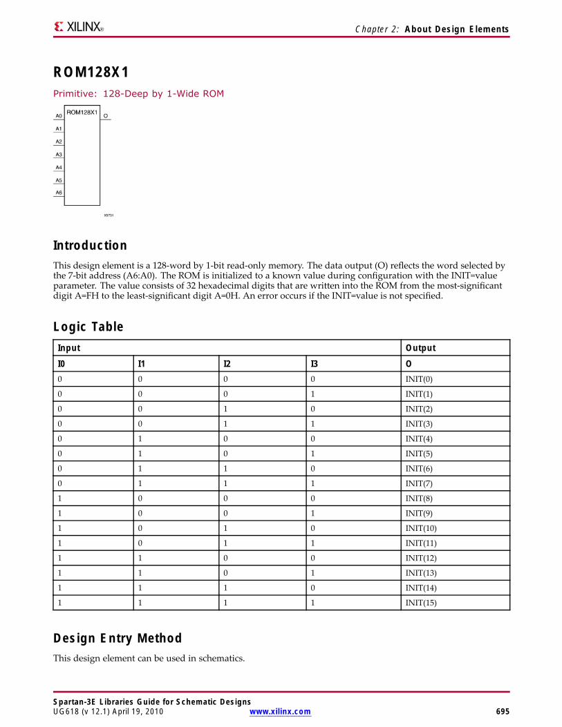
Chapter 2: About Design Elements
ROM128X1Primitive: 128-Deep by 1-Wide ROM
IntroductionThis design element is a 128-word by 1-bit read-only memory. The data output (O) reflects the word selected bythe 7-bit address (A6:A0). The ROM is initialized to a known value during configuration with the INIT=valueparameter. The value consists of 32 hexadecimal digits that are written into the ROM from the most-significantdigit A=FH to the least-significant digit A=0H. An error occurs if the INIT=value is not specified.
Logic TableInput Output
I0 I1 I2 I3 O0 0 0 0 INIT(0)
0 0 0 1 INIT(1)
0 0 1 0 INIT(2)
0 0 1 1 INIT(3)
0 1 0 0 INIT(4)
0 1 0 1 INIT(5)
0 1 1 0 INIT(6)
0 1 1 1 INIT(7)
1 0 0 0 INIT(8)
1 0 0 1 INIT(9)
1 0 1 0 INIT(10)
1 0 1 1 INIT(11)
1 1 0 0 INIT(12)
1 1 0 1 INIT(13)
1 1 1 0 INIT(14)
1 1 1 1 INIT(15)
Design Entry MethodThis design element can be used in schematics.
Spartan-3E Libraries Guide for Schematic DesignsUG618 (v 12.1) April 19, 2010 www.xilinx.com 695
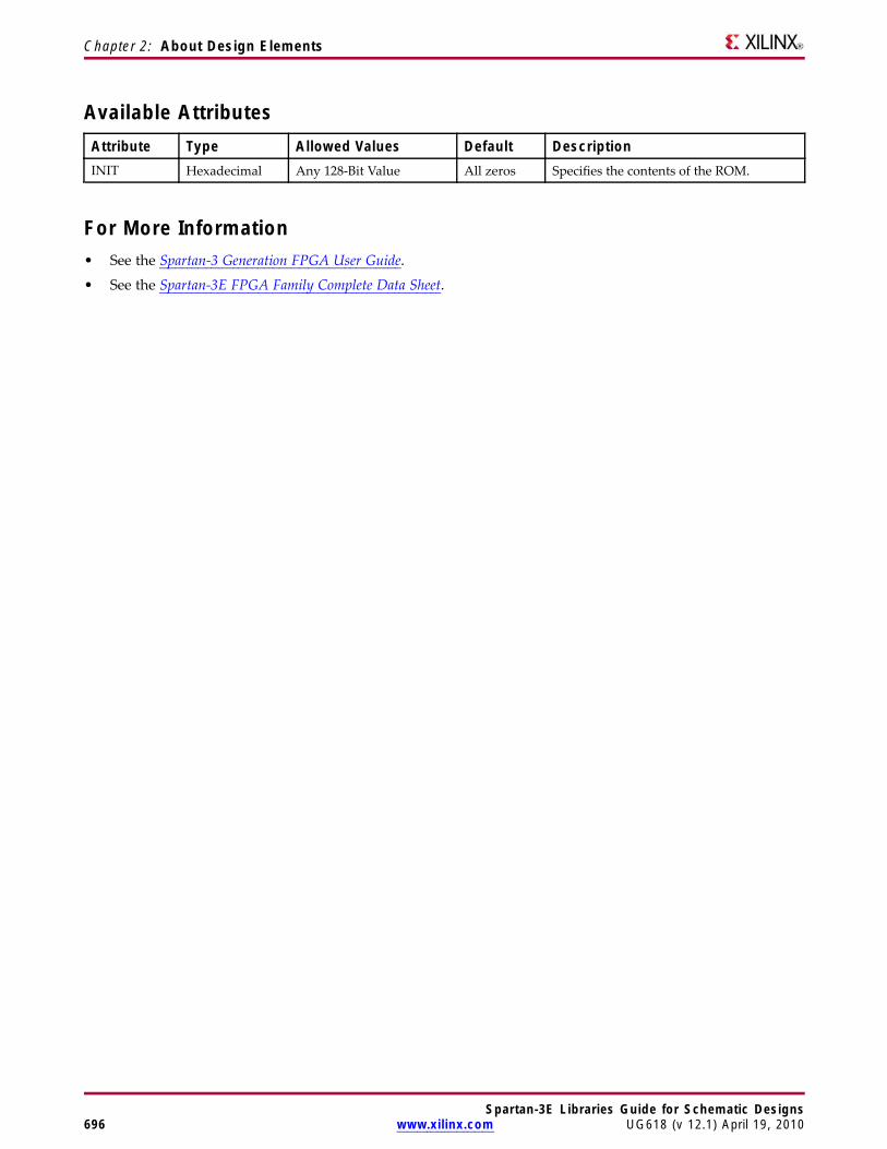
Chapter 2: About Design Elements
Available AttributesAttribute Type Allowed Values Default DescriptionINIT Hexadecimal Any 128-Bit Value All zeros Specifies the contents of the ROM.
For More Information• See the Spartan-3 Generation FPGA User Guide.
• See the Spartan-3E FPGA Family Complete Data Sheet.
Spartan-3E Libraries Guide for Schematic Designs696 www.xilinx.com UG618 (v 12.1) April 19, 2010
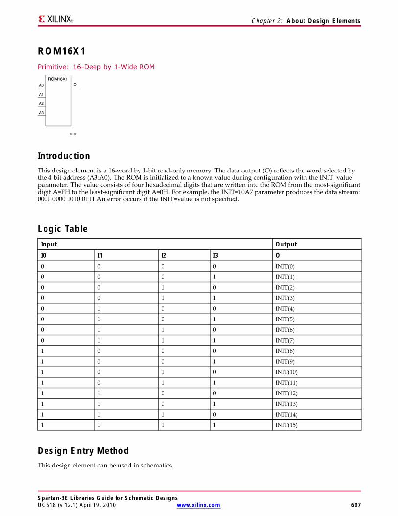
Chapter 2: About Design Elements
ROM16X1Primitive: 16-Deep by 1-Wide ROM
IntroductionThis design element is a 16-word by 1-bit read-only memory. The data output (O) reflects the word selected bythe 4-bit address (A3:A0). The ROM is initialized to a known value during configuration with the INIT=valueparameter. The value consists of four hexadecimal digits that are written into the ROM from the most-significantdigit A=FH to the least-significant digit A=0H. For example, the INIT=10A7 parameter produces the data stream:0001 0000 1010 0111 An error occurs if the INIT=value is not specified.
Logic TableInput Output
I0 I1 I2 I3 O0 0 0 0 INIT(0)
0 0 0 1 INIT(1)
0 0 1 0 INIT(2)
0 0 1 1 INIT(3)
0 1 0 0 INIT(4)
0 1 0 1 INIT(5)
0 1 1 0 INIT(6)
0 1 1 1 INIT(7)
1 0 0 0 INIT(8)
1 0 0 1 INIT(9)
1 0 1 0 INIT(10)
1 0 1 1 INIT(11)
1 1 0 0 INIT(12)
1 1 0 1 INIT(13)
1 1 1 0 INIT(14)
1 1 1 1 INIT(15)
Design Entry MethodThis design element can be used in schematics.
Spartan-3E Libraries Guide for Schematic DesignsUG618 (v 12.1) April 19, 2010 www.xilinx.com 697

Chapter 2: About Design Elements
Available AttributesAttribute Type Allowed Values Default DescriptionINIT Hexadecimal Any 16-Bit Value All zeros Specifies the contents of the ROM.
For More Information• See the Spartan-3 Generation FPGA User Guide.
• See the Spartan-3E FPGA Family Complete Data Sheet.
Spartan-3E Libraries Guide for Schematic Designs698 www.xilinx.com UG618 (v 12.1) April 19, 2010
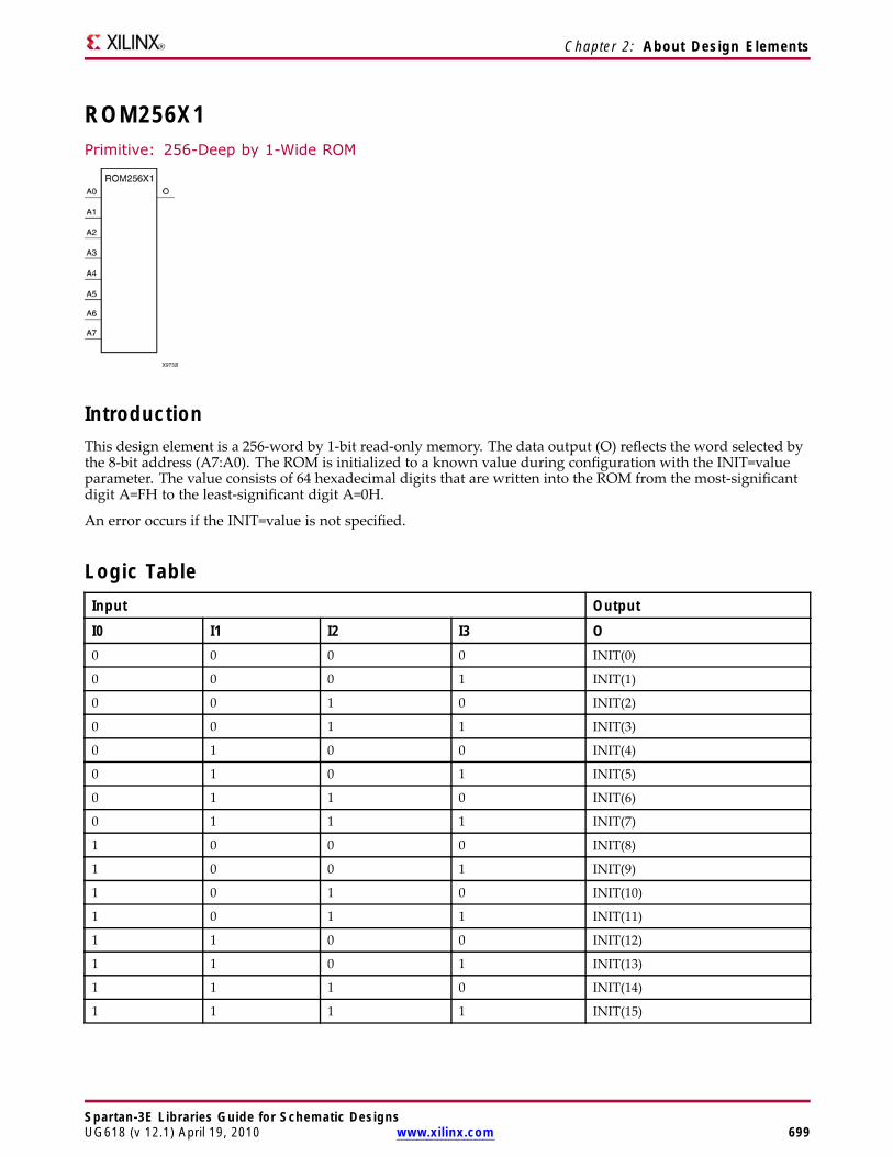
Chapter 2: About Design Elements
ROM256X1Primitive: 256-Deep by 1-Wide ROM
IntroductionThis design element is a 256-word by 1-bit read-only memory. The data output (O) reflects the word selected bythe 8-bit address (A7:A0). The ROM is initialized to a known value during configuration with the INIT=valueparameter. The value consists of 64 hexadecimal digits that are written into the ROM from the most-significantdigit A=FH to the least-significant digit A=0H.
An error occurs if the INIT=value is not specified.
Logic TableInput Output
I0 I1 I2 I3 O0 0 0 0 INIT(0)
0 0 0 1 INIT(1)
0 0 1 0 INIT(2)
0 0 1 1 INIT(3)
0 1 0 0 INIT(4)
0 1 0 1 INIT(5)
0 1 1 0 INIT(6)
0 1 1 1 INIT(7)
1 0 0 0 INIT(8)
1 0 0 1 INIT(9)
1 0 1 0 INIT(10)
1 0 1 1 INIT(11)
1 1 0 0 INIT(12)
1 1 0 1 INIT(13)
1 1 1 0 INIT(14)
1 1 1 1 INIT(15)
Spartan-3E Libraries Guide for Schematic DesignsUG618 (v 12.1) April 19, 2010 www.xilinx.com 699
Chapter 2: About Design Elements
Design Entry MethodThis design element can be used in schematics.
Available AttributesAttribute Type Allowed Values Default DescriptionINIT Hexadecimal Any 256-Bit Value All zeros Specifies the contents of the ROM.
For More Information• See the Spartan-3 Generation FPGA User Guide.
• See the Spartan-3E FPGA Family Complete Data Sheet.
Spartan-3E Libraries Guide for Schematic Designs700 www.xilinx.com UG618 (v 12.1) April 19, 2010
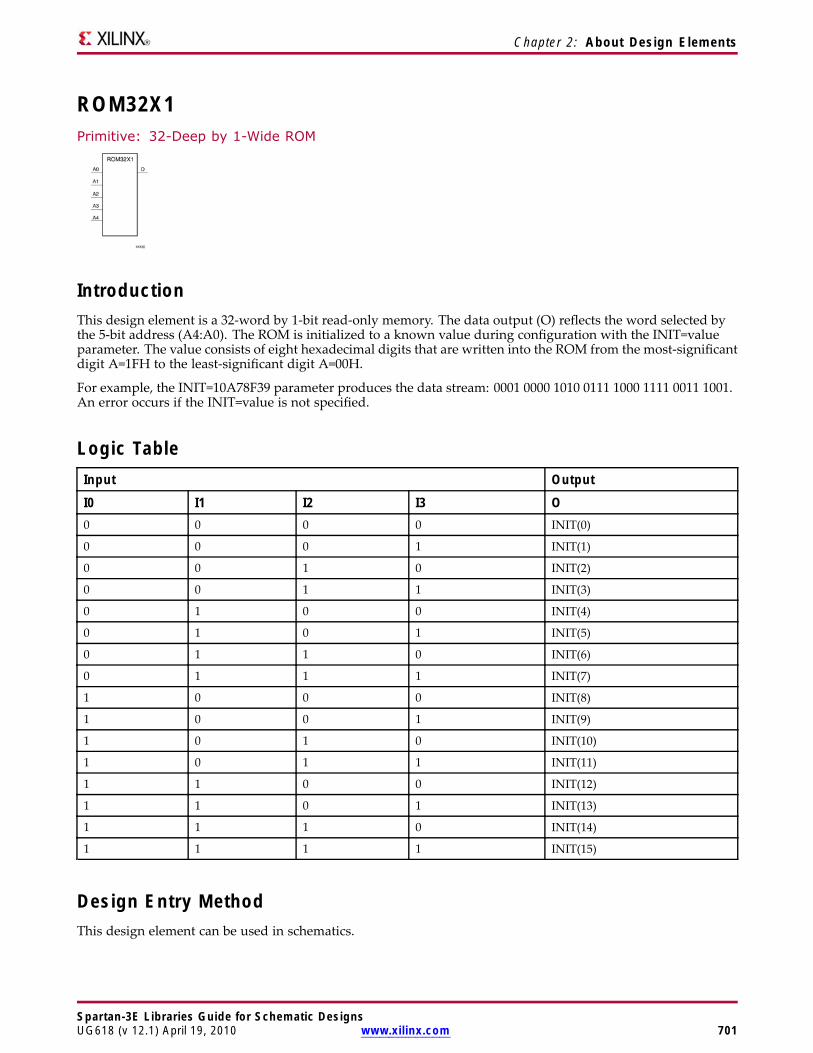
Chapter 2: About Design Elements
ROM32X1Primitive: 32-Deep by 1-Wide ROM
IntroductionThis design element is a 32-word by 1-bit read-only memory. The data output (O) reflects the word selected bythe 5-bit address (A4:A0). The ROM is initialized to a known value during configuration with the INIT=valueparameter. The value consists of eight hexadecimal digits that are written into the ROM from the most-significantdigit A=1FH to the least-significant digit A=00H.
For example, the INIT=10A78F39 parameter produces the data stream: 0001 0000 1010 0111 1000 1111 0011 1001.An error occurs if the INIT=value is not specified.
Logic TableInput Output
I0 I1 I2 I3 O0 0 0 0 INIT(0)
0 0 0 1 INIT(1)
0 0 1 0 INIT(2)
0 0 1 1 INIT(3)
0 1 0 0 INIT(4)
0 1 0 1 INIT(5)
0 1 1 0 INIT(6)
0 1 1 1 INIT(7)
1 0 0 0 INIT(8)
1 0 0 1 INIT(9)
1 0 1 0 INIT(10)
1 0 1 1 INIT(11)
1 1 0 0 INIT(12)
1 1 0 1 INIT(13)
1 1 1 0 INIT(14)
1 1 1 1 INIT(15)
Design Entry MethodThis design element can be used in schematics.
Spartan-3E Libraries Guide for Schematic DesignsUG618 (v 12.1) April 19, 2010 www.xilinx.com 701
Chapter 2: About Design Elements
Available AttributesAttribute Type Allowed Values Default DescriptionINIT Hexadecimal Any 32-Bit Value All zeros Specifies the contents of the ROM.
For More Information• See the Spartan-3 Generation FPGA User Guide.
• See the Spartan-3E FPGA Family Complete Data Sheet.
Spartan-3E Libraries Guide for Schematic Designs702 www.xilinx.com UG618 (v 12.1) April 19, 2010
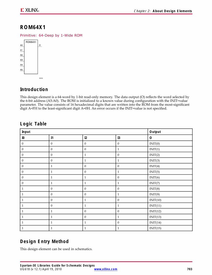
Chapter 2: About Design Elements
ROM64X1Primitive: 64-Deep by 1-Wide ROM
IntroductionThis design element is a 64-word by 1-bit read-only memory. The data output (O) reflects the word selected bythe 6-bit address (A5:A0). The ROM is initialized to a known value during configuration with the INIT=valueparameter. The value consists of 16 hexadecimal digits that are written into the ROM from the most-significantdigit A=FH to the least-significant digit A=0H. An error occurs if the INIT=value is not specified.
Logic TableInput Output
I0 I1 I2 I3 O0 0 0 0 INIT(0)
0 0 0 1 INIT(1)
0 0 1 0 INIT(2)
0 0 1 1 INIT(3)
0 1 0 0 INIT(4)
0 1 0 1 INIT(5)
0 1 1 0 INIT(6)
0 1 1 1 INIT(7)
1 0 0 0 INIT(8)
1 0 0 1 INIT(9)
1 0 1 0 INIT(10)
1 0 1 1 INIT(11)
1 1 0 0 INIT(12)
1 1 0 1 INIT(13)
1 1 1 0 INIT(14)
1 1 1 1 INIT(15)
Design Entry MethodThis design element can be used in schematics.
Spartan-3E Libraries Guide for Schematic DesignsUG618 (v 12.1) April 19, 2010 www.xilinx.com 703
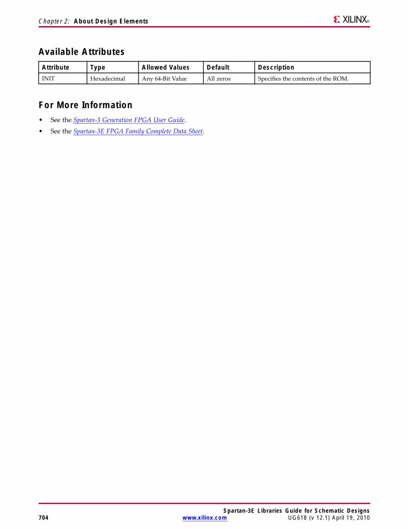
Chapter 2: About Design Elements
Available AttributesAttribute Type Allowed Values Default DescriptionINIT Hexadecimal Any 64-Bit Value All zeros Specifies the contents of the ROM.
For More Information• See the Spartan-3 Generation FPGA User Guide.
• See the Spartan-3E FPGA Family Complete Data Sheet.
Spartan-3E Libraries Guide for Schematic Designs704 www.xilinx.com UG618 (v 12.1) April 19, 2010
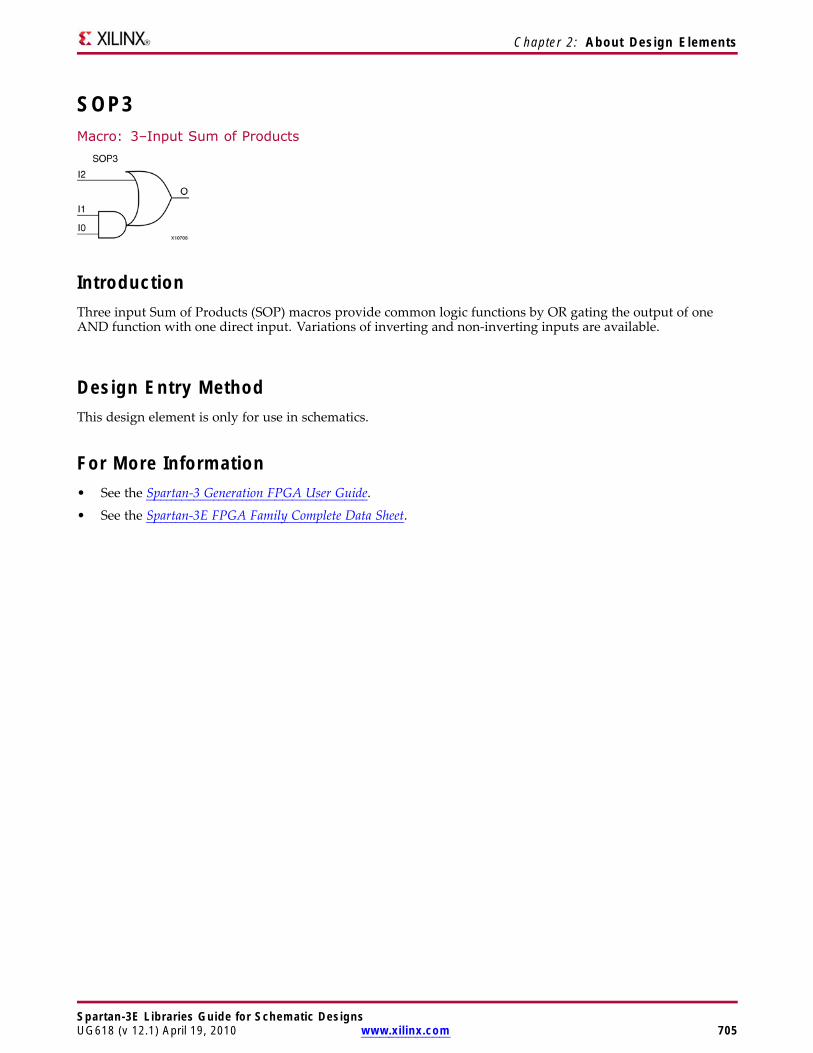
Chapter 2: About Design Elements
SOP3Macro: 3–Input Sum of Products
IntroductionThree input Sum of Products (SOP) macros provide common logic functions by OR gating the output of oneAND function with one direct input. Variations of inverting and non-inverting inputs are available.
Design Entry MethodThis design element is only for use in schematics.
For More Information• See the Spartan-3 Generation FPGA User Guide.
• See the Spartan-3E FPGA Family Complete Data Sheet.
Spartan-3E Libraries Guide for Schematic DesignsUG618 (v 12.1) April 19, 2010 www.xilinx.com 705

Chapter 2: About Design Elements
SOP3B1AMacro: 3–Input Sum of Products with One Inverted Input (Option A)
IntroductionThree input Sum of Products (SOP) macros provide common logic functions by OR gating the output of oneAND function with one direct input. Variations of inverting and non-inverting inputs are available.
Design Entry MethodThis design element is only for use in schematics.
For More Information• See the Spartan-3 Generation FPGA User Guide.
• See the Spartan-3E FPGA Family Complete Data Sheet.
Spartan-3E Libraries Guide for Schematic Designs706 www.xilinx.com UG618 (v 12.1) April 19, 2010

Chapter 2: About Design Elements
SOP3B1BMacro: 3–Input Sum of Products with One Inverted Input (Option B)
IntroductionThree input Sum of Products (SOP) macros provide common logic functions by OR gating the output of oneAND function with one direct input. Variations of inverting and non-inverting inputs are available.
Design Entry MethodThis design element is only for use in schematics.
For More Information• See the Spartan-3 Generation FPGA User Guide.
• See the Spartan-3E FPGA Family Complete Data Sheet.
Spartan-3E Libraries Guide for Schematic DesignsUG618 (v 12.1) April 19, 2010 www.xilinx.com 707

Chapter 2: About Design Elements
SOP3B2AMacro: 3–Input Sum of Products with Two Inverted Inputs (Option A)
IntroductionThree input Sum of Products (SOP) macros provide common logic functions by OR gating the output of oneAND function with one direct input. Variations of inverting and non-inverting inputs are available.
Design Entry MethodThis design element is only for use in schematics.
For More Information• See the Spartan-3 Generation FPGA User Guide.
• See the Spartan-3E FPGA Family Complete Data Sheet.
Spartan-3E Libraries Guide for Schematic Designs708 www.xilinx.com UG618 (v 12.1) April 19, 2010
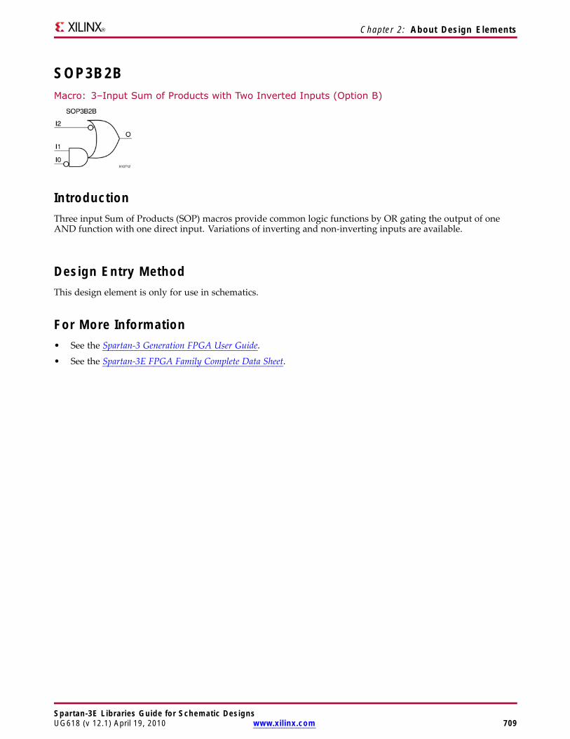
Chapter 2: About Design Elements
SOP3B2BMacro: 3–Input Sum of Products with Two Inverted Inputs (Option B)
IntroductionThree input Sum of Products (SOP) macros provide common logic functions by OR gating the output of oneAND function with one direct input. Variations of inverting and non-inverting inputs are available.
Design Entry MethodThis design element is only for use in schematics.
For More Information• See the Spartan-3 Generation FPGA User Guide.
• See the Spartan-3E FPGA Family Complete Data Sheet.
Spartan-3E Libraries Guide for Schematic DesignsUG618 (v 12.1) April 19, 2010 www.xilinx.com 709

Chapter 2: About Design Elements
SOP3B3Macro: 3–Input Sum of Products with Inverted Inputs
IntroductionThree input Sum of Products (SOP) macros provide common logic functions by OR gating the output of oneAND function with one direct input. Variations of inverting and non-inverting inputs are available.
Design Entry MethodThis design element is only for use in schematics.
For More Information• See the Spartan-3 Generation FPGA User Guide.
• See the Spartan-3E FPGA Family Complete Data Sheet.
Spartan-3E Libraries Guide for Schematic Designs710 www.xilinx.com UG618 (v 12.1) April 19, 2010
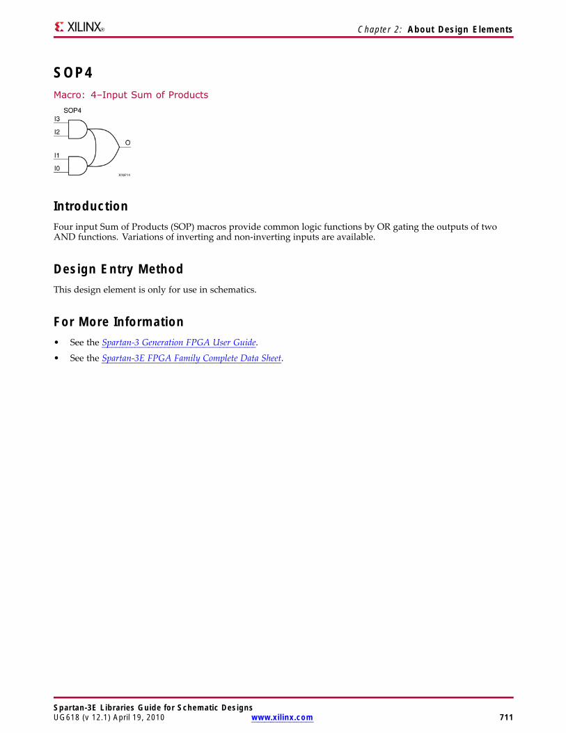
Chapter 2: About Design Elements
SOP4Macro: 4–Input Sum of Products
IntroductionFour input Sum of Products (SOP) macros provide common logic functions by OR gating the outputs of twoAND functions. Variations of inverting and non-inverting inputs are available.
Design Entry MethodThis design element is only for use in schematics.
For More Information• See the Spartan-3 Generation FPGA User Guide.
• See the Spartan-3E FPGA Family Complete Data Sheet.
Spartan-3E Libraries Guide for Schematic DesignsUG618 (v 12.1) April 19, 2010 www.xilinx.com 711
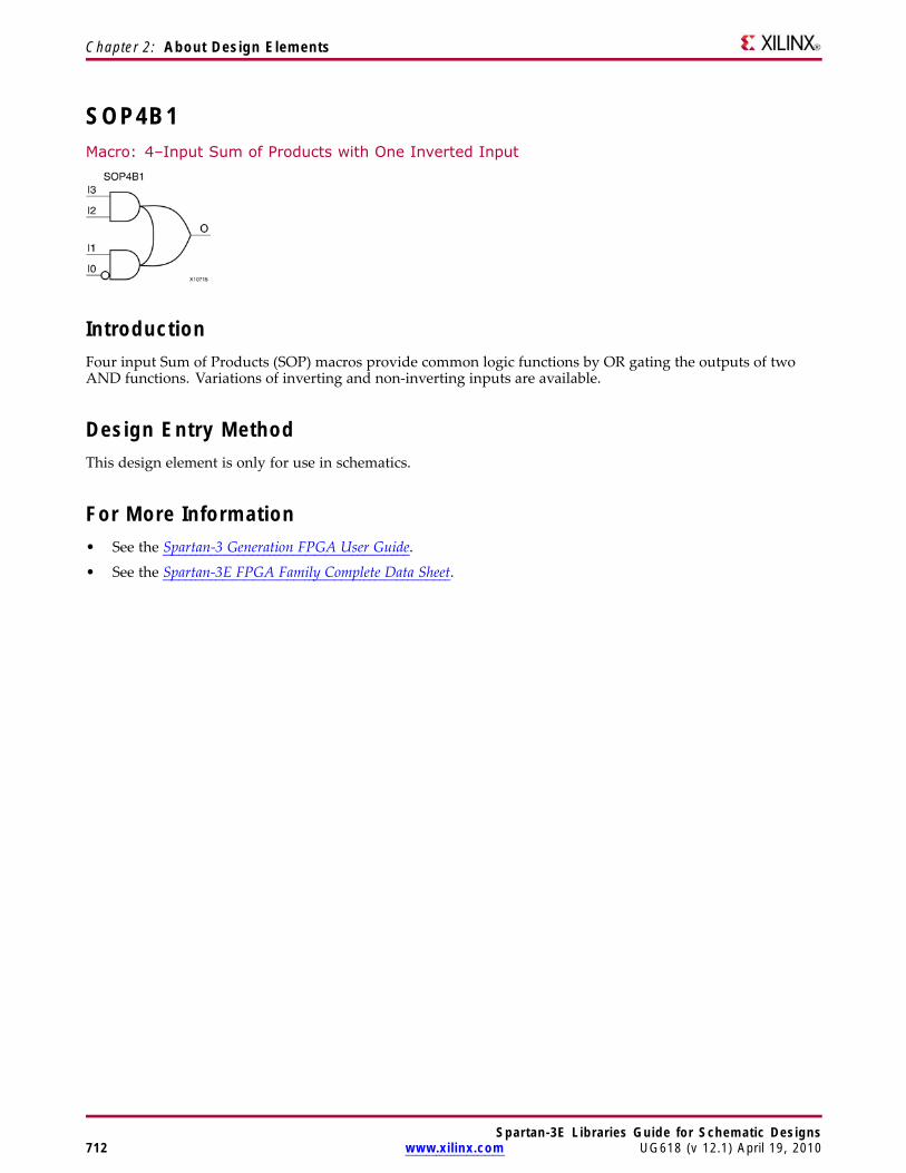
Chapter 2: About Design Elements
SOP4B1Macro: 4–Input Sum of Products with One Inverted Input
IntroductionFour input Sum of Products (SOP) macros provide common logic functions by OR gating the outputs of twoAND functions. Variations of inverting and non-inverting inputs are available.
Design Entry MethodThis design element is only for use in schematics.
For More Information• See the Spartan-3 Generation FPGA User Guide.
• See the Spartan-3E FPGA Family Complete Data Sheet.
Spartan-3E Libraries Guide for Schematic Designs712 www.xilinx.com UG618 (v 12.1) April 19, 2010
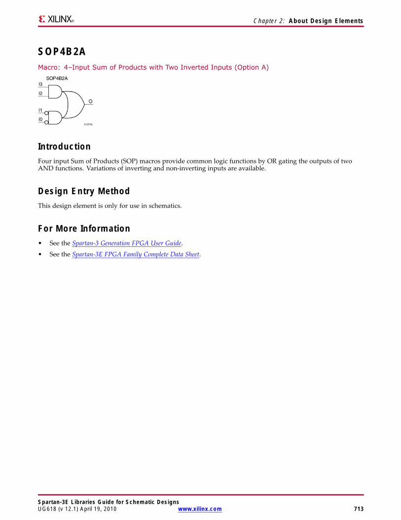
Chapter 2: About Design Elements
SOP4B2AMacro: 4–Input Sum of Products with Two Inverted Inputs (Option A)
IntroductionFour input Sum of Products (SOP) macros provide common logic functions by OR gating the outputs of twoAND functions. Variations of inverting and non-inverting inputs are available.
Design Entry MethodThis design element is only for use in schematics.
For More Information• See the Spartan-3 Generation FPGA User Guide.
• See the Spartan-3E FPGA Family Complete Data Sheet.
Spartan-3E Libraries Guide for Schematic DesignsUG618 (v 12.1) April 19, 2010 www.xilinx.com 713
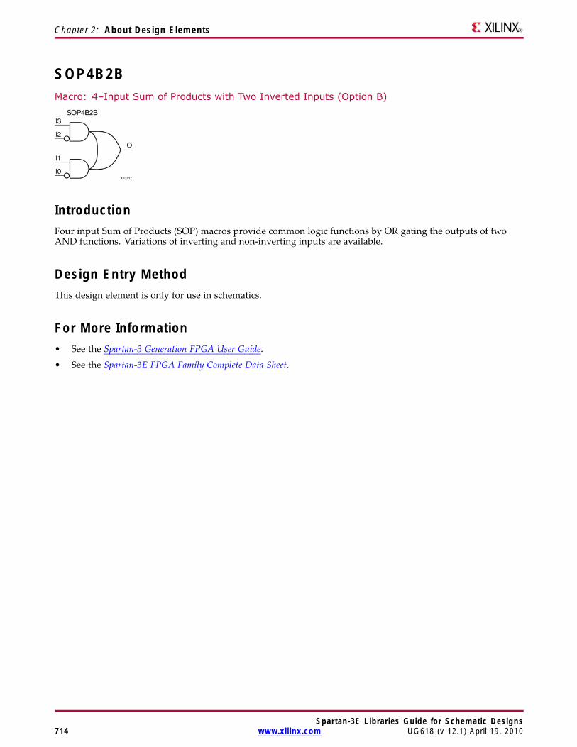
Chapter 2: About Design Elements
SOP4B2BMacro: 4–Input Sum of Products with Two Inverted Inputs (Option B)
IntroductionFour input Sum of Products (SOP) macros provide common logic functions by OR gating the outputs of twoAND functions. Variations of inverting and non-inverting inputs are available.
Design Entry MethodThis design element is only for use in schematics.
For More Information• See the Spartan-3 Generation FPGA User Guide.
• See the Spartan-3E FPGA Family Complete Data Sheet.
Spartan-3E Libraries Guide for Schematic Designs714 www.xilinx.com UG618 (v 12.1) April 19, 2010
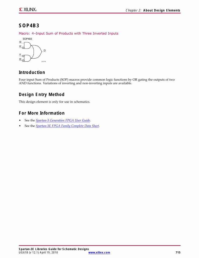
Chapter 2: About Design Elements
SOP4B3Macro: 4–Input Sum of Products with Three Inverted Inputs
IntroductionFour input Sum of Products (SOP) macros provide common logic functions by OR gating the outputs of twoAND functions. Variations of inverting and non-inverting inputs are available.
Design Entry MethodThis design element is only for use in schematics.
For More Information• See the Spartan-3 Generation FPGA User Guide.
• See the Spartan-3E FPGA Family Complete Data Sheet.
Spartan-3E Libraries Guide for Schematic DesignsUG618 (v 12.1) April 19, 2010 www.xilinx.com 715
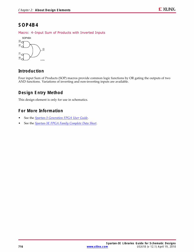
Chapter 2: About Design Elements
SOP4B4Macro: 4–Input Sum of Products with Inverted Inputs
IntroductionFour input Sum of Products (SOP) macros provide common logic functions by OR gating the outputs of twoAND functions. Variations of inverting and non-inverting inputs are available.
Design Entry MethodThis design element is only for use in schematics.
For More Information• See the Spartan-3 Generation FPGA User Guide.
• See the Spartan-3E FPGA Family Complete Data Sheet.
Spartan-3E Libraries Guide for Schematic Designs716 www.xilinx.com UG618 (v 12.1) April 19, 2010

Chapter 2: About Design Elements
SR16CEMacro: 16-Bit Serial-In Parallel-Out Shift Register with Clock Enable and Asynchronous Clear
IntroductionThis design element is a shift register with a shift-left serial input (SLI), parallel outputs (Q), and clock enable(CE) and asynchronous clear (CLR) inputs. The (CLR) input, when High, overrides all other inputs and resets thedata outputs (Q) Low. When (CE) is High and (CLR) is Low, the data on the SLI input is loaded into the firstbit of the shift register during the Low-to- High clock (C) transition and appears on the (Q0) output. Duringsubsequent Low-to- High clock transitions, when (CE) is High and (CLR) is Low, data shifts to the next highestbit position as new data is loaded into (Q0) (SLI→Q0, Q0→Q1, Q1→Q2, and so forth). The register ignores clocktransitions when (CE) is Low.
Registers can be cascaded by connecting the last (Q) output of one stage to the SLI input of the next stageand connecting clock, (CE), and (CLR) in parallel.
This register is asynchronously cleared, outputs Low, when power is applied. For FPGA devices, power-onconditions are simulated when global set/reset (GSR) is active. GSR defaults to active-High but can be invertedby adding an inverter in front of the GSR input of the appropriate STARTUP_architecture symbol.
Logic TableInputs Outputs
CLR CE SLI C Q0 Qz : Q11 X X X 0 0
0 0 X X No Change No Change
0 1 SLI ↑ SLI qn-1
z = bit width - 1
qn-1 = state of referenced output one setup time prior to active clock transition
Design Entry MethodThis design element is only for use in schematics.
For More Information• See the Spartan-3 Generation FPGA User Guide.
• See the Spartan-3E FPGA Family Complete Data Sheet.
Spartan-3E Libraries Guide for Schematic DesignsUG618 (v 12.1) April 19, 2010 www.xilinx.com 717
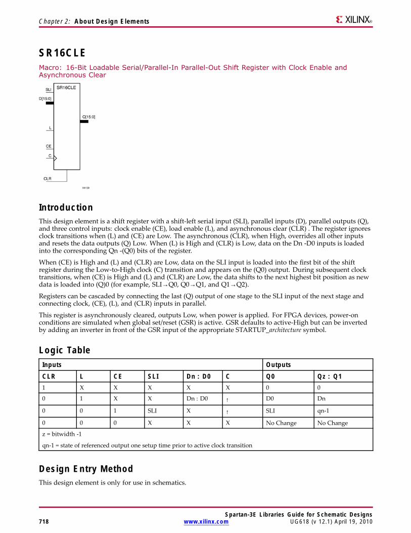
Chapter 2: About Design Elements
SR16CLEMacro: 16-Bit Loadable Serial/Parallel-In Parallel-Out Shift Register with Clock Enable andAsynchronous Clear
IntroductionThis design element is a shift register with a shift-left serial input (SLI), parallel inputs (D), parallel outputs (Q),and three control inputs: clock enable (CE), load enable (L), and asynchronous clear (CLR) . The register ignoresclock transitions when (L) and (CE) are Low. The asynchronous (CLR), when High, overrides all other inputsand resets the data outputs (Q) Low. When (L) is High and (CLR) is Low, data on the Dn -D0 inputs is loadedinto the corresponding Qn -(Q0) bits of the register.
When (CE) is High and (L) and (CLR) are Low, data on the SLI input is loaded into the first bit of the shiftregister during the Low-to-High clock (C) transition and appears on the (Q0) output. During subsequent clocktransitions, when (CE) is High and (L) and (CLR) are Low, the data shifts to the next highest bit position as newdata is loaded into (Q)0 (for example, SLI→Q0, Q0→Q1, and Q1→Q2).
Registers can be cascaded by connecting the last (Q) output of one stage to the SLI input of the next stage andconnecting clock, (CE), (L), and (CLR) inputs in parallel.
This register is asynchronously cleared, outputs Low, when power is applied. For FPGA devices, power-onconditions are simulated when global set/reset (GSR) is active. GSR defaults to active-High but can be invertedby adding an inverter in front of the GSR input of the appropriate STARTUP_architecture symbol.
Logic TableInputs Outputs
CLR L CE SLI Dn : D0 C Q0 Qz : Q11 X X X X X 0 0
0 1 X X Dn : D0 ↑ D0 Dn
0 0 1 SLI X ↑ SLI qn-1
0 0 0 X X X No Change No Change
z = bitwidth -1
qn-1 = state of referenced output one setup time prior to active clock transition
Design Entry MethodThis design element is only for use in schematics.
Spartan-3E Libraries Guide for Schematic Designs718 www.xilinx.com UG618 (v 12.1) April 19, 2010

Chapter 2: About Design Elements
For More Information• See the Spartan-3 Generation FPGA User Guide.
• See the Spartan-3E FPGA Family Complete Data Sheet.
Spartan-3E Libraries Guide for Schematic DesignsUG618 (v 12.1) April 19, 2010 www.xilinx.com 719
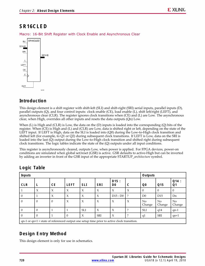
Chapter 2: About Design Elements
SR16CLEDMacro: 16-Bit Shift Register with Clock Enable and Asynchronous Clear
IntroductionThis design element is a shift register with shift-left (SLI) and shift-right (SRI) serial inputs, parallel inputs (D),parallel outputs (Q), and four control inputs: clock enable (CE), load enable (L), shift left/right (LEFT), andasynchronous clear (CLR). The register ignores clock transitions when (CE) and (L) are Low. The asynchronousclear, when High, overrides all other inputs and resets the data outputs (Qn) Low.
When (L) is High and (CLR) is Low, the data on the (D) inputs is loaded into the corresponding (Q) bits of theregister. When (CE) is High and (L) and (CLR) are Low, data is shifted right or left, depending on the state of theLEFT input. If LEFT is High, data on the SLI is loaded into (Q0) during the Low-to-High clock transition andshifted left (for example, to Q1 or Q2) during subsequent clock transitions. If LEFT is Low, data on the SRI isloaded into the last (Q) output during the Low-to-High clock transition and shifted right during subsequentclock transitions. The logic tables indicate the state of the (Q) outputs under all input conditions.
This register is asynchronously cleared, outputs Low, when power is applied. For FPGA devices, power-onconditions are simulated when global set/reset (GSR) is active. GSR defaults to active-High but can be invertedby adding an inverter in front of the GSR input of the appropriate STARTUP_architecture symbol.
Logic TableInputs Outputs
CLR L CE LEFT SLI SRID15 :D0 C Q0 Q15
Q14 :Q1
1 X X X X X X X 0 0 0
0 1 X X X X D15 : D0 ? D0 D15 Dn
0 0 0 X X X X X NoChange
NoChange
NoChange
0 0 1 1 SLI X X ? SLI q14 qn-1
0 0 1 0 X SRI X ? q1 SRI qn+1
qn-1 or qn+1 = state of referenced output one setup time prior to active clock transition.
Design Entry MethodThis design element is only for use in schematics.
Spartan-3E Libraries Guide for Schematic Designs720 www.xilinx.com UG618 (v 12.1) April 19, 2010

Chapter 2: About Design Elements
For More Information• See the Spartan-3 Generation FPGA User Guide.
• See the Spartan-3E FPGA Family Complete Data Sheet.
Spartan-3E Libraries Guide for Schematic DesignsUG618 (v 12.1) April 19, 2010 www.xilinx.com 721

Chapter 2: About Design Elements
SR16REMacro: 16-Bit Serial-In Parallel-Out Shift Register with Clock Enable and Synchronous Reset
IntroductionThis design element is a shift register with shift-left serial input (SLI), parallel outputs (Qn), clock enable (CE),and synchronous reset (R) inputs. The R input, when High, overrides all other inputs during the Low-to-Highclock (C) transition and resets the data outputs (Q) Low.
When (CE) is High and (R) is Low, the data on the (SLI) is loaded into the first bit of the shift register duringthe Low-to-High clock (C) transition and appears on the (Q0) output. During subsequent Low-to-High clocktransitions, when (CE) is High and R is Low, data shifts to the next highest bit position as new data is loaded into(Q0) (for example, SLI→Q0, Q0→Q1, and Q1→Q2). The register ignores clock transitions when (CE) is Low.
Registers can be cascaded by connecting the last (Q) output of one stage to the SLI input of the next stage andconnecting clock, (CE), and (R) in parallel.
This register is asynchronously cleared, outputs Low, when power is applied. For FPGA devices, power-onconditions are simulated when global set/reset (GSR) is active. GSR defaults to active-High but can be invertedby adding an inverter in front of the GSR input of the appropriate STARTUP_architecture symbol.
Logic TableInputs Outputs
R CE SLI C Q0 Qz : Q11 X X ↑ 0 0
0 0 X X No Change No Change
0 1 SLI ↑ SLI qn-1
z = bitwidth -1
qn-1 = state of referenced output one setup time prior to active clock transition
Design Entry MethodThis design element is only for use in schematics.
For More Information• See the Spartan-3 Generation FPGA User Guide.
• See the Spartan-3E FPGA Family Complete Data Sheet.
Spartan-3E Libraries Guide for Schematic Designs722 www.xilinx.com UG618 (v 12.1) April 19, 2010
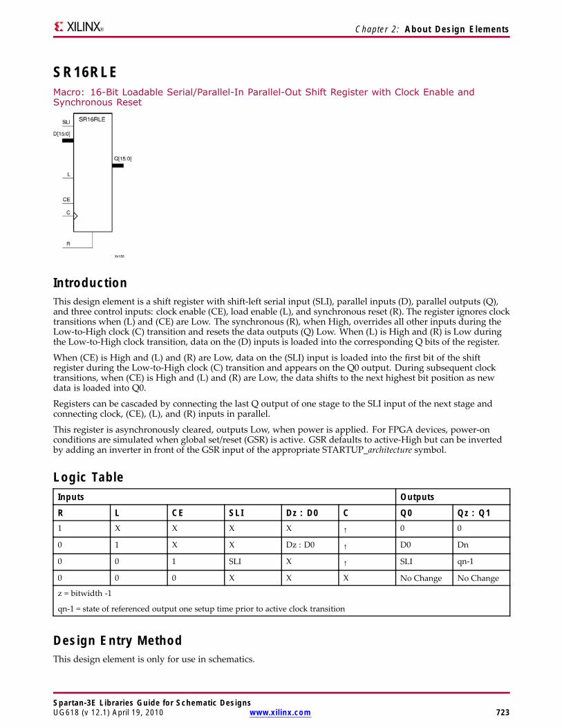
Chapter 2: About Design Elements
SR16RLEMacro: 16-Bit Loadable Serial/Parallel-In Parallel-Out Shift Register with Clock Enable andSynchronous Reset
IntroductionThis design element is a shift register with shift-left serial input (SLI), parallel inputs (D), parallel outputs (Q),and three control inputs: clock enable (CE), load enable (L), and synchronous reset (R). The register ignores clocktransitions when (L) and (CE) are Low. The synchronous (R), when High, overrides all other inputs during theLow-to-High clock (C) transition and resets the data outputs (Q) Low. When (L) is High and (R) is Low duringthe Low-to-High clock transition, data on the (D) inputs is loaded into the corresponding Q bits of the register.
When (CE) is High and (L) and (R) are Low, data on the (SLI) input is loaded into the first bit of the shiftregister during the Low-to-High clock (C) transition and appears on the Q0 output. During subsequent clocktransitions, when (CE) is High and (L) and (R) are Low, the data shifts to the next highest bit position as newdata is loaded into Q0.
Registers can be cascaded by connecting the last Q output of one stage to the SLI input of the next stage andconnecting clock, (CE), (L), and (R) inputs in parallel.
This register is asynchronously cleared, outputs Low, when power is applied. For FPGA devices, power-onconditions are simulated when global set/reset (GSR) is active. GSR defaults to active-High but can be invertedby adding an inverter in front of the GSR input of the appropriate STARTUP_architecture symbol.
Logic TableInputs Outputs
R L CE SLI Dz : D0 C Q0 Qz : Q11 X X X X ↑ 0 0
0 1 X X Dz : D0 ↑ D0 Dn
0 0 1 SLI X ↑ SLI qn-1
0 0 0 X X X No Change No Change
z = bitwidth -1
qn-1 = state of referenced output one setup time prior to active clock transition
Design Entry MethodThis design element is only for use in schematics.
Spartan-3E Libraries Guide for Schematic DesignsUG618 (v 12.1) April 19, 2010 www.xilinx.com 723

Chapter 2: About Design Elements
For More Information• See the Spartan-3 Generation FPGA User Guide.
• See the Spartan-3E FPGA Family Complete Data Sheet.
Spartan-3E Libraries Guide for Schematic Designs724 www.xilinx.com UG618 (v 12.1) April 19, 2010
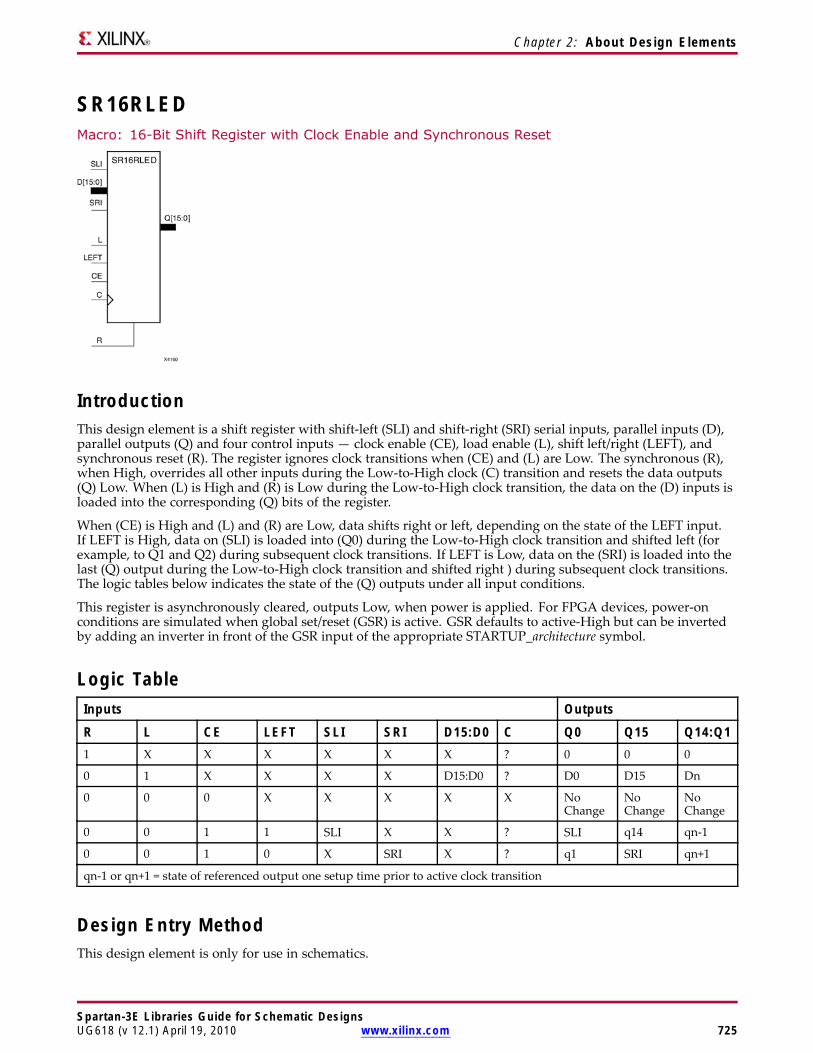
Chapter 2: About Design Elements
SR16RLEDMacro: 16-Bit Shift Register with Clock Enable and Synchronous Reset
IntroductionThis design element is a shift register with shift-left (SLI) and shift-right (SRI) serial inputs, parallel inputs (D),parallel outputs (Q) and four control inputs — clock enable (CE), load enable (L), shift left/right (LEFT), andsynchronous reset (R). The register ignores clock transitions when (CE) and (L) are Low. The synchronous (R),when High, overrides all other inputs during the Low-to-High clock (C) transition and resets the data outputs(Q) Low. When (L) is High and (R) is Low during the Low-to-High clock transition, the data on the (D) inputs isloaded into the corresponding (Q) bits of the register.
When (CE) is High and (L) and (R) are Low, data shifts right or left, depending on the state of the LEFT input.If LEFT is High, data on (SLI) is loaded into (Q0) during the Low-to-High clock transition and shifted left (forexample, to Q1 and Q2) during subsequent clock transitions. If LEFT is Low, data on the (SRI) is loaded into thelast (Q) output during the Low-to-High clock transition and shifted right ) during subsequent clock transitions.The logic tables below indicates the state of the (Q) outputs under all input conditions.
This register is asynchronously cleared, outputs Low, when power is applied. For FPGA devices, power-onconditions are simulated when global set/reset (GSR) is active. GSR defaults to active-High but can be invertedby adding an inverter in front of the GSR input of the appropriate STARTUP_architecture symbol.
Logic TableInputs Outputs
R L CE LEFT SLI SRI D15:D0 C Q0 Q15 Q14:Q11 X X X X X X ? 0 0 0
0 1 X X X X D15:D0 ? D0 D15 Dn
0 0 0 X X X X X NoChange
NoChange
NoChange
0 0 1 1 SLI X X ? SLI q14 qn-1
0 0 1 0 X SRI X ? q1 SRI qn+1
qn-1 or qn+1 = state of referenced output one setup time prior to active clock transition
Design Entry MethodThis design element is only for use in schematics.
Spartan-3E Libraries Guide for Schematic DesignsUG618 (v 12.1) April 19, 2010 www.xilinx.com 725

Chapter 2: About Design Elements
For More Information• See the Spartan-3 Generation FPGA User Guide.
• See the Spartan-3E FPGA Family Complete Data Sheet.
Spartan-3E Libraries Guide for Schematic Designs726 www.xilinx.com UG618 (v 12.1) April 19, 2010
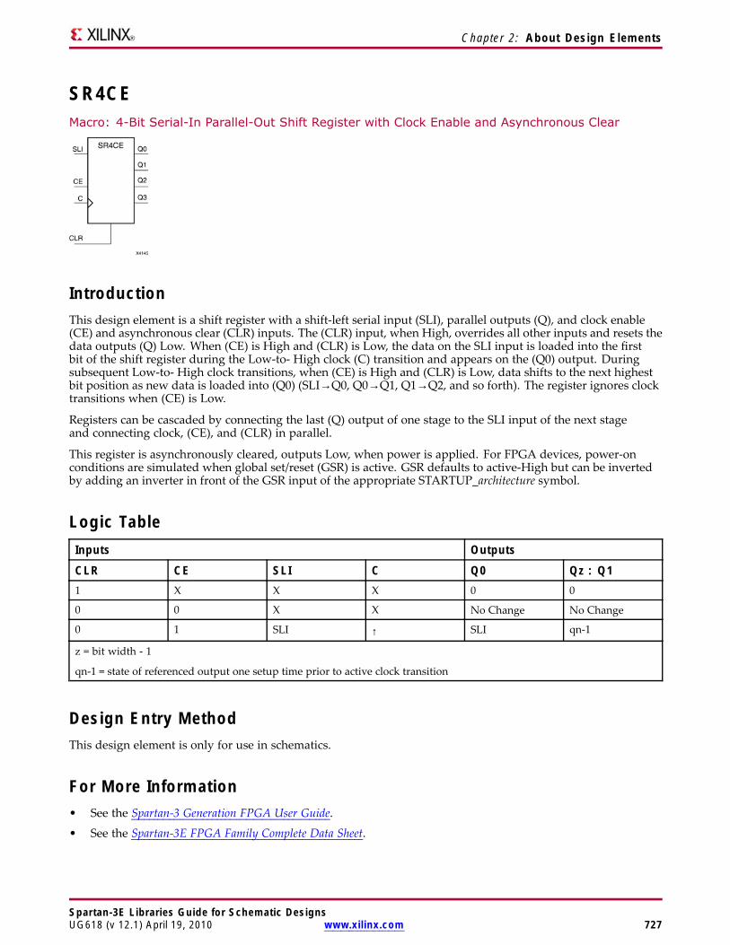
Chapter 2: About Design Elements
SR4CEMacro: 4-Bit Serial-In Parallel-Out Shift Register with Clock Enable and Asynchronous Clear
IntroductionThis design element is a shift register with a shift-left serial input (SLI), parallel outputs (Q), and clock enable(CE) and asynchronous clear (CLR) inputs. The (CLR) input, when High, overrides all other inputs and resets thedata outputs (Q) Low. When (CE) is High and (CLR) is Low, the data on the SLI input is loaded into the firstbit of the shift register during the Low-to- High clock (C) transition and appears on the (Q0) output. Duringsubsequent Low-to- High clock transitions, when (CE) is High and (CLR) is Low, data shifts to the next highestbit position as new data is loaded into (Q0) (SLI→Q0, Q0→Q1, Q1→Q2, and so forth). The register ignores clocktransitions when (CE) is Low.
Registers can be cascaded by connecting the last (Q) output of one stage to the SLI input of the next stageand connecting clock, (CE), and (CLR) in parallel.
This register is asynchronously cleared, outputs Low, when power is applied. For FPGA devices, power-onconditions are simulated when global set/reset (GSR) is active. GSR defaults to active-High but can be invertedby adding an inverter in front of the GSR input of the appropriate STARTUP_architecture symbol.
Logic TableInputs Outputs
CLR CE SLI C Q0 Qz : Q11 X X X 0 0
0 0 X X No Change No Change
0 1 SLI ↑ SLI qn-1
z = bit width - 1
qn-1 = state of referenced output one setup time prior to active clock transition
Design Entry MethodThis design element is only for use in schematics.
For More Information• See the Spartan-3 Generation FPGA User Guide.
• See the Spartan-3E FPGA Family Complete Data Sheet.
Spartan-3E Libraries Guide for Schematic DesignsUG618 (v 12.1) April 19, 2010 www.xilinx.com 727
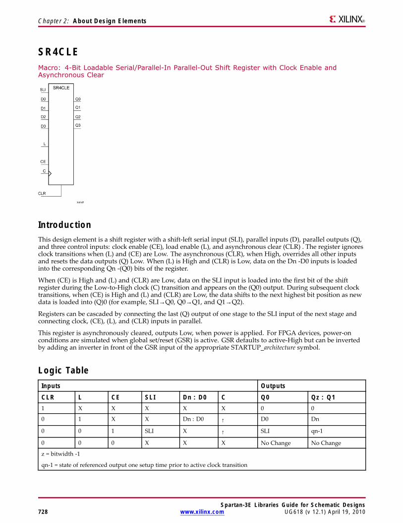
Chapter 2: About Design Elements
SR4CLEMacro: 4-Bit Loadable Serial/Parallel-In Parallel-Out Shift Register with Clock Enable andAsynchronous Clear
IntroductionThis design element is a shift register with a shift-left serial input (SLI), parallel inputs (D), parallel outputs (Q),and three control inputs: clock enable (CE), load enable (L), and asynchronous clear (CLR) . The register ignoresclock transitions when (L) and (CE) are Low. The asynchronous (CLR), when High, overrides all other inputsand resets the data outputs (Q) Low. When (L) is High and (CLR) is Low, data on the Dn -D0 inputs is loadedinto the corresponding Qn -(Q0) bits of the register.
When (CE) is High and (L) and (CLR) are Low, data on the SLI input is loaded into the first bit of the shiftregister during the Low-to-High clock (C) transition and appears on the (Q0) output. During subsequent clocktransitions, when (CE) is High and (L) and (CLR) are Low, the data shifts to the next highest bit position as newdata is loaded into (Q)0 (for example, SLI→Q0, Q0→Q1, and Q1→Q2).
Registers can be cascaded by connecting the last (Q) output of one stage to the SLI input of the next stage andconnecting clock, (CE), (L), and (CLR) inputs in parallel.
This register is asynchronously cleared, outputs Low, when power is applied. For FPGA devices, power-onconditions are simulated when global set/reset (GSR) is active. GSR defaults to active-High but can be invertedby adding an inverter in front of the GSR input of the appropriate STARTUP_architecture symbol.
Logic TableInputs Outputs
CLR L CE SLI Dn : D0 C Q0 Qz : Q11 X X X X X 0 0
0 1 X X Dn : D0 ↑ D0 Dn
0 0 1 SLI X ↑ SLI qn-1
0 0 0 X X X No Change No Change
z = bitwidth -1
qn-1 = state of referenced output one setup time prior to active clock transition
Spartan-3E Libraries Guide for Schematic Designs728 www.xilinx.com UG618 (v 12.1) April 19, 2010

Chapter 2: About Design Elements
Design Entry MethodThis design element is only for use in schematics.
For More Information• See the Spartan-3 Generation FPGA User Guide.
• See the Spartan-3E FPGA Family Complete Data Sheet.
Spartan-3E Libraries Guide for Schematic DesignsUG618 (v 12.1) April 19, 2010 www.xilinx.com 729
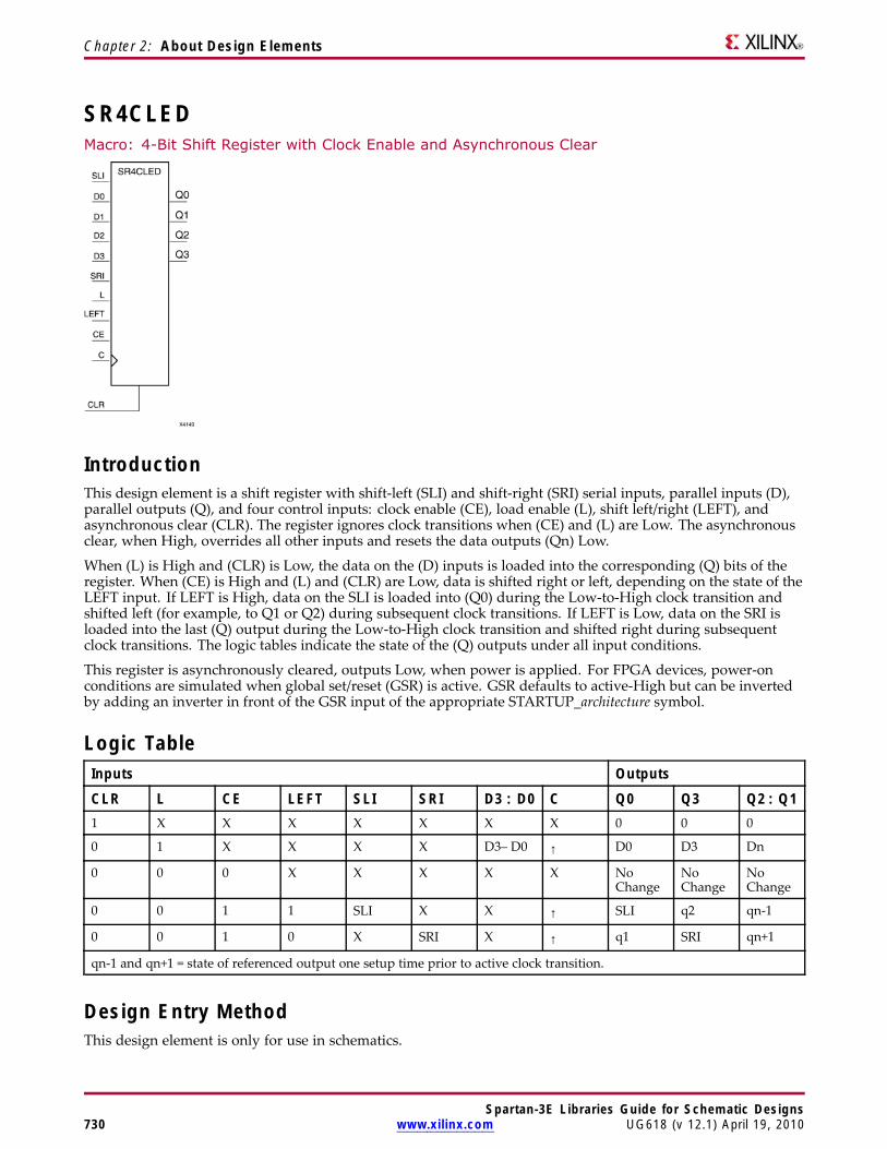
Chapter 2: About Design Elements
SR4CLEDMacro: 4-Bit Shift Register with Clock Enable and Asynchronous Clear
IntroductionThis design element is a shift register with shift-left (SLI) and shift-right (SRI) serial inputs, parallel inputs (D),parallel outputs (Q), and four control inputs: clock enable (CE), load enable (L), shift left/right (LEFT), andasynchronous clear (CLR). The register ignores clock transitions when (CE) and (L) are Low. The asynchronousclear, when High, overrides all other inputs and resets the data outputs (Qn) Low.
When (L) is High and (CLR) is Low, the data on the (D) inputs is loaded into the corresponding (Q) bits of theregister. When (CE) is High and (L) and (CLR) are Low, data is shifted right or left, depending on the state of theLEFT input. If LEFT is High, data on the SLI is loaded into (Q0) during the Low-to-High clock transition andshifted left (for example, to Q1 or Q2) during subsequent clock transitions. If LEFT is Low, data on the SRI isloaded into the last (Q) output during the Low-to-High clock transition and shifted right during subsequentclock transitions. The logic tables indicate the state of the (Q) outputs under all input conditions.
This register is asynchronously cleared, outputs Low, when power is applied. For FPGA devices, power-onconditions are simulated when global set/reset (GSR) is active. GSR defaults to active-High but can be invertedby adding an inverter in front of the GSR input of the appropriate STARTUP_architecture symbol.
Logic TableInputs Outputs
CLR L CE LEFT SLI SRI D3 : D0 C Q0 Q3 Q2 : Q11 X X X X X X X 0 0 0
0 1 X X X X D3– D0 ↑ D0 D3 Dn
0 0 0 X X X X X NoChange
NoChange
NoChange
0 0 1 1 SLI X X ↑ SLI q2 qn-1
0 0 1 0 X SRI X ↑ q1 SRI qn+1
qn-1 and qn+1 = state of referenced output one setup time prior to active clock transition.
Design Entry MethodThis design element is only for use in schematics.
Spartan-3E Libraries Guide for Schematic Designs730 www.xilinx.com UG618 (v 12.1) April 19, 2010

Chapter 2: About Design Elements
For More Information• See the Spartan-3 Generation FPGA User Guide.
• See the Spartan-3E FPGA Family Complete Data Sheet.
Spartan-3E Libraries Guide for Schematic DesignsUG618 (v 12.1) April 19, 2010 www.xilinx.com 731
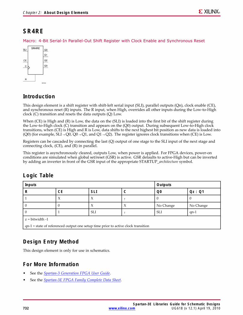
Chapter 2: About Design Elements
SR4REMacro: 4-Bit Serial-In Parallel-Out Shift Register with Clock Enable and Synchronous Reset
IntroductionThis design element is a shift register with shift-left serial input (SLI), parallel outputs (Qn), clock enable (CE),and synchronous reset (R) inputs. The R input, when High, overrides all other inputs during the Low-to-Highclock (C) transition and resets the data outputs (Q) Low.
When (CE) is High and (R) is Low, the data on the (SLI) is loaded into the first bit of the shift register duringthe Low-to-High clock (C) transition and appears on the (Q0) output. During subsequent Low-to-High clocktransitions, when (CE) is High and R is Low, data shifts to the next highest bit position as new data is loaded into(Q0) (for example, SLI→Q0, Q0→Q1, and Q1→Q2). The register ignores clock transitions when (CE) is Low.
Registers can be cascaded by connecting the last (Q) output of one stage to the SLI input of the next stage andconnecting clock, (CE), and (R) in parallel.
This register is asynchronously cleared, outputs Low, when power is applied. For FPGA devices, power-onconditions are simulated when global set/reset (GSR) is active. GSR defaults to active-High but can be invertedby adding an inverter in front of the GSR input of the appropriate STARTUP_architecture symbol.
Logic TableInputs Outputs
R CE SLI C Q0 Qz : Q11 X X ↑ 0 0
0 0 X X No Change No Change
0 1 SLI ↑ SLI qn-1
z = bitwidth -1
qn-1 = state of referenced output one setup time prior to active clock transition
Design Entry MethodThis design element is only for use in schematics.
For More Information• See the Spartan-3 Generation FPGA User Guide.
• See the Spartan-3E FPGA Family Complete Data Sheet.
Spartan-3E Libraries Guide for Schematic Designs732 www.xilinx.com UG618 (v 12.1) April 19, 2010
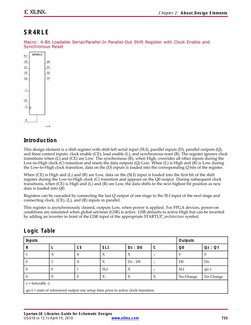
Chapter 2: About Design Elements
SR4RLEMacro: 4-Bit Loadable Serial/Parallel-In Parallel-Out Shift Register with Clock Enable andSynchronous Reset
IntroductionThis design element is a shift register with shift-left serial input (SLI), parallel inputs (D), parallel outputs (Q),and three control inputs: clock enable (CE), load enable (L), and synchronous reset (R). The register ignores clocktransitions when (L) and (CE) are Low. The synchronous (R), when High, overrides all other inputs during theLow-to-High clock (C) transition and resets the data outputs (Q) Low. When (L) is High and (R) is Low duringthe Low-to-High clock transition, data on the (D) inputs is loaded into the corresponding Q bits of the register.
When (CE) is High and (L) and (R) are Low, data on the (SLI) input is loaded into the first bit of the shiftregister during the Low-to-High clock (C) transition and appears on the Q0 output. During subsequent clocktransitions, when (CE) is High and (L) and (R) are Low, the data shifts to the next highest bit position as newdata is loaded into Q0.
Registers can be cascaded by connecting the last Q output of one stage to the SLI input of the next stage andconnecting clock, (CE), (L), and (R) inputs in parallel.
This register is asynchronously cleared, outputs Low, when power is applied. For FPGA devices, power-onconditions are simulated when global set/reset (GSR) is active. GSR defaults to active-High but can be invertedby adding an inverter in front of the GSR input of the appropriate STARTUP_architecture symbol.
Logic TableInputs Outputs
R L CE SLI Dz : D0 C Q0 Qz : Q11 X X X X ↑ 0 0
0 1 X X Dz : D0 ↑ D0 Dn
0 0 1 SLI X ↑ SLI qn-1
0 0 0 X X X No Change No Change
z = bitwidth -1
qn-1 = state of referenced output one setup time prior to active clock transition
Spartan-3E Libraries Guide for Schematic DesignsUG618 (v 12.1) April 19, 2010 www.xilinx.com 733

Chapter 2: About Design Elements
Design Entry MethodThis design element is only for use in schematics.
For More Information• See the Spartan-3 Generation FPGA User Guide.
• See the Spartan-3E FPGA Family Complete Data Sheet.
Spartan-3E Libraries Guide for Schematic Designs734 www.xilinx.com UG618 (v 12.1) April 19, 2010
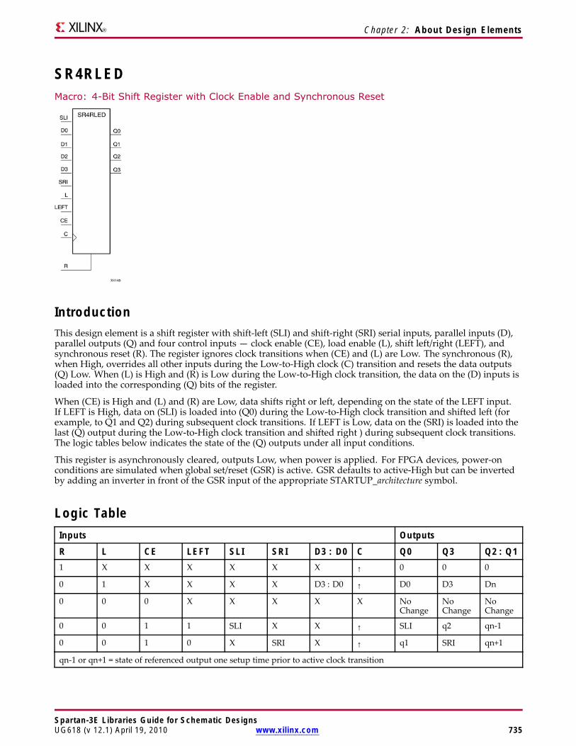
Chapter 2: About Design Elements
SR4RLEDMacro: 4-Bit Shift Register with Clock Enable and Synchronous Reset
IntroductionThis design element is a shift register with shift-left (SLI) and shift-right (SRI) serial inputs, parallel inputs (D),parallel outputs (Q) and four control inputs — clock enable (CE), load enable (L), shift left/right (LEFT), andsynchronous reset (R). The register ignores clock transitions when (CE) and (L) are Low. The synchronous (R),when High, overrides all other inputs during the Low-to-High clock (C) transition and resets the data outputs(Q) Low. When (L) is High and (R) is Low during the Low-to-High clock transition, the data on the (D) inputs isloaded into the corresponding (Q) bits of the register.
When (CE) is High and (L) and (R) are Low, data shifts right or left, depending on the state of the LEFT input.If LEFT is High, data on (SLI) is loaded into (Q0) during the Low-to-High clock transition and shifted left (forexample, to Q1 and Q2) during subsequent clock transitions. If LEFT is Low, data on the (SRI) is loaded into thelast (Q) output during the Low-to-High clock transition and shifted right ) during subsequent clock transitions.The logic tables below indicates the state of the (Q) outputs under all input conditions.
This register is asynchronously cleared, outputs Low, when power is applied. For FPGA devices, power-onconditions are simulated when global set/reset (GSR) is active. GSR defaults to active-High but can be invertedby adding an inverter in front of the GSR input of the appropriate STARTUP_architecture symbol.
Logic TableInputs Outputs
R L CE LEFT SLI SRI D3 : D0 C Q0 Q3 Q2 : Q11 X X X X X X ↑ 0 0 0
0 1 X X X X D3 : D0 ↑ D0 D3 Dn
0 0 0 X X X X X NoChange
NoChange
NoChange
0 0 1 1 SLI X X ↑ SLI q2 qn-1
0 0 1 0 X SRI X ↑ q1 SRI qn+1
qn-1 or qn+1 = state of referenced output one setup time prior to active clock transition
Spartan-3E Libraries Guide for Schematic DesignsUG618 (v 12.1) April 19, 2010 www.xilinx.com 735

Chapter 2: About Design Elements
Design Entry MethodThis design element is only for use in schematics.
For More Information• See the Spartan-3 Generation FPGA User Guide.
• See the Spartan-3E FPGA Family Complete Data Sheet.
Spartan-3E Libraries Guide for Schematic Designs736 www.xilinx.com UG618 (v 12.1) April 19, 2010

Chapter 2: About Design Elements
SR8CEMacro: 8-Bit Serial-In Parallel-Out Shift Register with Clock Enable and Asynchronous Clear
IntroductionThis design element is a shift register with a shift-left serial input (SLI), parallel outputs (Q), and clock enable(CE) and asynchronous clear (CLR) inputs. The (CLR) input, when High, overrides all other inputs and resets thedata outputs (Q) Low. When (CE) is High and (CLR) is Low, the data on the SLI input is loaded into the firstbit of the shift register during the Low-to- High clock (C) transition and appears on the (Q0) output. Duringsubsequent Low-to- High clock transitions, when (CE) is High and (CLR) is Low, data shifts to the next highestbit position as new data is loaded into (Q0) (SLI→Q0, Q0→Q1, Q1→Q2, and so forth). The register ignores clocktransitions when (CE) is Low.
Registers can be cascaded by connecting the last (Q) output of one stage to the SLI input of the next stageand connecting clock, (CE), and (CLR) in parallel.
This register is asynchronously cleared, outputs Low, when power is applied. For FPGA devices, power-onconditions are simulated when global set/reset (GSR) is active. GSR defaults to active-High but can be invertedby adding an inverter in front of the GSR input of the appropriate STARTUP_architecture symbol.
Logic TableInputs Outputs
CLR CE SLI C Q0 Qz : Q11 X X X 0 0
0 0 X X No Change No Change
0 1 SLI ↑ SLI qn-1
z = bit width - 1
qn-1 = state of referenced output one setup time prior to active clock transition
Design Entry MethodThis design element is only for use in schematics.
For More Information• See the Spartan-3 Generation FPGA User Guide.
• See the Spartan-3E FPGA Family Complete Data Sheet.
Spartan-3E Libraries Guide for Schematic DesignsUG618 (v 12.1) April 19, 2010 www.xilinx.com 737

Chapter 2: About Design Elements
SR8CLEMacro: 8-Bit Loadable Serial/Parallel-In Parallel-Out Shift Register with Clock Enable andAsynchronous Clear
IntroductionThis design element is a shift register with a shift-left serial input (SLI), parallel inputs (D), parallel outputs (Q),and three control inputs: clock enable (CE), load enable (L), and asynchronous clear (CLR) . The register ignoresclock transitions when (L) and (CE) are Low. The asynchronous (CLR), when High, overrides all other inputsand resets the data outputs (Q) Low. When (L) is High and (CLR) is Low, data on the Dn -D0 inputs is loadedinto the corresponding Qn -(Q0) bits of the register.
When (CE) is High and (L) and (CLR) are Low, data on the SLI input is loaded into the first bit of the shiftregister during the Low-to-High clock (C) transition and appears on the (Q0) output. During subsequent clocktransitions, when (CE) is High and (L) and (CLR) are Low, the data shifts to the next highest bit position as newdata is loaded into (Q)0 (for example, SLI→Q0, Q0→Q1, and Q1→Q2).
Registers can be cascaded by connecting the last (Q) output of one stage to the SLI input of the next stage andconnecting clock, (CE), (L), and (CLR) inputs in parallel.
This register is asynchronously cleared, outputs Low, when power is applied. For FPGA devices, power-onconditions are simulated when global set/reset (GSR) is active. GSR defaults to active-High but can be invertedby adding an inverter in front of the GSR input of the appropriate STARTUP_architecture symbol.
Logic TableInputs Outputs
CLR L CE SLI Dn : D0 C Q0 Qz : Q11 X X X X X 0 0
0 1 X X Dn : D0 ↑ D0 Dn
0 0 1 SLI X ↑ SLI qn-1
0 0 0 X X X No Change No Change
z = bitwidth -1
qn-1 = state of referenced output one setup time prior to active clock transition
Design Entry MethodThis design element is only for use in schematics.
Spartan-3E Libraries Guide for Schematic Designs738 www.xilinx.com UG618 (v 12.1) April 19, 2010

Chapter 2: About Design Elements
For More Information• See the Spartan-3 Generation FPGA User Guide.
• See the Spartan-3E FPGA Family Complete Data Sheet.
Spartan-3E Libraries Guide for Schematic DesignsUG618 (v 12.1) April 19, 2010 www.xilinx.com 739
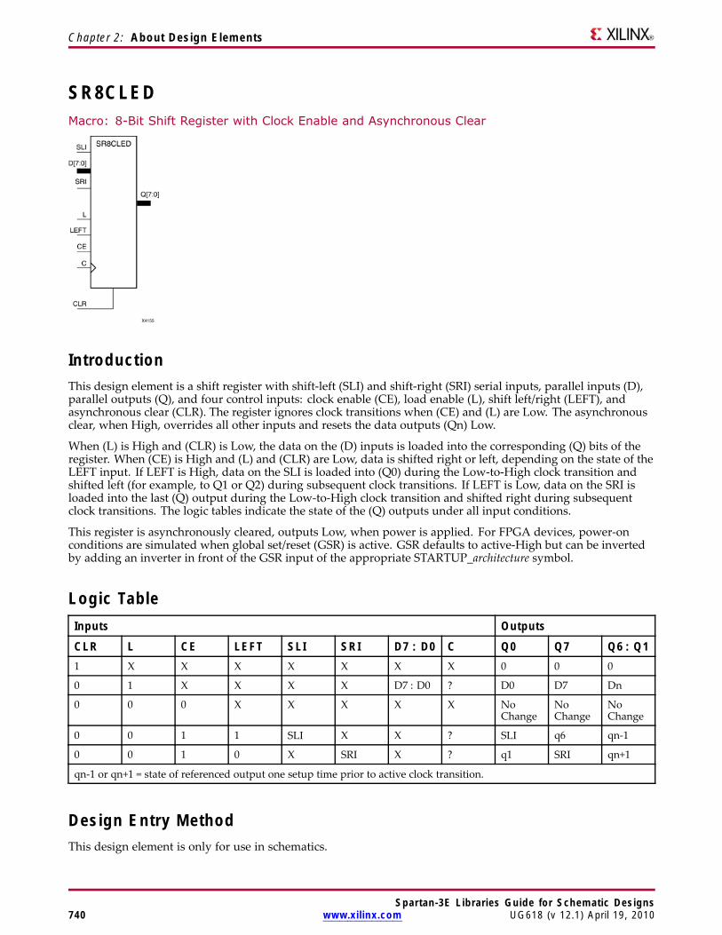
Chapter 2: About Design Elements
SR8CLEDMacro: 8-Bit Shift Register with Clock Enable and Asynchronous Clear
IntroductionThis design element is a shift register with shift-left (SLI) and shift-right (SRI) serial inputs, parallel inputs (D),parallel outputs (Q), and four control inputs: clock enable (CE), load enable (L), shift left/right (LEFT), andasynchronous clear (CLR). The register ignores clock transitions when (CE) and (L) are Low. The asynchronousclear, when High, overrides all other inputs and resets the data outputs (Qn) Low.
When (L) is High and (CLR) is Low, the data on the (D) inputs is loaded into the corresponding (Q) bits of theregister. When (CE) is High and (L) and (CLR) are Low, data is shifted right or left, depending on the state of theLEFT input. If LEFT is High, data on the SLI is loaded into (Q0) during the Low-to-High clock transition andshifted left (for example, to Q1 or Q2) during subsequent clock transitions. If LEFT is Low, data on the SRI isloaded into the last (Q) output during the Low-to-High clock transition and shifted right during subsequentclock transitions. The logic tables indicate the state of the (Q) outputs under all input conditions.
This register is asynchronously cleared, outputs Low, when power is applied. For FPGA devices, power-onconditions are simulated when global set/reset (GSR) is active. GSR defaults to active-High but can be invertedby adding an inverter in front of the GSR input of the appropriate STARTUP_architecture symbol.
Logic TableInputs Outputs
CLR L CE LEFT SLI SRI D7 : D0 C Q0 Q7 Q6 : Q11 X X X X X X X 0 0 0
0 1 X X X X D7 : D0 ? D0 D7 Dn
0 0 0 X X X X X NoChange
NoChange
NoChange
0 0 1 1 SLI X X ? SLI q6 qn-1
0 0 1 0 X SRI X ? q1 SRI qn+1
qn-1 or qn+1 = state of referenced output one setup time prior to active clock transition.
Design Entry MethodThis design element is only for use in schematics.
Spartan-3E Libraries Guide for Schematic Designs740 www.xilinx.com UG618 (v 12.1) April 19, 2010

Chapter 2: About Design Elements
For More Information• See the Spartan-3 Generation FPGA User Guide.
• See the Spartan-3E FPGA Family Complete Data Sheet.
Spartan-3E Libraries Guide for Schematic DesignsUG618 (v 12.1) April 19, 2010 www.xilinx.com 741
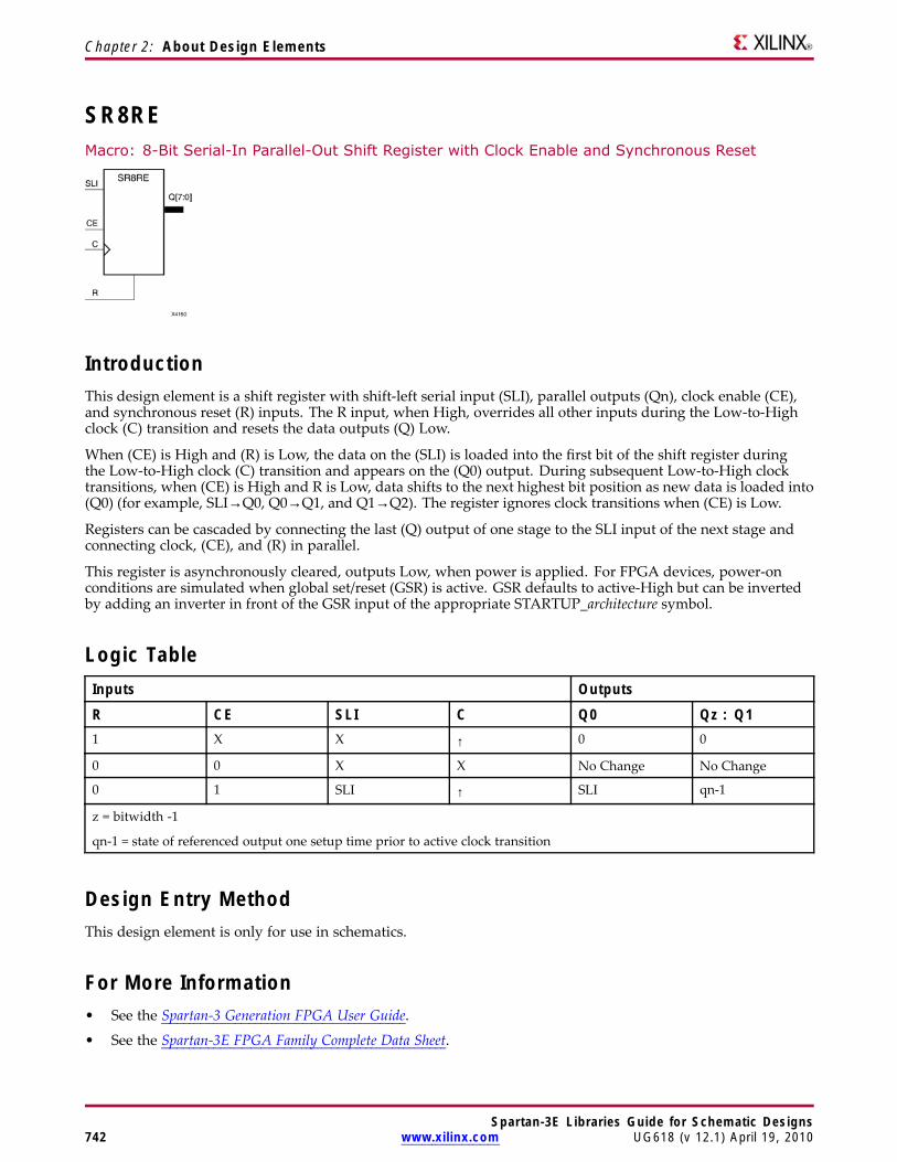
Chapter 2: About Design Elements
SR8REMacro: 8-Bit Serial-In Parallel-Out Shift Register with Clock Enable and Synchronous Reset
IntroductionThis design element is a shift register with shift-left serial input (SLI), parallel outputs (Qn), clock enable (CE),and synchronous reset (R) inputs. The R input, when High, overrides all other inputs during the Low-to-Highclock (C) transition and resets the data outputs (Q) Low.
When (CE) is High and (R) is Low, the data on the (SLI) is loaded into the first bit of the shift register duringthe Low-to-High clock (C) transition and appears on the (Q0) output. During subsequent Low-to-High clocktransitions, when (CE) is High and R is Low, data shifts to the next highest bit position as new data is loaded into(Q0) (for example, SLI→Q0, Q0→Q1, and Q1→Q2). The register ignores clock transitions when (CE) is Low.
Registers can be cascaded by connecting the last (Q) output of one stage to the SLI input of the next stage andconnecting clock, (CE), and (R) in parallel.
This register is asynchronously cleared, outputs Low, when power is applied. For FPGA devices, power-onconditions are simulated when global set/reset (GSR) is active. GSR defaults to active-High but can be invertedby adding an inverter in front of the GSR input of the appropriate STARTUP_architecture symbol.
Logic TableInputs Outputs
R CE SLI C Q0 Qz : Q11 X X ↑ 0 0
0 0 X X No Change No Change
0 1 SLI ↑ SLI qn-1
z = bitwidth -1
qn-1 = state of referenced output one setup time prior to active clock transition
Design Entry MethodThis design element is only for use in schematics.
For More Information• See the Spartan-3 Generation FPGA User Guide.
• See the Spartan-3E FPGA Family Complete Data Sheet.
Spartan-3E Libraries Guide for Schematic Designs742 www.xilinx.com UG618 (v 12.1) April 19, 2010
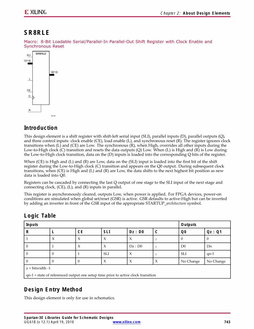
Chapter 2: About Design Elements
SR8RLEMacro: 8-Bit Loadable Serial/Parallel-In Parallel-Out Shift Register with Clock Enable andSynchronous Reset
IntroductionThis design element is a shift register with shift-left serial input (SLI), parallel inputs (D), parallel outputs (Q),and three control inputs: clock enable (CE), load enable (L), and synchronous reset (R). The register ignores clocktransitions when (L) and (CE) are Low. The synchronous (R), when High, overrides all other inputs during theLow-to-High clock (C) transition and resets the data outputs (Q) Low. When (L) is High and (R) is Low duringthe Low-to-High clock transition, data on the (D) inputs is loaded into the corresponding Q bits of the register.
When (CE) is High and (L) and (R) are Low, data on the (SLI) input is loaded into the first bit of the shiftregister during the Low-to-High clock (C) transition and appears on the Q0 output. During subsequent clocktransitions, when (CE) is High and (L) and (R) are Low, the data shifts to the next highest bit position as newdata is loaded into Q0.
Registers can be cascaded by connecting the last Q output of one stage to the SLI input of the next stage andconnecting clock, (CE), (L), and (R) inputs in parallel.
This register is asynchronously cleared, outputs Low, when power is applied. For FPGA devices, power-onconditions are simulated when global set/reset (GSR) is active. GSR defaults to active-High but can be invertedby adding an inverter in front of the GSR input of the appropriate STARTUP_architecture symbol.
Logic TableInputs Outputs
R L CE SLI Dz : D0 C Q0 Qz : Q11 X X X X ↑ 0 0
0 1 X X Dz : D0 ↑ D0 Dn
0 0 1 SLI X ↑ SLI qn-1
0 0 0 X X X No Change No Change
z = bitwidth -1
qn-1 = state of referenced output one setup time prior to active clock transition
Design Entry MethodThis design element is only for use in schematics.
Spartan-3E Libraries Guide for Schematic DesignsUG618 (v 12.1) April 19, 2010 www.xilinx.com 743

Chapter 2: About Design Elements
For More Information• See the Spartan-3 Generation FPGA User Guide.
• See the Spartan-3E FPGA Family Complete Data Sheet.
Spartan-3E Libraries Guide for Schematic Designs744 www.xilinx.com UG618 (v 12.1) April 19, 2010
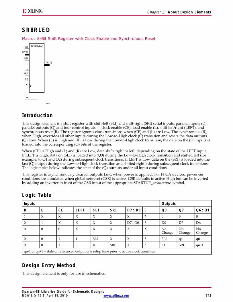
Chapter 2: About Design Elements
SR8RLEDMacro: 8-Bit Shift Register with Clock Enable and Synchronous Reset
IntroductionThis design element is a shift register with shift-left (SLI) and shift-right (SRI) serial inputs, parallel inputs (D),parallel outputs (Q) and four control inputs — clock enable (CE), load enable (L), shift left/right (LEFT), andsynchronous reset (R). The register ignores clock transitions when (CE) and (L) are Low. The synchronous (R),when High, overrides all other inputs during the Low-to-High clock (C) transition and resets the data outputs(Q) Low. When (L) is High and (R) is Low during the Low-to-High clock transition, the data on the (D) inputs isloaded into the corresponding (Q) bits of the register.
When (CE) is High and (L) and (R) are Low, data shifts right or left, depending on the state of the LEFT input.If LEFT is High, data on (SLI) is loaded into (Q0) during the Low-to-High clock transition and shifted left (forexample, to Q1 and Q2) during subsequent clock transitions. If LEFT is Low, data on the (SRI) is loaded into thelast (Q) output during the Low-to-High clock transition and shifted right ) during subsequent clock transitions.The logic tables below indicates the state of the (Q) outputs under all input conditions.
This register is asynchronously cleared, outputs Low, when power is applied. For FPGA devices, power-onconditions are simulated when global set/reset (GSR) is active. GSR defaults to active-High but can be invertedby adding an inverter in front of the GSR input of the appropriate STARTUP_architecture symbol.
Logic TableInputs Outputs
R L CE LEFT SLI SRI D7 : D0 C Q0 Q7 Q6 : Q11 X X X X X X ? 0 0 0
0 1 X X X X D7 : D0 ? D0 D7 Dn
0 0 0 X X X X X NoChange
NoChange
NoChange
0 0 1 1 SLI X X ? SLI q6 qn-1
0 0 1 0 X SRI X ? q1 SRI qn+1
qn-1 or qn+1 = state of referenced output one setup time prior to active clock transition
Design Entry MethodThis design element is only for use in schematics.
Spartan-3E Libraries Guide for Schematic DesignsUG618 (v 12.1) April 19, 2010 www.xilinx.com 745

Chapter 2: About Design Elements
For More Information• See the Spartan-3 Generation FPGA User Guide.
• See the Spartan-3E FPGA Family Complete Data Sheet.
Spartan-3E Libraries Guide for Schematic Designs746 www.xilinx.com UG618 (v 12.1) April 19, 2010
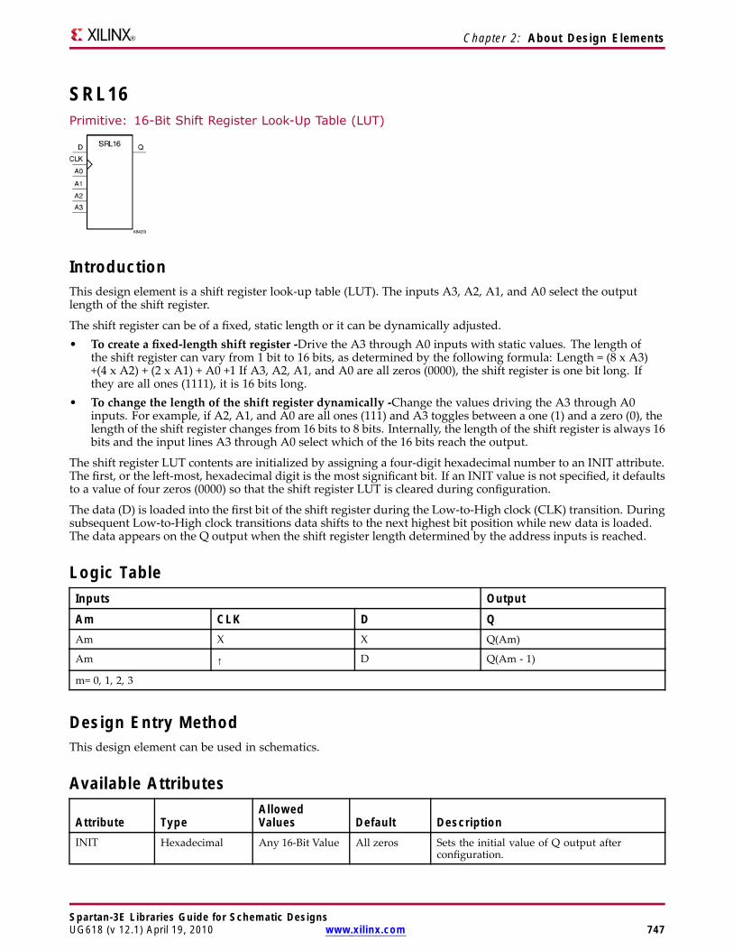
Chapter 2: About Design Elements
SRL16Primitive: 16-Bit Shift Register Look-Up Table (LUT)
IntroductionThis design element is a shift register look-up table (LUT). The inputs A3, A2, A1, and A0 select the outputlength of the shift register.
The shift register can be of a fixed, static length or it can be dynamically adjusted.• To create a fixed-length shift register -Drive the A3 through A0 inputs with static values. The length of
the shift register can vary from 1 bit to 16 bits, as determined by the following formula: Length = (8 x A3)+(4 x A2) + (2 x A1) + A0 +1 If A3, A2, A1, and A0 are all zeros (0000), the shift register is one bit long. Ifthey are all ones (1111), it is 16 bits long.
• To change the length of the shift register dynamically -Change the values driving the A3 through A0inputs. For example, if A2, A1, and A0 are all ones (111) and A3 toggles between a one (1) and a zero (0), thelength of the shift register changes from 16 bits to 8 bits. Internally, the length of the shift register is always 16bits and the input lines A3 through A0 select which of the 16 bits reach the output.
The shift register LUT contents are initialized by assigning a four-digit hexadecimal number to an INIT attribute.The first, or the left-most, hexadecimal digit is the most significant bit. If an INIT value is not specified, it defaultsto a value of four zeros (0000) so that the shift register LUT is cleared during configuration.
The data (D) is loaded into the first bit of the shift register during the Low-to-High clock (CLK) transition. Duringsubsequent Low-to-High clock transitions data shifts to the next highest bit position while new data is loaded.The data appears on the Q output when the shift register length determined by the address inputs is reached.
Logic TableInputs Output
Am CLK D QAm X X Q(Am)
Am ↑ D Q(Am - 1)
m= 0, 1, 2, 3
Design Entry MethodThis design element can be used in schematics.
Available Attributes
Attribute TypeAllowedValues Default Description
INIT Hexadecimal Any 16-Bit Value All zeros Sets the initial value of Q output afterconfiguration.
Spartan-3E Libraries Guide for Schematic DesignsUG618 (v 12.1) April 19, 2010 www.xilinx.com 747

Chapter 2: About Design Elements
For More Information• See the Spartan-3 Generation FPGA User Guide.
• See the Spartan-3E FPGA Family Complete Data Sheet.
Spartan-3E Libraries Guide for Schematic Designs748 www.xilinx.com UG618 (v 12.1) April 19, 2010
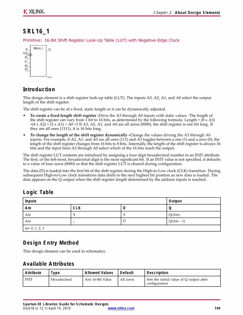
Chapter 2: About Design Elements
SRL16_1Primitive: 16-Bit Shift Register Look-Up Table (LUT) with Negative-Edge Clock
IntroductionThis design element is a shift register look-up table (LUT). The inputs A3, A2, A1, and A0 select the outputlength of the shift register.
The shift register can be of a fixed, static length or it can be dynamically adjusted.• To create a fixed-length shift register -Drive the A3 through A0 inputs with static values. The length of
the shift register can vary from 1 bit to 16 bits, as determined by the following formula: Length = (8 x A3)+(4 x A2) + (2 x A1) + A0 +1 If A3, A2, A1, and A0 are all zeros (0000), the shift register is one bit long. Ifthey are all ones (1111), it is 16 bits long.
• To change the length of the shift register dynamically -Change the values driving the A3 through A0inputs. For example, if A2, A1, and A0 are all ones (111) and A3 toggles between a one (1) and a zero (0), thelength of the shift register changes from 16 bits to 8 bits. Internally, the length of the shift register is always 16bits and the input lines A3 through A0 select which of the 16 bits reach the output.
The shift register LUT contents are initialized by assigning a four-digit hexadecimal number to an INIT attribute.The first, or the left-most, hexadecimal digit is the most significant bit. If an INIT value is not specified, it defaultsto a value of four zeros (0000) so that the shift register LUT is cleared during configuration.
The data (D) is loaded into the first bit of the shift register during the High-to-Low clock (CLK) transition. Duringsubsequent High-to-Low clock transitions data shifts to the next highest bit position as new data is loaded. Thedata appears on the Q output when the shift register length determined by the address inputs is reached.
Logic TableInputs Output
Am CLK D QAm X X Q(Am)
Am ↓ D Q(Am - 1)
m= 0, 1, 2, 3
Design Entry MethodThis design element can be used in schematics.
Available AttributesAttribute Type Allowed Values Default DescriptionINIT Hexadecimal Any 16-Bit Value All zeros Sets the initial value of Q output after
configuration
Spartan-3E Libraries Guide for Schematic DesignsUG618 (v 12.1) April 19, 2010 www.xilinx.com 749

Chapter 2: About Design Elements
For More Information• See the Spartan-3 Generation FPGA User Guide.
• See the Spartan-3E FPGA Family Complete Data Sheet.
Spartan-3E Libraries Guide for Schematic Designs750 www.xilinx.com UG618 (v 12.1) April 19, 2010
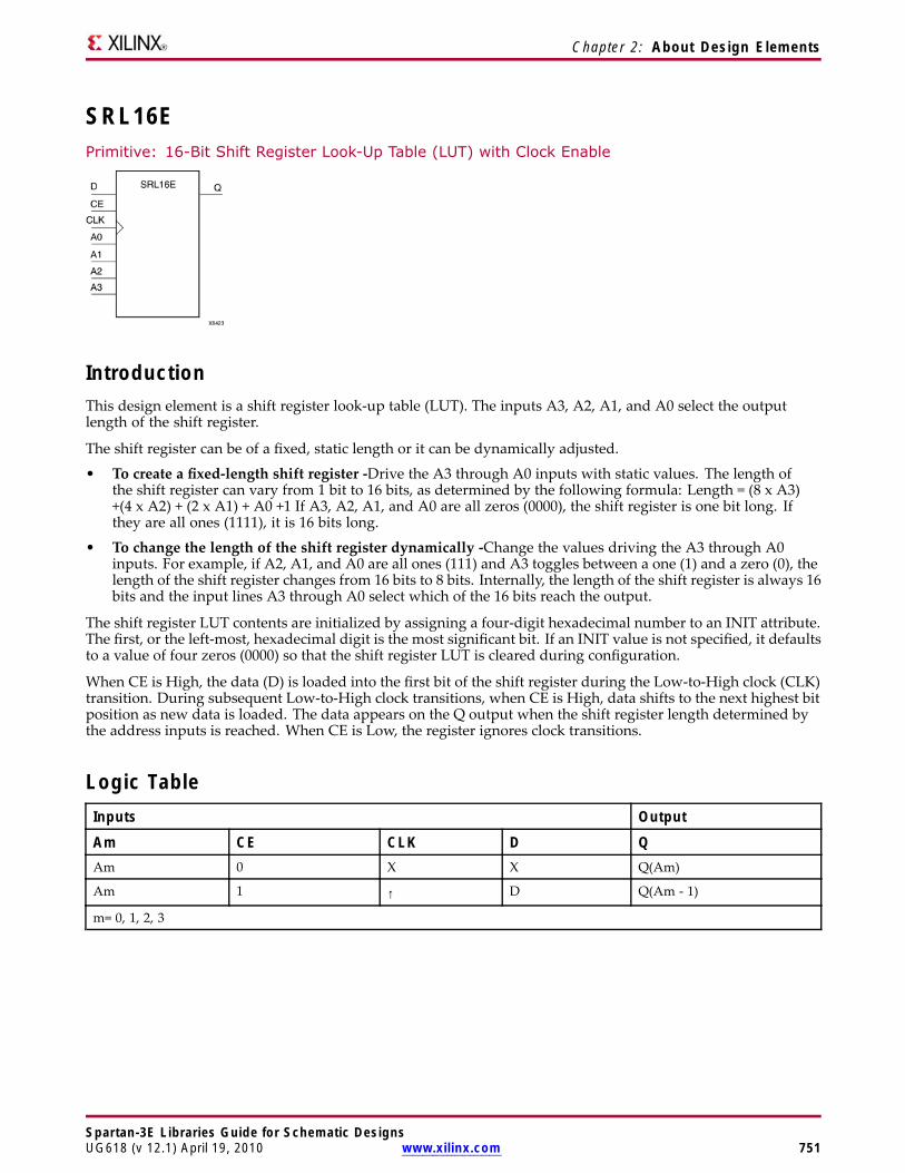
Chapter 2: About Design Elements
SRL16EPrimitive: 16-Bit Shift Register Look-Up Table (LUT) with Clock Enable
IntroductionThis design element is a shift register look-up table (LUT). The inputs A3, A2, A1, and A0 select the outputlength of the shift register.
The shift register can be of a fixed, static length or it can be dynamically adjusted.
• To create a fixed-length shift register -Drive the A3 through A0 inputs with static values. The length ofthe shift register can vary from 1 bit to 16 bits, as determined by the following formula: Length = (8 x A3)+(4 x A2) + (2 x A1) + A0 +1 If A3, A2, A1, and A0 are all zeros (0000), the shift register is one bit long. Ifthey are all ones (1111), it is 16 bits long.
• To change the length of the shift register dynamically -Change the values driving the A3 through A0inputs. For example, if A2, A1, and A0 are all ones (111) and A3 toggles between a one (1) and a zero (0), thelength of the shift register changes from 16 bits to 8 bits. Internally, the length of the shift register is always 16bits and the input lines A3 through A0 select which of the 16 bits reach the output.
The shift register LUT contents are initialized by assigning a four-digit hexadecimal number to an INIT attribute.The first, or the left-most, hexadecimal digit is the most significant bit. If an INIT value is not specified, it defaultsto a value of four zeros (0000) so that the shift register LUT is cleared during configuration.
When CE is High, the data (D) is loaded into the first bit of the shift register during the Low-to-High clock (CLK)transition. During subsequent Low-to-High clock transitions, when CE is High, data shifts to the next highest bitposition as new data is loaded. The data appears on the Q output when the shift register length determined bythe address inputs is reached. When CE is Low, the register ignores clock transitions.
Logic TableInputs Output
Am CE CLK D QAm 0 X X Q(Am)
Am 1 ↑ D Q(Am - 1)
m= 0, 1, 2, 3
Spartan-3E Libraries Guide for Schematic DesignsUG618 (v 12.1) April 19, 2010 www.xilinx.com 751
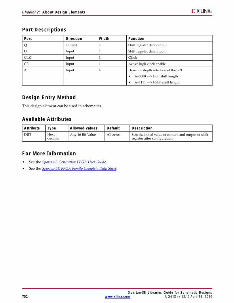
Chapter 2: About Design Elements
Port DescriptionsPort Direction Width FunctionQ Output 1 Shift register data output
D Input 1 Shift register data input
CLK Input 1 Clock
CE Input 1 Active high clock enable
A Input 4 Dynamic depth selection of the SRL
• A=0000 ==> 1-bit shift length
• A=1111 ==> 16-bit shift length
Design Entry MethodThis design element can be used in schematics.
Available AttributesAttribute Type Allowed Values Default DescriptionINIT Hexa-
decimalAny 16-Bit Value All zeros Sets the initial value of content and output of shift
register after configuration.
For More Information• See the Spartan-3 Generation FPGA User Guide.
• See the Spartan-3E FPGA Family Complete Data Sheet.
Spartan-3E Libraries Guide for Schematic Designs752 www.xilinx.com UG618 (v 12.1) April 19, 2010
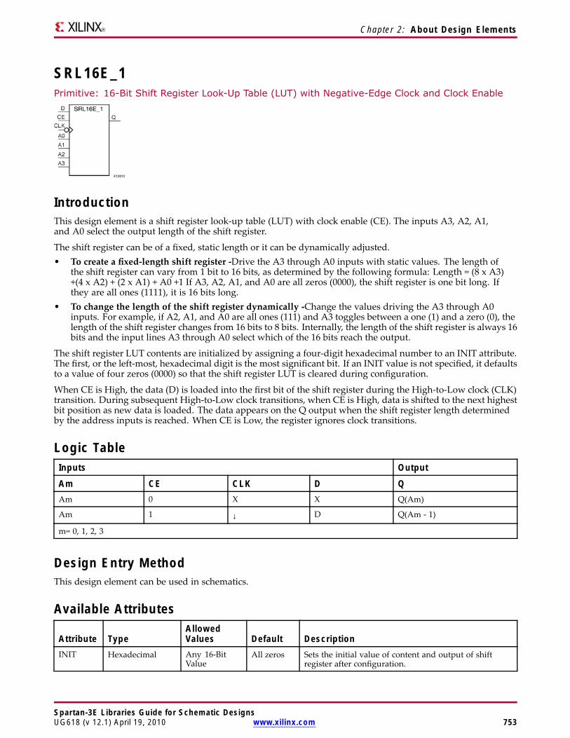
Chapter 2: About Design Elements
SRL16E_1Primitive: 16-Bit Shift Register Look-Up Table (LUT) with Negative-Edge Clock and Clock Enable
IntroductionThis design element is a shift register look-up table (LUT) with clock enable (CE). The inputs A3, A2, A1,and A0 select the output length of the shift register.
The shift register can be of a fixed, static length or it can be dynamically adjusted.• To create a fixed-length shift register -Drive the A3 through A0 inputs with static values. The length of
the shift register can vary from 1 bit to 16 bits, as determined by the following formula: Length = (8 x A3)+(4 x A2) + (2 x A1) + A0 +1 If A3, A2, A1, and A0 are all zeros (0000), the shift register is one bit long. Ifthey are all ones (1111), it is 16 bits long.
• To change the length of the shift register dynamically -Change the values driving the A3 through A0inputs. For example, if A2, A1, and A0 are all ones (111) and A3 toggles between a one (1) and a zero (0), thelength of the shift register changes from 16 bits to 8 bits. Internally, the length of the shift register is always 16bits and the input lines A3 through A0 select which of the 16 bits reach the output.
The shift register LUT contents are initialized by assigning a four-digit hexadecimal number to an INIT attribute.The first, or the left-most, hexadecimal digit is the most significant bit. If an INIT value is not specified, it defaultsto a value of four zeros (0000) so that the shift register LUT is cleared during configuration.
When CE is High, the data (D) is loaded into the first bit of the shift register during the High-to-Low clock (CLK)transition. During subsequent High-to-Low clock transitions, when CE is High, data is shifted to the next highestbit position as new data is loaded. The data appears on the Q output when the shift register length determinedby the address inputs is reached. When CE is Low, the register ignores clock transitions.
Logic TableInputs Output
Am CE CLK D QAm 0 X X Q(Am)
Am 1 ↓ D Q(Am - 1)
m= 0, 1, 2, 3
Design Entry MethodThis design element can be used in schematics.
Available Attributes
Attribute TypeAllowedValues Default Description
INIT Hexadecimal Any 16-BitValue
All zeros Sets the initial value of content and output of shiftregister after configuration.
Spartan-3E Libraries Guide for Schematic DesignsUG618 (v 12.1) April 19, 2010 www.xilinx.com 753

Chapter 2: About Design Elements
For More Information• See the Spartan-3 Generation FPGA User Guide.
• See the Spartan-3E FPGA Family Complete Data Sheet.
Spartan-3E Libraries Guide for Schematic Designs754 www.xilinx.com UG618 (v 12.1) April 19, 2010
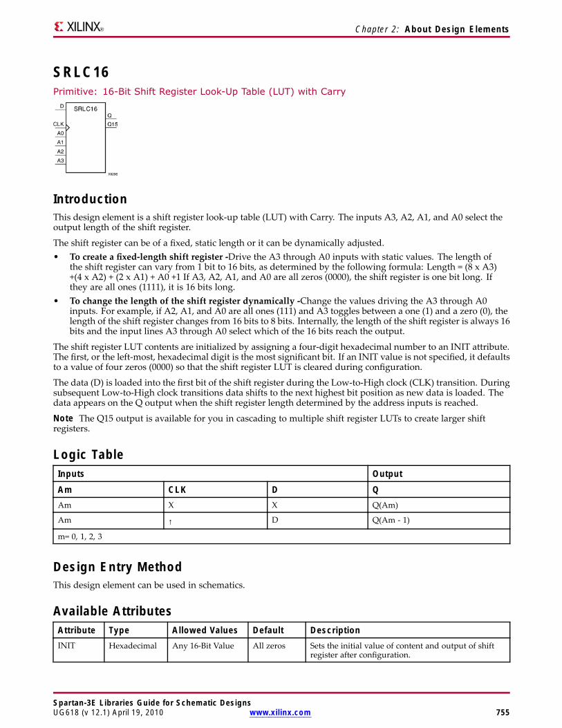
Chapter 2: About Design Elements
SRLC16Primitive: 16-Bit Shift Register Look-Up Table (LUT) with Carry
IntroductionThis design element is a shift register look-up table (LUT) with Carry. The inputs A3, A2, A1, and A0 select theoutput length of the shift register.
The shift register can be of a fixed, static length or it can be dynamically adjusted.• To create a fixed-length shift register -Drive the A3 through A0 inputs with static values. The length of
the shift register can vary from 1 bit to 16 bits, as determined by the following formula: Length = (8 x A3)+(4 x A2) + (2 x A1) + A0 +1 If A3, A2, A1, and A0 are all zeros (0000), the shift register is one bit long. Ifthey are all ones (1111), it is 16 bits long.
• To change the length of the shift register dynamically -Change the values driving the A3 through A0inputs. For example, if A2, A1, and A0 are all ones (111) and A3 toggles between a one (1) and a zero (0), thelength of the shift register changes from 16 bits to 8 bits. Internally, the length of the shift register is always 16bits and the input lines A3 through A0 select which of the 16 bits reach the output.
The shift register LUT contents are initialized by assigning a four-digit hexadecimal number to an INIT attribute.The first, or the left-most, hexadecimal digit is the most significant bit. If an INIT value is not specified, it defaultsto a value of four zeros (0000) so that the shift register LUT is cleared during configuration.
The data (D) is loaded into the first bit of the shift register during the Low-to-High clock (CLK) transition. Duringsubsequent Low-to-High clock transitions data shifts to the next highest bit position as new data is loaded. Thedata appears on the Q output when the shift register length determined by the address inputs is reached.
Note The Q15 output is available for you in cascading to multiple shift register LUTs to create larger shiftregisters.
Logic TableInputs Output
Am CLK D QAm X X Q(Am)
Am ↑ D Q(Am - 1)
m= 0, 1, 2, 3
Design Entry MethodThis design element can be used in schematics.
Available AttributesAttribute Type Allowed Values Default DescriptionINIT Hexadecimal Any 16-Bit Value All zeros Sets the initial value of content and output of shift
register after configuration.
Spartan-3E Libraries Guide for Schematic DesignsUG618 (v 12.1) April 19, 2010 www.xilinx.com 755

Chapter 2: About Design Elements
For More Information• See the Spartan-3 Generation FPGA User Guide.
• See the Spartan-3E FPGA Family Complete Data Sheet.
Spartan-3E Libraries Guide for Schematic Designs756 www.xilinx.com UG618 (v 12.1) April 19, 2010
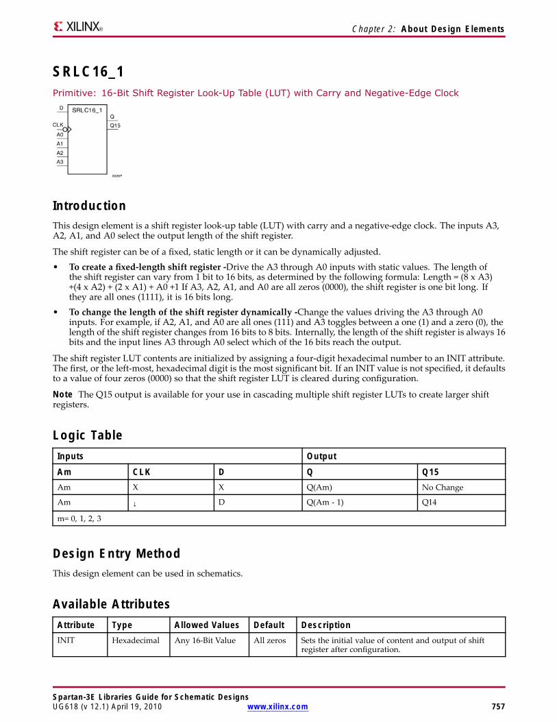
Chapter 2: About Design Elements
SRLC16_1Primitive: 16-Bit Shift Register Look-Up Table (LUT) with Carry and Negative-Edge Clock
IntroductionThis design element is a shift register look-up table (LUT) with carry and a negative-edge clock. The inputs A3,A2, A1, and A0 select the output length of the shift register.
The shift register can be of a fixed, static length or it can be dynamically adjusted.• To create a fixed-length shift register -Drive the A3 through A0 inputs with static values. The length of
the shift register can vary from 1 bit to 16 bits, as determined by the following formula: Length = (8 x A3)+(4 x A2) + (2 x A1) + A0 +1 If A3, A2, A1, and A0 are all zeros (0000), the shift register is one bit long. Ifthey are all ones (1111), it is 16 bits long.
• To change the length of the shift register dynamically -Change the values driving the A3 through A0inputs. For example, if A2, A1, and A0 are all ones (111) and A3 toggles between a one (1) and a zero (0), thelength of the shift register changes from 16 bits to 8 bits. Internally, the length of the shift register is always 16bits and the input lines A3 through A0 select which of the 16 bits reach the output.
The shift register LUT contents are initialized by assigning a four-digit hexadecimal number to an INIT attribute.The first, or the left-most, hexadecimal digit is the most significant bit. If an INIT value is not specified, it defaultsto a value of four zeros (0000) so that the shift register LUT is cleared during configuration.
Note The Q15 output is available for your use in cascading multiple shift register LUTs to create larger shiftregisters.
Logic TableInputs Output
Am CLK D Q Q15Am X X Q(Am) No Change
Am ↓ D Q(Am - 1) Q14
m= 0, 1, 2, 3
Design Entry MethodThis design element can be used in schematics.
Available AttributesAttribute Type Allowed Values Default DescriptionINIT Hexadecimal Any 16-Bit Value All zeros Sets the initial value of content and output of shift
register after configuration.
Spartan-3E Libraries Guide for Schematic DesignsUG618 (v 12.1) April 19, 2010 www.xilinx.com 757

Chapter 2: About Design Elements
For More Information• See the Spartan-3 Generation FPGA User Guide.
• See the Spartan-3E FPGA Family Complete Data Sheet.
Spartan-3E Libraries Guide for Schematic Designs758 www.xilinx.com UG618 (v 12.1) April 19, 2010
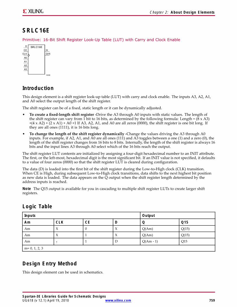
Chapter 2: About Design Elements
SRLC16EPrimitive: 16-Bit Shift Register Look-Up Table (LUT) with Carry and Clock Enable
IntroductionThis design element is a shift register look-up table (LUT) with carry and clock enable. The inputs A3, A2, A1,and A0 select the output length of the shift register.
The shift register can be of a fixed, static length or it can be dynamically adjusted.
• To create a fixed-length shift register -Drive the A3 through A0 inputs with static values. The length ofthe shift register can vary from 1 bit to 16 bits, as determined by the following formula: Length = (8 x A3)+(4 x A2) + (2 x A1) + A0 +1 If A3, A2, A1, and A0 are all zeros (0000), the shift register is one bit long. Ifthey are all ones (1111), it is 16 bits long.
• To change the length of the shift register dynamically -Change the values driving the A3 through A0inputs. For example, if A2, A1, and A0 are all ones (111) and A3 toggles between a one (1) and a zero (0), thelength of the shift register changes from 16 bits to 8 bits. Internally, the length of the shift register is always 16bits and the input lines A3 through A0 select which of the 16 bits reach the output.
The shift register LUT contents are initialized by assigning a four-digit hexadecimal number to an INIT attribute.The first, or the left-most, hexadecimal digit is the most significant bit. If an INIT value is not specified, it defaultsto a value of four zeros (0000) so that the shift register LUT is cleared during configuration.
The data (D) is loaded into the first bit of the shift register during the Low-to-High clock (CLK) transition.When CE is High, during subsequent Low-to-High clock transitions, data shifts to the next highest bit positionas new data is loaded. The data appears on the Q output when the shift register length determined by theaddress inputs is reached.
Note The Q15 output is available for you in cascading to multiple shift register LUTs to create larger shiftregisters.
Logic TableInputs Output
Am CLK CE D Q Q15Am X 0 X Q(Am) Q(15)
Am X 1 X Q(Am) Q(15)
Am ↑ 1 D Q(Am - 1) Q15
m= 0, 1, 2, 3
Design Entry MethodThis design element can be used in schematics.
Spartan-3E Libraries Guide for Schematic DesignsUG618 (v 12.1) April 19, 2010 www.xilinx.com 759
Chapter 2: About Design Elements
Available AttributesAttribute Type Allowed Values Default DescriptionINIT Hexadecimal Any 16-Bit Value All zeros Sets the initial value of content and output of shift
register after configuration.
For More Information• See the Spartan-3 Generation FPGA User Guide.
• See the Spartan-3E FPGA Family Complete Data Sheet.
Spartan-3E Libraries Guide for Schematic Designs760 www.xilinx.com UG618 (v 12.1) April 19, 2010
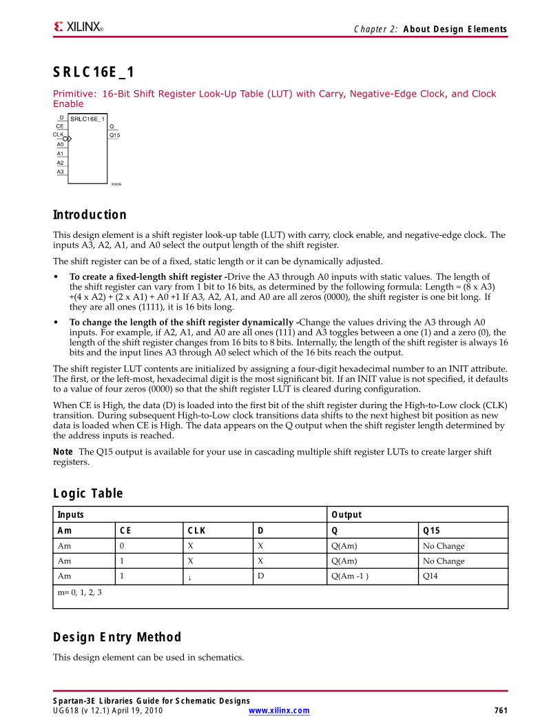
Chapter 2: About Design Elements
SRLC16E_1Primitive: 16-Bit Shift Register Look-Up Table (LUT) with Carry, Negative-Edge Clock, and ClockEnable
IntroductionThis design element is a shift register look-up table (LUT) with carry, clock enable, and negative-edge clock. Theinputs A3, A2, A1, and A0 select the output length of the shift register.
The shift register can be of a fixed, static length or it can be dynamically adjusted.
• To create a fixed-length shift register -Drive the A3 through A0 inputs with static values. The length ofthe shift register can vary from 1 bit to 16 bits, as determined by the following formula: Length = (8 x A3)+(4 x A2) + (2 x A1) + A0 +1 If A3, A2, A1, and A0 are all zeros (0000), the shift register is one bit long. Ifthey are all ones (1111), it is 16 bits long.
• To change the length of the shift register dynamically -Change the values driving the A3 through A0inputs. For example, if A2, A1, and A0 are all ones (111) and A3 toggles between a one (1) and a zero (0), thelength of the shift register changes from 16 bits to 8 bits. Internally, the length of the shift register is always 16bits and the input lines A3 through A0 select which of the 16 bits reach the output.
The shift register LUT contents are initialized by assigning a four-digit hexadecimal number to an INIT attribute.The first, or the left-most, hexadecimal digit is the most significant bit. If an INIT value is not specified, it defaultsto a value of four zeros (0000) so that the shift register LUT is cleared during configuration.
When CE is High, the data (D) is loaded into the first bit of the shift register during the High-to-Low clock (CLK)transition. During subsequent High-to-Low clock transitions data shifts to the next highest bit position as newdata is loaded when CE is High. The data appears on the Q output when the shift register length determined bythe address inputs is reached.
Note The Q15 output is available for your use in cascading multiple shift register LUTs to create larger shiftregisters.
Logic TableInputs Output
Am CE CLK D Q Q15Am 0 X X Q(Am) No Change
Am 1 X X Q(Am) No Change
Am 1 ↓ D Q(Am -1 ) Q14
m= 0, 1, 2, 3
Design Entry MethodThis design element can be used in schematics.
Spartan-3E Libraries Guide for Schematic DesignsUG618 (v 12.1) April 19, 2010 www.xilinx.com 761
Chapter 2: About Design Elements
Available Attributes
Attribute TypeAllowedValues Default Description
INIT Hexadecimal Any 16-BitValue
All zeros Sets the initial value of content and output of shift registerafter configuration.
For More Information• See the Spartan-3 Generation FPGA User Guide.
• See the Spartan-3E FPGA Family Complete Data Sheet.
Spartan-3E Libraries Guide for Schematic Designs762 www.xilinx.com UG618 (v 12.1) April 19, 2010
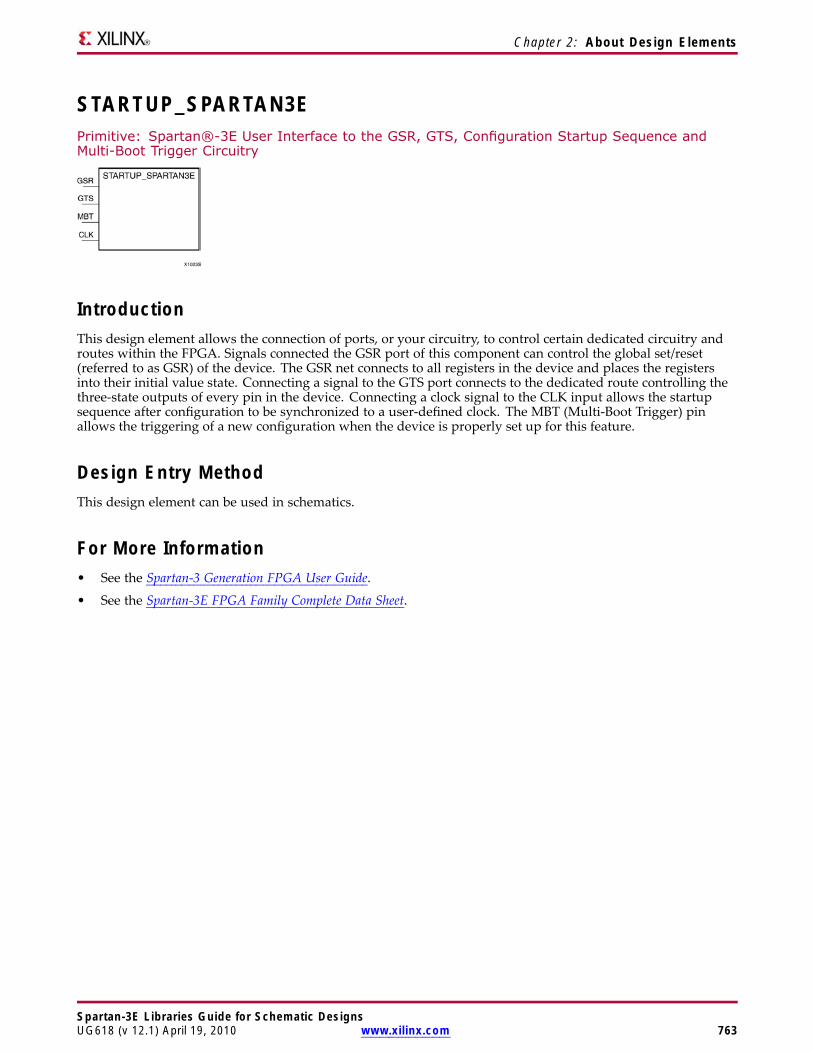
Chapter 2: About Design Elements
STARTUP_SPARTAN3EPrimitive: Spartan®-3E User Interface to the GSR, GTS, Configuration Startup Sequence andMulti-Boot Trigger Circuitry
IntroductionThis design element allows the connection of ports, or your circuitry, to control certain dedicated circuitry androutes within the FPGA. Signals connected the GSR port of this component can control the global set/reset(referred to as GSR) of the device. The GSR net connects to all registers in the device and places the registersinto their initial value state. Connecting a signal to the GTS port connects to the dedicated route controlling thethree-state outputs of every pin in the device. Connecting a clock signal to the CLK input allows the startupsequence after configuration to be synchronized to a user-defined clock. The MBT (Multi-Boot Trigger) pinallows the triggering of a new configuration when the device is properly set up for this feature.
Design Entry MethodThis design element can be used in schematics.
For More Information• See the Spartan-3 Generation FPGA User Guide.
• See the Spartan-3E FPGA Family Complete Data Sheet.
Spartan-3E Libraries Guide for Schematic DesignsUG618 (v 12.1) April 19, 2010 www.xilinx.com 763

Chapter 2: About Design Elements
VCCPrimitive: VCC-Connection Signal Tag
IntroductionThis design element serves as a signal tag, or parameter, that forces a net or input function to a logic High level.A net tied to this element cannot have any other source.
When the placement and routing software encounters a net or input function tied to this element, it removes anylogic that is disabled by the Vcc signal, which is only implemented when the disabled logic cannot be removed.
Design Entry MethodThis design element is only for use in schematics.
For More Information• See the Spartan-3 Generation FPGA User Guide.
• See the Spartan-3E FPGA Family Complete Data Sheet.
Spartan-3E Libraries Guide for Schematic Designs764 www.xilinx.com UG618 (v 12.1) April 19, 2010
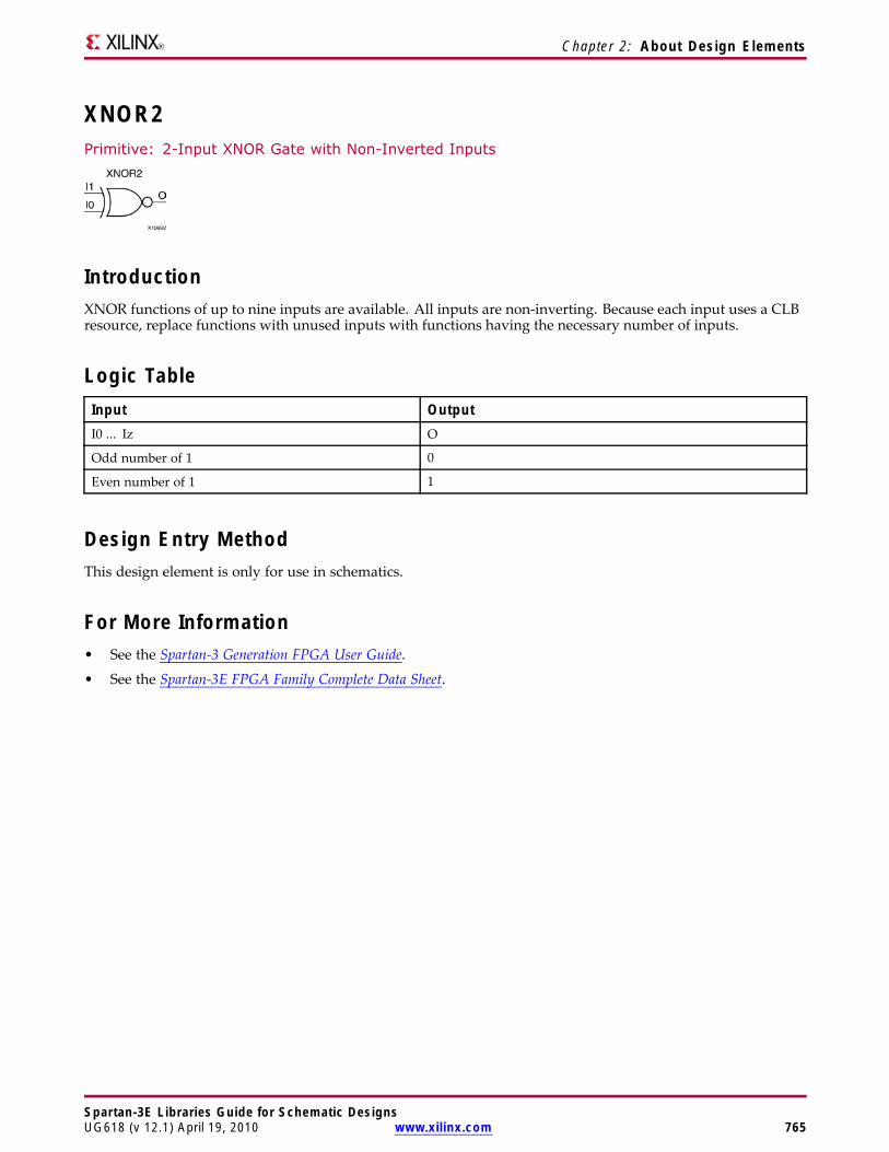
Chapter 2: About Design Elements
XNOR2Primitive: 2-Input XNOR Gate with Non-Inverted Inputs
IntroductionXNOR functions of up to nine inputs are available. All inputs are non-inverting. Because each input uses a CLBresource, replace functions with unused inputs with functions having the necessary number of inputs.
Logic TableInput OutputI0 ... Iz O
Odd number of 1 0
Even number of 1 1
Design Entry MethodThis design element is only for use in schematics.
For More Information• See the Spartan-3 Generation FPGA User Guide.
• See the Spartan-3E FPGA Family Complete Data Sheet.
Spartan-3E Libraries Guide for Schematic DesignsUG618 (v 12.1) April 19, 2010 www.xilinx.com 765
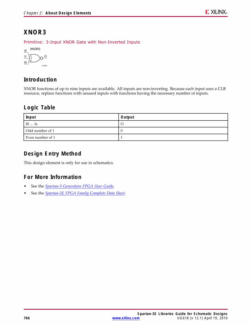
Chapter 2: About Design Elements
XNOR3Primitive: 3-Input XNOR Gate with Non-Inverted Inputs
IntroductionXNOR functions of up to nine inputs are available. All inputs are non-inverting. Because each input uses a CLBresource, replace functions with unused inputs with functions having the necessary number of inputs.
Logic TableInput OutputI0 ... Iz O
Odd number of 1 0
Even number of 1 1
Design Entry MethodThis design element is only for use in schematics.
For More Information• See the Spartan-3 Generation FPGA User Guide.
• See the Spartan-3E FPGA Family Complete Data Sheet.
Spartan-3E Libraries Guide for Schematic Designs766 www.xilinx.com UG618 (v 12.1) April 19, 2010
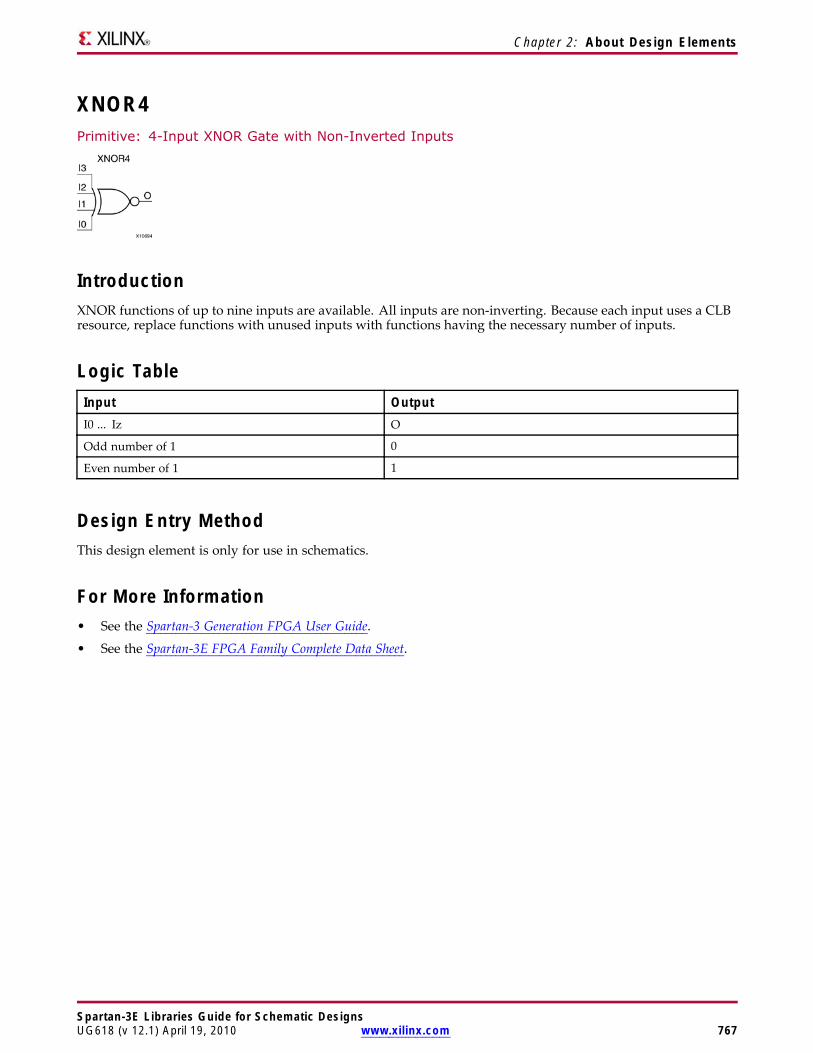
Chapter 2: About Design Elements
XNOR4Primitive: 4-Input XNOR Gate with Non-Inverted Inputs
IntroductionXNOR functions of up to nine inputs are available. All inputs are non-inverting. Because each input uses a CLBresource, replace functions with unused inputs with functions having the necessary number of inputs.
Logic TableInput OutputI0 ... Iz O
Odd number of 1 0
Even number of 1 1
Design Entry MethodThis design element is only for use in schematics.
For More Information• See the Spartan-3 Generation FPGA User Guide.
• See the Spartan-3E FPGA Family Complete Data Sheet.
Spartan-3E Libraries Guide for Schematic DesignsUG618 (v 12.1) April 19, 2010 www.xilinx.com 767
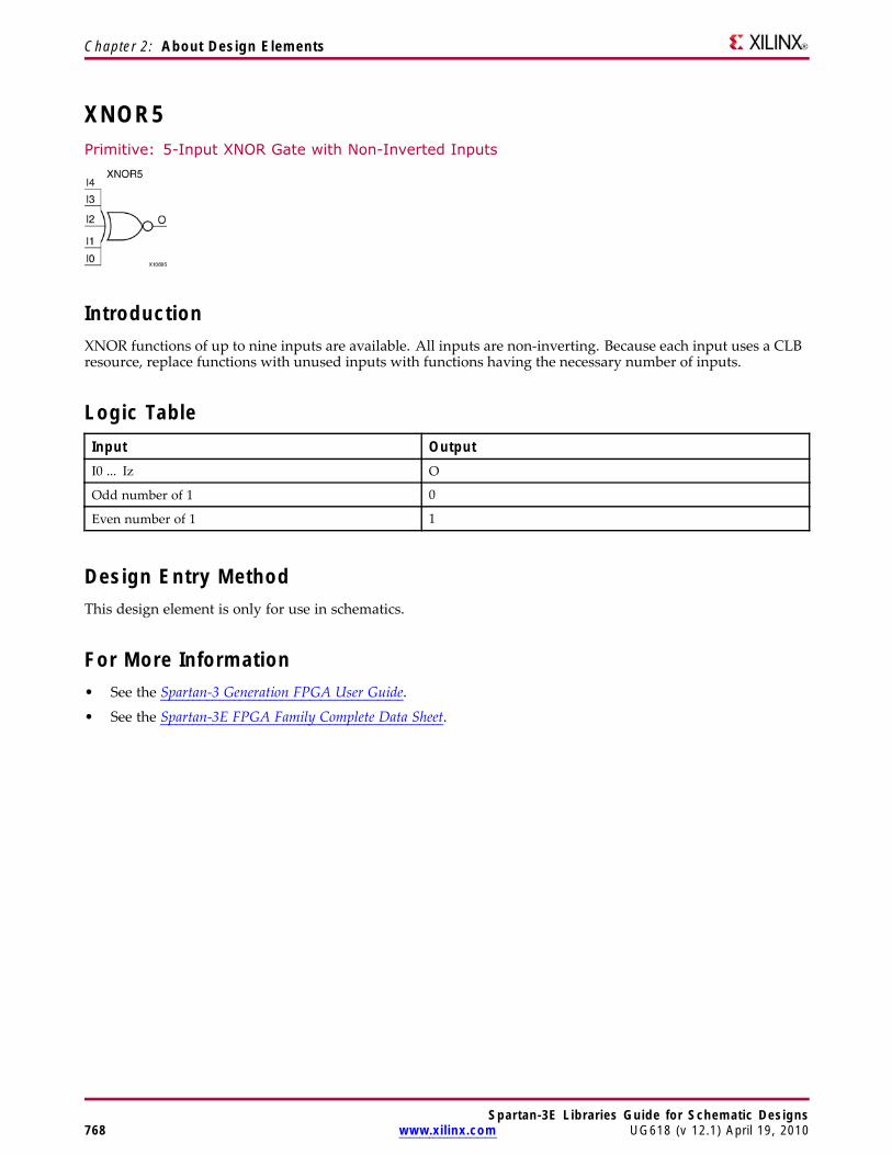
Chapter 2: About Design Elements
XNOR5Primitive: 5-Input XNOR Gate with Non-Inverted Inputs
IntroductionXNOR functions of up to nine inputs are available. All inputs are non-inverting. Because each input uses a CLBresource, replace functions with unused inputs with functions having the necessary number of inputs.
Logic TableInput OutputI0 ... Iz O
Odd number of 1 0
Even number of 1 1
Design Entry MethodThis design element is only for use in schematics.
For More Information• See the Spartan-3 Generation FPGA User Guide.
• See the Spartan-3E FPGA Family Complete Data Sheet.
Spartan-3E Libraries Guide for Schematic Designs768 www.xilinx.com UG618 (v 12.1) April 19, 2010
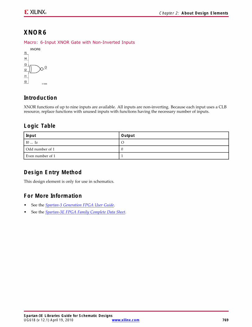
Chapter 2: About Design Elements
XNOR6Macro: 6-Input XNOR Gate with Non-Inverted Inputs
IntroductionXNOR functions of up to nine inputs are available. All inputs are non-inverting. Because each input uses a CLBresource, replace functions with unused inputs with functions having the necessary number of inputs.
Logic TableInput OutputI0 ... Iz O
Odd number of 1 0
Even number of 1 1
Design Entry MethodThis design element is only for use in schematics.
For More Information• See the Spartan-3 Generation FPGA User Guide.
• See the Spartan-3E FPGA Family Complete Data Sheet.
Spartan-3E Libraries Guide for Schematic DesignsUG618 (v 12.1) April 19, 2010 www.xilinx.com 769
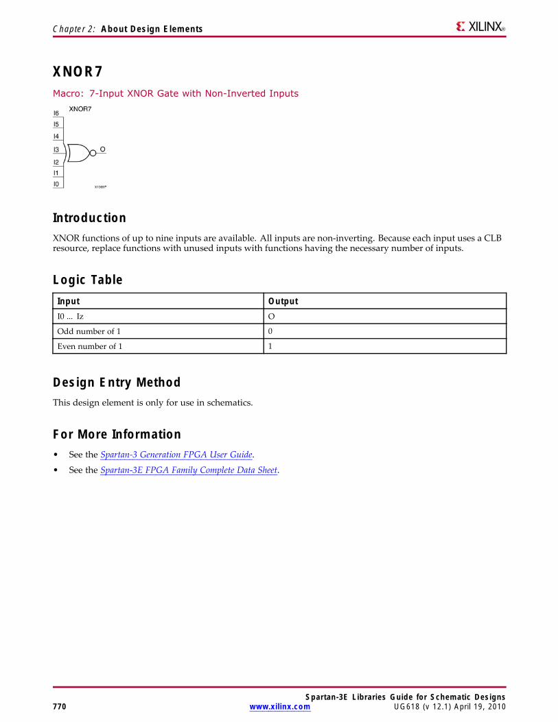
Chapter 2: About Design Elements
XNOR7Macro: 7-Input XNOR Gate with Non-Inverted Inputs
IntroductionXNOR functions of up to nine inputs are available. All inputs are non-inverting. Because each input uses a CLBresource, replace functions with unused inputs with functions having the necessary number of inputs.
Logic TableInput OutputI0 ... Iz O
Odd number of 1 0
Even number of 1 1
Design Entry MethodThis design element is only for use in schematics.
For More Information• See the Spartan-3 Generation FPGA User Guide.
• See the Spartan-3E FPGA Family Complete Data Sheet.
Spartan-3E Libraries Guide for Schematic Designs770 www.xilinx.com UG618 (v 12.1) April 19, 2010
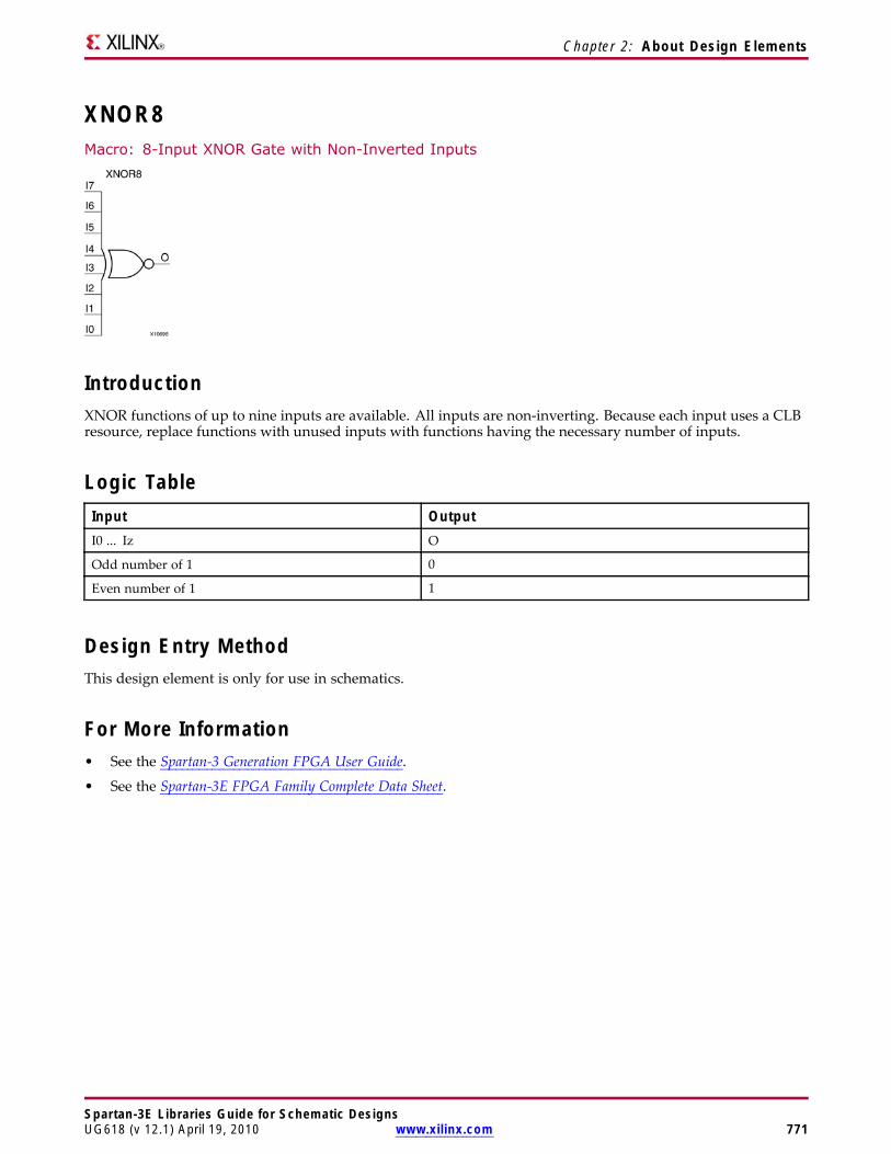
Chapter 2: About Design Elements
XNOR8Macro: 8-Input XNOR Gate with Non-Inverted Inputs
IntroductionXNOR functions of up to nine inputs are available. All inputs are non-inverting. Because each input uses a CLBresource, replace functions with unused inputs with functions having the necessary number of inputs.
Logic TableInput OutputI0 ... Iz O
Odd number of 1 0
Even number of 1 1
Design Entry MethodThis design element is only for use in schematics.
For More Information• See the Spartan-3 Generation FPGA User Guide.
• See the Spartan-3E FPGA Family Complete Data Sheet.
Spartan-3E Libraries Guide for Schematic DesignsUG618 (v 12.1) April 19, 2010 www.xilinx.com 771
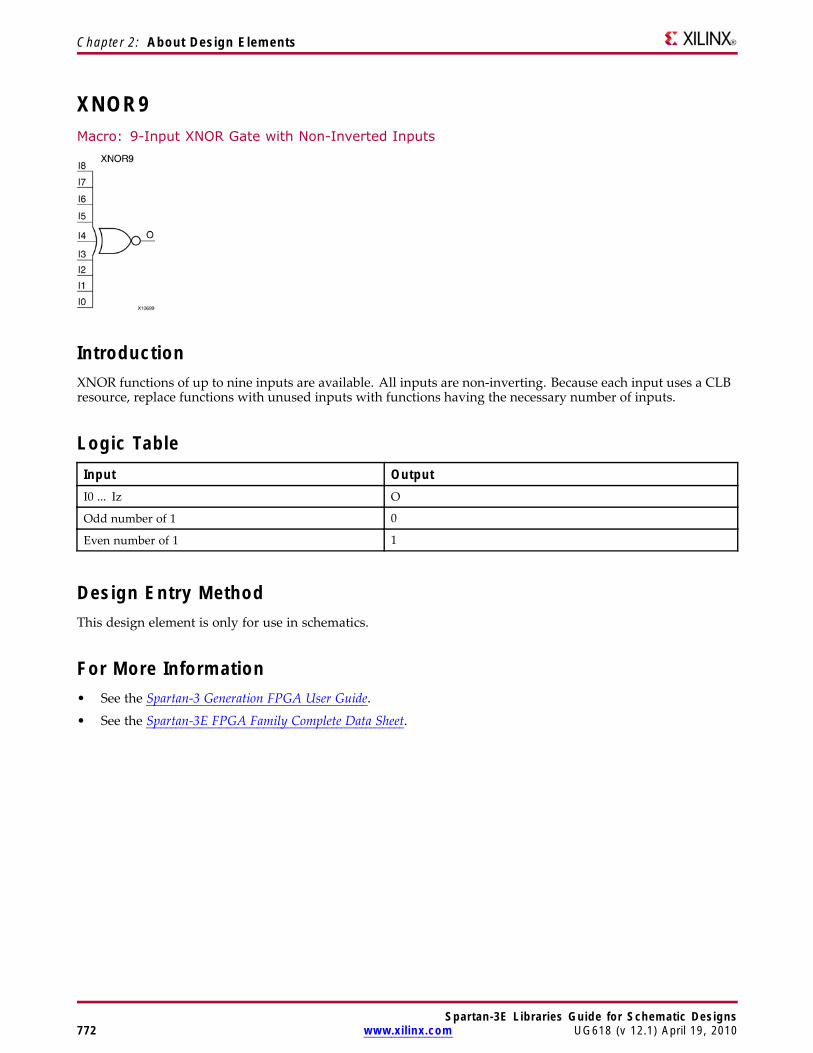
Chapter 2: About Design Elements
XNOR9Macro: 9-Input XNOR Gate with Non-Inverted Inputs
IntroductionXNOR functions of up to nine inputs are available. All inputs are non-inverting. Because each input uses a CLBresource, replace functions with unused inputs with functions having the necessary number of inputs.
Logic TableInput OutputI0 ... Iz O
Odd number of 1 0
Even number of 1 1
Design Entry MethodThis design element is only for use in schematics.
For More Information• See the Spartan-3 Generation FPGA User Guide.
• See the Spartan-3E FPGA Family Complete Data Sheet.
Spartan-3E Libraries Guide for Schematic Designs772 www.xilinx.com UG618 (v 12.1) April 19, 2010
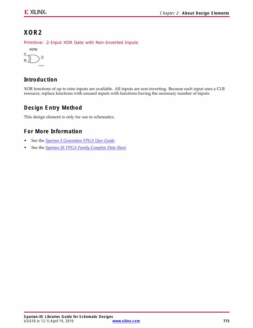
Chapter 2: About Design Elements
XOR2Primitive: 2-Input XOR Gate with Non-Inverted Inputs
IntroductionXOR functions of up to nine inputs are available. All inputs are non-inverting. Because each input uses a CLBresource, replace functions with unused inputs with functions having the necessary number of inputs.
Design Entry MethodThis design element is only for use in schematics.
For More Information• See the Spartan-3 Generation FPGA User Guide.
• See the Spartan-3E FPGA Family Complete Data Sheet.
Spartan-3E Libraries Guide for Schematic DesignsUG618 (v 12.1) April 19, 2010 www.xilinx.com 773

Chapter 2: About Design Elements
XOR3Primitive: 3-Input XOR Gate with Non-Inverted Inputs
IntroductionXOR functions of up to nine inputs are available. All inputs are non-inverting. Because each input uses a CLBresource, replace functions with unused inputs with functions having the necessary number of inputs.
Design Entry MethodThis design element is only for use in schematics.
For More Information• See the Spartan-3 Generation FPGA User Guide.
• See the Spartan-3E FPGA Family Complete Data Sheet.
Spartan-3E Libraries Guide for Schematic Designs774 www.xilinx.com UG618 (v 12.1) April 19, 2010
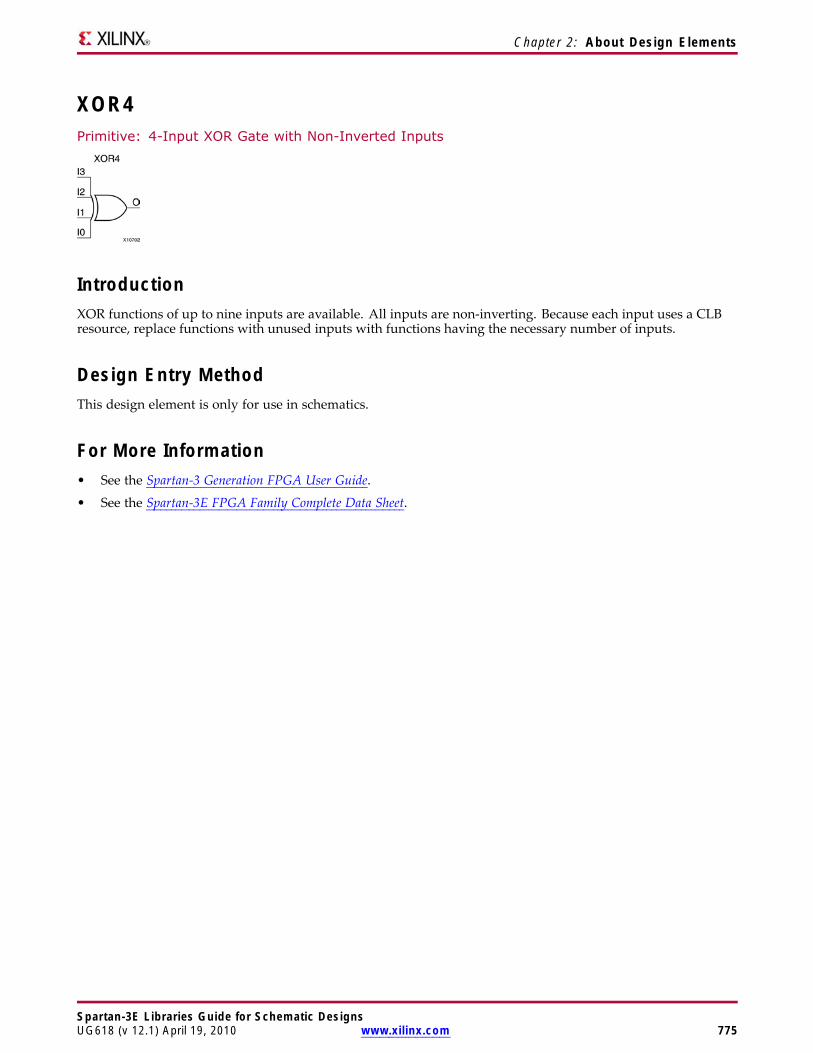
Chapter 2: About Design Elements
XOR4Primitive: 4-Input XOR Gate with Non-Inverted Inputs
IntroductionXOR functions of up to nine inputs are available. All inputs are non-inverting. Because each input uses a CLBresource, replace functions with unused inputs with functions having the necessary number of inputs.
Design Entry MethodThis design element is only for use in schematics.
For More Information• See the Spartan-3 Generation FPGA User Guide.
• See the Spartan-3E FPGA Family Complete Data Sheet.
Spartan-3E Libraries Guide for Schematic DesignsUG618 (v 12.1) April 19, 2010 www.xilinx.com 775
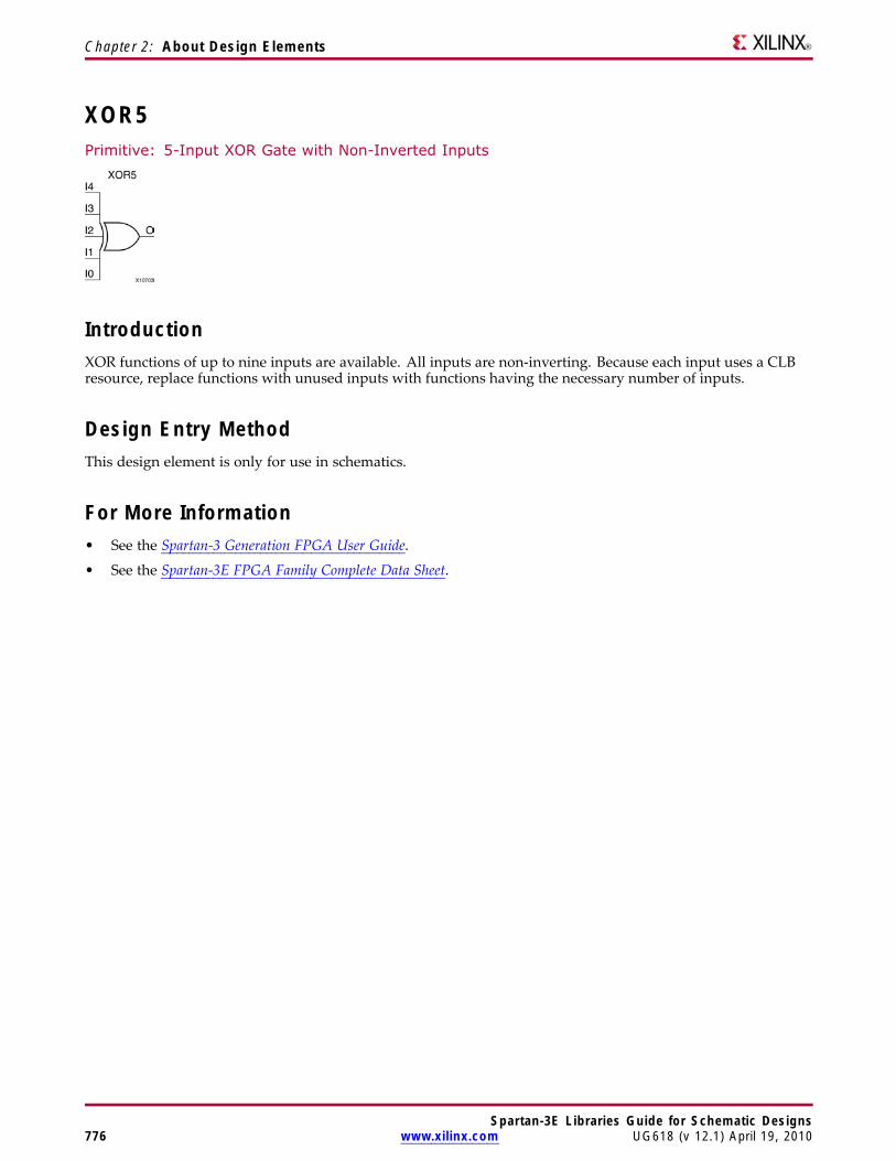
Chapter 2: About Design Elements
XOR5Primitive: 5-Input XOR Gate with Non-Inverted Inputs
IntroductionXOR functions of up to nine inputs are available. All inputs are non-inverting. Because each input uses a CLBresource, replace functions with unused inputs with functions having the necessary number of inputs.
Design Entry MethodThis design element is only for use in schematics.
For More Information• See the Spartan-3 Generation FPGA User Guide.
• See the Spartan-3E FPGA Family Complete Data Sheet.
Spartan-3E Libraries Guide for Schematic Designs776 www.xilinx.com UG618 (v 12.1) April 19, 2010

Chapter 2: About Design Elements
XOR6Macro: 6-Input XOR Gate with Non-Inverted Inputs
IntroductionXOR functions of up to nine inputs are available. All inputs are non-inverting. Because each input uses a CLBresource, replace functions with unused inputs with functions having the necessary number of inputs.
Design Entry MethodThis design element is only for use in schematics.
For More Information• See the Spartan-3 Generation FPGA User Guide.
• See the Spartan-3E FPGA Family Complete Data Sheet.
Spartan-3E Libraries Guide for Schematic DesignsUG618 (v 12.1) April 19, 2010 www.xilinx.com 777
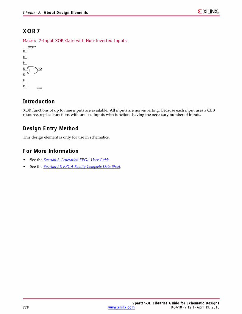
Chapter 2: About Design Elements
XOR7Macro: 7-Input XOR Gate with Non-Inverted Inputs
IntroductionXOR functions of up to nine inputs are available. All inputs are non-inverting. Because each input uses a CLBresource, replace functions with unused inputs with functions having the necessary number of inputs.
Design Entry MethodThis design element is only for use in schematics.
For More Information• See the Spartan-3 Generation FPGA User Guide.
• See the Spartan-3E FPGA Family Complete Data Sheet.
Spartan-3E Libraries Guide for Schematic Designs778 www.xilinx.com UG618 (v 12.1) April 19, 2010
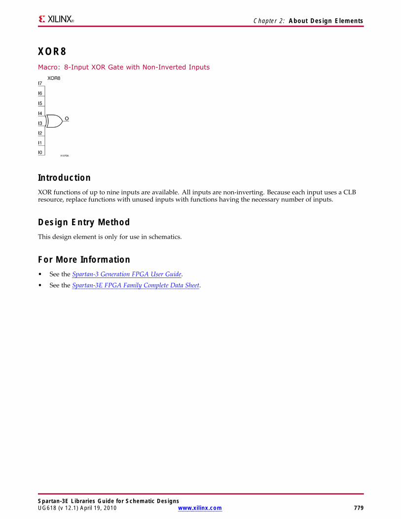
Chapter 2: About Design Elements
XOR8Macro: 8-Input XOR Gate with Non-Inverted Inputs
IntroductionXOR functions of up to nine inputs are available. All inputs are non-inverting. Because each input uses a CLBresource, replace functions with unused inputs with functions having the necessary number of inputs.
Design Entry MethodThis design element is only for use in schematics.
For More Information• See the Spartan-3 Generation FPGA User Guide.
• See the Spartan-3E FPGA Family Complete Data Sheet.
Spartan-3E Libraries Guide for Schematic DesignsUG618 (v 12.1) April 19, 2010 www.xilinx.com 779
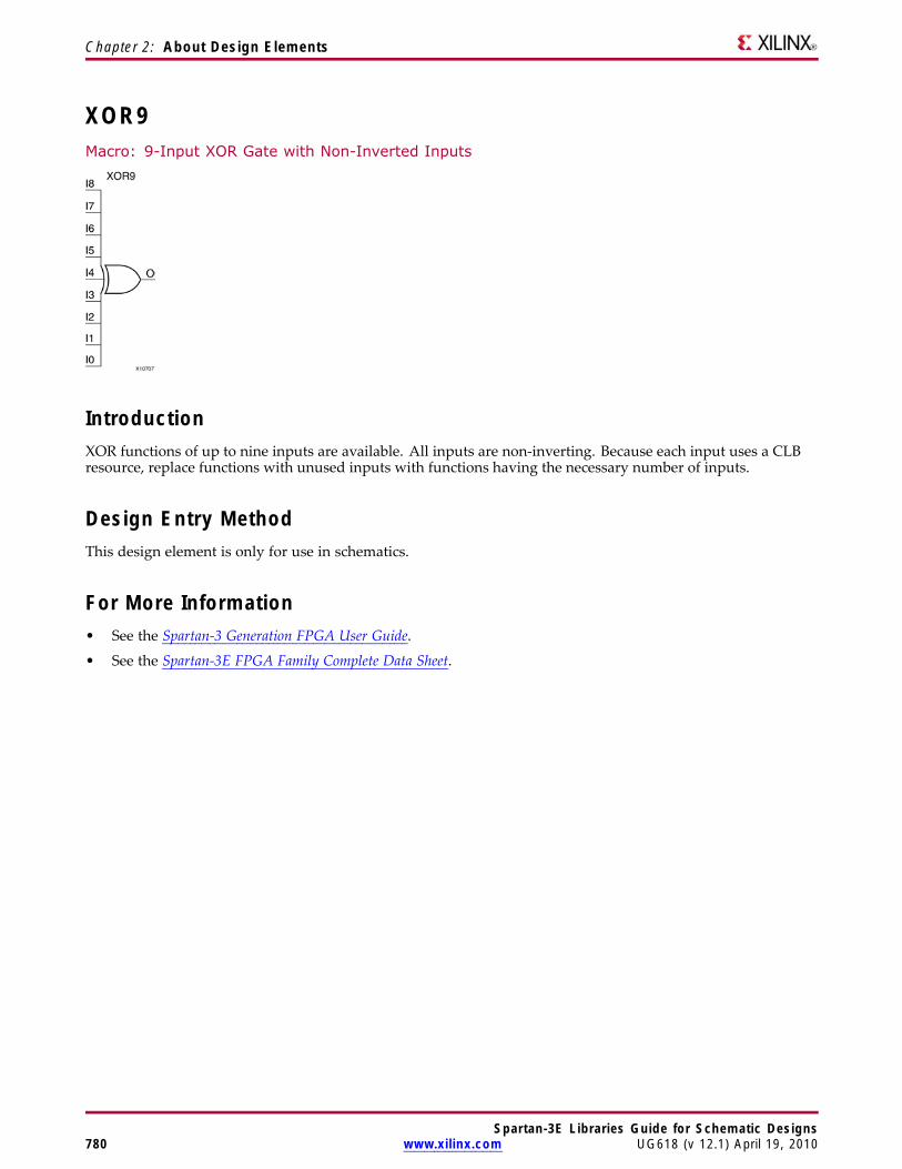
Chapter 2: About Design Elements
XOR9Macro: 9-Input XOR Gate with Non-Inverted Inputs
IntroductionXOR functions of up to nine inputs are available. All inputs are non-inverting. Because each input uses a CLBresource, replace functions with unused inputs with functions having the necessary number of inputs.
Design Entry MethodThis design element is only for use in schematics.
For More Information• See the Spartan-3 Generation FPGA User Guide.
• See the Spartan-3E FPGA Family Complete Data Sheet.
Spartan-3E Libraries Guide for Schematic Designs780 www.xilinx.com UG618 (v 12.1) April 19, 2010
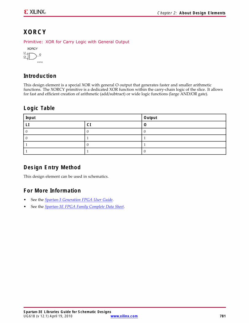
Chapter 2: About Design Elements
XORCYPrimitive: XOR for Carry Logic with General Output
IntroductionThis design element is a special XOR with general O output that generates faster and smaller arithmeticfunctions. The XORCY primitive is a dedicated XOR function within the carry-chain logic of the slice. It allowsfor fast and efficient creation of arithmetic (add/subtract) or wide logic functions (large AND/OR gate).
Logic TableInput Output
LI CI O0 0 0
0 1 1
1 0 1
1 1 0
Design Entry MethodThis design element can be used in schematics.
For More Information• See the Spartan-3 Generation FPGA User Guide.
• See the Spartan-3E FPGA Family Complete Data Sheet.
Spartan-3E Libraries Guide for Schematic DesignsUG618 (v 12.1) April 19, 2010 www.xilinx.com 781
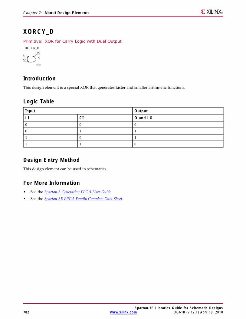
Chapter 2: About Design Elements
XORCY_DPrimitive: XOR for Carry Logic with Dual Output
IntroductionThis design element is a special XOR that generates faster and smaller arithmetic functions.
Logic TableInput Output
LI CI O and LO0 0 0
0 1 1
1 0 1
1 1 0
Design Entry MethodThis design element can be used in schematics.
For More Information• See the Spartan-3 Generation FPGA User Guide.
• See the Spartan-3E FPGA Family Complete Data Sheet.
Spartan-3E Libraries Guide for Schematic Designs782 www.xilinx.com UG618 (v 12.1) April 19, 2010
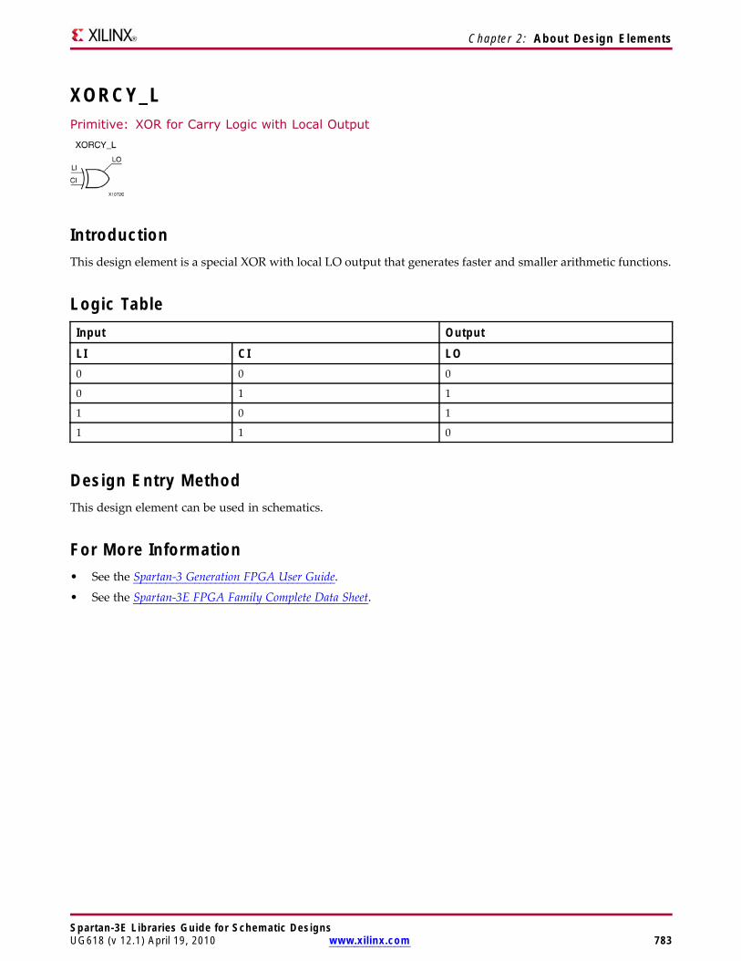
Chapter 2: About Design Elements
XORCY_LPrimitive: XOR for Carry Logic with Local Output
IntroductionThis design element is a special XOR with local LO output that generates faster and smaller arithmetic functions.
Logic TableInput Output
LI CI LO0 0 0
0 1 1
1 0 1
1 1 0
Design Entry MethodThis design element can be used in schematics.
For More Information• See the Spartan-3 Generation FPGA User Guide.
• See the Spartan-3E FPGA Family Complete Data Sheet.
Spartan-3E Libraries Guide for Schematic DesignsUG618 (v 12.1) April 19, 2010 www.xilinx.com 783