
Xilinx PG150 LogiCORE IP UltraScale Architecture … · LogiCORE IP UltraScale Architecture-Based...
158
LogiCORE IP UltraScale Architecture-Based FPGAs Memory Interface Solutions v5.0 Product Guide Vivado Design Suite PG150 June 4, 2014
Transcript of Xilinx PG150 LogiCORE IP UltraScale Architecture … · LogiCORE IP UltraScale Architecture-Based...
LogiCORE IP UltraScale Architecture-Based FPGAs Memory Interface Solutions v5.0
Product GuideVivado Design Suite
PG150 June 4, 2014
UltraScale Architecture-Based FPGAs MIS www.xilinx.com 2PG150 June 4, 2014
Table of Contents
SECTION I: SUMMARY
IP Facts
SECTION II: DDR3/DDR4
Chapter 1: OverviewFeature Summary. . . . . . . . . . . . . . . . . . . . . . . . . . . . . . . . . . . . . . . . . . . . . . . . . . . . . . . . . . . . . . . . . 11Licensing and Ordering Information . . . . . . . . . . . . . . . . . . . . . . . . . . . . . . . . . . . . . . . . . . . . . . . . . . 12
Chapter 2: Product SpecificationStandards . . . . . . . . . . . . . . . . . . . . . . . . . . . . . . . . . . . . . . . . . . . . . . . . . . . . . . . . . . . . . . . . . . . . . . . 13Performance. . . . . . . . . . . . . . . . . . . . . . . . . . . . . . . . . . . . . . . . . . . . . . . . . . . . . . . . . . . . . . . . . . . . . 13Resource Utilization. . . . . . . . . . . . . . . . . . . . . . . . . . . . . . . . . . . . . . . . . . . . . . . . . . . . . . . . . . . . . . . 13Port Descriptions . . . . . . . . . . . . . . . . . . . . . . . . . . . . . . . . . . . . . . . . . . . . . . . . . . . . . . . . . . . . . . . . . 14
Chapter 3: Core ArchitectureOverview . . . . . . . . . . . . . . . . . . . . . . . . . . . . . . . . . . . . . . . . . . . . . . . . . . . . . . . . . . . . . . . . . . . . . . . 15Memory Controller . . . . . . . . . . . . . . . . . . . . . . . . . . . . . . . . . . . . . . . . . . . . . . . . . . . . . . . . . . . . . . . 16PHY . . . . . . . . . . . . . . . . . . . . . . . . . . . . . . . . . . . . . . . . . . . . . . . . . . . . . . . . . . . . . . . . . . . . . . . . . . . . 19
Chapter 4: Designing with the CoreClocking. . . . . . . . . . . . . . . . . . . . . . . . . . . . . . . . . . . . . . . . . . . . . . . . . . . . . . . . . . . . . . . . . . . . . . . . . 26Resets . . . . . . . . . . . . . . . . . . . . . . . . . . . . . . . . . . . . . . . . . . . . . . . . . . . . . . . . . . . . . . . . . . . . . . . . . . 28PCB Guidelines for DDR3 . . . . . . . . . . . . . . . . . . . . . . . . . . . . . . . . . . . . . . . . . . . . . . . . . . . . . . . . . . . 29PCB Guidelines for DDR4 . . . . . . . . . . . . . . . . . . . . . . . . . . . . . . . . . . . . . . . . . . . . . . . . . . . . . . . . . . . 29Pin and Bank Rules. . . . . . . . . . . . . . . . . . . . . . . . . . . . . . . . . . . . . . . . . . . . . . . . . . . . . . . . . . . . . . . . 29Protocol Description . . . . . . . . . . . . . . . . . . . . . . . . . . . . . . . . . . . . . . . . . . . . . . . . . . . . . . . . . . . . . . 38
Chapter 5: Design Flow StepsCustomizing and Generating the Core . . . . . . . . . . . . . . . . . . . . . . . . . . . . . . . . . . . . . . . . . . . . . . . . 55
Send Feedback
UltraScale Architecture-Based FPGAs MIS www.xilinx.com 3PG150 June 4, 2014
Constraining the Core . . . . . . . . . . . . . . . . . . . . . . . . . . . . . . . . . . . . . . . . . . . . . . . . . . . . . . . . . . . . . 65Simulation . . . . . . . . . . . . . . . . . . . . . . . . . . . . . . . . . . . . . . . . . . . . . . . . . . . . . . . . . . . . . . . . . . . . . . 66Synthesis and Implementation . . . . . . . . . . . . . . . . . . . . . . . . . . . . . . . . . . . . . . . . . . . . . . . . . . . . . . 67
Chapter 6: Example DesignSimulating the Example Design (Designs with Standard User Interface). . . . . . . . . . . . . . . . . . . . . 69Synplify Pro Black Box Testing . . . . . . . . . . . . . . . . . . . . . . . . . . . . . . . . . . . . . . . . . . . . . . . . . . . . . . 70
Chapter 7: Test BenchStimulus Pattern . . . . . . . . . . . . . . . . . . . . . . . . . . . . . . . . . . . . . . . . . . . . . . . . . . . . . . . . . . . . . . . . . 73Bus Utilization . . . . . . . . . . . . . . . . . . . . . . . . . . . . . . . . . . . . . . . . . . . . . . . . . . . . . . . . . . . . . . . . . . . 74Example Patterns . . . . . . . . . . . . . . . . . . . . . . . . . . . . . . . . . . . . . . . . . . . . . . . . . . . . . . . . . . . . . . . . . 75Simulating the Performance Traffic Generator . . . . . . . . . . . . . . . . . . . . . . . . . . . . . . . . . . . . . . . . . 78
SECTION III: QDR II+ SRAM
Chapter 8: OverviewFeature Summary. . . . . . . . . . . . . . . . . . . . . . . . . . . . . . . . . . . . . . . . . . . . . . . . . . . . . . . . . . . . . . . . . 82Licensing and Ordering Information . . . . . . . . . . . . . . . . . . . . . . . . . . . . . . . . . . . . . . . . . . . . . . . . . . 82
Chapter 9: Product SpecificationStandards . . . . . . . . . . . . . . . . . . . . . . . . . . . . . . . . . . . . . . . . . . . . . . . . . . . . . . . . . . . . . . . . . . . . . . . 83Performance. . . . . . . . . . . . . . . . . . . . . . . . . . . . . . . . . . . . . . . . . . . . . . . . . . . . . . . . . . . . . . . . . . . . . 83Resource Utilization. . . . . . . . . . . . . . . . . . . . . . . . . . . . . . . . . . . . . . . . . . . . . . . . . . . . . . . . . . . . . . . 83Port Descriptions . . . . . . . . . . . . . . . . . . . . . . . . . . . . . . . . . . . . . . . . . . . . . . . . . . . . . . . . . . . . . . . . . 84
Chapter 10: Core ArchitectureOverview . . . . . . . . . . . . . . . . . . . . . . . . . . . . . . . . . . . . . . . . . . . . . . . . . . . . . . . . . . . . . . . . . . . . . . . 85PHY . . . . . . . . . . . . . . . . . . . . . . . . . . . . . . . . . . . . . . . . . . . . . . . . . . . . . . . . . . . . . . . . . . . . . . . . . . . . 86
Chapter 11: Designing with the CoreClocking. . . . . . . . . . . . . . . . . . . . . . . . . . . . . . . . . . . . . . . . . . . . . . . . . . . . . . . . . . . . . . . . . . . . . . . . . 91Resets . . . . . . . . . . . . . . . . . . . . . . . . . . . . . . . . . . . . . . . . . . . . . . . . . . . . . . . . . . . . . . . . . . . . . . . . . . 93PCB Guidelines for QDR II+ SRAM. . . . . . . . . . . . . . . . . . . . . . . . . . . . . . . . . . . . . . . . . . . . . . . . . . . . 94Pin and Bank Rules. . . . . . . . . . . . . . . . . . . . . . . . . . . . . . . . . . . . . . . . . . . . . . . . . . . . . . . . . . . . . . . . 94Protocol Description . . . . . . . . . . . . . . . . . . . . . . . . . . . . . . . . . . . . . . . . . . . . . . . . . . . . . . . . . . . . . . 98
Chapter 12: Design Flow StepsCustomizing and Generating the Core . . . . . . . . . . . . . . . . . . . . . . . . . . . . . . . . . . . . . . . . . . . . . . . 103Constraining the Core . . . . . . . . . . . . . . . . . . . . . . . . . . . . . . . . . . . . . . . . . . . . . . . . . . . . . . . . . . . . 104
Send Feedback
UltraScale Architecture-Based FPGAs MIS www.xilinx.com 4PG150 June 4, 2014
Simulation . . . . . . . . . . . . . . . . . . . . . . . . . . . . . . . . . . . . . . . . . . . . . . . . . . . . . . . . . . . . . . . . . . . . . 106Synthesis and Implementation . . . . . . . . . . . . . . . . . . . . . . . . . . . . . . . . . . . . . . . . . . . . . . . . . . . . . 106
Chapter 13: Example DesignSimulating the Example Design (Designs with Standard User Interface). . . . . . . . . . . . . . . . . . . . 108Synplify Black Box Testing . . . . . . . . . . . . . . . . . . . . . . . . . . . . . . . . . . . . . . . . . . . . . . . . . . . . . . . . . 109
Chapter 14: Test Bench
SECTION IV: RLDRAM 3
Chapter 15: OverviewFeature Summary. . . . . . . . . . . . . . . . . . . . . . . . . . . . . . . . . . . . . . . . . . . . . . . . . . . . . . . . . . . . . . . . 114Licensing and Ordering Information . . . . . . . . . . . . . . . . . . . . . . . . . . . . . . . . . . . . . . . . . . . . . . . . . 115
Chapter 16: Product SpecificationStandards . . . . . . . . . . . . . . . . . . . . . . . . . . . . . . . . . . . . . . . . . . . . . . . . . . . . . . . . . . . . . . . . . . . . . . 116Performance. . . . . . . . . . . . . . . . . . . . . . . . . . . . . . . . . . . . . . . . . . . . . . . . . . . . . . . . . . . . . . . . . . . . 116Resource Utilization. . . . . . . . . . . . . . . . . . . . . . . . . . . . . . . . . . . . . . . . . . . . . . . . . . . . . . . . . . . . . . 116Port Descriptions . . . . . . . . . . . . . . . . . . . . . . . . . . . . . . . . . . . . . . . . . . . . . . . . . . . . . . . . . . . . . . . . 117
Chapter 17: Core ArchitectureOverview . . . . . . . . . . . . . . . . . . . . . . . . . . . . . . . . . . . . . . . . . . . . . . . . . . . . . . . . . . . . . . . . . . . . . . 118Memory Controller . . . . . . . . . . . . . . . . . . . . . . . . . . . . . . . . . . . . . . . . . . . . . . . . . . . . . . . . . . . . . . 120PHY . . . . . . . . . . . . . . . . . . . . . . . . . . . . . . . . . . . . . . . . . . . . . . . . . . . . . . . . . . . . . . . . . . . . . . . . . . . 122
Chapter 18: Designing with the CoreClocking. . . . . . . . . . . . . . . . . . . . . . . . . . . . . . . . . . . . . . . . . . . . . . . . . . . . . . . . . . . . . . . . . . . . . . . . 127Resets . . . . . . . . . . . . . . . . . . . . . . . . . . . . . . . . . . . . . . . . . . . . . . . . . . . . . . . . . . . . . . . . . . . . . . . . . 129PCB Guidelines for RLDRAM 3. . . . . . . . . . . . . . . . . . . . . . . . . . . . . . . . . . . . . . . . . . . . . . . . . . . . . . 130Pin and Bank Rules. . . . . . . . . . . . . . . . . . . . . . . . . . . . . . . . . . . . . . . . . . . . . . . . . . . . . . . . . . . . . . . 130Protocol Description . . . . . . . . . . . . . . . . . . . . . . . . . . . . . . . . . . . . . . . . . . . . . . . . . . . . . . . . . . . . . 134
Chapter 19: Design Flow StepsCustomizing and Generating the Core . . . . . . . . . . . . . . . . . . . . . . . . . . . . . . . . . . . . . . . . . . . . . . . 142Constraining the Core . . . . . . . . . . . . . . . . . . . . . . . . . . . . . . . . . . . . . . . . . . . . . . . . . . . . . . . . . . . . 143Simulation . . . . . . . . . . . . . . . . . . . . . . . . . . . . . . . . . . . . . . . . . . . . . . . . . . . . . . . . . . . . . . . . . . . . . 144Synthesis and Implementation . . . . . . . . . . . . . . . . . . . . . . . . . . . . . . . . . . . . . . . . . . . . . . . . . . . . . 145
Send Feedback
UltraScale Architecture-Based FPGAs MIS www.xilinx.com 5PG150 June 4, 2014
Chapter 20: Example DesignSimulating the Example Design (Designs with Standard User Interface). . . . . . . . . . . . . . . . . . . . 147
Chapter 21: Test Bench
SECTION V: APPENDICES
Appendix A: DebuggingFinding Help on Xilinx.com . . . . . . . . . . . . . . . . . . . . . . . . . . . . . . . . . . . . . . . . . . . . . . . . . . . . . . . . 151Debug Tools . . . . . . . . . . . . . . . . . . . . . . . . . . . . . . . . . . . . . . . . . . . . . . . . . . . . . . . . . . . . . . . . . . . . 153Hardware Debug . . . . . . . . . . . . . . . . . . . . . . . . . . . . . . . . . . . . . . . . . . . . . . . . . . . . . . . . . . . . . . . . 153
Appendix B: Additional Resources and Legal NoticesXilinx Resources . . . . . . . . . . . . . . . . . . . . . . . . . . . . . . . . . . . . . . . . . . . . . . . . . . . . . . . . . . . . . . . . . 155References . . . . . . . . . . . . . . . . . . . . . . . . . . . . . . . . . . . . . . . . . . . . . . . . . . . . . . . . . . . . . . . . . . . . . 155Revision History . . . . . . . . . . . . . . . . . . . . . . . . . . . . . . . . . . . . . . . . . . . . . . . . . . . . . . . . . . . . . . . . . 156Please Read: Important Legal Notices . . . . . . . . . . . . . . . . . . . . . . . . . . . . . . . . . . . . . . . . . . . . . . . 158
Send Feedback

UltraScale Architecture-Based FPGAs MIS www.xilinx.com 6PG150 June 4, 2014
SECTION I: SUMMARY
IP Facts
Send Feedback
UltraScale Architecture-Based FPGAs MIS www.xilinx.com 7PG150 June 4, 2014
IntroductionThe Xilinx® UltraScale™ architecture-based FPGAs Memory Interface Solutions (MIS) core is a combined pre-engineered controller and physical layer (PHY) for interfacing UltraScale Architecture-based FPGA user designs to DDR3 and DDR4 SDRAM, QDR II+ SRAM, and RLDRAM 3 devices.
This product guide provides information about using, customizing, and simulating a LogiCORE™ IP DDR3 or DDR4 SDRAM, QDR II+ SRAM, or a RLDRAM 3 interface core for UltraScale Architecture-based FPGAs. It also describes the core architecture and provides details on customizing and interfacing to the core.
FeaturesFor feature information on the DDR3/DDR4 SDRAM, QDR II+ SRAM, and RLDRAM 3 interfaces, see the following sections:
• Feature Summary in Chapter 1 for DDR3/DDR4 SDRAM
• Feature Summary in Chapter 8 for QDR II+ SRAM
• Feature Summary in Chapter 15 for RLDRAM 3
IP Facts
LogiCORE IP Facts Table
Core SpecificsSupported Device Family(1) Kintex® UltraScale Family
Supported User Interfaces User, Native
Resources See Table 2-1, Table 2-2, Table 9-1, andTable 16-1.
Provided with CoreDesign Files RTL
Example Design Verilog
Test Bench Verilog
Constraints File XDC
Simulation Model Not Provided
Supported S/W Driver N/A
Tested Design Flows(2)
Design EntryVivado Design SuiteVivado IP Integrator
Simulation For supported simulators, see theXilinx Design Tools: Release Notes Guide.
Synthesis Vivado Synthesis
SupportProvided by Xilinx @ www.xilinx.com/support
Notes: 1. For a complete listing of supported devices, see the
Vivado IP catalog.2. For the supported versions of the tools, see the
Xilinx Design Tools: Release Notes Guide.
Send Feedback

UltraScale Architecture-Based FPGAs MIS www.xilinx.com 8PG150 June 4, 2014
SECTION II: DDR3/DDR4
Overview
Product Specification
Core Architecture
Designing with the Core
Design Flow Steps
Example Design
Test Bench
Send Feedback
UltraScale Architecture-Based FPGAs MIS www.xilinx.com 9PG150 June 4, 2014
Chapter 1
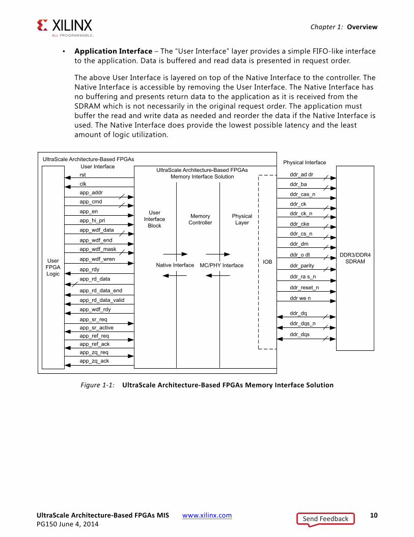
OverviewThe Xilinx® UltraScale™ architecture includes the DDR3/DDR4 SDRAM Memory Interface Solutions (MIS) cores. These MIS cores provide solutions for interfacing with these SDRAM memory types. Both a complete Memory Controller and a physical (PHY) layer only solution are supported. The UltraScale architecture for the DDR3/DDR4 cores are organized in the following high-level blocks.
• Controller – The controller accepts burst transactions from the User Interface and generates transactions to and from the SDRAM. The controller takes care of the SDRAM timing parameters and refresh. It coalesces write and read transactions in order to reduce the dead cycles involved in turning the bus around. The controller also reorders commands to improve the utilization of the data bus to the SDRAM.
• Physical Layer – The physical layer provides a high-speed interface to the SDRAM. This layer includes the hard blocks inside the FPGA and the soft blocks calibration logic necessary to ensure optimal timing of the hard blocks interfacing to the SDRAM.
The new hard blocks in the UltraScale architecture allow interface rates of up to 2,400 Mb/s to be achieved. The application logic is responsible for all SDRAM transactions, timing, and refresh.
° These hard blocks include:
- Data serialization and transmission
- Data capture and deserialization
- High-speed clock generation and synchronization
- Coarse and fine delay elements per pin with voltage and temperature tracking
° The soft blocks include:
- Memory Initialization – The calibration modules provide a JEDEC®-compliant initialization routine for the particular memory type. The delays in the initialization process may be bypassed to speed up simulation time if desired.
- Calibration – The calibration modules provide a complete method to set all delays in the hard blocks and soft IP to work with the memory interface. Each bit is individually trained and then combined in order to ensure optimal interface performance. Results of the calibration process will be available through the Xilinx debug tools. After completion of calibration, the PHY layer presents raw interface to the SDRAM.
Send Feedback
UltraScale Architecture-Based FPGAs MIS www.xilinx.com 10PG150 June 4, 2014
Chapter 1: Overview
• Application Interface – The “User Interface” layer provides a simple FIFO-like interface to the application. Data is buffered and read data is presented in request order.
The above User Interface is layered on top of the Native Interface to the controller. The Native Interface is accessible by removing the User Interface. The Native Interface has no buffering and presents return data to the application as it is received from the SDRAM which is not necessarily in the original request order. The application must buffer the read and write data as needed and reorder the data if the Native Interface is used. The Native Interface does provide the lowest possible latency and the least amount of logic utilization.
X-Ref Target - Figure 1-1
Figure 1-1: UltraScale Architecture-Based FPGAs Memory Interface Solution
Send Feedback
UltraScale Architecture-Based FPGAs MIS www.xilinx.com 11PG150 June 4, 2014
Chapter 1: Overview
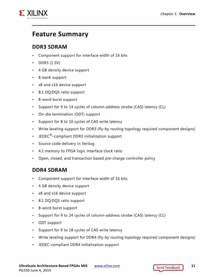
Feature Summary
DDR3 SDRAM• Component support for interface width of 16 bits
• DDR3 (1.5V)
• 4 GB density device support
• 8-bank support
• x8 and x16 device support
• 8:1 DQ:DQS ratio support
• 8-word burst support
• Support for 9 to 14 cycles of column-address strobe (CAS) latency (CL)
• On-die termination (ODT) support
• Support for 8 to 10 cycles of CAS write latency
• Write leveling support for DDR3 (fly-by routing topology required component designs)
• JEDEC®-compliant DDR3 initialization support
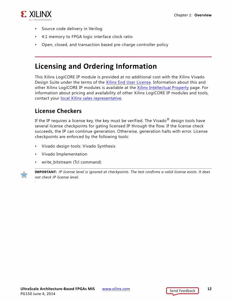
• Source code delivery in Verilog
• 4:1 memory to FPGA logic interface clock ratio
• Open, closed, and transaction based pre-charge controller policy
DDR4 SDRAM• Component support for interface width of 16 bits
• 4 GB density device support
• x8 and x16 device support
• 8:1 DQ:DQS ratio support
• 8-word burst support
• Support for 9 to 24 cycles of column-address strobe (CAS) latency (CL)
• ODT support
• Support for 9 to 18 cycles of CAS write latency
• Write leveling support for DDR4 (fly-by routing topology required component designs)
• JEDEC-compliant DDR4 initialization support
Send Feedback
UltraScale Architecture-Based FPGAs MIS www.xilinx.com 12PG150 June 4, 2014
Chapter 1: Overview
• Source code delivery in Verilog
• 4:1 memory to FPGA logic interface clock ratio
• Open, closed, and transaction based pre-charge controller policy
Licensing and Ordering InformationThis Xilinx LogiCORE IP module is provided at no additional cost with the Xilinx Vivado Design Suite under the terms of the Xilinx End User License. Information about this and other Xilinx LogiCORE IP modules is available at the Xilinx Intellectual Property page. For information about pricing and availability of other Xilinx LogiCORE IP modules and tools, contact your local Xilinx sales representative.
License CheckersIf the IP requires a license key, the key must be verif ied. The Vivado® design tools have several license checkpoints for gating licensed IP through the flow. If the license check succeeds, the IP can continue generation. Otherwise, generation halts with error. License checkpoints are enforced by the following tools:
• Vivado design tools: Vivado Synthesis
• Vivado Implementation
• write_bitstream (Tcl command)
IMPORTANT: IP license level is ignored at checkpoints. The test confirms a valid license exists. It does not check IP license level.
Send Feedback
UltraScale Architecture-Based FPGAs MIS www.xilinx.com 13PG150 June 4, 2014
Chapter 2
Product Specification
StandardsThis core complies to the JESD79-3F, DDR3 SDRAM Standard and JESD79-4, DDR4 SDRAM Standard, JEDEC® Solid State Technology Association [Ref 1].
For more information on UltraScale™ architecture documents, see References, page 155.
Performance
Maximum FrequenciesFor more information on the maximum frequencies, see Kintex UltraScale Architecture Data Sheet, DC and AC Switching Characteristics (DS892) [Ref 2].
Resource Utilization
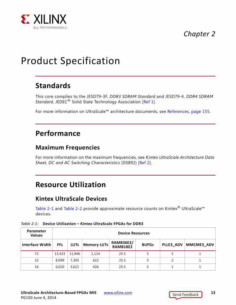
Kintex UltraScale DevicesTable 2-1 and Table 2-2 provide approximate resource counts on Kintex® UltraScale™ devices.
Table 2-1: Device Utilization – Kintex UltraScale FPGAs for DDR3
Parameter Values Device Resources
Interface Width FFs LUTs Memory LUTs RAMB36E2/RAMB18E2 BUFGs PLLE3_ADV MMCME3_ADV
72 13,423 11,940 1,114 25.5 5 3 1
32 8,099 7,305 622 25.5 5 2 1
16 6,020 5,621 426 25.5 5 1 1
Send Feedback
UltraScale Architecture-Based FPGAs MIS www.xilinx.com 14PG150 June 4, 2014
Chapter 2: Product Specification
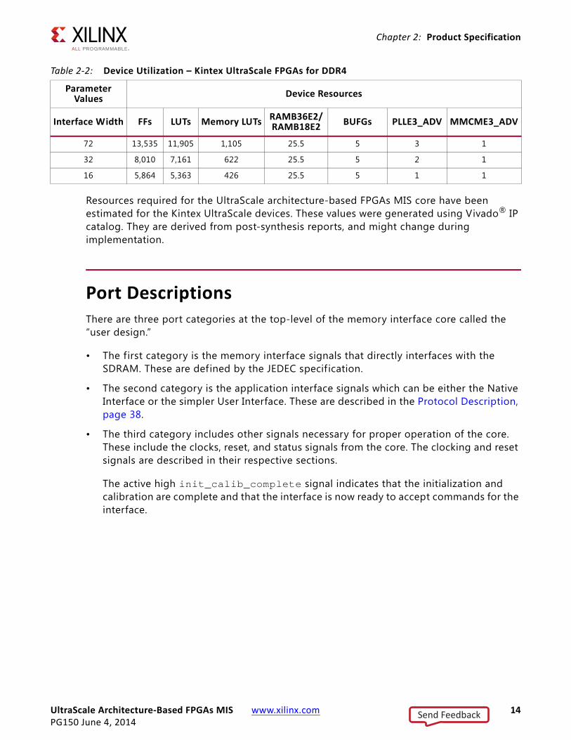
Resources required for the UltraScale architecture-based FPGAs MIS core have been estimated for the Kintex UltraScale devices. These values were generated using Vivado® IP catalog. They are derived from post-synthesis reports, and might change during implementation.
Port DescriptionsThere are three port categories at the top-level of the memory interface core called the “user design.”
• The first category is the memory interface signals that directly interfaces with the SDRAM. These are defined by the JEDEC specif ication.
• The second category is the application interface signals which can be either the Native Interface or the simpler User Interface. These are described in the Protocol Description, page 38.
• The third category includes other signals necessary for proper operation of the core. These include the clocks, reset, and status signals from the core. The clocking and reset signals are described in their respective sections.
The active high init_calib_complete signal indicates that the initialization and calibration are complete and that the interface is now ready to accept commands for the interface.
Table 2-2: Device Utilization – Kintex UltraScale FPGAs for DDR4
Parameter Values Device Resources
Interface Width FFs LUTs Memory LUTs RAMB36E2/RAMB18E2 BUFGs PLLE3_ADV MMCME3_ADV
72 13,535 11,905 1,105 25.5 5 3 1
32 8,010 7,161 622 25.5 5 2 1
16 5,864 5,363 426 25.5 5 1 1
Send Feedback
UltraScale Architecture-Based FPGAs MIS www.xilinx.com 15PG150 June 4, 2014
Chapter 3
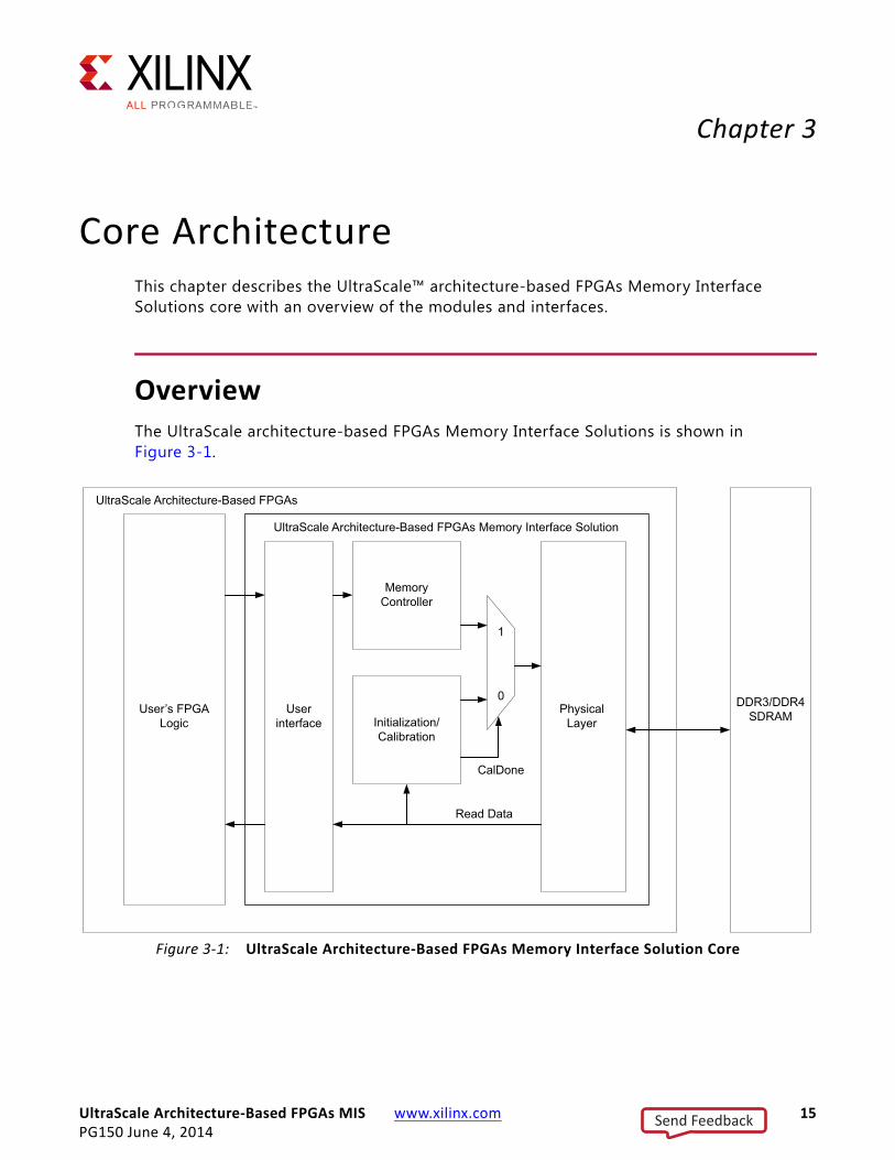
Core ArchitectureThis chapter describes the UltraScale™ architecture-based FPGAs Memory Interface Solutions core with an overview of the modules and interfaces.
OverviewThe UltraScale architecture-based FPGAs Memory Interface Solutions is shown in Figure 3-1.
X-Ref Target - Figure 3-1
Figure 3-1: UltraScale Architecture-Based FPGAs Memory Interface Solution Core
Send Feedback
UltraScale Architecture-Based FPGAs MIS www.xilinx.com 16PG150 June 4, 2014
Chapter 3: Core Architecture
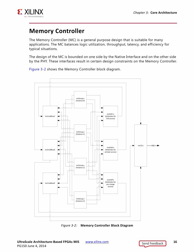
Memory ControllerThe Memory Controller (MC) is a general purpose design that is suitable for many applications. The MC balances logic utilization, throughput, latency, and eff iciency for typical situations.
The design of the MC is bounded on one side by the Native Interface and on the other side by the PHY. These interfaces result in certain design constraints on the Memory Controller.
Figure 3-2 shows the Memory Controller block diagram.
X-Ref Target - Figure 3-2
Figure 3-2: Memory Controller Block Diagram
Send Feedback
UltraScale Architecture-Based FPGAs MIS www.xilinx.com 17PG150 June 4, 2014
Chapter 3: Core Architecture
Native InterfaceThe Native Interface does not offer any opportunity of pipelining data, either read or write. On writes, data is requested one cycle before it is needed by presenting the data buffer address and the data is expected to be supplied on the next cycle. Hence there is no buffering of any kind for data (except due to the barrel shifting to place the data on a particular DDR clock).
On reads, the data is offered by the MC on the cycle it is available. Read data, along with a buffer address is presented on the Native Interface as soon as it is ready. The data has to be accepted by the Native Interface master.
Read and write transactions are mapped to an mcGroup instance based on bank group and bank address bits. Although there are no groups in DDR3, the name group represents either a real group in DDR4 x4 and x8 devices (which serves four banks of that group). For DDR3, each mcGroup module would service two banks. In case of DDR4 x16 interface, the mcGroup represents 1-bit of group (there are only one group bit in x16) and 1-bit of bank, whereby the mcGroup serves two banks.
The total number of outstanding requests depends on the number of mcGroup instances, as well as the round trip delay from the controller to memory and back. When the controller issues an SDRAM CAS command to memory, an mcGroup instance becomes available to take a new request, while the previous CAS commands, read return data, or write data might still be in flight.
Control and Datapaths
Control Path
The control path starts at the mcGroup instances. Each instance can buffer and dispatch one transaction at a time. The mapping of SDRAM group and bank addresses to mcGroup instance ensures that transactions to the same full address map to the same mcGroup instance. Because each mcGroup instance processes the transactions it receives in order, read-after-write and write-after-write address hazards are prevented.
Datapath
The read and write data do not pass through the Memory Controller at all, but are directly connected to the mcCal module. The MC generates the requisite control signals to the mcRead and mcWrite modules telling them the timing of read and write data. The two modules acquire or provide the data as required at the right time.
Send Feedback
UltraScale Architecture-Based FPGAs MIS www.xilinx.com 18PG150 June 4, 2014
Chapter 3: Core Architecture
Read and Write CoalescingThe controller prioritizes reads over writes when reordering is enabled. If both read and write CAS commands are safe to issue on the SDRAM command bus, the controller selects only read CAS commands for arbitration. When a read CAS issues, write CAS commands are blocked for several SDRAM clocks specified by parameter tRTW. The minimum tRTW should be programmed to tCCD + 2tCK + RL – WL. The extra 2tCK allows for turning the data bus around. This extra time required for a write CAS to become safe after issuing a read CAS allows groups of reads to issue on the command bus without being interrupted by pending writes.
ReorderingRequests that map to the same mcGroup are never reordered. Reordering between the mcGroup instances is controlled with the ORDERING parameter. When set to "NORM" reordering is enabled and the arbiter implements a round-robin priority plan, selecting in priority order among the mcGroups with a command that is safe to issue to the SDRAM. The timing of when it is safe to issue a command to the SDRAM can vary on the target bank or bank group and its page status. This often contributes to reordering.
When the ORDERING parameter is set to "STRICT," all requests have their CAS commands issued in the order in which the requests were accepted at the Native Interface. STRICT ordering overrides all other controller mechanisms, such as the tendency to coalesce read requests, and can therefore degrade data bandwidth utilization in some workloads.
Group MachinesIn the Memory Controller, there are four group state machines. These state machines are allocated depending on technology (DDR3 or DDR4) and width (x4, x8, and x16). The following summarizes the allocation to each group machine. In this description, GM refers to the Group Machine (0 to 3), BG refers to group address, and BA refers to bank address. Note that group in the context of a group state machine denotes a notional group and does not necessarily refer to a real group (except in case of DDR4, part x4 and x8).
Send Feedback
UltraScale Architecture-Based FPGAs MIS www.xilinx.com 19PG150 June 4, 2014
Chapter 3: Core Architecture
• DDR3, any part – Total of eight banks
° GM 0: BA[2:1] == 2'b00; services banks 0 and 1
° GM 1: BA[2:1] == 2'b01; services banks 2 and 3
° GM 2: BA[2:1] == 2'b10; services banks 4 and 5
° GM 3: BA[2:1] == 2'b11; services banks 6 and 7
• DDR4, x4 and x8 parts – Total of 16 banks
° GM 0: services BG 0; four banks per group
° GM 1: services BG 1; four banks per group
° GM 2: services BG 2; four banks per group
° GM 3: services BG 3; four banks per group
• DDR4, x16 parts – Total of eight banks
° GM 0: services BG 0, BA[0] == 0; 2 banks per group
° GM 1: services BG 0, BA[0] == 1; 2 banks per group
° GM 2: services BG 1, BA[0] == 0; 2 banks per group
° GM 3: services BG 1, BA[0] == 1; 2 banks per group
PHYPHY is considered the low-level physical interface to an external DDR3 or DDR4 SDRAM device as well as all calibration logic for ensuring reliable operation of the physical interface itself. PHY generates the signal timing and sequencing required to interface to the memory device.
PHY contains the following features:
• Clock/address/control-generation logics
• Write and read datapaths
• Logic for initializing the SDRAM after power-up
In addition, PHY contains calibration logic to perform timing training of the read and write datapaths to account for system static and dynamic delays.
Send Feedback
UltraScale Architecture-Based FPGAs MIS www.xilinx.com 20PG150 June 4, 2014
Chapter 3: Core Architecture
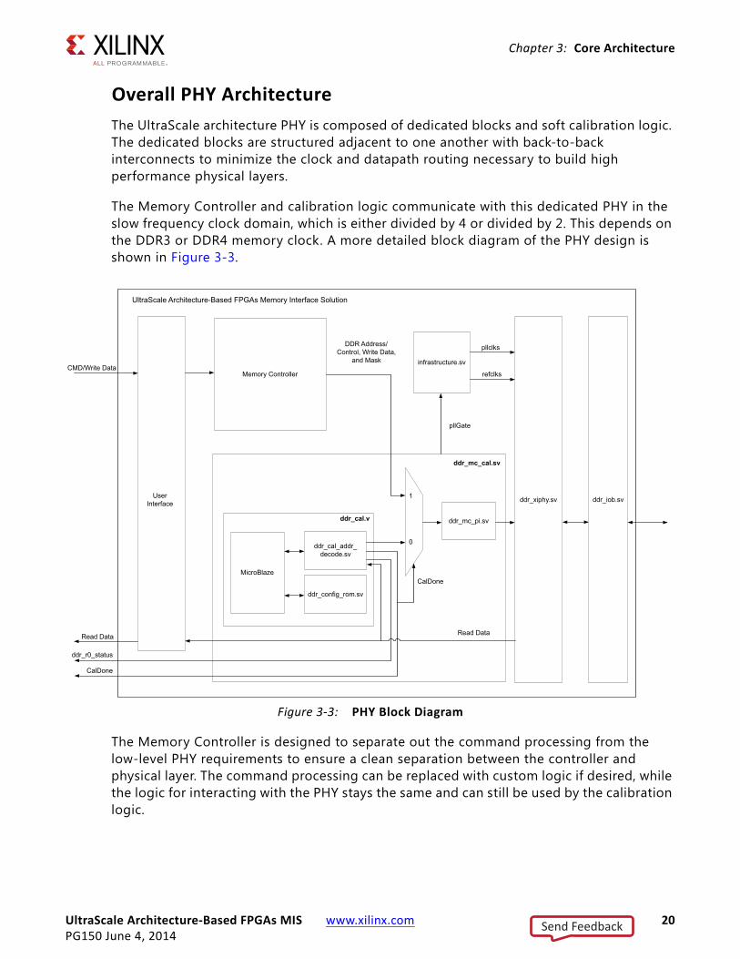
Overall PHY ArchitectureThe UltraScale architecture PHY is composed of dedicated blocks and soft calibration logic. The dedicated blocks are structured adjacent to one another with back-to-back interconnects to minimize the clock and datapath routing necessary to build high performance physical layers.
The Memory Controller and calibration logic communicate with this dedicated PHY in the slow frequency clock domain, which is either divided by 4 or divided by 2. This depends on the DDR3 or DDR4 memory clock. A more detailed block diagram of the PHY design is shown in Figure 3-3.
The Memory Controller is designed to separate out the command processing from the low-level PHY requirements to ensure a clean separation between the controller and physical layer. The command processing can be replaced with custom logic if desired, while the logic for interacting with the PHY stays the same and can still be used by the calibration logic.
X-Ref Target - Figure 3-3
Figure 3-3: PHY Block Diagram
Send Feedback
UltraScale Architecture-Based FPGAs MIS www.xilinx.com 21PG150 June 4, 2014
Chapter 3: Core Architecture
The PHY architecture encompasses all of the logic contained in ddr_phy.sv. The PHY contains wrappers around dedicated hard blocks to build up the memory interface from smaller components. A byte lane contains all of the clocks, resets, and datapaths for a given subset of I/O. Multiple byte lanes are grouped together, along with dedicated clocking resources, to make up a single bank memory interface. For more information on the hard silicon physical layer architecture, see the UltraScale™ Architecture-Based FPGAs SelectIO™ Resources User Guide (UG571) [Ref 3].
The memory initialization is executed in Verilog RTL. The calibration and training are implemented by an embedded MicroBlaze™ processor. The MicroBlaze Controller System (MCS) is configured with an I/O Module and a block RAM. The ddr_cal_addr_decode.sv module provides the interface for the processor to the rest of the system and implements helper logic. The ddr_config_rom.sv module stores settings that control the operation of initialization and calibration, providing run time options that can be adjusted without having to recompile the source code.
The address unit connects the MCS to the local register set and the PHY by performing address decode and control translation on the I/O module bus from spaces in the memory map and MUXing return data (ddr_cal_addr_decode.sv). In addition, it provides address translation (also known as “mapping”) from a logical conceptualization of the DRAM interface to the appropriate pinout-dependent location of the delay control in the PHY address space.
Table 3-1: PHY Modules
Module Name Description
ddr_mc_cal.sv Contains ddr_cal.sv, ddr_mc_pi.sv, and MUXes between the calibration and the Memory Controller.
ddr_cal.sv Contains the MicroBlaze processing system and associated logic.
ddr_mc_pi.sv Adjusts signal timing for the PHY for reads and writes.
ddr_cal_addr_decode.sv FPGA logic interface for the MicroBlaze processor.
ddr_config_rom.sv Configuration storage for calibration options.
microblaze MicroBlaze processor
ddr_iob.sv Instantiates all byte IOB modules
ddr_iob_byte.sv Generates the I/O buffers for all the signals in a given byte lane.
ddr_debug_microblaze.sv Simulation-only f ile to parse debug statements from software running in MicroBlaze to indicate status and calibration results to the log.
ddr_cal_cplx.sv RTL state machine for complex pattern calibration.
ddr_cal_cplx_data.sv Data patterns used for complex pattern calibration.
ddr_xiphy.sv Top-level XIPHY module
ddr_phy.sv Top-level of the PHY, contains ddr_mc_cal.sv and ddr_xiphy.sv modules.
Send Feedback
UltraScale Architecture-Based FPGAs MIS www.xilinx.com 22PG150 June 4, 2014
Chapter 3: Core Architecture
Although the calibration architecture presents a simple and organized address map for manipulating the delay elements for individual data, control and command bits, there is flexibility in how those I/O pins are placed. For a given I/O placement, the path to the FPGA logic is locked to a given pin. To enable a single binary software f ile to work with any memory interface pinout, a translation block converts the simplif ied RIU addressing into the pinout-specific RIU address for the target design. The specif ic address translation is written by MIG after a pinout is selected and cannot be modif ied. The code shows an example of the RTL structure that supports this.
Casez(io_address)// MicroBlaze I/O module address // … static address decoding skipped //========================================// //===========DQ ODELAYS===================// //========================================// //Byte0 28’h0004100: begin //dq2 riu_addr_cal = /* MIG Generated */ 6’hd; riu_nibble = /* MIG Generated */ ‘h0; end // … additional dynamic addressing follows
In this example, DQ0 is pinned out on Bit[0] of nibble 0 (nibble 0 according to instantiation order). The RIU address for the ODELAY for Bit[0] is 0x0D (for more details on the RIU address map, see the RIU specification). When DQ0 is addressed — indicated by address 0x000_4100), this snippet of code is active. It enables nibble 0 (decoded to one-hot downstream) and forwards the address 0x0D to the RIU address bus.
The MicroBlaze I/O module interface updates at a maximum rate of once every three clock cycles, which is not always fast enough for implementing all of the functions required in calibration. A helper circuit implemented in ddr_cal_addr_decode.sv is required to obtain commands from the registers and translate at least a portion into single-cycle accuracy for submission to the PHY. In addition, it supports command repetition to enable back-to-back read transactions and read data comparison.
Send Feedback
UltraScale Architecture-Based FPGAs MIS www.xilinx.com 23PG150 June 4, 2014
Chapter 3: Core Architecture
Memory Initialization and Calibration SequenceAfter deassertion of the system reset, PHY performs some required internal calibration steps first.
1. Start an I/O offset calibration. This performs an internal adjustment of each single-ended pin to cancel any inherent offsets between single-ended and differential buffers.
2. After I/O offset calibration is completed, the built-in self-check of the PHY (BISC) is run.
3. BISC is used in the PHY to compute internal skews for use in voltage and temperature tracking after calibration is completed.
4. After BISC is completed, calibration logic performs the required power-on initialization sequence for the memory. This is followed by several stages of timing calibration for the write and read datapaths.
5. After calibration is completed, PHY calculates internal offsets to be used in voltage and temperature tracking.
6. PHY indicates calibration is f inished and the controller begins issuing commands to the memory.
Send Feedback
UltraScale Architecture-Based FPGAs MIS www.xilinx.com 24PG150 June 4, 2014
Chapter 3: Core Architecture
Figure 3-4 shows the overall flow of memory initialization and the different stages of calibration.
X-Ref Target - Figure 3-4
Figure 3-4: PHY Overall Initialization and Calibration Sequence
Send Feedback
UltraScale Architecture-Based FPGAs MIS www.xilinx.com 25PG150 June 4, 2014
Chapter 3: Core Architecture
When simulating a design out of MIG, the calibration it set to be bypassed to enable you to generate traff ic to and from the DRAM as quickly as possible. When running in hardware or simulating with calibration, enabled signals are provided to indicate what step of calibration is running or, if an error occurs, where an error occurred.
The first step in determining calibration status is to check the CalDone port. After the CalDone port is checked, the status bits should be checked to indicate the steps that were ran and completed. Calibration halts on the very f irst error encountered, so the status bits indicate which step of calibration was last run. The status and error signals can be checked through either connecting the Vivado analyzer signals to these ports or through the XSDB tool (also through Vivado).
Send Feedback

UltraScale Architecture-Based FPGAs MIS www.xilinx.com 26PG150 June 4, 2014
Chapter 4
Designing with the CoreThis chapter includes guidelines and additional information to facilitate designing with the core.
ClockingThe memory interface requires one MMCM, one TXPLL per I/O bank used by the memory interface, two BUFGs, and one BUFGCE_DIV. These clocking components are used to create the proper clock frequencies and phase shifts necessary for the proper operation of the memory interface.
There are two TXPLLs per bank. If a bank is shared by two memory interfaces, both TXPLLs in that bank are used.
Note: MIG generates the appropriate clocking structure and no modifications to the RTL are supported.
The MIG tool generates the appropriate clocking structure for the desired interface. This structure must not be modif ied. The allowed clock configuration is as follows:
• Differential reference clock source connected to GCIO
• GCIO to MMCM (located in same bank as GCIO)
• MMCM to BUFG (located in same bank as MMCM)
• BUFG (at MMCM) to BUFG (located at center bank of memory interface) driving FPGA logic and all TXPLLs
• BUFG (at MMCM) to BUFGCE_DIV (located at center bank of memory interface) divide by two mode driving 1/2 rate FPGA logic
• Clocking pair of the interface must be in the same SLR of memory interface for the SSI technology devices
Send Feedback

UltraScale Architecture-Based FPGAs MIS www.xilinx.com 27PG150 June 4, 2014
Chapter 4: Designing with the Core
Requirements
GCIO
• Must use a differential I/O standard
• Must be in the same I/O column as the memory interface
MMCM
• MMCM is used to generate the FPGA logic system clock (1/4 of the memory clock)
• Must be located in the same bank as the GCIO
• Must use internal feedback
• Input clock frequency divided by input divider must be ≥ 70 MHz (CLKINx / D ≥ 70 MHz)
• Must use integer multiply and output divide values
BUFG and Clock Root at MMCM
• Must be placed in the same bank as the MMCM
BUFG/BUFGCE_DIV and Clock Roots
• BUFGCE_DIV is used to divide the system clock by two.
• BUFGCE_DIV and BUFG and clock roots must be located in center most bank of the memory interface.
° For two bank systems, either bank can be used. MIG is always referred to the top-most selected bank in the GUI as the center bank.
° For four bank systems, either of the center banks can be chosen. MIG refers to the second bank from the top-most selected bank as the center bank.
° BUFG and BUFGCE_DIV must be in the same bank.
TXPLL
• CLKOUTPHY from TXPLL drives XiPhy within its bank
• TXPLL must be set to use a CLKFBOUT phase shift of 90°
• TXPLL must be held in reset until the MMCM lock output goes High
• Must use internal feedback
Send Feedback

UltraScale Architecture-Based FPGAs MIS www.xilinx.com 28PG150 June 4, 2014
Chapter 4: Designing with the Core
Figure 4-1 shows an example of the clocking structure for a three bank memory interface. The GCIO drives the MMCM in the fourth bank which in turn drives a clock through a BUFG to bank 2 in the center of the memory interface. This clock drives both a BUFG and BUFGCE_DIV located in this bank. The BUFG output drives the TXPLLs used in each bank of the interface.
ResetsAn asynchronous reset input is provided. This active-High reset must assert for a minimum of 20 cycles of the controller clock.
X-Ref Target - Figure 4-1
Figure 4-1: Clocking Structure for Three Bank Memory Interface
Send Feedback
UltraScale Architecture-Based FPGAs MIS www.xilinx.com 29PG150 June 4, 2014
Chapter 4: Designing with the Core
PCB Guidelines for DDR3Strict adherence to all documented DDR3 PCB guidelines is required for successful operation. For more information on PCB guidelines, see the UltraScale Architecture PCB Design and Pin Planning User Guide (UG583) [Ref 4].
PCB Guidelines for DDR4Strict adherence to all documented DDR4 PCB guidelines is required for successful operation. For more information on PCB guidelines, see the UltraScale Architecture PCB Design and Pin Planning User Guide (UG583) [Ref 4].
Pin and Bank Rules
DDR3 Pin RulesThe rules are for single rank memory interfaces. For multi-rank information, contact Xilinx®.
• Address/control means cs_n, ras_n, cas_n, we_n, ba, ck , cke, a, and odt.
• Pins in a byte lane are numbered N0 to N12.
• Byte lanes in a bank are designed by T0, T1, T2, or T3. Nibbles within a byte lane are distinguished by a “U” or “L” designator added to the byte lane designator (T0, T1, T2, or T3). Thus they are T0L, T0U, T1L, T1U, T2L, T2U, T3L, and T3U.
Note: There are two PLLs per bank and a controller uses one PLL in every bank that is being used by the interface.
1. dqs, dq, and dm location.
a. Designs using x8 or x16 components – dqs must be located on a dedicated byte clock pair in the upper nibble designated with “U.” dq associated with a dqs must be in same byte lane on any of the other pins except pins 1 and 12.
b. Designs using x4 components – dqs must be located on a dedicated byte clock pair in the nibble. dq associated with a dqs must be in same nibble on any of the other pins except pins N1 (lower nibble) and pin N12 (upper nibble).
c. dm (if used) must be located on pin N0 in the byte lane with the corresponding dqs.
2. Byte lanes are configured as either data or address/control.
a. Pins N1 and N12 can be used for address/control in a data byte lane.
Send Feedback
UltraScale Architecture-Based FPGAs MIS www.xilinx.com 30PG150 June 4, 2014
Chapter 4: Designing with the Core
b. No data signals (dqs, dq, dm) can be placed in an address/control byte lane.
3. Address/control can be on any of the 13 pins in the address/control byte lanes. Address/control must be contained within the same bank.
4. There is one vr pin per bank and DCI is required. DCI cascade is not permitted. All rules for the DCI in the UltraScale™ Architecture-Based FPGAs SelectIO™ Resources User Guide (UG571) [Ref 3] must be followed.
5. ck must be on the PN pair in the Address/Control byte lane.
6. reset_n can only be allocated within the memory interface banks.
7. Banks can be shared between two controllers.
a. Each byte lane is dedicated to a specific controller (except for reset_n).
b. Byte lanes from one controller cannot be placed inside the other. For example, with controllers A and B, “AABB” is allowed, while “ABAB” is not.
8. All I/O banks used by the memory interface must be in the same column.
9. All I/O banks used by the memory interface must be in the same SLR of the column for the SSI technology devices.
10. Maximum height of interface is f ive contiguous banks for 144-bit wide interface.
11. Bank skipping is not allowed.
12. The input clock for the master PLL in the interface must come from the a clock capable pair in the I/O column used for the memory interface.
13. There are dedicated VREF pins (not included in the rules above). Either internal or external VREF is permitted. If an external VREF is not used, the VREF pins should be pulled to ground by a 500Ω resistor. For more information, see the UltraScale™ Architecture-Based FPGAs SelectIO™ Resources User Guide (UG571) [Ref 3]. These pins must be connected appropriately for the standard in use.
14. The interface must be contained within the same I/O bank type (High Range or High Performance). Mixing bank types is not permitted with the exceptions of the reset_n in step 6 above and the input clock mentioned in step 11 above.
DDR3 Pinout Examples
IMPORTANT: Due to the calibration stage, there is no need for set_input_delay/set_output_delay on the MIG. You need to ignore the unconstrained inputs and outputs for MIG and the signals which are calibrated.
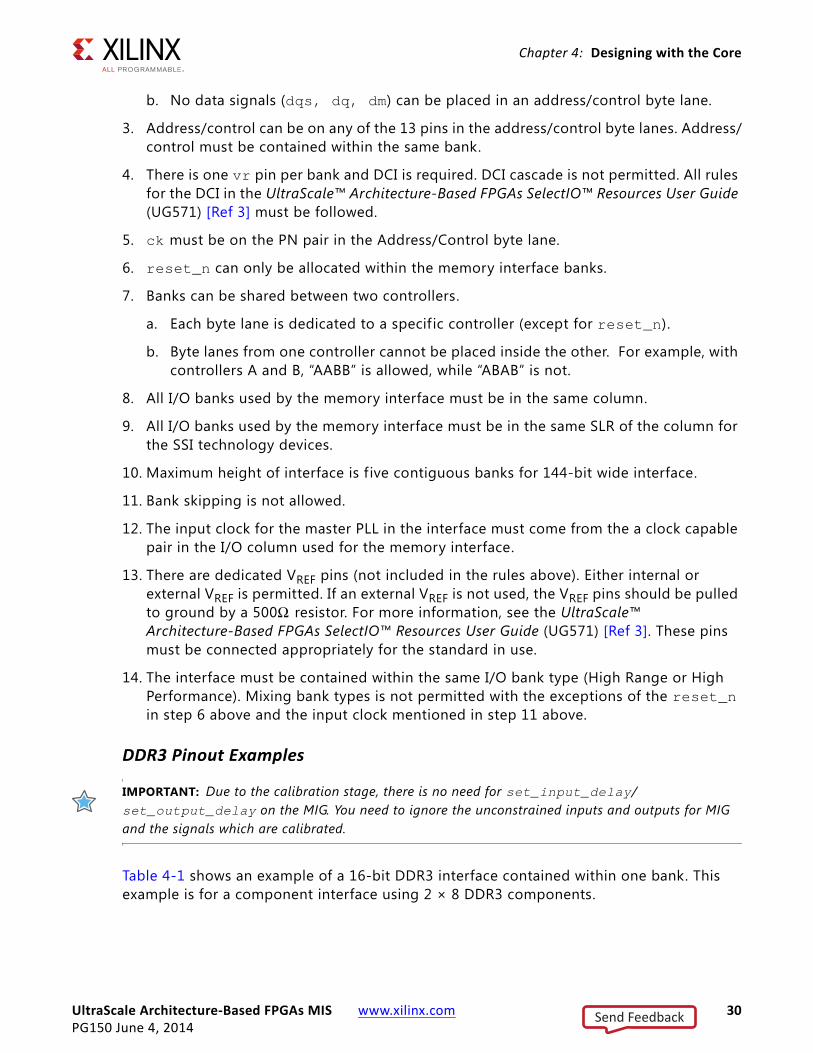
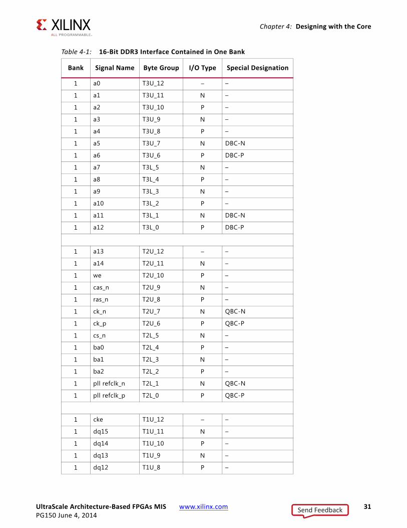
Table 4-1 shows an example of a 16-bit DDR3 interface contained within one bank. This example is for a component interface using 2 × 8 DDR3 components.
Send Feedback
UltraScale Architecture-Based FPGAs MIS www.xilinx.com 31PG150 June 4, 2014
Chapter 4: Designing with the Core
Table 4-1: 16-Bit DDR3 Interface Contained in One Bank
Bank Signal Name Byte Group I/O Type Special Designation
1 a0 T3U_12 – –
1 a1 T3U_11 N –
1 a2 T3U_10 P –
1 a3 T3U_9 N –
1 a4 T3U_8 P –
1 a5 T3U_7 N DBC-N
1 a6 T3U_6 P DBC-P
1 a7 T3L_5 N –
1 a8 T3L_4 P –
1 a9 T3L_3 N –
1 a10 T3L_2 P –
1 a11 T3L_1 N DBC-N
1 a12 T3L_0 P DBC-P
1 a13 T2U_12 – –
1 a14 T2U_11 N –
1 we T2U_10 P –
1 cas_n T2U_9 N –
1 ras_n T2U_8 P –
1 ck_n T2U_7 N QBC-N
1 ck_p T2U_6 P QBC-P
1 cs_n T2L_5 N –
1 ba0 T2L_4 P –
1 ba1 T2L_3 N –
1 ba2 T2L_2 P –
1 pll refclk_n T2L_1 N QBC-N
1 pll refclk_p T2L_0 P QBC-P
1 cke T1U_12 – –
1 dq15 T1U_11 N –
1 dq14 T1U_10 P –
1 dq13 T1U_9 N –
1 dq12 T1U_8 P –
Send Feedback
UltraScale Architecture-Based FPGAs MIS www.xilinx.com 32PG150 June 4, 2014
Chapter 4: Designing with the Core
DDR4 Pin RulesThe rules are for single rank memory interfaces. For multi-rank information, contact Xilinx.
• Address/control means cs_n, ras_n, cas_n, we_n, ba, bg, ck , cke, a, odt, act_n, and par.
• Pins in a byte lane are numbered N0 to N12.
• Byte lanes in a bank are designed by T0, T1, T2, or T3. Nibbles within a byte lane are distinguished by a “U” or “L” designator added to the byte lane designator (T0, T1, T2, or T3). Thus they are T0L, T0U, T1L, T1U, T2L, T2U, T3L, and T3U.
Note: There are two PLLs per bank and a controller uses one PLL in every bank that is being used by the interface.
1 dqs1_n T1U_7 N QBC-N
1 dqs1_p T1U_6 P QBC-P
1 dq11 T1L_5 N –
1 dq10 T1L_4 P –
1 dq9 T1L_3 N –
1 dq8 T1L_2 P –
1 odt T1L_1 N QBC-N
1 dm1 T1L_0 P QBC-P
1 vr T0U_12 – –
1 dq7 T0U_11 N –
1 dq6 T0U_10 P –
1 dq5 T0U_9 N –
1 dq4 T0U_8 P –
1 dqs0_n T0U_7 N DBC-N
1 dqs0_p T0U_6 P DBC-P
1 dq3 T0L_5 N –
1 dq2 T0L_4 P –
1 dq1 T0L_3 N –
1 dq0 T0L_2 P –
1 reset_n T0L_1 N DBC-N
1 dm0 T0L_0 P DBC-P
Table 4-1: 16-Bit DDR3 Interface Contained in One Bank (Cont’d)
Bank Signal Name Byte Group I/O Type Special Designation
Send Feedback
UltraScale Architecture-Based FPGAs MIS www.xilinx.com 33PG150 June 4, 2014
Chapter 4: Designing with the Core
1. dqs, dq, and dm/dbi location.
a. Designs using x8 or x16 components – dqs must be located on a dedicated byte clock pair in the upper nibble designated with “U.” dq associated with a dqs must be in same byte lane on any of the other pins except pins N1 and N12.
b. Designs using x4 components – dqs must be located on a dedicated byte clock pair in the nibble. dq associated with a dqs must be in same nibble on any of the other pins except pins N1 (lower nibble) and pin N12 (upper nibble).
c. dm/dbi must be on pin N0 in the byte lane with the associated dqs.
2. Byte lanes are configured as either data or address/control.
a. Pins N1 and N12 can be used for address/control in a data byte lane.
b. No data signals (dqs, dq, dm/dbi) can be placed in an address/control byte lane.
3. Address/control can be on any of the 13 pins in the address/control byte lanes. Address/control must be contained within the same bank.
4. There is one vr pin per bank and DCI is required. DCI Cascade is not permitted. All rules for the DCI in the UltraScale™ Architecture-Based FPGAs SelectIO™ Resources User Guide (UG571) [Ref 3] must be followed.
5. ck must be on the PN pair in the Address/Control byte lane.
6. reset_n can only be allocated within the memory interface banks.
7. Banks can be shared between two controllers.
a. Each byte lane is dedicated to a specific controller (except for reset_n).
b. Byte lanes from one controller cannot be placed inside the other. For example, with controllers A and B, “AABB” is allowed, while “ABAB” is not.
8. All I/O banks used by the memory interface must be in the same column.
9. All I/O banks used by the memory interface must be in the same SLR of the column for the SSI technology devices.
10. Maximum height of interface is f ive contiguous banks for 144-bit wide interface.
11. Bank skipping is not allowed.
12. The input clock for the master PLL in the interface must come from the a clock capable pair in the I/O column used for the memory interface.
13. The dedicated VREF pins in the banks used for DDR4 must be tied to ground with a 500Ω resistor. Internal VREF is required for DDR4. For more information, see the UltraScale™ Architecture-Based FPGAs SelectIO™ Resources User Guide (UG571) [Ref 3].
14. The interface must be contained within the same I/O bank type (High Range or High Performance). Mixing bank types is not permitted with the exceptions of the reset_n in step 6 above and the input clock mentioned in step 11 above.
Send Feedback
UltraScale Architecture-Based FPGAs MIS www.xilinx.com 34PG150 June 4, 2014
Chapter 4: Designing with the Core
15. The par input for command and address parity and the alert_n input/output are not supported by this interface. Consult the memory vendor for information on the proper connection for these pins when not used.
IMPORTANT: Component interfaces should be created with the same component for all components in the interface. x16 components have a different number of bank groups than the x8 components. For example, a 72-bit wide component interface should be created by using nine x8 components or five x16 components where half of one component is not used. Four x16 components and one x8 component is not permissible.
DDR4 Pinout Examples
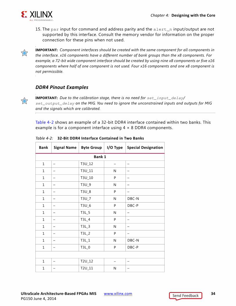
IMPORTANT: Due to the calibration stage, there is no need for set_input_delay/set_output_delay on the MIG. You need to ignore the unconstrained inputs and outputs for MIG and the signals which are calibrated.
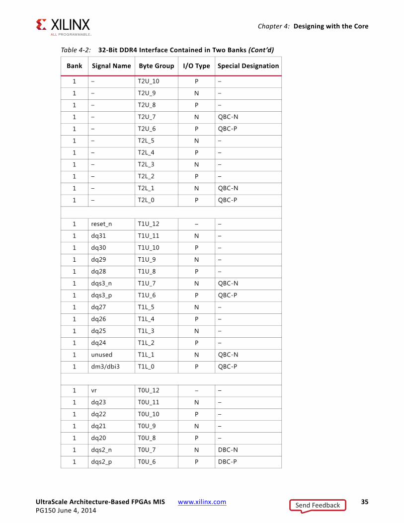
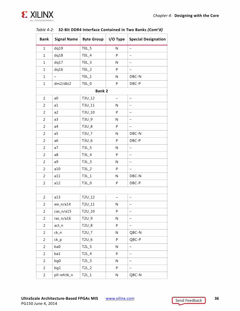
Table 4-2 shows an example of a 32-bit DDR4 interface contained within two banks. This example is for a component interface using 4 × 8 DDR4 components.
Table 4-2: 32-Bit DDR4 Interface Contained in Two Banks
Bank Signal Name Byte Group I/O Type Special Designation
Bank 1
1 – T3U_12 – –
1 – T3U_11 N –
1 – T3U_10 P –
1 – T3U_9 N –
1 – T3U_8 P –
1 – T3U_7 N DBC-N
1 – T3U_6 P DBC-P
1 – T3L_5 N –
1 – T3L_4 P –
1 – T3L_3 N –
1 – T3L_2 P –
1 – T3L_1 N DBC-N
1 – T3L_0 P DBC-P
1 – T2U_12 – –
1 – T2U_11 N –
Send Feedback
UltraScale Architecture-Based FPGAs MIS www.xilinx.com 35PG150 June 4, 2014
Chapter 4: Designing with the Core
1 – T2U_10 P –
1 – T2U_9 N –
1 – T2U_8 P –
1 – T2U_7 N QBC-N
1 – T2U_6 P QBC-P
1 – T2L_5 N –
1 – T2L_4 P –
1 – T2L_3 N –
1 – T2L_2 P –
1 – T2L_1 N QBC-N
1 – T2L_0 P QBC-P
1 reset_n T1U_12 – –
1 dq31 T1U_11 N –
1 dq30 T1U_10 P –
1 dq29 T1U_9 N –
1 dq28 T1U_8 P –
1 dqs3_n T1U_7 N QBC-N
1 dqs3_p T1U_6 P QBC-P
1 dq27 T1L_5 N –
1 dq26 T1L_4 P –
1 dq25 T1L_3 N –
1 dq24 T1L_2 P –
1 unused T1L_1 N QBC-N
1 dm3/dbi3 T1L_0 P QBC-P
1 vr T0U_12 – –
1 dq23 T0U_11 N –
1 dq22 T0U_10 P –
1 dq21 T0U_9 N –
1 dq20 T0U_8 P –
1 dqs2_n T0U_7 N DBC-N
1 dqs2_p T0U_6 P DBC-P
Table 4-2: 32-Bit DDR4 Interface Contained in Two Banks (Cont’d)
Bank Signal Name Byte Group I/O Type Special Designation
Send Feedback
UltraScale Architecture-Based FPGAs MIS www.xilinx.com 36PG150 June 4, 2014
Chapter 4: Designing with the Core
1 dq19 T0L_5 N –
1 dq18 T0L_4 P –
1 dq17 T0L_3 N –
1 dq16 T0L_2 P –
1 – T0L_1 N DBC-N
1 dm2/dbi2 T0L_0 P DBC-P
Bank 2
2 a0 T3U_12 – –
2 a1 T3U_11 N –
2 a2 T3U_10 P –
2 a3 T3U_9 N –
2 a4 T3U_8 P –
2 a5 T3U_7 N DBC-N
2 a6 T3U_6 P DBC-P
2 a7 T3L_5 N –
2 a8 T3L_4 P –
2 a9 T3L_3 N –
2 a10 T3L_2 P –
2 a11 T3L_1 N DBC-N
2 a12 T3L_0 P DBC-P
2 a13 T2U_12 – –
2 we_n/a14 T2U_11 N –
2 cas_n/a15 T2U_10 P –
2 ras_n/a16 T2U_9 N –
2 act_n T2U_8 P –
2 ck_n T2U_7 N QBC-N
2 ck_p T2U_6 P QBC-P
2 ba0 T2L_5 N –
2 ba1 T2L_4 P –
2 bg0 T2L_3 N –
2 bg1 T2L_2 P –
2 pll refclk_n T2L_1 N QBC-N
Table 4-2: 32-Bit DDR4 Interface Contained in Two Banks (Cont’d)
Bank Signal Name Byte Group I/O Type Special Designation
Send Feedback

UltraScale Architecture-Based FPGAs MIS www.xilinx.com 37PG150 June 4, 2014
Chapter 4: Designing with the Core
2 pll refclk T2L_0 P QBC-P
2 cs_n T1U_12 – –
2 dq15 T1U_11 N –
2 dq14 T1U_10 P –
2 dq13 T1U_9 N –
2 dq12 T1U_8 P –
2 dqs1_n T1U_7 N QBC-N
2 dqs1_p T1U_6 P QBC-P
2 dq11 T1L_5 N –
2 dq10 T1L_4 P –
2 dq9 T1L_3 N –
2 dq8 T1L_2 P –
2 odt T1L_1 N QBC-N
2 dm1/dbi1 T1L_0 P QBC-P
2 vr T0U_12 – –
2 dq7 T0U_11 N –
2 dq6 T0U_10 P –
2 dq5 T0U_9 N –
2 dq4 T0U_8 P –
2 dqs0_n T0U_7 N DBC-N
2 dqs0_p T0U_6 P DBC-P
2 dq3 T0L_5 N –
2 dq2 T0L_4 P –
2 dq1 T0L_3 N –
2 dq0 T0L_2 P –
2 cke T0L_1 N DBC-N
2 dm0/dbi0 T0L_0 P DBC-P
Table 4-2: 32-Bit DDR4 Interface Contained in Two Banks (Cont’d)
Bank Signal Name Byte Group I/O Type Special Designation
Send Feedback
UltraScale Architecture-Based FPGAs MIS www.xilinx.com 38PG150 June 4, 2014
Chapter 4: Designing with the Core
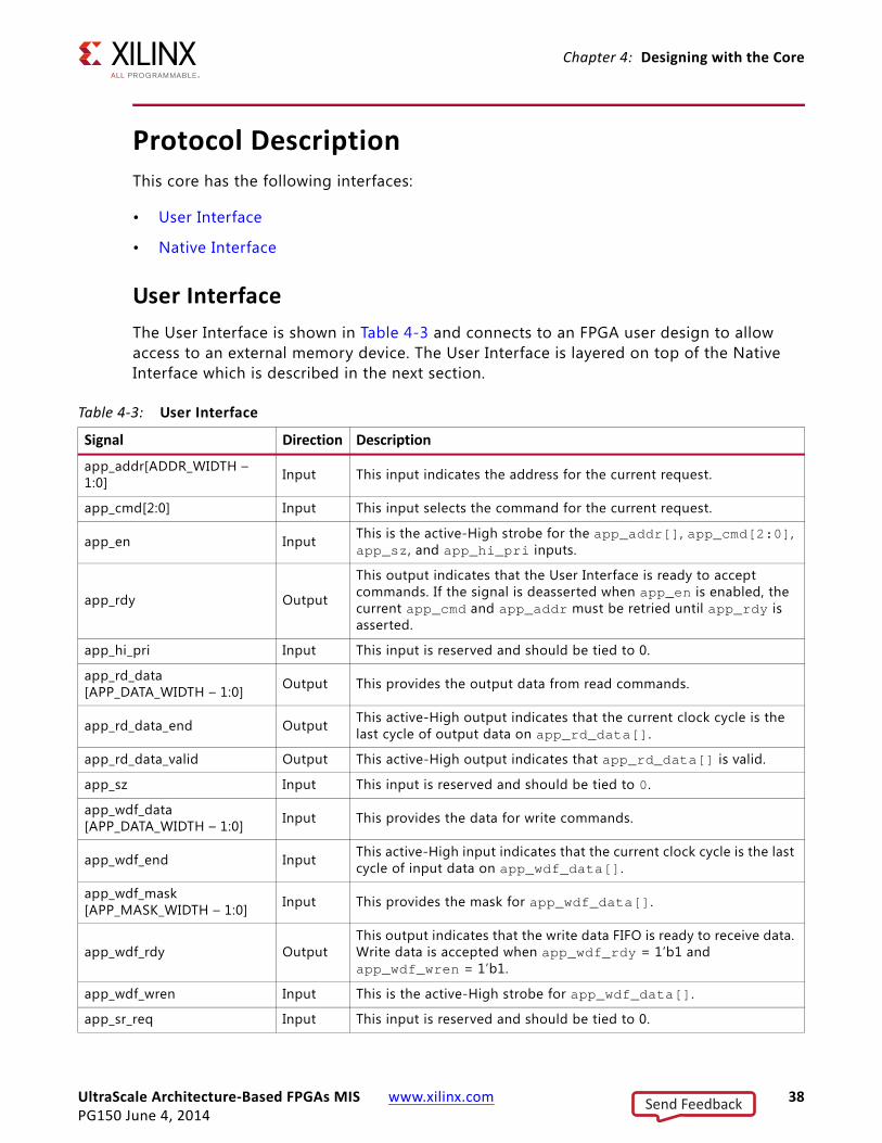
Protocol DescriptionThis core has the following interfaces:
• User Interface
• Native Interface
User InterfaceThe User Interface is shown in Table 4-3 and connects to an FPGA user design to allow access to an external memory device. The User Interface is layered on top of the Native Interface which is described in the next section.
Table 4-3: User Interface
Signal Direction Description
app_addr[ADDR_WIDTH – 1:0] Input This input indicates the address for the current request.
app_cmd[2:0] Input This input selects the command for the current request.
app_en Input This is the active-High strobe for the app_addr[], app_cmd[2:0], app_sz, and app_hi_pri inputs.
app_rdy Output
This output indicates that the User Interface is ready to accept commands. If the signal is deasserted when app_en is enabled, the current app_cmd and app_addr must be retried until app_rdy is asserted.
app_hi_pri Input This input is reserved and should be tied to 0.
app_rd_data[APP_DATA_WIDTH – 1:0] Output This provides the output data from read commands.
app_rd_data_end Output This active-High output indicates that the current clock cycle is the last cycle of output data on app_rd_data[].
app_rd_data_valid Output This active-High output indicates that app_rd_data[] is valid.
app_sz Input This input is reserved and should be tied to 0.
app_wdf_data[APP_DATA_WIDTH – 1:0] Input This provides the data for write commands.
app_wdf_end Input This active-High input indicates that the current clock cycle is the last cycle of input data on app_wdf_data[].
app_wdf_mask[APP_MASK_WIDTH – 1:0] Input This provides the mask for app_wdf_data[].
app_wdf_rdy OutputThis output indicates that the write data FIFO is ready to receive data. Write data is accepted when app_wdf_rdy = 1’b1 and app_wdf_wren = 1’b1.
app_wdf_wren Input This is the active-High strobe for app_wdf_data[].
app_sr_req Input This input is reserved and should be tied to 0.
Send Feedback
UltraScale Architecture-Based FPGAs MIS www.xilinx.com 39PG150 June 4, 2014
Chapter 4: Designing with the Core
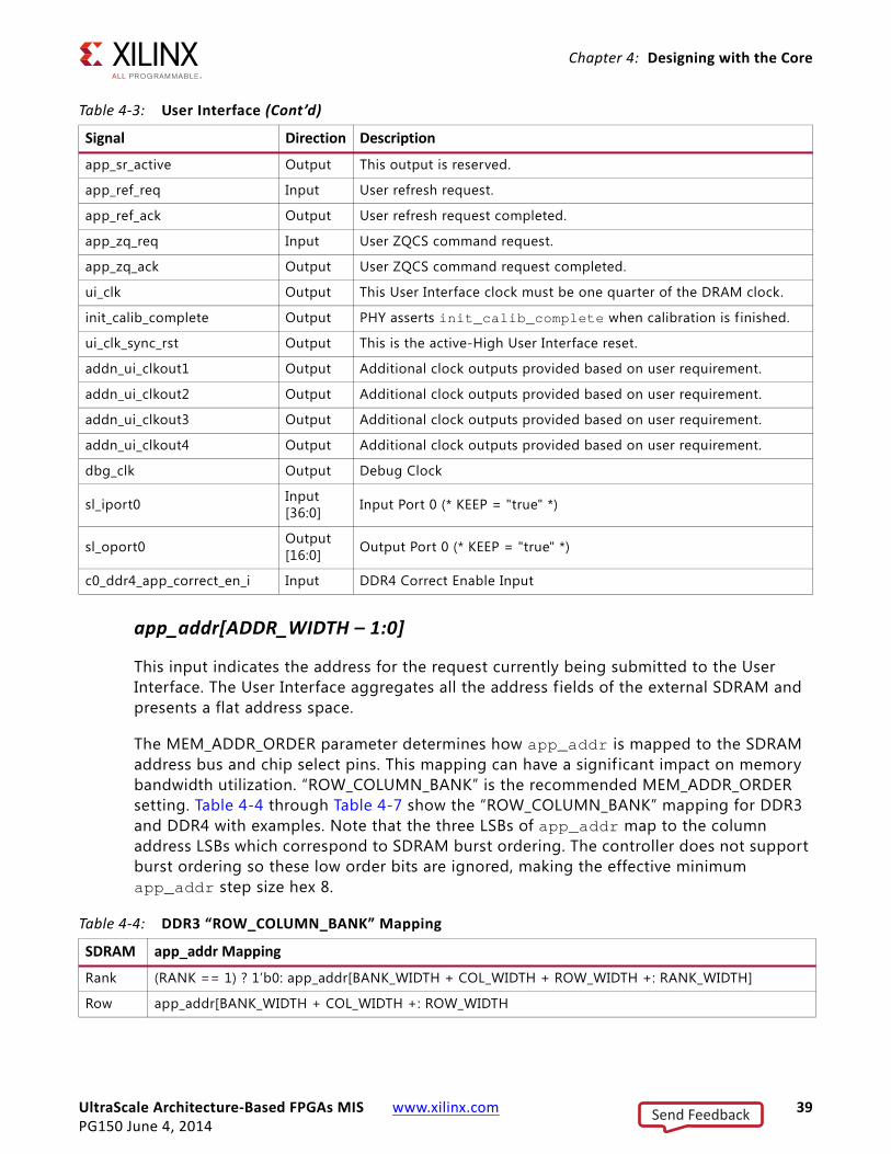
app_addr[ADDR_WIDTH – 1:0]
This input indicates the address for the request currently being submitted to the User Interface. The User Interface aggregates all the address fields of the external SDRAM and presents a flat address space.
The MEM_ADDR_ORDER parameter determines how app_addr is mapped to the SDRAM address bus and chip select pins. This mapping can have a significant impact on memory bandwidth utilization. “ROW_COLUMN_BANK” is the recommended MEM_ADDR_ORDER setting. Table 4-4 through Table 4-7 show the “ROW_COLUMN_BANK” mapping for DDR3 and DDR4 with examples. Note that the three LSBs of app_addr map to the column address LSBs which correspond to SDRAM burst ordering. The controller does not support burst ordering so these low order bits are ignored, making the effective minimum app_addr step size hex 8.
app_sr_active Output This output is reserved.
app_ref_req Input User refresh request.
app_ref_ack Output User refresh request completed.
app_zq_req Input User ZQCS command request.
app_zq_ack Output User ZQCS command request completed.
ui_clk Output This User Interface clock must be one quarter of the DRAM clock.
init_calib_complete Output PHY asserts init_calib_complete when calibration is f inished.
ui_clk_sync_rst Output This is the active-High User Interface reset.
addn_ui_clkout1 Output Additional clock outputs provided based on user requirement.
addn_ui_clkout2 Output Additional clock outputs provided based on user requirement.
addn_ui_clkout3 Output Additional clock outputs provided based on user requirement.
addn_ui_clkout4 Output Additional clock outputs provided based on user requirement.
dbg_clk Output Debug Clock
sl_iport0 Input[36:0] Input Port 0 (* KEEP = "true" *)
sl_oport0 Output[16:0] Output Port 0 (* KEEP = "true" *)
c0_ddr4_app_correct_en_i Input DDR4 Correct Enable Input
Table 4-3: User Interface (Cont’d)
Signal Direction Description
Table 4-4: DDR3 “ROW_COLUMN_BANK” Mapping
SDRAM app_addr Mapping
Rank (RANK == 1) ? 1’b0: app_addr[BANK_WIDTH + COL_WIDTH + ROW_WIDTH +: RANK_WIDTH]
Row app_addr[BANK_WIDTH + COL_WIDTH +: ROW_WIDTH
Send Feedback
UltraScale Architecture-Based FPGAs MIS www.xilinx.com 40PG150 June 4, 2014
Chapter 4: Designing with the Core
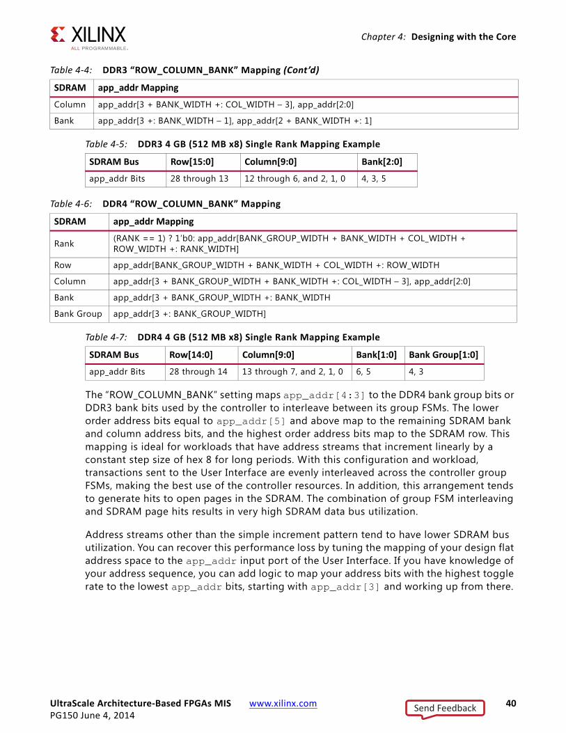
The “ROW_COLUMN_BANK” setting maps app_addr[4:3] to the DDR4 bank group bits or DDR3 bank bits used by the controller to interleave between its group FSMs. The lower order address bits equal to app_addr[5] and above map to the remaining SDRAM bank and column address bits, and the highest order address bits map to the SDRAM row. This mapping is ideal for workloads that have address streams that increment linearly by a constant step size of hex 8 for long periods. With this configuration and workload, transactions sent to the User Interface are evenly interleaved across the controller group FSMs, making the best use of the controller resources. In addition, this arrangement tends to generate hits to open pages in the SDRAM. The combination of group FSM interleaving and SDRAM page hits results in very high SDRAM data bus utilization.
Address streams other than the simple increment pattern tend to have lower SDRAM bus utilization. You can recover this performance loss by tuning the mapping of your design flat address space to the app_addr input port of the User Interface. If you have knowledge of your address sequence, you can add logic to map your address bits with the highest toggle rate to the lowest app_addr bits, starting with app_addr[3] and working up from there.
Column app_addr[3 + BANK_WIDTH +: COL_WIDTH – 3], app_addr[2:0]
Bank app_addr[3 +: BANK_WIDTH – 1], app_addr[2 + BANK_WIDTH +: 1]
Table 4-4: DDR3 “ROW_COLUMN_BANK” Mapping (Cont’d)
SDRAM app_addr Mapping
Table 4-5: DDR3 4 GB (512 MB x8) Single Rank Mapping Example
SDRAM Bus Row[15:0] Column[9:0] Bank[2:0]
app_addr Bits 28 through 13 12 through 6, and 2, 1, 0 4, 3, 5
Table 4-6: DDR4 “ROW_COLUMN_BANK” Mapping
SDRAM app_addr Mapping
Rank (RANK == 1) ? 1’b0: app_addr[BANK_GROUP_WIDTH + BANK_WIDTH + COL_WIDTH + ROW_WIDTH +: RANK_WIDTH]
Row app_addr[BANK_GROUP_WIDTH + BANK_WIDTH + COL_WIDTH +: ROW_WIDTH
Column app_addr[3 + BANK_GROUP_WIDTH + BANK_WIDTH +: COL_WIDTH – 3], app_addr[2:0]
Bank app_addr[3 + BANK_GROUP_WIDTH +: BANK_WIDTH
Bank Group app_addr[3 +: BANK_GROUP_WIDTH]
Table 4-7: DDR4 4 GB (512 MB x8) Single Rank Mapping Example
SDRAM Bus Row[14:0] Column[9:0] Bank[1:0] Bank Group[1:0]
app_addr Bits 28 through 14 13 through 7, and 2, 1, 0 6, 5 4, 3
Send Feedback
UltraScale Architecture-Based FPGAs MIS www.xilinx.com 41PG150 June 4, 2014
Chapter 4: Designing with the Core
For example, if you know that your workload address Bits[4:3] toggle much less than Bits[10:9], which toggle at the highest rate, you could add logic to swap these bits so that your address Bits[10:9] map to app_addr[4:3]. The result is an improvement in how you address stream interleaves across the controller group FSMs, resulting in better controller throughput and higher SDRAM data bus utilization.
app_cmd[2:0]
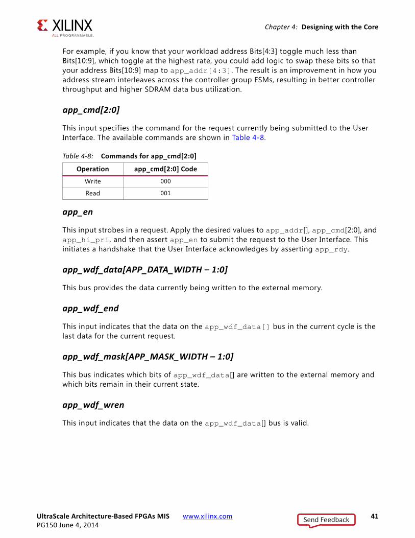
This input specifies the command for the request currently being submitted to the User Interface. The available commands are shown in Table 4-8.
app_en
This input strobes in a request. Apply the desired values to app_addr[], app_cmd[2:0], and app_hi_pri, and then assert app_en to submit the request to the User Interface. This initiates a handshake that the User Interface acknowledges by asserting app_rdy.
app_wdf_data[APP_DATA_WIDTH – 1:0]
This bus provides the data currently being written to the external memory.
app_wdf_end
This input indicates that the data on the app_wdf_data[] bus in the current cycle is the last data for the current request.
app_wdf_mask[APP_MASK_WIDTH – 1:0]
This bus indicates which bits of app_wdf_data[] are written to the external memory and which bits remain in their current state.
app_wdf_wren
This input indicates that the data on the app_wdf_data[] bus is valid.
Table 4-8: Commands for app_cmd[2:0]
Operation app_cmd[2:0] Code
Write 000
Read 001
Send Feedback
UltraScale Architecture-Based FPGAs MIS www.xilinx.com 42PG150 June 4, 2014
Chapter 4: Designing with the Core
app_rdy
This output indicates whether the request currently being submitted to the User Interface is accepted. If the User Interface does not assert this signal after app_en is asserted, the current request must be retried. The app_rdy output is not asserted if:
° PHY/Memory initialization is not yet completed.
° All the bank machines are occupied (can be viewed as the command buffer being full).
- A read is requested and the read buffer is full.
- A write is requested and no write buffer pointers are available.
° A periodic read is being inserted.
app_rd_data[APP_DATA_WIDTH – 1:0]
This output contains the data read from the external memory.
app_rd_data_end
This output indicates that the data on the app_rd_data[] bus in the current cycle is the last data for the current request.
app_rd_data_valid
This output indicates that the data on the app_rd_data[] bus is valid.
app_wdf_rdy
This output indicates that the write data FIFO is ready to receive data. Write data is accepted when both app_wdf_rdy and app_wdf_wren are asserted.
ui_clk_sync_rst
This is the reset from the User Interface which is in synchronous with ui_clk .
ui_clk
This is the output clock from the User Interface. It must be a half or quarter the frequency of the clock going out to the external SDRAM, which depends on 2:1 or 4:1 mode selected in Vivado IDE.
Send Feedback
UltraScale Architecture-Based FPGAs MIS www.xilinx.com 43PG150 June 4, 2014
Chapter 4: Designing with the Core
init_calib_complete
PHY asserts init_calib_complete when calibration is f inished. The application has no need to wait for init_calib_complete before sending commands to the Memory Controller.
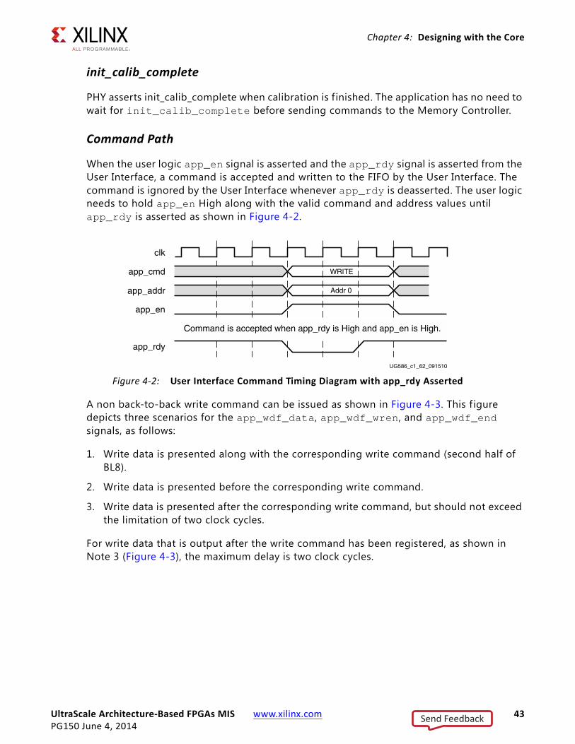
Command Path
When the user logic app_en signal is asserted and the app_rdy signal is asserted from the User Interface, a command is accepted and written to the FIFO by the User Interface. The command is ignored by the User Interface whenever app_rdy is deasserted. The user logic needs to hold app_en High along with the valid command and address values until app_rdy is asserted as shown in Figure 4-2.
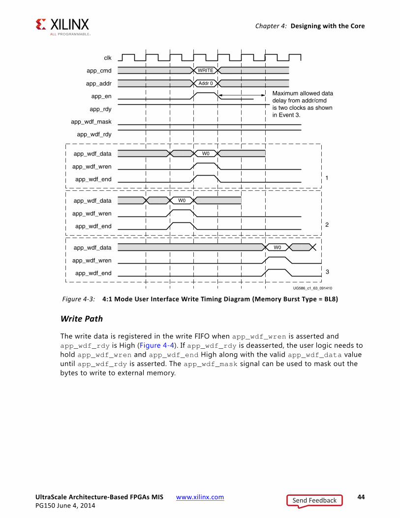
A non back-to-back write command can be issued as shown in Figure 4-3. This f igure depicts three scenarios for the app_wdf_data, app_wdf_wren, and app_wdf_end signals, as follows:
1. Write data is presented along with the corresponding write command (second half of BL8).
2. Write data is presented before the corresponding write command.
3. Write data is presented after the corresponding write command, but should not exceed the limitation of two clock cycles.
For write data that is output after the write command has been registered, as shown in Note 3 (Figure 4-3), the maximum delay is two clock cycles.
X-Ref Target - Figure 4-2
Figure 4-2: User Interface Command Timing Diagram with app_rdy Asserted
Send Feedback
UltraScale Architecture-Based FPGAs MIS www.xilinx.com 44PG150 June 4, 2014
Chapter 4: Designing with the Core
Write Path
The write data is registered in the write FIFO when app_wdf_wren is asserted and app_wdf_rdy is High (Figure 4-4). If app_wdf_rdy is deasserted, the user logic needs to hold app_wdf_wren and app_wdf_end High along with the valid app_wdf_data value until app_wdf_rdy is asserted. The app_wdf_mask signal can be used to mask out the bytes to write to external memory.
X-Ref Target - Figure 4-3
Figure 4-3: 4:1 Mode User Interface Write Timing Diagram (Memory Burst Type = BL8)
Send Feedback
UltraScale Architecture-Based FPGAs MIS www.xilinx.com 45PG150 June 4, 2014
Chapter 4: Designing with the Core
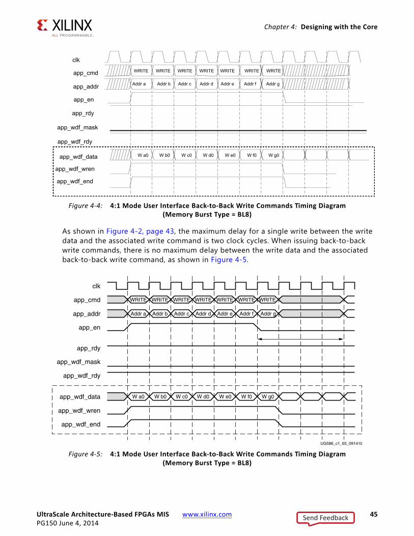
As shown in Figure 4-2, page 43, the maximum delay for a single write between the write data and the associated write command is two clock cycles. When issuing back-to-back write commands, there is no maximum delay between the write data and the associated back-to-back write command, as shown in Figure 4-5.
X-Ref Target - Figure 4-4
Figure 4-4: 4:1 Mode User Interface Back-to-Back Write Commands Timing Diagram (Memory Burst Type = BL8)
X-Ref Target - Figure 4-5
Figure 4-5: 4:1 Mode User Interface Back-to-Back Write Commands Timing Diagram (Memory Burst Type = BL8)
Send Feedback
UltraScale Architecture-Based FPGAs MIS www.xilinx.com 46PG150 June 4, 2014
Chapter 4: Designing with the Core
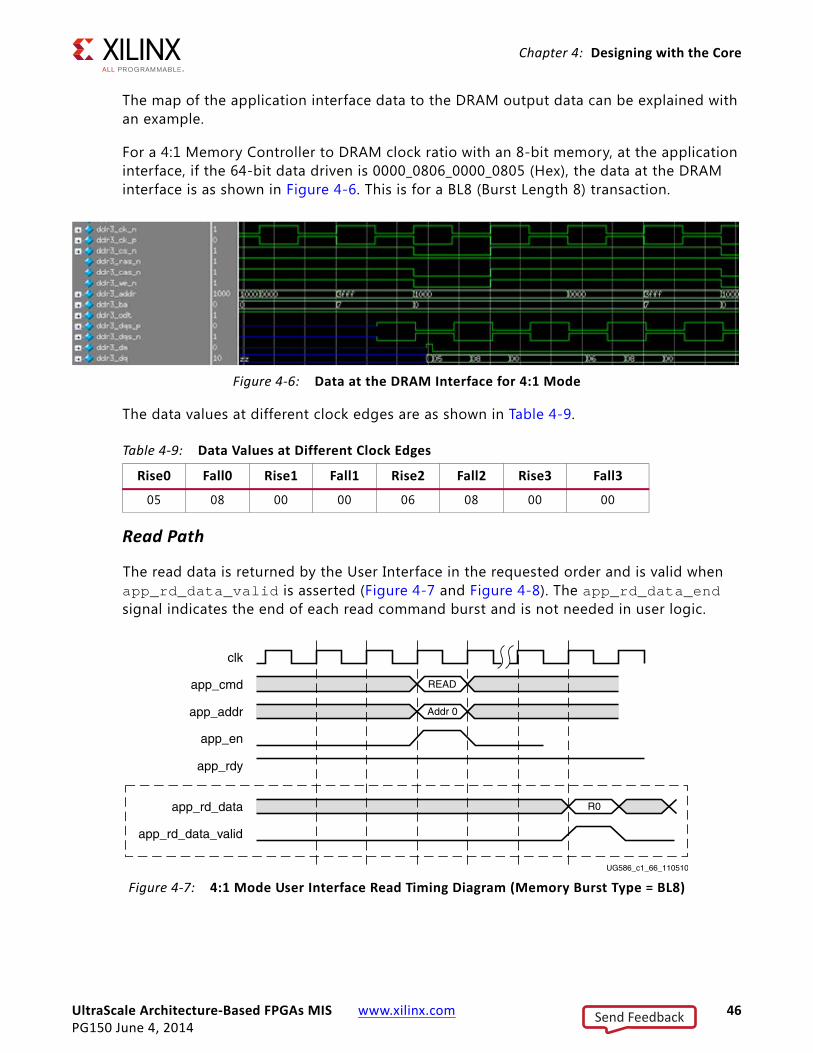
The map of the application interface data to the DRAM output data can be explained with an example.
For a 4:1 Memory Controller to DRAM clock ratio with an 8-bit memory, at the application interface, if the 64-bit data driven is 0000_0806_0000_0805 (Hex), the data at the DRAM interface is as shown in Figure 4-6. This is for a BL8 (Burst Length 8) transaction.
The data values at different clock edges are as shown in Table 4-9.
Read Path
The read data is returned by the User Interface in the requested order and is valid when app_rd_data_valid is asserted (Figure 4-7 and Figure 4-8). The app_rd_data_end signal indicates the end of each read command burst and is not needed in user logic.
X-Ref Target - Figure 4-6
Figure 4-6: Data at the DRAM Interface for 4:1 Mode
Table 4-9: Data Values at Different Clock Edges
Rise0 Fall0 Rise1 Fall1 Rise2 Fall2 Rise3 Fall3
05 08 00 00 06 08 00 00
X-Ref Target - Figure 4-7
Figure 4-7: 4:1 Mode User Interface Read Timing Diagram (Memory Burst Type = BL8)
Send Feedback
UltraScale Architecture-Based FPGAs MIS www.xilinx.com 47PG150 June 4, 2014
Chapter 4: Designing with the Core
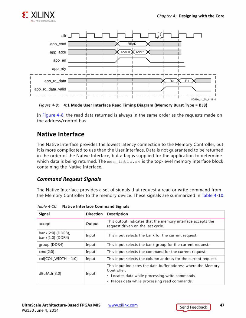
In Figure 4-8, the read data returned is always in the same order as the requests made on the address/control bus.
Native InterfaceThe Native Interface provides the lowest latency connection to the Memory Controller, but it is more complicated to use than the User Interface. Data is not guaranteed to be returned in the order of the Native Interface, but a tag is supplied for the application to determine which data is being returned. The mem_intfc.sv is the top-level memory interface block containing the Native Interface.
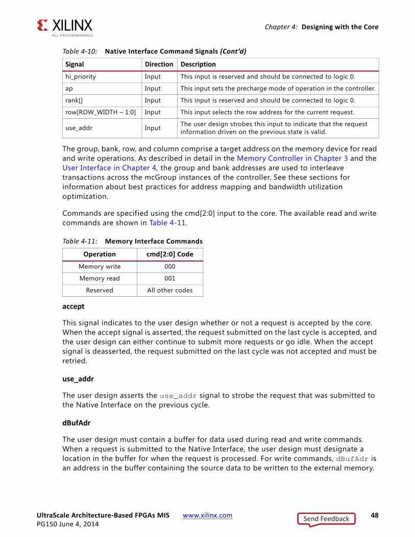
Command Request Signals
The Native Interface provides a set of signals that request a read or write command from the Memory Controller to the memory device. These signals are summarized in Table 4-10.
X-Ref Target - Figure 4-8
Figure 4-8: 4:1 Mode User Interface Read Timing Diagram (Memory Burst Type = BL8)
Table 4-10: Native Interface Command Signals
Signal Direction Description
accept Output This output indicates that the memory interface accepts the request driven on the last cycle.
bank[2:0] (DDR3), bank[1:0] (DDR4) Input This input selects the bank for the current request.
group (DDR4) Input This input selects the bank group for the current request.
cmd[2:0] Input This input selects the command for the current request.
col[COL_WIDTH – 1:0] Input This input selects the column address for the current request.
dBufAdr[3:0] Input
This input indicates the data buffer address where the Memory Controller:• Locates data while processing write commands.• Places data while processing read commands.
Send Feedback
UltraScale Architecture-Based FPGAs MIS www.xilinx.com 48PG150 June 4, 2014
Chapter 4: Designing with the Core
The group, bank, row, and column comprise a target address on the memory device for read and write operations. As described in detail in the Memory Controller in Chapter 3 and the User Interface in Chapter 4, the group and bank addresses are used to interleave transactions across the mcGroup instances of the controller. See these sections for information about best practices for address mapping and bandwidth utilization optimization.
Commands are specif ied using the cmd[2:0] input to the core. The available read and write commands are shown in Table 4-11.
accept
This signal indicates to the user design whether or not a request is accepted by the core. When the accept signal is asserted, the request submitted on the last cycle is accepted, and the user design can either continue to submit more requests or go idle. When the accept signal is deasserted, the request submitted on the last cycle was not accepted and must be retried.
use_addr
The user design asserts the use_addr signal to strobe the request that was submitted to the Native Interface on the previous cycle.
dBufAdr
The user design must contain a buffer for data used during read and write commands. When a request is submitted to the Native Interface, the user design must designate a location in the buffer for when the request is processed. For write commands, dBufAdr is an address in the buffer containing the source data to be written to the external memory.
hi_priority Input This input is reserved and should be connected to logic 0.
ap Input This input sets the precharge mode of operation in the controller.
rank[] Input This input is reserved and should be connected to logic 0.
row[ROW_WIDTH – 1:0] Input This input selects the row address for the current request.
use_addr Input The user design strobes this input to indicate that the request information driven on the previous state is valid.
Table 4-11: Memory Interface Commands
Operation cmd[2:0] Code
Memory write 000
Memory read 001
Reserved All other codes
Table 4-10: Native Interface Command Signals (Cont’d)
Signal Direction Description
Send Feedback
UltraScale Architecture-Based FPGAs MIS www.xilinx.com 49PG150 June 4, 2014
Chapter 4: Designing with the Core
For read commands, dBufAdr is an address in the buffer that receives read data from the external memory. The core echoes this address back when the requests are processed.
ap
The ap signal provides a transaction by transaction control over the auto-precharge feature of the Memory Controller.
There are three modes of operation:
• ap = 0 – The controller behaves in “keep open” mode. Pages are kept open until a different page is opened in the same bank.
• ap = 1 – The controller behaves in “keep closed” mode. This mode is useful for certain special access patterns.
• ap = By Transaction – A page is closed after the transaction if ap = 1 and it is kept open if ap = 0. The user of the Native Interface has transaction by transaction control.
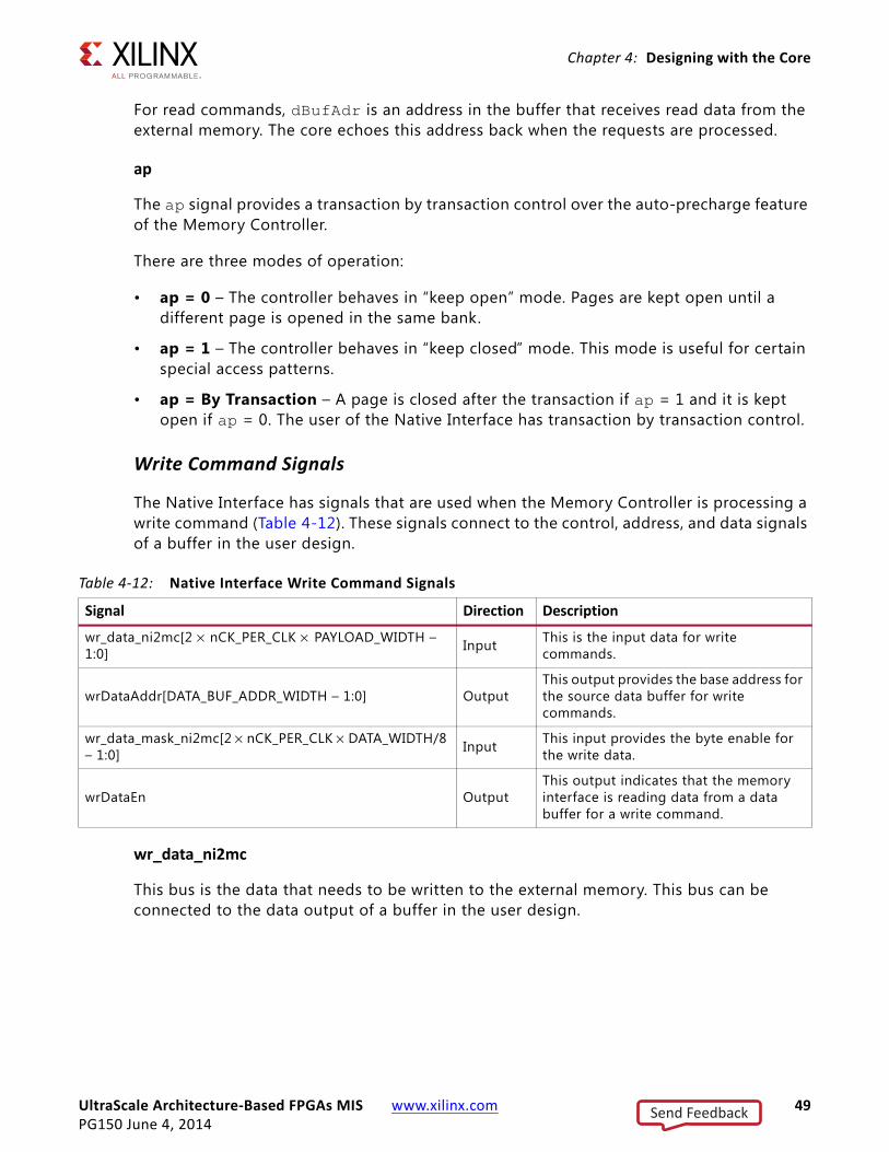
Write Command Signals
The Native Interface has signals that are used when the Memory Controller is processing a write command (Table 4-12). These signals connect to the control, address, and data signals of a buffer in the user design.
wr_data_ni2mc
This bus is the data that needs to be written to the external memory. This bus can be connected to the data output of a buffer in the user design.
Table 4-12: Native Interface Write Command Signals
Signal Direction Description
wr_data_ni2mc[2 × nCK_PER_CLK × PAYLOAD_WIDTH – 1:0] Input This is the input data for write
commands.
wrDataAddr[DATA_BUF_ADDR_WIDTH – 1:0] OutputThis output provides the base address for the source data buffer for write commands.
wr_data_mask_ni2mc[2 × nCK_PER_CLK × DATA_WIDTH/8 – 1:0] Input This input provides the byte enable for
the write data.
wrDataEn OutputThis output indicates that the memory interface is reading data from a data buffer for a write command.
Send Feedback
UltraScale Architecture-Based FPGAs MIS www.xilinx.com 50PG150 June 4, 2014
Chapter 4: Designing with the Core
wrDataAddr
This bus is an echo of dBufAdr. When the controller issues a write CAS on the SDRAM command bus, it outputs the dBufAdr value it received with the write request. The controller expects to receive the write data for the request on the wr_data_ni2mc port on the next clock cycle.
wr_data_mask_ni2mc
This bus is the per byte data mask corresponding to the data on the wr_data_ni2mc bus. The byte to the memory is written when the corresponding wr_data_mask_ni2mc signal is deasserted.
wrDataEn
When asserted, this signal indicates that the controller has requested the write data from buffer location wrDataAddr. This buffer location can be released and used for other transactions.
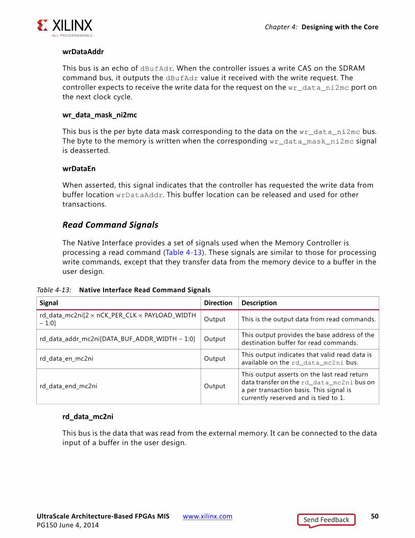
Read Command Signals
The Native Interface provides a set of signals used when the Memory Controller is processing a read command (Table 4-13). These signals are similar to those for processing write commands, except that they transfer data from the memory device to a buffer in the user design.
rd_data_mc2ni
This bus is the data that was read from the external memory. It can be connected to the data input of a buffer in the user design.
Table 4-13: Native Interface Read Command Signals
Signal Direction Description
rd_data_mc2ni[2 × nCK_PER_CLK × PAYLOAD_WIDTH – 1:0] Output This is the output data from read commands.
rd_data_addr_mc2ni[DATA_BUF_ADDR_WIDTH – 1:0] Output This output provides the base address of the destination buffer for read commands.
rd_data_en_mc2ni Output This output indicates that valid read data is available on the rd_data_mc2ni bus.
rd_data_end_mc2ni Output
This output asserts on the last read return data transfer on the rd_data_mc2ni bus on a per transaction basis. This signal is currently reserved and is tied to 1.
Send Feedback
UltraScale Architecture-Based FPGAs MIS www.xilinx.com 51PG150 June 4, 2014
Chapter 4: Designing with the Core
rd_data_addr_mc2ni
When a read request is accepted at the Native Interface, the value of dBufAdr is captured in the controller. The captured value is output on rd_data_addr_mc2ni when read data is returned on rd_data_mc2ni.
rd_data_en_mc2ni
This signal indicates when valid read data is available on rd_data_mc2ni for a read request. It can be tied to the chip select and write enable of a buffer in the user design.
Native Interface Maintenance Command Signals
Table 4-14 lists the Native Interface maintenance command signals.
ref_req
Asserting this signal High for one cycle instructs the controller to halt normal operation and issue one refresh command to each rank. This signal can only be asserted for a single cycle and cannot be asserted again until all outstanding user refresh and user ZQCS requests have been acknowledged. The ref_req signal can be asserted on the same cycle as zq_req to request that both refresh and ZQCS commands are issued to each rank.
The ref_req signal can only be asserted when the controller internal periodic refresh logic is disabled by setting parameter tREFI to 0.
ref_ack
This signal asserts High for a single cycle to acknowledge that a user refresh request has completed.
Table 4-14: Native Interface Maintenance Command Signals
Signal Direction Description
sr_req Input This input is reserved and should be tied to 0.
sr_active Output This output is reserved.
ref_req Input User refresh request.
ref_ack Output User refresh request complete.
zq_req Input User ZQCS command request.
zq_ack Output User ZQCS command request complete.
Send Feedback
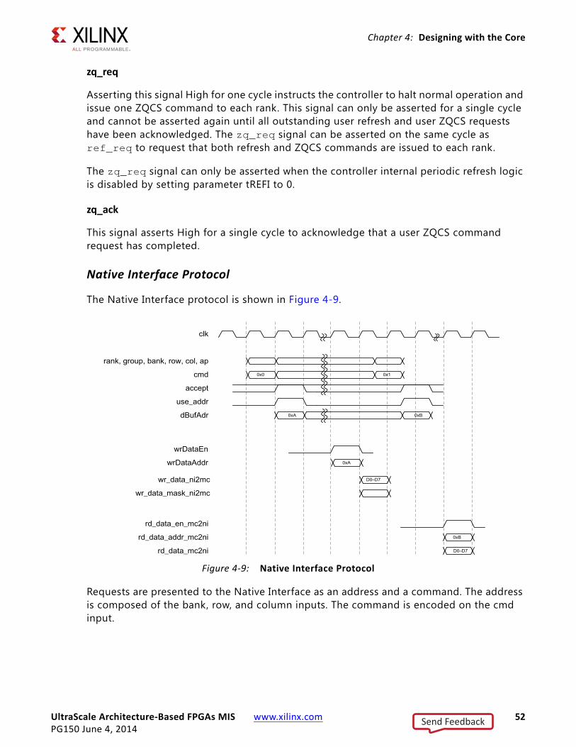
UltraScale Architecture-Based FPGAs MIS www.xilinx.com 52PG150 June 4, 2014
Chapter 4: Designing with the Core
zq_req
Asserting this signal High for one cycle instructs the controller to halt normal operation and issue one ZQCS command to each rank. This signal can only be asserted for a single cycle and cannot be asserted again until all outstanding user refresh and user ZQCS requests have been acknowledged. The zq_req signal can be asserted on the same cycle as ref_req to request that both refresh and ZQCS commands are issued to each rank.
The zq_req signal can only be asserted when the controller internal periodic refresh logic is disabled by setting parameter tREFI to 0.
zq_ack
This signal asserts High for a single cycle to acknowledge that a user ZQCS command request has completed.
Native Interface Protocol
The Native Interface protocol is shown in Figure 4-9.
Requests are presented to the Native Interface as an address and a command. The address is composed of the bank, row, and column inputs. The command is encoded on the cmd input.
X-Ref Target - Figure 4-9
Figure 4-9: Native Interface Protocol
Send Feedback
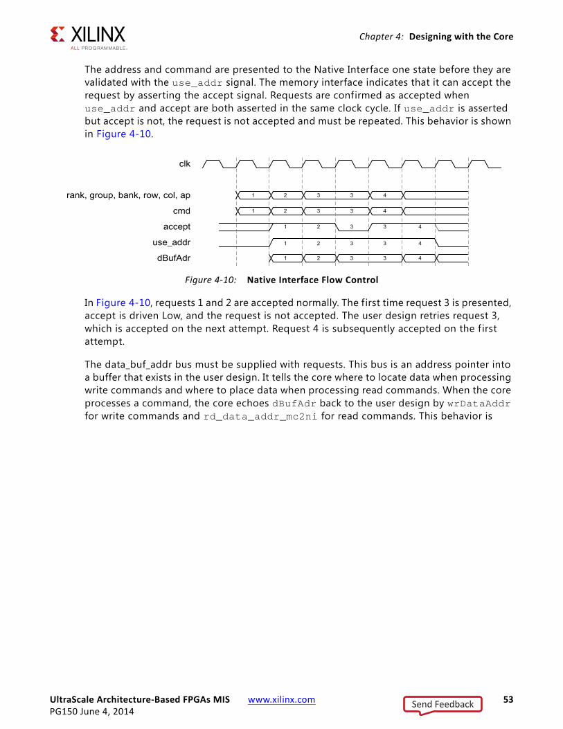
UltraScale Architecture-Based FPGAs MIS www.xilinx.com 53PG150 June 4, 2014
Chapter 4: Designing with the Core
The address and command are presented to the Native Interface one state before they are validated with the use_addr signal. The memory interface indicates that it can accept the request by asserting the accept signal. Requests are confirmed as accepted when use_addr and accept are both asserted in the same clock cycle. If use_addr is asserted but accept is not, the request is not accepted and must be repeated. This behavior is shown in Figure 4-10.
In Figure 4-10, requests 1 and 2 are accepted normally. The first time request 3 is presented, accept is driven Low, and the request is not accepted. The user design retries request 3, which is accepted on the next attempt. Request 4 is subsequently accepted on the f irst attempt.
The data_buf_addr bus must be supplied with requests. This bus is an address pointer into a buffer that exists in the user design. It tells the core where to locate data when processing write commands and where to place data when processing read commands. When the core processes a command, the core echoes dBufAdr back to the user design by wrDataAddr for write commands and rd_data_addr_mc2ni for read commands. This behavior is
X-Ref Target - Figure 4-10
Figure 4-10: Native Interface Flow Control
Send Feedback
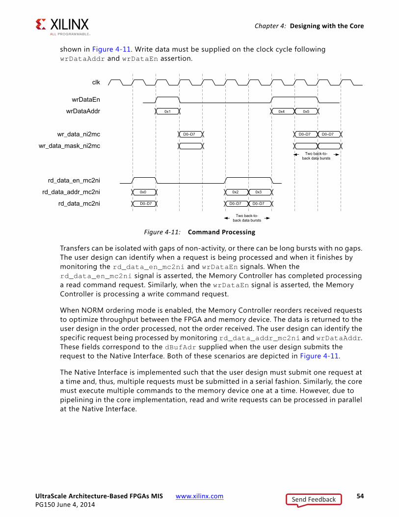
UltraScale Architecture-Based FPGAs MIS www.xilinx.com 54PG150 June 4, 2014
Chapter 4: Designing with the Core
shown in Figure 4-11. Write data must be supplied on the clock cycle following wrDataAddr and wrDataEn assertion.
Transfers can be isolated with gaps of non-activity, or there can be long bursts with no gaps. The user design can identify when a request is being processed and when it f inishes by monitoring the rd_data_en_mc2ni and wrDataEn signals. When the rd_data_en_mc2ni signal is asserted, the Memory Controller has completed processing a read command request. Similarly, when the wrDataEn signal is asserted, the Memory Controller is processing a write command request.
When NORM ordering mode is enabled, the Memory Controller reorders received requests to optimize throughput between the FPGA and memory device. The data is returned to the user design in the order processed, not the order received. The user design can identify the specific request being processed by monitoring rd_data_addr_mc2ni and wrDataAddr. These f ields correspond to the dBufAdr supplied when the user design submits the request to the Native Interface. Both of these scenarios are depicted in Figure 4-11.
The Native Interface is implemented such that the user design must submit one request at a time and, thus, multiple requests must be submitted in a serial fashion. Similarly, the core must execute multiple commands to the memory device one at a time. However, due to pipelining in the core implementation, read and write requests can be processed in parallel at the Native Interface.
X-Ref Target - Figure 4-11
Figure 4-11: Command Processing
Send Feedback
UltraScale Architecture-Based FPGAs MIS www.xilinx.com 55PG150 June 4, 2014
Chapter 5
Design Flow StepsThis chapter describes customizing and generating the core, constraining the core, and the simulation, synthesis and implementation steps that are specific to this IP core. More detailed information about the standard Vivado® design flows in the Vivado IP integrator can be found in the following Vivado Design Suite user guides:
• Vivado Design Suite User Guide: Designing IP Subsystems using IP Integrator (UG994) [Ref 5]
• Vivado Design Suite User Guide: Designing with IP (UG896) [Ref 6]
• Vivado Design Suite User Guide: Getting Started (UG910) [Ref 7]
• Vivado Design Suite User Guide: Logic Simulation (UG900) [Ref 8]
Customizing and Generating the CoreThis section includes information about using Xilinx® tools to customize and generate the core in the Vivado Design Suite.
If you are customizing and generating the core in the IP integrator, see the Vivado Design Suite User Guide: Designing IP Subsystems using IP Integrator (UG994) [Ref 5] for detailed information. IP integrator might auto-compute certain configuration values when validating or generating the design. To check whether the values change, see the description of the parameter in this chapter. To view the parameter value, run the validate_bd_design command in the Tcl Console.
You can customize the IP for use in your design by specifying values for the various parameters associated with the IP core using the following steps:
1. Select the IP from the IP catalog.
2. Double-click the selected IP or select the Customize IP command from the toolbar or right-click menu.
For details, see the Vivado Design Suite User Guide: Designing with IP (UG896) [Ref 6] and the Vivado Design Suite User Guide: Getting Started (UG910) [Ref 7].
Note: Figures in this chapter are illustrations of the Vivado Integrated Design Environment (IDE). This layout might vary from the current version.
Send Feedback
UltraScale Architecture-Based FPGAs MIS www.xilinx.com 56PG150 June 4, 2014
Chapter 5: Design Flow Steps
Controller OptionsFigure 5-1 shows the welcome page when you start up the MIG.
For the Vivado IDE, all controllers (DDR3, DDR4, QDR II+, and RLDRAM 3) can be created and available for instantiation.
In IP integrator, only one controller instance can be created and only two kinds of controllers are available for instantiation:
• DDR3
• DDR4
1. Copy and Delete are not available in the release.
2. After a controller is added with the Add button, click Next and the controller is enabled. DDR4 controller is used for this example (see Figure 5-2),
3. Select the settings in the Clocking, Controller Options, and Memory Options.
X-Ref Target - Figure 5-1
Figure 5-1: Vivado Customize IP Dialog Box – Welcome Page
Send Feedback
UltraScale Architecture-Based FPGAs MIS www.xilinx.com 57PG150 June 4, 2014
Chapter 5: Design Flow Steps
IMPORTANT: Data Mask (DM) option is always selected for AXI designs and is grayed out (you cannot select it). For AXI interfaces, Read Modify Write (RMW) is supported and for RMW to mask certain bytes of Data Mask bits should be present. Therefore, the DM is always enabled for AXI interface designs. This is the case for all data widths except 72-bit. For 72-bit interfaces, ECC is enabled and DM is deselected and grayed out for 72-bit designs. If DM is enabled for 72-bit designs, computing ECC does is not compatible, so DM is disabled for 72-bit designs.
X-Ref Target - Figure 5-2
Figure 5-2: Vivado Customize IP Dialog Box – Controller
Send Feedback
UltraScale Architecture-Based FPGAs MIS www.xilinx.com 58PG150 June 4, 2014
Chapter 5: Design Flow Steps
4. Figure 5-3 shows the next dialog box called Common. This displays the settings for FPGA Options, Debug Signals for Controller, and Clock Options for the specif ic controller.
IMPORTANT: All parameters shown in the controller options dialog box are limited selection options in this release.
MIG I/O PlanningThe MIG I/O planning provides options to modify pin allocation for controllers. It also shows the resource summary of the available I/O ports, allocated I/O ports, and others.
Two methods of performing pin assignment are available:
• Bank Planning
• MIG I/O Pin Planning
X-Ref Target - Figure 5-3
Figure 5-3: Vivado Customize IP Dialog Box – Common
Send Feedback
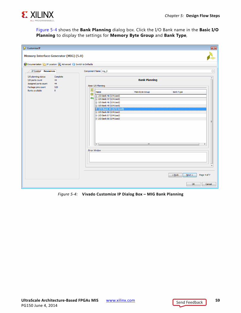
UltraScale Architecture-Based FPGAs MIS www.xilinx.com 59PG150 June 4, 2014
Chapter 5: Design Flow Steps
Figure 5-4 shows the Bank Planning dialog box. Click the I/O Bank name in the Basic I/O Planning to display the settings for Memory Byte Group and Bank Type,
X-Ref Target - Figure 5-4
Figure 5-4: Vivado Customize IP Dialog Box – MIG Bank Planning
Send Feedback
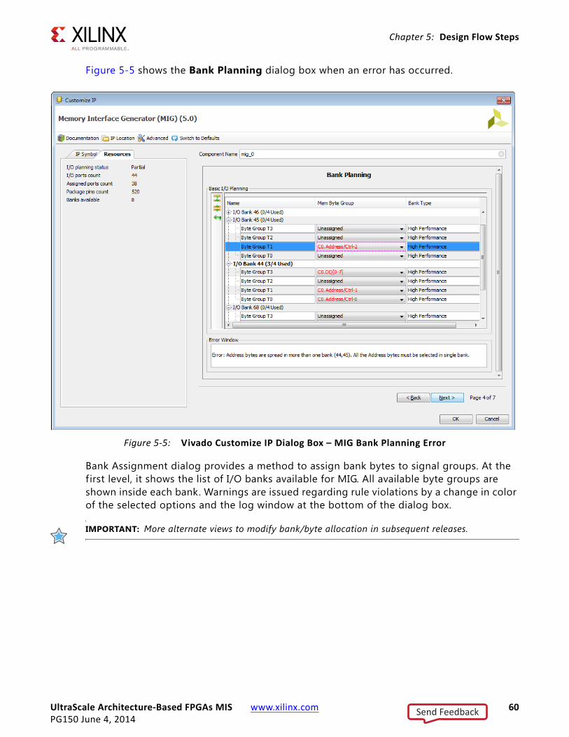
UltraScale Architecture-Based FPGAs MIS www.xilinx.com 60PG150 June 4, 2014
Chapter 5: Design Flow Steps
Figure 5-5 shows the Bank Planning dialog box when an error has occurred.
Bank Assignment dialog provides a method to assign bank bytes to signal groups. At the f irst level, it shows the list of I/O banks available for MIG. All available byte groups are shown inside each bank. Warnings are issued regarding rule violations by a change in color of the selected options and the log window at the bottom of the dialog box.
IMPORTANT: More alternate views to modify bank/byte allocation in subsequent releases.
X-Ref Target - Figure 5-5
Figure 5-5: Vivado Customize IP Dialog Box – MIG Bank Planning Error
Send Feedback
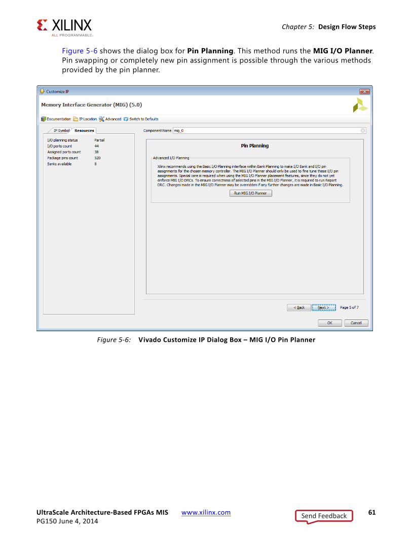
UltraScale Architecture-Based FPGAs MIS www.xilinx.com 61PG150 June 4, 2014
Chapter 5: Design Flow Steps
Figure 5-6 shows the dialog box for Pin Planning. This method runs the MIG I/O Planner. Pin swapping or completely new pin assignment is possible through the various methods provided by the pin planner.
X-Ref Target - Figure 5-6
Figure 5-6: Vivado Customize IP Dialog Box – MIG I/O Pin Planner
Send Feedback
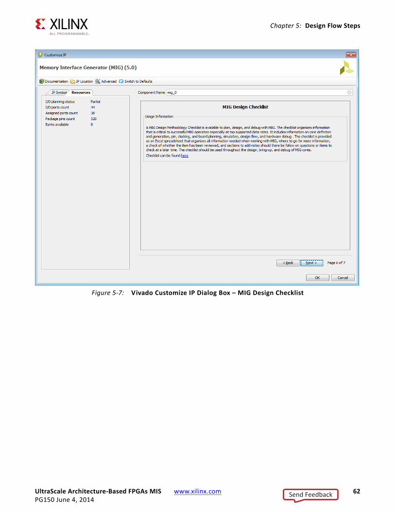
UltraScale Architecture-Based FPGAs MIS www.xilinx.com 62PG150 June 4, 2014
Chapter 5: Design Flow Steps
X-Ref Target - Figure 5-7
Figure 5-7: Vivado Customize IP Dialog Box – MIG Design Checklist
Send Feedback
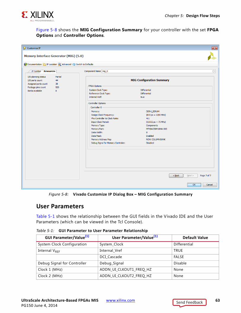
UltraScale Architecture-Based FPGAs MIS www.xilinx.com 63PG150 June 4, 2014
Chapter 5: Design Flow Steps
Figure 5-8 shows the MIG Configuration Summary for your controller with the set FPGA Options and Controller Options.
User ParametersTable 5-1 shows the relationship between the GUI f ields in the Vivado IDE and the User Parameters (which can be viewed in the Tcl Console).
X-Ref Target - Figure 5-8
Figure 5-8: Vivado Customize IP Dialog Box – MIG Configuration Summary
Table 5-1: GUI Parameter to User Parameter RelationshipGUI Parameter/Value(1) User Parameter/Value(1) Default Value
System Clock Configuration System_Clock Differential
Internal VREF Internal_Vref TRUE
DCI_Cascade FALSE
Debug Signal for Controller Debug_Signal Disable
Clock 1 (MHz) ADDN_UI_CLKOUT1_FREQ_HZ None
Clock 2 (MHz) ADDN_UI_CLKOUT2_FREQ_HZ None
Send Feedback
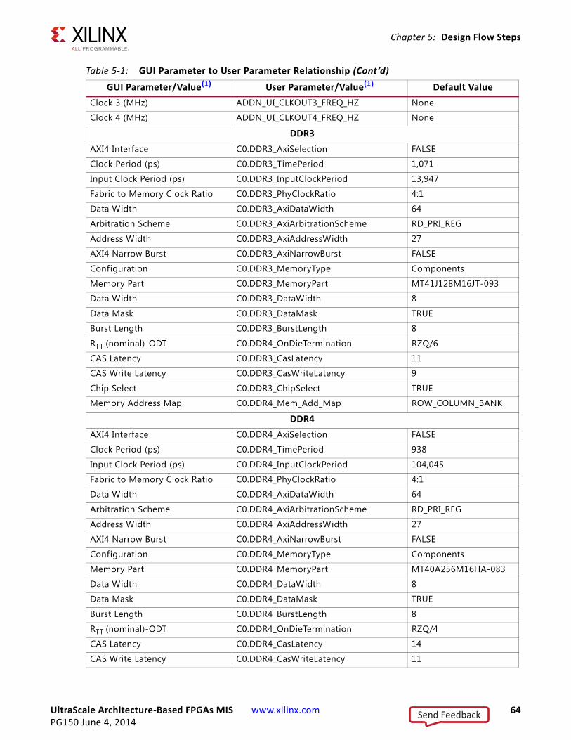
UltraScale Architecture-Based FPGAs MIS www.xilinx.com 64PG150 June 4, 2014
Chapter 5: Design Flow Steps
Clock 3 (MHz) ADDN_UI_CLKOUT3_FREQ_HZ None
Clock 4 (MHz) ADDN_UI_CLKOUT4_FREQ_HZ None
DDR3AXI4 Interface C0.DDR3_AxiSelection FALSE
Clock Period (ps) C0.DDR3_TimePeriod 1,071
Input Clock Period (ps) C0.DDR3_InputClockPeriod 13,947
Fabric to Memory Clock Ratio C0.DDR3_PhyClockRatio 4:1
Data Width C0.DDR3_AxiDataWidth 64
Arbitration Scheme C0.DDR3_AxiArbitrationScheme RD_PRI_REG
Address Width C0.DDR3_AxiAddressWidth 27
AXI4 Narrow Burst C0.DDR3_AxiNarrowBurst FALSE
Configuration C0.DDR3_MemoryType Components
Memory Part C0.DDR3_MemoryPart MT41J128M16JT-093
Data Width C0.DDR3_DataWidth 8
Data Mask C0.DDR3_DataMask TRUE
Burst Length C0.DDR3_BurstLength 8
RTT (nominal)-ODT C0.DDR4_OnDieTermination RZQ/6
CAS Latency C0.DDR3_CasLatency 11
CAS Write Latency C0.DDR3_CasWriteLatency 9
Chip Select C0.DDR3_ChipSelect TRUE
Memory Address Map C0.DDR4_Mem_Add_Map ROW_COLUMN_BANK
DDR4AXI4 Interface C0.DDR4_AxiSelection FALSE
Clock Period (ps) C0.DDR4_TimePeriod 938
Input Clock Period (ps) C0.DDR4_InputClockPeriod 104,045
Fabric to Memory Clock Ratio C0.DDR4_PhyClockRatio 4:1
Data Width C0.DDR4_AxiDataWidth 64
Arbitration Scheme C0.DDR4_AxiArbitrationScheme RD_PRI_REG
Address Width C0.DDR4_AxiAddressWidth 27
AXI4 Narrow Burst C0.DDR4_AxiNarrowBurst FALSE
Configuration C0.DDR4_MemoryType Components
Memory Part C0.DDR4_MemoryPart MT40A256M16HA-083
Data Width C0.DDR4_DataWidth 8
Data Mask C0.DDR4_DataMask TRUE
Burst Length C0.DDR4_BurstLength 8
RTT (nominal)-ODT C0.DDR4_OnDieTermination RZQ/4
CAS Latency C0.DDR4_CasLatency 14
CAS Write Latency C0.DDR4_CasWriteLatency 11
Table 5-1: GUI Parameter to User Parameter Relationship (Cont’d)
GUI Parameter/Value(1) User Parameter/Value(1) Default Value
Send Feedback
UltraScale Architecture-Based FPGAs MIS www.xilinx.com 65PG150 June 4, 2014
Chapter 5: Design Flow Steps
Output GenerationFor details, see the Vivado Design Suite User Guide: Designing with IP (UG896) [Ref 6].
Constraining the CoreThis section contains information about constraining the core in the Vivado Design Suite.
Required ConstraintsThe MIG Vivado IDE generates the required constraints. A location constraint and an I/O standard constraint are added for each external pin in the design. The location is chosen by the Vivado IDE according to the banks and byte lanes chosen for the design.
The I/O standard is chosen by the memory type selection and options in the Vivado IDE and by the pin type. A sample for dq[0] is shown here.
set_property PACKAGE_PIN AF20 [get_ports "c0_ddr4_dq[0]"]set_property IOSTANDARD POD12_DCI [get_ports "c0_ddr4_dq[0]"]
Internal VREF is always used for DDR4. Internal VREF is optional for DDR3. A sample for DDR4 is shown here.
set_property INTERNAL_VREF 0.600 [get_iobanks 45]
Note: The VREF value listed in this constraint is not used. The initial value is set to 0.84V. The calibration logic adjusts this voltage as needed for maximum interface performance.
The system clock must have the period set properly:
create_clock -name c0_sys_clk -period.938 [get_ports c0_sys_clk_p]
IMPORTANT: Do not alter these constraints. If the pin locations need to be altered, rerun the MIG Vivado IDE to generate a new XDC file.
Device, Package, and Speed Grade SelectionsThis section is not applicable for this IP core.
Chip Select C0.DDR4_ChipSelect TRUE
Memory Address Map C0.DDR4_Mem_Add_Map ROW_COLUMN_BANK1. Parameter values are listed in the table where the GUI parameter value differs from the user parameter value. Such
values are shown in this table as indented below the associated parameter.
Table 5-1: GUI Parameter to User Parameter Relationship (Cont’d)
GUI Parameter/Value(1) User Parameter/Value(1) Default Value
Send Feedback
UltraScale Architecture-Based FPGAs MIS www.xilinx.com 66PG150 June 4, 2014
Chapter 5: Design Flow Steps
Clock FrequenciesThis section is not applicable for this IP core.
Clock ManagementFor more information on clocking, see Clocking, page 26.
Clock PlacementThis section is not applicable for this IP core.
BankingThis section is not applicable for this IP core.
Transceiver PlacementThis section is not applicable for this IP core.
I/O Standard and PlacementThe MIG tool generates the appropriate I/O standards and placement based on the selections made in the Vivado IDE for the interface type and options.
IMPORTANT: The set_input_delay and set_output_delay constraints are not needed on the external memory interface pins in this design due to the calibration process that automatically runs at start-up. Warnings seen during implementation for the pins can be ignored.
SimulationThis section contains information about simulating IP in the Vivado Design Suite. For comprehensive information about Vivado simulation components, as well as information about using supported third-party tools, see the Vivado Design Suite User Guide: Logic Simulation (UG900) [Ref 8].
Send Feedback
UltraScale Architecture-Based FPGAs MIS www.xilinx.com 67PG150 June 4, 2014
Chapter 5: Design Flow Steps
Synthesis and ImplementationThis section contains information about synthesis and implementation in the Vivado Design Suite. For details about synthesis and implementation, see the Vivado Design Suite User Guide: Designing with IP (UG896) [Ref 6].
Send Feedback

UltraScale Architecture-Based FPGAs MIS www.xilinx.com 68PG150 June 4, 2014
Chapter 6
Example DesignThis chapter contains information about the example design provided in the Vivado® Design Suite.
Vivado supports Open IP Example Design flow. To create the example design using this flow, right-click the IP in the Source Window, as shown in Figure 6-1 and select Open IP Example Design.
This option creates a new Vivado project. Upon selecting the menu, a dialog box to enter the directory information for the new design project opens.
Select a directory, or use the defaults, and click OK. This launches a new Vivado with all of the example design f iles and a copy of the IP. This project has example_top as the Implementation top directory and sim_tb_top as the Simulation top directory, as shown in Figure 6-2.
X-Ref Target - Figure 6-1
Figure 6-1: Open IP Example Design
Send Feedback

UltraScale Architecture-Based FPGAs MIS www.xilinx.com 69PG150 June 4, 2014
Chapter 6: Example Design
Simulating the Example Design (Designs with Standard User Interface)The example design provides a synthesizable test bench to generate a f ixed simple data pattern to the Memory Controller. This test bench consists of an IP wrapper and an example_tb that generates 10 writes and 10 reads. Memory model f iles are not generated when designs are generated from the IP. You need to download memory models from the Micron® website.
IMPORTANT: Xilinx® UNISIMS_VER and SECUREIP library must be mapped into the simulator.
To run the simulation, go to this directory:
<project_dir>/example_project/<Component_Name>example/<Component_Name>_example.srcs/sim_1/imports/<Component_Name>/tb
X-Ref Target - Figure 6-2
Figure 6-2: Example Design Project
Send Feedback
UltraScale Architecture-Based FPGAs MIS www.xilinx.com 70PG150 June 4, 2014
Chapter 6: Example Design
If the MIG design is generated with the Component Name entered in the Vivado IDE as mig_0, the simulation directory path is the following:
<project_dir>/example_project/mig_0_example/mig_0_example.srcs/sim_1/imports/mig_0/tb
MIG delivers memory models for DDR3 and memory models are not delivered for DDR4. Copy the memory models in the above directory for DDR4. See the readme.txt f ile located in the folder for running simulations.
The Questa® SIM, IES, and VCS simulation tools are used for verif ication of MIG IP at each software release. Script f iles to run simulations with Questa SIM, IES, and VCS are generated in MIG generated output. MIG designs are not verif ied with Vivado Simulator. Other simulation tools can be used for MIG IP simulation but are not specifically verif ied by Xilinx.
Synplify Pro Black Box TestingUsing the Synopsys® Synplify Pro® black box testing for example_design, follow these steps to run black box synthesis with synplify_pro and implementation with Vivado.
1. Generate the UltraScale™ architecture MIG IP core with OOC flow to generate the .dcp f ile for implementation. The Target Language for the project can be selected as verilog or VHDL.
2. Create the example design for the MIG IP core using the information provided in the example design section and close the Vivado project.
3. Invoke the synplify_pro software which supports UltraScale FPGA and select the same UltraScale FPGA part selected at the time of generating the IP core.
4. Add the following files into synplify_pro project based on the Target Language selected at the time of invoking Vivado:
a. For Verilog:
<project_dir>/example_project/<Component_Name>example/<Component_Name>_example.srcs/sources_1/ip/<Component_Name>/*stub.v<project_dir>/example_project/<Component_Name>example/<Component_Name>_example.srcs/sources_1/imports/<Component_Name>/rtl/ip_top/example_top.sv<project_dir>/example_project/<Component_Name>example/<Component_Name>_example.srcs/sources_1/imports/<Component_Name>/tb/example_tb.sv
b. For VHDL:
<project_dir>/example_project/<Component_Name>example/<Component_Name>_example.srcs/sources_1/ip/<Component_Name>/*stub.vhdl <project_dir>/example_project/<Component_Name>example/<Component_Name>_example.srcs/sources_1/imports/<Component_Name>/rtl/ip_top/example_top.sv
Send Feedback

UltraScale Architecture-Based FPGAs MIS www.xilinx.com 71PG150 June 4, 2014
Chapter 6: Example Design
<project_dir>/example_project/<Component_Name>example/<Component_Name>_example.srcs/sources_1/imports/<Component_Name>/tb/example_tb.sv
5. Run synplify_pro synthesis to generate the .edf f ile. Then, close the synplify_pro project.
6. Open new Vivado project with Project Type as Post-synthesis Project and select the Target Language same as selected at the time of generating the IP core.
7. Add the synplify_pro generated .edf f ile to the Vivado project as Design Source.
8. Add the .dcp f ile generated in steps 1 and 2 to the Vivado project as Design Source. For example:
<project_dir>/example_project/<Component_Name>example/<Component_Name>_example.srcs/sources_1/ip/<Component_Name>/<Component_Name>.dcp
9. Add the .xdc f ile generated in step 2 to the Vivado project as constraint. For example:
<project_dir>/example_project/<Component_Name>example/<Component_Name>_example.srcs/constrs_1/imports/par/example_design.xdc
10. Run implementation flow with the Vivado tool. For details about implementation, see the Vivado Design Suite User Guide: Designing with IP (UG896) [Ref 6].
Note: Similar steps can be followed for the user design using appropriate .dcp and .xdc f iles.
Send Feedback
UltraScale Architecture-Based FPGAs MIS www.xilinx.com 72PG150 June 4, 2014
Chapter 7
Test BenchThis chapter contains information about the test bench provided in the Vivado® Design Suite.
The intent of the performance test bench is for you to obtain an estimate on the eff iciency for a given traff ic pattern with the MIG controller. The test bench passes your supplied commands and address to the Memory Controller and measures the eff iciency for the given pattern. The eff iciency is measured by the occupancy of the dq bus. The primary use of the test bench is for efficiency measurements so no data integrity checks are performed. Static data is written into the memory during write transactions and the same data is always read back.
The stimulus to the traff ic generator is provided through a mig_v5_0_ddr4_stimulus.txt f ile. The stimulus consists of command, address, and command repetition count. Each line in the stimulus file represents one stimulus (command repetition, address, and command). Multiple stimuli can be provided in a stimulus f ile and each stimulus is separated by the new line.
Table 7-1: Modules for Performance Traffic Generator
File Name Description
mig_v5_0_ddr4_traff ic_generator.sv This f ile has the traff ic generator code for sending out the traffic for DDR4 and also for the calculation of bus utilized.
mig_v5_0_ddr4_stimulus.txt These files have the stimulus with Writes, Reads, and NOPs for DDR4 for the calculation of bus utilization.
mig_v5_0_ddr3_traff ic_generator.sv This f ile has the traff ic generator code for sending out the traffic for DDR3 and also for the calculation of bus utilized.
mig_v5_0_ddr3_stimulus.txt These files have the stimulus with Writes, Reads, and NOPs for DDR3 for the calculation of bus utilization.
Send Feedback
UltraScale Architecture-Based FPGAs MIS www.xilinx.com 73PG150 June 4, 2014
Chapter 7: Test Bench
Stimulus PatternEach stimulus pattern is 48 bits and the format is described in Table 7-2 and Table 7-3.
Command Encoding (Command[3:0])
Address Encoding (Address[35:0])Address is encoded in the stimulus as per Figure 7-1 to Figure 7-6. All the address f ields need to be entered in the hexadecimal format. All the address fields are the width that is divisible by four to enter in the hexadecimal format. The test bench only sends the required bits of an address field to the Memory Controller.
For example, an eight bank configuration only bank Bits[2:0] is sent to the Memory Controller and the remaining bits are ignored. The extra bits for an address f ield are provided for you to enter the address in a hexadecimal format. You must confirm the value entered corresponds to the width of a given configuration.
• Column Address (Column[11:0]) – Column Address in the stimulus is provided maximum of 12 bits, but you need to address this based on the column width parameter set in your design.
Table 7-2: Stimulus Command Pattern
Command Repeat[47:40] Address [39:4] Command[3:0]
Table 7-3: Stimulus Pattern Description
Signal Description
Command[3:0] This corresponds to the WRITE/READ/NOP command that is sent to the user interface.
Address[35:0] This corresponds to the address to the user interface.
Command Repeat[7:0]This corresponds to the repetition count of the command. Up to 128 repetitions can be made for a command. In the burst length of eight mode, 128 transactions f ill up the page in the memory.
Table 7-4: Command Description
Command Code Description
WRITE 0 This corresponds to the Write operation that needs to be performed.
READ 1 This corresponds to the Read operation that needs to be performed.
NOP 7 This corresponds to the idle situation for the bus.
Table 7-5: Address Encoded
Rank[3:0] Bank[3:0] Row[15:0] Column[11:0]
Send Feedback
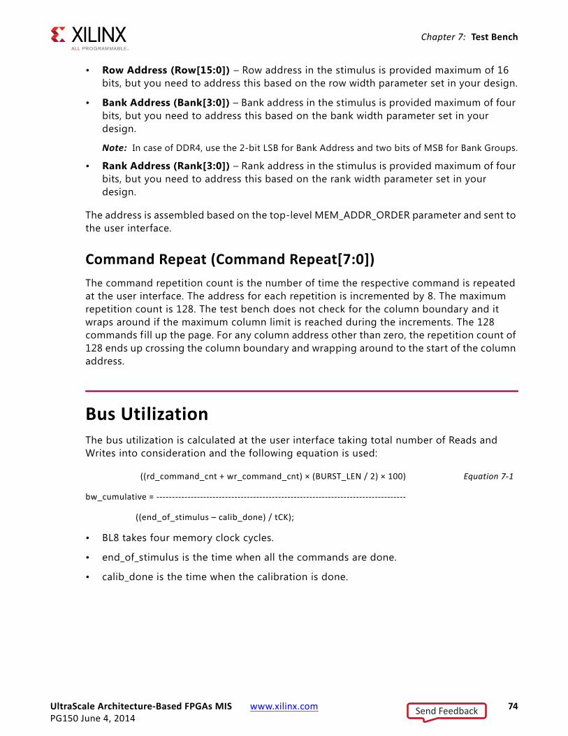
UltraScale Architecture-Based FPGAs MIS www.xilinx.com 74PG150 June 4, 2014
Chapter 7: Test Bench
• Row Address (Row[15:0]) – Row address in the stimulus is provided maximum of 16 bits, but you need to address this based on the row width parameter set in your design.
• Bank Address (Bank[3:0]) – Bank address in the stimulus is provided maximum of four bits, but you need to address this based on the bank width parameter set in your design.
Note: In case of DDR4, use the 2-bit LSB for Bank Address and two bits of MSB for Bank Groups.
• Rank Address (Rank[3:0]) – Rank address in the stimulus is provided maximum of four bits, but you need to address this based on the rank width parameter set in your design.
The address is assembled based on the top-level MEM_ADDR_ORDER parameter and sent to the user interface.
Command Repeat (Command Repeat[7:0])The command repetition count is the number of time the respective command is repeated at the user interface. The address for each repetition is incremented by 8. The maximum repetition count is 128. The test bench does not check for the column boundary and it wraps around if the maximum column limit is reached during the increments. The 128 commands f ill up the page. For any column address other than zero, the repetition count of 128 ends up crossing the column boundary and wrapping around to the start of the column address.
Bus UtilizationThe bus utilization is calculated at the user interface taking total number of Reads and Writes into consideration and the following equation is used:
((rd_command_cnt + wr_command_cnt) × (BURST_LEN / 2) × 100) Equation 7-1
bw_cumulative = --------------------------------------------------------------------------------
((end_of_stimulus – calib_done) / tCK);
• BL8 takes four memory clock cycles.
• end_of_stimulus is the time when all the commands are done.
• calib_done is the time when the calibration is done.
Send Feedback
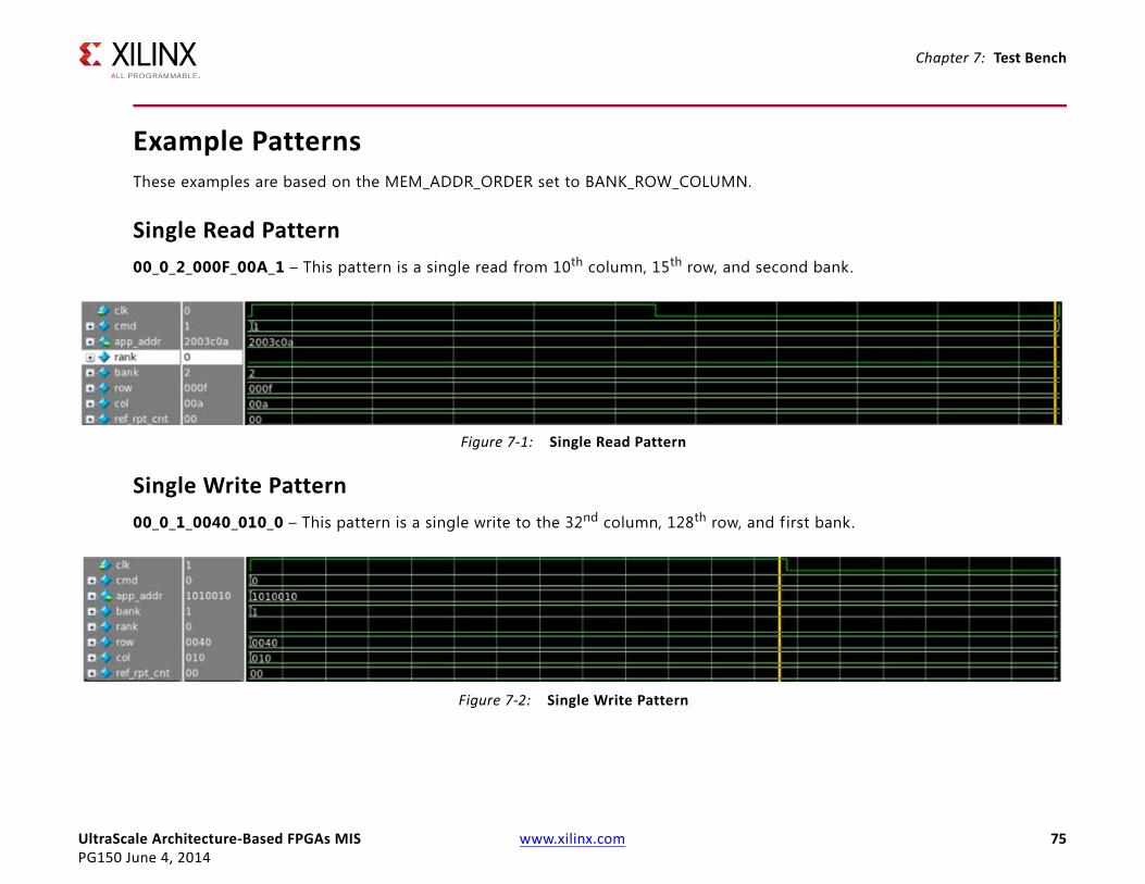
Chapter 7: Test Bench
UltraScale Architecture-Based FPGAs MIS www.xilinx.com 75PG150 June 4, 2014
Example PatternsThese examples are based on the MEM_ADDR_ORDER set to BANK_ROW_COLUMN.
Single Read Pattern00_0_2_000F_00A_1 – This pattern is a single read from 10th column, 15th row, and second bank.
Single Write Pattern00_0_1_0040_010_0 – This pattern is a single write to the 32nd column, 128th row, and f irst bank.
X-Ref Target - Figure 7-1
Figure 7-1: Single Read Pattern
X-Ref Target - Figure 7-2
Figure 7-2: Single Write Pattern
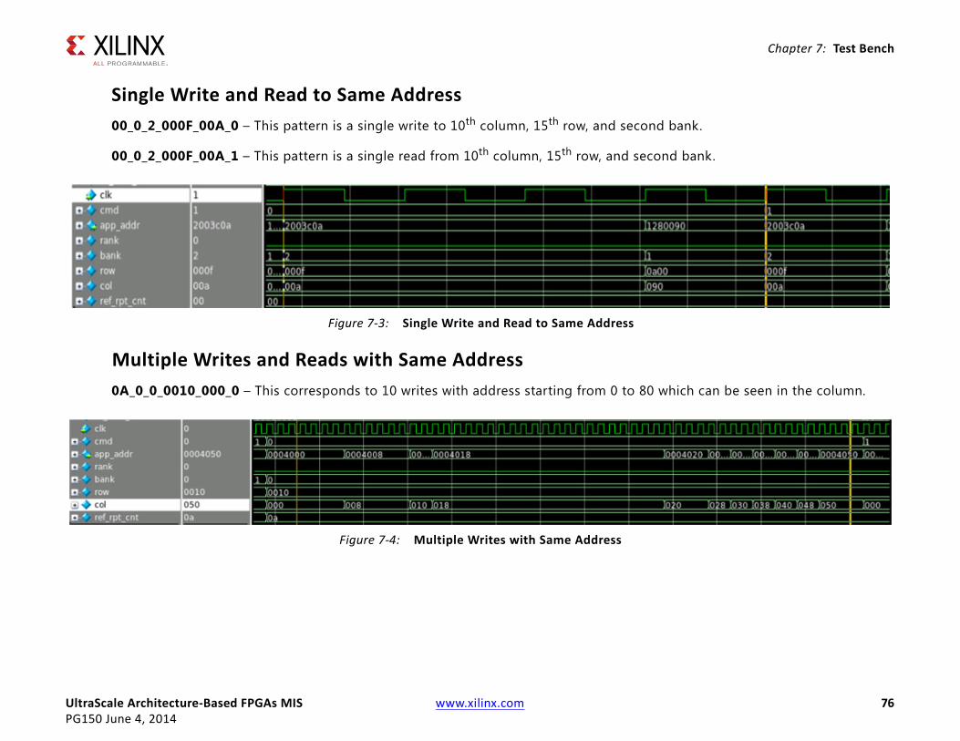
Chapter 7: Test Bench
UltraScale Architecture-Based FPGAs MIS www.xilinx.com 76PG150 June 4, 2014
Single Write and Read to Same Address00_0_2_000F_00A_0 – This pattern is a single write to 10th column, 15th row, and second bank.
00_0_2_000F_00A_1 – This pattern is a single read from 10th column, 15th row, and second bank.
Multiple Writes and Reads with Same Address0A_0_0_0010_000_0 – This corresponds to 10 writes with address starting from 0 to 80 which can be seen in the column.
X-Ref Target - Figure 7-3
Figure 7-3: Single Write and Read to Same Address
X-Ref Target - Figure 7-4
Figure 7-4: Multiple Writes with Same Address
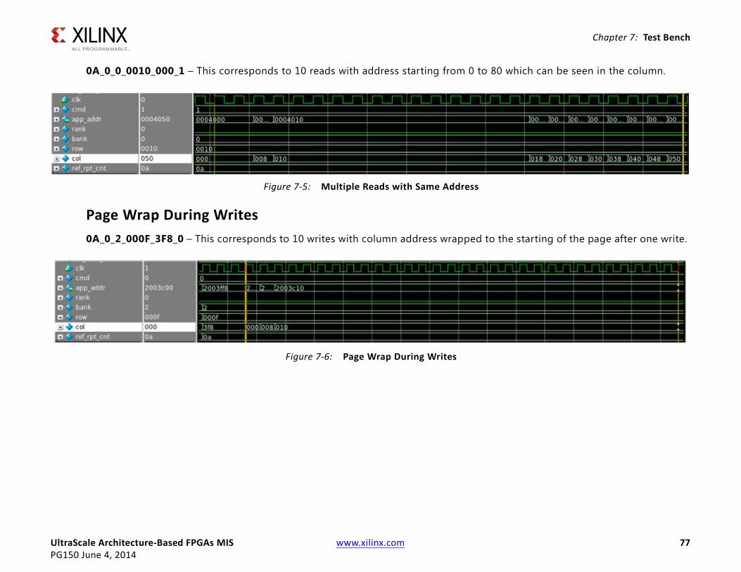
Chapter 7: Test Bench
UltraScale Architecture-Based FPGAs MIS www.xilinx.com 77PG150 June 4, 2014
0A_0_0_0010_000_1 – This corresponds to 10 reads with address starting from 0 to 80 which can be seen in the column.
Page Wrap During Writes0A_0_2_000F_3F8_0 – This corresponds to 10 writes with column address wrapped to the starting of the page after one write.
X-Ref Target - Figure 7-5
Figure 7-5: Multiple Reads with Same Address
X-Ref Target - Figure 7-6
Figure 7-6: Page Wrap During Writes
UltraScale Architecture-Based FPGAs MIS www.xilinx.com 78PG150 June 4, 2014
Chapter 7: Test Bench
Simulating the Performance Traffic Generator1. Map Xilinx® UNISIMS_VER and SECUREIP library into the simulator.
2. MIG delivers memory models for DDR3 and memory models are not delivered for DDR4. Copy the memory models in the following directory for DDR4:
<project_dir>/example_project/<Component_Name>example/<Component_Name>_example.srcs/sim_1/imports/<Component_Name>/tb
3. Modify the mig_v5_0_ddr4_stimulus.txt for DDR4 and mig_v5_0_ddr3_stimulus.txt for DDR3 present in the following directory with the stimulus that wanted the percentage of bus utilization:
<project_dir>/example_project/<Component_Name>example/<Component_Name>_example.srcs/sim_1/imports/<Component_Name>/tb
4. Run the performance_sim.do f ile.
5. For Questa® SIM, run the following command vsim -do performance_sim.do.
6. After the run in the tb directory, mig_v5_0_ddr4_band_width_cal.txt for DDR4 and mig_v5_0_ddr3_band_width_cal.txt for DDR3 are found with all of the output about bus percentage utilization metrics.
Send Feedback
UltraScale Architecture-Based FPGAs MIS www.xilinx.com 79PG150 June 4, 2014
SECTION III: QDR II+ SRAM
Overview
Product Specification
Core Architecture
Designing with the Core
Design Flow Steps
Example Design
Test Bench
Send Feedback
UltraScale Architecture-Based FPGAs MIS www.xilinx.com 80PG150 June 4, 2014
Chapter 8
OverviewThe Xilinx® UltraScale™ architecture includes the QDR II+ SRAM Memory Interface Solutions (MIS) core. This MIS core provides solutions for interfacing with the QDR II+ SRAM memory type.
The QDR II+ SRAM memory interface solution is a physical layer for interfacing Xilinx UltraScale FPGA user designs to the QDR II+ SRAM devices. QDR II+ SRAMs offer high-speed data transfers on separate read and write buses on the rising and falling edges of the clock. These memory devices are used in high-performance systems as temporary data storage, such as:
• Look-up tables in networking systems
• Packet buffers in network switches
• Cache memory in high-speed computing
• Data buffers in high-performance testers
The QDR II+ SRAM solutions core is a PHY that takes simple user commands, converts them to the QDR II+ protocol, and provides the converted commands to the memory. The design enables you to provide one read and one write request per cycle eliminating the need for a Memory Controller and the associated overhead, thereby reducing the latency through the core.
Send Feedback
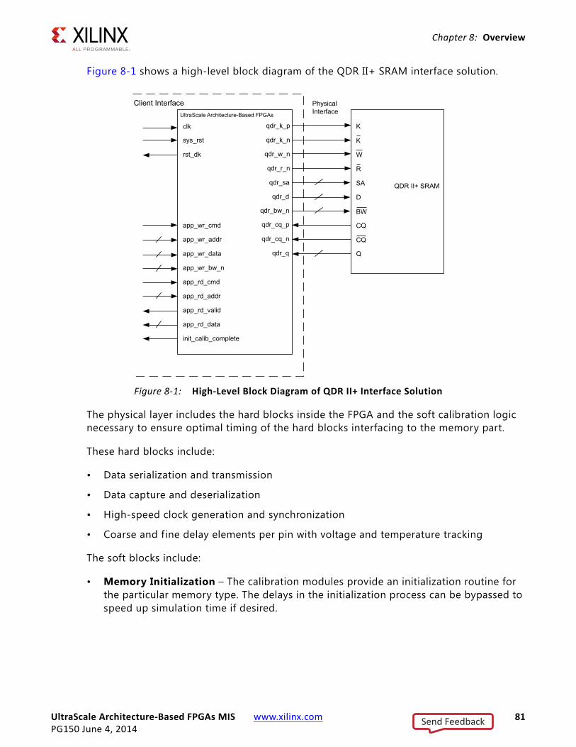
UltraScale Architecture-Based FPGAs MIS www.xilinx.com 81PG150 June 4, 2014
Chapter 8: Overview
Figure 8-1 shows a high-level block diagram of the QDR II+ SRAM interface solution.
The physical layer includes the hard blocks inside the FPGA and the soft calibration logic necessary to ensure optimal timing of the hard blocks interfacing to the memory part.
These hard blocks include:
• Data serialization and transmission
• Data capture and deserialization
• High-speed clock generation and synchronization
• Coarse and fine delay elements per pin with voltage and temperature tracking
The soft blocks include:
• Memory Initialization – The calibration modules provide an initialization routine for the particular memory type. The delays in the initialization process can be bypassed to speed up simulation time if desired.
X-Ref Target - Figure 8-1
Figure 8-1: High-Level Block Diagram of QDR II+ Interface Solution
Send Feedback
UltraScale Architecture-Based FPGAs MIS www.xilinx.com 82PG150 June 4, 2014
Chapter 8: Overview
• Calibration – The calibration modules provide a complete method to set all delays in the hard blocks and soft IP to work with the memory interface. Each bit is individually trained and then combined to ensure optimal interface performance. Results of the calibration process is available through the Xilinx debug tools. After completion of calibration, the PHY layer presents raw interface to the memory part.
Feature Summary• Component support for interface width of 36 bits
• x18 and x36 memory device support
• 4-word and 2-word burst support
• Support for 2.5 cycles of Read Latency
• Source code delivery in Verilog
• 2:1 memory to FPGA logic interface clock ratio
Licensing and Ordering InformationThis Xilinx LogiCORE IP module is provided at no additional cost with the Xilinx Vivado Design Suite under the terms of the Xilinx End User License. Information about this and other Xilinx LogiCORE IP modules is available at the Xilinx Intellectual Property page. For information about pricing and availability of other Xilinx LogiCORE IP modules and tools, contact your local Xilinx sales representative.
License CheckersIf the IP requires a license key, the key must be verif ied. The Vivado® design tools have several license checkpoints for gating licensed IP through the flow. If the license check succeeds, the IP can continue generation. Otherwise, generation halts with error. License checkpoints are enforced by the following tools:
• Vivado design tools: Vivado Synthesis
• Vivado Implementation
• write_bitstream (Tcl command)
IMPORTANT: IP license level is ignored at checkpoints. The test confirms a valid license exists. It does not check IP license level.
Send Feedback
UltraScale Architecture-Based FPGAs MIS www.xilinx.com 83PG150 June 4, 2014
Chapter 9
Product Specification
StandardsThis core complies with the QDR II+ SRAM standard defined by the QDR Consortium. For more information on UltraScale™ architecture documents, see References, page 155.
Performance
Maximum FrequenciesFor more information on the maximum frequencies, see Kintex UltraScale Architecture Data Sheet, DC and AC Switching Characteristics (DS892) [Ref 2].
Resource Utilization
Kintex UltraScale DevicesTable 9-1 provides approximate resource counts on Kintex® UltraScale™ devices.
Resources required for the UltraScale architecture-based FPGAs MIS core have been estimated for the Kintex UltraScale devices. These values were generated using Vivado® IP catalog. They are derived from post-synthesis reports, and might change during implementation.
Table 9-1: Device Utilization – Kintex UltraScale FPGAs
Parameter Values Device Resources
Interface Width FFs LUTs Memory LUTs RAMB36E2/RAMB18E2 BUFGs PLLE3_ADV MMCME3_ADV
36 5,768 4,048 159 20 4 3 1
18 3,974 2,832 159 20 4 2 1
Send Feedback
UltraScale Architecture-Based FPGAs MIS www.xilinx.com 84PG150 June 4, 2014
Chapter 9: Product Specification
Port DescriptionsThere are three port categories at the top-level of the memory interface core called the “user design.”
• The first category is the memory interface signals that directly interfaces with the memory part. These are defined by the QDR II+ SRAM specification.
• The second category is the application interface signals which is referred to as the “user interface.” This is described in the Protocol Description, page 98.
• The third category includes other signals necessary for proper operation of the core. These include the clocks, reset, and status signals from the core. The clocking and reset signals are described in their respective sections.
The active-High init_calib_complete signal indicates that the initialization and calibration are complete and that the interface is now ready to accept commands for the interface.
Send Feedback
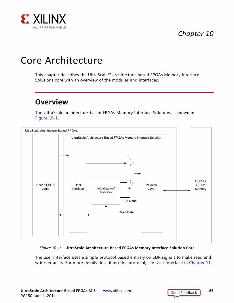
UltraScale Architecture-Based FPGAs MIS www.xilinx.com 85PG150 June 4, 2014
Chapter 10
Core ArchitectureThis chapter describes the UltraScale™ architecture-based FPGAs Memory Interface Solutions core with an overview of the modules and interfaces.
OverviewThe UltraScale architecture-based FPGAs Memory Interface Solutions is shown in Figure 10-1.
The user interface uses a simple protocol based entirely on SDR signals to make read and write requests. For more details describing this protocol, see User Interface in Chapter 11.
X-Ref Target - Figure 10-1
Figure 10-1: UltraScale Architecture-Based FPGAs Memory Interface Solution Core
Send Feedback
UltraScale Architecture-Based FPGAs MIS www.xilinx.com 86PG150 June 4, 2014
Chapter 10: Core Architecture
There is no requirement for controller in QDR II+ SRAM protocol and thus, the Memory Controller contains only the physical interface. It takes commands from the user interface and adheres to the protocol requirements of the QDR II+ SRAM device. It is responsible to generate proper timing relationships and DDR signaling to communicate with the external memory device. For more details, see Physical Interface in Chapter 11.
PHYPHY is considered the low-level physical interface to an external QDR II+ SRAM device. It contains the entire calibration logic for ensuring reliable operation of the physical interface itself. PHY generates the signal timing and sequencing required to interface to the memory device.
PHY contains the following features:
• Clock/address/control-generation logics
• Write and read datapaths
• Logic for initializing the SDRAM after power-up
In addition, PHY contains calibration logic to perform timing training of the read and write datapaths to account for system static and dynamic delays.
Overall PHY ArchitectureThe UltraScale architecture PHY is composed of dedicated blocks and soft calibration logic. The dedicated blocks are structured adjacent to one another with back-to-back interconnects to minimize the clock and datapath routing necessary to build high performance physical layers.
Send Feedback
UltraScale Architecture-Based FPGAs MIS www.xilinx.com 87PG150 June 4, 2014
Chapter 10: Core Architecture
The user interface and calibration logic communicate with this dedicated PHY in the slow frequency clock domain, which is divided by 2. A more detailed block diagram of the PHY design is shown in Figure 10-2.
X-Ref Target - Figure 10-2
Figure 10-2: PHY Block Diagram
Table 10-1: PHY Modules
Module Name Description
qdriip_phy.sv PHY top of QDR II+ design
qdriip_phycal.sv Contains the instances of XIPHY top and calibration top modules
qdriip_cal.sv Calibration top module
qdriip_cal_addr_decode.sv FPGA logic interface for the MicroBlaze processor
config_rom.sv Configuration storage for calibration options
debug_microblaze.sv MicroBlaze processor
qdriip_xiphy.sv Contains the XIPHY instance
qdriip_iob.sv Instantiates all byte IOB modules
qdriip_iob_byte.sv Generates the I/O buffers for all the signals in a given byte lane
qdriip_rd_bit_slip.sv Read bit slip
Send Feedback
UltraScale Architecture-Based FPGAs MIS www.xilinx.com 88PG150 June 4, 2014
Chapter 10: Core Architecture
The PHY architecture encompasses all of the logic contained in qdriip_xiphy.sv. The PHY contains wrappers around dedicated hard blocks to build up the memory interface from smaller components. A byte lane contains all of the clocks, resets, and datapaths for a given subset of I/O. Multiple byte lanes are grouped together, along with dedicated clocking resources, to make up a single bank memory interface. For more information on the hard silicon physical layer architecture, see the UltraScale™ Architecture-Based FPGAs SelectIO™ Resources User Guide (UG571) [Ref 3].
The memory initialization and calibration are implemented in C programming on a small soft core processor. The MicroBlaze™ Controller System (MCS) is configured with an I/O Module and block RAM. The module qdriip_cal_adr_decode.sv module provides the interface for the processor to the rest of the system and implements helper logic. The config_rom.sv module stores settings that control the operation of initialization and calibration, providing run time options that can be adjusted without having to recompile the source code.
The address unit connects the MCS to the local register set and the PHY by performing address decode and control translation on the I/O module bus from spaces in the memory map and MUXing return data (qdriip_cal_adr_decode.sv). In addition, it provides address translation (also known as “mapping”) from a logical conceptualization of the DRAM interface to the appropriate pinout-dependent location of the delay control in the PHY address space.
Although the calibration architecture presents a simple and organized address map for manipulating the delay elements for individual data, control and command bits, there is flexibility in how those I/O pins are placed. For a given I/O placement, the path to the FPGA logic is locked to a given pin. To enable a single binary software f ile to work with any memory interface pinout, a translation block converts the simplif ied RIU addressing into the pinout-specific RIU address for the target design. The specif ic address translation is written by MIG after a pinout is selected. The code shows an example of the RTL structure that supports this.
Casez(io_address)// MicroBlaze I/O module address // … static address decoding skipped //========================================// //===========DQ ODELAYS===================// //========================================// //Byte0 28’h0004100: begin //dq2 riu_addr_cal = /* MIG Generated */ 6’hd; riu_nibble = /* MIG Generated */ ‘h0; end // … additional dynamic addressing follows
In this example, DQ0 is pinned out on Bit[0] of nibble 0 (nibble 0 according to instantiation order). The RIU address for the ODELAY for Bit[0] is 0x0D (for more details on the RIU address map, see the RIU specification). When DQ0 is addressed — indicated by address 0x000_4100), this snippet of code is active. It enables nibble 0 (decoded to one-hot downstream) and forwards the address 0x0D to the RIU address bus.
Send Feedback
UltraScale Architecture-Based FPGAs MIS www.xilinx.com 89PG150 June 4, 2014
Chapter 10: Core Architecture
The MicroBlaze I/O module interface updates at a maximum rate of once every three clock cycles, which is not always fast enough for implementing all of the functions required in calibration. A helper circuit implemented in qdriip_cal_adr_decode.sv is required to obtain commands from the registers and translate at least a portion into single-cycle accuracy for submission to the PHY. In addition, it supports command repetition to enable back-to-back read transactions and read data comparison.
Memory Initialization and Calibration SequenceAfter deassertion of the system reset, PHY performs some required internal calibration steps first.
1. The built-in self-check of the PHY (BISC) is run.
2. BISC is used in the PHY to compensate internal skews among the data bits and the strobe on the read path. The computed skews are used in the voltage and temperature tracking after calibration is completed.
3. After BISC is completed, calibration logic performs the required power-on initialization sequence for the memory. This is followed by several stages of timing calibration for the write and read datapaths.
4. After calibration is completed, PHY calculates internal offsets to be used in voltage and temperature tracking.
5. When PHY indicates the calibration completion, the user interface commands execution begins.
Send Feedback
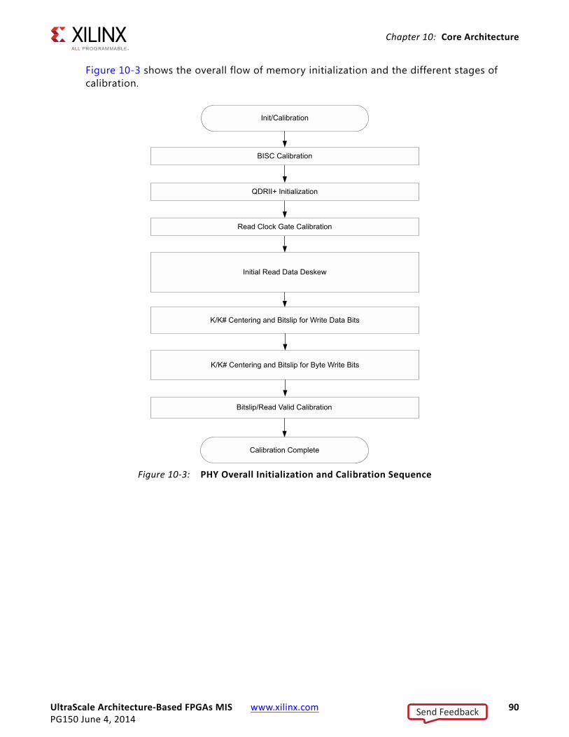
UltraScale Architecture-Based FPGAs MIS www.xilinx.com 90PG150 June 4, 2014
Chapter 10: Core Architecture
Figure 10-3 shows the overall flow of memory initialization and the different stages of calibration.
X-Ref Target - Figure 10-3
Figure 10-3: PHY Overall Initialization and Calibration Sequence
Send Feedback

UltraScale Architecture-Based FPGAs MIS www.xilinx.com 91PG150 June 4, 2014
Chapter 11
Designing with the CoreThis chapter includes guidelines and additional information to facilitate designing with the core.
ClockingThe memory interface requires one MMCM, one TXPLL per I/O bank used by the memory interface, two BUFGs, and one BUFGCE_DIV. These clocking components are used to create the proper clock frequencies and phase shifts necessary for the proper operation of the memory interface.
There are two TXPLLs per bank. If a bank is shared by two memory interfaces, both TXPLLs in that bank are used.
Note: MIG generates the appropriate clocking structure and no modifications to the RTL are supported.
The MIG tool generates the appropriate clocking structure for the desired interface. This structure must not be modif ied. The allowed clock configuration is as follows:
• Differential reference clock source connected to GCIO
• GCIO to MMCM (located in same bank as GCIO)
• MMCM to BUFG (located in same bank as MMCM)
• BUFG (at MMCM) to BUFG (located at center bank of memory interface) driving FPGA logic and all TXPLLs
• BUFG (at MMCM) to BUFGCE_DIV (located at center bank of memory interface) divide by two mode driving 1/2 rate FPGA logic
• Clocking pair of the interface must be in the same SLR of memory interface for the SSI technology devices
Send Feedback
UltraScale Architecture-Based FPGAs MIS www.xilinx.com 92PG150 June 4, 2014
Chapter 11: Designing with the Core
Requirements
GCIO
• Must use a differential I/O standard
• Must be in the same I/O column as the memory interface
MMCM
• MMCM is used to generate the FPGA logic system clock (1/4 of the memory clock)
• Must be located in the same bank as the GCIO
• Must use internal feedback
• Input clock frequency divided by input divider must be ≥ 70 MHz (CLKINx / D ≥ 70 MHz)
• Must use integer multiply and output divide values
BUFG and Clock Root at MMCM
• Must be placed in the same bank as the MMCM
BUFG/BUFGCE_DIV and Clock Roots
• BUFGCE_DIV is used to divide the system clock by two.
• BUFGCE_DIV and BUFG and clock roots must be located in center most bank of the memory interface.
° For two bank systems, either bank can be used. MIG is always referred to the top-most selected bank in the GUI as the center bank.
° For four bank systems, either of the center banks can be chosen. MIG refers to the second bank from the top-most selected bank as the center bank.
° BUFG and BUFGCE_DIV must be in the same bank.
TXPLL
• CLKOUTPHY from TXPLL drives XiPhy within its bank
• TXPLL must be set to use a CLKFBOUT phase shift of 90°
• TXPLL must be held in reset until the MMCM lock output goes High
• Must use internal feedback
Send Feedback
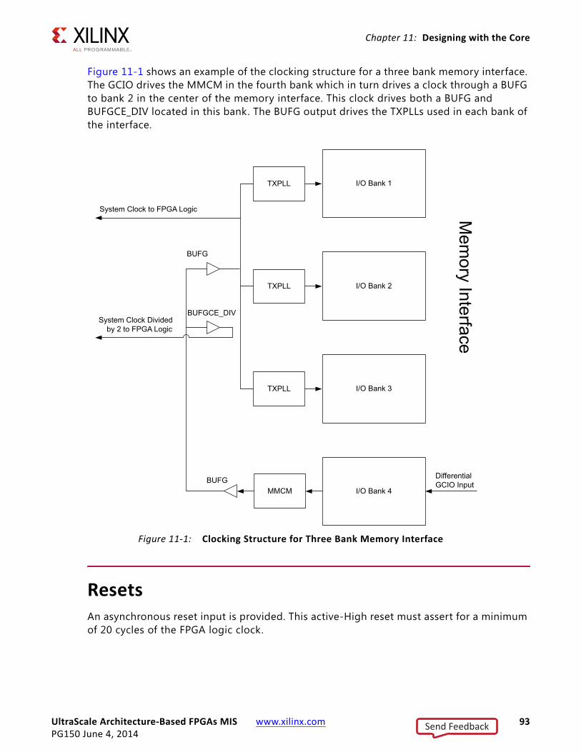
UltraScale Architecture-Based FPGAs MIS www.xilinx.com 93PG150 June 4, 2014
Chapter 11: Designing with the Core
Figure 11-1 shows an example of the clocking structure for a three bank memory interface. The GCIO drives the MMCM in the fourth bank which in turn drives a clock through a BUFG to bank 2 in the center of the memory interface. This clock drives both a BUFG and BUFGCE_DIV located in this bank. The BUFG output drives the TXPLLs used in each bank of the interface.
ResetsAn asynchronous reset input is provided. This active-High reset must assert for a minimum of 20 cycles of the FPGA logic clock.
X-Ref Target - Figure 11-1
Figure 11-1: Clocking Structure for Three Bank Memory Interface
Send Feedback
UltraScale Architecture-Based FPGAs MIS www.xilinx.com 94PG150 June 4, 2014
Chapter 11: Designing with the Core
PCB Guidelines for QDR II+ SRAMStrict adherence to all documented QDR II+ SRAM PCB guidelines is required for successful operation. For more information on PCB guidelines, see the UltraScale Architecture PCB Design and Pin Planning User Guide (UG583) [Ref 4].
Pin and Bank Rules
QDR II+ Pin RulesThis section describes the pin out rules for QDR II+ SRAM interface.
• Both HR and HP Banks are supported.
• All signal groups that are write data, read data, address/control, and system clock interfaces must be selected in a single column.
• All banks used must be adjacent. No skip banks allowed.
1. Write Data (D) and Byte Write (BW) Pins Allocation:
a. The entire write data bus must be placed in a single bank regardless of the number of memory components.
b. Only one write data byte is allowed per byte lane.
c. All byte lanes that are used for the write data of a single component must be adjacent, no skip byte lanes are allowed.
d. One of the write data bytes of a memory component should be allocated in the center byte lanes (byte lanes 1 and 2).
e. Each byte write pin (BW) must be allocated in the corresponding write data byte lane.
2. Memory Clock (K/K#) Allocation:
a. Memory Clock pair must be allocated in one of the byte lanes that are used for the write data of the corresponding memory component.
b. Memory clock should come from one of the center byte lanes (byte lanes 1 and 2).
c. K/K# can be allocated to any PN pair.
3. Read Data (Q) Allocation:
a. The entire read data bus must be placed in a single bank irrespective of the number of memory components.
Send Feedback
UltraScale Architecture-Based FPGAs MIS www.xilinx.com 95PG150 June 4, 2014
Chapter 11: Designing with the Core
b. All byte lanes that are used for the read data of a single component must be adjacent, no skip byte lanes are allowed.
c. One of the read data bytes of a memory component should be allocated in the center byte lanes (byte lanes 1 and 2).
d. If a byte lane is used for read data, Bit[0] and Bit[6] must be used. Read clock (CQ or CQ#) gets the f irst priority and data (Q) is the next.
e. Read data buses of two components should not share a byte lane.
4. Read Clock (CQ/CQ#) Allocation:
a. Read Clock pair must be allocated in one of the byte lanes that are used for the read data of the corresponding memory component.
b. CQ/CQ# pair must be allocated in a single byte lane.
c. CQ/CQ# must be allocated only in the center byte lanes (byte lanes 1 and 2) because other byte lanes cannot forward the clock out for read data capture.
d. CQ and CQ# must be allocated to either pin 0 or pin 6 of a byte lane. For example, if CQ is allocated to pin 0, CQ# should be allocated to pin 6 and vice versa.
5. Address/Control (A/C) Pins Allocation:
a. All address/control (A/C) bits must be allocated in a single bank.
b. All A/C byte lanes should be contiguous and no skip byte lanes is allowed.
c. The address/control bank should be the same or adjacent to that of the write data bank.
d. There should not be any empty byte lane or read byte lane between A/C and write data byte lanes. This rule applies when A/C and write data share the same bank or allocated in adjacent banks.
e. Address/control pins should not share a byte lane with the write data as well as read data.
f. System clock pins (sys_clk_p/sys_clk_n) must be placed on any GCCIO pin pair in the same column as that of the memory interface.
6. All I/O banks used by the memory interface must be in the same SLR of the column for the SSI technology devices.
QDR II+ Pinout Examples
IMPORTANT: Due to the calibration stage, there is no need for set_input_delay/set_output_delay on the MIG. You need to ignore the unconstrained inputs and outputs for MIG and the signals which are calibrated.
Send Feedback
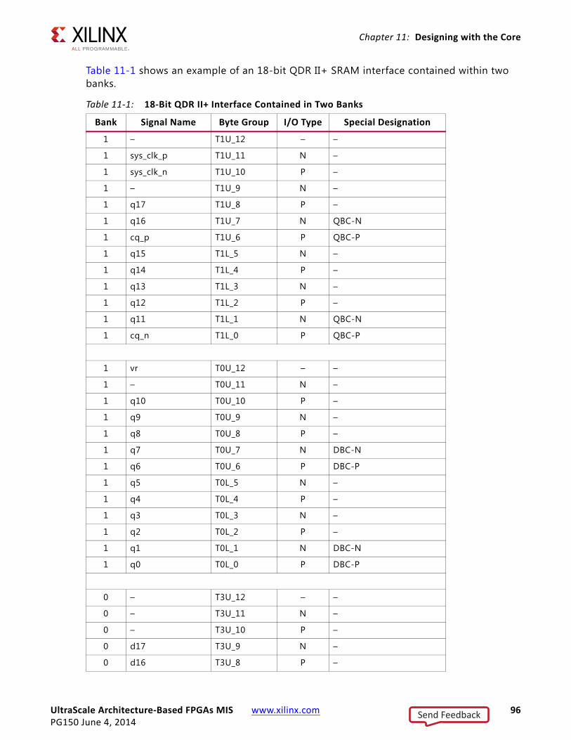
UltraScale Architecture-Based FPGAs MIS www.xilinx.com 96PG150 June 4, 2014
Chapter 11: Designing with the Core
Table 11-1 shows an example of an 18-bit QDR II+ SRAM interface contained within two banks.
Table 11-1: 18-Bit QDR II+ Interface Contained in Two Banks
Bank Signal Name Byte Group I/O Type Special Designation
1 – T1U_12 – –
1 sys_clk_p T1U_11 N –
1 sys_clk_n T1U_10 P –
1 – T1U_9 N –
1 q17 T1U_8 P –
1 q16 T1U_7 N QBC-N
1 cq_p T1U_6 P QBC-P
1 q15 T1L_5 N –
1 q14 T1L_4 P –
1 q13 T1L_3 N –
1 q12 T1L_2 P –
1 q11 T1L_1 N QBC-N
1 cq_n T1L_0 P QBC-P
1 vr T0U_12 – –
1 – T0U_11 N –
1 q10 T0U_10 P –
1 q9 T0U_9 N –
1 q8 T0U_8 P –
1 q7 T0U_7 N DBC-N
1 q6 T0U_6 P DBC-P
1 q5 T0L_5 N –
1 q4 T0L_4 P –
1 q3 T0L_3 N –
1 q2 T0L_2 P –
1 q1 T0L_1 N DBC-N
1 q0 T0L_0 P DBC-P
0 – T3U_12 – –
0 – T3U_11 N –
0 – T3U_10 P –
0 d17 T3U_9 N –
0 d16 T3U_8 P –
Send Feedback
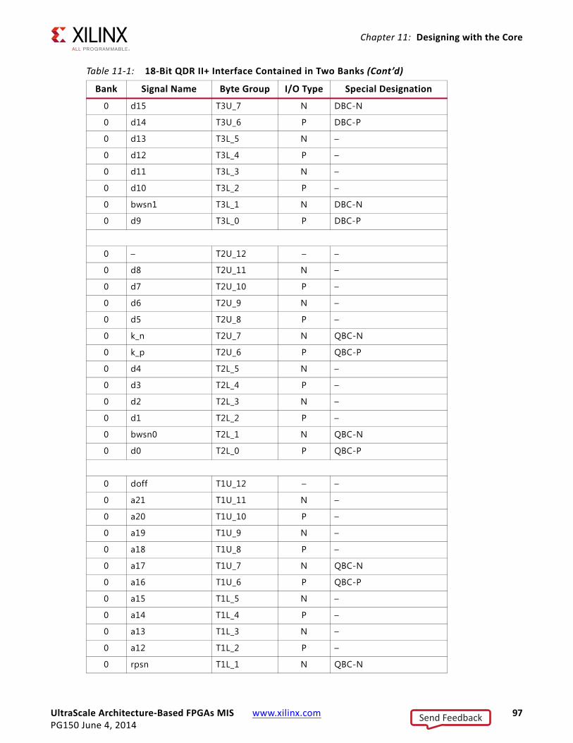
UltraScale Architecture-Based FPGAs MIS www.xilinx.com 97PG150 June 4, 2014
Chapter 11: Designing with the Core
0 d15 T3U_7 N DBC-N
0 d14 T3U_6 P DBC-P
0 d13 T3L_5 N –
0 d12 T3L_4 P –
0 d11 T3L_3 N –
0 d10 T3L_2 P –
0 bwsn1 T3L_1 N DBC-N
0 d9 T3L_0 P DBC-P
0 – T2U_12 – –
0 d8 T2U_11 N –
0 d7 T2U_10 P –
0 d6 T2U_9 N –
0 d5 T2U_8 P –
0 k_n T2U_7 N QBC-N
0 k_p T2U_6 P QBC-P
0 d4 T2L_5 N –
0 d3 T2L_4 P –
0 d2 T2L_3 N –
0 d1 T2L_2 P –
0 bwsn0 T2L_1 N QBC-N
0 d0 T2L_0 P QBC-P
0 doff T1U_12 – –
0 a21 T1U_11 N –
0 a20 T1U_10 P –
0 a19 T1U_9 N –
0 a18 T1U_8 P –
0 a17 T1U_7 N QBC-N
0 a16 T1U_6 P QBC-P
0 a15 T1L_5 N –
0 a14 T1L_4 P –
0 a13 T1L_3 N –
0 a12 T1L_2 P –
0 rpsn T1L_1 N QBC-N
Table 11-1: 18-Bit QDR II+ Interface Contained in Two Banks (Cont’d)
Bank Signal Name Byte Group I/O Type Special Designation
Send Feedback
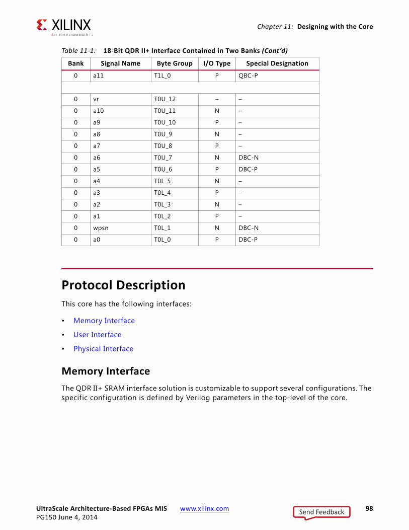
UltraScale Architecture-Based FPGAs MIS www.xilinx.com 98PG150 June 4, 2014
Chapter 11: Designing with the Core
Protocol DescriptionThis core has the following interfaces:
• Memory Interface
• User Interface
• Physical Interface
Memory InterfaceThe QDR II+ SRAM interface solution is customizable to support several configurations. The specific configuration is defined by Verilog parameters in the top-level of the core.
0 a11 T1L_0 P QBC-P
0 vr T0U_12 – –
0 a10 T0U_11 N –
0 a9 T0U_10 P –
0 a8 T0U_9 N –
0 a7 T0U_8 P –
0 a6 T0U_7 N DBC-N
0 a5 T0U_6 P DBC-P
0 a4 T0L_5 N –
0 a3 T0L_4 P –
0 a2 T0L_3 N –
0 a1 T0L_2 P –
0 wpsn T0L_1 N DBC-N
0 a0 T0L_0 P DBC-P
Table 11-1: 18-Bit QDR II+ Interface Contained in Two Banks (Cont’d)
Bank Signal Name Byte Group I/O Type Special Designation
Send Feedback
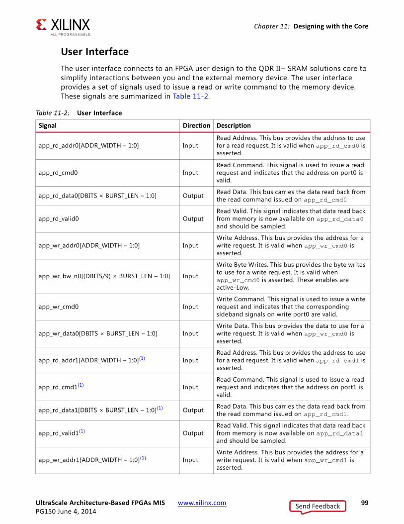
UltraScale Architecture-Based FPGAs MIS www.xilinx.com 99PG150 June 4, 2014
Chapter 11: Designing with the Core
User InterfaceThe user interface connects to an FPGA user design to the QDR II+ SRAM solutions core to simplify interactions between you and the external memory device. The user interface provides a set of signals used to issue a read or write command to the memory device. These signals are summarized in Table 11-2.
Table 11-2: User Interface
Signal Direction Description
app_rd_addr0[ADDR_WIDTH – 1:0] InputRead Address. This bus provides the address to use for a read request. It is valid when app_rd_cmd0 is asserted.
app_rd_cmd0 InputRead Command. This signal is used to issue a read request and indicates that the address on port0 is valid.
app_rd_data0[DBITS × BURST_LEN – 1:0] Output Read Data. This bus carries the data read back from the read command issued on app_rd_cmd0
app_rd_valid0 Output Read Valid. This signal indicates that data read back from memory is now available on app_rd_data0 and should be sampled.
app_wr_addr0[ADDR_WIDTH – 1:0] InputWrite Address. This bus provides the address for a write request. It is valid when app_wr_cmd0 is asserted.
app_wr_bw_n0[(DBITS/9) × BURST_LEN – 1:0] Input
Write Byte Writes. This bus provides the byte writes to use for a write request. It is valid when app_wr_cmd0 is asserted. These enables are active-Low.
app_wr_cmd0 InputWrite Command. This signal is used to issue a write request and indicates that the corresponding sideband signals on write port0 are valid.
app_wr_data0[DBITS × BURST_LEN – 1:0] InputWrite Data. This bus provides the data to use for a write request. It is valid when app_wr_cmd0 is asserted.
app_rd_addr1[ADDR_WIDTH – 1:0](1) InputRead Address. This bus provides the address to use for a read request. It is valid when app_rd_cmd1 is asserted.
app_rd_cmd1(1) InputRead Command. This signal is used to issue a read request and indicates that the address on port1 is valid.
app_rd_data1[DBITS × BURST_LEN – 1:0](1) Output Read Data. This bus carries the data read back from the read command issued on app_rd_cmd1.
app_rd_valid1(1) OutputRead Valid. This signal indicates that data read back from memory is now available on app_rd_data1 and should be sampled.
app_wr_addr1[ADDR_WIDTH – 1:0](1) InputWrite Address. This bus provides the address for a write request. It is valid when app_wr_cmd1 is asserted.
Send Feedback
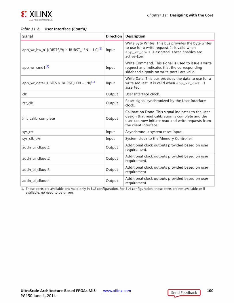
UltraScale Architecture-Based FPGAs MIS www.xilinx.com 100PG150 June 4, 2014
Chapter 11: Designing with the Core
app_wr_bw_n1[(DBITS/9) × BURST_LEN – 1:0](1) Input
Write Byte Writes. This bus provides the byte writes to use for a write request. It is valid when app_wr_cmd1 is asserted. These enables are active-Low.
app_wr_cmd1(1) InputWrite Command. This signal is used to issue a write request and indicates that the corresponding sideband signals on write port1 are valid.
app_wr_data1[DBITS × BURST_LEN – 1:0](1) InputWrite Data. This bus provides the data to use for a write request. It is valid when app_wr_cmd1 is asserted.
clk Output User Interface clock.
rst_clk Output Reset signal synchronized by the User Interface clock.
Init_calib_complete Output
Calibration Done. This signal indicates to the user design that read calibration is complete and the user can now initiate read and write requests from the client interface.
sys_rst Input Asynchronous system reset input.
sys_clk_p/n Input System clock to the Memory Controller.
addn_ui_clkout1 Output Additional clock outputs provided based on user requirement.
addn_ui_clkout2 Output Additional clock outputs provided based on user requirement.
addn_ui_clkout3 Output Additional clock outputs provided based on user requirement.
addn_ui_clkout4 Output Additional clock outputs provided based on user requirement.
1. These ports are available and valid only in BL2 configuration. For BL4 configuration, these ports are not available or if available, no need to be driven.
Table 11-2: User Interface (Cont’d)
Signal Direction Description
Send Feedback
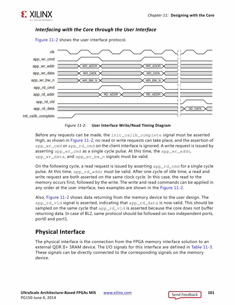
UltraScale Architecture-Based FPGAs MIS www.xilinx.com 101PG150 June 4, 2014
Chapter 11: Designing with the Core
Interfacing with the Core through the User Interface
Figure 11-2 shows the user interface protocol.
Before any requests can be made, the init_calib_complete signal must be asserted High, as shown in Figure 11-2, no read or write requests can take place, and the assertion of app_wr_cmd or app_rd_cmd on the client interface is ignored. A write request is issued by asserting app_wr_cmd as a single cycle pulse. At this time, the app_wr_addr, app_wr_data, and app_wr_bw_n signals must be valid.
On the following cycle, a read request is issued by asserting app_rd_cmd for a single cycle pulse. At this time, app_rd_addr must be valid. After one cycle of idle time, a read and write request are both asserted on the same clock cycle. In this case, the read to the memory occurs f irst, followed by the write. The write and read commands can be applied in any order at the user interface, two examples are shown in the Figure 11-2.
Also, Figure 11-2 shows data returning from the memory device to the user design. The app_rd_vld signal is asserted, indicating that app_rd_data is now valid. This should be sampled on the same cycle that app_rd_vld is asserted because the core does not buffer returning data. In case of BL2, same protocol should be followed on two independent ports, port0 and port1.
Physical InterfaceThe physical interface is the connection from the FPGA memory interface solution to an external QDR II+ SRAM device. The I/O signals for this interface are defined in Table 11-3. These signals can be directly connected to the corresponding signals on the memory device.
X-Ref Target - Figure 11-2
Figure 11-2: User Interface Write/Read Timing Diagram
Send Feedback
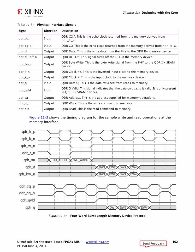
UltraScale Architecture-Based FPGAs MIS www.xilinx.com 102PG150 June 4, 2014
Chapter 11: Designing with the Core
Figure 11-3 shows the timing diagram for the sample write and read operations at the memory interface.
Table 11-3: Physical Interface Signals
Signal Direction Description
qdr_cq_n Input QDR CQ#. This is the echo clock returned from the memory derived from qdr_k_n.
qdr_cq_p Input QDR CQ. This is the echo clock returned from the memory derived from qdr_k_p.
qdr_d Output QDR Data. This is the write data from the PHY to the QDR II+ memory device.
qdr_dll_off_n Output QDR DLL Off. This signal turns off the DLL in the memory device.
qdr_bw_n Output QDR Byte Write. This is the byte write signal from the PHY to the QDR II+ SRAM device.
qdr_k_n Output QDR Clock K#. This is the inverted input clock to the memory device.
qdr_k_p Output QDR Clock K. This is the input clock to the memory device.
qdr_q Input QDR Data Q. This is the data returned from reads to memory.
qdr_qvld Input QDR Q Valid. This signal indicates that the data on qdr_q is valid. It is only present in QDR II+ SRAM devices.
qdr_sa Output QDR Address. This is the address supplied for memory operations.
qdr_w_n Output QDR Write. This is the write command to memory.
qdr_r_n Output QDR Read. This is the read command to memory.
X-Ref Target - Figure 11-3
Figure 11-3: Four-Word Burst Length Memory Device Protocol
Send Feedback
UltraScale Architecture-Based FPGAs MIS www.xilinx.com 103PG150 June 4, 2014
Chapter 12
Design Flow StepsThis chapter describes customizing and generating the core, constraining the core, and the simulation, synthesis and implementation steps that are specific to this IP core. More detailed information about the standard Vivado® design flows in the Vivado IP integrator can be found in the following Vivado Design Suite user guides:
• Vivado Design Suite User Guide: Designing IP Subsystems using IP Integrator (UG994) [Ref 5]
• Vivado Design Suite User Guide: Designing with IP (UG896) [Ref 6]
• Vivado Design Suite User Guide: Getting Started (UG910) [Ref 7]
• Vivado Design Suite User Guide: Logic Simulation (UG900) [Ref 8]
Customizing and Generating the CoreThis section includes information about using Xilinx® tools to customize and generate the core in the Vivado Design Suite.
If you are customizing and generating the core in the IP integrator, see the Vivado Design Suite User Guide: Designing IP Subsystems using IP Integrator (UG994) [Ref 5] for detailed information. IP integrator might auto-compute certain configuration values when validating or generating the design. To check whether the values change, see the description of the parameter in this chapter. To view the parameter value, run the validate_bd_design command in the Tcl Console.
You can customize the IP for use in your design by specifying values for the various parameters associated with the IP core using the following steps:
1. Select the IP from the IP catalog.
2. Double-click the selected IP or select the Customize IP command from the toolbar or right-click menu.
For details, see the Vivado Design Suite User Guide: Designing with IP (UG896) [Ref 6] and the Vivado Design Suite User Guide: Getting Started (UG910) [Ref 7].
Send Feedback
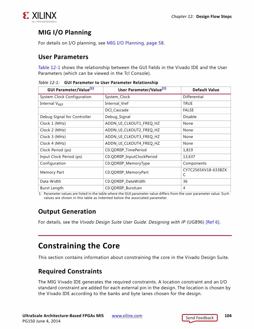
UltraScale Architecture-Based FPGAs MIS www.xilinx.com 104PG150 June 4, 2014
Chapter 12: Design Flow Steps
MIG I/O PlanningFor details on I/O planning, see MIG I/O Planning, page 58.
User ParametersTable 12-1 shows the relationship between the GUI f ields in the Vivado IDE and the User Parameters (which can be viewed in the Tcl Console).
Output GenerationFor details, see the Vivado Design Suite User Guide: Designing with IP (UG896) [Ref 6].
Constraining the CoreThis section contains information about constraining the core in the Vivado Design Suite.
Required ConstraintsThe MIG Vivado IDE generates the required constraints. A location constraint and an I/O standard constraint are added for each external pin in the design. The location is chosen by the Vivado IDE according to the banks and byte lanes chosen for the design.
Table 12-1: GUI Parameter to User Parameter RelationshipGUI Parameter/Value(1) User Parameter/Value(1) Default Value
System Clock Configuration System_Clock Differential
Internal VREF Internal_Vref TRUE
DCI_Cascade FALSE
Debug Signal for Controller Debug_Signal Disable
Clock 1 (MHz) ADDN_UI_CLKOUT1_FREQ_HZ None
Clock 2 (MHz) ADDN_UI_CLKOUT2_FREQ_HZ None
Clock 3 (MHz) ADDN_UI_CLKOUT3_FREQ_HZ None
Clock 4 (MHz) ADDN_UI_CLKOUT4_FREQ_HZ None
Clock Period (ps) C0.QDRIIP_TimePeriod 1,819
Input Clock Period (ps) C0.QDRIIP_InputClockPeriod 13,637
Configuration C0.QDRIIP_MemoryType Components
Memory Part C0.QDRIIP_MemoryPart CY7C2565XV18-633BZXC
Data Width C0.QDRIIP_DataWidth 36
Burst Length C0.QDRIIP_BurstLen 41. Parameter values are listed in the table where the GUI parameter value differs from the user parameter value. Such
values are shown in this table as indented below the associated parameter.
Send Feedback
UltraScale Architecture-Based FPGAs MIS www.xilinx.com 105PG150 June 4, 2014
Chapter 12: Design Flow Steps
The I/O standard is chosen by the memory type selection and options in the Vivado IDE and by the pin type. A sample for qdriip_d[0] is shown here.
set_property LOC AP25 [get_ports {c0_qdriip_d[0]}]set_property IOSTANDARD HSTL_I [get_ports {c0_qdriip_d[0]}]
The system clock must have the period set properly:
create_clock -name c0_sys_clk –period 1.818 [get_ports c0_sys_clk_p]
Device, Package, and Speed Grade SelectionsThis section is not applicable for this IP core.
Clock FrequenciesThis section is not applicable for this IP core.
Clock ManagementFor more information on clocking, see Clocking, page 91.
Clock PlacementThis section is not applicable for this IP core.
BankingThis section is not applicable for this IP core.
Transceiver PlacementThis section is not applicable for this IP core.
I/O Standard and PlacementThe MIG tool generates the appropriate I/O standards and placement based on the selections made in the Vivado IDE for the interface type and options.
IMPORTANT: The set_input_delay and set_output_delay constraints are not needed on the external memory interface pins in this design due to the calibration process that automatically runs at start-up. Warnings seen during implementation for the pins can be ignored.
Send Feedback
UltraScale Architecture-Based FPGAs MIS www.xilinx.com 106PG150 June 4, 2014
Chapter 12: Design Flow Steps
SimulationThis section contains information about simulating IP in the Vivado Design Suite. For comprehensive information about Vivado simulation components, as well as information about using supported third-party tools, see the Vivado Design Suite User Guide: Logic Simulation (UG900) [Ref 8].
Synthesis and ImplementationThis section contains information about synthesis and implementation in the Vivado Design Suite. For details about synthesis and implementation, see the Vivado Design Suite User Guide: Designing with IP (UG896) [Ref 6].
Send Feedback
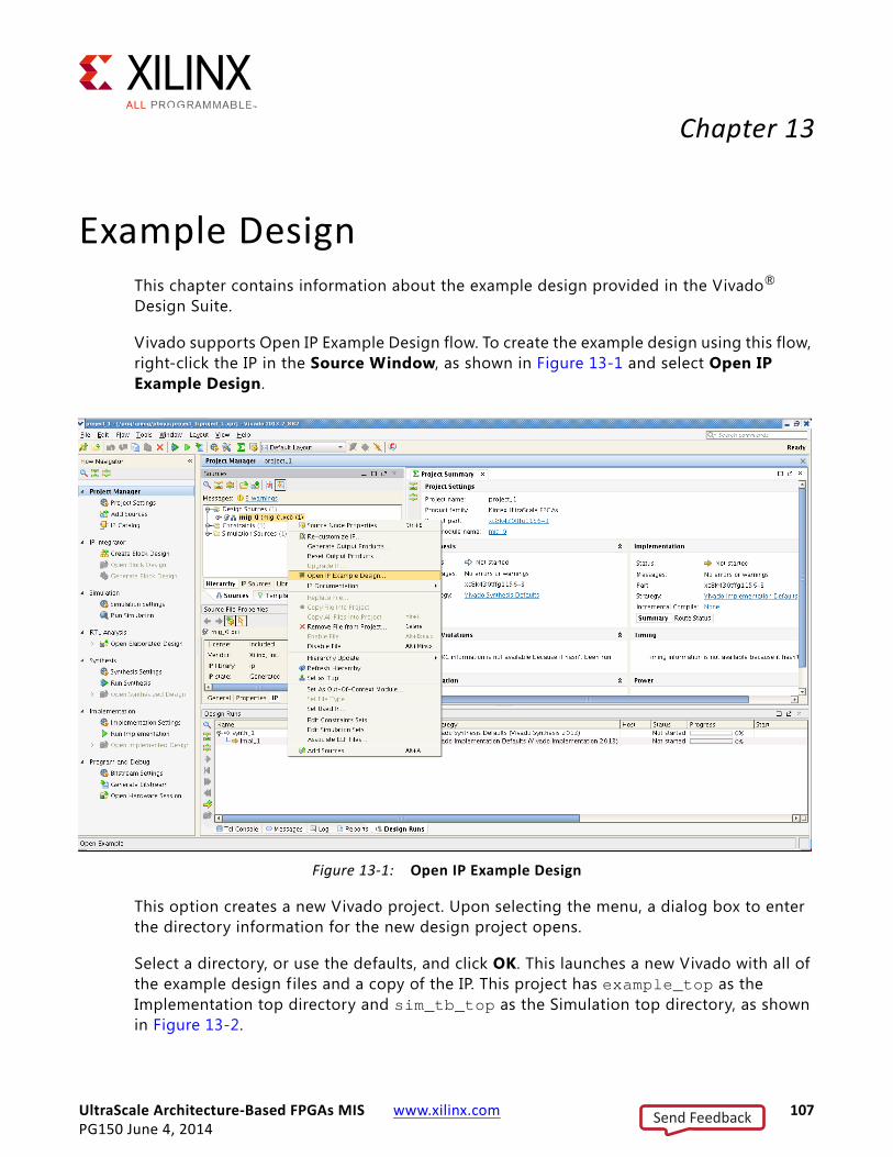
UltraScale Architecture-Based FPGAs MIS www.xilinx.com 107PG150 June 4, 2014
Chapter 13
Example DesignThis chapter contains information about the example design provided in the Vivado® Design Suite.
Vivado supports Open IP Example Design flow. To create the example design using this flow, right-click the IP in the Source Window, as shown in Figure 13-1 and select Open IP Example Design.
This option creates a new Vivado project. Upon selecting the menu, a dialog box to enter the directory information for the new design project opens.
Select a directory, or use the defaults, and click OK. This launches a new Vivado with all of the example design f iles and a copy of the IP. This project has example_top as the Implementation top directory and sim_tb_top as the Simulation top directory, as shown in Figure 13-2.
X-Ref Target - Figure 13-1
Figure 13-1: Open IP Example Design
Send Feedback
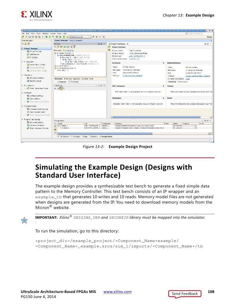
UltraScale Architecture-Based FPGAs MIS www.xilinx.com 108PG150 June 4, 2014
Chapter 13: Example Design
Simulating the Example Design (Designs with Standard User Interface)The example design provides a synthesizable test bench to generate a f ixed simple data pattern to the Memory Controller. This test bench consists of an IP wrapper and an example_tb that generates 10 writes and 10 reads. Memory model f iles are not generated when designs are generated from the IP. You need to download memory models from the Micron® website.
IMPORTANT: Xilinx® UNISIMS_VER and SECUREIP library must be mapped into the simulator.
To run the simulation, go to this directory:
<project_dir>/example_project/<Component_Name>example/<Component_Name>_example.srcs/sim_1/imports/<Component_Name>/tb
X-Ref Target - Figure 13-2
Figure 13-2: Example Design Project
Send Feedback
UltraScale Architecture-Based FPGAs MIS www.xilinx.com 109PG150 June 4, 2014
Chapter 13: Example Design
If the MIG design is generated with the Component Name entered in the Vivado IDE as mig_0, the simulation directory path is the following:
<project_dir>/example_project/mig_0_example/mig_0_example.srcs/sim_1/imports/mig_0/tb
MIG does not deliver the QDRII+ memory models. The memory models required for simulation must be obtained from the memory vendor directly. The Questa® SIM, IES, and VCS simulation tools are used for verif ication of MIG IP at each software release. Script f iles to run simulations with Questa SIM, IES, and VCS are generated in MIG generated output. MIG designs are not verif ied with Vivado Simulator. Other simulation tools can be used for MIG IP simulation but are not specifically verif ied by Xilinx.
Synplify Black Box TestingUsing the Synopsys® Synplify Pro® black box testing for example_design, follow these steps to run black box synthesis with synplify_pro and implementation with Vivado.
1. Generate the UltraScale™ architecture MIG IP core with OOC flow to generate the .dcp f ile for implementation. The Target Language for the project can be selected as verilog or VHDL.
2. Create the example design for the MIG IP core using the information provided in the example design section and close the Vivado project.
3. Invoke the synplify_pro software which supports UltraScale FPGA and select the same UltraScale FPGA part selected at the time of generating the IP core.
4. Add the following files into synplify_pro project based on the Target Language selected at the time of invoking Vivado:
a. For Verilog:
<project_dir>/example_project/<Component_Name>example/<Component_Name>_example.srcs/sources_1/ip/<Component_Name>/*stub.v<project_dir>/example_project/<Component_Name>example/<Component_Name>_example.srcs/sources_1/imports/<Component_Name>/rtl/ip_top/example_top.sv<project_dir>/example_project/<Component_Name>example/<Component_Name>_example.srcs/sources_1/imports/<Component_Name>/tb/example_tb.sv
b. For VHDL:
<project_dir>/example_project/<Component_Name>example/<Component_Name>_example.srcs/sources_1/ip/<Component_Name>/*stub.vhdl <project_dir>/example_project/<Component_Name>example/<Component_Name>_example.srcs/sources_1/imports/<Component_Name>/rtl/ip_top/example_top.sv<project_dir>/example_project/<Component_Name>example/<Component_Name>_example.srcs/sources_1/imports/<Component_Name>/tb/example_tb.sv
Send Feedback

UltraScale Architecture-Based FPGAs MIS www.xilinx.com 110PG150 June 4, 2014
Chapter 13: Example Design
5. Run synplify_pro synthesis to generate the .edf f ile. Then, close the synplify_pro project.
6. Open new Vivado project with Project Type as Post-synthesis Project and select the Target Language same as selected at the time of generating the IP core.
7. Add the synplify_pro generated .edf f ile to the Vivado project as Design Source.
8. Add the .dcp f ile generated in steps 1 and 2 to the Vivado project as Design Source. For example:
<project_dir>/example_project/<Component_Name>example/<Component_Name>_example.srcs/sources_1/ip/<Component_Name>/<Component_Name>.dcp
9. Add the .xdc f ile generated in step 2 to the Vivado project as constraint. For example:
<project_dir>/example_project/<Component_Name>example/<Component_Name>_example.srcs/constrs_1/imports/par/example_design.xdc
10. Run implementation flow with the Vivado tool. For details about implementation, see the Vivado Design Suite User Guide: Designing with IP (UG896) [Ref 6].
Note: Similar steps can be followed for the user design using appropriate .dcp and .xdc f iles.
Send Feedback

UltraScale Architecture-Based FPGAs MIS www.xilinx.com 111PG150 June 4, 2014
Chapter 14
Test BenchThis chapter contains information about the test bench provided in the Vivado® Design Suite.
The Memory Controller is generated along with a simple test bench to verify the basic read and write operations. The stimulus contains 10 consecutive writes followed by 10 consecutive reads for data integrity check.
Send Feedback
UltraScale Architecture-Based FPGAs MIS www.xilinx.com 112PG150 June 4, 2014
SECTION IV: RLDRAM 3
Overview
Product Specification
Core Architecture
Designing with the Core
Design Flow Steps
Example Design
Test Bench
Send Feedback
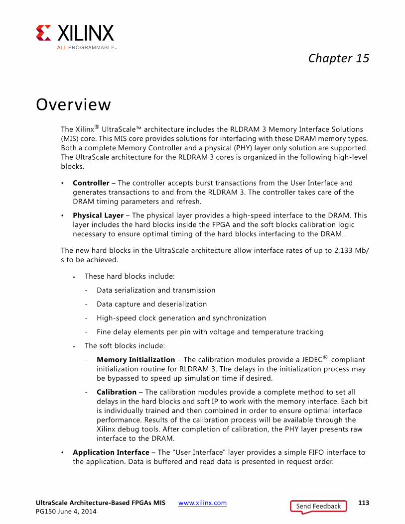
UltraScale Architecture-Based FPGAs MIS www.xilinx.com 113PG150 June 4, 2014
Chapter 15
OverviewThe Xilinx® UltraScale™ architecture includes the RLDRAM 3 Memory Interface Solutions (MIS) core. This MIS core provides solutions for interfacing with these DRAM memory types. Both a complete Memory Controller and a physical (PHY) layer only solution are supported. The UltraScale architecture for the RLDRAM 3 cores is organized in the following high-level blocks.
• Controller – The controller accepts burst transactions from the User Interface and generates transactions to and from the RLDRAM 3. The controller takes care of the DRAM timing parameters and refresh.
• Physical Layer – The physical layer provides a high-speed interface to the DRAM. This layer includes the hard blocks inside the FPGA and the soft blocks calibration logic necessary to ensure optimal timing of the hard blocks interfacing to the DRAM.
The new hard blocks in the UltraScale architecture allow interface rates of up to 2,133 Mb/s to be achieved.
° These hard blocks include:
- Data serialization and transmission
- Data capture and deserialization
- High-speed clock generation and synchronization
- Fine delay elements per pin with voltage and temperature tracking
° The soft blocks include:
- Memory Initialization – The calibration modules provide a JEDEC®-compliant initialization routine for RLDRAM 3. The delays in the initialization process may be bypassed to speed up simulation time if desired.
- Calibration – The calibration modules provide a complete method to set all delays in the hard blocks and soft IP to work with the memory interface. Each bit is individually trained and then combined in order to ensure optimal interface performance. Results of the calibration process will be available through the Xilinx debug tools. After completion of calibration, the PHY layer presents raw interface to the DRAM.
• Application Interface – The "User Interface" layer provides a simple FIFO interface to the application. Data is buffered and read data is presented in request order.
Send Feedback
UltraScale Architecture-Based FPGAs MIS www.xilinx.com 114PG150 June 4, 2014
Chapter 15: Overview
Feature Summary• Component support for interface widths of 18 and 36 bits
• x18 and x36 memory device support
• 4-word and 8-word burst support
• Support for 5 to 16 cycles of Read Latency
• ODT support
• JEDEC-compliant RLDRAM 3 initialization support
• Source code delivery in Verilog
• 4:1 memory to FPGA logic interface clock ratio
X-Ref Target - Figure 15-1
Figure 15-1: UltraScale Architecture-Based FPGAs Memory Interface Solution
Send Feedback
UltraScale Architecture-Based FPGAs MIS www.xilinx.com 115PG150 June 4, 2014
Chapter 15: Overview
Licensing and Ordering InformationThis Xilinx LogiCORE IP module is provided at no additional cost with the Xilinx Vivado Design Suite under the terms of the Xilinx End User License. Information about this and other Xilinx LogiCORE IP modules is available at the Xilinx Intellectual Property page. For information about pricing and availability of other Xilinx LogiCORE IP modules and tools, contact your local Xilinx sales representative.
License CheckersIf the IP requires a license key, the key must be verif ied. The Vivado® design tools have several license checkpoints for gating licensed IP through the flow. If the license check succeeds, the IP can continue generation. Otherwise, generation halts with error. License checkpoints are enforced by the following tools:
• Vivado design tools: Vivado Synthesis
• Vivado Implementation
• write_bitstream (Tcl command)
IMPORTANT: IP license level is ignored at checkpoints. The test confirms a valid license exists. It does not check IP license level.
Send Feedback
UltraScale Architecture-Based FPGAs MIS www.xilinx.com 116PG150 June 4, 2014
Chapter 16
Product Specification
StandardsFor more information on UltraScale™ architecture documents, see References, page 155.
Performance
Maximum FrequenciesFor more information on the maximum frequencies, see Kintex UltraScale Architecture Data Sheet, DC and AC Switching Characteristics (DS892) [Ref 2].
Resource Utilization
Kintex UltraScale DevicesTable 16-1 provides approximate resource counts on Kintex® UltraScale™ devices.
Resources required for the UltraScale architecture-based FPGAs MIS core have been estimated for the Kintex UltraScale devices. These values were generated using Vivado® IP catalog. They are derived from post-synthesis reports, and might change during implementation.
Table 16-1: Device Utilization – Kintex UltraScale FPGAs
Parameter Values Device Resources
Interface Width FFs LUTs Memory LUTs RAMB36E2/RAMB18E2 BUFGs PLLE3_ADV MMCME3_ADV
36 4,586 4,570 463 24 4 2 1
Send Feedback
UltraScale Architecture-Based FPGAs MIS www.xilinx.com 117PG150 June 4, 2014
Chapter 16: Product Specification
Port DescriptionsThere are three port categories at the top-level of the memory interface core called the “user design.”
• The first category is the memory interface signals that directly interfaces with the RLDRAM. These are defined by the RLDRAM 3 specif ication.
• The second category is the application interface signals which is the “user interface.” These are described in the Protocol Description, page 134.
• The third category includes other signals necessary for proper operation of the core. These include the clocks, reset, and status signals from the core. The clocking and reset signals are described in their respective sections.
The active-High init_calib_complete signal indicates that the initialization and calibration are complete and that the interface is now ready to accept commands for the interface.
Send Feedback
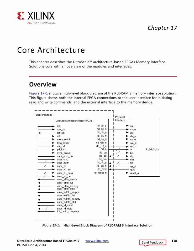
UltraScale Architecture-Based FPGAs MIS www.xilinx.com 118PG150 June 4, 2014
Chapter 17
Core ArchitectureThis chapter describes the UltraScale™ architecture-based FPGAs Memory Interface Solutions core with an overview of the modules and interfaces.
OverviewFigure 17-1 shows a high-level block diagram of the RLDRAM 3 memory interface solution. This f igure shows both the internal FPGA connections to the user interface for initiating read and write commands, and the external interface to the memory device.
X-Ref Target - Figure 17-1
Figure 17-1: High-Level Block Diagram of RLDRAM 3 Interface Solution
Send Feedback
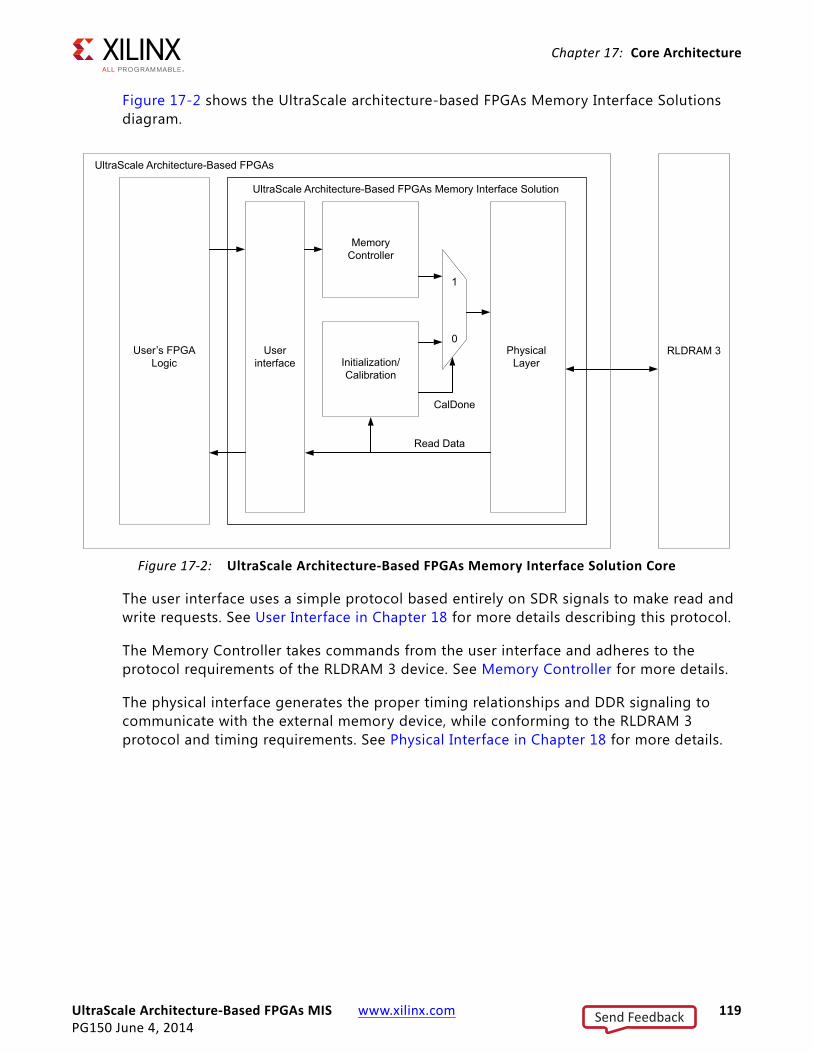
UltraScale Architecture-Based FPGAs MIS www.xilinx.com 119PG150 June 4, 2014
Chapter 17: Core Architecture
Figure 17-2 shows the UltraScale architecture-based FPGAs Memory Interface Solutions diagram.
The user interface uses a simple protocol based entirely on SDR signals to make read and write requests. See User Interface in Chapter 18 for more details describing this protocol.
The Memory Controller takes commands from the user interface and adheres to the protocol requirements of the RLDRAM 3 device. See Memory Controller for more details.
The physical interface generates the proper timing relationships and DDR signaling to communicate with the external memory device, while conforming to the RLDRAM 3 protocol and timing requirements. See Physical Interface in Chapter 18 for more details.
X-Ref Target - Figure 17-2
Figure 17-2: UltraScale Architecture-Based FPGAs Memory Interface Solution Core
Send Feedback
UltraScale Architecture-Based FPGAs MIS www.xilinx.com 120PG150 June 4, 2014
Chapter 17: Core Architecture
Memory ControllerThe Memory Controller (MC) enforces the RLDRAM 3 access requirements and interfaces with the PHY. The controller processes commands in order, so the order of commands presented to the controller is the order in which they are presented to the memory device.
The MC first receives commands from the user interface and determines if the command can be processed immediately or needs to wait. When all requirements are met, the command is placed on the PHY interface. For a write command, the controller generates a signal for the user interface to provide the write data to the PHY. This signal is generated based on the memory configuration to ensure the proper command-to-data relationship. Auto-refresh commands are inserted into the command flow by the controller to meet the memory device refresh requirements.
For CIO devices, the data bus is shared for read and write data. Switching from read commands to write commands and vice versa introduces gaps in the command stream due to switching the bus. For better throughput, changes in the command bus should be minimized when possible.
CMD_PER_CLK is a top-level parameter used to determine how many memory commands are provided to the controller per FPGA logic clock cycle. It depends on nCK_PER_CLK and the burst length. For example if nCK_PER_CLK = 4, the CMD_PER_CLK is set to 1 for burst length = 8 and CMD_PER_CLK is set to 2 for burst length = 4.
The controller remains in the CTL_IDLE state until calibration completes. When the calibration done signal is asserted and a command request is received, the state machine transitions to CTL_LOAD_CMD2 through the CTL_LOAD_CMD1 state (essentially a pipeline state).
For a single command request the controller state machine transitions from CTL_LOAD_CMD2 to CTL_PROC_LAST_CMD and back to CTL_IDLE.
For multiple commands to the same RLDRAM 3 bank and CMD_PER_CLK = 1, the state machine transitions from CTL_LOAD_CMD2 → CTL_PROC_CMD → CTL_PROC_CMD1 → CTL_PROC_LAST_CMD → CTL_IDLE.
For multiple commands to the same RLDRAM 3 bank and CMD_PER_CLK > 1, the state machine transitions from CTL_LOAD_CMD2 → CTL_PROC_CMD → CTL_PROC_CMD1 → CTL_PROC_LAST_CMD → CTL_PROC_LAST_CMD1 → CTL_IDLE.
For multiple commands to different RLDRAM 3 banks and CMD_PER_CLK = 1, the state machine transitions from CTL_LOAD_CMD2 → CTL_PROC_CMD → CTL_PROC_LAST_CMD → CTL_IDLE.
Send Feedback
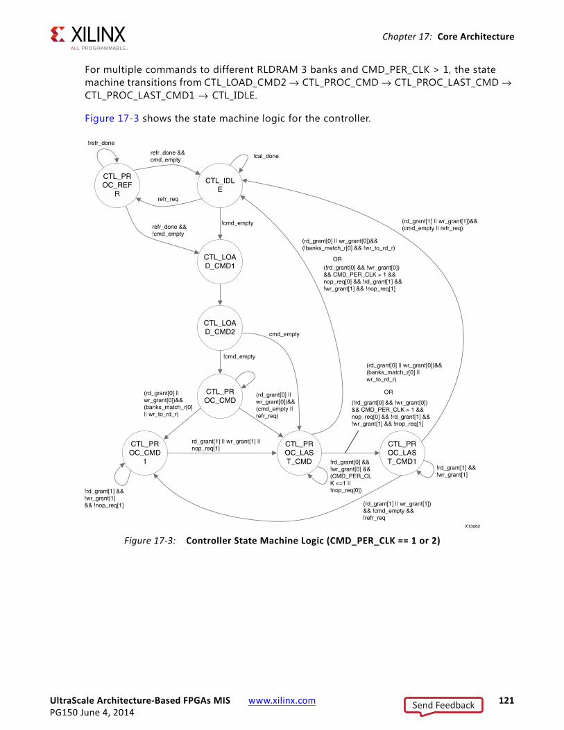
UltraScale Architecture-Based FPGAs MIS www.xilinx.com 121PG150 June 4, 2014
Chapter 17: Core Architecture
For multiple commands to different RLDRAM 3 banks and CMD_PER_CLK > 1, the state machine transitions from CTL_LOAD_CMD2 → CTL_PROC_CMD → CTL_PROC_LAST_CMD → CTL_PROC_LAST_CMD1 → CTL_IDLE.
Figure 17-3 shows the state machine logic for the controller.
X-Ref Target - Figure 17-3
Figure 17-3: Controller State Machine Logic (CMD_PER_CLK == 1 or 2)
Send Feedback
UltraScale Architecture-Based FPGAs MIS www.xilinx.com 122PG150 June 4, 2014
Chapter 17: Core Architecture
PHYPHY is considered the low-level physical interface to an external RLDRAM 3 device as well as all calibration logic for ensuring reliable operation of the physical interface itself. PHY generates the signal timing and sequencing required to interface to the memory device.
PHY contains the following features:
• Clock/address/control-generation logics
• Write and read datapaths
• Logic for initializing the SDRAM after power-up
In addition, PHY contains calibration logic to perform timing training of the read and write datapaths to account for system static and dynamic delays.
Overall PHY ArchitectureThe UltraScale architecture PHY is composed of dedicated blocks and soft calibration logic. The dedicated blocks are structured adjacent to one another with back-to-back interconnects to minimize the clock and datapath routing necessary to build high performance physical layers.
The Memory Controller and calibration logic communicate with this dedicated PHY in the slow frequency clock domain, which is either divided by 4 or divided by 2. This depends on the RLDRAM 3 memory clock. A more detailed block diagram of the PHY design is shown in Figure 17-4.
Send Feedback
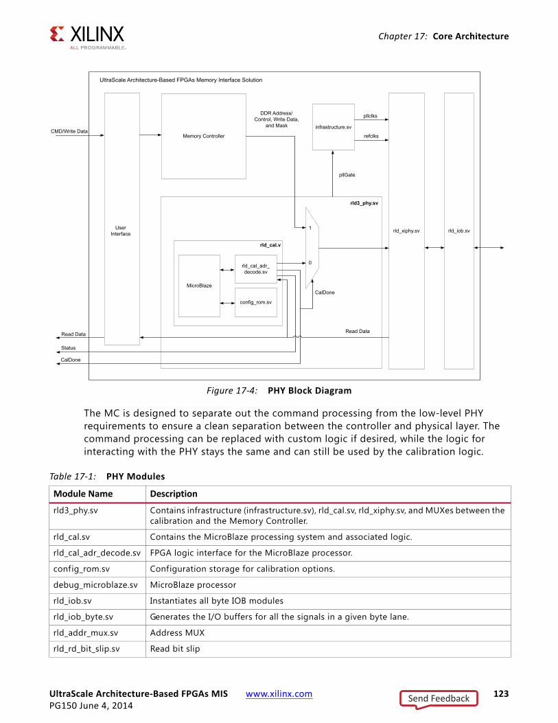
UltraScale Architecture-Based FPGAs MIS www.xilinx.com 123PG150 June 4, 2014
Chapter 17: Core Architecture
The MC is designed to separate out the command processing from the low-level PHY requirements to ensure a clean separation between the controller and physical layer. The command processing can be replaced with custom logic if desired, while the logic for interacting with the PHY stays the same and can still be used by the calibration logic.
X-Ref Target - Figure 17-4
Figure 17-4: PHY Block Diagram
Table 17-1: PHY Modules
Module Name Description
rld3_phy.sv Contains infrastructure (infrastructure.sv), rld_cal.sv, rld_xiphy.sv, and MUXes between the calibration and the Memory Controller.
rld_cal.sv Contains the MicroBlaze processing system and associated logic.
rld_cal_adr_decode.sv FPGA logic interface for the MicroBlaze processor.
config_rom.sv Configuration storage for calibration options.
debug_microblaze.sv MicroBlaze processor
rld_iob.sv Instantiates all byte IOB modules
rld_iob_byte.sv Generates the I/O buffers for all the signals in a given byte lane.
rld_addr_mux.sv Address MUX
rld_rd_bit_slip.sv Read bit slip
Send Feedback
UltraScale Architecture-Based FPGAs MIS www.xilinx.com 124PG150 June 4, 2014
Chapter 17: Core Architecture
The PHY architecture encompasses all of the logic contained in rld_xiphy.sv. The PHY contains wrappers around dedicated hard blocks to build up the memory interface from smaller components. A byte lane contains all of the clocks, resets, and datapaths for a given subset of I/O. Multiple byte lanes are grouped together, along with dedicated clocking resources, to make up a single bank memory interface. For more information on the hard silicon physical layer architecture, see the UltraScale™ Architecture-Based FPGAs SelectIO™ Resources User Guide (UG571) [Ref 3].
The memory initialization and calibration are implemented in C programming on a small soft core processor. The MicroBlaze™ Controller System (MCS) is configured with an I/O Module and block RAM. The rld_cal_adr_decode.sv module provides the interface for the processor to the rest of the system and implements helper logic. The config_rom.sv module stores settings that control the operation of initialization and calibration, providing run time options that can be adjusted without having to recompile the source code.
The address unit connects the MCS to the local register set and the PHY by performing address decode and control translation on the I/O module bus from spaces in the memory map and MUXing return data (rld_cal_adr_decode.sv). In addition, it provides address translation (also known as “mapping”) from a logical conceptualization of the DRAM interface to the appropriate pinout-dependent location of the delay control in the PHY address space.
Although the calibration architecture presents a simple and organized address map for manipulating the delay elements for individual data, control and command bits, there is flexibility in how those I/O pins are placed. For a given I/O placement, the path to the FPGA logic is locked to a given pin. To enable a single binary software f ile to work with any memory interface pinout, a translation block converts the simplif ied RIU addressing into the pinout-specific RIU address for the target design. The specif ic address translation is written by MIG after a pinout is selected. The code shows an example of the RTL structure that supports this.
Casez(io_address)// MicroBlaze I/O module address // … static address decoding skipped //========================================// //===========DQ ODELAYS===================// //========================================// //Byte0 28’h0004100: begin //dq2 riu_addr_cal = /* MIG Generated */ 6’hd; riu_nibble = /* MIG Generated */ ‘h0; end // … additional dynamic addressing follows
rld_wr_lat.sv Write latency
rld_xiphy.sv Top-level XIPHY module
Table 17-1: PHY Modules (Cont’d)
Module Name Description
Send Feedback
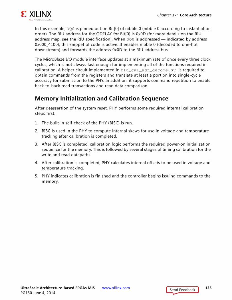
UltraScale Architecture-Based FPGAs MIS www.xilinx.com 125PG150 June 4, 2014
Chapter 17: Core Architecture
In this example, DQ0 is pinned out on Bit[0] of nibble 0 (nibble 0 according to instantiation order). The RIU address for the ODELAY for Bit[0] is 0x0D (for more details on the RIU address map, see the RIU specification). When DQ0 is addressed — indicated by address 0x000_4100), this snippet of code is active. It enables nibble 0 (decoded to one-hot downstream) and forwards the address 0x0D to the RIU address bus.
The MicroBlaze I/O module interface updates at a maximum rate of once every three clock cycles, which is not always fast enough for implementing all of the functions required in calibration. A helper circuit implemented in rld_cal_adr_decode.sv is required to obtain commands from the registers and translate at least a portion into single-cycle accuracy for submission to the PHY. In addition, it supports command repetition to enable back-to-back read transactions and read data comparison.
Memory Initialization and Calibration SequenceAfter deassertion of the system reset, PHY performs some required internal calibration steps first.
1. The built-in self-check of the PHY (BISC) is run.
2. BISC is used in the PHY to compute internal skews for use in voltage and temperature tracking after calibration is completed.
3. After BISC is completed, calibration logic performs the required power-on initialization sequence for the memory. This is followed by several stages of timing calibration for the write and read datapaths.
4. After calibration is completed, PHY calculates internal offsets to be used in voltage and temperature tracking.
5. PHY indicates calibration is f inished and the controller begins issuing commands to the memory.
Send Feedback
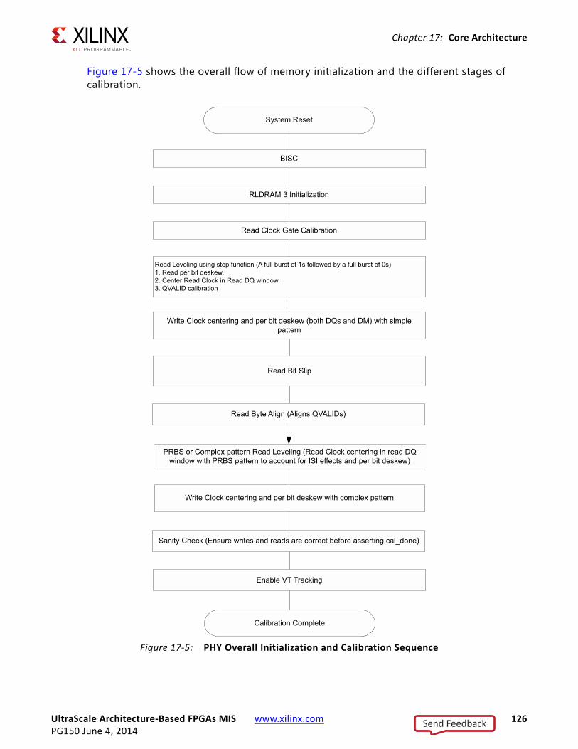
UltraScale Architecture-Based FPGAs MIS www.xilinx.com 126PG150 June 4, 2014
Chapter 17: Core Architecture
Figure 17-5 shows the overall flow of memory initialization and the different stages of calibration.
X-Ref Target - Figure 17-5
Figure 17-5: PHY Overall Initialization and Calibration Sequence
Send Feedback
UltraScale Architecture-Based FPGAs MIS www.xilinx.com 127PG150 June 4, 2014
Chapter 18
Designing with the CoreThis chapter includes guidelines and additional information to facilitate designing with the core.
ClockingThe memory interface requires one MMCM, one TXPLL per I/O bank used by the memory interface, two BUFGs, and one BUFGCE_DIV. These clocking components are used to create the proper clock frequencies and phase shifts necessary for the proper operation of the memory interface.
There are two TXPLLs per bank. If a bank is shared by two memory interfaces, both TXPLLs in that bank are used.
Note: MIG generates the appropriate clocking structure and no modifications to the RTL are supported.
The MIG tool generates the appropriate clocking structure for the desired interface. This structure must not be modif ied. The allowed clock configuration is as follows:
• Differential reference clock source connected to GCIO
• GCIO to MMCM (located in same bank as GCIO)
• MMCM to BUFG (located in same bank as MMCM)
• BUFG (at MMCM) to BUFG (located at center bank of memory interface) driving FPGA logic and all TXPLLs
• BUFG (at MMCM) to BUFGCE_DIV (located at center bank of memory interface) divide by two mode driving 1/2 rate FPGA logic
• Clocking pair of the interface must be in the same SLR of memory interface for the SSI technology devices
Send Feedback

UltraScale Architecture-Based FPGAs MIS www.xilinx.com 128PG150 June 4, 2014
Chapter 18: Designing with the Core
Requirements
GCIO
• Must use a differential I/O standard
• Must be in the same I/O column as the memory interface
MMCM
• MMCM is used to generate the FPGA logic system clock (1/4 of the memory clock)
• Must be located in the same bank as the GCIO
• Must use internal feedback
• Input clock frequency divided by input divider must be ≥ 70 MHz (CLKINx / D ≥ 70 MHz)
• Must use integer multiply and output divide values
BUFG and Clock Root at MMCM
• Must be placed in the same bank as the MMCM
BUFG/BUFGCE_DIV and Clock Roots
• BUFGCE_DIV is used to divide the system clock by two.
• BUFGCE_DIV and BUFG and clock roots must be located in center most bank of the memory interface.
° For two bank systems, either bank can be used. MIG is always referred to the top-most selected bank in the GUI as the center bank.
° For four bank systems, either of the center banks can be chosen. MIG refers to the second bank from the top-most selected bank as the center bank.
° BUFG and BUFGCE_DIV must be in the same bank.
TXPLL
• CLKOUTPHY from TXPLL drives XiPhy within its bank
• TXPLL must be set to use a CLKFBOUT phase shift of 90°
• TXPLL must be held in reset until the MMCM lock output goes High
• Must use internal feedback
Send Feedback
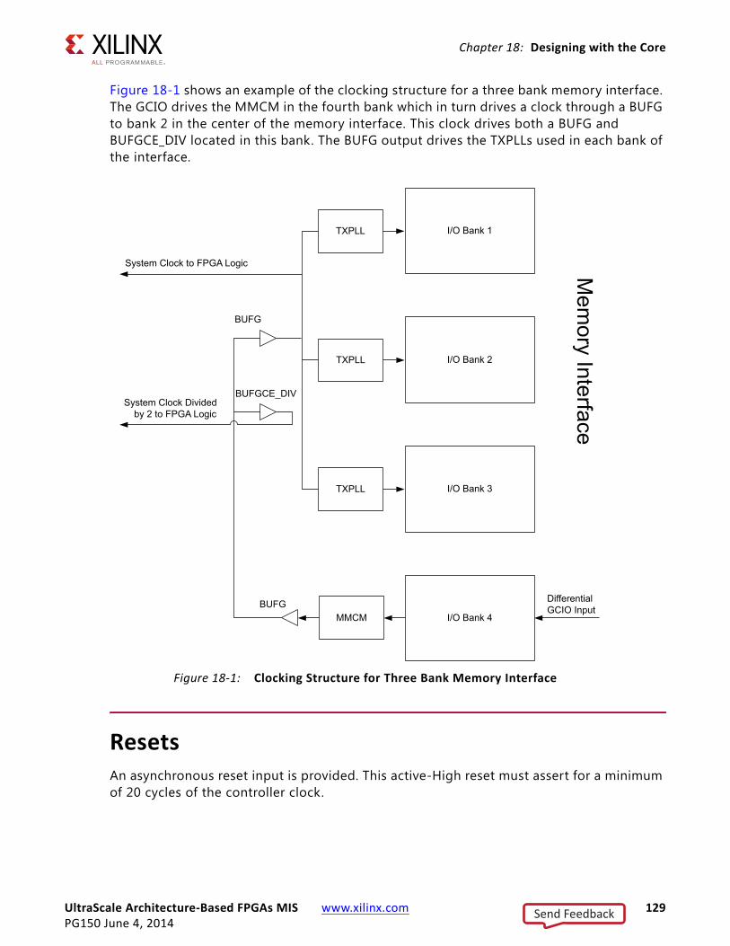
UltraScale Architecture-Based FPGAs MIS www.xilinx.com 129PG150 June 4, 2014
Chapter 18: Designing with the Core
Figure 18-1 shows an example of the clocking structure for a three bank memory interface. The GCIO drives the MMCM in the fourth bank which in turn drives a clock through a BUFG to bank 2 in the center of the memory interface. This clock drives both a BUFG and BUFGCE_DIV located in this bank. The BUFG output drives the TXPLLs used in each bank of the interface.
ResetsAn asynchronous reset input is provided. This active-High reset must assert for a minimum of 20 cycles of the controller clock.
X-Ref Target - Figure 18-1
Figure 18-1: Clocking Structure for Three Bank Memory Interface
Send Feedback
UltraScale Architecture-Based FPGAs MIS www.xilinx.com 130PG150 June 4, 2014
Chapter 18: Designing with the Core
PCB Guidelines for RLDRAM 3Strict adherence to all documented RLDRAM 3 PCB guidelines is required for successful operation. For more information on PCB guidelines, see the UltraScale Architecture PCB Design and Pin Planning User Guide (UG583) [Ref 4].
Pin and Bank Rules
RLDRAM 3 Pin RulesThe rules are for single rank memory interfaces.
• Address/control means cs_n, ref_n, we_n, ba, ck , reset_n, and a.
• All groups such as, Data, Address/Control, and System clock interfaces must be selected in a single column.
• Pins in a byte lane are numbered N0 to N12.
• Byte lanes in a bank are designed by T0, T1, T2, or T3. Nibbles within a byte lane are distinguished by a “U” or “L” designator added to the byte lane designator (T0, T1, T2, or T3). Thus they are T0L, T0U, T1L, T1U, T2L, T2U, T3L, and T3U.
Note: There are two PLLs per bank and a controller uses one PLL in every bank that is being used by the interface.
1. Read Clock (qk/qk_n), Write Clock (dk/dk_n), dq, qvld, and dm.
a. Read Clock pairs (qkx_p/n) must be placed on N0 and N1 pins in the lower nibble of a byte lane designated with "L." dq associated with a qk/qk_n pair must be in same byte lane on any of the other pins except pin N12. dq and dm bits must be placed on pins N2 to N11 in a byte lane.
b. One dm pin is associated with nine bits in x18 devices or with 18 bits in x36 devices. It must be placed in its associated dq byte lanes as listed:
- For x18 part, dm[0] must be allocated in dq[8:0] allocated byte group and dm[1] must be allocated in dq[17:9].
- For x36 part, dm[0] must be allocated in dq[8:0] or dq[26:18] allocated byte lane. Similarly dm[1] must be allocated in dq[17:9] or dq[35:27] allocated byte group.
c. dk/dk_n must be allocated to any P-N pair in the same byte lane as ck/ck_n in the address/control bank.
Note: Note that pin 12 is not part of a pin pair and must not be used for differential clocks.
Send Feedback

UltraScale Architecture-Based FPGAs MIS www.xilinx.com 131PG150 June 4, 2014
Chapter 18: Designing with the Core
d. qvld signal must be placed on pins N2 to N12 but f irst priority must be given for dq and dm allocation. qvld0 signal must be placed on pin N11 of byte lane (if available, dm is disabled), or pin N12 of byte lane of the qk0/qk0_n data byte lane and qvld1 signal must be placed on pin N11 of byte lane (if available), or pin N12 of byte lane of the qk2/qk2_n data byte lane
2. Byte lanes are configured as either data or address/control.
a. Pin N12 can be used for address/control in a data byte lane.
b. No data signals (qvalid, dq, dm) can be placed in an address/control byte lane.
3. Address/control can be on any of the 13 pins in the address/control byte lanes. Address/control must be contained within the same bank. Address/control must be in the centermost bank.
4. There is one vr pin per bank and DCI is required. DCI cascade is not permitted. All rules for the DCI in the UltraScale™ Architecture-Based FPGAs SelectIO™ Resources User Guide (UG571) [Ref 3] must be followed.
5. ck must be on the PN pair in the Address/Control byte lane.
6. reset_n can be on any pin as long as FPGA logic timing is met and I/O standard can be accommodated for the chosen bank (LVCMOS12).
7. Banks can be shared between two controllers.
a. Each byte lane is dedicated to a specific controller (except for reset_n).
b. Byte lanes from one controller cannot be placed inside the other. For example, with controllers A and B, “AABB” is allowed, while “ABAB” is not.
8. All I/O banks used by the memory interface must be in the same column.
9. All I/O banks used by the memory interface must be in the same SLR of the column for the SSI technology devices.
10. Maximum height of interface is three contiguous banks for 72-bit wide interface.
11. Bank skipping is not allowed.
12. The input clock for the master PLL in the interface must come from the a clock capable pair in the I/O column used for the memory interface.
13. There are dedicated VREF pins (not included in the rules above). If an external VREF is not used, the VREF pins should be pulled to ground by a 500Ω resistor. For more information, see the UltraScale™ Architecture-Based FPGAs SelectIO™ Resources User Guide (UG571) [Ref 3]. These pins must be connected appropriately for the standard in use.
14. The interface must be contained within the same I/O bank type (High Range or High Performance). Mixing bank types is not permitted with the exceptions of the reset_n in step 6 above and the input clock mentioned in step 11 above.
Send Feedback
UltraScale Architecture-Based FPGAs MIS www.xilinx.com 132PG150 June 4, 2014
Chapter 18: Designing with the Core
RLDRAM 3 Pinout Examples
IMPORTANT: Due to the calibration stage, there is no need for set_input_delay/set_output_delay on the MIG. You need to ignore the unconstrained inputs and outputs for MIG and the signals which are calibrated.
Table 18-1 shows an example of an 18-bit RLDRAM 3 interface contained within one bank. This example is for a component interface using one x18 RLDRAM3 component with Address Multiplexing.
Table 18-1: 18-Bit RLDRAM 3 Interface Contained in One Bank
Bank Signal Name Byte Group I/O Type Special Designation
1 qvld0 T3U_12 – –
1 dq8 T3U_11 N –
1 dq7 T3U_10 P –
1 dq6 T3U_9 N –
1 dq5 T3U_8 P –
1 dq4 T3U_7 N DBC-N
1 dq3 T3U_6 P DBC-P
1 dq2 T3L_5 N –
1 dq1 T3L_4 P –
1 dq0 T3L_3 N –
1 dm0 T3L_2 P –
1 qk0_n T3L_1 N DBC-N
1 qk0_p T3L_0 P DBC-P
1 reset_n T2U_12 – –
1 we# T2U_11 N –
1 a18 T2U_10 P –
1 a17 T2U_9 N –
1 a14 T2U_8 P –
1 a13 T2U_7 N QBC-N
1 a10 T2U_6 P QBC-P
1 a9 T2L_5 N –
1 a8 T2L_4 P –
1 a5 T2L_3 N –
1 a4 T2L_2 P –
1 a3 T2L_1 N QBC-N
Send Feedback
UltraScale Architecture-Based FPGAs MIS www.xilinx.com 133PG150 June 4, 2014
Chapter 18: Designing with the Core
1 a0 T2L_0 P QBC-P
1 – T1U_12 – –
1 ba3 T1U_11 N –
1 ba2 T1U_10 P –
1 ba1 T1U_9 N –
1 ba0 T1U_8 P –
1 dk1_n T1U_7 N QBC-N
1 dk1_p T1U_6 P QBC-P
1 dk0_n T1L_5 N –
1 dk0_p T1L_4 P –
1 ck_n T1L_3 N –
1 ck_p T1L_2 P –
1 ref_n T1L_1 N QBC-N
1 cs_n T1L_0 P QBC-P
1 vr T0U_12 – –
1 dq17 T0U_11 N –
1 dq16 T0U_10 P –
1 dq15 T0U_9 N –
1 dq14 T0U_8 P –
1 dq13 T0U_7 N DBC-N
1 dq12 T0U_6 P DBC-P
1 dq11 T0L_5 N –
1 dq10 T0L_4 P –
1 dq9 T0L_3 N –
1 dm1 T0L_2 P –
1 qk1_n T0L_1 N DBC-N
1 qk1_p T0L_0 P DBC-P
Table 18-1: 18-Bit RLDRAM 3 Interface Contained in One Bank (Cont’d)
Bank Signal Name Byte Group I/O Type Special Designation
Send Feedback
UltraScale Architecture-Based FPGAs MIS www.xilinx.com 134PG150 June 4, 2014
Chapter 18: Designing with the Core
Protocol DescriptionThis core has the following interfaces:
• Memory Interface
• User Interface
• Physical Interface
Memory InterfaceThe RLDRAM 3 memory interface solution is customizable to support several configurations. The specific configuration is defined by Verilog parameters in the top-level of the core.
User InterfaceThe user interface connects to an FPGA user design to the RLDRAM 3 memory solutions core to simplify interactions between you and the external memory device.
Command Request Signals
The user interface provides a set of signals used to issue a read or write command to the memory device. These signals are summarized in Table 18-2.
Send Feedback
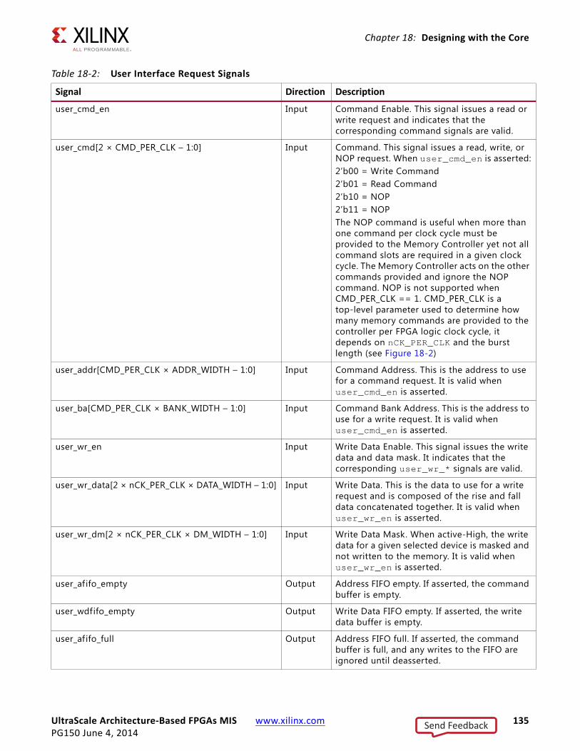
UltraScale Architecture-Based FPGAs MIS www.xilinx.com 135PG150 June 4, 2014
Chapter 18: Designing with the Core
Table 18-2: User Interface Request Signals
Signal Direction Description
user_cmd_en Input Command Enable. This signal issues a read or write request and indicates that the corresponding command signals are valid.
user_cmd[2 × CMD_PER_CLK – 1:0] Input Command. This signal issues a read, write, or NOP request. When user_cmd_en is asserted:2’b00 = Write Command2’b01 = Read Command2’b10 = NOP2’b11 = NOPThe NOP command is useful when more than one command per clock cycle must be provided to the Memory Controller yet not all command slots are required in a given clock cycle. The Memory Controller acts on the other commands provided and ignore the NOP command. NOP is not supported when CMD_PER_CLK == 1. CMD_PER_CLK is a top-level parameter used to determine how many memory commands are provided to the controller per FPGA logic clock cycle, it depends on nCK_PER_CLK and the burst length (see Figure 18-2)
user_addr[CMD_PER_CLK × ADDR_WIDTH – 1:0] Input Command Address. This is the address to use for a command request. It is valid when user_cmd_en is asserted.
user_ba[CMD_PER_CLK × BANK_WIDTH – 1:0] Input Command Bank Address. This is the address to use for a write request. It is valid when user_cmd_en is asserted.
user_wr_en Input Write Data Enable. This signal issues the write data and data mask. It indicates that the corresponding user_wr_* signals are valid.
user_wr_data[2 × nCK_PER_CLK × DATA_WIDTH – 1:0] Input Write Data. This is the data to use for a write request and is composed of the rise and fall data concatenated together. It is valid when user_wr_en is asserted.
user_wr_dm[2 × nCK_PER_CLK × DM_WIDTH – 1:0] Input Write Data Mask. When active-High, the write data for a given selected device is masked and not written to the memory. It is valid when user_wr_en is asserted.
user_afifo_empty Output Address FIFO empty. If asserted, the command buffer is empty.
user_wdfifo_empty Output Write Data FIFO empty. If asserted, the write data buffer is empty.
user_afifo_full Output Address FIFO full. If asserted, the command buffer is full, and any writes to the FIFO are ignored until deasserted.
Send Feedback
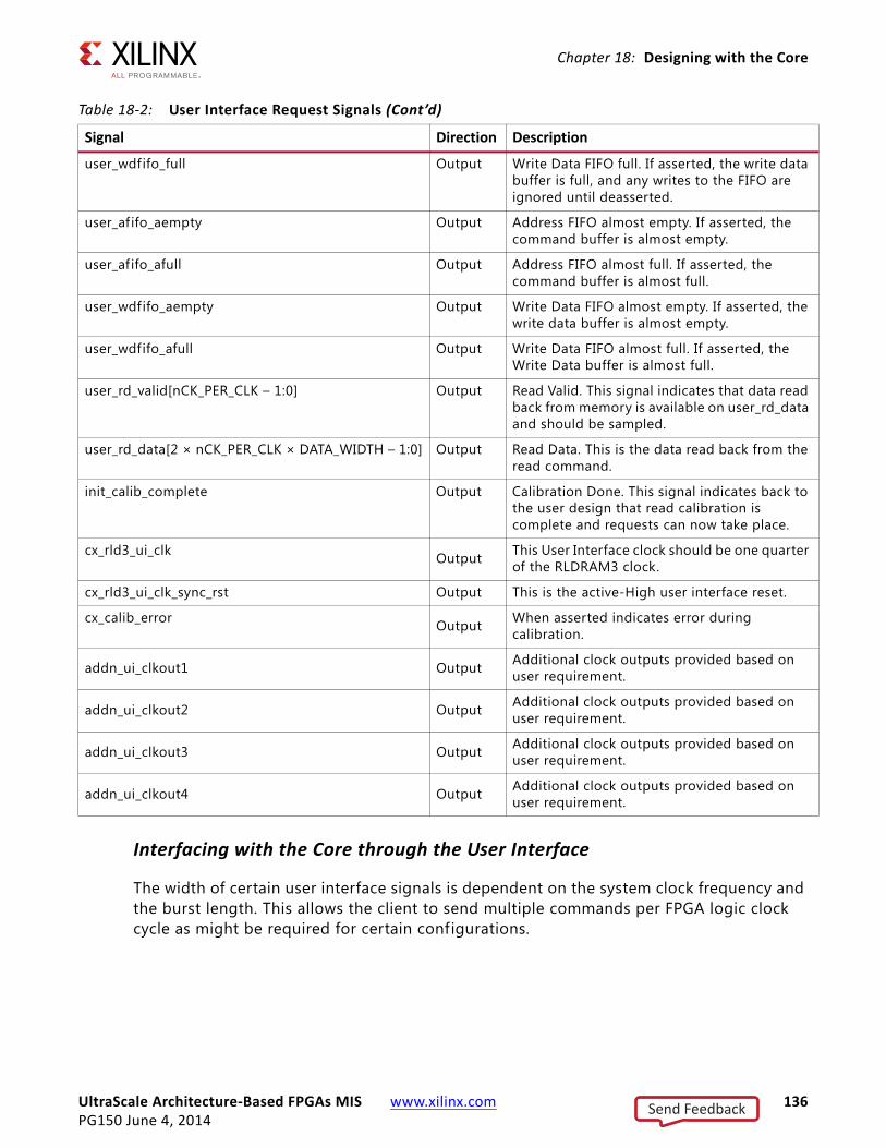
UltraScale Architecture-Based FPGAs MIS www.xilinx.com 136PG150 June 4, 2014
Chapter 18: Designing with the Core
Interfacing with the Core through the User Interface
The width of certain user interface signals is dependent on the system clock frequency and the burst length. This allows the client to send multiple commands per FPGA logic clock cycle as might be required for certain configurations.
user_wdfifo_full Output Write Data FIFO full. If asserted, the write data buffer is full, and any writes to the FIFO are ignored until deasserted.
user_afifo_aempty Output Address FIFO almost empty. If asserted, the command buffer is almost empty.
user_afifo_afull Output Address FIFO almost full. If asserted, the command buffer is almost full.
user_wdfifo_aempty Output Write Data FIFO almost empty. If asserted, the write data buffer is almost empty.
user_wdfifo_afull Output Write Data FIFO almost full. If asserted, the Write Data buffer is almost full.
user_rd_valid[nCK_PER_CLK – 1:0] Output Read Valid. This signal indicates that data read back from memory is available on user_rd_data and should be sampled.
user_rd_data[2 × nCK_PER_CLK × DATA_WIDTH – 1:0] Output Read Data. This is the data read back from the read command.
init_calib_complete Output Calibration Done. This signal indicates back to the user design that read calibration is complete and requests can now take place.
cx_rld3_ui_clk Output This User Interface clock should be one quarter of the RLDRAM3 clock.
cx_rld3_ui_clk_sync_rst Output This is the active-High user interface reset.
cx_calib_error Output When asserted indicates error during calibration.
addn_ui_clkout1 Output Additional clock outputs provided based on user requirement.
addn_ui_clkout2 Output Additional clock outputs provided based on user requirement.
addn_ui_clkout3 Output Additional clock outputs provided based on user requirement.
addn_ui_clkout4 Output Additional clock outputs provided based on user requirement.
Table 18-2: User Interface Request Signals (Cont’d)
Signal Direction Description
Send Feedback
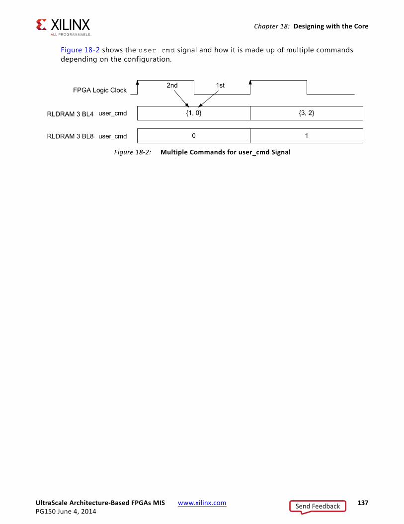
UltraScale Architecture-Based FPGAs MIS www.xilinx.com 137PG150 June 4, 2014
Chapter 18: Designing with the Core
Figure 18-2 shows the user_cmd signal and how it is made up of multiple commands depending on the configuration.
X-Ref Target - Figure 18-2
Figure 18-2: Multiple Commands for user_cmd Signal
Send Feedback
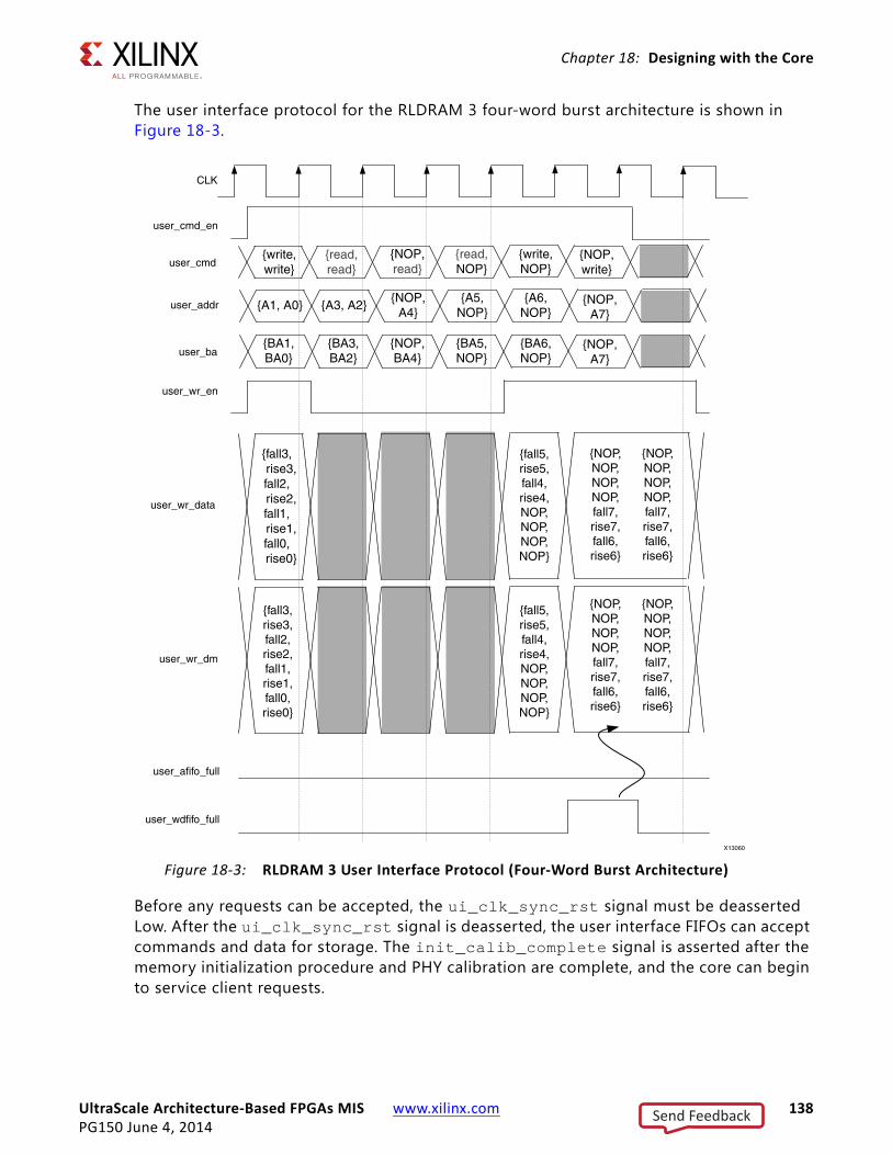
UltraScale Architecture-Based FPGAs MIS www.xilinx.com 138PG150 June 4, 2014
Chapter 18: Designing with the Core
The user interface protocol for the RLDRAM 3 four-word burst architecture is shown in Figure 18-3.
Before any requests can be accepted, the ui_clk_sync_rst signal must be deasserted Low. After the ui_clk_sync_rst signal is deasserted, the user interface FIFOs can accept commands and data for storage. The init_calib_complete signal is asserted after the memory initialization procedure and PHY calibration are complete, and the core can begin to service client requests.
X-Ref Target - Figure 18-3
Figure 18-3: RLDRAM 3 User Interface Protocol (Four-Word Burst Architecture)
Send Feedback
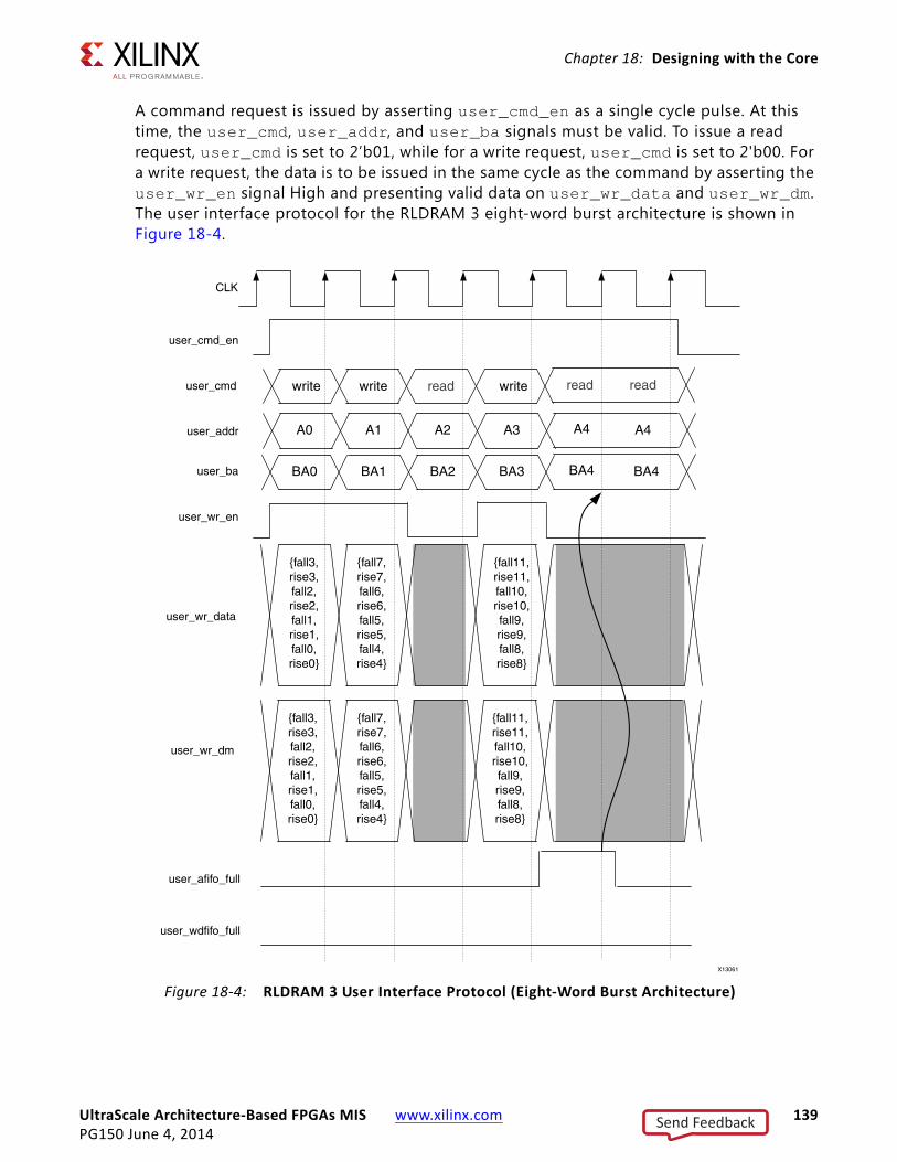
UltraScale Architecture-Based FPGAs MIS www.xilinx.com 139PG150 June 4, 2014
Chapter 18: Designing with the Core
A command request is issued by asserting user_cmd_en as a single cycle pulse. At this time, the user_cmd, user_addr, and user_ba signals must be valid. To issue a read request, user_cmd is set to 2’b01, while for a write request, user_cmd is set to 2'b00. For a write request, the data is to be issued in the same cycle as the command by asserting the user_wr_en signal High and presenting valid data on user_wr_data and user_wr_dm. The user interface protocol for the RLDRAM 3 eight-word burst architecture is shown in Figure 18-4.
X-Ref Target - Figure 18-4
Figure 18-4: RLDRAM 3 User Interface Protocol (Eight-Word Burst Architecture)
Send Feedback
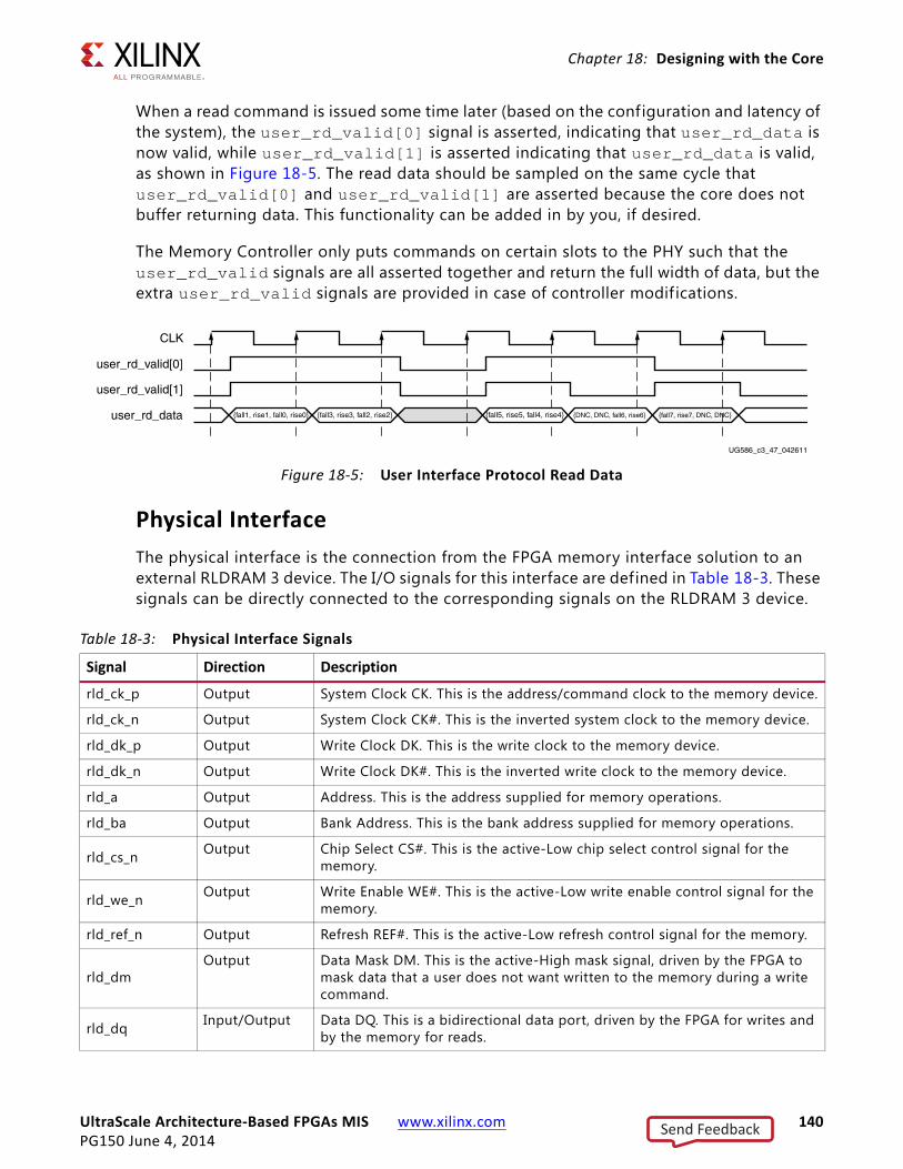
UltraScale Architecture-Based FPGAs MIS www.xilinx.com 140PG150 June 4, 2014
Chapter 18: Designing with the Core
When a read command is issued some time later (based on the configuration and latency of the system), the user_rd_valid[0] signal is asserted, indicating that user_rd_data is now valid, while user_rd_valid[1] is asserted indicating that user_rd_data is valid, as shown in Figure 18-5. The read data should be sampled on the same cycle that user_rd_valid[0] and user_rd_valid[1] are asserted because the core does not buffer returning data. This functionality can be added in by you, if desired.
The Memory Controller only puts commands on certain slots to the PHY such that the user_rd_valid signals are all asserted together and return the full width of data, but the extra user_rd_valid signals are provided in case of controller modif ications.
Physical InterfaceThe physical interface is the connection from the FPGA memory interface solution to an external RLDRAM 3 device. The I/O signals for this interface are defined in Table 18-3. These signals can be directly connected to the corresponding signals on the RLDRAM 3 device.
X-Ref Target - Figure 18-5
Figure 18-5: User Interface Protocol Read Data
Table 18-3: Physical Interface Signals
Signal Direction Description
rld_ck_p Output System Clock CK. This is the address/command clock to the memory device.
rld_ck_n Output System Clock CK#. This is the inverted system clock to the memory device.
rld_dk_p Output Write Clock DK. This is the write clock to the memory device.
rld_dk_n Output Write Clock DK#. This is the inverted write clock to the memory device.
rld_a Output Address. This is the address supplied for memory operations.
rld_ba Output Bank Address. This is the bank address supplied for memory operations.
rld_cs_n Output Chip Select CS#. This is the active-Low chip select control signal for the memory.
rld_we_n Output Write Enable WE#. This is the active-Low write enable control signal for the memory.
rld_ref_n Output Refresh REF#. This is the active-Low refresh control signal for the memory.
rld_dmOutput Data Mask DM. This is the active-High mask signal, driven by the FPGA to
mask data that a user does not want written to the memory during a write command.
rld_dq Input/Output Data DQ. This is a bidirectional data port, driven by the FPGA for writes and by the memory for reads.
Send Feedback
UltraScale Architecture-Based FPGAs MIS www.xilinx.com 141PG150 June 4, 2014
Chapter 18: Designing with the Core
rld_qk_pInput Read Clock QK. This is the read clock returned from the memory edge aligned
with read data on rld_dq. This clock (in conjunction with QK#) is used by the PHY to sample the read data on rld_dq.
rld_qk_nInput Read Clock QK#. This is the inverted read clock returned from the memory.
This clock (in conjunction with QK) is used by the PHY to sample the read data on rld_dq.
rld_reset_n Output RLDRAM 3 reset pin. This is the active-Low reset to the RLDRAM 3 device.
Table 18-3: Physical Interface Signals (Cont’d)
Signal Direction Description
Send Feedback

UltraScale Architecture-Based FPGAs MIS www.xilinx.com 142PG150 June 4, 2014
Chapter 19
Design Flow StepsThis chapter describes customizing and generating the core, constraining the core, and the simulation, synthesis and implementation steps that are specific to this IP core. More detailed information about the standard Vivado® design flows in the Vivado IP integrator can be found in the following Vivado Design Suite user guides:
• Vivado Design Suite User Guide: Designing IP Subsystems using IP Integrator (UG994) [Ref 5]
• Vivado Design Suite User Guide: Designing with IP (UG896) [Ref 6]
• Vivado Design Suite User Guide: Getting Started (UG910) [Ref 7]
• Vivado Design Suite User Guide: Logic Simulation (UG900) [Ref 8]
Customizing and Generating the CoreThis section includes information about using Xilinx® tools to customize and generate the core in the Vivado Design Suite.
If you are customizing and generating the core in the IP integrator, see the Vivado Design Suite User Guide: Designing IP Subsystems using IP Integrator (UG994) [Ref 5] for detailed information. IP integrator might auto-compute certain configuration values when validating or generating the design. To check whether the values change, see the description of the parameter in this chapter. To view the parameter value, run the validate_bd_design command in the Tcl Console.
You can customize the IP for use in your design by specifying values for the various parameters associated with the IP core using the following steps:
1. Select the IP from the IP catalog.
2. Double-click the selected IP or select the Customize IP command from the toolbar or right-click menu.
For details, see the Vivado Design Suite User Guide: Designing with IP (UG896) [Ref 6] and the Vivado Design Suite User Guide: Getting Started (UG910) [Ref 7].
Send Feedback
UltraScale Architecture-Based FPGAs MIS www.xilinx.com 143PG150 June 4, 2014
Chapter 19: Design Flow Steps
MIG I/O PlanningFor details on I/O planning, see MIG I/O Planning, page 58.
User ParametersTable 19-1 shows the relationship between the GUI f ields in the Vivado IDE and the User Parameters (which can be viewed in the Tcl Console).
Output GenerationFor details, see the Vivado Design Suite User Guide: Designing with IP (UG896) [Ref 6].
Constraining the CoreThis section contains information about constraining the core in the Vivado Design Suite.
Required ConstraintsThis section is not applicable for this IP core.
Table 19-1: GUI Parameter to User Parameter RelationshipGUI Parameter/Value(1) User Parameter/Value(1) Default Value
System Clock Configuration System_Clock Differential
Internal VREF Internal_Vref TRUE
DCI_Cascade FALSE
Debug Signal for Controller Debug_Signal Disable
Clock 1 (MHz) ADDN_UI_CLKOUT1_FREQ_HZ None
Clock 2 (MHz) ADDN_UI_CLKOUT2_FREQ_HZ None
Clock 3 (MHz) ADDN_UI_CLKOUT3_FREQ_HZ None
Clock 4 (MHz) ADDN_UI_CLKOUT4_FREQ_HZ None
Clock Period (ps) C0.RLD3_TimePeriod 1,071
Input Clock Period (ps) C0.RLD3_InputClockPeriod 13,947
Fabric to Memory Clock Ratio C0.RLD3_PhyClockRatio 4:1
Configuration C0.RLD3_MemoryType Components
Memory Part C0.RLD3_MemoryPart MT44K16M36RB-093
Data Width C0.RLD3_DataWidth 36
Data Mask C0.RLD3_DataMask TRUE
Burst Length C0.RLD3_BurstLength 81. Parameter values are listed in the table where the GUI parameter value differs from the user parameter value. Such
values are shown in this table as indented below the associated parameter.
Send Feedback
UltraScale Architecture-Based FPGAs MIS www.xilinx.com 144PG150 June 4, 2014
Chapter 19: Design Flow Steps
Device, Package, and Speed Grade SelectionsThis section is not applicable for this IP core.
Clock FrequenciesThis section is not applicable for this IP core.
Clock ManagementFor more information on clocking, see Clocking, page 127.
Clock PlacementThis section is not applicable for this IP core.
BankingThis section is not applicable for this IP core.
Transceiver PlacementThis section is not applicable for this IP core.
I/O Standard and PlacementThe MIG tool generates the appropriate I/O standards and placement based on the selections made in the Vivado IDE for the interface type and options.
IMPORTANT: The set_input_delay and set_output_delay constraints are not needed on the external memory interface pins in this design due to the calibration process that automatically runs at start-up. Warnings seen during implementation for the pins can be ignored.
SimulationThis section contains information about simulating IP in the Vivado Design Suite. For comprehensive information about Vivado simulation components, as well as information about using supported third-party tools, see the Vivado Design Suite User Guide: Logic Simulation (UG900) [Ref 8].
Send Feedback
UltraScale Architecture-Based FPGAs MIS www.xilinx.com 145PG150 June 4, 2014
Chapter 19: Design Flow Steps
Synthesis and ImplementationThis section contains information about synthesis and implementation in the Vivado Design Suite. For details about synthesis and implementation, see the Vivado Design Suite User Guide: Designing with IP (UG896) [Ref 6].
Send Feedback

UltraScale Architecture-Based FPGAs MIS www.xilinx.com 146PG150 June 4, 2014
Chapter 20
Example DesignThis chapter contains information about the example design provided in the Vivado® Design Suite.
Vivado supports Open IP Example Design flow. To create the example design using this flow, right-click the IP in the Source Window, as shown in Figure 20-1 and select Open IP Example Design.
This option creates a new Vivado project. Upon selecting the menu, a dialog box to enter the directory information for the new design project opens.
Select a directory, or use the defaults, and click OK. This launches a new Vivado with all of the example design f iles and a copy of the IP. This project has example_top as the Implementation top directory and sim_tb_top as the Simulation top directory, as shown in Figure 20-2.
X-Ref Target - Figure 20-1
Figure 20-1: Open IP Example Design
Send Feedback

UltraScale Architecture-Based FPGAs MIS www.xilinx.com 147PG150 June 4, 2014
Chapter 20: Example Design
Simulating the Example Design (Designs with Standard User Interface)The example design provides a synthesizable test bench to generate a f ixed simple data pattern to the Memory Controller. This test bench consists of an IP wrapper and an example_tb that generates 10 writes and 10 reads. Memory model f iles are not generated when designs are generated from the IP. You need to download memory models from the Micron® website.
IMPORTANT: Xilinx® UNISIMS_VER and SECUREIP library must be mapped into the simulator.
To run the simulation, go to this directory:
<project_dir>/example_project/<Component_Name>example/<Component_Name>_example.srcs/sim_1/imports/<Component_Name>/tb
X-Ref Target - Figure 20-2
Figure 20-2: Example Design Project
Send Feedback
UltraScale Architecture-Based FPGAs MIS www.xilinx.com 148PG150 June 4, 2014
Chapter 20: Example Design
If the MIG design is generated with the Component Name entered in the Vivado IDE as mig_0, the simulation directory path is the following:
<project_dir>/example_project/mig_0_example/mig_0_example.srcs/sim_1/imports/mig_0/tb
Copy the memory models in the above directory and see the readme.txt f ile located in the folder for running simulations.
The Questa® SIM simulation tool is used for verif ication of MIG IP at each software release. Script f ile to run simulations with Questa SIM is generated in MIG generated output. MIG designs are not verif ied with Vivado Simulator. Other simulation tools can be used for MIG IP simulation but are not specifically verif ied by Xilinx.
Send Feedback
UltraScale Architecture-Based FPGAs MIS www.xilinx.com 149PG150 June 4, 2014
Chapter 21
Test BenchThis chapter contains information about the test bench provided in the Vivado® Design Suite.
The Memory Controller is generated along with a simple test bench to verify the basic read and write operations. The stimulus contains 10 consecutive writes followed by 10 consecutive reads for data integrity check.
Send Feedback
UltraScale Architecture-Based FPGAs MIS www.xilinx.com 150PG150 June 4, 2014
SECTION V: APPENDICES
Debugging
Additional Resources and Legal Notices
Send Feedback
UltraScale Architecture-Based FPGAs MIS www.xilinx.com 151PG150 June 4, 2014
Appendix A
DebuggingThis appendix includes details about resources available on the Xilinx® Support website and debugging tools.
TIP: If the IP generation halts with an error, there might be a license issue. See License Checkers in Chapter 1 for more details.
Finding Help on Xilinx.comTo help in the design and debug process when using the MIS, the Xilinx Support web page (www.xilinx.com/support) contains key resources such as product documentation, release notes, answer records, information about known issues, and links for opening a Technical Support WebCase.
DocumentationThis product guide is the main document associated with the MIS. This guide, along with documentation related to all products that aid in the design process, can be found on the Xilinx Support web page (www.xilinx.com/support) or by using the Xilinx Documentation Navigator.
Download the Xilinx Documentation Navigator from the Design Tools tab on the Downloads page (www.xilinx.com/download). For more information about this tool and the features available, open the online help after installation.
Solution CentersSee the Xilinx Solution Centers for support on devices, software tools, and intellectual property at all stages of the design cycle. Topics include design assistance, advisories, and troubleshooting tips.
The Solution Center specif ic to the MIS core is located at Xilinx MIG Solution Center.
Send Feedback
UltraScale Architecture-Based FPGAs MIS www.xilinx.com 152PG150 June 4, 2014
Appendix A: Debugging
Answer RecordsAnswer Records include information about commonly encountered problems, helpful information on how to resolve these problems, and any known issues with a Xilinx product. Answer Records are created and maintained daily ensuring that users have access to the most accurate information available.
Answer Records for this core can be located by using the Search Support box on the main Xilinx support web page. To maximize your search results, use proper keywords such as:
• Product name
• Tool message(s)
• Summary of the issue encountered
A filter search is available after results are returned to further target the results.
Master Answer Record for the MIS
AR: 58435
Contacting Technical SupportXilinx provides technical support at www.xilinx.com/support for this LogiCORE™ IP product when used as described in the product documentation. Xilinx cannot guarantee timing, functionality, or support of product if implemented in devices that are not defined in the documentation, if customized beyond that allowed in the product documentation, or if changes are made to any section of the design labeled DO NOT MODIFY.
To contact Xilinx Technical Support:
1. Navigate to www.xilinx.com/support.
2. Open a WebCase by selecting the WebCase link located under Additional Resources.
When opening a WebCase, include:
• Target FPGA including package and speed grade.
• All applicable Xilinx Design Tools and simulator software versions.
• Additional f iles based on the specif ic issue might also be required. See the relevant sections in this debug guide for guidelines about which f ile(s) to include with the WebCase.
Note: Access to WebCase is not available in all cases. Log in to the WebCase tool to see your specif ic support options.
Send Feedback
UltraScale Architecture-Based FPGAs MIS www.xilinx.com 153PG150 June 4, 2014
Appendix A: Debugging
Debug ToolsThere are many tools available to address MIS design issues. It is important to know which tools are useful for debugging various situations.
Vivado Lab ToolsVivado® lab tools insert logic analyzer and virtual I/O cores directly into your design. Vivado lab tools also allow you to set trigger conditions to capture application and integrated block port signals in hardware. Captured signals can then be analyzed. This feature in the Vivado IDE is used for logic debugging and validation of a design running in Xilinx devices.
The Vivado logic analyzer is used with the logic debug IP cores, including:
• ILA 2.0 (and later versions)
• VIO 2.0 (and later versions)
See the Vivado Design Suite User Guide: Programming and Debugging (UG908) [Ref 10].
Hardware DebugHardware issues can range from link bring-up to problems seen after hours of testing. This section provides debug steps for common issues. The Vivado lab tools are a valuable resource to use in hardware debug. The signal names mentioned in the following individual sections can be probed using the Vivado lab tools for debugging the specif ic problems.
General ChecksEnsure that all the timing constraints for the core were properly incorporated from the example design and that all constraints were met during implementation.
• If using MMCMs in the design, ensure that all MMCMs have obtained lock by monitoring the locked port.
• If your outputs go to 0, check your licensing.
• If you are experiencing issues with DDR3 or DDR4 interfaces, run the following Tcl Console commands in the Vivado when connected to the hardware:
refresh_hw_device [lindex [get_hw_devices] 0]
report_property [lindex [get_hw_migs] 0]
Send Feedback
UltraScale Architecture-Based FPGAs MIS www.xilinx.com 154PG150 June 4, 2014
Appendix A: Debugging
• Copy all of the data reported and submit it as part of a WebCase. For more information on opening a WebCase, see the Contacting Technical Support, page 152.
Send Feedback
UltraScale Architecture-Based FPGAs MIS www.xilinx.com 155PG150 June 4, 2014
Appendix B
Additional Resources and Legal Notices
Xilinx ResourcesFor support resources such as Answers, Documentation, Downloads, and Forums, see Xilinx Support.
For a glossary of technical terms used in Xilinx® documentation, see the Xilinx Glossary.
ReferencesThese documents provide supplemental material useful with this product guide:
1. JESD79-3F, DDR3 SDRAM Standard and JESD79-4, DDR4 SDRAM Standard, JEDEC® Solid State Technology Association
2. Kintex® UltraScale™ Architecture Data Sheet: DC and AC Switching Characteristics (DS892)
3. UltraScale Architecture SelectIO™ Resources User Guide (UG571)
4. UltraScale Architecture PCB Design and Pin Planning User Guide (UG583)
5. Vivado® Design Suite User Guide: Designing IP Subsystems using IP Integrator (UG994)
6. Vivado Design Suite User Guide: Designing with IP (UG896)
7. Vivado Design Suite User Guide: Getting Started (UG910)
8. Vivado Design Suite User Guide: Logic Simulation (UG900)
9. Vivado Design Suite User Guide: Implementation (UG904)
10. Vivado Design Suite User Guide: Programming and Debugging (UG908)
11. ISE® to Vivado Design Suite Migration Guide (UG911)
Send Feedback
UltraScale Architecture-Based FPGAs MIS www.xilinx.com 156PG150 June 4, 2014
Appendix B: Additional Resources and Legal Notices
Revision HistoryThe following table shows the revision history for this document.
Date Version Revision
06/04/2014 5.0 • Removed PCB sections and added link to UG583.• Global replace BUFGCE to BUFGCE_DIV.DDR3/DDR4• Updated CAS cycle description in DDR3 Feature Summary.• Updated descriptions in Native Interface section.• Updated Control Path section.• Updated Read and Write Coalescing section.• Updated Reordering section.• Updated DDR4 x16 parts in Group Machines section.• Updated Fig. 3-3: PHY Block Diagram.• Updated Table 3-1: PHY Modules.• Updated module names in Overall PHY Architecture section.• Updated Fig. 3-4: PHY Overall Initialization and Calibration Sequence.• Added description to Memory Initialization and Calibration Sequence
section.• Added SSI rule in Clocking section.• Added SSI rule and updated Address and ck descriptions in DDR3/DDR4
Pin Rules sections.• Added Important Note for calibration stage in DDR3/DDR4 Pinout
Examples sections.• Updated signal descriptions in Table 4-3: User Interface.• Added new content in app_addr[ADDR_WIDTH – 1:0] section.• Updated Write Path section.• Updated Native Interface section.• Added Important Note relating to Data Mask in Controller Options section.• Updated Fig. 5-1 to 5-8 in Customizing and Generating the Core section.• Added User Parameters section in Design Flow Steps chapter.• Updated I/O Standard and Placement section.• Added Synplify Black Box Testing section in Example Design chapter.
Continued
QDR II+• Updated Read Latency in Feature Summary section.• Updated Fig. 10-2: PHY Block Diagram and Table 17-1: PHY Modules.• Updated Table 11-2: User Interface.• Added SSI rule in Clocking section.• Added Important Note for calibration stage in QDR II+ Pinout Examples
section.• Added SSI rule in QDR II+ Pin Rules section.• Updated I/O Standard and Placement section.• Added User Parameters section in Design Flow Steps chapter.
Send Feedback
UltraScale Architecture-Based FPGAs MIS www.xilinx.com 157PG150 June 4, 2014
Appendix B: Additional Resources and Legal Notices
Continued
• Updated the descriptions in Simulating the Example Design (Designs with Standard User Interface) section.
• Added Synplify Black Box Testing section in Example Design chapter.
RLDRAM 3• Added 18 bits in Feature Summary section.• Updated Fig. 17-4: PHY Block Diagram.• Updated module names in Table 17-1: PHY Modules.• Updated module names in Overall PHY Architecture section.• Added SSI rule in Clocking section.• Updated c) and d) descriptions and added SSI rule in RLDRAM 3 Pin Rules
section.• Updated Table 18-2: User Interface Request Signals.• Updated Fig. 18-2: Multiple Commands for user_cmd Signal.• Added Important Note for calibration stage in RLDRAM 3 Pinout Examples
section.• Updated I/O Standard and Placement section.• Added User Parameters section in Design Flow Steps chapter.• Updated Test Bench chapter.
04/02/2014 5.0 • Added Verilog Test Bench in IP Facts table.DDR3/DDR4• Added Overview chapter.• Updated component support to 80 bits in Feature Summary section.• Updated DDR Device Utilization tables.• Updated DDR Clocking section.• Updated x4 DRAM to Four Component DRAM Configuration in Designing
with the Core chapter.• Updated Important note in PCB Guidelines for DDR3 and DDR4 Overview
sections.• Updated Important note in Reference Stack-Up for DDR3 and DDR4
sections.• Updated trace length descriptions in DDR3 and DDR4 sections.• Added VTT Terminations guideline in Generic Routing Guideline for DDR3
and DDR4 sections.• Updated all descriptions in Limitations section.• Added VREF note in Required Constraints section.• Updated new figures in Design Flow Steps chapter.• Added new descriptions in Example Design chapter.• Added new description in Test Bench chapter.QDR II+ SRAM• Added new QDR II section.RLDRAM 3• Added Overview chapter.• Added new Clocking section.• Added new descriptions in Example Design chapter.
Date Version Revision
Send Feedback

UltraScale Architecture-Based FPGAs MIS www.xilinx.com 158PG150 June 4, 2014
Appendix B: Additional Resources and Legal Notices
Please Read: Important Legal NoticesThe information disclosed to you hereunder (the "Materials") is provided solely for the selection and use of Xilinx products. To the maximum extent permitted by applicable law: (1) Materials are made available "AS IS" and with all faults, Xilinx hereby DISCLAIMS ALL WARRANTIES AND CONDITIONS, EXPRESS, IMPLIED, OR STATUTORY, INCLUDING BUT NOT LIMITED TO WARRANTIES OF MERCHANTABILITY, NON-INFRINGEMENT, OR FITNESS FOR ANY PARTICULAR PURPOSE; and (2) Xilinx shall not be liable (whether in contract or tort, including negligence, or under any other theory of liability) for any loss or damage of any kind or nature related to, arising under, or in connection with, the Materials (including your use of the Materials), including for any direct, indirect, special, incidental, or consequential loss or damage (including loss of data, profits, goodwill, or any type of loss or damage suffered as a result of any action brought by a third party) even if such damage or loss was reasonably foreseeable or Xilinx had been advised of the possibility of the same. Xilinx assumes no obligation to correct any errors contained in the Materials or to notify you of updates to the Materials or to product specifications. You may not reproduce, modify, distribute, or publicly display the Materials without prior written consent. Certain products are subject to the terms and conditions of Xilinx's limited warranty, please refer to Xilinx's Terms of Sale which can be viewed at http://www.xilinx.com/legal.htm#tos; IP cores may be subject to warranty and support terms contained in a license issued to you by Xilinx. Xilinx products are not designed or intended to be fail-safe or for use in any application requiring fail-safe performance; you assume sole risk and liability for use of Xilinx products in such critical applications, please refer to Xilinx's Terms of Sale which can be viewed at http://www.xilinx.com/legal.htm#tos.© Copyright 2013–2014 Xilinx, Inc. Xilinx, the Xilinx logo, Artix, ISE, Kintex, Spartan, UltraScale, Virtex, Vivado, Zynq, and other designated brands included herein are trademarks of Xilinx in the United States and other countries. All other trademarks are the property of their respective owners.
ContinuedAppendix• Updated Debug Appendix.
12/18/2013 4.2 Initial Xilinx release.
Date Version Revision
Send Feedback


![UltraScale Architecture SelectIO Resourcesxilinx.eetrend.com/files-eetrend-xilinx/download/201408/...UltraScale Architecture and Product Overview (DS890) [Ref 2] documents the available](https://static.fdocuments.in/doc/165x107/60e45cee86db48053717ec31/ultrascale-architecture-selectio-ultrascale-architecture-and-product-overview.jpg)