Xilinx FPGAs:Evolution and Revolution. Evolution results in bigger, faster, cheaper FPGAs; better...
45
Xilinx FPGAs:Evolution and Revolution
-
Upload
clifton-storrs -
Category
Documents
-
view
232 -
download
4
Transcript of Xilinx FPGAs:Evolution and Revolution. Evolution results in bigger, faster, cheaper FPGAs; better...

Xilinx FPGAs:Evolution and Revolution

Evolution results in bigger, faster, cheaper FPGAs; better software with fewer bugs, faster compile times; coupled with better technical support.

Innovative architectural and circuit features with advancements in design methodology - modular team based design & internet based configuration method: resulting in Revolution.

A Decade of Progress
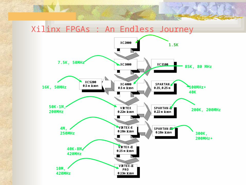
Xilinx FPGAs : An Endless JourneyXC2000
XC40000.5 micron
XC3100
VIRTEX0.22micron
VIRTEX-E0.18micron
XC3000
XC52000.5 micron SPARTAN
0.35, 0.25 m
VIRTEX-II0.15 micron
VIRTEX-IIPRO
0.13micron
SPARTAN-II0.22 micron
SPARTAN-IIE0.18micron
1.5K
7.5K, 50MHz85K, 80 MHz
100MHz+40K
16K, 50MHz
50K-1M,200MHz 200K, 200MHz
4M,250MHz 300K,
200MHz+
40K-8M,420MHz
10M,420MHz
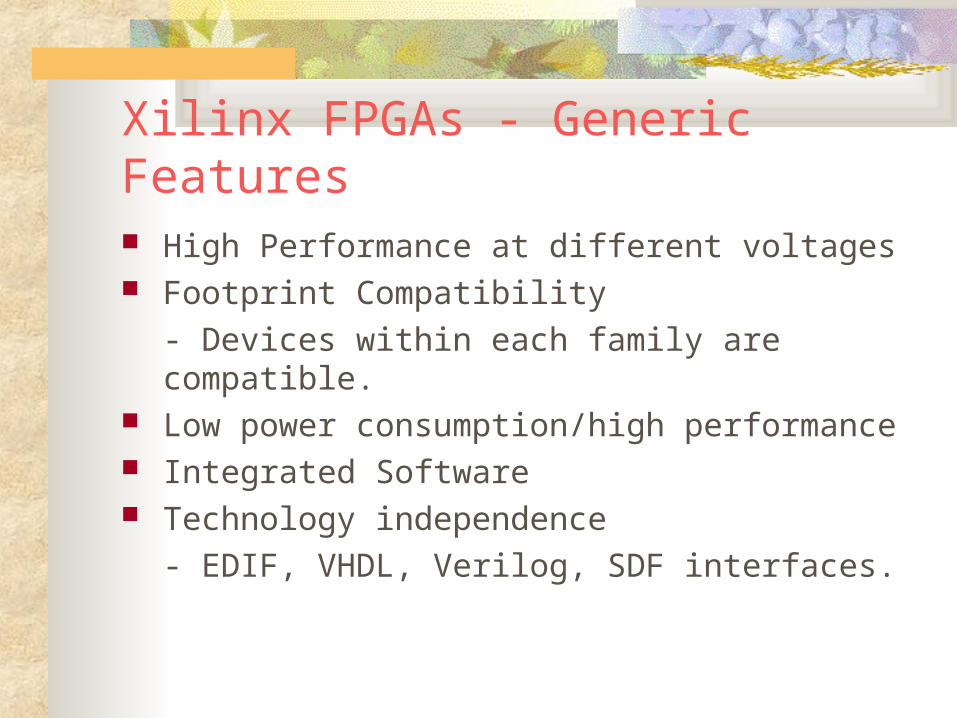
Xilinx FPGAs - Generic Features High Performance at different voltages Footprint Compatibility
- Devices within each family are compatible. Low power consumption/high performance Integrated Software Technology independence
- EDIF, VHDL, Verilog, SDF interfaces.

XC2000 First FPGA Family from Xilinx. Two members:
XC2064 1000 Gates
XC2018 1500 Gates Ext. Crystal Oscillator. No Tri State Buffers. XACT 1.0 Development System.

XC2000 Max.Logic Gates 1500 Max. CLB Flip-flop 100 Max. I/O Pins 74 Max. I/O Flip-Flop 74

XC3000 Replaces TTL, MSI and other PLD logics. Integrates complete subsystem into single
Package. System clock Speed up to 50 MHz. On-chip crystal Oscillator. Low-Skew Clock Nets. Over 20 different Packaging Options Interface to popular design Environment like
Mentor, Cadence and View Logic.

XC3000 CLB
XC3100A Ultra-high-speed Family with six members. XC3195 in 22 X 22 CLB array size. Compatible with XC3000. Error checking of configuration bit stream.

XC4000 CLB

XC4000 Family Features Synchronous Single and Dual-Port RAM Internal Three-state buffers. JTAG Boundary Scan System performance to 80 MHz 0.5 µ SRAM Process Technology

XC4000 Sub-FamiliesVersion Max. logic Max. I/O Voltage
Gates
XC4000XL 3k-85k 448 3.3
XC4000EX 28k, 36k 320 5
XC4000E 3.0-25k 256 5

XC5200 Low Cost FPGA Family. System Features:
- Fast Arithmetic Functions- High Performance Clock Network- Highly routable- Easy Pin Locking- Fast wide Functions- Three-state buffers- JTAG- Performance up to 50 MHz.

Resource Comparison

Xilinx 4000 Series
Heritage
Total Cost Management
Advanced ProcessTechnology
Small die size
Low cost packaging Low test cost
100 MHz+ performanceOn-chip SelectRAMSoftware v4.2iCore solutions
Xilinx Spartan/XL FPGAs

Total Cost Management
Leading edge process technology Smallest die size of any FPGA with on-chip RAM
Focused package offering Low-power architecture allows use of highest volume
plastic packages Streamlined test flow
Lower cost test hardware Built-in self test features and shorter test times
Optimized manufacturing flows

Chip
Combines 3.3 V operation with 0.25u benefits
Spartan-XL Family Advanced 0.35m Process
Transistor gates 0.35u Allows 3.3 V supply
All other features 0.25u Small size
Low capacitance Performance

Spartan Speed GradesPe
rform
ance
XC5200 XC4000E Spartan Spartan-XL
E-1
E-2
-4
-3
-4
-3
XL-5
XL-4
Higher speed grade = higher performance
What’s missing in Spartan?
No asynchronous RAM Only RAM16(32)X1S, RAM16X1D, ROM16X1
No edge decoders No DECODEx
No wired-AND No WANDx or WOR2AND
Mode pins not usable as I/O No MD0, MD1, MD2
Virtex - features Densities from 50 K to 1M system gates. System performance up to 200 MHz. Multi-standard Select IO interfaces. Built-in clock-management circuitry
- Four DLLs
- Four Low-skew global Clock Distribution Net Hierarchical Memory System. Dedicated Multiplier Support.

Spartan-II - features Densities as high as 200K gates. Streamlined features based on Virtex architecture. Very Low Cost LUT Distributed RAM and Block RAM support. Dedicated Multiplier support. 4 DLLs

Virtex/Spartan-II CLB 1 CLB holds 2 slices Each slice has two sets of
Four-input LUT Any 4-input logic function Or 16-bit x 1 RAM Or 16-bit shift register
Carry & Control Fast arithmetic logic Multiplier logic Multiplexer logic
Storage element Latch or flip-flop Set and reset True or inverted inputs Sync. or Async. Control
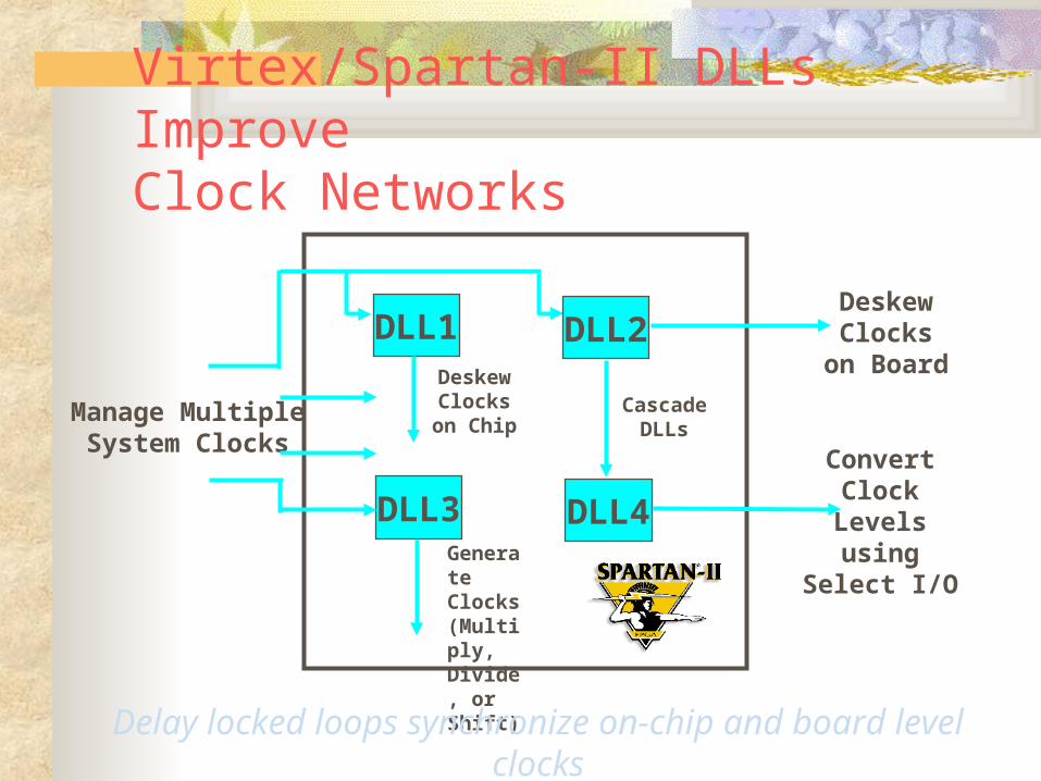
Virtex/Spartan-II DLLs ImproveClock Networks
DLL1
DLL3
DeskewClockson Chip
Manage MultipleSystem Clocks
DeskewClocks
on Board
CascadeDLLs
GenerateClocks (Multiply, Divide, or Shift)
ConvertClockLevelsusing
Select I/O
Delay locked loops synchronize on-chip and board level clocks
DLL4
DLL2

Virtex-E – what’s added? Up to 4 million system gates 2-4X more Block RAM 8 DLLs Differential I/O signaling (LVDS/BLVDS) some new speed grades.
Spartan-IIE - features Density 50-300K Supports LVDS 4 DLLs VCCINT – 1.8V More speed grades than Spartan-II. Less packaging Options.

Virtex-II All Xilinx FPGAs contain the same basic resources
CLBs contain combinatorial logic and register resources IOBs interface between the FPGA and the outside world Programmable interconnect Other resources
Three-state buffers Global clock buffers Boundary scan logic
Virtex-II devices contain additional resources Block SelectRAM Dedicated Multipliers Digital Clock Manager (DCM)

CLB Tile
CIN
SwitchMatrix
TBUFTBUF
COUTCOUT
Slice S0
Slice S1
Fast Connects
Slice S2
Slice S3
CIN
SHIFT

Slice Structure
Slice 0
LUT Carry
LUT Carry D QCE
PRE
CLR
D QCE
PRE
CLR

Mult-AND and dedicated Multiplier too SRL16 DDR Registers. Fast Carry Logic Digitally Controlled Impedance
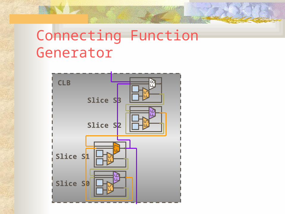
Connecting Function Generator
F5F8
F5F6
CLB
Slice S3
Slice S2
Slice S0
Slice S1 F5F7
F5F6

Select I/O
Allows direct connections to external signals of varied voltages and thresholds Optimizes the speed/noise tradeoff Saves having to place interface components onto your
board Differential signaling standards
LVDS, BLVDS, ULVDS LDT

Distributed and Block Select RAM
RAM16X1S
O
D
WE
WCLK
A0
A1
A2
A3
LUT
RAM32X1S
O
D
WE
WCLK
A0
A1
A2
A3
A4
RAM16X1D
SPO
D
WE
WCLK
A0
A1
A2
A3
DPRA0 DPO
DPRA1
DPRA2
DPRA3
Slice
LUT
LUT
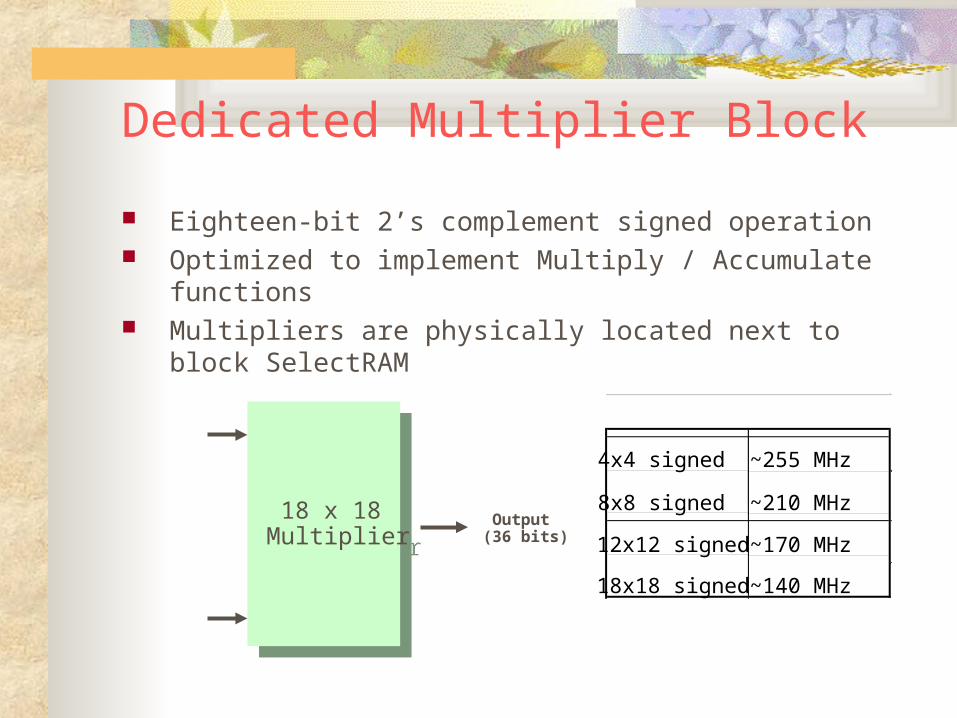
Dedicated Multiplier Block
18 x 18 Multiplier
18 x 18 Multiplier
Output (36 bits)
4x4 signed ~255 MHz
8x8 signed ~210 MHz
12x12 signed ~170 MHz
18x18 signed ~140 MHz
Eighteen-bit 2’s complement signed operation Optimized to implement Multiply / Accumulate functions Multipliers are physically located next to block SelectRAM

DCM
Up to twelve DCMs per device Located on top and bottom edges of the die Driven by clock input pads
DCMs provide: Delay-Locked Loop (DLL) Digital Frequency Synthesizer (DFS) Digital Phase Shifter (DPS) Digital Spread Spectrum (DSS)
Up to four outputs of each DCM can drive onto global clock buffers All DCM outputs can drive general routing

Challenges to accelerate Processing performance
Multiple TasksMultiple Tasks
Parallel Processing in Hardware
Multiple Processors on Multiple Tasks
Multiple Solutions
• High performance• lower cost • low complexity
• Specific task focus• Scalable
Parallel Processing Using
Multiple Processors
Very Large Single Task
requires Parallel
Processing
Typesof
Challenges
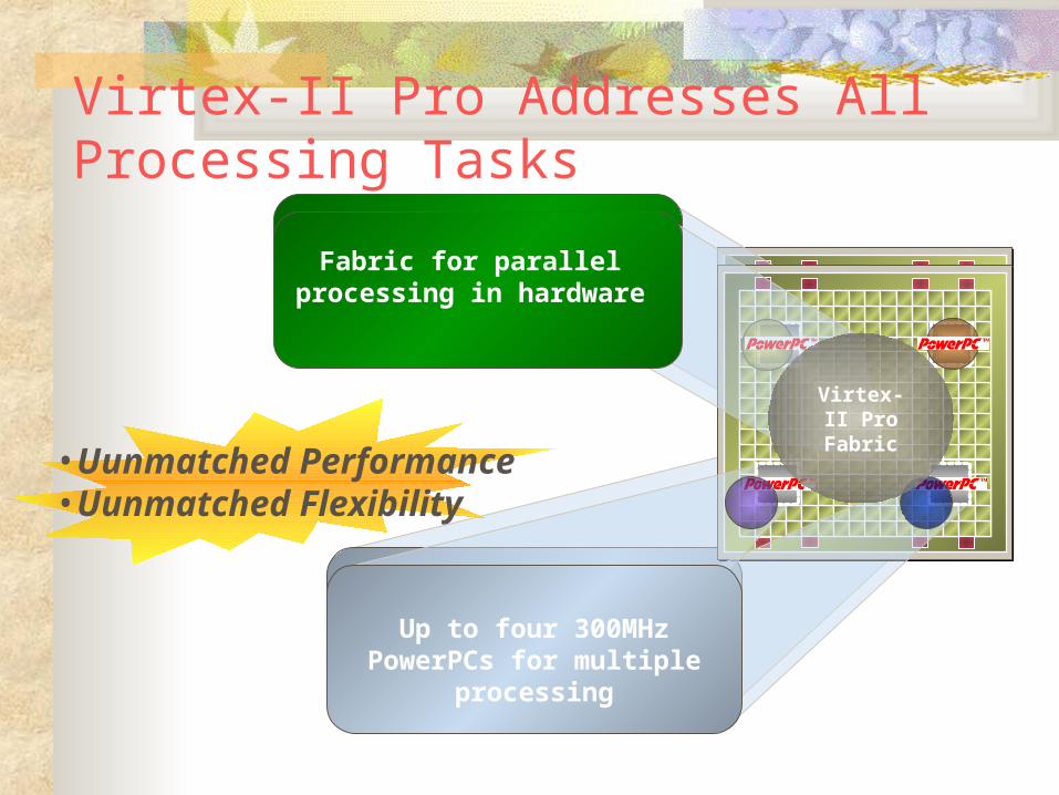
Virtex-II Pro Addresses All Processing Tasks
Up to four 300MHz PowerPCs for multiple processing
Virtex-II Pro Fabric
Fabric for parallel processing in hardware
Up to four 300MHz PowerPCs for multiple processing
•Uunmatched Performance•Uunmatched Flexibility
Virtex-II Pro Fabric
Fabric for parallel processing in hardware

Logic Capacity and Features

Virtex II Pro Leads all the way

Supply Voltage XC4000 and Spartan families use a 5V supply. The-XL families use 3.3 V supply. Virtex and Spartan-II use 2.5V supply. Virtex-E uses 1.8 V. Virtex-II and Virtex-IIPro uses 1.5 V

Xilinx Development System
XACT 1.0; 2.0 ... 6.0
Xilinx-NeoCADMerge
M 1.0
M2.0i....M5.1i

THE FUTURE……. In 2005, FPGAs will be built on 70nm-Cu
process; will implement 50 million system gates; with 2 billion transistors on-chip; with 10 layers of copper metal; with embedded processors running at 1 GHz clock rate; with direct interface to 10 Gbps serial data.

URLs www.xilinx.com www.fpga-faq.com www.optimagic.com www.datasheetlocator.com Newsgroup comp.arch.fpga