
XDPL8219 design guide - Infineon Technologies
51
Design Guide Please read the Important Notice and Warnings at the end of this document V 1.0 www.infineon.com/XDPL8219 page 1 of 51 2020-06-17 DG_2005_PL21_2006_124819 XDPL8219 design guide For high power factor flyback converter with constant voltage output About this document Scope and purpose This document is a design guide using XDPL8219 as the control IC of the front-stage high power factor (HPF) flyback converter, which regulates the secondary output voltage supply to the second-stage constant current (CC) converter for LED lighting applications. Intended audience This design guide is intended for power supply design engineers and field application engineers. Table of contents About this document ....................................................................................................................... 1 Table of contents ............................................................................................................................ 1 1 Introduction .......................................................................................................................... 3 2 Design specifications .............................................................................................................. 5 3 Transformer design ................................................................................................................ 6 4 Flyback MOSFET and secondary main output diode selection ...................................................... 8 5 CS resistor and GD pin-related design ...................................................................................... 10 6 Input voltage parameters for operation, start-up and protection ............................................... 11 7 HV pin-related design ............................................................................................................ 12 8 DC link filter and secondary output capacitance ....................................................................... 13 9 VCC capacitance and VCC self-supply circuit ................................................................................ 14 10 Pre-start-up check and start-up phase..................................................................................... 15 11 Output UVP-related design ..................................................................................................... 16 12 Output OVP-related design ..................................................................................................... 17 13 ZCD pin and input voltage sensing related design ..................................................................... 18 14 Secondary-side regulation FB circuit design ............................................................................. 20 15 Regulated mode parameters .................................................................................................. 23 15.1 Digital notch filter.................................................................................................................................. 23 15.2 Initial feedback voltage maximum limit............................................................................................... 23 15.3 Regulated mode CS pin maximum voltage and minimum QRMn valley number limits .................... 24 15.4 On-time limits ........................................................................................................................................ 25 15.5 ABM FB voltage sensing and control .................................................................................................... 26 15.6 Filtered FB voltage mapping and mode transition .............................................................................. 27 16 UART reporting ..................................................................................................................... 29 17 Other functions and protections ............................................................................................. 32 17.1 Enhanced power factor correction ....................................................................................................... 32 17.2 Enhanced THD correction ..................................................................................................................... 32
Transcript of XDPL8219 design guide - Infineon Technologies

Design Guide Please read the Important Notice and Warnings at the end of this document V 1.0
www.infineon.com/XDPL8219 page 1 of 51 2020-06-17
DG_2005_PL21_2006_124819
XDPL8219 design guide
For high power factor flyback converter with constant voltage output
About this document
Scope and purpose
This document is a design guide using XDPL8219 as the control IC of the front-stage high power factor (HPF) flyback converter, which regulates the secondary output voltage supply to the second-stage constant current (CC) converter for LED lighting applications.
Intended audience
This design guide is intended for power supply design engineers and field application engineers.
Table of contents
About this document ....................................................................................................................... 1
Table of contents ............................................................................................................................ 1
1 Introduction .......................................................................................................................... 3
2 Design specifications .............................................................................................................. 5
3 Transformer design ................................................................................................................ 6
4 Flyback MOSFET and secondary main output diode selection ...................................................... 8
5 CS resistor and GD pin-related design ...................................................................................... 10
6 Input voltage parameters for operation, start-up and protection ............................................... 11
7 HV pin-related design ............................................................................................................ 12
8 DC link filter and secondary output capacitance ....................................................................... 13
9 VCC capacitance and VCC self-supply circuit ................................................................................ 14
10 Pre-start-up check and start-up phase ..................................................................................... 15
11 Output UVP-related design ..................................................................................................... 16
12 Output OVP-related design ..................................................................................................... 17
13 ZCD pin and input voltage sensing related design ..................................................................... 18
14 Secondary-side regulation FB circuit design ............................................................................. 20
15 Regulated mode parameters .................................................................................................. 23
15.1 Digital notch filter .................................................................................................................................. 23 15.2 Initial feedback voltage maximum limit ............................................................................................... 23 15.3 Regulated mode CS pin maximum voltage and minimum QRMn valley number limits .................... 24 15.4 On-time limits ........................................................................................................................................ 25
15.5 ABM FB voltage sensing and control .................................................................................................... 26
15.6 Filtered FB voltage mapping and mode transition .............................................................................. 27
16 UART reporting ..................................................................................................................... 29
17 Other functions and protections ............................................................................................. 32 17.1 Enhanced power factor correction ....................................................................................................... 32
17.2 Enhanced THD correction ..................................................................................................................... 32

Design Guide 2 of 51 V 1.0
2020-06-17
XDPL8219 design guide For high power factor flyback converter with constant voltage output
Introduction
17.3 Switching frequency dithering for constant DC input ......................................................................... 32 17.4 Auto restart time ................................................................................................................................... 32
17.5 VCC OVP ................................................................................................................................................... 32 17.6 Regulated mode VCC UVP ....................................................................................................................... 33
17.7 IC overtemperature protection ............................................................................................................. 33 17.8 Primary MOSFET over-current protection ............................................................................................ 33
17.9 Debug mode .......................................................................................................................................... 33
18 PCB layout guide ................................................................................................................... 34
19 Parameter configuration list, setup and procedures ................................................................. 35 19.1 Parameter configuration list ................................................................................................................. 35 19.2 Parameter configuration setup ............................................................................................................ 36
19.3 Parameter configuration procedures ................................................................................................... 37
20 Fine-tuning guide .................................................................................................................. 40
20.1 Input voltage-sensing parameter fine-tuning ...................................................................................... 40 20.2 QR valley switching parameter fine-tuning .......................................................................................... 41 20.3 Power factor related parameter fine-tuning ........................................................................................ 43 20.4 THD related parameter fine-tuning ...................................................................................................... 43
21 Debugging guide ................................................................................................................... 45 21.1 UART reporting error code readout ...................................................................................................... 46
21.2 Debug mode error code readout by test configuration ....................................................................... 47 21.3 Debug mode error code readout by burn configuration ..................................................................... 48
22 References ........................................................................................................................... 49
23 Revision history .................................................................................................................... 50
Design Guide 3 of 51 V 1.0
2020-06-17
XDPL8219 design guide For high power factor flyback converter with constant voltage output
Introduction
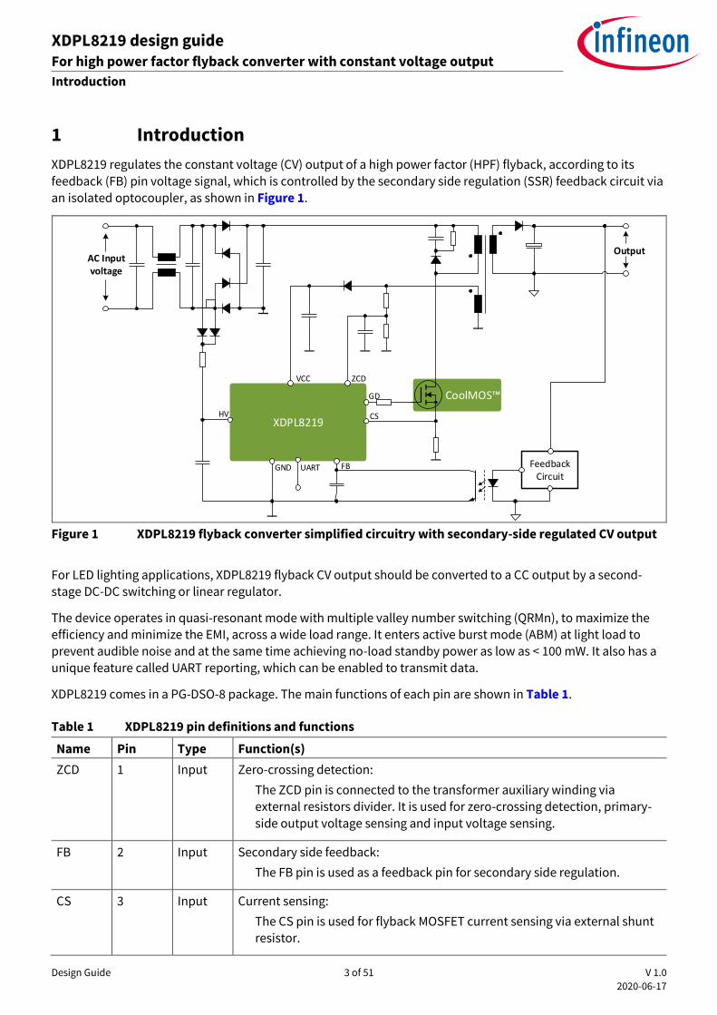
1 Introduction
XDPL8219 regulates the constant voltage (CV) output of a high power factor (HPF) flyback, according to its
feedback (FB) pin voltage signal, which is controlled by the secondary side regulation (SSR) feedback circuit via an isolated optocoupler, as shown in Figure 1.
CoolMOS
XDPL8219
Feedback Circuit
VCC
CS
GD
ZCD
Output
HV
FB GND UART
AC Inputvoltage
Figure 1 XDPL8219 flyback converter simplified circuitry with secondary-side regulated CV output
For LED lighting applications, XDPL8219 flyback CV output should be converted to a CC output by a second-stage DC-DC switching or linear regulator.
The device operates in quasi-resonant mode with multiple valley number switching (QRMn), to maximize the efficiency and minimize the EMI, across a wide load range. It enters active burst mode (ABM) at light load to prevent audible noise and at the same time achieving no-load standby power as low as < 100 mW. It also has a unique feature called UART reporting, which can be enabled to transmit data.
XDPL8219 comes in a PG-DSO-8 package. The main functions of each pin are shown in Table 1.
Table 1 XDPL8219 pin definitions and functions
Name Pin Type Function(s)
ZCD 1 Input Zero-crossing detection:
The ZCD pin is connected to the transformer auxiliary winding via external resistors divider. It is used for zero-crossing detection, primary-
side output voltage sensing and input voltage sensing.
FB 2 Input Secondary side feedback:
The FB pin is used as a feedback pin for secondary side regulation.
CS 3 Input Current sensing:
The CS pin is used for flyback MOSFET current sensing via external shunt
resistor.

Design Guide 4 of 51 V 1.0
2020-06-17
XDPL8219 design guide For high power factor flyback converter with constant voltage output
Introduction
Name Pin Type Function(s)
GD 4 Output Gate driver:
The GD pin is used for flyback MOSFET gate drive control via external series resistor.
HV 5 Input High voltage:
The HV pin is connected to the rectified input voltage via external series resistor. The HV pin is used to charge VCC pin voltage during start-up and
protection, via an internal 600 V start-up cell. In addition, it is also used for line synchronization.
UART 6 Input
/Output
Universal asynchronous receiver transmitter (UART):
The UART pin is used as the digital interface for IC parameter
configuration. It can also be used for the information reporting based on the uni-directional UART communication (when UART reporting is enabled).
VCC 7 Input Operating voltage supply and sensing
GND 8 – IC grounding
Note: By default, the configurable parameters of a new XDPL8219 chip from Infineon are empty, so it is
necessary to configure them before any application testing.
Figure 2 shows the XDPL8219 design guide document sectioning for each step of the recommended design flow.
Figure 2 XDPL8219 design guide document sectioning for each step of the recommended design
flow
XDPL8219 system design
(Refer section 2 to 18)
Create system based on system design
(Refer section 19 for IC parameterization setup
and procedures)
Power up system
(If any problem, refer section 21 for
debugging guide)
Performance check and optimization
(Refer section 20 for fine-tuning
guide)

Design Guide 5 of 51 V 1.0
2020-06-17
XDPL8219 design guide For high power factor flyback converter with constant voltage output
Design specifications
2 Design specifications
A front-stage HPF flyback converter with CV output set-point Vout,setpoint of 54 V (54 V/0.8 A) has been selected as a
design example. The design specifications are shown in Table 2.
Table 2 Design specifications
Specification Symbol Value Unit
Normal operational minimum AC input voltage VAC,min 90 Vrms
Normal operational maximum AC input voltage VAC,max 305 Vrms
Normal operational AC input frequency Fline 47 ~ 63 Hz
Secondary-side regulated CV output set-point Vout,setpoint 54 V
Steady-state output load current Iout 0 ~ 800 mA
Steady-state full-load output power Pout,full 43.2 W
Minimum efficiency at Pout,full ƞmin,at,P,out,full 90 %
Target minimum switching frequency at Pout,full fsw,min,at,P,out,full 52 kHz
Note: Pout,full of 43.2 W is defined in this design example, to be able to supply a second-stage CC converter
which has minimum efficiency of 93 percent (or maximum 3.2 W loss) at full load, for a 40 W LED driver
design.
Note: The recommended fsw,min,at,P,out,full is between 45 kHz and 65 kHz. In general, higher fsw,min,at,P,out,full value would result in a smaller flyback transformer with lower efficiency, while lower fsw,min,at,P,out,full value
would result in a larger flyback transformer with higher efficiency.

Design Guide 6 of 51 V 1.0
2020-06-17
XDPL8219 design guide For high power factor flyback converter with constant voltage output
Transformer design
3 Transformer design
To achieve both high efficiency and high power quality in the quasi-resonant valley switching operation, the
flyback transformer primary main winding to secondary main winding turns ratio, N, should be high enough, but without exceeding the flyback MOSFET drain-source breakdown voltage V(BR)DSS. Based on the VAC,max
requirement of 305 Vrms, MOSFET V(BR)DSS = 800 V is selected for a good price to performance ratio.
To reduce transformer leakage inductance for low MOSFET voltage spike Vspike,FET, transformer design with sandwich construction as shown in Figure 3 is recommended. Additionally, with the primary RCD snubber network deployed across the primary main winding (see Figure 1), Vspike,FET can be estimated to be around 30
percent to 45 percent of VAC,max as a rule of thumb. In this design example, VAC,max is 305 Vrms, so we simply
assume Vspike,FET = 100 V, which is approximately 33 percent of VAC,max.
Figure 3 Transformer design with sandwich construction
For good reliability against input voltage surge, it is recommended to reserve a voltage margin Vmargin,FET of
minimum 50 V from V(BR)DSS. If XDPL8219 input overvoltage protection (OVP) would be enabled later in Section 6, as a rule of thumb, Vmargin,FET should be at least 25 percent of VAC,max, which is equivalent to 76.25 V based on VAC,max of 305 Vrms. In this design example, Vmargin,FET = 90 V is selected.
Based on the above, N can be defined as:
𝑁 ≤ 𝑉(𝐵𝑅)𝐷𝑆𝑆 − 𝑉𝐴𝐶,𝑚𝑎𝑥(𝑝𝑘) − 𝑉𝑠𝑝𝑖𝑘𝑒,𝐹𝐸𝑇 − 𝑉𝑚𝑎𝑟𝑔𝑖𝑛,𝐹𝐸𝑇
𝑉𝑜𝑢𝑡,𝑠𝑒𝑡𝑝𝑜𝑖𝑛𝑡 + 𝑉𝑑 (1)
Where VAC,max(pk) is √2 times VAC,max, and Vd is the secondary main output diode forward voltage.
Taking Vd = 0.7 V, N can then be calculated as:
𝑁 ≤ 800 − √2 ∙ 305 − 100 − 90
54 + 0.7 = 3.27
Based on the above, N = 3.2 is selected.
The maximum primary peak current Ipri(pk),max can then be defined and calculated as:
𝐼𝑝𝑟𝑖(𝑝𝑘),𝑚𝑎𝑥 ≈ 4 ∙ 𝑃𝑜𝑢𝑡,𝑓𝑢𝑙𝑙
ƞ𝑚𝑖𝑛,𝑎𝑡,𝑃,𝑜𝑢𝑡,𝑓𝑢𝑙𝑙 ∙ [
1
𝑁 ∙ (𝑉𝑜𝑢𝑡,𝑠𝑒𝑡𝑝𝑜𝑖𝑛𝑡+ 𝑉𝑑) +
1
𝑉𝐴𝐶,𝑚𝑖𝑛(𝑝𝑘)] (2)
Where VAC,min(pk) is √2 times VAC,min.
𝐼𝑝𝑟𝑖(𝑝𝑘),𝑚𝑎𝑥 ≈ 4 ∙ 43.2
90% ∙ [
1
3.2 ∙ (54 + 0.7) +
1
√2 ∙ 90]
𝑰𝒑𝒓𝒊(𝒑𝒌),𝒎𝒂𝒙 ≈ 𝟐. 𝟔𝟎𝟔 𝑨

Design Guide 7 of 51 V 1.0
2020-06-17
XDPL8219 design guide For high power factor flyback converter with constant voltage output
Transformer design
As a result, the primary main winding inductance Lp can be defined and calculated as:
𝐿𝑝 = 𝑉𝐴𝐶,𝑚𝑖𝑛(𝑝𝑘) ∙ 𝑁 ∙ (𝑉𝑜𝑢𝑡,𝑠𝑒𝑡𝑝𝑜𝑖𝑛𝑡 + 𝑉𝑑)
𝐼𝑝𝑟𝑖(𝑝𝑘),𝑚𝑎𝑥 ∙ 𝑓𝑠𝑤,𝑚𝑖𝑛,𝑎𝑡,𝑃,𝑜𝑢𝑡,𝑓𝑢𝑙𝑙 ∙ [𝑉𝐴𝐶,𝑚𝑖𝑛(𝑝𝑘)+ 𝑁 ∙ (𝑉𝑜𝑢𝑡,𝑠𝑒𝑡𝑝𝑜𝑖𝑛𝑡+ 𝑉𝑑)] (3)
𝐿𝑝 = √2 ∙ 90 ∙ 3.2 ∙ (54 + 0.7)
2.606 ∙ 52 ∙ 103 ∙ [√2 ∙ 90 + 3.2 ∙ (54 + 0.7)]
𝑳𝒑 = 𝟓𝟒𝟒 𝝁𝑯
Based on core cross-sectional area, Ae = 120.1 mm2 and saturation flux density at 100°C, Bsat(T=100°C) = 0.41 Tesla for TDG PQ26/20 core with TPW33 material, the transformer primary main winding turns Np can be defined as:
𝑁𝑝 ≥ 𝐿𝑝 ∙ 𝐼𝑝𝑟𝑖(𝑝𝑘),𝑚𝑎𝑥
𝐴𝑒 ∙ 𝐵𝑠𝑎𝑡(𝑇=100°𝐶) ∙ 𝐷𝑓,𝐵𝑠𝑎𝑡 (4)
Where Df,Bsat is the derating factor to ensure the designed transformer maximum flux density Bmax is below
Bsat(T=100°C) by a margin of (100 percent - Df,Bsat) from saturation, and it is typical to set Df,Bsat in the range of 85 percent to 95 percent for a margin of 5 percent to 15 percent from transformer core saturation.
Taking Df,Bsat = 90 percent, Np can then be calculated as:
𝑁𝑝 ≥ 544 ∙ 10−6 ∙ 2.606
120.1 ∙ 10−6 ∙ 0.41 ∙ 90% = 31.99
Based on the above, Np = 32 is selected.
The transformer secondary main winding turns Ns can then be calculated as:
𝑁𝑠 = 𝑁𝑝
𝑁 =
32
3.2
𝑵𝒔 = 𝟏𝟎
To ensure fast VCC supply takeover from the primary auxiliary winding for avoiding IC reset during start-up, and
also to be able to deliver peak gate-drive voltage VGD,peak of 12 V with high enough primary auxiliary winding VCC
supply during steady-state, the minimum primary auxiliary winding demagnetization voltage Va,min = 14 V is
therefore defined. As a result, the recommended minimum primary auxiliary winding turns Na,min can be defined and calculated as:
𝑁𝑎,𝑚𝑖𝑛 =𝑉𝑎,𝑚𝑖𝑛 ∙ 𝑁𝑠
(𝑉𝑜𝑢𝑡,𝑠𝑒𝑡𝑝𝑜𝑖𝑛𝑡 + 𝑉𝑑)=
14 ∙ 10
(54 + 0.7)= 2.56 (5)
To minimize the IC power consumption and, VCC voltage should not exceed 19 V, the maximum auxiliary winding demagnetization voltage Va,max = 19 is therefore defined. As a result, the recommended maximum primary auxiliary winding turns Na,max can be defined and calculated as:
𝑁𝑎,𝑚𝑎𝑥 =𝑉𝑎,𝑚𝑎𝑥 ∙ 𝑁𝑠
(𝑉𝑜𝑢𝑡,𝑠𝑒𝑡𝑝𝑜𝑖𝑛𝑡 + 𝑉𝑑)=
19 ∙ 10
(54 + 0.7)= 3.47 (6)
Based on the calculation results of equations (5) and (6), primary auxiliary winding turns Na = 3 is selected.
A secondary auxiliary winding is added to supply the operating voltage of the secondary side regulation (SSR)
FB circuit, since its op-amp or shunt regulator’s maximum operating voltage is less than Vout,setpoint of 54 V. The recommended minimum secondary auxiliary winding turns Na,sec,min and recommended maximum secondary auxiliary winding turns Na,sec,max can be defined respectively as per Na,min and Na,max, as shown below:
𝑁𝑎,𝑠𝑒𝑐,𝑚𝑖𝑛 = 𝑁𝑎,𝑚𝑖𝑛 = 2.56 (7)
𝑁𝑎,𝑠𝑒𝑐,𝑚𝑎𝑥 = 𝑁𝑎,𝑚𝑎𝑥 = 3.47 (8)
Based on the calculation results of equations (7) and (8), secondary auxiliary winding turns Na,sec = 3 is selected.

Design Guide 8 of 51 V 1.0
2020-06-17
XDPL8219 design guide For high power factor flyback converter with constant voltage output
Flyback MOSFET and secondary main output diode selection
4 Flyback MOSFET and secondary main output diode selection
The CoolMOSTM P7 MOSFET series is the latest CoolMOSTM product family and targets customers looking for high
performance and at the same time being price sensitive. Through optimizing key parameters (Coss, Eoss, QG, Ciss and VGS(th)); integrating Zener diode for ESD protection and other measures, this product family fully addresses
market concerns in performance, ease-of-use, and price/performance ratio, delivering best-in-class performance with exceptional ease-of-use, while still not compromising on price/performance ratio. The 700 V and 800 V types of the CoolMOSTM P7 series have been designed for flyback and could also be used in PFC
topologies.
MOSFET drain-source breakdown voltage V(BR)DSS = 800 V is selected in this design example based on VAC,max of 305 Vrms and transformer design in Section 3.
Before selecting which MOSFET drain-source on-resistance at room temperature Rds(on),25°C is to be used, the maximum primary rms current Ipri(rms),max has to be estimated based on:
𝐼𝑝𝑟𝑖(𝑟𝑚𝑠),𝑚𝑎𝑥 ≈ 𝐼𝑝𝑟𝑖(𝑝𝑘),𝑚𝑎𝑥 ∙ √𝑘
3 (9)
Where k is a number obtained from the function curve in Figure 4, based on the variable factor of 𝑉𝐴𝐶,𝑚𝑖𝑛(𝑝𝑘)
𝑁 ∙ (𝑉𝑜𝑢𝑡,𝑠𝑒𝑡𝑝𝑜𝑖𝑛𝑡+ 𝑉𝑑) .
In this design example, the variable factor of 𝑉𝐴𝐶,𝑚𝑖𝑛(𝑝𝑘)
𝑁 ∙ ( 𝑉𝑜𝑢𝑡,𝑠𝑒𝑡𝑝𝑜𝑖𝑛𝑡+ 𝑉𝑑) can be calculated as:
𝑉𝐴𝐶,𝑚𝑖𝑛(𝑝𝑘)
𝑁 ∙ (𝑉𝑜𝑢𝑡,𝑠𝑒𝑡𝑝𝑜𝑖𝑛𝑡+ 𝑉𝑑) =
√2 ∙ 90
3.2 ∙ ( 54 + 0.7)= 0.727
Referring to the function curve in Figure 4, k = 0.31 is obtained.
Based on equation (9), Ipri(rms),max can then be calculated as:
𝐼𝑝𝑟𝑖(𝑟𝑚𝑠),𝑚𝑎𝑥 ≈ 2.606 ∙ √0.31
3
𝑰𝒑𝒓𝒊(𝒓𝒎𝒔),𝒎𝒂𝒙 ≈ 𝟎. 𝟖𝟑𝟖 𝑨
Figure 4 Function curve of k

Design Guide 9 of 51 V 1.0
2020-06-17
XDPL8219 design guide For high power factor flyback converter with constant voltage output
Flyback MOSFET and secondary main output diode selection
The selectable MOSFET Rds(on),25°C can be defined as:
𝑅𝑑𝑠(𝑜𝑛),25°𝐶 ≤ 𝑚 ∙ 𝑃𝑜𝑢𝑡,𝑓𝑢𝑙𝑙
𝐼𝑝𝑟𝑖(𝑟𝑚𝑠),𝑚𝑎𝑥2 ∙ ∆𝑅𝑑𝑠(𝑜𝑛),100°𝐶
(10)
Where m is the desired ratio of MOSFET conduction loss over Pout,full and ∆Rds(on),100°C is the ratio of 𝑅𝑑𝑠(𝑜𝑛),100°𝐶
𝑅𝑑𝑠(𝑜𝑛),25°𝐶.
It is typical to select m in the range of 0.025 to 0.03 and ∆Rds(on),100°C in the range of 1.75 to 1.85. Taking m = 0.0275 and ∆Rds(on),100°C = 1.8, Rds(on),25°C can then be calculated as:
𝑅𝑑𝑠(𝑜𝑛),25°𝐶 ≤ 0.0275 ∙ 43.2
0.8382 ∙ 1.8 = 0.94 Ω
Referring to the calculation results of equation (10) and Table 3 below, Rds(on),25°C = 900 mΩ is selected.
To utilize the PCB as a heatsink for the MOSFET, IPD80R900P7 with TO-252 (DPAK) package is selected.
Table 3 800 V CoolMOSTM P7 selection table
For the secondary main output diode selection, it is necessary to first estimate the maximum reverse voltage
Vr(diode),max and maximum secondary main winding peak current Isec(pk),max, based on:
𝑉𝑟(𝑑𝑖𝑜𝑑𝑒),𝑚𝑎𝑥 = 𝑉𝑠𝑝𝑖𝑘𝑒,𝑑𝑖𝑜𝑑𝑒 + 𝑉𝑜𝑢𝑡,𝑠𝑒𝑡𝑝𝑜𝑖𝑛𝑡 + 𝑉𝐴𝐶,𝑚𝑎𝑥(𝑝𝑘)+ 𝑉𝑚𝑎𝑟𝑔𝑖𝑛,𝐹𝐸𝑇
𝑁 (11)
Where Vspike,diode is the diode reverse voltage spike.
Assuming 𝑉𝑠𝑝𝑖𝑘𝑒,𝑑𝑖𝑜𝑑𝑒 ≈ 35% ∙ (𝑉𝑜𝑢𝑡,𝑠𝑒𝑡𝑝𝑜𝑖𝑛𝑡 + 𝑉𝐴𝐶,𝑚𝑎𝑥(𝑝𝑘)+ 𝑉𝑚𝑎𝑟𝑔𝑖𝑛,𝐹𝐸𝑇
𝑁),
𝑉𝑟(𝑑𝑖𝑜𝑑𝑒),𝑚𝑎𝑥 ≈ 135% ∙ (𝑉𝑜𝑢𝑡,𝑠𝑒𝑡𝑝𝑜𝑖𝑛𝑡 + 𝑉𝐴𝐶,𝑚𝑎𝑥(𝑝𝑘)+ 𝑉𝑚𝑎𝑟𝑔𝑖𝑛,𝐹𝐸𝑇
𝑁) = 135% ∙ (54 +
√2 ∙ 305 + 90
3.2)
𝑉𝑟(𝑑𝑖𝑜𝑑𝑒),𝑚𝑎𝑥 ≈ 292.81 𝑉
𝐼𝑠𝑒𝑐(𝑝𝑘),𝑚𝑎𝑥 ≈ 𝐼𝑝𝑟𝑖(𝑝𝑘),𝑚𝑎𝑥 ∙ 𝑁𝑝
𝑁𝑠 = 2.606 ∙
32
10 (12)
𝐼𝑠𝑒𝑐(𝑝𝑘),𝑚𝑎𝑥 ≈ 8.34 𝐴
Based on the above, a secondary main output diode with repetitive reverse voltage rating VRRM = 300 V is selected. To minimize its switching and conduction losses, the selected diode also has the properties of hyper-fast recovery speed and low forward voltage drop at Isec(pk),max.
Additionally, a RC secondary snubber network, e.g., 10 Ω resistor in series with 150 pF capacitor, is
deployed across the secondary main output diode, to suppress the diode reverse voltage spike and the EMI.

Design Guide 10 of 51 V 1.0
2020-06-17
XDPL8219 design guide For high power factor flyback converter with constant voltage output
CS resistor and GD pin-related design
5 CS resistor and GD pin-related design
Figure 5 shows the connections of the current sense (CS) resistor RCS, gate resistor RG and gate source resistor
RGS.
CS
RCS
GD
RGS
RG
Figure 5 GD pin, CS pin, RCS, RG and RGS connections
Based on the CS pin voltage across RCS, the MOSFET current can be measured.
The recommended minimum CS resistor value RCS,min is defined and calculated as:
𝑅𝐶𝑆,𝑚𝑖𝑛 =0.45
𝐼𝑝𝑟𝑖(𝑝𝑘),𝑚𝑎𝑥=
0.45
2.606= 0.173 Ω (13)
The recommended maximum CS resistor value RCS,max is defined and calculated as:
𝑅𝐶𝑆,𝑚𝑎𝑥 =0.54
𝐼𝑝𝑟𝑖(𝑝𝑘),𝑚𝑎𝑥=
0.54
2.606= 0.207 Ω (14)
Based on the calculation results above, CS resistor RCS = 0.2 Ω is selected in this design example.
RG is to damp the gate-rise oscillation, and RGS is to ensure the MOSFET gate has relatively low impedance to
prevent it from being switched on undesirably. RG = 10 Ω and RGS = 20 kΩ are selected in this design example.
The gate-drive peak voltage VGD,pk is typically 12 V with sufficient VCC voltage supply. To achieve a good balance
of switching loss and EMI, the gate voltage rising slope can be controlled by configuring the gate driver peak
source current parameter IGD,pk (configurable range: 30 mA to 118 mA). This saves two components (see Dfastoff, Rslowon in Figure 6), which are conventionally added for the same purpose.
t
VGD
IGD,pk
= 30mA
=118mA
(12V typ.)
IGD,pk
VGD,pk
Figure 6 Gate-drive voltage rising slope control with IGD,pk parameterization for component saving
With the high-speed switching characteristics of CoolMOSTM P7 MOSFET, it is recommended to configure the IGD,pk parameter in the range of 30 mA to 49 mA.
As a result, IGD,pk = 30 mA is selected in this design example.

Design Guide 11 of 51 V 1.0
2020-06-17
XDPL8219 design guide For high power factor flyback converter with constant voltage output
Input voltage parameters for operation, start-up and protection
6 Input voltage parameters for operation, start-up and
protection
The lowest operational input voltage parameter Vin,low and the highest operational input voltage parameter Vin,high can be defined and calculated as:
𝑉𝑖𝑛,𝑙𝑜𝑤 = 𝑎 ∙ 𝑉𝐴𝐶,𝑚𝑖𝑛 (15)
𝑉𝑖𝑛,ℎ𝑖𝑔ℎ = 𝑏 ∙ 𝑉𝐴𝐶,𝑚𝑎𝑥 (16)
Where a is recommended to be between 0.9 and 0.95, and b is recommended to be between 1.05 and 1.10.
Taking a = 0.91 and b = 1.07,
𝑽𝒊𝒏,𝒍𝒐𝒘 = 𝟖𝟐 𝑽𝒓𝒎𝒔
𝑽𝒊𝒏,𝒉𝒊𝒈𝒉 = 𝟑𝟐𝟔 𝑽𝒓𝒎𝒔
ENOVP,In parameter refers to the enable switch for maximum input voltage start-up check and input OVP, based
on Vin,start,max and VinOV levels, respectively. ENOVP,In = Enabled is selected in this design example.
ENUVP,In parameter refers to the enable switch for minimum input voltage start-up check and input UVP, based
on Vin,start,min and VinUV levels, respectively. ENUVP,In = Enabled is selected in this design example.
Vin,start,max parameter refers to the maximum input voltage level setting for start-up, which is recommended to be
configured as Vin,high. Hence, Vin,start,max = 326 Vrms is selected in this design example. VinOV parameter refers to the input OVP level setting, which is recommended to be:
𝑉𝑖𝑛𝑂𝑉 ≥ 𝑉𝑖𝑛,𝑠𝑡𝑎𝑟𝑡,𝑚𝑎𝑥 ∙ 107% = 349 𝑉𝑟𝑚𝑠 (17)
Vin,start,min parameter refers to the minimum input voltage level setting for start-up, which is recommended to be
configured as Vin,low. Hence, Vin,start,min = 82 Vrms is selected in this design example. VinUV parameter refers to the input UV (brown-out) protection level setting, which is recommended as:
𝑉𝑖𝑛𝑈𝑉 ≤ 𝑉𝑖𝑛,𝑠𝑡𝑎𝑟𝑡,𝑚𝑖𝑛 ∙ 93% = 76 𝑉𝑟𝑚𝑠 (18)
Based on the above, VinOV = 350 Vrms and VinUV = 70 Vrms are selected in this design example.
The input voltage protections (based on VinOV and VinUV) in ABM can be optionally enabled with ENVIN,ABM
parameter. If ENVIN,ABM is enabled, the enable switches for VinOV and VinUV protections in ABM are respectively
based on ENOVP,In and ENUVP,In. In this design example, ENVIN,ABM = Enabled is selected. The input OVP blanking
period number parameter tVinOV,blank = 1 is recommended and selected in this design example.
Vin
t
VinOV
Vin,start,max
VinUV
Vin,start,min
Startup
Startup
Startup
Protectiontriggered
Protection triggered
Figure 7 Input voltage levels for start-up and protection (with auto restart reaction)

Design Guide 12 of 51 V 1.0
2020-06-17
XDPL8219 design guide For high power factor flyback converter with constant voltage output
HV pin-related design
7 HV pin-related design
As shown in Figure 8, HV series resistor RHV is connected from the HV pin to the cathodes of HV diode DHV1 and
DHV2, while bridge rectifier AC input should be applied across the DHV1 anode and DHV2 anode.
A high voltage capacitor CHV should also be connected between the HV pin and ground, to filter the switching
noise for a robust HV pin line synchronization. In addition, CHV also improves the input voltage surge and ESD capability of the HV pin.
The repetitive reverse voltage rating VRRM = 1000 V for DHV1 and DHV2 is recommended and selected in this design example, to ensure good reliability of the diodes against input voltage surge.
RHV
HV
~ ~
CHV
DHV1 DHV2
Bridge rectifier`
Figure 8 HV pin, RHV, CHV, DHV1 and DHV2 connections
The recommended minimum HV series resistor value RHV,min is defined and calculated as:
𝑅𝐻𝑉,𝑚𝑖𝑛 =𝑉𝑖𝑛,ℎ𝑖𝑔ℎ(𝑝𝑘)
𝐼𝐻𝑉,𝑚𝑎𝑥 (19)
Where IHV,max is the HV pin maximum peak input current of 9.6 mA, and Vin,start,max(pk) is √2 times Vin,high.
𝑅𝐻𝑉,𝑚𝑖𝑛 =√2 ∙ 326
9.6 ∙ 10−3 = 48 kΩ
The recommended maximum HV series resistor value RHV,max is defined and calculated as:
𝑅𝐻𝑉,𝑚𝑎𝑥 = 𝑀𝑖𝑛 [105,𝑉𝐴𝐶,𝑚𝑖𝑛(𝑟𝑒𝑐𝑡,𝑎𝑣𝑔)− 𝑉𝑉𝐶𝐶𝑂𝑁,𝑚𝑎𝑥
𝐼𝐻𝑉,𝑚𝑖𝑛(𝑎𝑣𝑔)∙ [1 −
2
𝜋∙ 𝑠𝑖𝑛−1 (
𝑉𝑉𝐶𝐶𝑂𝑁,𝑚𝑎𝑥
𝑉𝐴𝐶,𝑚𝑖𝑛(𝑝𝑘))]] (20)
Where VAC,min(rect,avg) is the average value of the rectified VAC,min, while VVCCON,max is the maximum VCC turn-on voltage threshold of 22 V, and IHV,min(avg) is the recommended HV pin minimum average input current of 1 mA.
𝑅𝐻𝑉,𝑚𝑎𝑥 = 𝑀𝑖𝑛 [105,0.9 ∙ 90 − 22
1 ∙ 10−3 ∙ [1 −2
𝜋 ∙ 𝑠𝑖𝑛−1 (
22
√2 ∙ 90)]]
𝑅𝐻𝑉,𝑚𝑎𝑥 = 52.5 𝑘Ω
Based on the above, the HV resistor value and IC parameter setting of RHV = 52 kΩ are selected in this design
example.
The HV series resistor dielectric withstand voltage should be above the total of VAC,max(pk) and Vmargin,FET (from Section 3), which is equivalent to 521.3 V. As an example, the selected RHV = 52 kΩ in this design example can be
formed using a 36 kΩ 0.5 W resistor (dielectric withstand of 350 V) in series with a 16 kΩ 0.25 W resistor (dielectric withstand of 200 V).
CHV = 1 nF is recommended and selected in this design example.

Design Guide 13 of 51 V 1.0
2020-06-17
XDPL8219 design guide For high power factor flyback converter with constant voltage output
DC link filter and secondary output capacitance
8 DC link filter and secondary output capacitance
CDC,filter denotes the DC link filter capacitor placed after the bridge rectifier. A higher CDC,filter value gives lower EMI
but worse power quality, and vice versa.
Table 4 Recommended initial CDC,filter value
VAC,min (V) Steady-state full-load output power Pout,full (W) Recommended initial CDC,filter (𝝁F)
90 ~ 107 Less than 26 0.1
26 ~ 35 0.15
35 ~ 44 0.22
Greater than 45 Greater than 0.22
Greater than or
equal to 108
Less than 31 0.1
31 ~ 40 0.15
40 ~ 55 0.22
Greater than 55 Greater than 0.22
Referring to Table 4, initial CDC,filter = 0.22 𝝁F is selected in this design example. To improve the estimated input
voltage Vin accuracy during pre-start-up check, it is also recommended to deploy DC link resistor RDC,filter = 30 MΩ in parallel with CDC,filter, as shown in Figure 9.
AC
Input
Line Filter and
Bridge Rectifier
VDC,filter
+
-~
~
CDC,filter RDC,filter
Figure 9 CDC,filter and RDC,filter across the DC link bus voltage
Vripple,out(pk-pk),max denotes the maximum allowable secondary main output voltage peak-to-peak ripple level.
Assuming the flyback output in this design example is connected to a second-stage CC buck regulator, which has a maximum LED voltage load VLED,max of 48 V and maximum allowable duty cycle Dbuck,max of 95 percent,
Vripple,out(pk-pk),max can be defined and calculated as:
𝑉𝑟𝑖𝑝𝑝𝑙𝑒,𝑜𝑢𝑡(𝑝𝑘−𝑝𝑘),𝑚𝑎𝑥 = 2 ∙ (𝑉𝑜𝑢𝑡,𝑠𝑒𝑡𝑝𝑜𝑖𝑛𝑡 −𝑉𝐿𝐸𝐷,𝑚𝑎𝑥
𝐷𝑏𝑢𝑐𝑘,𝑚𝑎𝑥) = 2 ∙ (54 −
48
0.95) = 6.95 𝑉 (21)
The secondary main output capacitor Cout,main value can then be defined and calculated as:
𝐶𝑜𝑢𝑡,𝑚𝑎𝑖𝑛 ≥ 𝑃𝑜𝑢𝑡,𝑓𝑢𝑙𝑙
2𝜋 ∙ 𝐹𝑙𝑖𝑛𝑒,𝑚𝑖𝑛 ∙ 𝑉𝑟𝑖𝑝𝑝𝑙𝑒,𝑜𝑢𝑡(𝑝𝑘−𝑝𝑘),𝑚𝑎𝑥 ∙ 𝑉𝑜𝑢𝑡,𝑠𝑒𝑡𝑝𝑜𝑖𝑛𝑡 =
43.2
2𝜋 ∙ 47 ∙ 6.95 ∙ 54= 390 µ𝐹 (22)
Considering the electrolytic capacitor value tolerance, Cout,main = 470 𝝁F is selected in this design example.
For switching noise filtering, low-ESR ceramic capacitors Cout,main,lowESR1 = 1 𝝁F and Cout,main,lowESR2 = 0.1 𝝁F are also added in parallel with Cout,main.
The secondary auxiliary output capacitor Cout,aux,sec is recommended to be at least 47 𝜇F, to ensure stable operating voltage supply of the Secondary Side Regulation (SSR) FB circuit, during ABM.
Cout,aux,sec= 47 𝝁F is selected in this design example.

Design Guide 14 of 51 V 1.0
2020-06-17
XDPL8219 design guide For high power factor flyback converter with constant voltage output
VCC capacitance and VCC self-supply circuit
9 VCC capacitance and VCC self-supply circuit
To fulfill the typical time-to-light requirement of 500 ms, the VCC pin voltage maximum charging time for IC
activation, tVCCON,charge,max should not exceed 350 ms. Therefore, the maximum VCC capacitance CVCC,max can be defined and calculated as:
𝐶𝑉𝐶𝐶,𝑚𝑎𝑥 = 𝑉𝐴𝐶,𝑡𝑦𝑝,𝑙𝑜𝑤(𝑟𝑒𝑐𝑡,𝑎𝑣𝑔)− 𝑉𝑉𝐶𝐶𝑂𝑁,𝑚𝑎𝑥
𝑅𝐻𝑉 ∙ 𝑉𝑉𝐶𝐶𝑂𝑁,𝑚𝑎𝑥∙ 𝑡𝑉𝐶𝐶𝑂𝑁,𝑐ℎ𝑎𝑟𝑔𝑒,𝑚𝑎𝑥 ∙ [1 −
2
𝜋∙ 𝑠𝑖𝑛−1 (
𝑉𝑉𝐶𝐶𝑂𝑁,𝑚𝑎𝑥
𝑉𝐴𝐶,typ,low(𝑝𝑘))] (23)
Where VVCCON,max is the maximum VCC turn-on threshold of 22 V, VAC,typ,low(rect,avg) is the average value based on the
rectified sine wave of the lowest typical input voltage, and VAC,typ,low(pk) is the peak of the lowest typical input voltage.
Take the lowest typical input voltage VAC,typ,low as 120 Vrms in this design example,
𝐶𝑉𝐶𝐶,𝑚𝑎𝑥 = 0.9 ∙ 120 − 22
52 ∙ 103 ∙ 22∙ 350 ∙ 10−3 ∙ [1 −
2
𝜋∙ 𝑠𝑖𝑛−1 (
22
√2 ∙ 120)] = 24.13 𝜇𝐹
The VCC capacitor value and IC parameter setting of CVCC = 22 𝝁F are selected. In addition, a noise decoupling ceramic capacitor of CVCCdecouple = 0.1 𝝁F with low ESR is added in parallel to CVCC.
Typically, the CVCC and CVCCdecouple are the only capacitors needed to store the rectified auxiliary winding voltage for the VCC voltage supply. An additional capacitor Cout,aux and a blocking diode Dblock,VCC are however needed if the UART reporting feature is enabled, as shown in Figure 10, to increase the VCC hold-up time for a proper
UART reporting operation, while not increasing the tVCCON,charge,max.
Cout,aux
VCC
CVCC
Dblock,VCC
NaCVCCdecouple
Needed if XDPL8219 UART reporting is enabled with ENUART,reporting parameter
Figure 10 VCC self-supply circuit
In this design example, the UART reporting is enabled, so Dblock,VCC and Cout,aux = 220 𝝁F are added.

Design Guide 15 of 51 V 1.0
2020-06-17
XDPL8219 design guide For high power factor flyback converter with constant voltage output
Pre-start-up check and start-up phase
10 Pre-start-up check and start-up phase
Vstart,OCP1
0 2 tSS
time
Soft start phase(based on nss = 3 configuration as example)
Output charging
phase
Pre-Startup Check(e.g. input voltage,
IC temperature)
tSS tout,charge
Vout,start
Startup phase
3 tSS
VOCP1(Vin)
Start of regulation according to feedback voltage mapping
Vout
CS pin maximum voltage limit
Voltage
(0.5ms typ.) (1.0ms typ.) (1.5ms typ.)
VOCP1,init
Startup with 1st soft start step
Regulated Mode
tstart,max
Figure 11 Pre-start-up check, start-up phase and regulated mode entering
Pre-start-up check ensures the estimated input voltage Vin and IC junction temperature Tj are within the
configurable protection limits before start-up. During the pre-start-up check, the input voltage measurement switching pulse has an initial CS pin maximum voltage limit VOCP1,init, which can be defined and calculated as:
𝑉𝑂𝐶𝑃1,𝑖𝑛𝑖𝑡 = 𝑑 ∙ 𝑅𝐶𝑆 ∙ 𝑉𝐴𝐶,𝑚𝑎𝑥(𝑝𝑘) ∙ 𝑡𝑜𝑛,𝑚𝑖𝑛,𝑉,𝑖𝑛,𝑠𝑡𝑎𝑟𝑡,𝑠𝑒𝑛𝑠𝑒
𝐿𝑝 (24)
Where ton,min,V,in,start,sense is the minimum on-time for the MOSFET switching pulse to measure the input voltage
during the pre-start-up check, and d is a ratio recommended to be between 1.3 and 1.4.
Take ton,min,V,in,start,sense = 1.38 µs, and d = 1.37,
𝑉𝑂𝐶𝑃1,𝑖𝑛𝑖𝑡 = 1.37 ∙ 0.2 ∙ √2 ∙ 305 ∙ 1.38 ∙ 10−6
544 ∙ 10−6
𝑽𝑶𝑪𝑷𝟏,𝒊𝒏𝒊𝒕 = 𝟎. 𝟑 𝑽
During the start-up phase, the soft start phase is initiated and followed by the output charging phase. The soft start phase minimizes the component stress by limiting the CS pin maximum voltage for a number of steps based on nss parameter. nSS = 3 setting is recommended and selected. The output charging phase fast-charges
the estimated output voltage Vout to the Vout,start parameter value for fast VCC self-supply from the primary
auxiliary winding, with the MOSFET switching pulses based on either the CS pin maximum voltage limit of Vstart,OCP1, or the maximum on-time of ton,max(Vin), in QRMn operation.
Vstart,OCP1 and Vout,start parameters can be defined and calculated as:
𝑉𝑠𝑡𝑎𝑟𝑡,𝑂𝐶𝑃1 = 𝐼𝑝𝑟𝑖(𝑝𝑘),𝑚𝑎𝑥 ∙ 𝑅𝐶𝑆 = 2.606 ∙ 0.2 (25)
𝑽𝒔𝒕𝒂𝒓𝒕,𝑶𝑪𝑷𝟏 = 𝟎. 𝟓𝟐 𝑽
𝑉𝑜𝑢𝑡,𝑠𝑡𝑎𝑟𝑡 = 𝑉𝑎,𝑠𝑡𝑎𝑟𝑡 ∙ 𝑁𝑠
𝑁𝑎− 𝑉𝑑 (26)
Where Va,start is the desired primary auxiliary winding demagnetization voltage when output voltage is Vout,start. Va,start is recommended to be between 9 V and 10.5 V. So, taking Va,start = 9.5 V,
𝑉𝑜𝑢𝑡,𝑠𝑡𝑎𝑟𝑡 = 9.5 ∙ 10
3− 0.7
𝑽𝒐𝒖𝒕,𝒔𝒕𝒂𝒓𝒕 = 𝟑𝟏 𝑽

Design Guide 16 of 51 V 1.0
2020-06-17
XDPL8219 design guide For high power factor flyback converter with constant voltage output
Output UVP-related design
11 Output UVP-related design
In start-up phase, if the estimated output voltage Vout is lower than the Vout,start parameter level over a time-out
period of tstart,max parameter, the start-up output UVP is triggered, as shown in Figure 12 (right). tstart,max
parameter can be indirectly configured with VCC capacitance parameter CVCC, based on:
𝑡𝑠𝑡𝑎𝑟𝑡,𝑚𝑎𝑥 = 967 ∙ 𝐶𝑉𝐶𝐶 (27)
Based on the earlier selected CVCC = 22 𝜇F and equation (27), tstart,max = 21.3 ms is applied in this design example.
time
VVCC
VVCCON
VUVOFF
tout,charge
(20.5V typ.)
(6V typ.)
Vout,start
Output setpoint
tVCC,holdup
Voltage
Vout
Startup output undervoltage protection triggered
(Vout < Vout,start ,at tstart,max)
Normal startup
tstart,max
Output short startup
time
VVCC
VVCCON
VUVOFF
(20.5V typ.)
(6V typ.)
Vout,start
Output setpoint
tVCC,holdup
Voltagetstart,max
Vout
tVCCON,charge tVCCON,charge
Figure 12 Normal start-up and start-up output UVP (short) waveforms
In regulated mode, ENUVP,Vout = Enabled parameter setting is selected, to enable the regulated mode output
UVP, which can be triggered if the estimated output voltage Vout is below the regulated mode output UVP level
VoutUV for longer than a blanking time of tVoutUV,blank parameter. VoutUV parameter can be defined and calculated as:
𝑉𝑜𝑢𝑡𝑈𝑉 = 𝑉𝑎,𝑈𝑉 ∙ 𝑁𝑠
𝑁𝑎− 𝑉𝑑 (28)
Where Va,UV is the desired primary auxiliary winding demagnetization voltage when output voltage is VoutUV.
Va,UV is recommended to be between 10 V and 11 V. So, taking Va,UV = 10.1 V,
𝑉𝑜𝑢𝑡𝑈𝑉 = 10.1 ∙ 10
3− 0.7
𝑽𝒐𝒖𝒕𝑼𝑽 = 𝟑𝟑 𝑽
tVoutUV,blank is recommended to be at least 100 ms, so tVoutUV,blank = 500 ms is selected in this design example. The regulated mode output UVP reaction is configurable based on ReactionUVP,Vout parameter, so ReactionUVP,Vout =
Auto restart is selected in this design example. The start-up output UVP reaction is fixed as auto restart.
Vout
time
Turn-on
Output load current too high causing power limit and Vout drop below
set-point
Startupphase
Regulated Mode(Vout > VoutUV)
Output under-voltage protection
triggered after tVoutUV,blank VoutUV
Vout,start
Output setpointStart of regulation
according to feedback voltage mapping
Regulated Mode(Vout < VoutUV for tVoutUV,blank)
Figure 13 Regulated mode output UVP (not active in ABM)

Design Guide 17 of 51 V 1.0
2020-06-17
XDPL8219 design guide For high power factor flyback converter with constant voltage output
Output OVP-related design
12 Output OVP-related design
Under the single-fault condition of the FB pin open, the main output voltage could rise above the Vout,setpoint. As
shown in Figure 14, the output OVP would be triggered when the estimated output voltage Vout is higher than the output OVP level VoutOV for longer than a blanking time.
To prevent the output OVP from being triggered by the output overshoot during line jump, e.g., from low to
high input voltage, the output OVP level VoutOV should be configured well above Vout,setpoint. Therefore, the VoutOV parameter can be defined and calculated as:
𝑉𝑜𝑢𝑡𝑂𝑉 ≥ 120% ∙ 𝑉𝑜𝑢𝑡,𝑠𝑒𝑡𝑝𝑜𝑖𝑛𝑡 = 120% ∙ 54 = 64.8 𝑉 (29)
Based on the above, VoutOV = 65 V is selected in this design example.
Considering the estimated output voltage protection accuracy is subjective to the the sampled signal accuracy,
sampling delay, indirect sensing delay (e.g., output voltage cannot be estimated near AC input phase angle of 0 degrees and 180 degrees) and blanking time, the output capacitor voltage rating Vout,cap,rating should be selected well above VoutOV. As a result, Vout,cap,rating can be defined and calculated as:
𝑉𝑜𝑢𝑡,𝑐𝑎𝑝,𝑟𝑎𝑡𝑖𝑛𝑔 ≥ 𝑉𝑜𝑢𝑡𝑂𝑉
0.9=
65
0.9 = 72.2 𝑉 (30)
Based on the above, Vout,cap,rating = 80 V is selected in this design example.
Attention: It is mandatory to ensure that VoutOV is configured well below the actual output capacitor voltage rating Vout,cap,rating, while the Vout,cap,rating is not exceeded in actual testing with all the necessary test conditions.
Vout
time
Turn-on
Start of regulation according to
feedback voltagemapping
FB pin Open
Startupphase
Regulated Mode Auto-restart time
(based on tauto,restart)
VoutOV protection triggered after blanking time
VoutOV
Vout,start
Output setpoint
ReactionOVP,Vout = Auto-restart
ReactionOVP,Vout = Latch-Mode
Vout,cap,rating
Figure 14 Output OVP (not active in ABM)
The reaction of output OVP is configurable to latch-mode or auto restart, based on the ReactionOVP,Vout
parameter. ReactionOVP,Vout = Auto Restart is selected in this design example.

Design Guide 18 of 51 V 1.0
2020-06-17
XDPL8219 design guide For high power factor flyback converter with constant voltage output
ZCD pin and input voltage sensing related design
13 ZCD pin and input voltage sensing related design
ZCD pin filter capacitor CZCD, ZCD series resistor RZCD,1 and ZCD shunt resistor RZCD,2 are connected based on the
connections shown in Figure 15.
ZCD
RZCD,2
RZCD,1
Na
CZCD
Figure 15 ZCD pin, CZCD, RZCD1 and RZCD2 connections
CZCD is mainly for ZCD pin noise-filtering, so a fixed value can generally be used for different designs. CZCD = 47 pF
is selected in this design example. The quasi-resonant valley switching of the MOSFET drain voltage can be achieved with tZCDPD parameter fine-tuning based on Section 20.2. Initial tZCDPD = 350 ns can be used for
powering-up of the system before the fine-tuning.
The recommended minimum ZCD series resistance RZCD,1,min and maximum ZCD series resistance RZCD,1,max are defined as:
𝑅𝑍𝐶𝐷,1,𝑚𝑖𝑛 = −𝑁𝑎
𝐼𝐼𝑉,𝑚𝑎𝑥,𝑉𝑖𝑛𝑂𝑉 ∙ 𝑁𝑝 ∙ [ 𝑉𝑖𝑛𝑂𝑉(𝑝𝑘) +
𝑉𝐼𝑁𝑃𝐶𝐿𝑁,𝑚𝑖𝑛 ∙ 𝑁 ∙ (𝑉𝑜𝑢𝑡𝑂𝑉 + 𝑉𝑑)
𝑉𝑍𝐶𝐷𝑆𝐻,𝑚𝑎𝑥,𝑉𝑜𝑢𝑡𝑂𝑉 ] (31)
𝑅𝑍𝐶𝐷,1,𝑚𝑎𝑥 = −𝑁𝑎
𝐼𝐼𝑉,𝑚𝑖𝑛,𝑉𝑖𝑛𝑈𝑉 ∙ 𝑁𝑝 ∙ [ 𝑉𝑖𝑛𝑈𝑉(𝑝𝑘) − ∆𝑉𝑖𝑛,𝐻𝐹,𝑟𝑖𝑝𝑝𝑙𝑒,𝑒𝑠𝑡 +
𝑉𝐼𝑁𝑃𝐶𝐿𝑁,𝑚𝑎𝑥 ∙ 𝑁 ∙ (𝑉𝑜𝑢𝑡𝑂𝑉 + 𝑉𝑑)
𝑉𝑍𝐶𝐷𝑆𝐻,𝑚𝑖𝑛,𝑉𝑜𝑢𝑡𝑂𝑉 ] (32)
Where:
VinOV(pk) and VinUV(pk) are respectively √2 times VinOV and √2 times VinUV.
IIV,max,VinOV and IIV,min,VinUV are respectively the recommended maximum ZCD pin negative clamping current for VinOV sensing and minimum ZCD pin negative clamping current for VinUV sensing.
VZCDSH,max,VoutOV and VZCDSH,min,VoutOV are respectively the recommended maximum and minimum ZCD pin voltage sensing levels for VoutOV sensing.
VINPCLN,max and VINPCLN,min are respectively the maximum and minimum ZCD pin negative clamping voltages.
∆Vin,HF,ripple,est is the estimated difference between the VinUV(pk) level and the high-frequency ripple minimum voltage level at the peak of AC input half sine wave. As a rule of thumb, it can be assumed to be between 25 V
and 30 V.
Taking IIV,max,VinOV = -3.1 mA, IIV,min,VinUV = -0.15 mA, VZCDSH,max,VoutOV = 2.6 V, VZCDSH,min,VoutOV = 2.35 V, VINPCLN,max = -0.22 V,
VINPCLN,min = -0.14 V, and ∆Vin,HF,ripple,est = 27.5 V,
𝑅𝑍𝐶𝐷,1,𝑚𝑖𝑛 = −3
−3.1 ∙ 10−3 ∙ 32 ∙ [√2 ∙ 350 +
−0.14 ∙ 3.2 ∙ ( 65 + 0.7 )
2.6] = 14.6 𝑘Ω
𝑅𝑍𝐶𝐷,1,𝑚𝑎𝑥 = −3
−0.15 ∙ 10−3 ∙ 32 ∙ [√2 ∙ 70 − 27.5 +
−0.22 ∙ 3.2 ∙ (65 + 0.7)
2.35] = 32.4 𝑘Ω
In general, it is recommended to select RZCD,1 to be closer to RZCD,1,max, for lower power dissipation. If a higher input voltage sensing accuracy is desired for the UART reporting, a smaller RZCD,1 is however recommended. In
this design example, RZCD,1 = 27 kΩ is selected.
Design Guide 19 of 51 V 1.0
2020-06-17
XDPL8219 design guide For high power factor flyback converter with constant voltage output
ZCD pin and input voltage sensing related design
The recommended minimum ZCD shunt resistance RZCD,2,min and maximum ZCD shunt resistance RZCD,2,max are defined and calculated as:
𝑅𝑍𝐶𝐷,2,𝑚𝑖𝑛 = 𝑅𝑍𝐶𝐷,1 ∙ 𝑁𝑠 ∙ 𝑉𝑍𝐶𝐷𝑆𝐻,𝑚𝑖𝑛,𝑉𝑜𝑢𝑡𝑂𝑉
𝑁𝑎 ∙ ( 𝑉𝑜𝑢𝑡𝑂𝑉 + 𝑉𝑑 ) − 𝑁𝑠 ∙ 𝑉𝑍𝐶𝐷𝑆𝐻,𝑚𝑖𝑛,𝑉𝑜𝑢𝑡𝑂𝑉 =
27 ∙ 103 ∙ 10 ∙ 2.35
3 ∙ (65 + 0.7) − 10 ∙ 2.35= 3.65 𝑘Ω (33)
𝑅𝑍𝐶𝐷,2,𝑚𝑎𝑥 = 𝑅𝑍𝐶𝐷,1 ∙ 𝑁𝑠 ∙ 𝑉𝑍𝐶𝐷𝑆𝐻,𝑚𝑎𝑥,𝑉𝑜𝑢𝑡𝑂𝑉
𝑁𝑎 ∙ ( 𝑉𝑜𝑢𝑡𝑂𝑉 + 𝑉𝑑) − 𝑁𝑠 ∙ 𝑉𝑍𝐶𝐷𝑆𝐻,𝑚𝑎𝑥,𝑉𝑜𝑢𝑡𝑂𝑉 =
27 ∙ 103 ∙ 10 ∙ 2.6
3 ∙ (65 + 0.7) − 10 ∙ 2.6= 4.1 𝑘Ω (34)
Based on the above, RZCD,2 = 3.9 kΩ is selected in this design example.
When the AC input voltage decreases at full-load output, the DC link filter capacitor high-frequency peak-to-peak voltage ripple would increase, and this would also result in higher ripple on the ZCD pin negative
clamping current, which is sensed for estimating input voltage Vin. Hence, for good Vin estimation via the ZCD
pin, especially at input UVP level VinUV, such a ripple effect should be minimized and compensated with proper
configuration of ton,max,at,V,in,low, ton,max,at,V,in,UV and Rin parameters, respectively.
ton,max,at,V,in,low and ton,max,at,V,in,UV parameter respectively denote the maximum on-time at the lowest operational
input voltage Vin,low and at the input UVP level.
ton,max,at,V,in,low should be configured not too high, while being able to deliver the steady-state full-load output
power Pout,full at Vin,low. Therefore, ton,max,at,V,in,low can be defined and calculated as:
𝑡𝑜𝑛,𝑚𝑎𝑥,𝑎𝑡,𝑉,𝑖𝑛,𝑙𝑜𝑤 = 𝑒 ∙ 𝐿𝑝 ∙ 𝐼𝑝𝑟𝑖(𝑝𝑘),𝑚𝑎𝑥
√2 ∙ 𝑉𝑖𝑛,𝑙𝑜𝑤 (35)
Where e is the ratio for margin on the maximum on-time, which is recommended to be between 1.2 and 1.25.
Taking e = 1.23,
𝑡𝑜𝑛,𝑚𝑎𝑥,𝑎𝑡,𝑉,𝑖𝑛,𝑙𝑜𝑤 = 1.23 ∙ 544 ∙ 10−6 ∙ 2.606
√2 ∙ 82
𝒕𝒐𝒏,𝒎𝒂𝒙,𝒂𝒕,𝑽,𝒊𝒏,𝒍𝒐𝒘 = 𝟏𝟓 𝝁𝒔
ton,max,at,V,in,UV is recommended to be configured lower than ton,max,at,V,in,low, and can be calculated based on
𝑡𝑜𝑛,𝑚𝑎𝑥,𝑎𝑡,𝑉,𝑖𝑛,𝑈𝑉 = 𝑡𝑜𝑛,𝑚𝑎𝑥,𝑎𝑡,𝑉,𝑖𝑛,𝑙𝑜𝑤 ∙ 𝑉𝑖𝑛𝑈𝑉
𝑉𝑖𝑛,𝑙𝑜𝑤 (36)
𝑡𝑜𝑛,𝑚𝑎𝑥,𝑎𝑡,𝑉,𝑖𝑛,𝑈𝑉 = 15 ∙ 10−6 ∙ 70
82
𝒕𝒐𝒏,𝒎𝒂𝒙,𝒂𝒕,𝑽,𝒊𝒏,𝑼𝑽 = 𝟏𝟐. 𝟖 𝝁𝒔
Rin parameter is to compensate the DC link filter capacitor voltage ripple for accurate Vin measurement. As this
parameter configuration is subjective to the line filter and the DC link filter capacitance design, parameter fine-tuning based on actual waveform measurement is required.
For powering up the board, the initial Rin parameter can be defined and calculated as:
𝐼𝑛𝑖𝑡𝑖𝑎𝑙 𝑅𝑖𝑛 = ∆𝑉𝑖𝑛,𝐻𝐹,𝑟𝑖𝑝𝑝𝑙𝑒,𝑒𝑠𝑡
𝐼𝑝𝑟𝑖(𝑝𝑘),𝑚𝑎𝑥 (37)
𝐼𝑛𝑖𝑡𝑖𝑎𝑙 𝑅𝑖𝑛 = 𝟐𝟕.𝟓
𝟐.𝟔𝟎𝟔
𝑰𝒏𝒊𝒕𝒊𝒂𝒍 𝑹𝒊𝒏 = 𝟏𝟎. 𝟔 Ω
Upon successful powering-up of the system, please refer to Section 20.1 for the fine-tuning guide for the Rin
parameter.

Design Guide 20 of 51 V 1.0
2020-06-17
XDPL8219 design guide For high power factor flyback converter with constant voltage output
Secondary-side regulation FB circuit design
14 Secondary-side regulation FB circuit design
The FB pin filter capacitor CFB, optocoupler and the SSR FB circuit are connected based on the connections
shown in Figure 16.
The FB pin does not need any external pull-up as XDPL8219 has a fixed voltage reference VREF of 2.428 V, which is internally connected to its FB pin via an internal pull-up resistor. The internal pull-up resistor value is
configurable based on the RFB,pull,up parameter.
CVDD
Output
Rlower
FB Rupper
CcompRcomp
Rbias,opto
CFB
CV output Secondary Side Regulation (SSR) feedback circuit
RFB,pull,up
VREFNa,sec
VREF,SSR
Rbias,REF
+
-
Cbias,opto
Opto-coupler
Op-Amp
Vsupply,SSR
Iopto,SSR
NS
Vout,sense,SSR
IC
Iib
IKA
Ropto
Iopto,SSR
Dx
Isense,SSR
Vsupply,REF
Figure 16 FB pin internal pull-up, CFB, optocoupler and CV output SSR FB circuit connections
Vsupply,SSR from the secondary auxiliary winding rectified output is mainly used to supply the SSR circuit op-amp
operational voltage VDD and optocoupler LED current Iopto,SSR via resistor Rbias,opto. For Vsupply,SSR noise decoupling, in this design example, a ceramic capacitor of CVDD = 100 nF with low ESR is selected and placed near the op-
amp VDD pin.
As shown in Figure 16, the SSR op-amp non-inverting input should be connected to the SSR reference voltage VREF,SSR, while the inverting input should be connected to a resistor/divider formed by Rupper and Rlower for output voltage sensing. In this design example, the selected op-amp part number is TSM103W, which has dual op-
amps, and the non-inverting input of one op-amp is wired to a voltage reference VREF,SSR of 2.5 V internally.
Vsupply,SSR can be used as the SSR voltage reference supply Vsupply,REF, to provide a minimum biasing current of IKA,min via voltage reference biasing resistor Rbias,REF, for generating the VREF,SSR. However, in this design example, to
minimize the standby loss, Vsupply,REF is not supplied by Vsupply,SSR based on Na,sec = 3, but by another rectified output with lower voltage, based on a partial secondary auxiliary winding turns number of Na,sec,partial = 2. Hence, the recommended maximum voltage reference biasing resistance Rbias,REF,max can be defined and
calculated as:
𝑅𝑏𝑖𝑎𝑠,𝑅𝐸𝐹,𝑚𝑎𝑥 = 𝑔
𝐼𝐾𝐴,𝑚𝑖𝑛 ∙ [(𝑉𝑜𝑢𝑡,𝑠𝑒𝑡𝑝𝑜𝑖𝑛𝑡 + 𝑉𝑑) ∙ (𝑁𝑎,𝑠𝑒𝑐,𝑝𝑎𝑟𝑡𝑖𝑎𝑙 𝑁𝑠⁄ ) − 𝑉𝑑,𝑎𝑢𝑥 − 𝑉𝑅𝐸𝐹,𝑆𝑆𝑅] (38)
Where g is the ratio recommended to be between 0.75 and 0.85, and Vd,aux is the auxiliary output diode forward
voltage.
Taking g = 0.8, Vd,aux = 0.5 V and IKA,min = 1 mA based on the selected op-amp datasheet,
𝑅𝑏𝑖𝑎𝑠,𝑅𝐸𝐹,𝑚𝑎𝑥 = 0.8
1 ∙ 10−3 ∙ [(54 + 0.7) ∙ (2 10⁄ ) − 0.5 − 2.5] = 6.35 𝑘Ω
Based on the above, Rbias,REF = 6.2 kΩ is selected in this design example.

Design Guide 21 of 51 V 1.0
2020-06-17
XDPL8219 design guide For high power factor flyback converter with constant voltage output
Secondary-side regulation FB circuit design
To achieve accurate output voltage regulation based on Vout,setpoint, the op-amp input biasing current Iib has to be much smaller than the output sensing upper resistor/divider current Isense,SSR. As compared to using the conventional shunt regulator TL431, which has a maximum reference input current of 4 µA, the selected op-amp has a maximum input bias current of Iib,max = 0.2 µA, which results in much lower regulation offset error
ERRoffset,ib with the same level of Isense,SSR.
Considering that ERRoffset,ib is desired to be not more than 0.1 percent in this design example, the maximum output sensing upper divider resistance Rupper,max can be de defined and calculated as:
𝑅𝑢𝑝𝑝𝑒𝑟,𝑚𝑎𝑥 = 𝐸𝑅𝑅𝑜𝑓𝑓𝑠𝑒𝑡,𝑖𝑏 ∙ (𝑉𝑜𝑢𝑡,𝑠𝑒𝑡𝑝𝑜𝑖𝑛𝑡− 𝑉𝑅𝐸𝐹)
𝐼𝑖𝑏,𝑚𝑎𝑥=
0.1% ∙ (54 − 2.5)
0.2 ∙ 10−6 = 257.5 𝑘Ω (39)
Since the ABM burst frequency is fixed based on the fburst parameter for low audible noise, as a rule of thumb to
achieve stable main output voltage at no-load, the Rupper selection should also ensure the output sensing resistor/divider power consumption is at least the power transfer of a single ABM pulse. Therefore, the Rupper,max value can also be defined and calculated as:
𝑅𝑢𝑝𝑝𝑒𝑟,𝑚𝑎𝑥 = 𝐿𝑝 ∙ 𝑉𝑜𝑢𝑡,𝑠𝑒𝑡𝑝𝑜𝑖𝑛𝑡 ∙ (𝑉𝑜𝑢𝑡,𝑠𝑒𝑡𝑝𝑜𝑖𝑛𝑡− 𝑉𝑅𝐸𝐹)
𝑉𝑖𝑛𝑂𝑉2 ∙ 𝑡𝑜𝑛,𝑚𝑖𝑛,𝐴𝐵𝑀
2∙ 𝑓𝑏𝑢𝑟𝑠𝑡 ∙ ƞ𝐴𝐵𝑀 (40)
Where ton,min,ABM is the ABM minimum on-time parameter and ƞABM is the estimated power efficiency in ABM.
Take fburst = 130 Hz, ton,min,ABM = 1 µs and assume ƞABM = 65 percent,
𝑅𝑢𝑝𝑝𝑒𝑟,𝑚𝑎𝑥 = 544 ∙ 10−6 ∙ 54 ∙ (54 −2.5)
3502 ∙ (1 ∙ 10−6)2∙ 130 ∙ 65%= 146.15 𝑘Ω
Based on the smaller Rupper,max calculated from equation (39) and (40), the output sensing upper resistance Rupper
should be selected near to Rupper,max = 146.15 kΩ to achieve low standby power, so Rupper = 127.5 kΩ is selected in
this design example.
The output sensing lower divider resistance Rlower can then be defined and calculated as:
𝑅𝑙𝑜𝑤𝑒𝑟 = 𝑅𝑢𝑝𝑝𝑒𝑟 ∙ 𝑉𝑅𝐸𝐹
𝑉𝑜𝑢𝑡,𝑠𝑒𝑡𝑝𝑜𝑖𝑛𝑡− 𝑉𝑅𝐸𝐹 =
127.5 ∙ 103 ∙ 2.5
54 −2.5 (41)
𝑹𝒍𝒐𝒘𝒆𝒓 ≈ 𝟔. 𝟐 𝒌Ω
For good control-loop stability, the FB pin internal pull-up resistance parameter RFB,pull,up should be configured not too high. On the other hand, for low standby power, RFB,pull,up should be configured not too low either. In a
practical system, RFB,pull,up may be around 5 kΩ. Hence, RFB,pull,up = 5.5 kΩ is selected in this design example.
XDPL8219’s internal ADC sampling point for the FB pin voltage signal is right after the GD pin signal becomes
high for a period of tCS,LEB (480 ns typ.), to ensure a high signal to noise ratio (SNR). The FB pin capacitor CFB is
mainly used to filter the switching-on MOSFET current ringing noise, which might not be fully damped after
tCS,LEB. As the frequency of such ringing noise is normally at least a few MHz and the ADC sampling frequency fsampling,ADC is a few kHz, the RC filter frequency fRC,FB formed by CFB and RFB,pull,up is recommended to be in the range of 40 kHz to 100 kHz. Therefore, CFB can be defined and calculated as:
𝐶𝐹𝐵 = 1
2 ∙ 𝜋 ∙ 𝑅𝐹𝐵,𝑝𝑢𝑙𝑙,𝑢𝑝 ∙ 𝑓𝑅𝐶,𝐹𝐵 (42)
Taking fRC,FB = 60 kHz,
𝐶𝐹𝐵 = 1
2 ∙ 𝜋 ∙ 5.5 ∙ 103 ∙ 60 ∙ 103 = 482 pF
Based on the commonly used ceramic capacitor value which is near to the calculated CFB above, CFB = 470 pF is
selected in this design example.

Design Guide 22 of 51 V 1.0
2020-06-17
XDPL8219 design guide For high power factor flyback converter with constant voltage output
Secondary-side regulation FB circuit design
The minimum power transfer of the system is reached when the filtered FB voltage level VFB,filtered is the same as or less than the VFB,min parameter. It is recommended to configure the minimum FB voltage VFB,min the same as VCE(sat) based on the selected optocoupler datasheet. As a result, VFB,min = 0.3 V is selected in this design example.
Based on the minimum current transfer ratio CTRmin from the selected optocoupler datasheet, the total resistance of Rbias,opto and Ropto can be defined as:
𝑅𝑏𝑖𝑎𝑠,𝑜𝑝𝑡𝑜 + 𝑅𝑜𝑝𝑡𝑜 ≤ ℎ ∙ 𝑅𝐹𝐵,𝑝𝑢𝑙𝑙,𝑢𝑝 ∙ 𝐶𝑇𝑅𝑚𝑖𝑛 ∙ [(𝑉𝑜𝑢𝑡,𝑠𝑒𝑡𝑝𝑜𝑖𝑛𝑡+𝑉𝑑) ∙ 𝑁𝑎,𝑠𝑒𝑐 𝑁𝑠⁄ − 𝑉𝑑,𝑎𝑢𝑥 − 𝑉𝑓,𝑜𝑝𝑡𝑜 − 𝑉𝑑𝑥
𝑉𝑅𝐸𝐹−𝑉𝐶𝐸,𝑠𝑎𝑡 ] (43)
Where h is the ratio recommended to be between 0.7 and 0.8 for compensating the secondary auxiliary winding rectified output voltage drop under no load at the main output, Vf,opto is the optocoupler LED forward voltage, Ropto and Vdx are respectively the optocoupler series resistance and the forward voltage of Dx, as shown in Figure
16.
Taking CTRmin = 100 percent, h = 0.7, Vf,opto = 1.1 V and Vdx = 0.5 V for the calculation,
𝑅𝑏𝑖𝑎𝑠,𝑜𝑝𝑡𝑜 + 𝑅𝑜𝑝𝑡𝑜 ≤ 0.7 ∙ 5.5 ∙ 103 ∙ 100% ∙ [0.7 ∙ (54 + 0.7) ∙ 3 10⁄ − 0.5 − 1.1−0.5
2.428 −0.3]
𝑅𝑏𝑖𝑎𝑠,𝑜𝑝𝑡𝑜 + 𝑅𝑜𝑝𝑡𝑜 ≤ 16.98 𝑘Ω
Based on the above, Rbias,opto + Ropto = 16 kΩ is selected in this design example. Rbias,opto is recommended to be at least 10 times lower than Ropto, so Rbias,opto,max, which denotes the maximum Rbias,opto value, can then be defined
and calculated as:
𝑅𝑏𝑖𝑎𝑠,𝑜𝑝𝑡𝑜,𝑚𝑎𝑥 = 𝑅𝑏𝑖𝑎𝑠,𝑜𝑝𝑡𝑜 + 𝑅𝑜𝑝𝑡𝑜
1.1 = 1.455 𝑘Ω (44)
The recommended maximum RC filter frequency fRC,bias,opto,max formed by Rbias,opto and Cbias,opto is Fline,min. Since
Rbias,opto with high resistance is generally cheaper than Cbias,opto with high capacitance, Cbias,opto nominal value is
recommended not to exceed 4.7 µF. As a result, in this design example, Cbias,opto = 3.3 𝝁F is selected, while the minimum optocoupler biasing resistor value Rbias,opto,min can be defined and calculated as:
𝑅𝑏𝑖𝑎𝑠,𝑜𝑝𝑡𝑜,𝑚𝑖𝑛 = 1
2 ∙ 𝜋 ∙ 𝐶𝑏𝑖𝑎𝑠,𝑜𝑝𝑡𝑜 ∙𝑓𝑅𝐶,𝑏𝑖𝑎𝑠,𝑜𝑝𝑡𝑜,𝑚𝑎𝑥=
1
2 ∙ 𝜋 ∙ 3.3 ∙ 10−6 ∙ 47≈ 1 𝑘Ω (45)
Based on the Rbias,opto,max and Rbias,opto,min calculation results, and also Rbias,opto + Ropto selection above, Rbias,opto = 1
kΩ and Ropto = 15 kΩ are selected in this design example.
A type II FB compensation network is used in this design example. It consists of a resistor Rcomp in series with
Ccomp, as shown In Figure 16. As a rule of thumb, the initial frequency of the pole at origin fpole,origin can be around 2 Hz to 3 Hz, while the initial frequency of the zero fzero is suggested to be around 5 Hz to 8 Hz. As a result, the
initial value of Ccomp and Rcomp for system powering-up can be defined and calculated as:
𝐼𝑛𝑖𝑡𝑖𝑎𝑙 𝐶𝑐𝑜𝑚𝑝 = 1
2 ∙ 𝜋 ∙ 𝑅𝑢𝑝𝑝𝑒𝑟 ∙ 𝑓𝑝𝑜𝑙𝑒,𝑜𝑟𝑖𝑔𝑖𝑛 (46)
𝐼𝑛𝑖𝑡𝑖𝑎𝑙 𝑅𝑐𝑜𝑚𝑝 = 1
2 ∙ 𝜋 ∙ 𝐶𝑐𝑜𝑚𝑝 ∙ 𝑓𝑧𝑒𝑟𝑜 (47)
Taking fpole,origin = 2.65 Hz and fzero = 5 Hz,
𝐼𝑛𝑖𝑡𝑖𝑎𝑙 𝐶𝑐𝑜𝑚𝑝 = 1
2 ∙ 𝜋 ∙127.5 ∙ 103 ∙ 2.65
𝑰𝒏𝒊𝒕𝒊𝒂𝒍 𝑪𝒄𝒐𝒎𝒑 = 𝟒𝟕𝟎 𝒏𝑭
𝐼𝑛𝑖𝑡𝑖𝑎𝑙 𝑅𝑐𝑜𝑚𝑝 = 1
2 ∙ 𝜋 ∙470 ∙ 10−9 ∙ 5
𝑰𝒏𝒊𝒕𝒊𝒂𝒍 𝑹𝒄𝒐𝒎𝒑 = 𝟔𝟖 𝒌Ω

Design Guide 23 of 51 V 1.0
2020-06-17
XDPL8219 design guide For high power factor flyback converter with constant voltage output
Regulated mode parameters
15 Regulated mode parameters
In regulated mode, the FB pin voltage signal is periodically sampled and digitally filtered. Based on the filtered
feedback voltage VFB,filtered, the operating mode of QRMn, discontinuous conduction mode (DCM) or ABM, and the respective switching parameters (on-time ton, valley number Nvalley, minimum switching period tsw,min, pulse
number nABM) are periodically updated in each operation cycle.
Note: The period of every XDPL8219 operation cycle is 9.823 ms by default. When the HV pin line synchronization is enabled and properly in place with an AC input, it is approximately the half-sine-
wave period of an AC input, else it follows the default value.
Note: The switching parameters can be modulated over every operation cycle to achieve the enhanced
power quality for AC input, or the switching frequency dithering for constant DC input voltage.
15.1 Digital notch filter
In QRMn and DCM, when the HV pin line synchronization is properly in place with an AC input, or when a constant DC input voltage is detected by the controller, for a duration more than the nnotch,blank parameter, a
digital notch filter is enabled. Otherwise, the sampled feedback voltage is processed by a digital low pass filter, to reduce the high frequency component.
The digital notch filter with the quality factor of Nquality suppresses either the double-line-frequency sine-wave
component of an AC input, or the sine-wave component generated by the switching frequency dithering for constant DC input voltage, to stabilize the filtered feedback voltage VFB,filtered. The recommended Nquality and
nnotch,blank parameter configuration from Table 5 is selected in this design example.
Table 5 Notch filter parameter configuration
Parameter name Recommended value Unit
Nquality 1.6 –
nnotch,blank 2 Number of operation cycle
15.2 Initial feedback voltage maximum limit
When the regulated mode is entered, the filtered feedback voltage maximum limit VFB,filtered,max is ramped up from VFB,limit,start (1.2 V typ.) to VREF (2.428 V typ.), with an incremental voltage step of VFB,limit,step parameter after every tFB,limit,step. .
time
Voltage
VFB,limit,start
VREF
VFB,limit,step
Filtered feedback voltage
VFB,filtered
Filtered feedback voltage max. limit
VFB,filtered,max
(1.2V typ.)
(2.428V typ.)
Regulated mode entering
Feedback voltage mapping
based on VFB,filtered,max
(when VFB,filtered > VFB,filtered,max)
tFB,limit,step
Note: tFB,limit,step is either the synchronized AC input half
sine wave period, or 9.823 ms
Figure 17 FB voltage maximum limit ramp when entering regulated mode
Design Guide 24 of 51 V 1.0
2020-06-17
XDPL8219 design guide For high power factor flyback converter with constant voltage output
Regulated mode parameters
As shown in Figure 17, when VFB,filtered is higher than VFB,filtered,max initially in the regulated mode entering, the feedback voltage mapping is based on VFB,filtered,max ramp, to prevent the excessive output voltage overshoot during output rise. When VFB,filtered gets lower than VFB,filtered,max, the feedback voltage mapping then follows VFB,filtered, for the steady-state output regulation.
As a start, VFB,limit,step = 800 mV is generally recommended. It can be reduced later after successful powering-up
of the system, if there is excessive output rise overshoot found during the start-up test.
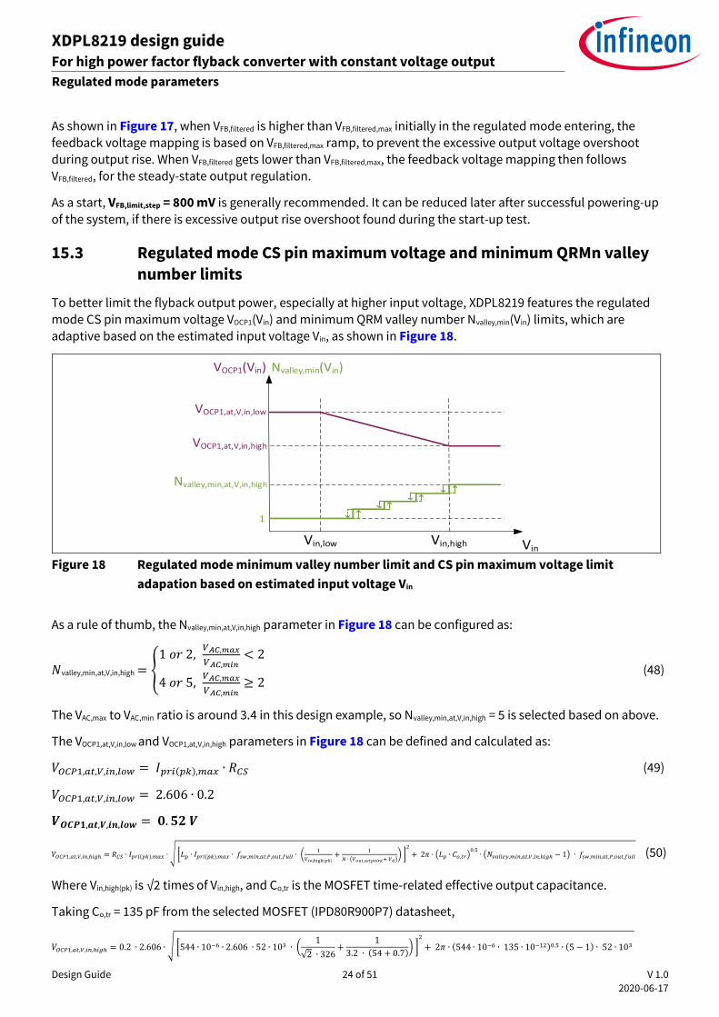
15.3 Regulated mode CS pin maximum voltage and minimum QRMn valley
number limits
To better limit the flyback output power, especially at higher input voltage, XDPL8219 features the regulated
mode CS pin maximum voltage VOCP1(Vin) and minimum QRM valley number Nvalley,min(Vin) limits, which are adaptive based on the estimated input voltage Vin, as shown in Figure 18.
VOCP1(Vin)
Vin,highVin,low Vin
VOCP1,at,V,in,low
VOCP1,at,V,in,high
Nvalley,min,at,V,in,high
1
Nvalley,min(Vin)
Figure 18 Regulated mode minimum valley number limit and CS pin maximum voltage limit
adapation based on estimated input voltage Vin
As a rule of thumb, the Nvalley,min,at,V,in,high parameter in Figure 18 can be configured as:
𝑁valley,min,at,V,in,high = 1 𝑜𝑟 2,
𝑉𝐴𝐶,𝑚𝑎𝑥
𝑉𝐴𝐶,𝑚𝑖𝑛< 2
4 𝑜𝑟 5,𝑉𝐴𝐶,𝑚𝑎𝑥
𝑉𝐴𝐶,𝑚𝑖𝑛≥ 2
(48)
The VAC,max to VAC,min ratio is around 3.4 in this design example, so Nvalley,min,at,V,in,high = 5 is selected based on above.
The VOCP1,at,V,in,low and VOCP1,at,V,in,high parameters in Figure 18 can be defined and calculated as:
𝑉𝑂𝐶𝑃1,𝑎𝑡,𝑉,𝑖𝑛,𝑙𝑜𝑤 = 𝐼𝑝𝑟𝑖(𝑝𝑘),𝑚𝑎𝑥 ∙ 𝑅𝐶𝑆 (49)
𝑉𝑂𝐶𝑃1,𝑎𝑡,𝑉,𝑖𝑛,𝑙𝑜𝑤 = 2.606 ∙ 0.2
𝑽𝑶𝑪𝑷𝟏,𝒂𝒕,𝑽,𝒊𝒏,𝒍𝒐𝒘 = 𝟎. 𝟓𝟐 𝑽
𝑉𝑂𝐶𝑃1,𝑎𝑡,𝑉,𝑖𝑛,ℎ𝑖𝑔ℎ = 𝑅𝐶𝑆 ∙ 𝐼𝑝𝑟𝑖(𝑝𝑘),𝑚𝑎𝑥 ∙ √ [𝐿𝑝 ∙ 𝐼𝑝𝑟𝑖(𝑝𝑘),𝑚𝑎𝑥 ∙ 𝑓𝑠𝑤,𝑚𝑖𝑛,𝑎𝑡,𝑃,𝑜𝑢𝑡,𝑓𝑢𝑙𝑙 ∙ (1
𝑉𝑖𝑛,high(𝑝𝑘)+
1
𝑁 ∙ (𝑉𝑜𝑢𝑡,𝑠𝑒𝑡𝑝𝑜𝑖𝑛𝑡+ 𝑉𝑑)) ]
2
+ 2𝜋 ∙ (𝐿𝑝 ∙ 𝐶𝑜,𝑡𝑟)0.5
∙ (𝑁𝑣𝑎𝑙𝑙𝑒𝑦,𝑚𝑖𝑛,𝑎𝑡,𝑉,𝑖𝑛,ℎ𝑖𝑔ℎ − 1) ∙ 𝑓𝑠𝑤,𝑚𝑖𝑛,𝑎𝑡,𝑃,𝑜𝑢𝑡,𝑓𝑢𝑙𝑙 (50)
Where Vin,high(pk) is √2 times of Vin,high, and Co,tr is the MOSFET time-related effective output capacitance.
Taking Co,tr = 135 pF from the selected MOSFET (IPD80R900P7) datasheet,
𝑉𝑂𝐶𝑃1,𝑎𝑡,𝑉,𝑖𝑛,ℎ𝑖𝑔ℎ = 0.2 ∙ 2.606 ∙ √ [544 ∙ 10−6 ∙ 2.606 ∙ 52 ∙ 103 ∙ (1
√2 ∙ 326+
1
3.2 ∙ (54 + 0.7)) ]
2
+ 2𝜋 ∙ (544 ∙ 10−6 ∙ 135 ∙ 10−12)0.5 ∙ (5 − 1) ∙ 52 ∙ 103

Design Guide 25 of 51 V 1.0
2020-06-17
XDPL8219 design guide For high power factor flyback converter with constant voltage output
Regulated mode parameters
𝑽𝑶𝑪𝑷𝟏,𝒂𝒕,𝑽,𝒊𝒏,𝒉𝒊𝒈𝒉 = 𝟎. 𝟒𝟑 𝑽
Note: VOCP1,at,V,in,high parameter is configurable between 0.34 V and VOCP1,at,Vin,low level only. If the calculated VOCP1,at,V,in,high is below 0.34 V, VOCP1,at,Vin,high = 0.34 V should be selected. If the calculated VOCP1,at,V,in,high is
above the configured VOCP1,at,Vin,low, then VOCP1,at,Vin,high should be configured as per VOCP1,at,Vin,low.
15.4 On-time limits
The maximum and minimum on-time limits in Figure 19 are adaptive based on the estimated input voltage Vin.
• QRMn/DCM:
To sense the output overvoltage level of VoutOV parameter, the device calculates a ton,min,V,out,sense(Vin) variable, which is the estimated minimum on-time to achieve the desired minimum transformer demagnetization time of tmin,demag parameter, at the peak of the estimated input voltage Vin,peak. The minimum on-time limit ton,min(Vin)
is based on the ton,min parameter or the ton,min,V,out,sense(Vin) variable, whichever is higher, as shown in Figure 19.
For Vin between the lowest operational input voltage parameter Vin,low and the input overvoltage protection
level parameter VinOV, the maximum on-time limit ton,max(Vin) is scaled to compensate the influence of input voltage on feedback gain.
For Vin from Vin,low to the input undervoltage protection level parameter Vin,UV, ton,max(Vin) can be linearly reduced from ton,max,at,V,in,low parameter to ton,max,at, Vin,UV parameter, to limit the maximum power during brown-out.
• ABM:
For Vin decreased from Vin,high, the ABM minimum on-time limit ton,min,ABM(Vin) is increased from ton,min,ABM
parameter, to reduce the burst pulse number for a lower standby power at lower input voltage.
Vin,lowVinUV VinOV
ton,max,at,V,in,low
ton,min
ton,max(Vin)ton,min,V,out,sense(Vin)
ton,min(Vin)
Note:ton,max,at,V,in,low – [(ton,max,at,V,in,low - ton,max,at,V,in,UV) · Vin / (Vin,low - VinUV)] when Vin < Vin,low
ton,min,V,out,sense(Vin) = tmin,demag · (Np / Ns) · (VoutOV / Vin,peak)`
ton,max,at,V,in,low · (Vin,low / Vin) when Vin Vin,low and Nvalley = 1
Vin
ton,min,ABM(Vin)
ton,max,at,V,in,UV
Vin,high
ton,min,ABM
ton,min,ABM · (Vin,high / Vin) when Vin < Vin,high
ton,min,ABM when Vin Vin,high
ton,min,ABM(Vin) =
Nvalley =1
Nvalley = Nvalley,min,at,V,in,high
ton,max(Vin) =
(E.g. Using 4 as example)
Figure 19 On-time limit adaptation based on estimated input voltage Vin

Design Guide 26 of 51 V 1.0
2020-06-17
XDPL8219 design guide For high power factor flyback converter with constant voltage output
Regulated mode parameters
The recommended on-time limits related parameter configuration from Table 6 is selected in this design
example.
Table 6 On-time limits parameter configuration
Parameter name Recommended value Unit
ton,max,at,V,in,low Refer to calculation in Section 13 µs
ton,max,at,V,in,UV Refer to calculation in Section 13 µs
tmin,demag 2 µs
ton,min 1.38 µs
ton,min,ABM 1 µs
15.5 ABM FB voltage sensing and control
In ABM, the switching pulse on-time ton and burst pulse number NABM are controlled based on VFB,filtered taken at the last pulse of the previous burst cycle, as shown in Figure 20. The ABM minimum on-time and minimum
pulse number per burst are based on the ton,min,ABM(Vin) and nABM,min parameters, respectively.
During ABM burst pause, the controller enters sleep mode with the FB pin internal pull-up disabled, to reduce
the power consumption. Before the next ABM burst pulse starts, the controller wakes up with the FB pin internal pull-up re-enabled. To avoid measuring the FB pin voltage spikes, which could present initially when
the internal pull-up is re-enabled, the start of both ABM burst pulsing and FB pin voltage sampling is delayed upon the controller wake-up, based on the nwakeup parameter.
Typically, the controller has a burst interval which is approximately the configured 1/fburst and enters the sleep
mode for power saving after completing the last pulse of each burst cycle, as shown in Figure 20.
However, if the UART reporting feature is enabled with ENUART,reporting parameter, either a longer than typical burst interval or a delayed sleep mode entry, or both can occur occasionally, for instance when the UART signal
transmission can not be completed within the typical burst interval or before the last pulse of a burst cycle.
VGD
VFB
nwakeup
T 1/fburstT 1/fburst
nABM = 4
VFB,filtered
nwakeup nwakeup
x 19 µsx 19 µs x 19 µs
nABM = 4
ton = α
Approx.Approx. Approx.
1/fsw,min 1/fsw,min 1/fsw,min
ton = α
nABM = 3ton = β
nABM = 3ton = β
t
t
wakeup
sleepwake
upsleepsleep
wakeup
ton = β nABM = 3
Figure 20 Typical ABM switching waveforms
Referring to Table 7, the recommended parameter configuration for ABM FB voltage sensing and control is selected in this design example.

Design Guide 27 of 51 V 1.0
2020-06-17
XDPL8219 design guide For high power factor flyback converter with constant voltage output
Regulated mode parameters
Table 7 Parameter configuration related to ABM FB voltage sensing and control
Parameter name Recommended value Unit
fburst 130 Hz
nABM,min 3 –
ton,min,ABM 1.00 µs
nwakeup 3 Interval (each interval is around 19 µs)
15.6 Filtered FB voltage mapping and mode transition
ABM QRMn DCM
tsw,min
VFB,filtered
VFB,swVFB,on
ton,min(Vin)
ton,max(Vin)
1/fsw,min
1/fsw,max
VFB,ABM
VFB,max,map
VFB,min
nABM,min
nABM ton
ton,min,ABM(Vin)
VREF(2.428V typ.)
(0.8V typ.)
(26.9 kHz typ.)
tsw,QRMn ton
nABM,max fsw,min/fburst(26.9kHz typ.)
NValley
Nvalley,max
1
VFB,valley,1
VFB,valley,max
(0.8V typ.)
(0.8V typ.)
tsw,min
, when Nvalley,min(Vin) = 1
E.g. 9 as example
Figure 21 Filtered FB voltage mapping
• QRMn/DCM:
The ton, tsw,min and Nvalley in Figure 21 are mapped from the filtered feedback voltage VFB,filtered.
In QRMn, to switch on the MOSFET at the Nvalley of the drain voltage, the system-dependent QRMn switching period tsw,QRMn has to be more than tsw,min. If the drain voltage valley of Nvalley happens before tsw,min is reached, the controller operates in DCM and the DCM switching period tsw,DCM follows tsw,min.
The minimum switching period tsw,min is decreased from 1/fsw,min (37.2 µs typ.) to 1/fsw,max when VFB,filtered is
increased from VFB,ABM parameter (0.8 V typ.) to VFB,sw parameter or more. fsw,min and fsw,max are respectively the minimum and maximum switching frequency parameters.
When VFB,filtered is VFB,valley,max parameter, Nvalley is mapped to the maximum valley number parameter Nvalley,max. The minimum Nvalley value is however based on Nvalley,min(Vin), as described in Section 15.3 . When Nvalley,min(Vin) is 1 and the VFB,filtered is the same as or higher than VFB,valley,1 parameter,Nvalley is mapped to 1.

Design Guide 28 of 51 V 1.0
2020-06-17
XDPL8219 design guide For high power factor flyback converter with constant voltage output
Regulated mode parameters
For a smoother transition when the Nvalley changes, the device can compensate the ton curve using cvalley,comp parameter. To stabilize the Nvalley in steady state operation, a hysteresis on Nvalley change is applied, and the Nvalley is only updated once in each operation cycle. If the Nvalley change is more than a Nvalley,fast parameter, the controller can speed up the Nvalley update for a better dynamic load response.
When VFB,filtered increases from VFB,on parameter (0.8 V typ.), ton increases from ton,min(Vin). When VFB,filtered Is
increased to VFB,max,map parameter or more, the power transfer is maximum, with the ton based on ton,max(Vin) or VOCP1(Vin), and the switching period depending on either 1/fsw,max or the minimum QRMn valley number limit Nvalley,min(Vin).
• ABM:
ton and nburst are mapped from VFB,filtered taken at the last pulse of previous burst cycle.
VFB,ABM parameter (0.8 V typ.) is the VFB,filtered threshold for ABM entry and exit. To enter ABM, VFB,filtered needs to be below the VFB,ABM threshold, for a minimum time-out based on the tABM,blank parameter. If ENBurst,Exit,Filter,Feedback parameter is enabled, ABM will be exited when VFB,filtered rises above the VFB,ABM threshold. If it is disabled, ABM will be exited when the sampled FB voltage rises above the VFB,ABM threshold.
When VFB,filtered decreases from VFB,ABM parameter (0.8 V typ.) to VFB,min parameter, ton decreases from ton,min(Vin) to ton,min,ABM(Vin), while nburst decreases from nABM,max to nABM,min parameter. nABM,max is an integer which is
approximately the ratio of fsw,min parameter over fburst parameter.
When VFB,filtered is the same as or lower than the VFB,min parameter, the power transfer is minimum, with the ton based on ton,min,ABM(Vin) and pulse number nABM based on nABM,min.
Referring to Table 8, the recommended parameter configuration for FB voltage mapping and mode transition
is selected in this design example.
Table 8 Parameter configuration related to FB voltage mapping and mode transition
Parameter name Recommended value Unit
fsw,max 186.4 kHz
ENBurst,Exit,Filter,Feedback Enabled
tABM,blank 6.5 ms
Nvalley,max 14
Nvalley,fast 9
Cvalley,comp 3.0
VFB,valley,1 1.5 V
VFB,max,map 2.0 V
VFB,sw 1.5 V
VFB,min VCE(sat) (refer to optocoupler datasheet,
as described in Section 14)
V
Design Guide 29 of 51 V 1.0
2020-06-17
XDPL8219 design guide For high power factor flyback converter with constant voltage output
UART reporting
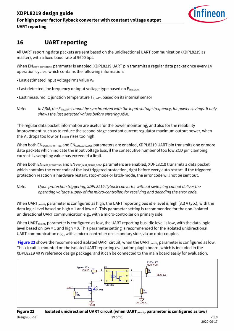
16 UART reporting
All UART reporting data packets are sent based on the unidirectional UART communication (XDPL8219 as
master), with a fixed baud rate of 9600 bps.
When ENUART,REPORTING parameter is enabled, XDPL8219 UART pin transmits a regular data packet once every 14 operation cycles, which contains the following information:
• Last estimated input voltage rms value Vin
• Last detected line frequency or input voltage type based on Fline,UART
• Last measured IC junction temperature TJ,UART, based on its internal sensor
Note: In ABM, the Fline,UART cannot be synchronized with the input voltage frequency, for power savings. It only shows the last detected values before entering ABM.
The regular data packet information are useful for the power monitoring, and also for the reliability
improvement, such as to reduce the second-stage constant current regulator maximum output power, when the Vin drops too low or TJ,UART rises too high.
When both ENUART,REPORTING and ENSEND,V,IN,LOSS parameters are enabled, XDPL8219 UART pin transmits one or more
data packets which indicate the input voltage loss, if the consecutive number of too low ZCD pin clamping current -IIV sampling value has exceeded a limit.
When both ENUART,REPORTING and ENSEND,LAST,ERROR,CODE parameters are enabled, XDPL8219 transmits a data packet
which contains the error code of the last triggered protection, right before every auto restart. If the triggered
protection reaction is hardware restart, stop-mode or latch-mode, the error code will not be sent out.
Note: Upon protection triggering, XDPL8219 flyback converter without switching cannot deliver the operating voltage supply of the micro-controller, for receiving and decoding the error code.
When UARTpolarity parameter is configured as high, the UART reporting bus idle level is high (3.3 V typ.), with the
data logic level based on high = 1 and low = 0. This parameter setting is recommended for the non-isolated unidirectional UART communication e.g., with a micro-controller on primary side.
When UARTpolarity parameter is configured as low, the UART reporting bus idle level is low, with the data logic level based on low = 1 and high = 0. This parameter setting is recommended for the isolated unidirectional UART communication e.g., with a micro-controller on secondary side, via an opto-coupler.
Figure 22 shows the recommended isolated UART circuit, when the UARTpolarity parameter is configured as low. This circuit is mounted on the isolated UART reporting evaluation plugin board, which is included in the
XDPL8219 40 W reference design package, and it can be connected to the main board easily for evaluation.
Figure 22 Isolated unidirectional UART circuit (when UARTpolarity parameter is configured as low)

Design Guide 30 of 51 V 1.0
2020-06-17
XDPL8219 design guide For high power factor flyback converter with constant voltage output
UART reporting
Note: In Figure 22, VCC_P net connects to the positive polarity of either CVCC (if error code sending is needed), or Cout,aux, while the UART net connects to XDPL8219 UART pin, and PGND symbol connects to the primary ground.
The UART reporting data packet decoding and interpretation are shown in Table 9, Table 10 and Table 11.
Table 9 UART reporting data packet format for decoding
Type of data packet Byte 1 Byte 2 Byte 3 Byte 4 Byte 5 Byte 6
Regular data packet 7EH Low byte of
Vin,aux data
High byte of
Vin,aux data tin data T40 data
Checksum
(XOR sum of
Byte 1 to 5
before)
Typical loss of input voltage indication
data packet
40H - - - - -
Loss of input voltage indication within the
regular data packet
7EH
EDH
or
Low byte of
Vin,aux data
EDH
or
High byte of
Vin,aux data
EDH
or
tin data
EDH
or
T40 data
EDH
Error code data
packet 60H
Low byte of
Error code
High byte of
Error code
Checksum
(XOR sum of
Byte 1 to 3
before)
- -
Table 10 Interpretation of the decoded regular data
Regular data
type
Decoded regular
data minimum
decimal value
Decoded regular
data maximum
decimal value
Data interpretation
tin 0 255
If tin = FFH, the input voltage type has not been detected.
If tin = 00H, the last detected input voltage type is constant DC.
If tin ≠ FFH and tin ≠ 00H, the last detected input voltage type is
AC and the Fline,UART (unit: Hz) can be calculated based on:
𝐹𝑙𝑖𝑛𝑒,𝑈𝐴𝑅𝑇 = 5828 𝑡𝑖𝑛⁄ , 𝑇𝑐𝑟𝑖𝑡𝑖𝑐𝑎𝑙 > 119°𝐶
7726 𝑡𝑖𝑛⁄ , 𝑇𝑐𝑟𝑖𝑡𝑖𝑐𝑎𝑙 ≤ 119°𝐶
Where Tcritical is the IC overtemperature protection level
parameter setting.
Vin,aux 0 40960 𝑽𝒊𝒏
= 𝟎. 𝟎𝟎𝟓𝟒𝟔𝟎 ∙ 𝑽𝒊𝒏,𝒂𝒖𝒙 ∙ 𝑵𝒑 𝑵𝒂⁄ , 𝒕𝒊𝒏 ≠ 𝑭𝑭𝑯 𝒂𝒏𝒅 𝒕𝒊𝒏 ≠ 𝟎𝟎𝑯
𝟎. 𝟎𝟎𝟕𝟕𝟐𝟐 ∙ 𝑽𝒊𝒏,𝒂𝒖𝒙 ∙ 𝑵𝒑 𝑵𝒂⁄ , 𝒕𝒊𝒏 = 𝟎𝟎𝑯
T40 0 190 𝑻𝑱,𝑼𝑨𝑹𝑻 = 𝑻𝟒𝟎 − 𝟒𝟎
Note: The micro-controller receiving the regular data packet should do the averaging on the decoded Vin and Fline,UART data samples, to obtain the more stable value.

Design Guide 31 of 51 V 1.0
2020-06-17
XDPL8219 design guide For high power factor flyback converter with constant voltage output
UART reporting
Note: The microcontroller should store the necessary calibration data for its post-processing, to compensate the offset on Vin,, which varies based on the IC and system tolerances of each board.
Table 11 Interpretation of the error code data
Error code data Last triggered protection
UARTpolarity = High UARTpolarity= Low
0000H FFFFH None
0001H FFFEH Output OVP
0008H FFF7H Regulated mode output UVP
0010H FFEFH Start-up output UVP
0020H FFDFH Transformer demagnetization time shortage protection
0040H FFBFH Input UVP
0080H FF7F H Input OVP
0100H FEFFH IC overtemperature protection
0200H FDFFH VCC OVP
0400H FBFFH Interrupt watchdog protection (may get triggered for input UVP)
0800H F7FFH MOSFET over-current protection
4000H BFFFH ADC watchdog protection (may get triggered for input UVP)
8000H 7FFF H Regulated mode VCC UVP
In this design example, ENUART,REPORTING = Enabled, ENSEND,V,IN,LOSS = Enabled, ENSEND,LAST,ERROR,CODE = Enabled and
UARTpolarity = Low parameter settings are selected.
Design Guide 32 of 51 V 1.0
2020-06-17
XDPL8219 design guide For high power factor flyback converter with constant voltage output
Other functions and protections
17 Other functions and protections
17.1 Enhanced power factor correction
To compensate for the input current displacement caused by the CDC,filter and line filter, the XDPL8219 enhanced power factor correction (EPFC) feature can be enabled by configuring the correction gain parameter named CEMI
above zero. As a start, it can be configured as per the CDC,filter value. Therefore, the initial CEMI = 0.22 𝝁F parameter setting is selected in this design example.
The EFPC gain is reduced from CEMI parameter to zero for a smooth transition to ABM, when the VFB,filtered is decreased from VEPFC,on parameter to VFB,ABM parameter (0.8 V typ.). VEPFC,on = 1 V parameter setting is
recommended and selected in this design example.
Upon successful powering-up of the system, refer to Section 20.3 for the fine-tuning guide.
17.2 Enhanced THD correction
By enabling the ENETHDC parameter, the controller compensates the input current distortion caused by the
changing QRMn duty cycle over the AC input half-sine-wave period. Such compensation can however increases
the EMI at higher input voltage, caused by the higher switching peak current. Hence, it is only recommended to
enable the ENETHDC parameter when the extremely low THD is required at full output power, where the QRM valley number is the lowest and such compensation effect would be the highest.
Using the XDPL8219 40 W reference design as an example, even with ENETHDC parameter disabled by default, THD less than 10 percent can be achieved over wide operating range. In this design example, ENETHDC = Disabled
parameter setting is selected.
Upon successful powering-up of the system, refer to Section 20.3 for the fine-tuning guide.
17.3 Switching frequency dithering for constant DC input
To lower the EMI while operating with a constant DC input voltage, the switching frequency dithering feature can be enabled by configuring the cdither parameter above zero. Based on the modulation gain parameter cdither,
ton and tsw,min are modulated in QRMn and DCM, while tsw,min is modulated in ABM, to dither the switching frequency.
cdither = 10 percent parameter setting is recommended and selected in this design example.
17.4 Auto restart time
For all protections with the auto restart reaction, the auto restart time is common and configurable based on tauto,restart parameter.
tauto,restart = 1.2 sec parameter setting is recommended and selected in this design example.
17.5 VCC OVP
The VCC overvoltage protection (OVP) reaction is configurable to latch-mode or auto restart, based on the ReactionVCC,OVP parameter. In addition, the VCC OVP level is also configurable based on the VVCC,max parameter.
ReactionVCC,OVP = Latch-Mode and VVCC,max = 23 V are recommended and selected in this design example.

Design Guide 33 of 51 V 1.0
2020-06-17
XDPL8219 design guide For high power factor flyback converter with constant voltage output
Other functions and protections
17.6 Regulated mode VCC UVP
ENVCC,UVP parameter refers to the enable switch for the regulated mode VCC undervoltage protection (UVP). The
protection reaction is fixed as auto restart and it is triggered when VCC voltage is the same as or lower than regulated mode VCC UVP level of VVCC,min, for longer than a blanking time.
ENVCC,UVP = Enabled and VVCC,min = 7.5 V parameter settings are recommended and selected in this design
example.
17.7 IC overtemperature protection
The IC overtemperature protection level is based on the Tcritical parameter. If Tcritical is configured above 119°C,
the maximum switching frequency parameter fsw,max cannot be configured above 186.4 kHz. The protection reaction is fixed as auto restart, while the maximum junction temperature for start-up/restart is fixed as 4°C below Tcritical.
Tcritical = 119°C is recommended and selected in this design example.
17.8 Primary MOSFET over-current protection
VOCP2 denotes the CS pin voltage level 2 for the primary MOSFET over-current protection. Under the single-fault condition of shorted primary main winding, the primary MOSFET over-current protection is triggered when the
CS pin voltage exceeds VOCP2 for longer than a blanking time based on the tCSOCP2 parameter.
tCSOCP2 = 240 ns is recommended and selected in this design example.
VOCP2 level is automatically selected based on Table 12. In this design example, VOCP1,at,V,in,low = 0.52 V is selected,
so VOCP2 = 0.8 V is applied automatically. The protection reaction is fixed as auto restart.
Table 12 VOCP2 level selection based on VOCP1,at,V,in,low parameter value
VOCP1,at,V,in,low (V) VOCP2 (V)
0.34 to 0.36 0.6
0.37 to 0.54 0.8
0.55 to 0.72 1.2
0.73 to 1.08 1.6
17.9 Debug mode
When the DebugMode parameter is enabled, the controller enters the stop mode, after a protection is triggered except for the VCC undervoltage lockout. There is no GD pin switching in stop mode and the controller stays in
this mode to allow the error code readout for identifying the triggered protection, as long as the VCC stays above
the VUVOFF (6 V typ.).
The parameter setting of DebugMode = Disabled is selected in this design example. The DebugMode parameter should only be enabled for debugging purposes.

Design Guide 34 of 51 V 1.0
2020-06-17
XDPL8219 design guide For high power factor flyback converter with constant voltage output
PCB layout guide
18 PCB layout guide
a) Minimize the circumference of the following high-current/high-frequency loop with traces which are short
and wide (or with jumper wires which are short and thick).
Power switch loop formed by DC link filter capacitor CDC,filter , primary main winding , flyback MOSFET
and CS resistor RCS.
Main output rectifier loop formed by secondary main winding, main output diode and main output capacitor.
Auxiliary output rectifier loop formed by auxiliary winding, auxiliary output diode and auxiliary output capacitor.
b) Place each filter capacitor, VCC noise decoupling capacitor CVCCdecouple, ZCD pin filter capacitor CZCD and FB pin filter capacitor CFB near to its designated pin and the GND pin of the controller.
c) Apply the following guide for star grounding.
Connect ground signal traces of CVCCdecouple, CZCD, RZCD,2, CFB, the controller GND pin and the optocoupler
emitter pin.
Connect VCC ground traces of the VCC capacitor CVCC and primary auxiliary winding.
Connect the CHV GND pin near to the ground pin of CDC,filter.
Connect the GND pin of each CVCC, CVCCdecouple, RCS and bridge rectifier separately to a single point near
CDC,filter.
d) Ensure the high dv/dt traces from the MOSFET drain and GD pin are as far as possible from the FB pin and
its connected trace.
e) Shield signal traces with ground traces or ground plane, which can help to reduce noise pick-up.
f) Always ensure appropriate safety clearances between the high voltage and low voltage nets.

Design Guide 35 of 51 V 1.0
2020-06-17
XDPL8219 design guide For high power factor flyback converter with constant voltage output
Parameter configuration list, setup and procedures
19 Parameter configuration list, setup and procedures
19.1 Parameter configuration list
Figure 23 shows the XDPL8219 parameter configuration list, with selected values based on the design examples from Section 2 to Section 17. For another system design, the values in the list can be different.
For the IC parameter configuration setup and procedures, please refer to Section 19.2 and Section 19.3. For safety purposes, before powering up the board, it is important to ensure that the configured IC parameter values in the hardware configuration section in Figure 23 are compatible with the actual system hardware dimensioning.
Figure 23 IC parameter configuration list with selected values based on design examples from
Section 2 to Section 17
Note: UserID,A parameter in Figure 23 has no effect on the IC behavior and system performance. By default, the value of this parameter is set to zero. If necessary, it can be configured to store system
information, such as parameter version, LED driver model, etc.
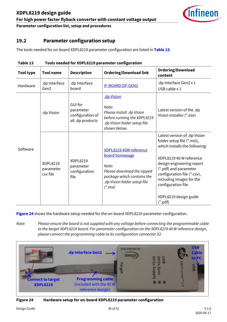
Design Guide 36 of 51 V 1.0
2020-06-17
XDPL8219 design guide For high power factor flyback converter with constant voltage output
Parameter configuration list, setup and procedures
19.2 Parameter configuration setup
The tools needed for on-board XDPL8219 parameter configuration are listed in Table 13.
Table 13 Tools needed for XDPL8219 parameter configuration
Tool type Tool name Description Ordering/Download link Ordering/Download
content
Hardware .dp Interface
Gen2
.dp Interface
board IF-BOARD.DP-GEN2
.dp Interface Gen2 x 1
USB cable x 1
Software
.dp Vision
GUI for parameter configuration of
all .dp products
.dp Vision
Note: Please install .dp Vision
before running the XDPL8219 .dp Vision folder setup file shown below.
Latest version of the .dp
Vision installer (*.exe)
XDPL8219
parameter
csv file
XDPL8219 parameter
configuration
file
XDPL8219 40W reference board homepage
Note:
Please download the zipped
package which contains the
.dp Vision folder setup file (*.msi)
Latest version of .dp Vision
folder setup file (*.msi),
which installs the following:
XDPL8219 40 W reference
design engineering report
(*.pdf) and parameter configuration file (*.csv), including images for the
configuration file.
XDPL8219 design guide
(*.pdf)
Figure 24 shows the hardware setup needed for the on-board XDPL8219 parameter configuration.
Note: Please ensure the board is not supplied with any voltage before connecting the programmable cable to the target XDPL8219 board. For parameter configuration on the XDPL8219 40 W reference design, please connect the programming cable to its configuration connector X2.
Figure 24 Hardware setup for on-board XDPL8219 parameter configuration
USB Cable
to PC
.dp Interface Gen2
Programming cable (included with the 40 W
reference design)
Connect to target
XDPL8219
Vcc UART GND

Design Guide 37 of 51 V 1.0
2020-06-17
XDPL8219 design guide For high power factor flyback converter with constant voltage output
Parameter configuration list, setup and procedures
19.3 Parameter configuration procedures
After the hardware connections for XDPL8219 configuration (see Figure 24) are done, please start the program by clicking the shortcut “.dp Vision” on the desktop.
Note: During the program start-up, if the system shows there is a newer version of .dp Vision, please follow the procedure and update accordingly. As the screenshots were taken based on .dp Vision version
2.0.9.4, it might look different for newer versions of .dp Vision.
A .dp Vision user manual is available by clicking [Help] >> [Help contents], to provide the detailed instructions on how to use this GUI for parameter configuration. Alternatively, the following simple guide is also available
for quick and easy reference.
Open the XDPL8219 parameter configuration file (*.csv) from the default installation folder at
C:\Users\<Username>\Infineon Technologies AG\.dp vision\Parameters, as shown in Figure 25.
Figure 25 Opening the XDPL8219 parameter configuration file (*.csv) in .dp Vision
After opening the parameter csv file, a list of configurable parameters with default values based on the reference board design will be shown (see the box on the left in Figure 26). These default values can be
changed for another board design, by referring to the design guide from Section 2 to Section 18 and the fine-tuning guide in Section 20.
If a parameter value is changed and no limit violation is found, the changed value itself will turn blue, like the example in Figure 26 which the Rcs parameter in the hardware configuration section has been changed from 0.2 Ω to 0.18 Ω. Otherwise, if an error is detected (e.g., exceeded min./max. value), the parameter value which caused the error will turn red and the message bar of .dp Vision (see the top right in Figure 26) will show an
error message. If any error is not resolved, the user is not allowed to configure the IC with the changed value.
Figure 26 Changing parameter values of XDPL8219 configuration file in .dp Vision
Note: For safety and proper system functioning, it is important to ensure the hardware configuration section
parameter values are compatible with the actual system hardware dimensioning.
Select XDPL8219
configuration file to open
List of configurable parameters Message Bar
Parameter value
change example
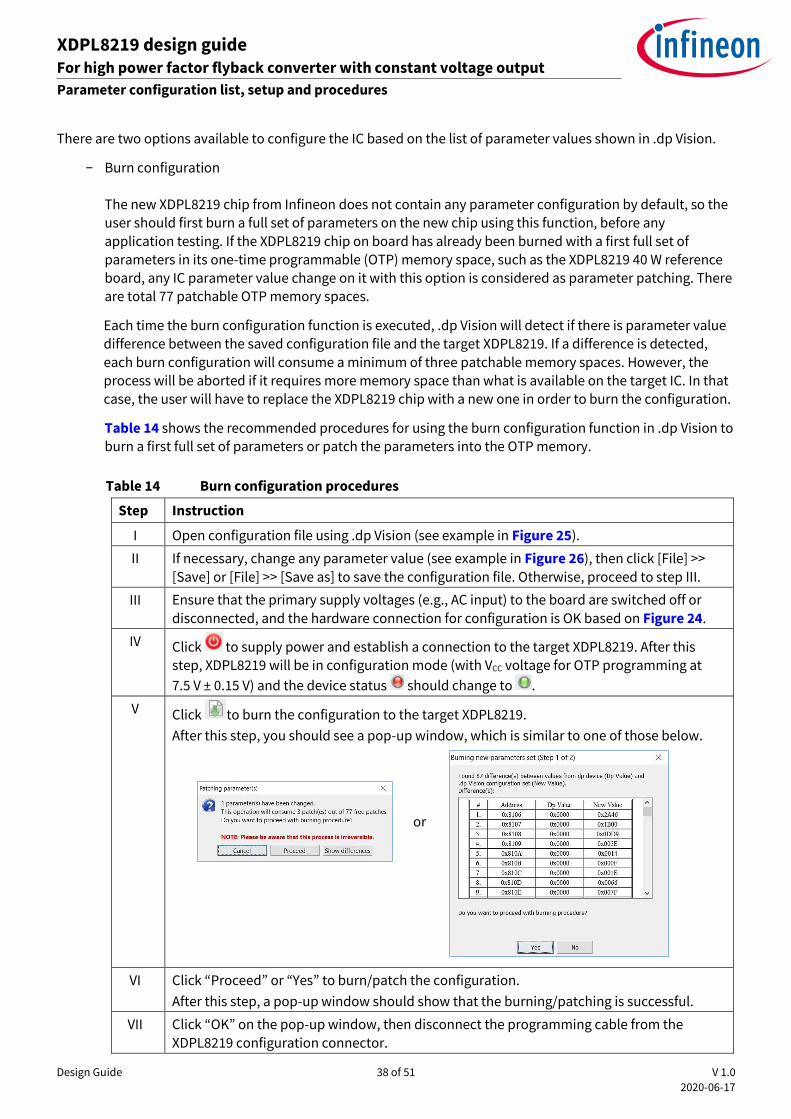
Design Guide 38 of 51 V 1.0
2020-06-17
XDPL8219 design guide For high power factor flyback converter with constant voltage output
Parameter configuration list, setup and procedures
There are two options available to configure the IC based on the list of parameter values shown in .dp Vision.
− Burn configuration
The new XDPL8219 chip from Infineon does not contain any parameter configuration by default, so the user should first burn a full set of parameters on the new chip using this function, before any
application testing. If the XDPL8219 chip on board has already been burned with a first full set of parameters in its one-time programmable (OTP) memory space, such as the XDPL8219 40 W reference board, any IC parameter value change on it with this option is considered as parameter patching. There
are total 77 patchable OTP memory spaces.
Each time the burn configuration function is executed, .dp Vision will detect if there is parameter value
difference between the saved configuration file and the target XDPL8219. If a difference is detected,
each burn configuration will consume a minimum of three patchable memory spaces. However, the process will be aborted if it requires more memory space than what is available on the target IC. In that
case, the user will have to replace the XDPL8219 chip with a new one in order to burn the configuration.
Table 14 shows the recommended procedures for using the burn configuration function in .dp Vision to
burn a first full set of parameters or patch the parameters into the OTP memory.
Table 14 Burn configuration procedures
Step Instruction
I Open configuration file using .dp Vision (see example in Figure 25).
II If necessary, change any parameter value (see example in Figure 26), then click [File] >>
[Save] or [File] >> [Save as] to save the configuration file. Otherwise, proceed to step III.
III Ensure that the primary supply voltages (e.g., AC input) to the board are switched off or
disconnected, and the hardware connection for configuration is OK based on Figure 24.
IV Click to supply power and establish a connection to the target XDPL8219. After this
step, XDPL8219 will be in configuration mode (with VCC voltage for OTP programming at
7.5 V ± 0.15 V) and the device status should change to .
V Click to burn the configuration to the target XDPL8219.
After this step, you should see a pop-up window, which is similar to one of those below.
VI Click “Proceed” or “Yes” to burn/patch the configuration.
After this step, a pop-up window should show that the burning/patching is successful.
VII Click “OK” on the pop-up window, then disconnect the programming cable from the
XDPL8219 configuration connector.
or

Design Guide 39 of 51 V 1.0
2020-06-17
XDPL8219 design guide For high power factor flyback converter with constant voltage output
Parameter configuration list, setup and procedures
− Test configuration This function will download the parameter values from the list in .dp Vision into the XDPL8219 RAM, followed by an automatic IC start-up, for application testing with the new configuration (See the
recommended procedures in Table 15).
Unlike using the burn configuration, parameter configuration with this option is not permanent because the loaded RAM contents will be lost once the IC supply voltage is turned off, but the advantage of using this option is that it does not consume OTP memory space, thus there is no limit on
the number of parameter value changes.
Table 15 Test configuration procedures
Step Instruction
I Open the configuration file using .dp Vision (see example in Figure 25).
II Ensure that the primary supply voltages (e.g., AC input) to the board are switched off and the hardware connection for configuration is OK based on Figure 24, plus a low-ESR
ceramic capacitor of 1 nF soldered across the UART pin and ground for noise decoupling.
III Ensure ENUART,REPORTING parameter is disabled and change the desired parameter value (see
example in Figure 26).
Note: If the ENUART,REPORTING parameter is enabled, the success of test configuration cannot be guaranteed, since .dp Vision will show an error due to unable to get the status from XDPL8219
with UART reporting, after the automatic IC start-up with the new configuration in RAM.
IV Click to supply power and establish a connection to the target XDPL8219. After this step,
XDPL8219 will be in configuration mode and the device status should change to .
V Ensure the board test setup (e.g., output load) is OK, then apply the AC input to the board.
After this step, the board does not start-up because XDPL8219 is still in configuration mode.
VI Click to test the new configuration with the target XDPL8219.
VII If the IC automatically starts up with the new configuration, you should see a pop-up
window like the one shown below. Click “OK” to proceed.
Note: If there is any protection being triggered after step VI, the pop-up window would show
that the test configuration is unsuccessful; Please refer Section 21 for the debugging guide.
VIII To test another configuration change, repeat steps II to VII. If the following message box
appears in between the steps, click “Yes” to proceed.
Otherwise, turn-off the AC input and disconnect the programming cable from the XDPL8219
configuration connector.
Note: If any error occurs during the parameter configuration procedures, please refer to the message bar of
.dp Vision for the error description. For more details, please refer to the .dp Vision user manual.

Design Guide 40 of 51 V 1.0
2020-06-17
XDPL8219 design guide For high power factor flyback converter with constant voltage output
Fine-tuning guide
20 Fine-tuning guide
This section presents guidelines for how to fine-tune the value of a few essential XDPL8219 parameters, based
on the actual measurement waveform or data.
20.1 Input voltage-sensing parameter fine-tuning
When the primary MOSFET is switched on, the XDPL8219 measures the current flowing out of the ZCD pin -IIV, to estimate the DC link filter capacitor voltage VDC,filter.
Ideally, VDC,filter should be a low-frequency (e.g., typically 100 Hz ~ 120 Hz) rectified sinusoidal waveform, as shown in Figure 27, where the peak value of VDC,filter is equal to AC input peak value Vin,peak, and the estimated
input voltage Vin in rms value is assumed to be 0.707 times Vin,peak. However, due to the input line filter
impedance and the filter capacitor ESR, the actual VDC,filter has high switching frequency ripple (in the kHz range) over the low-frequency sinusoidal waveform, whose ripple peak-to-peak voltage level varies based on the peak current being drawn by the transformer primary main winding. Step III of Table 16 shows an example of the actual VDC,filter waveform.
To improve the input voltage estimation accuracy, Rin parameter fine-tuning is important for the IC to estimate the correct Vin,peak by compensating such switching frequency ripples, which appears in -IIV measurements as
well.
Na Np VDC,filter
ZCD
VAUX
IIV
VINPCLN
RZCD,1
RZCD,2 GD
CDC,filterVDC,filter
Vin,peak
RCS
RG
VCS
Vin
CZCD
Figure 27 –IIV measurement for input voltage sensing
Table 16 shows the recommended procedures for Rin parameter fine-tuning.
Table 16 Recommended procedures for Rin parameter fine-tuning
Step Instruction
I Apply two voltage probes on the board, which respectively measure the waveform of the DC link
filter capacitor voltage VDC,filter and CS pin voltage VCS.
II Ensure the target XDPL8219 has already been burned with at least a first full set of parameters.
Power up the board with normal operational minimum AC input voltage VAC,min and full load output.
If it cannot be powered up, retry by burning the input UVP to enable switch parameter ENUVP,In as
“Disabled” (if it was not before) or refer Section 21 for the debugging guide.
III Capture the voltage waveform with a time base of 1 ms and zoom into the peak voltage for measuring the minimum level of the VDC,filter high-frequency voltage ripple (VDC,HF,RIPPLE,MIN) and the
maximum level of VCS (VCS,max). Below is an example of a waveform captured on the 40 W reference
design with VAC,min = 90 Vrms, Fline = 60 Hz and full-load output (Iout = 0.8 A).

Design Guide 41 of 51 V 1.0
2020-06-17
XDPL8219 design guide For high power factor flyback converter with constant voltage output
Fine-tuning guide
IV Turn-off the AC input. Calculate R1 with the equation below and voltage measurements from step
III:
𝑅1 = 𝑅𝐶𝑆 ∙ ( √2 ∙ 𝑉𝐴𝐶,𝑚𝑖𝑛 − 𝑉𝐷𝐶,𝐻𝐹,𝑅𝐼𝑃𝑃𝐿𝐸,𝑀𝐼𝑁
𝑉𝐶𝑆,𝑚𝑎𝑥), based on full load output
Calculation example based on 40 W reference design with VAC,min = 90 Vrms, Fline = 60 Hz and full-load
output (Iout = 0.8 A):
𝑅1 = 0.2 ∙ (√2 ∙ 90 − 100.4
0.501) = 10.73 Ω
V Repeat step III to obtain another measurement of VDC,HF,RIPPLE,MIN and VCS,max based on 33 percent load.
VI Turn-off the AC input. Calculate R2 with the equation below and voltage measurements from
step V:
𝑅2 = 𝑅𝐶𝑆 ∙ ( √2 ∙ 𝑉𝐴𝐶,𝑚𝑖𝑛 − 𝑉𝐷𝐶,𝐻𝐹,𝑅𝐼𝑃𝑃𝐿𝐸,𝑀𝐼𝑁
𝑉𝐶𝑆,𝑚𝑎𝑥), based on 33 percent load output
Calculation example based on 40 W reference design with VAC,min = 90 Vrms, Fline = 60 Hz and 33
percent load output (Iout = 0.265 A):
𝑅2 = 0.2 ∙ ( √2 ∙ 90 − 116.6
0.281) = 7.59 Ω
VII Calculate the fine-tuned Rin parameter value with the following equation:
𝐹𝑖𝑛𝑒 𝑡𝑢𝑛𝑒𝑑 𝑅𝑖𝑛 = 0.5 ∙ (𝑅1 + 𝑅2) + 𝑅𝑑𝑠(𝑜𝑛),25 + 𝑅𝑑𝑐,𝑝𝑟𝑖,𝑤𝑖𝑛𝑑𝑖𝑛𝑔 + 𝑅𝐶𝑆
Where Rds(on),25°C is the MOSFET drain-source on-resistance at 25°C, and Rdc,pri,winding is the primary
main winding DC resistance.
Calculation example based on 40 W reference design:
𝐹𝑖𝑛𝑒 𝑡𝑢𝑛𝑒𝑑 𝑅𝑖𝑛 = 0.5 ∙ (10.73 + 7.59) + 0.9 + 0.265 + 0.2
𝑭𝒊𝒏𝒆 𝒕𝒖𝒏𝒆𝒅 𝑹𝒊𝒏 ≈ 𝟏𝟎. 𝟓 Ω
VIII Use the burn configuration in .dp Vision to patch the Rin parameter with the value from step VII and also enable the ENUVP,In parameter (if it was set to “Disabled” before). Then, verify the AC input UVP
accuracy at full load and low load.
20.2 QR valley switching parameter fine-tuning
Unlike conventional analog solutions which achieve QR valley switching by introducing an external hardware delay on the zero-crossing signal with the ZCD pin capacitor, the XDPL8219 ZCD pin capacitor is mainly used for noise filtering only. Therefore, a fixed capacitor value, e.g., 47 pF, can be used across designs of different power classes. To achieve QRMn, the XDPL8219 dynamically measures the resonant period and delays the MOSFET switch-on by a quarter of the resonant period after zero-crossing of the primary auxiliary winding voltage.
VDC,HF,RIPPLE,MIN = 100.4 V
VCS,max = 0.501 V
VDC,filter
VCS
Zoom in at the peak

Design Guide 42 of 51 V 1.0
2020-06-17
XDPL8219 design guide For high power factor flyback converter with constant voltage output
Fine-tuning guide
tZCDPD parameter fine-tuning is, however, necessary to compensate for XDPL8219 internal propagation delay in ZCD and also external delay caused by the noise-filtering capacitor at the ZCD pin. Table 17 shows the recommended procedures for tZCDPD parameter fine-tuning.
Table 17 Recommended procedures for tZCDPD parameter fine-tuning
Step Instruction
I Apply a differential probe on the board to measure the flyback MOSFET drain voltage waveform.
II Set the tZCDPD parameter to 0 and use the test configuration function in .dp Vision to power up the
board with lowest typical AC input voltage, e.g., 120 Vrms, and full-load output.
If the board cannot be powered up, please refer to Section 21 for the debugging guide.
III Capture the waveform with a 1 ms time base and zoom into the voltage peak with a 1 µs time base.
IV Place a horizontal cursor at the highest possible level which crosses two points on the resonance part of the waveform (see a and b below), and measure the time between them (ta-b). In the example below, which is based on the 40 W reference design, ta-b is measured to be approximately
744 ns.
V Set the tZCDPD parameter as approximately half of ta-b and burn the configuration with .dp Vision.
VI Disconnect the programming cable after burning, then power up the board and the flyback MOSFET drain voltage waveform should be switching at the QRM1 (see example below based on
the 40 W reference design with fine-tuned tZCDPD = 370 ns).
a b
ta-b
Zoom in at the peak
Zoom in at the peak
VDRAIN
VDRAIN
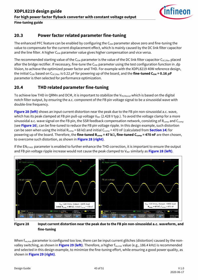
Design Guide 43 of 51 V 1.0
2020-06-17
XDPL8219 design guide For high power factor flyback converter with constant voltage output
Fine-tuning guide
20.3 Power factor related parameter fine-tuning
The enhanced PFC feature can be enabled by configuring the CEMI parameter above zero and fine-tuning the value to compensate for the current displacement effect, which is mainly caused by the DC link filter capacitor
and the line filter. A higher CEMI parameter value gives higher compensation and vice versa.
The recommended starting value of the CEMI parameter is the value of the DC link filter capacitor CDC,filter placed
after the bridge rectifier. If necessary, fine-tune the CEMI parameter using the test configuration function in .dp Vision, to achieve the optimized power factor and THD. For example with the XDPL8219 40W reference design, the initial CEMI based on CDC,filter is 0.22 𝜇F for powering up of the board, and the fine-tuned CEMI = 0.16 𝝁F
parameter is then selected for performance optimization.
20.4 THD related parameter fine-tuning
To achieve low THD in QRMn and DCM, it is important to stabilize the VFB,filtered which is based on the digital
notch filter output, by ensuring the a.c. component of the FB pin voltage signal to be a sinusoidal wave with double-line frequency.
Figure 28 (left) shows an input current distortion near the peak due to the FB pin non-sinusoidal a.c. wave, which has its peak clamped at FB pin pull-up voltage VREF (2.428 V typ.). To avoid the voltage clamp for a more
sinusoidal a.c. wave signal on the FB pin, the SSR feedback compensation network, consisting of Rcomp and Ccomp (see Figure 16), can be fine-tuned to reduce the FB pin voltage ripple. In this design example, such distortion can be seen when using the initial Rcomp = 68 kΩ and initial Ccomp = 470 nF (calculated from Section 14) for
powering up of the board. Therefore, the fine-tuned Rcomp = 47 kΩ, fine-tuned Ccomp = 470 nF are then chosen,
to overcome such distortion, as shown in Figure 28 (right).
If the ENETHDC parameter is enabled to further enhance the THD correction, it is important to ensure the output
and FB pin voltage ripple increase would not cause the peak clamped to VREF similarly as Figure 28 (left).
Figure 28 Input current distortion near the peak due to the FB pin non-sinusoidal a.c. waveform, and
fine-tuning
When fsw,max parameter is configured too low, there can be input current glitches (distortion) caused by the non-
valley switching, as shown in Figure 29 (left). Therefore, a higher fsw,max value (e.g., 186.4 kHz) is recommended and selected in this design example, to minimize the fine-tuning effort, while ensuring a good power quality, as shown in Figure 29 (right).

Design Guide 44 of 51 V 1.0
2020-06-17
XDPL8219 design guide For high power factor flyback converter with constant voltage output
Fine-tuning guide
Figure 29 Input current glitches (distortion), when fsw,max is too low
When Nvalley,min,at,V,in,high parameter is configured too low for an universal input design, there can be input current glitches (distortion) at higher input voltage, which are caused by the non-valley switching and changing quasi-
resonant duty cycle over the half-sine wave period, as shown in Figure 30 (left). Therefore, a higher Nvalley,min,at,V,in,high value (e.g., 4 or 5) is recommended for an universal input design and selected in this design
example, to minimize the fine-tuning effort, while ensuring a good power quality, as shown in Figure 30 (right).
Figure 30 Input current glitches (distortion) at higher input voltage, when Nvalley,min,at,V,in,high is too low
for an universal input design

Design Guide 45 of 51 V 1.0
2020-06-17
XDPL8219 design guide For high power factor flyback converter with constant voltage output
Debugging guide
21 Debugging guide
This section presents the guidelines for system debugging, if the board has any problem with powering up or
shutting down during testing.
With XDPL8219, there are 3 debugging options, to identify the triggered protection for the powering up or shutting down problem:
i) UART reporting error code readout (Refer the procedures in Section 21.1)
ii) Debug mode error code readout by test configuration (Refer the procedures in Section 21.2)
iii) Debug mode error code readout by burn configuration (Refer the procedures in Section21.3)
Figure 31 presents the flowchart to systematically choose the suitable debugging option for the problem, depending on the following checkpoints:
- Does VCC drop to VUVOFF (6 V typ.) when the powering up or shutting down problem takes place? (Yes/No)
- Is the UART reporting feature enabled for the target application? (Yes/No)
- Is there any ABM operation, ABM entering or exiting, needed to trigger the powering up or shutting down problem? (Yes/No/Not sure)
Start
ENUART,REPORTING
= Enabled?
UART reporting
error code readout
VCC dropped
to VUVOFF
(6 V typ.)?
Yes Yes
Debug mode
Error code readout by
Burn configuration
Any ABM
operation, ABM
entering or exiting
before protection
triggered?
No
Debug mode
Error code readout by
Test configuration No / Not sure
Error code
Readout
success?
A
A
End
Yes
Error code
Readout
success?
No
Yes
No
Yes
Error code
Readout
success?
Yes
The powering up
or shutting down
problem was due
to VCC under-
voltage lockout
triggering.
Please check the
VCC self supply.
No
No
Figure 31 Flowchart to choose the debugging option (for powering up or shutting down problem)
Depending the error code readout success of the first debugging option recommended by the flowchart, a
second debugging option might be recommended by the flowchart, to read out the error code or to identify the triggered protection.
(Refer Section 21.1)
(Refer Section 21.2)
(Refer Section 21.3)

Design Guide 46 of 51 V 1.0
2020-06-17
XDPL8219 design guide For high power factor flyback converter with constant voltage output
Debugging guide
21.1 UART reporting error code readout
Table 18 Procedures for UART reporting error code readout
Step Instruction
I Open the configuration file (see the example in Figure 25) used in the system which has the
powering up or shutting down problem.
II If both UARTREPORTING and ENSEND,LAST,ERROR,CODE parameters have already been “Enabled”, proceed to next step. Otherwise, save the configuration file with both parameters being “Enabled”
and burn the configuration (follow the burn configuration procedures in Table 14).
III Ensure the primary supply voltage (e.g., AC input) to the board is switched off and the
programming cable is disconnected from the board.
IV Apply 2 voltage probes, to measure the GD pin and UART pin signals. Set the oscilloscope on
roll mode with 500 ms time base and the sampling rate of at least 200k samples per second.
V Supply the board with the initial primary supply voltage (e.g., AC input) and output load, which can trigger the powering up problem, or the shutting down problem afterwards. Proceed to
Step VII, if a protection has been triggered.
VI To debug the desired shutting down problem, after the powering up, apply the necessary
input/output condition change to trigger the protection for the shutting down.
VII Capture the oscilloscope waveform upon triggering the protection in step V or VI, and zoom into
the UART signal at auto restart, which is approximately the fast auto restart time of 0.4 sec, or the
configured auto restart time tauto,restart, after the IC’s GD pin stops switching.
Note: If the triggered protection reaction is not auto restart, with the auto restart time of approximately 0.4 sec or tauto,restart, the error code data readout will not be successful, so please refer
Figure 31 for the next debugging step.
VIII Decode the UART data packet based on the configured UARTPOLARITY parameter setting (Low or High) and the baud rate of 9.6 kbps (without parity). Ensure that an error code data packet with
the first byte value of 60H has been found, before proceed to next step.
IX Read out the lower byte and higher byte of error code (second byte and third byte of the error
code data packet) and identify the triggered protection based on Table 11.
Below is an example of a captured error code data packet based on UARTPOLARITY parameter = “Low”.
The error code readout is FFEFH. Based on Table 11, the start-up output UVP has been triggered.
X To abort the error code readout, switch off the primary supply voltage (e.g., AC input), and if
necessary, revert the step II parameter change by burn configuration.
Lower
byte of
error code
Higher
byte of
error code

Design Guide 47 of 51 V 1.0
2020-06-17
XDPL8219 design guide For high power factor flyback converter with constant voltage output
Debugging guide
21.2 Debug mode error code readout by test configuration
Table 19 Procedures for debug mode error code readout by test configuration
Step Instruction
I Open the configuration file (see the example in Figure 25) used in the system which has the powering up or shutting down problem, then set DebugMode parameter to “Enabled” and ensure
ENUART,REPORTING parameter is “Disabled”.
II Ensure the primary supply voltage (e.g., AC input) to the board is switched off and the hardware connection for configuration is OK based on Figure 24, plus a low-ESR ceramic
capacitor of 1 nF soldered across the UART pin and ground for noise decoupling.
III Click to supply power and establish connection to the target XDPL8219. After this step, the
XDPL8219 will be in configuration mode and the device status should change to .
IV Supply the board with the initial primary supply voltage (e.g., AC input) and output load, which can trigger the powering up problem, or the shutting down problem afterwards. After this
step, the board does not start-up yet because XDPL8219 is still in configuration mode.
V Click to test the configuration with the target XDPL8219.
After this step, the IC will automatically start-up in debug mode. If a protection is triggered when
powering up, the IC’s GD pin stops switching and the output will stay low.
Note: If the desired powering up problem cannot be reproduced, please repeat the steps above to
debug again or refer Figure 31 for the next debugging step.
VI There should be a pop-up window like the one shown below. Click “OK” in the pop-up window.
Proceed to Step VIII, if a protection has been triggered after step V.
Note: If there is an error pop-up instead, please repeat the steps above to debug again or refer Figure
31 for the next debugging step.
VII To debug the desired shutting down problem, after the powering up, apply the necessary input/output condition change to trigger the protection for the shutting down. If a protection
is triggered, the IC’s GD pin stops switching and the output will stay low.
Note: If the desired shutting down problem cannot be reproduced, please repeat the steps above to
debug again or refer Figure 31 for the next debugging step.
VIII Switch off the primary supply voltages (e.g., AC input) and click the “Refresh” button in the
.dp Vision application section. Proceed to next step if there is a status code readout.
Note: If there is device status change to or any error pop-up before this step, the “Refresh” button
will not be available for error code readout. Please repeat the steps above to debug again or refer
Figure 31 for the next debugging step.
IX Hover the mouse over the status code and the description of the status code will be shown. For
example, 0x0040 means input UVP has been triggered.
X To repeat the error code readout, start from step II again. To abort this, ensure the primary
supply voltage (e.g., AC input) is off, then disconnect the programming cable from the board.

Design Guide 48 of 51 V 1.0
2020-06-17
XDPL8219 design guide For high power factor flyback converter with constant voltage output
Debugging guide
21.3 Debug mode error code readout by burn configuration
Table 20 Procedures for debug mode error code readout by burn configuration
Step Instruction
I Open the configuration file (see the example in Figure 25) used in the system which has the
powering up or shutting down problem.
II Save the configuration file with DebugMode parameter = “Enabled”, and burn the configuration
(follow the burn configuration procedures in Table 14).
III Ensure the primary supply voltage (e.g., AC input) to the board is switched off, then
disconnect the programming cable from the .dp Interface Gen2’s 8 pins connector.
IV Ensure DC source output is off, then connect DC source (Setting: 8 V) to XDPL8219 VCC via a diode.
DCSource
(Setting: 8 V)
+
-XDPL8219
VCC
Gnd
OFF
V Switch on the DC source output.
DCSource
(Setting: 8 V)
+
-XDPL8219
VCC
Gnd
ON
VI Supply the board with the initial primary supply voltage (e.g., AC input) and output load,
which can trigger the powering up problem, or the shutting down problem afterwards.
After that, if a protection is triggered when powering up, the IC’s GD pin stops switching and
the output will stay low. Proceed to Step VIII, if a protection has been triggered.
Note: If the desired powering up problem cannot be reproduced, please repeat the steps above to
debug again or refer Figure 31 for the next debugging step.
VII To debug the desired shutting down problem, after the powering up, apply the necessary input/output condition change to trigger the protection for the shutting down. If a protection
is triggered, where the IC’s GD pin stops switching and the output will stay low.
Note: If the desired shutting down problem cannot be reproduced, please repeat the steps above to
debug again or refer Figure 31 for the next debugging step.
VIII Turn-off the primary supply voltage (e.g., AC input).
IX Ensure again the primary supply voltage is off, then reconnect the programming cable to the
.dp Interface Gen2. Ensure the hardware connection for configuration is OK based on Figure 24.
X Click to supply power and establish connection to the target XDPL8219. After this step, the
XDPL8219 will be in configuration mode and the device status should change to .
XI Click the “Refresh” button in the .dp Vision application section. Proceed to next step if there is a
status code readout.
XII Hover the mouse over the status code and the description of the status code will be shown. For
example, 0x0040 means input UVP has been triggered.
XIII To repeat the error code readout, turn-off the DC source before starting from step III again.
To abort this, burn the configuration with DebugMode parameter = “Disabled”, and disconnect
the programming cable from the board.

Design Guide 49 of 51 V 1.0
2020-06-17
XDPL8219 design guide For high power factor flyback converter with constant voltage output
References
22 References
[1] XDPL8219 datasheet
[2] REF-XDPL8219-U40W engineering report

Design Guide 50 of 51 V 1.0
2020-06-17
XDPL8219 design guide For high power factor flyback converter with constant voltage output
Revision history
23 Revision history
Document
version
Date of release Description of changes
V 1.0 17-06-2020 First release

Trademarks All referenced product or service names and trademarks are the property of their respective owners.
Edition 2020-06-17
DG_2005_PL21_2006_124819
Published by
Infineon Technologies AG
81726 Munich, Germany
© 2020 Infineon Technologies AG.
All Rights Reserved.
Do you have a question about this
document?
Email: [email protected]
Document reference
IMPORTANT NOTICE The information contained in this application note is given as a hint for the implementation of the product only and shall in no event be regarded as a description or warranty of a certain functionality, condition or quality of the product. Before implementation of the product, the recipient of this application note must verify any function and other technical information given herein in the real application. Infineon Technologies hereby disclaims any and all warranties and liabilities of any kind (including without limitation warranties of non-infringement of intellectual property rights of any third party) with respect to any and all information given in this application note. The data contained in this document is exclusively intended for technically trained staff. It is the responsibility of customer’s technical departments to evaluate the suitability of the product for the intended application and the completeness of the product information given in this document with respect to such application.
For further information on the product, technology, delivery terms and conditions and prices please contact your nearest Infineon Technologies office (www.infineon.com).
WARNINGS Due to technical requirements products may contain dangerous substances. For information on the types in question please contact your nearest Infineon Technologies office. Except as otherwise explicitly approved by Infineon Technologies in a written document signed by authorized representatives of Infineon Technologies, Infineon Technologies’ products may not be used in any applications where a failure of the product or any consequences of the use thereof can reasonably be expected to result in personal injury.