XC6213 - Your analog power IC and the best power ... · XC6213 Series solder-plated in recommended...
33
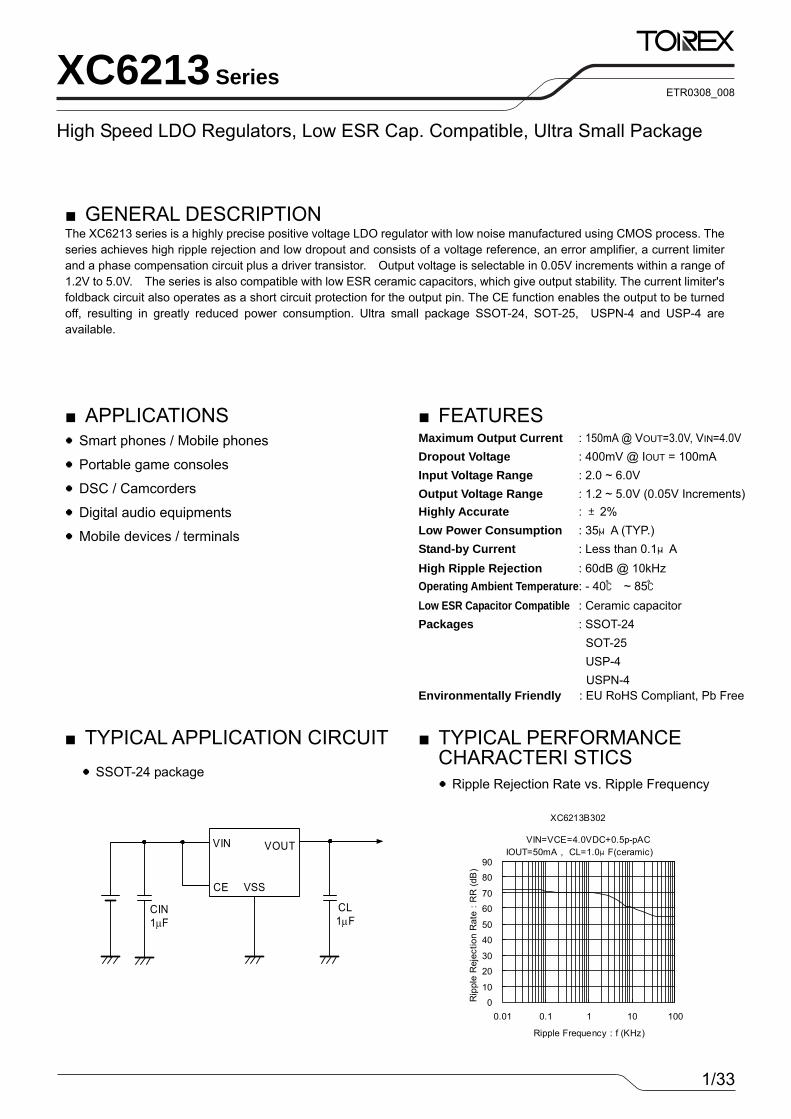
1/33 XC6213 Series High Speed LDO Regulators, Low ESR Cap. Compatible, Ultra Small Package ■GENERAL DESCRIPTION The XC6213 series is a highly precise positive voltage LDO regulator with low noise manufactured using CMOS process. The series achieves high ripple rejection and low dropout and consists of a voltage reference, an error amplifier, a current limiter and a phase compensation circuit plus a driver transistor. Output voltage is selectable in 0.05V increments within a range of 1.2V to 5.0V. The series is also compatible with low ESR ceramic capacitors, which give output stability. The current limiter's foldback circuit also operates as a short circuit protection for the output pin. The CE function enables the output to be turned off, resulting in greatly reduced power consumption. Ultra small package SSOT-24, SOT-25, USPN-4 and USP-4 are available. ■APPLICATIONS ●Smart phones / Mobile phones ●Portable game consoles ●DSC / Camcorders ●Digital audio equipments ●Mobile devices / terminals ■TYPICAL APPLICATION CIRCUIT ■FEATURES Maximum Output Current : 150mA @ VOUT=3.0V, VIN=4.0V Dropout Voltage : 400mV @ IOUT = 100mA Input Voltage Range : 2.0 ~ 6.0V Output Voltage Range : 1.2 ~ 5.0V (0.05V Increments) Highly Accurate : ±2% Low Power Consumption : 35μA (TYP.) Stand-by Current : Less than 0.1μA High Ripple Rejection : 60dB @ 10kHz Operating Ambient Temperature: - 40℃ ~ 85℃ Low ESR Capacitor Compatible : Ceramic capacitor Packages : SSOT-24 SOT-25 USP-4 USPN-4 Environmentally Friendly : EU RoHS Compliant, Pb Free ●SSOT-24 package ■TYPICAL PERFORMANCE CHARACTERI STICS CE VSS VIN VOUT CL 1μF CIN 1μF ●Ripple Rejection Rate vs. Ripple Frequency XC6213B302 0 10 20 30 40 50 60 70 80 90 0.01 0.1 1 10 100 Ripple Frequency : f (KHz) Ripple Rejection Rate : RR (dB) VIN=VCE=4.0VDC+0.5p-pAC IOUT=50mA , CL=1.0μF(ceramic) ETR0308_008
Transcript of XC6213 - Your analog power IC and the best power ... · XC6213 Series solder-plated in recommended...
1/33
XC6213 Series
High Speed LDO Regulators, Low ESR Cap. Compatible, Ultra Small Package
■GENERAL DESCRIPTION The XC6213 series is a highly precise positive voltage LDO regulator with low noise manufactured using CMOS process. The series achieves high ripple rejection and low dropout and consists of a voltage reference, an error amplifier, a current limiter and a phase compensation circuit plus a driver transistor. Output voltage is selectable in 0.05V increments within a range of 1.2V to 5.0V. The series is also compatible with low ESR ceramic capacitors, which give output stability. The current limiter's foldback circuit also operates as a short circuit protection for the output pin. The CE function enables the output to be turned off, resulting in greatly reduced power consumption. Ultra small package SSOT-24, SOT-25, USPN-4 and USP-4 are available.
■APPLICATIONS ●Smart phones / Mobile phones
●Portable game consoles
●DSC / Camcorders
●Digital audio equipments
●Mobile devices / terminals
■TYPICAL APPLICATION CIRCUIT
■FEATURESMaximum Output Current : 150mA @ VOUT=3.0V, VIN=4.0V Dropout Voltage : 400mV @ IOUT = 100mA Input Voltage Range : 2.0 ~ 6.0V Output Voltage Range : 1.2 ~ 5.0V (0.05V Increments)Highly Accurate : ±2% Low Power Consumption : 35μA (TYP.) Stand-by Current : Less than 0.1μA High Ripple Rejection : 60dB @ 10kHz Operating Ambient Temperature: - 40℃ ~ 85℃ Low ESR Capacitor Compatible : Ceramic capacitor Packages : SSOT-24 SOT-25 USP-4 USPN-4 Environmentally Friendly : EU RoHS Compliant, Pb Free
●SSOT-24 package
■TYPICAL PERFORMANCE CHARACTERI STICS
CE VSS
VIN VOUT
CL1μF
CIN1μF
●Ripple Rejection Rate vs. Ripple Frequency
XC6213B302
0
10
20
30
40
50
6070
8090
0.01 0.1 1 10 100
Ripple Frequency : f (KHz)
Rip
ple
Rej
ectio
nR
ate
:RR
(dB
)
VIN=VCE=4.0VDC+0.5p-pACIOUT=50mA , CL=1.0μF(ceramic)
ETR0308_008
2/33
XC6213 Series
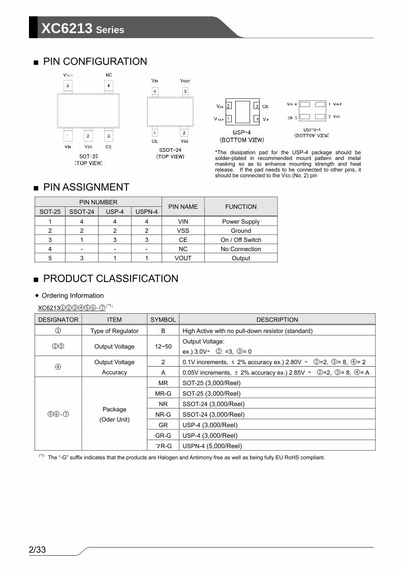
PIN NUMBER SOT-25 SSOT-24 USP-4 USPN-4
PIN NAME FUNCTION
1 4 4 4 VIN Power Supply 2 2 2 2 VSS Ground 3 1 3 3 CE On / Off Switch 4 - - - NC No Connection 5 3 1 1 VOUT Output
DESIGNATOR ITEM SYMBOL DESCRIPTION
① Type of Regulator B High Active with no pull-down resistor (standard)
②③ Output Voltage 12~50 Output Voltage:
ex.) 3.0V→ ② =3, ③= 0
2 0.1V increments, ±2% accuracy ex.) 2.80V → ②=2, ③= 8, ④= 2 ④
Output Voltage
Accuracy A 0.05V increments, ±2% accuracy ex.) 2.85V → ②=2, ③= 8, ④= A
MR SOT-25 (3,000/Reel) MR-G SOT-25 (3,000/Reel)
NR SSOT-24 (3,000/Reel) NR-G SSOT-24 (3,000/Reel) GR USP-4 (3,000/Reel)
GR-G USP-4 (3,000/Reel)
⑤⑥-⑦ Package
(Oder Unit)
7R-G USPN-4 (5,000/Reel)
■PIN CONFIGURATION
■PIN ASSIGNMENT
■PRODUCT CLASSIFICATION●Ordering Information
XC6213①②③④⑤⑥-⑦(*1)
*The dissipation pad for the USP-4 package should be solder-plated in recommended mount pattern and metal masking so as to enhance mounting strength and heat release. If the pad needs to be connected to other pins, it should be connected to the VSS (No. 2) pin
(*1) The “-G” suffix indicates that the products are Halogen and Antimony free as well as being fully EU RoHS compliant.
3/33
XC6213Series
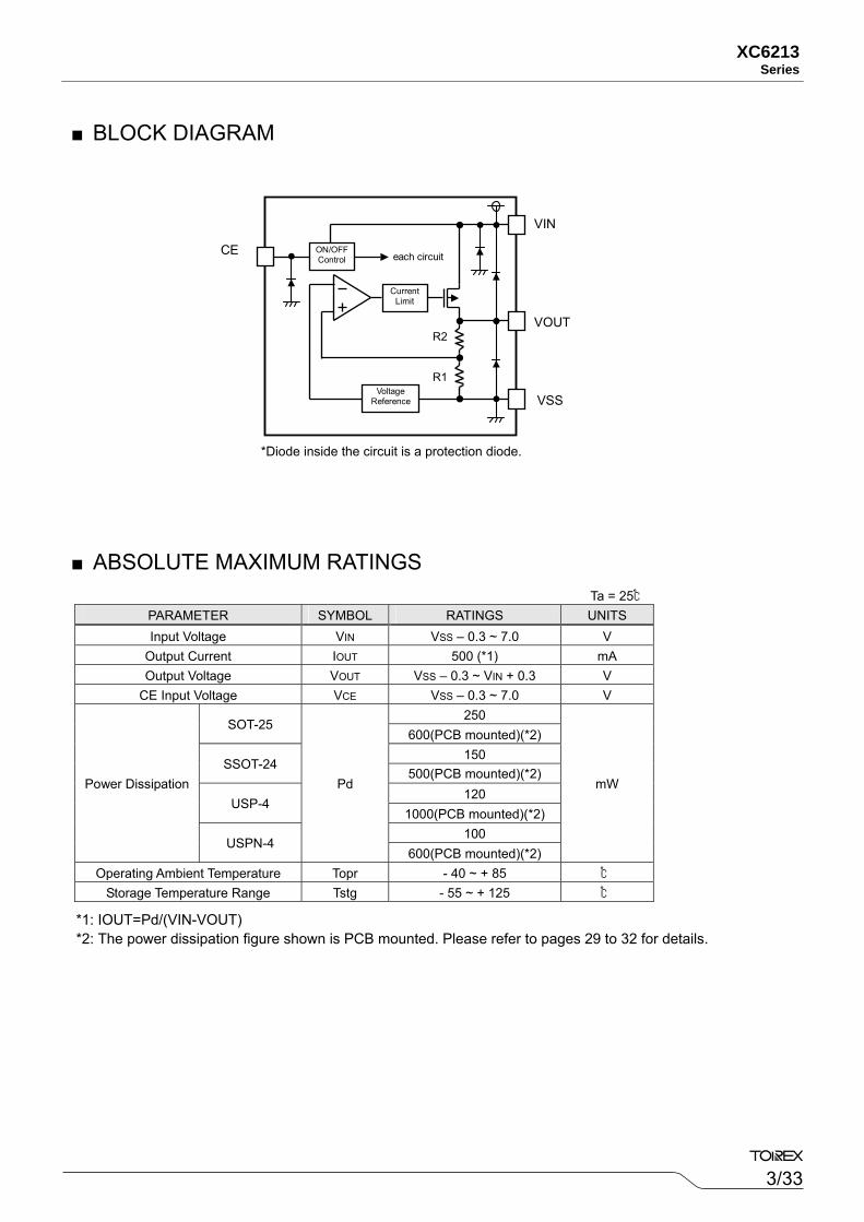
PARAMETER SYMBOL RATINGS UNITS Input Voltage VIN VSS – 0.3 ~ 7.0 V
Output Current IOUT 500 (*1) mA Output Voltage VOUT VSS – 0.3 ~ VIN + 0.3 V
CE Input Voltage VCE VSS – 0.3 ~ 7.0 V 250
SOT-25 600(PCB mounted)(*2)
150 SSOT-24
500(PCB mounted)(*2) 120
USP-4 1000(PCB mounted)(*2)
100
Power Dissipation
USPN-4
Pd
600(PCB mounted)(*2)
mW
Operating Ambient Temperature Topr - 40 ~ + 85 ℃
Storage Temperature Range Tstg - 55 ~ + 125 ℃
■BLOCK DIAGRAM
■ABSOLUTE MAXIMUM RATINGS Ta = 25℃
CurrentLimit
ON/OFF Control
VoltageReference
each circuit
VIN
VOUT
VSS
R2
R1
CE
*Diode inside the circuit is a protection diode.
*1: IOUT=Pd/(VIN-VOUT) *2: The power dissipation figure shown is PCB mounted. Please refer to pages 29 to 32 for details.

4/33
XC6213 Series
PARAMETER SYMBOL CONDITIONS MIN. TYP. MAX. UNITS CIRCUITS
Output Voltage VOUT(E) IOUT=30mA, CE=VIN VOUT(T)
x 0.98VOUT(T)
VOUT(T) x 1.02
V ①
VIN=VOUT(T)+1.0V, VOUT(T)=1.20~1.45V, CE=VIN
100 - -
VIN=VOUT(T)+1.0V, VOUT(T)=1.50~2.95V, CE=VIN
120 - -
VIN=VOUT(T)+1.0V, VOUT(T)=3.00~4.05V, CE=VIN
150 - - Maximum Output Current IOUTMAX
VIN=VOUT(T)+1.0V, VOUT(T)=4.10~5.00V, CE=VIN
200 - -
mA ①
Load Regulation △VOUT VIN=VOUT(T)+1.0V,
1mA≦IOUT≦100mA, CE=VIN- 15 50 mV ①
Vdif1 IOUT = 30mA, CE=VIN E-1 mV ① Dropout Voltage
Vdif2 IOUT=100mA, CE=VIN E-2 mV ①
Supply Current ISS VIN=VOUT(T)+1.0V, CE=VIN 25 35 50 μA ②
Stand-by Current Istby VIN=VOUT(T)+1.0V~6.0V, CE=VSS - 0.01 0.10 μA ②
Line Regulation △VOUT
△VIN ・ VOUT VOUT(T)+1.0V≦VIN≦6V
IOUT=30mA, CE=VIN - 0.01 0.20 %/V ①
Input Voltage VIN - 2.0 - 6.0 V -
Output Voltage Temperature Characteristics
△VOUT △Topr ・ VOUT
IOUT=30mA, CE=VIN - 40℃≦Topr≦85℃
- ±100 - ppm/℃ ①
Ripple Rejection Rate PSRR VIN=[VOUT(T)+1.0 V] +0.5Vp-pAC
IOUT=50mA, f=10kHz, CE=VIN- 60 - dB ③
Short Circuit Current Ishort VIN=VOUT(T) + 1.0V, CE=VIN - 50 - mA ①
CE ‘H’ Level Voltage VCEH - 1.3 - 6.0 V ①
CE ‘L’ Level Voltage VCEL - - - 0.25 V ②
CE ‘H’ Level Current ICEH VCE = VIN=VOUT(T) + 1.0V - 0.1 - 0.1 μA ②
CE ‘L’ Level Current ICEL VIN=VOUT(T) +1.0V, VCE =VSS - 0.1 - 0.1 μA ②
●XC6213B series Ta=25℃
NOTE: *1: VOUT(T): Setting output voltage *2: VOUT(E) = Effective output voltage
(i.e. the output voltage when “VOUT (T) + 1.0V” is provided at the VIN pin while maintaining a certain IOUT value). *3: Vdif = { VIN1
(*5) – VOUT1 (*4)}
*4: VOUT1 = A voltage equal to 98% of the output voltage whenever an amply stabilized IOUT { VOUT(T) + 1.0V } is input. *5: VIN1 = The input voltage when VOUT1 appears as input voltage is gradually decreased. *6: Unless otherwise stated, (VIN = VOUT(T) + 1.0V). *7: VOUT(T)<1.45V = Minimum: VOUT(T)-30mV, Maximum: VOUT(T)+30mV
■ELECTRICAL CHARACTERISTICS

5/33
XC6213Series
Ta=25OC
SYMBOL E-0 E-1 E-2 DROPOUT VOLTAGE 1 DROPTOUT VOLTAGE 2 SETTING
VOLTAGE OUTPUT VOLTAGE
(V) IOUT=30mA (mV) IOUT=100mA (mV) VOUT Vdif1 Vdif1 Vdif2 Vdif2
VOUT(T) MIN. MAX. TYP. MAX. TYP. MAX.
1.20 1.170 1.230 760 800 850 1000 1.25 1.220 1.280 760 800 850 1000 1.30 1.270 1.330 660 700 810 960 1.35 1.320 1.380 660 700 810 960 1.40 1.370 1.430 560 600 770 920 1.45 1.420 1.480 560 600 770 920 1.50 1.470 1.530 460 500 730 880 1.55 1.519 1.581 460 500 730 880 1.60 1.568 1.632 360 400 690 840 1.65 1.617 1.683 360 400 690 840 1.70 1.666 1.734 260 300 650 800 1.75 1.715 1.785 260 300 650 800 1.80 1.764 1.836 200 240 600 750 1.85 1.813 1.887 200 240 600 750 1.90 1.862 1.938 200 240 600 750 1.95 1.911 1.989 200 240 600 750 2.00 1.960 2.040 190 230 530 670 2.05 2.009 2.091 190 230 530 670 2.10 2.058 2.142 190 230 530 670 2.15 2.107 2.193 190 230 530 670 2.20 2.156 2.244 190 230 530 670 2.25 2.205 2.295 190 230 530 670 2.30 2.254 2.346 190 230 530 670 2.35 2.303 2.397 190 230 530 670 2.40 2.352 2.448 190 230 530 670 2.45 2.401 2.499 190 230 530 670 2.50 2.450 2.550 180 210 470 580 2.55 2.499 2.601 180 210 470 580 2.60 2.548 2.652 180 210 470 580 2.65 2.597 2.703 180 210 470 580 2.70 2.646 2.754 180 210 470 580 2.75 2.695 2.805 180 210 470 580 2.80 2.744 2.856 180 210 470 580 2.85 2.793 2.907 180 210 470 580 2.90 2.842 2.958 180 210 470 580 2.95 2.891 3.009 180 210 470 580 3.00 2.940 3.060 150 180 400 500 3.05 2.989 3.111 150 180 400 500 3.10 3.038 3.162 150 180 400 500 3.15 3.087 3.213 150 180 400 500 3.20 3.136 3.264 150 180 400 500 3.25 3.185 3.315 150 180 400 500 3.30 3.234 3.366 150 180 400 500 3.35 2.283 3.417 150 180 400 500 3.40 2.332 3.468 150 180 400 500 3.45 3.381 3.519 150 180 400 500
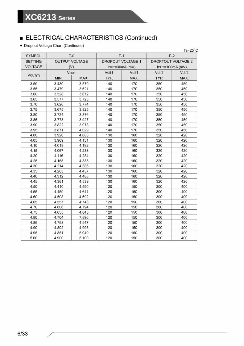
■ELECTRICAL CHARACTERISTICS (Continued)●Dropout Voltage Chart
6/33
XC6213 Series
Ta=25OC
SYMBOL E-0 E-1 E-2 DROPOUT VOLTAGE 1 DROPTOUT VOLTAGE 2 SETTING
VOLTAGE OUTPUT VOLTAGE
(V) IOUT=30mA (mV) IOUT=100mA (mV) VOUT Vdif1 Vdif1 Vdif2 Vdif2
VOUT(T) MIN. MAX. TYP. MAX. TYP. MAX.
3.50 3.430 3.570 140 170 350 450 3.55 3.479 3.621 140 170 350 450 3.60 3.528 3.672 140 170 350 450 3.65 3.577 3.723 140 170 350 450 3.70 3.626 3.774 140 170 350 450 3.75 3.675 3.825 140 170 350 450 3.80 3.724 3.876 140 170 350 450 3.85 3.773 3.927 140 170 350 450 3.90 3.822 3.978 140 170 350 450 3.95 3.871 4.029 140 170 350 450 4.00 3.920 4.080 130 160 320 420 4.05 3.969 4.131 130 160 320 420 4.10 4.018 4.182 130 160 320 420 4.15 4.067 4.233 130 160 320 420 4.20 4.116 4.284 130 160 320 420 4.25 4.165 4.335 130 160 320 420 4.30 4.214 4.386 130 160 320 420 4.35 4.263 4.437 130 160 320 420 4.40 4.312 4.488 130 160 320 420 4.45 4.361 4.539 130 160 320 420 4.50 4.410 4.590 120 150 300 400 4.55 4.459 4.641 120 150 300 400 4.60 4.508 4.692 120 150 300 400 4.65 4.557 4.743 120 150 300 400 4.70 4.606 4.794 120 150 300 400 4.75 4.655 4.845 120 150 300 400 4.80 4.704 7.896 120 150 300 400 4.85 4.753 4.947 120 150 300 400 4.90 4.802 4.998 120 150 300 400 4.95 4.851 5.049 120 150 300 400 5.00 4.900 5.100 120 150 300 400
●Dropout Voltage Chart (Continued)
■ELECTRICAL CHARACTERISTICS (Continued)

7/33
XC6213Series
■TEST CIRCUITS
●Circuit ①
CIN=1.0uF(ceramic)
V
VIN VOUT
VSSCE
CL=1.0uF(ceramic)
RL
A
VV
VIN VOUT
VSSCE
A OPEN
A
CIN=1.0 μF(ceramic)
●Circuit ②
●Circuit ③
VIN VOUT
VSSCE
CL=1.0uF(ceramic )
V
IOUT=50mAVIN={VOUT+1}V DC
+0.25Vp-pAC
V
CIN=1.0μF
(Ceramic)
CIN=1.0μF
(Ceramic)

8/33
XC6213 Series
SETTING VOLTAGE 1.2 ~ 1.75V 1.8 ~ 5.0V CL More than 3.3μF More than 1.0μF
■OPERATIONAL EXPLANATION
■NOTES ON USE
<Output Voltage Regulator Control> The voltage, divided by resistors R1 & R2, which are connected to the VOUT pin is compared with the internal reference voltage by the error amplifier. The P-channel MOSFET which is connected to the VOUT pin is then driven by the subsequent output signal. The output voltage at the VOUT pin is controlled & stabilized by negative feedback. The current limit circuit and short circuit protection operate in relation to the level of output current. Further, the voltage regulator's internal circuitry can be shutdown via the CE pin's signal.
<Low ESR Capacitor> With the XC6213 series regulator, a stable output voltage is achievable even if low ESR capacitors are used, as a phase compensation circuit is built-in to the regulator. In order to ensure the effectiveness of the phase compensation, please connect an output capacitor (CL) with a capacitance, based on the chart below. The equivalent serial resistor (ESR) of the output capacitor (CL) should be within the range as the graph below shown. We also suggest an input capacitor (CIN) of 1.0μF: this should be connected between VIN and VSS in order to stabilize input power source.
Output Capacitor Corresponding Chart
<Short-Circuit Protection> The XC6213 series regulator offers circuit protection by means of a built-in foldback circuit. When the load current reaches the current limit level, the fixed current limiter circuit operates and output voltage drops. As a result of this drop in output voltage, the foldback circuit operates, the output voltage drops further and output current decreases. When the output pin is shorted, a current of about 50mA flows. <CE Pin> The IC's internal regulator circuitry can be shut down via the signal from the CE pin with the XC6213 series. In shutdown mode, output at the VOUT pin will be pulled down to the VSS level. Note that as the XC6213B types are 'High Active / No Pull-Down', operations will become unstable with the CE pin open. We suggest that you use this IC with either a VIN voltage or a VSS voltage input at the CE pin. If this IC is used with the correct specifications for the CE pin, the IC will operate normally. However, supply current may increase as a result of through current in the IC's internal circuitry if a voltage other than VIN or VSS is applied. <Minimum Operating Voltage> Please apply input voltage more than 2.0V or more in order to stabilize the operation of the IC’s. Normal output voltage may not be obtained when the input voltage is lower than 2.0V.
1. Please use this IC within the stated absolute maximum ratings. The IC is liable to malfunction should the ratings be exceeded.
2. Where wiring impedance is high, operations may become unstable due to noise and/or phase lag depending on output current. Please strengthen VIN and VSS wiring in particular.
3. Please wire the input capacitor (CIN) and the output capacitor (CL) as close to the IC as possible. Should rapid input fluctuation or load fluctuation occur, please increase the capacitor value such as CIN or CL to stabilize the operation.
4. Make sure not to use the IC with large current at high temperature. When exceeding power dissipation of a package, heat occurs before short protection operates, and the IC may break.
VSS
VOUT
VINON/OFFControl
Voltage
Reference
each circuitCE
R2
R1
-
+
CurrentLimiter
0.01
0.1
1
10
100
0.01 0.1 1 10 100
ESR
(ohm
)
Ta=-40oC~85
oC
VIN=2.0~6.0V , VOUT=1.2~5.0V,CIN=1.0uF (ceramic)
STABLE REGION
Output Current : IOUT (m A)
Ta=-40℃~85℃
VIN=2.0~6.0V, VOUT=1.2~5.0V, CIN=1.0μF(ceramic)
ES
R (Ω
)

9/33
XC6213Series
■TYPICAL PERFORMANCE CHARACTERISTICS(1) Output Voltage vs. Output Current
XC6213B122
VIN=VCE=2.2V, CIN=1.0μF, CL=3.3μF (ceramic)
XC6213B122
VIN=VCE, Ta=25℃, CIN=1.0μF, CL=3.3μF (ceramic)
XC6213B152
VIN=VCE=2.5V, CIN=1.0μF, CL=3.3μF (ceramic)
XC6213B152
VIN=VCE, Ta=25℃, CIN=1.0,μF CL=3.3μF (ceramic)
XC6213B182
VIN=VCE, Ta=25℃, CIN=CL=1.0μF (ceramic)
XC6213B182
VIN=VCE=2.8V, CIN=CL=1.0μF (ceramic)
VIN=6.0V
VIN=2.1V
VIN=VCE=2.2V, CIN=1.0μF, CL=3.3μF (ceramic) VIN=VCE, Ta=25℃, CIN=1.0μF, CL=3.3μF (ceramic)
Out
put V
olta
ge: V
OU
T (V
)
Output Current: IOUT (mA)
Out
put V
olta
ge: V
OU
T (V
)
Output Current: IOUT (mA)
Out
put V
olta
ge: V
OU
T (V
)
Output Current: IOUT (mA)
Out
put V
olta
ge: V
OU
T (V
)
Output Current: IOUT (mA)
Out
put V
olta
ge: V
OU
T (V
)
Output Current: IOUT (mA)
Out
put V
olta
ge: V
OU
T (V
)
Output Current: IOUT (mA)

10/33
XC6213 Series
■TYPICAL PERFORMANCE CHARACTERISTICS (Continued) (1) Output Voltage vs. Output Current (Continued)
VIN=5.3V
VIN=VCE=4.0V, CIN=CL=1.0μF (ceramic) VIN=VCE, Ta=25℃, CIN=CL=1.0μF (ceramic)
VIN=VCE=6.0V, CIN=CL=1.0μF (ceramic) VIN=VCE, Ta=25℃, CIN=CL=1.0μF (ceramic)
Out
put V
olta
ge: V
OU
T (V
)
Output Current: IOUT (mA)
Out
put V
olta
ge: V
OU
T (V
)
Out
put V
olta
ge: V
OU
T (V
)
Out
put V
olta
ge: V
OU
T (V
)
Output Current: IOUT (mA)
Output Current: IOUT (mA) Output Current: IOUT (mA)

11/33
XC6213Series
■TYPICAL PERFORMANCE CHARACTERISTICS (Continued) (2) Output Voltage vs. Input Voltage
VIN=VCE, Ta=25℃, CIN=1.0μF, CL=3.3μF (ceramic) VIN=VCE, Ta=25℃, CIN=1.0μF, CL=3.3μF (ceramic)
VIN=VCE, Ta=25℃, CIN=CL=1.0μF (ceramic) VIN=VCE, Ta=25℃, CIN=CL=1.0μF (ceramic)
VIN=VCE, Ta=25℃, CIN=CL=1.0μF (ceramic)
Out
put V
olta
ge: V
OU
T (V
)
Input Voltage: VIN (V)
Out
put V
olta
ge: V
OU
T (V
)
Out
put V
olta
ge: V
OU
T (V
)
Out
put V
olta
ge: V
OU
T (V
)
Out
put V
olta
ge: V
OU
T (V
)
Input Voltage: VIN (V)
Input Voltage: VIN (V) Input Voltage: VIN (V)
Input Voltage: VIN (V)

12/33
XC6213 Series
■TYPICAL PERFORMANCE CHARACTERISTICS (Continued) (3) Dropout Voltage vs. Output Current
XC6213B182
VIN=VCE, CIN=1.0μF, CL=3.3μF (ceramic) VIN=VCE, CIN=1.0μF, CL=3.3μF (ceramic)
VIN=VCE, CIN=CL=1.0μF (ceramic)
VIN=VCE, CIN=CL=1.0μF (ceramic)VIN=VCE, CIN=CL=1.0μF (ceramic)
Output Current: IOUT (mA)
Dro
pout
Vol
tage
: Vdi
f (V
)
Dro
pout
Vol
tage
: Vdi
f (V
)
Dro
pout
Vol
tage
: Vdi
f (V
)
Dro
pout
Vol
tage
: Vdi
f (V
)
Dro
pout
Vol
tage
: Vdi
f (V
)
Output Current: IOUT (mA)
Output Current: IOUT (mA) Output Current: IOUT (mA)
Output Current: IOUT (mA)
13/33
XC6213Series
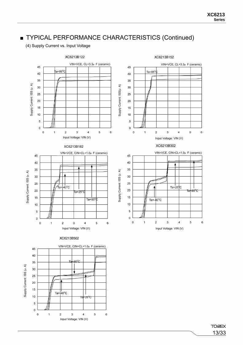
■TYPICAL PERFORMANCE CHARACTERISTICS (Continued) (4) Supply Current vs. Input Voltage
VIN=VCE, CL=3.3μF (ceramic) VIN=VCE, CL=3.3μF (ceramic)
VIN=VCE, CIN=CL=1.0μF (ceramic) VIN=VCE, CIN=CL=1.0μF (ceramic)
VIN=VCE, CIN=CL=1.0μF (ceramic)
Input Voltage: VIN (V)
Sup
ply
Cur
rent
: ISS
(μA)
Sup
ply
Cur
rent
: ISS
(μA
)
Sup
ply
Cur
rent
: ISS
(μA)
Sup
ply
Cur
rent
: ISS
(μA)
Sup
ply
Cur
rent
: ISS
(μA)
Input Voltage: VIN (V)
Input Voltage: VIN (V) Input Voltage: VIN (V)
Input Voltage: VIN (V)
XC6213B182

14/33
XC6213 Series
■TYPICAL PERFORMANCE CHARACTERISTICS (Continued) (5) Output Voltage vs. Ambient Temperature
VIN=VCE=2.2V, CIN=1.0μF, CL=3.3μF(セラミック) VIN=VCE=2.5V, CIN=1.0μF, CL=3.3μF(セラミック) VIN=VCE=2.2V, CIN=1.0μF, CL=3.3μF (ceramic) VIN=VCE=2.5V, CIN=1.0μF, CL=3.3μF (ceramic)
VIN=VCE=2.8V, CIN=CL=1.0μF (ceramic) VIN=VCE=4.0V, CIN=CL=1.0μF (ceramic)
VIN=VCE=6.0 V, CIN=CL=1.0μF (ceramic)
Ambient Temperature: Ta (℃)
Out
put V
olta
ge: V
OU
T (V
)
Out
put V
olta
ge: V
OU
T (V
)
Out
put V
olta
ge: V
OU
T (V
)
Out
put V
olta
ge: V
OU
T (V
)
Out
put V
olta
ge: V
OU
T (V
)
Ambient Temperature: Ta (℃)
Ambient Temperature: Ta (℃) Ambient Temperature: Ta (℃)
Ambient Temperature: Ta (℃)

15/33
XC6213Series
■TYPICAL PERFORMANCE CHARACTERISTICS (Continued) (6) Supply Current vs. Ambient Temperature
(7) CE Threshold Voltage vs. Ambient Temperature
Sup
ply
Cur
rent
ISS
: (μ
A)
Sup
ply
Cur
rent
ISS
: (μ
A)
Sup
ply
Cur
rent
ISS
: (μ
A)
Sup
ply
Cur
rent
ISS
: (μ
A)
Sup
ply
Cur
rent
ISS
: (μ
A)
VIN=VCE=2.2V, CIN=1.0μF, CL=3.3μF(ceramic) VIN=VCE=2.5V, CIN=1.0μF, CL=3.3μF(ceramic)
VIN=VCE=6.0V, CIN=CL=1.0μF(ceramic) VIN=VCE=6.0V, CIN=CL=1.0μF(ceramic)
VIN=VCE=4.0V, CIN=CL=1.0μF(ceramic)VIN=VCE=2.8V, CIN=CL=1.0μF(ceramic)
Ambient Temperature: Ta (℃) Ambient Temperature: Ta (℃)
Ambient Temperature: Ta (℃) Ambient Temperature: Ta (℃)
Ambient Temperature: Ta (℃) Ambient Temperature: Ta (℃)

16/33
XC6213 Series
XC6213B182
-1
0
1
2
3
4
5
時間 (40μsec/div)
入力電圧
VIN
( V
1.75
1.80
1.85
1.90
1.95
2.00
2.05
出力電圧 V
OU
T ( V)
VIN=VCE , Ta=25oC IOUT=1mA、tr=tf=5μsec CL=1.0μF(ceramic)
入力電圧
出力電圧
XC6213B182
-1
0
1
2
3
4
5
時間 (40μsec/div)
入力電圧 V
IN ( V
1.75
1.80
1.85
1.90
1.95
2.00
2.05
出力電圧 V
OU
T ( V)
VIN=VCE , Ta=25oC IOUT=30mA、tr=tf=5μsec CL=1.0μF(ceramic)
入力電圧
出力電圧
XC6213B122
-1
0
1
2
3
4
時間 (40usec/div)
入力電圧 VI
N ( V
1.15
1.20
1.25
1.30
1.35
1.40
出力電圧 VO
UT
( V
VIN=VCE, Ta=25℃ IOUT=1mA , tf=5usecCL=3.3uF(ceramic)
入力電圧
出力電圧
XC6213B122
-1
0
1
2
3
4
時間 (40usec/div)
入力電圧 VI
N ( V
1.15
1.20
1.25
1.30
1.35
1.40
出力電圧 VO
UT
( V
VIN=VCE, Ta=25℃ IOUT=30mA , tf=5usecCL=3.3uF(ceramic)
入力電圧
出力電圧
XC6213B152
-1
0
1
2
3
4
時間 (40usec/div)
入力電圧 VI
N ( V
1.45
1.50
1.55
1.60
1.65
1.70
出力電圧 VO
UT
( V
VIN=VCE, Ta=25℃ IOUT=1mA , tf=5usecCL=3.3uF(ceramic)
入力電圧
出力電圧
XC6213B152
-1
0
1
2
3
4
時間 (40usec/div)
入力電圧 VI
N ( V
1.45
1.50
1.55
1.60
1.65
1.70
出力電圧 VO
UT
( V
VIN=VCE, Ta=25℃ IOUT=30mA , tf=5usecCL=3.3uF(ceramic)
入力電圧
出力電圧
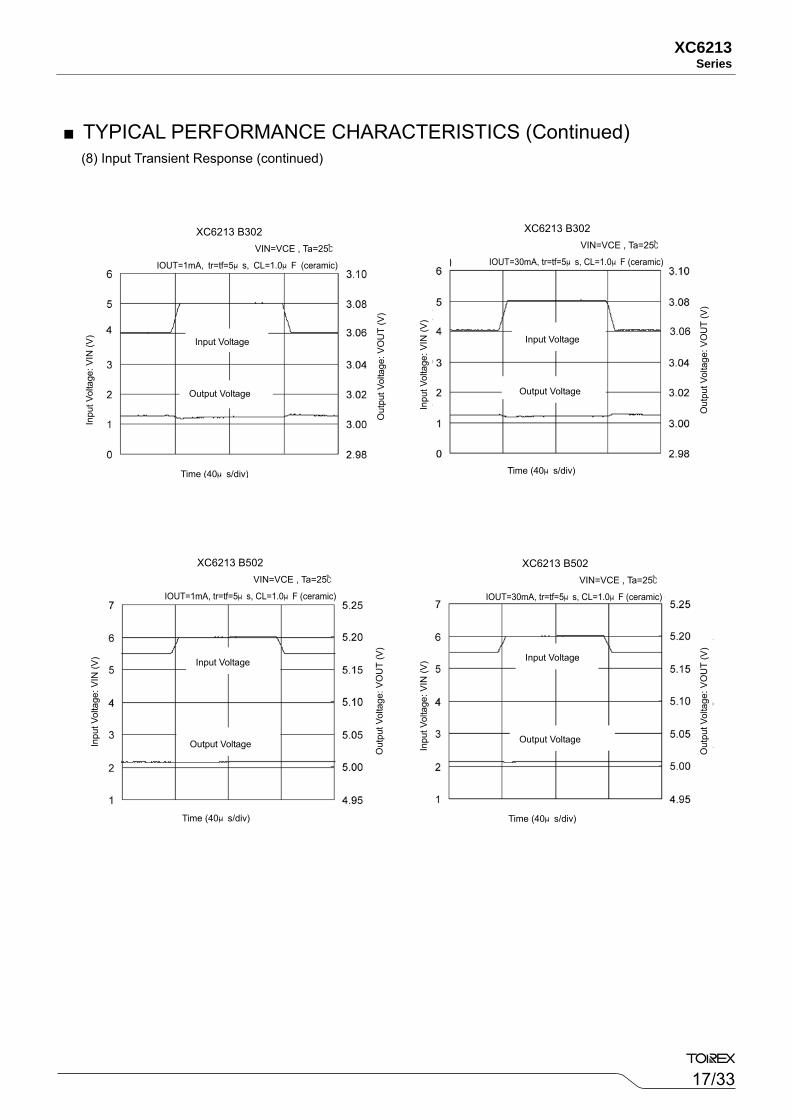
■TYPICAL PERFORMANCE CHARACTERISTICS (Continued) (8) Input Transient Response
Input Voltage
Output Voltage
Inpu
t Vol
tage
: VIN
(V)
Out
put V
olta
ge: V
OU
T (V
)
Inpu
t Vol
tage
: VIN
(V)
Out
put V
olta
ge: V
OU
T (V
)
Time (40μs/div) Time (40μs/div)
Input Voltage
Output Voltage
Time (40μs/div)
Inpu
t Vol
tage
: VIN
(V)
Out
put V
olta
ge: V
OU
T (V
)
Time (40μs/div)
Inpu
t Vol
tage
: VIN
(V)
Input Voltage
Output Voltage
Input Voltage
Output Voltage
Out
put V
olta
ge: V
OU
T (V
)
Input Voltage
Output Voltage Inpu
t Vol
tage
: VIN
(V)
Out
put V
olta
ge: V
OU
T (V
)
Time (40μs/div) Time (40μs/div)
Input Voltage
Output Voltage Inpu
t Vol
tage
: VIN
(V)
Out
put V
olta
ge: V
OU
T (V
)
XC6213 B122
VIN=VCE , Ta=25℃
IOUT=30mA, tr=tf=5μs, CL=3.3μF (ceramic)
XC6213 B122
VIN=VCE , Ta=25℃
IOUT=1mA, tr=tf=5μs, CL=3.3μF (ceramic)
XC6213 B152
VIN=VCE , Ta=25℃
IOUT=30mA, tr=tf=5μs, CL=3.3μF (ceramic)
XC6213 B182
VIN=VCE , Ta=25℃
IOUT=30mA, tr=tf=5μs, CL=1.0μF (ceramic)
XC6213 B152
VIN=VCE , Ta=25℃
IOUT=1mA, tr=tf=5μs, CL=3.3μF (ceramic)
XC6213 B182
VIN=VCE , Ta=25℃
IOUT=1mA, tr=tf=5μs, CL=1.0μF (ceramic)
17/33
XC6213Series
■TYPICAL PERFORMANCE CHARACTERISTICS (Continued) (8) Input Transient Response (continued)
XC6213 B302 VIN=VCE , Ta=25℃
IOUT=1mA, tr=tf=5μs, CL=1.0μF (ceramic)
XC6213 B302 VIN=VCE , Ta=25℃
IOUT=30mA, tr=tf=5μs, CL=1.0μF (ceramic)
XC6213 B502
VIN=VCE , Ta=25℃
IOUT=1mA, tr=tf=5μs, CL=1.0μF (ceramic)
XC6213 B502 VIN=VCE , Ta=25℃
IOUT=30mA, tr=tf=5μs, CL=1.0μF (ceramic)
Time (40μs/div)
Time (40μs/div) Time (40μs/div)
Time (40μs/div)
Inpu
t Vol
tage
: VIN
(V)
Inpu
t Vol
tage
: VIN
(V)
Out
put V
olta
ge: V
OU
T (V
)
Out
put V
olta
ge: V
OU
T (V
)
Input Voltage
Output Voltage
Input Voltage
Output Voltage
Inpu
t Vol
tage
: VIN
(V)
Inpu
t Vol
tage
: VIN
(V)
Out
put V
olta
ge: V
OU
T (V
)
Out
put V
olta
ge: V
OU
T (V
)
Input Voltage
Output Voltage
Input Voltage
Output Voltage

18/33
XC6213 Series
XC6213B182
1.60
1.65
1.70
1.75
1.80
1.85
Time (100μsec/div)
Out
put V
olta
ge :
VOU
T (V
)
0
50
100
150
200
250
Out
put C
urre
nt :
IOU
T (
mA)
Output Voltage
Output Current
Ta=25oC VIN=VCE=2.8V、tr=tf=5μsec CIN= CL=1.0μF(ceramic)
10mA
50mA
XC6213B182
1.60
1.65
1.70
1.75
1.80
1.85
Time (100μsec/div)
Out
put V
olta
ge :
VOU
T (V
)
0
10
20
30
40
50
Out
put C
urre
nt :
IOU
T (
mA)
Ta=25oC VIN=VCE=2.8V、tr=tf=5μsec CIN= CL=1.0μF(ceramic)
Output Current
1mA
10mA
XC6213B122
1.05
1.1
1.15
1.2
1.25
1.3
時間 (100usec/div)
出力電圧
VOU
T (V
)
0
10
20
30
40
50
出力電流
IOU
T (m
A)
1mA
10mA
Ta=25oC VIN=VCE=2.2V、tr=tf=5μsec CIN=1.0uF , CL=3.3μF(ceramic)
Output Voltage
Output Current
XC6213B122
1.05
1.1
1.15
1.2
1.25
1.3
時間 (100usec/div)
出力電圧
VOU
T (V
)0
50
100
150
200
250
出力電流
IOU
T (m
A)
10mA
50mA
Ta=25oC VIN=VCE=2.2V、tr=tf=5μsec CIN=1.0uF , CL=3.3μF(ceramic)
Output Voltage
Output Current
XC6213B152
1.35
1.4
1.45
1.5
1.55
1.6
時間 (100usec/div)
出力電圧
VOU
T (V
)
0
10
20
30
40
50
出力電流
IOU
T (m
A)
1mA
10mA
Ta=25oC VIN=VCE=2.5V、tr=tf=5μsec CIN=1.0uF , CL=3.3μF(ceramic)
Output Voltage
Output Current
XC6213B152
1.35
1.4
1.45
1.5
1.55
1.6
時間 (100usec/div)
出力電圧
VOU
T (V
)
0
50
100
150
200
250
出力電流
IOU
T (m
A)
10mA
50mA
Ta=25oC VIN=VCE=2.5V、tr=tf=5μsec CIN=1.0uF , CL=3.3μF(ceramic)
Output Voltage
Output Current
■TYPICAL PERFORMANCE CHARACTERISTICS (Continued) (9) Load Transient Response
Time (100μs/div)
Out
put V
olta
ge: V
OU
T (V
)
Out
put C
urre
nt: I
OU
T (m
A)
Time (100μs/div)
Time (100μs/div) Time (100μs/div)
Out
put V
olta
ge: V
OU
T (V
)
Out
put C
urre
nt: I
OU
T (m
A)
XC6213 B122
Ta=25℃, VIN=VCE=2.2V, tr=tf=5μs, CIN=CL=3.3μF (ceramic)
XC6213 B122
Ta=25℃, VIN=VCE=2.2V, tr=tf=5μs,CIN=CL=3.3μF (ceramic)
XC6213 B152
Ta=25℃, VIN=VCE=2.5V, tr=tf=5μs, CIN=CL=3.3μF (ceramic)
XC6213 B152
Ta=25℃, VIN=VCE=2.5V, tr=tf=5μs,CIN=CL=3.3μF (ceramic)
XC6213 B182
Ta=25℃, VIN=VCE=2.8V, tr=tf=5μs, CIN=CL=3.3μF (ceramic)
XC6213 B182
Ta=25℃, VIN=VCE=2.8V, tr=tf=5μs,CIN=CL=3.3μF (ceramic)
Time (100μs/div) Time (100μs/div)
Out
put V
olta
ge: V
OU
T (V
)
Out
put V
olta
ge: V
OU
T (V
)
Out
put V
olta
ge: V
OU
T (V
)
Out
put V
olta
ge: V
OU
T (V
)
Out
put C
urre
nt: I
OU
T (m
A)
Out
put C
urre
nt: I
OU
T (m
A)
Out
put C
urre
nt: I
OU
T (m
A)
Out
put C
urre
nt: I
OU
T (m
A)
Output Voltage

19/33
XC6213Series
■TYPICAL PERFORMANCE CHARACTERISTICS (Continued) (9) Load Transient Response (Continued)
XC6213 B302
Ta=25℃, VIN=VCE=4.0V, tr=tf=5μs,
CIN=CL=1.0μF (ceramic)
XC6213 B302 Ta=25℃, VIN=VCE=4.0V, tr=tf=5μs,
CIN=CL=1.0μF (ceramic)
XC6213 B502 Ta=25℃, VIN=VCE=6.0V, tr=tf=5μs,
CIN=CL=1.0μF (ceramic)
XC6213 B502 Ta=25℃, VIN=VCE=6.0V, tr=tf=5μs,
CIN=CL=1.0μF (ceramic)
Time (100μs/div)
Out
put V
olta
ge: V
OU
T (V
)
Out
put C
urre
nt: I
OU
T (m
A)
Time (100μs/div)
Out
put V
olta
ge: V
OU
T (V
)
Out
put C
urre
nt: I
OU
T (m
A)
Out
put V
olta
ge: V
OU
T (V
)
Out
put C
urre
nt: I
OU
T (m
A)
Out
put V
olta
ge: V
OU
T (V
)
Out
put C
urre
nt: I
OU
T (m
A)
Time (100μs/div) Time (100μs/div)
250
5.00
4.95
5.05
4.90
20/33
XC6213 Series
XC6213B182
-6
-4
-2
0
2
4
Time (40μsec/div)
Inpu
t Vol
tage
: VI
N (V
)
0
1
2
3
4
5
Out
put V
olta
ge :
VOU
T (
V)
Ta=25oC IOUT=100μA、tr=tf=5μsec V IN=VCE=0→2.8V CL=1.0μF(ceramic)
Output Voltage
Input Voltage
XC6213B182
-6
-4
-2
0
2
4
Time (40μsec/div)
Inpu
t Vol
tage
: VI
N (V
)
0
1
2
3
4
5
Out
put V
olta
ge :
VOU
T (
V)Input Voltage
Ta=25oC IOUT=30mA、tr=tf=5μsec VIN=VCE=0→2.8V CL=1.0μF(ceramic)
XC6213B122
-1
0
1
2
3
時間 (40usec/div)
入力電圧
VIN
(V)
0
1
2
3
4
出力電圧
VOU
T (V
)
Ta=25oC IOUT=100uA、tr=tf=5usec V IN=VCE=0→2.2V , CL=3.3μF(ceramic)
Input Voltage
Output Voltage
XC6213B122
-1
0
1
2
3
時間 (40usec/div)
入力電圧
VIN
(V)
0
1
2
3
4
出力電圧
VOU
T (V
)
Ta=25oC IOUT=100uA、tr=tf=5usec V IN=VCE=0→2.2V , CL=3.3μF(ceramic)
Input Voltage
Output Voltage
XC6213B152
-1
0
1
2
3
時間 (40usec/div)
入力電圧
VIN
(V)
0
1
2
3
4
出力電圧
VOU
T (V
)
Ta=25oC IOUT=30mA、tr=tf=5usec VIN=VCE=0→2.2V , CL=3.3μF(ceramic)
Input Voltage
Output Voltage
XC6213B152
-1
0
1
2
3
時間 (40usec/div)
入力電圧
VIN
(V)
0
1
2
3
4
出力電圧
VOU
T (V
)
Ta=25oC IOUT=30mA、tr=tf=5usec VIN=VCE=0→2.2V , CL=3.3μF(ceramic)
Input Voltage
Output Voltage
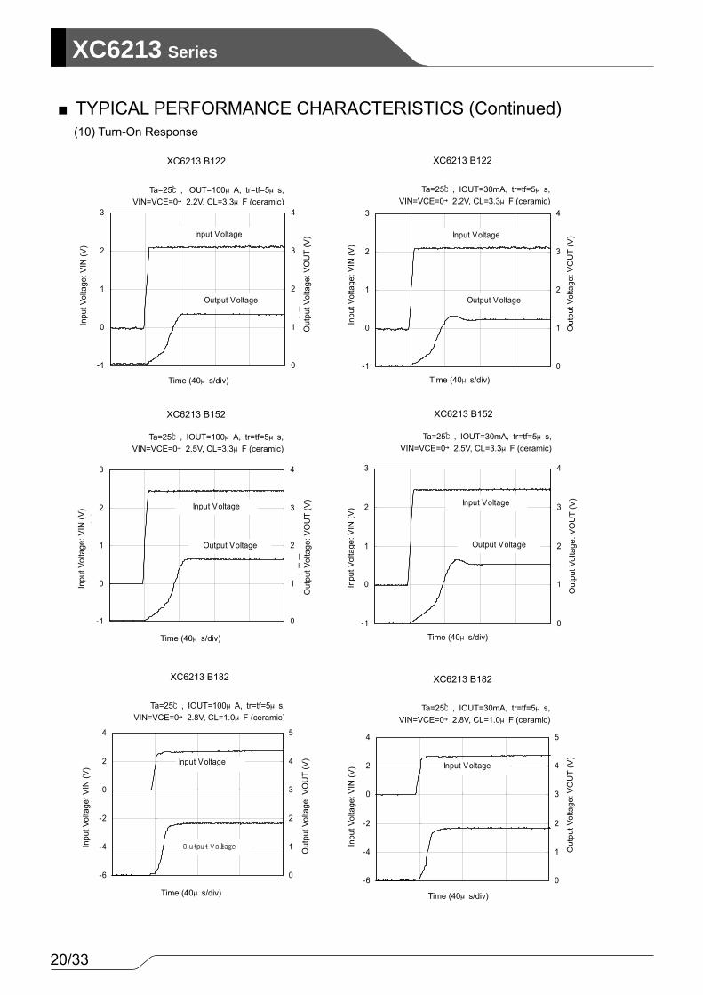
■TYPICAL PERFORMANCE CHARACTERISTICS (Continued) (10) Turn-On Response
XC6213 B122
Ta=25℃, IOUT=100μA, tr=tf=5μs,VIN=VCE=0→2.2V, CL=3.3μF (ceramic)
Time (40μs/div)
Inpu
t Vol
tage
: VIN
(V)
Out
put V
olta
ge: V
OU
T (V
)
Time (40μs/div)
Inpu
t Vol
tage
: VIN
(V)
Out
put V
olta
ge: V
OU
T (V
)
XC6213 B122
Ta=25℃, IOUT=30mA, tr=tf=5μs,VIN=VCE=0→2.2V, CL=3.3μF (ceramic)
XC6213 B152
Ta=25℃, IOUT=100μA, tr=tf=5μs, VIN=VCE=0→2.5V, CL=3.3μF (ceramic)
XC6213 B152
Ta=25℃, IOUT=30mA, tr=tf=5μs,VIN=VCE=0→2.5V, CL=3.3μF (ceramic)
Time (40μs/div)
Inpu
t Vol
tage
: VIN
(V)
Out
put V
olta
ge: V
OU
T (V
)
Time (40μs/div)
Inpu
t Vol
tage
: VIN
(V)
Out
put V
olta
ge: V
OU
T (V
)
XC6213 B182
Ta=25℃, IOUT=100μA, tr=tf=5μs,VIN=VCE=0→2.8V, CL=1.0μF (ceramic)
XC6213 B182
Ta=25℃, IOUT=30mA, tr=tf=5μs,VIN=VCE=0→2.8V, CL=1.0μF (ceramic)
Time (40μs/div)
Inpu
t Vol
tage
: VIN
(V)
Out
put V
olta
ge: V
OU
T (V
)
Time (40μs/div)
Inpu
t Vol
tage
: VIN
(V)
Out
put V
olta
ge: V
OU
T (V
)

21/33
XC6213Series
■TYPICAL PERFORMANCE CHARACTERISTICS (Continued) (10) Turn-On Response (Continued)
XC6213 B302 Ta=25℃, IOUT=100μA, tr=tf=5μs,
VIN=VCE=0→4.0V, CL=1.0μF (ceramic)
XC6213 B302 Ta=25℃, IOUT=30mA, tr=tf=5μs,
VIN=VCE=0→4.0V, CL=1.0μF (ceramic)
XC6213 B502 Ta=25℃, IOUT=100μA, tr=tf=5μs,
VIN=VCE=0→6.0V, CL=1.0μF (ceramic)
XC6213 B302 Ta=25℃, IOUT=30mA, tr=tf=5μs,
VIN=VCE=0→6.0V, CL=1.0μF (ceramic)
Inpu
t Vol
tage
: VIN
(V)
Out
put V
olta
ge: V
OU
T (V
)
Out
put V
olta
ge: V
OU
T (V
)
Out
put V
olta
ge: V
OU
T (V
)
Out
put V
olta
ge: V
OU
T (V
)
Inpu
t Vol
tage
: VIN
(V)
Inpu
t Vol
tage
: VIN
(V)
Inpu
t Vol
tage
: VIN
(V)
Time (40μs/div) Time (40μs/div)
Time (80μs/div) Time (80μs/div)

22/33
XC6213 Series
XC6213B182
-6
-4
-2
0
2
4
Time (40μsec/div)
CE
Inpu
t Vol
tage
: VC
E(V
)
0
1
2
3
4
5
Out
put V
olta
ge :
VOU
T(
V)
Ta=25oC VIN=2.8V , IOUT=100uA、tr=tf=5usec VCE=0.25→1.5V , CL=1.0μF(ceramic)
XC6213B182
-6
-4
-2
0
2
4
Time (40μsec/div)
CE
Inpu
t Vol
tage
: VC
E (V
)
0
1
2
3
4
5
Out
put V
olta
ge :
VOU
T(
V)
Ta=25oC VIN=2.8V , IOUT=30mA、tr=tf=5usec VCE=0.25→1.5V , CL=1.0μF(ceramic)
XC6213B122
-3
-2
-1
0
1
2
時間 (40usec/div)
CE 入力電圧
VCE
(V)
0
1
2
3
4
5
出力電圧
VOU
T (V
)
Ta=25oC VIN=2.2V , IOUT=100uA、tr=tf=5usec VCE=0.25→1.5V , CL=3.3μF(ceramic)
CE Input Voltage
Output Voltage
XC6213B122
-3
-2
-1
0
1
2
時間 (40usec/div)
CE 入力電圧
VCE
(V)
0
1
2
3
4
5
出力電圧
VOU
T (V
)
Ta=25oC VIN=2.2V , IOUT=30mA、tr=tf=5usec VCE=0.25→1.5V , CL=3.3μF(ceramic)
CE Input Voltage
Output Voltage
XC6213B152
-3
-2
-1
0
1
2
時間 (40usec/div)
CE 入力電圧
VCE
(V)
0
1
2
3
4
5
出力電圧
VOU
T (V
)
Ta=25oC V IN=2.5V , IOUT=100uA、tr=tf=5usec VCE=0.25→1.5V , CL=3.3μF(ceramic)
CE Input Voltage
Output Voltage
XC6213B152
-3
-2
-1
0
1
2
時間 (40usec/div)
CE 入力電圧 VCE (V)
0
1
2
3
4
5
出力電圧 VOUT (V)
Ta=25oC VIN=2.5V , IOUT=30mA、tr=tf=5usec VCE=0.25→1.5V , CL=3.3μF(ceramic)
CE Input Voltage
Output Voltage
■TYPICAL PERFORMANCE CHARACTERISTICS (Continued) (11) Enable Response
XC6213 B122 Ta=25℃, VIN=2.2V, IOUT=100μA, tr=tf=5μs,
VCE=0.25→1.5V, CL=3.3μF (ceramic)
Time (40μs/div) Time (40μs/div)
XC6213 B122
Ta=25℃, VIN=2.2V, IOUT=30mA, tr=tf=5μs, VCE=0.25→1.5V, CL=3.3μF (ceramic)
Time (40μs/div) Time (40μs/div)
XC6213 B152
Ta=25℃, VIN=2.5V, IOUT=100μA, tr=tf=5μs, VCE=0.25→1.5V, CL=3.3μF (ceramic)
XC6213 B152
Ta=25℃, VIN=2.5V, IOUT=30mA, tr=tf=5μs, VCE=0.25→1.5V, CL=3.3μF (ceramic)
XC6213 B182
Ta=25℃, VIN=2.8V, IOUT=100μA, tr=tf=5μs, VCE=0.25→1.5V, CL=1.0μF (ceramic)
XC6213 B182
Ta=25℃, VIN=2.8V, IOUT=30mA, tr=tf=5μs, VCE=0.25→1.5V, CL=1.0μF (ceramic)
Time (40μs/div) Time (40μs/div)
Out
put V
olta
ge: V
OU
T (V
)
CE
Inpu
t Vol
tage
: VC
E (V
) C
E In
put V
olta
ge: V
CE
(V)
CE
Inpu
t Vol
tage
: VC
E (V
)
CE
Inpu
t Vol
tage
: VC
E (V
)
CE
Inpu
t Vol
tage
: VC
E (V
) C
E In
put V
olta
ge: V
CE
(V)
Out
put V
olta
ge: V
OU
T (V
)
Out
put V
olta
ge: V
OU
T (V
)
Out
put V
olta
ge: V
OU
T (V
)
Out
put V
olta
ge: V
OU
T (V
) O
utpu
t Vol
tage
: VO
UT
(V)
CE Input Voltage
Output Voltage
CE Input Voltage
Output Voltage

23/33
XC6213Series
■TYPICAL PERFORMANCE CHARACTERISTICS (Continued) (11) Enable Response (Continued)
XC6213 B302
Ta=25℃, VIN=4.0V, IOUT=30mA, tr=tf=5μs,VCE=0.25→1.5V, CL=1.0μF (ceramic)
XC6213 B302
Ta=25℃, VIN=4.0V, IOUT=30mA, tr=tf=5μs,VCE=0.25→1.5V, CL=1.0μF (ceramic)
XC6213 B502
Ta=25℃, VIN=6.0V, IOUT=30mA, tr=tf=5μs,VCE=0.25→1.5V, CL=1.0μF (ceramic)
XC6213 B502
Ta=25℃, VIN=6.0V, IOUT=30mA, tr=tf=5μs,VCE=0.25→1.5V, CL=1.0μF (ceramic)
Time (80μs/div) Time (80μs/div)
Time (40μs/div) Time (40μs/div)
CE
Inpu
t Vol
tage
: VC
E (V
)
CE
Inpu
t Vol
tage
: VC
E (V
)
CE
Inpu
t Vol
tage
: VC
E (V
)
CE
Inpu
t Vol
tage
: VC
E (V
)
Out
put V
olta
ge: V
OU
T (V
)
Out
put V
olta
ge: V
OU
T (V
)
Out
put V
olta
ge: V
OU
T (V
)
Out
put V
olta
ge: V
OU
T (V
)
24/33
XC6213 Series
XC6213B182
0
10
20
30
40
50
60
70
80
90
0.01 0.1 1 10 100
Ripple Frequency : f (KHz)
Rip
ple
Rej
ectio
n R
ate
: RR
VIN=VCE=2.8VDC+0.5p-pAC IOUT=50mA , CL=1.0μF(ceramic)
XC6213B302
0
10
20
30
40
50
60
70
80
90
0.01 0.1 1 10 100
Ripple Frequency : f (KHz)
Rip
ple
Rej
ectio
n R
ate
: RR
VIN=VCE=4.0VDC+0.5p-pAC IOUT=50mA , CL=1.0μF(ceramic)
XC6213B502
0
10
20
30
40
50
60
70
80
90
0.01 0.1 1 10 100
Ripple Frequency : f (KHz)
Rip
ple
Rej
ectio
n R
ate
: RR
VIN=VCE=5.5VDC+0.5p-pAC IOUT=50mA , CL=1.0μF(ceramic)
XC6213B122
0
10
20
30
40
50
60
70
80
90
0.01 0.1 1 10 100
Ripple Frequency : f (KHz)
Rip
ple
Rej
ectio
n R
ate
: RR
VIN=VCE=2.2VDC+0.5p-pAC , IOUT=50mA CIN=0.01uF , CL=3.3uF(ceramic)
XC6213B152
0
10
20
30
40
50
60
70
80
90
0.01 0.1 1 10 100
Ripple Frequency : f (KHz)
Rip
ple
Rej
ectio
n R
ate
: RR
VIN=VCE=2.5VDC+0.5p-pAC , IOUT=50mA CIN=0.01uF , CL=3.3uF(ceramic)
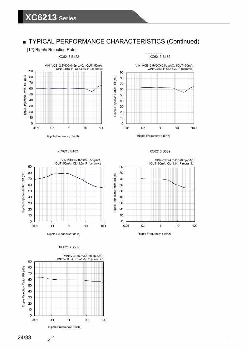
■TYPICAL PERFORMANCE CHARACTERISTICS (Continued) (12) Ripple Rejection Rate
Ripple Frequency: f (kHz)
Rip
ple
Rej
ectio
n R
atio
: RR
(dB
)
Rip
ple
Rej
ectio
n R
atio
: RR
(dB
)
Rip
ple
Rej
ectio
n R
atio
: RR
(dB
)
Rip
ple
Rej
ectio
n R
atio
: RR
(dB
)
Rip
ple
Rej
ectio
n R
atio
: RR
(dB
)
Ripple Frequency: f (kHz)
Ripple Frequency: f (kHz) Ripple Frequency: f (kHz)
Ripple Frequency: f (kHz)
XC6213 B152
VIN=VCE=2.5VDC+0.5p-pAC, IOUT=50mA, CIN=0.01μF, CL=3.3μF (ceramic)
XC6213 B122
VIN=VCE=2.2VDC+0.5p-pAC, IOUT=50mA,CIN=0.01μF, CL=3.3μF (ceramic)
XC6213 B302
VIN=VCE=4.0VDC+0.5p-pAC, IOUT=50mA, CL=1.0μF (ceramic)
XC6213 B182
VIN=VCE=2.8VDC+0.5p-pAC, IOUT=50mA, CL=1.0μF (ceramic)
XC6213 B502
VIN=VCE=5.5VDC+0.5p-pAC,IOUT=50mA, CL=1.0μF (ceramic)
25/33
XC6213Series
●SOT-25 ●SSOT-24
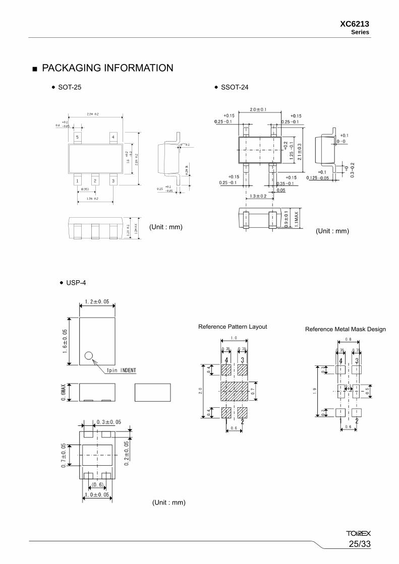
■PACKAGING INFORMATION
●USP-4
Reference Pattern Layout Reference Metal Mask Design
1 3
2.9±0.2
0.4+0.1-0.05
1.6+0.2-0.1
1.9±0.2
2.8±0.2
1.1±0.1
1.3MAX
0.15+0.1-0.05
0.2MIN
0~0.1
2
5 4
(0.95)
(Unit : mm) (Unit : mm)
(Unit : mm)
26/33
XC6213 Series
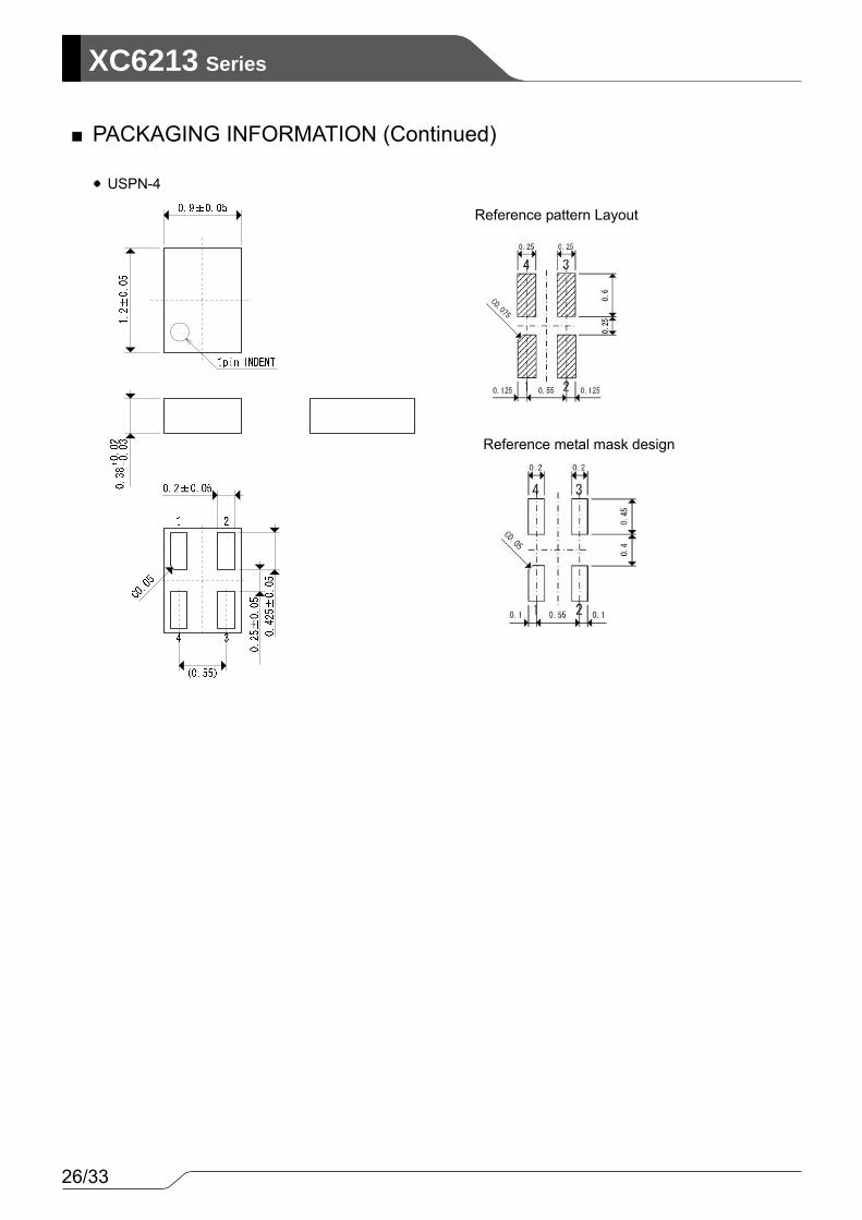
■PACKAGING INFORMATION (Continued)
●USPN-4
Reference pattern Layout
Reference metal mask design

27/33
XC6213Series
MARK VOLTAGE (V) PRODUCT SERIES 3 3.X XC6213B3xxNx 5 5.X XC6213B5xxNx
MARK PRODUCT SERIES C XC6213xxxxxx
MARK VOLTAGE=0.1~3.0V
VOLTAGE=3.1~6.0V
VOLTAGE=0.15~3.05V
VOLTAGE=3.15~6.05V
PRODUCT SERIES
X B F M XC6213xxxxxx
MARK OUTPUT VOLTAGE (V) MARK OUTPUT VOLTAGE (V)
0 - 3.1 - 3.15 F 1.6 4.6 1.65 4.65 1 - 3.2 - 3.25 H 1.7 4.7 1.75 4.75 2 - 3.3 - 3.35 K 1.8 4.8 1.85 4.85 3 - 3.4 - 3.45 L 1.9 4.9 1.95 4.95 4 - 3.5 - 3.55 M 2.0 5.0 2.05 - 5 - 3.6 - 3.65 N 2.1 - 2.15 - 6 - 3.7 - 3.75 P 2.2 - 2.25 - 7 - 3.8 - 3.85 R 2.3 - 2.35 - 8 - 3.9 - 3.95 S 2.4 - 2.45 - 9 - 4.0 - 4.05 T 2.5 - 2.55 - A - 4.1 - 4.15 U 2.6 - 2.65 - B 1.2 4.2 1.25 4.25 V 2.7 - 2.75 - C 1.3 4.3 1.35 4.35 X 2.8 - 2.85 - D 1.4 4.4 1.45 4.45 Y 2.9 - 2.95 - E 1.5 4.5 1.55 4.55 Z 3.0 - 3.05 -
MARK VOLTAGE
(V) PRODUCT SERIES MARK
VOLTAGE (V)
PRODUCT SERIES
0 X.0 XC6213Bx0xNx A X.05 XC6213Bx0ANx1 X.1 XC6213Bx1xNx B X.15 XC6213Bx1ANx2 X.2 XC6213Bx2xNx C X.25 XC6213Bx2ANx3 X.3 XC6213Bx3xNx D X.35 XC6213Bx3ANx4 X.4 XC6213Bx4xNx E X.45 XC6213Bx4ANx5 X.5 XC6213Bx5xNx F X.55 XC6213Bx5ANx6 X.6 XC6213Bx6xNx H X.65 XC6213Bx6ANx7 X.7 XC6213Bx7xNx K X.75 XC6213Bx7ANx8 X.8 XC6213Bx8xNx L X.85 XC6213Bx8ANx9 X.9 XC6213Bx9xNx M X.95 XC6213Bx9ANx
■MARKING RULE① represents product series
②③ represents type of regulator
④ represents production lot number 0 to 9, to Z reverse character 0 to 9, A to Z repeated (G, I, J, O, Q, W excluded)
③ represents output voltage
① represents integer of output voltage
② represents decimal point of output voltage
④ represents production lot number 0 to 9, A to Z repeated (G, I, J, O, Q, W excluded). Note: No character inversion used.
USP-4 (TOP VIEW)
① ② ③ ④
1 2 3
5 4
SOT-25 (TOP VIEW)
●SOT-25 & USP-4
●SSOT-24
① ② ④
1 2
34
SSOT-24 (SC-82) (TOP VIEW)
28/33
XC6213 Series
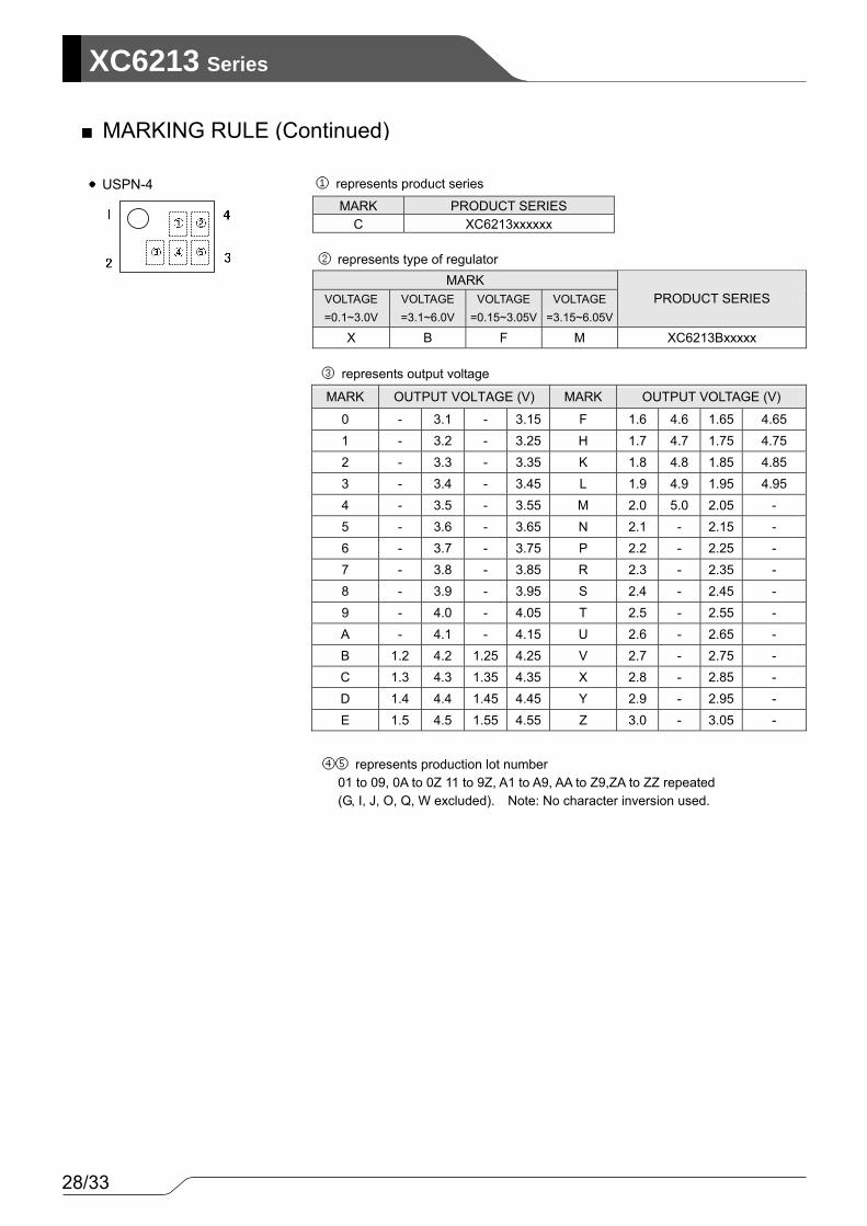
MARK PRODUCT SERIES C XC6213xxxxxx
MARK VOLTAGE=0.1~3.0V
VOLTAGE=3.1~6.0V
VOLTAGE=0.15~3.05V
VOLTAGE=3.15~6.05V
PRODUCT SERIES
X B F M XC6213Bxxxxx
MARK OUTPUT VOLTAGE (V) MARK OUTPUT VOLTAGE (V)
0 - 3.1 - 3.15 F 1.6 4.6 1.65 4.65 1 - 3.2 - 3.25 H 1.7 4.7 1.75 4.75 2 - 3.3 - 3.35 K 1.8 4.8 1.85 4.85 3 - 3.4 - 3.45 L 1.9 4.9 1.95 4.95 4 - 3.5 - 3.55 M 2.0 5.0 2.05 - 5 - 3.6 - 3.65 N 2.1 - 2.15 - 6 - 3.7 - 3.75 P 2.2 - 2.25 - 7 - 3.8 - 3.85 R 2.3 - 2.35 - 8 - 3.9 - 3.95 S 2.4 - 2.45 - 9 - 4.0 - 4.05 T 2.5 - 2.55 - A - 4.1 - 4.15 U 2.6 - 2.65 - B 1.2 4.2 1.25 4.25 V 2.7 - 2.75 - C 1.3 4.3 1.35 4.35 X 2.8 - 2.85 - D 1.4 4.4 1.45 4.45 Y 2.9 - 2.95 - E 1.5 4.5 1.55 4.55 Z 3.0 - 3.05 -
■MARKING RULE (Continued)
●USPN-4 ① represents product series
② represents type of regulator
③ represents output voltage
④⑤ represents production lot number 01 to 09, 0A to 0Z 11 to 9Z, A1 to A9, AA to Z9,ZA to ZZ repeated (G, I, J, O, Q, W excluded). Note: No character inversion used.

29/33
XC6213Series
● SOT-25 Power Dissipation Board Mount (Tj max = 125℃)
Ambient Temperature(℃) Power Dissipation Pd(mW) Thermal Resistance (℃/W)
25 600
85 240 166.67
Pd-Ta特性グラフ
0
100
200
300
400
500
600
700
25 45 65 85 105 125
周辺温度Ta(℃)
許容損失Pd(mW)
Power dissipation data for the SOT-25 is shown in this page. The value of power dissipation varies with the mount board conditions.Please use this data as one of reference data taken in the described condition.
1. Measurement Condition (Reference data) Condition: Mount on a board Ambient: Natural convection Soldering: Lead (Pb) free Board: Dimensions 40 x 40 mm (1600 mm2 in one side)
Copper (Cu) traces occupy 50% of the board area In top and back faces Package heat-sink is tied to the copper traces (Board of SOT-26 is used.)
Material: Glass Epoxy (FR-4) Thickness: 1.6 mm Through-hole: 4 x 0.8 Diameter
2. Power Dissipation vs. Ambient temperature
Pd vs. Ta
Ambient Temperature Ta (℃)
Pow
er D
issi
patio
n Pd
(mW
)
評価基板レイアウト(単位:mm)Evaluation Board (Unit: mm)
30/33
XC6213 Series
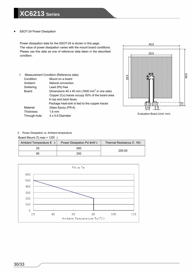
● SSOT-24 Power Dissipation
Board Mount (Tj max = 125℃)
Ambient Temperature(℃) Power Dissipation Pd(mW) Thermal Resistance (℃/W)
25 500
85 200 200.00
Power dissipation data for the SSOT-24 is shown in this page. The value of power dissipation varies with the mount board conditions.Please use this data as one of reference data taken in the described condition.
1. Measurement Condition (Reference data) Condition: Mount on a board Ambient: Natural convection Soldering: Lead (Pb) free Board: Dimensions 40 x 40 mm (1600 mm2 in one side)
Copper (Cu) traces occupy 50% of the board area In top and back faces Package heat-sink is tied to the copper traces
Material: Glass Epoxy (FR-4) Thickness: 1.6 mm Through-hole: 4 x 0.8 Diameter
2. Power Dissipation vs. Ambient temperature
Evaluation Board (Unit: mm)

31/33
XC6213Series
● USP-4 Power Dissipation
Board Mount (Tj max = 125℃)
Ambient Temperature(℃) Power Dissipation Pd(mW) Thermal Resistance (℃/W)
25 1000
85 400 100.00
Power dissipation data for the USP-4 is shown in this page. The value of power dissipation varies with the mount board conditions.Please use this data as one of reference data taken in the described condition.
Evaluation Board (Unit: mm)
1. Measurement Condition (Reference data) Condition: Mount on a board Ambient: Natural convection Soldering: Lead (Pb) free Board: Dimensions 40 x 40 mm (1600 mm2 in one side)
Copper (Cu) traces occupy 50% of the board area In top and back faces Package heat-sink is tied to the copper traces
Material: Glass Epoxy (FR-4) Thickness: 1.6 mm Through-hole: 4 x 0.8 Diameter
2. Power Dissipation vs. Ambient temperature
40.0
28.9
1.42.54
32/33
XC6213 Series
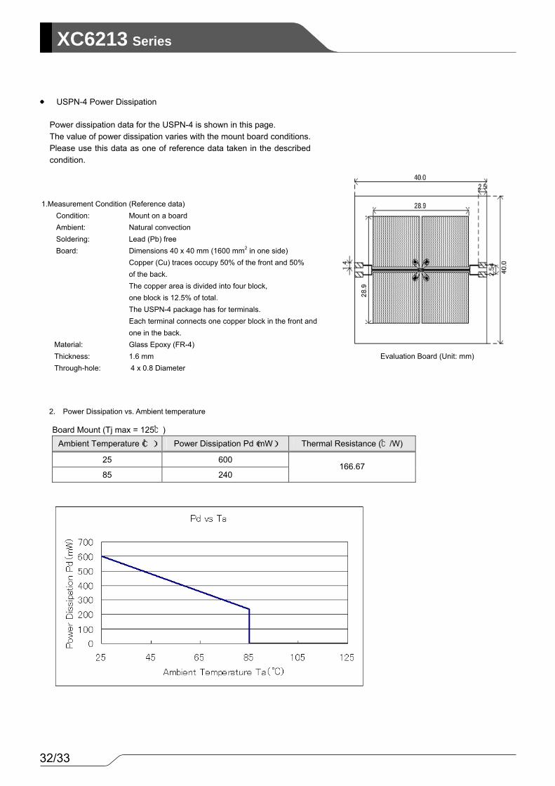
● USPN-4 Power Dissipation
Board Mount (Tj max = 125℃)
Ambient Temperature(℃) Power Dissipation Pd(mW) Thermal Resistance (℃/W)
25 600
85 240 166.67
Power dissipation data for the USPN-4 is shown in this page. The value of power dissipation varies with the mount board conditions.Please use this data as one of reference data taken in the described condition.
Evaluation Board (Unit: mm)
1.Measurement Condition (Reference data) Condition: Mount on a board Ambient: Natural convection Soldering: Lead (Pb) free Board: Dimensions 40 x 40 mm (1600 mm2 in one side)
Copper (Cu) traces occupy 50% of the front and 50% of the back.
The copper area is divided into four block, one block is 12.5% of total. The USPN-4 package has for terminals. Each terminal connects one copper block in the front and
one in the back. Material: Glass Epoxy (FR-4) Thickness: 1.6 mm Through-hole: 4 x 0.8 Diameter
2. Power Dissipation vs. Ambient temperature

33/33
XC6213Series
1. The products and product specifications contained herein are subject to change without
notice to improve performance characteristics. Consult us, or our representatives
before use, to confirm that the information in this datasheet is up to date.
2. We assume no responsibility for any infringement of patents, patent rights, or other
rights arising from the use of any information and circuitry in this datasheet.
3. Please ensure suitable shipping controls (including fail-safe designs and aging
protection) are in force for equipment employing products listed in this datasheet.
4. The products in this datasheet are not developed, designed, or approved for use with
such equipment whose failure of malfunction can be reasonably expected to directly
endanger the life of, or cause significant injury to, the user.
(e.g. Atomic energy; aerospace; transport; combustion and associated safety
equipment thereof.)
5. Please use the products listed in this datasheet within the specified ranges.
Should you wish to use the products under conditions exceeding the specifications,
please consult us or our representatives.
6. We assume no responsibility for damage or loss due to abnormal use.
7. All rights reserved. No part of this datasheet may be copied or reproduced without the
prior permission of TOREX SEMICONDUCTOR LTD.