X-ray Scattering Investigations Of Metallic Thin Films
144
University of Central Florida University of Central Florida STARS STARS Electronic Theses and Dissertations, 2004-2019 2013 X-ray Scattering Investigations Of Metallic Thin Films X-ray Scattering Investigations Of Metallic Thin Films Andrew Warren University of Central Florida Part of the Materials Science and Engineering Commons Find similar works at: https://stars.library.ucf.edu/etd University of Central Florida Libraries http://library.ucf.edu This Doctoral Dissertation (Open Access) is brought to you for free and open access by STARS. It has been accepted for inclusion in Electronic Theses and Dissertations, 2004-2019 by an authorized administrator of STARS. For more information, please contact [email protected]. STARS Citation STARS Citation Warren, Andrew, "X-ray Scattering Investigations Of Metallic Thin Films" (2013). Electronic Theses and Dissertations, 2004-2019. 2591. https://stars.library.ucf.edu/etd/2591
Transcript of X-ray Scattering Investigations Of Metallic Thin Films

University of Central Florida University of Central Florida
STARS STARS
Electronic Theses and Dissertations, 2004-2019
2013
X-ray Scattering Investigations Of Metallic Thin Films X-ray Scattering Investigations Of Metallic Thin Films
Andrew Warren University of Central Florida
Part of the Materials Science and Engineering Commons
Find similar works at: https://stars.library.ucf.edu/etd
University of Central Florida Libraries http://library.ucf.edu
This Doctoral Dissertation (Open Access) is brought to you for free and open access by STARS. It has been accepted
for inclusion in Electronic Theses and Dissertations, 2004-2019 by an authorized administrator of STARS. For more
information, please contact [email protected].
STARS Citation STARS Citation Warren, Andrew, "X-ray Scattering Investigations Of Metallic Thin Films" (2013). Electronic Theses and Dissertations, 2004-2019. 2591. https://stars.library.ucf.edu/etd/2591

X-RAY SCATTERING INVESTIGATIONS OF METALLIC THIN FILMS
by
ANDREW P. WARREN B. S. Physics, University of Central Florida, 2004
A dissertation submitted in partial fulfillment of the requirements for the degree of Doctor of Philosophy
in the Department of Materials Science and Engineering in the College of Engineering and Computer Science
at the University of Central Florida Orlando, Florida
Spring Term 2013
Major Professor: Kevin R. Coffey

ii
2013 Andrew P. Warren

iii
ABSTRACT
Nanometric thin films are used widely throughout various industries and for
various applications. Metallic thin films, specifically, are relied upon extensively in the
microelectronics industry, among others. For example, alloy thin films are being
investigated for CMOS applications, tungsten films find uses as contacts and diffusion
barriers, and copper is used often as interconnect material. Appropriate metrology
methods must therefore be used to characterize the physical properties of these films. X-
ray scattering experiments are well suited for the investigation of nano-scaled systems,
and are the focus of this doctoral dissertation. Emphasis is placed on (1) phase
identification of polycrystalline thin films, (2) the evaluation of the grain size and
microstrain of metallic thin films by line profile analysis, and (3) the study of
morphological evolution in solid/solid interfaces.
To illustrate the continued relevance of x-ray diffraction for phase identification
of simple binary alloy systems, Pt-Ru thin films, spanning the compositional range from
pure Pt to pure Ru were investigated. In these experiments, a meta-stable extension of
the HCP phase is observed in which the steepest change in the electronic work function
coincides with a rapid change in the c/a ratio of the HCP phase.
For grain size and microstrain analysis, established line profile methods are
discussed in terms of Cu and W thin film analysis. Grain sizes obtained by x-ray
diffraction are compared to transmission electron microscopy based analyses. Significant
discrepancies between x-ray and electron microscopy are attributed to sub-grain
misorientations arising from dislocation core spreading at the film/substrate interface. A
novel "residual" full width half max parameter is introduced for examining the

iv
contribution of strain to x-ray peak broadening. The residual width is subsequently used
to propose an empirical method of line profile analysis for thin films on substrates.
X-ray reflectivity was used to study the evolution of interface roughness with
annealing for a series of Cu thin
films that were encapsulated in both SiO2 and Ta/SiO2. While all samples follow similar
growth dynamics, notable differences in the roughness evolution with high temperature
ex-situ annealing were observed. The annealing resulted in a smoothing of only one
interface for the SiO2 encapsulated films, while neither interface of the Ta/SiO2
encapsulated films evolved significantly. The fact that only the upper Cu/SiO2 interface
evolves is attributed to mechanical pinning of the lower interface to the rigid substrate.
The lack of evolution of the Cu/Ta/SiO2 interface is consistent with the lower diffusivity
expected of Cu in a Cu/Ta interface as compared to that in a Cu/SiO2 interface. The
smoothing of the upper Cu/SiO2 interface qualitatively follows that expected for
capillarity driven surface diffusion but with notable quantitative deviation.

v
Dedicated to my loving parents, Kalina and Andy.
Dziękuję Wam za rady, zrozumienie, i oparcie. Również dziękuję Wam za Waszą
miłość i wiarę w moje możliwości. Kocham Was bardzo!!!

vi
ACKNOWLEDGMENTS
I am grateful to acknowledge the financial support of the Semiconductor Research
Corporation, Task No. 2121.001 and 1292.008.
Additionally, portions of this research were carried out at the Stanford
Synchrotron Radiation Lightsource, a national user facility operated by Stanford
University on behalf of the U.S. Department of Energy, Office of Basic Energy Sciences.
Similarly, portions of this research were conducted at the Center for Nanophase Materials
Sciences, which is sponsored at Oak Ridge National Laboratory by the Scientific User
Facilities Division, Office of Basic Energy Sciences, U.S. Department of Energy.
I am also grateful to acknowledge the International Centre for Diffraction Data for
their support in the form of the 2010 and 2011 Ludo Frevel Crystallography Scholarships.
Similarly, the IEEE Electron Device Society, for their support in the form of the 2007
Masters Fellowship.
I would also like to thank the many faculty, staff, friends, and collogues who have
made the graduate experience at UCF worthwhile and possible. I wish to specifically
thank my advisor, Dr. Kevin R. Coffey, and the AMPAC support staff: Kari Stiles,
Angelina Feliciano, Cindy Harle, Karen Glidewell, Edward Dein, Kirk Scammon, and
Mikhail Klimov. Also warranting many thanks are my committee members: Dr Katayun
Barmak, Dr. Helge H. Heinrich, Dr. Yongho Sohn, Dr. Challapalli Suryanarayana, and
Dr. Micheal F. Toney. Furthermore, the works presented here would not have been
possible without the collaborating efforts of Ravi Todi, Tik Sun, Bo Yao, Amith Darbal,
Dooho Choi and Xuan Liu.

vii
On a personal note, having been diagnosed with Addison's Disease early in my
graduate career, I wish to thank the National Adrenal Disease Foundation for providing
support, information and education to individuals with diseases of the adrenal glands.
Most importantly, I would like to express my utmost gratitude to my Parents;
Kalina and Andy Warren, to whom this dissertation is dedicated. Also my sister Karina,
and of course my better half, Melissa.

viii
TABLE OF CONTENTS
LIST OF FIGURES ........................................................................................................... xi
LIST OF TABLES............................................................................................................ xv
CHAPTER ONE : INTRODUCTION AND SCATTERING THEORY.......................... 1
1.1 X-ray Scattering Theory: Diffraction....................................................................... 1
1.1.1 Phase Identification............................................................................................ 1
1.1.2 Grain Size Analysis............................................................................................ 2
1.1.2.1 Peak Broadening ......................................................................................... 2
1.1.2.2 Scherrer Equation........................................................................................ 7
1.1.2.3 Williamson-Hall plot ................................................................................ 11
1.2 X-ray Scattering Theory: Reflectivity ................................................................... 16
1.2.1 Surface Statistics.............................................................................................. 16
1.2.2 Surface and Interface Kinetics ......................................................................... 21
1.2.3 X-Ray Reflectivity ........................................................................................... 25
CHAPTER TWO : EXPERIMENTAL DETAILS.......................................................... 28
2.1 Pt-Ru ....................................................................................................................... 28
2.1.1 Sample preparation .......................................................................................... 28
2.1.2 X-ray Scattering ............................................................................................... 29
2.1.3 Additional Characterization ............................................................................. 32
2.2 Encapsulated Cu and W.......................................................................................... 32
2.2.1 Sample preparation .......................................................................................... 32
2.2.2 X-ray Scattering ............................................................................................... 34

ix
2.2.2.1 X-ray Diffraction ...................................................................................... 34
2.2.2.2 X-ray Reflectivity ..................................................................................... 38
2.2.3 Additional Characterization ............................................................................. 39
2.3 GlobalFoundries W................................................................................................. 40
2.3.1 Sample Preparation .......................................................................................... 40
2.3.2 X-ray Scattering ............................................................................................... 40
2.3.3 Additional Characterization ............................................................................. 41
CHAPTER THREE : METASTABLE PHASE IDENTIFICATION ............................. 43
3.1 Objectives ............................................................................................................... 43
3.2 Results..................................................................................................................... 44
3.3 Conclusion .............................................................................................................. 51
CHAPTER FOUR : GRAIN SIZE AND DEFECT ANALYSIS.................................... 52
4.1 Objectives ............................................................................................................... 56
4.2 Results of Scherrer Analysis................................................................................... 56
4.2.1 Grain Size......................................................................................................... 58
4.2.2 Shape Factor..................................................................................................... 59
4.3 Results of Williamson-Hall Analysis...................................................................... 63
4.3.1 Classical Williamson-Hall ............................................................................... 64
4.3.2 Modified Williamson-Hall............................................................................... 67
4.4 Effects of Microstrain ............................................................................................. 69
4.4.1 Residual FWHM .............................................................................................. 70
4.4.2 Dislocation Core Spreading ............................................................................. 75
4.4.3 Intra-Grain Misorientations ............................................................................. 81

x
4.5 Empirical Grain Size Calculation; A Novel Line Profile Method.......................... 88
4.6 Conclusion .............................................................................................................. 93
CHAPTER FIVE : INTERFACE MORPHOLGY ANALYSIS ..................................... 95
5.1 Objectives ............................................................................................................... 95
5.2 Results..................................................................................................................... 95
5.2.1 Qualitative Observations.................................................................................. 95
5.2.2 Statistical Characterization of Film Growth .................................................... 99
5.2.3 Interface Smoothening ................................................................................... 105
5.3 Conclusions........................................................................................................... 113
CHAPTER SIX : SUMMARY ....................................................................................... 115
CHAPTER SEVEN : FUTURE WORK........................................................................ 117
7.1 Future work in grain size and microstructural analysis of metallic thin films...... 117
7.2 Future investigations into the morphological stability of interfaces..................... 118
REFERENCES ............................................................................................................... 122

xi
LIST OF FIGURES
Figure 1 Instrumental Broadening ...................................................................................... 4
Figure 2 Effect of strain on x-ray peak profile ................................................................... 5
Figure 3 Size Broadening.................................................................................................... 9
Figure 4 Classical Williamson-Hall plot........................................................................... 12
Figure 5 Modified Williamson-Hall plot .......................................................................... 13
Figure 6 Schematic representation of dislocation contrast ............................................... 15
Figure 7 Self-similar scaling (a and b) and self-affine scaling (c and d).......................... 19
Figure 8 Idealized solid-solid interface of wavelength λ................................................. 22
Figure 9 GIXRD Geometry: i remains constant, the detector scans a range 2θ.......... 29
Figure 10 GIXRD trace through reciprocal space ............................................................ 31
Figure 11 GID Geometry: i and f are small and equal, and approximately equal to .
Q remains in the plane. ..................................................................................................... 35
Figure 12 Dependence of αi on and ........................................................................... 36
Figure 13 GID trace through reciprocal space with constant αi........................................ 37
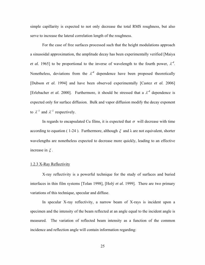
Figure 14 GID trace through reciprocal space with constant ........................................ 41
Figure 15 Pt-Ru GIXRD ................................................................................................... 45
Figure 16 Ru 58% alloy GIXRD ...................................................................................... 46
Figure 17 Variation in lattice spacing with Ru concentration .......................................... 47
Figure 18 Effect of composition on c/a ratio in HCP Pt-Ru films.................................... 48
Figure 19 Nonlinear work-function response to Ru concentration................................... 49
Figure 20 Dependence of Pt-Ru Work Function on c/a ratio of HCP phase .................... 50
Figure 21 Experimental and simulated (a) Cu and (b) W GID profiles........................... 53

xii
Figure 22 Scherrer and TEM Grain Size Comparison...................................................... 59
Figure 23 Optimized Scherrer shape factor showing improved agreement between GID
and TEM grain size values................................................................................................ 61
Figure 24 (a) Cu-03 HCDF, (b) W-01 BF ........................................................................ 63
Figure 25 Classical Williamson-Hall plots of Cu (a, c) and W (b, d)films. (a, b) Strain
anisotropy prevents monotonic function of peak width with Bragg angle. Only peak
belonging to a single family of reflections are used (c, d)................................................ 65
Figure 26 Williamson-Hall and TEM grain size comparison........................................... 66
Figure 27 Classical Williamson-Hall plots of Cu (a) and W (b) films: Strain anisotropy
prevents monotonic function of peak width with Bragg angle. Modified Williamson-Hall
plots of Cu (c) and W (d) films: Sscaling the peak position by the dislocation contrast
reveals a monotonic function of peak width with Bragg angle. ....................................... 68
Figure 28 Modified Williamson-Hall Grain Size ............................................................ 69
Figure 29 (a) Cu-03 HCDF, (b) W-03 ASTAR OIM ....................................................... 71
Figure 30 Residual FWHM closely tracks the Modified Williamson-Hall micro-strain:
This indicates a contribution of dislocations to x-ray peak width. ................................... 73
Figure 31 Contribution of microstrain to x-ray peak broadening. Circles indicate data,
solid lines represented calculated contributions for grain sizes of a) 250Å b)500Å c)
1000 Å d) 1010Å............................................................................................................... 74
Figure 32 Edge Dislocation at a film/substrate interface (a) epitaxial interface with
compact dislocation core, i.e. a point defect (b) An edge dislocation at a
crystalline/amorphous interface (c) a spread dislocation core at a crystalline/amorphous
interface............................................................................................................................. 77

xiii
Figure 33 Spread edge dislocation cores of width W in array separated by a distance L78
Figure 34 Dislocation Core Width and Grain Size. The core width is constant with (a)
TEM and (b) Scherrer grain size. The Scherrer grain size becomes limited as the real
grain size, i.e. the TEM grain size, becomes large enough so as to accommodate multiple
dislocation cores................................................................................................................ 80
Figure 35 ASTAR inverse pole figure maps of (a) GF-W2 (b) GF-W4 (c) GF-W5
Showing intra-rain misorientations. (d) Key. ................................................................... 82
Figure 36 ASTAR inverse pole figure maps of a single grain in sample GF-W-05. The
numbers 1 - 10 indicate locations where relative orientations were measured and are
tabulated in Table 11........................................................................................................ 83
Figure 37 Schematic of a rocking curve experiment. ....................................................... 84
Figure 38 Schematic of critical misorientation angle effect on grain size measured by x-
ray diffraction.................................................................................................................... 86
Figure 39 Strong Correlation of Res. FWHM to the Mod. W-H slope; all samples ........ 87
Figure 40 Empirical grain size; calculated from M.......................................................... 89
Figure 41 Residual FWHM and Dislocation Density ....................................................... 91
Figure 42 Comparison of TEM and XRD dislocation density calculations ..................... 93
Figure 43 X-ray reflectivity spectra(a,b) SiO2/Cu/SiO2 (c,d) SiO2/Ta/Cu/Ta/SiO2 ......... 97
Figure 44 Power law scaling of correlation length; self affine behavior........................ 101
Figure 45 Surface growth reconstruction based on exponents from table 3.................. 103
Figure 46 Power law scaling of correlation length with grain size................................. 104
Figure 47 Average RMS roughness (a) SiO2 and (b) Ta/SiO2 encapsulated Cu films ... 106
Figure 48 Correlation length and. roughness of (a) Cu/SiO2 and (b) Cu/Ta/SiO2.......... 108

xiv
Figure 49 Illustration of film interfaces displaying capillarity effects .......................... 109
Figure 50 Reconstruction the Cu/SiO2 interface, decay according to Table 16. ........... 110
Figure 51 Roughness amplitude decay: Comparison of models. (a) Nominally 300Å
(black circles), 500Å (grey circles) and 800Å (white circles) thick specimens are
compared to classical models of surface smoothening for which the decay exponent is
varied. (b) Nominally 300Å (black circles) are compared to non-classical models of
surface smoothening. The y-axis has been rescaled for clarity. .................................... 112
Figure 52 (a) Corrugation decay (b) Expected diffuse reflectivity pattern.................... 119
Figure 53 SEM micrograph of corrugated Cu (a) cross section (b) plan view ............... 120
Figure 54 Attempted XRR of corrugated Cu film .......................................................... 121

xv
LIST OF TABLES
Table 1 Lattice defects ....................................................................................................... 6
Table 2 GlobalFoundries W processing details ................................................................ 40
Table 3 Cu and W Peak Fitting Results ............................................................................ 55
Table 4 Alternative Sample ID's ....................................................................................... 56
Table 5 Results of Scherrer Analysis................................................................................ 58
Table 6 Results of Williamson-Hall analysis.................................................................... 64
Table 7 Residual FWHM.................................................................................................. 72
Table 8 Dislocation in Cu and W films ............................................................................ 79
Table 9 GF-W Peak fitting results .................................................................................... 81
Table 10 GW-W results of X-ray Line Profile Analysis .................................................. 81
Table 11 Relative Misorientation angles .......................................................................... 84
Table 12 Empirical grain size; calculated from M ........................................................... 89
Table 13 Comparison errors for all Line Profile Methods................................................ 90
Table 14 Results of fitting X-ray reflectivity spectra. Grain sizes based on TEM......... 98
Table 15 Average roughness values for SiO2 and Ta/SiO2 encapsulated Cu films. ......... 99
Table 16 Dynamic growth exponents ............................................................................ 102
1
CHAPTER ONE : INTRODUCTION AND SCATTERING THEORY
1.1 X-ray Scattering Theory: Diffraction
1.1.1 Phase Identification
Von Laue's successful first attempt at diffracting x-rays from copper sulfate in
1912 [Laue 1913] is a significant historical event in that it not only simultaneously
confirmed the wave nature of electromagnetic radiation and the periodicity of atoms
within crystals, it also created an entirely new science: X-ray crystallography. Within a
year of Laue’s published results, W. L. Bragg developed a mathematical representation of
the criteria for diffraction, and proceeded to solve the structure of NaCl [Bragg 1913].
Bragg’s law, equation ( 1-1 ), has thus become central to x-ray scattering, and
remains one of the most widely cited equations in crystallography. The equation:
2dsinθnλ ( 1-1 )
relates the wavelength λ , to d, the spacing between planes, and the angle θ between the
incident x-ray beam and the diffraction plane.
Bragg’s Law alone is enough to quantify small changes in the lattice parameter of
materials with a known phase, though it does not provide the extinction rules necessary to
allow for phase identification. By considering the phase and amplitude of a diffracted
wave and the arrangement of atoms, the structure factor can be developed to which the
diffracted intensity is proportional.
The simplest phases are found with metals and disordered alloys where simple
cubic cells are common. While identifying the phase of a known metal may be redundant,
changes in its lattice parameter often result in significantly modified physical properties.

2
Correlating changes in crystal structure to the physical properties of solids is crucial to
the field of solid state physics, and finds application in CMOS technology field, among
others.
While Bragg’s Law remains relevant, and simple crystal structures continue to
pose challenges in their analysis, major developments in the field of crystallography and
x-ray scattering have greatly matured the field over the past 100 years. The world’s
increasing reliance on advanced materials renders the use and hence analysis of these
materials more common. Bragg’s law alone therefore becomes less useful, and fitting
algorithms, requiring significant computational power, become essential. Peak profile
analysis will be covered in detail in subsequent sections. However, not all x-ray analysis
techniques (e.g., Fourier techniques and whole profile fitting methods) were used in this
work and will not be described.
1.1.2 Grain Size Analysis
X-ray peak profile analysis is a powerful analytical technique that allows for
nano-scale structural investigations of materials. The present work focuses on grain size
analysis, applying well-known methods to metallic thin films. Peak profile broadening in
general will be discussed before embarking onto grain size analysis specifically
1.1.2.1 Peak Broadening
Peak profiles are measurably modified in shape, intensity, position, and width
according to the specimens' microstructure. To effectively discuss quantitative x-ray
diffraction and grain size analysis, all sources of peak broadening will be introduced.

3
The three factors contributing to x-ray peak broadening are instrumentation, lattice
distortions (strain), and finite grain size [Cullity et al. 2001].
Several sources of instrumental broadening exist: These include, but are not
limited to: Beam divergence, finite beam width, finite slit widths, residual misalignments,
and sample curvature. Additionally, instrumental broadening is not constant, but rather
has a functional dependence on detector angle. While "perfect tools" exhibiting no
instrument broadening do not exist, the use of a synchrotron source greatly reduces the
contribution of instrumentation to peak broadening, owing to the fact that its inherently
intense beam may be restricted to a minimally divergent beam and still provide an
adequate intensity for experimental purposes.
Figure 1 illustrates the improved resolution offered by the use of a synchrotron
source. Closed circles represent instrumental broadening at the Stanford Synchrotron
Radiation Light Source, beam line 7-2, equipped with a high resolution double bounce
Si(111) monochromator, using a wavelength of 1.54Å. The reported full width at half
maximum values are for the first six, most intense, diffraction peaks obtained from NIST
Standard Reference Material 660a (Lanthanum Hexaboride Line Position and Line Shape
Standard). The open circle represents instrumental broadening of a more conventional
laboratory diffractometer; specifically a X'Pert Pro MRD, with a Lens configuration and
monocromated Cu-kα radiation. The specimen used for this analysis was NIST Standard
Reference Material 640c (Silicon Line Position and Line Shape Standard). The use of a
synchrotron x-ray source allows an improvement in resolution of approximately an order
of magnitude.

4
Figure 1 Instrumental Broadening
In addition to instrumental effects, sample strain may contribute the broadening of
to x-ray peak profiles. Many sources of lattice strain exist, and not all contribute to peak
broadening. To illustrate the different effects that strain has on a Bragg reflection, Figure
2 depicts a schematic of a crystalline lattice in a) a zero-strain state b) with a uniform
strain and c) with a non-uniform strain. The corresponding diffraction peaks show a) an
unaffected reflection whose position corresponding to the expected (zero strain) Bragg
angle b) a reflection shifted to lower angles corresponding to an increased lattice spacing
c) a broadened reflection, resulting from the distribution of lattice parameters resulting
from the non-uniform strain.
40 60 80 100 120
0.01
0.1
1
SSRL BL7-2 - NIST LaB6 660a X'Pert PRO MRD - NIST Si 640c
Fu
ll W
idth
-Hal
f M
ax [
o2
]
Bragg Angle [o2]
(220)
(200)
(210)(311)
(321)
(400)
(410)

5
Figure 2 Effect of strain on x-ray peak profile
A discussion of strain sources and their respective effects on x-ray line profiles
has been found in literature [Ungár 2008], and is summarized in Table 1. Separating
lattice defects into point, linear and planar varieties, it has been shown that the decay of a
strain field is dictated by the source of the strain, this in turn determines the effect of the
strain on the x-ray profile. Point defect strain fields decay as 1/r2, therefore, in reciprocal
Relaxed Lattice
2θ
Bragg Peak
a)
Uniform Strain
2θ
Shifted Peak
b)
Non-uniform Strain
2θ
Broadened Peak
c)

6
space the scattering associated with these defects occurs far removed from the
fundamental Bragg peak. Linear defect strain fields decay as 1/r, and scattering therefore
takes place in the vicinity of the Bragg reflection, thereby contributing to peak
broadening. Planar defects produce a constant strain field which cause lattice shifts, and
hence peak position displacements; though size-type broadening may also result [Balogh
et al. 2006].
Table 1 Lattice defects StrainSource CommentsPointdefectsPrecipitatesInclusions
Chemicalheterogeneities
ShortrangestrainfieldsscatterfarfromBraggreflections,
contributingtodiffusescattering
DislocationsMicrostresses
GrainboundariesSub‐boundariesCoherencystrains
Sinterstressesorstrainsactingbetweenadjacent
particlesChemicalheterogeneities
Latticedefects;Longrangestrainfields,dislocation‐typedefects,
causestrainbroadening
StackingfaultsTwinboundaries
Chemicalheterogeneities
Planardefectswithhomogeneousstrainfields.Causessize‐typebroadeningorpeakshifts.
Although grain size broadening itself will be discussed extensively in subsequent
sections, it is important to note here that grain size, strain, and instrument broadening are
not simple additive effects, but rather convolute to modify the diffraction peak shape.
While Fourier methods are often used to separate the contributions to broadening, no
such effort is undertaken herein. Instead, instrument broadening will be subtracted by

7
assuming convolution profiles. Typically a Gaussian convolution of peak width is
assumed:
2Instrument
2Measured Δ(2θ)Δ(2θ)Δ(2θ)
( 1-2 )
Where Δ(2θ) represents the full width-half max. Grain size and strain analysis is
therefore performed on the peak, after removing the effects of instrumentation from the
measured peak width. Generally however, instrumentation effects may be ignored owing
to the use of a synchrotron. The combined effects of strain and grain size, and their
respective separations, will be discussed within the context of the Williamson-Hall
method.
1.1.2.2 Scherrer Equation
A known contribution to x-ray peak broadening is small crystallite size. This
effect can be seen by examining the intensity diffracted from a single parallelepiped
crystal:
i02
ii02
20
assλ
πsin
aNssλ
πsin
FII
( 1-3 )
Where iN represents the number of atoms along the vector ai. The vectors s and s0 are
unitary, and their difference, (s – s0) represents the exact Bragg law directions for an hkl
reflection:
321 lkhλ bbbss 0 ( 1-4 )
Approximating the quotients with Gaussian terms highlights the dependence of peak
width on, N:

8
π
(Nx)2
2
22
eNxsin
Nxsin
( 1-5 )
Figure 3 depicts both sides of equation ( 1-5 ) for values of N equal to 5, 50, and 500.
Increasing values of N clearly result in narrower peak width, therefore motivating the
development of analytical x-ray methods for grain size analysis. It is interesting to note
that the peak widths decrease rapidly with N, thereby limiting grain size analysis to
relatively small grains.

9
Figure 3 Size Broadening
I
x
a)
N=5
I
x
b)
N=50
I
x
c)
N=500

10
After inserting the Gaussian approximation of ( 1-5 ) into ( 1-1 ) and making
appropriate substitutions, the Scherrer equation in its familiar form may be derived. A
full account of this derivation is provided in Chapter 13 of Warren's "X-ray Diffraction"
[Warren 1990]
Since its first publication, [Scherrer 1918] the Scherrer equation has become a
widely used analytical method for determining crystallite size by measuring x-ray line
profile broadening. The equation takes the following form:
Δ(2θ)cosθ
KλD
( 1-6 )
where Δ(2θ) is the peak breadth or full width at half maximum, λ is the wavelength, D is
the volume weighted grain size, and K is the shape factor. Though first published almost
100 years ago, investigations showcasing its relevance have been published as recently as
2012 [Khorsand Zak et al. 2012], [Gonçalves et al. 2012]. Additionally, the technique
has also recently been applied to thin films [Savaloni et al. 2006], and grazing incidence
geometries in the case of small and wide angle scattering experiments [Smilgies 2009].
It is important to note that the Scherrer equation only ascribes peak broadening to
grain size, i.e. none of the other broadening mechanisms discussed in the previous section
are accounted for by equation ( 1-6 ). Instead, the shape factor was developed as a
constant of proportionality that is based on assumed crystallite shapes.
Scherrer originally proposed a value of 0.94π2ln(2)2 for K. This value
results from the derivation of the Scherrer equation, which assumed cubic crystals and
Gaussian peak profiles. While Warren notes that the "exact numerical value has little

11
significance," [Warren 1990] Langford and Wilson undertook a more rigorous
investigation of the shape factor wherein shape factors were determined for various
crystal shapes and specific miller indices [Langford et al. 1978]. In all cases, the shape
factor is approximately equal to unity. An experimental evaluation of the shape factor, as
it pertains to thin metallic films, however, has never been undertaken.
1.1.2.3 Williamson-Hall plot
As mentioned previously, strain contributes to x-ray peak broadening. Variations in
lattice spacing were shown by Stokes and Wilson to broaden the x-ray peak profile
according to [Stokes et al. 1944]:
4tanθ
Δ(2θ)
d
Δdε
( 1-7 )
where d is lattice spacing; Δd is an upper limit on the deviation from d [Langford et al.
1988], Δ(2θ) is the full with at half max of the diffracted beam at the Bragg angle 2θ . It
is important to note that the dependence of strain broadening on the Bragg angle differs
from that of size broadening. Specifically; size broadening, unlike strain broadening, is
independent of reflection order.
By assuming that size and strain contribute to peak broadening additively, and
that the respective peak profiles are Gaussian in nature, Williamson and Hall [Williamson
et al. 1953] developed a method to separate the effects of size and strain from x-ray line
profiles. The analysis method is typically executed graphically, and an example classical
Williamson-Hall plot is presented in Figure 4. The corresponding Williamson-Hall
equation may be thus be formulated:

12
2sin(θs εD
λ)Δ(2θ)cos(θ
HW
( 1-8 )
Where HWD
is the average (Williamson-Hall) grain size, and ε is the microstrain.
Figure 4 Classical Williamson-Hall plot
In the figure K and ΔK are defined as follows:
)θ2sin(K ( 1-9 )
)θΔ(2θ)cos(ΔK ( 1-10 )
The slope of such a plot represents, though poorly defines, micro-strain. The y-intercept
is equivalent to the Scherrer equation and is inversely proportional to the grain size:
0
HW ΔK
λD
( 1-11 )
Where K0 is the y-intercept at K equal to zero.
0.6 0.8 1.0 1.2 1.4 1.60.0015
0.0020
0.0025
0.0030
0.0035
K
K
Firstorderreflection
Secondorderreflection
Slope:Microstrain
Intercept atK=0:Grainsize

13
Anisotropy of strain, however, often prevents the Williamson-Hall plot from
revealing the expected monotonous function of peak width with Bragg angle, thereby
preventing all reflections from being considered, or making interpretation of results
difficult. To address this limitation a modified Williamson-Hall method was developed
[Ungár et al. 1996]. In this approach, it is assumed that strain broadening is caused
exclusively by screw and/or edge dislocations. These dislocations yield different
contrasts depending on the relative positions of the Burgers and scattering vectors [Ungár
1996], thereby accounting for the scatter in a plot of the increase of peak width with
Bragg angle. An example of a modified Williamson-Hall plot is presented in Figure 5; in
which K and ΔK have the same definition as in the classical Williamson-Hall plot.
Figure 5 Modified Williamson-Hall plot
0.1 0.2 0.3 0.4 0.5 0.6 0.70.0015
0.0020
0.0025
0.0030
0.0035
K
KC1/2
Intercept:Grainsize
Slope:Microstrain;DislocationDensity

14
Likewise the grain size is determined from the quotient of x-ray wavelength and the
ordinate-axis intercept. The abscissa is however modified by the square root of the
dislocation contrast factor, which for cubic crystals is defined as:
2l²k²h²
k²l²h²l²h²k²BABH²AC
( 1-12 )
A and B are calculated from the crystal’s elastic constants, and are therefore material
dependent. Additionally the constants A and B contain assumptions regarding the nature
of dislocations present, i.e. screw and/or edge. Therefore, if peak broadening is correctly
assumed to result from dislocations in addition to grain size, a modified Williamson-Hall
plot is designed to reveal a monotonic function of peak width with Bragg angle.
Although the modification of the Williamson-Hall plot identifies a specific source
of microstrain, an assumption must be made regarding the relative amount of edge and/or
screw dislocations; none of the other strain sources presented in Table 1 are considered.
The concept of dislocation contrast is familiar in transmission electron
microscopy: The orientation, relative to a dislocation, of the incident electron beam
dictates the visibility, or contrast, of the dislocation. In x-ray diffraction, peak
broadening, rather than image contrast, are affected by the relative orientation of Burgers
and scattering vectors. The effect is illustrated in Figure 6. The dislocation in Figure
6(a) would not be seen, because it does not modify the lattice spacing in the direction of
the scattering vector. Figure 6(b) presents an orientation where the scattering vector is
parallel to the Burgers vectors: This orientation provides maximum contrast and allows
the dislocation to be observed because it modifies the lattice spacing along the Q
direction.

15
Figure 6 Schematic representation of dislocation contrast
In summary, the Modified Williamson-Hall method may be represented by the
following equation:
)θ2sin(C εD
λ)Δ(2θ)cos(θ 1/2
HModW
( 1-13 )
The roll of dislocations to broaden x-ray line profiles, as per the modified Williamson-
Hall plot, provides a construct by which dislocation density may be calculated. Though
a)
b)

16
the Fourier methods used to derive its meaning are not discussed here, the micro strain
takes the form of equation ( 1-14 ) [Birkholz et al. 2006];
2
ρπAbε
dρ
( 1-14 )
Where b is the Burgers vector, M is the dislocation density and A is a constant that
depends the effective outer cut-off radius of dislocations. The outer cut-off radius of
dislocations should not be confused with the dislocation core width (W) wich will be
discussed in later sections. A is typically assumed to equal 10 [Wilkens 1970], though
experimental investigation of ball-milled iron powder have reported a value of 3.3
[Révész et al. 1996].
1.2 X-ray Scattering Theory: Reflectivity
The current work utilizes X-ray scattering to study the interfacial evolution of
encapsulated Cu thin films. Both specular and diffuse X-ray reflectivity's are highly
sensitive to surface and interfacial roughness and existing theories of X-ray scattering
make these techniques highly quantitative. Because the description of a rough surface is
non-trivial, a detailed discussion regarding surface statistics will precede the introduction
of x-ray reflectivity.
1.2.1 Surface Statistics
The various parameters used to describe a surface are first introduced, and are
followed by a brief discussion of the fractal nature of random rough surfaces and their
scaling behavior in time. More detailed discussions may be found in the literature
[Pelliccione et al. 2008]. The mean height _
h of a surface profile ),( txh represents an

17
arbitrary reference height, which is defined as ),()(_
txhth , and is typically set to equal
0. The standard deviation of _
h , 2)],([ txh , is defined as the interface width (or RMS
roughness) and is typically denoted by the Greek letter, σ. While h and σ describe
vertical aspects of a rough profile, the correlation function, C(r), allows for the lateral
roughness character to be expressed.
The correlation function is simply a cross correlation of a surface with itself and
measures the distance over which surface heights are correlated. Though various forms
of the correlation function exist, it is here defined from experimental data to be:
),(),(),( 2 trxhtxhtrC . By inspection, it can be noted that C(r) decreases with
increasing r: Therefore, the decay rate of C(r) is indicative of the length scales over
which the surface heights are correlated. From C(r), the correlation length can be
defined: For isotropic surfaces, is the value of r for which the correlation function
drops to e-1 of it initial value.
Several analytical appproximations of the correlation function pertaining to the
description of surfaces exist: The most commonly used correlation function for
describing rough surfaces is the exponential form which is commonly written as [Sinha et
al. 1988]:
2
2 exp)(r
rC ( 1-15 )
The assumption of isotropic surface roughness allows the use of a single in-plane
coordinate, r, equal to (x2 + y2)1/2. The power within the exponential term includes α,
which is the Hurst or fractal exponent that further characterizes the surface; a small value

18
of α describes a jagged surface and as α approaches 1, a smooth surface is represented
Upon obtaining values for , and , Fourier methods allow for a surface profile to be
numerically reconstructed [Ogilvy et al. 1989].
At times, a simplified sinusoidal model can appropriately be used to describe a
surface, thereby avoiding the computationally involved Fourier methods. However,
sinusoidal functions necessarily have a characteristic in-plane length scale (the
wavelength, ). Random rough surfaces, on the other hand, possess no such
characteristic dimension, and are typically understood to be self-affine; having a
generalized height profile that follows )(~)( xhxh , where is a scaling factor
[Mandelbrot 1985].
Self-affinity is a fractal property whereby anisotropic rescaling of the fractal
dimensions are needed so as to observe the systems self-similarity. This is contrary to
self-similar systems whose x and y dimensions scale equally to return an identical profile.
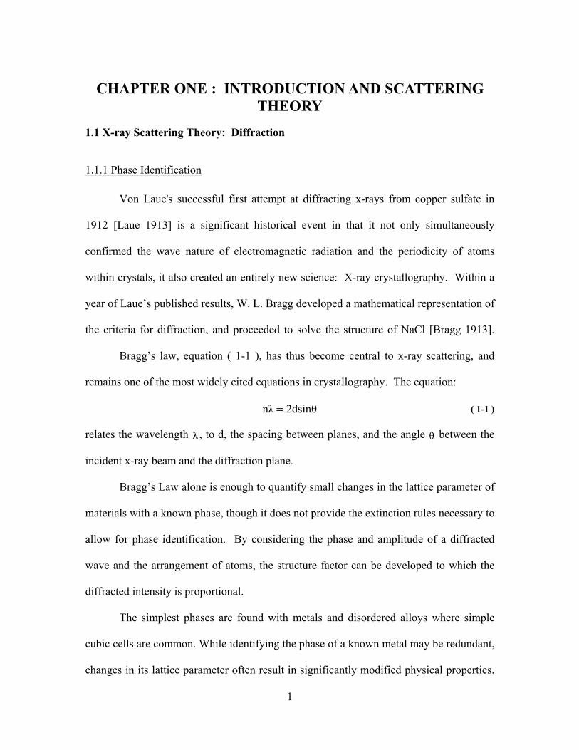
Figure 7 illustrates, by example, the difference between self-affine and self-similar
functions. Figure 7 (a) present the plotted function f(x) = x. Upon rescaling both axis
by equal amount, the same curve is returned (Figure 7 (b)): Self similar behavior is
evident. Figure 7 (c) and (d) present the plotted function f(x) = x1/3. The abscissa in
Figure 7 (c) must be rescaled by a different amount than the ordinate axis if an identical
profile is to be obtained.
19
Figure 7 Self-similar scaling (a and b) and self-affine scaling (c and d)
It should be noted that self-affine scaling is not necessarily valid over all length
scales, but rather only over a relatively narrow spatial window. To elaborate, the shape
of a surface is not well defined over length scales that are smaller than that of an atom,
thereby rendering the self-affine description invalid. Additionally, at very large length
scales, if for example the otherwise self-affine and planar surface is that of a sphere,
different geometrical arguments will be needed to describe the systems large scale
curvature. Nonetheless, since our interest is in the length scales intermediate to these
extremes, the assumption will be made throughout this text that for all length scales being
discussed, the self-affine description of a surface is always valid unless otherwise
specified.
0 10
1
f(x)
x0 3
0
3
3f(x
)
3x
0 10
1
f(x)
x0 27
0
3
3f(x
)
27x
a) b)
c) d)
0 10
1
f(x)
x0 3
0
3
3f(x
)
3x
0 10
1
f(x)
x0 27
0
3
3f(x
)
27x
a) b)
c) d)
20
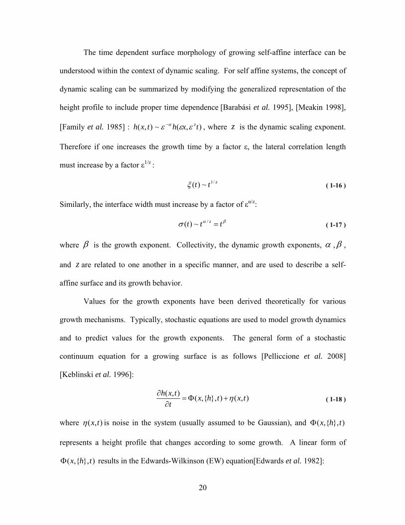
The time dependent surface morphology of growing self-affine interface can be
understood within the context of dynamic scaling. For self affine systems, the concept of
dynamic scaling can be summarized by modifying the generalized representation of the
height profile to include proper time dependence [Barabási et al. 1995], [Meakin 1998],
[Family et al. 1985] : ),(~),( txhtxh z , where z is the dynamic scaling exponent.
Therefore if one increases the growth time by a factor ε, the lateral correlation length
must increase by a factor ε1/z :
ztt /1~)( ( 1-16 )
Similarly, the interface width must increase by a factor of εα/z:
ttt z /~)( ( 1-17 )
where is the growth exponent. Collectivity, the dynamic growth exponents, , ,
and z are related to one another in a specific manner, and are used to describe a self-
affine surface and its growth behavior.
Values for the growth exponents have been derived theoretically for various
growth mechanisms. Typically, stochastic equations are used to model growth dynamics
and to predict values for the growth exponents. The general form of a stochastic
continuum equation for a growing surface is as follows [Pelliccione et al. 2008]
[Keblinski et al. 1996]:
),(),,(),(
txthxt
txh
( 1-18 )
where ),( tx is noise in the system (usually assumed to be Gaussian), and ),,( thx
represents a height profile that changes according to some growth. A linear form of
),,( thx results in the Edwards-Wilkinson (EW) equation[Edwards et al. 1982]:

21
ht
h 2 ( 1-19 )
A quadratic term in ),,( thx yields the Kardar–Parisi–Zhang (KPZ) equation [Kardar
et al. 1986]:
22
2hh
t
h ( 1-20 )
Physically, the EW equation has been used to describe random deposition followed by
instantaneous relaxation [Vvedensky 2003] and predicts the following growth exponent
values:
;2z ;2
2 d
4
2 d
z
( 1-21 )
where d is the dimensionality of the system. The KPZ equation has been physically
attributed to a ballistic deposition process [Aarão Reis 2001] and predicts the following
growth exponent values for systems growing in 1+1 dimensions and 2+1 dimensions
respectively:
;2
3z ;
2
1
3
1
z
( 1-22a )
;58.1z ;38.0 24.0 ( 1-22b )
KPZ scaling further assumes that growth only takes place along the surface normal
thereby predicting conformal growth.
1.2.2 Surface and Interface Kinetics
Figure 8 presents an idealized cross-sectional view of a buried interface between
materials A and B having sinusoidal interface morphology of wavelength,. If material
A is unable to support mechanical stresses (i.e., is a gas, a liquid, or vacuum), then the

22
capillarity driven smoothening of the surface of solid material B (which defines the
interface location) should occur relatively unimpeded. Simply stated; smoothing should
occur due to the diffusion potential being proportional to the local curvature of a surface.
In this case, the atoms of material B are expected to migrate from the crest (position 1B)
towards the trough (position 2B) of the undulating surface, ultimately resulting in a lower
total surface free energy by reduction of the surface area. If material A is a solid and able
to support mechanical stress, then the rates at which the interface between the two
materials may evolve are mechanically coupled.
Figure 8 Idealized solid-solid interface of wavelength λ
For buried interfaces, the local curvature is of opposing sign for each solid, i.e.,
the crest of material A is the trough of material B, and capillarity based smoothing due to
surface diffusion might be expected to occur simultaneously for both of the solid
materials A and B that define the interface. However, if the two solids have very
different interfacial diffusivities, then mechanical stresses will be present, i.e., if material
B has much faster interfacial transport than A, then material A may be considered rigid
and inert and the tendency for atoms of material B to migrate from position 1B to
position 2B will result in a pressure (stress) differential between these two positions
(positive pressure at 2B, negative pressure at 1B) that will modify the diffusion potential

23
for material B so as to inhibit further transport [Larche et al. 1982]. In this case, the
smoothing of the interface will be limited by material A. The mechanical coupling
across the interface between materials A and B can have two possible effects. The first
effect is that the positive pressure induced at position 2B will also result in a positive
pressure at position 2A, such that the pressure differential transmitted across the interface
is of the sign to further enhance the diffusion potential of material A to move from its
crest to its trough (2A to 1A). In this manner the diffusion potential difference driving
transport of each material in the shared interface is coupled mechanically, and an
effective interfacial diffusivity and effective atomic volume for the coupled capillarity
driven interfacial transport of both species can be considered. The second effect is that
the material with the slower interfacial transport may be plastically deformed by the
shared stresses induced by the faster material. This can be expected to be more likely
when one of the materials is in the form of a membrane, having a thickness less than or
comparable to the wavelength of the interfacial roughness.
The introduction of an inhomogeneous and anisotropic strain distribution along
the interface will result in local variations of lattice parameter and a stress contribution to
the chemical potential gradients in the interface that drive atomic transport. This should
limit the effects of capillarity since no longer is interface curvature the only driving force
for diffusion of each species. The effects of strain (lattice parameter) on surface diffusion
have been studied in the past and it has been shown that compressive strains increase the
surface diffusion potential [Brune et al. 1995], though the opposite can at times be true
[Shu et al. 2001].

24
The classical model for capillarity driven smoothing of a solid/vapor interface (or
solid/vacuum interface) by surface diffusion of the solid is well developed [Nichols et al.
1965] [Balluffi et al. 2005] and can be extended to the case of the mechanically coupled
transport of two solids at a buried interface. If the surface is assumed to be homogenous,
isotropic, and sinusoidal, with a time dependent amplitude:
x
tAtxh2
sin)(),( ( 1-23 )
it has been shown that for free surfaces the aforementioned time dependent amplitude
(i.e., 2 the RMS roughness) takes the following form:
tBeAtA4)/2(
0)( ( 1-24 )
Where t is time, λ is wavelength and B is a kinetic coefficient given by kTDB ,
where Ω is the atomic volume of the moving atoms, δ is the interfacial thickness, γ and D
are the interfacial energy and an effective surface diffusivity, respectively, and kT is the
usual product of Boltzmann’s constant and temperature. These results can be extended to
the case of interfacial diffusion along buried interfaces by considering Ω as the effective
average atomic volume of the interfacial materials and D is the effective interfacial
diffusivity of the coupled transport and it is assumed that voids do not form in the
interface.
From equation ( 1-24 ), it can be seen that for a free surface having many different
wavelength components, as is normal for roughness, the short wavelength roughness
should disappear much faster than long wavelength roughness, and thereby cause an
increase in the lateral correlation length. As in a free surface, for a buried interface
25
simple capillarity is expected to not only decrease the total RMS roughness, but also
serve to increase the lateral correlation length of the roughness.
For the case of free surfaces processed such that the height modulations approach
a sinusoidal approximation, the amplitude decay has been experimentally verified [Maiya
et al. 1965] to be proportional to the inverse of wavelength to the fourth power, -4.
Nonetheless, deviations from the -4 dependence have been proposed theoretically
[Dubson et al. 1994] and have been observed experimentally [Castez et al. 2006]
[Erlebacher et al. 2000]. Furthermore, it should be stressed that a -4 dependence is
expected only for surface diffusion. Bulk and vapor diffusion modify the decay exponent
to 3 and 2 respectively.
In regards to encapsulated Cu films, it is expected that will decrease with time
according to equation ( 1-24 ). Furthermore, although and λ are not equivalent, shorter
wavelengths are nonetheless expected to decrease more quickly, leading to an effective
increase in .
1.2.3 X-Ray Reflectivity
X-ray reflectivity is a powerful technique for the study of surfaces and buried
interfaces in thin film systems [Tolan 1998], [Holý et al. 1999]. There are two primary
variations of this technique, specular and diffuse.
In specular X-ray reflectivity, a narrow beam of X-rays is incident upon a
specimen and the intensity of the beam reflected at an angle equal to the incident angle is
measured. The variation of reflected beam intensity as a function of the common
incidence and reflection angle will contain information regarding:

26
Sample density - by determining the critical angle for total external
reflection,
Sample thickness - by measuring the period of the Fresnel oscillations, and
Root-mean-square (RMS) roughness ( 20A )- by measuring the decay
of the reflected intensity.
The second variation is diffuse X-ray reflectivity, in which the intensity of X-rays
scattered at angles not equal to the incidence angle is measured. Analysis of the diffusely
scattered intensity yields information regarding the in-plane structure of the sample, i.e.
the lateral correlation length ( ).
It should be noted that independent values for corresponding to the upper and
lower Cu interfaces may be obtained from the X-ray reflectivity experiments.
Independent values of however, are more difficult to measure; accordingly, the
generalization will be made that the values of represent a combined effect of the upper
and lower film interfaces.
The coherent scattering approximation for evaluation of X-ray reflectivity data
was first developed by Parratt [Parratt 1954]. The effects of roughness were later
described by Vidal [Vidal et al. 1984] and de Boer [De Boer et al. 1996]. The
calculation of the incoherent component of scattered X-rays caused by roughness requires
the use of the distorted-wave Born approximation. For a detailed account of the above,
the reader is directed to references [Holý et al. 1999], [Schmidbauer 2003], [Tolan 1998].
From these, it is known that the intensity of a specular reflection from a rough surface is
attenuated exponentially, and can be described by

27
22
0zQeII ( 1-25 )
Where I0 is the direct beam intensity, Qz is the normal component of the momentum
transfer vector and σ is the RMS roughness. The intensity that is lost from the specular
reflection due to roughness is scattered diffusely in a manner described theoretically;
using the first order Born approximation, the total scattered intensity per unit area for a
single rough surface can be shown to take the following form [Sinha et al. 1988] :
dxdyeeQ
eIQI
yQxQiyxCQz
Q
yxz
z
)(),(2
02
22
)(
( 1-26 )
In this equation C(x,y) is the correlation function (1-14).
The above reflectivity model is applicable to scattering from a single rough
surface (interface). In the case of multiple non-ideal interfaces, the calculation of the
specularly reflected intensity must be further modified by Fresnel coefficients.
Additionally, the correlation function must be modified to include the correlation of each
interface, and their cross correlations. Measurement of the cross correlation allows for a
vertical correlation fraction (or the amount of conformality in topography that translates
from one layer to the next) V to be determined. The model is further complicated by
realizing that equation ( 1-15 ) only has analytical solution for a Hurst exponent equal to
0, ½, or 1 and therefore numeric integration must be used to solve these equations. To
model the experimentally obtained intensity profiles, commercially available software
from Bede is available which employs a genetic algorithm referred to as “Differential
Evolution”[Wormington et al. 1999].

28
CHAPTER TWO : EXPERIMENTAL DETAILS
The works discussed herein focus on metallic thin films on thermally oxidized
single crystal Si substrates. All samples were processed by sputter deposition, and
subsequent x-ray investigations were performed. The varying nature of these distinct
sample sets and the separate investigations undertaken dictates that experimental details
be considered individually as they pertain to each sample set.
2.1 Pt-Ru
To investigate the meta-stable phases of Pt-Ru as a function of composition and
their effects on the alloy work function, several characterization experiments were
performed. The information provided here pertaining to these Pt-Ru investigations has
been previously published [Warren et al. 2008].
2.1.1 Sample preparation
Pt-Ru alloys were prepared by sputter deposition in an ultra high vacuum (UHV)
system. The alloys were formed by co-sputtering Pt and Ru from elemental targets with a
purity of 99.95 %. A quartz crystal thickness monitor was used to calibrate deposition
rates at various DC power settings which allowed for alloy composition to be controlled.
The base pressure was ~ 1 X 10⁻⁸ Torr, while the deposition pressure was maintained at 4
mTorr with a flow of 20 sccm of Ar. The purity of the Ar process gas was maintained by
a hot reactive metal getter. Process gas contamination in the deposition chamber at the
typical deposition pressure of 4 mTorr was confirmed to be less than 10 ppm (the
instrumental sensitivity limit) by closed ion source quadrapole mass spectrometry.

29
Films were deposited onto glass substrates for X-ray diffraction analysis to prevent the
artifacts that often result from multiple scattering events within a single crystal Si
substrate. Films for transmission electron microscopy and work function measurements
were deposited on Si wafer substrates and the details of the work function measurements
have been reported previously [Todi et al. 2006], [Todi et al. 2007].
2.1.2 X-ray Scattering
Because the film thickness is far below the penetration depth of x-rays at normal
incidence, grazing incidence x-ray diffraction (GIXRD) experiments were performed for
the investigation of these Pt-Ru films. A Rigaku D-Max was used with Cu Kα radiation
and a thin films attachment. The GIXRD geometry used in these investigations is
represented schematically in Figure 9.
Figure 9 GIXRD Geometry: i remains constant, the detector scans a range 2θ
In these experiments , the specimen angle remains fixed at low angles, typically
near the critical angle for total external reflection. The sample angle () is equal to the
incident angle (αi). The detector scans its axis across a range Δ2θ. The diffracted beam
therefore makes and angle with the sample αf = (2θ - αi).
Q
2θ
∆2θ
= αi
αf

30
This geometry limits the penetration depth of the x-rays, thereby maximizing
diffraction intensity from the surface layer. It should be noted that, in these grazing
scans, the measured in plane and out of plane components of the scattering vector change
as a function of detector angle; owing to the fact that i remains constant but f does not.
The effect may be quantified by considering the following equations which represent the
in plane and out of plane components of Q; i.e. Qx and Qz respectively:
)cosα(cosα
λ
2πQ ifx
)sinα(sinαλ
2πQ fiz
( 2-1)
Figure 10 presents the path taken through reciprocal space of a GIXRD
experiment in which αi is taken to be 5° and λ=1.54Å. Because Qx and Qz both vary
comparably in GIXRD, highly textured or epitaxial films may not be measurable. This
scattering geometry is however very well suited for poly crystalline thin films. Though
not discussed here, structural depth profiles may additionally be generated using this
technique by performing several GIXRD measurements in which αi is incremented
between subsequent scans.

31
Figure 10 GIXRD trace through reciprocal space
GIXRD was used to investigate the crystal structure of Pt-Ru alloys as a function
of their respective compositions. Analysis of GIXRD patterns was performed using
commercially available software frm MDI: Jade 7.5. The Pt-Ru thin films, on glass
substrates, were cut into approximately 1x1cm squares and were rinsed with alcohol to
provide a relatively clean surface prior to characterization.
Additionally X-ray reflectivity (XRR) was used to determine film thickness by
analysing secular reflectivity patterns with Bede REFS software [Wormington et al.
1999]. Only specular scans were collected for the purpose of thickness measurement; A
detailed discussion of x-ray reflectivity is presented in subsequent sections, pertaining to
the investigation of encapsulated metallic thin films.
0 -1 -2 -3 -4 -50
1
2
3
4
5
Qz [
Å-1]
Qx [Å-1]
32
2.1.3 Additional Characterization
Rutherford backscattering spectroscopy (RBS), performed with a General IONIX
1.7 MV Tandetron RBS system, was used to determine alloy composition. RBS data was
analyzed using the free software package RUMP.
To supplement x-ray analysis, plan-view bright field and dark field images were collected
along with corresponding selected area electron diffraction patterns. A Phillips Tecnai
F30 transmission electron microscope was used. Samples were prepared using a back
etch technique to remove the Si substrate [Yao et al. 2008].
2.2 Encapsulated Cu and W
A series of encapsulated Cu and W thin films were extensively characterized by
X-ray and transmission electron microscopy (TEM) methods. The original motivation
for establishing deposition processes for these specimens was to study the electronic
properties of the encapsulated nanometric metallic films, and many details regarding
sample preparation may be found in previously published works; references to which are
provided in the following section.
2.2.1 Sample preparation
Details of the sample preparation process have previously been published [Sun et
al. 2010], [Choi et al. 2012]. Furthermore, the electronic properties of these films were
the focus of past dissertations by Sun [Sun 2009] and Choi [Choi 2011]:
The following is an excerpt from the work by Sun:
“The encapsulated Cu thin films were prepared on 3” diameter Si
(100) substrates having a nominally 1500Å thick layer of thermally grown

33
SiO2. The substrates were mounted onto a Cu substrate platen with a
mechanical clamp ring and a thin layer of vacuum grease (Apeizon N)
between the wafer backside and the platen to insure adequate thermal
contact in vacuum. The Cu substrate platen was introduced into a UHV
sputter deposition chamber via a load-lock chamber and RF sputter
cleaned in 10 mTorr of Ar+2%O2 for 15 minutes at low power (0.2
W/cm²). After cleaning, the substrate and platen were cooled prior to
deposition to -40°C by contact with a liquid nitrogen cooled Cu plate. The
substrate temperature prior to deposition was controlled by variation of the
allowed cooling time and was confirmed for each sample by measurement
of plate temperature immediately upon venting.
For films having the SiO2/Ta/Cu/Ta/SiO2 structure, a layer of 20Å of Ta
was DC sputter deposited immediately prior to, and again after, the Cu
layer deposition. These films were otherwise prepared similarly to the
SiO2/Cu/SiO2 process described above. The Cu films, of thickness ranging
from 270Å to 1580Å, were deposited by DC sputter deposition from high
purity (99.9999%) Cu targets at a rate of 6 Å/sec onto the electrically
grounded substrates.
layer depositions were performed at a total pressure of 4 mTorr of Ar
process gas while the metal layers were deposited at 2 mTorr of
Ar+3%H2. A deposition chamber pressure in the 10-9 Torr range was
obtained prior to film deposition and the nominally 99.999% purity Ar

34
was passed through a hot reactive metal getter purifier (SAES Pure Gas)
prior to introduction to the chamber.
Annealing treatments of 150°C and 600°C for 30 minutes were
performed on both SiO2/Cu/SiO2 and SiO2/Ta/Cu/Ta/SiO2 structure
samples in a tube furnace to provide grain size variations at each thickness
of the Cu layer. An Ar+5%H2 reducing process gas was used in both
annealing treatments to prevent oxidation of the Cu layer.”
The Encapsulated W films were deposited using the same procedure as that is
described by Sun, with the modification that depositions were performed at room
temperature and no RF substrate cleaning was used. [Choi 2011].
2.2.2 X-ray Scattering
2.2.2.1 X-ray Diffraction
X-ray scattering investigation of encapsulated Cu and W films were performed
using a grazing incidence diffraction (GID) geometry. The large lateral coherence,
established by the in plane scattering geometry, renders GID experiments well suited for
studying the in plane structure of crystalline matter. Detailed descriptions of in plane
scattering experiments and scans through reciprocal space may be found in textbooks
[Birkholz et al. 2006], [Holý et al. 1999].
Figure 11 illustrates GID schematically. I0 and If indicate the incident and
diffracted beams respectively. The angles between the respective beams and the sample
plane are denoted as αi and αf (which in these experiments are equal to each other) and

35
together dictate the in plane and out of plane components of Q, the scatting vector. 2θ is
the scattering angle; the samples angle (, not shown) equals half of 2θ.
Figure 11 GID Geometry: i and f are small and equal, and approximately equal to . Q remains in the plane.
Because I0 emits from a fixed source, the sample tilt angle, , establishes αi and
αf. A GID experiments may therefore be performed by moving to low angles (~2°),
and proceeding with a coupled θ-2θ scan. The in plane and out of plane components of Q
may therefore be written as follows:
sinθcosαsinθcosαλ
2πQ ifx
fiz sinαsinαλ
2πQ
( 2-2 )
While values for α may be taken to equal , close inspection reveals that αi and
αf are however only approximately equal to , and are additionally functions of .
Figure 12 illustrates the co-dependence of α on and . Depictions of at 0° and 90°
are provided at three -tilts: 90° (Figure 12(a)), 5° (Figure 12(b)) and 0° (Figure 12(c)) .
In all cases αi only equals when is at 90°. At =0°, αi is 0°, irrespective of .
n
I0
D αi
2θ
If
αf Q

36
Figure 12 Dependence of αi on and
By inspection of Figure 12, the following conjecture for determining αi may be
deduced:
sinψωsinsinα 1i
( 2-3 )
For the encapsulated Cu and W films discussed here, reciprocal space scans were
performed such that Qz remained constant and minimized, while Qx spanned the range
=0°
=90°
=90°
i=90°i=0° =90°
a)
=0° =90°
=5° i=5°
i=0° =5°
b)
=0° =90°
=0° i=0°=0°i=0°
c)

37
inclusive of all major Bragg reflections. Figure 13 presents the path taken through
reciprocal space of a GID experiment calculated from equation ( 2-2 ) and ( 2-3 ), where
λ=1.54Å.
Figure 13 GID trace through reciprocal space with constant αi
A synchrotron source is ideal for GID experiments owing to its high spectral
purity and high intensity. Accordingly, all diffraction experiments on encapsulated Cu
and W thin films were performed at the Stanford Synchrotron Radiation Lightsource
(SSRL). Data were collected on beam line 7–2. This beam line is equipped with a Huber
6+2 -circle diffractometer, and a He filled sample stage to decrease the air scattering
0 2 4 60.00
0.25
Qz [
Å-1]
Qx [Å-1]

38
background. X-rays with a wavelength of 1.54 Å were monochromated with a double
bounce Si(111) crystal.
2.2.2.2 X-ray Reflectivity
All X-ray reflectivity (XRR) experiments were also performed at SSRL. Data
were collected on thin-film diffraction beam line 2–1. This beam line is equipped with a
Huber 2-circle goniometer, a pair of 1 mm slits as the analyzer, and a He filled sample
stage to decrease the air scattering background. X-rays with a wavelength of 1.549 Å
were monochromated with a double bounce Si(111) crystal. Three types of scans were
performed in order to study the (top and bottom) interfacial roughness and its lateral
correlation length. To determine film thickness and RMS roughness (of top and bottom
Cu interfaces), specular and offspecular scans were collected: for specular scans ω=2θ/2=
θ, whereas for off specular scans ω=2θ/2 ±0.15°. The offspecular scans were used to
subtract the contribution of diffusely scattered X-rays to the specular reflection, resulting
in a purely specular reflectivity pattern. Data were collected for 2θ values ranging
between 0.2° to 12°, with a step size of 0.02°, 0.01°, or 0.005°, depending on film
thickness. To determine the lateral correlation length, rocking curves were collected by
fixing the detector at approximately 3° of 2θ, and rocking the sample through ±1.5° of ω.
A 2θ of 3° was chosen to obtain diffuse scattering that was sufficiently strong. The in
plane component of the scattering vector was later determined by realizing that
Qx=(4π/λ)sinθcosθ, and was subsequently modeled to determine the lateral correlation
length of roughness. The X-ray data was analyzed using Bede REFS software
[Wormington et al. 1999]. Specular reflectivity profiles are modeled by inputting
thickness, density and roughness values into REFS; necessary instrument parameters,

39
such as silt settings and X-ray wavelength, are also inputted. A fitting routine is
subsequently executed. The measured values for thickness, density, and roughness are
then used to model each corresponding diffuse reflectivity profile, which then only
depends on vertical correlation length, vertical correlation fraction, and the fractal
exponent.
2.2.3 Additional Characterization
The microstructure of these films were extensively studied by TEM; details have
been published elsewhere [Sun 2009], [Choi 2011]. The following represents a summary:
The TEM samples were prepared using a back-etching technique [Yao et al.
2008] and examined by a combination of techniques. High angle annular dark field
(HAADF) imaging in scanning TEM mode was used at relatively low magnifications to
assess the void fraction present in the film. In the case of Cu films, Hollow cone dark
field (HCDF) TEM imaging was used to provide high diffraction contrast for grain size
measurements which were based on a hand tracing method [Sun 2009]. In the case of W
films, an Automated Crystallography in the TEM (ACT) technique was employed.
Details of the ACT technique may be found in the Doctoral Dissertation of Dooho Choi
[Choi 2011]. The reported grain size is the diameter of the equivalent circle with area
equal to the average of the grain areas and the errors on the mean are quoted as 2σ values
at a 95% confidence level for the given grain population. For samples in Table 14 (c) the
reported grain size is an approximation based on resistivity data and film thicknesses
measured by specular XRR. This was made possible by previously published works
which provide quantitative verification of the Myadas-Schotzkey model of resistivity
[Sun et al. 2008], [Sun et al. 2009], [Sun et al. 2010]. The specimens whose grain size

40
was calculated based on resistivity are only included in x-ray reflectivity discussions
pertaining to scaling dynamics.
2.3 GlobalFoundries W
2.3.1 Sample Preparation
Three W thin films specimens were processes by industrial partners at
GlobalFoundries. These were deposited onto thermally oxidized Si substrates via
chemical vapor deposition. Table 2 lists all processing details made available.
Table 2 GlobalFoundries W processing details ID SiO2
[Å]WNucleation
[Å]WCoolfill[Å]
WCVD[Å]
WTotal[Å]
GFW2 1000 23 111 0 134
GFW4 1000 23 0 106 129
GFW5 1000 23 29 75 127
2.3.2 X-ray Scattering
X-ray scattering investigations of W films from GlobalFoundries were performed
using a grazing incidence diffraction (GID) geometry, similar to that described in section
2.2.2.1 X-ray Diffraction. In these experiments, the specimen was held at a constant
inclination angle, =2°: Real space, θ-2θ, scans were performed so as to include all
major Bragg reflections. Because was held constant, αi and αf varied during the
diffraction experiment; thereby resulting in a small change in Qz . Figure 14 presents the
path taken through reciprocal space of the GID experiment described here. Equation
( 2-2 ) and ( 2-3 ) were used to generate the trace, where λ=1.54Å and =2°. The change
in Qz is however small, and ultimately experimentally negligible: No corrections are
made to the experimentally obtained diffraction profiles to accommodate the non-
constant Qz.
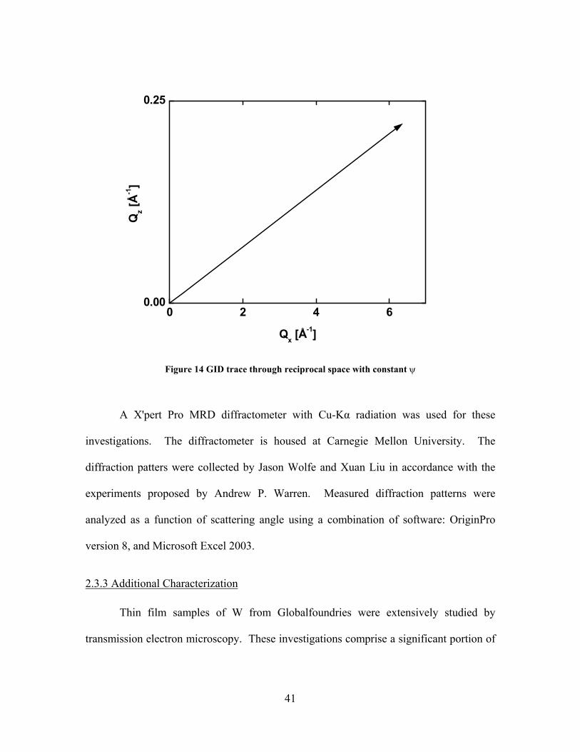
41
Figure 14 GID trace through reciprocal space with constant
A X'pert Pro MRD diffractometer with Cu-Kα radiation was used for these
investigations. The diffractometer is housed at Carnegie Mellon University. The
diffraction patters were collected by Jason Wolfe and Xuan Liu in accordance with the
experiments proposed by Andrew P. Warren. Measured diffraction patterns were
analyzed as a function of scattering angle using a combination of software: OriginPro
version 8, and Microsoft Excel 2003.
2.3.3 Additional Characterization
Thin film samples of W from Globalfoundries were extensively studied by
transmission electron microscopy. These investigations comprise a significant portion of
0 2 4 60.00
0.25
Qz [
Å-1]
Qx [Å-1]

42
Xuan Liu's doctoral dissertation; a student at Carnegie Mellon University, Pittsburg, PA
(Advisor: Katayun Barmak).
Plan view electron transparent samples for TEM investigations were prepared by
a back etch method [Yao et al. 2008]. Subsequent TEM analysis was preformed on a FEI
Techni F20. Orientation maps were generated using a commercially available software
package from NanoMEGAS: ASTARTM, and analyzed using the TSLOIMTM

43
CHAPTER THREE : METASTABLE PHASE IDENTIFICATION
The continued scaling of device dimensions in complementary metal-oxide-
semiconductor (CMOS) technology in the sub 700Å region requires an alternative high
dielectric (high-κ) oxide layer to counter tunneling leakage currents, and a metallic gate
electrode to address limitations of polysilicon [Wilk et al. 2001]. A key parameter for the
choice of the metal gate material is its work function. For p-channel MOS (p-MOS), Pt
and Ru are both possible choices due to their higher work function value. Alloys of these
metals can also be considered to achieve an optimized or “tunable” work function. A
detailed study of the resulting phases for a binary metal alloy system is important, as it
can be expected to impact the important properties of the gate electrode material, such as
its work function, electrical resistivity and thermal stability. For FCC materials, the
dependence of work function and lattice parameters on alloy composition has been
demonstrated theoretically and corroborated experimentally [Abrikosov et al. 1993]. In
this section, a detailed phase characterization of Pt-Ru binary alloy thin films performed
predominantly by grazing incidence x-ray diffraction (GIXRD) is reported.
3.1 Objectives
The objective of this research is to gain insight into compositional dependence of
crystallographic structure in Pt-Ru alloy thin films, and to understand its effect on the
alloy's electronic work function. This work additionally illustrates the continued
relevance of x-ray diffraction for phase identification of simple binary alloy systems

44
3.2 Results
The structural dependence on composition can be seen in the GIXRD patterns and
is qualitatively confirmed with electron diffraction. Figure 15 shows grazing incidence
GIXRD of thin films spanning the compositional range from pure Pt to pure Ru where
the intensities for each scan have been offset for clarity.
The pure Pt and pure Ru samples are clearly single phase FCC and HCP,
respectively, and what is of interest is the transition from FCC to HCP that occurs at
intermediate compositions. The lower angle reflections shown in Figure 15(a) reveal an
FCC(111) peak for pure Pt that gradually shifts to higher angles and can ultimately be
indexed as the HCP(002) peak in pure Ru. As this peak is common to both crystal
structures, it cannot be used as evidence of the absence of either one of these two phases.
However, the FCC(200) peak is unique to the FCC phase and it is observed to decrease in
intensity with increasing Ru concentration and is not discernable in Figure 15(a) at
compositions above 43 at% Ru. This observation is accompanied by the growth of the
HCP(100) and (101) peaks with increasing Ru concentration. Both of these peaks are
clearly present in the sample having 63 at. % Ru, and some indication of the HCP(101)
peak is also present at 58 at. % Ru. The higher angle XRD peaks for these same samples
(Figure 15(b)) clearly show the presence of the HCP phase at 58 at. % Ru, as the (103)
peak is unique to the HCP phase. The HCP(103) peak intensity increases as the Ru
concentration is increased. Also evident is the shift to higher angles of the FCC(331),
and its splitting into HCP(112) and (201). Clearly, the 58 at. % Ru sample is at or near
the transition with composition from FCC phase to HCP phase and warrants a more
detailed examination.
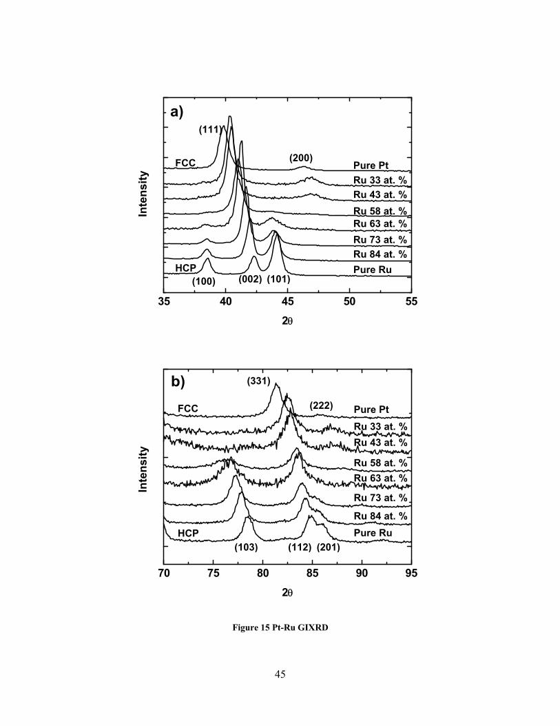
45
Figure 15 Pt-Ru GIXRD
35 40 45 50 55
Inte
nsi
ty
2
Ru 33 at. %
Pure Pt
Pure Ru
Ru 43 at. %
Ru 58 at. % Ru 63 at. %
Ru 73 at. %
Ru 84 at. %
FCC
HCP (100) (101)(002)
(111)
(200)
a)
70 75 80 85 90 95
Inte
nsi
ty
2
Ru 33 at. %
Pure Pt
Pure Ru
Ru 43 at. %
Ru 58 at. %
Ru 63 at. %
Ru 73 at. %
Ru 84 at. %
FCC
HCP (103) (112) (201)
(331)
(222)
b)
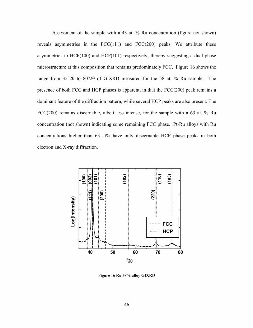
46
Assessment of the sample with a 43 at. % Ru concentration (figure not shown)
reveals asymmetries in the FCC(111) and FCC(200) peaks. We attribute these
asymmetries to HCP(100) and HCP(101) respectively; thereby suggesting a dual phase
microstructure at this composition that remains predominately FCC. Figure 16 shows the
range from 35°2θ to 80°2θ of GIXRD measured for the 58 at. % Ru sample. The
presence of both FCC and HCP phases is apparent, in that the FCC(200) peak remains a
dominant feature of the diffraction pattern, while several HCP peaks are also present. The
FCC(200) remains discernable, albeit less intense, for the sample with a 63 at. % Ru
concentration (not shown) indicating some remaining FCC phase. Pt-Ru alloys with Ru
concentrations higher than 63 at% have only discernable HCP phase peaks in both
electron and X-ray diffraction.
Figure 16 Ru 58% alloy GIXRD
FCC
HCP
40 50 60 70 80
(220
)
(200
)
(111
)
(103
)
(110
)
(102
)
(101
)(0
02)
Lo
g(I
nte
nsi
ty)
o2
(100
)
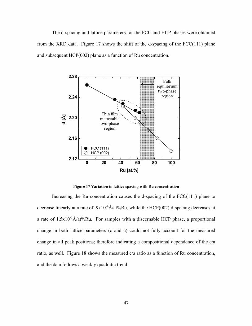
47
The d-spacing and lattice parameters for the FCC and HCP phases were obtained
from the XRD data. Figure 17 shows the shift of the d-spacing of the FCC(111) plane
and subsequent HCP(002) plane as a function of Ru concentration.
Figure 17 Variation in lattice spacing with Ru concentration
Increasing the Ru concentration causes the d-spacing of the FCC(111) plane to
decrease linearly at a rate of 9x10⁻⁴Å/at%Ru, while the HCP(002) d-spacing decreases at
a rate of 1.5x10⁻³Å/at%Ru. For samples with a discernable HCP phase, a proportional
change in both lattice parameters (c and a) could not fully account for the measured
change in all peak positions; therefore indicating a compositional dependence of the c/a
ratio, as well. Figure 18 shows the measured c/a ratio as a function of Ru concentration,
and the data follows a weakly quadratic trend.
0 20 40 60 80 1002.12
2.16
2.20
2.24
2.28
d [
Å]
Ru [at.%]
FCC (111) HCP (002)
Bulkequilibriumtwo‐phaseregion
Thinfilmmetastabletwo‐phaseregion

48
40 60 80 100
1.58
1.60
1.62
1.64
c/a
Ru [at%]
Figure 18 Effect of composition on c/a ratio in HCP Pt-Ru films
Figure 19 presents the results of measurements of the work function for these
alloys as a function of composition, and a complex, non-linear, behavior is evident. The
variation in work function follows the observed metastable extension of the HCP phase
identified by GIXRD (Figure 17). Regions of weak compositional dependence are
observed in the single-phase and near single-phase regions of the alloy thin films; marked
as region A in Figure 19.

49
Figure 19 Nonlinear work-function response to Ru concentration
Steep compositional dependence is observed across the intermediate compositional range
where the c/a ratio is observed to decrease most rapidly as Ru concentration is increased.
(Figure 19, region B). The work function asymptotes to that of pure Ru as the
concentration of Pt approaches 0 Figure 19, region C). Figure 20 shows the strong
correlation between the electronic work function and c/a ratio of the HCP phase samples,
where a linear relationship is observed.
0 20 40 60 80 1004.8
4.9
5.0
5.1
5.2
Wo
rk F
un
ctio
n [
eV]
Ru [at.%]
Thinfilmmetastabletwo‐phaseregion
A
B
C

50
Figure 20 Dependence of Pt-Ru Work Function on c/a ratio of HCP phase
According to the equilibrium phase diagram for bulk Pt-Ru alloys [Massalski et
al. 1990] , a Ru content of less than 62 at. % is expected to consist of only FCC phase,
and Ru concentrations of more than 80 at. % are expected to be HCP. Both FCC and
HCP phases of Pt and Ru are expected to be present for Ru concentrations between 62
and 80 at.%. However, structural analysis of the Pt-Ru thin film alloy system reveals a
notable increase in the compositional range of the hexagonal close packed (HCP) phase,
suggesting a metastable extension of the HCP phase stability as compared to bulk Pt-Ru
alloys. A similar meta stable extension had been noted in RF sputtered electrodes studied
in a GID geometry [Kim et al. 2005]. In the case of the thin films discussed herein, a
mixed HCP-FCC phase becomes apparent with Ru concentrations as low as 43 at%.
Furthermore, the FCC phase is completely absent (single phase HCP) for Ru
Pure Ru
Ru 58at%
1.58 1.60 1.62 1.644.8
4.9
5.0
5.1
Wor
k F
unct
ion
[eV
]
c/a

51
concentrations higher than approximately 65 at.%. In addition to the metastable
extension of the HCP phase, a gradual change of phase is apparent in the form of a
linearly decreasing d-space of the FCC(111), and subsequent HCP(002) planes, as the
Ru concentration is increased. A decrease in c/a ratio is also evident in the HCP phase.
3.3 Conclusion
Pt-Ru alloy thin films were sputter deposited in an ultra- high vacuum chamber by
dc magnetron sputtering and were extensively characterized by GIXRD to quantify the
phase dependence of the alloy composition in the Pt-Ru alloy thin films. The equilibrium
binary phase diagram [Massalski et al. 1990] for bulk Pt–Ru alloys indicate a two-phase
microstructure for compositions from 62 to 80 at.% Ru. However, for these thin films a
notable increase in the compositional range of the HCP phase was observed, suggesting a
metastable extension of the HCP phase stability as compared to bulk Pt-Ru alloys. The
steepest change in the electronic work function for the intermediate alloy compositions
coincided with a rapid change in the c/a ratio of the HCP phase.

52
CHAPTER FOUR : GRAIN SIZE AND DEFECT ANALYSIS
X-ray line profile analysis has been used to investigate the grain size and
microstructure of Cu and W thin films. Two distinct sets of W films will be discussed;
those referred to as GlobalFoundries W (or GF-W) will be discussed separately at the end
of this chapter, and are the only specimens investigated using a conventional
diffractometer; all other experiments were performed using a synchrotron source.
Examples of normalized x-ray line profiles (circles) measured at SSRL, and their
corresponding fits (solid line) are provided in Figure 21. Figure 21(a) shows an example
Grazing Incidence Diffraction (GID) of a Cu film with a thickness of 1439Å and an in
plane grain size (as measured by hollow cone dark field TEM methods) of 2480Å. This
data corresponds to sample Cu-08 in Table 3, which summarizes the results of the peak
fitting. Figure 21(b) shows an in-plane scan of a W film with a thickness of 189Å and an
in plane TEM grain size of 1020Å. This data corresponds to sample W-01 in Table 3.
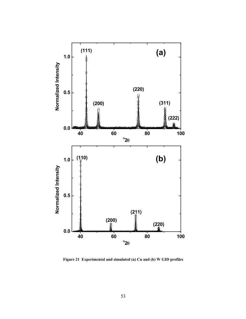
53
Figure 21 Experimental and simulated (a) Cu and (b) W GID profiles
40 60 80 1000.0
0.5
1.0
(222)
(311)
(220)
(200)
No
rmal
ized
In
ten
sity
o2
(111)
40 60 80 1000.0
0.5
1.0
(220)
(211)
(200)
No
rmal
ized
In
ten
sity
o2
(110)
(a)
(b)

54
The table includes measured values, in real space coordinates, of peak positions
(2θ) and FWHM(Δ(2θ)) and the subscripts indicate the hkl values for each peak. Printed
values of FWHM have not been corrected for instrumental broadening. As discussed
previously, instrument effects may generally be neglected for these samples.
Nevertheless, corrections for instrumental broadening, based on Figure 1, have been
made in analysis of peak profiles for grain size, whose results will be presented in
subsequent tables and figures.
The x-ray wavelength (λ), film thickness (TXRR) and TEM-based values of grain
size (DTEM) are also included in Table 3. Thickness values were obtained through x-ray
reflectively analysis, which is discussed extensively in chapter 4 which specifically
includes samples Cu-01, Cu-02, Cu-05, and Cu-07.
Because the specimens discussed in the this section have comprised significant
portions of works published elsewhere, Table 4 presents a list of alternative specimen
identifications which may be used for cross correlations. This table should also be used
as reference for any subsequent works which may be based on these sample sets.

55
Table 3 Cu and W Peak Fitting Results
IDTXRR[Å]
DTEM[Å]
λ[Å]
Δ(2Θ)111[°2Θ]
2Θ111[°2Θ]
Δ(2Θ)200[°2Θ]
2Θ200 [°2Θ]
Δ(2Θ)220[°2Θ]
2Θ220[°2Θ]
Δ(2Θ)331[°2Θ]
2Θ311[°2Θ]
Δ(2Θ)222[°2Θ]
2Θ222[°2Θ]
Cu‐01 270 405 0.200 43.604 0.530 50.842 0.346 74.739 0.444 90.757 0.422 95.996Cu‐02 336 684 0.182 43.466 0.423 50.556 0.361 74.494 0.512 90.333 0.438 95.614Cu‐03 371 648 0.180 43.586 0.433 50.829 0.307 74.677 0.412 90.691 0.349 95.930Cu‐04 417 877 0.134 43.526 0.353 50.673 0.251 74.539 0.326 90.493 0.290 95.756Cu‐05 451 1011 0.121 43.552 0.335 50.696 0.167 74.580 0.237 90.549 0.223 95.821Cu‐06 836 2215 0.093 43.527 0.234 50.662 0.184 74.537 0.275 90.473 0.255 95.782Cu‐07 1439 2480
1.549358
0.071 43.567 0.258 50.814 0.119 74.645 0.375 90.679 0.164 95.896
IDTXRR[Å]
DTEM[Å]
λ[Å]
Δ(2Θ)110 [°2Θ]
2Θ110[°2Θ]
Δ(2Θ)200[°2Θ]
2Θ200 [°2Θ]
Δ(2Θ)211[°2Θ]
2Θ211[°2Θ]
Δ(2Θ)220[°2Θ]
2Θ220[°2Θ]
W‐01 189 1020 0.125 40.203 0.112 58.208 0.185 73.101 0.220 86.882 W‐02 283 1060 0.128 40.198 0.164 58.211 0.200 73.096 0.256 86.885 W‐03 425 1010 0.140 40.247 0.194 58.278 0.232 73.191 0.287 87.002 W‐04 607 1110 0.134 40.285 0.189 58.324 0.216 73.270 0.266 87.104
W‐05 1229 1090
1.540178
0.124 40.271 0.183 58.330 0.200 73.263 0.243 87.095

56
Table 4 Alternative Sample ID's ID AlternativeID
Cu‐01 ‐‐ ‐‐ N43_101006d_150Cu‐02 ‐‐ ‐‐ N43_101006d_600Cu‐03 ‐‐ ‐‐ N35_072106a_150Cu‐04 ‐‐ ‐‐ N35_072106a_400Cu‐05 ‐‐ ‐‐ N50_071606B_150Cu‐06 ‐‐ ‐‐ N50_071606B_400Cu‐07 ‐‐ ‐‐ N35_101006e_150‐‐ W3N5 B5 1100
‐‐ W3N10 B10 1099
W‐01 W3N20 B20 1087
W‐02 W3N30 B30 1092
W‐03 W3N40 B40 1091
W‐04 W3N60 B60 1090
W‐05 W3N120 B120 1089
W‐06 W3N180 B180 1088
4.1 Objectives
The objective of this research is to examine the utility of conventional x-ray peak
profile analysis methods for the determination of grain size and microstrain in metallic
thin film specimens. Results are compared to TEM based investigations.
4.2 Results of Scherrer Analysis
The Scherrer method is the simplest method of line profile analysis. It is
generally understood to provide only an approximation of crystallite size, owing mainly
to the fact that it fails to account for strain broadening. Nevertheless, the method is still
widely used and provides many insights into the microstructure of a system. Results of
Scherrer analysis are presented in Table 5. Scherrer grain sizes were obtained using
equation ( 1-6 ) and values from Table 3 after correcting for instrument broadening as per
equation ( 1-2 ) and Figure 1 (solid line). For every sample, two Scherrer grain sizes are
reported: These values represent grain sizes obtained with and without empirical shape

57
factor optimization (discussed in following section). XRR based thickness values and
TEM based grain size values are included for reference.

58
Table 5 Results of Scherrer Analysis
IDTXRR[Å]
DTEM[Å]
DS(K=1.00)[Å]
DS(K=1.55)[Å]
Cu‐01 270 405 480 745Cu‐02 336 684 528 819Cu‐03 371 648 534 828Cu‐04 417 877 721 1118Cu‐05 451 1011 801 1242Cu‐06 836 2215 1052 1631Cu‐07 1439 2480 1403 2175W‐01 189 1020 759 1176W‐02 283 1060 741 1148W‐03 425 1010 676 1048W‐04 607 1110 707 1096W‐05 1229 1090 765 1186W‐06 1801 1160 778 1206
4.2.1 Grain Size
Scherrer analysis was performed on the first order reflection with maximum
intensity; i.e. the (111) for FCC Cu and the (110) for BCC W. A shape factor (k=1) was
assumed. The maximum grain size that was found to be reliably measurable is herein
reported to be on the order of 1200Å. Such a resolution limit is common, and its source
is typically attributed to instrumentation. It is reported that when the average TEM based
grain size approaches 2000Å, Scherrer analysis yields squared errors that are one hundred
times higher than that for 1200Å grained specimens. Specifically, Scherrer-based
analysis yields squared errors on the order of 104 for grains up to approximately 1200Å;
These errors increase to an order of 106 for larger grained specimens.
Recall however, that a synchrotron source was implemented for these
experiments, so as to render the contribution of instrument broadening negligible.

59
Indeed, based on the measured instrument resolution, (0.02°2θ at 43°2θ), a grain size of
nearly 0.5μm should be quantifiable. Instrumental broadening therefore cannot be
confirmed to be the source of the observed 1200Å grain size limit.
The data and hypothetical perfect correspondence to TEM based values are
plotted in Figure 22 where filled and half-filled circles represent Cu and W films
respectively. Open circles represent (Cu) outliers whose x-ray based measures of grain
size significantly deviate from expected values. A total sum of the errors squared of
3.3106 is reported for the data plotted in Figure 22.
0 1000 2000 30000
1000
2000
3000
Cu W Outliers
DS [
Å]
DTEM
[Å]
Figure 22 Scherrer and TEM Grain Size Comparison
4.2.2 Shape Factor
Having the unprecedented grain size analysis obtained through exhaustive TEM
studies, the Scherrer equation has been used to experimentally evaluate the shape factor

60
for Cu and W thin films measured in-plane. Regression methods were used to minimize
the sum squared error between TEM and Scherrer grain size values. Using this approach,
a shape factor (k) equal to 1.55 was found to provide the best correlation between TEM
and XRD results.
Typical values for the shape factor are 0.88 (when the peak integral breath is used
in analysis), 0.94 (when the peak full-width at half-maximum is used in analysis) or 1
(reasonable approximation) [Warren 1990]. More rigorously obtained values were
published by Langford and Wilson [Langford et al. 1978]. Langford and Wilson present
k values that depend on crystallite shape and hkl. The authors contend that "crystallites
are usually irregular in shape, but on average they maybe regarded as having a regular
external form." They continue "If the crystallites making up the specimen have a
reasonably well defined shape, and if this shape has a reasonably well defined relation to
the crystal axis, the numerical value of the Scherrer constant will depend on the index of
reflection."
For (110) (BCC W specimens) and (111) (FCC Cu specimens) reflections
specifically, whose full-width at half-maximum is used for analysis, shape factor values
ranging between 0.83 and 0.95 are expected according to Langford and Wilson.
Similarly, shape factors for platelets have been reported as 0.886 [Smilgies 2009]. The
experimentally obtained value however is 1.55. Limited data prevents an assessment of a
dependence on reflection index. However, a global value of 1.55, applied to Scherrer
analysis of both Cu and W thin films, presents a significant improvement in grain size
results when compared to TEM based measurement. Figure 23 shows TEM grain sizes
plotted against that obtained through Scherrer analysis. The solid line represents a

61
hypothetical perfect correspondence for reference. By inspection, X-ray based grain
sizes analyzed using a shape factor of 1.55 lie more closely along the solid line than do
grain sizes analyzed with a shape factor of 1.00. To quantify; using k=1.00 provides a
sum squared error of 3.3106. Using k=1.55 however, reduces the sum squared error to
7.6105.
0 1000 2000 30000
1000
2000
3000
(Cu) (W): k = 1.55(Cu) (W): k = 1.00
DS [
Å]
DTEM
[Å]
Figure 23 Optimized Scherrer shape factor showing improved agreement between GID and TEM
grain size values.
The fact that the experimentally determined shape factor exceeds the anticipated
value may be attributed to the highly irregular crystallite shape. From plan view TEM
micrographs it is apparent that the crystallites do not have a well defined shape, and no
obvious correlation exists between crystallite shape and crystallographic orientation To

62
highlight this point Figure 24(a) shows a hollow cone dark field (HCDF) image of sample
Cu-03, and Figure 24(b) shows a bright field (BF) image of W-01. Additionally,
Scherer's analysis assumes that the only mechanism responsible for peak broadening is
grain size. Therefore stain-related broadening effects are folded into the shape factor;
rendering it more aptly referred to as a "scaling factor."

63
Figure 24 (a) Cu-03 HCDF, (b) W-01 BF
4.3 Results of Williamson-Hall Analysis
To further investigate x-ray peak profile broadening, the Classical and Modified
Williamson-Hall methods were employed. Because significant micro-strains (variance in
lattice spacing) are well known to contribute to peak broadening, analytical methods that
are strain-sensitive may provide measures of grain size that more closely match that
obtained by direct TEM studies. In the event that more reliable grain size values are not
obtained by these more sophisticated methods, it is shown that non-negligible, yet under-
researched, strains induced by interface phenomena, do indeed contribute to peak
broadening. The results of Williamson-Hall (W-H) and modified Williamson-Hall
(ModW-H) analysis are summarized in Table 6. Tabulated values include classical
Williamson-Hall grain sizes (DW-H) modified Williamson-Hall grain sizes (DM), and
micro-strain, i.e., the slope of the Williamson-Hall plot (WH) and modified Williamson-

64
Hall plot (M). XRR based thickness and TEM based grain size values are again included
for reference.
Table 6 Results of Williamson-Hall analysis
IDTXRR[Å]
DTEM[Å]
DW‐H[Å] WH
DM[Å] M
Cu‐01 270 405 987 2.2E‐03 727 5.4E‐03
Cu‐02 336 684 1990 2.9E‐03 1368 8.1E‐03
Cu‐03 371 648 872 1.5E‐03 901 5.1E‐03
Cu‐04 417 877 1598 1.6E‐03 1282 4.4E‐03
Cu‐05 451 1011 1148 7.9E‐04 1100 2.1E‐03
Cu‐06 836 2215 ‐‐ 1.9E‐03 3077 4.5E‐03
Cu‐07 1439 2480 3729 9.3E‐02 2816 2.4E‐03
W‐01 189 1020 1140 9.9E‐04 1390 2.8E‐03
W‐02 283 1060 1566 1.6E‐03 1631 4.2E‐03
W‐03 425 1010 1568 1.9E‐03 1591 5.1E‐03
W‐04 607 1110 1457 1.6E‐03 1425 4.4E‐03
W‐05 1229 1090 1504 1.4E‐03 1417 3.9E‐03
W‐06 1801 1160 1400 1.3E‐03 1357 3.4E‐03
4.3.1 Classical Williamson-Hall
In attempting Classical Williamson-Hall analysis, it was found that strain
anisotropy prevented the Williamson-Hall plot from revealing the expected monotonic
function of peak width with Bragg angle, in both Cu (Figure 25(a)) and W (Figure 25(b))
films. The investigation is therefore limited to analysis of the (111) and (222) reflections
(Figure 25(c)) for Cu and (110) and (220) reflections for W (Figure 25(d)).

65
Figure 25 Classical Williamson-Hall plots of Cu (a, c) and W (b, d)films. (a, b) Strain anisotropy prevents monotonic function of peak width with Bragg angle. Only peak belonging to a single family
of reflections are used (c, d)
Results of grain size analysis by the Classical Williamson-Hall method are plotted
in Figure 26, where filled and half-filled circles again represent Cu and W films
respectively. By inspection, the correlation between TEM and XRD grain size values is
less apparent than obtained from Scherrer analysis. To quantify the correspondence
between TEM and Williamson-Hall based masseurs of grain size, a total sum squared
error of 5.1106 is reported. The open circle in Figure 26 represent one of two outliers
identified in the previous section. Additionally, sample Cu-06 was calculate to have a
negative Williamson-Hall grain size: Non-physical, negative grain size values have been
excluded from Table 6, Figure 26, and error summations.
0.6 0.8 1.0 1.2 1.4 1.60.001
0.002
0.003
0.004
0.005
0.006
0.007
K
K
0.6 0.8 1.0 1.2 1.4 1.60.0015
0.0020
0.0025
0.0030
0.0035
K
K
(111)
(222)
(110)
(220)
c)
d)
0.6 0.8 1.0 1.2 1.4 1.60.001
0.002
0.003
0.004
0.005
0.006
0.007
K
K
0.6 0.8 1.0 1.2 1.4 1.60.0015
0.0020
0.0025
0.0030
0.0035
K
K
(111)
(222)
(220)
(311)
(110)
(220)
(200)
(211)
a)
b)
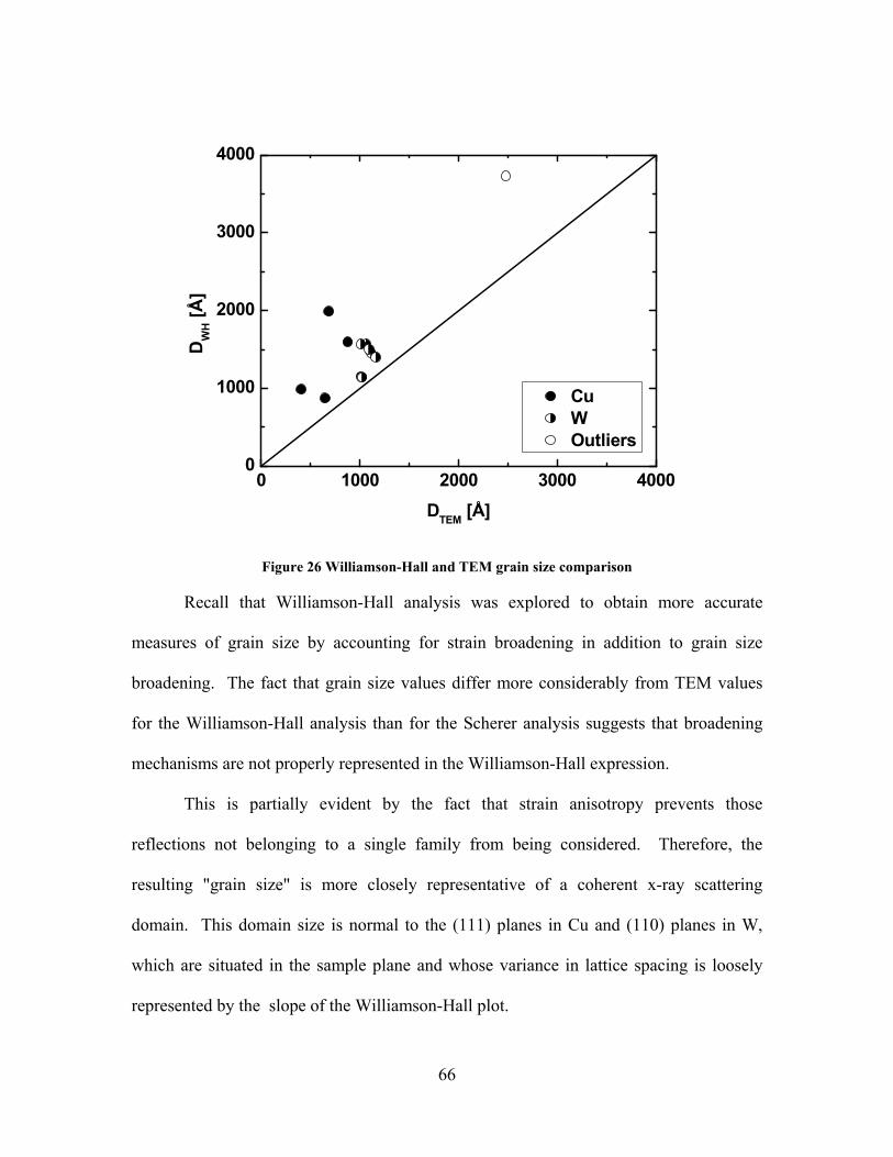
66
0 1000 2000 3000 40000
1000
2000
3000
4000
Cu W Outliers
DW
H [
Å]
DTEM
[Å]
Figure 26 Williamson-Hall and TEM grain size comparison
Recall that Williamson-Hall analysis was explored to obtain more accurate
measures of grain size by accounting for strain broadening in addition to grain size
broadening. The fact that grain size values differ more considerably from TEM values
for the Williamson-Hall analysis than for the Scherer analysis suggests that broadening
mechanisms are not properly represented in the Williamson-Hall expression.
This is partially evident by the fact that strain anisotropy prevents those
reflections not belonging to a single family from being considered. Therefore, the
resulting "grain size" is more closely representative of a coherent x-ray scattering
domain. This domain size is normal to the (111) planes in Cu and (110) planes in W,
which are situated in the sample plane and whose variance in lattice spacing is loosely
represented by the slope of the Williamson-Hall plot.

67
Evidence that broadening mechanisms are not properly treated in the Williamson-
Hall method additionally exists in the fact that that physical interpretation of the strain as
defined in equation ( 1-7 ) is vague: Its source cannot be attributed to any defect type
specifically. Exploration of a modified Williamson-Hall method is warranted, wherein
the microstrain is attributed to dislocations specifically.
4.3.2 Modified Williamson-Hall
Figure 27 (a,b) again present classical Williamson-Hall plots wherein all available
reflections are plotted to reveal data scattered by strain anisotropy. Figure 27 (c,d) rescale
the x-axis of the Williamson-Hall plots by the dislocation contrast factor [Ungár et al.
1996]. By inspection, this modified Williamson-Hall method provides improved
confidence in the measured slope and intercept of data's linear fit, in comparison to the
classical method.
An inherent assumption in the modified Williamson-Hall method is that strain
broadening is caused by dislocations. To generate the modified Williamson-Hall plots,
dislocation contrast values were calculated uniquely for each reflection (equation
( 1-12 )). Edge and screw dislocations were assumed to exist in equal amounts, and
necessary physical constants for dislocation contrast factor calculations were found in
literature [Overton et al. 1955], [Ungár et al. 1999].

68
Figure 27 Classical Williamson-Hall plots of Cu (a) and W (b) films: Strain anisotropy prevents monotonic function of peak width with Bragg angle. Modified Williamson-Hall plots of Cu (c) and W (d) films: Sscaling the peak position by the dislocation contrast reveals a monotonic function of
peak width with Bragg angle.
Comparing the grain size as determined by the modified Williamson-Hall method
provides an improved correlation to TEM data over the classical Williamson-Hall method
(Figure 28). As in previous figures, filled and half-filled circles represent Cu and W
films respectively.
To quantify the correspondence between TEM and Modified Williamson-Hall
measures of grain size a total sum squared error of 2.7106 was determined. The
improved correlation between TEM and XRD is significant when comparing the classical
and modified methods; indicating a significant contribution from dislocations to the
broadening of diffraction peaks. Nevertheless, the error obtained by the Modified
Williamson -Hall approach approach is still in excess of that obtained by the Scherrer
method. Therefore, while the Modified Williamson-Hall method attempts to attribute
0.6 0.8 1.0 1.2 1.4 1.60.001
0.002
0.003
0.004
0.005
0.006
0.007
K
K
0.6 0.8 1.0 1.2 1.4 1.60.0015
0.0020
0.0025
0.0030
0.0035
K
K
(111)
(222)
(220)
(311)
(110)
(220)
(200)
(211)
a)
b)
0.1 0.2 0.3 0.4 0.5 0.6 0.70.001
0.002
0.003
0.004
0.005
0.006
0.007
K
KC1/2
0.1 0.2 0.3 0.4 0.5 0.6 0.70.0015
0.0020
0.0025
0.0030
0.0035
K
KC1/2
(110)
(220)
c)
d)
(111)
(222)
(220)
(311)
(200)
(211)

69
stain broadening to physical sources of lattice distortion, the resulting grain sizes deviate
from actual values by an amount large enough so as to provides little advantage over
Scherrer first-order approximation.
0 1000 2000 3000 40000
1000
2000
3000
4000
Cu W
DM [
Å]
DTEM
[Å]
Figure 28 Modified Williamson-Hall Grain Size
4.4 Effects of Microstrain
The significant discrepancy between TEM and XRD measures of grain size
indicates the present of other mechanisms contributing significantly to peak broadening.
Because variations in lattice spacing have long been associated with peak broadening, the
contribution of microstrains to x-ray peak width are discussed in the context of thin films

70
on substrates. These are investigated in a novel manner, wherein the strain contribution
to peak width is isolated by first obtaining grain size directly from TEM.
4.4.1 Residual FWHM
TEM micrographs of Cu and W films in Figure 29 reveal considerable differences
in microstructures: The Cu specimen (Figure 29(a)), is a hollow cone dark field image,
used for TEM grain size analysis (Courtesy of Bo Yao; UCF) and corresponds to sample
Cu-03. The specimen is shown to possess an abundance of twins. Figure
29(b),correspond to a Orientation Index Map (OIM) of a W film, specifically sample W-
03, and was analyzed by ASTARTM (Courtesy of Xuan Liu; CMU). The micro structure
of Cu and W films clearly differs in that the W film lacks the abundant twin boundaries
that are apparent the Cu film.
Due to the varied defect structures observed between Cu and W films, coupled
with the fact that neither classical nor modified Williamson-Hall methods are able to
provide accurate grain size values, it may be expected that the x-ray line profile
broadening methods employed simply fail to accurately accommodate strain broadening.
Further investigations however reveal that this is not a proper conclusion.

71
Figure 29 (a) Cu-03 HCDF, (b) W-03 ASTAR OIM

72
To assess the degree to which the slope of the modified Williamson-Hall plots
correlate to strain-like broadening, let it be assumed that the measured peak width
represents a Gaussian convolution of grain size, instrumental, and residual (strain-like)
components:
2Residual
2Instrument
2GrainSizeMeasured Δ(2θ)Δ(2θ)Δ(2θ)Δ(2θ) ( 4-1 )
Having measured peak widths and instrumental broadening, the TEM grain size
may be used to calculate the residual peak width. This residual FWHM corresponds to
"extra" broadening, not accounted for in instrumentation or grain size; it therefore offers
a unique perspective on microstrain contributions to peak broadening. In the present
discussion, the second order reflection was considered for residual FWHM analysis; i.e.
the measured FWHM of a Cu(222) or W(220) reflection was used to determine grain size
and strain broadening contributions to the respective reflection. This approach was used
because higher order reflection are known to be more affected by strain effects than are
first order reflections. Calculated values for of residual FWHM (Δ(2θ)Res) are provided
in Table 7.
Table 7 Residual FWHM
IDTXRR[Å]
DTEM[Å]
Δ(2Θ)Res[°2Θ]
Cu‐01 270 405 0.260Cu‐02 336 684 0.389Cu‐03 371 648 0.277Cu‐04 417 877 0.241Cu‐05 451 1011 0.171Cu‐06 836 2215 0.241Cu‐07 1439 2480 0.144W‐01 189 1020 0.177W‐02 283 1060 0.223W‐03 425 1010 0.255W‐04 607 1110 0.237W‐05 1229 1090 0.209W‐06 1801 1160 0.200

73
The microstrain, as defined by the slope of the modified Williamson-Hall method,
strongly correlates to the calculated residual FWHM (Figure 30), and may be fitted by a
line with the following equation:
0.0662 + 38.627εΔ(2θ) MResidual ( 4-2 )
This strong correlation is indication that dislocations are indeed the primary
defect contributing to microstrains in these thin films, and are responsible for limiting
grain size analysis. The Cu specimens previously labeled "outliers" (Figure 22) also
conform to the trend set by all other Cu and W data. Figure 30 and its implications are
discussed further in the following section in terms of dislocation core spreading.
0.000 0.002 0.004 0.006 0.008 0.0100.0
0.1
0.2
0.3
0.4
0.5
Cu W Outliers
(2)
Res
. [o2
]
M
Figure 30 Residual FWHM closely tracks the Modified Williamson-Hall micro-strain: This indicates a contribution of dislocations to x-ray peak width.

74
While Figure 30 provides strong indication that dislocations, as determined by the
modified method of Williamson-Hall, contribute significantly to x-ray peak broadening,
the fact that the tend is linear with a non-zero intercept is noteworthy. Figure 31 replots
the data set presented in Figure 30, with superimposed curves indicating the expected
contributors of microstrain to peak broadening. Assuming four grain sizes (a) 250Å,
b)500Å, c) 1000 Å and d) 1010Å), the slope of the modified Williamson-Hall plot was
calculated for various microstrains. The peak broadening contribution of those
microsatrins was thus determined according the residual width method described above.
0.000 0.005 0.0100.0
0.1
0.2
0.3
0.4
0.5
Cu W Claculated
(d)
(c)
(b)
(a)
(2)
Res
. [o2
]
M
Figure 31 Contribution of microstrain to x-ray peak broadening. Circles indicate data, solid lines represented calculated contributions for grain sizes of a) 250Å b)500Å c) 1000 Å d) 1010Å
Because Cu and W data follow a single linear trend, despite the fact that they
span a range of grain sizes and microstrains, indicates that peak broadening mechanisms

75
in these thin films are not completely described by the modified Williamson-Hall
method. Nevertheless, the strong correlation between microstrain and residual width is
evidence of a significant and systematic microstrain contribution to peak width.
4.4.2 Dislocation Core Spreading
The attribution of strain broadening to dislocations, as described in the modified
Williamson-Hall method, results in an excellent correlation between the residual FWHM
and modified Williamson-Hall slope for all Cu and W films (Figure 30). This strong
correlation is noteworthy and warrants further discussion.
Figure 30 presents a dilemma in that the presence of dislocations is strongly
evident; yet recalling Figure 29, TEM observations are unable to support these
conclusions. The lack of observable dislocations in the TEM micrographs of Figure 29
may be attributed to the complex contrast exhibited in both figurers. Additionally, the
hollow cone dark field and ASTAR imaging methods used to generate the Cu and W
micrographs respectively may not be optimized for dislocation studies. In either case,
these TEM studies cannot be used to confirm a contribution of dislocations to x-ray peak
broadening. Additionally, the modified Williamson-Hall method resulted in grain size
values whose correspondence to TEM measures was poorer than that obtained by
Scherrer analysis. The validity of the modified Williamson-Hall method can therefore
easily be disregarded for thin films, though doing so would be premature.
In addition to the aforementioned imaging-based limitations to detecting
dislocations in these Cu and W specimens, it is hypothesized that dislocation core
spreading at the film/substrate interface may be additionally impeding their observance
by TEM. The disappearance of dislocation contrast is not without precedent [Müllner et

76
al. 1998]. Müllner et. al. reported dislocations along interfaces in Al systems which were
seen to disappear under electron beam irradiation: The disappearing contrast was
attributed to spreading of the dislocation core.
The fact that thin films often exhibit unique mechanical properties has often been
attributed to dislocations. In most descriptions, dislocations are treated as 1-dimentional,
compact defects. The concept of dislocation core spreading was however described as
early as 1949 [Eshelby 1949]. A theoretical considerations of the spreading of
dislocation cores at film/substrate interfaces were published over 50 years later [Gao et
al. 2002]. Figure 32 illustrates a simple example of an edge dislocation at an interface.
When the adhesion (or coherency) between film and substrate is high, the dislocation will
remain compact. Such is the case with epitaxial films (Figure 32(a)). In the case of an
edge dislocation at a film/(amorphous) substrate interface, where adhesion and coherency
are low (Figure 32(b)) viscous sliding may take place between film and substrate,
allowing the otherwise compact core to spread into many infinitesimal dislocations
(Figure 32(c)). The significance of dislocation core spreading on the mechanical
properties of thin films was discussed in a recent review paper [Wang et al. 2011].

77
Figure 32 Edge Dislocation at a film/substrate interface (a) epitaxial interface with compact dislocation core, i.e. a point defect (b) An edge dislocation at a crystalline/amorphous interface (c) a
spread dislocation core at a crystalline/amorphous interface
The extent of dislocation core spreading was characterized by Gao, and select
solutions to equilibrium core widths have been published [Gao et al. 2002], [Gupta
2005]. Equation ( 4-3 ) represents the equilibrium core width for edge dislocations in an
a)
b)
c)

78
array separated by a distance L. Figure 33 presents a schematic where the dotted circles
represent the width of a spread edge dislocation core along a film/substrate interface.
Figure 33 Spread edge dislocation cores of width W in array separated by a distance L
In equation ( 4-3 ), the amorphous substrate and metallic film are assumed to have
equivalent mechanical properties, i.e. Young's modulus (E) and Poisson's ratio (). The
interface strength is represented by 0, which was taken to equal 140MPa for Cu and
153MPa for W: This is based on adhesion studies in damascene Cu structures
[Lanckmans et al. 2002]. The Burgers vector (b) was calculated to equal 2.55Å for Cu
using a lattice parameter of 3.61Å and the [110] close pack direction. For W, b is
calculated to equal 2.74Å using a lattice parameter of 3.16Å and the [111] close pack
direction. Bulk values of E and were assumed for Cu and W.
L)τυ8(1
πEbtanhsin
π
LW
02
1ρ
( 4-3 )
The distance between dislocations ( L ) was determined from the dislocation density
(M), which was calculated from the slope of the modified Williamson-Hall plot and
equation ( 1-14 ):
1/2ρ ρL ( 4-4 )
W L
Film
Substrate

79
Using equations ( 4-3 ) and ( 4-4 ), equilibrium core widths have been calculated
for all Cu and W samples and the results are summarized in Table 8, which additionally
includes calculated dislocation densities and dislocation separations.
Table 8 Dislocation in Cu and W films
ID M[m‐2]
L[Å]
W[Å]
Cu‐01 1.9E+13 2308 355Cu‐02 4.3E+13 1522 338Cu‐03 1.7E+13 2426 356Cu‐04 1.3E+13 2798 359Cu‐05 3.0E+12 5777 367Cu‐06 1.3E+13 2752 359Cu‐07 3.7E+12 5192 366W‐01 5.3E+12 4364 365W‐02 1.2E+13 2924 360W‐03 1.7E+13 2415 356W‐04 1.3E+13 2810 359W‐05 9.9E+12 3178 361W‐06 7.5E+12 3640 363
Core widths are found to\ be on the order of 300Å, irrespective of film thickness,
grain size or crystallographic structure (Figure 34 (a)).
The fact that core widths are essentially constant with thickness (not shown) and
(TEM) grain size (Figure 34), means that outliers from previously discussed grain size
data may be accounted for: Figure 34(b) indicates that Scherrer grain size analysis
becomes limited as a grains becomes populated with multiple dislocations. It may thus
be hypothesized that dislocations contribute to coherency disruptions, which contribute to
the poor correlations between TEM and X-ray based grain size metrology methods.

80
Figure 34 Dislocation Core Width and Grain Size. The core width is constant with (a) TEM and (b)
Scherrer grain size. The Scherrer grain size becomes limited as the real grain size, i.e. the TEM
grain size, becomes large enough so as to accommodate multiple dislocation cores.
0 1000 2000 3000200
300
400
500
Cu W Outliers
W
[Å]
DTEM
[Å]
0 1000 2000 3000200
300
400
500
Cu W Outliers
W
[Å]
DS [Å]
a)
b)

81
4.4.3 Intra-Grain Misorientations
To further elucidate the effect of dislocation core spreading at film/substrate
interfaces and its effect on x-ray profile analysis, a yet un-discussed sample set of W thin
films will now be considered. The specimens currently under discussion have been
prepared by Global Foundries.
Table 9 GF-W Peak fitting results
ID λ[Å]
Δ(2Θ)110[°2Θ]
2Θ110[°2Θ]
Δ(2Θ)220[°2Θ]
2Θ220[°2Θ]
GFW2 0.575 40.095 0.996 86.613
GFW4 0.756 40.163 1.696 86.826
GFW5
Cu‐Kα
0.66 40.146 1.342 86.771
The sample set is limited to three specimens wherein complete TEM and XRD
data sets were available for comparison. Results of peak profile fitting are presented in
Table 9. Results of grain size analysis (Scherrer analysis with k=1.00, and Modified
Williamson-Hall); the slope of the modified Williamson-Hall plot; calculated values of
residual FWHM; dislocation density; average dislocation separations; and equilibrium
dislocation core width are listed in Table 10. Film thicknesses and TEM grain sizes are
also included.
Table 10 GW-W results of X-ray Line Profile Analysis
IDTTotal [Å]
DTEM[Å]
DS(k=1.00)[Å] DM[Å] M
Δ(2Θ)Res.[°2Θ] M[m‐2] L
[Å]W[Å]
GFW2 134 830 192 383 0.016 0.938 2E+14 676 234GFW4 129 820 135 962 0.039 1.663 1E+15 278 133GFW5 127 810 160 572 0.028 1.299 7E+14 391 174

82
High quality TEM images and corresponding inverse pole figure maps of the
three GF-W samples discussed above have been collected using ASTAR (Courtesy of
Xuan Liu): Figure 35 shows representative orientations maps of GF-W samples -02, -04,
and -05 in Figures (a), (b) and (c) respectively. False color is indicative of
crystallographic orientation; a key is provided in Figure 35(d).
Figure 35 ASTAR inverse pole figure maps of (a) GF-W2 (b) GF-W4 (c) GF-W5 Showing intra-rain misorientations. (d) Key.

83
Grain boundaries are established by setting a 5° tolerance angle. The TEM
investigation does not reveal dislocations. Instead, single grains are observed in which
intra-granular distortion of the lattice are reported to exceed 50°. Such misorientation
angles would be expected to result in geometrically necessary dislocations [Nye 1953],
and will be considered in future work. Figure 36 shows a single grain from GF-W-05,
where the relative orientation within the single grain was measured at 10 distinct points:
Table 11 represents a matrix specifying the measured relative orientations.
Figure 36 ASTAR inverse pole figure maps of a single grain in sample GF-W-05. The numbers 1 - 10 indicate locations where relative orientations were measured and are tabulated in Table 11.

84
Table 11 Relative Misorientation angles 1 2 3 4 5 6 7 8 9 101 16.3 13.9 25.2 32.1 43.2 50.5 46.4 41.3 38.82 16.3 2.4 9.3 16.6 41 35.3 31.6 27.1 26.83 13.9 2.4 11.4 18.7 43.3 37.4 33.6 29 28.34 25.2 9.3 11.4 9.8 31.9 27.8 24.7 21.7 245 32.1 16.6 18.7 9.8 27.6 18.7 15.2 11.9 15.56 43.2 41 43.3 31.9 27.6 20 23.2 28 367 50.5 35.3 37.4 27.8 18.7 20 4.7 10.9 18.48 46.4 31.6 33.6 24.7 15.2 23.2 4.7 6.3 149 41.3 27.1 29 21.7 11.9 28 10.9 6.3 8.110 38.8 26.8 28.3 24 15.5 36 18.4 14 8.1
Sub-grain distortions have been experimentally published in the past: These
reports have focused on large grained (in excess of 100m) bulk specimens and followed
their inter- and intra-granular deformations as a function of loading conditions [Hofmann
et al. 2009], [Korsunsky et al. 2012]. Intra-grain lattice distortions in polycrystalline thin
films, on nanometric scales have not been previously reported.
The effect of these observed intra-grain distortions on the grain size measurable
by line profile analysis is significant. Briefly considering the rocking of a specimen
through the Bragg angle, is instructive [Warren 1990].
Figure 37 Schematic of a rocking curve experiment.
If a single-crystal specimen is rocked from low to high angles, and the detector
remains fixed at the Bragg position; an increase in x-ray intensity will be observed as the
∆θ
θB 2θB
Nd

85
sample angle approaches 1/2 of the Bragg angle, θB, and likewise decreases upon moving
the specimen to higher angles. In the case where the specimen is smaller than the
incident beam, The width of this "rocking curve" is influenced by the length of the
crystal. Figure 37 presents a schematic of the situation, where N is the number of lattice
planes, and d is the lattice spacing. The following equation can then be used to estimate
the width of the rocking curve: Or rather, it can estimate the critical angular range, ΔθC,
beyond which the Bragg condition is no longer satisfied:
B
C 2Nasinθ
λΔθ
( 4-5 )
The rocking curve concept may be applied to the intra-grain distortions discussed
above. Let sub-grain lattice distortions be approximated by rigid, tilted planes. Consider
a single crystallite of length D, and height (i.e. thickness) t, whose constituent lattice
planes are each tilted with respect to one another about a common axis that is pointing
out of the page (Figure 38). Attempts to measure D by x-ray methods will be
unsuccessful because a portion of the planes are tilted beyond the critical angle, ΔθC.
This break in coherency of the crystal from the perspective of the incident x-rays means
that underestimated values of grain size will ultimately be measured. Specifically, N'
planes with spacing d, will be seen as the coherent scatting domain.

86
Figure 38 Schematic of critical misorientation angle effect on grain size measured by x-ray diffraction
In this approximation of a distorted crystal, the rocking curve equation may be
applied. Using sample GF-W-05 as an example, t is film thickness (127Å), and Nd=D is
the TEM grain size (1304Å). Using Cu-Ka radiation, and solving equation ( 4-5 ), ΔθC is
found to be approximately 1°. In this context, ΔθC takes on the meaning of a critical
intra-grain misorientation angle, beyond which the lattice planes no longer satisfy the
Bragg condition with the incident beam. It is worth noting that rocking curve
experiments on plastically deformed Cu single crystals have also reported that
misorientations of only 1° are sufficient to terminate coherency [Wilkens et al. 1987].
Recall that intra-grain misorientations of up to 50° were observed in this specimen, which
is far in excess of the calculated critical value. Additionally, recall that the measured
Scherrer grain size for this sample was 168 Å, far short of the expected 1304Å. It may
thus be concluded that the observed misorientations have a significant effect of the
meaning and utility of x-ray based grain size analysis.
∆θ
N’d
Nd=D
t

87
Coherency disruptions resulting from distortions within a crystal have been
considered in terms of the effect on x-ray grain size analysis in plastically deformed
metals [Ungár et al. 2012]. It was reported that dislocations in dipolar wall
configurations result in x-ray phase shifts and peaks are therefore broadened by "sub-
grains." While these reports are analogues to the present situation, and offer a conceptual
framework for the present discussion, this prior work focused on specimens with grain on
the order of 10 and were representative of plastically deformed metals, rather than
nanometic metallic thin films [Hughes et al. 1991].
0.000 0.025 0.0500.0
0.5
1.0
1.5
2.0
Cu W GF-W
(2)
Res
. [o2]
m
Figure 39 Strong Correlation of Res. FWHM to the Mod. W-H slope; all samples
The detailed TEM analysis of these GF-W samples may also be used revisit the
concept of residual FWHM and its implications for grain size analysis. Figure 39 re-plots

88
the data from Figure 30 and its linear fit: It additionally includes GF-W specimens for
comparison. The residual FWHM of the GF sample set not only strongly correlates to the
slope of the modified Williamson-Hall, but closely follows the trend set by the Cu and W
films discussed in previous sections. This further indicates the influence of dislocations
on the film and their effect on x-ray profiles. It should be stressed that the strong
correlation between residual FWHM and modified Williamson-Hall slope is comparable
for all thin films explored; irrespective of crystallographic structure, atomic number, or
diffractometer.
4.5 Empirical Grain Size Calculation; A Novel Line Profile Method
Because the residual width so closely follows the slope of the modified
Williamson-Hall plot, it is possible to employ this empirical observation to formulate a
novel line profile analysis strategy for measuring the grain size of thin films. The slope
of a line depicted in Figure 39 is equal to 38.627, with an intercept of 0.0662 (equation
( 4-2 )).
The grain size contribution to peak broadening was thus calculated using (1)
equation ( 4-2 ); (2) the instrument function (Figure 1); and (3) the measured peak width,
peak positions, and TEM grain sizes from Table 3. Using the Scherrer equation and
inserting the measured peak position and corresponding calculated FWHM, a calculated
empirical grain size is obtained. Table 12 lists grain sizes calculated by this method; a
graphical comparison of TEM and empirical grain size values (DEmp-) are presented in
Figure 40. The solid line in Figure 40 indicates a hypothetical perfect correspondence
between x-ray and TEM grain sizes.

89
Table 12 Empirical grain size; calculated from M
IDDTEM[Å] DEmp‐[Å]
Cu‐01 405 420Cu‐02 684 633Cu‐03 648 599Cu‐04 877 846Cu‐05 1011 852Cu‐06 2215 2095Cu‐07 2480 0W‐01 1020 1000W‐02 1060 1216W‐03 1010 1231W‐04 1110 1107W‐05 1090 1260W‐06 1160 1109GFW2 830 185GFW4 820 216GFW5 810 188
0 1000 2000 30000
1000
2000
3000
Cu W GF-W
DE
mp
- [
Å]
DTEM
[Å]
Figure 40 Empirical grain size; calculated from M
Using this novel empirical method of line profile analysis, a strong correlation
between TEM and x-ray measures of grain size is obtained. The sum squared error for

90
this method is calculated to be 8.4106. This value is comparable to that obtained by the
Modified Williamson-Hall method, when its error is calculated for all samples including
the GF specimens (3.7106). It should be noted that a single Cu specimen, Cu-07, fails to
be measurable by this method. This is attributed to The fact that the measured FWHM is
essentially equal to the calculated residual FWHM, likely indicating that the narrow peak
is almost entirely broadened by defects. Accordingly, a grain size value of 0 has been
assigned in Table 12, Figure 40, and used for error calculations.
Similarly, the GF-W samples have large grain sizes, and high dislocation
densities, in comparison to the instrumental resolution. Nevertheless, the strong
correlation between microstrain and the residual width motivates further development of
dislocation-based empirical strategy for grain size analysis by line profile methods.
Error! Reference source not found. is presented as a summary of the line profile
methods explored. It lists the total sum squared error between TEM and x-ray-based
analyses of grain size.
Table 13 Comparison errors for all Line Profile Methods
LineProfileMethod Σχ²
Scherrer(k=1.00) 5.5.E+06
Scherrer(k=1.055) 2.6.E+06
Williamson‐Hall 1.4.E+09
ModifiedWilliamson‐Hall 3.7.E+06
Empirical(M) 8.4.E+06

91
Because the slope of the modified Williamson-Hall plot is understood to
correspond to dislocation density, a graph similar to Figure 39 may be generated in which
the residual width is plotted as a function of dislocation density directly. Figure 41
presented such a graph, which also includes a logarithmic fit to all data.
1E12 1E13 1E14 1E15 1E160.0
0.5
1.0
1.5
2.0
Cu W GF-W
(2)
Res
. [o2
]
M [m-2]
Figure 41 Residual FWHM and Dislocation Density
The equation of the fitted line in Figure 41 is displayed as equation ( 4-6 ).
)106.90075(ρ-0.51773Ln -16.38201Δ(2θ) 13MRes. ( 4-6 )
The fit is strongly indicative of a significant contribution to peak broadening
stemming from dislocations. This work may be supplemented by considering dislocation
density analysis by non-x-ray methods: Specifically TEM based analysis.

92
Preliminary investigations have been carried out into the correlation between
dislocation density analysis based on TEM and X-ray diffraction. The TEM analysis
were performed by Xuan Liu of CMU, and are based on a the Read-Shockley model of
dislocations [Read et al. 1950]. More sophisticated analysis will be perused, which will
be based on the Nye model of Geometrically Necessary Dislocations [Nye 1953].
Figure 42 presents a summery of the preliminary comparison between TEM and
x-ray measures of dislocation density. Specifically, all GF-W samples are plotted along
with sample W-03. While the values obtained by the Read-Shockley method are higher
than that obtained by the modified Williamson-Hall method, a correlation is nevertheless
evident. In terms of further developments warranting consideration for x-ray based
analysis, the exact value of the constant A in equation ( 1-14 ) may be investigated.
Specifically, the constant A in equation ( 1-14 ) was assumed to equal 10 for all samples.
As stated in section 1.1.2.3 Williamson-Hall plotthis constant may vary by almost an
order of magnitude: This translates to almost an order of magnitude uncertainty in the
dislocation density itself. Continued efforts in are therefore motivated.
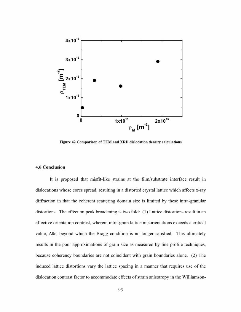
93
0 1x10¹⁵ 2x10150
1x10¹⁶
2x10¹⁶
3x10¹⁶
4x10¹⁶
TE
M [
m-2]
M [m-2]
Figure 42 Comparison of TEM and XRD dislocation density calculations
4.6 Conclusion
It is proposed that misfit-like strains at the film/substrate interface result in
dislocations whose cores spread, resulting in a distorted crystal lattice which affects x-ray
diffraction in that the coherent scattering domain size is limited by these intra-granular
distortions. The effect on peak broadening is two fold: (1) Lattice distortions result in an
effective orientation contrast, wherein intra-grain lattice misorientations exceeds a critical
value, Δθc, beyond which the Bragg condition is no longer satisfied. This ultimately
results in the poor approximations of grain size as measured by line profile techniques,
because coherency boundaries are not coincident with grain boundaries alone. (2) The
induced lattice distortions vary the lattice spacing in a manner that requires use of the
dislocation contrast factor to accommodate effects of strain anisotropy in the Williamson-

94
Hall plot. The speading of dislocation cores across the film/substrate interface would
render them invisible to TEM investigations. Precession Electron Diffraction Orientation
Maps in TEM studies of W films however, reveal intra-granular distortions whose
misorientaion angles approach 50° across a grains whose diameters are approximately
1000Å. Calculations suggest a dislocation core width on the order of a few hundred
Angstroms, independent of films thickness, or grain size. The poor correlation between
TEM and x-ray measures of grain size may also be explained: When the (TEM) grain
size is smaller than the dislocation core width, grain boundaries are the dominant
mechanism by which coherency is disrupted. As the grains size increases and multiple
dislocations are present within grains, coherency across the length of the crystallite is
disrupted. Because x-rays "see" coherent domains, accurate measures of grain size are
limited to specimens where the coherent scattering domains are established
predominately by grain boundaries. In the case of thin films with very large grains, grain
boundaries only represent a fraction of these coherency boundaries.
Finally, the effect of dislocations to broaden diffraction peaks, and hence limit
grin size analysis, may be taken advantage of. A novel residual peak width parameters
has been developed to provide insight into the broadening effects of dislocations. The
strong correlation between residual peak width and the slope of the modified Williamson-
Hall plot was used to developed an empirical method for determining grain size. This
empirical method was additionally extended to consider the dislocation density directly.
A significant decrease in the sum squared errors between TEM and x-ray based grain
sizes values obtained by these empirical methods are encouraging and warrant further
development.

95
CHAPTER FIVE : INTERFACE MORPHOLGY ANALYSIS
The morphological evolution of chemically stable metal/air or metal/vacuum
interfaces (free surfaces) with annealing temperature and/or time have been explored in
the past [Nichols et al. 1965], [Balluffi et al. 2005], [Jiran et al. 1990]. Relatively little
work has been done however, to extend that understanding to chemically stable buried
interfaces. The tendency for systems to reduce their free energy by minimizing surface
area, i.e., capillarity, should have an important role in the evolution of buried interfaces
as it does for free surfaces. However, for buried interfaces two solids are present and
their morphology is mechanically coupled. The role of mechanical coupling to modify
the evolution of buried interfaces is of significant interest to many nano-scaled system
and to semiconductor interconnections in particular.
5.1 Objectives
The objective of this research is to understand the morphological evolution of
nanometric Cu film surfaces and interfaces, and to develop a fundamental understanding
of the role that annealing plays on the evolution of solid/solid interfaces
5.2 Results
5.2.1 Qualitative Observations
X-ray scattering techniques reveal significant differences in the interfacial
evolution of Cu thin films encapsulated by SiO2 as compared to those encapsulated by
Ta/SiO2. Qualitative conclusions regarding RMS roughness can be drawn by simple
inspection of the specular patterns. Annealing SiO2 encapsulated films at 600°C results

96
in a smoother Cu/SiO2 interface, as can be seen from the slower decay of specular
intensity as compared to its 150°C counterpart (Figure 43(a)). Ta/SiO2 encapsulated
films change little upon annealing (Figure 43(c)).
The specular intensity profiles were modeled (solid lines) to allow for quantitative
values of thickness, σupper and σlower for the Cu layers to be determined (Table 14). Figure
43(b and d) shows experimentally obtained rocking-curves (circles) and calculated
spectra (solid lines). These diffuse X-ray reflectivity scans were modeled to determine
the lateral correlation length of roughness, the vertical correlation fraction and the fractal
exponent. The specular reflection in the diffuse spectra at Qx=0 is broadened by
instrument resolution and contains no quantitative information regarding the sample and
was therefore excluded from the analysis. Qualitative trends can be observed by
inspection of the diffuse patterns. For SiO2 encapsulated Cu film, the diffusely scattered
intensity for the sample annealed at 600°C (open circles) decays more quickly than at
150° (filled circles). Simply put, at 150°C the spectrum is essentially flat, and is concave
at 600°C. Given that the intensity of scattered X-rays is proportional to the square of the
interface roughness amplitude, inspection of the diffusely scatter intensity distribution for
SiO2 encapsulated films suggests a decay in roughness amplitude that depends on the
lateral length scale of the roughness.

97
-0.01 0.00 0.010.01
0.1
150°C 600°C Fit
No
rmal
ized
Inte
nsi
ty
Qx[Å-1]
b)
-0.01 0.00 0.010.01
0.1
150°C 600°C Fit
No
rma
lize
d In
ten
sit
y
Qx[Å-1]
d)
Figure 43 X-ray reflectivity spectra(a,b) SiO2/Cu/SiO2 (c,d) SiO2/Ta/Cu/Ta/SiO2
Before discussing quantitative results and their interpretations, the following
conclusion should be kept in mind which can be drawn by simple inspection of the
specular and diffuse X-ray reflectivity spectra: Annealing at 600°C results in a
roughness-wavelength dependent decrease in roughness amplitude for Cu/SiO2
interfaces. These observations are consistent with that predicted by capillarity driven
surface diffusion and smoothening [Nichols et al. 1965]. The apparent lack of interface
morphology evolution in the Cu/Ta interface is also noted.
To confirm, quantify, and interpret these observations, specular and diffuse x-ray
reflectivity patterns were modeled using commercially available software: Results of
0.0 2.5 5.0
10-6
10-2
102
150°C 600°C Fit
No
rmal
ized
In
ten
sity
°2
a)
0.0 2.5 5.0
10-8
10-4
100
150°C 600°C Fit
No
rmal
ized
In
ten
sity
°2
c)

98
modeling can be found in Table 14. Error bars for reflectivity results are quoted at a 90%
confidence level. Grain size values are provided for reference; a single asterisk (*)
denotes grain sizes calculated from resistivity data [Sun 2009], a double asterisk (**)
indicates samples characterized by GID in chapter 4.
Table 14 Results of fitting X-ray reflectivity spectra. Grain sizes based on TEM. a)SiO2/Cu/SiO2;150°C
Thickness[Å]
GrainSize[Å]
σupper[Å]
σlowerr[Å]
ξlateral[Å]
α ξvertical
270±2 **405±25 12±1 8±1 381±46 0.8±0.2 0.4±0.4312±1 *409±24 10±1 7±1 203±18 0.9±0.2 0.5±0.5353±3 543±21 11±1 10±1 319±40 0.9±0.2 0.7±0.1451±2 **1011±46 10±1 8±1 287±33 0.9±0.2 0.4±0.1718±2 1718±79 7±1 12±2 492±57 0.9±0.2 0.6±0.21439±3 **2481±172 7±1 26±1 616±113 0.9±0.2 0.5±0.3
b)SiO2/Cu/SiO2;600°C292±1 *305±15 3±1 8±1 318±90 0.6±0.2 0.6±0.1336±5 **684±44 2±2 7±1 412±56 0.9±0.1 0.5±0.5369±3 814±45 5±1 10±2 420±112 0.9±0.2 0.9±0.1464±1 1126±77 4±1 9±1 561±65 0.9±0.2 0.6±0.2745±1 2200±95 3±1 10±1 706±62 0.5±0.2 0.5±0.31499±1 4252±157 3±1 10±1 798±62 0.8±0.2 0.1±0.1
c)SiO2/Ta/Cu/Ta/SiO2;150°C281±7 *681±34 8±1 15±3 316±46 0.4±0.2 0.2±0.2335±1 *376±19 2±1 6±1 401±41 0.4±0.2 0.5±0.1370±9 *814±45 15±5 10±2 606±57 0.4±0.2 0.5±0.5482±4 *1126±77 11±1 10±1 326±38 0.7±0.2 0.3±0.1762±2 *2200±95 15±1 16±5 687±78 0.4±0.2 0.3±0.11541±5 *4659±172 22±1 22±3 864±77 0.6±0.2 0.5±0.5
d)SiO2/Ta/Cu/TaSiO2;600°C283±2 346±17 8±1 11±1 412±56 0.9±0.2 0.5±0.5342±4 394±17 11±1 12±2 489±53 0.8±0.2 0.5±0.5387±5 443±22 15±4 10±1 612±58 0.5±0.2 0.6±0.4484±3 696±34 10±1 10±1 599±125 0.9±0.2 0.5±0.2779±0 1101±46 14±2 12±3 773±94 0.5±0.2 0.5±0.51552±3 3451±150 9±1 15±2 891±79 0.9±0.2 0.5±0.2
In Table 15 each entry represents an average of six sister samples (i.e. a total of
24 samples are represented) whose thicknesses were intentionally varied from 27Å to
1580Å. Error bars correspond to the average error from each set of six sister samples.

99
Table 15 Average roughness values for SiO2 and Ta/SiO2 encapsulated Cu films.
SiO2/Cu/SiO2
150°CSiO2/Cu/SiO2
600°CTa/Cu/Ta
150°CTa/Cu/Ta
600°C
σupper[Å] 10±1 3±1 14±2 11±2
σlowerr[Å] 12±1 9±1 14±2 12±2
Ξ[Å] 383±38 533±53 523±5 588±6
ξV 0.50±0.10 0.40±0.10 0.10±0.10 0.20±0.10
α 0.9±0.1 0.7±0.3 0.5±0.2 0.7±0.2
5.2.2 Statistical Characterization of Film Growth
Having obtained numeric solutions of the correlation function, studying the
effective growth dynamics within the thickness rage from 280Å to 1580Å is possible.
Although the relatively small data set limits any conclusion to being semi quantitative,
the consequence of barrier layer and annealing temperature on the effective growth
dynamics can nonetheless be observed.
Given equation ( 1-16 ), ztt /1~)( , the determination of the dynamic exponent z
is achieved by fitting a power law to experimentally obtained values of )(t . Note that
the time for growth, t, corresponds to the deposition time for the thin film. If a constant
deposition rate is assumed, film thickness is directly proportional to deposition time.
Plotting as a function of thickness (which has been normalized to the thickest film) can
accordingly be used to determine z . Accordingly, the correlation length as a function of
normalized deposition time has been plotted in Figure 44(a) for Cu/SiO2, and Figure
44(b) for Cu/Ta. Normalizing each data set (Figure 44(c)) highlights the fact that a
single dynamic exponent value can be used to fit each data set, irrespective of barrier
layer and annealing conditions. Here 0 represents the proportionality constant that

100
makes the relation, ztt /1~)( , an equality, which then corresponds to the lateral
correlation length at time t0.

101
Figure 44 Power law scaling of correlation length; self affine behavior
1 2 3 4 5 6
200
400
600
800
1000 150°C 600°C
z150°
= 2.0±0.6
z600°
= 2.2±0.4
[Å
]
Normalized Deposition Time
a)
1 2 3 4 5 6200
400
600
800
1000 150°C 600°C
z150°
= 2.0±0.6
z600°
= 2.6±0.4
[Å
]
Normalized Deposition Time
b)
1 2 3 4 5 60.5
1.0
1.5
2.0
2.5
3.0
z = 2.2±0.3
No
rmal
ized
Normalized Deposition Time
c)
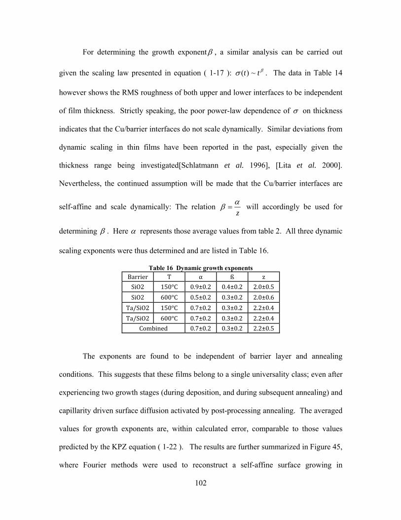
102
For determining the growth exponent , a similar analysis can be carried out
given the scaling law presented in equation ( 1-17 ): tt ~)( . The data in Table 14
however shows the RMS roughness of both upper and lower interfaces to be independent
of film thickness. Strictly speaking, the poor power-law dependence of on thickness
indicates that the Cu/barrier interfaces do not scale dynamically. Similar deviations from
dynamic scaling in thin films have been reported in the past, especially given the
thickness range being investigated[Schlatmann et al. 1996], [Lita et al. 2000].
Nevertheless, the continued assumption will be made that the Cu/barrier interfaces are
self-affine and scale dynamically: The relation z
will accordingly be used for
determining . Here represents those average values from table 2. All three dynamic
scaling exponents were thus determined and are listed in Table 16.
Table 16 Dynamic growth exponents Barrier T α ß z
SiO2 150°C 0.9±0.2 0.4±0.2 2.0±0.5
SiO2 600°C 0.5±0.2 0.3±0.2 2.0±0.6
Ta/SiO2 150°C 0.7±0.2 0.3±0.2 2.2±0.4
Ta/SiO2 600°C 0.7±0.2 0.3±0.2 2.2±0.4
Combined 0.7±0.2 0.3±0.2 2.2±0.5
The exponents are found to be independent of barrier layer and annealing
conditions. This suggests that these films belong to a single universality class; even after
experiencing two growth stages (during deposition, and during subsequent annealing) and
capillarity driven surface diffusion activated by post-processing annealing. The averaged
values for growth exponents are, within calculated error, comparable to those values
predicted by the KPZ equation ( 1-22 ). The results are further summarized in Figure 45,
where Fourier methods were used to reconstruct a self-affine surface growing in

103
accordance with dynamic scaling laws whose exponents are equal to those of the
combined values from Table 16. Specifically, Figure 45 illustrates five distinct time-
slices of a growing rough surface for which the amplitude of roughness and lateral
correlation length increase in accordance with the combined values from Table 16.
-50 -25 0 25 50
0
1
2
3
4
No
rmal
ized
su
rfac
e h
eig
hts
Normalized crossectional length
Figure 45 Surface growth reconstruction based on exponents from table 3
Additional investigation of the scaling of thin films may be pursued by
considering grain size. In following the convention of Figure 44, Figure 46 presents the
correlation length plotted as a function of grain size which has been normalized such that
the larges measured grain size is equal to 1. While investigating grain growth dynamics
is beyond the scope of this work, it is nonetheless worthwhile to look for trends.

104
Figure 46 Power law scaling of correlation length with grain size
0 2 4 6 8 10
200
400
600
800
1000
150°C 600°C
z150°
= 2.3±0.7
z600°
= 2.6±0.5
[Å
]
Normalized Grain Size
a)
0 2 4 6 8 10
200
400
600
800
1000
150°C 600°C
z150°
= 2.2±0.7
z600°
= 3.5±0.9
[Å
]
Normalized Grain Size
b)
0 2 4 6 8 10
0.5
1.0
1.5
2.0
2.5
3.0
z = 2.8±0.4
No
rmal
ized
Normalized Grain Size
c)

105
Fitting the grain size data with a power law yields exponent values that are
equivalent to those obtained for film thickness. This result is consistent with an
incomplete decoupling of film thickness from grain size [Sun et al. 2009]. Normalizing
each data set (Figure 46(c)), highlights the fact that a single dynamic exponent value can
be used to fit each data set, and is equivalent, within statistical error, to that obtained in
Figure 44(c). Although these results are not used to identify a universality class for grain
growth, they do suggest a fundamental scaling relationship between grain size, film
thickness, and lateral roughness[Lita et al. 2000].
5.2.3 Interface Smoothening
When comparing results from modeling specular reflectivity profiles, the most
noteworthy trend is that of RMS roughness and annealing. Figure 6 presents average
RMS roughness values from table 2 plotted as a function of anneal temperature. For SiO2
encapsulated films, significant changes upon annealing at 600°C are observed (Figure
47(a)). Firstly, σupper is observed to decrease significantly in comparison to σlower. This is
attributed to the fact that the bottom Cu/SiO2 interface, although chemically identical to
the top, is attached to a rigid substrate which mechanically hinders changes in interfacial
topography. For Ta/SiO2 encapsulated films, σupper and σlower are not only comparable to
one another, but also fail to evolve significantly upon annealing (Figure 47(b)).

106
Figure 47 Average RMS roughness (a) SiO2 and (b) Ta/SiO2 encapsulated Cu films
150 6000.0
0.5
1.0
1.5
2.0
[
Å]
Anneal Temp [°C]
upper
lower
a)
150 6000.0
0.5
1.0
1.5
2.0
[
Å]
Anneal Temp [°C]
upper
lower
b)

107
These observations for the upper Cu/SiO2 interfaces point toward capillarity as a
driving force for surface smoothening; an increase in lateral correlation length is
therefore expected to correspond to the decrease in roughness amplitude upon annealing.
Figure 48(a) depicts such an increase in correlation length corresponding to a
decrease in RMS roughness with annealing for the upper Cu/SiO2 interface, thus
motivating a more detailed investigation of the Mullins theory of surface smoothing. No
smoothing trend is apparent for Cu/Ta interfaces Figure 48 (b).

108
Figure 48 Correlation length and. roughness of (a) Cu/SiO2 and (b) Cu/Ta/SiO2
Figure 49 presents simplified illustrations to supplement and highlight the
observed effects of annealing. A single sinusoidal wavelength, λ , is used to represent
0 5 10 15 20 25
200
400
600
800
1000
150°C 600°C
[Å
]
upper
[Å]
0 5 10 15 20 25
200
400
600
800
1000
150°C 600°C
[Å
]
upper
[Å]
a)
b)

109
the more complex topography of the interface summarized by the lateral correlation
length, ξ. In summary: Upon annealing, σupper of the Cu/SiO2 interface decreases while
σlower remains unchanged. The wavelength λ increase observed upon annealing is
presumed to be that of the upper interface. However, while the RMS changes are
distinguishable for the upper and lower interfaces, the same is not true for the changes in
lateral correlation length, which is not experimentally distinguished between upper and
lower interfaces. The Cu/Ta interfaces are consistent between top and bottom, and do not
change upon annealing.
Figure 49 Illustration of film interfaces displaying capillarity effects
The results are quantitatively summarized in Figure 50, wherein Fourier methods
were used to reconstruct the upper Cu/SiO2 self-affine interface decaying in accordance
with the results from Table 16. Specifically, the correlation length is shown to increase by
28%, while the RMS roughness is shown to decrease linearly by 70%.

110
-50 -25 0 25 50
0
1
2
3
4
No
rmal
ized
su
rfac
e h
eig
hts
Normalized crossectional length
Figure 50 Reconstruction the Cu/SiO2 interface, decay according to Table 16.
We now focus the discussion on the wavelength term in the exponent of equation
( 1-24 ) in the context of the upper Cu/SiO2 interface which undergoes significant
morphology evolution due to the higher temperature anneal. Because the decay of the
amplitude exponent is proportional to the inverse of wavelength to the fourth power,
short wavelength roughness is expected to smoothen much more quickly than long
wavelength roughness, leading to an increase in the in-plane correlation length of the
roughness as the amplitude of the roughness decreases.
The present results are in qualitative agreement with equation ( 1-24 ), in that a
notable increase in the correlation length is observed. Furthermore, quantitative analysis
of the diffusely scattered intensity over values of Qx for which the kinematical scattering
approximation is valid, (0.001Å-1 to 0.005Å-1) shows a greater reduction in intensity at
shorter wavelengths. However, the present data is found not to be consistent with the

111
expected 4λ dependence, as shown Figure 51(a), in which the dashed line represents
roughness decay according to classical capillarity (i.e., equation ( 1-24 )). Instead, the
data are reported to fit a much weaker wavelength dependence, decaying as ½ for the
evolution of this buried interface Figure 51(a), (solid line). The circles marked as data in
Figure 51(a) corresponding to nominally 300Å (black), 500Å (grey) and 800Å (white)
thick specimens.
Non-classical theories of smoothening of rough surfaces have been developed in
the past. Comparison of the samples with nominally 300Å thick Cu films are
additionally compared to non-classical models in Figure 51(b), for which the y-axis has
been rescaled for clarity. One such approach [Erlebacher et al. 2000] treats a free surface
whose height profile was intentionally modulated in a sinusoidal fashion. Although the
surface statistics of such a system differ from encapsulated, self-affine thin films, the
approach shows merit and should be investigated further Figure 51(b), (short-dashed
line).

112
Figure 51 Roughness amplitude decay: Comparison of models. (a) Nominally 300Å (black circles), 500Å (grey circles) and 800Å (white circles) thick specimens are compared to classical models of
surface smoothening for which the decay exponent is varied. (b) Nominally 300Å (black circles) are compared to non-classical models of surface smoothening. The y-axis has been rescaled for clarity.
-3.2 -3.0 -2.8 -2.6 -2.4 -2.2
-0.4
-0.2
0.0
Data [Erlebacher et al. 2000] [Rabkin 2012]
Lo
g[I
60
0°C
/ I
15
0°C
]
Log[Qx]
b)
-3.2 -3.0 -2.8 -2.6 -2.4 -2.2-1.5
-1.0
-0.5
0.0
0.5
1.0
; ; Data
-4
-1/2
Lo
g[I
60
0°C
/ I
15
0°C
]
Log[Qx]
a)

113
The effects of capillarity at an incoherent interface of a passivated surface have
recently been modeled [Rabkin 2012]. The model is analogous to that developed for a
free surface, but is extended to include an elastically deformable surface layer. Rabkins
Model is plotted in Figure 51(b) (dotted line). The trace of Rabkins model was generated
using a product of anneal time (t) and Mullins coefficient (B) (as defined in equation (
1-24 )) equal to 10-32 m-4.
The difference in wavelength dependence and the lack of significant change of the
lower Cu/SiO2 interface are clear indications that buried interfaces may evolve differently
from free surfaces. It is therefore hypothesized that the mechanical constraints of the
opposing layer material are significant and thus warrant further investigation. Indeed, the
Rabkin model is based on a similar hypothesis and proposes a roughness decay rate that
explicitly depends on passivation layer thickness. The model developed by Rabkin
follows the data presented herein; however closer examination of Figure 51 reveals that
the curvature predicted by Rabkin's model is not experimentally realized. Further
development of a Mullins-Rabkin-like model should be modified to allow for a
plastically deforming encapsulating layer. It should also be noted that the observed
differences in smoothing between SiO2 and Ta/SiO2 encapsulated Cu films are consistent
with the expectation that the diffusivity of Cu in a Cu/dielectric interface is higher than
that in a Cu/metal interface [Gan et al. 2011], [Lane et al. 2003].
5.3 Conclusions
X-ray reflectivity methods were used to study the evolution of interface roughness
with annealing for a series of Cu thin films with thicknesses ranging from 270Å to 1580Å
. The films were encapsulated in both SiO2 and Ta/SiO2 and were prepared by sputter

114
deposition onto thermally oxidized Si wafers. Specular X-ray reflectivity was used to
separately determine the root mean square roughness for both the upper and lower
Cu/SiO2 (or Cu/Ta) interfaces and to study the growth dynamics of sputtered Cu. The
lateral (in-plane) roughness characteristics were studied by diffuse X-ray reflectivity.
While all samples appeared to follow similar growth dynamics, notable
differences in the roughness evolution with high temperature ex-situ annealing were
observed. The annealing resulted in a smoothing of only one interface for the SiO2
encapsulated films, while neither interface of the Ta/SiO2 encapsulated films evolved
significantly. The fact that only the upper Cu/SiO2 interface evolves is attributed to
mechanical pinning of the lower interface to the rigid substrate. The lack of evolution of
the Cu/Ta/SiO2 interface is consistent with the lower diffusivity expected of Cu in a
Cu/Ta interface as compared to that in a Cu/SiO2 interface. The smoothing of the upper
Cu/SiO2 interface qualitatively follows that expected for capillarity driven surface
diffusion but with notable quantitative deviation.
115
CHAPTER SIX : SUMMARY
The field of x-ray scattering encompasses a variety of analytical methods which
can readily be applied to thin film analysis. In the experiments discussed here x-ray
diffraction and x-ray reflectivity were primarily used to study metallic thin films of
relevance to the microelectronics industry. Emphasis was placed on (1) phase
identification of polycrystalline thin films, (2) the evaluation of the grain size and
microstrain of metallic thin films by line profile analysis, and (3) the study of
morphological evolution in solid/solid interfaces. In these efforts, the following is thus
concluded:
(1) Pt-Ru thin film alloys present a notable increase in the compositional range of
the HCP, suggesting a metastable extension of the HCP phase stability as compared to
bulk Pt-Ru alloys. The steepest change in the electronic work function for the
intermediate alloy compositions coincided with a rapid change in the c/a ratio of the HCP
phase.
(2) Grain size analysis by traditional line profile fitting methods are limited by
intra-granular distortions which arise from dislocation core spreading at the film
interfaces. The extensive TEM based investigations of thin film gain sizes made possible
the formulation of a novel "residual" peak width: Dislocations were thus found to
contribute significantly to peak broadening and the development of an empirical line
profile method for grain size analysis of thin films on substrates was motivated.
(3) X-ray reflectivity was used to study the interfacial evolution of encapsulated
Cu thin films. The tendencies of such buried interfaces to evolve with time and

116
temperature will be crucial to the reliability of future nanoelectronic devices and are not
yet well understood. Qualitatively, the interfaces evolve in a manner consistent with
capillarity, albeit with some notable differences. Specifically, a ½ dependence on
roughness decay, rather than the expected 4 dependence, was observed. In the case of
a non-evolving bottom /CuSiO2 interface, the deviation from capillarity is hypothesized
to stem from the coupling of kinetic properties to mechanical properties. Whereas the
lack of notable changes in either Cu/Ta interfaces is attributed to the lower diffusivity of
Cu on Ta compared with Cu on 2SiO . Mechanical coupling would also be expected to
play a role in Cu /Ta systems; however, the absence of a changing interface prevents this
effect from being observed.

117
CHAPTER SEVEN : FUTURE WORK
7.1 Future work in grain size and microstructural analysis of metallic thin films
The present work demonstrates that the widely used x-ray line profile techniques
generally fail to provide reliable measures of grain size for metallic thin films. The
conclusion of these investigations is that defect densities prevent reliable measures of
average grain boundary separation, stemming from heavily distorted, and hence
incoherent, lattices.
The novel residual width parameter, and its close correlation to dislocation
density, suggests that an empirical method of grain size analysis is possible. This
proposed method will depend on reliably measuring the dislocation density of thin films.
Because TEM analysis revealed misorientations over a sub-grain length scale in
excess of 50, these grains may readily be considered as plastically deformed. Such
plastic deformation necessitates the presence of dislocations: i.e. geometrically necessary
dislocations. These defects were first proposed by Nye [Nye 1953], and may be
understood to be the dislocations required to accommodate a given amount of curvature
in crystalline mater. These dislocations have been discussed in literature extensively,
especially pertaining to their roll in size-dependant plasticity [Gao et al. 2003].
The significant distortions, i.e. curvatures, within individual grains, as evident in
Figure 36, motivates TEM-based quantification of geometrically necessary dislocations.
Analogous electron microscopy based analyses of these defects have been carried out in
the past, but have focused on electron backscatter diffraction methods [El-Dasher et al.
2003] [Demir et al. 2009]. The proposed future work would employ TEM based

118
investigations and ASTAR orientation mapping. Dislocation densities measured by such
TEM analysis would be compared to x-ray based measures. A goal of this research
would be (1) to compare TEM and X-ray measures of dislocation density; (2) eliminate
ambiguity in the value of the constant, A, in equation ( 1-14 ); and (3) to further develop
the proposed empirical method of grain size analysis.
7.2 Future investigations into the morphological stability of interfaces
The present work demonstrates that wavelength roughness smoothens more
quickly than long wavelength roughness, but modifies this known phenomena in that the
exact value of the decay exponent in equation ( 1-24 ) must be modified to properly
represent the evolution of solid/solid interfaces. The more rapid smoothing of short
wavelength perturbations motivates the use of a corrugated surface profile when the
Fourier series of a square wave is considered:
,...5,3,1
sin14
nsquare
xn
nA
( 7-1 )
Such a corrugated surface therefore is expected to provide real and measurable
roughness wavelengths, instead of the random roughness of a self-affine interface for
which a continuum of roughness wavelengths must be assumed. Because a square wave
is composed of an infinite sum of odd integer harmonics, the surface should decay in a
predictable manner: Equation ( 1-24 ) dictates that the short wavelength terms (i.e. the
higher order Fourier coefficients of the square wave) will decay more rapidly. This
results initially in the rounding-off of square corners, and is followed by a decrease in
amplitude of the surface height. By measuring this topographic decay, it should be
possible to quantify the interface smoothing kinetics.

119
The fact that these interfaces are buried prevents the use of atomic force
microscopy or related surface characterization techniques. Accordingly, X-ray
reflectivity will be used to probe the changing height profile. The intensity of diffusely
reflected X-rays is related to the Fourier transform of the scattering interface. This
implies the existence of a primary Fourier peak located at 2π/d (where d is the period
spacing), whose intensity decay can be measured and attributed to the smoothing of the
interface. Similar topographies have been analyzed on polymer surfaces using the same
principle [Geue et al. 2002]. The decay of surface heights can therefore be measured by
analysis of the aforementioned primary Fourier peak in the diffuse reflectivity spectrum
and its changing amplitude. Quantitative models of capillarity driven surface evolution
due to surface diffusion are shown in Figure 52(a). A schematics of the expected
corresponding diffuse x-ray scattering intensity spectrums are depicted in Figure 52(b).
The model in Figure 52(a) assumes a period spacing of 2000Å with a peak-to-trough
amplitude of 100Å.
Figure 52 (a) Corrugation decay (b) Expected diffuse reflectivity pattern
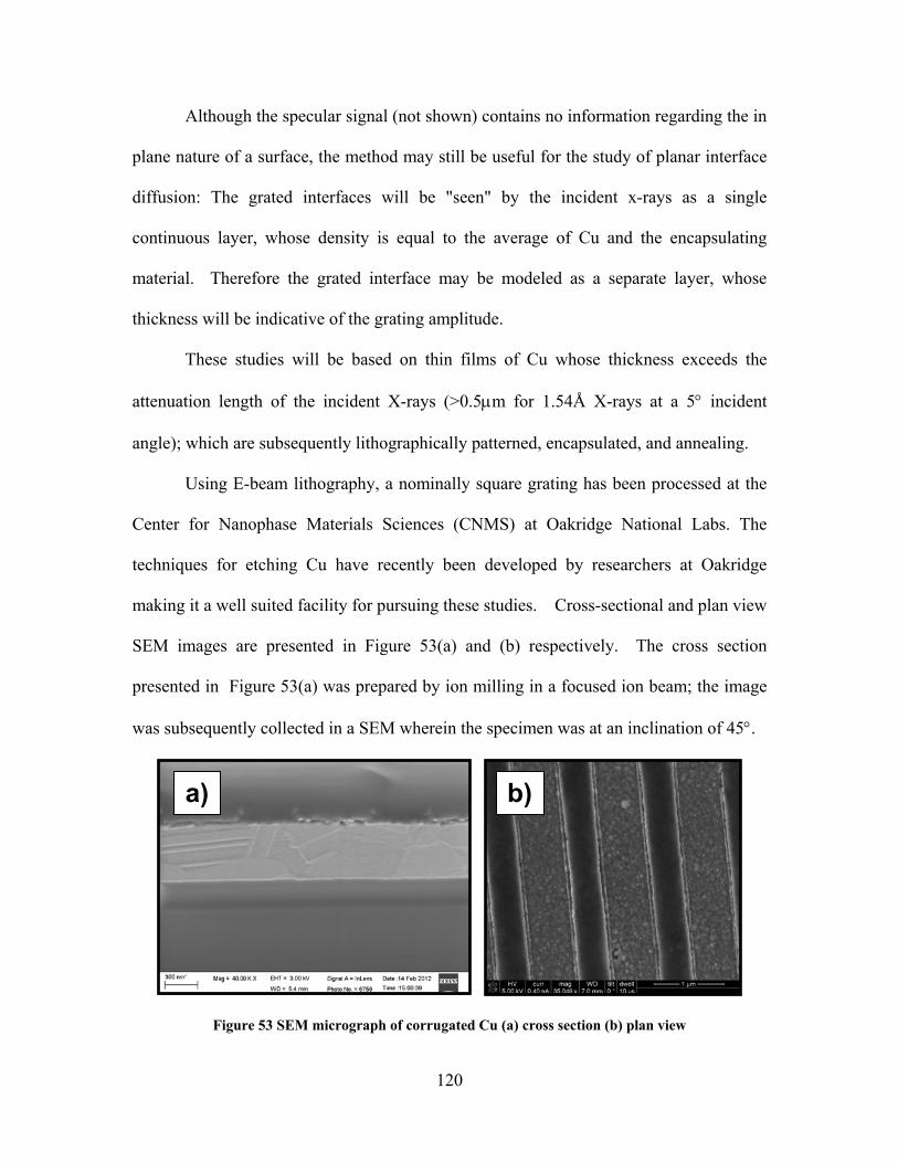
120
Although the specular signal (not shown) contains no information regarding the in
plane nature of a surface, the method may still be useful for the study of planar interface
diffusion: The grated interfaces will be "seen" by the incident x-rays as a single
continuous layer, whose density is equal to the average of Cu and the encapsulating
material. Therefore the grated interface may be modeled as a separate layer, whose
thickness will be indicative of the grating amplitude.
These studies will be based on thin films of Cu whose thickness exceeds the
attenuation length of the incident X-rays (>0.5m for 1.54Å X-rays at a 5 incident
angle); which are subsequently lithographically patterned, encapsulated, and annealing.
Using E-beam lithography, a nominally square grating has been processed at the
Center for Nanophase Materials Sciences (CNMS) at Oakridge National Labs. The
techniques for etching Cu have recently been developed by researchers at Oakridge
making it a well suited facility for pursuing these studies. Cross-sectional and plan view
SEM images are presented in Figure 53(a) and (b) respectively. The cross section
presented in Figure 53(a) was prepared by ion milling in a focused ion beam; the image
was subsequently collected in a SEM wherein the specimen was at an inclination of 45.
Figure 53 SEM micrograph of corrugated Cu (a) cross section (b) plan view
a) b)

121
0 1 2 3 4 5
1E-5
1E-4
1E-3
0.01
0.1
1
No
rmal
ized
In
ten
sity
o
Figure 54 Attempted XRR of corrugated Cu film
First attempts to study these films by x-ray scattering have been unsuccessful
(Figure 54). No measurable oscillations from the grated interface have been detected.
Similarly, no discernable diffuse pattern was detected. The lack of measurable x-ray
scattering patterns may be attributed to the notable roughness along the interface,
superimposed on the grated pattern, resulting from e-beam exposure (Figure 53).
Further development of etching processes is therefore required so that smoother and more
idealized square pulse patterns may be lithographically processed into the Cu surface.

122
REFERENCES
[Aarão Reis 2001] Aarão Reis FDA "Universality and Corrections to Scaling in the Ballistic Deposition Model," Physical Review E, 63 (2001)
[Abrikosov et al. 1993] Abrikosov IA, Skriver HL "Self-Consistent Linear-Muffin-Tin-Orbitals Coherent-Potential Technique for Bulk and Surface Calculations: Cu-Ni, Ag-Pd, and Au-Pt Random Alloys," Physical Review B, 47, 16532 (1993)
[Balluffi et al. 2005] Balluffi RW, Allen SM, Carter WC, Kemper RA, Kinetics of Materials, J. Wiley & Sons, Hoboken, N.J (2005)
[Balogh et al. 2006] Balogh L, Ribaarik G, Ungár T "Stacking Faults and Twin Boundaries in Fcc Crystals Determined by X-Ray Diffraction Profile Analysis," Journal of Applied Physics, 100, 023512 (2006)
[Barabási et al. 1995] Barabási A-L, Stanley EH, Fractal Concepts in Surface Growth, Press Syndicate of the University of Cambridge, New York, NY, USA (1995)
[Birkholz et al. 2006] Birkholz M, Fewster PF, Genzel C, Thin Film Analysis by X-Ray Scattering, John Wiley, Germany, Weinheim (2006)
[Bragg 1913] Bragg WL "The Diffraction of Short Electromagnetic Waves by a Crystal," Proceedings of the Cambridge Philosophical Society, 17, 43 (1913)
[Brune et al. 1995] Brune H, Bromann K, Röder H, Kern K, Jacobsen J, Stoltze P, Jacobsen K, Norskov J "Effect of Strain on Surface Diffusion and Nucleation," Physical Review B, 52, R14380 (1995)
[Castez et al. 2006] Castez M, Salvarezza R, Solari H "Modeling Growth from the Vapor and Thermal Annealing on Micro- and Nanopatterned Substrates," Physical Review E, 73 (2006)
[Choi 2011] Choi D, Tungsten as a Next-Generation Interconnect Metal in Semiconductor Devices, Ph.D., Carnegie Mellon University (2011)
[Choi et al. 2012] Choi D, Kim CS, Naveh D, Chung S, Warren AP, Nuhfer NT, Toney MF, Coffey KR, Barmak K "Electron Mean Free Path of Tungsten and the Electrical Resistivity of Epitaxial (110) Tungsten Films," Physical Review B, 86, 045432 (2012)
[Cullity et al. 2001] Cullity BD, Stock SR, Elements of X-Ray Diffraction, Prentice Hall, Upper Saddle River, NJ (2001)
[De Boer et al. 1996] De Boer DKG, Leenaers AJG "Probing Interface Roughness by X-Ray Scattering," Physica B: Condensed Matter, 221, 18 (1996)

123
[Demir et al. 2009] Demir E, Raabe D, Zaafarani N, Zaefferer S "Investigation of the Indentation Size Effect through the Measurement of the Geometrically Necessary Dislocations beneath Small Indents of Different Depths Using Ebsd Tomography," Acta Materialia, 57, 559 (2009)
[Dubson et al. 1994] Dubson M, Jeffers G "Profile Decay by Surface Diffusion at Low Temperature," Physical Review B, 49, 8347 (1994)
[Edwards et al. 1982] Edwards SF, Wilkinson DR "The Surface Statistics of a Granular Aggregate," Proceedings of the Royal Society A: Mathematical, Physical and Engineering Sciences, 381, 17 (1982)
[El-Dasher et al. 2003] El-Dasher BS, Adams BL, Rollett AD "Viewpoint: Experimental Recovery of Geometrically Necessary Dislocation Density in Polycrystals," Scripta Materialia, 48, 141 (2003)
[Erlebacher et al. 2000] Erlebacher J, Aziz MJ, Chason E, Sinclair MB, Floro JA "Nonclassical Smoothening of Nanoscale Surface Corrugations," Physical Review Letters, 84, 5800 (2000)
[Eshelby 1949] Eshelby JD "Edge Dislocations in Anisotropic Materials " Phil. Mag., 40, 903 (1949)
[Family et al. 1985] Family F, Vicsek T "Scaling of the Active Zone in the Eden Process on Percolation Networks and the Ballistic Deposition Model," Journal of Physics A: Mathematical and General, 18, L75 (1985)
[Gan et al. 2011] Gan D, Ho PS, Pang Y, Huang R, Leu J, Maiz J, Scherban T "Effect of Passivation on Stress Relaxation in Electroplated Copper Films," Journal of Materials Research, 21, 1512 (2011)
[Gao et al. 2003] Gao H, Huang Y "Geometrically Necessary Dislocation and Size-Dependent Plasticity," Scripta Materialia, 48, 113 (2003)
[Gao et al. 2002] Gao H, Zhang L, Baker SP "Dislocation Core Spreading at Interfaces between Metal Films and Amorphous Substrates," Journal of the Mechanics and Physics of Solids, 50, 2169 (2002)
[Geue et al. 2002] Geue T, Henneberg O, Pietsch U "X-Ray Reflectivity from Sinusoidal Surface Relief Gratings," Crystal Research and Technology, 37, 770 (2002)
[Gonçalves et al. 2012] Gonçalves NS, Carvalho JA, Lima ZM, Sasaki JM "Size–Strain Study of Nio Nanoparticles by X-Ray Powder Diffraction Line Broadening," Materials Letters, 72, 36 (2012)
[Gupta 2005] Gupta D, Diffusion Processes in Advanced Technological Materials, William Andrew, Inc., Norwich, N.Y (2005)

124
[Hofmann et al. 2009] Hofmann F, Song X, Dolbnya I, Abbey B, Korsunsky AM "Probing Intra-Granular Deformation by Micro-Beam Laue Diffraction," Procedia Engineering, 1, 193 (2009)
[Holý et al. 1999] Holý V, Baumbach T, Pietsch U, High-Resolution X-Ray Scattering from Thin Films and Multilayers, Springer Tracts in Modern Physics, 0081-3869 ; V. 149, Springer, Berlin ; New York (1999)
[Hughes et al. 1991] Hughes DA, Hansen N "Microstructural Evolution in Nickel During Rolling and Torsion," Materials Science and Technology, 7, 544 (1991)
[Jiran et al. 1990] Jiran E, Thompson C "Capillary Instabilities in Thin Films," Journal of Electronic Materials, 19, 1153 (1990)
[Kardar et al. 1986] Kardar M, Parisi G, Zhang Y-C "Dynamic Scaling of Growing Interfaces," Physical Review Letters, 56, 889 (1986)
[Keblinski et al. 1996] Keblinski P, Maritan A, Toigo F, Messier R, Banavar J "Continuum Model for the Growth of Interfaces," Physical Review E, 53, 759 (1996)
[Khorsand Zak et al. 2012] Khorsand Zak A, Majid WHA, Ebrahimizadeh Abrishami M, Yousefi R, Parvizi R "Synthesis, Magnetic Properties and X-Ray Analysis of Zn0.97x0.03o Nanoparticles (X = mn, Ni, and Co) Using Scherrer and Size–Strain Plot Methods," Solid State Sciences, 14, 488 (2012)
[Kim et al. 2005] Kim T-W, Park S-J, Jones LE, Toney MF, Park K-W, Sung Y-E "Structure and Electrocatalysis of Sputtered Rupt Thin-Film Electrodes," The Journal of Physical Chemistry B, 109, 12845 (2005)
[Korsunsky et al. 2012] Korsunsky AM, Hofmann F, Abbey B, Song X, Belnoue JP, Mocuta C, Dolbnya I "Analysis of the Internal Structure and Lattice (Mis)Orientation in Individual Grains of Deformed Cp Nickel Polycrystals by Synchrotron X-Ray Micro-Diffraction and Microscopy," International Journal of Fatigue, 42, 1 (2012)
[Lanckmans et al. 2002] Lanckmans F, Brongersma SH, Varga I, Poortmans S, Bender H, Conard T, Maex K "A Quantitative Adhesion Study between Contacting Materials in Cu Damascene Structures," Applied Surface Science, 201, 20 (2002)
[Lane et al. 2003] Lane MW, Liniger EG, Lloyd JR "Relationship between Interfacial Adhesion and Electromigration in Cu Metallization," Journal of Applied Physics, 93, 1417 (2003)
[Langford et al. 1988] Langford JI, Delhez R, Keijser THD, Mittemeijer EJ "Profile Analysis for Microcrystalline Properties by the Fourier and Other Methods," Aust. J. Phys., 41, 173 (1988)

125
[Langford et al. 1978] Langford JI, Wilson AJC "Scherrer after Sixty Years: A Survey and Some New Results in the Determination of Crystallite Size," Journal of Applied Crystallography, 11, 102 (1978)
[Larche et al. 1982] Larche FC, Cahn JL "The Effect of Self-Stress on Diffusion in Solids," Acta Metallurgica, 30, 1835 (1982)
[Laue 1913] Laue MV "Röntgenstrahlinterferenzen," Physikalische Zeitschrift, 14, 1075 (1913)
[Lita et al. 2000] Lita AE, Sanchez JE, Jr. "Effects of Grain Growth on Dynamic Surface Scaling During the Deposition of Al Polycrystalline Thin Films," Physical Review B, 61, 7692 (2000)
[Maiya et al. 1965] Maiya PS, Blakely JM "A Technique for Study of Mass Transport Mechanisms at Crystal Surfaces," Applied Physics Letters, 7, 60 (1965)
[Mandelbrot 1985] Mandelbrot BB "Self-Affine Fractals and Fractal Dimension," Physica Scripta, 32, 257 (1985)
[Massalski et al. 1990] Massalski TB, Okamoto H, Binary Alloy Phase Diagrams / Editor-in-Chief, Thaddeus B. Massalski ; Editors, Hiroaki Okamoto, P.R. Subramanian, Linda Kacprzak ; Publisher, William W. Scott, Jr, Materials Park, Ohio : ASM International (1990)
[Meakin 1998] Meakin P, Fractals, Scaling, and Growth Far from Equilibrium, Cambridge Nonlinear Science Series ; 5, Cambridge University Press, Cambridge, U.K. ; New York (1998)
[Müllner et al. 1998] Müllner P, Arzt E "Observation of Dislocations Disappearance in Aluminum Thin Films and Consequences for Thin Film Properties" Mater. Res. Soc. Symp. Proc., 505, 149 (1998)
[Nichols et al. 1965] Nichols FA, Mullins WW "Morphological Changes of a Surface of Revolution Due to Capillarity-Induced Surface Diffusion," Journal of Applied Physics, 36, 1826 (1965)
[Nye 1953] Nye JF "Some Geometrical Relations in Dislocated Solids," Acta Metallurgica, 1, 153 (1953)
[Ogilvy et al. 1989] Ogilvy JA, Foster JR "Rough Surfaces: Gaussian or Exponential Statistics?," Journal of Physics D: Applied Physics, 22, 1243 (1989)
[Overton et al. 1955] Overton W, Gaffney J "Temperature Variation of the Elastic Constants of Cubic Elements. I. Copper," Physical Review, 98, 969 (1955)
[Parratt 1954] Parratt LG "Surface Studies of Solids by Total Reflection of X-Rays," Physical Review, 95, 359 (1954)

126
[Pelliccione et al. 2008] Pelliccione M, Lu TM, Evolution of Thin-Film Morphology Modeling and Simulations, Springer Series in Materials Science ; V. 108. 0933-033x, Springer, Berlin ; New York (2008)
[Rabkin 2012] Rabkin E "Flattening of a Passivated Solid Surface Due to Capillarity," Scripta Materialia, 67, 625 (2012)
[Read et al. 1950] Read WT, Shockley W "Dislocation Models of Crystal Grain Boundaries," Physical Review, 78, 275 (1950)
[Révész et al. 1996] Révész Á, Ungár T, Borbély A, Lendvai J "Dislocations and Grain Size in Ball-Milled Iron Powder," Nanostructured Materials, 7, 779 (1996)
[Savaloni et al. 2006] Savaloni H, Gholipour-Shahraki M, Player MA "A Comparison of Different Methods for X-Ray Diffraction Line Broadening Analysis of Ti and Ag Uhv Deposited Thin Films: Nanostructural Dependence on Substrate Temperature and Film Thickness," Journal of Physics D: Applied Physics, 39, 2231 (2006)
[Scherrer 1918] Scherrer P "Bestimmung Der Größe Und Der Inneren Struktur Von Kolloidteilchen Mittels Röntgenstrahlen," Nachrichten von der Königlichen Gesellschaft der Wissenschaften zu Göttingen, Mathematisch-physikalische Klasse (1918)
[Schlatmann et al. 1996] Schlatmann R, Shindler JD, Verhoeven J "Evolution of Surface Morphology During Growth and Ion Erosion of Thin Films," Physical Review B, 54, 10880 (1996)
[Schmidbauer 2003] Schmidbauer M, X-Ray Diffuse Scattering from Self-Organized Mesoscopic Semiconductor Structures, Springer Tracts in Modern Physics, 0081-3869 ; V. 199, Springer, Berlin ; New York (2003)
[Shu et al. 2001] Shu D, Liu F, Gong X "Simple Generic Method for Predicting the Effect of Strain on Surface Diffusion," Physical Review B, 64 (2001)
[Sinha et al. 1988] Sinha SK, Sirota EB, Garoff S "X-Ray and Neutron Scattering from Rough Surfaces," Physical Review B, 38, 2297 (1988)
[Smilgies 2009] Smilgies DM "Scherrer Grain-Size Analysis Adapted to Grazing-Incidence Scattering with Area Detectors," J Appl Crystallogr, 42, 1030 (2009)
[Stokes et al. 1944] Stokes AR, Wilson AJC "The Diffraction of X Rays by Distorted Crystal Aggregates - I," Proceedings of the Physical Society, 56, 174 (1944)
[Sun 2009] Sun T, Classical Size Effect in Copper Thin Films: Impact of Surface and Grain Boundary Scattering on Resistivity, Ph.D., University of Central Florida (2009)
[Sun et al. 2009] Sun T, Yao B, Warren A, Barmak K, Toney M, Peale R, Coffey K "Dominant Role of Grain Boundary Scattering in the Resistivity of Nanometric Cu Films," Physical Review B, 79 (2009)

127
[Sun et al. 2010] Sun T, Yao B, Warren AP, Barmak K, Toney MF, Peale RE, Coffey KR "Surface and Grain-Boundary Scattering in Nanometric Cu Films," Physical Review B, 81 (2010)
[Sun et al. 2008] Sun T, Yao B, Warren AP, Kumar V, Roberts S, Barmak K, Coffey KR "Classical Size Effect in Oxide-Encapsulated Cu Thin Films: Impact of Grain Boundaries Versus Surfaces on Resistivity," Journal of Vacuum Science & Technology A: Vacuum, Surfaces, and Films, 26, 605 (2008)
[Todi et al. 2007] Todi RM, Erickson MS, Sundaram KB, Barmak K, Coffey KR "Comparison of the Work Function of Pt&Ndash;Ru Binary Metal Alloys Extracted from Mos Capacitor and Schottky-Barrier-Diode Measurements," Electron Devices, IEEE Transactions on, 54, 807 (2007)
[Todi et al. 2006] Todi RM, Warren AP, Sundaram KB, Barmak K, Coffey KR "Characterization of Pt-Ru Binary Alloy Thin Films for Work Function Tuning," Electron Device Letters, IEEE, 27, 542 (2006)
[Tolan 1998] Tolan M, X-Ray Scattering from Soft-Matter Thin Films : Materials Science and Basic Research, Springer Tracts in Modern Physics ; 148, Springer, New York (1998)
[Ungár 1996] Ungár T "Strain Broadening Caused by Dislocations," Advances in X-ray Analysis, 40 (1996)
[Ungár 2008] Ungár T "Dislocation Model of Strain Anisotropy," Powder Diffraction, 23, 125 (2008)
[Ungár et al. 1996] Ungár T, Borbely A "The Effect of Dislocation Contrast on X-Ray Line Broadening: A New Approach to Line Profile Analysis," Applied Physics Letters, 69, 3173 (1996)
[Ungár et al. 1999] Ungár T, Dragomir I, Revesz A, Borbely A "The Contrast Factors of Dislocations in Cubic Crystals: The Dislocation Model of Strain Anisotropy in Practice," Journal of Applied Crystallography, 32, 992 (1999)
[Ungár et al. 2012] Ungár T, Tichy G, Gubicza J, Hellmig RJ "Correlation between Subgrains and Coherently Scattering Domains," Powder Diffraction, 20, 366 (2012)
[Vidal et al. 1984] Vidal B, Vincent P "Metallic Multilayers for X Rays Using Classical Thin-Film Theory," Appl. Opt., 23, 1794 (1984)
[Vvedensky 2003] Vvedensky D "Edwards-Wilkinson Equation from Lattice Transition Rules," Physical Review E, 67 (2003)
[Wang et al. 2011] Wang J, Misra A "An Overview of Interface-Dominated Deformation Mechanisms in Metallic Multilayers," Current Opinion in Solid State and Materials Science, 15, 20 (2011)

128
[Warren et al. 2008] Warren AP, Todi RM, Yao B, Barmak K, Sundaram KB, Coffey KR "On the Phase Identification of Dc Magnetron Sputtered Pt–Ru Alloy Thin Films," Journal of Vacuum Science & Technology A: Vacuum, Surfaces, and Films, 26, 1208 (2008)
[Warren 1990] Warren BE, X-Ray Diffraction, Dover Publications, New York (1990)
[Wilk et al. 2001] Wilk GD, Wallace RM, Anthony JM "High-Κ Gate Dielectrics: Current Status and Materials Properties Considerations," Journal of Applied Physics, 89, 5243 (2001)
[Wilkens 1970] Wilkens M "The Determination of Density and Distribution of Dislocations in Deformed Single Crystals from Broadened X-Ray Diffraction Profiles," physica status solidi (a), 2, 359 (1970)
[Wilkens et al. 1987] Wilkens M, Ungár T, Mughrabi H "X-Ray Rocking-Curve Broadening of Tensile-Deformed 001 -Orientated Copper Single-Crystals," Physica Status Solidi a-Applied Research, 104, 157 (1987)
[Williamson et al. 1953] Williamson GK, Hall WH "X-Ray Line Broadening from Filed Aluminium and Wolfram," Acta Metallurgica, 1, 22 (1953)
[Wormington et al. 1999] Wormington M, Panaccione C, Matney KM, Bowen KD "Characterization of Structures from X-Ray Scattering Data Using Genetic Algorithms," Philosophical Transactions of the Royal Society of London. Series A: Mathematical, Physical and Engineering Sciences, 357, 2827 (1999)
[Yao et al. 2008] Yao B, Coffey KR "Back-Etch Method for Plan View Transmission Electron Microscopy Sample Preparation of Optically Opaque Films," Journal of Electron Microscopy, 57, 47 (2008)
[Yao et al. 2008] Yao B, Coffey KR "A High-Throughput Approach for Cross-Sectional Transmission Electron Microscopy Sample Preparation of Thin Films," J Electron Microsc (Tokyo), 57, 189 (2008)