
WM8990 Product Brief · 2016-12-16 · Active noise reduction - DC offset correction removes pops...
221
Audio Hub Codec for Multimedia Phones http://www.cirrus.com Copyright Cirrus Logic, Inc., 2008–2016 (All Rights Reserved) Rev 4.1 NOV ‘16 WM8993 DESCRIPTION The WM8993 is a highly integrated ultra-low power hi-fi CODEC designed for portable devices such as multimedia phones. A stereo 1W/channel speaker driver can operate in class D or AB mode. Low leakage and high PSRR across the audio band enable direct battery connection for the speaker supply. Class W headphone drivers provide a dramatic reduction in playback power and are ground-referenced. Active ground loop noise rejection and DC offset correction help prevent pop noise and ground noise from degrading headphone output quality. Powerful mixing capability allows the device to support a huge range of architectures and use cases. A highly flexible input configuration supports multiple microphone or line inputs (mono or stereo, single-ended or differential). Fully differential internal architecture and on-chip RF noise filters ensure a very high degree of noise immunity. ReTune TM Mobile parametric EQ with fully programmable coefficients is integrated for optimization of speaker characteristics. Programmable dynamic range control is also available for maximizing loudness, protecting speakers from clipping and preventing premature shutdown due to battery droop. The WM8993 is supplied in very small and thin 48-ball W-CSP package, ideal for portable systems. FEATURES 100dB SNR during DAC playback (‘A’ weighted) Low power, low noise MIC interface Class D or AB stereo speaker driver - Stereo1W into 8 BTL speaker at <1% THD - Mono 2W into 4 BTL speaker ReTune Mobile parametric equalizer Dynamic range controller Low power Class W headphone drivers - Integrated charge pump and DC offset correction - 5mW total power for DAC playback to headphones Digital audio interface - All standard data formats and 2-channel TDM supported - All standard sample rates from 8kHz to 48kHz Low power FLL - Provides all necessary internal clocks - 32kHz to 27MHz input frequency - Free-running mode for class D and charge pump 4 highly flexible line outputs (single-ended or differential ) Dedicated earpiece driver “Direct voice” and “Direct DAC” paths to outputs - Low noise paths bypass all internal mixers - Low power consumption Active noise reduction - DC offset correction removes pops and clicks - Ground loop noise cancellation 48-ball W-CSP package (3.65x3.55x0.546mm, 0.5mm pitch) APPLICATIONS Multimedia phones LINE DRIVERS LOUDSPEAKER DRIVERS CONTROL INTERFACE SDAT SCLK MICBIAS1 HPOUT2P HPOUT1R ADCDAT BCLK GPIO1 DACDAT LRCLK IN1LP IN1LN IN1RN HPOUT2N IN2LN IN2RN IN1RP LINEOUT1P LINEOUT1N HPOUT1L SPKOUTLP SPKOUTLN IN2RP/VRXP IN2LP/VRXN RECORD HEADPHONE DRIVERS Current Detect RECORD CPFB2 CPFB1 CHARGE PUMP CPVOUTP CPVOUTN AUDIO CLOCKS MIC INTERFACE INPUT MIXERS DIGITAL AUDIO INTERFACE ADC FILTERS HIGH PASS FILTERS ADC VOLUME DAC FILTERS DAC VOLUME DAC L DAC R ADC L ADC R AVDD1 VMIDC AGND1 DCVDD DBVDD DGND SPKVDD SPKGND CPVDD CPGND ReTune TM Mobile PARAMETRIC EQUALISER DYNAMIC RANGE CONTROL GPIO HPOUT1FB EARPIECE DRIVER SPKOUTRP SPKOUTRN OUTPUT MIXERS AVDD2 FLL LINEOUT2P LINEOUT2N LINEOUTFB MCLK SPKMONO MICBIAS2 Current Detect GPIO GPIO
Transcript of WM8990 Product Brief · 2016-12-16 · Active noise reduction - DC offset correction removes pops...

Audio Hub Codec for Multimedia Phones
http://www.cirrus.com
Copyright Cirrus Logic, Inc., 2008–2016
(All Rights Reserved)
Rev 4.1
NOV ‘16
WM8993
DESCRIPTION
The WM8993 is a highly integrated ultra-low power hi-fi CODEC
designed for portable devices such as multimedia phones.
A stereo 1W/channel speaker driver can operate in class D or
AB mode. Low leakage and high PSRR across the audio band
enable direct battery connection for the speaker supply.
Class W headphone drivers provide a dramatic reduction in
playback power and are ground-referenced. Active ground loop
noise rejection and DC offset correction help prevent pop noise
and ground noise from degrading headphone output quality.
Powerful mixing capability allows the device to support a huge
range of architectures and use cases. A highly flexible input
configuration supports multiple microphone or line inputs (mono
or stereo, single-ended or differential).
Fully differential internal architecture and on-chip RF noise filters
ensure a very high degree of noise immunity.
ReTuneTM Mobile parametric EQ with fully programmable
coefficients is integrated for optimization of speaker
characteristics. Programmable dynamic range control is also
available for maximizing loudness, protecting speakers from
clipping and preventing premature shutdown due to battery
droop.
The WM8993 is supplied in very small and thin 48-ball W-CSP
package, ideal for portable systems.
FEATURES
100dB SNR during DAC playback (‘A’ weighted)
Low power, low noise MIC interface
Class D or AB stereo speaker driver
- Stereo1W into 8 BTL speaker at <1% THD
- Mono 2W into 4 BTL speaker
ReTune Mobile parametric equalizer
Dynamic range controller
Low power Class W headphone drivers
- Integrated charge pump and DC offset correction
- 5mW total power for DAC playback to headphones
Digital audio interface
- All standard data formats and 2-channel TDM supported
- All standard sample rates from 8kHz to 48kHz
Low power FLL
- Provides all necessary internal clocks
- 32kHz to 27MHz input frequency
- Free-running mode for class D and charge pump
4 highly flexible line outputs (single-ended or differential )
Dedicated earpiece driver
“Direct voice” and “Direct DAC” paths to outputs
- Low noise paths bypass all internal mixers
- Low power consumption
Active noise reduction
- DC offset correction removes pops and clicks
- Ground loop noise cancellation
48-ball W-CSP package (3.65x3.55x0.546mm, 0.5mm pitch)
APPLICATIONS
Multimedia phones
LINE DRIVERS
LOUDSPEAKER
DRIVERS
CONTROL
INTERFACE
SD
AT
SC
LK
MICBIAS1
HPOUT2P
HPOUT1R
AD
CD
AT
BC
LK
GP
IO1
DA
CD
AT
LR
CL
K
IN1LPIN1LN
IN1RN
HPOUT2N
IN2LN
IN2RNIN1RP
LINEOUT1P
LINEOUT1N
HPOUT1L
SPKOUTLPSPKOUTLN
IN2RP/VRXP
IN2LP/VRXN
RECORD
HEADPHONE
DRIVERS
Current
Detect
RECORD
CPFB2
CPFB1CHARGE PUMP
CPVOUTP CPVOUTN
AUDIO
CLOCKS
MIC
INTERFACE
INPUT
MIXERS
DIGITAL AUDIO
INTERFACE
ADC
FILTERS
HIGH
PASS
FILTERS
ADC
VOLUME
DAC
FILTERS
DAC
VOLUME
DAC L
DAC R
ADC L
ADC R
AVDD1 VMIDC AGND1 DCVDD DBVDD DGND SPKVDD SPKGND CPVDD CPGND
ReTuneTM
Mobile
PARAMETRIC EQUALISER
DYNAMIC RANGE CONTROL
GPIO
HPOUT1FB
EARPIECE
DRIVER
SPKOUTRPSPKOUTRN
OUTPUT
MIXERS
AVDD2
FLL
LINEOUT2P
LINEOUT2N
LINEOUTFB
MC
LK
SPKMONO
MICBIAS2Current
DetectGPIO
GPIO

WM8993
Rev 4.1 2
TABLE OF CONTENTS
DESCRIPTION ...................................................................................................... 1
FEATURES ........................................................................................................... 1
APPLICATIONS .................................................................................................... 1
TABLE OF CONTENTS ........................................................................................ 2
BLOCK DIAGRAM ............................................................................................... 5
PIN CONFIGURATION ......................................................................................... 6
ORDERING INFORMATION ................................................................................. 6
PIN DESCRIPTION ............................................................................................... 6
ABSOLUTE MAXIMUM RATINGS ....................................................................... 8
RECOMMENDED OPERATING CONDITIONS .................................................... 8
THERMAL PERFORMANCE ................................................................................ 9
ELECTRICAL CHARACTERISTICS .................................................................. 10 TERMINOLOGY ........................................................................................................... 23
TYPICAL PERFORMANCE ................................................................................ 24 POWER CONSUMPTION ............................................................................................ 24
AUDIO SIGNAL PATHS DIAGRAM ................................................................... 25
SIGNAL TIMING REQUIREMENTS ................................................................... 26 MASTER CLOCK ......................................................................................................... 26 AUDIO INTERFACE TIMING ....................................................................................... 27
MASTER MODE ............................................................................................................................................................ 27 SLAVE MODE ................................................................................................................................................................ 28 TDM MODE ................................................................................................................................................................... 29
CONTROL INTERFACE TIMING ................................................................................. 30
DEVICE DESCRIPTION ..................................................................................... 31 INTRODUCTION .......................................................................................................... 31 INPUT SIGNAL PATH .................................................................................................. 33
MICROPHONE INPUTS ................................................................................................................................................ 34 MICROPHONE BIAS CONTROL .................................................................................................................................. 34 MICROPHONE CURRENT DETECT ............................................................................................................................ 35 LINE AND VOICE CODEC INPUTS .............................................................................................................................. 35 INPUT PGA ENABLE .................................................................................................................................................... 36 INPUT PGA CONFIGURATION .................................................................................................................................... 37 INPUT PGA VOLUME CONTROL ................................................................................................................................. 38 INPUT MIXER ENABLE ................................................................................................................................................. 40 INPUT MIXER CONFIGURATION AND VOLUME CONTROL ..................................................................................... 40
ANALOGUE TO DIGITAL CONVERTER (ADC) .......................................................... 43 ADC DIGITAL VOLUME CONTROL .............................................................................................................................. 43 HIGH PASS FILTER ...................................................................................................................................................... 45
DIGITAL MIXING .......................................................................................................... 46 DIGITAL MIXING PATHS .............................................................................................................................................. 46 DAC INTERFACE VOLUME BOOST ............................................................................................................................ 48 DIGITAL SIDETONE ...................................................................................................................................................... 48
DYNAMIC RANGE CONTROL (DRC) ......................................................................... 49 COMPRESSION/LIMITING CAPABILITIES .................................................................................................................. 49 GAIN LIMITS .................................................................................................................................................................. 51 DYNAMIC CHARACTERISTICS ................................................................................................................................... 52 ANTI-CLIP CONTROL ................................................................................................................................................... 52 QUICK RELEASE CONTROL ....................................................................................................................................... 53 GAIN SMOOTHING ....................................................................................................................................................... 53 INITIALISATION ............................................................................................................................................................ 54

WM8993
Rev 4.1 3
RETUNE MOBILE PARAMETRIC EQUALIZER (EQ) .................................................. 55 DEFAULT MODE (5-BAND PARAMETRIC EQ) ........................................................................................................... 55 RETUNE MOBILE MODE .............................................................................................................................................. 56 EQ FILTER CHARACTERISTICS ................................................................................................................................. 56
DIGITAL TO ANALOGUE CONVERTER (DAC) .......................................................... 58 DAC DIGITAL VOLUME CONTROL .............................................................................................................................. 58 DAC SOFT MUTE AND SOFT UN-MUTE ..................................................................................................................... 60 DAC MONO MIX ............................................................................................................................................................ 61 DAC DE-EMPHASIS ...................................................................................................................................................... 61 DAC SLOPING STOPBAND FILTER ............................................................................................................................ 62
OUTPUT SIGNAL PATH .............................................................................................. 63 OUTPUT SIGNAL PATHS ENABLE .............................................................................................................................. 64 HEADPHONE SIGNAL PATHS ENABLE ...................................................................................................................... 65 OUTPUT MIXER CONTROL ......................................................................................................................................... 67 SPEAKER MIXER CONTROL ....................................................................................................................................... 70 OUTPUT SIGNAL PATH VOLUME CONTROL ............................................................................................................. 71 SPEAKER BOOST MIXER ............................................................................................................................................ 76 EARPIECE DRIVER MIXER .......................................................................................................................................... 77 LINE OUTPUT MIXERS ................................................................................................................................................ 77
CHARGE PUMP ........................................................................................................... 81 DC SERVO ................................................................................................................... 83
DC SERVO ENABLE AND START-UP ......................................................................................................................... 83 DC SERVO ACTIVE MODES ........................................................................................................................................ 85 DC SERVO READBACK ............................................................................................................................................... 86
ANALOGUE OUTPUTS ............................................................................................... 87 SPEAKER OUTPUT CONFIGURATIONS ..................................................................................................................... 87 HEADPHONE OUTPUT CONFIGURATIONS ............................................................................................................... 90 EARPIECE DRIVER OUTPUT CONFIGURATIONS ..................................................................................................... 91 LINE OUTPUT CONFIGURATIONS .............................................................................................................................. 91
GENERAL PURPOSE INPUT/OUTPUT ...................................................................... 94 GPIO1 CONTROL ......................................................................................................................................................... 94 BUTTON DETECT ......................................................................................................................................................... 95 ACCESSORY DETECTION ........................................................................................................................................... 96 CLOCK OUTPUT ........................................................................................................................................................... 99 FLL LOCK STATUS OUTPUT ....................................................................................................................................... 99 TEMPERATURE SENSOR OUTPUT .......................................................................................................................... 100 CONTROL WRITE SEQUENCER STATUS ................................................................................................................ 101 LOGIC ‘1’ AND LOGIC ‘0’ OUTPUT ............................................................................................................................ 102 INTERRUPTS .............................................................................................................................................................. 102 GPIO SUMMARY ......................................................................................................................................................... 103
DIGITAL AUDIO INTERFACE .................................................................................... 105 MASTER AND SLAVE MODE OPERATION ............................................................................................................... 105 OPERATION WITH TDM ............................................................................................................................................. 106 BCLK FREQUENCY .................................................................................................................................................... 107 AUDIO DATA FORMATS (NORMAL MODE) .............................................................................................................. 107 AUDIO DATA FORMATS (TDM MODE) ..................................................................................................................... 109
DIGITAL AUDIO INTERFACE CONTROL ................................................................. 111 AUDIO INTERFACE OUTPUT TRI-STATE ................................................................................................................. 112 BCLK AND LRCLK CONTROL .................................................................................................................................... 112 COMPANDING ............................................................................................................................................................ 114 LOOPBACK ................................................................................................................................................................. 116 DIGITAL PULL-UP AND PULL-DOWN ........................................................................................................................ 116
CLOCKING AND SAMPLE RATES ............................................................................ 117 CLK_SYS CONTROL .................................................................................................................................................. 119 AUTOMATIC CLOCKING CONFIGURATION ............................................................................................................. 120

WM8993
Rev 4.1 4
ADC / DAC CLOCK CONTROL ................................................................................................................................... 121 256K, DC SERVO, CLASS D CLOCK CONTROL ...................................................................................................... 122 OPCLK CONTROL ...................................................................................................................................................... 123 TOCLK CONTROL ...................................................................................................................................................... 124 BCLK AND LRCLK CONTROL .................................................................................................................................... 124 FREQUENCY LOCKED LOOP (FLL) .......................................................................................................................... 125 FREE-RUNNING FLL CLOCK ..................................................................................................................................... 128 EXAMPLE FLL CALCULATION ................................................................................................................................... 128 EXAMPLE FLL SETTINGS .......................................................................................................................................... 129
CONTROL INTERFACE ............................................................................................. 130 CONTROL WRITE SEQUENCER .............................................................................. 133
INITIATING A SEQUENCE .......................................................................................................................................... 133 PROGRAMMING A SEQUENCE ................................................................................................................................ 134 DEFAULT SEQUENCES ............................................................................................................................................. 136
POP SUPPRESSION CONTROL .............................................................................. 143 DISABLED LINE OUTPUT CONTROL ........................................................................................................................ 143 LINE OUTPUT DISCHARGE CONTROL .................................................................................................................... 144 VMID REFERENCE DISCHARGE CONTROL ............................................................................................................ 144 INPUT VMID CLAMPS ................................................................................................................................................ 144
REFERENCE VOLTAGES AND MASTER BIAS ....................................................... 145 POWER MANAGEMENT ........................................................................................... 146 POWER ON RESET................................................................................................... 150 QUICK START-UP AND SHUTDOWN ...................................................................... 152 SOFTWARE RESET AND DEVICE ID ....................................................................... 153 THERMAL SHUTDOWN ............................................................................................ 153
REGISTER MAP ............................................................................................... 154 REGISTER BITS BY ADDRESS ................................................................................ 159
DIGITAL FILTER CHARACTERISTICS ........................................................... 205 ADC FILTER RESPONSES ....................................................................................... 206 ADC HIGH PASS FILTER RESPONSES ................................................................... 206 DAC FILTER RESPONSES ....................................................................................... 207 DE-EMPHASIS FILTER RESPONSES ...................................................................... 208
APPLICATIONS INFORMATION ..................................................................... 209 RECOMMENDED EXTERNAL COMPONENTS ........................................................ 209
AUDIO INPUT PATHS ................................................................................................................................................. 209 HEADPHONE OUTPUT PATH .................................................................................................................................... 211 EARPIECE DRIVER OUTPUT PATH .......................................................................................................................... 211 LINE OUTPUT PATHS ................................................................................................................................................ 211 POWER SUPPLY DECOUPLING ............................................................................................................................... 212 CHARGE PUMP COMPONENTS ............................................................................................................................... 213 MICROPHONE BIAS CIRCUIT ................................................................................................................................... 213 CLASS D SPEAKER CONNECTIONS ........................................................................................................................ 214 RECOMMENDED EXTERNAL COMPONENTS DIAGRAM ....................................................................................... 216
PCB LAYOUT CONSIDERATIONS ........................................................................... 218 CLASS D LOUDSPEAKER CONNECTION ................................................................................................................ 218
PACKAGE DIMENSIONS ................................................................................. 219
IMPORTANT NOTICE ...................................................................................... 220
REVISION HISTORY ........................................................................................ 221

WM8993
Rev 4.1 5
BLOCK DIAGRAM
CO
NT
RO
L
INT
ER
FA
CE
SDATSCLK
ADCDAT
BCLK
DACDATLRCLK
CPVDD
CPGND
MIC
BIA
S2
AVDD1
AGND
VMIDC
IN1LP
IN1LN
IN1R
N
IN2LN
/GI7
IN2R
N/G
I8
IN1R
P
IN2LP
/VR
XN
IN2R
P/V
RX
P
MIX
INR
IN1
L
IN2
L
IN2
R
IN1
R
RX
VO
ICE
MIX
INL
CP
FB
1C
PF
B2
CP
VO
UT
NC
PV
OU
TP
+- +- +- +-
+-
LIN
EO
UT
1N
LIN
EO
UT
1P
HP
OU
T1
L
HP
OU
T1
R
HP
OU
T2
N
IN1R
IN1
L
MIX
INR
MIX
INL
RE
C L
RE
C R
HPOUT1FB
CH
AR
GE
PU
MP
RE
C L
RE
C R
DA
C L
DA
C R
AD
C L
DA
CL
Vol
DA
CR
Vol
AD
C R
DC
VD
DD
BV
DD
DG
ND
SP
KG
ND
SP
KV
DD
AD
CL
Vol
AD
CR
Vol
Re
Tu
ne
Mo
bil
e
Pa
ram
etr
ic
Eq
ua
lize
r
Gro
und L
oop N
ois
e R
eje
ction
L R
R L
L/R
SW
AP
AV
DD
2
Gain
Co
des
V =
Full
volu
me c
ontr
ol
(-
71
.625
dB
to 0
dB
, 0
.375dB
ste
ps for
DA
C
-
71
.62
5dB
to
17.6
25d
B, 0
.375dB
ste
ps for
AD
C/M
ICs)
S =
So
ftm
ute
/un
-mute
G =
Fix
ed g
ain
contr
ol
(-
36
dB
to 0
dB
, 3dB
ste
ps)
[Co
de]
Dyn
am
ic R
an
ge
Co
nto
ller
HP
OU
T2
P
DC
Offset C
orr
ection
SP
KO
UT
LP
SP
KO
UT
LN
RE
FE
RE
NC
E
GE
NE
RA
TO
R
+ ++ +
Dire
ct V
oic
e
SP
KO
UT
RP
SP
KO
UT
RN
Dire
ct V
oic
e
Dire
ct V
oic
e
+ +++
IN1LP
IN1LN
IN1
RN
IN2
LN
/GI7
IN2
RN
/GI8
IN1
RP
IN2
LP
/VR
XN
IN2R
P/V
RX
P
SP
KM
IXL
SP
KM
IXR
MIX
OU
TL
MIX
OU
TR
LIN
EO
UT
1N
MIX
LIN
EO
UT
1P
MIX
HP
OU
T2
MIX
Head
phone
Gro
und L
oop
Nois
e R
eje
ction
Feedba
ck
SP
KO
UT
LB
OO
ST
SP
KO
UT
RB
OO
STG
round L
oop N
ois
e R
eje
ction
DC
Offset C
orr
ection
-16
.5d
B m
in
+3
0dB
max
1.5
dB
ste
p
-16
.5d
B m
in
+3
0dB
max
1.5
dB
ste
p
-16
.5d
B m
in
+3
0dB
max
1.5
dB
ste
p
-16
.5d
B m
in
+3
0dB
max
1.5
dB
ste
p
-12
dB
to +
6dB
, 3
dB
ste
p
0dB
or
+3
0dB
MIX
OU
TL
VO
L
HP
OU
T1
LV
OL
SP
KL
VO
L
MIX
OU
TR
VO
L
HP
OU
T1
RV
OL
Min
= -
57dB
Max =
+6
dB
Ste
p =
1d
B
Min
= -
57
dB
Max =
+6dB
Ste
p =
1d
B
Min
= -
57dB
Max =
+6
dB
Ste
p =
1dB
Min
= -
57dB
Max =
+6
dB
Ste
p =
1dB
Min
= -
57
dB
Max =
+6
dB
Ste
p =
1d
B
Min
= -
57dB
Max =
+6
dB
Ste
p =
1dB
SP
KR
VO
L
0dB
or
+3
0dB
-12
dB
to +
6dB
, 3
dB
ste
p
0dB
or
+3
0dB
0dB
or
+3
0dB
-12dB
to +
6d
B,
3dB
ste
p
-12dB
to +
6d
B,
3dB
ste
p
-12dB
to +
6d
B, 3
dB
ste
p
-21dB
to 0
dB
, 3dB
ste
p
-21
dB
to 0
dB
, 3
dB
ste
p
-21
dB
to 0
dB
, 3
dB
ste
p
-21
dB
to 0
dB
, 3
dB
ste
p
0dB
to +
12
dB
, 1.5
dB
ste
p
0d
B to
+1
2dB
, 1.5
dB
ste
p
0dB
or
-6d
B
0dB
or
-6d
B
0dB
or
-6d
B
Dire
ct D
AC
L
Dire
ct D
AC
R
-12
dB
to +
6dB
, 3
dB
ste
p
++
LIN
EO
UT
2N
LIN
EO
UT
2P
+
LIN
EO
UT
2N
MIX
LIN
EO
UT
2P
MIX
0dB
or
-6d
B
0dB
or
-6d
B
LINEOUTFB
Lin
e O
utp
ut
Gro
und L
oop
Nois
e R
eje
ction
Feedba
ck
SPKMONO
Speake
r M
ono /
Ste
reo M
ode
Sele
ct
GPIO1
MIC
BIA
S1
MIC
BIA
S
Curr
ent
Dete
ct
MIC
BIA
S
Curr
ent
Dete
ct
GP
IO
GP
IO
Dyn
am
ic R
an
ge
Co
nto
ller
+ +
+
DIG
ITA
L A
UD
IO
INT
ER
FA
CE
A-l
aw
an
d
-la
w S
up
po
rt
TD
M S
up
po
rt
VV
VS
MO
NO
MIX
VS
+
G G
L R
R L
Gro
und L
oop
Nois
e R
eje
ction
Gro
und L
oop
Nois
e R
eje
ction
Gro
und L
oop
Nois
e R
eje
ction
Gro
und L
oop
Nois
e R
eje
ction
Dyn
am
ic R
an
ge
Co
ntr
ol
(DR
C)
ava
ilab
le o
n A
DC
or
DA
C c
ha
nn
els
, n
ot
bo
th.
+ +
Dir
ec
t V
oic
e
GPIO1
CL
K_
SY
SF
LL
MCLK
GP
IO
BC
LK
LR
CL
K

WM8993
Rev 4.1 6
PIN CONFIGURATION
A
B
C
D
E
F
G
1 2 3 4 5 6 7
DBVDD DCVDD
MCLK
LRCLK
GPIO1
SPK
MONOADCDAT
HP
OUT1LBCLK
SDAT
HP
OUT1FB
HP
OUT1R
CP
VOUTP
CP
VOUTNCPFB2
SCLK
SPK
OUTLN
LINE
OUT2N
MIC
BIAS1
LINE
OUTFB
MIC
BIAS2
IN1LN
CPFB1
SPK
OUTRN
IN1LP
AVDD1
LINE
OUT2P
SPK
OUTLP
SPKVDDSPK
OUTRP
SPKGND DGND
IN1RP VMIDC
LINE
OUT1P
LINE
OUT1N
IN1RN
IN2RN
/GI8
IN2LN
/GI7
HP
OUT2P
DACDAT
TOP VIEW
CPGND
CPVDD
HP
OUT2N
AVDD2
IN2RP
/VRXP
IN2LP
/VRXN
AGND
ORDERING INFORMATION
ORDER CODE TEMPERATURE RANGE PACKAGE MOISTURE
SENSITIVITY LEVEL
PEAK SOLDERING
TEMPERATURE
WM8993ECS/RV -40C to +85C 48-ball W-CSP
(Pb-free, Tape and reel)
MSL1 260C
Note:
Reel quantity = 3500
PIN DESCRIPTION
PIN NO NAME TYPE DESCRIPTION
A5 MICBIAS1 Analogue Output Microphone bias
B5 MICBIAS2 Analogue Output Microphone bias
C5 IN1LN Analogue Input Left channel single-ended MIC input /
Left channel negative differential MIC input
D5 IN1LP Analogue Input Left channel line input /
Left channel positive differential MIC input
B6 IN2LN/GI7 Analogue Input /
Digital Input
Left channel line input /
Left channel negative differential MIC input /

WM8993
Rev 4.1 7
PIN NO NAME TYPE DESCRIPTION
B7 IN2LP/VRXN Analogue Input Left channel line input /
Left channel positive differential MIC input /
Mono differential negative input (RXVOICE -)
C3 IN1RN Analogue Input Right channel single-ended MIC input /
Right channel negative differential MIC input
C4 IN1RP Analogue Input Right channel line input /
Right channel positive differential MIC input
A6 IN2RN/GI8 Analogue Input /
Digital Input
Right channel line input /
Right channel negative differential MIC input /
A7 IN2RP/VRXP Analogue Input Left channel line input /
Left channel positive differential MIC input /
Mono differential positive input (RXVOICE +)
E2 DCVDD Supply Digital core supply
D2 DGND Supply Digital ground (Return path for both DCVDD and DBVDD)
E1 DBVDD Supply Digital buffer (I/O) supply
E6 AVDD1 Supply Analogue core supply
C7 AVDD2 Supply Analogue class D and FLL supply
D7 AGND Supply Analogue ground (Return path for AVDD1)
F7 CPVDD Supply Charge pump supply
G7 CPGND Supply Charge pump ground (Return path for CPVDD)
C2 SPKVDD Supply Supply for speaker driver
D1 SPKGND Supply Ground for speaker driver (Return path from SPKVDD)
F5 CPVOUTP Analogue Output Charge pump positive supply decoupling pin (HPOUT1L, HPOUT1R)
G5 CPVOUTN Analogue Output Charge pump negative supply decoupling pin (HPOUT1L, HPOUT1R)
F6 CPFB1 Analogue Output Charge pump flyback capacitor pin
G6 CPFB2 Analogue Output Charge pump flyback capacitor pin
F2 MCLK Digital Input Master clock
G2 BCLK Digital Input / Output Audio interface bit clock
G1 LRCLK Digital Input / Output Audio interface left / right clock
E5 DACDAT Digital Input DAC digital audio data
E4 ADCDAT Digital Output ADC digital audio data
F1 SCLK Digital Input Control interface clock input
F3 SDAT Digital Input / Output Control interface data input and output / 2-wire acknowledge output
A1 SPKOUTLP Analogue Output Left speaker positive output
B1 SPKOUTLN Analogue Output Left speaker negative output
C1 SPKOUTRP Analogue Output Right speaker positive output
B2 SPKOUTRN Analogue Output Right speaker negative output
E3 SPKMONO Digital Input 2W Mono/1W Stereo speaker select
G3 HPOUT1L Analogue Output Left headphone output
F4 HPOUT1R Analogue Output Right headphone output
G4 HPOUT1FB Analogue Input HPOUT1L and HPOUT1R ground loop noise rejection feedback
D6 HPOUT2P Analogue Output Earpiece speaker non-inverted output
E7 HPOUT2N Analogue Output Earpiece speaker inverted output
B4 LINEOUT1N Analogue Output Negative mono line output / Positive left or right line output
B3 LINEOUT1P Analogue Output Positive mono line output / Positive left line output
A3 LINEOUT2N Analogue Output Negative mono line output / Positive left or right line output
A2 LINEOUT2P Analogue Output Positive mono line output / Positive left line output
A4 LINEOUTFB Analogue Input Line output ground loop noise rejection feedback
C6 VMIDC Analogue Output Midrail voltage decoupling capacitor
D3 GPIO1 Digital Input / Output GPIO pin

WM8993
Rev 4.1 8
ABSOLUTE MAXIMUM RATINGS
Absolute Maximum Ratings are stress ratings only. Permanent damage to the device may be caused by continuously operating at or
beyond these limits. Device functional operating limits and guaranteed performance specifications are given under Electrical
Characteristics at the test conditions specified.
ESD Sensitive Device. This device is manufactured on a CMOS process. It is therefore generically susceptible
to damage from excessive static voltages. Proper ESD precautions must be taken during handling and storage
of this device.
Cirrus Logic tests its package types according to IPC/JEDEC J-STD-020B for Moisture Sensitivity to determine acceptable storage
conditions prior to surface mount assembly. These levels are:
MSL1 = unlimited floor life at <30C / 85% Relative Humidity. Not normally stored in moisture barrier bag.
MSL2 = out of bag storage for 1 year at <30C / 60% Relative Humidity. Supplied in moisture barrier bag.
MSL3 = out of bag storage for 168 hours at <30C / 60% Relative Humidity. Supplied in moisture barrier bag.
The Moisture Sensitivity Level for each package type is specified in Ordering Information.
CONDITION MIN MAX
Supply voltages (AVDD1, DBVDD) -0.3V +4.5V
Supply voltages (AVDD2, DCVDD) -0.3V +2.5V
Supply voltages (CPVDD) -0.3V +2.2V
Supply voltages (SPKVDD) -0.3V +7.0V
Voltage range digital inputs DGND -0.3V DBVDD +0.3V
Voltage range analogue inputs AGND -0.3V AVDD1 +0.3V
Operating temperature range, TA -40ºC +85ºC
Junction temperature, TJMAX -40ºC +150ºC
Storage temperature after soldering -65ºC +150ºC
RECOMMENDED OPERATING CONDITIONS
PARAMETER SYMBOL MIN TYP MAX UNIT
Digital supply range (Core) DCVDD 1.08 1.2 2.0 V
Digital supply range (I/O) DBVDD 1.62 1.8 3.6 V
Analogue supply 1 range AVDD1 2.4 3.0 3.3 V
Analogue supply 2 range AVDD2 1.71 1.8 2.0 V
Charge Pump supply range CPVDD 1.71 1.8 2.0 V
Speaker supply range SPKVDD 2.7 5.0 5.5 V
Ground DGND, AGND, CPGND,
SPKGND
0 V
Notes
1. Analogue, digital and speaker grounds must always be within 0.3V of each other.
2. There is no power sequencing requirement; the supplies may be enabled in any order.
3. DCVDD must be less than or equal to AVDD1 and AVDD2.
4. DCVDD must be less than or equal to DBVDD.
5. AVDD1 must be less than or equal to SPKVDD.
WM8993
Rev 4.1 9
THERMAL PERFORMANCE
Thermal analysis should be performed in the intended application to prevent the WM8993 from
exceeding maximum junction temperature. Several contributing factors affect thermal performance
most notably the physical properties of the mechanical enclosure, location of the device on the PCB in
relation to surrounding components and the number of PCB layers. Connecting the GND balls through
thermal vias and into a large ground plane will aid heat extraction.
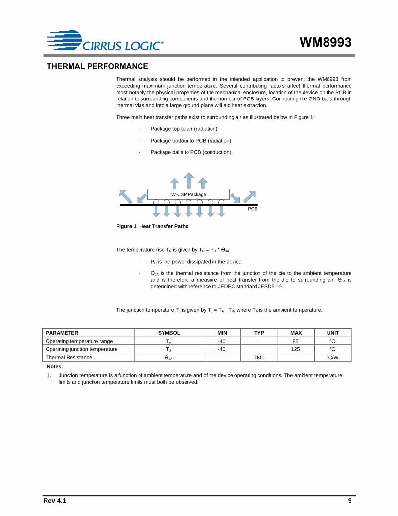
Three main heat transfer paths exist to surrounding air as illustrated below in Figure 1:
- Package top to air (radiation).
- Package bottom to PCB (radiation).
- Package balls to PCB (conduction).
W-CSP Package
PCB
Figure 1 Heat Transfer Paths
The temperature rise TR is given by TR = PD * ӨJA
- PD is the power dissipated in the device.
- ӨJA is the thermal resistance from the junction of the die to the ambient temperature
and is therefore a measure of heat transfer from the die to surrounding air. ӨJA is
determined with reference to JEDEC standard JESD51-9.
The junction temperature TJ is given by TJ = TA +TR, where TA is the ambient temperature.
PARAMETER SYMBOL MIN TYP MAX UNIT
Operating temperature range TA -40 85 °C
Operating junction temperature TJ -40 125 °C
Thermal Resistance ӨJA TBC °C/W
Notes:
1. Junction temperature is a function of ambient temperature and of the device operating conditions. The ambient temperature
limits and junction temperature limits must both be observed.
WM8993
Rev 4.1 10
ELECTRICAL CHARACTERISTICS
Test Conditions
DCVDD = 1.2V, AVDD2 = DBVDD = CPVDD = 1.8V, AVDD1 = 3.0V, SPKVDD = 5V, DGND=AGND=CPGND=SPKGND=0V,
TA = +25oC, 1kHz sinusoidal signal, fs = 48kHz, PGA gain = 0dB, 24-bit audio data unless otherwise stated.
PARAMETER TEST CONDITIONS MIN TYP MAX UNIT
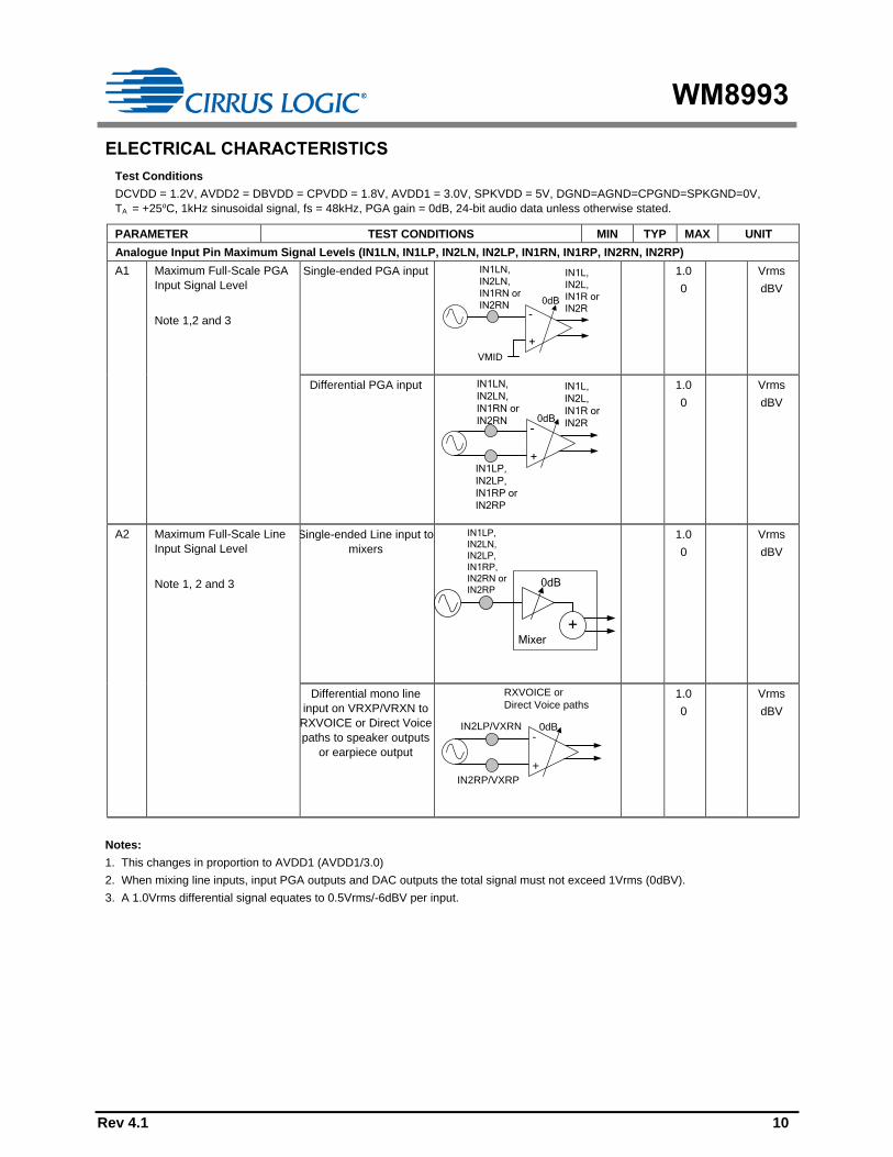
Analogue Input Pin Maximum Signal Levels (IN1LN, IN1LP, IN2LN, IN2LP, IN1RN, IN1RP, IN2RN, IN2RP)
A1 Maximum Full-Scale PGA
Input Signal Level
Note 1,2 and 3
Single-ended PGA input
-
+
0dB
IN1L,
IN2L,
IN1R or
IN2R
VMID
IN1LN,
IN2LN,
IN1RN or
IN2RN
1.0
0
Vrms
dBV
Differential PGA input
-
+
0dB
IN1L,
IN2L,
IN1R or
IN2R
IN1LN,
IN2LN,
IN1RN or
IN2RN
IN1LP,
IN2LP,
IN1RP or
IN2RP
1.0
0
Vrms
dBV
A2 Maximum Full-Scale Line
Input Signal Level
Note 1, 2 and 3
Single-ended Line input to
mixers
Mixer
0dB
IN1LP,
IN2LN,
IN2LP,
IN1RP,
IN2RN or
IN2RP
+
1.0
0
Vrms
dBV
Differential mono line
input on VRXP/VRXN to
RXVOICE or Direct Voice
paths to speaker outputs
or earpiece output
-
+
0dB
RXVOICE or
Direct Voice paths
IN2LP/VXRN
IN2RP/VXRP
1.0
0
Vrms
dBV
Notes:
1. This changes in proportion to AVDD1 (AVDD1/3.0)
2. When mixing line inputs, input PGA outputs and DAC outputs the total signal must not exceed 1Vrms (0dBV).
3. A 1.0Vrms differential signal equates to 0.5Vrms/-6dBV per input.

WM8993
Rev 4.1 11
Test Conditions
DCVDD = 1.2V, AVDD2 = DBVDD = CPVDD = 1.8V, AVDD1 = 3.0V, SPKVDD = 5V, DGND=AGND=CPGND=SPKGND=0V,
TA = +25oC, 1kHz sinusoidal signal, fs = 48kHz, PGA gain = 0dB, 24-bit audio data unless otherwise stated.
PARAMETER TEST CONDITIONS MIN TYP MAX UNIT
Analogue Input Pin Impedances (IN1LN, IN1LP, IN2LN, IN2LP, IN1RN, IN1RP, IN2RN, IN2RP)
B1 PGA Input Resistance
Differential Mode
Note 4
See “Applications
Information” for details of
Input resistance at all
PGA Gain settings.
PGA Gain = -16.5dB
RIN
-
+IN1L, IN2L,
IN1R or IN2R
RIN
IN1LN,
IN2LN,
IN1RN or
IN2RN
IN1LP,
IN2LP,
IN1RP or
IN2RP
52.5 k
PGA Gain = 0dB 25.1 k
PGA Gain = +30dB 1.3 k
B2 PGA Input Resistance
Single-Ended Mode
Note 4
See “Applications
Information” for details of
Input resistance at all
PGA Gain settings.
PGA Gain = -16.5dB
-
+IN1L, IN2L,
IN1R or IN2R
RIN
IN1LN,
IN2LN,
IN1RN or
IN2RN
VMID
58.0 k
PGA Gain = 0dB 36.2 k
PGA Gain = +30dB 2.5 k
B3 Line Input Resistance
Note 4
IN1LP or IN1RP to INMIXL
or INMIXR (-12dB)
MIXINL or MIXINR
RIN
RIN
IN1LP or
IN1RP
IN2LP or
IN2RP
+
56.0 k
IN1LP or IN1RP to INMIXL
or INMIXR (0dB)
17.4 k
IN1LP or IN1RP to INMIXL
or INMIXR (+6dB)
9.8 k
IN1LP to SPKMIXL or
IN1RP to SPKMIXR
(SPKATTN = -12dB) IN1LP or
IN1RP
SPKMIXL or
SPKMIXR
RIN
+
88.5 k
IN1LP to SPKMIXL or
IN1RP to SPKMIXR
(SPKATTN = 0dB)
26.7 k
IN2LN, IN2RN, IN2LP or
IN2RP to MIXOUTL or
MIXOUTR
(-21dB)
IN2LN,
IN2RN,
IN2LP or
IN2RP MIXOUTL or
MIXOUTR
RIN
+
150.9 k
IN2LN, IN2RN, IN2LP or
IN2RP to MIXOUTL or
MIXOUTR
(0dB)
18.2 k
VRXP-VRXN via RXVOICE
to MIXINL or MIXINR
(Gain = -12dB)
RXVOICERIN
RIN
VRXN
VRXP
MIXINL
or
MIXINR
47.7 k
VRXP-VRXN via RXVOICE
to MIXINL or MIXINR
(Gain = 0dB)
12.0 k
VRXP-VRXN via RXVOICE
to MIXINL or MIXINR
(Gain = +6dB)
6.0 k

WM8993
Rev 4.1 12
Test Conditions
DCVDD = 1.2V, AVDD2 = DBVDD = CPVDD = 1.8V, AVDD1 = 3.0V, SPKVDD = 5V, DGND=AGND=CPGND=SPKGND=0V,
TA = +25oC, 1kHz sinusoidal signal, fs = 48kHz, PGA gain = 0dB, 24-bit audio data unless otherwise stated.
PARAMETER TEST CONDITIONS MIN TYP MAX UNIT
Direct Voice to Earpiece
Driver (Gain = -6dB) RIN
RIN
VRXN
VRXP
HPOUT2P
HPOUT2N
Direct
Voice Path
33.3 k
Direct Voice to Earpiece
Driver (Gain = 0dB)
16.7 k
Direct Voice to Speaker
Driver (Gain = 0dB)
RIN
RIN
VRXN
VRXP
SPKOUTLP or
SPKOUTRP
SPKOUTLN or
SPKOUTRN
Direct
Voice Path
170.0 k
Direct Voice to Speaker
Driver (Gain = +6dB)
85.2 k
Direct Voice to Speaker
Driver (Gain = +9dB)
60.3 k
Direct Voice to Speaker
Driver (Gain = +12dB)
42.7 k
Note:
4. Input resistance will be seen in parallel with the resistance of other enabled input paths from the same pins
Test Conditions
DCVDD = 1.2V, AVDD2 = DBVDD = CPVDD = 1.8V, AVDD1 = 3.0V, SPKVDD = 5V, DGND=AGND=CPGND=SPKGND=0V,
TA = +25oC, 1kHz sinusoidal signal, fs = 48kHz, PGA gain = 0dB, 24-bit audio data unless otherwise stated.
PARAMETER TEST CONDITIONS MIN TYP MAX UNIT
Input Programmable Gain Amplifiers (PGAs) IN1L, IN2L, IN1R and IN2R
C1 Minimum Programmable Gain -16.5 dB
C2 Maximum Programmable Gain 30 dB
C3 Programmable Gain Step Size Guaranteed monotonic 1.5 dB
C4 Mute Attenuation Inputs disconnected 90 dB
C5 Common Mode Rejection Ratio
(217Hz input)
Single PGA in differential mode, gain = +30dB 70 dB
Single PGA in differential mode, gain = 0dB 60 dB
Single PGA in differential mode, gain = -16.5dB 55 dB
Input Mixers MIXINL and MIXINR
C6 Minimum Programmable Gain PGA Outputs to MIXINL and MIXINR 0 dB
C7 Maximum Programmable Gain PGA Outputs to MIXINL and MIXINR +30 dB
C8 Programmable Gain Step Size PGA Outputs to MIXINL and MIXINR 30 dB
C9 Minimum Programmable Gain Line Inputs and Record path to MIXINL and MIXINR -12 dB
C10 Maximum Programmable Gain Line Inputs and Record path to MIXINL and MIXINR +6 dB
C11 Programmable Gain Step Size Line Inputs and Record path to MIXINL and MIXINR 3 dB
C12 Minimum Programmable Gain RXVOICE to MIXINL and MIXINR -12 dB
C13 Maximum Programmable Gain RXVOICE to MIXINL and MIXINR +6 dB
C14 Programmable Gain Step Size RXVOICE to MIXINL and MIXINR 3 dB
C16 Common Mode Rejection Ratio
(217Hz input)
RXVOICE to MIXINL or MIXINR, gain = +6dB 60 dB
RXVOICE to MIXINL or MIXINR, gain = 0dB 65 dB
RXVOICE to MIXINL or MIXINR, gain = -12dB 65 dB

WM8993
Rev 4.1 13
Test Conditions
DCVDD = 1.2V, AVDD2 = DBVDD = CPVDD = 1.8V, AVDD1 = 3.0V, SPKVDD = 5V, DGND=AGND=CPGND=SPKGND=0V,
TA = +25oC, 1kHz sinusoidal signal, fs = 48kHz, PGA gain = 0dB, 24-bit audio data unless otherwise stated.
PARAMETER TEST CONDITIONS MIN TYP MAX UNIT
Output Mixers MIXOUTL and MIXOUTR
C17 Minimum Programmable Gain -21 dB
C18 Maximum Programmable Gain 0 dB
C19 Programmable Gain Step Size 3 dB
C20 Mute attenuation -67 dB
Speaker Mixers SPKMIXL and SPKMIXR
C21 Minimum Programmable Gain -15 dB
C22 Maximum Programmable Gain 0 dB
C23 Programmable Gain Step Size 3 dB
C24 Mute attenuation -67 dB
Output Programmable Gain Amplifiers (PGAs) HPOUT1LVOL, HPOUT1RVOL, MIXOUTLVOL, MIXOUTRVOL, SPKLVOL
and SPKRVOL
C25 Minimum Programmable Gain -57 dB
C26 Maximum Programmable Gain +6 dB
C27 Programmable Gain Step Size Guaranteed monotonic 1 dB
C28 Mute attenuation -69 dB
Line Output Driver Programmable Gain LINEOUT1NMIX, LINEOUT1PMIX, LINEOUT2NMIX and LINEOUT2PMIX
C29 Minimum Programmable Gain -6 dB
C30 Maximum Programmable Gain 0 dB
C31 Programmable Gain Step Size 6 dB
Earpiece Driver Programmable Gain HPOUT2MIX
C33 Minimum Programmable Gain -6 dB
C34 Maximum Programmable Gain 0 dB
C35 Programmable Gain Step Size 6 dB
C37 Common Mode Rejection Ratio
(217Hz input)
Direct Voice path to HPOUT2, gain = 0dB 50 dB
Speaker Output Driver Programmable Gain SPKOUTLBOOST and SPKOUTRBOOST
C38 Minimum Programmable Gain 0 dB
C39 Maximum Programmable Gain +12 dB
C40 Programmable Gain Step Size 1.5 dB
C42 Mute attenuation Class AB mode -78 dB
C43 Common Mode Rejection Ratio
(217Hz input)
Direct Voice path to SPKOUTL or SPKOUTR,
gain = 0dB
50 dB
Direct Voice path to SPKOUTL or SPKOUTR,
gain = +12dB
50 dB

WM8993
Rev 4.1 14
Test Conditions
DCVDD = 1.2V, AVDD2 = DBVDD = CPVDD = 1.8V, AVDD1 = 3.0V, SPKVDD = 5V, DGND=AGND=CPGND=SPKGND=0V,
TA = +25oC, 1kHz sinusoidal signal, fs = 48kHz, PGA gain = 0dB, 24-bit audio data unless otherwise stated.
PARAMETER TEST CONDITIONS MIN TYP MAX UNIT
ADC Input Path Performance
D1 Line Inputs to ADC via MIXINL and MIXINR
SNR (A-weighted)
MIXINL or MIXINR
IN1LP or
IN1RP+
ADC L
or ADCR
94 dB
THD (-1dBFS input) -83 dB
THD+N (-1dBFS input) -81 dB
Crosstalk (L/R) -100 dB
PSRR (all other supplies
217Hz) 100mVpk-pk
-78 dB
D2 Record Path (DACs to ADCs via MIXINL and MIXINR)
SNR (A-weighted)
MIXINL or MIXINR
+ ADC L
or ADCR
DAC L
or DACR
83 94 dB
THD (-1dBFS input) -74 -64 dB
THD+N (-1dBFS input) -72 -62 dB
Crosstalk (L/R) -95 dB
D3 Input PGAs to ADC via MIXINL or MIXINR
SNR (A-weighted)
-
+
0dB MIXINL or
MIXINR
IN1L, IN2L,
IN1R or IN2R
(Single-ended or
differential mode)
IN1LN, IN2LN,
IN1RN or IN2RN
IN1LP, IN2LP,
IN1RP or IN2RP
+ ADCL or
ADCR
86 95 dB
THD (-1dBFS input) -82 -72 dB
THD+N (-1dBFS input) -80 -70 dB
Crosstalk (L/R) -100 dB
PSRR (AVDD1 217Hz) 100mVpk-pk -100 dB
D4 VRXP-VRXN to one ADC via RXVOICE
SNR (A-weighted)
RXVOICEVRXN
VRXP
MIXINL or
MIXINR
+ ADCL or
ADCR
95 dB
THD (-1dBFS input) -83 dB
THD+N (-1dBFS input) -81 dB

WM8993
Rev 4.1 15
Test Conditions
DCVDD = 1.2V, AVDD2 = DBVDD = CPVDD = 1.8V, AVDD1 = 3.0V, SPKVDD = 5V, DGND=AGND=CPGND=SPKGND=0V,
TA = +25oC, 1kHz sinusoidal signal, fs = 48kHz, PGA gain = 0dB, 24-bit audio data unless otherwise stated.
PARAMETER TEST CONDITIONS MIN TYP MAX UNIT
DAC Output Path Performance
E1 DAC to Single-Ended Line Output (10k / 50pF)
SNR (A-weighted)
MIXOUTL or
MIXOUTR
+DACL or
DACR
0dB
MIXOUTLVOL
or
MIXOUTRVOL
LINEOUT1N,
LINEOUT1P,
LINEOUT2N,
LINEOUT2P
0dB
LINEOUT1NMIX,
LINEOUT1PMIX,
LINEOUT2NMIX,
LINEOUT2PMIX
+
84 94 dB
THD 0dBFS input -71 -61 dB
THD+N 0dBFS input -70 -60 dB
Crosstalk (L/R) -75 dB
PSRR (all other supplies
217Hz) 100mVpk-pk -36 dB
E2 DAC to Differential Line Output (10k / 50pF)
SNR (A-weighted)
MIXOUTL
+DACL or
DACR0dB
LINEOUT1PMIX
or
LINEOUT2PMIX
0dB
0dB
MIXOUTLVOL
LINEOUT1NMIX
or
LINEOUT2NMIXLINEOUT1N
or
LINEOUT2N
LINEOUT1P
or
LINEOUT2P
+
+
87 97 dB
THD 0dBFS input -76 dB
THD+N 0dBFS input -75 dB
Crosstalk (L/R) -90 dB
PSRR (all other supplies
217Hz) 100mVpk-pk -51 dB
E3 Minimum Line Output
Resistance
LINEOUT1N,
LINEOUT1P,
LINEOUT2N,
LINEOUT2P
2 k
E4 Line Output Capacitance LINEOUT1N,
LINEOUT1P,
LINEOUT2N,
LINEOUT2P
Direct connection 100 pF
Connection via 1k series resistor 2000 pF
E5 DAC to Headphone on HPOUT1L or HPOUT1R (RL=32)
SNR (A-weighted) OSR = 128fs
DACL or
DACR
HPOUT1LVOL
or
HPOUT1RVOL
Rload=
32ohm
HPOUT1L
or
HPOUT1R
100 dB
OSR = 64fs 97 dB
THD (PO=20mW) -79 dB
THD+N (PO=20mW) -77 dB
THD (PO=5mW) -83 dB
THD+N (PO=5mW) -81 dB
Crosstalk (L/R) -95 dB
PSRR (all other supplies
217Hz)
100mVpk-pk -51 dB
E6 DAC to Headphone on HPOUT1L or HPOUT1R (RL=16)
SNR (A-weighted) OSR = 128fs
DACL or
DACR
HPOUT1LVOL
or
HPOUT1RVOL
Rload=
16ohm
HPOUT1L
or
HPOUT1R
90 100 dB
OSR = 64fs 97 dB
THD (PO=20mW) -85 dB
THD+N (PO=20mW) -83 dB
THD (PO=5mW) -83 -73 dB
THD+N (PO=5mW) -81 -71 dB
Crosstalk (L/R) -95 dB
PSRR (all other supplies
217Hz)
100mVpk-pk -51 dB

WM8993
Rev 4.1 16
Test Conditions
DCVDD = 1.2V, AVDD2 = DBVDD = CPVDD = 1.8V, AVDD1 = 3.0V, SPKVDD = 5V, DGND=AGND=CPGND=SPKGND=0V,
TA = +25oC, 1kHz sinusoidal signal, fs = 48kHz, PGA gain = 0dB, 24-bit audio data unless otherwise stated.
PARAMETER TEST CONDITIONS MIN TYP MAX UNIT
E7 Minimum Headphone
Resistance
HPOUT1L or
HPOUT1R
Normal operation 15
Device survival with load applied indefinitely 1
E8 Headphone Capacitance HPOUT1L or
HPOUT1R
2 nF
E9 DAC to Earpiece Driver (RL=16 BTL)
SNR (A-weighted)
MIXOUTL
or
MIXOUTR
HPOUT2MIX
RLOAD
=16ohm
MIXOUTLVOL
or
MIXOUTRVOL
+DACL or
DACR +
HPOUT2N
0dB
HPOUT2P
97 dB
THD (PO=50mW) -69 dB
THD+N (PO=50mW) -67 dB
PSRR (all other supplies
217Hz)
100mVpk-pk -51 dB
DC Offset at Load 5 mV
E10 Earpiece Resistance 15
E11 Earpiece Capacitance Direct connection 200 pF
E12 DAC to Speaker Outputs (RL=8 + 10H BTL, Stereo Mode)
SNR (A-weighted)
Class D mode
SPK Boost=+12dB
SPKMIXL or
SPKMIXR
+DACL or
DACR +
SPKLVOL or
SPKRVOL 0dB
SPKOUTLBOOST
or
SPKOUTRBOOST
RLOAD=
8ohm
SPKOUTLP or
SPKOUTRP
SPKOUTLN or
SPKOUTRN
84 94 dB
THD (PO=0.5W) -63 -53 dB
THD+N (PO=0.5W) -62 -52 dB
THD (PO=1.0W) -67 dB
THD+N (PO=1.0W) -66 dB
PSRR (all supplies
217Hz)
-43 dB
Crosstalk (L/R) -80 dB
SNR (A-weighted)
Class AB mode
SPK Boost=+12dB
97 dB
THD (PO=0.5W) -68 dB
THD+N (PO=0.5W) -65 dB
THD (PO=1.0W) -70 dB
THD+N (PO=1.0W) -68 dB
PSRR (all supplies
217Hz)
-43 dB
Crosstalk (L/R) -80 dB
DC Offset at Load Class AB mode
SPK Boost=0dB
10 mV
WM8993
Rev 4.1 17
Test Conditions
DCVDD = 1.2V, AVDD2 = DBVDD = CPVDD = 1.8V, AVDD1 = 3.0V, SPKVDD = 5V, DGND=AGND=CPGND=SPKGND=0V,
TA = +25oC, 1kHz sinusoidal signal, fs = 48kHz, PGA gain = 0dB, 24-bit audio data unless otherwise stated.
PARAMETER TEST CONDITIONS MIN TYP MAX UNIT
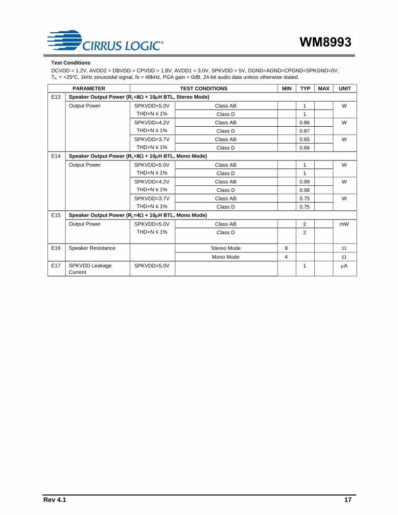
E13 Speaker Output Power (RL=8 + 10H BTL, Stereo Mode)
Output Power
SPKVDD=5.0V
THD+N ≤ 1%
Class AB 1 W
Class D 1
SPKVDD=4.2V
THD+N ≤ 1%
Class AB 0.86 W
Class D 0.87
SPKVDD=3.7V
THD+N ≤ 1%
Class AB 0.65 W
Class D 0.66
E14 Speaker Output Power (RL=8 + 10H BTL, Mono Mode)
Output Power
SPKVDD=5.0V
THD+N ≤ 1%
Class AB 1 W
Class D 1
SPKVDD=4.2V
THD+N ≤ 1%
Class AB 0.99 W
Class D 0.98
SPKVDD=3.7V
THD+N ≤ 1%
Class AB 0.75 W
Class D 0.75
E15 Speaker Output Power (RL=4 + 10H BTL, Mono Mode)
Output Power
SPKVDD=5.0V
THD+N ≤ 1%
Class AB 2 mW
Class D 2
E16 Speaker Resistance Stereo Mode 8
Mono Mode 4
E17 SPKVDD Leakage
Current
SPKVDD=5.0V 1 A

WM8993
Rev 4.1 18
Test Conditions
DCVDD = 1.2V, AVDD2 = DBVDD = CPVDD = 1.8V, AVDD1 = 3.0V, SPKVDD = 5V, DGND=AGND=CPGND=SPKGND=0V,
TA = +25oC, 1kHz sinusoidal signal, fs = 48kHz, PGA gain = 0dB, 24-bit audio data unless otherwise stated.
PARAMETER TEST CONDITIONS MIN TYP MAX UNIT
Bypass Path Performance
F1 Input PGA to Differential Line Out (10k / 50pF)
SNR (A-weighted)
0dB
LINEOUT1PMIX
or
LINEOUT2PMIX
0dB
0dB
IN1L or IN1R
(Single-ended
or Differential)
LINEOUT1NMIX
or
LINEOUT2NMIXLINEOUT1N
or
LINEOUT2N
LINEOUT1P
or
LINEOUT2P
+
+
IN1LN or
IN1RN
IN1LP or
IN1RP
-
+
92 102 dB
THD (0dB output) -94 -84 dB
THD+N (0dB output) -92 -82 dB
PSRR (all other supplies
217Hz)
100mVpk-pk -45 dB
F2 VRXP or VRXN to Headphone via MIXOUTL or MIXOUTR (RL=16)
SNR (A-weighted)
MIXOUTL
or
MIXOUTR
VRXN or
VRXP HPOUT1LVOL
or
HPOUT1RVOL
+
0dB
Rload=
16ohm
HPOUT1L or
HPOUT1R
101 dB
THD (PO=20mW) -85 dB
THD+N (PO=20mW) -83 dB
THD (PO=5mW) -83 dB
THD+N (PO=5mW) -81 dB
PSRR (all other supplies
217Hz)
100mVpk-pk -49 dB
F3 Input PGA to Headphone via MIXOUTL or MIXOUTR (RL=16)
SNR (A-weighted)
-
+
0dB
IN1L or IN1R
(Single-ended
or Differential)
0dB
MIXOUTL
or
MIXOUTR
+
IN1LN or
IN1RN
IN1LP or
IN1RPHPOUT1LVOL
or
HPOUT1RVOL
HPOUT1L or
HPOUT1R
Rload=
16ohm
100 dB
THD (PO=20mW) -85 dB
THD+N (PO=20mW) -83 dB
THD (PO=5mW) -83 dB
THD+N (PO=5mW) -81 dB
PSRR (all other supplies
217Hz)
100mVpk-pk -49 dB
Crosstalk (L/R) -95 dB
F4 Line Input to Headphone via MIXOUTL and MIXOUTR (RL=16)
SNR (A-weighted)
0dB
MIXOUTL or
MIXOUTR
+IN2LN or
IN2RN HPOUT1LVOL or
HPOUT1RVOL
HPOUT1L or
HPOUT1R
Rload=
16ohm
92 100 dB
THD (PO=20mW) -85 -75 dB
THD+N (PO=20mW) -83 -73 dB
THD (PO=5mW) -83 dB
THD+N (PO=5mW) -81 dB
PSRR (all other supplies
217Hz)
100mVpk-pk -49 dB
Crosstalk (L/R) -95 dB
F5 VRXP-VRXN Direct Voice Path to Earpiece Driver (RL=16 BTL)
SNR (A-weighted)
HPOUT2P
HPOUT2N
VRXN
VRXP
Direct
Voice
Path
0dB
Rload=
16ohm
90 104 dB
THD (PO=50mW) -69 -60 dB
THD+N (PO=50mW) -67 -58 dB
PSRR (all other supplies
217Hz)
100mVpk-pk -91 dB
DC Offset at Load 5 mV

WM8993
Rev 4.1 19
Test Conditions
DCVDD = 1.2V, AVDD2 = DBVDD = CPVDD = 1.8V, AVDD1 = 3.0V, SPKVDD = 5V, DGND=AGND=CPGND=SPKGND=0V,
TA = +25oC, 1kHz sinusoidal signal, fs = 48kHz, PGA gain = 0dB, 24-bit audio data unless otherwise stated.
PARAMETER TEST CONDITIONS MIN TYP MAX UNIT
F6 VRXP-VRXN Direct Voice Path to Speaker Outputs (RL=8 BTL)
SNR (A-weighted)
Class D Mode
SPK Boost=+12dB
VRXN
VRXP
Direct
Voice
Path
0dB
Rload
=8ohm
SPKOUTLP or
SPKOUTRP
SPKOUTLN or
SPKOUTRN
97 dB
THD (PO=0.5W) -63 dB
THD+N (PO=0.5W) -62 dB
THD (PO=1.0W) -67 dB
THD+N (PO=1.0W) -65 dB
PSRR (all supplies
217Hz)
-63 dB
SNR (A-weighted)
Class AB Mode
SPK Boost=+12dB
104 dB
THD (PO=0.5W) -68 dB
THD+N (PO=0.5W) -65 dB
THD (PO=1.0W) -70 dB
THD+N (PO=1.0W) -68 dB
PSRR (all supplies
217Hz)
-67 dB
DC Offset at Load Class AB Mode
SPK Boost=0dB
10 mV
F7 Line Input to Speaker Outputs via SPKMIXL or SPKMIXR (RL=8 BTL)
SNR (A-weighted)
Class D Mode
SPK Boost =+12dB
RLOAD =
8ohmSPKMIXL or
SPKMIXR
+
0dBIN1LP or
IN1RP
SPKLVOL or
SPKRVOL
+
SPKOUTLBOOST
or
SPKOUTRBOOST SPKOUTLN or
SPKOUTRN
SPKOUTLP or
SPKOUTRP
93 dB
THD (PO=0.5W) -63 dB
THD+N (PO=0.5W) -62 dB
THD (PO=1.0W) -67 dB
THD+N (PO=1.0W) -65 dB
PSRR (all other supplies
217Hz)
-47 dB
SNR (A-weighted)
Class AB Mode
SPK Boost=+12dB
86 96 dB
THD (PO=0.5W) -68 -59 dB
THD+N (PO=0.5W) -65 -57 dB
THD (PO=1.0W) -70 dB
THD+N (PO=1.0W) -68 dB
PSRR (all other supplies
217Hz)
-47 dB
DC Offset at Load Class AB Mode
SPK Boost=0dB
10 mV
WM8993
Rev 4.1 20
Test Conditions
DCVDD = 1.2V, AVDD2 = DBVDD = CPVDD = 1.8V, AVDD1 = 3.0V, SPKVDD = 5V, DGND=AGND=CPGND=SPKGND=0V,
TA = +25oC, 1kHz sinusoidal signal, fs = 48kHz, PGA gain = 0dB, 24-bit audio data unless otherwise stated.
PARAMETER TEST CONDITIONS MIN TYP MAX UNIT
Multi-Path Channel Separation
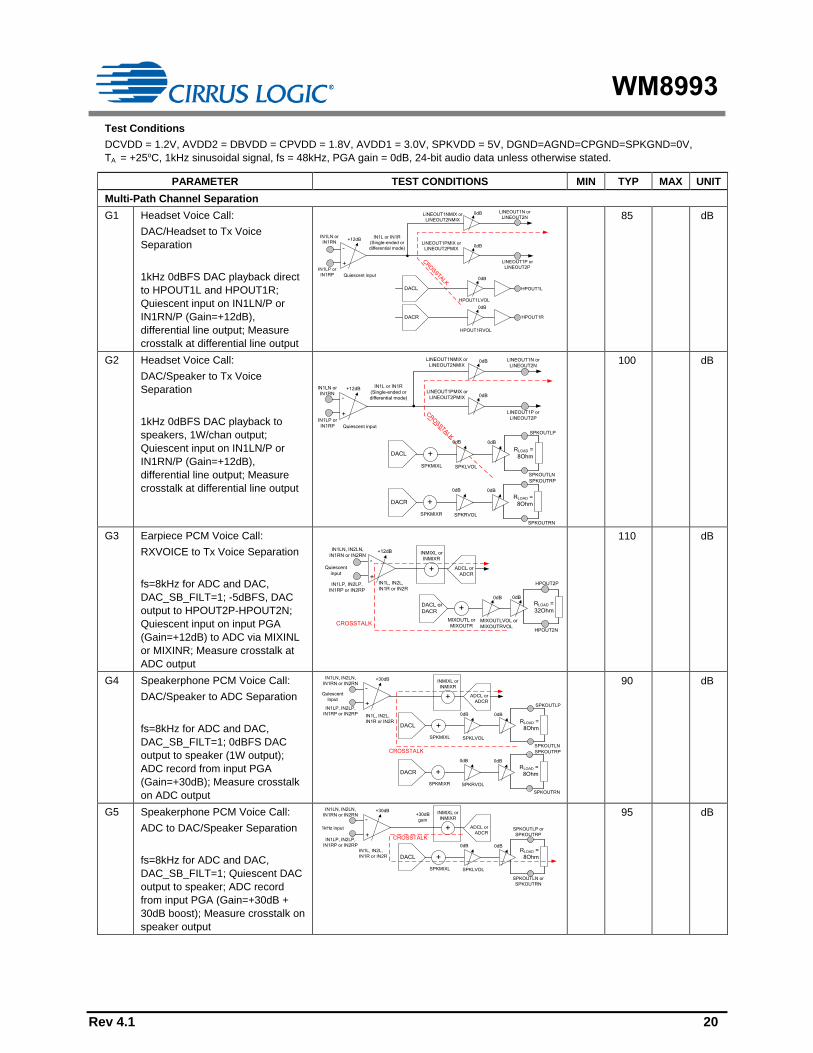
G1 Headset Voice Call:
DAC/Headset to Tx Voice
Separation
1kHz 0dBFS DAC playback direct
to HPOUT1L and HPOUT1R;
Quiescent input on IN1LN/P or
IN1RN/P (Gain=+12dB),
differential line output; Measure
crosstalk at differential line output
-
+
+12dBIN1L or IN1R
(Single-ended or
differential mode)0dB
0dB
Quiescent input
DACR
0dB
DACL
0dB
HPOUT1L
HPOUT1R
IN1LP or
IN1RP
IN1LN or
IN1RN
LINEOUT1N or
LINEOUT2N
LINEOUT1P or
LINEOUT2P
LINEOUT1NMIX or
LINEOUT2NMIX
CRO
SSTA
LK
HPOUT1LVOL
HPOUT1RVOL
LINEOUT1PMIX or
LINEOUT2PMIX
85 dB
G2 Headset Voice Call:
DAC/Speaker to Tx Voice
Separation
1kHz 0dBFS DAC playback to
speakers, 1W/chan output;
Quiescent input on IN1LN/P or
IN1RN/P (Gain=+12dB),
differential line output; Measure
crosstalk at differential line output
-
+
+12dBIN1L or IN1R
(Single-ended or
differential mode)0dB
0dB
+
SPKMIXL
CRO
SSTA
LK
Quiescent input
DACLRLOAD =
8Ohm
0dB
LINEOUT1N or
LINEOUT2N
LINEOUT1P or
LINEOUT2P
SPKOUTLP
SPKOUTLN
IN1LP or
IN1RP
IN1LN or
IN1RN
0dB
SPKLVOL
+
SPKMIXR
RLOAD =
8Ohm
0dB
SPKOUTRP
SPKOUTRN
0dB
SPKRVOL
DACR
LINEOUT1NMIX or
LINEOUT2NMIX
LINEOUT1PMIX or
LINEOUT2PMIX
100 dB
G3 Earpiece PCM Voice Call:
RXVOICE to Tx Voice Separation
fs=8kHz for ADC and DAC,
DAC_SB_FILT=1; -5dBFS, DAC
output to HPOUT2P-HPOUT2N;
Quiescent input on input PGA
(Gain=+12dB) to ADC via MIXINL
or MIXINR; Measure crosstalk at
ADC output
RLOAD =
32Ohm
MIXOUTLVOL or
MIXOUTRVOL
0dB 0dB
DACL or
DACR +
MIXOUTL or
MIXOUTR
+-
+
+12dB INMIXL or
INMIXR
IN1L, IN2L,
IN1R or IN2R
ADCL or
ADCR
CROSSTALK
Quiescent
input
IN1LN, IN2LN,
IN1RN or IN2RN
IN1LP, IN2LP,
IN1RP or IN2RP
HPOUT2P
HPOUT2N
110 dB
G4 Speakerphone PCM Voice Call:
DAC/Speaker to ADC Separation
fs=8kHz for ADC and DAC,
DAC_SB_FILT=1; 0dBFS DAC
output to speaker (1W output);
ADC record from input PGA
(Gain=+30dB); Measure crosstalk
on ADC output
+
INMIXL or
INMIXR
ADCL or
ADCR
CROSSTALK
-
+
+30dB
IN1L, IN2L,
IN1R or IN2R
Quiescent
input
IN1LN, IN2LN,
IN1RN or IN2RN
IN1LP, IN2LP,
IN1RP or IN2RP
+
SPKMIXL
DACLRLOAD =
8Ohm
0dB
SPKOUTLP
SPKOUTLN
0dB
SPKLVOL
+
SPKMIXR
RLOAD =
8Ohm
0dB
SPKOUTRP
SPKOUTRN
0dB
SPKRVOL
DACR
90 dB
G5 Speakerphone PCM Voice Call:
ADC to DAC/Speaker Separation
fs=8kHz for ADC and DAC,
DAC_SB_FILT=1; Quiescent DAC
output to speaker; ADC record
from input PGA (Gain=+30dB +
30dB boost); Measure crosstalk on
speaker output
+
INMIXL or
INMIXR
ADCL or
ADCR
-
+
+30dB
IN1L, IN2L,
IN1R or IN2R
1kHz input
IN1LN, IN2LN,
IN1RN or IN2RN
IN1LP, IN2LP,
IN1RP or IN2RP
+
SPKMIXL
DACL
RLOAD =
8Ohm
0dB
SPKOUTLP or
SPKOUTRP
SPKOUTLN or
SPKOUTRN
0dB
SPKLVOL
+30dB
gain
CROSSTALK
95 dB

WM8993
Rev 4.1 21
Test Conditions
DCVDD = 1.2V, AVDD2 = DBVDD = CPVDD = 1.8V, AVDD1 = 3.0V, SPKVDD = 5V, DGND=AGND=CPGND=SPKGND=0V,
TA = +25oC, 1kHz sinusoidal signal, fs = 48kHz, PGA gain = 0dB, 24-bit audio data unless otherwise stated.
PARAMETER TEST CONDITIONS MIN TYP MAX UNIT
G6 Earpiece Speaker Voice Call:
Tx Voice and RXVOICE
Separation
1kHz Full scale differential input
on VRXP-VRXN, output to
HPOUT2P-HPOUT2N; Quiescent
input on IN1LN/P or IN1RN/P
(Gain=+12dB), differential line
output; Measure crosstalk at
differential line output
-
+
+12dBIN1L or IN1R
(Single-ended or
differential mode) 0dB
0dB
0dB
32Ω
LOADFull scale input
CR
OS
STA
LK
Quiescent input
IN1LN or
IN1RN
IN1LP or
IN1RP
LINEOUT1N or
LINEOUT2N
LINEOUT1P or
LINEOUT2P
HPOUT2L
HPOUT2R
VRXN
VRXP
Direct Voice
Path
LINEOUT1NMIX or
LINEOUT2NMIX
LINEOUT1PMIX or
LINEOUT2PMIX
100 dB
G7 Headset Voice Call:
Tx Voice and RXVOICE
Separation
1kHz full scale differential input on
VRXP-VRXN via RXVOICE to
MIXOUTL and MIXOUTR, output
to HPOUT1L and HPOUT1R;
Quiescent input on IN1LN/P or
IN1RN/P (Gain=+12dB),
differential line output; Measure
crosstalk at differential line output
-
+
+12dBIN1L or IN1R
(Single-ended or
differential mode)0dB
0dB
+
0dB
+
0dB
MIXOUTL
MIXOUTR
Full scale
input
CR
OS
STA
LK
Quiescent input
RXVOICE
(MIXINL or
MIXINR)
-
+
IN1LN or
IN1RN
IN1LP or
IN1RP
VRXN
VRXP
HPOUT1L
HPOUT1R
LINEOUT1P or
LINEOUT2P
LINEOUT1N or
LINEOUT2N
LINEOUT1NMIX or
LINEOUT2NMIX
HPOUT1LVOL
HPOUT1RVOL
LINEOUT1PMIX or
LINEOUT2PMIX
90 dB
G8 Stereo Line Record and Playback:
DAC/Headset to ADC Separation
-5dBFS input to DACs, playback to
HPOUT1L and HPOUT1R; ADC
record from line input; Measure
crosstalk on ADC output
DACR
HPOUT1LVOL
0dB
DACL
HPOUT1RVOL
0dB
+
INMIXL or
INMIXR
ADCL or
ADCR
CROSSTALK
Quiescent
input
HPOUT1L
HPOUT1R
IN1LP or
IN1RP
95 dB
WM8993
Rev 4.1 22
Test Conditions
DCVDD = 1.2V, AVDD2 = DBVDD = CPVDD = 1.8V, AVDD1 = 3.0V, SPKVDD = 5V, DGND=AGND=CPGND=SPKGND=0V,
TA = +25oC, 1kHz sinusoidal signal, fs = 48kHz, PGA gain = 0dB, 24-bit audio data unless otherwise stated.
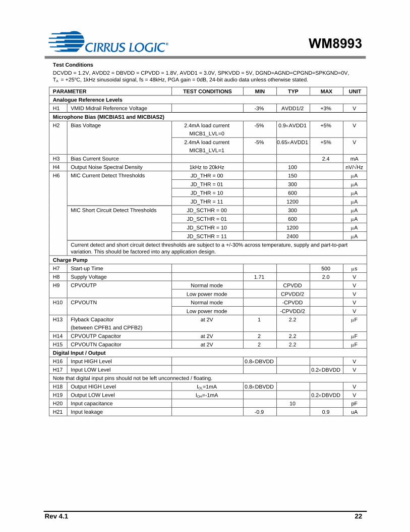
PARAMETER TEST CONDITIONS MIN TYP MAX UNIT
Analogue Reference Levels
H1 VMID Midrail Reference Voltage -3% AVDD1/2 +3% V
Microphone Bias (MICBIAS1 and MICBIAS2)
H2 Bias Voltage 2.4mA load current
MICB1_LVL=0
-5% 0.9AVDD1 +5% V
2.4mA load current
MICB1_LVL=1
-5% 0.65AVDD1 +5% V
H3 Bias Current Source 2.4 mA
H4 Output Noise Spectral Density 1kHz to 20kHz 100 nV/Hz
H6 MIC Current Detect Thresholds JD_THR = 00 150 A
JD_THR = 01 300 A
JD_THR = 10 600 A
JD_THR = 11 1200 A
MIC Short Circuit Detect Thresholds JD_SCTHR = 00 300 A
JD_SCTHR = 01 600 A
JD_SCTHR = 10 1200 A
JD_SCTHR = 11 2400 A
Current detect and short circuit detect thresholds are subject to a +/-30% across temperature, supply and part-to-part
variation. This should be factored into any application design.
Charge Pump
H7 Start-up Time 500 s
H8 Supply Voltage 1.71 2.0 V
H9 CPVOUTP Normal mode CPVDD V
Low power mode CPVDD/2 V
H10 CPVOUTN Normal mode -CPVDD V
Low power mode -CPVDD/2 V
H13 Flyback Capacitor
(between CPFB1 and CPFB2)
at 2V 1 2.2 F
H14 CPVOUTP Capacitor at 2V 2 2.2 F
H15 CPVOUTN Capacitor at 2V 2 2.2 F
Digital Input / Output
H16 Input HIGH Level 0.8DBVDD V
H17 Input LOW Level 0.2DBVDD V
Note that digital input pins should not be left unconnected / floating.
H18 Output HIGH Level IOL=1mA 0.8DBVDD V
H19 Output LOW Level IOH=-1mA 0.2DBVDD V
H20 Input capacitance 10 pF
H21 Input leakage -0.9 0.9 uA

WM8993
Rev 4.1 23
Test Conditions
DCVDD = 1.2V, AVDD2 = DBVDD = CPVDD = 1.8V, AVDD1 = 3.0V, SPKVDD = 5V, DGND=AGND=CPGND=SPKGND=0V,
TA = +25oC, 1kHz sinusoidal signal, fs = 48kHz, PGA gain = 0dB, 24-bit audio data unless otherwise stated.
PARAMETER TEST CONDITIONS MIN TYP MAX UNIT
FLL
H22 Input Frequency FLL_CLK_REF_DIV = 00 0.032 13.5 MHz
FLL_CLK_REF_DIV = 01 0.032 27 MHz
H23 Lock time FREF=32kHz,
FOUT=12.288MHz
2.5 ms
FREF=12MHz,
FOUT=12.288MHz
300 s
H24 Free-running mode start-up time VMID enabled 100 s
H25 Free-running mode frequency accuracy Reference supplied initially +/-10 %
No reference provided +/-30 %
GPIO
H26 Interrupt response time for accessory /
button detect
Input de-bounced 219 / fCLK_SYS 222 / fCLK_SYS s
Input not de-bounced 0 s
TERMINOLOGY
1. Signal-to-Noise Ratio (dB) – SNR is a measure of the difference in level between the maximum full scale output signal and the
output with no input signal applied.
2. Total Harmonic Distortion (dB) – THD is the level of the rms value of the sum of harmonic distortion products relative to the
amplitude of the measured output signal.
3. Total Harmonic Distortion plus Noise (dB) – THD+N is the level of the rms value of the sum of harmonic distortion products
plus noise in the specified bandwidth relative to the amplitude of the measured output signal.
4. Crosstalk (L/R) (dB) – left-to-right and right-to-left channel crosstalk is the measured signal level in the idle channel at the test
signal frequency relative to the signal level at the output of the active channel. The active channel is configured and supplied
with an appropriate input signal to drive a full scale output, with signal measured at the output of the associated idle channel.
5. Multi-Path Channel Separation (dB) – is the measured signal level in the idle path at the test signal frequency relative to the
signal level at the output of the active path. The active path is configured and supplied with an appropriate input signal to drive
a full scale output, with signal measured at the output of the specified idle path.
6. Mute Attenuation – This is a measure of the difference in level between the full scale output signal and the output with mute
applied.
7. All performance measurements carried out with 20kHz low pass filter, and where noted an A-weighted filter. Failure to use such
a filter will result in higher THD and lower SNR readings than are found in the Electrical Characteristics. The low pass filter
removes out of band noise; although it is not audible it may affect dynamic specification values.
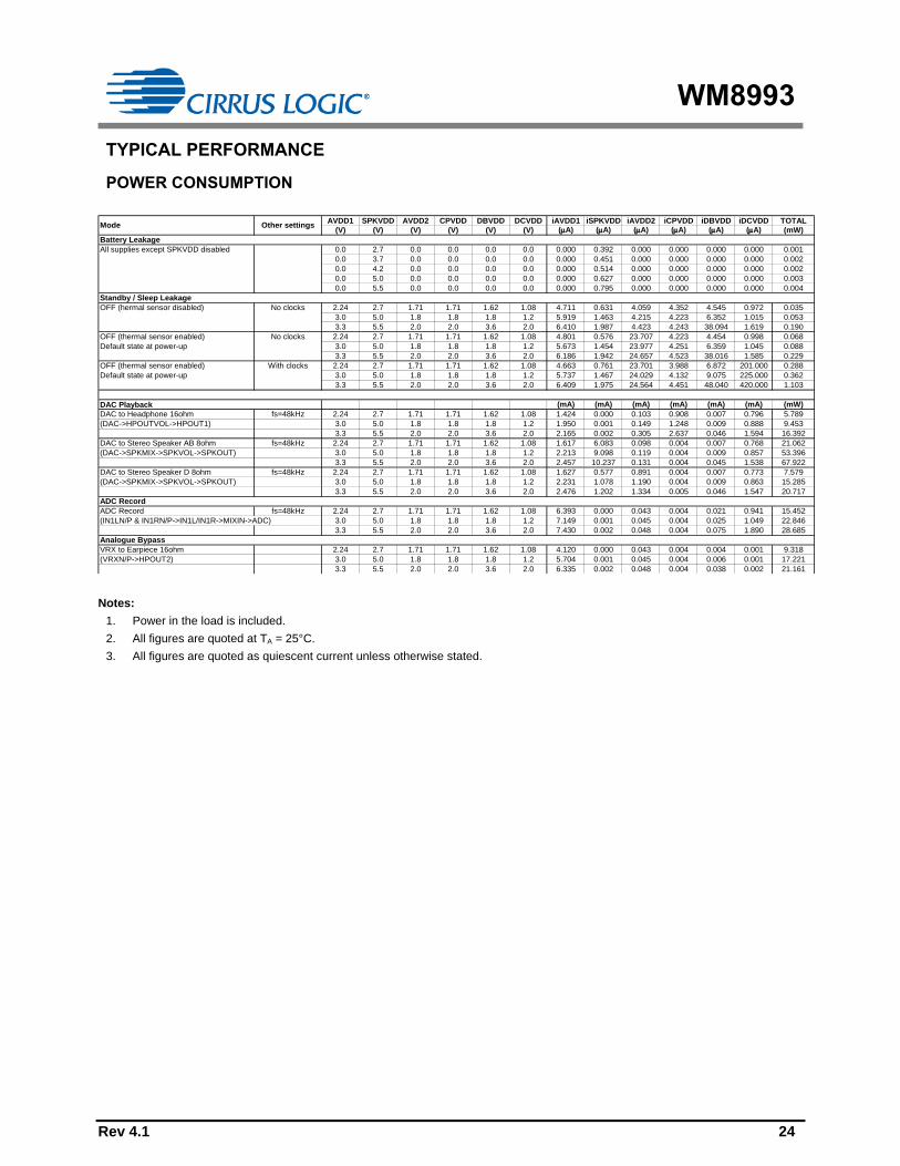
WM8993
Rev 4.1 24
TYPICAL PERFORMANCE
POWER CONSUMPTION
AVDD1 SPKVDD AVDD2 CPVDD DBVDD DCVDD iAVDD1 iSPKVDD iAVDD2 iCPVDD iDBVDD iDCVDD TOTAL
(V) (V) (V) (V) (V) (V) (A) (A) (A) (A) (A) (A) (mW)
All supplies except SPKVDD disabled 0.0 2.7 0.0 0.0 0.0 0.0 0.000 0.392 0.000 0.000 0.000 0.000 0.001
0.0 3.7 0.0 0.0 0.0 0.0 0.000 0.451 0.000 0.000 0.000 0.000 0.002
0.0 4.2 0.0 0.0 0.0 0.0 0.000 0.514 0.000 0.000 0.000 0.000 0.002
0.0 5.0 0.0 0.0 0.0 0.0 0.000 0.627 0.000 0.000 0.000 0.000 0.003
0.0 5.5 0.0 0.0 0.0 0.0 0.000 0.795 0.000 0.000 0.000 0.000 0.004
OFF (hermal sensor disabled) No clocks 2.24 2.7 1.71 1.71 1.62 1.08 4.711 0.631 4.059 4.352 4.545 0.972 0.035
3.0 5.0 1.8 1.8 1.8 1.2 5.919 1.463 4.215 4.223 6.352 1.015 0.053
3.3 5.5 2.0 2.0 3.6 2.0 6.410 1.987 4.423 4.243 38.094 1.619 0.190
OFF (thermal sensor enabled) No clocks 2.24 2.7 1.71 1.71 1.62 1.08 4.801 0.576 23.707 4.223 4.454 0.998 0.068
Default state at power-up 3.0 5.0 1.8 1.8 1.8 1.2 5.673 1.454 23.977 4.251 6.359 1.045 0.088
3.3 5.5 2.0 2.0 3.6 2.0 6.186 1.942 24.657 4.523 38.016 1.585 0.229
OFF (thermal sensor enabled) With clocks 2.24 2.7 1.71 1.71 1.62 1.08 4.663 0.761 23.701 3.988 6.872 201.000 0.288
Default state at power-up 3.0 5.0 1.8 1.8 1.8 1.2 5.737 1.467 24.029 4.132 9.075 225.000 0.362
3.3 5.5 2.0 2.0 3.6 2.0 6.409 1.975 24.564 4.451 48.040 420.000 1.103
DAC Playback (mA) (mA) (mA) (mA) (mA) (mA) (mW)
DAC to Headphone 16ohm fs=48kHz 2.24 2.7 1.71 1.71 1.62 1.08 1.424 0.000 0.103 0.908 0.007 0.796 5.789
(DAC->HPOUTVOL->HPOUT1) 3.0 5.0 1.8 1.8 1.8 1.2 1.950 0.001 0.149 1.248 0.009 0.888 9.453
3.3 5.5 2.0 2.0 3.6 2.0 2.165 0.002 0.305 2.637 0.046 1.594 16.392
DAC to Stereo Speaker AB 8ohm fs=48kHz 2.24 2.7 1.71 1.71 1.62 1.08 1.617 6.083 0.098 0.004 0.007 0.768 21.062
(DAC->SPKMIX->SPKVOL->SPKOUT) 3.0 5.0 1.8 1.8 1.8 1.2 2.213 9.098 0.119 0.004 0.009 0.857 53.396
3.3 5.5 2.0 2.0 3.6 2.0 2.457 10.237 0.131 0.004 0.045 1.538 67.922
DAC to Stereo Speaker D 8ohm fs=48kHz 2.24 2.7 1.71 1.71 1.62 1.08 1.627 0.577 0.891 0.004 0.007 0.773 7.579
(DAC->SPKMIX->SPKVOL->SPKOUT) 3.0 5.0 1.8 1.8 1.8 1.2 2.231 1.078 1.190 0.004 0.009 0.863 15.285
3.3 5.5 2.0 2.0 3.6 2.0 2.476 1.202 1.334 0.005 0.046 1.547 20.717
ADC Record fs=48kHz 2.24 2.7 1.71 1.71 1.62 1.08 6.393 0.000 0.043 0.004 0.021 0.941 15.452
(IN1LN/P & IN1RN/P->IN1L/IN1R->MIXIN->ADC) 3.0 5.0 1.8 1.8 1.8 1.2 7.149 0.001 0.045 0.004 0.025 1.049 22.846
3.3 5.5 2.0 2.0 3.6 2.0 7.430 0.002 0.048 0.004 0.075 1.890 28.685
VRX to Earpiece 16ohm 2.24 2.7 1.71 1.71 1.62 1.08 4.120 0.000 0.043 0.004 0.004 0.001 9.318
(VRXN/P->HPOUT2) 3.0 5.0 1.8 1.8 1.8 1.2 5.704 0.001 0.045 0.004 0.006 0.001 17.221
3.3 5.5 2.0 2.0 3.6 2.0 6.335 0.002 0.048 0.004 0.038 0.002 21.161
ADC Record
Analogue Bypass
Standby / Sleep Leakage
Mode Other settings
Battery Leakage
Notes:
1. Power in the load is included.
2. All figures are quoted at TA = 25°C.
3. All figures are quoted as quiescent current unless otherwise stated.

WM8993
Rev 4.1 25
AUDIO SIGNAL PATHS DIAGRAM
CO
NT
RO
L
INT
ER
FA
CE
SDATSCLK
ADCDAT
BCLK
DACDATLRCLK
CPVDD
CPGND
MCLK
MIC
BIA
S2
AVDD1
AGND
VMIDC
IN1
LP
IN1
LN
IN1
RN
IN2
LN
/GI7
IN2
RN
/GI8
IN1
RP
IN2
LP
/VR
XN
IN2
RP
/VR
XP
MIX
INR
IN1
L
IN2
L
IN2
R
IN1
R
RX
VO
ICE
MIX
INL
CP
FB
1C
PF
B2
CP
VO
UT
NC
PV
OU
TP
+- +- +- +-
+-
LIN
EO
UT
1N
LIN
EO
UT
1P
HP
OU
T1
L
HP
OU
T1
R
HP
OU
T2
N
IN1R
IN1
L
MIX
INR
MIX
INL
RE
C L
RE
C R
HPOUT1FB
CH
AR
GE
PU
MP
RE
C L
RE
C R
DA
C L
DA
C R
AD
C L
AD
C R
LR
CL
K
DC
VD
DD
BV
DD
DG
ND
SP
KG
ND
SP
KV
DD
Re
Tu
ne
Mo
bil
e
Pa
ram
etr
ic
Eq
ua
lize
r
Gro
un
d L
oo
p N
ois
e R
eje
ctio
n
L R
R L
L/R
SW
AP
AV
DD
2
Dyn
am
ic R
an
ge
Co
nto
ller
HP
OU
T2
P
DC
Off
set
Co
rre
ctio
n
SP
KO
UT
LP
SP
KO
UT
LN
SY
SC
LK
FL
L
RE
FE
RE
NC
E
GE
NE
RA
TO
R
+ ++ +
Dir
ec
t V
oic
e
Dire
ct V
oic
e
SP
KO
UT
RP
SP
KO
UT
RN
Dire
ct V
oic
e
Dire
ct V
oic
e
+ +++
IN1L
P
IN1L
N
IN1
RN
IN2
LN
/GI7
IN2
RN
/GI8
IN1
RP
IN2
LP
/VR
XN
IN2R
P/V
RX
P
SP
KM
IXL
SP
KM
IXR
MIX
OU
TL
MIX
OU
TR
LIN
EO
UT
1N
MIX
LIN
EO
UT
1P
MIX
HP
OU
T2
MIX
He
ad
ph
on
e
Gro
un
d L
oo
p
No
ise
Re
jectio
n
Fe
ed
ba
ck
SP
KO
UT
LB
OO
ST
SP
KO
UT
RB
OO
STG
rou
nd L
oo
p N
ois
e R
eje
ctio
nD
C O
ffset
Co
rre
ctio
n
MIX
OU
TL
VO
L
HP
OU
T1
LV
OL
SP
KL
VO
L
MIX
OU
TR
VO
L
HP
OU
T1
RV
OL
SP
KR
VO
L
Dire
ct D
AC
L
Dire
ct D
AC
R
++
LIN
EO
UT
2N
LIN
EO
UT
2P
+
LIN
EO
UT
2N
MIX
LIN
EO
UT
2P
MIX
LINEOUTFB
Lin
e O
utp
ut
Gro
un
d L
oo
p
No
ise R
eje
ctio
n
Fe
ed
ba
ck
SPKMONO
Sp
ea
ke
r M
on
o /
Ste
reo
Mo
de
Se
lect
GPIO1
MIC
BIA
S1
MIC
BIA
S
Cu
rre
nt
De
tect
MIC
BIA
S
Cu
rre
nt
De
tect
GP
IO
GP
IO
Dyn
am
ic R
an
ge
Co
nto
ller
+ +
+
DIG
ITA
L A
UD
IO
INT
ER
FA
CE
A-l
aw
and
-law
Support
TD
M S
upport
MO
NO
MIX
+
L R
R L
HP
OU
T1
R_
EN
A
LIN
EO
UT
2P
_E
NA
AIF
AD
CL_
SR
C
AIF
AD
CR
_S
RC
AD
CL
_D
AT
INV
AD
CR
_D
AT
INV
AIF
DA
CL_
SR
C
AIF
DA
CR
_S
RC
DA
CL
_D
AT
INV
DA
CR
_D
AT
INV
DA
C_
VU
DA
CL
_V
OL[7
:0]
DA
CR
_V
OL
[7:0
]
DA
C_
MU
TE
DA
C_
BO
OS
T[1
:0]
DA
C_
MU
TE
RA
TE
DA
C_
UN
MU
TE
_R
AM
P
AD
C_
VU
AD
CL
_V
OL
[7:0
]
AD
CR
_V
OL
[7:0
]
DA
CL
_T
O_H
PO
UT
1L
HP
OU
T1
L_M
UT
E_
N
HP
OU
T1
L_V
OL
[5:0
]
LIN
EO
UT
2_
MO
DE
LIN
EO
UT
2N
_M
UT
E
LIN
EO
UT
2P
_M
UT
E
LIN
EO
UT
2_
VO
L
HP
OU
T2
_M
UT
E
HP
OU
T2
_V
OL
MIX
OU
TL
_M
UT
E_
N
MIX
OU
TL
_V
OL
[5:0
]
SP
KM
IXL
_T
O_
SP
KO
UT
R
SP
KM
IXR
_T
O_
SP
KO
UT
R
SP
KO
UT
R_
BO
OS
T[2
:0]
SP
KO
UT
L_
MU
TE
_N
SP
KO
UT
L_
VO
L[5
:0]
DA
CR
_T
O_
MIX
OU
TR
/ D
AC
R_
MIX
OU
TR
_V
OL
[2:0
]
VR
X_
TO
_H
PO
UT
2
MIX
OU
TR
_T
O_
LIN
EO
UT
2P
MIX
INR
_T
O_
SP
KM
IXR
/ M
IXIN
R_
SP
KM
IXR
_V
OL
Gro
un
d L
oo
p
No
ise
Re
jectio
n
Gro
un
d L
oo
p
No
ise
Re
jectio
n
Gro
un
d L
oo
p
No
ise
Re
jectio
n
Gro
un
d L
oo
p
No
ise
Re
jectio
n
AD
CL
_E
NA
AD
CR
_E
NA
DA
CL
_E
NA
DA
CR
_E
NA
DE
EM
PH
[1:0
]
DA
C_
CO
MP
DA
C_
CO
MP
MO
DE
AD
C_
CO
MP
AD
C_
CO
MP
MO
DE
AIF
DA
C_
TD
M
AIF
DA
C_
TD
M_
CH
AN
AIF
AD
C_
TD
M
AIF
AD
C_
TD
M_
CH
AN
AIF
_W
L[1
:0]
AIF
_F
MT
[1:0
]
LO
OP
BA
CK
AD
C_
HP
F
AD
C_
HP
F_
CU
T[1
:0]
AD
CL
_D
AC
_S
VO
L[3
:0]
AD
CR
_D
AC
_S
VO
L[3
:0]
DA
C_
SB
_F
ILT
DA
C_
MO
NO
AD
C_
TO
_D
AC
L[1
:0]
AD
C_
TO
_D
AC
R[1
:0]
MIX
INR
_T
O_
MIX
OU
TL
/ M
IXIN
R_
MIX
OU
TL_
VO
L[2
:0]
SP
KM
IXL
_V
OL
[1:0
]
SP
KM
IXR
_V
OL
[1:0
]
DA
CR
_T
O_
HP
OU
T1
R
HP
OU
T1
R_
MU
TE
_N
HP
OU
T1
R_
VO
L[5
:0]
MIX
OU
TR
_M
UT
E_
N
MIX
OU
TR
_V
OL
[5:0
]
MIX
OU
TL
VO
L_T
O_
HP
OU
T2
MIX
OU
TR
VO
L_
TO
_H
PO
UT
2
VR
X_
TO
_S
PK
OU
TR
VR
X_
TO
_S
PK
OU
TL
SP
KM
IXL
_T
O_
SP
KO
UT
L
SP
KM
IXR
_T
O_
SP
KO
UT
L
SP
KO
UT
L_
BO
OS
T[2
:0]
SP
KO
UT
R_
MU
TE
_N
SP
KO
UT
R_
VO
L[5
:0]
LIN
EO
UT
1_
MO
DE
LIN
EO
UT
1N
_M
UT
E
LIN
EO
UT
1P
_M
UT
E
LIN
EO
UT
1_
VO
L
MIX
OU
TL
_T
O_
LIN
EO
UT
2N
MIX
OU
TR
_T
O_
LIN
EO
UT
2N
IN1
R_
TO
_L
INE
OU
T2
P
IN1
L_
TO
_L
INE
OU
T2
P
MIX
OU
TL_
TO
_L
INE
OU
T1
N
MIX
OU
TR
_T
O_
LIN
EO
UT
1N
IN1
R_
TO
_L
INE
OU
T1
P
IN1
L_
TO
_L
INE
OU
T1
P
MIX
OU
TL_
TO
_L
INE
OU
T1
P
SP
KO
UT
L_
EN
A
MIX
OU
TR
_E
NA
MIX
INL
_T
O_
SP
KM
IXL
/ M
IXIN
L_
SP
KM
IXL
_V
OL
IN1
LP
_T
O_
SP
KM
IXL
/ I
N1
LP
_S
PK
MIX
L_
VO
L
DA
CL
_T
O_
SP
KM
IXL /
DA
CL
_S
PK
MIX
L_
VO
L
MIX
OU
TL
_T
O_
SP
KM
IXL
/ M
IXO
UT
L_
SP
KM
IXL
_V
OL
DA
CL
_T
O_
MIX
OU
TL
/ D
AC
L_
MIX
OU
TL_
VO
L[2
:0]
IN2
LN
_T
O_M
IXO
UT
L / I
N2
LN
_M
IXO
UT
L_
VO
L[2
:0]
IN2
LP
_T
O_
MIX
OU
TL / I
N2
LP
_M
IXO
UT
L_
VO
L[2
:0]
IN2
RN
_T
O_
MIX
OU
TL /
IN
2R
N_
MIX
OU
TL_
VO
L[2
:0]
IN1
L_
TO
_M
IXO
UT
L /
IN
1L
_M
IXO
UT
L_
VO
L[2
:0]
IN1
R_
TO
_M
IXO
UT
L /
IN
1R
_M
IXO
UT
L_
VO
L[2
:0]
MIX
INL
_T
O_
MIX
OU
TL
/ M
IXIN
L_
MIX
OU
TL_
VO
L[2
:0]
MIX
INR
_T
O_
MIX
OU
TR
/ M
IXIN
R_
MIX
OU
TR
_V
OL
[2:0
]
MIX
INL
_T
O_
MIX
OU
TR
/ M
IXIN
L_
MIX
OU
TR
_V
OL
[2:0
]
IN1
R_
TO
_M
IXO
UT
R /
IN
1R
_M
IXO
UT
R_V
OL
[2:0
]
IN1
L_
TO
_M
IXO
UT
R /
IN
1L
_M
IXO
UT
R_V
OL
[2:0
]
IN2
RP
_T
O_
MIX
OU
TR
/ I
N2
RP
_M
IXO
UT
R_V
OL
[2:0
]
IN2
RN
_T
O_
MIX
OU
TR
/ I
N2
RN
_M
IXO
UT
R_
VO
L[2
:0]
IN2
LN
_T
O_
MIX
OU
TR
/ IN
2L
N_
MIX
OU
TR
_V
OL
[2:0
]
MIX
OU
TR
_T
O_
SP
KM
IXR
/ M
IXO
UT
R_
SP
KM
IXR
_V
OL
DA
CR
_T
O_
SP
KM
IXR
/ D
AC
R_
SP
KM
IXR
_V
OL
IN1
RP
_T
O_
SP
KM
IXR
/ I
N1
RP
_S
PK
MIX
R_
VO
L
SP
KR
VO
L_
EN
A
SP
KL
VO
L_
EN
A
SP
KO
UT
R_
EN
A
MIX
OU
TL
VO
L_
EN
A
MIX
OU
TR
VO
L_
EN
A
MIX
OU
TL
_E
NA
HP
OU
T2
_E
NA
HP
OU
T1
L_
EN
A
LIN
EO
UT
1N
_E
NA
LIN
EO
UT
1P
_E
NA
LIN
EO
UT
2N
_E
NA
Dyn
am
ic R
an
ge
Co
ntr
ol
(DR
C)
ava
ilab
le o
n A
DC
or
DA
C c
ha
nn
els
, n
ot b
oth
.
HP
OU
T2
_IN
_E
NA
+ +
IN2
L_
EN
A
MIX
INL
_E
NA
IN1
L_
MU
TE
/ I
N1
L_
VO
L[4
:0]
IN1
LP
_T
O_
IN1
L
VR
X_
MIX
INL
_V
OL
[2:0
]
IN2R
_T
O_
MIX
INR
/ I
N2
R_
MIX
INR
_V
OL
IN2
L_
TO
_M
IXIN
L /
IN
2L
_M
IXIN
L_
VO
L
IN1
L_
TO
_M
IXIN
L /
IN
1L
_M
IXIN
L_
VO
L
MIX
OU
TL
_M
IXIN
L_
VO
L[2
:0]
IN1
LP
_M
IXIN
L_
VO
L[2
:0]
MIX
INR
_E
NA
VR
X_
MIX
INR
_V
OL
[2:0
]
IN1
RP
_M
IXIN
R_
VO
L[2
:0]
MIX
OU
TR
_M
IXIN
R_
VO
L[2
:0]
IN1R
_T
O_
MIX
INR
/ I
N1
R_
MIX
INR
_V
OL
IN1
L_
EN
A
IN2
R_
EN
A
IN1
R_
EN
A
IN2
L_
MU
TE
/ I
N2
L_
VO
L[4
:0]
IN1
R_
MU
TE
/ IN
1R
_V
OL
[4:0
]
IN2
R_
MU
TE
/ IN
2R
_V
OL
[4:0
]
IN1
RN
_T
O_
IN1
R
IN1
RP
_T
O_
IN1
R
IN2
RN
_T
O_
IN2
R
IN2
RP
_T
O_
IN2
R
IN2
LN
_T
O_
IN2
L
IN2
LP
_T
O_
IN2
L
IN1
LN
_T
O_
IN1
L

WM8993
Rev 4.1 26
SIGNAL TIMING REQUIREMENTS
MASTER CLOCK
MCLK
tMCLKL tMCLKH
tMCLKY
Figure 2 Master Clock Timing
Test Conditions
The following timing information is valid across the full range of recommended operating conditions.
PARAMETER SYMBOL CONDITIONS MIN TYP MAX UNIT
Master Clock Timing
MCLK cycle time TMCLKY
(MCLK as input to FLL) 33.33 ns
(FLL not used, MCLK_DIV = 1 40 ns
(FLL not used, MCLK_DIV = 0 80 ns
MCLK duty cycle
(= TMCLKH : TMCLKL)
60:40 40:60

WM8993
Rev 4.1 27
AUDIO INTERFACE TIMING
MASTER MODE
BCLK (Output)
ADCDAT
LRCLK (Output)
tDL
DACDAT
tDDA
tDHT
tDST
Figure 3 Audio Interface Timing - Master Mode
Note that BCLK and LRCLK outputs can be inverted if required; Figure 3 shows the default, non-
inverted polarity of these signals.
Test Conditions
The following timing information is valid across the full range of recommended operating conditions.
PARAMETER SYMBOL MIN TYP MAX UNIT
Audio Interface Timing - Master Mode
LRCLK propagation delay from BCLK falling edge tDL 20 ns
ADCDAT propagation delay from BCLK falling edge tDDA 20 ns
DACDAT setup time to BCLK rising edge tDST 20 ns
DACDAT hold time from BCLK rising edge tDHT 10 ns
Note that the descriptions above assume non-inverted polarity of BCLK and LRCLK.

WM8993
Rev 4.1 28
SLAVE MODE
BCLK (input)
LRCLK (input)
ADCDAT (output)
DACDAT (input)
tDS
tDD
tDH
tLRH tLRSU
tBCH tBCL
tBCY
Figure 4 Audio Interface Timing - Slave Mode
Note that BCLK and LRCLK inputs can be inverted if required; Figure 4 shows the default, non-
inverted polarity.
Test Conditions
The following timing information is valid across the full range of recommended operating conditions.
PARAMETER SYMBOL MIN TYP MAX UNIT
Audio Interface Timing - Slave Mode
BCLK cycle time tBCY 50 ns
BCLK pulse width high tBCH 20 ns
BCLK pulse width low tBCL 20 ns
LRCLK set-up time to BCLK rising edge tLRSU 20 ns
LRCLK hold time from BCLK rising edge tLRH 10 ns
DACDAT hold time from BCLK rising edge tDH 10 ns
ADCDAT propagation delay from BCLK falling edge tDD 20 ns
DACDAT set-up time to BCLK rising edge tDS 20 ns
Note: BCLK period must always be greater than or equal to MCLK period.
Note: the descriptions above assume non-inverted polarity of BCLK and LRCLK.

WM8993
Rev 4.1 29
TDM MODE
In TDM mode, it is important that two ADC devices to not attempt to drive the ADCDAT pin
simultaneously. The timing of the WM8993 ADCDAT tri-stating at the start and end of the data
transmission is described below.
BCLK
ADCDAT ADCDAT undriven (tri-state) ADCDAT valid (CODEC output) ADCDAT valid ADCDAT undriven (tri-state)
ADCDAT set-up time ADCDAT release time
Figure 5 Audio Interface Timing - TDM Mode
Test Conditions
The following timing information is valid across the full range of recommended operating conditions.
PARAMETER CONDITIONS MIN TYP MAX UNIT
Audio Data Timing Information
ADCDAT setup time from BCLK falling edge DCVDD =2.0V
DBVDD = 3.6V
5 ns
DCVDD = 1.08V
DBVDD = 1.62V
15 ns
ADCDAT release time from BCLK falling edge DCVDD = 2.0V
DBVDD = 3.6V
5 ns
DCVDD = 1.08V
DBVDD = 1.62V
15 ns

WM8993
Rev 4.1 30
CONTROL INTERFACE TIMING
SCLK
(input)
SDAT
t4 t3
START
t8
STOP
t5
t2 t1
t9
t7
t6
Figure 6 Control Interface Timing
Test Conditions
The following timing information is valid across the full range of recommended operating conditions.
PARAMETER SYMBOL MIN TYP MAX UNIT
SCLK Frequency 400 kHz
SCLK Low Pulse-Width t1 1300 ns
SCLK High Pulse-Width t2 600 ns
Hold Time (Start Condition) t3 600 ns
Setup Time (Start Condition) t4 600 ns
Data Setup Time t5 100 ns
SDAT, SCLK Rise Time t6 300 ns
SDAT, SCLK Fall Time t7 300 ns
Setup Time (Stop Condition) t8 600 ns
Data Hold Time t9 900 ns
Pulse width of spikes that will be suppressed tps 0 5 ns

WM8993
Rev 4.1 31
DEVICE DESCRIPTION
INTRODUCTION
The WM8993 is a low power, high quality audio codec designed to interface with a wide range of
processors and analogue components. A high level of mixed-signal integration in a very small
3.65 x 3.55mm footprint makes it ideal for portable applications such as mobile phones. Fully
differential internal architecture and on-chip RF noise filters ensure a very high degree of noise
immunity.
Eight highly flexible analogue inputs allow interfacing to up to four microphone inputs (single-ended or
differential), plus multiple stereo or mono line inputs. Connections to an external voice CODEC, FM
radio, melody IC, line input, handset MIC and headset MIC are all fully supported. Signal routing to the
output mixers and within the CODEC has been designed for maximum flexibility to support a wide
variety of usage modes. A ‘Direct Voice’ path from a voice CODEC directly to the Speaker or Earpiece
output drivers is included.
Nine analogue output drivers are integrated, including a stereo pair of high power, high quality
Class D/AB switchable speaker drivers; these can support 1W each in stereo mode, or can be
coupled to support a 2W mono speaker output. A mono earpiece driver is provided, providing output
from the output mixers or from the low-power differential ‘Direct Voice’ path.
One pair of ground-reference headphone outputs is provided; these are powered from an integrated
Charge Pump, enabling high quality, power efficient headphone playback without any requirement for
DC blocking capacitors. A DC Servo circuit is available for DC offset correction, thereby suppressing
pops and reducing power consumption. Four line outputs are provided, with multiple configuration
options including 4 x single-ended output or 2 x differential outputs. The line outputs are suitable for
output to a voice CODEC or an external speaker driver. They are also capable of driving ear speakers
and stereo headsets. Ground loop feedback is available on the headphone outputs and the line
outputs, providing rejection of noise on the ground connections. All outputs have integrated pop and
click suppression features.
Internal differential signal routing and amplifier configurations have been optimised to provide the
lowest possible power consumption for a wide range of usage scenarios, including voice calls and
music playback. The speaker drivers offer low leakage and high PSRR; this enables direct connection
to a Lithium battery. The speaker drivers provide eight levels of AC and DC gain to allow output signal
levels to be maximised for many commonly-used SPKVDD/AVDD1 combinations.
The stereo ADCs and DACs are of hi-fi quality, using a 24-bit low-order oversampling architecture to
deliver optimum performance. A flexible clocking arrangement supports mixed ADC and DAC sample
rates, whilst an integrated ultra-low power FLL provides additional flexibility. A high pass filter is
available in the ADC path for removing DC offsets and suppressing low frequency noise such as
mechanical vibration and wind noise. A digital mixing path from the ADC to the DAC provides a
sidetone of enhanced quality during voice calls. DAC soft mute and un-mute is available for pop-free
music playback.
The integrated Dynamic Range Controller (DRC) and ReTune Mobile 5-band parametric equaliser
(EQ) provide further processing capability of the digital audio paths. The DRC provides compression
and signal level control to improve the handling of unpredictable signal levels. ‘Anti-clip’ and ‘quick
release’ algorithms improve intelligibility in the presence of transients and impulsive noises. The EQ
provides the capability to tailor the audio path according to the frequency characteristics of an
earpiece or loudspeaker, and/or according to user preferences.
The WM8993 has a highly flexible digital audio interface, supporting a number of protocols, including
I2S, DSP, MSB-first left/right justified, and can operate in master or slave modes. PCM operation is
supported in the DSP mode. A-law and -law companding are also supported. Time division
multiplexing (TDM) is available to allow multiple devices to stream data simultaneously on the same
bus, saving space and power.
The system clock (CLK_SYS) provides clocking for the ADCs, DACs, DSP core, digital audio interface
and other circuits. CLK_SYS can be derived directly from the MCLK pin or via an integrated FLL,
providing flexibility to support a wide range of clocking schemes. Typical portable system MCLK
frequencies, and sample rates from 8kHz to 48kHz are all supported. Automatic configuration of the
clocking circuits is available, derived from the sample rate and from the MCLK / CLK_SYS ratio.
The integrated FLL can be used as a free-running oscillator, enabling autonomous clocking of the
Class D drivers, Headphone Charge Pump and DC Servo if required. (Note that hi-fi ADC / DAC
operation requires an external crystal.)

WM8993
Rev 4.1 32
The WM8993 uses a standard 2-wire control interface, providing full software control of all features,
together with device register readback. An integrated Control Write Sequencer enables automatic
scheduling of control sequences; commonly-used signal configurations may be selected using ready-
programmed sequences, including time-optimised control of the WM8993 pop suppression features. It
is an ideal partner for a wide range of industry standard microprocessors, controllers and DSPs.
Unused circuitry can be disabled under software control, in order to save power; low leakage currents
enable extended standby/off time in portable battery-powered applications.
Versatile GPIO functionality is provided, with support for button/accessory detect inputs, or for clock,
system status, or programmable logic level output for control of additional external circuitry. Interrupt
logic, status readback and de-bouncing options are supported within this functionality.

WM8993
Rev 4.1 33
INPUT SIGNAL PATH
The WM8993 has eight highly flexible analogue input channels, configurable in a large number of
combinations:
1. Up to four fully differential or single-ended microphone inputs
2. Up to eight mono line inputs or 4 stereo line inputs
3. A dedicated mono differential input from external voice CODEC
These inputs may be mixed together or independently routed to different combinations of output
drivers. An internal record path is provided at the input mixers to allow DAC output to be mixed with
the input signal path (e.g. for voice call recording).
The WM8993 input signal paths and control registers are illustrated in Figure 7.
IN1LPIN1LN
IN1RN
IN2LN/GI7
IN2RN/GI8
IN1RP
IN2LP/VRXN
IN2RP/VRXP
MIXINR
IN1L
IN2L
IN2R
IN1R
RXVOICE
MIXINL
+
-
+
-
+
-
+
-
+
-
REC L
REC R
+
+
IN2L_ENA
MIXINL_ENA
IN1L_MUTE / IN1L_VOL[4:0]
IN1LP_TO_IN1L
VRX_MIXINL_VOL[2:0]
IN2R_TO_MIXINR / IN2R_MIXINR_VOL
IN2L_TO_MIXINL / IN2L_MIXINL_VOL
IN1L_TO_MIXINL / IN1L_MIXINL_VOL
MIXOUTL_MIXINL_VOL[2:0]
IN1LP_MIXINL_VOL[2:0]
MIXINR_ENA
VRX_MIXINR_VOL[2:0]
IN1RP_MIXINR_VOL[2:0]
MIXOUTR_MIXINR_VOL[2:0]
IN1R_TO_MIXINR / IN1R_MIXINR_VOL
IN1L_ENA
IN2R_ENA
IN1R_ENA
IN2L_MUTE / IN2L_VOL[4:0]
IN1R_MUTE / IN1R_VOL[4:0]
IN2R_MUTE / IN2R_VOL[4:0]
IN1RN_TO_IN1R
IN1RP_TO_IN1R
IN2RN_TO_IN2R
IN2RP_TO_IN2R
IN2LN_TO_IN2L
IN2LP_TO_IN2L
IN1LN_TO_IN1L
IN1R
IN1L
MIXINR
MIXINL
IN1LP
IN1LN
IN1RN
IN2LN/GI7
IN2RN/GI8
IN1RP
IN2LP/VRXN
IN2RP/VRXP
ADC R
ADC L
VMID_BUF_ENA
VrefBuffered VMID
reference
Figure 7 Control Registers for Input Signal Path

WM8993
Rev 4.1 34
MICROPHONE INPUTS
Up to four microphones can be connected to the WM8993, either in single-ended or differential mode.
A dedicated PGA is provided for each microphone input. Two low noise microphone bias circuits are
provided, reducing the need for external components.
For single-ended microphone inputs, the microphone signal is connected to the inverting input of the
PGAs (IN1LN, IN2LN, IN1RN or IN2RN). The non-inverting inputs of the PGAs are internally
connected to VMID in this configuration. The non-inverting input pins IN1LP, IN2LP, IN1RP and
IN2RP are free to be used as line connections to the input or output mixers in this configuration.
For differential microphone inputs, the non-inverted microphone signal is connected to the non-
inverting input of the PGAs (IN1LP, IN2LP, IN1RP or IN2RP), whilst the inverted (or ‘noisy ground’)
signal is connected to the inverting input pins (IN1LN, IN2LN, IN1RN and IN2RN).
The gain of the input PGAs is controlled via register settings, as defined in Table 4. Note that the input
impedance of both inverting and non-inverting inputs changes with the input PGA gain setting, as
described under “Electrical Characteristics”. See also the “Applications Information” for details of input
resistance at all PGA Gain settings.
The microphone input configurations are illustrated in Figure 8 and Figure 9. Note that any PGA input
pin that is used in either microphone configuration is not available for use as a line input path at the
same time.
MICBIAS
MIC
GND
To
input
mixers
+
-
PGA
Line Input
VMID
IN1LN,
IN2LN,
IN1RN,
IN2RN
IN1LP,
IN2LP,
IN1RP,
IN2RP
MIC
GND
To
input
mixers
+
-
PGA
VMID
MICBIAS
IN1LN,
IN2LN,
IN1RN,
IN2RN
IN1LP,
IN2LP,
IN1RP,
IN2RP
Figure 8 Single-Ended Microphone Input Figure 9 Differential Microphone Input
MICROPHONE BIAS CONTROL
There are two MICBIAS generators which provide low noise reference voltages suitable for biasing
electret condenser (ECM) type microphones via an external resistor. Note that an external decoupling
capacitor is also required on each of the MICBIAS outputs. A suitable capacitor must be connected
whenever the associated MICBIAS output is enabled. Refer to the “Applications Information” section
for recommended external components.
The MICBIAS voltages can be enabled using the MICB1_ENA and MICB2_ENA control bits; the
voltage of each can be selected using the MICB1_LVL and MICB2_LVL register bits as detailed in
Table 1.
REGISTER
ADDRESS
BIT LABEL DEFAULT DESCRIPTION
R1 (01h)
Power
Managem
ent (1)
5 MICB2_ENA 0b Microphone Bias 2 Enable
0 = OFF (high impedance output)
1 = ON
4 MICB1_ENA 0b Microphone Bias 1 Enable
0 = OFF (high impedance output)
1 = ON

WM8993
Rev 4.1 35
REGISTER
ADDRESS
BIT LABEL DEFAULT DESCRIPTION
R58 (3Ah)
MICBIAS
1 MICB2_LVL 0b Microphone Bias 2 Voltage Control
0 = 0.9 * AVDD1
1 = 0.65 * AVDD1
0 MICB1_LVL 0b Microphone Bias 1 Voltage Control
0 = 0.9 * AVDD1
1 = 0.65 * AVDD1
Table 1 Microphone Bias Control
Note that the maximum source current capability for MICBIAS1 and MICBIAS2 is 2.4mA each. The
external biasing resistance must be large enough to limit each MICBIAS current to 2.4mA across the
full microphone impedance range.
An external capacitor is required on MICBIAS1 and MICBIAS2 in order to ensure accuracy and
stability of each regulator. The recommended capacitance is 4.7F in each case. See “Recommended
External Components” for further details.
Note that, if the MICBIAS1 or MICBIAS2 regulator is not enabled, then no external capacitor is
required on the respective MICBIAS pin.
MICROPHONE CURRENT DETECT
A MICBIAS current detect function allows detection of accessories such as headset microphones.
When the MICBIAS load current exceeds one of two programmable thresholds, (e.g. short circuit
current or normal operating current), an interrupt or GPIO output can be generated. The current
detection circuit is enabled by the JD_ENA bit; the current thresholds are selected by the JD_THR
and JD_SCTHR register fields as described in Table 66. See “General Purpose Input/Output” for a full
description of these fields.
LINE AND VOICE CODEC INPUTS
All eight analogue input pins may be used as line inputs. Each line input has different signal path
options, providing flexibility, high performance and low power consumption for many different usage
modes.
IN1LN and IN1RN can operate as single-ended line inputs to the input PGAs IN1L and IN1R
respectively. These inputs provide a high gain path if required for low input signal levels.
IN2LN and IN2RN can operate as single-ended line inputs to the input PGAs IN2L and IN2R
respectively, providing further high gain signal paths. These pins can also be connected to either of
the output mixers MIXOUTL and MIXOUTR.
IN1LP and IN1RP can operate as single-ended line inputs to the input mixers MIXINL and MIXINR, or
to the speaker mixers SPKMIXL and SPKMIXR. These signal paths enable power consumption to be
reduced, by allowing the input PGAs and other circuits to be disabled if not required.
IN2LP/VRXN and IN2RP/VRXP can operate in three different ways:
Mono differential ’RXVOICE’ input (e.g. from an external voice CODEC) to the input mixers
MIXINL and MIXINR.
Single-ended line inputs to either of the output mixers MIXOUTL and MIXOUTR.
Ultra-low power mono differential ‘Direct Voice’ input (e.g. from an external voice CODEC)
to the ear speaker driver on HPOUT2, or to either of the speaker drivers on SPKOUTL and
SPKOUTR.
Signal path configuration to the input PGAs and input mixers is detailed later in this section. Signal
path configuration to the output mixers and speaker mixers is described in “Output Signal Path”.
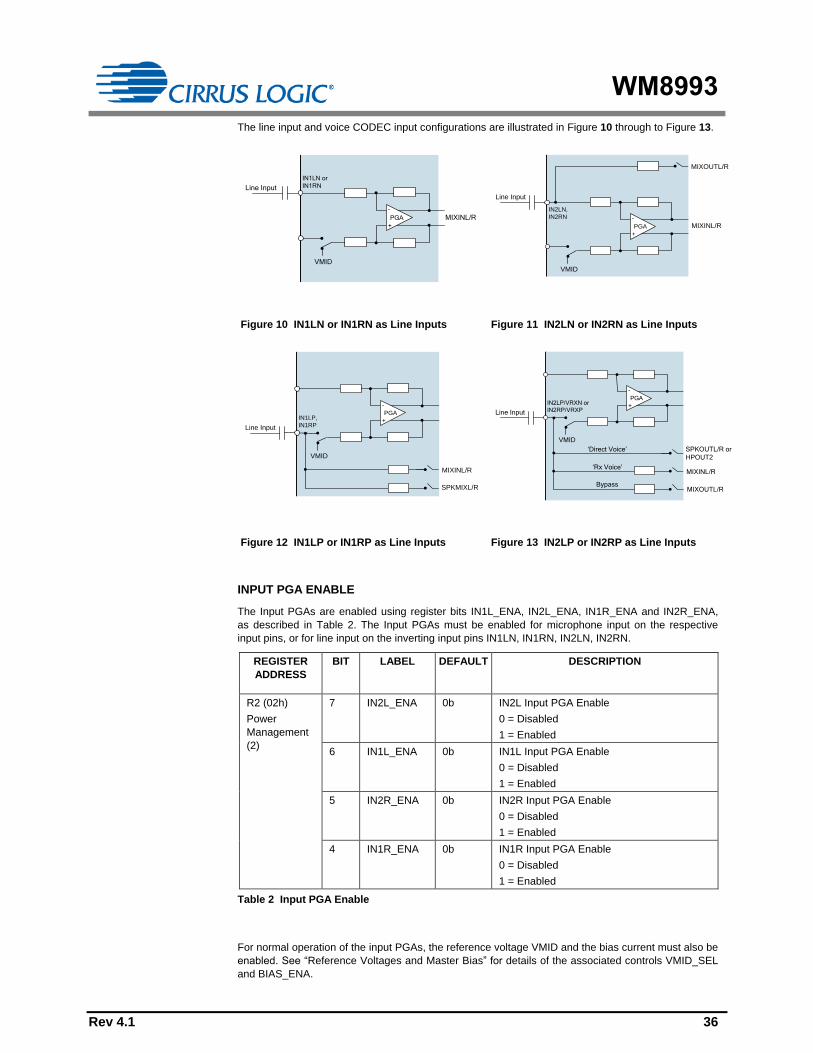
WM8993
Rev 4.1 36
The line input and voice CODEC input configurations are illustrated in Figure 10 through to Figure 13.
MIXINL/R
+
-
PGA
VMID
IN1LN or
IN1RN Line Input
+
-
PGA
VMID
IN2LN,
IN2RN
Line Input
MIXINL/R
MIXOUTL/R
Figure 10 IN1LN or IN1RN as Line Inputs Figure 11 IN2LN or IN2RN as Line Inputs
+
-
PGA
VMID
IN1LP,
IN1RPLine Input
MIXINL/R
SPKMIXL/R
+
-
PGA
VMID
IN2LP/VRXN or
IN2RP/VRXPLine Input
MIXINL/R
‘Direct Voice’
‘Rx Voice’
MIXOUTL/RBypass
SPKOUTL/R or
HPOUT2
Figure 12 IN1LP or IN1RP as Line Inputs Figure 13 IN2LP or IN2RP as Line Inputs
INPUT PGA ENABLE
The Input PGAs are enabled using register bits IN1L_ENA, IN2L_ENA, IN1R_ENA and IN2R_ENA,
as described in Table 2. The Input PGAs must be enabled for microphone input on the respective
input pins, or for line input on the inverting input pins IN1LN, IN1RN, IN2LN, IN2RN.
REGISTER
ADDRESS
BIT LABEL DEFAULT DESCRIPTION
R2 (02h)
Power
Management
(2)
7 IN2L_ENA 0b IN2L Input PGA Enable
0 = Disabled
1 = Enabled
6 IN1L_ENA 0b IN1L Input PGA Enable
0 = Disabled
1 = Enabled
5 IN2R_ENA 0b IN2R Input PGA Enable
0 = Disabled
1 = Enabled
4 IN1R_ENA 0b IN1R Input PGA Enable
0 = Disabled
1 = Enabled
Table 2 Input PGA Enable
For normal operation of the input PGAs, the reference voltage VMID and the bias current must also be
enabled. See “Reference Voltages and Master Bias” for details of the associated controls VMID_SEL
and BIAS_ENA.
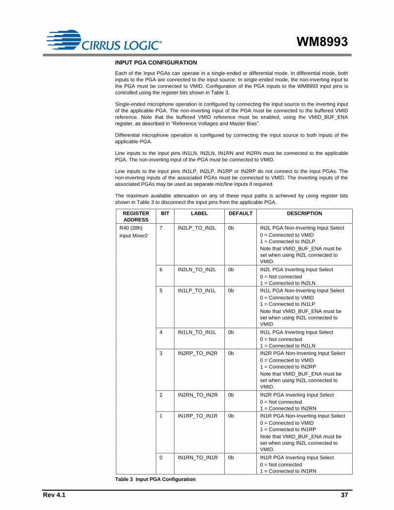
WM8993
Rev 4.1 37
INPUT PGA CONFIGURATION
Each of the Input PGAs can operate in a single-ended or differential mode. In differential mode, both
inputs to the PGA are connected to the input source. In single-ended mode, the non-inverting input to
the PGA must be connected to VMID. Configuration of the PGA inputs to the WM8993 input pins is
controlled using the register bits shown in Table 3.
Single-ended microphone operation is configured by connecting the input source to the inverting input
of the applicable PGA. The non-inverting input of the PGA must be connected to the buffered VMID
reference. Note that the buffered VMID reference must be enabled, using the VMID_BUF_ENA
register, as described in “Reference Voltages and Master Bias”.
Differential microphone operation is configured by connecting the input source to both inputs of the
applicable PGA.
Line inputs to the input pins IN1LN, IN2LN, IN1RN and IN2RN must be connected to the applicable
PGA. The non-inverting input of the PGA must be connected to VMID.
Line inputs to the input pins IN1LP, IN2LP, IN1RP or IN2RP do not connect to the input PGAs. The
non-inverting inputs of the associated PGAs must be connected to VMID. The inverting inputs of the
associated PGAs may be used as separate mic/line inputs if required.
The maximum available attenuation on any of these input paths is achieved by using register bits
shown in Table 3 to disconnect the input pins from the applicable PGA.
REGISTER
ADDRESS
BIT LABEL DEFAULT DESCRIPTION
R40 (28h)
Input Mixer2
7 IN2LP_TO_IN2L 0b IN2L PGA Non-Inverting Input Select
0 = Connected to VMID
1 = Connected to IN2LP
Note that VMID_BUF_ENA must be
set when using IN2L connected to
VMID.
6 IN2LN_TO_IN2L 0b IN2L PGA Inverting Input Select
0 = Not connected
1 = Connected to IN2LN
5 IN1LP_TO_IN1L 0b IN1L PGA Non-Inverting Input Select
0 = Connected to VMID
1 = Connected to IN1LP
Note that VMID_BUF_ENA must be
set when using IN2L connected to
VMID.
4 IN1LN_TO_IN1L 0b IN1L PGA Inverting Input Select
0 = Not connected
1 = Connected to IN1LN
3 IN2RP_TO_IN2R 0b IN2R PGA Non-Inverting Input Select
0 = Connected to VMID
1 = Connected to IN2RP
Note that VMID_BUF_ENA must be
set when using IN2L connected to
VMID.
2 IN2RN_TO_IN2R 0b IN2R PGA Inverting Input Select
0 = Not connected
1 = Connected to IN2RN
1 IN1RP_TO_IN1R 0b IN1R PGA Non-Inverting Input Select
0 = Connected to VMID
1 = Connected to IN1RP
Note that VMID_BUF_ENA must be
set when using IN2L connected to
VMID.
0 IN1RN_TO_IN1R 0b IN1R PGA Inverting Input Select
0 = Not connected
1 = Connected to IN1RN
Table 3 Input PGA Configuration

WM8993
Rev 4.1 38
INPUT PGA VOLUME CONTROL
Each of the four Input PGAs has an independently controlled gain range of -16.5dB to +30dB in 1.5dB
steps. The gains on the inverting and non-inverting inputs to the PGAs are always equal. Each Input
PGA can be independently muted using the PGA mute bits as described in Table 4, with maximum
mute attenuation achieved by simultaneously disconnecting the corresponding inputs described in
Table 3.
To prevent "zipper noise", a zero-cross function is provided on the input PGAs. When this feature is
enabled, volume updates will not take place until a zero-crossing is detected. In the case of a long
period without zero-crossings, a timeout function is provided. When the zero-cross function is
enabled, the volume will update after the timeout period if no earlier zero-cross has occurred. The
timeout clock is enabled using TOCLK_ENA, the timeout period is set by TOCLK_RATE. See
“Clocking and Sample Rates” for more information on these fields.
The IN1_VU and IN2_VU bits control the loading of the input PGA volume data. When IN1_VU and
IN2_VU are set to 0, the PGA volume data will be loaded into the respective control register, but will
not actually change the gain setting. The IN1L and IN1R volume settings are both updated when a 1
is written to IN1_VU; the IN2L and IN2R volume settings are both updated when a 1 is written to
IN2_VU. This makes it possible to update the gain of the left and right signal paths simultaneously.
The Input PGA Volume Control register fields are described in Table 4 and Table 5.
REGISTER
ADDRESS
BIT LABEL DEFAULT DESCRIPTION
R24 (18h)
Left Line Input
1&2 Volume
8 IN1_VU N/A Input PGA Volume Update
Writing a 1 to this bit will cause IN1L and
IN1R input PGA volumes to be updated
simultaneously
7 IN1L_MUTE 1b IN1L PGA Mute
0 = Disable Mute
1 = Enable Mute
6 IN1L_ZC 0b IN1L PGA Zero Cross Detector
0 = Change gain immediately
1 = Change gain on zero cross only
4:0 IN1L_VOL
[4:0]
01011b
(0dB)
IN1L Volume
-16.5dB to +30dB in 1.5dB steps
(See Table 5 for volume range)
R25 (19h)
Left Line Input
3&4 Volume
8 IN2_VU N/A Input PGA Volume Update
Writing a 1 to this bit will cause IN2L and
IN2R input PGA volumes to be updated
simultaneously
7 IN2L_MUTE 1b IN2L PGA Mute
0 = Disable Mute
1 = Enable Mute
6 IN2L_ZC 0b IN2L PGA Zero Cross Detector
0 = Change gain immediately
1 = Change gain on zero cross only
4:0 IN2L_VOL
[4:0]
01011b
(0dB)
IN2L Volume
-16.5dB to +30dB in 1.5dB steps
(See Table 5 for volume range)
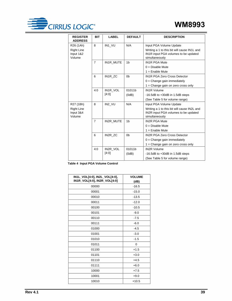
WM8993
Rev 4.1 39
REGISTER
ADDRESS
BIT LABEL DEFAULT DESCRIPTION
R26 (1Ah)
Right Line
Input 1&2
Volume
8 IN1_VU N/A Input PGA Volume Update
Writing a 1 to this bit will cause IN1L and
IN1R input PGA volumes to be updated
simultaneously
7 IN1R_MUTE 1b IN1R PGA Mute
0 = Disable Mute
1 = Enable Mute
6 IN1R_ZC 0b IN1R PGA Zero Cross Detector
0 = Change gain immediately
1 = Change gain on zero cross only
4:0 IN1R_VOL
[4:0]
01011b
(0dB)
IN1R Volume
-16.5dB to +30dB in 1.5dB steps
(See Table 5 for volume range)
R27 (1Bh)
Right Line
Input 3&4
Volume
8 IN2_VU N/A Input PGA Volume Update
Writing a 1 to this bit will cause IN2L and
IN2R input PGA volumes to be updated
simultaneously
7 IN2R_MUTE 1b IN2R PGA Mute
0 = Disable Mute
1 = Enable Mute
6 IN2R_ZC 0b IN2R PGA Zero Cross Detector
0 = Change gain immediately
1 = Change gain on zero cross only
4:0 IN2R_VOL
[4:0]
01011b
(0dB)
IN2R Volume
-16.5dB to +30dB in 1.5dB steps
(See Table 5 for volume range)
Table 4 Input PGA Volume Control
IN1L_VOL[4:0], IN2L_VOL[4:0],
IN1R_VOL[4:0], IN2R_VOL[4:0]
VOLUME
(dB)
00000 -16.5
00001 -15.0
00010 -13.5
00011 -12.0
00100 -10.5
00101 -9.0
00110 -7.5
00111 -6.0
01000 -4.5
01001 -3.0
01010 -1.5
01011 0
01100 +1.5
01101 +3.0
01110 +4.5
01111 +6.0
10000 +7.5
10001 +9.0
10010 +10.5

WM8993
Rev 4.1 40
IN1L_VOL[4:0], IN2L_VOL[4:0],
IN1R_VOL[4:0], IN2R_VOL[4:0]
VOLUME
(dB)
10011 +12.0
10100 +13.5
10101 +15.0
10110 +16.5
10111 +18.0
11000 +19.5
11001 +21.0
11010 +22.5
11011 +24.0
11100 +25.5
11101 +27.0
11110 +28.5
11111 +30.0
Table 5 Input PGA Volume Range
INPUT MIXER ENABLE
The WM8993 has two analogue input mixers which allow the Input PGAs and Line Inputs to be
combined in a number of ways and output to the ADCs, Output Mixers, or directly to the output drivers
via bypass paths.
The input mixers MIXINL and MIXINR are enabled by the MIXINL_ENA and MIXINR_ENA register
bits, as described in Table 6. These control bits also enable the RXVOICE input path, described in the
following section.
REGISTER
ADDRESS
BIT LABEL DEFAULT DESCRIPTION
R2 (02h)
Power
Management
(2)
9 MIXINL_ENA 0b Left Input Mixer Enable
(Enables MIXINL and RXVOICE input to
MIXINL)
0 = Disabled
1 = Enabled
8 MIXINR_ENA 0b Right Input Mixer Enable
(Enables MIXINR and RXVOICE input to
MIXINR)
0 = Disabled
1 = Enabled
Table 6 Input Mixer Enable
INPUT MIXER CONFIGURATION AND VOLUME CONTROL
The left and right channel input mixers MIXINL and MIXINR can be configured to take input from up to
five sources:
1. IN1L or IN1R Input PGA
2. IN2L or IN2R Input PGA
3. IN1LP or IN1RP pin (PGA bypass)
4. RXVOICE mono differential input from IN2LP/VRXN and IN2RP/VRXP
5. MIXOUTL or MIXOUTR Output Mixer (Record path)

WM8993
Rev 4.1 41
The Input Mixer configuration and volume controls are described in Table 7 for the Left input mixer
(MIXINL) and Table 8 for the Right input mixer (MIXINR). The signal levels from the Input PGAs may
be set to Mute, 0dB or 30dB boost. Gain controls for the PGA bypass, RXVOICE and Record paths
provide adjustment from -12dB to +6dB in 3dB steps.
To prevent pop noise, it is recommended that gain and mute controls for the input mixers are not
modified while the signal paths are active. If volume control is required on these signal paths, it is
recommended that this is implemented using the input PGA volume controls or the ADC volume
controls. The ADC volume controls are described in the “Analogue to Digital Converter (ADC)”
section.
REGISTER
ADDRESS
BIT LABEL DEFAULT DESCRIPTION
R41 (29h)
Input Mixer3
8 IN2L_TO_MIXINL 0b IN2L PGA Output to MIXINL Mute
0 = Mute
1 = Un-Mute
7 IN2L_MIXINL_VOL 0b IN2L PGA Output to MIXINL Gain
0 = 0dB
1 = +30dB
5 IN1L_TO_MIXINL 0b IN1L PGA Output to MIXINL Mute
0 = Mute
1 = Un-Mute
4 IN1L_MIXINL_VOL 0b IN1L PGA Output to MIXINL Gain
0 = 0dB
1 = +30dB
2:0 MIXOUTL_MIXINL_VOL
[2:0]
000b
(Mute)
Record Path MIXOUTL to MIXINL
Gain and Mute
000 = Mute
001 = -12dB
010 = -9dB
011 = -6dB
100 = -3dB
101 = 0dB
110 = +3dB
111 = +6dB
R43 (2Bh)
Input Mixer5
8:6 IN1LP_MIXINL_VOL
[2:0]
000b
(Mute)
IN1LP Pin (PGA Bypass) to
MIXINL Gain and Mute
000 = Mute
001 = -12dB
010 = -9dB
011 = -6dB
100 = -3dB
101 = 0dB
110 = +3dB
111 = +6dB
2:0 VRX_MIXINL_VOL
[2:0]
000b
(Mute)
RXVOICE (VRXN/VRXP)
Differential Input to MIXINL Gain
and Mute
000 = Mute
001 = -12dB
010 = -9dB
011 = -6dB
100 = -3dB
101 = 0dB
110 = +3dB
111 = +6dB
Table 7 Left Input Mixer (MIXINL) Volume Control
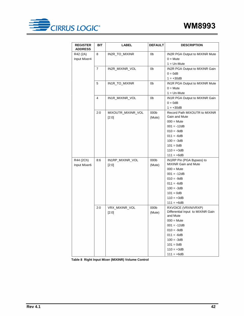
WM8993
Rev 4.1 42
REGISTER
ADDRESS
BIT LABEL DEFAULT DESCRIPTION
R42 (2A)
Input Mixer4
8 IN2R_TO_MIXINR 0b IN2R PGA Output to MIXINR Mute
0 = Mute
1 = Un-Mute
7 IN2R_MIXINR_VOL 0b IN2R PGA Output to MIXINR Gain
0 = 0dB
1 = +30dB
5 IN1R_TO_MIXINR 0b IN1R PGA Output to MIXINR Mute
0 = Mute
1 = Un-Mute
4 IN1R_MIXINR_VOL 0b IN1R PGA Output to MIXINR Gain
0 = 0dB
1 = +30dB
2:0 MIXOUTR_MIXINR_VOL
[2:0]
000b
(Mute)
Record Path MIXOUTR to MIXINR
Gain and Mute
000 = Mute
001 = -12dB
010 = -9dB
011 = -6dB
100 = -3dB
101 = 0dB
110 = +3dB
111 = +6dB
R44 (2Ch)
Input Mixer6
8:6 IN1RP_MIXINR_VOL
[2:0]
000b
(Mute)
IN1RP Pin (PGA Bypass) to
MIXINR Gain and Mute
000 = Mute
001 = -12dB
010 = -9dB
011 = -6dB
100 = -3dB
101 = 0dB
110 = +3dB
111 = +6dB
2:0 VRX_MIXINR_VOL
[2:0]
000b
(Mute)
RXVOICE (VRXN/VRXP)
Differential Input to MIXINR Gain
and Mute
000 = Mute
001 = -12dB
010 = -9dB
011 = -6dB
100 = -3dB
101 = 0dB
110 = +3dB
111 = +6dB
Table 8 Right Input Mixer (MIXINR) Volume Control

WM8993
Rev 4.1 43
ANALOGUE TO DIGITAL CONVERTER (ADC)
The WM8993 uses stereo 24-bit, 128x oversampled sigma-delta ADCs. The use of multi-bit feedback
and high oversampling rates reduces the effects of jitter and high frequency noise. An oversample
rate of 64x can also be supported - see “Clocking and Sample Rates” for details. The ADC full scale
input level is proportional to AVDD1 - see “Electrical Characteristics”. Any input signal greater than full
scale may overload the ADC and cause distortion.
The ADCs are enabled by the ADCL_ENA and ADCR_ENA register bits.
REGISTER
ADDRESS
BIT LABEL DEFAULT DESCRIPTION
R2 (02h)
Power
Management (2)
1 ADCL_ENA 0 Left ADC Enable
0 = ADC disabled
1 = ADC enabled
0 ADCR_ENA 0 Right ADC Enable
0 = ADC disabled
1 = ADC enabled
Table 9 ADC Enable Control
ADC DIGITAL VOLUME CONTROL
The output of the ADCs can be digitally amplified or attenuated over a range from -71.625dB to
+17.625dB in 0.375dB steps. The volume of each channel can be controlled separately. The gain for a
given eight-bit code X is given by:
0.375 (X-192) dB for 1 X 239; MUTE for X = 0 +17.625dB for 239 X 255
The ADC_VU bit controls the loading of digital volume control data. When ADC_VU is set to 0, the
ADCL_VOL or ADCR_VOL control data will be loaded into the respective control register, but will not
actually change the digital gain setting. Both left and right gain settings are updated when a 1 is
written to ADC_VU. This makes it possible to update the gain of both channels simultaneously.
REGISTER
ADDRESS
BIT LABEL DEFAULT DESCRIPTION
R15 (0Fh)
Left ADC
Digital Volume
8 ADC_VU N/A ADC Volume Update
Writing a 1 to this bit will cause left
and right ADC volume to be updated
simultaneously
7:0 ADCL_VOL
[7:0]
1100_0000
(0dB)
Left ADC Digital Volume
00h = MUTE
01h = -71.625dB
… (0.375dB steps)
EFh = +17.625dB
(See Table 11 for volume range)
R16 (10h)
Right ADC
Digital Volume
8 ADC_VU N/A ADC Volume Update
Writing a 1 to this bit will cause left
and right ADC volume to be updated
simultaneously
7:0 ADCR_VOL
[7:0]
1100_0000
(0dB)
Right ADC Digital Volume
00h = MUTE
01h = -71.625dB
… (0.375dB steps)
EFh = +17.625dB
(See Table 11 for volume range)
Table 10 ADC Digital Volume Control

WM8993
Rev 4.1 44
ADCL_VOL or
ADCR_VOL Volume (dB)
ADCL_VOL or
ADCR_VOL Volume (dB)
ADCL_VOL or
ADCR_VOL Volume (dB)
ADCL_VOL or
ADCR_VOL Volume (dB)
0h MUTE 40h -48.000 80h -24.000 C0h 0.000
1h -71.625 41h -47.625 81h -23.625 C1h 0.375
2h -71.250 42h -47.250 82h -23.250 C2h 0.750
3h -70.875 43h -46.875 83h -22.875 C3h 1.125
4h -70.500 44h -46.500 84h -22.500 C4h 1.500
5h -70.125 45h -46.125 85h -22.125 C5h 1.875
6h -69.750 46h -45.750 86h -21.750 C6h 2.250
7h -69.375 47h -45.375 87h -21.375 C7h 2.625
8h -69.000 48h -45.000 88h -21.000 C8h 3.000
9h -68.625 49h -44.625 89h -20.625 C9h 3.375
Ah -68.250 4Ah -44.250 8Ah -20.250 CAh 3.750
Bh -67.875 4Bh -43.875 8Bh -19.875 CBh 4.125
Ch -67.500 4Ch -43.500 8Ch -19.500 CCh 4.500
Dh -67.125 4Dh -43.125 8Dh -19.125 CDh 4.875
Eh -66.750 4Eh -42.750 8Eh -18.750 CEh 5.250
Fh -66.375 4Fh -42.375 8Fh -18.375 CFh 5.625
10h -66.000 50h -42.000 90h -18.000 D0h 6.000
11h -65.625 51h -41.625 91h -17.625 D1h 6.375
12h -65.250 52h -41.250 92h -17.250 D2h 6.750
13h -64.875 53h -40.875 93h -16.875 D3h 7.125
14h -64.500 54h -40.500 94h -16.500 D4h 7.500
15h -64.125 55h -40.125 95h -16.125 D5h 7.875
16h -63.750 56h -39.750 96h -15.750 D6h 8.250
17h -63.375 57h -39.375 97h -15.375 D7h 8.625
18h -63.000 58h -39.000 98h -15.000 D8h 9.000
19h -62.625 59h -38.625 99h -14.625 D9h 9.375
1Ah -62.250 5Ah -38.250 9Ah -14.250 DAh 9.750
1Bh -61.875 5Bh -37.875 9Bh -13.875 DBh 10.125
1Ch -61.500 5Ch -37.500 9Ch -13.500 DCh 10.500
1Dh -61.125 5Dh -37.125 9Dh -13.125 DDh 10.875
1Eh -60.750 5Eh -36.750 9Eh -12.750 DEh 11.250
1Fh -60.375 5Fh -36.375 9Fh -12.375 DFh 11.625
20h -60.000 60h -36.000 A0h -12.000 E0h 12.000
21h -59.625 61h -35.625 A1h -11.625 E1h 12.375
22h -59.250 62h -35.250 A2h -11.250 E2h 12.750
23h -58.875 63h -34.875 A3h -10.875 E3h 13.125
24h -58.500 64h -34.500 A4h -10.500 E4h 13.500
25h -58.125 65h -34.125 A5h -10.125 E5h 13.875
26h -57.750 66h -33.750 A6h -9.750 E6h 14.250
27h -57.375 67h -33.375 A7h -9.375 E7h 14.625
28h -57.000 68h -33.000 A8h -9.000 E8h 15.000
29h -56.625 69h -32.625 A9h -8.625 E9h 15.375
2Ah -56.250 6Ah -32.250 AAh -8.250 EAh 15.750
2Bh -55.875 6Bh -31.875 ABh -7.875 EBh 16.125
2Ch -55.500 6Ch -31.500 ACh -7.500 ECh 16.500
2Dh -55.125 6Dh -31.125 ADh -7.125 EDh 16.875
2Eh -54.750 6Eh -30.750 AEh -6.750 EEh 17.250
2Fh -54.375 6Fh -30.375 AFh -6.375 EFh 17.625
30h -54.000 70h -30.000 B0h -6.000 F0h 17.625
31h -53.625 71h -29.625 B1h -5.625 F1h 17.625
32h -53.250 72h -29.250 B2h -5.250 F2h 17.625
33h -52.875 73h -28.875 B3h -4.875 F3h 17.625
34h -52.500 74h -28.500 B4h -4.500 F4h 17.625
35h -52.125 75h -28.125 B5h -4.125 F5h 17.625
36h -51.750 76h -27.750 B6h -3.750 F6h 17.625
37h -51.375 77h -27.375 B7h -3.375 F7h 17.625
38h -51.000 78h -27.000 B8h -3.000 F8h 17.625
39h -50.625 79h -26.625 B9h -2.625 F9h 17.625
3Ah -50.250 7Ah -26.250 BAh -2.250 FAh 17.625
3Bh -49.875 7Bh -25.875 BBh -1.875 FBh 17.625
3Ch -49.500 7Ch -25.500 BCh -1.500 FCh 17.625
3Dh -49.125 7Dh -25.125 BDh -1.125 FDh 17.625
3Eh -48.750 7Eh -24.750 BEh -0.750 FEh 17.625
3Fh -48.375 7Fh -24.375 BFh -0.375 FFh 17.625
Table 11 ADC Digital Volume Range

WM8993
Rev 4.1 45
HIGH PASS FILTER
A digital high pass filter is applied by default to the ADC path to remove DC offsets. This filter can also
be programmed to remove low frequency noise in voice applications (e.g. wind noise or mechanical
vibration). This filter is controlled using the ADC_HPF and ADC_HPF_CUT register bits.
In hi-fi mode the high pass filter is optimised for removing DC offsets without degrading the bass
response and has a cut-off frequency of 3.7Hz at fs=44.1kHz.
In voice mode the high pass filter is optimised for voice communication and it is recommended to
program the cut-off frequency below 300Hz (e.g. ADC_HPF_CUT=11 at fs=8kHz or
ADC_HPF_CUT=10 at fs=16kHz).
REGISTER
ADDRESS
BIT LABEL DEFAULT DESCRIPTION
R14 (0Eh)
ADC
CTRL
8 ADC_HPF 1 ADC Digital High Pass Filter Enable
0 = disabled
1 = enabled
6:5 ADC_HPF_CUT
[1:0]
00 ADC Digital High Pass Filter Cut-Off
Frequency (fc)
00 = Hi-fi mode (fc=4Hz at fs=48kHz)
01 = Voice mode 1 (fc=127Hz at fs=16kHz)
10 = Voice mode 2 (fc=130Hz at fs=8kHz)
11 = Voice mode 3 (fc=267Hz at fs=8kHz)
(Note: fc scales with sample rate. See
Table 13 for cut-off frequencies at all
supported sample rates)
Table 12 ADC High Pass Filter Control Registers
Sample
Frequency
(kHz)
CUT-OFF FREQUENCY (Hz)
ADC_HPF_CUT
=00
ADC_HPF_CUT
=01
ADC_HPF_CUT
=10
ADC_HPF_CUT
=11
8.000 0.7 64 130 267
11.025 0.9 88 178 367
16.000 1.3 127 258 532
22.050 1.9 175 354 733
24.000 2.0 190 386 798
32.000 2.7 253 514 1063
44.100 3.7 348 707 1464
48.000 4.0 379 770 1594
Table 13 ADC High Pass Filter Cut-Off Frequencies
The high pass filter characteristics are shown in the "Digital Filter Characteristics" section.

WM8993
Rev 4.1 46
DIGITAL MIXING
The ADC and DAC data can be combined in various ways to support a range of different usage
modes.
Data from either of the two ADCs can be routed to either the left or the right channel of the digital
audio interface. In addition, data from either of the digital audio interface channels can be routed to
either the left or the right DAC. See "Digital Audio Interface" for more information on the audio
interface.
The WM8993 provides a Dynamic Range Control (DRC) feature, which can apply compression and
gain adjustment in the digital domain to either the ADC or DAC signal path. This is effective in
controlling signal levels under conditions where input amplitude is unknown or varies over a wide
range.
The DACs can be configured as a mono mix of the two audio channels. Digital sidetone from the
ADCs can also be selectively mixed into the DAC output path.
DIGITAL MIXING PATHS
Figure 14 shows the digital mixing paths available in the WM8993 digital core.
AD
CD
AT
BC
LK
DA
CD
AT
LR
CL
K
DAC L
DAC R
ADC L
ADC R
ReTune Mobile
Parametric
Equalizer
L R
R L
L/R SWAP
Dynamic Range
Controller
Dynamic Range Control
(DRC) available on ADC
or DAC channels, not both.
Dynamic Range
Controller
+
DIGITAL AUDIO
INTERFACEA-law and -law Support
TDM Support
MONO MIX
+
L R
R L
AIFADCL_SRC
AIFADCR_SRC
ADCL_DATINV
ADCR_DATINV
AIFDACL_SRC
AIFDACR_SRC
DACL_DATINV
DACR_DATINV
DAC_VU
DACL_VOL[7:0]
DACR_VOL[7:0]
DAC_MUTE
DAC_BOOST[1:0]
DAC_MUTERATE
DAC_UNMUTE_RAMP
ADC_VU
ADCL_VOL[7:0]
ADCR_VOL[7:0]
ADCL_ENA
ADCR_ENA
DACL_ENA
DACR_ENA
DEEMPH[1:0]
DAC_COMP
DAC_COMPMODE
ADC_COMP
ADC_COMPMODE
AIFDAC_TDM
AIFDAC_TDM_CHAN
AIFADC_TDM
AIFADC_TDM_CHAN
AIF_WL[1:0]
AIF_FMT[1:0]
LOOPBACK
ADC_HPF
ADC_HPF_CUT[1:0]
ADCL_DAC_SVOL[3:0]
ADCR_DAC_SVOL[3:0]
DAC_SB_FILT
DAC_MONO
ADC_TO_DACL[1:0]
ADC_TO_DACR[1:0]
Figure 14 Digital Mixing Paths

WM8993
Rev 4.1 47
The polarity of each ADC output signal can be changed under software control using the ADCL_DATINV and
ADCR_DATINV register bits. The AIFADCL_SRC and AIFADCR_SRC register bits may be used to select
which ADC is used for the left and right digital audio interface data. These register bits are described in Table
14.
REGISTER
ADDRESS
BIT LABEL DEFAULT DESCRIPTION
R4 (04h)
Audio
Interface (1)
15 AIFADCL_SRC 0 Left Digital Audio interface source
0 = Left ADC data is output on left channel
1 = Right ADC data is output on left channel
14 AIFADCR_SRC 1 Right Digital Audio interface source
0 = Left ADC data is output on right channel
1 = Right ADC data is output on right channel
R14 (0Eh)
ADC CTRL
1 ADCL_DATINV 0 Left ADC Invert
0 = Left ADC output not inverted
1 = Left ADC output inverted
0 ADCR_DATINV 0 Right ADC Invert
0 = Right ADC output not inverted
1 = Right ADC output inverted
Table 14 ADC Routing and Control
The input data source for each DAC can be changed under software control using register bits
AIFDACL_SRC and AIFDACR_SRC. The polarity of each DAC input may also be modified using
register bits DACL_DATINV and DACR_DATINV. These register bits are described in Table 15.
REGISTER
ADDRESS
BIT LABEL DEFAULT DESCRIPTION
R5 (05h)
Audio
Interface (2)
15 AIFDACL_SRC 0 Left DAC Data Source Select
0 = Left DAC outputs left interface data
1 = Left DAC outputs right interface data
14 AIFDACR_SRC 1 Right DAC Data Source Select
0 = Right DAC outputs left interface data
1 = Right DAC outputs right interface data
R10 (0Ah)
DAC CTRL
1 DACL_DATINV 0 Left DAC Invert
0 = Left DAC output not inverted
1 = Left DAC output inverted
0 DACR_DATINV 0 Right DAC Invert
0 = Right DAC output not inverted
1 = Right DAC output inverted
Table 15 DAC Routing and Control

WM8993
Rev 4.1 48
DAC INTERFACE VOLUME BOOST
A digital gain function is available at the audio interface to boost the DAC volume when a small signal
is received on DACDAT. This is controlled using register bits DAC_BOOST[1:0]. To prevent clipping
at the DAC input, this function should not be used when the boosted DAC data is expected to be
greater than 0dBFS.
REGISTER
ADDRESS
BIT LABEL DEFAULT DESCRIPTION
R5 (05h)
Audio
Interface (2)
11:10 DAC_BOOST
[1:0]
00 DAC Input Volume Boost
00 = 0dB
01 = +6dB (Input data must not
exceed -6dBFS)
10 = +12dB (Input data must not
exceed -12dBFS)
11 = +18dB (Input data must not
exceed -18dBFS)
Table 16 DAC Interface Volume Boost
DIGITAL SIDETONE
A digital sidetone is available when ADCs and DACs are operating at the same sample rate. Digital
data from either left or right ADC can be mixed with the audio interface data on the left and right DAC
channels. Sidetone data is taken from the ADC high pass filter output, to reduce low frequency noise
in the sidetone (e.g. wind noise or mechanical vibration).
When using the digital sidetone, it is recommended that the ADCs are enabled before un-muting the
DACs to prevent pop noise. The DAC volumes and sidetone volumes should be set to an appropriate
level to avoid clipping at the DAC input.
The digital sidetone is controlled as shown in Table 17.
REGISTER
ADDRESS
BIT LABEL DEFAULT DESCRIPTION
R13 (0Dh)
Digital Side
Tone
12:9 ADCL_DAC_SVOL
[3:0]
0000 Left Digital Sidetone Volume
0000 = -36dB
0001 = -33dB
…. (3dB steps)
1011 = -3dB
1100 = 0dB
(See Table 18 for volume range)
8:5 ADCR_DAC_SVOL
[3:0]
0000 Right Digital Sidetone Volume
0000 = -36dB
0001 = -33dB
…. (3dB steps)
1011 = -3dB
1100 = 0dB
(See Table 18 for volume range)
3:2 ADCL_TO_DACL
[1:0]
00 Left DAC Digital Sidetone Source
00 = No sidetone
01 = Left ADC
10 = Right ADC
11 = Reserved
1:0 ADC_TO_DACR
[1:0]
00 Right DAC Digital Sidetone Source
00 = No sidetone
01 = Left ADC
10 = Right ADC
11 = Reserved
Table 17 Digital Sidetone Control

WM8993
Rev 4.1 49
ADCL_DAC_SVOL or
ADCR_DAC_SVOL
SIDETONE
VOLUME
(dB)
0000 -36
0001 -33
0010 -30
0011 -27
0100 -24
0101 -21
0110 -18
0111 -15
1000 -12
1001 -9
1010 -6
1011 -3
1100 0
1101 0
1110 0
1111 0
Table 18 Digital Sidetone Volume
DYNAMIC RANGE CONTROL (DRC)
The dynamic range controller (DRC) is a circuit which can be enabled in the digital data path of either
the ADCs or the DACs. The function of the DRC is to adjust the signal gain in conditions where the
input amplitude is unknown or varies over a wide range, e.g. when recording from microphones built
into a handheld system. The DRC can apply Compression and Automatic Level Control to the signal
path. It incorporates ‘anti-clip’ and ‘quick release’ features for handling transients in order to improve
intelligibility in the presence of loud impulsive noises.
The DRC is enabled as shown in Table 19. It can be enabled in the ADC digital path or in the DAC
digital path, under the control of the DRC_DAC_PATH register bit. Note that the DRC can only be
active in one of these paths at any time.
REGISTER
ADDRESS
BIT LABEL DEFAULT DESCRIPTION
R123 (7Bh)
DRC Control 1
15 DRC_ENA 0 DRC enable
0 = disabled
1 = enabled
14 DRC_DAC_PAT
H
0 DRC path select
0 = ADC path
1 = DAC path
Table 19 DRC Enable
COMPRESSION/LIMITING CAPABILITIES
The DRC supports two different compression regions, specified by R0 and R1, separated by a “knee”
at input amplitude T. For signals above the knee, the compression slope R0 applies; for signals below
the knee, the compression slope R1 applies.
The overall DRC compression characteristic in “steady state” (i.e. where the input amplitude is near-
constant) is illustrated in Figure 15.

WM8993
Rev 4.1 50
T
(Y0)
0dB
R0
R1
DRC Input Amplitude (dB)
DR
C O
utp
ut
Am
plit
ud
e (
dB
)
YT
“knee”
Figure 15 DRC Compression Characteristic
The slope of R0 and R1 are determined by register fields DRC_R0_SLOPE_COMP and
DRC_R1_SLOPE_COMP respectively. A slope of 1 indicates constant gain in this region. A slope less
than 1 represents compression (i.e. a change in input amplitude produces only a smaller change in
output amplitude). A slope of 0 indicates that the target output amplitude is the same across a range
of input amplitudes; this is infinite compression.
The “knee” in Figure 15 is represented by T and Y, which are determined by register fields
DRC_THRESH_COMP and DRC_AMP_COMP respectively.
Parameter Y0, the output level for a 0dB input, is not specified directly, but can be calculated from the
other parameters, using the equation
Y0 = YT – (T * R0)
The DRC Compression parameters are defined in Table 20.
REGISTER
ADDRESS
BIT LABEL DEFAULT DESCRIPTION
R124 (7Ch)
DRC Control 2
7:2 DRC_THRESH_
COMP [5:0]
000000 Compressor threshold T (dB)
000000 = 0dB
000001 = -0.75dB
000010 = -1.5dB
… (-0.75dB steps)
111100 = -45dB
111101 = Reserved
11111X = Reserved
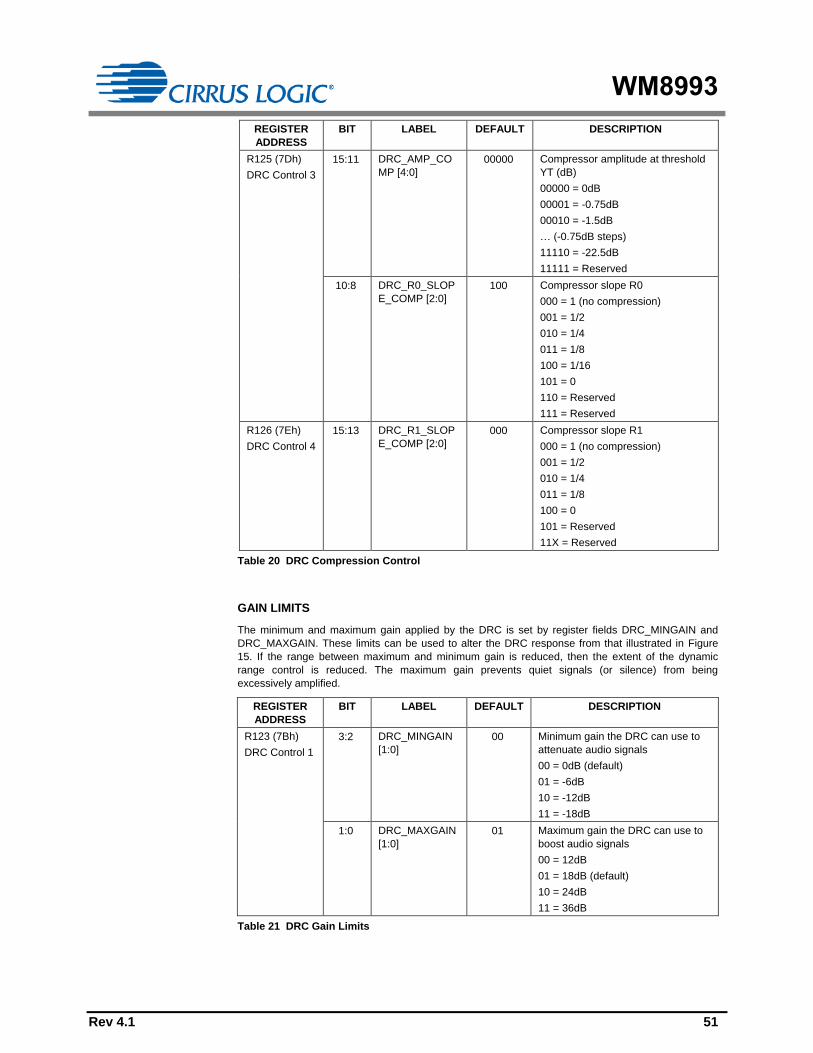
WM8993
Rev 4.1 51
REGISTER
ADDRESS
BIT LABEL DEFAULT DESCRIPTION
R125 (7Dh)
DRC Control 3
15:11 DRC_AMP_CO
MP [4:0]
00000 Compressor amplitude at threshold
YT (dB)
00000 = 0dB
00001 = -0.75dB
00010 = -1.5dB
… (-0.75dB steps)
11110 = -22.5dB
11111 = Reserved
10:8 DRC_R0_SLOP
E_COMP [2:0]
100 Compressor slope R0
000 = 1 (no compression)
001 = 1/2
010 = 1/4
011 = 1/8
100 = 1/16
101 = 0
110 = Reserved
111 = Reserved
R126 (7Eh)
DRC Control 4
15:13 DRC_R1_SLOP
E_COMP [2:0]
000 Compressor slope R1
000 = 1 (no compression)
001 = 1/2
010 = 1/4
011 = 1/8
100 = 0
101 = Reserved
11X = Reserved
Table 20 DRC Compression Control
GAIN LIMITS
The minimum and maximum gain applied by the DRC is set by register fields DRC_MINGAIN and
DRC_MAXGAIN. These limits can be used to alter the DRC response from that illustrated in Figure
15. If the range between maximum and minimum gain is reduced, then the extent of the dynamic
range control is reduced. The maximum gain prevents quiet signals (or silence) from being
excessively amplified.
REGISTER
ADDRESS
BIT LABEL DEFAULT DESCRIPTION
R123 (7Bh)
DRC Control 1
3:2 DRC_MINGAIN
[1:0]
00 Minimum gain the DRC can use to
attenuate audio signals
00 = 0dB (default)
01 = -6dB
10 = -12dB
11 = -18dB
1:0 DRC_MAXGAIN
[1:0]
01 Maximum gain the DRC can use to
boost audio signals
00 = 12dB
01 = 18dB (default)
10 = 24dB
11 = 36dB
Table 21 DRC Gain Limits
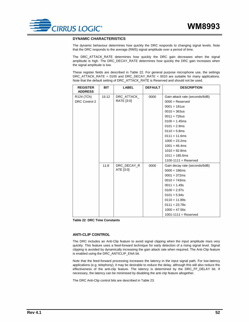
WM8993
Rev 4.1 52
DYNAMIC CHARACTERISTICS
The dynamic behaviour determines how quickly the DRC responds to changing signal levels. Note
that the DRC responds to the average (RMS) signal amplitude over a period of time.
The DRC_ATTACK_RATE determines how quickly the DRC gain decreases when the signal
amplitude is high. The DRC_DECAY_RATE determines how quickly the DRC gain increases when
the signal amplitude is low.
These register fields are described in Table 22. For general purpose microphone use, the settings
DRC_ATTACK_RATE = 0100 and DRC_DECAY_RATE = 0010 are suitable for many applications.
Note that the default setting of DRC_ATTACK_RATE is Reserved and should not be used.
REGISTER
ADDRESS
BIT LABEL DEFAULT DESCRIPTION
R124 (7Ch)
DRC Control 2
15:12 DRC_ATTACK_
RATE [3:0]
0000 Gain attack rate (seconds/6dB)
0000 = Reserved
0001 = 181us
0010 = 363us
0011 = 726us
0100 = 1.45ms
0101 = 2.9ms
0110 = 5.8ms
0111 = 11.6ms
1000 = 23.2ms
1001 = 46.4ms
1010 = 92.8ms
1011 = 185.6ms
1100-1111 = Reserved
11:8 DRC_DECAY_R
ATE [3:0]
0000 Gain decay rate (seconds/6dB)
0000 = 186ms
0001 = 372ms
0010 = 743ms
0011 = 1.49s
0100 = 2.97s
0101 = 5.94s
0110 = 11.89s
0111 = 23.78s
1000 = 47.56s
1001-1111 = Reserved
Table 22 DRC Time Constants
ANTI-CLIP CONTROL
The DRC includes an Anti-Clip feature to avoid signal clipping when the input amplitude rises very
quickly. This feature uses a feed-forward technique for early detection of a rising signal level. Signal
clipping is avoided by dynamically increasing the gain attack rate when required. The Anti-Clip feature
is enabled using the DRC_ANTICLIP_ENA bit.
Note that the feed-forward processing increases the latency in the input signal path. For low-latency
applications (e.g. telephony), it may be desirable to reduce the delay, although this will also reduce the
effectiveness of the anti-clip feature. The latency is determined by the DRC_FF_DELAY bit. If
necessary, the latency can be minimised by disabling the anti-clip feature altogether.
The DRC Anti-Clip control bits are described in Table 23.
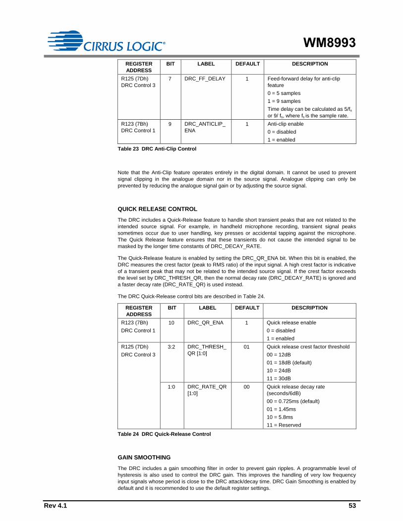
WM8993
Rev 4.1 53
REGISTER
ADDRESS
BIT LABEL DEFAULT DESCRIPTION
R125 (7Dh)
DRC Control 3
7 DRC_FF_DELAY 1 Feed-forward delay for anti-clip
feature
0 = 5 samples
1 = 9 samples
Time delay can be calculated as 5/fs
or 9/ fs, where fs is the sample rate.
R123 (7Bh)
DRC Control 1
9 DRC_ANTICLIP_
ENA
1 Anti-clip enable
0 = disabled
1 = enabled
Table 23 DRC Anti-Clip Control
Note that the Anti-Clip feature operates entirely in the digital domain. It cannot be used to prevent
signal clipping in the analogue domain nor in the source signal. Analogue clipping can only be
prevented by reducing the analogue signal gain or by adjusting the source signal.
QUICK RELEASE CONTROL
The DRC includes a Quick-Release feature to handle short transient peaks that are not related to the
intended source signal. For example, in handheld microphone recording, transient signal peaks
sometimes occur due to user handling, key presses or accidental tapping against the microphone.
The Quick Release feature ensures that these transients do not cause the intended signal to be
masked by the longer time constants of DRC_DECAY_RATE.
The Quick-Release feature is enabled by setting the DRC_QR_ENA bit. When this bit is enabled, the
DRC measures the crest factor (peak to RMS ratio) of the input signal. A high crest factor is indicative
of a transient peak that may not be related to the intended source signal. If the crest factor exceeds
the level set by DRC_THRESH_QR, then the normal decay rate (DRC_DECAY_RATE) is ignored and
a faster decay rate (DRC_RATE_QR) is used instead.
The DRC Quick-Release control bits are described in Table 24.
REGISTER
ADDRESS
BIT LABEL DEFAULT DESCRIPTION
R123 (7Bh)
DRC Control 1
10 DRC_QR_ENA 1 Quick release enable
0 = disabled
1 = enabled
R125 (7Dh)
DRC Control 3
3:2 DRC_THRESH_
QR [1:0]
01 Quick release crest factor threshold
00 = 12dB
01 = 18dB (default)
10 = 24dB
11 = 30dB
1:0 DRC_RATE_QR
[1:0]
00 Quick release decay rate
(seconds/6dB)
00 = 0.725ms (default)
01 = 1.45ms
10 = 5.8ms
11 = Reserved
Table 24 DRC Quick-Release Control
GAIN SMOOTHING
The DRC includes a gain smoothing filter in order to prevent gain ripples. A programmable level of
hysteresis is also used to control the DRC gain. This improves the handling of very low frequency
input signals whose period is close to the DRC attack/decay time. DRC Gain Smoothing is enabled by
default and it is recommended to use the default register settings.

WM8993
Rev 4.1 54
The extent of the gain smoothing filter may be adjusted or disabled using the control fields described
in Table 25.
REGISTER
ADDRESS
BIT LABEL DEFAULT DESCRIPTION
R123 (7Bh)
DRC Control 1
11 DRC_SMOOTH_
ENA
1 Gain smoothing enable
0 = disabled
1 = enabled
8 DRC_HYST_EN
A
1 Gain smoothing hysteresis enable
0 = disabled
1 = enabled
5:4 DRC_THRESH_
HYST [1:0]
01 Gain smoothing hysteresis
threshold
00 = Low
01 = Medium (recommended)
10 = High
11 = Reserved
Table 25 DRC Gain Smoothing
INITIALISATION
When the DRC is initialised, the gain is set to the level determined by the DRC_STARTUP_GAIN
register field. The default setting is 0dB, but values from -3dB to +6dB are available, as described in
Table 26.
REGISTER
ADDRESS
BIT LABEL DEFAULT DESCRIPTION
R126 (7Eh)
DRC Control 4
12:8 DRC_STARTUP_
GAIN [4:0]
00110 Initial gain at DRC startup
00000 = -18dB
00001 = -15dB
00010 = -12dB
00011 = -9dB
00100 = -6dB
00101 = -3dB
00110 = 0dB (default)
00111 = 3dB
01000 = 6dB
01001 = 9dB
01010 = 12dB
01011 = 15dB
01100 = 18dB
01101 = 21dB
01110 = 24dB
01111 = 27dB
10000 = 30dB
10001 = 33dB
10010 = 36dB
10011 to 11111 = Reserved
Table 26 DRC Initialisation
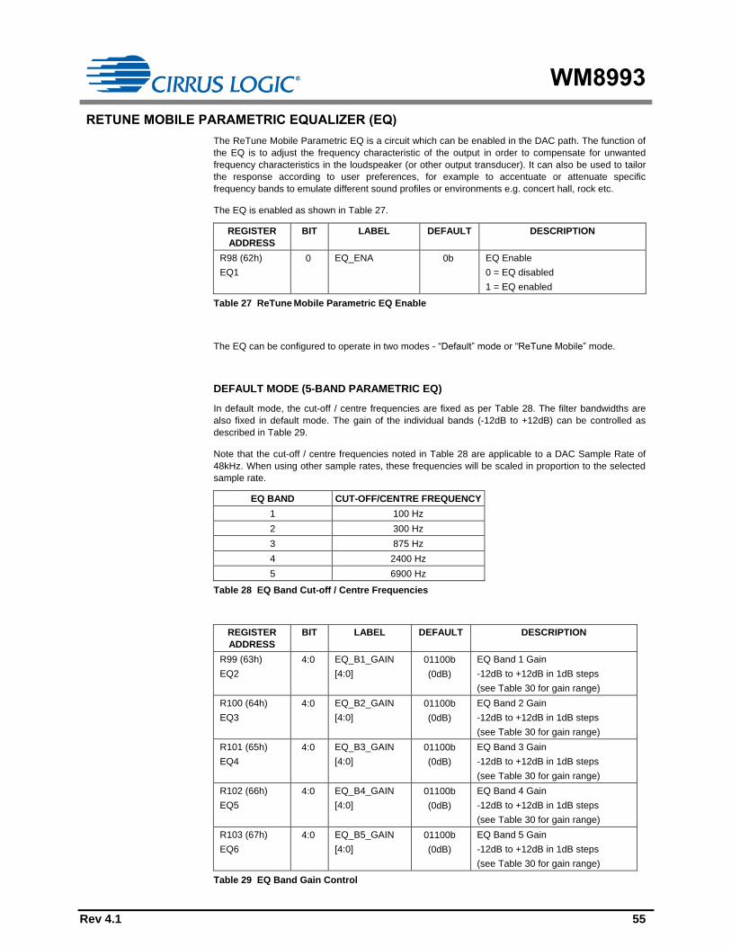
WM8993
Rev 4.1 55
RETUNE MOBILE PARAMETRIC EQUALIZER (EQ)
The ReTune Mobile Parametric EQ is a circuit which can be enabled in the DAC path. The function of
the EQ is to adjust the frequency characteristic of the output in order to compensate for unwanted
frequency characteristics in the loudspeaker (or other output transducer). It can also be used to tailor
the response according to user preferences, for example to accentuate or attenuate specific
frequency bands to emulate different sound profiles or environments e.g. concert hall, rock etc.
The EQ is enabled as shown in Table 27.
REGISTER
ADDRESS
BIT LABEL DEFAULT DESCRIPTION
R98 (62h)
EQ1
0 EQ_ENA 0b EQ Enable
0 = EQ disabled
1 = EQ enabled
Table 27 ReTune Mobile Parametric EQ Enable
The EQ can be configured to operate in two modes - “Default” mode or “ReTune Mobile” mode.
DEFAULT MODE (5-BAND PARAMETRIC EQ)
In default mode, the cut-off / centre frequencies are fixed as per Table 28. The filter bandwidths are
also fixed in default mode. The gain of the individual bands (-12dB to +12dB) can be controlled as
described in Table 29.
Note that the cut-off / centre frequencies noted in Table 28 are applicable to a DAC Sample Rate of
48kHz. When using other sample rates, these frequencies will be scaled in proportion to the selected
sample rate.
EQ BAND CUT-OFF/CENTRE FREQUENCY
1 100 Hz
2 300 Hz
3 875 Hz
4 2400 Hz
5 6900 Hz
Table 28 EQ Band Cut-off / Centre Frequencies
REGISTER
ADDRESS
BIT LABEL DEFAULT DESCRIPTION
R99 (63h)
EQ2
4:0 EQ_B1_GAIN
[4:0]
01100b
(0dB)
EQ Band 1 Gain
-12dB to +12dB in 1dB steps
(see Table 30 for gain range)
R100 (64h)
EQ3
4:0 EQ_B2_GAIN
[4:0]
01100b
(0dB)
EQ Band 2 Gain
-12dB to +12dB in 1dB steps
(see Table 30 for gain range)
R101 (65h)
EQ4
4:0 EQ_B3_GAIN
[4:0]
01100b
(0dB)
EQ Band 3 Gain
-12dB to +12dB in 1dB steps
(see Table 30 for gain range)
R102 (66h)
EQ5
4:0 EQ_B4_GAIN
[4:0]
01100b
(0dB)
EQ Band 4 Gain
-12dB to +12dB in 1dB steps
(see Table 30 for gain range)
R103 (67h)
EQ6
4:0 EQ_B5_GAIN
[4:0]
01100b
(0dB)
EQ Band 5 Gain
-12dB to +12dB in 1dB steps
(see Table 30 for gain range)
Table 29 EQ Band Gain Control

WM8993
Rev 4.1 56
EQ GAIN SETTING GAIN (DB)
00000 -12
00001 -11
00010 -10
00011 -9
00100 -8
00101 -7
00110 -6
00111 -5
01000 -4
01001 -3
01010 -2
01011 -1
01100 0
01101 +1
01110 +2
01111 +3
10000 +4
10001 +5
10010 +6
10011 +7
10100 +8
10101 +9
10110 +10
10111 +11
11000 +12
11001 to 11111 Reserved
Table 30 EQ Gain Control
RETUNE MOBILE MODE
ReTune Mobile mode provides a comprehensive facility for the user to define the cut-off/centre
frequencies and filter bandwidth for each EQ band, in addition to the gain controls already described.
This enables the EQ to be accurately customised for a specific transducer characteristic or desired
sound profile.
The EQ enable and EQ gain controls are the same as defined for the default mode. The additional
coefficients used in ReTune Mobile mode are held in registers R104 to R121. These coefficients are
derived using tools provided in WISCE™ evaluation board control software.
Please contact your local Cirrus Logic representative for more details.
EQ FILTER CHARACTERISTICS
The filter characteristics for each frequency band are shown in Figure 16 to Figure 20. These figures
show the frequency response for all available gain settings, using default cut-off/centre frequencies
and bandwidth.

WM8993
Rev 4.1 57
-15
-10
-5
0
5
10
15
1 10 100 1000 10000 100000
Frequency (Hz)
Ga
in (
dB
)
-15
-10
-5
0
5
10
15
1 10 100 1000 10000 100000
Frequency (Hz)
Ga
in (
dB
)
Figure 16 EQ Band 1 – Low Freq Shelf Filter Response Figure 17 EQ Band 2 – Peak Filter Response
-15
-10
-5
0
5
10
15
1 10 100 1000 10000 100000
Frequency (Hz)
Ga
in (
dB
)
-15
-10
-5
0
5
10
15
1 10 100 1000 10000 100000
Frequency (Hz)
Ga
in (
dB
)
Figure 18 EQ Band 3 – Peak Filter Response Figure 19 EQ Band 4 – Peak Filter Response
-15
-10
-5
0
5
10
15
1 10 100 1000 10000 100000
Frequency (Hz)
Ga
in (
dB
)
Figure 20 EQ Band 5 – High Freq Shelf Filter Response

WM8993
Rev 4.1 58
DIGITAL TO ANALOGUE CONVERTER (DAC)
The WM8993 DACs receive digital input data from the DACDAT pin and via the digital sidetone path.
The digital audio data is converted to oversampled bit streams in the on-chip, true 24-bit digital
interpolation filters. The bitstream data enters two multi-bit, sigma-delta DACs, which convert them to
high quality analogue audio signals. The multi-bit DAC architecture reduces high frequency noise and
sensitivity to clock jitter. It also uses a Dynamic Element Matching technique for high linearity and low
distortion.
The analogue outputs from the DACs can be mixed with analogue line/mic inputs using the line output
mixers MIXOUTL / MIXOUTR and the speaker output mixers SPKMIXL / SPKMIXR.
The DACs are enabled by the DACL_ENA and DACR_ENA register bits.
Note that the CLK_DSP clock must be enabled and present whenever the DACs are enabled. See
“Clocking and Sample Rates” for details of this clock.
REGISTER
ADDRESS
BIT LABEL DEFAULT DESCRIPTION
R3 (03h)
Power
Management (3)
1 DACL_ENA 0 Left DAC Enable
0 = DAC disabled
1 = DAC enabled
0 DACR_ENA 0 Right DAC Enable
0 = DAC disabled
1 = DAC enabled
Table 31 DAC Enable Control
DAC DIGITAL VOLUME CONTROL
The output level of each DAC can be controlled digitally over a range from -71.625dB to 0dB in
0.375dB steps. The level of attenuation for an eight-bit code X is given by:
0.375 (X-192) dB for 1 X 192; MUTE for X = 0 0dB for 192 X 255
The DAC_VU bit controls the loading of digital volume control data. When DAC_VU is set to 0, the
DACL_VOL or DACR_VOL control data will be loaded into the respective control register, but will not
actually change the digital gain setting. Both left and right gain settings are updated when a 1 is
written to DAC_VU. This makes it possible to update the gain of both channels simultaneously.
REGISTER
ADDRESS
BIT LABEL DEFAULT DESCRIPTION
R11 (0Bh)
Left DAC
Digital Volume
8 DAC_VU N/A DAC Volume Update
Writing 1 causes the left and right DAC
volume to be updated simultaneously
7:0 DACL_VOL
[7:0]
1100_0000
(0dB)
Left DAC Digital Volume
00h = MUTE
01h = -71.625dB
… (0.375dB steps)
C0h = 0dB
(See Table 33 for volume range)
R12 (0Ch)
Right DAC
Digital Volume
8 DAC_VU N/A DAC Volume Update
Writing 1 causes the left and right DAC
volume to be updated simultaneously
7:0 DACR_VOL
[7:0]
1100_0000
(0dB)
Right DAC Digital Volume
00h = MUTE
01h = -71.625dB
… (0.375dB steps)
C0h = 0dB
(See Table 33 for volume range)
Table 32 DAC Digital Volume Control

WM8993
Rev 4.1 59
DACL_VOL or
DACR_VOL Volume (dB)
DACL_VOL or
DACR_VOL Volume (dB)
DACL_VOL or
DACR_VOL Volume (dB)
DACL_VOL or
DACR_VOL Volume (dB)
0h MUTE 40h -48.000 80h -24.000 C0h 0.000
1h -71.625 41h -47.625 81h -23.625 C1h 0.000
2h -71.250 42h -47.250 82h -23.250 C2h 0.000
3h -70.875 43h -46.875 83h -22.875 C3h 0.000
4h -70.500 44h -46.500 84h -22.500 C4h 0.000
5h -70.125 45h -46.125 85h -22.125 C5h 0.000
6h -69.750 46h -45.750 86h -21.750 C6h 0.000
7h -69.375 47h -45.375 87h -21.375 C7h 0.000
8h -69.000 48h -45.000 88h -21.000 C8h 0.000
9h -68.625 49h -44.625 89h -20.625 C9h 0.000
Ah -68.250 4Ah -44.250 8Ah -20.250 CAh 0.000
Bh -67.875 4Bh -43.875 8Bh -19.875 CBh 0.000
Ch -67.500 4Ch -43.500 8Ch -19.500 CCh 0.000
Dh -67.125 4Dh -43.125 8Dh -19.125 CDh 0.000
Eh -66.750 4Eh -42.750 8Eh -18.750 CEh 0.000
Fh -66.375 4Fh -42.375 8Fh -18.375 CFh 0.000
10h -66.000 50h -42.000 90h -18.000 D0h 0.000
11h -65.625 51h -41.625 91h -17.625 D1h 0.000
12h -65.250 52h -41.250 92h -17.250 D2h 0.000
13h -64.875 53h -40.875 93h -16.875 D3h 0.000
14h -64.500 54h -40.500 94h -16.500 D4h 0.000
15h -64.125 55h -40.125 95h -16.125 D5h 0.000
16h -63.750 56h -39.750 96h -15.750 D6h 0.000
17h -63.375 57h -39.375 97h -15.375 D7h 0.000
18h -63.000 58h -39.000 98h -15.000 D8h 0.000
19h -62.625 59h -38.625 99h -14.625 D9h 0.000
1Ah -62.250 5Ah -38.250 9Ah -14.250 DAh 0.000
1Bh -61.875 5Bh -37.875 9Bh -13.875 DBh 0.000
1Ch -61.500 5Ch -37.500 9Ch -13.500 DCh 0.000
1Dh -61.125 5Dh -37.125 9Dh -13.125 DDh 0.000
1Eh -60.750 5Eh -36.750 9Eh -12.750 DEh 0.000
1Fh -60.375 5Fh -36.375 9Fh -12.375 DFh 0.000
20h -60.000 60h -36.000 A0h -12.000 E0h 0.000
21h -59.625 61h -35.625 A1h -11.625 E1h 0.000
22h -59.250 62h -35.250 A2h -11.250 E2h 0.000
23h -58.875 63h -34.875 A3h -10.875 E3h 0.000
24h -58.500 64h -34.500 A4h -10.500 E4h 0.000
25h -58.125 65h -34.125 A5h -10.125 E5h 0.000
26h -57.750 66h -33.750 A6h -9.750 E6h 0.000
27h -57.375 67h -33.375 A7h -9.375 E7h 0.000
28h -57.000 68h -33.000 A8h -9.000 E8h 0.000
29h -56.625 69h -32.625 A9h -8.625 E9h 0.000
2Ah -56.250 6Ah -32.250 AAh -8.250 EAh 0.000
2Bh -55.875 6Bh -31.875 ABh -7.875 EBh 0.000
2Ch -55.500 6Ch -31.500 ACh -7.500 ECh 0.000
2Dh -55.125 6Dh -31.125 ADh -7.125 EDh 0.000
2Eh -54.750 6Eh -30.750 AEh -6.750 EEh 0.000
2Fh -54.375 6Fh -30.375 AFh -6.375 EFh 0.000
30h -54.000 70h -30.000 B0h -6.000 F0h 0.000
31h -53.625 71h -29.625 B1h -5.625 F1h 0.000
32h -53.250 72h -29.250 B2h -5.250 F2h 0.000
33h -52.875 73h -28.875 B3h -4.875 F3h 0.000
34h -52.500 74h -28.500 B4h -4.500 F4h 0.000
35h -52.125 75h -28.125 B5h -4.125 F5h 0.000
36h -51.750 76h -27.750 B6h -3.750 F6h 0.000
37h -51.375 77h -27.375 B7h -3.375 F7h 0.000
38h -51.000 78h -27.000 B8h -3.000 F8h 0.000
39h -50.625 79h -26.625 B9h -2.625 F9h 0.000
3Ah -50.250 7Ah -26.250 BAh -2.250 FAh 0.000
3Bh -49.875 7Bh -25.875 BBh -1.875 FBh 0.000
3Ch -49.500 7Ch -25.500 BCh -1.500 FCh 0.000
3Dh -49.125 7Dh -25.125 BDh -1.125 FDh 0.000
3Eh -48.750 7Eh -24.750 BEh -0.750 FEh 0.000
3Fh -48.375 7Fh -24.375 BFh -0.375 FFh 0.000
Table 33 DAC Digital Volume Range
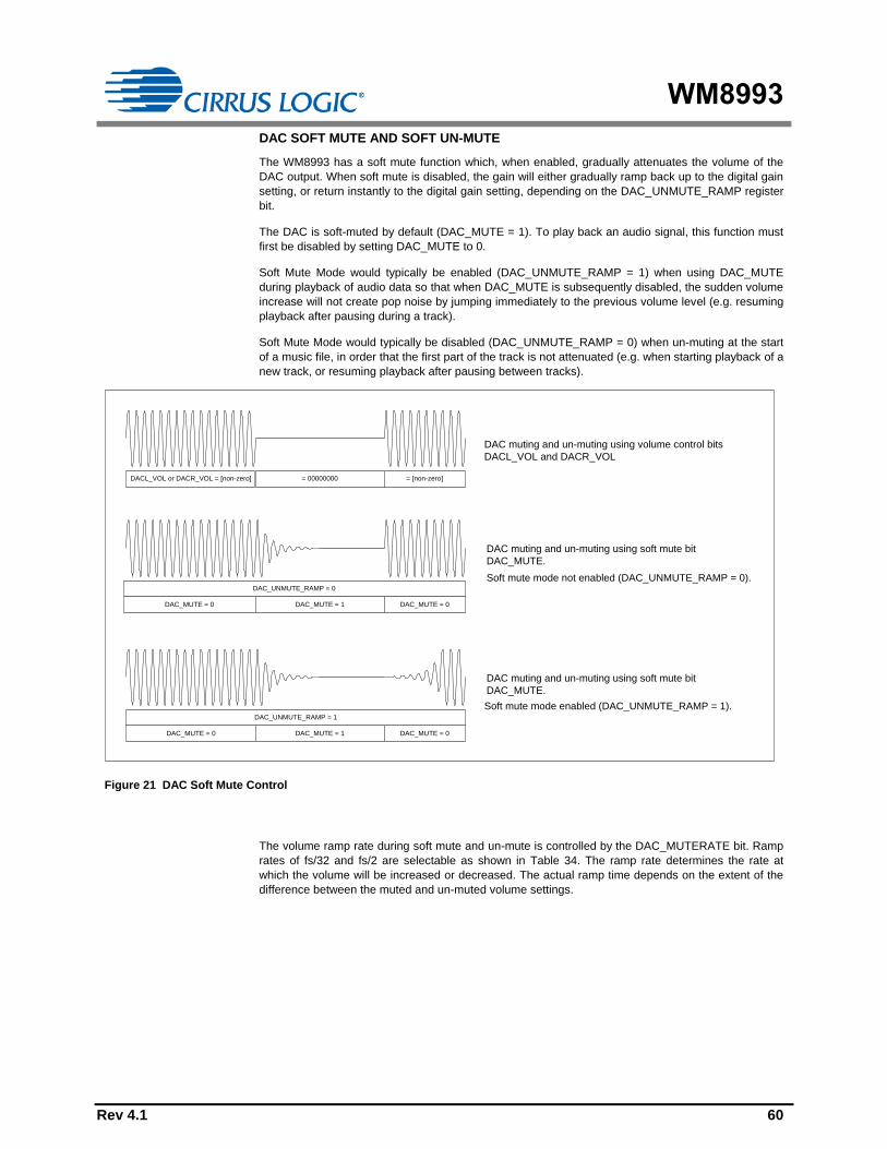
WM8993
Rev 4.1 60
DAC SOFT MUTE AND SOFT UN-MUTE
The WM8993 has a soft mute function which, when enabled, gradually attenuates the volume of the
DAC output. When soft mute is disabled, the gain will either gradually ramp back up to the digital gain
setting, or return instantly to the digital gain setting, depending on the DAC_UNMUTE_RAMP register
bit.
The DAC is soft-muted by default (DAC_MUTE = 1). To play back an audio signal, this function must
first be disabled by setting DAC_MUTE to 0.
Soft Mute Mode would typically be enabled (DAC_UNMUTE_RAMP = 1) when using DAC_MUTE
during playback of audio data so that when DAC_MUTE is subsequently disabled, the sudden volume
increase will not create pop noise by jumping immediately to the previous volume level (e.g. resuming
playback after pausing during a track).
Soft Mute Mode would typically be disabled (DAC_UNMUTE_RAMP = 0) when un-muting at the start
of a music file, in order that the first part of the track is not attenuated (e.g. when starting playback of a
new track, or resuming playback after pausing between tracks).
= 00000000 = [non-zero]
DAC_MUTE = 0 DAC_MUTE = 1 DAC_MUTE = 0
DAC_MUTE = 0 DAC_MUTE = 1 DAC_MUTE = 0
DACL_VOL or DACR_VOL = [non-zero]
DAC_UNMUTE_RAMP = 0
DAC_UNMUTE_RAMP = 1
DAC muting and un-muting using volume control bits
DACL_VOL and DACR_VOL
DAC muting and un-muting using soft mute bit
DAC_MUTE.
Soft mute mode not enabled (DAC_UNMUTE_RAMP = 0).
DAC muting and un-muting using soft mute bit
DAC_MUTE.
Soft mute mode enabled (DAC_UNMUTE_RAMP = 1).
Figure 21 DAC Soft Mute Control
The volume ramp rate during soft mute and un-mute is controlled by the DAC_MUTERATE bit. Ramp
rates of fs/32 and fs/2 are selectable as shown in Table 34. The ramp rate determines the rate at
which the volume will be increased or decreased. The actual ramp time depends on the extent of the
difference between the muted and un-muted volume settings.

WM8993
Rev 4.1 61
REGISTER
ADDRESS
BIT LABEL DEFAULT DESCRIPTION
R10 (0Ah)
DAC CTRL
7 DAC_MUTERATE 0 DAC Soft Mute Ramp Rate
0 = Fast ramp (fs/2, maximum ramp
time is 10.7ms at fs=48k)
1 = Slow ramp (fs/32, maximum
ramp time is 171ms at fs=48k)
(Note: ramp rate scales with sample
rate.)
6 DAC_UNMUTE_RAMP 0 DAC Unmute Ramp select
0 = Disabling soft-mute
(DAC_MUTE=0) will cause the DAC
volume to change immediately to
DACL_VOL and DACR_VOL
settings
1 = Disabling soft-mute
(DAC_MUTE=0) will cause the DAC
volume to ramp up gradually to the
DACL_VOL and DACR_VOL
settings
2 DAC_MUTE 1 DAC Soft Mute Control
0 = DAC Un-mute
1 = DAC Mute
Table 34 DAC Soft-Mute Control
DAC MONO MIX
A DAC digital mono-mix mode can be enabled using the DAC_MONO register bit. The mono mix is
generated as the sum of the Left and Right channel DAC data. To prevent clipping, a -6dB attenuation
is automatically applied to the mono mix.
The mono mix is only supported when one or other DAC is disabled. If DACL_ENA and DACR_ENA
are both set, then stereo operation applies.
REGISTER
ADDRESS
BIT LABEL DEFAULT DESCRIPTION
R10 (0Ah)
DAC CTRL
9 DAC_MONO 0 DAC Mono Mix
0 = Disabled
1 = Enabled
Only valid when one or other
DAC is disabled.
Table 35 DAC Mono Mix
DAC DE-EMPHASIS
Digital de-emphasis can be applied to the DAC playback data; this is appropriate when the data
source is a CD where pre-emphasis is used in the recording. De-emphasis filtering is available for
sample rates of 48kHz, 44.1kHz and 32kHz. See "Digital Filter Characteristics" section for details of
de-emphasis filter characteristics.
REGISTER
ADDRESS
BIT LABEL DEFAULT DESCRIPTION
R10 (0Ah)
DAC CTRL
5:4 DEEMPH
[1:0]
00 DAC De-Emphasis Control
00 = No de-emphasis
01 = 32kHz sample rate
10 = 44.1kHz sample rate
11 = 48kHz sample rate
Table 36 DAC De-Emphasis Control

WM8993
Rev 4.1 62
DAC SLOPING STOPBAND FILTER
Two DAC filter types are available, selected by the register bit DAC_SB_FILT. When operating at
lower sample rates (e.g. during voice communication) it is recommended that the sloping stopband
filter type is selected (DAC_SB_FILT=1) to reduce out-of-band noise which can be audible at low DAC
sample rates. See "Digital Filter Characteristics" section for details of DAC filter characteristics.
The DAC filter type is determined automatically by the WM8993 in Automatic Clocking Configuration
mode. The DAC_SB_FILT register bit is only effective in Manual Clocking Configuration mode. See
“Clocking and Sample Rates” for details of the Clocking Configuration mode selection.
REGISTER
ADDRESS
BIT LABEL DEFAULT DESCRIPTION
R10 (0Ah)
DAC CTRL
8 DAC_SB_FILT 0 Selects DAC filter characteristics
0 = Normal mode
1 = Sloping stopband mode
Note - this field is ignored and invalid
in Automatic Clocking Configuration
mode.
Table 37 DAC Sloping Stopband Filter
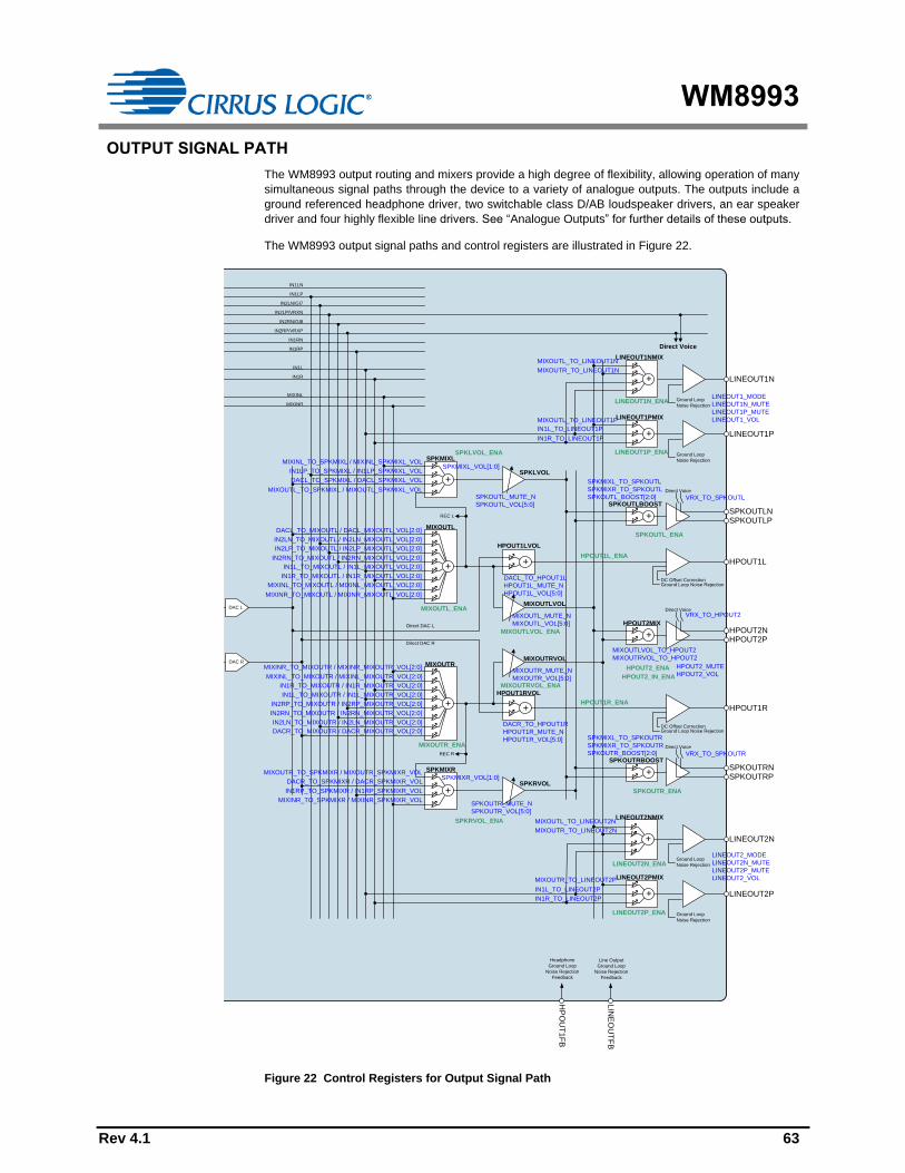
WM8993
Rev 4.1 63
OUTPUT SIGNAL PATH
The WM8993 output routing and mixers provide a high degree of flexibility, allowing operation of many
simultaneous signal paths through the device to a variety of analogue outputs. The outputs include a
ground referenced headphone driver, two switchable class D/AB loudspeaker drivers, an ear speaker
driver and four highly flexible line drivers. See “Analogue Outputs” for further details of these outputs.
The WM8993 output signal paths and control registers are illustrated in Figure 22.
LINEOUT1N
LINEOUT1P
HPOUT1L
HPOUT1R
HPOUT2N
IN1R
IN1L
MIXINR
MIXINL
REC L
REC R
HP
OU
T1
FB
DAC L
DAC R
Ground Loop Noise Rejection
HPOUT2P
DC Offset Correction
SPKOUTLPSPKOUTLN
+
+
+
+
Direct Voice
Direct Voice
SPKOUTRPSPKOUTRN
Direct Voice
Direct Voice
+
+
+
+
IN1LP
IN1LN
IN1RN
IN2LN/GI7
IN2RN/GI8
IN1RP
IN2LP/VRXN
IN2RP/VRXP
SPKMIXL
SPKMIXR
MIXOUTL
MIXOUTR
LINEOUT1NMIX
LINEOUT1PMIX
HPOUT2MIX
Headphone
Ground Loop
Noise Rejection
Feedback
SPKOUTLBOOST
SPKOUTRBOOST
Ground Loop Noise RejectionDC Offset Correction
MIXOUTLVOL
HPOUT1LVOL
SPKLVOL
MIXOUTRVOL
HPOUT1RVOL
SPKRVOL
Direct DAC L
Direct DAC R
+
+
LINEOUT2N
LINEOUT2P+
LINEOUT2NMIX
LINEOUT2PMIX
LIN
EO
UT
FB
Line Output
Ground Loop
Noise Rejection
Feedback
+
+
HPOUT1R_ENA
LINEOUT2P_ENA
DACL_TO_HPOUT1L
HPOUT1L_MUTE_N
HPOUT1L_VOL[5:0]
LINEOUT2_MODE
LINEOUT2N_MUTE
LINEOUT2P_MUTE
LINEOUT2_VOL
HPOUT2_MUTE
HPOUT2_VOL
MIXOUTL_MUTE_N
MIXOUTL_VOL[5:0]
SPKMIXL_TO_SPKOUTR
SPKMIXR_TO_SPKOUTR
SPKOUTR_BOOST[2:0]
SPKOUTL_MUTE_N
SPKOUTL_VOL[5:0]
DACR_TO_MIXOUTR / DACR_MIXOUTR_VOL[2:0]
VRX_TO_HPOUT2
MIXOUTR_TO_LINEOUT2P
MIXINR_TO_SPKMIXR / MIXINR_SPKMIXR_VOL
Ground Loop
Noise Rejection
Ground Loop
Noise Rejection
Ground Loop
Noise Rejection
Ground Loop
Noise Rejection
MIXINR_TO_MIXOUTL / MIXINR_MIXOUTL_VOL[2:0]
SPKMIXL_VOL[1:0]
SPKMIXR_VOL[1:0]
DACR_TO_HPOUT1R
HPOUT1R_MUTE_N
HPOUT1R_VOL[5:0]
MIXOUTR_MUTE_N
MIXOUTR_VOL[5:0]
MIXOUTLVOL_TO_HPOUT2
MIXOUTRVOL_TO_HPOUT2
VRX_TO_SPKOUTR
VRX_TO_SPKOUTL
SPKMIXL_TO_SPKOUTL
SPKMIXR_TO_SPKOUTL
SPKOUTL_BOOST[2:0]
SPKOUTR_MUTE_N
SPKOUTR_VOL[5:0]
LINEOUT1_MODE
LINEOUT1N_MUTE
LINEOUT1P_MUTE
LINEOUT1_VOL
MIXOUTL_TO_LINEOUT2N
MIXOUTR_TO_LINEOUT2N
IN1R_TO_LINEOUT2P
IN1L_TO_LINEOUT2P
MIXOUTL_TO_LINEOUT1N
MIXOUTR_TO_LINEOUT1N
IN1R_TO_LINEOUT1P
IN1L_TO_LINEOUT1P
MIXOUTL_TO_LINEOUT1P
SPKOUTL_ENA
MIXOUTR_ENA
MIXINL_TO_SPKMIXL / MIXINL_SPKMIXL_VOL
IN1LP_TO_SPKMIXL / IN1LP_SPKMIXL_VOL
DACL_TO_SPKMIXL / DACL_SPKMIXL_VOL
MIXOUTL_TO_SPKMIXL / MIXOUTL_SPKMIXL_VOL
DACL_TO_MIXOUTL / DACL_MIXOUTL_VOL[2:0]
IN2LN_TO_MIXOUTL / IN2LN_MIXOUTL_VOL[2:0]
IN2LP_TO_MIXOUTL / IN2LP_MIXOUTL_VOL[2:0]
IN2RN_TO_MIXOUTL / IN2RN_MIXOUTL_VOL[2:0]
IN1L_TO_MIXOUTL / IN1L_MIXOUTL_VOL[2:0]
IN1R_TO_MIXOUTL / IN1R_MIXOUTL_VOL[2:0]
MIXINL_TO_MIXOUTL / MIXINL_MIXOUTL_VOL[2:0]
MIXINR_TO_MIXOUTR / MIXINR_MIXOUTR_VOL[2:0]
MIXINL_TO_MIXOUTR / MIXINL_MIXOUTR_VOL[2:0]
IN1R_TO_MIXOUTR / IN1R_MIXOUTR_VOL[2:0]
IN1L_TO_MIXOUTR / IN1L_MIXOUTR_VOL[2:0]
IN2RP_TO_MIXOUTR / IN2RP_MIXOUTR_VOL[2:0]
IN2RN_TO_MIXOUTR / IN2RN_MIXOUTR_VOL[2:0]
IN2LN_TO_MIXOUTR / IN2LN_MIXOUTR_VOL[2:0]
MIXOUTR_TO_SPKMIXR / MIXOUTR_SPKMIXR_VOL
DACR_TO_SPKMIXR / DACR_SPKMIXR_VOL
IN1RP_TO_SPKMIXR / IN1RP_SPKMIXR_VOL
SPKRVOL_ENA
SPKLVOL_ENA
SPKOUTR_ENA
MIXOUTLVOL_ENA
MIXOUTRVOL_ENA
MIXOUTL_ENA
HPOUT2_ENA
HPOUT1L_ENA
LINEOUT1N_ENA
LINEOUT1P_ENA
LINEOUT2N_ENA
HPOUT2_IN_ENA
Figure 22 Control Registers for Output Signal Path

WM8993
Rev 4.1 64
OUTPUT SIGNAL PATHS ENABLE
The output mixers and drivers can be independently enabled and disabled as described in Table 38.
Note that the headphone outputs HPOUT1L and HPOUT1R have dedicated output PGAs and volume
controls. As a result, a low power consumption DAC playback path can be supported without needing
to enable the output mixers MIXOUTL / MIXOUTR or the mixer output PGAs MIXOUTLVOL /
MIXOUTRVOL.
REGISTER
ADDRESS
BIT LABEL DEFAULT DESCRIPTION
R1 (01h)
Power
Management
(1)
13 SPKOUTR_ENA 0b SPKMIXR Mixer, SPKRVOL PGA
and SPKOUTR Output Enable
0 = Disabled
1 = Enabled
12 SPKOUTL_ENA 0b SPKMIXL Mixer, SPKLVOL PGA
and SPKOUTL Output Enable
0 = Disabled
1 = Enabled
11 HPOUT2_ENA 0b HPOUT2 Output Stage Enable
0 = Disabled
1 = Enabled
9 HPOUT1L_ENA 0b Enables HPOUT1L input stage
0 = Disabled
1 = Enabled
Note: When HPOUT1_AUTO_PU is
set, the HPOUT1L_ENA bit
automatically enables all stages of
the left headphone driver
8 HPOUT1R_ENA 0b Enables HPOUT1R input stage
0 = Disabled
1 = Enabled
Note: When HPOUT1_AUTO_PU is
set, the HPOUT1R_ENA bit
automatically enables all stages of
the right headphone driver
R3 (03h)
Power
Management
(3)
13 LINEOUT1N_ENA 0b LINEOUT1N Line Out and
LINEOUT1NMIX Enable
0 = Disabled
1 = Enabled
12 LINEOUT1P_ENA 0b LINEOUT1P Line Out and
LINEOUT1PMIX Enable
0 = Disabled
1 = Enabled
11 LINEOUT2N_ENA 0b LINEOUT2N Line Out and
LINEOUT2NMIX Enable
0 = Disabled
1 = Enabled
10 LINEOUT2P_ENA 0b LINEOUT2P Line Out and
LINEOUT2PMIX Enable
0 = Disabled
1 = Enabled
9 SPKRVOL_ENA 0b SPKMIXR Mixer and SPKRVOL
PGA Enable
0 = Disabled
1 = Enabled
Note that SPKMIXR and SPKRVOL
are also enabled when
SPKOUTR_ENA is set.

WM8993
Rev 4.1 65
REGISTER
ADDRESS
BIT LABEL DEFAULT DESCRIPTION
8 SPKLVOL_ENA 0b SPKMIXL Mixer and SPKLVOL
PGA Enable
0 = Disabled
1 = Enabled
Note that SPKMIXL and SPKLVOL
are also enabled when
SPKOUTL_ENA is set.
7 MIXOUTLVOL_ENA 0b MIXOUTL Left Volume Control
Enable
0 = Disabled
1 = Enabled
6 MIXOUTRVOL_ENA 0b MIXOUTR Right Volume Control
Enable
0 = Disabled
1 = Enabled
5 MIXOUTL_ENA 0b MIXOUTL Left Output Mixer Enable
0 = Disabled
1 = Enabled
4 MIXOUTR_ENA 0b MIXOUTR Right Output Mixer
Enable
0 = Disabled
1 = Enabled
R56 (38h)
AntiPOP1
6 HPOUT2_IN_ENA 0b HPOUT2MIX Mixer and Input Stage
Enable
0 = Disabled
1 = Enabled
Table 38 Output Signal Paths Enable
HEADPHONE SIGNAL PATHS ENABLE
The HPOUT1L and HPOUT1R output paths can be actively discharged to AGND through internal
resistors if desired. This is desirable at start-up in order to achieve a known output stage condition
prior to enabling the VMID reference voltage. This is also desirable in shutdown to prevent the
external connections from being affected by the internal circuits. The HPOUT1L and HPOUT1R
outputs are shorted to AGND by default; the short circuit is removed on each of these paths by setting
the applicable fields HPOUT1L_RMV_SHORT or HPOUT1R_RMV_SHORT.
The ground-referenced Headphone output drivers are designed to suppress pops and clicks when
enabled or disabled. However, it is necessary to control the drivers in accordance with a defined
sequence in start-up and shut-down to achieve the pop suppression. It is also necessary to schedule
the DC Servo offset correction at the appropriate point in the sequence (see “DC Servo”). Table 39
and Table 40 describe the recommended sequences for enabling and disabling these output drivers.
SEQUENCE HEADPHONE ENABLE
Step 1 HPOUT1L_ENA = 1
HPOUT1R_ENA = 1
Step 2 20s delay
Step 3 HPOUT1L_DLY = 1
HPOUT1R_DLY = 1
Step 4 DC offset correction
Step 5 HPOUT1L_OUTP = 1
HPOUT1L_RMV_SHORT = 1
HPOUT1R_OUTP = 1
HPOUT1R_RMV_SHORT = 1
Table 39 Headphone Output Enable Sequence

WM8993
Rev 4.1 66
SEQUENCE HEADPHONE DISABLE
Step 1 HPOUT1L_RMV_SHORT = 0
HPOUT1L_DLY = 0
HPOUT1L_OUTP = 0
HPOUT1R_RMV_SHORT = 0
HPOUT1R_DLY = 0
HPOUT1R_OUTP = 0
Step 2 HPOUT1L_ENA = 0
HPOUT1R_ENA = 0
Table 40 Headphone Output Disable Sequence
The sequences described above in Table 39 and Table 40 are implemented automatically by the
WM8993 when the HPOUT1_AUTO_PU bit is set, which is the default condition. In this mode, the
enable sequence is triggered by setting the HPOUT1L_ENA and HPOUT1R_ENA bits in register R1.
Note that the Charge Pump is also enabled automatically in this mode.
The register bits relating to pop suppression control are defined in Table 41.
REGISTER
ADDRESS
BIT LABEL DEFAULT DESCRIPTION
R1 (01h)
Power
Management
(1)
9 HPOUT1L_ENA 0b Enables HPOUT1L input stage
0 = Disabled
1 = Enabled
For normal operation, this bit should
be set as the first step of the
HPOUT1L Enable sequence.
Note: When HPOUT1_AUTO_PU is
set, the HPOUT1L_ENA bit
automatically enables all stages of the
left headphone driver
8 HPOUT1R_ENA 0b Enables HPOUT1R input stage
0 = Disabled
1 = Enabled
For normal operation, this bit should
be set as the first step of the
HPOUT1R Enable sequence.
Note: When HPOUT1_AUTO_PU is
set, the HPOUT1R_ENA bit
automatically enables all stages of the
right headphone driver
R96 (60h)
Analogue HP
0
8 HPOUT1_AUTO_
PU
1b Enables automatic power-up of
HPOUT1 by monitoring
HPOUT1L_ENA and HPOUT1R_ENA
0 = Disabled
1 = Enabled
7 HPOUT1L_RMV_
SHORT
0b Removes HPOUT1L short
0 = HPOUT1L short enabled
1 = HPOUT1L short removed
For normal operation, this bit should
be set as the final step of the
HPOUT1L Enable sequence.
6 HPOUT1L_OUTP 0b Enables HPOUT1L output stage
0 = Disabled
1 = Enabled
For normal operation, this bit should
be set to 1 after the DC offset
cancellation has been scheduled.

WM8993
Rev 4.1 67
REGISTER
ADDRESS
BIT LABEL DEFAULT DESCRIPTION
5 HPOUT1L_DLY 0b Enables HPOUT1L intermediate stage
0 = Disabled
1 = Enabled
For normal operation, this bit should
be set to 1 after the output signal path
has been configured, and before DC
offset cancellation is scheduled. This
bit should be set with at least 20us
delay after HPOUT1L_ENA.
3 HPOUT1R_RMV_
SHORT
0b Removes HPOUT1R short
0 = HPOUT1R short enabled
1 = HPOUT1R short removed
For normal operation, this bit should
be set as the final step of the
HPOUT1R Enable sequence.
2 HPOUT1R_OUTP 0b Enables HPOUT1R output stage
0 = Disabled
1 = Enabled
For normal operation, this bit should
be set to 1 after the DC offset
cancellation has been scheduled.
1 HPOUT1R_DLY 0b Enables HPOUT1R intermediate stage
0 = Disabled
1 = Enabled
For normal operation, this bit should
be set to 1 after the output signal path
has been configured, and before DC
offset cancellation is scheduled. This
bit should be set with at least 20us
delay after HPOUT1R_ENA.
Table 41 Pop Suppression Control
OUTPUT MIXER CONTROL
The Output Mixer path select and volume controls are described in Table 42 for the Left Channel
(MIXOUTL) and Table 43 for the Right Channel (MIXOUTR). The gain of each of input path may be
controlled independently in the range described in Table 44. The DAC input levels may also be
controlled by the DAC digital volume control - see “Digital to Analogue Converter (DAC)” for further
details.
REGISTER
ADDRESS
BIT LABEL DEFAULT DESCRIPTION
R45 (2Dh)
Output Mixer1
5 IN2RN_TO_MIXOUTL 0b IN2RN to MIXOUTL Mute
0 = Mute
1 = Un-mute
R49 (31h)
Output Mixer5
8:6 IN2RN_MIXOUTL_VOL
[2:0]
000b IN2RN to MIXOUTL Volume
0dB to -21dB in 3dB steps
(See Table 44 for Volume Range)
R45 (2Dh)
Output Mixer1
4 IN2LN_TO_MIXOUTL 0b IN2LN to MIXOUTL Mute
0 = Mute
1 = Un-mute
R47 (2Fh)
Output Mixer3
8:6 IN2LN_MIXOUTL_VOL
[2:0]
000b IN2LN to MIXOUTL Volume
0dB to -21dB in 3dB steps
(See Table 44 for Volume Range)

WM8993
Rev 4.1 68
REGISTER
ADDRESS
BIT LABEL DEFAULT DESCRIPTION
R45 (2Dh)
Output Mixer1
2 IN1L_TO_MIXOUTL 0b IN1L PGA Output to MIXOUTL
Mute
0 = Mute
1 = Un-mute
R47 (2Fh)
Output Mixer3
2:0 IN1L_MIXOUTL_VOL
[2:0]
000b IN1L PGA Output to MIXOUTL
Volume
0dB to -21dB in 3dB steps
(See Table 44 for Volume Range)
R45 (2Dh)
Output Mixer1
3 IN1R_TO_MIXOUTL 0 IN1R PGA Output to MIXOUTL
Mute
0 = Mute
1 = Un-mute
R47 (2Fh)
Output Mixer3
5:3 IN1R_MIXOUTL_VOL
[2:0]
000b IN1R PGA Output to MIXOUTL
Volume
0dB to -21dB in 3dB steps
(See Table 44 for Volume Range)
R45 (2Dh)
Output Mixer1
1 IN2LP_TO_MIXOUTL 0b IN2LP to MIXOUTL Mute
0 = Mute
1 = Un-mute
R47 (2Fh)
Output Mixer3
11:9 IN2LP_MIXOUTL_VOL
[2:0]
000b IN2LP to MIXOUTL Volume
0dB to -21dB in 3dB steps
(See Table 44 for Volume Range)
R45 (2Dh)
Output Mixer1
7 MIXINR_TO_MIXOUTL 0b MIXINR Output (Right ADC bypass)
to MIXOUTL Mute
0 = Mute
1 = Un-mute
R49 (31h)
Output Mixer5
5:3 MIXINR_MIXOUTL_VO
L [2:0]
000b MIXINR Output (Right ADC bypass)
to MIXOUTL Volume
0dB to -21dB in 3dB steps
(See Table 44 for Volume Range)
R45 (2Dh)
Output Mixer1
6 MIXINL_TO_MIXOUTL 0b MIXINL Output (Left ADC bypass)
to MIXOUTL Mute
0 = Mute
1 = Un-mute
R49 (31h)
Output Mixer5
2:0 MIXINL_MIXOUTL_VOL
[2:0]
000b MIXINL Output (Left ADC bypass)
to MIXOUTL Volume
0dB to -21dB in 3dB steps
(See Table 44 for Volume Range)
R45 (2Dh)
Output Mixer1
0 DACL_TO_MIXOUTL 0b Left DAC to MIXOUTL Mute
0 = Mute
1 = Un-mute
R49 (31h)
Output Mixer5
11:9 DACL_MIXOUTL_VOL
[2:0]
000b Left DAC to MIXOUTL Volume
0dB to -21dB in 3dB steps
(See Table 44 for Volume Range)
Table 42 Left Output Mixer (MIXOUTL) Control

WM8993
Rev 4.1 69
REGISTER
ADDRESS
BIT LABEL DEFAULT DESCRIPTION
R46 (2Eh)
Output Mixer2
5 IN2LN_TO_MIXOUTR 0b IN2LN to MIXOUTR Mute
0 = Mute
1 = Un-mute
R50 (32h)
Output Mixer6
8:6 IN2LN_MIXOUTR_VOL
[2:0]
000b IN2LN to MIXOUTR Volume
0dB to -21dB in 3dB steps
(See Table 44 for Volume Range)
R46 (2Eh)
Output Mixer2
4 IN2RN_TO_MIXOUTR 0b IN2RN to MIXOUTR Mute
0 = Mute
1 = Un-mute
R48 (30h)
Output Mixer4
8:6 IN2RN_MIXOUTR_VOL
[2:0]
000b IN2RN to MIXOUTR Volume
0dB to -21dB in 3dB steps
(See Table 44 for Volume Range)
R46 (2Eh)
Output Mixer2
3 IN1L_TO_MIXOUTR 0b IN1L PGA Output to MIXOUTR Mute
0 = Mute
1 = Un-mute
R48 (30h)
Output Mixer4
5:3 IN1L_MIXOUTR_VOL
[2:0]
000b IN1L PGA Output to MIXOUTR
Volume
0dB to -21dB in 3dB steps
(See Table 44 for Volume Range)
R46 (2Eh)
Output Mixer2
2 IN1R_TO_MIXOUTR 0 IN1R PGA Output to MIXOUTR
Mute
0 = Mute
1 = Un-mute
R48 (30h)
Output Mixer4
2:0 IN1R_MIXOUTR_VOL
[2:0]
000b IN1R PGA Output to MIXOUTR
Volume
0dB to -21dB in 3dB steps
(See Table 44 for Volume Range)
R46 (2Eh)
Output Mixer2
1 IN2RP_TO_MIXOUTR 0b IN2RP to MIXOUTR Mute
0 = Mute
1 = Un-mute
R48 (30h)
Output Mixer4
11:9 IN2RP_MIXOUTR_VOL
[2:0]
000b IN2RP to MIXOUTR Volume
0dB to -21dB in 3dB steps
(See Table 44 for Volume Range)
R46 (2Eh)
Output Mixer2
7 MIXINL_TO_MIXOUTR 0b MIXINL Output (Left ADC bypass) to
MIXOUTR Mute
0 = Mute
1 = Un-mute
R50 (32h)
Output Mixer6
5:3 MIXINL_MIXOUTR_VO
L[2:0]
000b MIXINL Output (Left ADC bypass) to
MIXOUTR Volume
0dB to -21dB in 3dB steps
(See Table 44 for Volume Range)
R46 (2Eh)
Output Mixer2
6 MIXINR_TO_MIXOUTR 0b MIXINR Output (Right ADC bypass)
to MIXOUTR Mute
0 = Mute
1 = Un-mute
R50 (32h)
Output Mixer6
2:0 MIXINR_MIXOUTR_VO
L [2:0]
000b MIXINR Output (Right ADC bypass)
to MIXOUTR Volume
0dB to -21dB in 3dB steps
(See Table 44 for Volume Range)
R46 (2Eh)
Output Mixer2
0 DACR_TO_MIXOUTR 0b Right DAC to MIXOUTR Mute
0 = Mute
1 = Un-mute
R50 (32h)
Output Mixer6
11:9 DACR_MIXOUTR_VOL
[2:0]
000b Right DAC to MIXOUTR Volume
0dB to -21dB in 3dB steps
(See Table 44 for Volume Range)
Table 43 Right Output Mixer (MIXOUTR) Control

WM8993
Rev 4.1 70
VOLUME SETTING VOLUME
(dB)
000 0
001 -3
010 -6
011 -9
100 -12
101 -15
110 -18
111 -21
Table 44 MIXOUTL and MIXOUTR Volume Range
SPEAKER MIXER CONTROL
The Speaker Mixer path select and volume controls are described in Table 45 for the Left Channel
(SPKMIXL) and Table 46 for the Right Channel (SPKMIXR).
Care should be taken when enabling more than one path to a speaker mixer in order to avoid clipping.
The gain of each input path is adjustable using a selectable -3dB control in each path to facilitate this.
Each Speaker Mixer output is also controlled by an additional independent volume control. The DAC
input levels may also be controlled by the DAC digital volume control - see “Digital to Analogue
Converter (DAC)” for further details.
REGISTER
ADDRESS
BIT LABEL DEFAULT DESCRIPTION
R54 (36h)
Speaker Mixer
7 MIXINL_TO_SPKMIXL 0b MIXINL (Left ADC bypass) to
SPKMIXL Mute
0 = Mute
1 = Un-mute
5 IN1LP_TO_SPKMIXL 0b IN1LP to SPKMIXL Mute
0 = Mute
1 = Un-mute
3 MIXOUTL_TO_SPKMIX
L
0b Left Mixer Output to SPKMIXL
Mute
0 = Mute
1 = Un-mute
1 DACL_TO_SPKMIXL 0b Left DAC to SPKMIXL Mute
0 = Mute
1 = Un-mute
R34 (22h)
SPKMIXL
Attenuation
5 MIXINL_SPKMIXL_VOL 0b MIXINL (Left ADC bypass) to
SPKMIXL Fine Volume Control
0 = 0dB
1 = -3dB
4 IN1LP_SPKMIXL_VOL 0b IN1LP to SPKMIXL Fine Volume
Control
0 = 0dB
1 = -3dB
3 MIXOUTL_SPKMIXL_V
OL
0b Left Mixer Output to SPKMIXL Fine
Volume Control
0 = 0dB
1 = -3dB
2 DACL_SPKMIXL_VOL 0b Left DAC to SPKMIXL Fine Volume
Control
0 = 0dB
1 = -3dB

WM8993
Rev 4.1 71
REGISTER
ADDRESS
BIT LABEL DEFAULT DESCRIPTION
1:0 SPKMIXL_VOL [1:0] 11b Left Speaker Mixer Volume Control
00 = 0dB
01 = -6dB
10 = -12dB
11 = mute
Table 45 Left Speaker Mixer (SPKMIXL) Control
REGISTER
ADDRESS
BIT LABEL DEFAULT DESCRIPTION
R54 (36h)
Speaker
Mixer
6 MIXINR_TO_SPKMIXR 0b MIXINR (Right ADC bypass) to
SPKMIXR Mute
0 = Mute
1 = Un-mute
4 IN1RP_TO_SPKMIXR 0b IN1RP to SPKMIXR Mute
0 = Mute
1 = Un-mute
2 MIXOUTR_TO_SPKMIX
R
0b Right Mixer Output to SPKMIXR
Mute
0 = Mute
1 = Un-mute
0 DACR_TO_SPKMIXR 0b Right DAC to SPKMIXR Mute
0 = Mute
1 = Un-mute
R35 (22h)
SPKMIXR
Attenuation
5 MIXINR_SPKMIXR_VOL 0b MIXINR (Right ADC bypass) to
SPKMIXR Fine Volume Control
0 = 0dB
1 = -3dB
4 IN1RP_SPKMIXR_VOL 0b IN1RP to SPKMIXR Fine Volume
Control
0 = 0dB
1 = -3dB
3 MIXOUTR_SPKMIXR_V
OL
0b Right Mixer Output to SPKMIXR
Fine Volume Control
0 = 0dB
1 = -3dB
2 DACR_SPKMIXR_VOL 0b Right DAC to SPKMIXR Fine
Volume Control
0 = 0dB
1 = -3dB
1:0 SPKMIXR_VOL [1:0] 11b Right Speaker Mixer Volume
Control
00 = 0dB
01 = -6dB
10 = -12dB
11 = mute
Table 46 Right Speaker Mixer (SPKMIXR) Control
OUTPUT SIGNAL PATH VOLUME CONTROL
There are six output PGAs - MIXOUTLVOL, MIXOUTRVOL, HPOUT1LVOL, HPOUT1RVOL,
SPKLVOL and SPKRVOL. Each can be independently controlled, with MIXOUTLVOL and
MIXOUTRVOL providing volume control to both the earpiece and line drivers, HPOUT1LVOL and
HPOUT1RVOL to the headphone driver, and SPKLVOL and SPKRVOL to the speaker drivers.
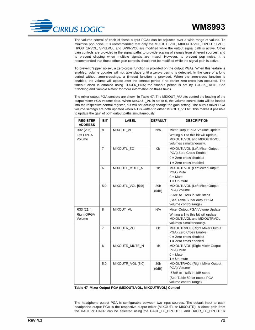
WM8993
Rev 4.1 72
The volume control of each of these output PGAs can be adjusted over a wide range of values. To
minimise pop noise, it is recommended that only the MIXOUTLVOL, MIXOUTRVOL, HPOUT1LVOL,
HPOUT1RVOL, SPKLVOL and SPKRVOL are modified while the output signal path is active. Other
gain controls are provided in the signal paths to provide scaling of signals from different sources, and
to prevent clipping when multiple signals are mixed. However, to prevent pop noise, it is
recommended that those other gain controls should not be modified while the signal path is active.
To prevent "zipper noise", a zero-cross function is provided on the output PGAs. When this feature is
enabled, volume updates will not take place until a zero-crossing is detected. In the case of a long
period without zero-crossings, a timeout function is provided. When the zero-cross function is
enabled, the volume will update after the timeout period if no earlier zero-cross has occurred. The
timeout clock is enabled using TOCLK_ENA; the timeout period is set by TOCLK_RATE. See
“Clocking and Sample Rates” for more information on these fields.
The mixer output PGA controls are shown in Table 47. The MIXOUT_VU bits control the loading of the
output mixer PGA volume data. When MIXOUT_VU is set to 0, the volume control data will be loaded
into the respective control register, but will not actually change the gain setting. The output mixer PGA
volume settings are both updated when a 1 is written to either MIXOUT_VU bit. This makes it possible
to update the gain of both output paths simultaneously.
REGISTER
ADDRESS
BIT LABEL DEFAULT DESCRIPTION
R32 (20h)
Left OPGA
Volume
8 MIXOUT_VU N/A Mixer Output PGA Volume Update
Writing a 1 to this bit will update
MIXOUTLVOL and MIXOUTRVOL
volumes simultaneously.
7 MIXOUTL_ZC 0b MIXOUTLVOL (Left Mixer Output
PGA) Zero Cross Enable
0 = Zero cross disabled
1 = Zero cross enabled
6 MIXOUTL_MUTE_N 1b MIXOUTLVOL (Left Mixer Output
PGA) Mute
0 = Mute
1 = Un-mute
5:0 MIXOUTL_VOL [5:0] 39h
(0dB)
MIXOUTLVOL (Left Mixer Output
PGA) Volume
-57dB to +6dB in 1dB steps
(See Table 50 for output PGA
volume control range)
R33 (21h)
Right OPGA
Volume
8 MIXOUT_VU N/A Mixer Output PGA Volume Update
Writing a 1 to this bit will update
MIXOUTLVOL and MIXOUTRVOL
volumes simultaneously.
7 MIXOUTR_ZC 0b MIXOUTRVOL (Right Mixer Output
PGA) Zero Cross Enable
0 = Zero cross disabled
1 = Zero cross enabled
6 MIXOUTR_MUTE_N 1b MIXOUTLVOL (Right Mixer Output
PGA) Mute
0 = Mute
1 = Un-mute
5:0 MIXOUTR_VOL [5:0] 39h
(0dB)
MIXOUTRVOL (Right Mixer Output
PGA) Volume
-57dB to +6dB in 1dB steps
(See Table 50 for output PGA
volume control range)
Table 47 Mixer Output PGA (MIXOUTLVOL, MIXOUTRVOL) Control
The headphone output PGA is configurable between two input sources. The default input to each
headphone output PGA is the respective output mixer (MIXOUTL or MIXOUTR). A direct path from
the DACL or DACR can be selected using the DACL_TO_HPOUT1L and DACR_TO_HPOUT1R

WM8993
Rev 4.1 73
register bits. When these bits are selected, a DAC to Headphone playback path is possible without
using the output mixers; this offers reduced power consumption by allowing the output mixers to be
disabled in this typical usage case.
The headphone output PGA controls are shown in Table 48. The HPOUT1_VU bits control the loading
of the headphone PGA volume data. When HPOUT1_VU is set to 0, the volume control data will be
loaded into the respective control register, but will not actually change the gain setting. The
headphone PGA volume settings are both updated when a 1 is written to either HPOUT1_VU bit. This
makes it possible to update the gain of both output paths simultaneously.
REGISTER
ADDRESS
BIT LABEL DEFAULT DESCRIPTION
R28 (1Ch)
Left Output
Volume
8 HPOUT1_VU N/A Headphone Output PGA Volume
Update
Writing a 1 to this bit will update
HPOUT1LVOL and HPOUT1RVOL
volumes simultaneously.
7 HPOUT1L_ZC 0b HPOUT1LVOL (Left Headphone
Output PGA) Zero Cross Enable
0 = Zero cross disabled
1 = Zero cross enabled
6 HPOUT1L_MUTE_N 1b HPOUT1LVOL (Left Headphone
Output PGA) Mute
0 = Mute
1 = Un-mute
5:0 HPOUT1L_VOL [5:0] 2Dh
(-12dB)
HPOUT1LVOL (Left Headphone
Output PGA) Volume
-57dB to +6dB in 1dB steps
(See Table 50 for output PGA
volume control range)
R45 (2Dh)
Output
Mixer1
8 DACL_TO_HPOUT1L 0b HPOUT1LVOL (Left Headphone
Output PGA) Input Select
0 = MIXOUTL
1 = DACL
R29 (1Dh)
Right Output
Volume
8 HPOUT1_VU N/A Headphone Output PGA Volume
Update
Writing a 1 to this bit will update
HPOUT1LVOL and HPOUT1RVOL
volumes simultaneously.
7 HPOUT1R_ZC 0b HPOUT1RVOL (Right Headphone
Output PGA) Zero Cross Enable
0 = Zero cross disabled
1 = Zero cross enabled
6 HPOUT1R_MUTE_N 1b HPOUT1RVOL (Right Headphone
Output PGA) Mute
0 = Mute
1 = Un-mute
5:0 HPOUT1R_VOL [5:0] 2Dh
(-12dB)
HPOUT1RVOL (Right Headphone
Output PGA) Volume
-57dB to +6dB in 1dB steps
(See Table 50 for output PGA
volume control range)
R46 (2Eh)
Output
Mixer2
8 DACR_TO_HPOUT1
R
0b HPOUT1RVOL (Right Headphone
Output PGA) Input Select
0 = MIXOUTR
1 = DACR
Table 48 Headphone Output PGA (HPOUT1LVOL, HPOUT1RVOL) Control

WM8993
Rev 4.1 74
The speaker output PGA controls are shown in Table 49.The SPKOUT_VU bits control the loading of
the speaker PGA volume data. When SPKOUT_VU is set to 0, the volume control data will be loaded
into the respective control register, but will not actually change the gain setting. The speaker PGA
volume settings are both updated when a 1 is written to either SPKOUT_VU bit. This makes it
possible to update the gain of both output paths simultaneously.
REGISTER
ADDRESS
BIT LABEL DEFAULT DESCRIPTION
R38 (26h)
Speaker
Volume Left
8 SPKOUT_VU N/A Speaker Output PGA Volume
Update
Writing a 1 to this bit will update
SPKLVOL and SPKRVOL volumes
simultaneously.
7 SPKOUTL_ZC 0b SPKLVOL (Left Speaker Output
PGA) Zero Cross Enable
0 = Zero cross disabled
1 = Zero cross enabled
6 SPKOUTL_MUTE_N 1b SPKLVOL (Left Speaker Output
PGA) Mute
0 = Mute
1 = Un-mute
5:0 SPKOUTL_VOL [5:0] 39h
(0dB)
SPKLVOL (Left Speaker Output
PGA) Volume
-57dB to +6dB in 1dB steps
(See Table 50 for output PGA
volume control range)
R39 (27h)
Speaker
Volume Right
8 SPKOUT_VU N/A Speaker PGA Volume Update
Writing a 1 to this bit will update
SPKLVOL and SPKRVOL volumes
simultaneously.
7 SPKOUTR_ZC 0b SPKRVOL (Right Speaker Output
PGA) Zero Cross Enable
0 = Zero cross disabled
1 = Zero cross enabled
6 SPKOUTR_MUTE_N 1b SPKRVOL (Right Speaker Output
PGA) Mute
0 = Mute
1 = Un-mute
5:0 SPKOUTR_VOL [5:0] 39h
(0dB)
SPKRVOL (Right Speaker Output
PGA) Volume
-57dB to +6dB in 1dB steps
(See Table 50 for output PGA
volume control range)
Table 49 Speaker Output PGA (SPKLVOL, SPKRVOL) Control

WM8993
Rev 4.1 75
PGA GAIN SETTING VOLUME (dB) PGA GAIN SETTING VOLUME (dB)
0h -57 20h -25
1h -56 21h -24
2h -55 22h -23
3h -54 23h -22
4h -53 24h -21
5h -52 25h -20
6h -51 26h -19
7h -50 27h -18
8h -49 28h -17
9h -48 29h -16
Ah -47 2Ah -15
Bh -46 2Bh -14
Ch -45 2Ch -13
Dh -44 2Dh -12
Eh -43 2Eh -11
Fh -42 2Fh -10
10h -41 30h -9
11h -40 31h -8
12h -39 32h -7
13h -38 33h -6
14h -37 34h -5
15h -36 35h -4
16h -35 36h -3
17h -34 37h -2
18h -33 38h -1
19h -32 39h 0
1Ah -31 3Ah +1
1Bh -30 3Bh +2
1Ch -29 3Ch +3
1Dh -28 3Dh +4
1Eh -27 3Eh +5
1Fh -26 3Fh +6
Table 50 Output PGA Volume Range

WM8993
Rev 4.1 76
SPEAKER BOOST MIXER
Each class D/AB speaker driver has its own boost mixer which performs a dual role. It allows the
output from the left speaker mixer (via SPKLVOL), right speaker mixer (via SPKRVOL), or the ‘Direct
Voice’ path to be routed to either speaker driver. (The ‘Direct Voice’ path is the differential input,
VRXN/VRXP, routed directly to the output drivers, providing a low power differential path from
baseband voice to loudspeakers.) The speaker boost mixers are controlled using the registers defined
in Table 51 below.
The second function of the speaker boost mixers is that they provide an additional AC gain (boost)
function to shift signal levels between the AVDD1 and SPKVDD voltage domains for maximum output
power. The AC gain (boost) function is described in the “Analogue Outputs” section.
REGISTER
ADDRESS
BIT LABEL DEFAULT DESCRIPTION
R36 (24h)
SPKOUT
Mixers
5 VRX_TO_SPKOUTL 0b Direct Voice (Differential Input,
VRXN/VRXP) to Left Speaker Mute
0 = Mute
1 = Un-mute
4 SPKMIXL_TO_SPKOU
TL
1b SPKMIXL Left Speaker Mixer to
Left Speaker Mute
0 = Mute
1 = Un-mute
3 SPKMIXR_TO_SPKO
UTL
0b SPKMIXR Right Speaker Mixer to
Left Speaker Mute
0 = Mute
1 = Un-mute
2 VRX_TO_SPKOUTR 0b Direct Voice (Differential Input,
VRXN/VRXP) to Right Speaker
Mute
0 = Mute
1 = Un-mute
1 SPKMIXL_TO_SPKOU
TR
0b SPKMIXL Left Speaker Mixer to
Right Speaker Mute
0 = Mute
1 = Un-mute
0 SPKMIXR_TO_SPKO
UTR
1b SPKMIXR Right Speaker Mixer to
Right Speaker Mute
0 = Mute
1 = Un-mute
Table 51 Speaker Boost Mixer (SPKOUTLBOOST, SPKOUTRBOOST) Control

WM8993
Rev 4.1 77
EARPIECE DRIVER MIXER
The earpiece driver has a dedicated mixer, HPOUT2MIX, which is controlled using the registers
defined in Table 52. The earpiece driver is configurable to select output from the left output mixer (via
MIXOUTLVOL), the right output mixer (via MIXOUTRVOL), or the ‘Direct Voice’ path. (The ‘Direct
Voice’ path is the differential input, VRXN/VRXP, routed directly to the output drivers, providing a low
power differential path from baseband voice to earpiece.)
Care should be taken to avoid clipping when enabling more than one path to the earpiece driver. The
HPOUT2VOL volume control can be used to avoid clipping when more than one full scale signal is
input to the mixer.
REGISTER
ADDRESS
BIT LABEL DEFAULT DESCRIPTION
R31 (1Fh)
HPOUT2
Volume
5 HPOUT2_MUTE 1b HPOUT2 (Earpiece Driver) Mute
0 = Un-mute
1 = Mute
4 HPOUT2_VOL 0b HPOUT2 (Earpiece Driver) Volume
0 = 0dB
1 = -6dB
R51 (33h)
HPOUT2
Mixer
5 VRX_TO_HPOUT2 0b Direct Voice (Differential Input,
VRXN/VRXP) to Earpiece Driver
0 = Mute
1 = Un-mute
4 MIXOUTLVOL_TO_HP
OUT2
0b MIXOUTLVOL (Left Output Mixer
PGA) to Earpiece Driver
0 = Mute
1 = Un-mute
3 MIXOUTRVOL_TO_HP
OUT2
0b MIXOUTRVOL (Right Output Mixer
PGA) to Earpiece Driver
0 = Mute
1 = Un-mute
Table 52 Earpiece Driver Mixer (HPOUT2MIX) Control
LINE OUTPUT MIXERS
The WM8993 provides two pairs of line outputs, both with highly configurable output mixers. The
outputs LINEOUT1N and LINEOUT1P can be configured as two single-ended outputs or as a
differential output. In the same manner, LINEOUT2N and LINEOUT2P can be configured either as two
single-ended outputs or as a differential output. The respective line output mixers can be configured in
single-ended mode or differential mode; each mode supports multiple signal path configurations.
LINEOUT1 single-ended mode is selected by setting LINEOUT1_MODE = 1. In single-ended mode,
any of three possible signal paths may be enabled:
MIXOUTL (left output mixer) to LINEOUT1P
MIXOUTR (right output mixer) to LINEOUT1N
MIXOUTL (left output mixer) to LINEOUT1N
LINEOUT1 differential mode is selected by setting LINEOUT1_MODE = 0. In differential mode, any of
three possible signal paths may be enabled:
MIXOUTL (left output mixer) to LINEOUT1N and LINEOUT1P
IN1L (input PGA) to LINEOUT1N and LINEOUT1P
IN1R (input PGA) to LINEOUT1N and LINEOUT1P

WM8993
Rev 4.1 78
The LINEOUT1 output mixers are controlled as described in Table 53. Care should be taken to avoid
clipping when enabling more than one path to the line output mixers. The LINEOUT1_VOL control can
be used to provide -6dB attenuation when more than one full scale signal is applied.
When using the LINEOUT1 mixers in single-ended mode, a buffered VMID must be enabled. This is
achieved by setting LINEOUT_VMID_BUF_ENA, as described in the “Analogue Outputs” section.
REGISTER
ADDRESS
BIT LABEL DEFAULT DESCRIPTION
R30 (1Eh)
Line Outputs
Volume
6 LINEOUT1N_MUTE 1b LINEOUT1N Line Output Mute
0 = Un-mute
1 = Mute
5 LINEOUT1P_MUTE 1b LINEOUT1P Line Output Mute
0 = Un-mute
1 = Mute
4 LINEOUT1_VOL 0b LINEOUT1 Line Output Volume
0 = 0dB
1 = -6dB
Applies to both LINEOUT1N and
LINEOUT1P
R52 (34h)
Line Mixer1
6 MIXOUTL_TO_LINEO
UT1N
0b MIXOUTL to Single-Ended Line
Output on LINEOUT1N
0 = Mute
1 = Un-mute
(LINEOUT1_MODE = 1)
5 MIXOUTR_TO_LINE
OUT1N
0b MIXOUTR to Single-Ended Line
Output on LINEOUT1N
0 = Mute
1 = Un-mute
(LINEOUT1_MODE = 1)
4 LINEOUT1_MODE 0b LINEOUT1 Mode Select
0 = Differential
1 = Single-Ended
2 IN1R_TO_LINEOUT1
P
0b IN1R Input PGA to Differential Line
Output on LINEOUT1
0 = Mute
1 = Un-mute
(LINEOUT1_MODE = 0)
1 IN1L_TO_LINEOUT1
P
0b IN1L Input PGA to Differential Line
Output on LINEOUT1
0 = Mute
1 = Un-mute
(LINEOUT1_MODE = 0)
0 MIXOUTL_TO_LINEO
UT1P
0b Differential Mode
(LINEOUT1_MODE = 0):
MIXOUTL to Differential Output on
LINEOUT1
0 = Mute
1 = Un-mute
Single Ended Mode
(LINEOUT1_MODE = 1):
MIXOUTL to Single-Ended Line
Output on LINEOUT1P
0 = Mute
1 = Un-mute
Table 53 LINEOUT1N and LINEOUT1P Control
WM8993
Rev 4.1 79
LINEOUT2 single-ended mode is selected by setting LINEOUT2_MODE = 1. In single-ended mode,
any of three possible signal paths may be enabled:
MIXOUTR (right output mixer) to LINEOUT2P
MIXOUTL (left output mixer) to LINEOUT2N
MIXOUTR (right output mixer) to LINEOUT2N
LINEOUT2 differential mode is selected by setting LINEOUT2_MODE = 0. In differential mode, any of
three possible signal paths may be enabled:
MIXOUTR (right output mixer) to LINEOUT2N and LINEOUT2P
IN1L (input PGA) to LINEOUT2P and LINEOUT2P
IN1R (input PGA) to LINEOUT2N and LINEOUT2P
The LINEOUT2 output mixers are controlled as described in Table 54. Care should be taken to avoid
clipping when enabling more than one path to the line output mixers. The LINEOUT2_VOL control can
be used to provide -6dB attenuation when more than one full scale signal is applied.
When using the LINEOUT2 mixers in single-ended mode, a buffered VMID must be enabled. This is
achieved by setting LINEOUT_VMID_BUF_ENA, as described in the “Analogue Outputs” section.

WM8993
Rev 4.1 80
REGISTER
ADDRESS
BIT LABEL DEFAULT DESCRIPTION
R30 (1Eh)
Line Outputs
Volume
2 LINEOUT2N_MUTE 1b LINEOUT2N Line Output Mute
0 = Un-mute
1 = Mute
1 LINEOUT2P_MUTE 1b LINEOUT2P Line Output Mute
0 = Un-mute
1 = Mute
0 LINEOUT2_VOL 0b LINEOUT2 Line Output Volume
0 = 0dB
1 = -6dB
Applies to both LINEOUT2N and
LINEOUT2P
R53 (35h)
Line Mixer2
6 MIXOUTR_TO_LINEO
UT2N
0b MIXOUTR to Single-Ended Line
Output on LINEOUT2N
0 = Mute
1 = Un-mute
(LINEOUT2_MODE = 1)
5 MIXOUTL_TO_LINEO
UT2N
0b MIXOUTL to Single-Ended Line
Output on LINEOUT2N
0 = Mute
1 = Un-mute
(LINEOUT2_MODE = 1)
4 LINEOUT2_MODE 0b LINEOUT2 Mode Select
0 = Differential
1 = Single-Ended
2 IN1L_TO_LINEOUT2P 0b IN1L Input PGA to Differential Line
Output on LINEOUT2
0 = Mute
1 = Un-mute
(LINEOUT2_MODE = 0)
1 IN1R_TO_LINEOUT2P 0b IN1R Input PGA to Differential Line
Output on LINEOUT2
0 = Mute
1 = Un-mute
(LINEOUT2_MODE = 0)
0 MIXOUTR_TO_LINEO
UT2P
0b Differential Mode
(LINEOUT2_MODE = 0):
MIXOUTR to Differential Output on
LINEOUT2
0 = Mute
1 = Un-mute
Single-Ended Mode
(LINEOUT2_MODE = 0):
MIXOUTR to Single-Ended Line
Output on LINEOUT2P
0 = Mute
1 = Un-mute
Table 54 LINEOUT2N and LINEOUT2P Control

WM8993
Rev 4.1 81
CHARGE PUMP
The WM8993 incorporates a dual-mode Charge Pump which generates the supply rails for the
headphone output drivers, HPOUT1L and HPOUT1R.
The Charge Pump has a single supply input, CPVDD, and generates split rails CPVOUTP and
CPVOUTN according to the selected mode of operation.
The Charge Pump connections are illustrated in Figure 23 (see “Electrical Characteristics” for external
component values). An input decoupling capacitor may also be required at CPVDD, depending upon
the system configuration.
CPVDD
WM8993
Charge Pump
CPVOUTP
CPVOUTN
CPFB1 CPFB2
CPGND
Figure 23 Charge Pump External Connections
The Charge Pump is enabled by setting the CP_ENA bit. When enabled, the charge pump adjusts the
output voltages (CPVOUTP and CPVOUTN) as well as the switching frequency in order to optimise
the power consumption according to the operating conditions. This can take two forms, which are
selected using the CP_DYN_PWR register bit.
Register control (CP_DYN_PWR = 0)
Dynamic control (CP_DYN_PWR = 1)
Under Register control, the HPOUT1L_VOL and HPOUT1R_VOL register settings are used to control
the charge pump mode of operation.
Under Dynamic control, the audio signal level in the DAC is used to control the charge pump mode of
operation. This is the Wolfson ‘Class W’ mode, which allows the power consumption to be optimised
in real time, but can only be used if the DAC is the only signal source. This mode should not be used if
any of the bypass paths are used to feed analogue inputs into the output signal path.
Under the recommended usage conditions of the WM8993, the Charge Pump will be enabled by
running the default headphone Start-Up sequence as described in the “Control Write Sequencer”
section. (Similarly, it will be disabled by running the Shut-Down sequence.) In these cases, the user
does not need to write to the CP_ENA bit. The Charge Pump operating mode defaults to Register
control; Dynamic control may be selected by setting the CP_DYN_PWR register bit, if appropriate.
Note that the charge pump clock is derived from internal clock CLK_SYS; either MCLK or the FLL
output selectable using the SYSCLK_SRC bit. Under normal circumstances an external clock signal
must be present for the charge pump to function. However, the FLL has a free-running mode that
does not require an external clock but will generate an internal clock suitable for running the charge
pump. The clock division from CLK_SYS is handled transparently by the WM8993 without user
intervention, as long as CLKSYS and sample rates are set correctly. Refer to the “Clocking and
Sample Rates” section for more detail on the FLL and clocking configuration.
The Charge Pump control fields are described in Table 55.

WM8993
Rev 4.1 82
REGISTER
ADDRESS
BIT LABEL DEFAULT DESCRIPTION
R76 (4Ch)
Charge Pump
1
15 CP_ENA 0 Enable charge-pump digits
0 = disable
1 = enable
Note: Default value of R76[14:0]
(0x1F25h) must not be changed
when enabling/disabling the Charge
Pump
R81 (51h)
Class W 0
0 CP_DYN_PWR 0 Enable dynamic charge pump power
control
0 = charge pump controlled by
volume register settings (Class G)
1 = charge pump controlled by real-
time audio level (Class W)
Table 55 Charge Pump Control
If the headphone output drivers (HPOUT1L and HPOUT1R) are not used, then the Charge Pump and
the associated external components are not required. The Charge Pump and Headphone drivers
should not be enabled in this case (CP_ENA=0, HPOUT1L_ENA=0, HPOUT1R_ENA=0).
If the Charge Pump is not used, and the associated external components are omitted, then the CPCA
and CPCB pins can be left floating; the CPVOUTP and CPVOUTN pins should be grounded as
illustrated in Figure 24.
Note that, when the Charge Pump is disabled, it is still recommended that the CPVDD pin is kept
within its recommended operating conditions (1.71V to 2.0V).
CPVDD
WM8993
Charge Pump
CPVOUTP
CPVOUTN
CPFB1 CPFB2
CPGND
Figure 24 External Configuration when Charge Pump not used

WM8993
Rev 4.1 83
DC SERVO
The WM8993 provides a DC servo circuit on the headphone outputs HPOUT1L and HPOUT1R in
order to remove DC offset from these ground-referenced outputs. When enabled, the DC servo
ensures that the DC level of these outputs remains within 1mV of ground. Removal of the DC offset is
important because any deviation from GND at the output pin will cause current to flow through the
load under quiescent conditions, resulting in increased power consumption. Additionally, the presence
of DC offsets can result in audible pops and clicks at power up and power down.
The recommended usage of the DC Servo is initialised by running the default Start-Up sequence as
described in the “Control Write Sequencer” section. The default Start-Up sequence executes a series
of DC offset corrections, after which the measured offset correction is maintained on the headphone
output channels. If a different usage is required, eg. if a periodic DC offset correction is required, then
the default Start-Up sequence may be modified according to specific requirements. The relevant
control fields are described in the following paragraphs and are defined in Table 56.
DC SERVO ENABLE AND START-UP
The DC Servo circuit is enabled on HPOUT1L and HPOUT1R by setting DCS_ENA_CHAN_0 and
DCS_ENA_CHAN_1 respectively. When the DC Servo is enabled, the DC offset correction can be
commanded in a number of different ways, including single-shot and periodically recurring events.
Writing a logic 1 to DCS_TRIG_STARTUP_n initiates a series of DC offset measurements and applies
the necessary correction to the associated output; (‘n’ = 0 for Left channel, 1 for Right channel). On
completion, the headphone output will be within 1mV of AGND. This is the DC Servo mode selected
by the default Start-Up sequence. Completion of the DC offset correction triggered in this way is
indicated by the DCS_STARTUP_COMPLETE field, as described in Table 56. Typically, this operation
takes 86ms per channel.
For correct operation of the DC Servo Start-Up mode, it is important that there is no active audio
signal present on the signal path while the mode is running. The DC Servo Start-Up mode should be
scheduled at the correct position within the Headphone Output Enable sequence, as described in the
“Output Signal Path” section. All other stages of the analogue signal path should be fully enabled prior
to commanding the Start-Up mode; the DAC Digital Mute function should be used, where appropriate,
to ensure there is no active audio signal present during the DC Servo measurements.
Writing a logic 1 to DCS_TRIG_DAC_WR_n causes the DC offset correction to be set to the value
contained in the DCS_DAC_WR_VAL_n fields in Register R87. This mode is useful if the required
offset correction has already been determined and stored; it is faster than the
DCS_TRIG_STARTUP_n mode, but relies on the accuracy of the stored settings. Completion of the
DC offset correction triggered in this way is indicated by the DCS_DAC_WR_COMPLETE field, as
described in Table 56. Typically, this operation takes 2ms per channel.
For pop-free operation of the DC Servo DAC Write mode, it is important that the mode is scheduled at
the correct position within the Headphone Output Enable sequence, as described in the “Output
Signal Path” section.
When using either of the DC Servo options above, the status of the DC offset correction process is
indicated by the DCS_CAL_COMPLETE field; this is the logical OR of the
DCS_STARTUP_COMPLETE and DCS_DAC_WR_COMPLETE fields.
The DC Servo control fields associated with start-up operation are described in Table 56. It is
important to note that, to minimise audible pops/clicks, the Start-Up and DAC Write modes of DC
Servo operation should be commanded as part of a control sequence which includes muting and
shorting of the headphone outputs; a suitable sequence is defined in the default Start-Up sequence.

WM8993
Rev 4.1 84
REGISTER
ADDRESS
BIT LABEL DEFAULT DESCRIPTION
R84 (54h)
DC Servo 0
5 DCS_TRIG_START
UP_1
0 Writing 1 to this bit selects Start-
Up DC Servo mode for
HPOUT1R.
In readback, a value of 1
indicates that the DC Servo
Start-Up correction is in
progress.
4 DCS_TRIG_START
UP_0
0 Writing 1 to this bit selects Start-
Up DC Servo mode for
HPOUT1L.
In readback, a value of 1
indicates that the DC Servo
Start-Up correction is in
progress.
3 DCS_TRIG_DAC_W
R_1
0 Writing 1 to this bit selects DAC
Write DC Servo mode for
HPOUT1R.
In readback, a value of 1
indicates that the DC Servo DAC
Write correction is in progress.
2 DCS_TRIG_DAC_W
R_0
0 Writing 1 to this bit selects DAC
Write DC Servo mode for
HPOUT1L.
In readback, a value of 1
indicates that the DC Servo DAC
Write correction is in progress.
1 DCS_ENA_CHAN_1 0 DC Servo enable for HPOUT1R
0 = disabled
1 = enabled
0 DCS_ENA_CHAN_0 0 DC Servo enable for HPOUT1L
0 = disabled
1 = enabled
R87 (57h)
DC Servo 3
15:8 DCS_DAC_WR_VA
L1 [7:0]
0000 0000 DC Offset value for HPOUT1Rin
DAC Write DC Servo mode.
Two’s complement format.
LSB is 0.25mV.
Range is -32mV to +31.75mV
7:0 DCS_DAC_WR_VA
L0 [7:0]
0000 0000 DC Offset value for HPOUT1Lin
DAC Write DC Servo mode.
Two’s complement format.
LSB is 0.25mV.
Range is -32mV to +31.75mV
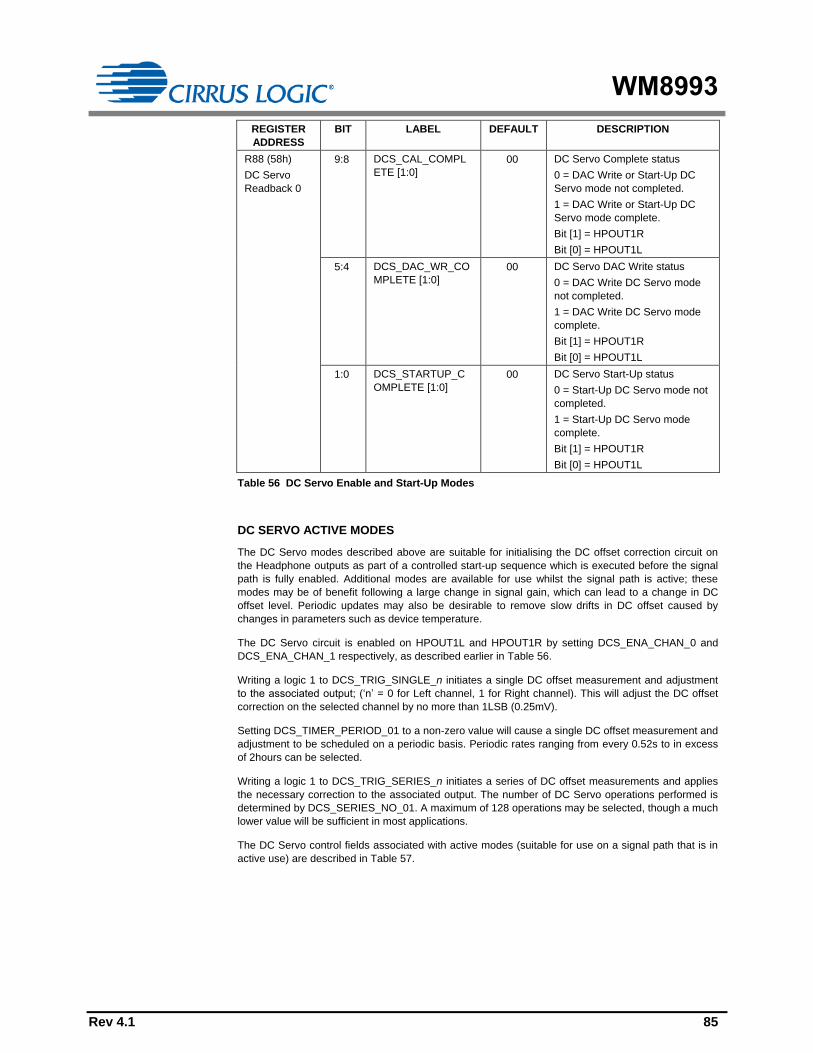
WM8993
Rev 4.1 85
REGISTER
ADDRESS
BIT LABEL DEFAULT DESCRIPTION
R88 (58h)
DC Servo
Readback 0
9:8 DCS_CAL_COMPL
ETE [1:0]
00 DC Servo Complete status
0 = DAC Write or Start-Up DC
Servo mode not completed.
1 = DAC Write or Start-Up DC
Servo mode complete.
Bit [1] = HPOUT1R
Bit [0] = HPOUT1L
5:4 DCS_DAC_WR_CO
MPLETE [1:0]
00 DC Servo DAC Write status
0 = DAC Write DC Servo mode
not completed.
1 = DAC Write DC Servo mode
complete.
Bit [1] = HPOUT1R
Bit [0] = HPOUT1L
1:0 DCS_STARTUP_C
OMPLETE [1:0]
00 DC Servo Start-Up status
0 = Start-Up DC Servo mode not
completed.
1 = Start-Up DC Servo mode
complete.
Bit [1] = HPOUT1R
Bit [0] = HPOUT1L
Table 56 DC Servo Enable and Start-Up Modes
DC SERVO ACTIVE MODES
The DC Servo modes described above are suitable for initialising the DC offset correction circuit on
the Headphone outputs as part of a controlled start-up sequence which is executed before the signal
path is fully enabled. Additional modes are available for use whilst the signal path is active; these
modes may be of benefit following a large change in signal gain, which can lead to a change in DC
offset level. Periodic updates may also be desirable to remove slow drifts in DC offset caused by
changes in parameters such as device temperature.
The DC Servo circuit is enabled on HPOUT1L and HPOUT1R by setting DCS_ENA_CHAN_0 and
DCS_ENA_CHAN_1 respectively, as described earlier in Table 56.
Writing a logic 1 to DCS_TRIG_SINGLE_n initiates a single DC offset measurement and adjustment
to the associated output; (‘n’ = 0 for Left channel, 1 for Right channel). This will adjust the DC offset
correction on the selected channel by no more than 1LSB (0.25mV).
Setting DCS_TIMER_PERIOD_01 to a non-zero value will cause a single DC offset measurement and
adjustment to be scheduled on a periodic basis. Periodic rates ranging from every 0.52s to in excess
of 2hours can be selected.
Writing a logic 1 to DCS_TRIG_SERIES_n initiates a series of DC offset measurements and applies
the necessary correction to the associated output. The number of DC Servo operations performed is
determined by DCS_SERIES_NO_01. A maximum of 128 operations may be selected, though a much
lower value will be sufficient in most applications.
The DC Servo control fields associated with active modes (suitable for use on a signal path that is in
active use) are described in Table 57.

WM8993
Rev 4.1 86
REGISTER
ADDRESS
BIT LABEL DEFAULT DESCRIPTION
R84 (54h)
DC Servo 0
13 DCS_TRIG_SINGLE
_1
0 Writing 1 to this bit selects a
single DC offset correction for
HPOUT1R.
In readback, a value of 1
indicates that the DC Servo
single correction is in progress.
12 DCS_TRIG_SINGLE
_0
0 Writing 1 to this bit selects a
single DC offset correction for
HPOUT1L.
In readback, a value of 1
indicates that the DC Servo
single correction is in progress.
9 DCS_TRIG_SERIES
_1
0 Writing 1 to this bit selects a
series of DC offset corrections
for HPOUT1R.
In readback, a value of 1
indicates that the DC Servo DAC
Write correction is in progress.
8 DCS_TRIG_SERIES
_0
0 Writing 1 to this bit selects a
series of DC offset corrections
for HPOUT1L.
In readback, a value of 1
indicates that the DC Servo DAC
Write correction is in progress.
R85 (55h)
DC Servo 1
11:5 DCS_SERIES_NO_
01 [6:0]
010 1010 Number of DC Servo updates to
perform in a series event.
0 = 1 updates
1 = 2 updates
...
127 = 128 updates
3:0 DCS_TIMER_PERI
OD_01 [3:0]
1010 Time between periodic updates.
Time is calculated as
0.256s x (2^PERIOD)
0000 = Off
0001 = 0.52s
1010 = 266s (4min 26s)
1111 = 8519s (2hr 22s)
Table 57 DC Servo Active Modes
DC SERVO READBACK
The current DC offset value for each Headphone output channel can be read from Registers R89 and
R90, as described in Table 58. Note that these values may form the basis of settings that are
subsequently used by the DC Servo in DAC Write mode.
REGISTER
ADDRESS
BIT LABEL DEFAULT DESCRIPTION
R89 (59h)
DC Servo
Readback 1
7:0 DCS_INTEG_CHAN
_1
0000 0000 Readback value for HPOUT1R.
Two’s complement format.
LSB is 0.25mV.
Range is -32mV to +31.75mV
R90 (5Ah)
DC Servo
Readback 2
7:0 DCS_INTEG_CHAN
_0
0000 0000 Readback value for HPOUT1L.
Two’s complement format.
LSB is 0.25mV.
Range is -32mV to +31.75mV
Table 58 DC Servo Readback

WM8993
Rev 4.1 87
ANALOGUE OUTPUTS
The speaker, headphone, earpiece and line outputs are highly configurable and may be used in many
different ways.
SPEAKER OUTPUT CONFIGURATIONS
The speaker outputs SPKOUTL and SPKOUTR can be driven by either of the speaker mixers,
SPKMIXL or SPKMIXR, or by the low power, differential Direct Voice path from IN2LP/VRXN and
IN2RP/VRXP. Fine volume control is available on the speaker mixer paths using the SPKLVOL and
SPKRVOL PGAs. A boost function is available on both the speaker mixer paths and the Direct Voice
path. For information on the speaker mixing options, refer to the “Output Signal Path” section.
The speaker outputs SPKOUTL and SPKOUTR operate in a BTL configuration in Class AB or Class D
amplifier modes. The default mode is class D but class AB mode can be selected by setting the
SPKOUT_CLASSAB_MODE register bit, as defined in Table 60.
The speaker outputs may be configured in two ways:
1. Stereo Mode – supports up to 1W into stereo 8 BTL loads
2. Mono Mode – supports up to 2W into a single 4 BTL load
Mono mode is selected by applying a logic high input to the SPKMONO pin (E3). For Stereo mode this
pin should be connected to GND. Note that SPKMONO is referenced to DBVDD.
SPEAKER CONFIGURATION SPKMONO PIN (E3)
Stereo Mode GND
Mono Mode DBVDD
Table 59 SPKMONO Pin Function
For mono operation, the P channels, SPKOUTLP and SPKOUTRP should be connected together on
the PCB, and similarly with the N channels, SPKOUTLN and SPKOUTRN. Refer to External
Components Diagram in the ‘Applications Information’ for more details. In this configuration both left
and right speaker drivers should be enabled (SPKOUTL_ENA=1 and SPKOUTR_ENA=1), but path
selection and volume controls are available on left channel only (SPKMIXL, SPKLVOL and
SPKOUTLBOOST).
Note that for applications with a mono 8 speaker it is possible to improve THD performance at
higher power levels by configuring the output in mono mode instead of running either the left of right
channel in stereo mode.
The connections for stereo and mono speaker configurations are shown in Figure 25.
SPKOUTRPSPKOUTRN
SPKOUTLPSPKOUTLN
8Ω
8Ω
4Ω SPKOUTRPSPKOUTRN
SPKOUTLPSPKOUTLN
Figure 25 Mono and Stereo Speaker Output Configuration
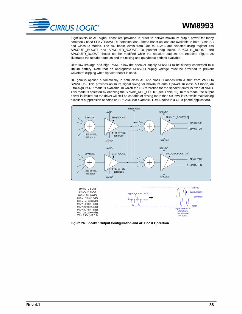
WM8993
Rev 4.1 88
Eight levels of AC signal boost are provided in order to deliver maximum output power for many
commonly-used SPKVDD/AVDD1 combinations. These boost options are available in both Class AB
and Class D modes. The AC boost levels from 0dB to +12dB are selected using register bits
SPKOUTL_BOOST and SPKOUTR_BOOST. To prevent pop noise, SPKOUTL_BOOST and
SPKOUTR_BOOST should not be modified while the speaker outputs are enabled. Figure 26
illustrates the speaker outputs and the mixing and gain/boost options available.
Ultra-low leakage and high PSRR allow the speaker supply SPKVDD to be directly connected to a
lithium battery. Note that an appropriate SPKVDD supply voltage must be provided to prevent
waveform clipping when speaker boost is used.
DC gain is applied automatically in both class AB and class D modes with a shift from VMID to
SPKVDD/2. This provides optimum signal swing for maximum output power. In class AB mode, an
ultra-high PSRR mode is available, in which the DC reference for the speaker driver is fixed at VMID.
This mode is selected by enabling the SPKAB_REF_SEL bit (see Table 60). In this mode, the output
power is limited but the driver will still be capable of driving more than 500mW in 8 while maintaining
excellent suppression of noise on SPKVDD (for example, TDMA noise in a GSM phone application).
SPKOUTL_BOOST[2:0]
SPKOUTL_BOOST
SPKOUTR_BOOST
000 = 1.00x (+0dB)
AGND
SPKVDD/2
SPKVDD
Signal x BOOST
SPKLVOL[6:0]
VMID
AVDD
Signal x BOOST is
automatically
centred around
SPKVDD/2
AVDD
AGND
SPKLMIX
SPKVDD
SPKGND
Direct Voice
SPKOUTLP
SPKOUTLN
000 = 1.19x (+1.5dB)
000 = 1.41x (+3.0dB)
000 = 2.00x (+6.0dB)
000 = 2.37x (+7.5dB)
000 = 1.68x (+4.5dB)
000 = 2.81x (+9.0dB)000 = 3.98x (+12.0dB)
-15dB to 0dB,
3dB steps
-57dB to +6dB,
1dB steps
SPKOUTR_BOOST[2:0]SPKRVOL[6:0]
AVDD
AGND
SPKRMIX
SPKVDD
SPKGND
SPKOUTRP
SPKOUTRN
-15dB to 0dB,
3dB steps
-57dB to +6dB,
1dB steps
Figure 26 Speaker Output Configuration and AC Boost Operation

WM8993
Rev 4.1 89
REGISTER
ADDRESS
BIT LABEL DEFAULT DESCRIPTION
R35 (23h)
SPKMIXR
Attenuation
8 SPKOUT_CLASSAB
_MODE
0b Speaker Class AB Mode Enable
0 = Class D mode
1 = Class AB mode
R37 (25h)
SPKOUT
Boost
5:3 SPKOUTL_BOOST
[2:0]
000b
(1.0x)
Left Speaker Gain Boost
000 = 1.00x boost (+0dB)
001 = 1.19x boost (+1.5dB)
010 = 1.41x boost (+3.0dB)
011 = 1.68x boost (+4.5dB)
100 = 2.00x boost (+6.0dB)
101 = 2.37x boost (+7.5dB)
110 = 2.81x boost (+9.0dB)
111 = 3.98x boost (+12.0dB)
2:0 SPKOUTR_BOOST
[2:0]
000b
(1.0x)
Right Speaker Gain Boost
000 = 1.00x boost (+0dB)
001 = 1.19x boost (+1.5dB)
010 = 1.41x boost (+3.0dB)
011 = 1.68x boost (+4.5dB)
100 = 2.00x boost (+6.0dB)
101 = 2.37x boost (+7.5dB)
110 = 2.81x boost (+9.0dB)
111 = 3.98x boost (+12.0dB)
R54 (36h)
Speaker
Mixer
8 SPKAB_REF_SEL 0b Selects Reference for Speaker in
Class AB mode
0 = SPKVDD/2
1 = VMID
Table 60 Speaker Mode and Boost Control
Clocking of the Class D output driver is derived from CLK_SYS. The clocking frequency division is configured
automatically, according to the CLK_SYS_RATE and SAMPLE_RATE registers. (See “Clocking and Sample
Rates” for further details of the system clocks and control registers.)
The Class D switching clock is enabled whenever SPKOUTL_ENA or SPKOUTR_ENA is set,
provided also that SPKOUT_CLASSAB_MODE = 0. The frequency is as described in Table 61.
Note that the CLK_SYS must be present and enabled when using the speaker outputs in Class D
mode.
SAMPLE
RATE (kHz)
SYSTEM CLOCK RATE (CLK_SYS / fs ratio)
64 128 192 256 384 512 768 1024 1408 1536
8 256 256 256 341.3 256 341.3 256 341.3 352 256
11.025 352.8 352.8 352.8 352.8 352.8 352.8 352.8 352.8
12 384 384 384 384 384 384 384 384
16 256 341.3 384 341.3 384 341.3 384
22.05 352.8 352.8 352.8 352.8 352.8 352.8
24 341.3 384 384 384 384 384
32 341.3 341.3 384 341.3 384
44.1 352.8 352.8 352.8 352.8
48 384 384 384 384
Table 61 Class D Switching Frequency (kHz)

WM8993
Rev 4.1 90
HEADPHONE OUTPUT CONFIGURATIONS
The headphone outputs HPOUT1L andHPOUT1R are driven by the headphone output PGAs
HPOUT1LVOL and HPOUT1RVOL. Each PGA has its own dedicated volume control, as described in
the “Output Signal Path” section. The input to these PGAs can be either the output mixers MIXOUTL
and MIXOUTR or the direct DAC outputs DACL and DACR.
The headphone output driver is capable of driving up to 25mW into a 16Ω or 32Ω load such as a
stereo headset or headphones. The outputs are ground-referenced, eliminating any requirement for
AC coupling capacitors. This is achieved by having separate positive and negative supply rails
powered by an on-chip charge pump. A DC Servo circuit removes any DC offset from the headphone
outputs, suppressing ‘pop’ noise and minimising power consumption. The Charge Pump and DC
Servo are described separately (see “Charge Pump” and “DC Servo” respectively).
It is recommended to connect a zobel network to the headphone output pins HPOUT1L and
HPOUT1R for best audio performance in all applications. The components of the zobel network have
the effect of dampening high frequency oscillations or instabilities that can arise outside the audio
band under certain conditions. Possible sources of these instabilities include the inductive load of a
headphone coil or an active load in the form of an external line amplifier. The capacitance of lengthy
cables or PCB tracks can also lead to amplifier instability. The zobel network should comprise of a
20 resistor and 100nF capacitor in series with each other, as illustrated in Figure 27.
If any ground-referenced headphone output is not used, then the zobel network components can be
omitted from the corresponding output pin, and the pin can be left floating. The respective headphone
driver(s) should not be enabled in this case.
AGND = 0V
WM8993
20Ω
100 nF
AGND = 0V
HPOUT1L
HPOUT1R
HPOUT1FB
20Ω
100 nF
Figure 27 Zobel Network Components for HPOUT1L and HPOUT1R
The headphone output incorporates a common mode, or ground loop, feedback path which provides rejection
of system-related ground noise. The return path is via HPOUT1FB. This pin must be connected to ground for
normal operation of the headphone output. No register configuration is required.
Note that the HPOUT1FB pin should be connected to GND close to the headphone jack, as illustrated in
Figure 27.

WM8993
Rev 4.1 91
EARPIECE DRIVER OUTPUT CONFIGURATIONS
The earpiece driver outputs HPOUT2P and HPOUT2N are driven by the HPOUT2MIX output mixer,
which can take inputs from the mixer output PGAs MIXOUTLVOL and MIXOUTRVOL, or from the low
power, differential Direct Voice path IN2LP/VRXN and IN2RP/VRXP. Fine volume control is available
on the output mixer paths using MIXOUTLVOL and MIXOUTRVOL. A selectable -6dB attenuation is
available on the HPOUT2MIX output, as described in Table 52 (refer to the “Output Signal Path”
section).
The earpiece outputs are designed to operate in a BTL configuration, driving 50mW into a typical 16
ear speaker.
For suppression of pop noise there are two separate enables for the earpiece driver; HPOUT2_ENA
enables the output stage and HPOUT2_IN_ENA enables the mixer and input stage.
HPOUT2_IN_ENA should be enabled a minimum of 50s before HPOUT2_ENA – see “Control Write
Sequencer” section for an example power sequence.
LINE OUTPUT CONFIGURATIONS
The four line outputs LINEOUT1P, LINEOUT1N, LINEOUT2P and LINEOUT2N provide a highly
flexible combination of differential and single-ended configurations, each driven by a dedicated output
mixer. There is a selectable -6dB gain option in each mixer to avoid clipping when mixing more than
one signal into a line output. Additional volume control is available at other locations within each of the
supported signal paths. For more information about the line output mixing options, refer to the “Output
Signal Path” section.
Typical applications for the line outputs (single-ended or differential) are:
Handset or headset microphone output to external voice CODEC
Stereo line output
Output to external speaker driver(s) to support additional loudspeakers (e.g. stereo 2W with
external driver plus on-chip mono 2W output)
When single-ended mode is selected for either LINEOUT1 or LINEOUT2, a buffered VMID must be
enabled as a reference for the outputs. This is enabled by setting the LINEOUT_VMID_BUF_ENA bit
as defined in Table 62.
REGISTER
ADDRESS
BIT LABEL DEFAULT DESCRIPTION
R56 (38h)
AntiPOP1
7 LINEOUT_VMID_BUF_E
NA
0b Enables VMID reference for line
outputs in single-ended mode
0 = Disabled
1 = Enabled
Table 62 LINEOUT VMID Buffer for Single-Ended Operation
Some example line output configurations are listed and illustrated below.
Differential line output from Mic/Line input on IN1L PGA
Differential line output from Mic/Line input on IN1R PGA
Stereo differential line output from output mixers MIXOUTL and MIXOUTR
Stereo single-ended line output from output mixer to either LINEOUT1 or LINEOUT2
Mono single-ended line output from output mixer
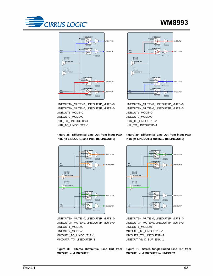
WM8993
Rev 4.1 92
LINEOUT1N
LINEOUT1P+
LINEOUT1NMIX
LINEOUT1PMIX
MIXOUTLVOL
MIXOUTRVOL
Min = -57dB
Max = +6dB
Step = 1dB
Min = -57dB
Max = +6dB
Step = 1dB
0dB or -6dB
0dB or -6dB
LINEOUT2N
LINEOUT2P+
LINEOUT2NMIX
LINEOUT2PMIX
0dB or -6dB
0dB or -6dB
+
+
MIXOUTLVOL
IN1L
IN1R
MIXOUTRVOL
IN1R
IN1L
MIXOUTLVOL
MIXOUTLVOL
IN1L
IN1R
MIXOUTRVOL
IN1R
IN1L
MIXOUTRVOL
IN1L
IN1R
IN1L
IN1R
Ground Loop
Noise Rejection
Ground Loop
Noise Rejection
Ground Loop
Noise Rejection
Ground Loop
Noise Rejection
LINEOUT1N_MUTE=0, LINEOUT1P_MUTE=0
LINEOUT2N_MUTE=0, LINEOUT2P_MUTE=0
LINEOUT1_MODE=0
LINEOUT2_MODE=0
IN1L_TO_LINEOUT1P=1
IN1R_TO_LINEOUT2P=1
LINEOUT1N
LINEOUT1P+
LINEOUT1NMIX
LINEOUT1PMIX
MIXOUTLVOL
MIXOUTRVOL
Min = -57dB
Max = +6dB
Step = 1dB
Min = -57dB
Max = +6dB
Step = 1dB
0dB or -6dB
0dB or -6dB
LINEOUT2N
LINEOUT2P+
LINEOUT2NMIX
LINEOUT2PMIX
0dB or -6dB
0dB or -6dB
+
+
MIXOUTLVOL
IN1L
IN1R
MIXOUTRVOL
IN1R
IN1L
MIXOUTLVOL
MIXOUTLVOL
IN1L
IN1R
MIXOUTRVOL
IN1R
IN1L
MIXOUTRVOL
IN1L
IN1R
IN1L
IN1R
Ground Loop
Noise Rejection
Ground Loop
Noise Rejection
Ground Loop
Noise Rejection
Ground Loop
Noise Rejection
LINEOUT1N_MUTE=0, LINEOUT1P_MUTE=0
LINEOUT2N_MUTE=0, LINEOUT2P_MUTE=0
LINEOUT1_MODE=0
LINEOUT2_MODE=0
IN1R_TO_LINEOUT1P=1
IN1L_TO_LINEOUT2P=1
Figure 28 Differential Line Out from input PGA
IN1L (to LINEOUT1) and IN1R (to LINEOUT2)
Figure 29 Differential Line Out from input PGA
IN1R (to LINEOUT1) and IN1L (to LINEOUT2)
LINEOUT1N
LINEOUT1P+
LINEOUT1NMIX
LINEOUT1PMIX
MIXOUTLVOL
MIXOUTRVOL
Min = -57dB
Max = +6dB
Step = 1dB
Min = -57dB
Max = +6dB
Step = 1dB
0dB or -6dB
0dB or -6dB
LINEOUT2N
LINEOUT2P+
LINEOUT2NMIX
LINEOUT2PMIX
0dB or -6dB
0dB or -6dB
+
+
MIXOUTLVOL
IN1L
IN1R
MIXOUTRVOL
IN1R
IN1L
MIXOUTLVOL
MIXOUTLVOL
IN1L
IN1R
MIXOUTRVOL
IN1R
IN1L
MIXOUTRVOL
IN1L
IN1R
IN1L
IN1R
Ground Loop
Noise Rejection
Ground Loop
Noise Rejection
Ground Loop
Noise Rejection
Ground Loop
Noise Rejection
LINEOUT1N_MUTE=0, LINEOUT1P_MUTE=0
LINEOUT2N_MUTE=0, LINEOUT2P_MUTE=0
LINEOUT1_MODE=0
LINEOUT2_MODE=0
MIXOUTL_TO_LINEOUT1P=1
MIXOUTR_TO_LINEOUT2P=1
LINEOUT1N
LINEOUT1P+
LINEOUT1NMIX
LINEOUT1PMIX
MIXOUTLVOL
MIXOUTRVOL
Min = -57dB
Max = +6dB
Step = 1dB
Min = -57dB
Max = +6dB
Step = 1dB
0dB or -6dB
0dB or -6dB
LINEOUT2N
LINEOUT2P+
LINEOUT2NMIX
LINEOUT2PMIX
0dB or -6dB
0dB or -6dB
+
+
MIXOUTLVOL
IN1L
IN1R
MIXOUTRVOL
IN1R
IN1L
MIXOUTLVOL
MIXOUTLVOL
IN1L
IN1R
MIXOUTRVOL
IN1R
IN1L
MIXOUTRVOL
IN1L
IN1R
IN1L
IN1R
Ground Loop
Noise Rejection
Ground Loop
Noise Rejection
Ground Loop
Noise Rejection
Ground Loop
Noise Rejection
LINEOUT1N_MUTE=0, LINEOUT1P_MUTE=0
LINEOUT2N_MUTE=0, LINEOUT2P_MUTE=0
LINEOUT1_MODE=1
MIXOUTL_TO_LINEOUT1P=1
MIXOUTR_TO_LINEOUT1N=1
LINEOUT_VMID_BUF_ENA=1
Figure 30 Stereo Differential Line Out from
MIXOUTL and MIXOUTR
Figure 31 Stereo Single-Ended Line Out from
MIXOUTL and MIXOUTR to LINEOUT1

WM8993
Rev 4.1 93
LINEOUT1N
LINEOUT1P+
LINEOUT1NMIX
LINEOUT1PMIX
MIXOUTLVOL
MIXOUTRVOL
Min = -57dB
Max = +6dB
Step = 1dB
Min = -57dB
Max = +6dB
Step = 1dB
0dB or -6dB
0dB or -6dB
LINEOUT2N
LINEOUT2P+
LINEOUT2NMIX
LINEOUT2PMIX
0dB or -6dB
0dB or -6dB
+
+
MIXOUTLVOL
IN1L
IN1R
MIXOUTRVOL
IN1R
IN1L
MIXOUTLVOL
MIXOUTLVOL
IN1L
IN1R
MIXOUTRVOL
IN1R
IN1L
MIXOUTRVOL
IN1L
IN1R
IN1L
IN1R
Ground Loop
Noise Rejection
Ground Loop
Noise Rejection
Ground Loop
Noise Rejection
Ground Loop
Noise Rejection
LINEOUT1N_MUTE=0, LINEOUT1P_MUTE=0
LINEOUT2N_MUTE=0, LINEOUT2P_MUTE=0
LINEOUT1_MODE=1
MIXOUTL_TO_LINEOUT2N=1
MIXOUTR_TO_LINEOUT2P=1
LINEOUT_VMID_BUF_ENA=1
LINEOUT1N
LINEOUT1P+
LINEOUT1NMIX
LINEOUT1PMIX
MIXOUTLVOL
MIXOUTRVOL
Min = -57dB
Max = +6dB
Step = 1dB
Min = -57dB
Max = +6dB
Step = 1dB
0dB or -6dB
0dB or -6dB
LINEOUT2N
LINEOUT2P+
LINEOUT2NMIX
LINEOUT2PMIX
0dB or -6dB
0dB or -6dB
+
+
MIXOUTLVOL
IN1L
IN1R
MIXOUTRVOL
IN1R
IN1L
MIXOUTLVOL
MIXOUTLVOL
IN1L
IN1R
MIXOUTRVOL
IN1R
IN1L
MIXOUTRVOL
IN1L
IN1R
IN1L
IN1R
Ground Loop
Noise Rejection
Ground Loop
Noise Rejection
Ground Loop
Noise Rejection
Ground Loop
Noise Rejection
LINEOUT1N_MUTE=0, LINEOUT1P_MUTE=0
LINEOUT2N_MUTE=0, LINEOUT2P_MUTE=0
LINEOUT1_MODE=1
LINEOUT2_MODE=1
MIXOUTL_TO_LINEOUT1N=1 and/or
MIXOUTL_TO_LINEOUT1P=1
MIXOUTR_TO_LINEOUT2N=1 and/or
MIXOUTR_TO_LINEOUT2P=1
LINEOUT_VMID_BUF_ENA=1
Figure 32 Stereo Single-Ended Line Out from
MIXOUTL and MIXOUTR to LINEOUT2
Figure 33 Mono Line Out to LINEOUT1N,
LINEOUT1P, LINEOUT2N, LINEOUT2P
The line outputs incorporate a common mode, or ground loop, feedback path which provides rejection
of system-related ground noise. The return path, via LINEOUTFB, is enabled separately for
LINEOUT1 and LINEOUT2 using the LINEOUT1_FB and LINEOUT2_FB bits as defined in Table 63.
Ground loop feedback is a benefit to single-ended line outputs only; it is not applicable to differential
outputs, which already inherently offer common mode noise rejection.
REGISTER
ADDRESS
BIT LABEL DEFAULT DESCRIPTION
R55 (37h)
Additional
Control
7 LINEOUT1_FB 0b Enable ground loop noise
feedback on LINEOUT1
0 = Disabled
1 = Enabled
6 LINEOUT2_FB 0b Enable ground loop noise
feedback on LINEOUT2
0 = Disabled
1 = Enabled
Table 63 Line Output Ground Loop Feedback Enable
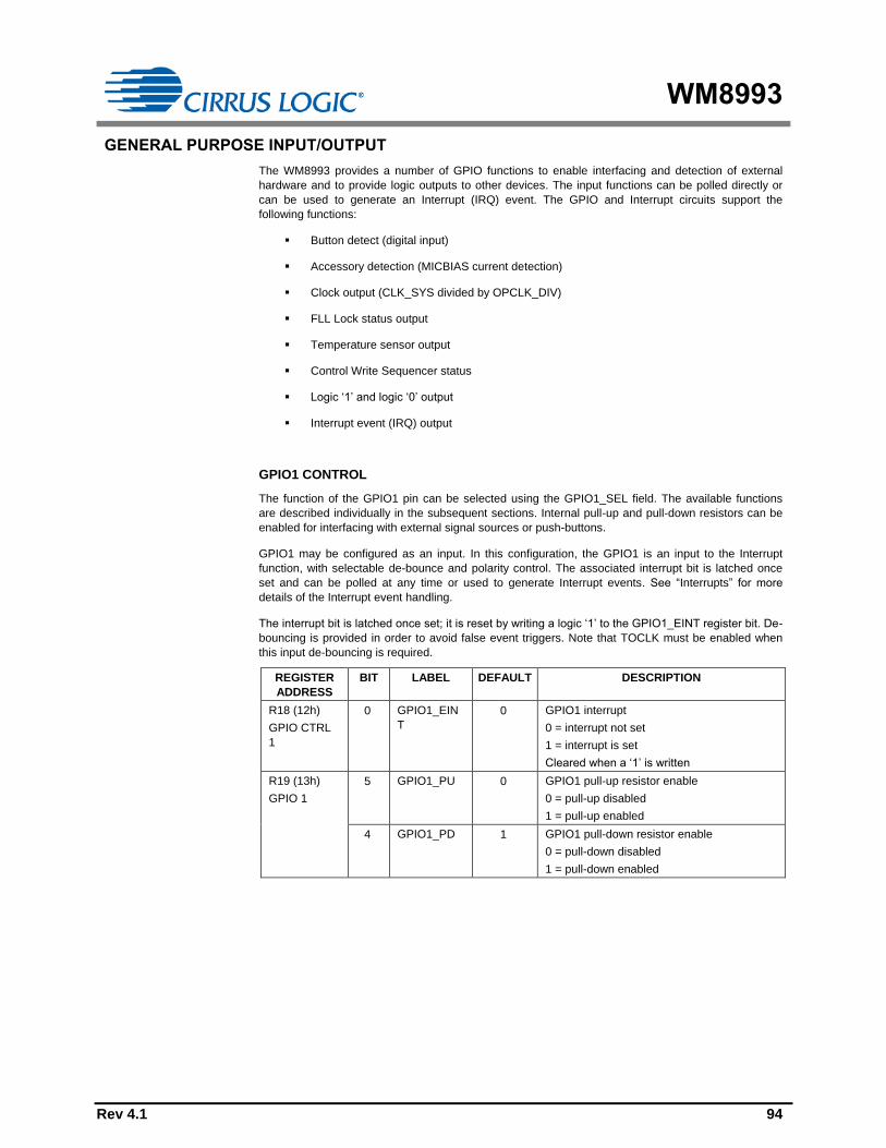
WM8993
Rev 4.1 94
GENERAL PURPOSE INPUT/OUTPUT
The WM8993 provides a number of GPIO functions to enable interfacing and detection of external
hardware and to provide logic outputs to other devices. The input functions can be polled directly or
can be used to generate an Interrupt (IRQ) event. The GPIO and Interrupt circuits support the
following functions:
Button detect (digital input)
Accessory detection (MICBIAS current detection)
Clock output (CLK_SYS divided by OPCLK_DIV)
FLL Lock status output
Temperature sensor output
Control Write Sequencer status
Logic ‘1’ and logic ‘0’ output
Interrupt event (IRQ) output
GPIO1 CONTROL
The function of the GPIO1 pin can be selected using the GPIO1_SEL field. The available functions
are described individually in the subsequent sections. Internal pull-up and pull-down resistors can be
enabled for interfacing with external signal sources or push-buttons.
GPIO1 may be configured as an input. In this configuration, the GPIO1 is an input to the Interrupt
function, with selectable de-bounce and polarity control. The associated interrupt bit is latched once
set and can be polled at any time or used to generate Interrupt events. See “Interrupts” for more
details of the Interrupt event handling.
The interrupt bit is latched once set; it is reset by writing a logic ‘1’ to the GPIO1_EINT register bit. De-
bouncing is provided in order to avoid false event triggers. Note that TOCLK must be enabled when
this input de-bouncing is required.
REGISTER
ADDRESS
BIT LABEL DEFAULT DESCRIPTION
R18 (12h)
GPIO CTRL
1
0 GPIO1_EIN
T
0 GPIO1 interrupt
0 = interrupt not set
1 = interrupt is set
Cleared when a ‘1’ is written
R19 (13h)
GPIO 1
5 GPIO1_PU 0 GPIO1 pull-up resistor enable
0 = pull-up disabled
1 = pull-up enabled
4 GPIO1_PD 1 GPIO1 pull-down resistor enable
0 = pull-down disabled
1 = pull-down enabled

WM8993
Rev 4.1 95
REGISTER
ADDRESS
BIT LABEL DEFAULT DESCRIPTION
3:0 GPIO1_SEL
[3:0]
0000 GPIO1 function select
0000 = GPIO input
0001 = OPCLK
0010 = Logic 0
0011 = Logic 1
0100 = FLL_LOCK
0101 = TEMPOK
0110 = Reserved
0111 = IRQ
1000 = MICBIAS1 current detect
1001 = MICBIAS1 short circuit detect
1010 = MICBIAS2 current detect
1011 = MICBIAS short circuit detect
11XX = Reserved
R20 (14h)
IRQ_DEBOU
NCE
0 GPIO1_DB 0 GPIO1 input de-bounce
0 = disabled
1 = enabled
R22 (16h)
GPIOCTRL2
5 IM_GPIO1_
EINT
0 GPIO1 interrupt mask
0 = do not mask interrupt
1 = mask interrupt
R23 (17h)
GPIO_POL
0 GPIO1_POL 0 GPIO1 interrupt polarity
0 = active high
1 = active low
Table 64 GPIO1 Configuration and Interrupt Control
BUTTON DETECT
The analogue input pins IN2LN and IN2RN support alternate functions as general purpose digital
inputs GPI7 and GPI8 respectively. These digital signals are inputs to the Interrupt function, with
selectable de-bounce and polarity control. The associated interrupt bits are latched once set and can
be polled at any time or used as inputs to the IRQ output. See “Interrupts” for more details of the
Interrupt event handling.
Note that button detect functionality can also be implemented on the GPIO1 pin, as described earlier.
The interrupt bits are latched once set; they are reset by writing a logic ‘1’ to the _EINT register bits in
Register R18 (12h). De-bouncing is provided in order to avoid false event triggers. Note that TOCLK
must be enabled when this input de-bouncing is required.
REGISTER
ADDRESS
BIT LABEL DEFAULT DESCRIPTION
R18 (12h)
GPIO CTRL
1
7 GPI8_EINT 0 GPI8 interrupt
0 = interrupt not set
1 = interrupt is set
Cleared when a ‘1’ is written
6 GPI7_EINT 0 GPI7 interrupt
0 = interrupt not set
1 = interrupt is set
Cleared when a ‘1’ is written
R20 (14h)
IRQ_DEBOU
NCE
7 GPI8_DB 0 GPI8 input de-bounce
0 = disabled
1 = enabled
3 GPI7_DB 0 GPI7 input de-bounce
0 = disabled
1 = enabled

WM8993
Rev 4.1 96
REGISTER
ADDRESS
BIT LABEL DEFAULT DESCRIPTION
R22 (16h)
GPIOCTRL2
6 IM_GPI8_EI
NT
0 GPI8 interrupt mask
0 = do not mask interrupt
1 = mask interrupt
4 GPI8_ENA 0 GPI8 input enable
0 = disabled
1 = enabled
2 IM_GPI7_EI
NT
0 GPI7 interrupt mask
0 = do not mask interrupt
1 = mask interrupt
0 GPI7_ENA 0 GPI7 input enable
0 = disabled
1 = enabled
R23 (17h)
GPIO_POL
7 GPI8_POL 0 GPI8 interrupt polarity
0 = active high
1 = active low
6 GPI7_POL 0 GPI7 interrupt polarity
0 = active high
1 = active low
Table 65 Button Detect Interrupt Control
ACCESSORY DETECTION
Current detection is provided on each of the microphone bias sources MICBIAS1 and MICBIAS2.
These can be configured to detect when an external accessory (such as a microphone) has been
connected. The output voltage of each of the microphone bias sources is selectable. Two current
detection threshold levels can be set; these thresholds are applicable to both microphone bias
sources.
The logic signals from the current detect circuits may be output directly on the GPIO1 pin, and may
also be used to generate Interrupt events. See “GPIO1 Control” for details of outputting the accessory
detection flags on the GPIO1 pin.
The accessory detection circuits are inputs to the Interrupt function, with selectable de-bounce and
polarity control. The associated interrupt bits are latched once set and can be polled at any time or
used as inputs to the IRQ output. See “Interrupts” for more details of the Interrupt event handling.
The interrupt bits are latched once set; they are reset by writing a logic ‘1’ to the _EINT register bits in
Register R18 (12h). De-bouncing is provided in order to avoid false event triggers. Note that TOCLK
must be enabled when this input de-bouncing is required.
REGISTER
ADDRESS
BIT LABEL DEFAULT DESCRIPTION
R1 (1h)
Power
Management
(1)
5 MICB2_ENA 0 Microphone Bias 2 Enable
0 = OFF (high impedance output)
1 = ON
4 MICB1_ENA 0 Microphone Bias 2 Enable
0 = OFF (high impedance output)
1 = ON
R58 (3Ah)
MICBIAS
7:6 JD_SCTHR
[1:0]
00 Jack Detect (MICBIAS) Short Circuit threshold
00 = 300uA
01 = 600uA
10 = 1200uA
11 = 2400uA
These values are for AVDD1=3.0V and scale
proportionally with AVDD1.
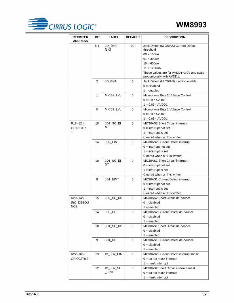
WM8993
Rev 4.1 97
REGISTER
ADDRESS
BIT LABEL DEFAULT DESCRIPTION
5:4 JD_THR
[1:0]
00 Jack Detect (MICBIAS) Current Detect
threshold
00 = 150uA
01 = 300uA
10 = 600uA
11 = 1200uA
These values are for AVDD1=3.0V and scale
proportionally with AVDD1.
2 JD_ENA 0 Jack Detect (MICBIAS) function enable
0 = disabled
1 = enabled
1 MICB2_LVL 0 Microphone Bias 2 Voltage Control
0 = 0.9 * AVDD1
1 = 0.65 * AVDD1
0 MICB1_LVL 0 Microphone Bias 1 Voltage Control
0 = 0.9 * AVDD1
1 = 0.65 * AVDD1
R18 (12h)
GPIO CTRL
1
15 JD2_SC_EI
NT
0 MICBIAS2 Short Circuit interrupt
0 = interrupt not set
1 = interrupt is set
Cleared when a ‘1’ is written
14 JD2_EINT 0 MICBIAS2 Current Detect interrupt
0 = interrupt not set
1 = interrupt is set
Cleared when a ‘1’ is written
10 JD1_SC_EI
NT
0 MICBIAS1 Short Circuit interrupt
0 = interrupt not set
1 = interrupt is set
Cleared when a ‘1’ is written
9 JD1_EINT 0 MICBIAS1 Current Detect interrupt
0 = interrupt not set
1 = interrupt is set
Cleared when a ‘1’ is written
R20 (14h)
IRQ_DEBOU
NCE
15 JD2_SC_DB 0 MICBIAS2 Short Circuit de-bounce
0 = disabled
1 = enabled
14 JD2_DB 0 MICBIAS2 Current Detect de-bounce
0 = disabled
1 = enabled
10 JD1_SC_DB 0 MICBIAS1 Short Circuit de-bounce
0 = disabled
1 = enabled
9 JD1_DB 0 MICBIAS1 Current Detect de-bounce
0 = disabled
1 = enabled
R22 (16h)
GPIOCTRL2
13 IM_JD2_EIN
T
0 MICBIAS2 Current Detect interrupt mask
0 = do not mask interrupt
1 = mask interrupt
12 IM_JD2_SC
_EINT
0 MICBIAS2 Short Circuit interrupt mask
0 = do not mask interrupt
1 = mask interrupt

WM8993
Rev 4.1 98
REGISTER
ADDRESS
BIT LABEL DEFAULT DESCRIPTION
10 IM_JD1_SC
_EINT
0 MICBIAS1 Short Circuit interrupt mask
0 = do not mask interrupt
1 = mask interrupt
9 IM_JD1_EIN
T
0 MICBIAS1 Current Detect interrupt mask
0 = do not mask interrupt
1 = mask interrupt
R23 (17h)
GPIO_POL
15 JD2_SC_PO
L
0 MICBIAS2 Short Circuit interrupt polarity
0 = active high
1 = active low
14 JD2_POL 0 MICBIAS2 Current Detect interrupt polarity
0 = active high
1 = active low
10 JD1_SC_PO
L
0 MICBIAS1 Short Circuit interrupt polarity
0 = active high
1 = active low
9 JD1_POL 0 MICBIAS1 Current Detect interrupt polarity
0 = active high
1 = active low
Table 66 MICBIAS Enable and Interrupt Control
The MICBIAS current detect function is enabled by setting the JD_ENA register bit. When this function
is enabled, two current thresholds can be defined, using the JD_THR and JD_SC_THR registers.
When a change in MICBIAS current which crosses either threshold is detected, then an interrupt
event can be generated. In a typical application, accessory insertion would be detected when the
MICBIAS current exceeds JD_THR, and microphone hookswitch operation would be detected when
the MICBIAS current exceeds JD_SCTHR.
The current detect threshold functions are both inputs to the Interrupt control circuit and can be used
to trigger an Interrupt event when either threshold is crossed. Both events can also be indicated as an
output on a GPIO pin - see “GPIO1 Control”.
When GPIO1_SEL = 1000, 1001, 1010 or 1011, the selected Jack Detect status indication is output
on the GPIO1 pin. A logic 1 indicates that the associated Jack Detect is asserted. Note that the
polarity is not programmable for GPIO output; the GPIO1_POL field and the polarity select bits in
Table 66 affect the Interrupt behaviour only.
In a typical application, microphone insertion would be detected when the MICBIAS current exceeds
the Current Detect threshold set by JD_THR.
When the JDn_POL interrupt polarity bit is set to 0, then microphone insertion detection will cause the
JDn_EINT interrupt status register to be set. (‘n’ = 1 for MICBIAS1, 2 for MICBIAS2.)
For detection of microphone removal, the JDn_POL bit should be set to 1. When the JDn_POL
interrupt polarity bit is set to 1, then microphone removal detection will cause the JDn_EINT interrupt
status register to be set.
Microphone hook switch operation is detected when the MICBIAS current exceeds the Short Circuit
Detect threshold set by JD_SCTHR.
When the JDn_SC_POL interrupt polarity bit is set to 0, then hook switch operation will cause the
JDn_SC_EINT interrupt status register to be set.
For detection of microphone removal, the JDn_SC_POL bit should be set to 1. When the
JDn_SC_POL interrupt polarity bit is set to 1, then hook switch release will cause the JDn_SC_EINT
interrupt status register to be set.

WM8993
Rev 4.1 99
CLOCK OUTPUT
A clock output (OPCLK) derived from CLK_SYS may be output on the GPIO1 pin. This clock is
enabled by register bit OPCLK_ENA, and its frequency is controlled by OPCLK_DIV.
See “Clocking and Sample Rates” for more details of the System Clock, CLK_SYS. See “GPIO1
Control” for details of GPIO1 output of OPCLK.
REGISTER
ADDRESS
BIT LABEL DEFAULT DESCRIPTION
R2 (02h)
Power
Management
(2)
11 OPCLK_EN
A
0b GPIO Clock Output Enable
0 = disabled
1 = enabled
R6 (06h)
Clocking 1
12:9 OPCLK_DIV 0000 GPIO Output Clock Divider
0000 = CLK_SYS
0001 = CLK_SYS / 2
0010 = CLK_SYS / 3
0011 = CLK_SYS / 4
0100 = CLK_SYS / 5.5
0101 = CLK_SYS / 6
0110 = CLK_SYS / 8
0111 = CLK_SYS / 12
1000 = CLK_SYS / 16
1001 to 1111 = Reserved
Table 67 OPCLK Control
FLL LOCK STATUS OUTPUT
The WM8993 maintains a flag indicating the lock status of the FLL, which may be used to control
other events if required. The FLL Lock status may be output directly on the GPIO1 pin, and may also
be used to generate Interrupt events. See “GPIO1 Control” for details of outputting the FLL Lock flag
on the GPIO1 pin. See “Clocking and Sample Rates” for more details of the FLL.
The FLL Lock signal is an input to the Interrupt function, with selectable de-bounce and polarity
control. The associated interrupt bit is latched once set and can be polled at any time or used to
trigger the IRQ output. See “Interrupts” for more details of the Interrupt event handling.
The interrupt bit is latched once set; it is reset by writing a logic ‘1’ to the FLL_LOCK_EINT register bit.
De-bouncing is provided in order to avoid false event triggers. Note that TOCLK must be enabled
when this input de-bouncing is required.
REGISTER
ADDRESS
BIT LABEL DEFAULT DESCRIPTION
R18 (12h)
GPIO CTRL
1
8 FLL_LOCK_
EINT
0 FLL Lock interrupt
0 = interrupt not set
1 = interrupt is set
Cleared when a ‘1’ is written
R20 (14h)
IRQ_DEBOU
NCE
8 FLL_LOCK_
DB
0 FLL Lock de-bounce
0 = disabled
1 = enabled
R22 (16h)
GPIOCTRL2
8 IM_FLL_LO
CK_EINT
0 FLL Lock interrupt mask
0 = do not mask interrupt
1 = mask interrupt
R23 (17h)
GPIO_POL
8 FLL_LOCK_
POL
0 FLL Lock interrupt polarity
0 = active high (interrupt is triggered when
FLL Lock is reached)
1 = active low (interrupt is triggered when FLL
is not locked)
Table 68 FLL Lock Interrupt Control

WM8993
Rev 4.1 100
The FLL Lock signal is asserted when FLL Lock has been reached. When configured to generate an
interrupt event, the default value of FLL_LOCK_POL will cause an interrupt event when FLL Lock has
been reached.
When GPIO1_SEL = 0100, the FLL Lock signal is output on the GPIO1 pin. A logic 1 indicates that
FLL Lock has been reached. Note that the polarity is not programmable for GPIO output; the
GPIO1_POL and FLL_LOCK_POL fields affect the Interrupt behaviour only.
TEMPERATURE SENSOR OUTPUT
The WM8993 incorporates a temperature sensor which detects when the device temperature is within
normal limits or if the device is approaching a hazardous temperature condition. The temperature
status may be output directly on the GPIO1 pin, and may also be used to generate Interrupt events.
See “GPIO1 Control” for details of outputting the Temp OK flag on the GPIO1 pin.
The temperature sensor signal is an input to the Interrupt function, with selectable de-bounce and
polarity control. The associated interrupt bit is latched once set and can be polled at any time or used
to trigger the IRQ output. See “Interrupts” for more details of the Interrupt event handling.
The interrupt bit is latched once set; it is reset by writing a logic ‘1’ to the TEMPOK_EINT register bit.
De-bouncing is provided in order to avoid false event triggers. Note that TOCLK must be enabled
when this input de-bouncing is required.
Note that the temperature sensor can be configured to automatically disable the audio outputs of the
WM8993 (see “Thermal Shutdown”). In some applications, it may be preferable to manage the
temperature sensor event through GPIO or Interrupt functions, allowing a host processor to implement
a controlled system response to an over-temperature condition.
The temperature sensor must be enabled by setting the TSHUT_ENA register bit. When the
TSHUT_OPDIS is also set, then a device over-temperature condition will cause the speaker outputs
(SPKOUTL and SPKOUTR) of the WM8993 to be disabled.
REGISTER
ADDRESS
BIT LABEL DEFAULT DESCRIPTION
R2 (02h)
Power
Management
(2)
14 TSHUT_EN
A
1 Thermal sensor enable
0 = disabled
1 = enabled
13 TSHUT_OP
DIS
1 Thermal shutdown control
(Causes audio outputs to be disabled if an
overtemperature occurs. The thermal sensor
must also be enabled.)
0 = disabled
1 = enabled
R18 (12h)
GPIO CTRL
1
11 TEMPOK_EI
NT
0 Temp OK interrupt
0 = interrupt not set
1 = interrupt is set
Cleared when a ‘1’ is written
R20 (14h)
IRQ_DEBOU
NCE
11 TEMPOK_D
B
0 Temp OK de-bounce
0 = disabled
1 = enabled
R22 (16h)
GPIOCTRL2
11 IM_TEMPO
K_EINT
0 Temp OK interrupt mask
0 = do not mask interrupt
1 = mask interrupt
R23 (17h)
GPIO_POL
11 TEMPOK_P
OL
1 Temp OK interrupt polarity
0 = active high (interrupt is triggered when
temperature is normal)
1 = active low (interrupt is triggered when
over-temperature)
Table 69 Temperature Sensor Enable and Interrupt Control

WM8993
Rev 4.1 101
The Temperature Sensor output is asserted when the device is within normal operating limits. When
configured to generate an interrupt event, the default value of TEMPOK_POL will cause an interrupt
event when an overtemperature condition has been reached.
When GPIO1_SEL = 0101, the Temperature Sensor status is output on the GPIO1 pin. A logic 0
indicates that an overtemperature condition has been reached. Note that the polarity is not
programmable for GPIO output; the GPIO1_POL and TEMPOK_POL fields affect the Interrupt
behaviour only.
CONTROL WRITE SEQUENCER STATUS
The WM8993 Control Write Sequencer (WSEQ) can be used to execute a sequence of register write
operations in response to a simple trigger event. When the Control Write Sequencer is executing a
sequence, normal access to the register map via the Control Interface is restricted. The WM8993
generates a signal indicating the status of the Control Write Sequencer. The WSEQ_BUSY register bit
indicates if the sequencer is busy, or if it has completed the commanded sequence. The WEQ_BUSY
bit can be polled at any time.
The WSEQ_BUSY bit is an input to the GPIO/Interrupt function, with selectable de-bounce and
polarity control. The associated interrupt bit is latched once set and can be used to trigger the IRQ
output. See “Interrupts” for more details of the Interrupt event handling.
The interrupt bit is latched once set; it is reset by writing a logic ‘1’ to the WSEQ_EINT register bit. De-
bouncing is provided in order to avoid false event triggers. Note that TOCLK must be enabled when
this input de-bouncing is required. Note that the read value of WSEQ_EINT is not valid whilst the
Write Sequencer is Busy.
REGISTER
ADDRESS
BIT LABEL DEFAULT DESCRIPTION
R18 (12h)
GPIO CTRL
1
13 WSEQ_EIN
T
0 Write Sequence interrupt
0 = interrupt not set
1 = interrupt is set
Cleared when a ‘1’ is written.
Note that the read value of WSEQ_EINT is
not valid whilst the Write Sequencer is Busy.
R20 (14h)
IRQ_DEBOU
NCE
13 WSEQ_DB 0 Write Sequencer de-bounce
0 = disabled
1 = enabled
R22 (16h)
GPIOCTRL2
1 IM_WSEQ_
EINT
0 Write Sequencer interrupt mask
0 = do not mask interrupt
1 = mask interrupt
R23 (17h)
GPIO_POL
13 WSEQ_POL 0 Write Sequencer interrupt polarity
0 = active high (interrupt is triggered when
WSEQ is busy)
1 = active low (interrupt is triggered when
WSEQ is idle)
R74 (4Ah)
Write
Sequencer 4
0 WSEQ_BUS
Y
0 Sequencer Busy flag (Read Only).
0 = Sequencer idle
1 = Sequencer busy
Note: it is not possible to write to control
registers via the control interface while the
Sequencer is Busy.
Table 70 Control Write Sequencer Interrupt Control
The Control Write Sequencer status output is asserted when the sequencer is busy. In order to
generate an interrupt event indicating that the sequencer has completed its tasks, WSEQ_POL must
be set to ‘1’.

WM8993
Rev 4.1 102
LOGIC ‘1’ AND LOGIC ‘0’ OUTPUT
The GPIO1 pin can be programmed to drive a logic high or logic low signal. See “GPIO1 Control” for
details of GPIO1 register control fields.
INTERRUPTS
The interrupt status flag IRQ is asserted when any un-masked interrupt input is asserted. It represents
the OR’d combination of all the un-masked interrupt inputs. If required, this flag may be inverted using
the IRQ_POL register bit. The IRQ flag can be polled at any time, or may be output directly on the
GPIO1 pin.
An interrupt can be generated by any of the following events described earlier:
Button detect input (on GPIO1, GPI7 or GPI8)
Accessory detection (MICBIAS1 or MICBIAS2 current / short circuit detect)
FLL Lock
Temperature Sensor
Control Write Sequencer
The interrupt events are indicated by the _EINT register fields described earlier. The interrupt event
flags are latched once set; they are reset by writing a logic ‘1’ to the _EINT register bit. Each of these
can be masked as an input to the IRQ function by setting the associated IM_ register field. Note that
the _EINT register fields are always valid, regardless of the setting of the associated IM_ register
fields.
The interrupt behaviour is driven by edge detection (not level detection) of the un-masked inputs.
Therefore, if an input remains asserted after the interrupt register has been reset, then the interrupt
status flag IRQ will not be triggered again. Note that once the IRQ flag is latched then all subsequent
trigger events will be ignored until it has been reset – see Figure 34.
See “GPIO1 Control” for details of outputting IRQ on the GPIO1 pin.
REGISTER
ADDRESS
BIT LABEL DEFAULT DESCRIPTION
R18 (12h)
GPIO CTRL
1
12 IRQ 0 Interrupt status (IRQ)
Polarity is determined by IRQ_POL
This bit is read only.
R23 (17h)
GPIO_POL
12 IRQ_POL 1 Interrupt status (IRQ) polarity
0 = active high
1 = active low
Table 71 Interrupt (IRQ) Control
signal
IRQ
Figure 34 GPIO Latch
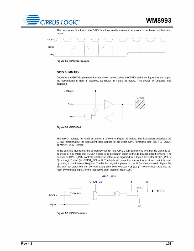
WM8993
Rev 4.1 103
The de-bounce function on the GPIO functions enable transient behaviour to be filtered as illustrated
below:
TOCLK
signal
IRQ
Figure 35 GPIO De-bounce
GPIO SUMMARY
Details of the GPIO implementation are shown below. When the GPIO pad is configured as an output,
the corresponding input is disabled, as shown in Figure 36 below. This avoids an unstable loop
condition.
Enable
Out
In
GPIO1
Figure 36 GPIO Pad
The GPIO register, i.e. latch structure, is shown in Figure 37 below. The illustration describes the
GPIO1 functionality; the equivalent logic applies to the other GPIO functions also (eg. FLL_LOCK,
TEMPOK, Jack Detect).
In the example illustrated, the de-bounce control field GPIO1_DB determines whether the signal is de-
bounced or not. (Note that TOCLK needs to be present in order for the de-bounce circuit to work.) The
polarity bit GPIO1_POL controls whether an interrupt is triggered by a logic 1 level (for GPIO1_POL =
0) or a logic 0 level (for GPIO1_POL = 1). The latch will cause the interrupt to be stored until it is reset
by writing to the Interrupt Register. The latched signal is passed to the IRQ circuit, shown in Figure 38.
The interrupt status bits can be read at any time from Register R18 (12h). The interrupt status bits are
reset by writing a logic 1 to the respective bit in Register R18 (12h).
DebounceTOCLK
GPIO1_DB
signal
GPIO1_POL
wr
en
1 rd
d
latch
to IRQ
Figure 37 GPIO Function
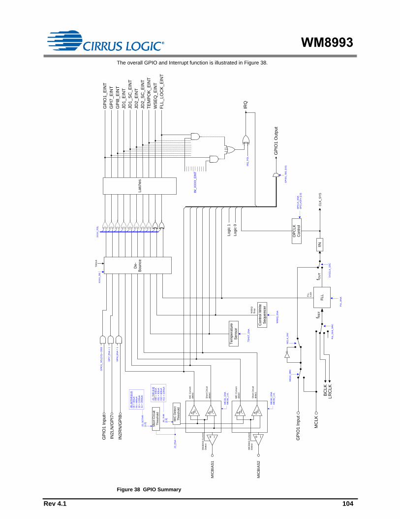
WM8993
Rev 4.1 104
The overall GPIO and Interrupt function is illustrated in Figure 38.
MIC
BIA
S1
IN2LN
/GP
I7
IN2R
N/G
PI8
MIC
BIA
S C
urr
en
t
De
tect
+ - + -
JD
_T
HR
[2
:0]
00
0 =
15
0u
A
00
1 =
30
0u
A
01
0 =
60
0u
A
01
1 =
12
00
uA
Short
Circuit
Thre
shold
MIC
Dete
ct
Thre
shold
JD
_S
CT
HR
[1
:0]
00
= 3
00
uA
01
= 6
00
uA
10
= 1
20
0u
A
11
= 2
40
0u
AJD
_S
CT
HR
[1:0
] JD
_T
HR
[2:0
]
Sh
ort
Circu
it
de
tect
MIC
Cu
rre
nt
de
tect
Tem
pe
ratu
re
Sensor
TS
HU
T_
EN
A
De
-
Boun
ce
TO
CL
K
XX
XX
_D
B
IRQ
_P
OL
GP
IO1_
EIN
T
JD
1_
EIN
T
JD
1_
SC
_E
INT
JD
2_
EIN
T
JD
2_
SC
_E
INT
GP
I7_E
INT
GP
I8_E
INT
TE
MP
OK
_E
INT
IRQ
GP
IO1 O
utp
ut
XX
XX
_P
OL
JD
_E
NA
IM_X
XX
X_E
INT
FLL_
LO
CK
_E
INT
WS
EQ
_E
INT
GP
IO1
_S
EL
[3:0
] =
00
00
Latc
hes
MIC
BIA
S2
MIC
BIA
S C
urr
en
t
De
tect
+ - + -
Sh
ort
Circu
it
de
tect
MIC
Cu
rre
nt
de
tect
MIC
B1
_E
NA
MIC
B1
_L
VL
MIC
B2
_E
NA
MIC
B2
_L
VL
GP
I7_
EN
A =
1
GP
I8_
EN
A =
1
GP
IO1 Inp
ut
MC
LK
FLL
f RE
Ff O
UT
f/N
SY
SC
LK
_S
RC
BC
LK
LR
CLK
FL
L_
CL
K_
SR
C
GP
IO1 Input
MC
LK
_S
RC
MC
LK
_IN
V
FLL_
EN
A
FL
L
Lo
ck
Con
tro
l W
rite
Sequ
ence
r
WS
EQ
_E
NA
WS
EQ
Bu
sy
OP
CLK
Con
tro
lO
PC
LK
_E
NA
OP
CL
KD
IV [
2:0
]
CLK
_S
YS
GP
IO1
_S
EL
[3
:0]
Log
ic 1
Log
ic 0
Figure 38 GPIO Summary

WM8993
Rev 4.1 105
DIGITAL AUDIO INTERFACE
The digital audio interface is used for inputting DAC data to the WM8993 and outputting ADC data
from it. The digital audio interface uses four pins:
ADCDAT: ADC data output
DACDAT: DAC data input
LRCLK: Left/Right data alignment clock
BCLK: Bit clock, for synchronisation
The clock signals BCLK and LRCLK can be outputs when the WM8993 operates as a master, or
inputs when it is a slave (see Master and Slave Mode Operation, below).
Four different audio data formats are supported:
Left justified
Right justified
I2S
DSP mode
All four of these modes are MSB first. They are described in the following sections. Refer to the
“Signal Timing Requirements” section for timing information.
Time Division Multiplexing (TDM) is available in all four data format modes. The WM8993 can be
programmed to send and receive data in one of two time slots.
Two variants of DSP mode are supported - ‘Mode A’ and ‘Mode B’. PCM operation is supported using
the DSP mode.
MASTER AND SLAVE MODE OPERATION
The WM8993 digital audio interface can operate as a master or slave as shown in Figure 39 and
Figure 40.
WM8993 ADCDAT
LRCLK
DACDAT
BCLK
Processor
WM8993 ProcessorADCDAT
LRCLK
DACDAT
BCLK
Figure 39 Master Mode Figure 40 Slave Mode
The Audio Interface output control is illustrated above. The master mode control register AIF_MSTR1
determines whether the WM8993 generates the clock signals. The AIF_MSTR1 register field is
defined in Table 72.
BCLK and LRCLK can be enabled as outputs in Slave mode, allowing mixed Master/Slave operation -
see “Digital Audio Interface Control”.

WM8993
Rev 4.1 106
REGISTER
ADDRESS
BIT LABEL DEFAULT DESCRIPTION
R8 (08h)
Audio
Interface (3)
15 AIF_MSTR1 0 Audio Interface 1 Master Mode Select
0 = Slave mode
1 = Master mode
Table 72 Audio Interface Master/Slave Control
OPERATION WITH TDM
Time division multiplexing (TDM) allows multiple devices to transfer data simultaneously on the same
bus. The WM8993 ADCs and DACs support TDM in master and slave modes for all data formats and
word lengths. TDM is enabled and configured using register bits defined in the “Digital Audio Interface
Control” section.
WM8993 Processor
WM8993 or
Similar
CODEC ADCDAT
ADCLRC
DACDAT
BCLK
ADCDAT
ADCLRC
DACDAT
BCLK
WM8993 Processor
WM8993 or
Similar
CODEC ADCDAT
ADCLRC
DACDAT
BCLK
ADCDAT
ADCLRC
DACDAT
BCLK
Figure 41 TDM with WM8993 as Master Figure 42 TDM with Other CODEC as Master
WM8993 Processor
WM8993 or
Similar
CODEC ADCDAT
ADCLRC
DACDAT
BCLK
ADCDAT
ADCLRC
DACDAT
BCLK
Figure 43 TDM with Processor as Master

WM8993
Rev 4.1 107
Note: The WM8993 is a 24-bit device. If the user operates the WM8993 in 32-bit mode then the 8
LSBs will be ignored on the receiving side and not driven on the transmitting side. It is therefore
recommended to add a pull-down resistor if necessary to the DACDAT line and the ADCDAT line in
TDM mode.
BCLK FREQUENCY
The BCLK frequency is controlled relative to CLK_SYS by the BCLK_DIV divider. Internal clock divide
and phase control mechanisms ensure that the BCLK and LRCLK edges will occur in a predictable
and repeatable position relative to each other and relative to the data for a given combination of
DAC/ADC sample rate and BCLK_DIV settings.
BCLK_DIV is defined in the “Digital Audio Interface Control” section. See also “Clocking and Sample
Rates” section for more information.
AUDIO DATA FORMATS (NORMAL MODE)
The audio data modes supported by the WM8993 are described below. Note that the polarity of the
BCLK and LRCLK signals can be inverted if required; the following descriptions all assume the
default, non-inverted polarity of these signals.
In Right Justified mode, the LSB is available on the last rising edge of BCLK before a LRCLK
transition. All other bits are transmitted before (MSB first). Depending on word length, BCLK frequency
and sample rate, there may be unused BCLK cycles after each LRCLK transition.
nn-1n-2321 nn-1n-2321
LEFT CHANNEL RIGHT CHANNEL
MSB LSBInput Word Length (WL)
1/fs
LRCLK
BCLK
DACDAT/
ADCDAT
Figure 44 Right Justified Audio Interface (assuming n-bit word length)
In Left Justified mode, the MSB is available on the first rising edge of BCLK following a LRCLK
transition. The other bits up to the LSB are then transmitted in order. Depending on word length,
BCLK frequency and sample rate, there may be unused BCLK cycles before each LRCLK transition.
nn-1n-2321 nn-1n-2321
LEFT CHANNEL RIGHT CHANNEL
MSB LSBInput Word Length (WL)
1/fs
LRCLK
BCLK
DACDAT/
ADCDAT
Figure 45 Left Justified Audio Interface (assuming n-bit word length)
In I2S mode, the MSB is available on the second rising edge of BCLK following a LRCLK transition.
The other bits up to the LSB are then transmitted in order. Depending on word length, BCLK

WM8993
Rev 4.1 108
frequency and sample rate, there may be unused BCLK cycles between the LSB of one sample and
the MSB of the next.
nn-1n-2321 nn-1n-2321
LEFT CHANNEL RIGHT CHANNEL
MSB LSBInput Word Length (WL)
1/fs
LRCLK
BCLK
DACDAT/
ADCDAT
1 BCLK 1 BCLK
Figure 46 I2S Justified Audio Interface (assuming n-bit word length)
In DSP mode, the left channel MSB is available on either the 1st (mode B) or 2nd (mode A) rising edge
of BCLK (selectable by AIF_LRCLK_INV) following a rising edge of LRCLK. Right channel data
immediately follows left channel data. Depending on word length, BCLK frequency and sample rate,
there may be unused BCLK cycles between the LSB of the right channel data and the next sample.
In device master mode, the LRC output will resemble the frame pulse shown in Figure 47 and Figure
48. In device slave mode, Figure 49 and Figure 50, it is possible to use any length of frame pulse less
than 1/fs, providing the falling edge of the frame pulse occurs greater than one BCLK period before
the rising edge of the next frame pulse.
nn-1n-2321 nn-1n-2321
LEFT CHANNEL RIGHT CHANNEL
MSB LSBInput Word Length (WL)
1/fs
LRCLK
BCLK
DACDAT/
ADCDAT
1 BCLK
1/2fs
Figure 47 DSP Mode Audio Interface (mode A, AIF_LRCLK_INV=0, Master)
nn-1n-2321 nn-1n-2321
LEFT CHANNEL RIGHT CHANNEL
MSB LSBInput Word Length (WL)
1/fs
LRCLK
BCLK
DACDAT/
ADCDAT
1/2fs
Figure 48 DSP Mode Audio Interface (mode B, AIF_LRCLK_INV=1, Master)

WM8993
Rev 4.1 109
nn-1n-2321 nn-1n-2321
LEFT CHANNEL RIGHT CHANNEL
MSB LSBInput Word Length (WL)
1/fs
LRCLK
BCLK
DACDAT/
ADCDAT
1 BCLK
Falling edge can occur anywhere in this area
1 BCLK
Figure 49 DSP Mode Audio Interface (mode A, AIF_LRCLK_INV=0, Slave)
nn-1n-2321 nn-1n-2321
LEFT CHANNEL RIGHT CHANNEL
MSB LSBInput Word Length (WL)
1/fs
LRCLK
BCLK
DACDAT/
ADCDAT
1 BCLK 1 BCLK
Falling edge can occur anywhere in this area
Figure 50 DSP Mode Audio Interface (mode B, AIF_LRCLK_INV=1, Slave)
PCM operation is supported in DSP interface mode. WM8993 ADC data that is output on the Left
Channel will be read as mono PCM data by the receiving equipment. Mono PCM data received by the
WM8993 will be treated as Left Channel data. This data may be routed to the Left/Right DACs as
described in the “Digital Mixing” section.
AUDIO DATA FORMATS (TDM MODE)
TDM is supported in master and slave mode and is enabled by register bits AIF_ADC_TDM and
AIF_DAC_TDM. All audio interface data formats support time division multiplexing (TDM) for ADC and
DAC data.
Two time slots are available (Slot 0 and Slot 1), selected by register bits AIFADC_TDM_CHAN and
AIFDAC_TDM_CHAN which control time slots for the ADC data and the DAC data.
When TDM is enabled, the ADCDAT pin will be tri-stated immediately before and immediately after
data transmission, to allow another ADC device to drive this signal line for the remainder of the
sample period. Note that it is important that two ADC devices do not attempt to drive the data pin
simultaneously. A short circuit may occur if the transmission time of the two ADC devices overlap with
each other. See “Audio Data Formats (TDM Mode)” for details of the ADCDAT output relative to BCLK
signal. Note that it is possible to ensure a gap exists between transmissions by setting the transmitted
word length to a value higher than the actual length of the data. For example, if 32-bit word length is
selected where only 24-bit data is available, then the WM8993 interface will tri-state after transmission
of the 24-bit data, ensuring a gap after the WM8993’s TDM slot.
When TDM is enabled, BCLK frequency must be high enough to allow data from both time slots to be
transferred. The relative timing of Slot 0 and Slot 1 depends upon the selected data format as shown
in Figure 51 to Figure 55.

WM8993
Rev 4.1 110
SLOT 0
LEFT CHANNEL RIGHT CHANNEL
1/fs
LRCLK
BCLK
DACDAT/
ADCDATSLOT 1 SLOT 0 SLOT 1
Figure 51 TDM in Right-Justified Mode
LEFT CHANNEL RIGHT CHANNEL
1/fs
LRCLK
BCLK
DACDAT/
ADCDATSLOT 0 SLOT 1 SLOT 0 SLOT 1
Figure 52 TDM in Left-Justified Mode
LEFT CHANNEL RIGHT CHANNEL
1/fs
LRCLK
BCLK
DACDAT/
ADCDAT
1 BCLK 1 BCLK
SLOT 0 SLOT 1 SLOT 0 SLOT 1
Figure 53 TDM in I2S Mode
1/fs
LRCLK
BCLK
DACDAT/
ADCDAT
1 BCLK
SLOT 0 LEFT SLOT 0 RIGHT SLOT 1 LEFT SLOT 1 RIGHT
Falling edge can occur anywhere in this area
1 BCLK
Figure 54 TDM in DSP Mode A

WM8993
Rev 4.1 111
1/fs
LRCLK
BCLK
DACDAT/
ADCDAT
1 BCLK
SLOT 0 LEFT SLOT 0 RIGHT SLOT 1 LEFT SLOT 1 RIGHT
Falling edge can occur anywhere in this area
1 BCLK
Figure 55 TDM in DSP Mode B
DIGITAL AUDIO INTERFACE CONTROL
The register bits controlling audio data format, word length, left/right channel data source and TDM
are summarised in Table 73.
REGISTER
ADDRESS
BIT LABEL DEFAULT DESCRIPTION
R4 (04h)
Audio
Interface
(1)
15 AIFADCL_SRC 0 Left Digital Audio interface source
0 = Left ADC data is output on left channel
1 = Right ADC data is output on left channel
14 AIFADCR_SRC 1 Right Digital Audio interface source
0 = Left ADC data is output on right channel
1 = Right ADC data is output on right
channel
13 AIFADC_TDM 0 ADC TDM Enable
0 = Normal ADCDAT operation
1 = TDM enabled on ADCDAT
12 AIFADC_TDM_
CHAN
0 ADCDAT TDM Channel Select
0 = ADCDAT outputs data on slot 0
1 = ADCDAT output data on slot 1
8 AIF_BCLK_INV 0 BCLK Invert
0 = BCLK not inverted
1 = BCLK inverted
Note that AIF_BCLK_INV selects the BCLK
polarity in Master mode and in Slave mode.
7 AIF_LRCLK_IN
V
0 Right, left and I2S modes – LRCLK polarity
0 = normal LRCLK polarity
1 = invert LRCLK polarity
Note that AIF_LRCLK_INV selects the
LRCLK polarity in Master mode and in Slave
mode.
DSP Mode – mode A/B select
0 = MSB is available on 2nd BCLK rising
edge after LRC rising edge (mode A)
1 = MSB is available on 1st BCLK rising
edge after LRC rising edge (mode B)
6:5 AIF_WL [1:0] 10 Digital Audio Interface Word Length
00 = 16 bits
01 = 20 bits
10 = 24 bits
11 = 32 bits
Note - see “Companding” for the selection of
8-bit mode.

WM8993
Rev 4.1 112
REGISTER
ADDRESS
BIT LABEL DEFAULT DESCRIPTION
4:3 AIF_FMT [1:0] 10 Digital Audio Interface Format
00 = Right justified
01 = Left justified
10 = I2S Format
11 = DSP Mode
R5 (05h)
Audio
Interface
(2)
15 AIFDACL_SRC 0 Left DAC Data Source Select
0 = Left DAC outputs left interface data
1 = Left DAC outputs right interface data
14 AIFDACR_SRC 1 Right DAC Data Source Select
0 = Right DAC outputs left interface data
1 = Right DAC outputs right interface data
13 AIFDAC_TDM 0 DAC TDM Enable
0 = Normal DACDAT operation
1 = TDM enabled on DACDAT
12 AIFDAC_TDM_
CHAN
0 DACDAT TDM Channel Select
0 = DACDAT data input on slot 0
1 = DACDAT data input on slot 1
Table 73 Digital Audio Interface Data Control
AUDIO INTERFACE OUTPUT TRI-STATE
Register bit AIF_TRIS can be used to tri-state the audio interface pins as described in Table 74. All
digital audio interface pins will be tri-stated by this function, regardless of the state of other registers
which control these pin configurations.
REGISTER
ADDRESS
BIT LABEL DEFAULT DESCRIPTION
R9 (09h)
Audio
Interface (4)
13 AIF_TRIS 0 Audio Interface Tristate
0 = Audio interface pins operate normally
1 = Tristate all audio interface pins
Table 74 Digital Audio Interface Tri-State Control
BCLK AND LRCLK CONTROL
The audio interface can be programmed to operate in master mode or slave mode using the
AIF_MSTR1 register bit.
In master mode, the BCLK and LRCLK signals are generated by the WM8993 when any of the ADCs
or DACs is enabled. In slave mode, the BCLK and LRCLK clock outputs are disabled by default to
allow another digital audio interface to drive these pins.
It is also possible to force the BCLK or LRCLK signals to be output using BCLK_DIR and
LRCLK_DIR, allowing mixed master and slave modes.
The clock generators for the audio interface are enabled according to the control signals shown in
Figure 56. The BCLK_DIR and LRCLK_DIR fields are defined in Table 75.
The BCLK output can be inverted using the AIF_BCLK_INV register bit. The LRCLK output can be
inverted using the AIF_LRCLK_INV register control.
Note that in Slave mode, when BCLK is an input, the AIF_BCLK_INV register selects the polarity of
the received BCLK signal. Under default conditions, DACDAT input is captured on the rising edge of
BCLK, as illustrated in Figure 4. When AIF_BCLK_INV = 1, DACDAT input is captured on the falling
edge of BCLK.

WM8993
Rev 4.1 113
CLOCK OUTPUT CONTROL
ADCL_ENAADCR_ENA
DACL_ENADACR_ENA BCLK
enable
SYSCLK /BCLKDIV
ADCL_ENAADCR_ENA
DACL_ENADACR_ENA
AIF_MSTR1LRCLK_DIR
BCLK
enable
/LRCLK_RATE LRCLK
AIF_MSTR1BCLK_DIR
Figure 56 Digital Audio Interface Clock Control
REGISTER
ADDRESS
BIT LABEL DEFAULT DESCRIPTION
R4 (04h)
Audio
Interface (1)
9 BCLK_DIR 0 BCLK Direction
(Forces BCLK clock to be output in
slave mode)
0 = BCLK normal operation
1 = BCLK clock output enabled
R6 (06h)
Clocking (1)
4:1 BCLK_DIV 0100 BCLK Rate
0000 = CLK_SYS
0001 = CLK_SYS / 1.5
0010 = CLK_SYS / 2
0011 = CLK_SYS / 3
0100 = CLK_SYS / 4
0101 = CLK_SYS / 5.5
0110 = CLK_SYS / 6
0111 = CLK_SYS / 8
1000 = CLK_SYS / 11
1001 = CLK_SYS / 12
1010 = CLK_SYS / 16
1011 = CLK_SYS / 22
1100 = CLK_SYS / 24
1101 = CLK_SYS / 32
1110 = CLK_SYS / 44
1111 = CLK_SYS / 48
R8 (08h)
Audio
Interface (3)
15 AIF_MSTR1 0 Audio Interface 1 Master Mode Select
0 = Slave mode
1 = Master mode

WM8993
Rev 4.1 114
REGISTER
ADDRESS
BIT LABEL DEFAULT DESCRIPTION
R9 (09h)
Audio
Interface (4)
11 LRCLK_DIR 0 LRCLK Direction
(Forces LRCLK clock to be output in
slave mode)
0 = LRCLK normal operation
1 = LRCLK clock output enabled
10:0 LRCLK_RATE
[10:0]
040h LRCLK Rate
LRCLK clock output =
BCLK / LRCLK_RATE
Integer (LSB = 1)
Valid from 8..2047
Table 75 Digital Audio Interface Clock Control
COMPANDING
The WM8993 supports A-law and -law companding on both transmit (ADC) and receive (DAC) sides
as shown in Table 76.
REGISTER
ADDRESS
BIT LABEL DEFAULT DESCRIPTION
R5 (05h)
Audio
Interface (2)
4 DAC_COMP 0 DAC Companding Enable
0 = disabled
1 = enabled
3 DAC_COMPMODE 0 DAC Companding Type
0 = µ-law
1 = A-law
2 ADC_COMP 0 ADC Companding Enable
0 = disabled
1 = enabled
1 ADC_COMPMODE 0 ADC Companding Type
0 = µ-law
1 = A-law
Table 76 Companding Control
Companding involves using a piecewise linear approximation of the following equations (as set out by
ITU-T G.711 standard) for data compression:
-law (where =255 for the U.S. and Japan):
F(x) = ln( 1 + |x|) / ln( 1 + ) -1 ≤ x ≤ 1
A-law (where A=87.6 for Europe):
F(x) = A|x| / ( 1 + lnA) for x ≤ 1/A
F(x) = ( 1 + lnA|x|) / (1 + lnA) for 1/A ≤ x ≤ 1
The companded data is also inverted as recommended by the G.711 standard (all 8 bits are inverted
for -law, all even data bits are inverted for A-law). The data will be transmitted as the first 8 MSBs of
data.
Companding converts 13 bits (-law) or 12 bits (A-law) to 8 bits using non-linear quantization. This
provides greater precision for low amplitude signals than for high amplitude signals, resulting in a
greater usable dynamic range than 8 bit linear quantization. The companded signal is an 8-bit word
comprising sign (1 bit), exponent (3 bits) and mantissa (4 bits).

WM8993
Rev 4.1 115
8-bit mode is selected whenever DAC_COMP=1 or ADC_COMP=1. The use of 8-bit data allows
samples to be passed using as few as 8 BCLK cycles per LRCLK frame. When using DSP mode B, 8-
bit data words may be transferred consecutively every 8 BCLK cycles.
8-bit mode (without Companding) may be enabled by setting DAC_COMPMODE=1 or
ADC_COMPMODE=1, when DAC_COMP=0 and ADC_COMP=0.
BIT7 BIT[6:4] BIT[3:0]
SIGN EXPONENT MANTISSA
Table 77 8-bit Companded Word Composition
u-law Companding
0
20
40
60
80
100
120
0 0.1 0.2 0.3 0.4 0.5 0.6 0.7 0.8 0.9 1
Normalised Input
Co
mp
an
ded
Ou
tpu
t
0
0.1
0.2
0.3
0.4
0.5
0.6
0.7
0.8
0.9
1
No
rmali
sed
Ou
tpu
t
Figure 57 µ-Law Companding
A-law Companding
0
20
40
60
80
100
120
0 0.2 0.4 0.6 0.8 1
Normalised Input
Co
mp
an
ded
Ou
tpu
t
0
0.1
0.2
0.3
0.4
0.5
0.6
0.7
0.8
0.9
1
No
rmali
sed
Ou
tpu
t
Figure 58 A-Law Companding

WM8993
Rev 4.1 116
LOOPBACK
Setting the LOOPBACK register bit enables digital loopback. When this bit is set, the ADC digital data
output is routed to the DAC digital data input path. The digital audio interface input (DACDAT) is not
used when LOOPBACK is enabled.
REGISTER
ADDRESS
BIT LABEL DEFAULT DESCRIPTION
R5 (05h)
Audio
Interface (2)
0 LOOPBACK 0 Digital Loopback Function
0 = No loopback
1 = Loopback enabled (ADC data output
is directly input to DAC data input).
Table 78 Loopback Control
Note: When the digital sidetone is enabled, ADC data will also be added to DAC digital data input
path within the Digital Mixing circuit. This applies regardless of whether LOOPBACK is enabled.
DIGITAL PULL-UP AND PULL-DOWN
The WM8993 provides integrated pull-up and pull-down resistors on each of the MCLK, DACDAT,
LRCLK and BCLK pins. This provides a flexible capability for interfacing with other devices. Each of
the pull-up and pull-down resistors can be configured independently using the register bits described
in Table 79.
REGISTER
ADDRESS
BIT LABEL DEFAULT DESCRIPTION
R122 (7Ah)
Digital Pulls
7 MCLK_PU 0 MCLK pull-up resistor enable
0 = pull-up disabled
1 = pull-up enabled
6 MCLK_PD 0 MCLK pull-down resistor enable
0 = pull-down disabled
1 = pull-down enabled
5 DACDAT_PU 0 DACDAT pull-up resistor enable
0 = pull-up disabled
1 = pull-up enabled
4 DACDAT_PD 0 DACDAT pull-down resistor enable
0 = pull-down disabled
1 = pull-down enabled
3 LRCLK_PU 0 LRCLK pull-up resistor enable
0 = pull-up disabled
1 = pull-up enabled
2 LRCLK_PD 0 LRCLK pull-down resistor enable
0 = pull-down disabled
1 = pull-down enabled
1 BCLK_PU 0 BCLK pull-up resistor enable
0 = pull-up disabled
1 = pull-up enabled
0 BCLK_PD 0 BCLK pull-down resistor enable
0 = pull-down disabled
1 = pull-down enabled
Table 79 Digital Audio Interface Pull-Up and Pull-Down Control

WM8993
Rev 4.1 117
CLOCKING AND SAMPLE RATES
The internal clocks for the WM8993 are all derived from a common internal clock source, CLK_SYS.
This clock is the reference for the ADCs, DACs, DSP core functions, digital audio interface, Class D
switching amplifier, DC servo control and other internal functions.
CLK_SYS can either be derived directly from MCLK, or may be generated from a Frequency Locked
Loop (FLL) using MCLK, BCLK or LRCLK as a reference. Many commonly-used audio sample rates
can be derived directly from typical MCLK frequencies; the FLL provides additional flexibility for a wide
range of MCLK frequencies. To avoid audible glitches, all clock configurations must be set up before
enabling playback. The FLL can be used to generate a free-running clock in the absence of an
external reference source; see “Frequency Locked Loop (FLL)” for further details.
The WM8993 supports Manual or Automatic clocking configuration modes. In Automatic mode, the
programmable dividers associated with the ADCs, DACs, DSP core functions, Class D switching and
DC servo are configured automatically, with values determined from the CLK_SYS_RATE and
SAMPLE_RATE fields. In Automatic mode, the user must also configure the OPCLK (if required), the
TOCLK (if required) and the digital audio interface. In Manual mode, the entire clocking configuration
can be programmed according to the application requirements.
The ADC and DAC sample rates are independently selectable, relative to CLK_SYS, using ADC_DIV
and DAC_DIV. These fields must be set according to the required sampling frequency. Oversample
rates of 64fs or 128fs are supported (based on a 48kHz sample rate).
A 256kHz clock, supporting a number of internal functions, is derived from CLK_SYS, via a
programmable divider CLK_256K_DIV.
The DC servo control is clocked from CLK_SYS, via a programmable divider CLK_DCS_DIV.
The Class D switching amplifier is clocked from CLK_SYS, via a programmable divider DCLK_DIV.
A GPIO Clock, OPCLK, can be derived from CLK_SYS and output on the GPIO1 pin to provide
clocking to other devices. This clock is enabled by OPCLK_ENA and controlled by OPCLK_DIV.
A slow clock, TOCLK, is used to de-bounce the button/accessory detect inputs, and to set the timeout
period for volume updates when zero-cross detect is used. This clock is enabled by TOCLK_ENA and
controlled by TOCLK_RATE, TOCLK_RATE_X4 and TOCLK_RATE_DIV16.
In master mode, BCLK is derived from CLK_SYS via a programmable divider set by BCLK_DIV. In
master mode, the LRCLK is derived from BCLK via a programmable divider LRCLK_RATE. The
LRCLK can be derived from an internal or external BCLK source, allowing mixed master/slave
operation.
The control registers associated with Clocking and Sample Rates are shown in Table 80 to Table 85.
The overall clocking scheme for the WM8993 is illustrated in Figure 59.

WM8993
Rev 4.1 118
MCLK
FLLfREF fOUT f/N
MCLK
MCLK_SRC selects master clock source (MCLK pin or GPIO1 pin).
FLL
FLL_CLK_SRC selects the input reference for FLL oscillator.
CLK_SYS
Internal clocks are derived from CLK_SYS. These are enabled by CLK_SYS_ENA.
CLK_SYS can be derived from MCLK or from the FLL output. The CLK_SYS source
is selected by SYSCLK_SRC and has a divide by 2 option (MCLKDIV).
CLK_DSP
DSP clocks are derived from CLK_SYS. These are enabled by CLK_DSP_ENA.
DAC Clocks
DAC DSP clock is set by DAC_DIV. This should be set to 256 x Sample Rate in both
master or slave modes. Alternate settings are available using DAC_OSR128 in
Automatic Clocking Control mode only.
ADC Clocks
ADC DSP clock is set by ADC_DIV. This should be set to 256 x Sample Rate in both
master or slave modes. Alternate settings are available using ADC_OSR128.
256kHz Clock
The 256k clock for internal functions is set by CLK_256K_DIV.
DC Servo Clock
DC Servo clock is set by CLK_DCS_DIV. This should be set to around 1.5MHz.
Class D Switching
Class D switching rate is set by DCLK_DIV. This should be set to around 768kHz.
Note that there is an additional divide by two in the output stage producing a 384kHz
switching frequency.
OPCLK Output
GPIO output clock frequency is set by OPCLK_DIV.
TOCLK Control
The slow clock for volume update timeout and GPIO / accessory detect de-bounce is
enabled by TOCLK_ENA. The frequency is set by TOCLK_RATE.
BCLK Rate
BCLK rate is set by BCLK_DIV in master mode. BCLK rate must be high enough to
support the higher of the ADC and DAC sample rates.
LRCLK Rate
LRCLK rate is set by LRCLK_DIV in master mode. The BCLK input to this divider
may be internal or external.
Automatic DSP Clocking Mode
In automatic mode (SR_MODE), most of the clock dividers are configured
automatically by setting the SAMPLE_RATE and CLK_SYS_RATE.
SYSCLK_SRC
CLK_SYS_ENA
BCLKLRCLK
FLL_CLK_SRC R07h[12]
MCLK_DIV
0 = MCLK
1 = MCLK / 2
CLK_DSP_ENA
CLK_DSP
256fs
ADC_DIV [2:0]ADC DSP
64fs or 128fsf/N ADC
R07h[7:5]
ADC_DIV[2:0]
000 = CLK_DSP
001 = CLK_DSP / 1.5
010 = CLK_DSP / 2
011 = CLK_DSP / 3
100 = CLK_DSP / 4
101 = CLK_DSP / 5.5
110 = CLK_DSP / 6
111 = Reserved
f/N
R0Eh[9]
ADC_OSR128
0 = f / 4 (64fs)
1 = f / 2 (128fs)
DAC
DAC_DIV [2:0]
DAC DSP
N.64.fs
R07h[4:2]
DAC_DIV2:0]
000 = CLK_DSP
001 = CLK_DSP / 1.5
010 = CLK_DSP / 2
011 = CLK_DSP / 3
100 = CLK_DSP / 4
101 = CLK_DSP / 5.5
110 = CLK_DSP / 6
111 = Reserved
f/N
Automatic DSP
Clocking Control
SR_MODE
SAMPLE_RATE [2:0]
CLK_SYS_RATE [3:0]
In Automatic DSP Clocking Mode,
the DAC, ADC, 256kHz, DC Servo
and Class D clocks are configured
automatically according to
SAMPLE_RATE and
CLK_SYS_RATE.
· For digital functionality, CLK_SYS minimum is 64fs (DAC mono), 128fs (DAC stereo) or 256fs (ADC).
· For specified noise performance, CLK_SYS minimum is 3MHz (normal mode) or 6MHz (DAC_OSR128 mode).
· DAC_OSR128 mode can be selected in Auto mode, by setting DAC_OSR128.
· The clock divider control fields are ignored and invalid in Auto Mode.
CLK_SYS
DAC_OSR128
R41h[13:10]
CLK_DCS_DIV[3:0]
0000 = CLK_SYS
0001 = CLK_SYS / 1.5
0010 = CLK_SYS / 2
0011 = CLK_SYS / 2.5
0100 = CLK_SYS / 3
0101 = CLK_SYS / 4
0110 = CLK_SYS / 5.5
0111 = CLK_SYS / 6
1000 = CLK_SYS / 8
f/N
CLK_DCS_DIV
DC Servo clock
R06h[8:6]
DCLKDIV[2:0]
000 = CLK_SYS
001 = CLK_SYS / 2
010 = CLK_SYS / 3
011 = CLK_SYS / 4
100 = CLK_SYS / 6
101 = CLK_SYS / 8
110 = CLK_SYS / 12
111 = CLK_SYS / 16
f/N
DCLKDIV
Class D switching clock
GPIO Clock Outputf/N
OPCLK_DIV
R06h[12:9]
OPCLK_DIV[3:0]
0000 = CLK_SYS
0001 = CLK_SYS / 2
0010 = CLK_SYS / 3
0011 = CLK_SYS / 4
0100 = CLK_SYS / 5.5
0101 = CLK_SYS / 6
0110 = CLK_SYS / 8
0111 = CLK_SYS / 12
1000 = CLK_SYS /16
1001 – 1111 = Reserved
OPCLK_ENA
R42h[6:1]
CLK_256K_DIV[5:0]
000000 = CLK_SYS
000001 = CLK_SYS / 2
000010 = CLK_SYS / 3
….
111111 = CLK_SYS / 64
f/N
CLK_256K_DIV
256kHz clock to
Charge Pump and
other circuits
f.N
TOCLK_ENA
Button/accessory
detect de-bounce,
Volume update timeout
f/Nf/1024
R41h[7]
TOCLK_RATE_X4
0 = f x 1
1 = f x 4
R06h[15]
TOCLK_RATE
0 = f / 2
1 = f / 1
f/N
R42h[9]
DAC_DIV4
0 = f / 1
1 = f / 4
N = 1 in Manual mode
N >= 1 in DAC_OSR128 (Auto) mode
N
R06h[4:1]
BCLK_DIV[3:0]
0000 = CLK_SYS
0001 = CLK_SYS / 1.5
0010 = CLK_SYS / 2
0011 = CLK_SYS / 3
0100 = CLK_SYS / 4
0101 = CLK_SYS / 5.5
0110 = CLK_SYS / 6
0111 = CLK_SYS / 8
1000 = CLK_SYS / 11
1001 = CLK_SYS / 12
1010 = CLK_SYS / 16
1011 = CLK_SYS / 22
1100 = CLK_SYS / 24
1101 = CLK_SYS / 32
1110 = CLK_SYS / 44
1111 = CLK_SYS / 48
BCLK_DIV
[3:0]
f/N
LRCLK_RATE
[10:0]
LRCLK
BCLK
MASTER
MODE
CLOCK
OUTPUTSf/N
GPIO1
MCLK_SRC
MCLK_INV
f/N
R41h[8]
TOCLK_RATE_DIV16
0 = f / 1
1 = f / 16
Figure 59 Clocking Scheme

WM8993
Rev 4.1 119
CLK_SYS CONTROL
The MCLK_SRC bit is used to select the MCLK source. The source may be either MCLK or GPIO1.
The selected source may also be inverted by setting the register bit MCLK_INV. Note that it is not
recommended to change the control bit MCLK_INV while the WM8993 is processing data as this may
lead to clocking glitches and signal pop and clicks.
The SYSCLK_SRC bit is used to select the source for CLK_SYS. The source may be either the
selected MCLK source or the FLL output. The selected source may also be adjusted by the
MCLK_DIV divider to generate CLK_SYS. These register fields are described in Table 80. See
“Frequency Locked Loop (FLL)” for more details of the Frequency Locked Loop clock generator.
Note that, in AIF Slave modes (see “Digital Audio Interface”), it is important to ensure that CLK_SYS
is synchronised with the LRCLK input. This can be achieved by selecting an MCLK input that is
derived from the same reference as the LRCLK, or can be achieved by selecting the external BCLK or
LRCLK signals as a reference input to one of the FLLs, as a source for CLK_SYS.
If CLK_SYS is not synchronised with LRCLK, then clicks arising from dropped or repeated audio
samples will occur, due to the inherent tolerances of multiple, asynchronous, system clocks.
The CLK_SYS signal is enabled by register bit CLK_SYS_ENA. This bit should be set to 0 when
reconfiguring clock sources. It is not recommended to change MCLK_SRC or SYSCLK_SRC while
the CLK_SYS_ENA bit is set.
The following operating frequency limits must be observed when configuring CLK_SYS. Failure to
observe these limits will result in degraded noise performance and/or incorrect ADC/DAC functionality.
CLK_SYS ≤ 12.288MHz
CLK_SYS 3MHz
If DAC_OSR128 = 1 (Automatic Mode only), then CLK_SYS 6MHz
If DAC_MONO = 1, then CLK_SYS 64 x fs
If DAC_MONO = 0, then CLK_SYS 128 x fs
If ADCL_ENA = 1 or ADCR_ENA = 1 then CLK_SYS 256 x fs
Note that DAC Mono mode (DAC_MONO = 1) is only valid when one or other DAC is disabled. If both
DACs are enabled, then the minimum CLK_SYS for clocking the DACs is 128 x fs.
The CLK_SYS control register fields are defined in Table 80.
REGISTER
ADDRESS
BIT LABEL DEFAULT DESCRIPTION
R7 (07h)
Clocking 2
15 MCLK_SRC 0 MCLK Source Select
0 = MCLK pin
1 = GPIO1 pin
14 SYSCLK_SRC 0 CLK_SYS Source Select
0 = MCLK
1 = FLL output
12 MCLK_DIV 0 MCLK Divider
0 = MCLK
1 = MCLK / 2
10 MCLK_INV 0b MCLK Invert
0 = MCLK not inverted
1 = MCLK inverted
R69 (45h)
Bus Control
1
1 CLK_SYS_ENA 1 CLK_SYS enable
0 = disabled
1 = enabled
Table 80 MCLK and CLK_SYS Control

WM8993
Rev 4.1 120
AUTOMATIC CLOCKING CONFIGURATION
The WM8993 supports a wide range of standard audio sample rates from 8kHz to 48kHz. The
Automatic Clocking Configuration mode simplifies the configuration of the clock dividers in the
WM8993 by deriving most of the necessary parameters from a minimum number of user registers.
Automatic Clocking Configuration mode is selected by the SR_MODE bit. When Automatic mode is
selected (SR_MODE = 0), some of the Manual clocking configuration registers are invalid and
ignored. The affected registers are indicated in Table 82 and Table 83.
In Automatic mode, the SAMPLE_RATE field selects the sample rate, fs, of the ADC and DAC. Note
that, in Automatic mode, the same sample rate always applies to the ADC and DAC.
In Automatic mode, the CLK_SYS_RATE field must be set according to the ratio of CLK_SYS to fs.
In Automatic mode, a high performance mode of DAC operation can be selected by setting the
DAC_OSR128 bit; in 48kHz sample mode, the DAC_OSR128 feature results in 128x oversampling.
Audio performance is improved, but power consumption is also increased.
In both Manual and Automatic modes, the CLK_SYS_RATE register must be set; this determines the
operating behaviour of the headphone amplifier Charge Pump circuit.
REGISTER
ADDRESS
BIT LABEL DEFAULT DESCRIPTION
R10 (0Ah)
DAC CTRL
13 DAC_OSR128 0 DAC Oversample Rate Select
0 = disabled
1 = enabled
For 48kHz sample rate, the DAC
oversample rate is 128fs when
DAC_OSR128 is selected.
This is valid in Automatic mode only.
The default is 64fs.
R65 (41h)
Clocking 3
9:7 SAMPLE_RATE
[2:0]
101 Selects the Sample Rate (fs)
000 = 8kHz
001 = 11.025kHz, 12kHz
010 = 16kHz
011 = 22.05kHz, 24kHz
100 = 32kHz
101 = 44.1kHz, 48kHz
4:1 CLK_SYS_RAT
E [3:0]
0011 Selects the CLK_SYS / fs ratio
0000 = 64
0001 = 128
0010 = 192
0011 = 256
0100 = 384
0101 = 512
0110 = 768
0111 = 1024
1000 = 1408
1001 = 1536
R66 (42h)
Clocking 4
0 SR_MODE 1 Selects Clocking Configuration mode
0 = Automatic
1 = Manual
Table 81 Automatic Clocking Configuration Control

WM8993
Rev 4.1 121
ADC / DAC CLOCK CONTROL
The clocking of the ADC and DAC circuits is derived from CLK_DSP. This signal is generated from
CLK_SYS and is separately enabled, using the register bit CLK_SYS_ENA.
The ADC and DAC sample rates are independently selectable, relative to CLK_DSP. The
programmable dividers allow selection of the commonly used sample rates from typical audio system
clocking frequencies (eg. 12.288MHz). In Manual Clocking Configuration mode, these are controlled
using the register bits described in Table 82. In Automatic Clocking Configuration mode, the ADC and
DAC clocking dividers are configured automatically by the WM8993.
The ADC_DIV register controls the ADC clocking rate. The ADC_DIV register should be set to derive
256 x fs from CLK_DSP, where fs is the ADC sampling rate (eg. 48kHz).
Two modes of ADC operation can be selected using the ADC_OSR128 bit; in 48kHz sample mode,
setting the ADC_OSR128 bit results in 128x oversampling. This bit is enabled by default, giving best
audio performance. Deselecting this bit gives 64x oversampling in 48kHz mode, resulting in
decreased power consumption.
The DAC_DIV and the DAC_DIV4 registers control the DAC clocking rate. For normal operation,
DAC_DIV4 is set, and the DAC_DIV register should be set to derive 256 x fs from CLK_DSP, where fs
is the DAC sampling rate.
Higher performance DAC operation can be achieved by increasing the DAC oversample rate. This is
available in Automatic Clocking Configuration mode only - see Table 81.
The ADC / DAC Clock Control registers are defined in Table 82.
In Manual Clocking Configuration mode, all of these registers may be controlled.
In Automatic Clocking Configuration mode, the CLK_SYS_ENA field must be set by the user. The
ADC_OSR128 bit may be selected if required. The remaining ADC / DAC Clock Control registers are
ignored and invalid in Automatic mode.
REGISTER
ADDRESS
BIT LABEL DEFAULT DESCRIPTION
R7 (07h)
Clocking 2
7:5 ADC_DIV [2:0] 000 ADC Sample Rate Divider
000 = CLK_SYS / 1
001 = CLK_SYS / 1.5
010 = CLK_SYS / 2
011 = CLK_SYS / 3
100 = CLK_SYS / 4
101 = CLK_SYS / 5.5
110 = CLK_SYS / 6
111= Reserved
Note - this field is ignored and invalid in
Automatic Clocking Configuration mode.
4:2 DAC_DIV [2:0] 000 DAC Sample Rate Divider
000 = CLK_SYS / 1
001 = CLK_SYS / 1.5
010 = CLK_SYS / 2
011 = CLK_SYS / 3
100 = CLK_SYS / 4
101 = CLK_SYS / 5.5
110 = CLK_SYS / 6
111= Reserved
Note - this field is ignored and invalid in
Automatic Clocking Configuration mode.

WM8993
Rev 4.1 122
REGISTER
ADDRESS
BIT LABEL DEFAULT DESCRIPTION
R14 (0Eh)
ADC CTRL
9 ADC_OSR128 1 ADC Oversample Rate Select
0 = disabled
1 = enabled
For 48kHz sample rate, the ADC
oversample rate is 128fs when
ADC_OSR128 is selected. Setting this
bit to 0 selects 64fs mode.
Default is 128fs.
R65 (41h)
Clocking 3
0 CLK_DSP_ENA 0 CLK_DSP enable
0 = disabled
1 = enabled
R66 (42h)
Clocking 4
9 DAC_DIV4 1 DAC Divide-by-4 select
0 = DAC_DIV
1 = DAC_DIV / 4
Note - this field is ignored and invalid in
Automatic Clocking Configuration mode.
Table 82 ADC / DAC Clock Control
256K, DC SERVO, CLASS D CLOCK CONTROL
Clocking is required to support a variety of other functions on the WM8993, including the DC Servo
and the Class D amplifier. In Manual Clocking Configuration mode, these are controlled using the
register bits described in Table 83. In Automatic Clocking Configuration mode, these are configured
automatically by the WM8993.
The DCLK_DIV register controls the Class D amplifier switching frequency. The DCLK_DIV register
should be set to derive a clock frequency of around 768kHz. Note that there is an additional divide by
two in the output stage producing a 384kHz switching frequency. The class D switching clock
frequency should not be altered while the speaker output is active as this may generate an audible
click.
The CLK_DCS_DIV register controls the DC Servo clocking frequency. The CLK_DCS_DIV register
should be set to derive a clock frequency of around 1.5MHz.
The CLK_256K_DIV register controls the 256kHz clocking for other circuits, including the Control
Write Sequencer. The CLK_256K_DIV register should be set to derive a clock frequency of around
256kHz.
REGISTER
ADDRESS
BIT LABEL DEFAULT DESCRIPTION
R6 (06h)
Clocking 1
8:6 DCLK_DIV
[2:0]
111 Class D Clock Divider
000 = CLK_SYS
001 = CLK_SYS / 2
010 = CLK_SYS / 3
011 = CLK_SYS / 4
100 = CLK_SYS / 6
101 = CLK_SYS / 8
110 = CLK_SYS / 12
111 = CLK_SYS / 16
Note - this field is ignored and invalid in
Automatic Clocking Configuration mode.
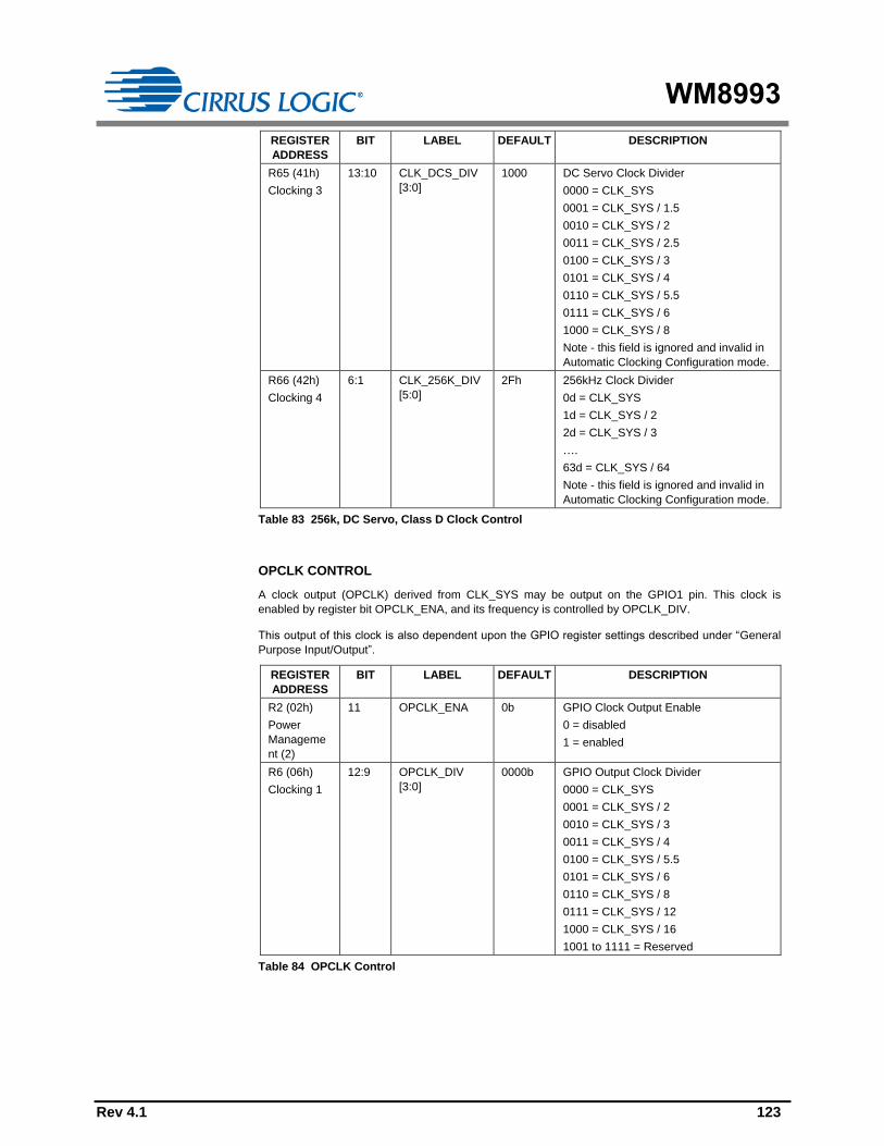
WM8993
Rev 4.1 123
REGISTER
ADDRESS
BIT LABEL DEFAULT DESCRIPTION
R65 (41h)
Clocking 3
13:10 CLK_DCS_DIV
[3:0]
1000 DC Servo Clock Divider
0000 = CLK_SYS
0001 = CLK_SYS / 1.5
0010 = CLK_SYS / 2
0011 = CLK_SYS / 2.5
0100 = CLK_SYS / 3
0101 = CLK_SYS / 4
0110 = CLK_SYS / 5.5
0111 = CLK_SYS / 6
1000 = CLK_SYS / 8
Note - this field is ignored and invalid in
Automatic Clocking Configuration mode.
R66 (42h)
Clocking 4
6:1 CLK_256K_DIV
[5:0]
2Fh 256kHz Clock Divider
0d = CLK_SYS
1d = CLK_SYS / 2
2d = CLK_SYS / 3
….
63d = CLK_SYS / 64
Note - this field is ignored and invalid in
Automatic Clocking Configuration mode.
Table 83 256k, DC Servo, Class D Clock Control
OPCLK CONTROL
A clock output (OPCLK) derived from CLK_SYS may be output on the GPIO1 pin. This clock is
enabled by register bit OPCLK_ENA, and its frequency is controlled by OPCLK_DIV.
This output of this clock is also dependent upon the GPIO register settings described under “General
Purpose Input/Output”.
REGISTER
ADDRESS
BIT LABEL DEFAULT DESCRIPTION
R2 (02h)
Power
Manageme
nt (2)
11 OPCLK_ENA 0b GPIO Clock Output Enable
0 = disabled
1 = enabled
R6 (06h)
Clocking 1
12:9 OPCLK_DIV
[3:0]
0000b GPIO Output Clock Divider
0000 = CLK_SYS
0001 = CLK_SYS / 2
0010 = CLK_SYS / 3
0011 = CLK_SYS / 4
0100 = CLK_SYS / 5.5
0101 = CLK_SYS / 6
0110 = CLK_SYS / 8
0111 = CLK_SYS / 12
1000 = CLK_SYS / 16
1001 to 1111 = Reserved
Table 84 OPCLK Control

WM8993
Rev 4.1 124
TOCLK CONTROL
A slow clock (TOCLK) is derived from the internally generated 256kHz clock to enable input de-
bouncing and volume update timeout functions. This clock is enabled by register bit TOCLK_ENA,
and its frequency is controlled by TOCLK_RATE, TOCLK_RATE_X4, and TOCLK_RATE_DIV16, as
described in Table 85.
A fixed division of 256kHz / 1024 is applied to generate TOCLK. The final TOCLK frequency may be a
multiple or fraction of this frequency, according to the TOCLK_RATE, TOCLK_RATE_X4, and
TOCLK_RATE_DIV16 register bits.
REGISTER
ADDRESS
BIT LABEL DEFAULT DESCRIPTION
R6 (06h)
Clocking 1
15 TOCLK_RATE 0 TOCLK Rate Divider (/2)
0 = f / 2
1 = f / 1
14 TOCLK_ENA 0 TOCLK Enable
0 = disabled
1 = enabled
R66 (42h)
Clocking 4
8 TOCLK_RATE_
DIV16
0 TOCLK Rate Divider (/16)
0 = f / 1
1 = f / 16
7 TOCLK_RATE_
X4
0 TOCLK Rate Multiplier
0 = f x 1
1 = f x 4
Table 85 TOCLK Control
A list of possible TOCLK rates is provided in Table 86.
TOCLK_RATE TOCLK_RATE_X4 TOCLK_RATE_DIV16 TOCLK
FREQ (HZ) PERIOD (MS)
1 1 0 1000 1
0 1 0 500 2
1 0 0 250 4
0 0 0 125 8
1 1 1 62.5 16
0 1 1 31.25 32
1 0 1 15.625 64
0 0 1 7.8125 128
Table 86 TOCLK Rates
BCLK AND LRCLK CONTROL
In master mode, BCLK is derived from CLK_SYS via a programmable division set by BCLK_DIV.
In master mode, LRCLK is derived from BCLK via a programmable division set by LRCLK_RATE. The
BCLK input to this divider may be internal or external, allowing mixed master and slave modes.
The direction of these signals and the clock frequencies are controlled as described in the “Digital
Audio Interface Control” section.

WM8993
Rev 4.1 125
FREQUENCY LOCKED LOOP (FLL)
The integrated FLL can be used to generate CLK_SYS from a wide variety of different reference
sources and frequencies. The FLL can use either MCLK, BCLK or LRCLK as its reference, which may
be a high frequency (eg. 12.288MHz) or low frequency (eg. 32,768kHz) reference. The FLL is tolerant
of jitter and may be used to generate a stable CLK_SYS from a less stable input signal. The FLL
characteristics are summarised in “Electrical Characteristics”.
Note that the FLL can be used to generate a free-running clock in the absence of an external
reference source. This is described in the “Free-Running FLL Clock” section below.
The FLL control registers are illustrated in Figure 60.
FVCO FOUT
90MHz < Fvco < 100MHz
FLL_OUTDIV = 4, 8, 16, 32FLL_FRATIO = 1, 2, 4, 8, 16
Multiply by
N.K
N.K = Real number
Divide by
FLL_CLK_REF_DIV
FREF
FLL_CLK_REF_DIV = 1, 2, 4, 8
FREF<13.5MHz
Divide by
FLL_OUTDIV
Multiply by
FLL_FRATIO
FLL Source
Figure 60 FLL Configuration
The FLL is enabled using the FLL_ENA register bit. Note that, when changing FLL settings, it is
recommended that the digital circuit be disabled via FLL_ENA and then re-enabled after the other
register settings have been updated. When changing the input reference frequency FREF, it is
recommended that the FLL be reset by setting FLL_ENA to 0.
Note that, for normal operation of the FLLs, the reference voltage VMID and the bias current must
also be enabled. See “Reference Voltages and Master Bias” for details of the associated controls
VMID_SEL and BIAS_ENA.
The field FLL_CLK_REF_DIV provides the option to divide the input reference (MCLK, BCLK or
LRCLK) by 1, 2, 4 or 8. This field should be set to bring the reference down to 13.5MHz or below. For
best performance, it is recommended that the highest possible frequency - within the 13.5MHz limit -
should be selected.
The FLL output frequency is directly determined from FLL_FRATIO, FLL_OUTDIV and the real
number represented by N.K. The integer value N is held in the FLL_N register field (LSB = 1), and is
used in both Integer and Fractional Modes. The fractional portion, K, is only valid in Fractional Mode
when enabled by the field FLL_FRAC. It is recommended that FLL_FRAC is enabled at all times.
In FLL Fractional Mode, the fractional portion of the N.K multiplier is held in the FLL_K register field.
This field is coded as a fixed point quantity, where the MSB has a weighting of 0.5. Note that, if
desired, the value of this field may be calculated by multiplying K by 216 and treating FLL_K as an
integer value, as illustrated in the following example:
If N.K = 8.192, then K = 0.192
Multiplying K by 216 gives 0.192 x 65536 = 12582.912 (decimal)
Apply rounding to the nearest integer = 12583 (decimal) = 3127 (hex)
The FLL output frequency is generated according to the following equation:
FOUT = (FVCO / FLL_OUTDIV)
The FLL operating frequency, FVCO is set according to the following equation:
FVCO = (FREF x N.K x FLL_FRATIO)

WM8993
Rev 4.1 126
FREF is the input frequency, as determined by FLL_CLK_REF_DIV.
FVCO must be in the range 90-100 MHz. Frequencies outside this range cannot be supported.
Note that the output frequencies that do not lie within the ranges quoted above cannot be guaranteed
across the full range of device operating temperatures.
In order to follow the above requirements for FVCO, the value of FLL_OUTDIV should be selected
according to the desired output FOUT, as described in Table 87.
OUTPUT FREQUENCY FOUT FLL_OUTDIV
2.8125 MHz - 3.125 MHz 4h (divide by 32)
5.625 MHz - 6.25 MHz 3h (divide by 16)
11.25 MHz - 12.5 MHz 2h (divide by 8)
22.5 MHz - 25 MHz 1h (divide by 4)
Table 87 Selection of FLL_OUTDIV
The value of FLL_FRATIO should be selected as described in Table 88.
REFERENCE FREQUENCY FREF FLL_FRATIO
1MHz - 13.5MHz 0h (divide by 1)
256kHz - 1MHz 1h (divide by 2)
128kHz - 256kHz 2h (divide by 4)
64kHz - 128kHz 3h (divide by 8)
Less than 64kHz 4h (divide by 16)
Table 88 Selection of FLL_FRATIO
In order to determine the remaining FLL parameters, the FLL operating frequency, FVCO, must be
calculated, as given by the following equation:
FVCO = (FOUT x FLL_OUTDIV)
The value of FLL_N and FLL_K can then be determined as follows:
N.K = FVCO / (FLL_FRATIO x FREF)
Note that FREF is the input frequency, after division by FLL_CLK_REF_DIV, where applicable.
For best performance, FLL Fractional Mode should always be used. Therefore, if the calculations yield
an integer value of N.K, then it is recommended to adjust FLL_FRATIO in order to obtain a non-
integer value of N.K.
The register fields that control the FLL are described in Table 89. Example settings for a variety of
reference frequencies and output frequencies are shown in Table 91.

WM8993
Rev 4.1 127
REGISTER
ADDRESS
BIT LABEL DEFAULT DESCRIPTION
R60 (3Ch)
FLL Control 1
2 FLL_FRAC 0 Fractional enable
0 = Integer Mode
1 = Fractional Mode
1 recommended in all cases
1 FLL_OSC_ENA 0 FLL Oscillator Enable
0 = FLL disabled
1 = FLL enabled
(Note that this field is required for
free-running FLL modes only)
0 FLL_ENA 0 FLL Enable
0 = FLL disabled
1 = FLL enabled
R61 (3Dh)
FLL Control 2
10:8 FLL_OUTDIV
[2:0]
000 FOUT clock divider
000 = 2
001 = 4
010 = 8
011 = 16
100 = 32
101 = 64
110 = 128
111 = 256
(FOUT = FVCO / FLL_OUTDIV)
2:0 FLL_FRATIO
[2:0]
000 FVCO clock divider
000 = 1
001 = 2
010 = 4
011 = 8
1XX = 16
R62 (3Eh)
FLL Control 3
15:0 FLL_K[15:0] 0000h Fractional multiply for FREF
(MSB = 0.5)
R63 (3Fh)
FLL Control 4
14:5 FLL_N[9:0] 177h Integer multiply for FREF
(LSB = 1)
R64 (40h)
FLL Control 5
4:3 FLL_CLK_REF_
DIV [1:0]
00b FLL Clock Reference Divider
00 = MCLK / 1
01 = MCLK / 2
10 = MCLK / 4
11 = MCLK / 8
MCLK (or other input reference) must
be divided down to <=13.5MHz.
For lower power operation, the
reference clock can be divided down
further if desired.
1:0 FLL_CLK_SRC
[1:0]
10b FLL Clock source
00 = MCLK
01 = LRCLK
10 = BCLK
11 = Reserved
Table 89 FLL Register Map

WM8993
Rev 4.1 128
FREE-RUNNING FLL CLOCK
The FLL can generate a clock signal even when no external reference is available. However, it should
be noted that the accuracy of this clock is reduced, and a reference source should always be used
where possible. Note that, in free-running modes, the FLL is not sufficiently accurate for hi-fi ADC or
DAC applications. However, the free-running modes are suitable for clocking most other functions,
including the Write Sequencer, Charge Pump, DC Servo and Class D loudspeaker driver.
If an accurate reference clock is initially available, then the FLL should be configured as described
above. The FLL will continue to generate a stable output clock after the reference input is stopped or
disconnected.
If no reference clock is available at the time of starting up the FLL, then an internal clock frequency of
approximately 12MHz can be generated by enabling the FLL Analogue Oscillator using the
FLL_OSC_ENA register bit, and setting FOUT clock divider to divide by 8 (FLL_OUTDIV = 010b), as
defined in Table 89. Under recommended operating conditions, the FLL output may be forced to
approximately 12MHz by then enabling the FLL_FRC_NCO bit and setting FLL_FRC_NCO_VAL to
19h (see Table 90). The resultant CLK_SYS, together with the default settings of DCLK_DIV,
CLK_DCS_DIV and CLK_256K_DIV, delivers the required clock frequencies for the Class D output
driver, DC Servo, Charge Pump and other functions. Note that the value of FLL_FRC_NCO_VAL may
be adjusted to control FOUT, but care should be taken to maintain the correct relationship between
CLK_SYS and the aforementioned functional blocks.
REGISTER
ADDRESS
BIT LABEL DEFAULT DESCRIPTION
R64 (40h)
FLL Control 5
12:7 FLL_FRC_NCO_
VAL
00_0000 Forces the oscillator value
Valid range is 000000 to 111111
0x19h (011001) = 12MHz approx
(Note that this field is required for
free-running FLL modes only)
6 FLL_FRC_NCO 0 FLL control select
0 = controlled by digital loop
(default)
1 = controlled by
FLL_FRC_NCO_VAL
(Note that this field is required for
free-running FLL modes only)
Table 90 FLL Free-Running Mode
In both cases described above, the FLL must be selected as the CLK_SYS source by setting
SYSCLK_SRC (see Table 80). The free-running FLL modes are not sufficiently accurate for hi-fi ADC
or DAC applications. Note that, in the absence of any reference clock, the FLL output is subject to a
very wide tolerance. See “Electrical Characteristics” for details of the FLL accuracy.
EXAMPLE FLL CALCULATION
To generate 12.288 MHz output (FOUT) from a 12.000 MHz reference clock (FREF):
Set FLL_CLK_REF_DIV in order to generate FREF <=13.5MHz:
FLL_CLK_REF_DIV = 00 (divide by 1)
Set FLL_OUTDIV for the required output frequency as shown in Table 87:-
FOUT = 12.288 MHz, therefore FLL_OUTDIV = 2h (divide by 8)
Set FLL_FRATIO for the given reference frequency as shown in Table 88:
FREF = 12MHz, therefore FLL_FRATIO = 0h (divide by 1)
Calculate FVCO as given by FVCO = FOUT x FLL_OUTDIV:-
FVCO = 12.288 x 8 = 98.304MHz
Calculate N.K as given by N.K = FVCO / (FLL_FRATIO x FREF):
N.K = 98.304 / (1 x 12) = 8.192

WM8993
Rev 4.1 129
Determine FLL_N and FLL_K from the integer and fractional portions of N.K:-
FLL_N is 8. FLL_K is 0.192
Confirm that N.K is a fractional quantity and set FLL_FRAC:
N.K is fractional. Set FLL_FRAC = 1.
Note that, if N.K is an integer, then an alternative value of FLL_FRATIO should be selected
in order to produce a fractional value of N.K.
EXAMPLE FLL SETTINGS
Table 91 provides example FLL settings for generating common CLK_SYS frequencies from a variety of low
and high frequency reference inputs.
FREF FOUT FLL_CLK_
REF_DIV
FVCO FLL_N FLL_K FLL_
FRATIO
FLL_
OUTDIV
FLL_
FRAC
32.000
kHz
12.288
MHz
0h
(divide by 1)
98.304
MHz
384
(180h)
0
(0000h)
8
(3h)
8
(2h)
0
32.000
kHz
11.2896
MHz
0h
(divide by 1)
90.3168
MHz
352
(160h)
0.8
(CCCCh)
8
(3h)
8
(2h)
1
32.768
kHz
12.288
MHz
0h
(divide by 1)
98.304
MHz
187
(0BBh)
0.5
(8000h)
16
(4h)
8
(2h)
1
32.768
kHz
11.288576
MHz
0h
(divide by 1)
90.308608
MHz
344
(158h)
0.5
(8000h)
8
(3h)
8
(2h)
1
32.768
kHz
11.2896
MHz
0h
(divide by 1)
90.3168
MHz
344
(158h)
0.53125
(8800h)
8
(3h)
8
(2h)
1
48
kHz
12.288
MHz
0h
(divide by 1)
98.304
MHz
256
(100h)
0
(0000h)
8
(3h)
8
(2h)
0
11.3636
MHz
12.368544
MHz
0h
(divide by 1)
98.948354
MHz
8
(008h)
0.707483
(B51Dh)
1
(0h)
8
(2h)
1
12.000
MHz
12.288
MHz
0h
(divide by 1)
98.3040
MHz
8
(008h)
0.192
(3127h)
1
(0h)
8
(2h)
1
12.000
MHz
11.289597
MHz
0h
(divide by 1)
90.3168
MHz
7
(007h)
0.526398
(86C2h)
1
(0h)
8
(2h)
1
12.288
MHz
12.288
MHz
0h
(divide by 1)
98.304
MHz
8
(008h)
0
(0000h)
1
(0h)
8
(2h)
0
12.288
MHz
11.2896
MHz
0h
(divide by 1)
90.3168
MHz
7
(007h)
0.35
(599Ah)
1
(0h)
8
(2h)
1
13.000
MHz
12.287990
MHz
0h
(divide by 1)
98.3040
MHz
7
(007h)
0.56184
(8FD5h)
1
(0h)
8
(2h)
1
13.000
MHz
11.289606
MHz
0h
(divide by 1)
90.3168
MHz
6
(006h)
0.94745
(F28Ch)
1
(0h)
8
(2h)
1
19.200
MHz
12.287988
MHz
1h
(divide by 2)
98.3039
MHz
5
(005h)
0.119995
(1EB8h)
1
(0h)
8
(2h)
1
19.200
MHz
11.289588
MHz
1h
(divide by 2)
90.3168
MHz
4
(004h)
0.703995
(B439h)
1
(0h)
8
(2h)
1
Table 91 Example FLL Settings

WM8993
Rev 4.1 130
CONTROL INTERFACE
The WM8993 is controlled by writing to registers through a 2-wire serial control interface. Readback is
available for all registers, including device ID, power management status and GPIO status.
The WM8993 is a slave device on the control interface; SCLK is a clock input, while SDAT is a bi-
directional data pin. To allow arbitration of multiple slaves (and/or multiple masters) on the same
interface, the WM8993 transmits logic 1 by tri-stating the SDAT pin, rather than pulling it high. An
external pull-up resistor is required to pull the SDAT line high so that the logic 1 can be recognised by
the master.
In order to allow many devices to share a single 2-wire control bus, every device on the bus has a
unique 7-bit device ID (this is not the same as the 8-bit address of each register in the WM8993). The
WM8993 device ID is 0011 0100 (34h). The LSB of the device ID is the Read/Write bit; this bit is set to
logic 1 for “Read” and logic 0 for “Write”.
The WM8993 operates as a slave device only. The controller indicates the start of data transfer with a
high to low transition on SDAT while SCLK remains high. This indicates that a device ID, register
address and data will follow. The WM8993 responds to the start condition and shifts in the next eight
bits on SDAT (7-bit device ID + Read/Write bit, MSB first). If the device ID received matches the
device ID of the WM8993, then the WM8993 responds by pulling SDAT low on the next clock pulse
(ACK). If the device ID is not recognised or the R/W bit is set incorrectly, the WM8993 returns to the
idle condition and waits for a new start condition and valid address.
If the device ID matches the device ID of the WM8993, the data transfer continues as described
below. The controller indicates the end of data transfer with a low to high transition on SDAT while
SCKL remains high. After receiving a complete address and data sequence the WM8993 returns to
the idle state and waits for another start condition. If a start or stop condition is detected out of
sequence at any point during data transfer (i.e. SDAT changes while SCLK is high), the device returns
to the idle condition.
The WM8993 supports the following read and write operations:
Single write
Single read
Multiple write using auto-increment
Multiple read using auto-increment

WM8993
Rev 4.1 131
The sequence of signals associated with a single register write operation is illustrated in Figure 61.
A1D6 D0 A7SDAT
SCLK
device address data bits B15 – B8
A0 B15 B8 B1 B0
Note: The SDAT pin is used as input for the control register address and data; SDAT
is pulled low by the receiving device to provide the acknowledge (ACK) response
R/W B9 B7
register address data bits B7 – B0START Write ACK ACK ACK STOPACK
Figure 61 Control Interface Register Write
The sequence of signals associated with a single register read operation is illustrated in Figure 62.
A1D7 D1 A7SDAT
SCLK
device ID device ID
A0 D6 B9 B8
Note: The SDA pin is driven by both the master and slave devices in turn to transfer device address, register address, data and ACK responses
R/W D0 B15
register address data bits B15 – B8START (Write) ACK ACK ACK
R/W
(Read)
B1 B0B7
data bits B7 – B0ACK STOPACKRptSTART
Figure 62 Control Interface Register Read
The Control Interface also supports other register operations, as listed above. The interface protocol
for these operations is summarised below. The terminology used in the following figures is detailed in
Table 92.
Note that multiple write and multiple read operations are supported using the auto-increment mode.
This feature enables the host processor to access sequential blocks of the data in the WM8993
register map faster than is possible with single register operations.
TERMINOLOGY DESCRIPTION
S Start Condition
Sr Repeated start
A Acknowledge (SDAT Low)
A Not Acknowledge (SDAT High)
P Stop Condition
R/W ReadNotWrite
0 = Write
1 = Read
[White field] Data flow from bus master to WM8993
[Grey field] Data flow from WM8993 to bus master
Table 92 Control Interface Terminology

WM8993
Rev 4.1 132
Device IDS A Register Address
(0)
A MSByte Data A LSByte Data A PRW
8 bits 8 bits 8 bits 8 bits
Figure 63 Single Register Write to Specified Address
RWDevice IDSr A PMSByte Data
(1)
LSByte DataADevice IDS A Register Address
(0)
ARW A
Figure 64 Single Register Read from Specified Address
Device IDS A Register Address
(0)
A MSByte Data 0 A LSByte Data 0 ARW
Written to 'Register Address'
A MSByte Data N A LSByte Data N A P
Written to 'Register Address+N'
MSByte Data 1
MSByte Data N-2 A MSByte Data N-1 A LSByte Data N-1
Written to 'Register Address+N-1'
Figure 65 Multiple Register Write to Specified Address using Auto-increment
SrDevice IDS A Register Address
(0)
ARW RWDevice ID A
(1)
Read from 'Register Address'
MSByte Data 0 LSByte Data 0A A
PMSByte Data N LSByte Data NA AAMSByte Data N-1 LSByte Data N-1AA
Read from 'Last Register Address+N'Read from 'Last Register Address+N-1'
Figure 66 Multiple Register Read from Specified Address using Auto-increment
RWDevice ID A
PMSByte Data N
(1)
LSByte Data NA
S
AA
MSByte Data 0 LSByte Data 0A A
MSByte Data N-1 LSByte Data N-1AA
Read from 'Last Register Address'
Read from 'Last Register Address+N'Read from 'Last Register Address+N-1'
MSByte Data 1 LSByte Data 1A A
Read from 'Last Register Address+1'
Figure 67 Multiple Register Read from Last Address using Auto-increment

WM8993
Rev 4.1 133
CONTROL WRITE SEQUENCER
The Control Write Sequencer is a programmable unit that forms part of the WM8993 control interface
logic. It provides the ability to perform a sequence of register write operations with the minimum of
demands on the host processor - the sequence may be initiated by a single operation from the host
processor and then left to execute independently.
Default sequences for Start-Up of each output driver and Shut-Down are provided (see “Default
Sequences” section). It is recommended that these default sequences are used unless changes
become necessary.
When a sequence is initiated, the sequencer performs a series of pre-defined register writes. The host
processor informs the sequencer of the start index of the required sequence within the sequencer’s
memory. At each step of the sequence, the contents of the selected register fields are read from the
sequencer’s memory and copied into the WM8993 control registers. This continues sequentially
through the sequencer’s memory until an “End of Sequence” bit is encountered; at this point, the
sequencer stops and an Interrupt status flag is asserted. For cases where the timing of the write
sequence is important, a programmable delay can be set for specific steps within the sequence.
Note that the Control Write Sequencer’s internal clock is derived from the internal clock CLK_SYS
which must be enabled by setting CLK_SYS_ENA (see “Clocking and Sample Rates”). The clock
division from CLK_SYS is handled transparently by the WM8993 without user intervention, as long as
CLK_SYS and sample rates are set correctly.
INITIATING A SEQUENCE
The Register fields associated with running the Control Write Sequencer are described in Table 93.
Note that the operation of the Control Write Sequencer also requires the internal clock CLK_SYS to
be enabled via the CLK_SYS_ENA (see “Clocking and Sample Rates”).
The Write Sequencer is enabled by setting the WSEQ_ENA bit. The start index of the required
sequence must be written to the WSEQ_START_INDEX field. Setting the WSEQ_START bit initiates
the sequencer at the given start index.
The Write Sequencer can be interrupted by writing a logic 1 to the WSEQ_ABORT bit.
The current status of the Write Sequencer can be read using two further register fields - when the
WSEQ_BUSY bit is asserted, this indicates that the Write Sequencer is busy. Note that, whilst the
Control Write Sequencer is running a sequence (indicated by the WSEQ_BUSY bit), normal read/write
operations to the Control Registers cannot be supported. The index of the current step in the Write
Sequencer can be read from the WSEQ_CURRENT_INDEX field; this is an indicator of the
sequencer’s progress. On completion of a sequence, this field holds the index of the last step within
the last commanded sequence.
When the Write Sequencer reaches the end of a sequence, it asserts the WSEQ_EINT flag in
Register R121 (see Table 70). This flag can be used to generate an Interrupt Event on completion of
the sequence. Note that the WSEQ_EINT flag is asserted to indicate that the WSEQ is NOT Busy.
REGISTER
ADDRESS
BIT LABEL DEFAULT DESCRIPTION
R70 (46h)
Write
Sequencer 0
8 WSEQ_ENA 0 Write Sequencer Enable.
0 = Disabled
1 = Enabled
R73 (49h)
Write
Sequencer 3
9 WSEQ_ABORT 0 Writing a 1 to this bit aborts the
current sequence and returns control
of the device back to the serial
control interface.
8 WSEQ_START 0 Writing a 1 to this bit starts the write
sequencer at the memory location
indicated by the
WSEQ_START_INDEX field. The
sequence continues until it reaches
an “End of sequence” flag. At the end
of the sequence, this bit will be reset
by the Write Sequencer.

WM8993
Rev 4.1 134
REGISTER
ADDRESS
BIT LABEL DEFAULT DESCRIPTION
5:0 WSEQ_START_
INDEX [5:0]
00_0000 Sequence Start Index. This is the
memory location of the first command
in the selected sequence.
0 to 31 = RAM addresses
32 to 58 = ROM addresses
59 to 63 = Reserved
R74 (4Ah)
Write
Sequencer 4
0 WSEQ_BUSY
(read only)
0 Sequencer Busy flag (Read Only).
0 = Sequencer idle
1 = Sequencer busy
Note: it is not possible to write to
control registers via the control
interface while the Sequencer is
Busy.
R75 (4Bh)
Write
Sequencer 5
5:0 WSEQ_CURRE
NT_INDEX [5:0]
(read only)
00_0000 Sequence Current Index. This is the
location of the most recently
accessed command in the write
sequencer memory.
Table 93 Write Sequencer Control - Initiating a Sequence
PROGRAMMING A SEQUENCE
A sequence consists of write operations to data bits (or groups of bits) within the control registers. The
Register fields associated with programming the Control Write Sequencer are described in Table 94.
For each step of the sequence being programmed, the Sequencer Index must be written to the
WSEQ_WRITE_INDEX field. The values 0 to 31 correspond to all the available RAM addresses within
the Write Sequencer memory. (Note that memory addresses 32 to 58 also exist, but these are ROM
addresses, which are not programmable.)
Having set the Index as described above, Register R71 must be written to (containing the Control
Register Address, the Start Bit Position and the Field Width applicable to this step of the sequence).
Also, Register R72 must be written to (containing the Register Data, the End of Sequence flag and the
Delay time required after this step is executed). After writing to these two registers, the next step in the
sequence may be programmed by updating WSEQ_WRITE_INDEX and repeating the procedure.
WSEQ_ADDR is an 8-bit field containing the Control Register Address in which the data should be
written.
WSEQ_DATA_START is a 4-bit field which identifies the LSB position within the selected Control
Register to which the data should be written. Setting WSEQ_DATA_START = 0100 will cause 1-bit
data to be written to bit 4. With this setting, 4-bit data would be written to bits 7:4 and so on.
WSEQ_DATA_WIDTH is a 3-bit field which identifies the width of the data block to be written. This
enables selected portions of a Control Register to be updated without any concern for other bits within
the same register, eliminating the need for read-modify-write procedures. Values of 0 to 7 correspond
to data widths of 1 to 8 respectively. For example, setting WSEQ_DATA_WIDTH = 010 will cause a
3-bit data block to be written. Note that the maximum value of this field corresponds to an 8-bit data
block; writing to register fields greater than 8 bits wide must be performed using two separate
operations of the Control Write Sequencer.
WSEQ_DATA is an 8-bit field which contains the data to be written to the selected Control Register.
The WSEQ_DATA_WIDTH field determines how many of these bits are written to the selected
register; the most significant bits (above the number indicated by WSEQ_DATA_WIDTH) are ignored.
WSEQ_DELAY is a 4-bit field which controls the waiting time between the current step and the next
step in the sequence i.e. the delay occurs after the write in which it was called. The total delay time
per step (including execution) is given by:
T = k × (2 WSEQ_DELAY + 8)
where k = 62.5s (under recommended operating conditions)
This gives a useful range of execution/delay times from 562s up to 2.048s per step.

WM8993
Rev 4.1 135
WSEQ_EOS is a 1-bit field which indicates the End of Sequence. If this bit is set, then the Control
Write Sequencer will automatically stop after this step has been executed.
REGISTER
ADDRESS
BIT LABEL DEFAULT DESCRIPTION
R70 (46h)
Write
Sequencer 0
4:0 WSEQ_WRIT
E_INDEX [4:0]
0_0000 Sequence Write Index. This is the
memory location to which any updates to
R71 and R72 will be copied.
0 to 31 = RAM addresses
R71 (47h)
Write
Sequencer 1
14:12 WSEQ_DATA
_WIDTH [2:0]
000 Width of the data block written in this
sequence step.
000 = 1 bit
001 = 2 bits
010 = 3 bits
011 = 4 bits
100 = 5 bits
101 = 6 bits
110 = 7 bits
111 = 8 bits
11:8 WSEQ_DATA
_START [3:0]
0000 Bit position of the LSB of the data block
written in this sequence step.
0000 = Bit 0
…
1111 = Bit 15
7:0 WSEQ_ADDR
[7:0]
0000_0000 Control Register Address to be written to
in this sequence step.
R72 (48h)
Write
Sequencer 2
14 WSEQ_EOS 0 End of Sequence flag. This bit indicates
whether the Control Write Sequencer
should stop after executing this step.
0 = Not end of sequence
1 = End of sequence (Stop the
sequencer after this step).
11:8 WSEQ_DELA
Y [3:0]
0000 Time delay after executing this step.
Total time per step (including execution)
= 62.5µs × (2WSEQ_DELAY + 8)
7:0 WSEQ_DATA
[7:0]
0000_0000 Data to be written in this sequence step.
When the data width is less than 8 bits,
then one or more of the MSBs of
WSEQ_DATA are ignored. It is
recommended that unused bits be set to
0.
Table 94 Write Sequencer Control - Programming a Sequence
Note that a ‘Dummy’ write can be inserted into a control sequence by commanding the sequencer to
write a value of 0 to bit 0 of Register R255 (FFh). This is effectively a write to a non-existent register
location. This can be used in order to create placeholders ready for easy adaptation of the sequence.
For example, a sequence could be defined to power-up a mono signal path from DACL to headphone,
with a ‘dummy’ write included to leave space for easy modification to a stereo signal path
configuration. Dummy writes can also be used in order to implement additional time delays between
register writes. Dummy writes are included in both of the Headphone start-up sequences - see Table
95 and Table 96.
In summary, the Control Register to be written is set by the WSEQ_ADDR field. The data bits that are
written are determined by a combination of WSEQ_DATA_START, WSEQ_DATA_WIDTH and
WSEQ_DATA. This is illustrated below for an example case of writing to the ADCL_DAC_SVOL field
within Register R13 (0Dh).
In this example, the Start Position is bit 09 (WSEQ_DATA_START = 1001b) and the Data width is 4
bits (WSEQ_DATA_WIDTH = 0011b). With these settings, the Control Write Sequencer would update
the Control Register R13 [12:9] with the contents of WSEQ_DATA [3:0].

WM8993
Rev 4.1 136
b15 b14 b13 b12 b11 b10 b09 b08 b07 b06 b05 b04 b03 b02 b01 b00
0ADC_TO_D
ACL
ADC_TO_D
ACR0 0 0
R13 (0Dh)
Digital Side Tone
LSB position = b09
WSEQ_DATA_START = 1001
Data Width = 4 bits
WSEQ_DATA_WIDTH = 0011
WSEQ_DATA (8 bits) b07 b06 b05 b04 b03 b02 b01 b00
WSEQ_DATA_WIDTH = 4 bits.
Therefore, only the Least Significant 4 bits are valid. Bits 04 to 07 are discarded
XXXX
ADCR_DAC_SVOLADCL_DAC_SVOL
Figure 68 Control Write Sequencer Example
DEFAULT SEQUENCES
When the WM8993 is powered up, a number of Control Write Sequences are available through
default settings in both RAM and ROM memory locations. The pre-programmed default settings
include Start-Up and Shut-Down sequences for each of the output drivers. Note that the default
sequences do not include audio signal path or gain setting configuration; this must be implemented
prior to scheduling any of the default Start-Up sequences.
Index addresses 0 to 31 may be programmed to users’ own settings at any time, as described in
“Programming a Sequence”. Users’ own settings remain in memory regardless of WSEQ_ENA, and
are not affected by software resets (i.e. writing to Register R0). However, any non-default sequences
are lost when the device is powered down.
The following default control sequences are provided:
1. Headphone Cold Start-Up - This sequence powers up the headphone driver and charge pump. It
commands the DC Servo to perform offset correction. It enables the master bias required for
analogue functions. This sequence is intended for enabling the headphone output after initial
power-on, when DC offset correction has not previously been run.
2. Headphone Warm Start-Up - This sequence is similar to the Headphone Cold Start-Up, but does
not include the DC Servo operation. This sequence is intended for fast enabling of the
headphone output when DC offset correction has previously been scheduled and provided the
analogue gain settings have not been updated since scheduling the DC offset correction.
3. Speaker Start-Up - This sequence powers up the stereo speaker driver. It also enables the
master bias required for analogue functions.
4. Earpiece Start-Up - This sequence powers up the earpiece driver. It also enables the master bias
required for analogue functions. The soft-start VMID option is used in order to suppress pops
when the driver is enabled. This sequence is intended for enabling the earpiece driver when the
master bias has not previously been enabled.
5. Line Output Start-Up - This sequence powers up the line outputs. Active discharge of the line
outputs is selected, followed by the soft-start VMID enable, followed by selection of the master
bias and un-muting of the line outputs. This sequence is intended for enabling the line drivers
when the master bias has not previously been enabled.
6. Speaker and Headphone Fast Shut-Down - This sequence implements a fast shutdown of the
speaker and headphone drivers. It also disables the DC Servo and charge pump circuits, and

WM8993
Rev 4.1 137
disables the analogue bias circuits using the soft-start (ramp) feature. This sequence is intended
as a shut-down sequence when only the speaker or headphone drivers are enabled.
7. Generic Shut-Down - This sequence shuts down all of the WM8993 output drivers, DC Servo,
charge pump and analogue bias circuits. It is similar to the Fast Shut-Down sequence, with the
additional control of the earpiece and line output drivers. Active discharge of the line outputs is
included and all drivers are disabled as part of this sequence.
Specific details of each of these sequences is provided below.
Headphone Cold Start-Up
The Headphone Cold Start-Up sequence is initiated by writing 0100h to Register 73 (49h). This single
operation starts the Control Write Sequencer at Index Address 0 (00h) and executes the sequence
defined in Table 95.
This sequence takes approximately 296ms to run.
WSEQ
INDEX
REGISTER
ADDRESS
WIDTH START DATA DELAY EOS DESCRIPTION
0 (00h) R57 (39h) 5 bits Bit 2 1Bh 0h 0b STARTUP_BIAS_ENA = 1
VMID_BUF_ENA = 1
VMID_RAMP[1:0] = 11b
(delay = 0.5625ms)
1 (01h) R1 (01h) 3 bits Bit 0 03h 9h 0b BIAS_ENA = 1
VMID_SEL[1:0] = 01b
(delay = 32.5ms)
2 (02h) R76 (4Ch) 1 bits Bit 15 01h 6h 0b CP_ENA = 1
(delay = 4.5ms)
3 (03h) R1 (01h) 3 bits Bit 7 07h 0h 0b HPOUT1R_ENA = 1
HPOUT1L_ENA = 1
(delay = 0.5625ms)
4 (04h) R96 (60h) 5 bits Bit 1 11h 0h 0b HPOUT1R_DLY = 1
HPOUT1L_DLY = 1
(delay = 0.5625ms)
5 (05h) R84 (54h) 6 bits Bit 0 33h Ch 0b DCS_ENA_CHAN_0 = 1
DCS_ENA_CHAN_1 = 1
DCS_TRIG_STARTUP_0 = 1
DCS_TRIG_STARTUP_1 = 1
(delay = 256.5ms)
6 (06h) R255 (FFh) 1 bits Bit 0 00h 0h 0b Dummy Write for expansion
(delay = 0.5625ms)
7 (07h) R96 (60h) 6 bits Bit 2 3Bh 0h 1b HPOUT1R_OUTP = 1
HPOUT1R_RMV_SHORT =1
HPOUT1_DLY = 1
HPOUT1L_OUTP = 1
HPOUT1L_RMV_SHORT = 1
(delay = 0.5625ms)
Table 95 Headphone Cold Start-Up Default Sequence

WM8993
Rev 4.1 138
Headphone Warm Start-Up
The Headphone Warm Start-Up sequence can be initiated by writing 0108h to Register 73 (49h). This
single operation starts the Control Write Sequencer at Index Address 8 (08h) and executes the
sequence defined in Table 96.
This sequence takes approximately 40ms to run.
WSEQ
INDEX
REGISTER
ADDRESS
WIDTH START DATA DELAY EOS DESCRIPTION
8 (08h) R57 (39h) 5 bits Bit 2 1Bh 0h 0b STARTUP_BIAS_ENA = 1
VMID_BUF_ENA = 1
VMID_RAMP[1:0] = 11b
(delay = 0.5625ms)
9 (09h) R1 (01h) 3 bits Bit 0 03h 9h 0b BIAS_ENA = 1
VMID_SEL[1:0] = 01b
(delay = 32.5ms)
10 (0Ah) R76 (4Ch) 1 bits Bit 15 01h 6h 0b CP_ENA = 1
(delay = 4.5ms)
11 (0Bh) R1 (01h) 3 bits Bit 7 07h 0h 0b HPOUT1R_ENA = 1
HPOUT1L_ENA = 1
(delay = 0.5625ms)
12 (0Ch) R96 (60h) 5 bits Bit 1 11h 0h 0b HPOUT1R_DLY = 1
HPOUT1L_DLY = 1
(delay = 0.5625ms)
13 (0Dh) R84 (54h) 2 bits Bit 0 03h 0h 0b DCS_ENA_CHAN_0 = 1
DCS_ENA_CHAN_1 = 1
(delay = 0.5625ms)
14 (0Eh) R255 (FFh) 1 bits Bit 0 00h 0h 0b Dummy Write for expansion
(delay = 0.5625ms)
15 (0Fh) R96 (60h) 6 bits Bit 2 3Bh 0h 1b HPOUT1R_OUTP = 1
HPOUT1R_RMV_SHORT =1
HPOUT1_DLY = 1
HPOUT1L_OUTP = 1
HPOUT1L_RMV_SHORT = 1
(delay = 0.5625ms)
Table 96 Headphone Warm Start-Up Default Sequence

WM8993
Rev 4.1 139
Speaker Start-Up
The Speaker Start-Up sequence can be initiated by writing 0110h to Register 73 (49h). This single
operation starts the Control Write Sequencer at Index Address 16 (10h) and executes the sequence
defined in Table 97.
This sequence takes approximately 34ms to run.
WSEQ
INDEX
REGISTER
ADDRESS
WIDTH START DATA DELAY EOS DESCRIPTION
16 (10h) R57 (39h) 5 bits Bit 2 1Bh 0h 0b STARTUP_BIAS_ENA = 1
VMID_BUF_ENA = 1
VMID_RAMP[1:0] = 11b
(delay = 0.5625ms)
17 (11h) R1 (01h) 3 bits Bit 0 03h 9h 0b BIAS_ENA = 1
VMID_SEL[1:0] = 01b
(delay = 32.5ms)
18 (12h) R1 (01h) 2 bits Bit 12 03h 0h 1b SPKOUTL_ENA = 1
SPKOUTR_ENE = 1
(delay = 0.5625ms)
Table 97 Speaker Start-Up Default Sequence
Earpiece Start-Up
The Earpiece Start-Up sequence can be initiated by writing 0113h to Register 73 (49h). This single
operation starts the Control Write Sequencer at Index Address 19 (13h) and executes the sequence
defined in Table 98.
This sequence takes approximately 259ms to run.
WSEQ
INDEX
REGISTER
ADDRESS
WIDTH START DATA DELAY EOS DESCRIPTION
19 (13h) R57 (39h) 6 bits Bit 1 27h 0h 0b BIAS_SRC = 1
STARTUP_BIAS_ENA = 1
VMID_BUF_ENA = 1
VMID_RAMP[1:0] = 10b
(delay = 0.5625ms)
20 (14h) R56 (38h) 1 bit Bit 6 01h 0h 0b HPOUT2_IN_ENA = 1
(delay = 0.5625ms)
21 (15h) R1 (01h) 1 bit Bit 11 01h 0h 0b HPOUT2_ENA = 1
(delay = 0.5625ms)
22 (16h) R1 (01h) 3 bits Bit 0 03h Ch 0b BIAS_ENA = 1
VMID_SEL[1:0] = 01b
(delay = 256.5ms)
23 (17h) R57 (39h) 1 bit Bit 1 00h 0h 0b BIAS_SRC = 0
(delay = 0.5625ms)
24 (18h) R31 (1Fh) 1 bit Bit 5 00h 0h 1b HPOUT2_MUTE = 0
(delay = 0.5625ms)
Table 98 Earpiece Start-Up Default Sequence

WM8993
Rev 4.1 140
Line Output Start-Up
The Line Output Start-Up sequence can be initiated by writing 0119h to Register 73 (49h). This single
operation starts the Control Write Sequencer at Index Address 25 (19h) and executes the sequence
defined in Table 99.
This sequence takes approximately 517ms to run.
WSEQ
INDEX
REGISTER
ADDRESS
WIDTH START DATA DELAY EOS DESCRIPTION
25 (19h) R56 (38h) 2 bits Bit 4 03h 0h 0b LINEOUT2_DISCH = 1
LINEOUT1_DISCH = 1
(delay = 0.5625ms)
26 (1Ah) R57 (39h) 6 bits Bit 1 27h 0h 0b BIAS_SRC = 1
STARTUP_BIAS_ENA = 1
VMID_BUF_ENA = 1
VMID_RAMP[1:0] = 10b
(delay = 0.5625ms)
27 (1Bh) R56 (38h) 1 bit Bit 7 01h 0h 0b LINEOUT_VMID_BUF_ENA = 1
(delay = 0.5625ms)
28 (1Ch) R3 (03h) 4 bits Bit 10 0Fh 0h 0b LINEOUT2P_ENA = 1
LINEOUT2N_ENA = 1
LINEOUT1P_ENA = 1
LINEOUT1N_ENA = 1
(delay = 0.5625ms)
29 (1Dh) R56 (38h) 2 bits Bit 4 00h 0h 0b LINEOUT2_DISCH = 0
LINEOUT1_DISCH = 0
(delay = 0.5625ms)
30 (1Eh) R1 (01h) 3 bits Bit 0 03h Dh 0b BIAS_ENA = 1
VMID_SEL = 01b
(delay = 0.5625ms)
31 (1Fh) R57 (39h) 1 bit Bit 1 00h 0h 0b BIAS_SRC = 0
(delay = 512.5ms)
32 (20h) R30 (1Eh) 2 bits Bit 5 00h 0h 0b LINEOUT1P_MUTE = 0
LINEOUT1N_MUTE = 0
(delay = 0.5625ms)
33 (21h) R30 (1Eh) 2 bits Bit 1 00h 0h 1b LINEOUT2P_MUTE = 0
LINEOUT2N_MUTE = 0
(delay = 0.5625ms)
Table 99 Line Output Start-Up Default Sequence

WM8993
Rev 4.1 141
Speaker and Headphone Fast Shut-Down
The Speaker and Headphone Fast Shut-Down sequence can be initiated by writing 0122h to Register
73 (49h). This single operation starts the Control Write Sequencer at Index Address 34 (22h) and
executes the sequence defined in Table 100.
This sequence takes approximately 37ms to run.
WSEQ
INDEX
REGISTER
ADDRESS
WIDTH START DATA DELAY EOS DESCRIPTION
34 (22h) R96 (60h) 7 bits Bit 1 00h 0h 0b HPOUT1R_DLY = 0
HPOUT1R_OUTP = 0
HPOUT1R_RMV_SHORT = 0
HPOUT1L_DLY = 0
HPOUT1L_OUTP = 0
HPOUT1L_RMV_SHORT = 0
(delay = 0.5625ms)
35 (23h) R84 (54h) 2 bits Bit 0 00h 0h 0b DCS_ENA_CHAN_0 = 0
DCS_ENA_CHAN_1 = 0
(delay = 0.5625ms)
36 (24h) R1 (01h) 2 bits Bit 8 00h 0h 0b HPOUT1R_ENA = 0
HPOUT1L_ENA = 0
(delay = 0.5625ms)
37 (25h) R76 (4Ch) 1 bit Bit 15 00h 0h 0b CP_ENA = 0
(delay = 0.5625ms)
38 (26h) R1 (01h) 2 bits Bit 12 00h 0h 0b SPKOUTL_ENA = 0
SPKOUTR_ENA = 0
(delay = 0.5625ms)
39 (27h) R57 (39h) 6 bits Bit 1 37h 0h 0b BIAS_SRC = 1
STARTUP_BIAS_ENA = 1
VMID_BUF_ENA = 1
VMID_RAMP[1:0] = 11b
(delay = 0.5625ms)
40 (28h) R1 (01h) 3 bits Bit 0 00h 9h 0b BIAS_ENA = 0
VMID_SEL = 00b
(delay = 32.5ms)
41 (29h) R57 (39h) 6 bits Bit 1 00h 0h 1b BIAS_SRC = 0
STARTUP_BIAS_ENA = 0
VMID_BUF_ENA = 0
VMID_RAMP[1:0] = 00b
(delay = 0.5625ms)
Table 100 Speaker and Headphone Fast Shut-Down Default Sequence
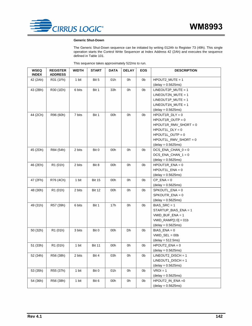
WM8993
Rev 4.1 142
Generic Shut-Down
The Generic Shut-Down sequence can be initiated by writing 012Ah to Register 73 (49h). This single
operation starts the Control Write Sequencer at Index Address 42 (2Ah) and executes the sequence
defined in Table 101.
This sequence takes approximately 522ms to run.
WSEQ
INDEX
REGISTER
ADDRESS
WIDTH START DATA DELAY EOS DESCRIPTION
42 (2Ah) R31 (1Fh) 1 bit Bit 5 01h 0h 0b HPOUT2_MUTE = 1
(delay = 0.5625ms)
43 (2Bh) R30 (1Eh) 6 bits Bit 1 33h 0h 0b LINEOUT2P_MUTE = 1
LINEOUT2N_MUTE = 1
LINEOUT1P_MUTE = 1
LINEOUT1N_MUTE = 1
(delay = 0.5625ms)
44 (2Ch) R96 (60h) 7 bits Bit 1 00h 0h 0b HPOUT1R_DLY = 0
HPOUT1R_OUTP = 0
HPOUT1R_RMV_SHORT = 0
HPOUT1L_DLY = 0
HPOUT1L_OUTP = 0
HPOUT1L_RMV_SHORT = 0
(delay = 0.5625ms)
45 (2Dh) R84 (54h) 2 bits Bit 0 00h 0h 0b DCS_ENA_CHAN_0 = 0
DCS_ENA_CHAN_1 = 0
(delay = 0.5625ms)
46 (2Eh) R1 (01h) 2 bits Bit 8 00h 0h 0b HPOUT1R_ENA = 0
HPOUT1L_ENA = 0
(delay = 0.5625ms)
47 (2Fh) R76 (4Ch) 1 bit Bit 15 00h 0h 0b CP_ENA = 0
(delay = 0.5625ms)
48 (30h) R1 (01h) 2 bits Bit 12 00h 0h 0b SPKOUTL_ENA = 0
SPKOUTR_ENA = 0
(delay = 0.5625ms)
49 (31h) R57 (39h) 6 bits Bit 1 17h 0h 0b BIAS_SRC = 1
STARTUP_BIAS_ENA = 1
VMID_BUF_ENA = 1
VMID_RAMP[1:0] = 01b
(delay = 0.5625ms)
50 (32h) R1 (01h) 3 bits Bit 0 00h Dh 0b BIAS_ENA = 0
VMID_SEL = 00b
(delay = 512.5ms)
51 (33h) R1 (01h) 1 bit Bit 11 00h 0h 0b HPOUT2_ENA = 0
(delay = 0.5625ms)
52 (34h) R56 (38h) 2 bits Bit 4 03h 0h 0b LINEOUT2_DISCH = 1
LINEOUT1_DISCH = 1
(delay = 0.5625ms)
53 (35h) R55 (37h) 1 bit Bit 0 01h 0h 0b VROI = 1
(delay = 0.5625ms)
54 (36h) R56 (38h) 1 bit Bit 6 00h 0h 0b HPOUT2_IN_ENA =0
(delay = 0.5625ms)

WM8993
Rev 4.1 143
WSEQ
INDEX
REGISTER
ADDRESS
WIDTH START DATA DELAY EOS DESCRIPTION
55 (37h) R3 (03h) 4 bits Bit 10 00h 0h 0b LINEOUT2P_ENA = 0
LINEOUT2N_ENA = 0
LINEOUT1P_ENA = 0
LINEOUT1N_ENA = 0
(delay = 0.5625ms)
56 (38h) R56 (38h) 1 bit Bit 7 00h 0h 0b LINEOUT_VMID_BUF_ENA = 0
(delay = 0.5625ms)
57 (39h) R55 (37h) 1 bit Bit 0 00h 0h 0b VROI = 0
(delay = 0.5625ms)
58 (3Ah) R57 (39h) 6 bits Bit 1 00h 0h 1b BIAS_SRC = 0
STARTUP_BIAS_ENA = 0
VMID_BUF_ENA = 0
VMID_RAMP[1:0] = 00b
(delay = 0.5625ms)
Table 101 Generic Shut-Down Default Sequence
POP SUPPRESSION CONTROL
The WM8993 incorporates a number of features, including SilentSwitch™ technology, designed to
suppress pops normally associated with Start-Up, Shut-Down or signal path control. To achieve
maximum benefit from these features, careful attention is required to the sequence and timing of
these controls. Note that, under the recommended usage conditions of the WM8993, these features
will be configured by running the default Start-Up and Shut-Down sequences as described in the
“Control Write Sequencer” section. In these cases, the user does not need to set these register fields
directly.
The Pop Suppression controls relating to the Headphone / Line Output drivers are described in the
“Output Signal Path” section.
Additional bias controls, also pre-programmed into Control Write Sequencer, are described in the
“Reference Voltages and Master Bias” section.
DISABLED LINE OUTPUT CONTROL
The line outputs are biased to VMID in normal operation. In order to avoid audible pops caused by a
disabled signal path dropping to AGND, the WM8993 can maintain these connections at VMID when
the relevant output stage is disabled. This is achieved by connecting a buffered VMID reference to the
output. The buffered VMID reference is enabled by setting VMID_BUF_ENA. The output resistance
can be either 1000 or 20k, depending on the VROI register bit.
REGISTER
ADDRESS
BIT LABEL DEFAULT DESCRIPTION
R55 (37h)
Additional
Control
0 VROI 0 Buffered VMID to Analogue Line
Output Resistance (Disabled Outputs)
0 = 20k from buffered VMID to
output
1 = 1000 from buffered VMID to
output
R57 (39h)
AntiPOP2
3 VMID_BUF_ENA 0 VMID Buffer Enable
0 = Disabled
1 = Enabled
Table 102 Disabled Line Output Control
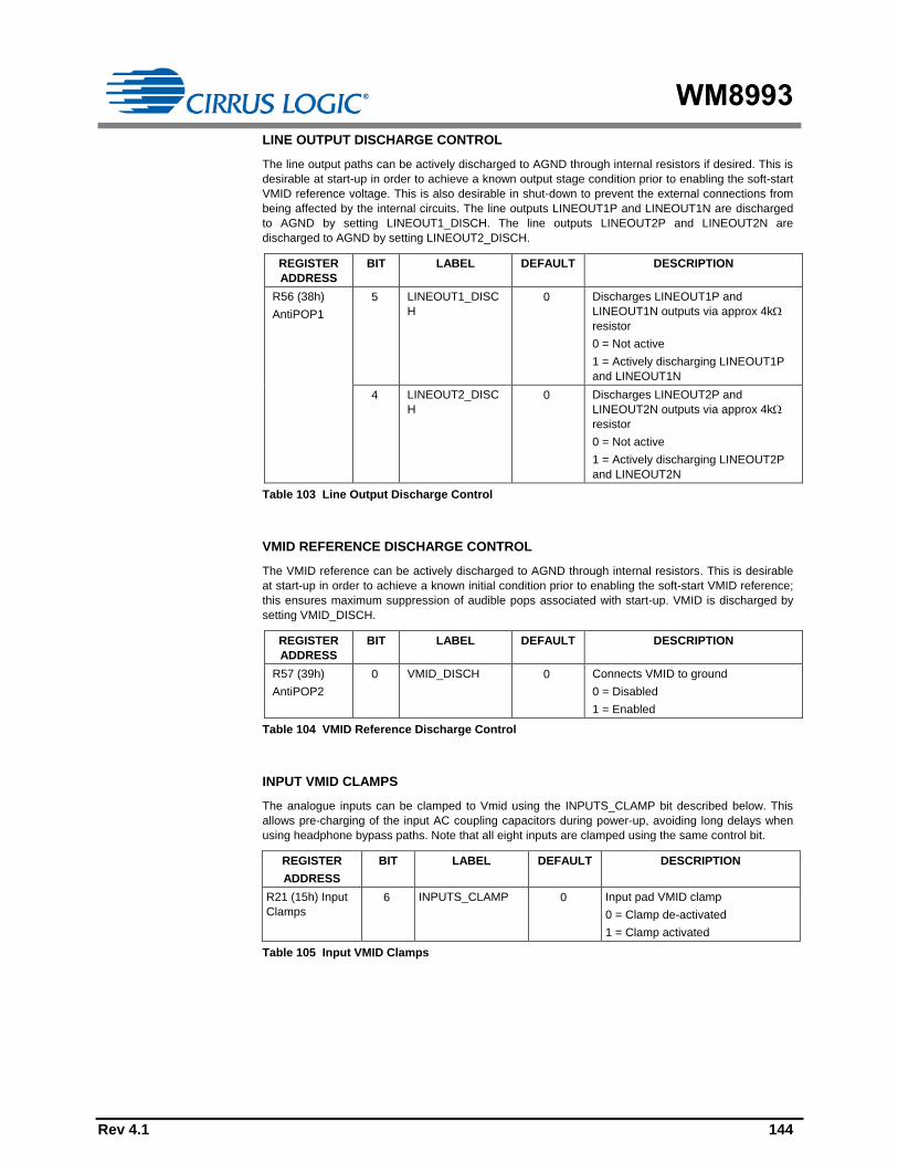
WM8993
Rev 4.1 144
LINE OUTPUT DISCHARGE CONTROL
The line output paths can be actively discharged to AGND through internal resistors if desired. This is
desirable at start-up in order to achieve a known output stage condition prior to enabling the soft-start
VMID reference voltage. This is also desirable in shut-down to prevent the external connections from
being affected by the internal circuits. The line outputs LINEOUT1P and LINEOUT1N are discharged
to AGND by setting LINEOUT1_DISCH. The line outputs LINEOUT2P and LINEOUT2N are
discharged to AGND by setting LINEOUT2_DISCH.
REGISTER
ADDRESS
BIT LABEL DEFAULT DESCRIPTION
R56 (38h)
AntiPOP1
5 LINEOUT1_DISC
H
0 Discharges LINEOUT1P and
LINEOUT1N outputs via approx 4k
resistor
0 = Not active
1 = Actively discharging LINEOUT1P
and LINEOUT1N
4 LINEOUT2_DISC
H
0 Discharges LINEOUT2P and
LINEOUT2N outputs via approx 4k
resistor
0 = Not active
1 = Actively discharging LINEOUT2P
and LINEOUT2N
Table 103 Line Output Discharge Control
VMID REFERENCE DISCHARGE CONTROL
The VMID reference can be actively discharged to AGND through internal resistors. This is desirable
at start-up in order to achieve a known initial condition prior to enabling the soft-start VMID reference;
this ensures maximum suppression of audible pops associated with start-up. VMID is discharged by
setting VMID_DISCH.
REGISTER
ADDRESS
BIT LABEL DEFAULT DESCRIPTION
R57 (39h)
AntiPOP2
0 VMID_DISCH 0 Connects VMID to ground
0 = Disabled
1 = Enabled
Table 104 VMID Reference Discharge Control
INPUT VMID CLAMPS
The analogue inputs can be clamped to Vmid using the INPUTS_CLAMP bit described below. This
allows pre-charging of the input AC coupling capacitors during power-up, avoiding long delays when
using headphone bypass paths. Note that all eight inputs are clamped using the same control bit.
REGISTER
ADDRESS
BIT LABEL DEFAULT DESCRIPTION
R21 (15h) Input
Clamps
6 INPUTS_CLAMP 0 Input pad VMID clamp
0 = Clamp de-activated
1 = Clamp activated
Table 105 Input VMID Clamps
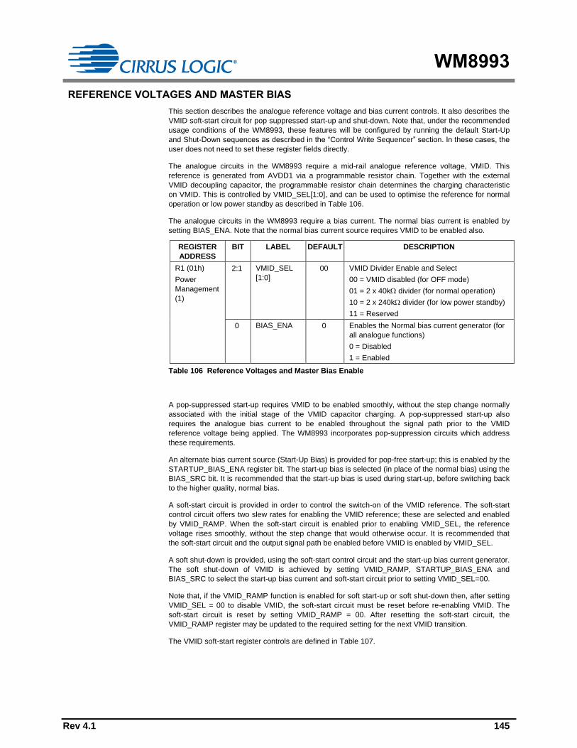
WM8993
Rev 4.1 145
REFERENCE VOLTAGES AND MASTER BIAS
This section describes the analogue reference voltage and bias current controls. It also describes the
VMID soft-start circuit for pop suppressed start-up and shut-down. Note that, under the recommended
usage conditions of the WM8993, these features will be configured by running the default Start-Up
and Shut-Down sequences as described in the “Control Write Sequencer” section. In these cases, the
user does not need to set these register fields directly.
The analogue circuits in the WM8993 require a mid-rail analogue reference voltage, VMID. This
reference is generated from AVDD1 via a programmable resistor chain. Together with the external
VMID decoupling capacitor, the programmable resistor chain determines the charging characteristic
on VMID. This is controlled by VMID_SEL[1:0], and can be used to optimise the reference for normal
operation or low power standby as described in Table 106.
The analogue circuits in the WM8993 require a bias current. The normal bias current is enabled by
setting BIAS_ENA. Note that the normal bias current source requires VMID to be enabled also.
REGISTER
ADDRESS
BIT LABEL DEFAULT DESCRIPTION
R1 (01h)
Power
Management
(1)
2:1 VMID_SEL
[1:0]
00 VMID Divider Enable and Select
00 = VMID disabled (for OFF mode)
01 = 2 x 40k divider (for normal operation)
10 = 2 x 240k divider (for low power standby)
11 = Reserved
0 BIAS_ENA 0 Enables the Normal bias current generator (for
all analogue functions)
0 = Disabled
1 = Enabled
Table 106 Reference Voltages and Master Bias Enable
A pop-suppressed start-up requires VMID to be enabled smoothly, without the step change normally
associated with the initial stage of the VMID capacitor charging. A pop-suppressed start-up also
requires the analogue bias current to be enabled throughout the signal path prior to the VMID
reference voltage being applied. The WM8993 incorporates pop-suppression circuits which address
these requirements.
An alternate bias current source (Start-Up Bias) is provided for pop-free start-up; this is enabled by the
STARTUP_BIAS_ENA register bit. The start-up bias is selected (in place of the normal bias) using the
BIAS_SRC bit. It is recommended that the start-up bias is used during start-up, before switching back
to the higher quality, normal bias.
A soft-start circuit is provided in order to control the switch-on of the VMID reference. The soft-start
control circuit offers two slew rates for enabling the VMID reference; these are selected and enabled
by VMID_RAMP. When the soft-start circuit is enabled prior to enabling VMID_SEL, the reference
voltage rises smoothly, without the step change that would otherwise occur. It is recommended that
the soft-start circuit and the output signal path be enabled before VMID is enabled by VMID_SEL.
A soft shut-down is provided, using the soft-start control circuit and the start-up bias current generator.
The soft shut-down of VMID is achieved by setting VMID_RAMP, STARTUP_BIAS_ENA and
BIAS_SRC to select the start-up bias current and soft-start circuit prior to setting VMID_SEL=00.
Note that, if the VMID_RAMP function is enabled for soft start-up or soft shut-down then, after setting
VMID_SEL = 00 to disable VMID, the soft-start circuit must be reset before re-enabling VMID. The
soft-start circuit is reset by setting VMID_RAMP = 00. After resetting the soft-start circuit, the
VMID_RAMP register may be updated to the required setting for the next VMID transition.
The VMID soft-start register controls are defined in Table 107.

WM8993
Rev 4.1 146
REGISTER
ADDRESS
BIT LABEL DEFAULT DESCRIPTION
R57 (39h)
AntiPOP2
6:5 VMID_RAMP [1:0] 10 VMID soft start enable / slew rate
control
00 = Normal / Slow start
01 = Normal / Fast start
10 = Soft / Slow start
11 = Soft / Fast start
If VMID_RAMP = 1X is selected for
VMID start-up or shut-down, then the
soft-start circuit must be reset by
setting VMID_RAMP=00 after VMID is
disabled, before VMID is re-enabled.
VMID is disabled / enabled using the
VMID_SEL register.
2 STARTUP_BIAS_
ENA
0 Enables the Start-Up bias current
generator
0 = Disabled
1 = Enabled
1 BIAS_SRC 1 Selects the bias current source
0 = Normal bias
1 = Start-Up bias
Table 107 Soft Start Control
POWER MANAGEMENT
The WM8993 has four control registers that allow users to select which functions are active. For
minimum power consumption, unused functions should be disabled. To minimise pop or click noise, it
is important to enable or disable functions in the correct order. See “Control Write Sequencer” for
further details of recommended control sequences.
REGISTER
ADDRESS
BIT LABEL DEFAULT DESCRIPTION
R1 (1h)
Power
Management
(1)
13 SPKOUTR_ENA 0B SPKMIXR Mixer, SPKRVOL PGA and
SPKOUTR Output Enable
0 = Disabled
1 = Enabled
12 SPKOUTL_ENA 0b SPKMIXL Mixer, SPKLVOL PGA and
SPKOUTL Output Enable
0 = Disabled
1 = Enabled
11 HPOUT2_ENA 0b HPOUT2 and HPOUT2MIX Enable
0 = Disabled
1 = Enabled
9 HPOUT1L_ENA 0b Enables HPOUT1L input stage
0 = Disabled
1 = Enabled
For normal operation, this bit should be
set as the first step of the HPOUT1L
Enable sequence.
Note: When HPOUT1_AUTO_PU is set,
the HPOUT1L_ENA bit automatically
enables all stages of the left headphone
driver

WM8993
Rev 4.1 147
REGISTER
ADDRESS
BIT LABEL DEFAULT DESCRIPTION
8 HPOUT1R_ENA 0b Enables HPOUT1R input stage
0 = Disabled
1 = Enabled
For normal operation, this bit should be
set as the first step of the HPOUT1R
Enable sequence.
Note: When HPOUT1_AUTO_PU is set,
the HPOUT1R_ENA bit automatically
enables all stages of the right headphone
driver
5 MICB2_ENA 0b Microphone Bias 2 Enable
0 = OFF (high impedance output)
1 = ON
4 MICB1_ENA 0b Microphone Bias 1 Enable
0 = OFF (high impedance output)
1 = ON
2:1 VMID_SEL
[1:0]
00b VMID Divider Enable and Select
00 = VMID disabled (for OFF mode)
01 = 2 x 40k divider (Normal mode)
10 = 2 x 240k divider (Standby mode)
11 = Reserved
0 BIAS_ENA 0b Enables the Normal bias current
generator (for all analogue functions)
0 = Disabled
1 = Enabled
R2 (02h)
Power
Management
(2)
14 TSHUT_ENA 0b Thermal Sensor Enable
0 = Disabled
1 = Enabled
13 TSHUT_OPDIS 1b Thermal Shutdown Control
(Causes audio outputs to be disabled if
an over-temperature occurs. The thermal
sensor must also be enabled.)
0 = Disabled
1 = Enabled
11 OPCLK_ENA 0b GPIO Clock Output Enable
0 = Disabled
1 = Enabled
9 MIXINL_ENA 0b Left Input Mixer Enable
(Enables MIXINL and RXVOICE input to
MIXINL)
0 = Disabled
1 = Enabled
8 MIXINR_ENA 0b Right Input Mixer Enable
(Enables MIXINR and RXVOICE input to
MIXINR)
0 = Disabled
1 = Enabled
7 IN2L_ENA 0b IN2L Input PGA Enable
0 = Disabled
1 = Enabled
6 IN1L_ENA 0b IN1L Input PGA Enable
0 = Disabled
1 = Enabled

WM8993
Rev 4.1 148
REGISTER
ADDRESS
BIT LABEL DEFAULT DESCRIPTION
5 IN2R_ENA 0b IN2R Input PGA Enable
0 = Disabled
1 = Enabled
4 IN1R_ENA 0b IN1R Input PGA Enable
0 = Disabled
1 = Enabled
1 ADCL_ENA 0b Left ADC Enable
0 = ADC disabled
1 = ADC enabled
0 ADCR_ENA 0b Right ADC Enable
0 = ADC disabled
1 = ADC enabled
R3 (03h)
Power
Management
(3)
13 LINEOUT1N_ENA 0b LINEOUT1N Line Out and
LINEOUT1NMIX Enable
0 = Disabled
1 = Enabled
12 LINEOUT1P_ENA 0b LINEOUT1P Line Out and
LINEOUT1PMIX Enable
0 = Disabled
1 = Enabled
11 LINEOUT2N_ENA 0b LINEOUT2N Line Out and
LINEOUT2NMIX Enable
0 = Disabled
1 = Enabled
10 LINEOUT2P_ENA 0b LINEOUT2P Line Out and
LINEOUT2PMIX Enable
0 = Disabled
1 = Enabled
9 SPKRVOL_ENA 0b SPKMIXR Mixer and SPKRVOL PGA
Enable
0 = Disabled
1 = Enabled
Note that SPKMIXR and SPKRVOL are
also enabled when SPKOUTR_ENA is
set.
8 SPKLVOL_ENA 0b SPKMIXL Mixer and SPKLVOL PGA
Enable
0 = Disabled
1 = Enabled
Note that SPKMIXL and SPKLVOL are
also enabled when SPKOUTL_ENA is
set.
7 MIXOUTLVOL_E
NA
0b MIXOUTL Left Volume Control Enable
0 = Disabled
1 = Enabled
6 MIXOUTRVOL_E
NA
0b MIXOUTR Right Volume Control Enable
0 = Disabled
1 = Enabled
5 MIXOUTL_ENA 0b MIXOUTL Left Output Mixer Enable
0 = Disabled
1 = Enabled
4 MIXOUTR_ENA 0b MIXOUTR Right Output Mixer Enable
0 = Disabled
1 = Enabled
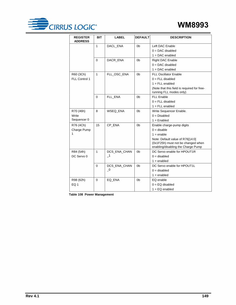
WM8993
Rev 4.1 149
REGISTER
ADDRESS
BIT LABEL DEFAULT DESCRIPTION
1 DACL_ENA 0b Left DAC Enable
0 = DAC disabled
1 = DAC enabled
0 DACR_ENA 0b Right DAC Enable
0 = DAC disabled
1 = DAC enabled
R60 (3Ch)
FLL Control 1
1 FLL_OSC_ENA 0b FLL Oscillator Enable
0 = FLL disabled
1 = FLL enabled
(Note that this field is required for free-
running FLL modes only)
0 FLL_ENA 0b FLL Enable
0 = FLL disabled
1 = FLL enabled
R70 (46h)
Write
Sequencer 0
8 WSEQ_ENA 0b Write Sequencer Enable.
0 = Disabled
1 = Enabled
R76 (4Ch)
Charge Pump
1
15 CP_ENA 0b Enable charge-pump digits
0 = disable
1 = enable
Note: Default value of R76[14:0]
(0x1F25h) must not be changed when
enabling/disabling the Charge Pump
R84 (54h)
DC Servo 0
1 DCS_ENA_CHAN
_1
0b DC Servo enable for HPOUT1R
0 = disabled
1 = enabled
0 DCS_ENA_CHAN
_0
0b DC Servo enable for HPOUT1L
0 = disabled
1 = enabled
R98 (62h)
EQ 1
0 EQ_ENA 0b EQ enable
0 = EQ disabled
1 = EQ enabled
Table 108 Power Management
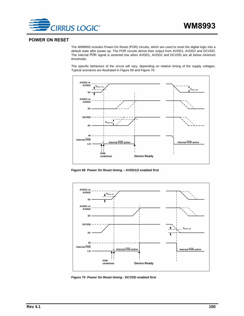
WM8993
Rev 4.1 150
POWER ON RESET
The WM8993 includes Power-On Reset (POR) circuits, which are used to reset the digital logic into a
default state after power up. The POR circuits derive their output from AVDD1, AVDD2 and DCVDD.
The internal POR¯¯¯ signal is asserted low when AVDD1, AVDD2 and DCVDD are all below minimum
thresholds.
The specific behaviour of the circuit will vary, depending on relative timing of the supply voltages.
Typical scenarios are illustrated in Figure 69 and Figure 70.
DCVDD
Vpord_on
0V
0V
AVDD1 or
AVDD2
0V
Vpora_on
Vpora_off
AVDD1 or
AVDD2
LO
POR
Undefined
HI
Internal PORInternal POR active Internal POR active
Device Ready
Figure 69 Power On Reset timing – AVDD1/2 enabled first
DCVDD
0V
0V
AVDD1 or
AVDD2
0V
Vpora_on
Vpord_off
AVDD1 or
AVDD2
LO
POR
Undefined
HI
Internal PORInternal POR active
Device Ready
Internal POR active
Figure 70 Power On Reset timing - DCVDD enabled first

WM8993
Rev 4.1 151
The POR¯¯¯ signal is undefined until AVDD1 or AVDD2 has exceeded the minimum threshold, Vpora_on
Once this threshold has been exceeded, POR¯¯¯ is asserted low and the chip is held in reset. In this
condition, all writes to the control interface are ignored. Once AVDD1, AVDD2 and DCVDD have all
reached their respective power on thresholds, POR¯¯¯ is released high, all registers are in their default
state, and writes to the control interface may take place.
Note that a minimum power-on reset period, TPOR, applies even if AVDD1, AVDD2 and DCVDD have
zero rise time. (This specification is guaranteed by design rather than test.)
On power down, POR¯¯¯ is asserted low when any of AVDD1, AVDD2 or DCVDD falls below their
respective power-down thresholds.
Typical Power-On Reset parameters for the WM8993 are defined in Table 109.
SYMBOL DESCRIPTION MIN TYP MAX UNIT
Vpora_on Power-On threshold (AVDD1 or AVDD2) 1.52 V
Vpora_off Power-Off threshold (AVDD1 or AVDD2) 1.5 V
Vpord_on Power-On threshold (DCVDD) 0.92 V
Vpord_off Power-Off threshold (DCVDD) 0.9 V
TPOR Minimum Power-On Reset period 100 ns
Table 109 Typical Power-On Reset parameters

WM8993
Rev 4.1 152
QUICK START-UP AND SHUTDOWN
The default control sequences (see “Control Write Sequencer”) contain only the register writes
necessary to enable or disable specific output drivers. It is therefore necessary to configure the signal
path and gain settings before commanding any of the default start-up sequences.
This section describes minimum control sequences to configure the WM8993 for DAC to Headphone
playback. Note that these sequences are provided for guidance only; application software should be
verified and tailored to ensure optimum performance.
Table 110 describes an example control sequence to enable the direct DAC to Headphone path. This
involves DAC enable, signal path configuration and mute control, together with the default
“Headphone Cold Start-Up” sequence. Table 111 describes an example control sequence to disable
the direct DAC to Headphone path. Note that these sequences are provided for guidance only;
Application software should be verified and tailored to ensure optimum performance.
REGISTER VALUE DESCRIPTION
R3 (03h) 0003h Enable DACL and DACR
R45 (2Dh) 0100h Enable path from DACL to HPOUT1L
R46 (2Eh) 0100h Enable path from DACR to HPOUT1R
R73 (49h) 0100h Initiate Control Write Sequencer at Index Address 0
(Headphone ‘cold’ Start-Up)
Delay 300ms
Note: Delay must inserted in the sequence to allow the Control
Write Sequencer to finish. Any control interface writes to the
CODEC will be ignored while the Control Write Sequencer is
running.
R10 (0Ah) 0000h Soft un-mute DAC
Table 110 DAC to Headphone Direct Start-Up Sequence
REGISTER VALUE DESCRIPTION
R10 (0Ah) 0004h Soft mute DAC
R73 (49h) 012Ah Initiate Control Write Sequencer at Index Address 42 (Generic
Shut-Down)
Delay 525ms
Note: Delay must inserted in the sequence to allow the Control
Write Sequencer to finish. Any control interface writes to the
CODEC will be ignored while the Control Write Sequencer is
running.
R45 (2Dh) 0000h Disable path from DACL to HPOUT1L
R46 (2Eh) 0000h Disable path from DACR to HPOUT1R
R3 (03h) 0000h Disable DACL and DACR
Table 111 DAC to Headphone Direct Shut-Down Sequence
In both cases, the WSEQ_BUSY bit (in Register R74, see Table 93) will be set to 1 while the Control
Write Sequence runs. When this bit returns to 0, the remaining steps of the sequence may be
executed. Note that it is also possible to use GPIO or Interrupt functions to confirm the status of the
Control Write Sequencer - see “General Purpose Input/Output”.

WM8993
Rev 4.1 153
SOFTWARE RESET AND DEVICE ID
The device ID can be read back from register 0. Writing to this register will reset the device.
The software reset causes most control registers to be reset to their default state. Note that the
Control Write Sequencer registers R12288 (3000h) through to R12799 (31FFh) are not affected by a
software reset; the Control Sequences defined in these registers are retained unchanged.
REGISTER
ADDRESS
BIT LABEL DEFAULT DESCRIPTION
R0 (00h)
Software
Reset
15:0 SW_RESET
[15:0]
8993h Writing to this register resets all registers
to their default state. (Note - Control
Write Sequencer registers are not
affected by Software Reset.)
Reading from this register will indicate
device family ID 8993h.
Table 112 Chip Reset and ID
THERMAL SHUTDOWN
The WM8993 incorporates a temperature sensor which detects when the device temperature is within
normal limits or if the device is approaching a hazardous temperature condition. The Temp OK flag
can be polled at any time, or output directly on the GPIO1 pin, or may be used to generate Interrupt
events.
The temperature sensor can be configured to automatically disable the audio outputs of the WM8993
in response to an overtemperature condition (approximately 150ºC).
The temperature sensor is enabled by setting the TSHUT_ENA register bit. When the TSHUT_OPDIS
is also set, then a device over-temperature condition will cause the speaker outputs (SPKOUTL and
SPKOUTR) of the WM8993 to be disabled; this response is likely to prevent any damage to the device
attributable to the large currents of the output drivers.
Note that, to prevent pops and clicks, TSHUT_ENA and TSHUT_OPDIS should only be updated
whilst the speaker and headphone outputs are disabled.
REGISTER
ADDRESS
BIT LABEL DEFAULT DESCRIPTION
R2 (02h)
Power
Management
(2)
14 TSHUT_ENA 1b Thermal sensor enable
0 = disabled
1 = enabled
13 TSHUT_OPDIS 1b Thermal shutdown control
(Causes audio outputs to be disabled
if an overtemperature occurs. The
thermal sensor must also be enabled.)
0 = disabled
1 = enabled
Table 113 Thermal Shutdown
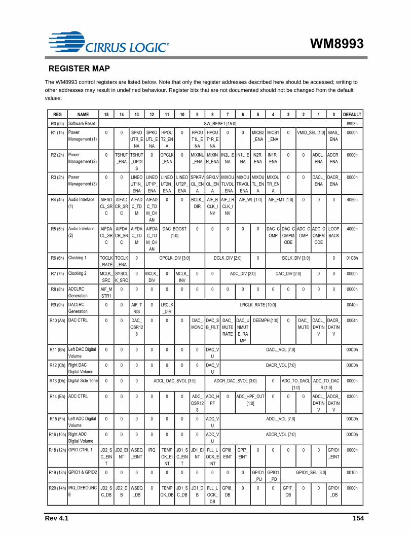
WM8993
Rev 4.1 154
REGISTER MAP
The WM8993 control registers are listed below. Note that only the register addresses described here should be accessed; writing to
other addresses may result in undefined behaviour. Register bits that are not documented should not be changed from the default
values.
REG NAME 15 14 13 12 11 10 9 8 7 6 5 4 3 2 1 0 DEFAULT
R0 (0h) Software Reset SW_RESET [15:0] 8993h
R1 (1h) Power
Management (1)
0 0 SPKO
UTR_E
NA
SPKO
UTL_E
NA
HPOU
T2_EN
A
0 HPOU
T1L_E
NA
HPOU
T1R_E
NA
0 0 MICB2
_ENA
MICB1
_ENA
0 VMID_SEL [1:0] BIAS_
ENA
0000h
R2 (2h) Power
Management (2)
0 TSHUT
_ENA
TSHUT
_OPDI
S
0 OPCLK
_ENA
0 MIXINL
_ENA
MIXIN
R_ENA
IN2L_E
NA
IN1L_E
NA
IN2R_
ENA
IN1R_
ENA
0 0 ADCL_
ENA
ADCR_
ENA
6000h
R3 (3h) Power
Management (3)
0 0 LINEO
UT1N_
ENA
LINEO
UT1P_
ENA
LINEO
UT2N_
ENA
LINEO
UT2P_
ENA
SPKRV
OL_EN
A
SPKLV
OL_EN
A
MIXOU
TLVOL
_ENA
MIXOU
TRVOL
_ENA
MIXOU
TL_EN
A
MIXOU
TR_EN
A
0 0 DACL_
ENA
DACR_
ENA
0000h
R4 (4h) Audio Interface
(1)
AIFAD
CL_SR
C
AIFAD
CR_SR
C
AIFAD
C_TD
M
AIFAD
C_TD
M_CH
AN
0 0 BCLK_
DIR
AIF_B
CLK_I
NV
AIF_LR
CLK_I
NV
AIF_WL [1:0] AIF_FMT [1:0] 0 0 0 4050h
R5 (5h) Audio Interface
(2)
AIFDA
CL_SR
C
AIFDA
CR_SR
C
AIFDA
C_TD
M
AIFDA
C_TD
M_CH
AN
DAC_BOOST
[1:0]
0 0 0 0 0 DAC_C
OMP
DAC_C
OMPM
ODE
ADC_C
OMP
ADC_C
OMPM
ODE
LOOP
BACK
4000h
R6 (6h) Clocking 1 TOCLK
_RATE
TOCLK
_ENA
0 OPCLK_DIV [3:0] DCLK_DIV [2:0] 0 BCLK_DIV [3:0] 0 01C8h
R7 (7h) Clocking 2 MCLK_
SRC
SYSCL
K_SRC
0 MCLK_
DIV
0 MCLK_
INV
0 0 ADC_DIV [2:0] DAC_DIV [2:0] 0 0 0000h
R8 (8h) ADCLRC
Generation
AIF_M
STR1
0 0 0 0 0 0 0 0 0 0 0 0 0 0 0 0000h
R9 (9h) DACLRC
Generation
0 0 AIF_T
RIS
0 LRCLK
_DIR
LRCLK_RATE [10:0] 0040h
R10 (Ah) DAC CTRL 0 0 DAC_
OSR12
8
0 0 0 DAC_
MONO
DAC_S
B_FILT
DAC_
MUTE
RATE
DAC_U
NMUT
E_RA
MP
DEEMPH [1:0] 0 DAC_
MUTE
DACL_
DATIN
V
DACR_
DATIN
V
0004h
R11 (Bh) Left DAC Digital
Volume
0 0 0 0 0 0 0 DAC_V
U
DACL_VOL [7:0] 00C0h
R12 (Ch) Right DAC
Digital Volume
0 0 0 0 0 0 0 DAC_V
U
DACR_VOL [7:0] 00C0h
R13 (Dh) Digital Side Tone 0 0 0 ADCL_DAC_SVOL [3:0] ADCR_DAC_SVOL [3:0] 0 ADC_TO_DACL
[1:0]
ADC_TO_DAC
R [1:0]
0000h
R14 (Eh) ADC CTRL 0 0 0 0 0 0 ADC_
OSR12
8
ADC_H
PF
0 ADC_HPF_CUT
[1:0]
0 0 0 ADCL_
DATIN
V
ADCR_
DATIN
V
0300h
R15 (Fh) Left ADC Digital
Volume
0 0 0 0 0 0 0 ADC_V
U
ADCL_VOL [7:0] 00C0h
R16 (10h) Right ADC
Digital Volume
0 0 0 0 0 0 0 ADC_V
U
ADCR_VOL [7:0] 00C0h
R18 (12h) GPIO CTRL 1 JD2_S
C_EIN
T
JD2_EI
NT
WSEQ
_EINT
IRQ TEMP
OK_EI
NT
JD1_S
C_EIN
T
JD1_EI
NT
FLL_L
OCK_E
INT
GPI8_
EINT
GPI7_
EINT
0 0 0 0 0 GPIO1
_EINT
0000h
R19 (13h) GPIO1 & GPIO2 0 0 0 0 0 0 0 0 0 0 GPIO1
_PU
GPIO1
_PD
GPIO1_SEL [3:0] 0010h
R20 (14h) IRQ_DEBOUNC
E
JD2_S
C_DB
JD2_D
B
WSEQ
_DB
0 TEMP
OK_DB
JD1_S
C_DB
JD1_D
B
FLL_L
OCK_
DB
GPI8_
DB
0 0 0 GPI7_
DB
0 0 GPIO1
_DB
0000h

WM8993
Rev 4.1 155
REG NAME 15 14 13 12 11 10 9 8 7 6 5 4 3 2 1 0 DEFAULT
R21 (15h) Input Mixer1 0 0 0 0 0 0 0 0 0 INPUT
S_CLA
MP
0 0 0 0 0 0 0000h
R22 (16h) GPIOCTRL 2 1 0 IM_JD
2_EINT
IM_JD
2_SC_
EINT
IM_TE
MPOK
_EINT
IM_JD
1_SC_
EINT
IM_JD
1_EINT
IM_FLL
_LOCK
_EINT
0 IM_GPI
8_EINT
IM_GPI
O1_EI
NT
GPI8_
ENA
0 IM_GPI
7_EINT
IM_WS
EQ_EI
NT
GPI7_
ENA
8000h
R23 (17h) GPIO_POL JD2_S
C_POL
JD2_P
OL
WSEQ
_POL
IRQ_P
OL
TEMP
OK_P
OL
JD1_S
C_POL
JD1_P
OL
FLL_L
OCK_P
OL
GPI8_
POL
GPI7_
POL
0 0 0 0 0 GPIO1
_POL
0800h
R24 (18h) Left Line Input
1&2 Volume
0 0 0 0 0 0 0 IN1_V
U
IN1L_
MUTE
IN1L_Z
C
0 IN1L_VOL [4:0] 008Bh
R25 (19h) Left Line Input
3&4 Volume
0 0 0 0 0 0 0 IN2_V
U
IN2L_
MUTE
IN2L_Z
C
0 IN2L_VOL [4:0] 008Bh
R26 (1Ah) Right Line Input
1&2 Volume
0 0 0 0 0 0 0 IN1_V
U
IN1R_
MUTE
IN1R_
ZC
0 IN1R_VOL [4:0] 008Bh
R27 (1Bh) Right Line Input
3&4 Volume
0 0 0 0 0 0 0 IN2_V
U
IN2R_
MUTE
IN2R_
ZC
0 IN2R_VOL [4:0] 008Bh
R28 (1Ch) Left Output
Volume
0 0 0 0 0 0 0 HPOU
T1_VU
HPOU
T1L_Z
C
HPOU
T1L_M
UTE_N
HPOUT1L_VOL [5:0] 006Dh
R29 (1Dh) Right Output
Volume
0 0 0 0 0 0 0 HPOU
T1_VU
HPOU
T1R_Z
C
HPOU
T1R_M
UTE_N
HPOUT1R_VOL [5:0] 006Dh
R30 (1Eh) Line Outputs
Volume
0 0 0 0 0 0 0 0 0 LINEO
UT1N_
MUTE
LINEO
UT1P_
MUTE
LINEO
UT1_V
OL
0 LINEO
UT2N_
MUTE
LINEO
UT2P_
MUTE
LINEO
UT2_V
OL
0066h
R31 (1Fh) HPOUT2
Volume
0 0 0 0 0 0 0 0 0 0 HPOU
T2_MU
TE
HPOU
T2_VO
L
0 0 0 0 0020h
R32 (20h) Left OPGA
Volume
0 0 0 0 0 0 0 MIXOU
T_VU
MIXOU
TL_ZC
MIXOU
TL_MU
TE_N
MIXOUTL_VOL [5:0] 0079h
R33 (21h) Right OPGA
Volume
0 0 0 0 0 0 0 MIXOU
T_VU
MIXOU
TR_ZC
MIXOU
TR_M
UTE_N
MIXOUTR_VOL [5:0] 0079h
R34 (22h) SPKMIXL
Attenuation
0 0 0 0 0 0 0 0 0 0 MIXINL
_SPKM
IXL_V
OL
IN1LP_
SPKMI
XL_VO
L
MIXOU
TL_SP
KMIXL
_VOL
DACL_
SPKMI
XL_VO
L
SPKMIXL_VOL
[1:0]
0003h
R35 (23h) SPKMIXR
Attenuation
0 0 0 0 0 0 0 SPKO
UT_CL
ASSAB
_MOD
E
0 0 MIXIN
R_SPK
MIXR_
VOL
IN1RP
_SPKM
IXR_V
OL
MIXOU
TR_SP
KMIXR
_VOL
DACR_
SPKMI
XR_VO
L
SPKMIXR_VOL
[1:0]
0003h
R36 (24h) SPKOUT Mixers 0 0 0 0 0 0 0 0 0 0 IN2LP_
TO_SP
KOUTL
SPKMI
XL_TO
_SPKO
UTL
SPKMI
XR_TO
_SPKO
UTL
IN2LP_
TO_SP
KOUT
R
SPKMI
XL_TO
_SPKO
UTR
SPKMI
XR_TO
_SPKO
UTR
0011h
R37 (25h) ClassD3 0 0 0 0 0 0 0 0 0 0 SPKOUTL_BOOST [2:0] SPKOUTR_BOOST [2:0] 0000h
R38 (26h) Speaker Volume
Left
0 0 0 0 0 0 0 SPKO
UT_VU
SPKO
UTL_Z
C
SPKO
UTL_M
UTE_N
SPKOUTL_VOL [5:0] 0079h
R39 (27h) Speaker Volume
Right
0 0 0 0 0 0 0 SPKO
UT_VU
SPKO
UTR_Z
C
SPKO
UTR_
MUTE_
N
SPKOUTR_VOL [5:0] 0079h
R40 (28h) Input Mixer2 0 0 0 0 0 0 0 0 IN2LP_
TO_IN
2L
IN2LN_
TO_IN
2L
IN1LP_
TO_IN
1L
IN1LN_
TO_IN
1L
IN2RP
_TO_I
N2R
IN2RN
_TO_I
N2R
IN1RP
_TO_I
N1R
IN1RN
_TO_I
N1R
0000h

WM8993
Rev 4.1 156
REG NAME 15 14 13 12 11 10 9 8 7 6 5 4 3 2 1 0 DEFAULT
R41 (29h) Input Mixer3 0 0 0 0 0 0 0 IN2L_T
O_MIXI
NL
IN2L_
MIXINL
_VOL
0 IN1L_T
O_MIXI
NL
IN1L_
MIXINL
_VOL
0 MIXOUTL_MIXINL_VOL
[2:0]
0000h
R42 (2Ah) Input Mixer4 0 0 0 0 0 0 0 IN2R_
TO_MI
XINR
IN2R_
MIXIN
R_VOL
0 IN1R_
TO_MI
XINR
IN1R_
MIXIN
R_VOL
0 MIXOUTR_MIXINR_VOL
[2:0]
0000h
R43 (2Bh) Input Mixer5 0 0 0 0 0 0 0 IN1LP_MIXINL_VOL
[2:0]
0 0 0 IN2LP_MIXINL_VOL
[2:0]
0000h
R44 (2Ch) Input Mixer6 0 0 0 0 0 0 0 IN1RP_MIXINR_VOL
[2:0]
0 0 0 IN2LP_MIXINR_VOL
[2:0]
0000h
R45 (2Dh) Output Mixer1 0 0 0 0 0 0 0 DACL_
TO_HP
OUT1L
MIXIN
R_TO_
MIXOU
TL
MIXINL
_TO_M
IXOUT
L
IN2RN
_TO_M
IXOUT
L
IN2LN_
TO_MI
XOUTL
IN1R_
TO_MI
XOUTL
IN1L_T
O_MIX
OUTL
IN2LP_
TO_MI
XOUTL
DACL_
TO_MI
XOUTL
0000h
R46 (2Eh) Output Mixer2 0 0 0 0 0 0 0 DACR_
TO_HP
OUT1R
MIXINL
_TO_M
IXOUT
R
MIXIN
R_TO_
MIXOU
TR
IN2LN_
TO_MI
XOUT
R
IN2RN
_TO_M
IXOUT
R
IN1L_T
O_MIX
OUTR
IN1R_
TO_MI
XOUT
R
IN2RP
_TO_M
IXOUT
R
DACR_
TO_MI
XOUT
R
0000h
R47 (2Fh) Output Mixer3 0 0 0 0 IN2LP_MIXOUTL_VOL
[2:0]
IN2LN_MIXOUTL_VOL
[2:0]
IN1R_MIXOUTL_VOL
[2:0]
IN1L_MIXOUTL_VOL
[2:0]
0000h
R48 (30h) Output Mixer4 0 0 0 0 IN2RP_MIXOUTR_VOL
[2:0]
IN2RN_MIXOUTR_VOL
[2:0]
IN1L_MIXOUTR_VOL
[2:0]
IN1R_MIXOUTR_VOL
[2:0]
0000h
R49 (31h) Output Mixer5 0 0 0 0 DACL_MIXOUTL_VOL
[2:0]
IN2RN_MIXOUTL_VOL
[2:0]
MIXINR_MIXOUTL_VOL
[2:0]
MIXINL_MIXOUTL_VOL
[2:0]
0000h
R50 (32h) Output Mixer6 0 0 0 0 DACR_MIXOUTR_VOL
[2:0]
IN2LN_MIXOUTR_VOL
[2:0]
MIXINL_MIXOUTR_VOL
[2:0]
MIXINR_MIXOUTR_VOL
[2:0]
0000h
R51 (33h) HPOUT2 Mixer 0 0 0 0 0 0 0 0 0 0 IN2LR
P_TO_
HPOU
T2
MIXOU
TLVOL
_TO_H
POUT2
MIXOU
TRVOL
_TO_H
POUT2
0 0 0 0000h
R52 (34h) Line Mixer1 0 0 0 0 0 0 0 0 0 MIXOU
TL_TO
_LINE
OUT1N
MIXOU
TR_TO
_LINE
OUT1N
LINEO
UT1_M
ODE
0 IN1R_
TO_LI
NEOU
T1P
IN1L_T
O_LIN
EOUT1
P
MIXOU
TL_TO
_LINE
OUT1P
0000h
R53 (35h) Line Mixer2 0 0 0 0 0 0 0 0 0 MIXOU
TR_TO
_LINE
OUT2N
MIXOU
TL_TO
_LINE
OUT2N
LINEO
UT2_M
ODE
0 IN1L_T
O_LIN
EOUT2
P
IN1R_
TO_LI
NEOU
T2P
MIXOU
TR_TO
_LINE
OUT2P
0000h
R54 (36h) Speaker Mixer 0 0 0 0 0 0 0 SPKAB
_REF_
SEL
MIXINL
_TO_S
PKMIX
L
MIXIN
R_TO_
SPKMI
XR
IN1LP_
TO_SP
KMIXL
IN1RP
_TO_S
PKMIX
R
MIXOU
TL_TO
_SPKM
IXL
MIXOU
TR_TO
_SPKM
IXR
DACL_
TO_SP
KMIXL
DACR_
TO_SP
KMIXR
0000h
R55 (37h) Additional
Control
0 0 0 0 0 0 0 0 LINEO
UT1_F
B
LINEO
UT2_F
B
0 0 0 0 0 VROI 0000h
R56 (38h) AntiPOP1 0 0 0 0 0 0 0 0 LINEO
UT_VM
ID_BU
F_ENA
HPOU
T2_IN_
ENA
LINEO
UT1_D
ISCH
LINEO
UT2_D
ISCH
0 0 0 0 0000h
R57 (39h) AntiPOP2 0 0 0 0 0 0 0 0 0 VMID_RAMP
[1:0]
0 VMID_
BUF_E
NA
START
UP_BI
AS_EN
A
BIAS_
SRC
VMID_
DISCH
0000h
R58 (3Ah) MICBIAS 0 0 0 0 0 0 0 0 JD_SCTHR
[1:0]
JD_THR [2:0] JD_EN
A
MICB2
_LVL
MICB1
_LVL
0000h
R60 (3Ch) FLL Control 1 0 0 0 0 0 0 0 0 0 0 0 0 0 FLL_F
RAC
FLL_O
SC_EN
A
FLL_E
NA
0000h
R61 (3Dh) FLL Control 2 0 0 0 0 0 FLL_OUTDIV [2:0] 0 0 0 0 0 FLL_FRATIO [2:0] 0000h
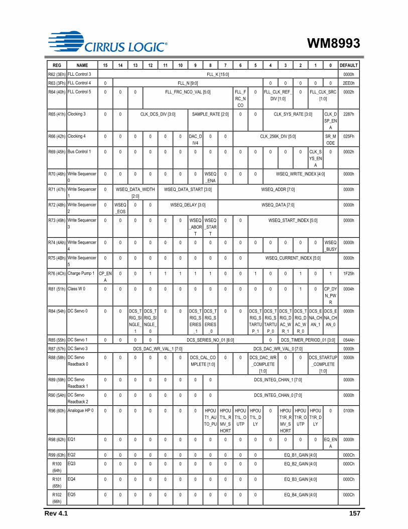
WM8993
Rev 4.1 157
REG NAME 15 14 13 12 11 10 9 8 7 6 5 4 3 2 1 0 DEFAULT
R62 (3Eh) FLL Control 3 FLL_K [15:0] 0000h
R63 (3Fh) FLL Control 4 0 FLL_N [9:0] 0 0 0 0 0 2EE0h
R64 (40h) FLL Control 5 0 0 0 FLL_FRC_NCO_VAL [5:0] FLL_F
RC_N
CO
0 FLL_CLK_REF_
DIV [1:0]
0 FLL_CLK_SRC
[1:0]
0002h
R65 (41h) Clocking 3 0 0 CLK_DCS_DIV [3:0] SAMPLE_RATE [2:0] 0 0 CLK_SYS_RATE [3:0] CLK_D
SP_EN
A
2287h
R66 (42h) Clocking 4 0 0 0 0 0 0 DAC_D
IV4
0 0 CLK_256K_DIV [5:0] SR_M
ODE
025Fh
R69 (45h) Bus Control 1 0 0 0 0 0 0 0 0 0 0 0 0 0 0 CLK_S
YS_EN
A
0 0002h
R70 (46h) Write Sequencer
0
0 0 0 0 0 0 0 WSEQ
_ENA
0 0 0 WSEQ_WRITE_INDEX [4:0] 0000h
R71 (47h) Write Sequencer
1
0 WSEQ_DATA_WIDTH
[2:0]
WSEQ_DATA_START [3:0] WSEQ_ADDR [7:0] 0000h
R72 (48h) Write Sequencer
2
0 WSEQ
_EOS
0 0 WSEQ_DELAY [3:0] WSEQ_DATA [7:0] 0000h
R73 (49h) Write Sequencer
3
0 0 0 0 0 0 WSEQ
_ABOR
T
WSEQ
_STAR
T
0 0 WSEQ_START_INDEX [5:0] 0000h
R74 (4Ah) Write Sequencer
4
0 0 0 0 0 0 0 0 0 0 0 0 0 0 0 WSEQ
_BUSY
0000h
R75 (4Bh) Write Sequencer
5
0 0 0 0 0 0 0 0 0 0 WSEQ_CURRENT_INDEX [5:0] 0000h
R76 (4Ch) Charge Pump 1 CP_EN
A
0 0 1 1 1 1 1 0 0 1 0 0 1 0 1 1F25h
R81 (51h) Class W 0 0 0 0 0 0 0 0 0 0 0 0 0 0 1 0 CP_DY
N_PW
R
0004h
R84 (54h) DC Servo 0 0 0 DCS_T
RIG_SI
NGLE_
1
DCS_T
RIG_SI
NGLE_
0
0 0 DCS_T
RIG_S
ERIES
_1
DCS_T
RIG_S
ERIES
_0
0 0 DCS_T
RIG_S
TARTU
P_1
DCS_T
RIG_S
TARTU
P_0
DCS_T
RIG_D
AC_W
R_1
DCS_T
RIG_D
AC_W
R_0
DCS_E
NA_CH
AN_1
DCS_E
NA_CH
AN_0
0000h
R85 (55h) DC Servo 1 0 0 0 0 DCS_SERIES_NO_01 [6:0] 0 DCS_TIMER_PERIOD_01 [3:0] 054Ah
R87 (57h) DC Servo 3 DCS_DAC_WR_VAL_1 [7:0] DCS_DAC_WR_VAL_0 [7:0] 0000h
R88 (58h) DC Servo
Readback 0
0 0 0 0 0 0 DCS_CAL_CO
MPLETE [1:0]
0 0 DCS_DAC_WR
_COMPLETE
[1:0]
0 0 DCS_STARTUP
_COMPLETE
[1:0]
0000h
R89 (59h) DC Servo
Readback 1
0 0 0 0 0 0 0 0 DCS_INTEG_CHAN_1 [7:0] 0000h
R90 (5Ah) DC Servo
Readback 2
0 0 0 0 0 0 0 0 DCS_INTEG_CHAN_0 [7:0] 0000h
R96 (60h) Analogue HP 0 0 0 0 0 0 0 0 HPOU
T1_AU
TO_PU
HPOU
T1L_R
MV_S
HORT
HPOU
T1L_O
UTP
HPOU
T1L_D
LY
0 HPOU
T1R_R
MV_S
HORT
HPOU
T1R_O
UTP
HPOU
T1R_D
LY
0 0100h
R98 (62h) EQ1 0 0 0 0 0 0 0 0 0 0 0 0 0 0 0 EQ_EN
A
0000h
R99 (63h) EQ2 0 0 0 0 0 0 0 0 0 0 0 EQ_B1_GAIN [4:0] 000Ch
R100
(64h)
EQ3 0 0 0 0 0 0 0 0 0 0 0 EQ_B2_GAIN [4:0] 000Ch
R101
(65h)
EQ4 0 0 0 0 0 0 0 0 0 0 0 EQ_B3_GAIN [4:0] 000Ch
R102
(66h)
EQ5 0 0 0 0 0 0 0 0 0 0 0 EQ_B4_GAIN [4:0] 000Ch

WM8993
Rev 4.1 158
REG NAME 15 14 13 12 11 10 9 8 7 6 5 4 3 2 1 0 DEFAULT
R103
(67h)
EQ6 0 0 0 0 0 0 0 0 0 0 0 EQ_B5_GAIN [4:0] 000Ch
R104
(68h)
EQ7 EQ_B1_A [15:0] 0FCAh
R105
(69h)
EQ8 EQ_B1_B [15:0] 0400h
R106
(6Ah)
EQ9 EQ_B1_PG [15:0] 00D8h
R107
(6Bh)
EQ10 EQ_B2_A [15:0] 1EB5h
R108
(6Ch)
EQ11 EQ_B2_B [15:0] F145h
R109
(6Dh)
EQ12 EQ_B2_C [15:0] 0B75h
R110
(6Eh)
EQ13 EQ_B2_PG [15:0] 01C5h
R111
(6Fh)
EQ14 EQ_B3_A [15:0] 1C58h
R112
(70h)
EQ15 EQ_B3_B [15:0] F373h
R113
(71h)
EQ16 EQ_B3_C [15:0] 0A54h
R114
(72h)
EQ17 EQ_B3_PG [15:0] 0558h
R115
(73h)
EQ18 EQ_B4_A [15:0] 168Eh
R116
(74h)
EQ19 EQ_B4_B [15:0] F829h
R117
(75h)
EQ20 EQ_B4_C [15:0] 07ADh
R118
(76h)
EQ21 EQ_B4_PG [15:0] 1103h
R119
(77h)
EQ22 EQ_B5_A [15:0] 0564h
R120
(78h)
EQ23 EQ_B5_B [15:0] 0559h
R121
(79h)
EQ24 EQ_B5_PG [15:0] 4000h
R122
(7Ah)
Digital Pulls 0 0 0 0 0 0 0 0 MCLK_
PU
MCLK_
PD
DACD
AT_PU
DACD
AT_PD
LRCLK
_PU
LRCLK
_PD
BCLK_
PU
BCLK_
PD
0000h
R123
(7Bh)
DRC Control 1 DRC_E
NA
DRC_D
AC_PA
TH
0 0 DRC_S
MOOT
H_ENA
DRC_
QR_E
NA
DRC_A
NTICLI
P_ENA
DRC_
HYST_
ENA
0 0 DRC_THRESH
_HYST [1:0]
DRC_MINGAIN
[1:0]
DRC_MAXGAIN
[1:0]
0F08h
R124
(7Ch)
DRC Control 2 DRC_ATTACK_RATE [3:0] DRC_DECAY_RATE [3:0] DRC_THRESH_COMP [5:0] 0 0 0000h
R125
(7Dh)
DRC Control 3 DRC_AMP_COMP [4:0] DRC_R0_SLOPE_COM
P [2:0]
DRC_F
F_DEL
AY
0 0 0 DRC_THRESH
_QR [1:0]
DRC_RATE_Q
R [1:0]
0080h
R126
(7Eh)
DRC Control 4 DRC_R1_SLOPE_COM
P [2:0]
DRC_STARTUP_GAIN [4:0] 0 0 0 0 0 0 0 0 0000h

WM8993
Rev 4.1 159
REGISTER BITS BY ADDRESS
REGISTER
ADDRESS
BIT LABEL DEFAULT DESCRIPTION
R0 (00h)
Software
Reset
15:0 SW_RESET
[15:0]
1000_1001
_1001_001
1
Writing to this register resets all registers to their default
state. (Note - Control Write Sequencer registers are not
affected by Software Reset.)
Reading from this register will indicate device family ID
8993h.
Register 00h Software Reset
REGISTER
ADDRESS
BIT LABEL DEFAULT DESCRIPTION
R1 (01h)
Power
Management
(1)
13 SPKOUTR_ENA 0 SPKMIXR Mixer, SPKRVOL PGA and SPKOUTR Output
Enable
0 = Disabled
1 = Enabled
12 SPKOUTL_ENA 0 SPKMIXL Mixer, SPKLVOL PGA and SPKOUTL Output
Enable
0 = Disabled
1 = Enabled
11 HPOUT2_ENA 0 HPOUT2 Output Stage Enable
0 = Disabled
1 = Enabled
9 HPOUT1L_ENA 0 Enables HPOUT1L input stage
0 = Disabled
1 = Enabled
For normal operation, this bit should be set as the first step
of the HPOUT1L Enable sequence.
Note: When HPOUT1_AUTO_PU is set, the
HPOUT1L_ENA bit automatically enables all stages of the
left headphone driver
8 HPOUT1R_ENA 0 Enables HPOUT1R input stage
0 = Disabled
1 = Enabled
For normal operation, this bit should be set as the first step
of the HPOUT1R Enable sequence.
Note: When HPOUT1_AUTO_PU is set, the
HPOUT1R_ENA bit automatically enables all stages of the
right headphone driver
5 MICB2_ENA 0 Microphone Bias 2 Enable
0 = OFF (high impedance output)
1 = ON
4 MICB1_ENA 0 Microphone Bias 1 Enable
0 = OFF (high impedance output)
1 = ON
2:1 VMID_SEL [1:0] 00 VMID Divider Enable and Select
00 = VMID disabled (for OFF mode)
11 = Reserved
0 BIAS_ENA 0 Enables the Normal bias current generator (for all analogue
functions)
0 = Disabled
1 = Enabled

WM8993
Rev 4.1 160
Register 01h Power Management (1)
REGISTER
ADDRESS
BIT LABEL DEFAULT DESCRIPTION
R2 (02h)
Power
Management
(2)
14 TSHUT_ENA 1 Thermal sensor enable
0 = disabled
1 = enabled
13 TSHUT_OPDIS 1 Thermal shutdown control
(Causes audio outputs to be disabled if an overtemperature
occurs. The thermal sensor must also be enabled.)
0 = disabled
1 = enabled
11 OPCLK_ENA 0 GPIO Clock Output Enable
0 = disabled
1 = enabled
9 MIXINL_ENA 0 Left Input Mixer Enable
(Enables MIXINL and RXVOICE input to MIXINL)
0 = Disabled
1 = Enabled
8 MIXINR_ENA 0 Right Input Mixer Enable
(Enables MIXINR and RXVOICE input to MIXINR)
0 = Disabled
1 = Enabled
7 IN2L_ENA 0 IN2L Input PGA Enable
0 = Disabled
1 = Enabled
6 IN1L_ENA 0 IN1L Input PGA Enable
0 = Disabled
1 = Enabled
5 IN2R_ENA 0 IN2R Input PGA Enable
0 = Disabled
1 = Enabled
4 IN1R_ENA 0 IN1R Input PGA Enable
0 = Disabled
1 = Enabled
1 ADCL_ENA 0 Left ADC Enable
0 = ADC disabled
1 = ADC enabled
0 ADCR_ENA 0 Right ADC Enable
0 = ADC disabled
1 = ADC enabled
Register 02h Power Management (2)
REGISTER
ADDRESS
BIT LABEL DEFAULT DESCRIPTION
R3 (03h)
Power
Management
(3)
13 LINEOUT1N_EN
A
0 LINEOUT1N Line Out and LINEOUT1NMIX Enable
0 = Disabled
1 = Enabled
12 LINEOUT1P_EN
A
0 LINEOUT1P Line Out and LINEOUT1PMIX Enable
0 = Disabled
1 = Enabled
11 LINEOUT2N_EN 0 LINEOUT2N Line Out and LINEOUT2NMIX Enable
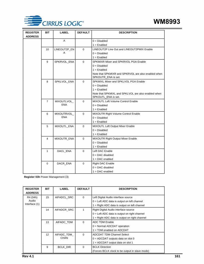
WM8993
Rev 4.1 161
REGISTER
ADDRESS
BIT LABEL DEFAULT DESCRIPTION
A 0 = Disabled
1 = Enabled
10 LINEOUT2P_EN
A
0 LINEOUT2P Line Out and LINEOUT2PMIX Enable
0 = Disabled
1 = Enabled
9 SPKRVOL_ENA 0 SPKMIXR Mixer and SPKRVOL PGA Enable
0 = Disabled
1 = Enabled
Note that SPKMIXR and SPKRVOL are also enabled when
SPKOUTR_ENA is set.
8 SPKLVOL_ENA 0 SPKMIXL Mixer and SPKLVOL PGA Enable
0 = Disabled
1 = Enabled
Note that SPKMIXL and SPKLVOL are also enabled when
SPKOUTL_ENA is set.
7 MIXOUTLVOL_
ENA
0 MIXOUTL Left Volume Control Enable
0 = Disabled
1 = Enabled
6 MIXOUTRVOL_
ENA
0 MIXOUTR Right Volume Control Enable
0 = Disabled
1 = Enabled
5 MIXOUTL_ENA 0 MIXOUTL Left Output Mixer Enable
0 = Disabled
1 = Enabled
4 MIXOUTR_ENA 0 MIXOUTR Right Output Mixer Enable
0 = Disabled
1 = Enabled
1 DACL_ENA 0 Left DAC Enable
0 = DAC disabled
1 = DAC enabled
0 DACR_ENA 0 Right DAC Enable
0 = DAC disabled
1 = DAC enabled
Register 03h Power Management (3)
REGISTER
ADDRESS
BIT LABEL DEFAULT DESCRIPTION
R4 (04h)
Audio
Interface (1)
15 AIFADCL_SRC 0 Left Digital Audio interface source
0 = Left ADC data is output on left channel
1 = Right ADC data is output on left channel
14 AIFADCR_SRC 1 Right Digital Audio interface source
0 = Left ADC data is output on right channel
1 = Right ADC data is output on right channel
13 AIFADC_TDM 0 ADC TDM Enable
0 = Normal ADCDAT operation
1 = TDM enabled on ADCDAT
12 AIFADC_TDM_
CHAN
0 ADCDAT TDM Channel Select
0 = ADCDAT outputs data on slot 0
1 = ADCDAT output data on slot 1
9 BCLK_DIR 0 BCLK Direction
(Forces BCLK clock to be output in slave mode)

WM8993
Rev 4.1 162
REGISTER
ADDRESS
BIT LABEL DEFAULT DESCRIPTION
0 = BCLK normal operation
1 = BCLK clock output enabled
8 AIF_BCLK_INV 0 BCLK Invert
0 = BCLK not inverted
1 = BCLK inverted
Note that AIF_BCLK_INV selects the BCLK polarity in
Master mode and in Slave mode.
7 AIF_LRCLK_IN
V
0 Right, left and I2S modes – LRCLK polarity
0 = normal LRCLK polarity
1 = invert LRCLK polarity
Note that AIF_LRCLK_INV selects the LRCLK polarity in
Master mode and in Slave mode.
DSP Mode – mode A/B select
0 = MSB is available on 2nd BCLK rising edge after LRC
rising edge (mode A)
1 = MSB is available on 1st BCLK rising edge after LRC
rising edge (mode B)
6:5 AIF_WL [1:0] 10 Digital Audio Interface Word Length
00 = 16 bits
01 = 20 bits
10 = 24 bits
11 = 32 bits
4:3 AIF_FMT [1:0] 10 Digital Audio Interface Format
00 = Right justified
01 = Left justified
10 = I2S Format
11 = DSP Mode
Register 04h Audio Interface (1)
REGISTER
ADDRESS
BIT LABEL DEFAULT DESCRIPTION
R5 (05h)
Audio
Interface (2)
15 AIFDACL_SRC 0 Left DAC Data Source Select
0 = Left DAC outputs left interface data
1 = Left DAC outputs right interface data
14 AIFDACR_SRC 1 Right DAC Data Source Select
0 = Right DAC outputs left interface data
1 = Right DAC outputs right interface data
13 AIFDAC_TDM 0 DAC TDM Enable
0 = Normal DACDAT operation
1 = TDM enabled on DACDAT
12 AIFDAC_TDM_
CHAN
0 DACDAT TDM Channel Select
0 = DACDAT data input on slot 0
1 = DACDAT data input on slot 1
11:10 DAC_BOOST
[1:0]
00 DAC Input Volume Boost
00 = 0dB
01 = +6dB (Input data must not exceed -6dBFS)
10 = +12dB (Input data must not exceed -12dBFS)
11 = +18dB (Input data must not exceed -18dBFS)
4 DAC_COMP 0 DAC Companding Enable
0 = disabled

WM8993
Rev 4.1 163
REGISTER
ADDRESS
BIT LABEL DEFAULT DESCRIPTION
1 = enabled
3 DAC_COMPMO
DE
0 DAC Companding Type
0 = µ-law
1 = A-law
2 ADC_COMP 0 ADC Companding Enable
0 = disabled
1 = enabled
1 ADC_COMPMO
DE
0 ADC Companding Type
0 = µ-law
1 = A-law
0 LOOPBACK 0 Digital Loopback Function
0 = No loopback
1 = Loopback enabled (ADC data output is directly input to
DAC data input).
Register 05h Audio Interface (2)
REGISTER
ADDRESS
BIT LABEL DEFAULT DESCRIPTION
R6 (06h)
Clocking 1
15 TOCLK_RATE 0 TOCLK Rate Divider (/2)
0 = f / 2
1 = f / 1
14 TOCLK_ENA 0 TOCLK Enable
0 = disabled
1 = enabled
12:9 OPCLK_DIV
[3:0]
0000 GPIO Output Clock Divider
0000 = CLK_SYS
0001 = CLK_SYS / 2
0010 = CLK_SYS / 3
0011 = CLK_SYS / 4
0100 = CLK_SYS / 5.5
0101 = CLK_SYS / 6
0110 = CLK_SYS / 8
0111 = CLK_SYS / 12
1000 = CLK_SYS / 16
1001 to 1111 = Reserved
8:6 DCLK_DIV [2:0] 111 Class D Clock Divider
000 = CLK_SYS
001 = CLK_SYS / 2
010 = CLK_SYS / 3
011 = CLK_SYS / 4
100 = CLK_SYS / 6
101 = CLK_SYS / 8
110 = CLK_SYS / 12
111 = CLK_SYS / 16
Note - this field is ignored and invalid in Automatic Clocking
Configuration mode.
4:1 BCLK_DIV [3:0] 0100 BCLK Rate
0000 = CLK_SYS
0001 = CLK_SYS / 1.5
0010 = CLK_SYS / 2
0011 = CLK_SYS / 3
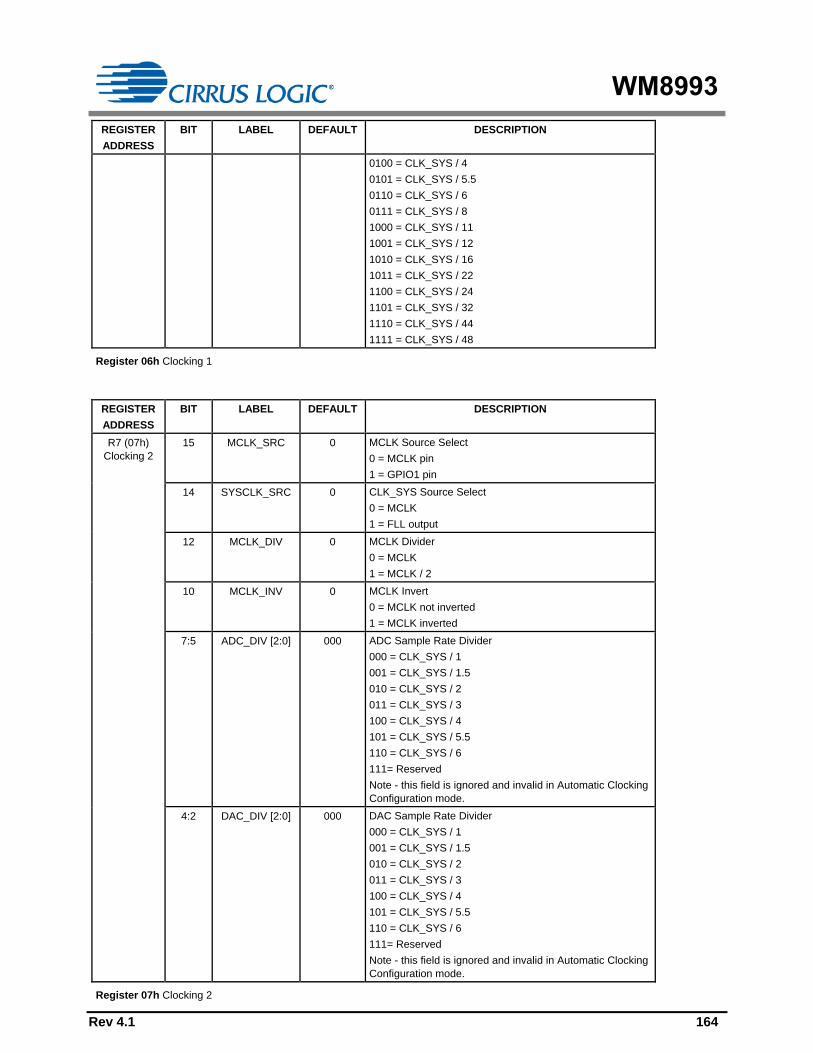
WM8993
Rev 4.1 164
REGISTER
ADDRESS
BIT LABEL DEFAULT DESCRIPTION
0100 = CLK_SYS / 4
0101 = CLK_SYS / 5.5
0110 = CLK_SYS / 6
0111 = CLK_SYS / 8
1000 = CLK_SYS / 11
1001 = CLK_SYS / 12
1010 = CLK_SYS / 16
1011 = CLK_SYS / 22
1100 = CLK_SYS / 24
1101 = CLK_SYS / 32
1110 = CLK_SYS / 44
1111 = CLK_SYS / 48
Register 06h Clocking 1
REGISTER
ADDRESS
BIT LABEL DEFAULT DESCRIPTION
R7 (07h)
Clocking 2
15 MCLK_SRC 0 MCLK Source Select
0 = MCLK pin
1 = GPIO1 pin
14 SYSCLK_SRC 0 CLK_SYS Source Select
0 = MCLK
1 = FLL output
12 MCLK_DIV 0 MCLK Divider
0 = MCLK
1 = MCLK / 2
10 MCLK_INV 0 MCLK Invert
0 = MCLK not inverted
1 = MCLK inverted
7:5 ADC_DIV [2:0] 000 ADC Sample Rate Divider
000 = CLK_SYS / 1
001 = CLK_SYS / 1.5
010 = CLK_SYS / 2
011 = CLK_SYS / 3
100 = CLK_SYS / 4
101 = CLK_SYS / 5.5
110 = CLK_SYS / 6
111= Reserved
Note - this field is ignored and invalid in Automatic Clocking
Configuration mode.
4:2 DAC_DIV [2:0] 000 DAC Sample Rate Divider
000 = CLK_SYS / 1
001 = CLK_SYS / 1.5
010 = CLK_SYS / 2
011 = CLK_SYS / 3
100 = CLK_SYS / 4
101 = CLK_SYS / 5.5
110 = CLK_SYS / 6
111= Reserved
Note - this field is ignored and invalid in Automatic Clocking
Configuration mode.
Register 07h Clocking 2
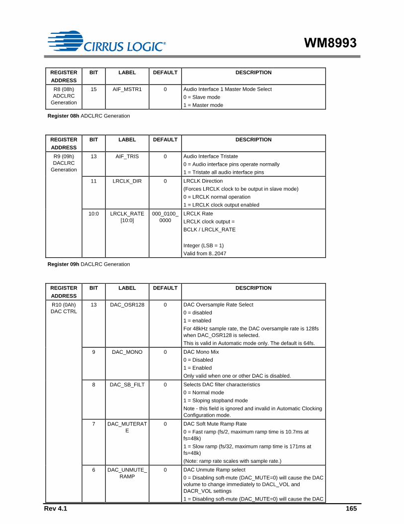
WM8993
Rev 4.1 165
REGISTER
ADDRESS
BIT LABEL DEFAULT DESCRIPTION
R8 (08h)
ADCLRC
Generation
15 AIF_MSTR1 0 Audio Interface 1 Master Mode Select
0 = Slave mode
1 = Master mode
Register 08h ADCLRC Generation
REGISTER
ADDRESS
BIT LABEL DEFAULT DESCRIPTION
R9 (09h)
DACLRC
Generation
13 AIF_TRIS 0 Audio Interface Tristate
0 = Audio interface pins operate normally
1 = Tristate all audio interface pins
11 LRCLK_DIR 0 LRCLK Direction
(Forces LRCLK clock to be output in slave mode)
0 = LRCLK normal operation
1 = LRCLK clock output enabled
10:0 LRCLK_RATE
[10:0]
000_0100_
0000
LRCLK Rate
LRCLK clock output =
BCLK / LRCLK_RATE
Integer (LSB = 1)
Valid from 8..2047
Register 09h DACLRC Generation
REGISTER
ADDRESS
BIT LABEL DEFAULT DESCRIPTION
R10 (0Ah)
DAC CTRL
13 DAC_OSR128 0 DAC Oversample Rate Select
0 = disabled
1 = enabled
For 48kHz sample rate, the DAC oversample rate is 128fs
when DAC_OSR128 is selected.
This is valid in Automatic mode only. The default is 64fs.
9 DAC_MONO 0 DAC Mono Mix
0 = Disabled
1 = Enabled
Only valid when one or other DAC is disabled.
8 DAC_SB_FILT 0 Selects DAC filter characteristics
0 = Normal mode
1 = Sloping stopband mode
Note - this field is ignored and invalid in Automatic Clocking
Configuration mode.
7 DAC_MUTERAT
E
0 DAC Soft Mute Ramp Rate
0 = Fast ramp (fs/2, maximum ramp time is 10.7ms at
fs=48k)
1 = Slow ramp (fs/32, maximum ramp time is 171ms at
fs=48k)
(Note: ramp rate scales with sample rate.)
6 DAC_UNMUTE_
RAMP
0 DAC Unmute Ramp select
0 = Disabling soft-mute (DAC_MUTE=0) will cause the DAC
volume to change immediately to DACL_VOL and
DACR_VOL settings
1 = Disabling soft-mute (DAC_MUTE=0) will cause the DAC

WM8993
Rev 4.1 166
REGISTER
ADDRESS
BIT LABEL DEFAULT DESCRIPTION
volume to ramp up gradually to the DACL_VOL and
DACR_VOL settings
5:4 DEEMPH [1:0] 00 DAC De-Emphasis Control
00 = No de-emphasis
01 = 32kHz sample rate
10 = 44.1kHz sample rate
11 = 48kHz sample rate
2 DAC_MUTE 1 DAC Soft Mute Control
0 = DAC Un-mute
1 = DAC Mute
1 DACL_DATINV 0 Left DAC Invert
0 = Left DAC output not inverted
1 = Left DAC output inverted
0 DACR_DATINV 0 Right DAC Invert
0 = Right DAC output not inverted
1 = Right DAC output inverted
Register 0Ah DAC CTRL
REGISTER
ADDRESS
BIT LABEL DEFAULT DESCRIPTION
R11 (0Bh)
Left DAC
Digital
Volume
8 DAC_VU 0 DAC Volume Update
Writing a 1 to this bit will cause left and right DAC volume to
be updated simultaneously
7:0 DACL_VOL [7:0] 1100_0000 Left DAC Digital Volume
00h = MUTE
01h = -71.625dB
… (0.375dB steps)
C0h = 0dB
Register 0Bh Left DAC Digital Volume
REGISTER
ADDRESS
BIT LABEL DEFAULT DESCRIPTION
R12 (0Ch)
Right DAC
Digital
Volume
8 DAC_VU 0 DAC Volume Update
Writing a 1 to this bit will cause left and right DAC volume to
be updated simultaneously
7:0 DACR_VOL
[7:0]
1100_0000 Right DAC Digital Volume
00h = MUTE
01h = -71.625dB
… (0.375dB steps)
C0h = 0dB
Register 0Ch Right DAC Digital Volume
REGISTER
ADDRESS
BIT LABEL DEFAULT DESCRIPTION
R13 (0Dh)
Digital Side
Tone
12:9 ADCL_DAC_SV
OL [3:0]
0000 Left Digital Sidetone Volume
0000 = -36dB
0001 = -33dB
…. (3dB steps)
1011 = -3dB

WM8993
Rev 4.1 167
REGISTER
ADDRESS
BIT LABEL DEFAULT DESCRIPTION
1100 = 0dB
8:5 ADCR_DAC_SV
OL [3:0]
0000 Right Digital Sidetone Volume
0000 = -36dB
0001 = -33dB
…. (3dB steps)
1011 = -3dB
1100 = 0dB
3:2 ADC_TO_DACL
[1:0]
00 Left DAC Digital Sidetone Source
00 = No sidetone
01 = Left ADC
10 = Right ADC
11 = Reserved
1:0 ADC_TO_DACR
[1:0]
00 Right DAC Digital Sidetone Source
00 = No sidetone
01 = Left ADC
10 = Right ADC
11 = Reserved
Register 0Dh Digital Side Tone
REGISTER
ADDRESS
BIT LABEL DEFAULT DESCRIPTION
R14 (0Eh)
ADC CTRL
9 ADC_OSR128 1 ADC Oversample Rate Select
0 = disabled
1 = enabled
For 48kHz sample rate, the ADC oversample rate is 128fs
when ADC_OSR128 is selected. Setting this bit to 0 selects
64fs mode.
Default is 128fs.
8 ADC_HPF 1 ADC Digital High Pass Filter Enable
0 = disabled
1 = enabled
6:5 ADC_HPF_CUT
[1:0]
00 ADC Digital High Pass Filter Cut-Off Frequency (fc)
00 = Hi-fi mode (fc=4Hz at fs=48kHz)
01 = Voice mode 1 (fc=127Hz at fs=16kHz)
10 = Voice mode 2 (fc=130Hz at fs=8kHz)
11 = Voice mode 3 (fc=267Hz at fs=8kHz)
(Note: fc scales with sample rate.)
1 ADCL_DATINV 0 Left ADC Invert
0 = Left ADC output not inverted
1 = Left ADC output inverted
0 ADCR_DATINV 0 Right ADC Invert
0 = Right ADC output not inverted
1 = Right ADC output inverted
Register 0Eh ADC CTRL
REGISTER
ADDRESS
BIT LABEL DEFAULT DESCRIPTION
R15 (0Fh)
Left ADC
Digital
8 ADC_VU 0 ADC Volume Update
Writing a 1 to this bit will cause left and right ADC volume to
be updated simultaneously
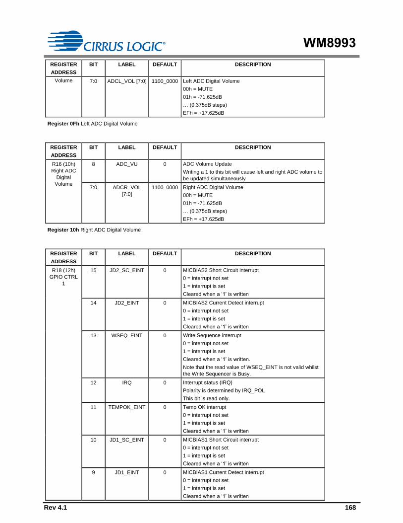
WM8993
Rev 4.1 168
REGISTER
ADDRESS
BIT LABEL DEFAULT DESCRIPTION
Volume 7:0 ADCL_VOL [7:0] 1100_0000 Left ADC Digital Volume
00h = MUTE
01h = -71.625dB
… (0.375dB steps)
EFh = +17.625dB
Register 0Fh Left ADC Digital Volume
REGISTER
ADDRESS
BIT LABEL DEFAULT DESCRIPTION
R16 (10h)
Right ADC
Digital
Volume
8 ADC_VU 0 ADC Volume Update
Writing a 1 to this bit will cause left and right ADC volume to
be updated simultaneously
7:0 ADCR_VOL
[7:0]
1100_0000 Right ADC Digital Volume
00h = MUTE
01h = -71.625dB
… (0.375dB steps)
EFh = +17.625dB
Register 10h Right ADC Digital Volume
REGISTER
ADDRESS
BIT LABEL DEFAULT DESCRIPTION
R18 (12h)
GPIO CTRL
1
15 JD2_SC_EINT 0 MICBIAS2 Short Circuit interrupt
0 = interrupt not set
1 = interrupt is set
Cleared when a ‘1’ is written
14 JD2_EINT 0 MICBIAS2 Current Detect interrupt
0 = interrupt not set
1 = interrupt is set
Cleared when a ‘1’ is written
13 WSEQ_EINT 0 Write Sequence interrupt
0 = interrupt not set
1 = interrupt is set
Cleared when a ‘1’ is written.
Note that the read value of WSEQ_EINT is not valid whilst
the Write Sequencer is Busy.
12 IRQ 0 Interrupt status (IRQ)
Polarity is determined by IRQ_POL
This bit is read only.
11 TEMPOK_EINT 0 Temp OK interrupt
0 = interrupt not set
1 = interrupt is set
Cleared when a ‘1’ is written
10 JD1_SC_EINT 0 MICBIAS1 Short Circuit interrupt
0 = interrupt not set
1 = interrupt is set
Cleared when a ‘1’ is written
9 JD1_EINT 0 MICBIAS1 Current Detect interrupt
0 = interrupt not set
1 = interrupt is set
Cleared when a ‘1’ is written

WM8993
Rev 4.1 169
REGISTER
ADDRESS
BIT LABEL DEFAULT DESCRIPTION
8 FLL_LOCK_EIN
T
0 FLL Lock interrupt
0 = interrupt not set
1 = interrupt is set
Cleared when a ‘1’ is written
7 GPI8_EINT 0 GPI8 interrupt
0 = interrupt not set
1 = interrupt is set
Cleared when a ‘1’ is written
6 GPI7_EINT 0 GPI7 interrupt
0 = interrupt not set
1 = interrupt is set
Cleared when a ‘1’ is written
0 GPIO1_EINT 0 GPIO1 interrupt
0 = interrupt not set
1 = interrupt is set
Cleared when a ‘1’ is written
Register 12h GPIO CTRL 1
REGISTER
ADDRESS
BIT LABEL DEFAULT DESCRIPTION
R19 (13h)
GPIO1 &
GPIO2
5 GPIO1_PU 0 GPIO1 pull-up resistor enable
0 = pull-up disabled
1 = pull-up enabled
4 GPIO1_PD 1 GPIO1 pull-down resistor enable
0 = pull-down disabled
1 = pull-down enabled
3:0 GPIO1_SEL
[3:0]
0000 GPIO1 function select
0000 = GPIO input
0001 = OPCLK
0010 = Logic 0
0011 = Logic 1
0100 = FLL_LOCK
0101 = TEMPOK
0110 = Reserved
0111 = IRQ
1000 = MICBIAS1 current detect
1001 = MICBIAS1 short circuit detect
1010 = MICBIAS2 current detect
1011 = MICBIAS short circuit detect
11XX = Reserved
Register 13h GPIO1 & GPIO2
REGISTER
ADDRESS
BIT LABEL DEFAULT DESCRIPTION
R20 (14h)
IRQ_DEBOU
NCE
15 JD2_SC_DB 0 MICBIAS2 Short Circuit de-bounce
0 = disabled
1 = enabled
14 JD2_DB 0 MICBIAS2 Current Detect de-bounce
0 = disabled

WM8993
Rev 4.1 170
REGISTER
ADDRESS
BIT LABEL DEFAULT DESCRIPTION
1 = enabled
13 WSEQ_DB 0 Write Sequencer de-bounce
0 = disabled
1 = enabled
11 TEMPOK_DB 0 Temp OK de-bounce
0 = disabled
1 = enabled
10 JD1_SC_DB 0 MICBIAS1 Short Circuit de-bounce
0 = disabled
1 = enabled
9 JD1_DB 0 MICBIAS1 Current Detect de-bounce
0 = disabled
1 = enabled
8 FLL_LOCK_DB 0 FLL Lock de-bounce
0 = disabled
1 = enabled
7 GPI8_DB 0 GPI8 input de-bounce
0 = disabled
1 = enabled
3 GPI7_DB 0 GPI7 input de-bounce
0 = disabled
1 = enabled
0 GPIO1_DB 0 GPIO1 input de-bounce
0 = disabled
1 = enabled
Register 14h IRQ_DEBOUNCE
REGISTER
ADDRESS
BIT LABEL DEFAULT DESCRIPTION
R21 (15h)
Input Mixer1
6 INPUTS_CLAM
P
0 Input pad VMID clamp
0 = Clamp de-activated
1 = Clamp activated
Register 15h Input Mixer1
REGISTER
ADDRESS
BIT LABEL DEFAULT DESCRIPTION
R22 (16h)
GPIOCTRL 2
13 IM_JD2_EINT 0 MICBIAS2 Current Detect interrupt mask
0 = do not mask interrupt
1 = mask interrupt
12 IM_JD2_SC_EI
NT
0 MICBIAS2 Short Circuit interrupt mask
0 = do not mask interrupt
1 = mask interrupt
11 IM_TEMPOK_EI
NT
0 Temp OK interrupt mask
0 = do not mask interrupt
1 = mask interrupt
10 IM_JD1_SC_EI
NT
0 MICBIAS1 Short Circuit interrupt mask
0 = do not mask interrupt
1 = mask interrupt
9 IM_JD1_EINT 0 MICBIAS1 Current Detect interrupt mask
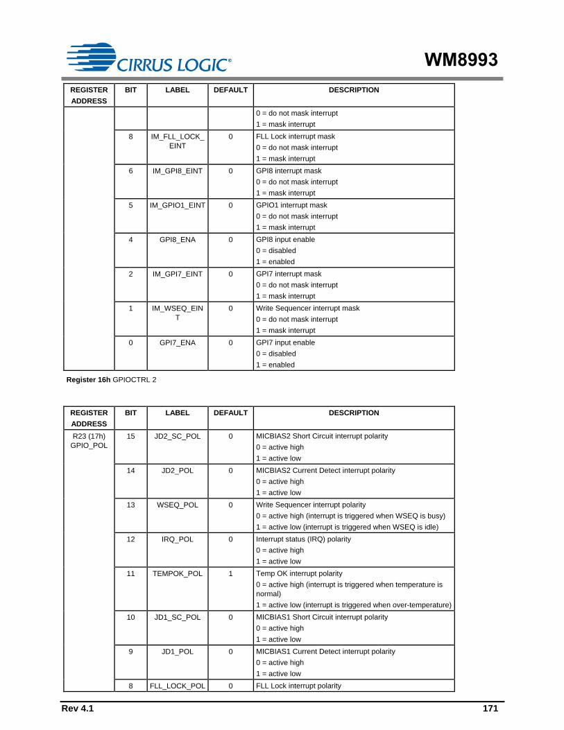
WM8993
Rev 4.1 171
REGISTER
ADDRESS
BIT LABEL DEFAULT DESCRIPTION
0 = do not mask interrupt
1 = mask interrupt
8 IM_FLL_LOCK_
EINT
0 FLL Lock interrupt mask
0 = do not mask interrupt
1 = mask interrupt
6 IM_GPI8_EINT 0 GPI8 interrupt mask
0 = do not mask interrupt
1 = mask interrupt
5 IM_GPIO1_EINT 0 GPIO1 interrupt mask
0 = do not mask interrupt
1 = mask interrupt
4 GPI8_ENA 0 GPI8 input enable
0 = disabled
1 = enabled
2 IM_GPI7_EINT 0 GPI7 interrupt mask
0 = do not mask interrupt
1 = mask interrupt
1 IM_WSEQ_EIN
T
0 Write Sequencer interrupt mask
0 = do not mask interrupt
1 = mask interrupt
0 GPI7_ENA 0 GPI7 input enable
0 = disabled
1 = enabled
Register 16h GPIOCTRL 2
REGISTER
ADDRESS
BIT LABEL DEFAULT DESCRIPTION
R23 (17h)
GPIO_POL
15 JD2_SC_POL 0 MICBIAS2 Short Circuit interrupt polarity
0 = active high
1 = active low
14 JD2_POL 0 MICBIAS2 Current Detect interrupt polarity
0 = active high
1 = active low
13 WSEQ_POL 0 Write Sequencer interrupt polarity
0 = active high (interrupt is triggered when WSEQ is busy)
1 = active low (interrupt is triggered when WSEQ is idle)
12 IRQ_POL 0 Interrupt status (IRQ) polarity
0 = active high
1 = active low
11 TEMPOK_POL 1 Temp OK interrupt polarity
0 = active high (interrupt is triggered when temperature is
normal)
1 = active low (interrupt is triggered when over-temperature)
10 JD1_SC_POL 0 MICBIAS1 Short Circuit interrupt polarity
0 = active high
1 = active low
9 JD1_POL 0 MICBIAS1 Current Detect interrupt polarity
0 = active high
1 = active low
8 FLL_LOCK_POL 0 FLL Lock interrupt polarity

WM8993
Rev 4.1 172
REGISTER
ADDRESS
BIT LABEL DEFAULT DESCRIPTION
0 = active high (interrupt is triggered when FLL Lock is
reached)
1 = active low (interrupt is triggered when FLL is not locked)
7 GPI8_POL 0 GPI8 interrupt polarity
0 = active high
1 = active low
6 GPI7_POL 0 GPI7 interrupt polarity
0 = active high
1 = active low
0 GPIO1_POL 0 GPIO1 interrupt polarity
0 = active high
1 = active low
Register 17h GPIO_POL
REGISTER
ADDRESS
BIT LABEL DEFAULT DESCRIPTION
R24 (18h)
Left Line
Input 1&2
Volume
8 IN1_VU 0 Input PGA Volume Update
Writing a 1 to this bit will cause IN1L and IN1R input PGA
volumes to be updated simultaneously
7 IN1L_MUTE 1 IN1L PGA Mute
0 = Disable Mute
1 = Enable Mute
6 IN1L_ZC 0 IN1L PGA Zero Cross Detector
0 = Change gain immediately
1 = Change gain on zero cross only
4:0 IN1L_VOL [4:0] 0_1011 IN1L Volume
00000 = -16.5dB
00001 = -15dB
...
11110 = +28.5dB
11111 = +30dB
Register 18h Left Line Input 1&2 Volume
REGISTER
ADDRESS
BIT LABEL DEFAULT DESCRIPTION
R25 (19h)
Left Line
Input 3&4
Volume
8 IN2_VU 0 Input PGA Volume Update
Writing a 1 to this bit will cause IN2L and IN2R input PGA
volumes to be updated simultaneously
7 IN2L_MUTE 1 IN2L PGA Mute
0 = Disable Mute
1 = Enable Mute
6 IN2L_ZC 0 IN2L PGA Zero Cross Detector
0 = Change gain immediately
1 = Change gain on zero cross only
4:0 IN2L_VOL [4:0] 0_1011 IN2L Volume
00000 = -16.5dB
00001 = -15dB
...
11110 = +28.5dB
11111 = +30dB

WM8993
Rev 4.1 173
Register 19h Left Line Input 3&4 Volume
REGISTER
ADDRESS
BIT LABEL DEFAULT DESCRIPTION
R26 (1Ah)
Right Line
Input 1&2
Volume
8 IN1_VU 0 Input PGA Volume Update
Writing a 1 to this bit will cause IN1L and IN1R input PGA
volumes to be updated simultaneously
7 IN1R_MUTE 1 IN1R PGA Mute
0 = Disable Mute
1 = Enable Mute
6 IN1R_ZC 0 IN1R PGA Zero Cross Detector
0 = Change gain immediately
1 = Change gain on zero cross only
4:0 IN1R_VOL [4:0] 0_1011 IN1R Volume
00000 = -16.5dB
00001 = -15dB
...
11110 = +28.5dB
11111 = +30dB
Register 1Ah Right Line Input 1&2 Volume
REGISTER
ADDRESS
BIT LABEL DEFAULT DESCRIPTION
R27 (1Bh)
Right Line
Input 3&4
Volume
8 IN2_VU 0 Input PGA Volume Update
Writing a 1 to this bit will cause IN2L and IN2R input PGA
volumes to be updated simultaneously
7 IN2R_MUTE 1 IN2R PGA Mute
0 = Disable Mute
1 = Enable Mute
6 IN2R_ZC 0 IN2R PGA Zero Cross Detector
0 = Change gain immediately
1 = Change gain on zero cross only
4:0 IN2R_VOL [4:0] 0_1011 IN2R Volume
00000 = -16.5dB
00001 = -15dB
...
11110 = +28.5dB
11111 = +30dB
Register 1Bh Right Line Input 3&4 Volume
REGISTER
ADDRESS
BIT LABEL DEFAULT DESCRIPTION
R28 (1Ch)
Left Output
Volume
8 HPOUT1_VU 0 Headphone Output PGA Volume Update
Writing a 1 to this bit will update HPOUT1LVOL and
HPOUT1RVOL volumes simultaneously.
7 HPOUT1L_ZC 0 HPOUT1LVOL (Left Headphone Output PGA) Zero Cross
Enable
0 = Zero cross disabled
1 = Zero cross enabled
6 HPOUT1L_MUT
E_N
1 HPOUT1LVOL (Left Headphone Output PGA) Mute
0 = Mute
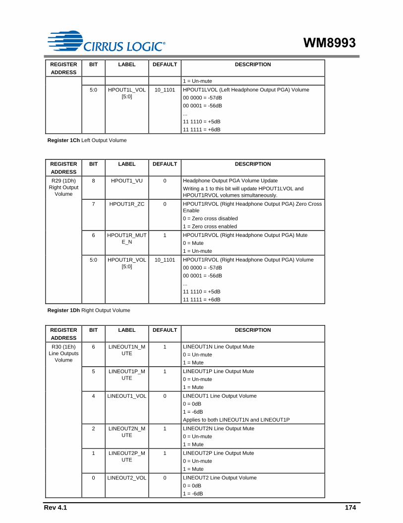
WM8993
Rev 4.1 174
REGISTER
ADDRESS
BIT LABEL DEFAULT DESCRIPTION
1 = Un-mute
5:0 HPOUT1L_VOL
[5:0]
10_1101 HPOUT1LVOL (Left Headphone Output PGA) Volume
00 0000 = -57dB
00 0001 = -56dB
...
11 1110 = +5dB
11 1111 = +6dB
Register 1Ch Left Output Volume
REGISTER
ADDRESS
BIT LABEL DEFAULT DESCRIPTION
R29 (1Dh)
Right Output
Volume
8 HPOUT1_VU 0 Headphone Output PGA Volume Update
Writing a 1 to this bit will update HPOUT1LVOL and
HPOUT1RVOL volumes simultaneously.
7 HPOUT1R_ZC 0 HPOUT1RVOL (Right Headphone Output PGA) Zero Cross
Enable
0 = Zero cross disabled
1 = Zero cross enabled
6 HPOUT1R_MUT
E_N
1 HPOUT1RVOL (Right Headphone Output PGA) Mute
0 = Mute
1 = Un-mute
5:0 HPOUT1R_VOL
[5:0]
10_1101 HPOUT1RVOL (Right Headphone Output PGA) Volume
00 0000 = -57dB
00 0001 = -56dB
...
11 1110 = +5dB
11 1111 = +6dB
Register 1Dh Right Output Volume
REGISTER
ADDRESS
BIT LABEL DEFAULT DESCRIPTION
R30 (1Eh)
Line Outputs
Volume
6 LINEOUT1N_M
UTE
1 LINEOUT1N Line Output Mute
0 = Un-mute
1 = Mute
5 LINEOUT1P_M
UTE
1 LINEOUT1P Line Output Mute
0 = Un-mute
1 = Mute
4 LINEOUT1_VOL 0 LINEOUT1 Line Output Volume
0 = 0dB
1 = -6dB
Applies to both LINEOUT1N and LINEOUT1P
2 LINEOUT2N_M
UTE
1 LINEOUT2N Line Output Mute
0 = Un-mute
1 = Mute
1 LINEOUT2P_M
UTE
1 LINEOUT2P Line Output Mute
0 = Un-mute
1 = Mute
0 LINEOUT2_VOL 0 LINEOUT2 Line Output Volume
0 = 0dB
1 = -6dB

WM8993
Rev 4.1 175
REGISTER
ADDRESS
BIT LABEL DEFAULT DESCRIPTION
Applies to both LINEOUT2N and LINEOUT2P
Register 1Eh Line Outputs Volume
REGISTER
ADDRESS
BIT LABEL DEFAULT DESCRIPTION
R31 (1Fh)
HPOUT2
Volume
5 HPOUT2_MUTE 1 HPOUT2 (Earpiece Driver) Mute
0 = Un-mute
1 = Mute
4 HPOUT2_VOL 0 HPOUT2 (Earpiece Driver) Volume
0 = 0dB
1 = -6dB
Register 1Fh HPOUT2 Volume
REGISTER
ADDRESS
BIT LABEL DEFAULT DESCRIPTION
R32 (20h)
Left OPGA
Volume
8 MIXOUT_VU 0 Mixer Output PGA Volume Update
Writing a 1 to this bit will update MIXOUTLVOL and
MIXOUTRVOL volumes simultaneously.
7 MIXOUTL_ZC 0 MIXOUTLVOL (Left Mixer Output PGA) Zero Cross Enable
0 = Zero cross disabled
1 = Zero cross enabled
6 MIXOUTL_MUT
E_N
1 MIXOUTLVOL (Left Mixer Output PGA) Mute
0 = Mute
1 = Un-mute
5:0 MIXOUTL_VOL
[5:0]
11_1001 MIXOUTLVOL (Left Mixer Output PGA) Volume
00 0000 = -57dB
00 0001 = -56dB
...
11 1110 = +5dB
11 1111 = +6dB
Register 20h Left OPGA Volume
REGISTER
ADDRESS
BIT LABEL DEFAULT DESCRIPTION
R33 (21h)
Right OPGA
Volume
8 MIXOUT_VU 0 Mixer Output PGA Volume Update
Writing a 1 to this bit will update MIXOUTLVOL and
MIXOUTRVOL volumes simultaneously.
7 MIXOUTR_ZC 0 MIXOUTRVOL (Right Mixer Output PGA) Zero Cross
Enable
0 = Zero cross disabled
1 = Zero cross enabled
6 MIXOUTR_MUT
E_N
1 MIXOUTLVOL (Right Mixer Output PGA) Mute
0 = Mute
1 = Un-mute
5:0 MIXOUTR_VOL
[5:0]
11_1001 MIXOUTRVOL (Right Mixer Output PGA) Volume
00 0000 = -57dB
00 0001 = -56dB
...
11 1110 = +5dB

WM8993
Rev 4.1 176
REGISTER
ADDRESS
BIT LABEL DEFAULT DESCRIPTION
11 1111 = +6dB
Register 21h Right OPGA Volume
REGISTER
ADDRESS
BIT LABEL DEFAULT DESCRIPTION
R34 (22h)
SPKMIXL
Attenuation
5 MIXINL_SPKMI
XL_VOL
0 MIXINL (Left ADC bypass) to SPKMIXL Fine Volume
Control
0 = 0dB
1 = -3dB
4 IN1LP_SPKMIX
L_VOL
0 IN1LP to SPKMIXL Fine Volume Control
0 = 0dB
1 = -3dB
3 MIXOUTL_SPK
MIXL_VOL
0 Left Mixer Output to SPKMIXL Fine Volume Control
0 = 0dB
1 = -3dB
2 DACL_SPKMIX
L_VOL
0 Left DAC to SPKMIXL Fine Volume Control
0 = 0dB
1 = -3dB
1:0 SPKMIXL_VOL
[1:0]
11 Left Speaker Mixer Volume Control
00 = 0dB
01 = -6dB
10 = -12dB
11 = mute
Register 22h SPKMIXL Attenuation
REGISTER
ADDRESS
BIT LABEL DEFAULT DESCRIPTION
R35 (23h)
SPKMIXR
Attenuation
8 SPKOUT_CLAS
SAB_MODE
0 Speaker Class AB Mode Enable
0 = Class D mode
1 = Class AB mode
5 MIXINR_SPKMI
XR_VOL
0 MIXINR (Right ADC bypass) to SPKMIXR Fine Volume
Control
0 = 0dB
1 = -3dB
4 IN1RP_SPKMIX
R_VOL
0 IN1RP to SPKMIXR Fine Volume Control
0 = 0dB
1 = -3dB
3 MIXOUTR_SPK
MIXR_VOL
0 Right Mixer Output to SPKMIXR Fine Volume Control
0 = 0dB
1 = -3dB
2 DACR_SPKMIX
R_VOL
0 Right DAC to SPKMIXR Fine Volume Control
0 = 0dB
1 = -3dB
1:0 SPKMIXR_VOL
[1:0]
11 Right Speaker Mixer Volume Control
00 = 0dB
01 = -6dB
10 = -12dB
11 = mute
Register 23h SPKMIXR Attenuation
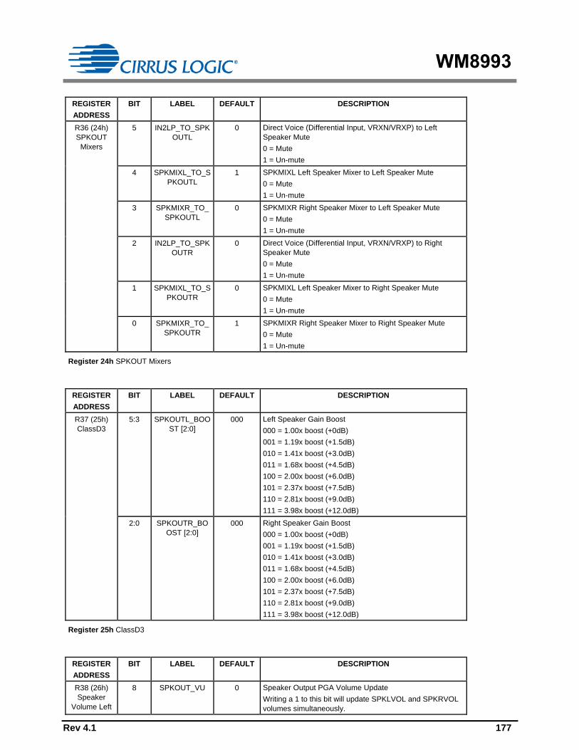
WM8993
Rev 4.1 177
REGISTER
ADDRESS
BIT LABEL DEFAULT DESCRIPTION
R36 (24h)
SPKOUT
Mixers
5 IN2LP_TO_SPK
OUTL
0 Direct Voice (Differential Input, VRXN/VRXP) to Left
Speaker Mute
0 = Mute
1 = Un-mute
4 SPKMIXL_TO_S
PKOUTL
1 SPKMIXL Left Speaker Mixer to Left Speaker Mute
0 = Mute
1 = Un-mute
3 SPKMIXR_TO_
SPKOUTL
0 SPKMIXR Right Speaker Mixer to Left Speaker Mute
0 = Mute
1 = Un-mute
2 IN2LP_TO_SPK
OUTR
0 Direct Voice (Differential Input, VRXN/VRXP) to Right
Speaker Mute
0 = Mute
1 = Un-mute
1 SPKMIXL_TO_S
PKOUTR
0 SPKMIXL Left Speaker Mixer to Right Speaker Mute
0 = Mute
1 = Un-mute
0 SPKMIXR_TO_
SPKOUTR
1 SPKMIXR Right Speaker Mixer to Right Speaker Mute
0 = Mute
1 = Un-mute
Register 24h SPKOUT Mixers
REGISTER
ADDRESS
BIT LABEL DEFAULT DESCRIPTION
R37 (25h)
ClassD3
5:3 SPKOUTL_BOO
ST [2:0]
000 Left Speaker Gain Boost
000 = 1.00x boost (+0dB)
001 = 1.19x boost (+1.5dB)
010 = 1.41x boost (+3.0dB)
011 = 1.68x boost (+4.5dB)
100 = 2.00x boost (+6.0dB)
101 = 2.37x boost (+7.5dB)
110 = 2.81x boost (+9.0dB)
111 = 3.98x boost (+12.0dB)
2:0 SPKOUTR_BO
OST [2:0]
000 Right Speaker Gain Boost
000 = 1.00x boost (+0dB)
001 = 1.19x boost (+1.5dB)
010 = 1.41x boost (+3.0dB)
011 = 1.68x boost (+4.5dB)
100 = 2.00x boost (+6.0dB)
101 = 2.37x boost (+7.5dB)
110 = 2.81x boost (+9.0dB)
111 = 3.98x boost (+12.0dB)
Register 25h ClassD3
REGISTER
ADDRESS
BIT LABEL DEFAULT DESCRIPTION
R38 (26h)
Speaker
Volume Left
8 SPKOUT_VU 0 Speaker Output PGA Volume Update
Writing a 1 to this bit will update SPKLVOL and SPKRVOL
volumes simultaneously.

WM8993
Rev 4.1 178
REGISTER
ADDRESS
BIT LABEL DEFAULT DESCRIPTION
7 SPKOUTL_ZC 0 SPKLVOL (Left Speaker Output PGA) Zero Cross Enable
0 = Zero cross disabled
1 = Zero cross enabled
6 SPKOUTL_MUT
E_N
1 SPKLVOL (Left Speaker Output PGA) Mute
0 = Mute
1 = Un-mute
5:0 SPKOUTL_VOL
[5:0]
11_1001 SPKLVOL (Left Speaker Output PGA) Volume
00 0000 = -57dB
00 0001 = -56dB
...
11 1110 = +5dB
11 1111 = +6dB
Register 26h Speaker Volume Left
REGISTER
ADDRESS
BIT LABEL DEFAULT DESCRIPTION
R39 (27h)
Speaker
Volume Right
8 SPKOUT_VU 0 Speaker Output PGA Volume Update
Writing a 1 to this bit will update SPKLVOL and SPKRVOL
volumes simultaneously.
7 SPKOUTR_ZC 0 SPKRVOL (Right Speaker Output PGA) Zero Cross Enable
0 = Zero cross disabled
1 = Zero cross enabled
6 SPKOUTR_MUT
E_N
1 SPKRVOL (Right Speaker Output PGA) Mute
0 = Mute
1 = Un-mute
5:0 SPKOUTR_VOL
[5:0]
11_1001 SPKRVOL (Right Speaker Output PGA) Volume
00 0000 = -57dB
00 0001 = -56dB
...
11 1110 = +5dB
11 1111 = +6dB
Register 27h Speaker Volume Right
REGISTER
ADDRESS
BIT LABEL DEFAULT DESCRIPTION
R40 (28h)
Input Mixer2
7 IN2LP_TO_IN2L 0 IN2L PGA Non-Inverting Input Select
0 = Connected to VMID
1 = Connected to IN2LP
Note that VMID_BUF_ENA must be set when using IN2L
connected to VMID.
6 IN2LN_TO_IN2L 0 IN2L PGA Inverting Input Select
0 = Not connected
1 = Connected to IN2LN
5 IN1LP_TO_IN1L 0 IN1L PGA Non-Inverting Input Select
0 = Connected to VMID
1 = Connected to IN1LP
Note that VMID_BUF_ENA must be set when using IN2L
connected to VMID.
4 IN1LN_TO_IN1L 0 IN1L PGA Inverting Input Select
0 = Not connected

WM8993
Rev 4.1 179
REGISTER
ADDRESS
BIT LABEL DEFAULT DESCRIPTION
1 = Connected to IN1LN
3 IN2RP_TO_IN2
R
0 IN2R PGA Non-Inverting Input Select
0 = Connected to VMID
1 = Connected to IN2RP
Note that VMID_BUF_ENA must be set when using IN2L
connected to VMID.
2 IN2RN_TO_IN2
R
0 IN2R PGA Inverting Input Select
0 = Not connected
1 = Connected to IN2RN
1 IN1RP_TO_IN1
R
0 IN1R PGA Non-Inverting Input Select
0 = Connected to VMID
1 = Connected to IN1RP
Note that VMID_BUF_ENA must be set when using IN2L
connected to VMID.
0 IN1RN_TO_IN1
R
0 IN1R PGA Inverting Input Select
0 = Not connected
1 = Connected to IN1RN
Register 28h Input Mixer2
REGISTER
ADDRESS
BIT LABEL DEFAULT DESCRIPTION
R41 (29h)
Input Mixer3
8 IN2L_TO_MIXIN
L
0 IN2L PGA Output to MIXINL Mute
0 = Mute
1 = Un-Mute
7 IN2L_MIXINL_V
OL
0 IN2L PGA Output to MIXINL Gain
0 = 0dB
1 = +30dB
5 IN1L_TO_MIXIN
L
0 IN1L PGA Output to MIXINL Mute
0 = Mute
1 = Un-Mute
4 IN1L_MIXINL_V
OL
0 IN1L PGA Output to MIXINL Gain
0 = 0dB
1 = +30dB
2:0 MIXOUTL_MIXI
NL_VOL [2:0]
000 Record Path MIXOUTL to MIXINL Gain and Mute
000 = Mute
001 = -12dB
010 = -9dB
011 = -6dB
100 = -3dB
101 = 0dB
110 = +3dB
111 = +6dB
Register 29h Input Mixer3
REGISTER
ADDRESS
BIT LABEL DEFAULT DESCRIPTION
R42 (2Ah)
Input Mixer4
8 IN2R_TO_MIXIN
R
0 IN2R PGA Output to MIXINR Mute
0 = Mute
1 = Un-Mute
7 IN2R_MIXINR_ 0 IN2R PGA Output to MIXINR Gain

WM8993
Rev 4.1 180
REGISTER
ADDRESS
BIT LABEL DEFAULT DESCRIPTION
VOL 0 = 0dB
1 = +30dB
5 IN1R_TO_MIXIN
R
0 IN1R PGA Output to MIXINR Mute
0 = Mute
1 = Un-Mute
4 IN1R_MIXINR_
VOL
0 IN1R PGA Output to MIXINR Gain
0 = 0dB
1 = +30dB
2:0 MIXOUTR_MIXI
NR_VOL [2:0]
000 Record Path MIXOUTR to MIXINR Gain and Mute
000 = Mute
001 = -12dB
010 = -9dB
011 = -6dB
100 = -3dB
101 = 0dB
110 = +3dB
111 = +6dB
Register 2Ah Input Mixer4
REGISTER
ADDRESS
BIT LABEL DEFAULT DESCRIPTION
R43 (2Bh)
Input Mixer5
8:6 IN1LP_MIXINL_
VOL [2:0]
000 IN1LP Pin (PGA Bypass) to MIXINL Gain and Mute
000 = Mute
001 = -12dB
010 = -9dB
011 = -6dB
100 = -3dB
101 = 0dB
110 = +3dB
111 = +6dB
2:0 IN2LP_MIXINL_
VOL [2:0]
000 RXVOICE (VRXN/VRXP) Differential Input to MIXINL Gain
and Mute
000 = Mute
001 = -12dB
010 = -9dB
011 = -6dB
100 = -3dB
101 = 0dB
110 = +3dB
111 = +6dB
Register 2Bh Input Mixer5
REGISTER
ADDRESS
BIT LABEL DEFAULT DESCRIPTION
R44 (2Ch)
Input Mixer6
8:6 IN1RP_MIXINR
_VOL [2:0]
000 IN1RP Pin (PGA Bypass) to MIXINR Gain and Mute
000 = Mute
001 = -12dB
010 = -9dB
011 = -6dB
100 = -3dB

WM8993
Rev 4.1 181
REGISTER
ADDRESS
BIT LABEL DEFAULT DESCRIPTION
101 = 0dB
110 = +3dB
111 = +6dB
2:0 IN2LP_MIXINR_
VOL [2:0]
000 RXVOICE (VRXN/VRXP) Differential Input to MIXINR Gain
and Mute
000 = Mute
001 = -12dB
010 = -9dB
011 = -6dB
100 = -3dB
101 = 0dB
110 = +3dB
111 = +6dB
Register 2Ch Input Mixer6
REGISTER
ADDRESS
BIT LABEL DEFAULT DESCRIPTION
R45 (2Dh)
Output
Mixer1
8 DACL_TO_HPO
UT1L
0 HPOUT1LVOL (Left Headphone Output PGA) Input Select
0 = MIXOUTL
1 = DACL
7 MIXINR_TO_MI
XOUTL
0 MIXINR Output (Right ADC bypass) to MIXOUTL Mute
0 = Mute
1 = Un-mute
6 MIXINL_TO_MI
XOUTL
0 MIXINL Output (Left ADC bypass) to MIXOUTL Mute
0 = Mute
1 = Un-mute
5 IN2RN_TO_MIX
OUTL
0 IN2RN to MIXOUTL Mute
0 = Mute
1 = Un-mute
4 IN2LN_TO_MIX
OUTL
0 IN2LN to MIXOUTL Mute
0 = Mute
1 = Un-mute
3 IN1R_TO_MIXO
UTL
0 IN1R PGA Output to MIXOUTL Mute
0 = Mute
1 = Un-mute
2 IN1L_TO_MIXO
UTL
0 IN1L PGA Output to MIXOUTL Mute
0 = Mute
1 = Un-mute
1 IN2LP_TO_MIX
OUTL
0 IN2LP to MIXOUTL Mute
0 = Mute
1 = Un-mute
0 DACL_TO_MIX
OUTL
0 Left DAC to MIXOUTL Mute
0 = Mute
1 = Un-mute
Register 2Dh Output Mixer1
REGISTER
ADDRESS
BIT LABEL DEFAULT DESCRIPTION
R46 (2Eh)
Output
8 DACR_TO_HPO
UT1R
0 HPOUT1RVOL (Right Headphone Output PGA) Input
Select

WM8993
Rev 4.1 182
REGISTER
ADDRESS
BIT LABEL DEFAULT DESCRIPTION
Mixer2 0 = MIXOUTR
1 = DACR
7 MIXINL_TO_MI
XOUTR
0 MIXINL Output (Left ADC bypass) to MIXOUTR Mute
0 = Mute
1 = Un-mute
6 MIXINR_TO_MI
XOUTR
0 MIXINR Output (Right ADC bypass) to MIXOUTR Mute
0 = Mute
1 = Un-mute
5 IN2LN_TO_MIX
OUTR
0 IN2LN to MIXOUTR Mute
0 = Mute
1 = Un-mute
4 IN2RN_TO_MIX
OUTR
0 IN2RN to MIXOUTR Mute
0 = Mute
1 = Un-mute
3 IN1L_TO_MIXO
UTR
0 IN1L PGA Output to MIXOUTR Mute
0 = Mute
1 = Un-mute
2 IN1R_TO_MIXO
UTR
0 IN1R PGA Output to MIXOUTR Mute
0 = Mute
1 = Un-mute
1 IN2RP_TO_MIX
OUTR
0 IN2RP to MIXOUTR Mute
0 = Mute
1 = Un-mute
0 DACR_TO_MIX
OUTR
0 Right DAC to MIXOUTR Mute
0 = Mute
1 = Un-mute
Register 2Eh Output Mixer2
REGISTER
ADDRESS
BIT LABEL DEFAULT DESCRIPTION
R47 (2Fh)
Output
Mixer3
11:9 IN2LP_MIXOUT
L_VOL [2:0]
000 IN2LP to MIXOUTL Volume
0dB to -21dB in 3dB steps
000 = 0dB
001 = -3dB
...
110 = -18dB
111 = -21dB
8:6 IN2LN_MIXOUT
L_VOL [2:0]
000 IN2LN to MIXOUTL Volume
0dB to -21dB in 3dB steps
000 = 0dB
001 = -3dB
...
110 = -18dB
111 = -21dB
5:3 IN1R_MIXOUTL
_VOL [2:0]
000 IN1R PGA Output to MIXOUTL Volume
0dB to -21dB in 3dB steps
000 = 0dB
001 = -3dB
...
110 = -18dB
111 = -21dB

WM8993
Rev 4.1 183
REGISTER
ADDRESS
BIT LABEL DEFAULT DESCRIPTION
2:0 IN1L_MIXOUTL
_VOL [2:0]
000 IN1L PGA Output to MIXOUTL Volume
0dB to -21dB in 3dB steps
000 = 0dB
001 = -3dB
...
110 = -18dB
111 = -21dB
Register 2Fh Output Mixer3
REGISTER
ADDRESS
BIT LABEL DEFAULT DESCRIPTION
R48 (30h)
Output
Mixer4
11:9 IN2RP_MIXOUT
R_VOL [2:0]
000 IN2RP to MIXOUTR Volume
0dB to -21dB in 3dB steps
000 = 0dB
001 = -3dB
...
110 = -18dB
111 = -21dB
8:6 IN2RN_MIXOUT
R_VOL [2:0]
000 IN2RN to MIXOUTR Volume
0dB to -21dB in 3dB steps
000 = 0dB
001 = -3dB
...
110 = -18dB
111 = -21dB
5:3 IN1L_MIXOUTR
_VOL [2:0]
000 IN1L PGA Output to MIXOUTR Volume
0dB to -21dB in 3dB steps
000 = 0dB
001 = -3dB
...
110 = -18dB
111 = -21dB
2:0 IN1R_MIXOUTR
_VOL [2:0]
000 IN1R PGA Output to MIXOUTR Volume
0dB to -21dB in 3dB steps
000 = 0dB
001 = -3dB
...
110 = -18dB
111 = -21dB
Register 30h Output Mixer4
REGISTER
ADDRESS
BIT LABEL DEFAULT DESCRIPTION
R49 (31h)
Output
Mixer5
11:9 DACL_MIXOUT
L_VOL [2:0]
000 Left DAC to MIXOUTL Volume
0dB to -21dB in 3dB steps
000 = 0dB
001 = -3dB
...
110 = -18dB
111 = -21dB
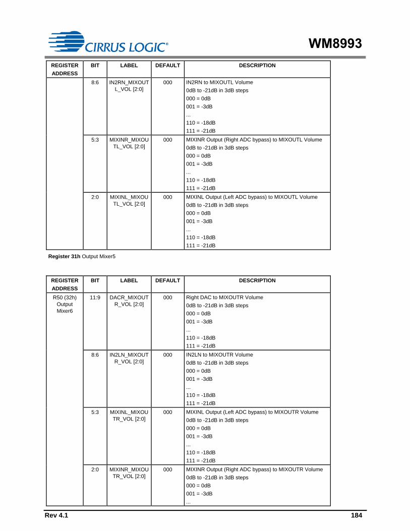
WM8993
Rev 4.1 184
REGISTER
ADDRESS
BIT LABEL DEFAULT DESCRIPTION
8:6 IN2RN_MIXOUT
L_VOL [2:0]
000 IN2RN to MIXOUTL Volume
0dB to -21dB in 3dB steps
000 = 0dB
001 = -3dB
...
110 = -18dB
111 = -21dB
5:3 MIXINR_MIXOU
TL_VOL [2:0]
000 MIXINR Output (Right ADC bypass) to MIXOUTL Volume
0dB to -21dB in 3dB steps
000 = 0dB
001 = -3dB
...
110 = -18dB
111 = -21dB
2:0 MIXINL_MIXOU
TL_VOL [2:0]
000 MIXINL Output (Left ADC bypass) to MIXOUTL Volume
0dB to -21dB in 3dB steps
000 = 0dB
001 = -3dB
...
110 = -18dB
111 = -21dB
Register 31h Output Mixer5
REGISTER
ADDRESS
BIT LABEL DEFAULT DESCRIPTION
R50 (32h)
Output
Mixer6
11:9 DACR_MIXOUT
R_VOL [2:0]
000 Right DAC to MIXOUTR Volume
0dB to -21dB in 3dB steps
000 = 0dB
001 = -3dB
...
110 = -18dB
111 = -21dB
8:6 IN2LN_MIXOUT
R_VOL [2:0]
000 IN2LN to MIXOUTR Volume
0dB to -21dB in 3dB steps
000 = 0dB
001 = -3dB
...
110 = -18dB
111 = -21dB
5:3 MIXINL_MIXOU
TR_VOL [2:0]
000 MIXINL Output (Left ADC bypass) to MIXOUTR Volume
0dB to -21dB in 3dB steps
000 = 0dB
001 = -3dB
...
110 = -18dB
111 = -21dB
2:0 MIXINR_MIXOU
TR_VOL [2:0]
000 MIXINR Output (Right ADC bypass) to MIXOUTR Volume
0dB to -21dB in 3dB steps
000 = 0dB
001 = -3dB
...

WM8993
Rev 4.1 185
REGISTER
ADDRESS
BIT LABEL DEFAULT DESCRIPTION
110 = -18dB
111 = -21dB
Register 32h Output Mixer6
REGISTER
ADDRESS
BIT LABEL DEFAULT DESCRIPTION
R51 (33h)
HPOUT2
Mixer
5 IN2LRP_TO_HP
OUT2
0 Direct Voice (Differential Input, VRXN/VRXP) to Earpiece
Driver
0 = Mute
1 = Un-mute
4 MIXOUTLVOL_
TO_HPOUT2
0 MIXOUTLVOL (Left Output Mixer PGA) to Earpiece Driver
0 = Mute
1 = Un-mute
3 MIXOUTRVOL_
TO_HPOUT2
0 MIXOUTRVOL (Right Output Mixer PGA) to Earpiece Driver
0 = Mute
1 = Un-mute
Register 33h HPOUT2 Mixer
REGISTER
ADDRESS
BIT LABEL DEFAULT DESCRIPTION
R52 (34h)
Line Mixer1
6 MIXOUTL_TO_L
INEOUT1N
0 MIXOUTL to Single-Ended Line Output on LINEOUT1N
0 = Mute
1 = Un-mute
(LINEOUT1_MODE = 1)
5 MIXOUTR_TO_
LINEOUT1N
0 MIXOUTR to Single-Ended Line Output on LINEOUT1N
0 = Mute
1 = Un-mute
(LINEOUT1_MODE = 1)
4 LINEOUT1_MO
DE
0 LINEOUT1 Mode Select
0 = Differential
1 = Single-Ended
2 IN1R_TO_LINE
OUT1P
0 IN1R Input PGA to Differential Line Output on LINEOUT1
0 = Mute
1 = Un-mute
(LINEOUT1_MODE = 0)
1 IN1L_TO_LINE
OUT1P
0 IN1L Input PGA to Differential Line Output on LINEOUT1
0 = Mute
1 = Un-mute
(LINEOUT1_MODE = 0)
0 MIXOUTL_TO_L
INEOUT1P
0 Differential Mode (LINEOUT1_MODE = 0):
MIXOUTL to Differential Output on LINEOUT1
0 = Mute
1 = Un-mute
Single Ended Mode (LINEOUT1_MODE = 1):
MIXOUTL to Single-Ended Line Output on LINEOUT1P
0 = Mute
1 = Un-mute
Register 34h Line Mixer1
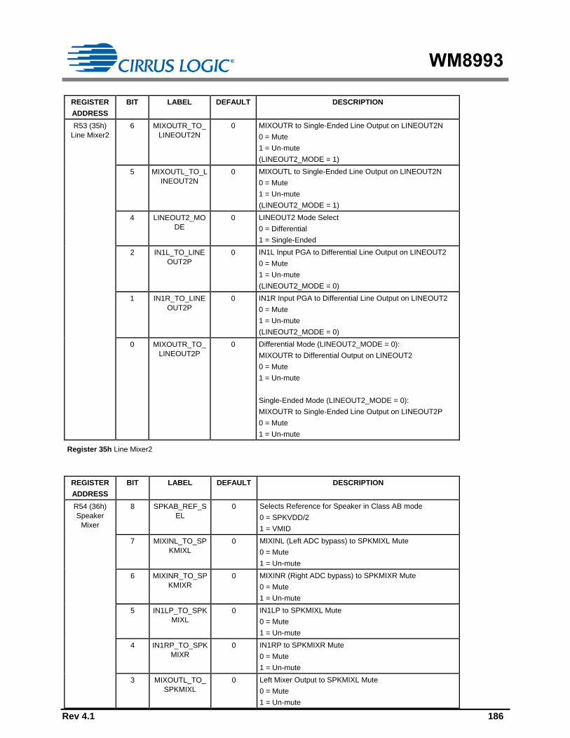
WM8993
Rev 4.1 186
REGISTER
ADDRESS
BIT LABEL DEFAULT DESCRIPTION
R53 (35h)
Line Mixer2
6 MIXOUTR_TO_
LINEOUT2N
0 MIXOUTR to Single-Ended Line Output on LINEOUT2N
0 = Mute
1 = Un-mute
(LINEOUT2_MODE = 1)
5 MIXOUTL_TO_L
INEOUT2N
0 MIXOUTL to Single-Ended Line Output on LINEOUT2N
0 = Mute
1 = Un-mute
(LINEOUT2_MODE = 1)
4 LINEOUT2_MO
DE
0 LINEOUT2 Mode Select
0 = Differential
1 = Single-Ended
2 IN1L_TO_LINE
OUT2P
0 IN1L Input PGA to Differential Line Output on LINEOUT2
0 = Mute
1 = Un-mute
(LINEOUT2_MODE = 0)
1 IN1R_TO_LINE
OUT2P
0 IN1R Input PGA to Differential Line Output on LINEOUT2
0 = Mute
1 = Un-mute
(LINEOUT2_MODE = 0)
0 MIXOUTR_TO_
LINEOUT2P
0 Differential Mode (LINEOUT2_MODE = 0):
MIXOUTR to Differential Output on LINEOUT2
0 = Mute
1 = Un-mute
Single-Ended Mode (LINEOUT2_MODE = 0):
MIXOUTR to Single-Ended Line Output on LINEOUT2P
0 = Mute
1 = Un-mute
Register 35h Line Mixer2
REGISTER
ADDRESS
BIT LABEL DEFAULT DESCRIPTION
R54 (36h)
Speaker
Mixer
8 SPKAB_REF_S
EL
0 Selects Reference for Speaker in Class AB mode
0 = SPKVDD/2
1 = VMID
7 MIXINL_TO_SP
KMIXL
0 MIXINL (Left ADC bypass) to SPKMIXL Mute
0 = Mute
1 = Un-mute
6 MIXINR_TO_SP
KMIXR
0 MIXINR (Right ADC bypass) to SPKMIXR Mute
0 = Mute
1 = Un-mute
5 IN1LP_TO_SPK
MIXL
0 IN1LP to SPKMIXL Mute
0 = Mute
1 = Un-mute
4 IN1RP_TO_SPK
MIXR
0 IN1RP to SPKMIXR Mute
0 = Mute
1 = Un-mute
3 MIXOUTL_TO_
SPKMIXL
0 Left Mixer Output to SPKMIXL Mute
0 = Mute
1 = Un-mute

WM8993
Rev 4.1 187
REGISTER
ADDRESS
BIT LABEL DEFAULT DESCRIPTION
2 MIXOUTR_TO_
SPKMIXR
0 Right Mixer Output to SPKMIXR Mute
0 = Mute
1 = Un-mute
1 DACL_TO_SPK
MIXL
0 Left DAC to SPKMIXL Mute
0 = Mute
1 = Un-mute
0 DACR_TO_SPK
MIXR
0 Right DAC to SPKMIXR Mute
0 = Mute
1 = Un-mute
Register 36h Speaker Mixer
REGISTER
ADDRESS
BIT LABEL DEFAULT DESCRIPTION
R55 (37h)
Additional
Control
7 LINEOUT1_FB 0 Enable ground loop noise feedback on LINEOUT1
0 = Disabled
1 = Enabled
6 LINEOUT2_FB 0 Enable ground loop noise feedback on LINEOUT2
0 = Disabled
1 = Enabled
0 VROI 0 Buffered VMID to Analogue Line Output Resistance
(Disabled Outputs)
0 = 20kohm from buffered VMID to output
1 = 1000ohm from buffered VMID to output
Register 37h Additional Control
REGISTER
ADDRESS
BIT LABEL DEFAULT DESCRIPTION
R56 (38h)
AntiPOP1
7 LINEOUT_VMID
_BUF_ENA
0 Enables VMID reference for line outputs in single-ended
mode
0 = Disabled
1 = Enabled
6 HPOUT2_IN_EN
A
0 HPOUT2MIX Mixer and Input Stage Enable
0 = Disabled
1 = Enabled
5 LINEOUT1_DIS
CH
0 Discharges LINEOUT1P and LINEOUT1N outputs via
0 = Not active
1 = Actively discharging LINEOUT1P and LINEOUT1N
4 LINEOUT2_DIS
CH
0 Discharges LINEOUT2P and LINEOUT2N outputs via
0 = Not active
1 = Actively discharging LINEOUT2P and LINEOUT2N
Register 38h AntiPOP1

WM8993
Rev 4.1 188
REGISTER
ADDRESS
BIT LABEL DEFAULT DESCRIPTION
R57 (39h)
AntiPOP2
6:5 VMID_RAMP
[1:0]
00 VMID soft start enable / slew rate control
00 = Normal / Slow start
01 = Normal / Fast start
10 = Soft / Slow start
11 = Soft / Fast start
If VMID_RAMP = 1X is selected for VMID start-up or shut-
down, then the soft-start circuit must be reset by setting
VMID_RAMP=00 after VMID is disabled, before VMID is re-
enabled. VMID is disabled / enabled using the VMID_SEL
register.
3 VMID_BUF_EN
A
0 VMID Buffer Enable
0 = Disabled
1 = Enabled
2 STARTUP_BIAS
_ENA
0 Enables the Start-Up bias current generator
0 = Disabled
1 = Enabled
1 BIAS_SRC 0 Selects the bias current source
0 = Normal bias
1 = Start-Up bias
0 VMID_DISCH 0 Connects VMID to ground
0 = Disabled
1 = Enabled
Register 39h AntiPOP2
REGISTER
ADDRESS
BIT LABEL DEFAULT DESCRIPTION
R58 (3Ah)
MICBIAS
7:6 JD_SCTHR [1:0] 00 Jack Detect (MICBIAS) Short Circuit threshold
00 = 300uA
01 = 600uA
10 = 1200uA
11 = 2400uA
These values are for AVDD1=3.0V and scale proportionally
with AVDD1.
5:3 JD_THR [2:0] 000 Jack Detect (MICBIAS) Current Detect threshold
00 = 150uA
01 = 300uA
10 = 600uA
11 = 1200uA
These values are for AVDD1=3.0V and scale proportionally
with AVDD1.
2 JD_ENA 0 Jack Detect (MICBIAS) function enable
0 = disabled
1 = enabled
1 MICB2_LVL 0 Microphone Bias 2 Voltage Control
0 = 0.9 * AVDD1
1 = 0.65 * AVDD1
0 MICB1_LVL 0 Microphone Bias 1 Voltage Control
0 = 0.9 * AVDD1
1 = 0.65 * AVDD1
Register 3Ah MICBIAS
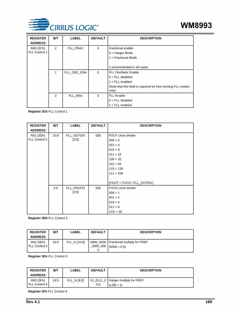
WM8993
Rev 4.1 189
REGISTER
ADDRESS
BIT LABEL DEFAULT DESCRIPTION
R60 (3Ch)
FLL Control 1
2 FLL_FRAC 0 Fractional enable
0 = Integer Mode
1 = Fractional Mode
1 recommended in all cases
1 FLL_OSC_ENA 0 FLL Oscillator Enable
0 = FLL disabled
1 = FLL enabled
(Note that this field is required for free-running FLL modes
only)
0 FLL_ENA 0 FLL Enable
0 = FLL disabled
1 = FLL enabled
Register 3Ch FLL Control 1
REGISTER
ADDRESS
BIT LABEL DEFAULT DESCRIPTION
R61 (3Dh)
FLL Control 2
10:8 FLL_OUTDIV
[2:0]
000 FOUT clock divider
000 = 2
001 = 4
010 = 8
011 = 16
100 = 32
101 = 64
110 = 128
111 = 256
(FOUT = FVCO / FLL_OUTDIV)
2:0 FLL_FRATIO
[2:0]
000 FVCO clock divider
000 = 1
001 = 2
010 = 4
011 = 8
1XX = 16
Register 3Dh FLL Control 2
REGISTER
ADDRESS
BIT LABEL DEFAULT DESCRIPTION
R62 (3Eh)
FLL Control 3
15:0 FLL_K [15:0] 0000_0000
_0000_000
0
Fractional multiply for FREF
(MSB = 0.5)
Register 3Eh FLL Control 3
REGISTER
ADDRESS
BIT LABEL DEFAULT DESCRIPTION
R63 (3Fh)
FLL Control 4
14:5 FLL_N [9:0] 01_0111_0
111
Integer multiply for FREF
(LSB = 1)
Register 3Fh FLL Control 4

WM8993
Rev 4.1 190
REGISTER
ADDRESS
BIT LABEL DEFAULT DESCRIPTION
R64 (40h)
FLL Control 5
12:7 FLL_FRC_NCO
_VAL [5:0]
00_0000 Forces the oscillator value
Valid range is 000000 to 111111
0x19h (011001) = 12MHz approx
(Note that this field is required for free-running FLL modes
only)
6 FLL_FRC_NCO 0 FLL control select
0 = controlled by digital loop (default)
1 = controlled by FLL_FRC_NCO_VAL
(Note that this field is required for free-running FLL modes
only)
4:3 FLL_CLK_REF_
DIV [1:0]
00 FLL Clock Reference Divider
00 = MCLK / 1
01 = MCLK / 2
10 = MCLK / 4
11 = MCLK / 8
MCLK (or other input reference) must be divided down to
<=13.5MHz.
For lower power operation, the reference clock can be
divided down further if desired.
1:0 FLL_CLK_SRC
[1:0]
10 FLL Clock source
00 = MCLK
01 = LRCLK
10 = BCLK
11 = Reserved
Register 40h FLL Control 5
REGISTER
ADDRESS
BIT LABEL DEFAULT DESCRIPTION
R65 (41h)
Clocking 3
13:10 CLK_DCS_DIV
[3:0]
1000 DC Servo Clock Divider
0000 = CLK_SYS
0001 = CLK_SYS / 1.5
0010 = CLK_SYS / 2
0011 = CLK_SYS / 2.5
0100 = CLK_SYS / 3
0101 = CLK_SYS / 4
0110 = CLK_SYS / 5.5
0111 = CLK_SYS / 6
1000 = CLK_SYS / 8
Note - this field is ignored and invalid in Automatic Clocking
Configuration mode.
9:7 SAMPLE_RATE
[2:0]
101 Selects the Sample Rate (fs)
000 = 8kHz
001 = 11.025kHz, 12kHz
010 = 16kHz
011 = 22.05kHz, 24kHz
100 = 32kHz
101 = 44.1kHz, 48kHz
4:1 CLK_SYS_RAT
E [3:0]
0011 Selects the CLK_SYS / fs ratio
0000 = 64
0001 = 128

WM8993
Rev 4.1 191
REGISTER
ADDRESS
BIT LABEL DEFAULT DESCRIPTION
0010 = 192
0011 = 256
0100 = 384
0101 = 512
0110 = 768
0111 = 1024
1000 = 1408
1001 = 1536
0 CLK_DSP_ENA 1 CLK_DSP enable
0 = disabled
1 = enabled
Register 41h Clocking 3
REGISTER
ADDRESS
BIT LABEL DEFAULT DESCRIPTION
R66 (42h)
Clocking 4
9 DAC_DIV4 1 DAC Divide-by-4 select
0 = DAC_DIV
1 = DAC_DIV / 4
Note - this field is ignored and invalid in Automatic Clocking
Configuration mode.
6:1 CLK_256K_DIV
[5:0]
10_1111 256kHz Clock Divider
0d = CLK_SYS
1d = CLK_SYS / 2
2d = CLK_SYS / 3
….
63d = CLK_SYS / 64
Note - this field is ignored and invalid in Automatic Clocking
Configuration mode.
0 SR_MODE 1 Selects Clocking Configuration mode
0 = Automatic
1 = Manual
Register 42h Clocking 4
REGISTER
ADDRESS
BIT LABEL DEFAULT DESCRIPTION
R69 (45h)
Bus Control 1
1 CLK_SYS_ENA 1 CLK_SYS enable
0 = disabled
1 = enabled
Register 45h Bus Control 1
REGISTER
ADDRESS
BIT LABEL DEFAULT DESCRIPTION
R70 (46h)
Write
Sequencer 0
8 WSEQ_ENA 0 Write Sequencer Enable.
0 = Disabled
1 = Enabled
4:0 WSEQ_WRITE_
INDEX [4:0]
0_0000 Sequence Write Index. This is the memory location to which
any updates to R71 and R72 will be copied.
0 to 31 = RAM addresses
Register 46h Write Sequencer 0
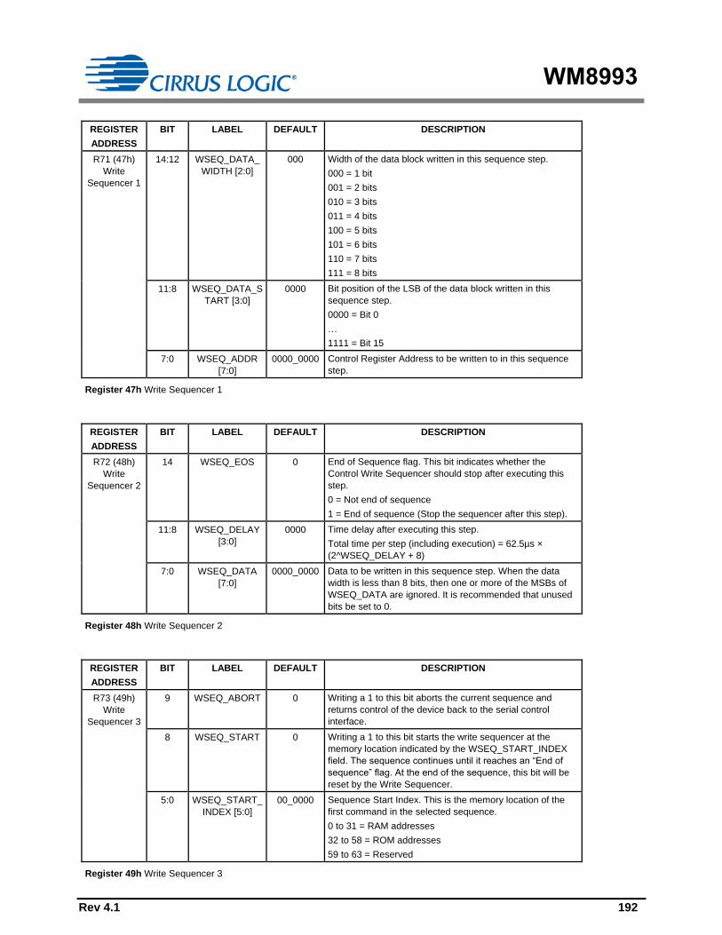
WM8993
Rev 4.1 192
REGISTER
ADDRESS
BIT LABEL DEFAULT DESCRIPTION
R71 (47h)
Write
Sequencer 1
14:12 WSEQ_DATA_
WIDTH [2:0]
000 Width of the data block written in this sequence step.
000 = 1 bit
001 = 2 bits
010 = 3 bits
011 = 4 bits
100 = 5 bits
101 = 6 bits
110 = 7 bits
111 = 8 bits
11:8 WSEQ_DATA_S
TART [3:0]
0000 Bit position of the LSB of the data block written in this
sequence step.
0000 = Bit 0
…
1111 = Bit 15
7:0 WSEQ_ADDR
[7:0]
0000_0000 Control Register Address to be written to in this sequence
step.
Register 47h Write Sequencer 1
REGISTER
ADDRESS
BIT LABEL DEFAULT DESCRIPTION
R72 (48h)
Write
Sequencer 2
14 WSEQ_EOS 0 End of Sequence flag. This bit indicates whether the
Control Write Sequencer should stop after executing this
step.
0 = Not end of sequence
1 = End of sequence (Stop the sequencer after this step).
11:8 WSEQ_DELAY
[3:0]
0000 Time delay after executing this step.
Total time per step (including execution) = 62.5µs ×
(2^WSEQ_DELAY + 8)
7:0 WSEQ_DATA
[7:0]
0000_0000 Data to be written in this sequence step. When the data
width is less than 8 bits, then one or more of the MSBs of
WSEQ_DATA are ignored. It is recommended that unused
bits be set to 0.
Register 48h Write Sequencer 2
REGISTER
ADDRESS
BIT LABEL DEFAULT DESCRIPTION
R73 (49h)
Write
Sequencer 3
9 WSEQ_ABORT 0 Writing a 1 to this bit aborts the current sequence and
returns control of the device back to the serial control
interface.
8 WSEQ_START 0 Writing a 1 to this bit starts the write sequencer at the
memory location indicated by the WSEQ_START_INDEX
field. The sequence continues until it reaches an “End of
sequence” flag. At the end of the sequence, this bit will be
reset by the Write Sequencer.
5:0 WSEQ_START_
INDEX [5:0]
00_0000 Sequence Start Index. This is the memory location of the
first command in the selected sequence.
0 to 31 = RAM addresses
32 to 58 = ROM addresses
59 to 63 = Reserved
Register 49h Write Sequencer 3

WM8993
Rev 4.1 193
REGISTER
ADDRESS
BIT LABEL DEFAULT DESCRIPTION
R74 (4Ah)
Write
Sequencer 4
0 WSEQ_BUSY 0 Sequencer Busy flag (Read Only).
0 = Sequencer idle
1 = Sequencer busy
Note: it is not possible to write to control registers via the
control interface while the Sequencer is Busy.
Register 4Ah Write Sequencer 4
REGISTER
ADDRESS
BIT LABEL DEFAULT DESCRIPTION
R75 (4Bh)
Write
Sequencer 5
5:0 WSEQ_CURRE
NT_INDEX [5:0]
00_0000 Sequence Current Index. This is the location of the most
recently accessed command in the write sequencer
memory.
Register 4Bh Write Sequencer 5
REGISTER
ADDRESS
BIT LABEL DEFAULT DESCRIPTION
R76 (4Ch)
Charge Pump
1
15 CP_ENA 0 Enable charge-pump digits
0 = disable
1 = enable
Note: Default value of R76[14:0] (0x1F25h) must not be
changed when enabling/disabling the Charge Pump
12 Reserved 1 Reserved - do not change
11 Reserved 1 Reserved - do not change
10 Reserved 1 Reserved - do not change
9 Reserved 1 Reserved - do not change
8 Reserved 1 Reserved - do not change
5 Reserved 1 Reserved - do not change
2 Reserved 1 Reserved - do not change
0 Reserved 1 Reserved - do not change
Register 4Ch Charge Pump 1
REGISTER
ADDRESS
BIT LABEL DEFAULT DESCRIPTION
R81 (51h)
Class W 0
0 CP_DYN_PWR 0 Enable dynamic charge pump power control
0 = charge pump controlled by volume register settings
(Class G)
1 = charge pump controlled by real-time audio level (Class
W)
Register 51h Class W 0

WM8993
Rev 4.1 194
REGISTER
ADDRESS
BIT LABEL DEFAULT DESCRIPTION
R84 (54h) DC
Servo 0
13 DCS_TRIG_SIN
GLE_1
0 Writing 1 to this bit selects a single DC offset correction for
HPOUT1R.
In readback, a value of 1 indicates that the DC Servo single
correction is in progress.
12 DCS_TRIG_SIN
GLE_0
0 Writing 1 to this bit selects a single DC offset correction for
HPOUT1L.
In readback, a value of 1 indicates that the DC Servo single
correction is in progress.
9 DCS_TRIG_SE
RIES_1
0 Writing 1 to this bit selects a series of DC offset corrections
for HPOUT1R.
In readback, a value of 1 indicates that the DC Servo DAC
Write correction is in progress.
8 DCS_TRIG_SE
RIES_0
0 Writing 1 to this bit selects a series of DC offset corrections
for HPOUT1L.
In readback, a value of 1 indicates that the DC Servo DAC
Write correction is in progress.
5 DCS_TRIG_STA
RTUP_1
0 Writing 1 to this bit selects Start-Up DC Servo mode for
HPOUT1R.
In readback, a value of 1 indicates that the DC Servo Start-
Up correction is in progress.
4 DCS_TRIG_STA
RTUP_0
0 Writing 1 to this bit selects Start-Up DC Servo mode for
HPOUT1L.
In readback, a value of 1 indicates that the DC Servo Start-
Up correction is in progress.
3 DCS_TRIG_DA
C_WR_1
0 Writing 1 to this bit selects DAC Write DC Servo mode for
HPOUT1R.
In readback, a value of 1 indicates that the DC Servo DAC
Write correction is in progress.
2 DCS_TRIG_DA
C_WR_0
0 Writing 1 to this bit selects DAC Write DC Servo mode for
HPOUT1L.
In readback, a value of 1 indicates that the DC Servo DAC
Write correction is in progress.
1 DCS_ENA_CHA
N_1
0 DC Servo enable for HPOUT1R
0 = disabled
1 = enabled
0 DCS_ENA_CHA
N_0
0 DC Servo enable for HPOUT1L
0 = disabled
1 = enabled
Register 54h DC Servo 0
REGISTER
ADDRESS
BIT LABEL DEFAULT DESCRIPTION
R85 (55h) DC
Servo 1
11:5 DCS_SERIES_
NO_01 [6:0]
010_1010 Number of DC Servo updates to perform in a series event.
0 = 1 updates
1 = 2 updates
...
127 = 128 updates
3:0 DCS_TIMER_P
ERIOD_01 [3:0]
1010 Time between periodic updates. Time is calculated as
0.256s x (2^PERIOD)
0000 = Off
0001 = 0.52s
1010 = 266s (4min 26s)
1111 = 8519s (2hr 22s)

WM8993
Rev 4.1 195
Register 55h DC Servo 1
REGISTER
ADDRESS
BIT LABEL DEFAULT DESCRIPTION
R87 (57h) DC
Servo 3
15:8 DCS_DAC_WR
_VAL_1 [7:0]
0000_0000 DC Offset value for HPOUT1Rin DAC Write DC Servo
mode.
Two’s complement format.
LSB is 0.25mV.
Range is -32mV to +31.75mV
7:0 DCS_DAC_WR
_VAL_0 [7:0]
0000_0000 DC Offset value for HPOUT1Lin DAC Write DC Servo
mode.
Two’s complement format.
LSB is 0.25mV.
Range is -32mV to +31.75mV
Register 57h DC Servo 3
REGISTER
ADDRESS
BIT LABEL DEFAULT DESCRIPTION
R88 (58h) DC
Servo
Readback 0
9:8 DCS_CAL_COM
PLETE [1:0]
00 DC Servo Complete status
0 = DAC Write or Start-Up DC Servo mode not completed.
1 = DAC Write or Start-Up DC Servo mode complete.
Bit [1] = HPOUT1R
Bit [0] = HPOUT1L
5:4 DCS_DAC_WR
_COMPLETE
[1:0]
00 DC Servo DAC Write status
0 = DAC Write DC Servo mode not completed.
1 = DAC Write DC Servo mode complete.
Bit [1] = HPOUT1R
Bit [0] = HPOUT1L
1:0 DCS_STARTUP
_COMPLETE
[1:0]
00 DC Servo Start-Up status
0 = Start-Up DC Servo mode not completed.
1 = Start-Up DC Servo mode complete.
Bit [1] = HPOUT1R
Bit [0] = HPOUT1L
Register 58h DC Servo Readback 0
REGISTER
ADDRESS
BIT LABEL DEFAULT DESCRIPTION
R89 (59h) DC
Servo
Readback 1
7:0 DCS_INTEG_C
HAN_1 [7:0]
0000_0000 Readback value for HPOUT1R.
Two’s complement format.
LSB is 0.25mV.
Range is -32mV to +31.75mV
Register 59h DC Servo Readback 1
REGISTER
ADDRESS
BIT LABEL DEFAULT DESCRIPTION
R90 (5Ah)
DC Servo
Readback 2
7:0 DCS_INTEG_C
HAN_0 [7:0]
0000_0000 Readback value for HPOUT1L.
Two’s complement format.
LSB is 0.25mV.
Range is -32mV to +31.75mV
Register 5Ah DC Servo Readback 2

WM8993
Rev 4.1 196
REGISTER
ADDRESS
BIT LABEL DEFAULT DESCRIPTION
R96 (60h)
Analogue HP
0
8 HPOUT1_AUTO
_PU
1 Enables automatic power-up of HPOUT1 by monitoring
HPOUT1L_ENA and HPOUT1R_ENA
0 = Disabled
1 = Enabled
7 HPOUT1L_RMV
_SHORT
0 Removes HPOUT1L short
0 = HPOUT1L short enabled
1 = HPOUT1L short removed
For normal operation, this bit should be set as the final step
of the HPOUT1L Enable sequence.
6 HPOUT1L_OUT
P
0 Enables HPOUT1L output stage
0 = Disabled
1 = Enabled
For normal operation, this bit should be set to 1 after the
DC offset cancellation has been scheduled.
5 HPOUT1L_DLY 0 Enables HPOUT1L intermediate stage
0 = Disabled
1 = Enabled
For normal operation, this bit should be set to 1 after the
output signal path has been configured, and before DC
offset cancellation is scheduled. This bit should be set with
at least 20us delay after HPOUT1L_ENA.
3 HPOUT1R_RMV
_SHORT
0 Removes HPOUT1R short
0 = HPOUT1R short enabled
1 = HPOUT1R short removed
For normal operation, this bit should be set as the final step
of the HPOUT1R Enable sequence.
2 HPOUT1R_OUT
P
0 Enables HPOUT1R output stage
0 = Disabled
1 = Enabled
For normal operation, this bit should be set to 1 after the
DC offset cancellation has been scheduled.
1 HPOUT1R_DLY 0 Enables HPOUT1R intermediate stage
0 = Disabled
1 = Enabled
For normal operation, this bit should be set to 1 after the
output signal path has been configured, and before DC
offset cancellation is scheduled. This bit should be set with
at least 20us delay after HPOUT1R_ENA.
Register 60h Analogue HP 0
REGISTER
ADDRESS
BIT LABEL DEFAULT DESCRIPTION
R98 (62h)
EQ1
0 EQ_ENA 0 EQ Enable
0 = EQ disabled
1 = EQ enabled
Register 62h EQ1

WM8993
Rev 4.1 197
REGISTER
ADDRESS
BIT LABEL DEFAULT DESCRIPTION
R99 (63h)
EQ2
4:0 EQ_B1_GAIN
[4:0]
0_1100 EQ Band 1 Gain
00000 = -12dB
00001 = -11dB
…
10111 = +11dB
11000 = +12dB
11001 to 11111 Reserved
Register 63h EQ2
REGISTER
ADDRESS
BIT LABEL DEFAULT DESCRIPTION
R100 (64h)
EQ3
4:0 EQ_B2_GAIN
[4:0]
0_1100 EQ Band 2 Gain
00000 = -12dB
00001 = -11dB
…
10111 = +11dB
11000 = +12dB
11001 to 11111 Reserved
Register 64h EQ3
REGISTER
ADDRESS
BIT LABEL DEFAULT DESCRIPTION
R101 (65h)
EQ4
4:0 EQ_B3_GAIN
[4:0]
0_1100 EQ Band 3 Gain
00000 = -12dB
00001 = -11dB
…
10111 = +11dB
11000 = +12dB
11001 to 11111 Reserved
Register 65h EQ4
REGISTER
ADDRESS
BIT LABEL DEFAULT DESCRIPTION
R102 (66h)
EQ5
4:0 EQ_B4_GAIN
[4:0]
0_1100 EQ Band 4 Gain
00000 = -12dB
00001 = -11dB
…
10111 = +11dB
11000 = +12dB
11001 to 11111 Reserved
Register 66h EQ5

WM8993
Rev 4.1 198
REGISTER
ADDRESS
BIT LABEL DEFAULT DESCRIPTION
R103 (67h)
EQ6
4:0 EQ_B5_GAIN
[4:0]
0_1100 EQ Band 5 Gain
00000 = -12dB
00001 = -11dB
…
10111 = +11dB
11000 = +12dB
11001 to 11111 Reserved
Register 67h EQ6
REGISTER
ADDRESS
BIT LABEL DEFAULT DESCRIPTION
R104 (68h)
EQ7
15:0 EQ_B1_A [15:0] 0000_1111
_1100_101
0
EQ Band 1 Coefficient A
Register 68h EQ7
REGISTER
ADDRESS
BIT LABEL DEFAULT DESCRIPTION
R105 (69h)
EQ8
15:0 EQ_B1_B [15:0] 0000_0100
_0000_000
0
EQ Band 1 Coefficient B
Register 69h EQ8
REGISTER
ADDRESS
BIT LABEL DEFAULT DESCRIPTION
R106 (6Ah)
EQ9
15:0 EQ_B1_PG
[15:0]
0000_0000
_1101_100
0
EQ Band 1 Coefficient PG
Register 6Ah EQ9
REGISTER
ADDRESS
BIT LABEL DEFAULT DESCRIPTION
R107 (6Bh)
EQ10
15:0 EQ_B2_A [15:0] 0001_1110
_1011_010
1
EQ Band 2 Coefficient A
Register 6Bh EQ10
REGISTER
ADDRESS
BIT LABEL DEFAULT DESCRIPTION
R108 (6Ch)
EQ11
15:0 EQ_B2_B [15:0] 1111_0001
_0100_010
1
EQ Band 2 Coefficient B
Register 6Ch EQ11

WM8993
Rev 4.1 199
REGISTER
ADDRESS
BIT LABEL DEFAULT DESCRIPTION
R109 (6Dh)
EQ12
15:0 EQ_B2_C [15:0] 0000_1011
_0111_010
1
EQ Band 2 Coefficient C
Register 6Dh EQ12
REGISTER
ADDRESS
BIT LABEL DEFAULT DESCRIPTION
R110 (6Eh)
EQ13
15:0 EQ_B2_PG
[15:0]
0000_0001
_1100_010
1
EQ Band 2 Coefficient PG
Register 6Eh EQ13
REGISTER
ADDRESS
BIT LABEL DEFAULT DESCRIPTION
R111 (6Fh)
EQ14
15:0 EQ_B3_A [15:0] 0001_1100
_0101_100
0
EQ Band 3 Coefficient A
Register 6Fh EQ14
REGISTER
ADDRESS
BIT LABEL DEFAULT DESCRIPTION
R112 (70h)
EQ15
15:0 EQ_B3_B [15:0] 1111_0011
_0111_001
1
EQ Band 3 Coefficient B
Register 70h EQ15
REGISTER
ADDRESS
BIT LABEL DEFAULT DESCRIPTION
R113 (71h)
EQ16
15:0 EQ_B3_C [15:0] 0000_1010
_0101_010
0
EQ Band 3 Coefficient C
Register 71h EQ16
REGISTER
ADDRESS
BIT LABEL DEFAULT DESCRIPTION
R114 (72h)
EQ17
15:0 EQ_B3_PG
[15:0]
0000_0101
_0101_100
0
EQ Band 3 Coefficient PG
Register 72h EQ17
REGISTER
ADDRESS
BIT LABEL DEFAULT DESCRIPTION
R115 (73h)
EQ18
15:0 EQ_B4_A [15:0] 0001_0110
_1000_111
0
EQ Band 4 Coefficient A
Register 73h EQ18

WM8993
Rev 4.1 200
REGISTER
ADDRESS
BIT LABEL DEFAULT DESCRIPTION
R116 (74h)
EQ19
15:0 EQ_B4_B [15:0] 1111_1000
_0010_100
1
EQ Band 4 Coefficient B
Register 74h EQ19
REGISTER
ADDRESS
BIT LABEL DEFAULT DESCRIPTION
R117 (75h)
EQ20
15:0 EQ_B4_C [15:0] 0000_0111
_1010_110
1
EQ Band 4 Coefficient C
Register 75h EQ20
REGISTER
ADDRESS
BIT LABEL DEFAULT DESCRIPTION
R118 (76h)
EQ21
15:0 EQ_B4_PG
[15:0]
0001_0001
_0000_001
1
EQ Band 4 Coefficient PG
Register 76h EQ21
REGISTER
ADDRESS
BIT LABEL DEFAULT DESCRIPTION
R119 (77h)
EQ22
15:0 EQ_B5_A [15:0] 0000_0101
_0110_010
0
EQ Band 5 Coefficient A
Register 77h EQ22
REGISTER
ADDRESS
BIT LABEL DEFAULT DESCRIPTION
R120 (78h)
EQ23
15:0 EQ_B5_B [15:0] 0000_0101
_0101_100
1
EQ Band 5 Coefficient B
Register 78h EQ23
REGISTER
ADDRESS
BIT LABEL DEFAULT DESCRIPTION
R121 (79h)
EQ24
15:0 EQ_B5_PG
[15:0]
0100_0000
_0000_000
0
EQ Band 5 Coefficient PG
Register 79h EQ24

WM8993
Rev 4.1 201
REGISTER
ADDRESS
BIT LABEL DEFAULT DESCRIPTION
R122 (7Ah)
Digital Pulls
7 MCLK_PU 0 MCLK pull-up resistor enable
0 = pull-up disabled
1 = pull-up enabled
6 MCLK_PD 0 MCLK pull-down resistor enable
0 = pull-down disabled
1 = pull-down enabled
5 DACDAT_PU 0 DACDAT pull-up resistor enable
0 = pull-up disabled
1 = pull-up enabled
4 DACDAT_PD 0 DACDAT pull-down resistor enable
0 = pull-down disabled
1 = pull-down enabled
3 LRCLK_PU 0 LRCLK pull-up resistor enable
0 = pull-up disabled
1 = pull-up enabled
2 LRCLK_PD 0 LRCLK pull-down resistor enable
0 = pull-down disabled
1 = pull-down enabled
1 BCLK_PU 0 BCLK pull-up resistor enable
0 = pull-up disabled
1 = pull-up enabled
0 BCLK_PD 0 BCLK pull-down resistor enable
0 = pull-down disabled
1 = pull-down enabled
Register 7Ah Digital Pulls
REGISTER
ADDRESS
BIT LABEL DEFAULT DESCRIPTION
R123 (7Bh)
DRC Control
1
15 DRC_ENA 0 DRC enable
0 = disabled
1 = enabled
14 DRC_DAC_PAT
H
0 DRC path select
0 = ADC path
1 = DAC path
11 DRC_SMOOTH
_ENA
1 Gain smoothing enable
0 = disabled
1 = enabled
10 DRC_QR_ENA 1 Quick release enable
0 = disabled
1 = enabled
9 DRC_ANTICLIP
_ENA
1 Anti-clip enable
0 = disabled
1 = enabled
8 DRC_HYST_EN
A
1 Gain smoothing hysteresis enable
0 = disabled
1 = enabled
5:4 DRC_THRESH_
HYST [1:0]
00 Gain smoothing hysteresis threshold
00 = Low
01 = Medium (recommended)
10 = High

WM8993
Rev 4.1 202
REGISTER
ADDRESS
BIT LABEL DEFAULT DESCRIPTION
11 = Reserved
3:2 DRC_MINGAIN
[1:0]
10 Minimum gain the DRC can use to attenuate audio signals
00 = 0dB (default)
01 = -6dB
10 = -12dB
11 = -18dB
1:0 DRC_MAXGAIN
[1:0]
00 Maximum gain the DRC can use to boost audio signals
00 = 12dB
01 = 18dB (default)
10 = 24dB
11 = 36dB
Register 7Bh DRC Control 1
REGISTER
ADDRESS
BIT LABEL DEFAULT DESCRIPTION
R124 (7Ch)
DRC Control
2
15:12 DRC_ATTACK_
RATE [3:0]
0000 Gain attack rate (seconds/6dB)
0000 = Reserved
0001 = 181us
0010 = 363us
0011 = 726us
0100 = 1.45ms
0101 = 2.9ms
0110 = 5.8ms
0111 = 11.6ms
1000 = 23.2ms
1001 = 46.4ms
1010 = 92.8ms
1011 = 185.6ms
1100-1111 = Reserved
11:8 DRC_DECAY_R
ATE [3:0]
0000 Gain decay rate (seconds/6dB)
0000 = 186ms
0001 = 372ms
0010 = 743ms
0011 = 1.49s
0100 = 2.97s
0101 = 5.94s
0110 = 11.89s
0111 = 23.78s
1000 = 47.56s
1001-1111 = Reserved
7:2 DRC_THRESH_
COMP [5:0]
00_0000 Compressor threshold T (dB)
000000 = 0dB
000001 = -0.75dB
000010 = -1.5dB
… (-0.75dB steps)
111100 = -45dB
111101 = Reserved
11111X = Reserved
Register 7Ch DRC Control 2

WM8993
Rev 4.1 203
REGISTER
ADDRESS
BIT LABEL DEFAULT DESCRIPTION
R125 (7Dh)
DRC Control
3
15:11 DRC_AMP_CO
MP [4:0]
0_0000 Compressor amplitude at threshold YT (dB)
00000 = 0dB
00001 = -0.75dB
00010 = -1.5dB
… (-0.75dB steps)
11110 = -22.5dB
11111 = Reserved
10:8 DRC_R0_SLOP
E_COMP [2:0]
000 Compressor slope R0
000 = 1 (no compression)
001 = 1/2
010 = 1/4
011 = 1/8
100 = 1/16
101 = 0
110 = Reserved
111 = Reserved
7 DRC_FF_DELA
Y
1 Feed-forward delay for anti-clip feature
0 = 5 samples
1 = 9 samples
Time delay can be calculated as 5/fs or 9/ fs, where fs is the
sample rate.
3:2 DRC_THRESH_
QR [1:0]
00 Quick release crest factor threshold
00 = 12dB
01 = 18dB (default)
10 = 24dB
11 = 30dB
1:0 DRC_RATE_QR
[1:0]
00 Quick release decay rate (seconds/6dB)
00 = 0.725ms (default)
01 = 1.45ms
10 = 5.8ms
11 = Reserved
Register 7Dh DRC Control 3
REGISTER
ADDRESS
BIT LABEL DEFAULT DESCRIPTION
R126 (7Eh)
DRC Control
4
15:13 DRC_R1_SLOP
E_COMP [2:0]
000 Compressor slope R1
000 = 1 (no compression)
001 = 1/2
010 = 1/4
011 = 1/8
100 = 0
101 = Reserved
11X = Reserved
12:8 DRC_STARTUP
_GAIN [4:0]
0_0000 Initial gain at DRC startup
00000 = -18dB
00001 = -15dB
00010 = -12dB
00011 = -9dB
00100 = -6dB
00101 = -3dB
00110 = 0dB (default)
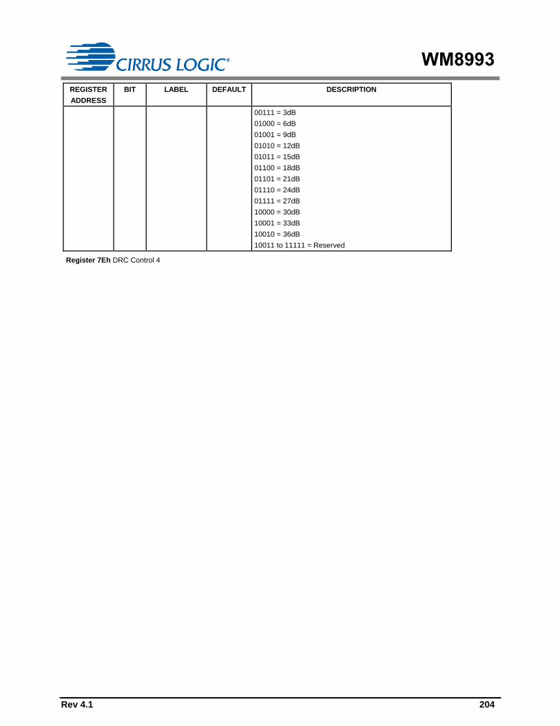
WM8993
Rev 4.1 204
REGISTER
ADDRESS
BIT LABEL DEFAULT DESCRIPTION
00111 = 3dB
01000 = 6dB
01001 = 9dB
01010 = 12dB
01011 = 15dB
01100 = 18dB
01101 = 21dB
01110 = 24dB
01111 = 27dB
10000 = 30dB
10001 = 33dB
10010 = 36dB
10011 to 11111 = Reserved
Register 7Eh DRC Control 4

WM8993
Rev 4.1 205
DIGITAL FILTER CHARACTERISTICS
PARAMETER TEST CONDITIONS MIN TYP MAX UNIT
ADC Filter
Passband +/- 0.05dB 0 0.454 fs
-6dB 0.5 fs
Passband Ripple +/- 0.05 dB
Stopband 0.546 fs
Stopband Attenuation f > 0.546 fs -60 dB
Group delay 2 ms
DAC Normal Filter
Passband +/- 0.05dB 0 0.454 fs
-6dB 0.5 fs
Passband Ripple 0.454 fs +/- 0.03 dB
Stopband 0.546 fs
Stopband Attenuation f > 0.546 fs -50 dB
Group delay 2 ms
DAC Sloping Stopband Filter
Passband +/- 0.03dB 0 0.25 fs
+/- 1dB 0.25 fs 0.454 fs
-6dB 0.5 fs
Passband Ripple 0.25 fs +/- 0.03 dB
Stopband 1 0.546 fs 0.7 fs
Stopband 1 Attenuation f > 0.546 fs -60 dB
Stopband 2 0.7 fs 1.4 fs
Stopband 2 Attenuation f > 0.7 fs -85 dB
Stopband 3 1.4 fs
Stopband 3 Attenuation f > 1.4 fs -55 dB
Group delay 2 ms
TERMINOLOGY
1. Stop Band Attenuation (dB) – the degree to which the frequency spectrum is attenuated (outside audio band)
2. Pass-band Ripple – any variation of the frequency response in the pass-band region

WM8993
Rev 4.1 206
ADC FILTER RESPONSES
Figure 71 ADC Digital Filter Frequency Response Figure 72 ADC Digital Filter Ripple
ADC HIGH PASS FILTER RESPONSES
hpf_response.res MAGNITUDE(dB) hpf_response2.res MAGNITUDE(dB)
hpf_response2.res#1 MAGNITUDE(dB)
2 5.0248 12.624 31.716 79.683 200.19 502.96 1.2636k 3.1747k 7.9761k 20.039k
-83.352
-75.017
-66.682
-58.347
-50.012
-41.677
-33.342
-25.007
-16.672
-8.3373
-2.3338m
Figure 73 ADC Digital High Pass Filter Frequency
Response (48kHz, Hi-Fi Mode, ADC_HPF_CUT[1:0]=00)
Figure 74 ADC Digital High Pass Filter Ripple (48kHz,
Voice Mode, ADC_HPF_CUT=01, 10 and 11)
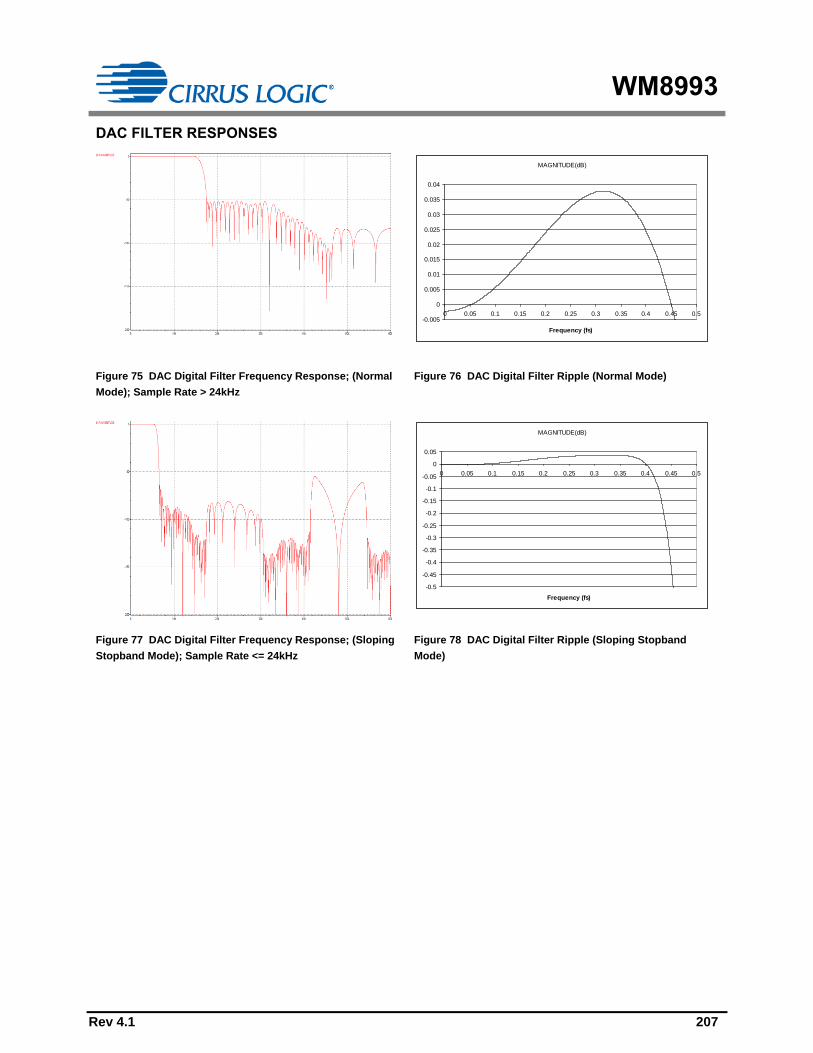
WM8993
Rev 4.1 207
DAC FILTER RESPONSES
MAGNITUDE(dB)
-0.005
0
0.005
0.01
0.015
0.02
0.025
0.03
0.035
0.04
0 0.05 0.1 0.15 0.2 0.25 0.3 0.35 0.4 0.45 0.5
Frequency (fs)
Figure 75 DAC Digital Filter Frequency Response; (Normal
Mode); Sample Rate > 24kHz
Figure 76 DAC Digital Filter Ripple (Normal Mode)
MAGNITUDE(dB)
-0.5
-0.45
-0.4
-0.35
-0.3
-0.25
-0.2
-0.15
-0.1
-0.05
0
0.05
0 0.05 0.1 0.15 0.2 0.25 0.3 0.35 0.4 0.45 0.5
Frequency (fs)
Figure 77 DAC Digital Filter Frequency Response; (Sloping
Stopband Mode); Sample Rate <= 24kHz
Figure 78 DAC Digital Filter Ripple (Sloping Stopband
Mode)

WM8993
Rev 4.1 208
DE-EMPHASIS FILTER RESPONSES
MAGNITUDE(dB)
-10
-9
-8
-7
-6
-5
-4
-3
-2
-1
0
0 5000 10000 15000 20000
Frequency (Hz)
MAGNITUDE(dB)
-0.15
-0.1
-0.05
0
0.05
0.1
0.15
0.2
0.25
0.3
0 2000 4000 6000 8000 10000 12000 14000 16000 18000
Frequency (Hz)
Figure 79 De-Emphasis Digital Filter Response (32kHz) Figure 80 De-Emphasis Error (32kHz)
MAGNITUDE(dB)
-10
-9
-8
-7
-6
-5
-4
-3
-2
-1
0
0 5000 10000 15000 20000 25000
Frequency (Hz)
MAGNITUDE(dB)
-0.1
-0.05
0
0.05
0.1
0.15
0.2
0 5000 10000 15000 20000 25000
Frequency (Hz)
Figure 81 De-Emphasis Digital Filter Response (44.1kHz) Figure 82 De-Emphasis Error (44.1kHz)
MAGNITUDE(dB)
-12
-10
-8
-6
-4
-2
0
0 5000 10000 15000 20000 25000 30000
Frequency (Hz)
MAGNITUDE(dB)
-0.15
-0.1
-0.05
0
0.05
0.1
0.15
0 5000 10000 15000 20000 25000 30000
Frequency (Hz)
Figure 83 De-Emphasis Digital Filter Response (48kHz) Figure 84 De-Emphasis Error (48kHz)
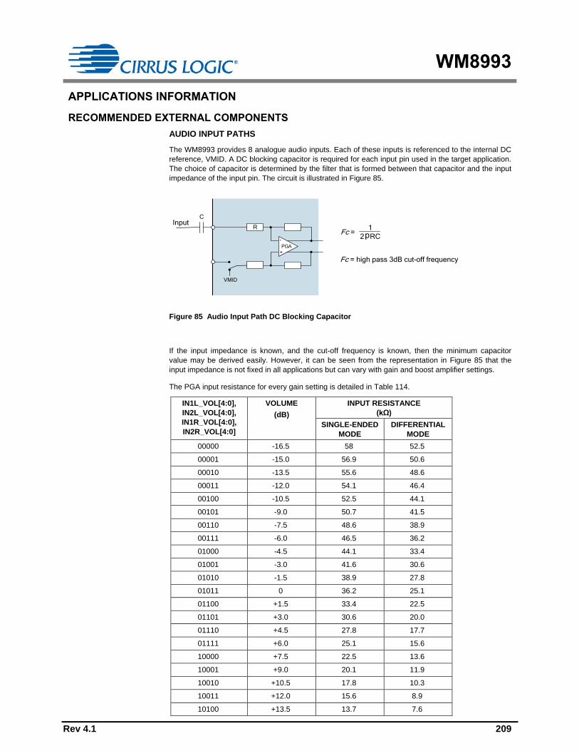
WM8993
Rev 4.1 209
APPLICATIONS INFORMATION
RECOMMENDED EXTERNAL COMPONENTS
AUDIO INPUT PATHS
The WM8993 provides 8 analogue audio inputs. Each of these inputs is referenced to the internal DC
reference, VMID. A DC blocking capacitor is required for each input pin used in the target application.
The choice of capacitor is determined by the filter that is formed between that capacitor and the input
impedance of the input pin. The circuit is illustrated in Figure 85.
+
-
PGA
VMID
InputC
R
Fc = high pass 3dB cut-off frequency
Fc = 1
2 RCp
Figure 85 Audio Input Path DC Blocking Capacitor
If the input impedance is known, and the cut-off frequency is known, then the minimum capacitor
value may be derived easily. However, it can be seen from the representation in Figure 85 that the
input impedance is not fixed in all applications but can vary with gain and boost amplifier settings.
The PGA input resistance for every gain setting is detailed in Table 114.
IN1L_VOL[4:0],
IN2L_VOL[4:0],
IN1R_VOL[4:0],
IN2R_VOL[4:0]
VOLUME
(dB)
INPUT RESISTANCE
(kΩ)
SINGLE-ENDED
MODE
DIFFERENTIAL
MODE
00000 -16.5 58 52.5
00001 -15.0 56.9 50.6
00010 -13.5 55.6 48.6
00011 -12.0 54.1 46.4
00100 -10.5 52.5 44.1
00101 -9.0 50.7 41.5
00110 -7.5 48.6 38.9
00111 -6.0 46.5 36.2
01000 -4.5 44.1 33.4
01001 -3.0 41.6 30.6
01010 -1.5 38.9 27.8
01011 0 36.2 25.1
01100 +1.5 33.4 22.5
01101 +3.0 30.6 20.0
01110 +4.5 27.8 17.7
01111 +6.0 25.1 15.6
10000 +7.5 22.5 13.6
10001 +9.0 20.1 11.9
10010 +10.5 17.8 10.3
10011 +12.0 15.6 8.9
10100 +13.5 13.7 7.6

WM8993
Rev 4.1 210
10101 +15.0 11.9 6.5
10110 +16.5 10.3 5.6
10111 +18.0 8.9 4.8
11000 +19.5 7.7 4.1
11001 +21.0 6.6 3.5
11010 +22.5 5.6 2.9
11011 +24.0 4.8 2.5
11100 +25.5 4.1 2.1
11101 +27.0 3.5 1.8
11110 +28.5 2.9 1.5
11111 +30.0 2.5 1.3
Table 114 PGA Input Pin Resistance
The appropriate input capacitor may be selected using the PGA input resistance data provided in
Table 114, depending on the required PGA gain setting(s).
The choice of capacitor for a 20Hz cut-off frequency is shown in Table 115 for a selection of typical
input impedance conditions.
INPUT IMPEDANCE MINIMUM CAPACITANCE
FOR 20HZ PASS BAND
2k 4 F
15k 0.5 F
30k 0.27 F
60k 0.13 F
Table 115 Audio Input DC Blocking Capacitors
Using the figures in Table 115, it follows that a 1F capacitance for all input connections will give good
results in most cases. Tantalum electrolytic capacitors are particularly suitable as they offer high
stability in a small package size.
Ceramic equivalents are a cost effective alternative to the superior tantalum packages, but care must
be taken to ensure the desired capacitance is maintained at the AVDD1 operating voltage. Also,
ceramic capacitors may show microphonic effects, where vibrations and mechanical conditions give
rise to electrical signals. This is particularly problematic for microphone input paths where a large
signal gain is required.
A single capacitor is required for a line input or single-ended microphone connection. In the case of a
differential microphone connection, a DC blocking capacitor is required on both input pins.

WM8993
Rev 4.1 211
HEADPHONE OUTPUT PATH
The headphone output on WM8993 is ground referenced and therefore does not require the large,
expensive capacitors necessary for VMID reference solutions. For best audio performance, it is
recommended to connect a zobel network to the audio output pins. This network should comprise of a
100nF capacitor and 20ohm resistor in series with each other (see “Analogue Outputs” section).
These components have the effect of dampening high frequency oscillations or instabilities that can
arise outside the audio band under certain conditions. Possible sources of these instabilities include
the inductive load of a headphone coil or an active load in the form of an external line amplifier.
EARPIECE DRIVER OUTPUT PATH
The earpiece driver on HPOUT2P and HPOUTN is designed as a 32ohm BTL speaker driver. The
outputs are referenced to the internal DC reference VMID, but direct connection to the speaker is
possible because of the BTL configuration. There is no requirement for DC blocking capacitors.
LINE OUTPUT PATHS
The WM8993 provides four line outputs (LINEOUT1P, LINEOUT1N, LINEOUT2P and LINEOUT2N).
Each of these outputs is referenced to the internal DC reference, VMID. In any the case where a line
output is used in a single-ended configuration (i.e. referenced to AGND), a DC blocking capacitor will
be required in order to remove the DC bias. In the case where a pair of line outputs is configured as a
BTL differential pair, then the DC blocking capacitor should be omitted.
The choice of capacitor is determined from the filter that is formed between the capacitor and the load
impedance – see Figure 86.
Fc = high pass 3dB cut-off frequency
Fc = 1
2 RCp
Output C
R
Figure 86 Line Output Path Components
LOAD IMPEDANCE MINIMUM CAPACITANCE
FOR 20HZ PASS BAND
10k 0.8 F
47k 0.17 F
Table 116 Line Output Frequency Cut-Off
Using the figures in Table 116, it follows that that a 1F capacitance would be a suitable choice for a
line load. Tantalum electrolytic capacitors are again particularly suitable but ceramic equivalents are a
cost effective alternative. Care must be taken to ensure the desired capacitance is maintained at the
appropriate operating voltage.

WM8993
Rev 4.1 212
POWER SUPPLY DECOUPLING
Electrical coupling exists particularly in digital logic systems where switching in one sub-system
causes fluctuations on the power supply. This effect occurs because the inductance of the power
supply acts in opposition to the changes in current flow that are caused by the logic switching. The
resultant variations (or ‘spikes’) in the power supply voltage can cause malfunctions and unintentional
behavior in other components. A decoupling (or ‘bypass’) capacitor can be used as an energy storage
component which will provide power to the decoupled circuit for the duration of these power supply
variations, protecting it from malfunctions that could otherwise arise.
Coupling also occurs in a lower frequency form when ripple is present on the power supply rail caused
by changes in the load current or by limitations of the power supply regulation method. In audio
components such as the WM8993, these variations can alter the performance of the signal path,
leading to degradation in signal quality. A decoupling (or ‘bypass’) capacitor can be used to filter these
effects, by presenting the ripple voltage with a low impedance path that does not affect the circuit to
be decoupled.
These coupling effects are addressed by placing a capacitor between the supply rail and the
corresponding ground reference. In the case of systems comprising multiple power supply rails,
decoupling should be provided on each rail.
The recommended power supply decoupling capacitors for WM8993 are listed below in Table 117.
POWER SUPPLY DECOUPLING CAPACITOR
DCVDD, DBVDD, AVDD2 0.1F ceramic
AVDD1, SPKVDD 0.1F ceramic (see Note)
CPVDD 4.7F ceramic
VMIDC 4.7F ceramic
Table 117 Power Supply Decoupling Capacitors
Note: 0.1F is required with 4.7F a guide to the total required power rail capacitance, including that
at the regulator output.
All decoupling capacitors should be placed as close as possible to the WM8993 device. The
connection between AGND, the AVDD1 decoupling capacitor and the main system ground should be
made at a single point as close as possible to the AGND ball of the WM8993.
The VMID capacitor is not, technically, a decoupling capacitor. However, it does serve a similar
purpose in filtering noise on the VMID reference. The connection between AGND, the VMID
decoupling capacitor and the main system ground should be made at a single point as close as
possible to the AGND ball of the WM8993.
Due to the wide tolerance of many types of ceramic capacitors, care must be taken to ensure that the
selected components provide the required capacitance across the required temperature and voltage
ranges in the intended application. For most application the use of ceramic capacitors with capacitor
dielectric X5R is recommended.

WM8993
Rev 4.1 213
CHARGE PUMP COMPONENTS
A fly-back capacitor is required between the CPCA and CPCB pins. The required capacitance is
2.2µF at 2V.
A decoupling capacitor is required on CPVOUTP and CPVOUTN; the recommended value is 2.2µF at
2V.
The positioning of the Charge Pump capacitors is important, particularly the fly-back capacitor. These
capacitors should be placed as close as possible to the WM8994.
Due to the wide tolerance of many types of ceramic capacitors, care must be taken to ensure that the
selected components provide the required capacitance across the required temperature and voltage
ranges in the intended application. For most application the use of ceramic capacitors with capacitor
dielectric X5R is recommended.
MICROPHONE BIAS CIRCUIT
The WM8993 is designed to interface easily with up to four microphones. These may be connected in
single-ended or differential configurations. The single-ended method allows greater capability for the
connection of multiple audio sources simultaneously, whilst the differential method provides better
performance due to its rejection of common-mode noise.
In either configuration, the microphone requires a bias current (electret condenser microphones) or
voltage supply (silicon microphones), which can be provided by MICBIAS1 or MICBIAS2. These are
generated by identical output-compensated amplifiers, which require an external capacitor in order to
guarantee accuracy and stability. The recommended capacitance is 4.7F, although it may be
possible to reduce this to 1F if the analogue supply (AVDD1) is not too noisy. A ceramic type is a
suitable choice here, providing that care is taken to choose a component that exhibits this capacitance
at the intended MICBIAS voltage.
Note that the MICBIAS voltage may be adjusted using register control to suit the requirements of the
microphone. Also note the WM8993 supports a maximum current of 2.4mA per MICBIAS pin. If more
than one microphone is connected to a single MICBIAS pin, the combined current of these must not
exceed 2.4mA.
A current-limiting resistor is also required when using an electret condenser microphone (ECM). The
resistance should be chosen according to the minimum operating impedance of the microphone and
MICBIAS voltage so that the maximum bias current of the WM8993 is not exceeded. Cirrus Logic
recommends a 2.2k current limiting resistor as it provides compatibility with a wide range of
microphone models.
Figure 87 illustrates the recommended single-ended and differential microphone connections for the
WM8993.
MIC
To
input
mixers
+
-
PGA
Line Input
VMID
IN1LN,
IN2LN,
IN1RN,
IN2RN
IN1LP,
IN2LP,
IN1RP,
IN2RP
MICBIAS1/2
C
2k2
4.7uF
AGND
MICTo
input
mixers
+
-
PGA
Line Input
VMID
IN1LN,
IN2LN,
IN1RN,
IN2RN
IN1LP,
IN2LP,
IN1RP,
IN2RP
MICBIAS1/2
C
2k2
C
4.7uF
AGND
Figure 87 Single-Ended and Differential Microphone Connections

WM8993
Rev 4.1 214
CLASS D SPEAKER CONNECTIONS
The WM8993 incorporates two Class D/AB 1W speaker drivers. By default, the speaker drivers
operate in Class D mode, which offers high amplifier efficiency at large signal levels. As the Class D
output is a pulse width modulated signal, the choice of speakers and tracking of signals is critical for
ensuring good performance and reducing EMI in this mode.
The efficiency of the speaker drivers is affected by the series resistance between the WM8993 and
the speaker (e.g. PCB track loss and inductor ESR) as shown in Figure 88. This resistance should be
as low as possible to maximise efficiency.
GND
Losses due to resistance between WM8993 and speaker (e.g. inductor ESR)
This resistance must be minimised in order to maximise efficiency.
Switching
LossesClass D
output
SPKVDD
SPKVDD/2
Figure 88 Speaker Connection Losses
The Class D output requires external filtering in order to recreate the audio signal. This may be
implemented using a 2nd order LC or 1st order RC filter, or else may be achieved by using a
loudspeaker whose internal inductance provides the required filter response. An LC or RC filter should
be used if the loudspeaker characteristics are unknown or unsuitable, or if the length of the
loudspeaker connection is likely to lead to EMI problems.
In applications where it is necessary to provide Class D filter components, a 2nd order LC filter is the
recommended solution as it provides more attenuation at higher frequencies and minimises power
dissipated in the filter when compared to a first order RC filter (lower ESR). This maximises both
rejection of unwanted switching frequencies and overall speaker efficiency. A suitable implementation
is illustrated in Figure 89.
WM8993C = 3mF
L = 22mHSPKP
SPKN Fc = low pass 3dB
cut-off frequency
Fc =1
2 p LC
Figure 89 Class D Output Filter Components

WM8993
Rev 4.1 215
A simple equivalent circuit of a loudspeaker consists of a serially connected resistor and inductor, as shown in
Figure 90. This circuit provides a low pass filter for the speaker output. If the loudspeaker characteristics are
suitable, then the loudspeaker itself can be used in place of the filter components described earlier. This is
known as ‘filterless’ operation.
Fc =R
2 p L
WM8993 RL
SPKP
SPKNFc = low pass 3dB cut-off frequency
Figure 90 Speaker Equivalent Circuit for Filterless Operation
For filterless Class D operation, it is important to ensure that a speaker with suitable inductance is
chosen. For example, if we know the speaker impedance is 8Ω and the desired cut-off frequency is
20kHz, then the optimum speaker inductance may be calculated as:
L = = = 64HR
2 p Fc
8
2 p * 20kHz
8 loudspeakers typically have an inductance in the range 20H to 100H, however, it should be
noted that a loudspeaker inductance will not be constant across the relevant frequencies for Class D
operation (up to and beyond the Class D switching frequency). Care should be taken to ensure that
the cut-off frequency of the loudspeaker’s filtering is low enough to suppress the high frequency
energy of the Class D switching and, in so doing, to prevent speaker damage. The Class D outputs of
the WM8993 operate at much higher frequencies than is recommended for most speakers and it must
be ensured that the cut-off frequency is low enough to protect the speaker.

WM8993
Rev 4.1 216
RECOMMENDED EXTERNAL COMPONENTS DIAGRAM
Figure 91 and Figure 92 below provide a summary of recommended external components for
WM8993. Note that these diagrams do not include any components that are specific to the end
application e.g. they do not include filtering on the speaker outputs (assume filterless class D
operation), RF decoupling, or RF filtering for pins which connect to the external world i.e. headphone
or speaker outputs.
WM8993
AVDD1 AGND
DCVDD
CPVDD
AVDD2
DBVDD
SPKVDD
DGND
CPGND
SPKGND
MCLK
DACDAT
LRCLK
BCLK
ADCDAT
SDAT
SCLK
GPIO1
IN1LN
IN1RN
IN2LP/VRXN
IN2LN/GI7
IN1RP
IN1LP
IN2RN/GI8
IN2RP/VRXP
MICBIAS1
VMIDC
MICBIAS2
HPOUT2N
HPOUT2P
HPOUT1L
HPOUT1FB
HPOUT1R
LINEOUT1N
LINEOUT2P
LINEOUT2N
LINEOUT1P
LINEOUTFB
SPKOUTLN
SPKOUTRP
SPKOUTRN
SPKOUTLP
CPFB1
CPVOUTP
CPVOUTN
CPFB2
FM Radio
2.2F
2.2F 2.2F
Left
Loudspeaker
8
Right
Loudspeaker
8
Earpiece
Speaker
32
4.7F 4.7F 4.7F
MICBIAS1
Headset
16
Differential Line-out
to Voice CODEC
1F
1F
1F
1F
4.7F
Stereo Line-out
0.1F0.1F4.7F0.1F0.1F0.1F
3.0V Vbatt 1.8V
Master Clock and
Audio Interface
Control Interface
Differential
RXVOICE Input from
Voice CODEC
1F
1F
1F
1F
1F
1F
1F
1F
Differential MIC Input
from Headset MIC
Handset MIC
2.2k
2.2k
MICBIAS1
GPIO
0.1F 0.1F
20R 20RSPKMONO
(Note: HPOUT1FB ground
connection close to headset jack)
Figure 91 Recommended External Components Diagram – 1W Stereo Mode
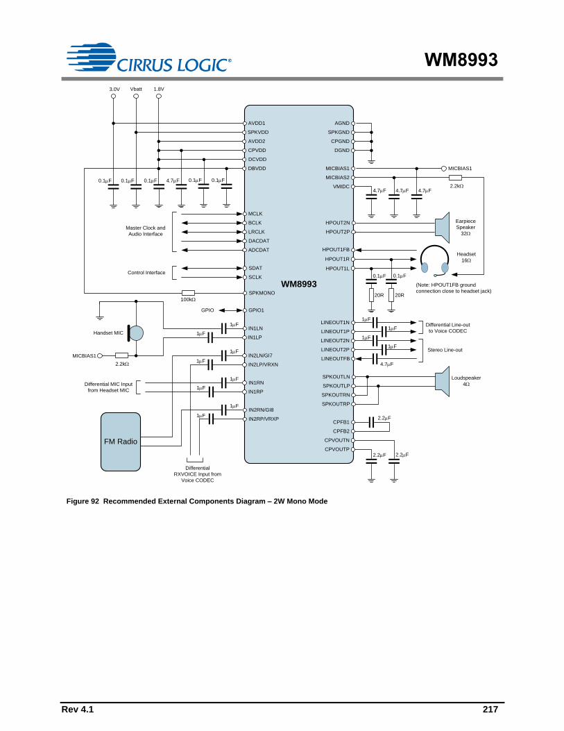
WM8993
Rev 4.1 217
WM8993
AVDD1 AGND
DCVDD
CPVDD
AVDD2
DBVDD
SPKVDD
DGND
CPGND
SPKGND
MCLK
DACDAT
LRCLK
BCLK
ADCDAT
SDAT
SCLK
GPIO1
IN1LN
IN1RN
IN2LP/VRXN
IN2LN/GI7
IN1RP
IN1LP
IN2RN/GI8
IN2RP/VRXP
MICBIAS1
VMIDC
MICBIAS2
HPOUT2N
HPOUT2P
HPOUT1L
HPOUT1FB
HPOUT1R
LINEOUT1N
LINEOUT2P
LINEOUT2N
LINEOUT1P
LINEOUTFB
SPKOUTLN
SPKOUTRP
SPKOUTRN
SPKOUTLP
CPFB1
CPVOUTP
CPVOUTN
CPFB2
FM Radio
2.2F
2.2F 2.2F
Loudspeaker
4
Earpiece
Speaker
32
4.7F 4.7F 4.7F
MICBIAS1
Headset
16
Differential Line-out
to Voice CODEC
1F
1F
1F
1F
4.7F
Stereo Line-out
0.1F0.1F4.7F0.1F0.1F0.1F
3.0V Vbatt 1.8V
Master Clock and
Audio Interface
Control Interface
Differential
RXVOICE Input from
Voice CODEC
1F
1F
1F
1F
1F
1F
1F
1F
Differential MIC Input
from Headset MIC
Handset MIC
2.2k
2.2k
MICBIAS1
GPIO
0.1F 0.1F
20R 20RSPKMONO
100k
(Note: HPOUT1FB ground
connection close to headset jack)
Figure 92 Recommended External Components Diagram – 2W Mono Mode

WM8993
Rev 4.1 218
PCB LAYOUT CONSIDERATIONS
Poor PCB layout will degrade the performance and be a contributory factor in EMI, ground bounce
and resistive voltage losses. All external components should be placed as close to the WM8993
device as possible, with current loop areas kept as small as possible. Specific factors relating to Class
D loudspeaker connection are detailed below.
CLASS D LOUDSPEAKER CONNECTION
Long, exposed PCB tracks or connection wires will emit EMI. The distance between the WM8993 and
the loudspeaker should therefore be kept as short as possible. Where speakers are connected to the
PCB via a cable form, it is recommended that a shielded twisted pair cable is used. The shield should
be connected to the main system, with care taken to ensure ground loops are avoided.
Further reduction in EMI can be achieved using PCB ground (or VDD) planes and also by using
passive LC components to filter the Class D switching waveform. When passive filtering is used, low
ESR components should be chosen in order to minimise the series resistance between the WM8993
and the speaker, maximising the power efficiency.
LC passive filtering will usually be effective at reducing EMI at frequencies up to around 30MHz. To
reduce emissions at higher frequencies, ferrite beads can also be used. These should be positioned
as close to the device as possible.
These techniques for EMI reduction are illustrated in Figure 93.
WM8993
SPKP
SPKNEMI
WM8993
SPKP
SPKN
WM8993
SPKP
SPKN
LOW ESR
LOW ESR
WM8993
SPKP
SPKN
WM8993
SPKP
SPKN
Long, exposed tracks emit EMI
Short connection wires will reduce EMI emission
Shielding using PCB ground (or VDD) planes
will reduce EMI emission
LC filtering will reduce EMI emission
up to around 30MHz
Ferrite beads will reduce EMI emission
at frequencies above 30MHz.
Figure 93 EMI Reduction Techniques

WM8993
Rev 4.1 219
PACKAGE DIMENSIONS
DM060.DB: 48 BALL W-CSP PACKAGE 3.65 X 3.55 X 0.546mm BODY, 0.50 mm BALL PITCH
A1
CORNER
TOP VIEW
E
Z0.102 X
D
5
4
DETAIL 2
DETAIL 2
A
A2
2
Z0.102 X
A1
Zbbb
Z
1
SOLDER BALL
E1
A
D1
DETAIL 1
D
C
B
G
F
E
e
e
BOTTOM VIEW
16 5 4 3 2
6
f1
f2
G
h
NOTES:
1. PRIMARY DATUM -Z- AND SEATING PLANE ARE DEFINED BY THE SPHERICAL CROWNS OF THE SOLDER BALLS.
2. THIS DIMENSION INCLUDES STAND-OFF HEIGHT ‘A1’ AND BACKSIDE COATING.
3. A1 CORNER IS IDENTIFIED BY INK/LASER MARK ON TOP PACKAGE.
4. BILATERAL TOLERANCE ZONE IS APPLIED TO EACH SIDE OF THE PACKAGE BODY.
5. ‘e’ REPRESENTS THE BASIC SOLDER BALL GRID PITCH.
6. THIS DRAWING IS SUBJECT TO CHANGE WITHOUT NOTICE.
7. FOLLOWS JEDEC DESIGN GUIDE MO-211-C.
A1 0.207
D
D1
E
E1
e
3.000 BSC
3.550
0.325 BSC
3.000 BSC
0.500 BSC
3.650
Dimensions (mm)Symbols
MIN NOM MAX NOTE
A 0.546
A2 0.265 0.280 0.295
5
f1
0.5860.506
0.244 0.281
g 0.0220.019 0.025
h 0.314 BSC
7
0.275 BSCf2
3.620
3.520
3.680
3.580

WM8993
Rev 4.1 220
IMPORTANT NOTICE
Contacting Cirrus Logic Support For all product questions and inquiries, contact a Cirrus Logic Sales Representative.
To find one nearest you, go to www.cirrus.com.
For the purposes of our terms and conditions of sale, "Preliminary" or "Advanced" datasheets are non-final datasheets that include
but are not limited to datasheets marked as “Target”, “Advance”, “Product Preview”, “Preliminary Technical Data” and/or “Pre-
production.” Products provided with any such datasheet are therefore subject to relevant terms and conditions associated with
"Preliminary" or "Advanced" designations. The products and services of Cirrus Logic International (UK) Limited; Cirrus Logic, Inc.;
and other companies in the Cirrus Logic group (collectively either “Cirrus Logic” or “Cirrus”) are sold subject to Cirrus Logic’s terms
and conditions of sale supplied at the time of order acknowledgment, including those pertaining to warranty, indemnification, and
limitation of liability. Software is provided pursuant to applicable license terms. Cirrus Logic reserves the right to make changes to its
products and specifications or to discontinue any product or service without notice. Customers should therefore obtain the latest
version of relevant information from Cirrus Logic to verify that the information is current and complete. Testing and other quality
control techniques are utilized to the extent Cirrus Logic deems necessary. Specific testing of all parameters of each device is not
necessarily performed. In order to minimize risks associated with customer applications, the customer must use adequate design
and operating safeguards to minimize inherent or procedural hazards. Cirrus Logic is not liable for applications assistance or
customer product design. The customer is solely responsible for its selection and use of Cirrus Logic products. Use of Cirrus Logic
products may entail a choice between many different modes of operation, some or all of which may require action by the user, and
some or all of which may be optional. Nothing in these materials should be interpreted as instructions or suggestions to choose one
mode over another. Likewise, description of a single mode should not be interpreted as a suggestion that other modes should not be
used or that they would not be suitable for operation. Features and operations described herein are for illustrative purposes only.
CERTAIN APPLICATIONS USING SEMICONDUCTOR PRODUCTS MAY INVOLVE POTENTIAL RISKS OF DEATH, PERSONAL
INJURY, OR SEVERE PROPERTY OR ENVIRONMENTAL DAMAGE (“CRITICAL APPLICATIONS”). CIRRUS LOGIC PRODUCTS
ARE NOT DESIGNED, AUTHORIZED OR WARRANTED FOR USE IN PRODUCTS SURGICALLY IMPLANTED INTO THE BODY,
AUTOMOTIVE SAFETY OR SECURITY DEVICES, NUCLEAR SYSTEMS, LIFE SUPPORT PRODUCTS OR OTHER CRITICAL
APPLICATIONS. INCLUSION OF CIRRUS LOGIC PRODUCTS IN SUCH APPLICATIONS IS UNDERSTOOD TO BE FULLY AT
THE CUSTOMER’S RISK AND CIRRUS LOGIC DISCLAIMS AND MAKES NO WARRANTY, EXPRESS, STATUTORY OR
IMPLIED, INCLUDING THE IMPLIED WARRANTIES OF MERCHANTABILITY AND FITNESS FOR PARTICULAR PURPOSE,
WITH REGARD TO ANY CIRRUS LOGIC PRODUCT THAT IS USED IN SUCH A MANNER. IF THE CUSTOMER OR
CUSTOMER’S CUSTOMER USES OR PERMITS THE USE OF CIRRUS LOGIC PRODUCTS IN CRITICAL APPLICATIONS,
CUSTOMER AGREES, BY SUCH USE, TO FULLY INDEMNIFY CIRRUS LOGIC, ITS OFFICERS, DIRECTORS, EMPLOYEES,
DISTRIBUTORS AND OTHER AGENTS FROM ANY AND ALL LIABILITY, INCLUDING ATTORNEYS’ FEES AND COSTS, THAT
MAY RESULT FROM OR ARISE IN CONNECTION WITH THESE USES.
This document is the property of Cirrus Logic and by furnishing this information, Cirrus Logic grants no license, express or implied,
under any patents, mask work rights, copyrights, trademarks, trade secrets or other intellectual property rights. Any provision or
publication of any third party’s products or services does not constitute Cirrus Logic’s approval, license, warranty or endorsement
thereof. Cirrus Logic gives consent for copies to be made of the information contained herein only for use within your organization
with respect to Cirrus Logic integrated circuits or other products of Cirrus Logic, and only if the reproduction is without alteration and
is accompanied by all associated copyright, proprietary and other notices and conditions (including this notice). This consent does
not extend to other copying such as copying for general distribution, advertising or promotional purposes, or for creating any work for
resale. This document and its information is provided “AS IS” without warranty of any kind (express or implied). All statutory
warranties and conditions are excluded to the fullest extent possible. No responsibility is assumed by Cirrus Logic for the use of
information herein, including use of this information as the basis for manufacture or sale of any items, or for infringement of patents
or other rights of third parties. Cirrus Logic, Cirrus, the Cirrus Logic logo design, SoundClear, ReTune, SilentSwitch, and WISCE are
among the trademarks of Cirrus Logic. Other brand and product names may be trademarks or service marks of their respective
owners.
Copyright © 2008–2016 Cirrus Logic, Inc. All rights reserved.
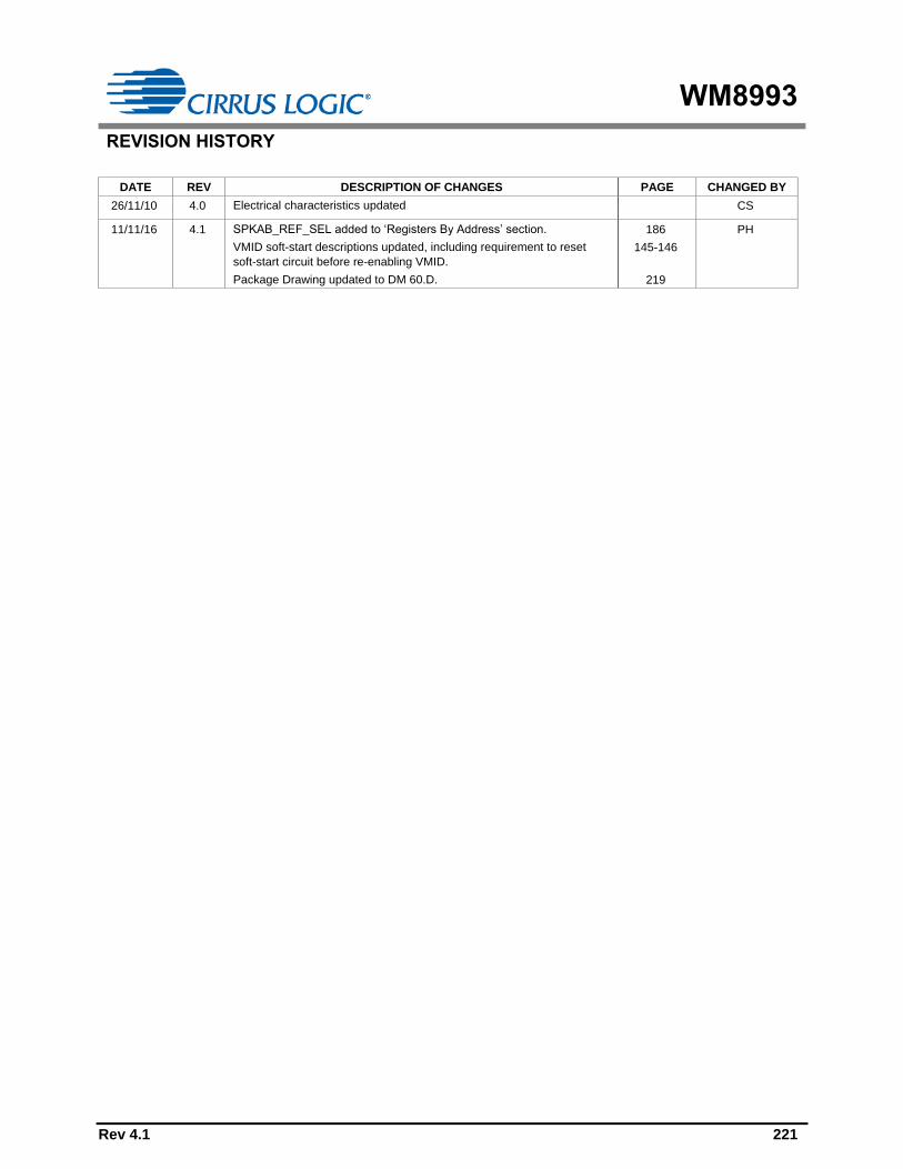
WM8993
Rev 4.1 221
REVISION HISTORY
DATE REV DESCRIPTION OF CHANGES PAGE CHANGED BY
26/11/10 4.0 Electrical characteristics updated CS
11/11/16 4.1 SPKAB_REF_SEL added to ‘Registers By Address’ section.
VMID soft-start descriptions updated, including requirement to reset
soft-start circuit before re-enabling VMID.
Package Drawing updated to DM 60.D.
186
145-146
219
PH