WM8950 Level Control DSP Core - Cirrus...
60
ADC with Microphone Input and Programmable Digital Filters http://www.cirrus.com Copyright Cirrus Logic, Inc., 2005–2016 (All Rights Reserved) Rev 4.5 AUG ‘16 WM8950 DESCRIPTION The WM8950 is a low power, high quality mono ADC designed for portable applications such as Digital Still Camera, Digital Voice Recorder or games console accessories. The device integrates support for a differential or single ended mic. External component requirements are reduced as no separate microphone amplifiers are required. Advanced Sigma Delta Converters are used along with digital decimation filters to give high quality audio at sample rates from 8 to 48ks/s. Additional digital filtering options are available, to cater for application filtering such as wind noise reduction, noise rejection, plus an advanced mixed signal ALC function with noise gate is provided. An on-chip PLL is provided to generate the required Master Clock from an external reference clock. The PLL clock can also be output if required elsewhere in the system. The WM8950 operates at supply voltages from 2.5 to 3.6V, although the digital supplies can operate at voltages down to 1.71V to save power. Different sections of the chip can also be powered down under software control by way of the selectable two or three wire control interface. WM8950 is supplied in a very small 4x4mm QFN package, offering high levels of functionality in minimum board area, with high thermal performance. FEATURES Mono ADC: Audio sample rates:8, 11.025, 16, 22.05, 24, 32, 44.1, 48kHz SNR 94dB, THD -83dB (‘A’-weighted @ 8 – 48ks/s) Multiple auxiliary analogue inputs Mic Preamps: Differential or single end Microphone Interface - Programmable preamp gain - Pseudo differential inputs with common mode rejection - Programmable ALC / Noise Gate in ADC path Low-noise bias supplied for electret microphones OTHER FEATURES 5 band EQ Programmable High-Pass Filter (wind noise reduction) Fully Programmable IIR Filter (notch filter) On-chip PLL Low power, low voltage - 2.5V to 3.6V (digital: 1.71V to 3.6V) - power consumption 10mA all-on 48ks/s mode 4x4x0.9mm 24 lead QFN package APPLICATIONS Digital Still Camera General Purpose low power audio ADC Games console accessories Voice recorders CONTROL INTERFACE CSB/GPIO SDIN SCLK MICBIAS WM8950 DGND AVDD AGND VMID 500k 500k I 2 S or PCM Interface ADC ADC Digital Filters PLL 50k 50k 4k 5k MCLK DBVDD AVDD2 AGND2 AUX 20k 20k analog inputs Rbias Mic NOISY GND Gains: -12dB to +35.25dB DCVDD MODE MICN MICP IP PGA IP BOOST/MIX FRAME ADCDAT TP BCLK Automatic Level Control 5 Band EQ Programmable High Pass Filter IIR Filter with Programmable Coefficients DSP Core
Transcript of WM8950 Level Control DSP Core - Cirrus...

ADC with Microphone Input and Programmable Digital Filters
http://www.cirrus.com
Copyright Cirrus Logic, Inc., 2005–2016
(All Rights Reserved)
Rev 4.5
AUG ‘16
WM8950
DESCRIPTION
The WM8950 is a low power, high quality mono ADC designed
for portable applications such as Digital Still Camera, Digital
Voice Recorder or games console accessories.
The device integrates support for a differential or single ended
mic. External component requirements are reduced as no
separate microphone amplifiers are required.
Advanced Sigma Delta Converters are used along with digital
decimation filters to give high quality audio at sample rates
from 8 to 48ks/s. Additional digital filtering options are
available, to cater for application filtering such as wind noise
reduction, noise rejection, plus an advanced mixed signal ALC
function with noise gate is provided.
An on-chip PLL is provided to generate the required Master
Clock from an external reference clock. The PLL clock can
also be output if required elsewhere in the system.
The WM8950 operates at supply voltages from 2.5 to 3.6V,
although the digital supplies can operate at voltages down to
1.71V to save power. Different sections of the chip can also be
powered down under software control by way of the selectable
two or three wire control interface.
WM8950 is supplied in a very small 4x4mm QFN package,
offering high levels of functionality in minimum board area, with
high thermal performance.
FEATURES
Mono ADC:
Audio sample rates:8, 11.025, 16, 22.05, 24, 32, 44.1, 48kHz
SNR 94dB, THD -83dB (‘A’-weighted @ 8 – 48ks/s)
Multiple auxiliary analogue inputs
Mic Preamps:
Differential or single end Microphone Interface
- Programmable preamp gain
- Pseudo differential inputs with common mode rejection
- Programmable ALC / Noise Gate in ADC path
Low-noise bias supplied for electret microphones
OTHER FEATURES
5 band EQ
Programmable High-Pass Filter (wind noise reduction)
Fully Programmable IIR Filter (notch filter)
On-chip PLL
Low power, low voltage
- 2.5V to 3.6V (digital: 1.71V to 3.6V)
- power consumption 10mA all-on 48ks/s mode
4x4x0.9mm 24 lead QFN package
APPLICATIONS
Digital Still Camera
General Purpose low power audio ADC
Games console accessories
Voice recorders
CONTROL
INTERFACE
CS
B/G
PIO
SD
IN
SC
LK
MICBIAS
WM8950
DGND
AV
DD
AG
ND
VM
ID
500k500k
I2S or
PCM
Interface
ADCADC
Digital
Filters
PLL50k 50k
4k 5k
MC
LK
DBVDD AVDD2AGND2
AUX
20k
20k
analog
inputs
Rbias
Mic
NOISY
GND
Gains:
-12dB to +35.25dB
DCVDD
MO
DE
MICN
MICPIP PGA
IP BOOST/MIX
FRAME
ADCDAT
TP
BCLK
Automatic
Level Control
5 Band
EQ
Programmable
High Pass
Filter
IIR Filter with
Programmable
Coefficients
DSP Core

WM8950
2 Rev 4.5
TABLE OF CONTENTS
DESCRIPTION ....................................................................................................... 1
FEATURES ............................................................................................................ 1
APPLICATIONS ..................................................................................................... 1
TABLE OF CONTENTS ......................................................................................... 2
PIN CONFIGURATION .......................................................................................... 3
ORDERING INFORMATION .................................................................................. 3
PIN DESCRIPTION ................................................................................................ 4
ABSOLUTE MAXIMUM RATINGS ........................................................................ 5
RECOMMENDED OPERATING CONDITIONS ..................................................... 5
ELECTRICAL CHARACTERISTICS ..................................................................... 6 TERMINOLOGY ............................................................................................................... 7
SIGNAL TIMING REQUIREMENTS ...................................................................... 8 SYSTEM CLOCK TIMING ................................................................................................ 8 AUDIO INTERFACE TIMING – MASTER MODE ............................................................ 8 AUDIO INTERFACE TIMING – SLAVE MODE ................................................................ 9 CONTROL INTERFACE TIMING – 3-WIRE MODE ....................................................... 10 CONTROL INTERFACE TIMING – 2-WIRE MODE ....................................................... 11
DEVICE DESCRIPTION ...................................................................................... 12 INTRODUCTION ............................................................................................................ 12 INPUT SIGNAL PATH .................................................................................................... 13 ANALOGUE TO DIGITAL CONVERTER (ADC) ............................................................ 18 INPUT AUTOMATIC LEVEL CONTROL (ALC) ............................................................. 22 DIGITAL AUDIO INTERFACES ..................................................................................... 36 AUDIO SAMPLE RATES ................................................................................................ 41 MASTER CLOCK AND PHASE LOCKED LOOP (PLL) ................................................. 42 GENERAL PURPOSE INPUT/OUTPUT ........................................................................ 44 CONTROL INTERFACE ................................................................................................. 44 RESETTING THE CHIP ................................................................................................. 45 POWER SUPPLIES ....................................................................................................... 46 ADC POWER UP/DOWN SEQUENCE .......................................................................... 46 POWER MANAGEMENT ............................................................................................... 47
REGISTER MAP .................................................................................................. 49
DIGITAL FILTER CHARACTERISTICS .............................................................. 50 TERMINOLOGY ............................................................................................................. 50 ADC FILTER RESPONSES ........................................................................................... 50 DE-EMPHASIS FILTER RESPONSES .......................................................................... 51 HIGH-PASS FILTER ...................................................................................................... 52 5-BAND EQUALISER ..................................................................................................... 53
APPLICATIONS INFORMATION ........................................................................ 57 RECOMMENDED EXTERNAL COMPONENTS ............................................................ 57
PACKAGE DIAGRAM ......................................................................................... 58
IMPORTANT NOTICE ......................................................................................... 59
REVISION HISTORY ........................................................................................... 60

WM8950
Rev 4.5 3
PIN CONFIGURATION
MC
LK
MODE
FR
AM
E
BC
LK
TP
AD
CD
AT
1
2
3
4
5
6
18
17
16
15
14
13
121110987
192021222324
WM8950
(Top View)D
NC
VM
ID
AV
DD
2
AU
X
MIC
N
MIC
P
AVDD
AGND
DGND
DCVDD
DBVDD
MICBIAS AGND2
DNC
SCLK
CS
B/G
PIO
SDIN
DNC
ORDERING INFORMATION
ORDER CODE TEMPERATURE
RANGE
PACKAGE MOISTURE SENSITIVITY
LEVEL
PACKAGE BODY
TEMPERATURE
WM8950CGEFL/V -40C to +85C
24-lead QFN (4x4x0.9mm)
(Pb-free)
MSL3 260oC
WM8950CGEFL/RV -40C to +85C
24-lead QFN (4x4x0.9mm)
(Pb-free, tape and reel)
MSL3 260oC
Note:
Reel Quantity = 3,500

WM8950
4 Rev 4.5
PIN DESCRIPTION
PIN NO NAME TYPE DESCRIPTION
1 MICBIAS Analogue Output Microphone bias
2 AVDD Supply Analogue supply (feeds ADC)
3 AGND Supply Analogue ground (feeds ADC)
4 DCVDD Supply Digital core supply
5 DBVDD Supply Digital buffer (input/output) supply
6 DGND Supply Digital ground
7 ADCDAT Digital Output ADC digital audio data output
8 TP Test Pin Connect to ground
9 FRAME Digital Input / Output ADC sample rate clock or frame synch
10 BCLK Digital Input / Output Digital audio bit clock
11 MCLK Digital Input Master clock input
12 CSB/GPIO Digital Input / Output 3-Wire MPU chip select or general purpose input/output pin.
13 SCLK Digital Input 3-Wire MPU clock Input / 2-Wire MPU Clock Input
14 SDIN Digital Input / Output 3-Wire MPU data Input / 2-Wire MPU Data Input
15 MODE Digital Input Control interface mode selection pin.
16 DNC Do not connect Leave this pin floating
17 DNC Do not connect Leave this pin floating
18 AGND2 Supply Analogue ground
19 DNC Do not connect Leave this pin floating
20 AVDD2 Supply Analogue supply
21 AUX Analogue Input Auxiliary analogue input
22 VMID Reference Decoupling for midrail reference voltage
23 MICN Analogue Input Microphone negative input
24 MICP Analogue Input Microphone positive input (common mode)
Note:
It is recommended that the QFN ground paddle should be connected to analogue ground on the application PCB.

WM8950
Rev 4.5 5
ABSOLUTE MAXIMUM RATINGS
Absolute Maximum Ratings are stress ratings only. Permanent damage to the device may be caused by continuously operating
at or beyond these limits. Device functional operating limits and guaranteed performance specifications are given under
Electrical Characteristics at the test conditions specified.
ESD Sensitive Device. This device is manufactured on a CMOS process. It is therefore generically susceptible to
damage from excessive static voltages. Proper ESD precautions must be taken during handling and storage of this
device.
Cirrus Logic tests its package types according to IPC/JEDEC J-STD-020B for Moisture Sensitivity to determine acceptable storage
conditions prior to surface mount assembly. These levels are:
MSL1 = unlimited floor life at <30C / 85% Relative Humidity. Not normally stored in moisture barrier bag.
MSL2 = out of bag storage for 1 year at <30C / 60% Relative Humidity. Supplied in moisture barrier bag.
MSL3 = out of bag storage for 168 hours at <30C / 60% Relative Humidity. Supplied in moisture barrier bag.
The Moisture Sensitivity Level for each package type is specified in Ordering Information.
CONDITION MIN MAX
DBVDD, DCVDD, AVDD, AVDD2 supply voltages -0.3V +4.2
Voltage range digital inputs DGND -0.3V DVDD +0.3V
Voltage range analogue inputs AGND -0.3V AVDD +0.3V
Operating temperature range, TA -40C +85C
Storage temperature prior to soldering 30C max / 85% RH max
Storage temperature after soldering -65C +150C
Notes:
1. Analogue and digital grounds must always be within 0.3V of each other.
2. All digital and analogue supplies are completely independent from each other.
RECOMMENDED OPERATING CONDITIONS
PARAMETER SYMBOL MIN TYP MAX UNIT
Digital supply range (Core) DCVDD 1.71 3.6 V
Digital supply range (Buffer) DBVDD 1.71 3.6 V
Analogue supplies range AVDD, AVDD2 2.5 3.6 V
Ground DGND, AGND, AGND2 0 V
Notes:
1. When using PLL, DCVDD must be 1.9V or higher.
2. AVDD must be DBVDD and DCVDD.
3. DBVDD must be DCVDD.
4. When using PLL, DCVDD must be 1.9V.

WM8950
6 Rev 4.5
ELECTRICAL CHARACTERISTICS
Test Conditions
DCVDD = 1.8V, AVDD = DBVDD = 3.3V, SPKVDD = 3.3V, TA = +25oC, 1kHz signal, fs = 48kHz,
24-bit audio data unless otherwise stated.
PARAMETER SYMBOL TEST CONDITIONS MIN TYP MAX UNIT
Microphone Inputs (MICN, MICP)
Full-scale Input Signal Level
(Note 1) – note this changes with
AVDD
VINFS PGABOOST = 0dB
INPPGAVOL = 0dB
1.0
0
Vrms
dBV
Mic PGA equivalent input noise At 35.25dB
gain
150 uV
Input resistance RMICIN Gain set to 35.25dB 1.6 k
Input resistance RMICIN Gain set to 0dB 47 k
Input resistance RMICIN Gain set to -12dB 75 k
Input resistance RMICIP (Constant for all gain
settings)
94 k
Input Capacitance CMICIN 10 pF
MIC Input Programmable Gain Amplifier (PGA)
Maximum Programmable Gain 35.25 dB
Minimum Programmable Gain -12 dB
Programmable Gain Step Size Guaranteed monotonic 0.75 dB
Mute Attenuation 108 dB
Selectable Input Gain Boost (0/+20dB)
Gain Boost 0 20 dB
Automatic Level Control (ALC)/Limiter
Target Record Level -28.5 -6 dB
Maximum Programmable Gain 35.25 dB
Minimum Programmable Gain -12 dB
Programmable Gain Step Size Guaranteed Monotonic 0.75 dB
Gain Hold Time (Note 2) tHOLD MCLK=12.288MHz
(Note 4)
0, 2.67, 5.33, 10.67, … , 43691
(time doubles with each step)
ms
Gain Ramp-Up (Decay) Time
(Note 3)
tDCY ALCMODE=0 (ALC),
MCLK=12.288MHz
(Note 4)
3.3, 6.6, 13.1, … , 3360
(time doubles with each step)
ms
ALCMODE=1 (limiter),
MCLK=12.288MHz
(Note 4)
0.73, 1.45, 2.91, … , 744
(time doubles with each step)
Gain Ramp-Down (Attack) Time
(Note 3)
tATK ALCMODE=0 (ALC),
MCLK=12.288MHz
(Note 4)
0.83, 1.66, 3.33, … , 852
(time doubles with each step)
ms
ALCMODE=1 (limiter),
MCLK=12.288MHz
(Note 4)
0.18, 0.36, 0.73, … , 186
(time doubles with each step)
Analogue to Digital Converter (ADC)
Signal to Noise Ratio (Note 5, 6) A-weighted,
0dB PGA gain
85 94 dB
Total Harmonic Distortion + Noise
(Note 6)
THD+N -1dBFS input
0dB PGA gain
-75 -83 dB
Auxiliary Analogue Input (AUX)
Full-scale Input Signal Level (0dB)
– note this changes with AVDD
VINFS 1.0
0
Vrms
dBV
Input Resistance RAUXIN AUXMODE=0 20 k
Input Capacitance CAUXIN 10 pF

WM8950
Rev 4.5 7
Test Conditions
DCVDD = 1.8V, AVDD = DBVDD = 3.3V, SPKVDD = 3.3V, TA = +25oC, 1kHz signal, fs = 48kHz,
24-bit audio data unless otherwise stated.
PARAMETER SYMBOL TEST CONDITIONS MIN TYP MAX UNIT
Microphone Bias
Bias Voltage (MBVSEL=0) VMICBIAS 0.9 x AVDD V
Bias Voltage (MBVSEL=1) VMICBIAS 0.75 x AVDD V
Bias Current Source IMICBIAS 3 mA
Output Noise Voltage Vn 1K to 20kHz 15 nV/Hz
Digital Input / Output
Input HIGH Level VIH 0.7 DVDD V
Input LOW Level VIL 0.3 DVDD V
Output HIGH Level VOH IOL=1mA 0.9 DVDD V
Output LOW Level VOL IOH-1mA 0.1 x DVDD V
TERMINOLOGY
1. MICN input only in single ended microphone configuration. Maximum input signal to MICP without distortion is -3dBV.
2. Hold Time is the length of time between a signal detected being too quiet and beginning to ramp up the gain. It does not
apply to ramping down the gain when the signal is too loud, which happens without a delay.
3. Ramp-up and Ramp-Down times are defined as the time it takes for the PGA to change its gain by 6dB.
4. All hold, ramp-up and ramp-down times scale proportionally with MCLK
5. Signal-to-noise ratio (dB) – SNR is a measure of the difference in level between the full scale output and the output with
no signal applied. (No Auto-zero or Automute function is employed in achieving these results).
6. THD+N (dB) – THD+N is a ratio, of the rms values, of (Noise + Distortion)/Signal.

WM8950
8 Rev 4.5
SIGNAL TIMING REQUIREMENTS
SYSTEM CLOCK TIMING
MCLK
tMCLKL
tMCLKH
tMCLKY
Figure 1 System Clock Timing Requirements
Test Conditions
DCVDD=1.8V, DBVDD=AVDD=SPKVDD=3.3V, DGND=AGND=SPKGND=0V, TA = +25oC, Slave Mode fs = 48kHz,
MCLK = 256fs, 24-bit data, unless otherwise stated.
PARAMETER SYMBOL CONDITIONS MIN TYP MAX UNIT
System Clock Timing Information
MCLK cycle time TMCLKY
MCLK as direct SYSCLK source
(CLKSEL=0)
81.38 ns
MCLK as input to PLL (see note)
(CLKSEL=1)
20 ns
MCLK duty cycle TMCLKDS 60:40 40:60
Note: PLL pre-scaling and PLL N and K values should be set appropriately so that SYSCLK is no greater than 12.288MHz.
AUDIO INTERFACE TIMING – MASTER MODE
BCLK
(Output)
ADCDAT
FRAME
(Output)
tDL
tDDA
Figure 2 Digital Audio Data Timing – Master Mode (see Control Interface)
Test Conditions
DCVDD=1.8V, DBVDD=AVDD=SPKVDD=3.3V, DGND=AGND=SPKGND=0V, TA = +25oC, Master Mode, fs=48kHz,
MCLK=256fs, 24-bit data, unless otherwise stated.
PARAMETER SYMBOL MIN TYP MAX UNIT
Audio Data Input Timing Information
FRAME propagation delay from BCLK falling edge tDL 10 ns
ADCDAT propagation delay from BCLK falling edge tDDA 10 ns

WM8950
Rev 4.5 9
AUDIO INTERFACE TIMING – SLAVE MODE
BCLK
FRAME
tBCH
tBCL
tBCY
ADCDAT
tLRSUt
LRHtDD
Figure 3 Digital Audio Data Timing – Slave Mode
Test Conditions
DCVDD=1.8V, DBVDD=AVDD=SPKVDD=3.3V, DGND=AGND=SPKGND=0V, TA=+25oC, Slave Mode, fs=48kHz, MCLK= 256fs,
24-bit data, unless otherwise stated.
PARAMETER SYMBOL MIN TYP MAX UNIT
Audio Data Input Timing Information
BCLK cycle time tBCY 50 ns
BCLK pulse width high tBCH 20 ns
BCLK pulse width low tBCL 20 ns
FRAME set-up time to BCLK rising edge tLRSU 10 ns
FRAME hold time from BCLK rising edge tLRH 10 ns
ADCDAT propagation delay from BCLK falling edge tDD 20 ns
Note: BCLK period should always be greater than or equal to MCLK period.

WM8950
10 Rev 4.5
CONTROL INTERFACE TIMING – 3-WIRE MODE
CSB/GPIO
SCLK
SDIN
tCSL
tDHO
tDSU
tCSH
tSCY
tSCH
tSCL
tSCS
LSB
tCSS
Figure 4 Control Interface Timing – 3-Wire Serial Control Mode
Test Conditions
DCVDD = 1.8V, DBVDD = AVDD = SPKVDD = 3.3V, DGND = AGND = SPKGND = 0V, TA = +25oC, Slave Mode, fs = 48kHz,
MCLK = 256fs, 24-bit data, unless otherwise stated.
PARAMETER SYMBOL MIN TYP MAX UNIT
Program Register Input Information
SCLK rising edge to CSB rising edge tSCS 80 ns
SCLK pulse cycle time tSCY 200 ns
SCLK pulse width low tSCL 80 ns
SCLK pulse width high tSCH 80 ns
SDIN to SCLK set-up time tDSU 40 ns
SCLK to SDIN hold time tDHO 40 ns
CSB pulse width low tCSL 40 ns
CSB pulse width high tCSH 40 ns
CSB rising to SCLK rising tCSS 40 ns
Pulse width of spikes that will be suppressed tps 0 5 ns

WM8950
Rev 4.5 11
CONTROL INTERFACE TIMING – 2-WIRE MODE
SDIN
SCLK
t3
t1
t6 t
2
t7
t5
t4
t3
t8
t9
Figure 5 Control Interface Timing – 2-Wire Serial Control Mode
Test Conditions
DCVDD=1.8V, DBVDD=AVDD=SPKVDD=3.3V, DGND=AGND=SPKGND=0V, TA = +25oC, Slave Mode, fs = 48kHz,
MCLK = 256fs, 24-bit data, unless otherwise stated.
PARAMETER SYMBOL MIN TYP MAX UNIT
Program Register Input Information
SCLK Frequency 0 526 kHz
SCLK Low Pulse-Width t1 1.3 us
SCLK High Pulse-Width t2 600 ns
Hold Time (Start Condition) t3 600 ns
Setup Time (Start Condition) t4 600 ns
Data Setup Time t5 100 ns
SDIN, SCLK Rise Time t6 300 ns
SDIN, SCLK Fall Time t7 300 ns
Setup Time (Stop Condition) t8 600 ns
Data Hold Time t9 900 ns
Pulse width of spikes that will be suppressed tps 0 5 ns

WM8950
12 Rev 4.5
DEVICE DESCRIPTION
INTRODUCTION
The WM8950 is a low power audio ADC, with flexible line and microphone input. Applications for this
device include games console accessories, digital still cameras, voice recorders and other general
purpose audio applications.
The chip offers great flexibility in use, and so can support many different modes of operation as
follows:
MICROPHONE INPUTS
Microphone inputs are provided, allowing for either a differential microphone input or a single ended
microphone to be connected. These inputs have a user programmable gain range of -12dB to
+35.25dB using internal resistors. After the input PGA stage comes a boost stage which can add a
further 20dB of gain. A microphone bias is output from the chip which can be used to bias the
microphones. The signal routing can be configured to allow manual adjustment of mic levels, or to
allow the ALC loop to control the level of mic signal that is transmitted.
Total gain through the microphone paths of up to +55.25dB can be selected.
PGA AND ALC OPERATION
A programmable gain amplifier is provided in the input path to the ADC. This may be used manually
or in conjunction with a mixed analogue/digital automatic level control (ALC) which keeps the
recording volume constant.
AUX INPUT
The device includes a mono input, AUX, that can be used as an input for warning tones (beep) etc.
This path can also be summed into the input in a flexible fashion, either to the input PGA as a second
microphone input or as a line input. The configuration of this circuit, with integrated on-chip resistors
allows several analogue signals to be summed into the single AUX input if required.
ADC
The mono ADC uses a multi-bit high-order oversampling architecture to deliver optimum performance
with low power consumption. Various sample rates are supported, from the 8ks/s rate typically used
in voice dictation, up to the 48ks/s rate used in high quality audio applications.
DIGITAL FILTERING
Advanced Sigma Delta Converters are used along with digital decimation and interpolation filters to
give high quality audio at sample rates from 8ks/s to 48ks/s.
Application specific digital filters are also available which help to reduce the effect of specific noise
sources such as ‘wind noise’. The filters include a programmable ADC high-pass filter, an IIR filter
with fully programmable coefficients, and a 5-band equaliser that can be applied to the record path in
order to improve the overall audio sound from the device.
AUDIO INTERFACES
The WM8950 has a standard audio interface, to support the transmission of audio data from the chip.
This interface is a 4 wire standard audio interface which supports a number of audio data formats
including I2S, DSP Mode, MSB-First, left justified and MSB-First, right justified, and can operate in
master or slave modes.
CONTROL INTERFACES
To allow full software control over all its features, the WM8950 offers a choice of 2 or 3 wire MPU
control interface. It is fully compatible and an ideal partner for a wide range of industry standard
microprocessors, controllers and DSPs. The selection between 2-wire mode and 3-wire mode is
determined by the state of the MODE pin. If MODE is high then 3-wire control mode is selected, if
MODE is low then 2-wire control mode is selected.
In 2 wire mode, only slave operation is supported, and the address of the device is fixed as 0011010.
CLOCKING SCHEMES
WM8950 offers the normal audio clocking scheme operation, where 256fs MCLK is provided to the
ADC.

WM8950
Rev 4.5 13
However, a PLL is also included which may be used to generate the internal master clock frequency
in the event that this is not available from the system controller. The PLL uses an input reference
(typically, the 12MHz USB clock) to generate high quality audio clocks. If the PLL is not required for
generation of these clocks, it can be reconfigured to generate alternative clocks which may then be
output on the CSB/GPIO pin and used elsewhere in the system.
POWER CONTROL
The design of the WM8950 has given much attention to power consumption without compromising
performance. It operates at low supply voltages, and includes the facility to power off any unused
parts of the circuitry under software control, includes standby and power off modes.
INPUT SIGNAL PATH
The WM8950 has 3 flexible analogue inputs: two microphone inputs, and an auxiliary input. These
inputs can be used in a variety of ways. The input signal path before the ADC has a flexible PGA
block which then feeds into a gain boost/mixer stage.
MICROPHONE INPUTS
The WM8950 can accommodate a variety of microphone configurations including single ended and
differential inputs. The inputs through the MICN, MICP and optionally AUX pins are amplified through
the input PGA as shown in Figure 6 .
A pseudo differential input is the preferential configuration where the positive terminal of the input
PGA is connected to the MICP input pin by setting MICP2INPPGA=1. The microphone ground
should then be connected to MICN (when MICN2INPPGA=1) or optionally to AUX (when
AUX2INPPGA=1) input pins.
Alternatively a single ended microphone can be connected to the MICN input with MICN2INPPGA set
to 1. The non-inverting terminal of the input PGA should be connected internally to VMID by setting
MICP2INPPGA to 0.
Output from
AUX amp
MICP
MICN
VMID
AUX2INPPGA
R44[2]
MICN2INPPGA
R44[1]
MICP2INPPGA
R44[0] To input
BOOST/mix
stage
INPPGAVOL
R45[5:0]
Gain=-12 to +35.25dB
Figure 6 Microphone Input PGA Circuit (switch positions shown are for differential mic
input)

WM8950
14 Rev 4.5
REGISTER
ADDRESS
BIT LABEL DEFAULT DESCRIPTION
R44
Input Control
0 MICP2INPPGA 1 Connect input PGA amplifier positive
terminal to MICP or VMID.
0 = input PGA amplifier positive terminal
connected to VMID
1 = input PGA amplifier positive terminal
connected to MICP through variable resistor
string
1 MICN2INPPGA 1 Connect MICN to input PGA negative
terminal.
0=MICN not connected to input PGA
1=MICN connected to input PGA amplifier
negative terminal.
2 AUX2INPPGA 0 Select AUX amplifier output as input PGA
signal source.
0=AUX not connected to input PGA
1=AUX connected to input PGA amplifier
negative terminal.
The input PGA is enabled by the IPPGAEN register bit.
REGISTER
ADDRESS
BIT LABEL DEFAULT DESCRIPTION
R2
Power
Management 2
2 INPPGAEN 0 Input microphone PGA enable
0 = disabled
1 = enabled
INPUT PGA VOLUME CONTROL
The input microphone PGA has a gain range from -12dB to +35.25dB in 0.75dB steps. The gain
from the MICN input to the PGA output and from the AUX amplifier to the PGA output are always
common and controlled by the register bits INPPGAVOL[5:0]. These register bits also affect the
MICP pin when MICP2INPPGA=1.
When the Automatic Level Control (ALC) is enabled the input PGA gain is then controlled
automatically and the INPPGAVOL bits should not be used.
REGISTER
ADDRESS
BIT LABEL DEFAULT DESCRIPTION
R45
Input PGA
volume
control
5:0 INPPGAVOL 010000 Input PGA volume
000000 = -12dB
000001 = -11.25dB
.
010000 = 0dB
.
111111 = 35.25dB
6 INPPGAMUTE 0 Mute control for input PGA:
0=Input PGA not muted, normal operation
1=Input PGA muted (and disconnected from
the following input BOOST stage).
7 INPPGAZC 0 Input PGA zero cross enable:
0=Update gain when gain register changes
1=Update gain on 1st zero cross after gain
register write.

WM8950
Rev 4.5 15
REGISTER
ADDRESS
BIT LABEL DEFAULT DESCRIPTION
R32
ALC control 1
8 ALCSEL 0 ALC function select:
0=ALC off (PGA gain set by INPPGAVOL
register bits)
1=ALC on (ALC controls PGA gain)
Table 1 Input PGA Volume Control
AUXILIARY INPUT
An auxiliary input circuit (Figure 7) is provided which consists of an amplifier which can be configured
either as an inverting buffer for a single input signal or as a mixer/summer for multiple inputs with the
use of external resistors. The circuit is enabled by the register bit AUXEN.
-
+
VMID
AUX
20k
20k
AUXSW closed
when summing
multiple inputs
To INP PGA,
INP BOOST or
output MIXERS
AUXMODE
R44[3]
AUXSW
AUXOP
Figure 7 Auxiliary Input Circuit
The AUXMODE register bit controls the auxiliary input mode of operation:
In buffer mode (AUXMODE=0) the switch labelled AUXSW in Figure 7 is open and the signal at the
AUX pin will be buffered and inverted through the aux circuit using only the internal components.
In mixer mode (AUXMODE=1) the on-chip input resistor is bypassed, this allows the user to sum in
multiple inputs with the use of external resistors. When used in this mode there will be gain
variations through this path from part to part due to the variation of the internal 20kΩ resistors relative
to the higher tolerance external resistors.
REGISTER
ADDRESS
BIT LABEL DEFAULT DESCRIPTION
R1
Power
management 1
6 AUXEN 0 Auxiliary input buffer enable
0 = OFF
1 = ON
R44
Input control
3 AUXMODE 0 0 = inverting buffer
1 = mixer (on-chip input resistor bypassed)
Table 2 Auxiliary Input Buffer Control

WM8950
16 Rev 4.5
INPUT BOOST
The input BOOST circuit has 3 selectable inputs: the input microphone PGA output, the AUX
amplifier output and the MICP input pin (when not using a differential microphone configuration).
These three inputs can be mixed together and have individual gain boost/adjust as shown in Figure
8.
To ADC input
and output
mixers
AUX2BOOSTVOL=000
MICP2BOOSTVOL=000
Output from
AUX amp
Output from
input PGA
MICP
AUX2BOOSTVOL
R47[2:0]
MICP2BOOSTVOL
R47[6:4]
INPPGAMUTE
R45[6]
PGABOOST
R47[8]
-12dB to + 6dB
-12dB to + 6dB
0dB or +20dB
Figure 8 Input Boost Stage
The input PGA path can have a +20dB boost (PGABOOST=1) a 0dB pass through (PGABOOST=0)
or be completely isolated from the input boost circuit (INPPGAMUTE=1).
REGISTER
ADDRESS
BIT LABEL DEFAULT DESCRIPTION
R45
Input PGA gain
control
6 INPPGAMUTE 0 Mute control for input PGA:
0=Input PGA not muted, normal operation
1=Input PGA muted (and disconnected from
the following input BOOST stage).
R47
Input BOOST
control
8 PGABOOST 1 0 = PGA output has +0dB gain through input
BOOST stage.
1 = PGA output has +20dB gain through
input BOOST stage.
Table 3 Input BOOST Stage Control
The Auxiliary amplifier path to the BOOST stage is controlled by the AUX2BOOSTVOL[2:0] register
bits. When AUX2BOOSTVOL=000 this path is completely disconnected from the BOOST stage.
Settings 001 through to 111 control the gain in 3dB steps from -12dB to +6dB.
The MICP path to the BOOST stage is controlled by the MICP2BOOSTVOL[2:0] register bits. When
MICP2BOOSTVOL=000 this input pin is completely disconnected from the BOOST stage. Settings
001 through to 111 control the gain in 3dB steps from -12dB to +6dB.

WM8950
Rev 4.5 17
REGISTER
ADDRESS
BIT LABEL DEFAULT DESCRIPTION
R47
Input BOOST
control
2:0 AUX2BOOSTVOL 000 Controls the auxiliary amplifier to the input
boost stage:
000=Path disabled (disconnected)
001=-12dB gain through boost stage
010=-9dB gain through boost stage
…
111=+6dB gain through boost stage
6:4 MICP2BOOSTVOL 000 Controls the MICP pin to the input boost
stage (NB, when using this path set
MICPZIUNPPGA=0):
000=Path disabled (disconnected)
001=-12dB gain through boost stage
010=-9dB gain through boost stage
…
111=+6dB gain through boost stage
Table 4 Input BOOST Stage Control
The BOOST stage is enabled under control of the BOOSTEN register bit.
REGISTER
ADDRESS
BIT LABEL DEFAULT DESCRIPTION
R2
Power
management 2
4 BOOSTEN 0 Input BOOST enable
0 = Boost stage OFF
1 = Boost stage ON
Table 5 Input BOOST Enable Control
MICROPHONE BIASING CIRCUIT
The MICBIAS output provides a low noise reference voltage suitable for biasing electret type
microphones and the associated external resistor biasing network. Refer to the Applications
Information section for recommended external components. The MICBIAS voltage can be altered via
the MBVSEL register bit. If MBVSEL = 0, the MICBIAS voltage is 0.9 x AVDD. If MBVSEL = 1, the
MICBIAS voltage is 0.75 x AVDD. The output can be enabled or disabled using MICBEN.
REGISTER
ADDRESS
BIT LABEL DEFAULT DESCRIPTION
R1
Power
management 1
4 MICBEN 0 Microphone Bias Enable
0 = OFF (high impedance output)
1 = ON
Table 6 Microphone Bias Enable
REGISTER
ADDRESS
BIT LABEL DEFAULT DESCRIPTION
R44
Input Control
8 MBVSEL 0 Microphone Bias Voltage Control
0 = 0.9 x AVDD
1 = 0.75 x AVDD
Table 7 Microphone Bias Voltage Control
The internal MICBIAS circuitry is shown in Figure 9. Note that the maximum source current capability
for MICBIAS is 3mA. The external biasing resistors therefore must be large enough to limit the
MICBIAS current to 3mA.

WM8950
18 Rev 4.5
AGND
MBVSEL=0
MICBIAS
= 1.8 x VMID
= 0.9 x AVDD
VMID
internal
resistor
internal
resistor
MB
MBVSEL=1
MICBIAS
= 1.5 x VMID
= 0.75 x AVDD
Figure 9 Microphone Bias Schematic
ANALOGUE TO DIGITAL CONVERTER (ADC)
The WM8950 uses a multi-bit, oversampled sigma-delta ADC channel. The use of multi-bit feedback
and high oversampling rates reduces the effects of jitter and high frequency noise. The ADC Full
Scale input level is proportional to AVDD. With a 3.3V supply voltage, the full scale level is 1.0Vrms.
Any voltage greater than -1dBfs may overload the ADC and cause distortion.
ADC DIGITAL FILTERS
The ADC filters perform true 24 bit signal processing to convert the raw multi-bit oversampled data
from the ADC to the correct sampling frequency to be output on the digital audio interface. The digital
filter path is illustrated in Figure 10 .
ADCDIGITAL
DECIMATOR
DIGITAL
FILTERSGAIN
5-BAND
EQUALISER
HIGH PASS
FILTER
IIR
FILTER
DIGITAL
AUDIO
INTERFACE
ADC DIGITAL FILTERS
Figure 10 ADC Digital Filter Path
The ADC is enabled by the ADCEN register bit.
REGISTER
ADDRESS
BIT LABEL DEFAULT DESCRIPTION
R2
Power
management 2
0 ADCEN 0 0 = ADC disabled
1 = ADC enabled
Table 8 ADC Enable

WM8950
Rev 4.5 19
The polarity of the output signal can also be changed under software control using the ADCPOL
register bit. The oversampling rate of the ADC can be adjusted using the ADCOSR register bit.
With ADCOSR=0 the oversample rate is 64x which gives lowest power operation and when
ADCOSR=1 the oversample rate is 128x which gives best performance.
REGISTER
ADDRESS
BIT LABEL DEFAULT DESCRIPTION
R14
ADC Control
3 ADCOSR 0 ADC oversample rate select:
0=64x (lower power)
1=128x (best performance)
0 ADCPOL 0 0=normal
1=inverted
Table 9 ADC Oversample Rate Select
SELECTABLE HIGH-PASS FILTER
A selectable high-pass filter is provided. To disable this filter set HPFEN=0. The filter has two
modes controlled by HPFAPP. In Audio Mode (HPFAPP=0) the filter is first order, with a cut-off
frequency of 3.7Hz. In Application Mode (HPFAPP=1) the filter is second order, with a cut-off
frequency selectable via the HPFCUT register. The cut-off frequencies when HPFAPP=1 are shown
in Table 11.
REGISTER
ADDRESS
BIT LABEL DEFAULT DESCRIPTION
R14
ADC Control
8 HPFEN 1 High-Pass Filter Enable
0=disabled
1=enabled
7 HPFAPP 0 Select audio mode or application mode
0=Audio mode (1st order, fc = ~3.7Hz)
1=Application mode (2nd order, fc =
HPFCUT)
6:4 HPFCUT 000 Application mode cut-off frequency
See Table 11 for details.
Table 10 ADC Filter Select
HPFCUT
[2:0]
SAMPLE FREQUENCY (kHz)
8 11.025 12 16 22.05 24 32 44.1 48
SR=101/100 SR=011/010 SR=001/000
000 82 113 122 82 113 122 82 113 122
001 102 141 153 102 141 153 102 141 153
010 131 180 196 131 180 196 131 180 196
011 163 225 245 163 225 245 163 225 245
100 204 281 306 204 281 306 204 281 306
101 261 360 392 261 360 392 261 360 392
110 327 450 490 327 450 490 327 450 490
111 408 563 612 408 563 612 408 563 612
Table 11 High-Pass Filter Cut-off Frequencies (HPFAPP=1) Values in Hz
Note that the High-Pass filter values (when HPFAPP=1) work on the basis that the SR register bits
are set correctly for the actual sample rate as shown in Table 11.

WM8950
20 Rev 4.5
PROGRAMMABLE IIR FILTER
An IIR filter with fully programmable coefficients is provided, typically used as a notch filter for
removing narrow band noise at a given frequency. This notch filter has a variable centre frequency
and bandwidth, programmable via two coefficients, a0 and a1. These coefficients should be
converted to 2’s complement numbers to determine the register values. a0 and a1 are represented
by the register bits NFA0[13:0] and NFA1[13:0]. Because these coefficient values require four
register writes to setup there is an NFU (Notch Filter Update) flag which should be set only when all
four registers are setup.
REGISTER
ADDRESS
BIT LABEL DEFAULT DESCRIPTION
R27
Notch Filter 1
6:0 NFA0[13:7] 0 Notch filter a0 coefficient, bits [13:7]
7 NFEN 0 Notch filter enable:
0=Disabled
1=Enabled
8 NFU 0 Notch filter update. The notch filter values
used internally only update when one of
the NFU bits is set high.
R28
Notch Filter 2
6:0 NFA0[6:0] 0 Notch filter a0 coefficient, bits [6:0]
8 NFU] 0 Notch filter update. The notch filter values
used internally only update when one of
the NFU bits is set high.
R29
Notch Filter 3
6:0 NFA1[13:7] 0 Notch filter a1 coefficient, bits [13:7]
8 NFU 0 Notch filter update. The notch filter values
used internally only update when one of
the NFU bits is set high.
R30
Notch Filter 4
6:0 NFA1[6:0] 0 Notch filter a1 coefficient, bits [6:0]
8 NFU 0 Notch filter update. The notch filter values
used internally only update when one of
the NFU bits is set high.
Table 12 Notch Filter Function
The coefficients are calculated as follows:
)2/tan(1
)2/tan(10
b
b
w
wa
)cos()1( 001 waa
Where:
sc ffw /20
sbb ffw /2
fc = centre frequency in Hz, fb = -3dB bandwidth in Hz, fs = sample frequency in Hz
The coefficients are calculated as follows:
NFA0 = -a0 x 213
NFA1 = -a1 x 212
These values are then converted to 2’s complement notation to determine the register values.

WM8950
Rev 4.5 21
NOTCH FILTER WORKED EXAMPLE
The following example illustrates how to calculate the a0 and a1 coefficients for a desired centre
frequency and -3dB bandwidth.
fc = 1000 Hz
fb = 100 Hz
fs = 48000 Hz
sc0 f/f2w = 2 x (1000 / 48000) = 0.1308996939 rads
sbb f/f2w = 2 x (100 / 48000) = 0.01308996939 rads
)2/wtan(1
)2/wtan(1a
b
b0
= )2/90130899693.0tan(1
)2/90130899693.0tan(1
= 0.9869949627
)wcos()a1(a 001 =
)1308996939.0cos()9869949627.01( = -1.969995945
NFn_A0 = -a0 x 213 = -8085 (rounded to nearest whole number)
NFn_A1 = -a1 x 212 = 8069 (rounded to nearest whole number)
These values are then converted to 2’s complement:
NFA0 = 14’h206B = 14’b10000001101011
NFA1 = 14’h1F85 = 14’b01111110000101
DIGITAL ADC VOLUME CONTROL
The output of the ADCs can be digitally attenuated over a range from –127dB to 0dB in 0.5dB steps.
The gain for a given eight-bit code X is given by:
Gain = 0.5 x (x–255) dB for 1 x 255, MUTE for x = 0
REGISTER
ADDRESS
BIT LABEL DEFAULT DESCRIPTION
R15
ADC Digital
Volume
7:0 ADCVOL
[7:0]
11111111
( 0dB )
ADC Digital Volume Control
0000 0000 = Digital Mute
0000 0001 = -127dB
0000 0010 = -126.5dB
... 0.5dB steps up to
1111 1111 = 0dB
Table 13 ADC Volume

WM8950
22 Rev 4.5
INPUT AUTOMATIC LEVEL CONTROL (ALC)
The WM8950 has an automatic PGA gain control circuit, which can function as an input peak limiter
or as an automatic level control (ALC).
The Automatic Level Control (ALC) provides continuous adjustment of the input PGA in response to
the amplitude of the input signal. A digital peak detector monitors the input signal amplitude and
compares it to a register defined threshold level (ALCLVL).
If the signal is below the threshold, the ALC will increase the gain of the PGA at a rate set by
ALCDCY. If the signal is above the threshold, the ALC will reduce the gain of the PGA at a rate set
by ALCATK.
The ALC has two modes selected by the ALCMODE register: normal mode and peak limiter mode.
The ALC/limiter function is enabled by setting the register bit R32[8] ALCSEL.
REGISTER
ADDRESS
BIT LABEL DEFAULT DESCRIPTION
R32 (20h)
ALC Control 1
2:0 ALCMIN
[2:0]
000 (-12dB) Set minimum gain of PGA
000 = -12dB
001 = -6dB
010 = 0dB
011 = +6dB
100 = +12dB
101 = +18dB
110 = +24dB
111 = +30dB
5:3 ALCMAX
[2:0]
111
(+35.25dB)
Set Maximum Gain of PGA
111 = +35.25dB
110 = +29.25dB
101 = +23.25dB
100 = +17.25dB
011 = +11.25dB
010 = +5.25dB
001 = -0.75dB
000 = -6.75dB
8 ALCSEL 0 ALC function select
0 = ALC disabled
1 = ALC enabled
R33 (21h)
ALC Control 2
3:0 ALCLVL
[3:0]
1011
(-12dB)
ALC target – sets signal level at ADC input
1111 = -6dBFS
1110 = -7.5dBFS
1101 = -9dBFS
1100 = -10.5dBFS
1011 = -12dBFS
1010 = -13.5dBFS
1001 = -15dBFS
1000 = -16.5dBFS
0111 = -18dBFS
0110 = -19.5dBFS
0101 = -21dBFS
0100 = -22.5dBFS
0011 = -24dBFS
0010 = -25.5dBFS
0001 = -27dBFS
0000 = -28.5dBFS

WM8950
Rev 4.5 23
REGISTER
ADDRESS
BIT LABEL DEFAULT DESCRIPTION
8 ALCZC 0 (zero
cross off)
ALC uses zero cross detection circuit.
0 = Disabled (recommended)
1 = Enabled
7:4 ALCHLD
[3:0]
0000
(0ms)
ALC hold time before gain is increased.
0000 = 0ms
0001 = 2.67ms
0010 = 5.33ms
0011 = 10.66ms
0100 = 21.32ms
0101 = 42.64ms
0110 = 85.28ms
0111 = 0.17s
1000 = 0.34s
1001 = 0.68s
1010 or higher = 1.36s
R34 (22h)
ALC Control 3
8 ALCMODE 0 Determines the ALC mode of operation:
0 = ALC mode (Normal Operation)
1 = Limiter mode.
7:4 ALCDCY
[3:0]
0011
(26ms/6dB)
Decay (gain ramp-up) time
(ALCMODE ==0)
Per step Per 6dB 90% of
range
0000 410us 3.38ms 23.6ms
0001 820us 6.56ms 47.2ms
0010 1.64ms 13.1ms 94.5ms
… (time doubles with every step)
1010
or
higher
420ms 3.36s 24.2s
0011
(5.8ms/6dB)
Decay (gain ramp-up) time
(ALCMODE ==1)
Per step Per 6dB 90% of
range
0000 90.8us 726us 5.23ms
0001 182us 1.45ms 10.5ms
0010 363us 2.91ms 20.9ms
… (time doubles with every step)
1010 93ms 744ms 5.36s
3:0 ALCATK
[3:0]
0010
(3.3ms/6dB)
ALC attack (gain ramp-down) time
(ALCMODE == 0)
Per step Per 6dB 90% of
range
0000 104us 832us 6ms
0001 208us 1.66ms 12ms
0010 416us 3.33ms 24ms
… (time doubles with every step)
1010
or
higher
106ms 852ms 6.13s

WM8950
24 Rev 4.5
REGISTER
ADDRESS
BIT LABEL DEFAULT DESCRIPTION
0010
(726us/6dB)
ALC attack (gain ramp-down) time
(ALCMODE == 1)
Per step Per 6dB 90% of
range
0000 22.7us 182.4us 1.31ms
0001 45.4us 363us 2.62ms
0010 90.8us 726us 5.23ms
… (time doubles with every step)
1010 or
higher
23.2ms 186ms 1.34s
Table 14 ALC Control Registers
When the ALC is disabled, the input PGA remains at the last controlled value of the ALC. An input
gain update must be made by writing to the INPPGAVOLL/R register bits.
NORMAL MODE
In normal mode, the ALC will attempt to maintain a constant signal level by increasing or decreasing
the gain of the PGA. The following diagram shows an example of this.
Input
Signal
ALCSEL
PGA
Gain
ALCLVL
tATK t
DCY
Output
of PGA
Vstep
Figure 11 ALC Normal Mode Operation

WM8950
Rev 4.5 25
LIMITER MODE
In limiter mode, the ALC will reduce peaks that go above the threshold level, but will not increase the
PGA gain beyond the starting level. The starting level is the PGA gain setting when the ALC is
enabled in limiter mode. If the ALC is started in limiter mode, this is the gain setting of the PGA at
start-up. If the ALC is switched into limiter mode after running in ALC mode, the starting gain will be
the gain at switchover. The diagram below shows an example of limiter mode.
Input
Signal
ALCSEL
PGA
Gain
ALCLVL
tATKLIM
tDCYLIM
Output
of PGA
Vstep
Figure 12 ALC Limiter Mode Operation
ATTACK AND DECAY TIMES
The attack and decay times set the update times for the PGA gain. The attack time is the time
constant used when the gain is reducing. The decay time is the time constant used when the gain is
increasing. In limiter mode, the time constants are faster than in ALC mode. The time constants are
shown below in terms of a single gain step, a change of 6dB and a change of 90% of the PGAs gain
range.
Note that, these times will vary slightly depending on the sample rate used (specified by the SR
register).

WM8950
26 Rev 4.5
NORMAL MODE
ALCMODE = 0 (Normal Mode)
ALCATK tATK tATK6dB tATK90%
0000 104µs 832µs 6ms
0001 208µs 1.66ms 12ms
0010 416µs 3.33ms 24ms
0011 832µs 6.66ms 48ms
0100 1.66ms 13.3ms 96ms
0101 3.33ms 26.6ms 192ms
0110 6.66ms 53.2ms 384ms
0111 13.3ms 106ms 767ms
1000 26.6ms 213.2ms 1.53s
1001 53.2ms 426ms 3.07s
1010 106ms 852ms 6.13s
Attack Time (s)
ALCMODE = 0 (Normal Mode)
ALCDCY tDCY tDCY6dB tDCY90%
0000 410µs 3.28ms 23.6ms
0001 820µs 6.56ms 47.2ms
0010 1.64ms 13.1ms 94.5ms
0011 3.28ms 26.2ms 189ms
0100 6.56ms 52.5ms 378ms
0101 13.1ms 105ms 756ms
0110 26.2ms 210ms 1.51s
0111 52.5ms 420ms 3.02s
1000 105ms 840ms 6.05s
1001 210ms 1.68s 12.1s
1010 420ms 3.36s 24.2s
Decay Time (s)
Table 15 ALC Normal Mode (Attack and Decay times)
LIMITER MODE
ALCMODE = 1 (Limiter Mode)
ALCATK tATKLIM tATKLIM6dB tATKLIM90%
0000 22.7µs 182µs 1.31ms
0001 45.4µS 363µs 2.62ms
0010 90.8µS 726µs 5.23ms
0011 182µS 1.45ms 10.5ms
0100 363µS 2.91ms 20.9ms
0101 726µS 5.81ms 41.8ms
0110 1.45ms 11.6ms 83.7ms
0111 2.9ms 23.2ms 167ms
1000 5.81ms 46.5ms 335ms
1001 11.6ms 93ms 669ms
1010 23.2ms 186ms 1.34s
Attack Time (s)

WM8950
Rev 4.5 27
ALCMODE = 1 (Limiter Mode)
ALCDCY tDCYLIM tDCYLIM6dB tDCYLIM90%
0000 90.8µs 726µs 5.23ms
0001 182µS 1.45ms 10.5ms
0010 363µS 2.91ms 20.9ms
0011 726µS 5.81ms 41.8ms
0100 1.45ms 11.6ms 83.7ms
0101 2.91ms 23.2ms 167ms
0110 5.81ms 46.5ms 335ms
0111 11.6ms 93ms 669ms
1000 23.2ms 186ms 1.34s
1001 46.5ms 372ms 2.68s
1010 93ms 744ms 5.36s
Attack Time (s)
Table 16 ALC Limiter Mode (Attack and Decay times)
MINIMUM AND MAXIMUM GAIN
The ALCMIN and ALCMAX register bits set the minimum/maximum gain value that the PGA can be
set to whilst under the control of the ALC. This has no effect on the PGA when ALC is not enabled.
REGISTER
ADDRESS
BIT LABEL DEFAULT DESCRIPTION
R32
ALC Control 1
5:3 ALCMAX 111 Set Maximum Gain of PGA
2:0 ALCMIN 000 Set minimum gain of PGA
Table 17 ALC Max/Min Gain
In normal mode, ALCMAX sets the maximum boost which can be applied to the signal. In limiter
mode, ALCMAX will normally have no effect (assuming the starting gain value is less than the
maximum gain specified by ALCMAX) because the maximum gain is set at the starting gain level.
ALCMIN sets the minimum gain value which can be applied to the signal.
PGA Gain = 000000 (-12dB)
PGA Gain = 111111 (+35.25dB)
ALCMAX
ALCMIN
ALC operating range
Whole PGA gain range
Figure 13 ALC Min/Max Gain

WM8950
28 Rev 4.5
ALCMAX Maximum Gain (dB)
111 35.25
110 29.25
101 23.25
100 17.25
011 11.25
010 5.25
001 -0.75
000 -6.75
Table 18 ALC Max Gain Values
ALCMIN Minimum Gain (dB)
000 -12
001 -6
010 0
011 6
100 12
101 18
110 24
111 30
Table 19 ALC Min Gain Values
Note that if the ALC gain setting strays outside the ALC operating range, either by starting the ALC
outside of the range or changing the ALCMAX or ALCMIN settings during operation, the ALC will
immediately adjust the gain to return to the ALC operating range. It is recommended that the ALC
starting gain is set between the ALCMAX and ALCMIN limits.
ALC HOLD TIME (NORMAL MODE ONLY)
In Normal mode, the ALC has an adjustable hold time which sets a time delay before the ALC begins
its decay phase (gain increasing). The hold time is set by the ALCHLD register.
REGISTER
ADDRESS
BIT LABEL DEFAULT DESCRIPTION
R33
ALC Control 2
7:4 ALCHLD 0000 ALC hold time before gain is increased.
Table 20 ALC Hold Time
If the hold time is exceeded this indicates that the signal has reached a new average level and the
ALC will increase the gain to adjust for that new average level. If the signal goes above the threshold
during the hold period, the hold phase is abandoned and the ALC returns to normal operation.

WM8950
Rev 4.5 29
Input
Signal
Output
of PGAALCLVL
PGA
Gain
Figure 14 ALCLVL

WM8950
30 Rev 4.5
Input
Signal
Output
of PGAALCLVL
PGA
Gain
tHOLD
Figure 15 ALC Hold Time
ALCHLD tHOLD (s)
0000 0
0001 2.67ms
0010 5.34ms
0011 10.7ms
0100 21.4ms
0101 42.7ms
0110 85.4ms
0111 171ms
1000 342ms
1001 684ms
1010 1.37s
Table 21 ALC Hold Time Values

WM8950
Rev 4.5 31
PEAK LIMITER
To prevent clipping when a large signal occurs just after a period of quiet, the ALC circuit includes a
limiter function. If the ADC input signal exceeds 87.5% of full scale (–1.16dB), the PGA gain is
ramped down at the maximum attack rate (as when ALCATK = 0000), until the signal level falls below
87.5% of full scale. This function is automatically enabled whenever the ALC is enabled.
Note: If ALCATK = 0000, then the limiter makes no difference to the operation of the ALC. It is
designed to prevent clipping when long attack times are used.
NOISE GATE (NORMAL MODE ONLY)
When the signal is very quiet and consists mainly of noise, the ALC function may cause “noise
pumping”, i.e. loud hissing noise during silence periods. The WM8950 has a noise gate function that
prevents noise pumping by comparing the signal level at the input pins against a noise gate
threshold, NGTH. The noise gate cuts in when:
Signal level at ADC [dBFS] < NGTH [dBFS] + PGA gain [dB] + Mic Boost gain [dB]
This is equivalent to:
Signal level at input pin [dBFS] < NGTH [dBFS]
The PGA gain is then held constant (preventing it from ramping up as it normally would when the
signal is quiet).
The table below summarises the noise gate control register. The NGTH control bits set the noise
gate threshold with respect to the ADC full-scale range. The threshold is adjusted in 6dB steps.
Levels at the extremes of the range may cause inappropriate operation, so care should be taken with
set–up of the function. The noise gate only operates in conjunction with the ALC and cannot be used
in limiter mode.
REGISTER
ADDRESS
BIT LABEL DEFAULT DESCRIPTION
R35 (23h)
ALC Noise Gate
Control
2:0 NGTH
000 Noise gate threshold:
000 = -39dB
001 = -45dB
010 = -51db
011 = -57dB
100 = -63dB
101 = -69dB
110 = -75dB
111 = -81dB
3 NGATEN 0 Noise gate function enable
1 = enable
0 = disable
Table 22 ALC Noise Gate Control
The diagrams below show the response of the system to the same signal with and without noise
gate.

WM8950
32 Rev 4.5
Input
Signal
Output
of PGAALCLVL
PGA
Gain
Figure 16 ALC Operation above Noise Gate Threshold

WM8950
Rev 4.5 33
Input
Signal
Output
of PGA
ALCLVL
PGA
Gain
NGTH
Figure 17 Noise Gate Operation
GRAPHIC EQUALISER
A 5-band graphic EQ is provided, which can be applied to the ADC data under control of the
EQMODE register bit.
REGISTER
ADDRESS
BIT LABEL DEFAULT DESCRIPTION
R18
EQ Control 1
8 EQMODE 1 0 = Equaliser applied to ADC data
1 = Equaliser bypassed
Table 23 EQ Select
The equaliser consists of low and high frequency shelving filters (Band 1 and 5) and three peak filters
for the centre bands. Each has adjustable cut-off or centre frequency, and selectable boost (+/- 12dB
in 1dB steps). The peak filters have selectable bandwidth.
REGISTER
ADDRESS
BIT LABEL DEFAULT DESCRIPTION
R18
EQ Band 1
4:0 EQ1G
01100
(0dB)
Band 1 Gain Control. See Table 29 for
details.

WM8950
34 Rev 4.5
REGISTER
ADDRESS
BIT LABEL DEFAULT DESCRIPTION
Control 6:5 EQ1C
01 Band 1 Cut-off Frequency:
00=80Hz
01=105Hz
10=135Hz
11=175Hz
Table 24 EQ Band 1 Control
REGISTER
ADDRESS
BIT LABEL DEFAULT DESCRIPTION
R19
EQ Band 2
Control
4:0 EQ2G
01100
(0dB)
Band 2 Gain Control. See Table 29 for
details.
6:5 EQ2C
01 Band 2 Centre Frequency:
00=230Hz
01=300Hz
10=385Hz
11=500Hz
8 EQ2BW 0 Band 2 Bandwidth Control
0=narrow bandwidth
1=wide bandwidth
Table 25 EQ Band 2 Control
REGISTER
ADDRESS
BIT LABEL DEFAULT DESCRIPTION
R20
EQ Band 3
Control
4:0 EQ3G
01100
(0dB)
Band 3 Gain Control. See Table 29 for
details.
6:5 EQ3C
01 Band 3 Centre Frequency:
00=650Hz
01=850Hz
10=1.1kHz
11=1.4kHz
8 EQ3BW 0 Band 3 Bandwidth Control
0=narrow bandwidth
1=wide bandwidth
Table 26 EQ Band 3 Control
REGISTER
ADDRESS
BIT LABEL DEFAULT DESCRIPTION
R21
EQ Band 4
Control
4:0 EQ4G
01100
(0dB)
Band 4 Gain Control. See Table 29 for
details
6:5 EQ4C
01 Band 4 Centre Frequency:
00=1.8kHz
01=2.4kHz
10=3.2kHz
11=4.1kHz
8 EQ4BW 0 Band 4 Bandwidth Control
0=narrow bandwidth
1=wide bandwidth
Table 27 EQ Band 4 Control

WM8950
Rev 4.5 35
REGISTER
ADDRESS
BIT LABEL DEFAULT DESCRIPTION
R22
EQ Band 5
Gain Control
4:0 EQ5G
01100
(0dB)
Band 5 Gain Control. See Table 29 for
details.
6:5 EQ5C
01 Band 5 Cut-off Frequency:
00=5.3kHz
01=6.9kHz
10=9kHz
11=11.7kHz
Table 28 EQ Band 5 Control
GAIN REGISTER GAIN
00000 +12dB
00001 +11dB
00010 +10dB
…. (1dB steps)
01100 0dB
01101 -1dB
11000 to 11111 -12dB
Table 29 Gain Register Table
A dedicated buffer is available for tying off unused analogue input pins as shown below Figure 18.
This buffer can be enabled using the BUFIOEN register bit.
AVDD/2-
+AVDD/2
Used to tie off all unused inputs
BUFIOEN
R1[2]
1k
MIC
N
1k
MIC
P
1k
AU
X
Figure 18 Unused Input Pin Tie-off Buffers
THERMAL SHUTDOWN
To protect the WM8950 from overheating a thermal shutdown circuit is included. If the device
temperature reaches approximately 1250C and the thermal shutdown circuit is enabled (TSDEN=1),
an interrupt can be generated. See the GPIO and Interrupt Controller section for details.
REGISTER
ADDRESS
BIT LABEL DEFAULT DESCRIPTION
R49
Output control
1 TSDEN 1
Thermal Shutdown Enable
0 : thermal shutdown disabled
1 : thermal shutdown enabled
Table 30 Thermal Shutdown

WM8950
36 Rev 4.5
DIGITAL AUDIO INTERFACES
The audio interface has three pins:
ADCDAT: ADC data output
FRAME: Data alignment clock
BCLK: Bit clock, for synchronisation
The clock signals BCLK, and FRAME can be outputs when the WM8950 operates as a master, or
inputs when it is a slave (see Master and Slave Mode Operation, below).
Five different audio data formats are supported:
Left justified
Right justified
I2S
DSP mode
All of these modes are MSB first. They are described in Audio Data Formats, below. Refer to the
Electrical Characteristic section for timing information.
MASTER AND SLAVE MODE OPERATION
The WM8950 audio interface may be configured as either master or slave. As a master interface
device the WM8950 generates BCLK and FRAME and thus controls sequencing of the data transfer
on ADCDAT. To set the device to master mode register bit MS should be set high. In slave mode
(MS=0), the WM8950 responds with data to clocks it receives over the digital audio interfaces.
AUDIO DATA FORMATS
In Left Justified mode, the MSB is available on the first rising edge of BCLK following an FRAME
transition. The other bits up to the LSB are then transmitted in order. Depending on word length,
BCLK frequency and sample rate, there may be unused BCLK cycles before each FRAME transition.
LEFT
PHASE
RIGHT
PHASE
FRAME
BCLK
ADCDAT
1/fs
n321 n-2 n-1
LSBMSB
Figure 19 Left Justified Audio Interface (assuming n-bit word length)
In Right Justified mode, the LSB is available on the last rising edge of BCLK before a FRAME
transition. All other bits are transmitted before (MSB first). Depending on word length, BCLK
frequency and sample rate, there may be unused BCLK cycles after each FRAME transition.

WM8950
Rev 4.5 37
LEFT
PHASE
RIGHT
PHASE
FRAME
BCLK
ADCDAT
1/fs
n321 n-2 n-1
LSBMSB
Figure 20 Right Justified Audio Interface (assuming n-bit word length)
In I2S mode, the MSB is available on the second rising edge of BCLK following a FRAME transition.
The other bits up to the LSB are then transmitted in order. Depending on word length, BCLK
frequency and sample rate, there may be unused BCLK cycles between the LSB of one sample and
the MSB of the next.
LEFT
PHASE
RIGHT
PHASE
FRAME
BCLK
ADCDAT
1/fs
n321 n-2 n-1
LSBMSB
1 BCLK
Figure 21 I2S Audio Interface (assuming n-bit word length)
In DSP/PCM mode, the left channel MSB is available on the 2nd (mode A) rising edge of BCLK
following a rising edge of FRAME. Right channel data immediately follows left channel data.
Depending on word length, BCLK frequency and sample rate, there may be unused BCLK cycles
between the LSB of the right channel data and the next sample.
In device master mode, the LRC output will resemble the frame pulse shown in Figure 22. In device
slave mode, Figure 23 it is possible to use any length of frame pulse less than 1/fs, providing the
falling edge of the frame pulse occurs greater than one BCLK period before the rising edge of the
next frame pulse.
LEFT CHANNEL RIGHT CHANNEL
FRAME
BCLK
DACDAT /
ADCDATn321 n-2 n-1
LSBMSB
n321 n-2 n-1
1 BCLK
Input Word Length (WL)
1/fs
Figure 22 DSP/PCM Mode Audio Interface (mode A, LRP=0, Master)
WM8950
38 Rev 4.5
LEFT CHANNEL RIGHT CHANNEL
FRAME
BCLK
DACDAT /
ADCDATn321 n-2 n-1
LSBMSB
n321 n-2 n-1
1 BCLK
Input Word Length (WL)
1/fs
falling edge can occur anywhere in this area
1 BCLK
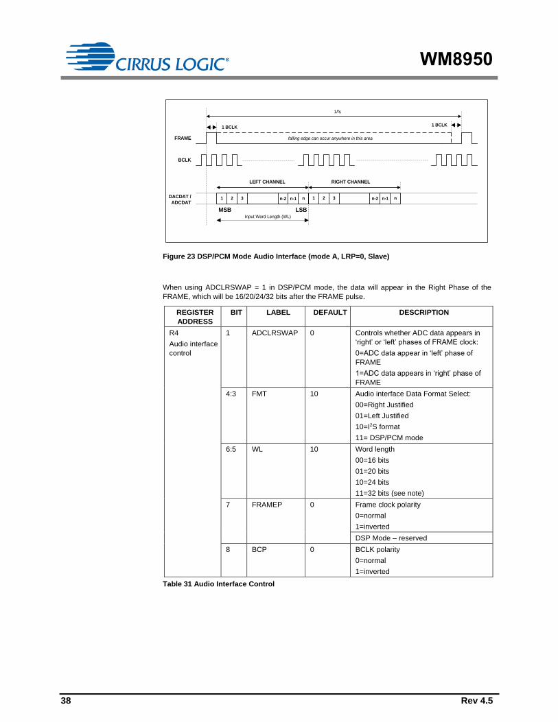
Figure 23 DSP/PCM Mode Audio Interface (mode A, LRP=0, Slave)
When using ADCLRSWAP = 1 in DSP/PCM mode, the data will appear in the Right Phase of the
FRAME, which will be 16/20/24/32 bits after the FRAME pulse.
REGISTER
ADDRESS
BIT LABEL DEFAULT DESCRIPTION
R4
Audio interface
control
1 ADCLRSWAP 0 Controls whether ADC data appears in
‘right’ or ‘left’ phases of FRAME clock:
0=ADC data appear in ‘left’ phase of
FRAME
1=ADC data appears in ‘right’ phase of
FRAME
4:3 FMT 10 Audio interface Data Format Select:
00=Right Justified
01=Left Justified
10=I2S format
11= DSP/PCM mode
6:5 WL 10 Word length
00=16 bits
01=20 bits
10=24 bits
11=32 bits (see note)
7 FRAMEP 0 Frame clock polarity
0=normal
1=inverted
DSP Mode – reserved
8 BCP 0 BCLK polarity
0=normal
1=inverted
Table 31 Audio Interface Control

WM8950
Rev 4.5 39
AUDIO INTERFACE CONTROL
The register bits controlling audio format, word length and master / slave mode are summarised
below. Each audio interface can be controlled individually.
Register bit MS selects audio interface operation in master or slave mode. In Master mode BCLK,
and FRAME are outputs. The frequency of BCLK and FRAME in master mode are controlled with
BCLKDIV. These are divided down versions of master clock. This may result in short BCLK pulses at
the end of a frame if there is a non-integer ratio of BCLKs to FRAME clocks.
REGISTER
ADDRESS
BIT LABEL DEFAULT DESCRIPTION
R6
Clock
generation
control
0 MS 0 Sets the chip to be master over FRAME
and BCLK
0=BCLK and FRAME clock are inputs
1=BCLK and FRAME clock are outputs
generated by the WM8950 (MASTER)
4:2 BCLKDIV 000 Configures the BCLK and FRAME output
frequency, for use when the chip is master
over BCLK.
000=divide by 1 (BCLK=MCLK)
001=divide by 2 (BCLK=MCLK/2)
010=divide by 4
011=divide by 8
100=divide by 16
101=divide by 32
110=reserved
111=reserved
7:5 MCLKDIV 010 Sets the scaling for either the MCLK or
PLL clock output (under control of
CLKSEL)
000=divide by 1
001=divide by 1.5
010=divide by 2
011=divide by 3
100=divide by 4
101=divide by 6
110=divide by 8
111=divide by 12
8 CLKSEL 1 Controls the source of the clock for all
internal operation:
0=MCLK
1=PLL output
Table 32 Clock Control
COMPANDING
The WM8950 supports A-law and -law companding. Companding can be enabled on the ADC
audio interface by writing the appropriate value to the ADC_COMP register bit.
REGISTER
ADDRESS
BIT LABEL DEFAULT DESCRIPTION
R5
Companding
control
2:1 ADC_COMP 0 ADC companding
00=off
01=reserved
10=µ-law
11=A-law
Table 33 Companding Control

WM8950
40 Rev 4.5
Companding involves using a piecewise linear approximation of the following equations (as set out
by ITU-T G.711 standard) for data compression:
-law (where =255 for the U.S. and Japan):
F(x) = ln(1 + |x|) / ln(1 + ) -1 ≤ x ≤ 1
A-law (where A=87.6 for Europe):
F(x) = A|x| / (1 + lnA) for x ≤ 1/A
F(x) = (1 + lnA|x|) / (1 + lnA) for 1/A ≤ x ≤ 1
The companded data is also inverted as recommended by the G.711 standard (all 8 bits are inverted
for -law, all even data bits are inverted for A-law). The data will be transmitted as the first 8 MSB’s
of data.
Companding converts 13 bits (-law) or 12 bits (A-law) to 8 bits using non-linear quantization. The
input data range is separated into 8 levels, allowing low amplitude signals better precision than that
of high amplitude signals. This is to exploit the operation of the human auditory system, where louder
sounds do not require as much resolution as quieter sounds. The companded signal is an 8-bit word
containing sign (1-bit), exponent (3-bits) and mantissa (4-bits).
BIT7 BIT[6:4] BIT[3:0]
SIGN EXPONENT MANTISSA
Table 34 8-bit Companded Word Composition
u-law Companding
0
20
40
60
80
100
120
0 0.1 0.2 0.3 0.4 0.5 0.6 0.7 0.8 0.9 1
Normalised Input
Co
mp
an
ded
Ou
tpu
t
0
0.1
0.2
0.3
0.4
0.5
0.6
0.7
0.8
0.9
1
No
rmali
sed
Ou
tpu
t
Figure 24 u-Law Companding

WM8950
Rev 4.5 41
A-law Companding
0
20
40
60
80
100
120
0 0.2 0.4 0.6 0.8 1
Normalised Input
Co
mp
an
ded
Ou
tpu
t
0
0.1
0.2
0.3
0.4
0.5
0.6
0.7
0.8
0.9
1
No
rmali
sed
Ou
tpu
t
Figure 25 A-Law Companding
AUDIO SAMPLE RATES
The WM8950 sample rate for the ADC is set using the SR register bits. The cut-offs for the digital
filters and the ALC attack/decay times stated are determined using these values and assume a 256fs
master clock rate.
If a sample rate that is not explicitly supported by the SR register settings is required then the closest
SR value to that sample rate should be chosen, the filter characteristics and the ALC attack, decay
and hold times will scale appropriately.
REGISTER
ADDRESS
BIT LABEL DEFAULT DESCRIPTION
R7
Additional
control
3:1 SR
000 Approximate sample rate (configures the
coefficients for the internal digital filters):
000=48kHz
001=32kHz
010=24kHz
011=16kHz
100=12kHz
101=8kHz
110-111=reserved
Table 35 Sample Rate Control

WM8950
42 Rev 4.5
MASTER CLOCK AND PHASE LOCKED LOOP (PLL)
The WM8950 has an on-chip phase-locked loop (PLL) circuit that can be used to:
Generate master clocks for the WM8950 audio functions from another external clock, e.g. in
telecoms applications.
Generate and output (on pin CSB/GPIO) a clock for another part of the system that is derived from an
existing audio master clock.
Figure 26 shows the PLL and internal clocking arrangement on the WM8950.
The PLL can be enabled or disabled by the PLLEN register bit.
REGISTER
ADDRESS
BIT LABEL DEFAULT DESCRIPTION
R1
Power
management 1
5 PLLEN 0 PLL enable
0=PLL off
1=PLL on
Table 36 PLLEN Control Bit
MCLK
f/2
PLL1
R=f2/f
1
f/4
256fs
CSB/GPIO
f2
f1
GPIOSEL
R8[2:1]
...
PLLPRESCALE
R36[4]
f/N
MCLKDIV
R6[7:5]
OPCLKDIV
R8[5:4]
f/N
ADC
f/4
MASTER
MODE
ADCOSR128
R14[3]
FRAME
BCLK
CLKSEL
R6[8]
f/2
BCLKDIV
R6[4:2]
MS
R6[0]
MS
R6[0]
fPLLOUT
Figure 26 PLL and Clock Select Circuit
The PLL frequency ratio R = f2/f1 (see Figure 26) can be set using the register bits PLLK and PLLN:
PLLN = int R
PLLK = int (224 (R-PLLN))
EXAMPLE:
MCLK=12MHz, required clock = 12.288MHz.
R should be chosen to ensure 5 < PLLN < 13. There is a fixed divide by 4 in the PLL and a selectable
divide by N after the PLL which should be set to divide by 2 to meet this requirement.
Enabling the divide by 2 sets the required f2 = 4 x 2 x 12.288MHz = 98.304MHz.
R = 98.304 / 12 = 8.192
PLLN = int R = 8
k = int ( 224 x (8.192 – 8)) = 3221225 = 3126E9h

WM8950
Rev 4.5 43
REGISTER
ADDRESS
BIT LABEL DEFAULT DESCRIPTION
R36
PLL N value
4 PLLPRESCALE 0 0 = MCLK input not divided (default)
1 = Divide MCLK by 2 before input to
PLL
3:0 PLLN 1000 Integer (N) part of PLL input/output
frequency ratio. Use values greater
than 5 and less than 13.
R37
PLL K value 1
5:0 PLLK [23:18] 0Ch Fractional (K) part of PLL1
input/output frequency ratio (treat as
one 24-digit binary number). R38
PLL K Value 2
8:0 PLLK [17:9] 093h
R39
PLL K Value 3
8:0 PLLK [8:0] 0E9h
Table 37 PLL Frequency Ratio Control
The PLL performs best when f2 is around 90MHz. Its stability peaks at N=8. Some example settings
are shown in Figure 35.
MCLK
(MHz)
(F1)
DESIRED
OUTPUT
(MHz)
F2
(MHz)
PRESCALE
DIVIDE
POSTSCALE
DIVIDE
R N
(Hex)
K
(Hex)
12 11.2896 90.3168 1 2 7.5264 7 86C220
12 12.288 98.304 1 2 8.192 8 3126E8
13 11.2896 90.3168 1 2 6.947446 6 F28BD4
13 12.288 98.304 1 2 7.561846 7 8FD525
14.4 11.2896 90.3168 1 2 6.272 6 45A1CA
14.4 12.288 98.304 1 2 6.826667 6 D3A06E
19.2 11.2896 90.3168 2 2 9.408 9 6872AF
19.2 12.288 98.304 2 2 10.24 A 3D70A3
19.68 11.2896 90.3168 2 2 9.178537 9 2DB492
19.68 12.288 98.304 2 2 9.990243 9 FD809F
19.8 11.2896 90.3168 2 2 9.122909 9 1F76F7
19.8 12.288 98.304 2 2 9.929697 9 EE009E
24 11.2896 90.3168 2 2 7.5264 7 86C226
24 12.288 98.304 2 2 8.192 8 3126E8
26 11.2896 90.3168 2 2 6.947446 6 F28BD4
26 12.288 98.304 2 2 7.561846 7 8FD525
27 11.2896 90.3168 2 2 6.690133 6 BOAC93
27 12.288 98.304 2 2 7.281778 7 482296
Table 38 PLL Frequency Examples

WM8950
44 Rev 4.5
GENERAL PURPOSE INPUT/OUTPUT
The CSB/GPIO pin can be configured to perform a variety of useful tasks by setting the GPIOSEL
register bits. The GPIO is only available in 2 wire mode.
REGISTER
ADDRESS
BIT LABEL DEFAULT DESCRIPTION
R8
GPIO
control
2:0 GPIOSEL 000 CSB/GPIO pin function select:
000=CSB input
001=Reserved
010=Temp ok
011=Automute active
100=PLL clk o/p
101=PLL lock
110=Reserved
111=Reserved
3 GPIOPOL 0 GPIO Polarity invert
0=Non inverted
1=Inverted
5:4 OPCLKDIV 00 PLL Output clock division ratio
00=divide by 1
01=divide by 2
10=divide by 3
11=divide by 4
Table 39 CSB/GPIO Control
CONTROL INTERFACE
SELECTION OF CONTROL MODE AND 2-WIRE MODE ADDRESS
The control interface can operate as either a 3-wire or 2-wire MPU interface. The MODE pin
determines the 2 or 3 wire mode as shown in Table 40.
The WM8950 is controlled by writing to registers through a serial control interface. A control word
consists of 16 bits. The first 7 bits (B15 to B9) are address bits that select which control register is
accessed. The remaining 9 bits (B8 to B0) are register bits, corresponding to the 9 bits in each
control register.
MODE INTERFACE FORMAT
Low 2 wire
High 3 wire
Table 40 Control Interface Mode Selection
3-WIRE SERIAL CONTROL MODE
In 3-wire mode, every rising edge of SCLK clocks in one data bit from the SDIN pin. A rising edge on
CSB/GPIO latches in a complete control word consisting of the last 16 bits.
B15 B14 B13 B12 B11 B10 B9 B8 B7 B6 B5 B4 B3 B2 B1 B0SDIN
SCLK
CSB
control register address control register data bits
latch
Figure 27 3-Wire Serial Control Interface

WM8950
Rev 4.5 45
2-WIRE SERIAL CONTROL MODE
The WM8950 supports software control via a 2-wire serial bus. Many devices can be controlled by
the same bus, and each device has a unique 7-bit device address (this is not the same as the 7-bit
address of each register in the WM8950).
The WM8950 operates as a slave device only. The controller indicates the start of data transfer with
a high to low transition on SDIN while SCLK remains high. This indicates that a device address and
data will follow. All devices on the 2-wire bus respond to the start condition and shift in the next eight
bits on SDIN (7-bit address + Read/Write bit, MSB first). If the device address received matches the
address of the WM8950, then the WM8950 responds by pulling SDIN low on the next clock pulse
(ACK). If the address is not recognised or the R/W bit is ‘1’ when operating in write only mode, the
WM8950 returns to the idle condition and wait for a new start condition and valid address.
During a write, once the WM8950 has acknowledged a correct address, the controller sends the first
byte of control data (B15 to B8, i.e. the WM8950 register address plus the first bit of register data).
The WM8950 then acknowledges the first data byte by pulling SDIN low for one clock pulse. The
controller then sends the second byte of control data (B7 to B0, i.e. the remaining 8 bits of register
data), and the WM8950 acknowledges again by pulling SDIN low.
Transfers are complete when there is a low to high transition on SDIN while SCLK is high. After a
complete sequence the WM8950 returns to the idle state and waits for another start condition. If a
start or stop condition is detected out of sequence at any point during data transfer (i.e. SDIN
changes while SCLK is high), the device jumps to the idle condition.
SDIN
SCLK
register address and1st register data bit
DEVICE ADDRESS(7 BITS)
RD / WRBIT
ACK(LOW)
CONTROL BYTE 1(BITS 15 TO 8)
CONTROL BYTE 1(BITS 7 TO 0)
remaining 8 bits ofregister data
STOPSTART
ACK(LOW)
ACK(LOW)
Figure 28 2-Wire Serial Control Interface
In 2-wire mode the WM8950 has a fixed device address, 0011010.
RESETTING THE CHIP
The WM8950 can be reset by performing a write of any value to the software reset register (address
0 hex). This will cause all register values to be reset to their default values. In addition to this there
is a Power-On Reset (POR) circuit which ensures that the registers are set to default when the device
is powered up.

WM8950
46 Rev 4.5
POWER SUPPLIES
The WM8950 can use up to three separate power supplies:
AVDD, AVDD2, AGND and AGND2: Analogue supply, powers all analogue functions. AVDD can
range from 2.5V to 3.6V and has the most significant impact on overall power consumption. A large
AVDD slightly improves audio quality.
DCVDD: Digital core supply, powers all digital functions except the audio and control interfaces.
DCVDD can range from 1.71V to 3.6V, and has no effect on audio quality. The return path for
DCVDD is DGND, which is shared with DBVDD.
DBVDD Can range from 1.71V to 3.6V. DBVDD return path is through DGND.
It is possible to use the same supply voltage for all supplies. However, digital and analogue supplies
should be routed and decoupled separately on the PCB to keep digital switching noise out of the
analogue signal paths.
ADC POWER UP/DOWN SEQUENCE
Vpora
DGND
Internal POR active
Device ReadyNo Power
Vpor_off
Power Supply
POR
I2S Clocks
ADC Internal
State
tmidrail_on
Analogue Inputs
ADCDAT pin
GD
ADCEN bit
Power down Init Normal Operation Normal OperationInitPD Power down
ADC enabled ADC enabledADC off
tadcint
DNC
INPPGAEN bit
tadcint
INPPGA enabled
DNC
GD GD GD
PORPOR Undefined
VMID enabled
VMIDSEL/
BIASEN bits
AVDD/2
tmidrail_off
(Note 1) (Note 2)
(Note 3)
(Note 4)
Vpor_on
Figure 29 ADC Power Up and Down Sequence (not to scale)
SYMBOL MIN TYPICAL MAX UNIT
tmidrail_on 500 ms
tmidrail_off >10 s
tadcint 2/fs n/fs
Table 41 Typical POR Operation (typical values, not tested)
Notes:

WM8950
Rev 4.5 47
1. The analogue input pin charge time, tmidrail_on, is determined by the VMID pin charge time. This
time is dependent upon the value of VMID decoupling capacitor and VMID pin input resistance
and AVDD power supply rise time.
2. The analogue input pin discharge time, tmidrail_off, is determined by the analogue input coupling
capacitor discharge time. The time, tmidrail_off, is measured using a 1μF capacitor on the analogue
input but will vary dependent upon the value of input coupling capacitor.
3. While the ADC is enabled there will be LSB data bit activity on the ADCDAT pin due to system
noise but no significant digital output will be present.
4. The VMIDSEL and BIASEN bits must be set to enable analogue input midrail voltage and for
normal ADC operation.
5. ADCDAT data output delay from power up - with power supplies starting from 0V - is determined
primarily by the VMID charge time. ADC initialisation and power management bits may be set
immediately after POR is released; VMID charge time will be significantly longer and will dictate
when the device is stabilised for analogue input.
6. ADCDAT data output delay at power up from device standby (power supplies already applied) is
determined by ADC initialisation time, 2/fs.
POWER MANAGEMENT
SAVING POWER BY REDUCING OVERSAMPLING RATE
The default mode of operation of the ADC digital filters is in 64x oversampling mode. Under the
control of ADCOSR the oversampling rate may be doubled. 64x oversampling results in a slight
decrease in noise performance compared to 128x but lowers the power consumption of the device.
REGISTER
ADDRESS
BIT LABEL DEFAULT DESCRIPTION
R14
ADC control
3 ADCOSR128 0 ADC oversample rate select
0 = 64x (lowest power)
1 = 128x (best SNR)
Table 42 ADC Oversampling Rate Selection
VMID
The analogue circuitry will not work unless VMID is enabled (VMIDSEL≠00). The impedance of the
VMID resistor string, together with the decoupling capacitor on the VMID pin will determine the start-
up time of the VMID circuit.
REGISTER
ADDRESS
BIT LABEL DEFAULT DESCRIPTION
R1
Power
management 1
1:0 VMIDSEL 00 Reference string impedance to VMID pin
(determines start-up time):
00=off (open circuit)
01=50kΩ
10=500kΩ
11=5kΩ (for fastest start-up)
Table 43 VMID Impedance Control
BIASEN
REGISTER
ADDRESS
BIT LABEL DEFAULT DESCRIPTION
R1
Power
management 1
3 BIASEN 0 Analogue amplifier bias control
Table 44 BIASEN Control

WM8950
48 Rev 4.5
ESTIMATED SUPPLY CURRENTS
When the ADC is enabled it is estimated that approximately 4mA will be drawn from DCVDD when
DCVDD=1.8V and fs=48kHz. (This will be lower at lower sample rates). When the PLL is enabled an
additional 700 microamps will be drawn from DCVDD.
Table 59 shows the estimated 3.3V AVDD current drawn by various circuits, by register bit.
REGISTER BIT AVDD CURRENT (MILLIAMPS)
PLLEN 1.4 (with clocks applied)
MICBEN 0.5
BIASEN 0.3
BUFIOEN 0.1
VMIDSEL 10K=>0.3, less than 0.1 for 50k/500k
INPPGAEN 0.2
ADCEN x64 (ADCOSR=0)=>2.6, x128 (ADCOSR=1)=>4.9
Table 45 AVDD Supply Current

WM8950
Rev 4.5 49
REGISTER MAP
ADDR
B[15:9]
REGISTER
NAME
B8 B7 B6 B5 B4 B3 B2 B1 B0 DEF’T
VAL
DEC HEX (HEX)
0 00 Software Reset Software reset
1 01 Power manage’t
1
0 0 AUXEN PLLEN MICBEN BIASEN BUFIOEN VMIDSEL 000
2 02 Power manage’t
2
0 0 0 0 BOOSTEN 0 INPPGAEN 0 ADCEN 000
4 04 Audio Interface BCP FRAMEP WL FMT 0 ALRSWAP 0 050
5 05 Companding ctrl 0 0 0 0 0 ADC_COMP 0 000
6 06 Clock Gen ctrl CLKSEL MCLKDIV BCLKDIV 0 MS 140
7 07 Additional ctrl 0 0 0 0 0 SR SLOWCLK
EN
000
8 08 GPIO Stuff 0 0 0 OPCLKDIV GPIOPOL GPIOSEL 000
14 0E ADC Control HPFEN HPFAPP HPFCUT ADCOSR
128
0 0 ADCPOL 100
15 0F ADC Digital Vol 0 ADCVOL 0FF
18 12 EQ1 – low shelf 0 0 EQ1C EQ1G 12C
19 13 EQ2 – peak 1 EQ2BW 0 EQ2C EQ2G 02C
20 14 EQ3 – peak 2 EQ3BW 0 EQ3C EQ3G 02C
21 15 EQ4 – peak 3 EQ4BW 0 EQ4C EQ4G 02C
22 16 EQ5 – high
shelf
0 0 EQ5C EQ5G 02C
27 1B Notch Filter 1 NFU NFEN NFA0[13:7] 000
28 1C Notch Filter 2 NFU 0 NFA0[6:0] 000
29 1D Notch Filter 3 NFU 0 NFA1[13:7] 000
30 1E Notch Filter 4 NFU 0 NFA1[6:0] 000
32 20 ALC control 1 ALCSEL 0 0 ALCMAX ALCMIN 038
33 21 ALC control 2 ALCZC ALCHLD ALCLVL 00B
34 22 ALC control 3 ALCMODE ALCDCY ALCATK 032
35 23 Noise Gate 0 0 0 0 0 NGEN NGTH 000
36 24 PLL N 0 0 0 0 PLL_PRE
SCALE
PLLN[3:0] 008
37 25 PLL K 1 0 0 0 PLLK[23:18] 00C
38 26 PLL K 2 PLLK[17:9] 093
39 27 PLL K 3 PLLK[8:0] 0E9
44 2C Input ctrl MBVSEL 0 0 0 0 AUXMODE AUX2
INPPGA
MICN2
INPPGA
MICP2
INPPGA
003
45 2D INP PGA gain
ctrl
0 INPPGAZC INPPGA
MUTE
INPPGAVOL 010
47 2F ADC Boost ctrl PGABOOST 0 MICP2BOOSTVOL 0 AUX2BOOSTVOL 100
49 31 Thermal
Shutdown
0 0 0 0 0 0 0 TSDEN 0 002

WM8950
50 Rev 4.5
DIGITAL FILTER CHARACTERISTICS
PARAMETER TEST CONDITIONS MIN TYP MAX UNIT
ADC Filter
Passband +/- 0.025dB 0 0.454fs
-6dB 0.5fs
Passband Ripple +/- 0.025 dB
Stopband 0.546fs
Stopband Attenuation f > 0.546fs -60 dB
Group Delay 21/fs
ADC High-Pass Filter
High-Pass Filter Corner
Frequency
-3dB 3.7 Hz
-0.5dB 10.4
-0.1dB 21.6
Table 46 Digital Filter Characteristics
TERMINOLOGY
1. Stop Band Attenuation (dB) – the degree to which the frequency spectrum is attenuated (outside audio band)
2. Pass-band Ripple – any variation of the frequency response in the pass-band region
3. Note that this delay applies only to the filters and does not include additional delays through other digital circuits. See
Table 47 for the total delay.
PARAMETER TEST CONDITIONS MIN TYP MAX UNIT
ADC Path Group Delay
Total Delay (ADC analogue
input to digital audio interface
output)
EQ disabled 26/fs 28/fs 30/fs
EQ enabled 27/fs 29/fs 31/fs
Table 47 Total Group Delay
Note: Wind noise filter is disabled.
ADC FILTER RESPONSES
-120
-100
-80
-60
-40
-20
0
0 0.5 1 1.5 2 2.5 3
Frequency (Fs)
Response (
dB
)
-0.2
-0.15
-0.1
-0.05
0
0.05
0.1
0.15
0.2
0 0.1 0.2 0.3 0.4 0.5
Frequency (Fs)
Response (
dB
)
Figure 30 ADC Digital Filter Frequency Response Figure 31 ADC Digital Filter Ripple

WM8950
Rev 4.5 51
DE-EMPHASIS FILTER RESPONSES
-10
-9
-8
-7
-6
-5
-4
-3
-2
-1
0
0 2000 4000 6000 8000 10000 12000 14000 16000
Frequency (Hz)
Response (
dB
)
-0.15
-0.10
-0.05
0.00
0.05
0.10
0.15
0.20
0.25
0.30
0 2000 4000 6000 8000 10000 12000 14000 16000
Frequency (Hz)
Response (
dB
)
Figure 32 De-emphasis Frequency Response (32kHz) Figure 33 De-emphasis Error (32kHz)
-10
-9
-8
-7
-6
-5
-4
-3
-2
-1
0
0 5000 10000 15000 20000
Frequency (Hz)
Response (
dB
)
-0.20
-0.15
-0.10
-0.05
0.00
0.05
0.10
0 5000 10000 15000 20000
Frequency (Hz)
Response (
dB
)
Figure 34 De-emphasis Frequency Response (44.1kHz) Figure 35 De-emphasis Error (44.1kHz)
-10
-9
-8
-7
-6
-5
-4
-3
-2
-1
0
0 5000 10000 15000 20000
Frequency (Hz)
Response (
dB
)
-0.10
-0.08
-0.06
-0.04
-0.02
0.00
0.02
0.04
0.06
0.08
0.10
0 5000 10000 15000 20000
Frequency (Hz)
Response (
dB
)
Figure 36 De-emphasis Frequency Response (48kHz) Figure 37 De-emphasis Error (48kHz)

WM8950
52 Rev 4.5
HIGH-PASS FILTER
The WM8950 has a selectable digital high-pass filter in the ADC filter path. This filter has two
modes, audio and applications. In audio mode the filter is a 1st order IIR with a cut-off of around
3.7Hz. In applications mode the filter is a 2nd order high-pass filter with a selectable cut-off
frequency.
-40
-35
-30
-25
-20
-15
-10
-5
0
5
0 5 10 15 20 25 30 35 40 45
Frequency (Hz)
Response (
dB
)
-60
-50
-40
-30
-20
-10
0
10
0 200 400 600 800 1000 1200
Frequency (Hz)
Re
sp
on
se
(d
B)
Figure 38 ADC High-pass Filter Response, HPFAPP=0 Figure 39 ADC High-pass Filter Responses (48kHz),
HPFAPP=1, all cut-off settings shown.
-80
-70
-60
-50
-40
-30
-20
-10
0
10
0 200 400 600 800 1000 1200
Frequency (Hz)
Response (
dB
)
-90
-80
-70
-60
-50
-40
-30
-20
-10
0
10
0 200 400 600 800 1000 1200
Frequency (Hz)
Response (
dB
)
Figure 40 ADC High-pass Filter Responses (24kHz),
HPFAPP=1, all cut-off settings shown.
Figure 41 ADC High-pass Filter Responses (12kHz),
HPFAPP=1, all cut-off settings shown.

WM8950
Rev 4.5 53
5-BAND EQUALISER
The WM8950 has a 5-band equaliser which can be applied to the ADC path. The plots from Figure
42 to Figure 55 show the frequency responses of each filter with a sampling frequency of 48kHz,
firstly showing the different cut-off/centre frequencies with a gain of 12dB, and secondly a sweep of
the gain from -12dB to +12dB for the lowest cut-off/centre frequency of each filter.
10-1
100
101
102
103
104
105
-15
-10
-5
0
5
10
15
Frequency (Hz)
Magnitude (
dB
)
10-1
100
101
102
103
104
105
-15
-10
-5
0
5
10
15
Frequency (Hz)M
agnitude (
dB
)
Figure 42 EQ Band 1 – Low Frequency Shelf Filter Cut-offs Figure 43 EQ Band 1 – Gains for Lowest Cut-off Frequency
10-1
100
101
102
103
104
105
-15
-10
-5
0
5
10
15
Frequency (Hz)
Magnitude (
dB
)
10-1
100
101
102
103
104
105
-15
-10
-5
0
5
10
15
Frequency (Hz)
Magnitude (
dB
)
Figure 44 EQ Band 2 – Peak Filter Centre Frequencies,
EQ2BW=0
Figure 45 EQ Band 2 – Peak Filter Gains for Lowest Cut-off
Frequency, EQ2BW=0
10-2
10-1
100
101
102
103
104
-15
-10
-5
0
5
10
15
Frequency (Hz)
Magnitude (
dB
)
Figure 46 EQ Band 2 – EQ2BW=0, EQ2BW=1

WM8950
54 Rev 4.5
10-1
100
101
102
103
104
105
-15
-10
-5
0
5
10
15
Frequency (Hz)
Magnitude (
dB
)
10-1
100
101
102
103
104
105
-15
-10
-5
0
5
10
15
Frequency (Hz)
Magnitude (
dB
)
Figure 47 EQ Band 3 – Peak Filter Centre Frequencies,
EQ3BW=0
Figure 48 EQ Band 3 – Peak Filter Gains for Lowest Cut-off
Frequency, EQ3BW=0
10-2
10-1
100
101
102
103
104
-15
-10
-5
0
5
10
15
Frequency (Hz)
Magnitude (
dB
)
Figure 49 EQ Band 3 – EQ3BW=0, EQ3BW=1

WM8950
Rev 4.5 55
10-1
100
101
102
103
104
105
-15
-10
-5
0
5
10
15
Frequency (Hz)
Magnitude (
dB
)
10-1
100
101
102
103
104
105
-15
-10
-5
0
5
10
15
Frequency (Hz)
Magnitude (
dB
)
Figure 50 EQ Band 4 – Peak Filter Centre Frequencies,
EQ3BW=0
Figure 51 EQ Band 4 – Peak Filter Gains for Lowest Cut-off
Frequency, EQ4BW=0
10-2
10-1
100
101
102
103
104
-15
-10
-5
0
5
10
15
Frequency (Hz)
Magnitude (
dB
)
Figure 52 EQ Band 4 – EQ3BW=0, EQ3BW=1
10-1
100
101
102
103
104
105
-15
-10
-5
0
5
10
15
Frequency (Hz)
Magnitude (
dB
)
10-1
100
101
102
103
104
105
-15
-10
-5
0
5
10
15
Frequency (Hz)
Magnitude (
dB
)
Figure 53 EQ Band 5 – High Frequency Shelf Filter Cut-offs Figure 54 EQ Band 5 – Gains for Lowest Cut-off Frequency

WM8950
56 Rev 4.5
Figure 55 shows the result of having the gain set on more than one channel simultaneously. The
blue traces show each band (lowest cut-off/centre frequency) with 12dB gain. The red traces show
the cumulative effect of all bands with +12dB gain and all bands -12dB gain, with EQxBW=0 for the
peak filters.
10-1
100
101
102
103
104
105
-15
-10
-5
0
5
10
15
20
Frequency (Hz)
Magnitude (
dB
)
Figure 55 Cumulative Frequency Boost/Cut

WM8950
Rev 4.5 57
APPLICATIONS INFORMATION
RECOMMENDED EXTERNAL COMPONENTS
WM8950
DNC
DNC
DNC
TP
AVDD2AGND2
Notes:
1. AGND and DGND should be connected as close to the WM8950 as possible.
2. C1, C2, C3, C4, C8 and C9 should be positioned as close to WM8950 as possible.
3. Capacitor types should be carefully chosen. Capacitors with very low ESR are recommended for optimum performance.
4. R3 can be populated with other values to remove common mode noise on the microphone.
5. For added strength and heat dissipation, it is recommended that the GND_PADDLE (Pin 25) is connected to AGND.
AVDDDCVDD
DBVDD
ADCDAT
FRAMEBCLKMCLK
AUX
VMID
MICBIAS
MICPMICN GND_PADDLE
SDINSCLK
CSB/GPIO
MODE
DGNDAGND
Figure 56 Recommended External Components

WM8950
58 Rev 4.5
PACKAGE DIAGRAM
DM102.CFL: 24 PIN QFN PLASTIC PACKAGE 4 X 4 X 0.9 mm BODY, 0.50 mm LEAD PITCH
INDEX AREA
(D/2 X E/2)
TOP VIEW
D
E
4
NOTES:
1. DIMENSION b APPLIES TO METALLIZED TERMINAL AND IS MEASURED BETWEEN 0.15 mm AND 0.30 mm FROM TERMINAL TIP.
2. FALLS WITHIN JEDEC, MO-220, VARIATION VGGD-8.
3. ALL DIMENSIONS ARE IN MILLIMETRES.
4. THE TERMINAL #1 IDENTIFIER AND TERMINAL NUMBERING CONVENTION SHALL CONFORM TO JEDEC 95-1 SPP-002.
5. COPLANARITY APPLIES TO THE EXPOSED HEAT SINK SLUG AS WELL AS THE TERMINALS.
6. REFER TO APPLICATIONS NOTE WAN_0118 FOR FURTHER INFORMATION REGARDING PCB FOOTPRINTS AND QFN PACKAGE SOLDERING.
7. THIS DRAWING IS SUBJECT TO CHANGE WITHOUT NOTICE.
A3G
T
H
W
b
Exposed lead
Half etch tie bar
Dimensions (mm)Symbols
MIN NOM MAX NOTE
A
A1
A3
0.80 0.85 0.90
0.050.0350
0.203 REF
b
D
D2
E
E2
e
L
0.300.20
4.00 BSC
2.602.502.40
0.50 BSC
0.35 0.40 0.45
2
2
4.00 BSC
2.602.502.40
0.10
aaa
bbb
ccc
REF:
0.10
0.10
JEDEC, MO-220, VARIATION VGGD-8.
Tolerances of Form and Position
0.25
H 0.10
0.20G
T 0.103
W 0.15
DETAIL 1
DETAIL 3
6
1
13
18
2419
12
e
D2
b7 1
BCbbb M A
BOTTOM VIEW
Caaa2 X
Caaa2 X
1
C
A3
SEATING PLANE
A1
C0.08
Cccc
A
5
SIDE VIEW
EXPOSED
GROUND
PADDLE
6
DETAIL 1
0.30mm
45°
EXPOSED
GROUND
PADDLE
E2
SEE DETAIL 2
L
e
Datum
DETAIL 2
Terminal
Tip
e/2
1
M M DETAIL 3

WM8950
Rev 4.5 59
IMPORTANT NOTICE
Contacting Cirrus Logic Support For all product questions and inquiries, contact a Cirrus Logic Sales Representative.
To find one nearest you, go to www.cirrus.com.
For the purposes of our terms and conditions of sale, "Preliminary" or "Advanced" datasheets are non-final datasheets that
include but are not limited to datasheets marked as “Target”, “Advance”, “Product Preview”, “Preliminary Technical Data”
and/or “Pre-production.” Products provided with any such datasheet are therefore subject to relevant terms and conditions
associated with "Preliminary" or "Advanced" designations. The products and services of Cirrus Logic International (UK)
Limited; Cirrus Logic, Inc.; and other companies in the Cirrus Logic group (collectively either “Cirrus Logic” or “Cirrus”) are
sold subject to Cirrus Logic’s terms and conditions of sale supplied at the time of order acknowledgment, including those
pertaining to warranty, indemnification, and limitation of liability. Software is provided pursuant to applicable license terms.
Cirrus Logic reserves the right to make changes to its products and specifications or to discontinue any product or service
without notice. Customers should therefore obtain the latest version of relevant information from Cirrus Logic to verify that
the information is current and complete. Testing and other quality control techniques are utilized to the extent Cirrus Logic
deems necessary. Specific testing of all parameters of each device is not necessarily performed. In order to minimize risks
associated with customer applications, the customer must use adequate design and operating safeguards to minimize
inherent or procedural hazards. Cirrus Logic is not liable for applications assistance or customer product design. The
customer is solely responsible for its selection and use of Cirrus Logic products. Use of Cirrus Logic products may entail a
choice between many different modes of operation, some or all of which may require action by the user, and some or all of
which may be optional. Nothing in these materials should be interpreted as instructions or suggestions to choose one mode
over another. Likewise, description of a single mode should not be interpreted as a suggestion that other modes should not
be used or that they would not be suitable for operation. Features and operations described herein are for illustrative
purposes only.
CERTAIN APPLICATIONS USING SEMICONDUCTOR PRODUCTS MAY INVOLVE POTENTIAL RISKS OF DEATH,
PERSONAL INJURY, OR SEVERE PROPERTY OR ENVIRONMENTAL DAMAGE (“CRITICAL APPLICATIONS”). CIRRUS
LOGIC PRODUCTS ARE NOT DESIGNED, AUTHORIZED OR WARRANTED FOR USE IN PRODUCTS SURGICALLY
IMPLANTED INTO THE BODY, AUTOMOTIVE SAFETY OR SECURITY DEVICES, NUCLEAR SYSTEMS, LIFE
SUPPORT PRODUCTS OR OTHER CRITICAL APPLICATIONS. INCLUSION OF CIRRUS LOGIC PRODUCTS IN SUCH
APPLICATIONS IS UNDERSTOOD TO BE FULLY AT THE CUSTOMER’S RISK AND CIRRUS LOGIC DISCLAIMS AND
MAKES NO WARRANTY, EXPRESS, STATUTORY OR IMPLIED, INCLUDING THE IMPLIED WARRANTIES OF
MERCHANTABILITY AND FITNESS FOR PARTICULAR PURPOSE, WITH REGARD TO ANY CIRRUS LOGIC PRODUCT
THAT IS USED IN SUCH A MANNER. IF THE CUSTOMER OR CUSTOMER’S CUSTOMER USES OR PERMITS THE
USE OF CIRRUS LOGIC PRODUCTS IN CRITICAL APPLICATIONS, CUSTOMER AGREES, BY SUCH USE, TO FULLY
INDEMNIFY CIRRUS LOGIC, ITS OFFICERS, DIRECTORS, EMPLOYEES, DISTRIBUTORS AND OTHER AGENTS
FROM ANY AND ALL LIABILITY, INCLUDING ATTORNEYS’ FEES AND COSTS, THAT MAY RESULT FROM OR ARISE
IN CONNECTION WITH THESE USES.
This document is the property of Cirrus Logic and by furnishing this information, Cirrus Logic grants no license, express or
implied, under any patents, mask work rights, copyrights, trademarks, trade secrets or other intellectual property rights. Any
provision or publication of any third party’s products or services does not constitute Cirrus Logic’s approval, license,
warranty or endorsement thereof. Cirrus Logic gives consent for copies to be made of the information contained herein only
for use within your organization with respect to Cirrus Logic integrated circuits or other products of Cirrus Logic, and only if
the reproduction is without alteration and is accompanied by all associated copyright, proprietary and other notices and
conditions (including this notice). This consent does not extend to other copying such as copying for general distribution,
advertising or promotional purposes, or for creating any work for resale. This document and its information is provided “AS
IS” without warranty of any kind (express or implied). All statutory warranties and conditions are excluded to the fullest
extent possible. No responsibility is assumed by Cirrus Logic for the use of information herein, including use of this
information as the basis for manufacture or sale of any items, or for infringement of patents or other rights of third parties.
Cirrus Logic, Cirrus, the Cirrus Logic logo design, and SoundClear are among the trademarks of Cirrus Logic. Other brand
and product names may be trademarks or service marks of their respective owners.
Copyright © 2005–2016 Cirrus Logic, Inc. All rights reserved.

WM8950
60 Rev 4.5
REVISION HISTORY
DATE REV ORIGINATOR CHANGES
26/09/11 4.4 JMacD Order codes changed from WM8950GEFL/V and WM8950GEFL/RV to
WM8950CGEFL/V and WM8950CGEFL/RV to reflect change to copper wire
bonding.
26/09/11 4.4 JMacD Package diagram changed to DM102.C
12/08/16 4.5 PH MICBIAS voltage (MBVSEL=1) updated to 0.75 x AVDD.
System clock timing requirements updated.