ERFM: How to understand customer engagement better than ever

AD-A255 836WL-TR-92-3015 !HlllllI~l~llm
ELECTRONICS RELIABILITY FRACTURE MECHANICS
VOLUME 1. CAUSES OF FAILURES OF SHOP REPLACEABLEUNITS AND HYBRID MICROCIRCUITS
J. Kallis, D. Buechler, J. Erickson,D. Van Westerhuyzen, R. Stokes, R. Ritacco,C. Spruck, T. Draper, T. Preston, W. Kusumoto,Z. Richardson, S. Lopez, K. Scott, P. Backes,B. Steffan, H. Ogomori, D. Grantham, M. Norris
Hughes Aircraft CompanyP. O. Box 902El Segundo, California 90245
May 1992
Final Report for Period May 1987 - September 1991
APPROVED FOR PUBLIC RELEASE;DISTRIBUTION 1 UNIMITED
FLIGHT DYNAMICS DIRECTORATEWRIGHT LABORATORYWRIGHT-PATTERSON AIR FORCE BASE, OHIO 45433-6553

S
NOTICE
When Government drawings, specifications, or other data are used for any purpose other than
in connection with a definitely Government-related procurement, the United States Governmentincurs no responsibility or any obligation whatsoever. The fact that the government may haveformulated or in any way supplied the said drawings, specifications, or other data, is not to beregarded by implication, or otherwise in any manner construed, as licensing the holder, or any
other person or corporation; or as conveying any rights or permission to manufacture, use, or sellany patented invention that may in any way be related thereto.
This report is releasable to the National Technical Information Service (NTIS). At NTIS, it
will be available to the general public, including foreign nations.This technical report has been reviewed and is approved for publication.
ALAN H. BURKHARD ALBERT R. BASSO, II, CM
Project Engineer Chief, Environmental Control BranchEnvironmental Control Branch Vehicle Subsystems Division
RICHARD E. COLCLUXChief
Vehicle Subsystems Division
If your address has changed, if you wish to be removed from our mailing list, or if the
addressee is no longer employed by your organization please notify WL/FIVE, WPAFB, OH45433-6553 to help us maintain a current mailing list.
Copies of this report should not be returned unless return is required by security
considerations, contractual obligations, or notice on a specific document.

UNCLASSIFIED
SECURITY CLASSIFICATION OF THIS PAGEForm Approved
REPORT DOCUMENTATION PAGE OW No. 070,HB
Is. REPORT SECURITY CLASSIFICATION lb. RESTRICTIVE MARKINGSUNCLASSIFIED
2a. SECURITY CLASSIFICATION AUTHORITY 3. DISTRIBUTION/AVAILABILITY OF REPORT
2b. DECLASSIFICATION/DOWNGRADING SCHEDULE Approved for public release; distribution is unlimited.
4. PERFORMING ORGANIZATION REPORT NUMBER(S) 5. MONITORING ORGANIZATION REPORT NUMBER(S)EDSG Report R160309 WL-TR-92-3015
6a. NAME OF PERFORMING ORGANIZATION 6b. OFFICE SYMBOL 7&, NAME OF MONITORING ORGANIZATION
HeAiy( ) Flight Dynamics Directorate (WIFIVE)Hughes Aircraft Company Wright Laboratory
6c. ADDRESS (Ci4, State, and ZIP Code) 7b. ADDRESS(City, State, and ZIP Code)P.O. Box 902 Wright-Patterson AFB, OH 45433-6553El Segundo, CA 90245
8a. NAME OF FUNDING/SPONSORING eIb. OFFICE SYMBOL 9. PROCUREMENT INSTRUMENT IDENTIFICATION NUMBERORGANIZATION (If appicabi.)Flight Dynamics Directorate WI/FIVE Contract No. F33615-87-C-3403
8c. ADDRESS (City, State, and ZIP Code) 10. SOURCE OF FUNDING NUMBERSPROGRAM PROJECT NO. I TASK NO. WORK UNIT
Wright-Patterson AFB, OH 45433-6553 ELEMENT NO. ACCESSION NO.63205F 2978 03 01
11. TITLE (include Securty Classification)Electronics Reliability Fracture Mechanics,Vol. 1. Causes of Failures of Shop Replaceable Units and Hybrid Microcircuits
12. PERSONAL AUTHOR(S)(On reverse)
13a. TYPE OF REPORT 13b. TIME COVERED 14. DATE OF REPORT (Year, Month, Day) 15. PAGE COUNTFinal FROM May87 TO Sep91 May 1992 561
16. SUPPLEMENTARY NOTATION
WL Project Engineer: Dr. Alan Burkhard, WI/FIVE
17. COSATI CODES 18. SUBJECT TERMS (Condnue on reverse f necessary and identify by block numbe)FIELD GROUP SUB-GROUP
20 03 Reliability (Electronics) Failure (Electronics)
09 01 Fatigue (Mechanics) Contamination
19. ABSTRACT (Continue on reverse if necessary and identify by block number)
This is the first of two volumes. The other volume (WL-TR-91-3119) is "Fracture Mechanics."
The objective of the Electronics Reliability Fracture Mechanics (ERFM) program was to develop anddemonstrate a life prediction technique for electronic assemblies, when subjected to environmental stresses ofvibration and thermal cycling, based upon the mechanical properties of the materials and packagingconfigurations which make up an electronic system.
A detailed investigation was performed of the following two shop replaceable units (SRUs):-Timing and Control Module (P/N 3562102)* Linear Regulator Module (P/N 3569800)
The SRUs are in the Programmable Signal Processor (3137042) Line Replaceable Unit (LRU) of theHughes AN/APG-63 Radar for the F-15 aircraft.
(CONTINUES ON BACK)20. DISTRIBUTION/AVAILABILITY OF ABSTRACT 21. ABSTRACT SECURITY CLASSIFICATION[] UNCLASSIFIEDUNLIMITED 0 SAME AS RPT E] DTIC USERS Unclassified22a. NAME OF RESPONSIBLE INDIVIDUAL 22b. TELEPHONE (Inchude Area Code) 22c. OFFICE SYMBOL
Alan H. Burkhard (513) 255-5752 Wi/FIVEDD Form 1473, JUN 86 Previous edltlonu or obsolets. SECURITY CLASSIFICATION OF THS PAGE
UNCLASSIFIED

UNCLASSIFED1ECURITY CLASSIFICATION OF THIS PAGE( When Data Entered)
BLOCK19. ABSTRACT (Contued)• Failure Analysis of Failed Field SRUs
Nineteen failed modules were obtained from Warner Robins Air Logistics Center for failure analysis.There were five confirmed failures of each of the two part numbers investigated. Failure mechanismsidentified include electrical overstress, physical damage, oxide insulation defect, short due to particle,and contamination.
" Life ModelsThe following failure mechanisms were selected for modelling in this program:- hybrid microcircuit failure from mobile ionic contamination (observed in the failed field modules)- hybrid microcircuit failure from surface contamination (observed in the failed field modules)- bond wire fracture (documented in the other volume, "Fracture Mechanics")- plated through hole fracture (documented in the other volume, "Fracture Mechanics")
• Special Fabrication/InspectionTwo serial numbers of each of the two SRUs were fabricated. The four modules were specially inspectedat various steps in the production process so that the location and size/severity of each of the significantlatent defects would be known/bounded.
* Combined Environments Reliability TestThe four specially fabricated/rmspected modules were subjected to a thermal/power cycling reliabilitytest. The modules underwent nearly 500 thermal cycles, between ambient temperature and temperaturesmuch higher than in normal flight, without failure.
The key results of this investigation are:" Procedures for determining the cause of field failures of electronic assemblies in an ongoing military
program were developed and used successfully." Techniques were developed to perform special inspection at various steps in a production process so
that the location and size/severity of selected significant latent defects is known/bounded." A relatively simple test setup was developed for thermal/power cycling reliability testing of avionics
modules.* The mode and mechanism of ionic contamination induced failure of a hybrid microcircuit were
identified." A method was developed for using a high temperature/bias screen to bound the ionic contamination
induced voltage shift that could occur in deployment." A method was developed to predict the effects of varying distributions of ionic contamination on the
electrical behavior of a transistor. By determining the lowest acceptable gain of the transistor forproper operation of the hybrid, the time-to-failure for the hybrid was determined from the model.
* These APG-63 Radar modules are very durable.
BLOCK 12. PERSONAL AUTHORS
J. Kallis, D. Buechler, J. Erickson, D. Van Westerhuyzen, R. Stokes, R. Ritacco, C. Spruck, T. Draper,
T. Preston, W. Kusumoto, Z. Richardson, S. Lopez, K. Scott, P. Backes, B. Steffan, H. Ogomori,
D. Grantham, M. Norris
SECURITY CLASSIFICATION OF THIS PAGE (When Data Entered)
UNCLASSIFIED
ii

ACKNOWLEDGMENTS
Dr. Alan H. Burkhard was the WL (Wright Laboratory) project engineer. The technical
contributions of WL by Dr. Burkhard and Chris Leak are gratefully acknowledged.
Warner Robins Air Logistics Center, GA, provided failed field modules for failure analysis.
WR-ALC also provided serviceable modules for help in checking out the test station for the
Combined Environments Reliability Test.
The Hughes Aircraft Company program team included more than 400 people representing
four of Hughes' seven major groups:
" Electro-Optical & Data Systems
" Radar Systems
" Training & Support Systems
• Industrial Electronics
The following companies were subcontractors:
* MetroLaser; Irvine, CA - holographic interferometry (HI) nondestructive inspection(NDI)
" Newport Corporation; Fountain Valley, CA - provided HI facility under subcontract to
MetroLaser
• Spectron Development Laboratories; Costa Mesa, CA - FI NDI
• Olganix Corporation; Reseda, CA - dynamic tomography
DTIC QUALITY INSPECTED .
iii

TABLE OF CONTENTS
1.0 INTRO D UCTION ....................................................................................................... -1
1.1 B ackground ...................................................................................................... -11.2 O bjective .......................................................................................................... 1-21.3 O rganization of this Report .............................................................................. 1-2
2.0 SELECTION OF SHOP REPLACEABLE UNITS (SRUs) ........................................ 2-1
2.1 Introduction ...................................................................................................... 2-12.2 D escription of Selected SRU s .......................................................................... 2-12.3 Selection Process .............................................................................................. 2-4
2.3.1 Program Selection ....................................................................... 2-42.3.2 Unit Selecuon .............................................................................. 2-42.3.3 M odule Selection ........................................................................ 2-5
2.4 V erification of the Selection ............................................................................ 2-6
2.4.1 Review of SR J Fabrication Process ........................................... 2-72.4.2 Identification of Test Equipm ent ................................................ 2-82.4.3 Failure D ata A nalysis .................................................................. 2-92.4.4 A nalysis of U nserviceable SRU s ................................................ 2-11
2.5 Conclusions ...................................................................................................... 2-11
3.0 FAILURE ANALYSIS OF FAILED FIELD SRUs .................................................... 3-1
3.1 Sum m ary ......................................................................................................... 3-13.2 Introduction ...................................................................................................... 3-1
3.2.1 Approach ..................................................................................... 3-13.2.2 Analysis of A vailable Failure D ata ............................................. 3-23.2.3 O rganization of Section .............................................................. 3-2
3.3 Flow of H ardw are ............................................................................................ 3-3
3.3.1 Source of H ardw are .................................................................... 3-33.3.2 Flow of H ardw are w ithin H ughes ............................................... 3-33.3.3 Return of Hardw are ..................................................................... 3-4
3.4 Failure A nalysis Techniques ............................................................................ 3-4
3.4.1 Analysis of M odules by TSD ...................................................... 3-43.4.2 Com ponent Failure Analysis ....................................................... 3-6
3.5 Sum m ary of Failure Analyses .......................................................................... 3-83.5.1 P/N 3562102 ............................................................................... 3-93.5.2 P/N 3569800 ............................................................................... 3-10
3.6 Results .............................................................................................................. 3-14
v

TABLE OF CONTENTS (Continued)
3.6.1 Failure Analysis of Failed Field M odules ................................... 3-143.6.2 Failure M echanisms Found ......................................................... 3-143.6.3 Statistical Evaluation of Data ...................................................... 3-15
3.7 Conclusions ...................................................................................................... 3-213.8 Recommendations ............................................................................................ 3-223.9 Failure M echanism s Selected for M odelling ................................................... 3-22
4.0 SPECIAL FABRICATION/INSPECTION ................................................................. 4-1
4.1 Summ ary ......................................................................................................... 4-14.2 Requirements ................................................................................................... 4-14.3 ERFM Fabrication Order ................................................................................. 4-2
4.3.1 SRUs ........................................................................................... 4-24.3.2 Norm al Production Process ......................................................... 4-2
4.4 Approach to Developing Special Fabrication and Inspection Plan .................. 4-44.5 Special Inspection and Fabrication Procedure ................................................. 4-6
4.5.1 Test Specim en Tracking and Control .......................................... 4-64.5.2 Special Nondestructive Inspection .............................................. 4-74.5.3 Other Fabrication Procedures ...................................................... 4-104.5.4 Fabrication and Inspection Process ............................................. 4-11
4.6 Results of Special NDI ..................................................................................... 4-12
4.6.1 Holographic Interferom etry ........................................................ 4-124.6.2 X-Ray, PIND, and Leak Testing ................................................. 4-12
4.7 Special Part Placement ..................................................................................... 4-13
4.8 Results .............................................................................................................. 4-15
5.0 HYBRID M ICROCIRCUIT CONTAM INATION ..................................................... 5-1
5.1 ERFM Background .......................................................................................... 5-15.2 Failure M echanism s ......................................................................................... 5-2
5.2.1 Ionic Contam ination Induced Inversion ...................................... 5-25.2.2 Surface Contam ination Induced Conduction .............................. 5-4
5.3 Additional Analysis of Failed Field Hybrids ................................................... 5-5
5.3.1 Additional Analysis of Hybrid Failing Due to IonicContam ination ............................................................................. 5-5
5.3.2 Additional Analysis of Surface Contamination Failures ............ 5-95.4 Hybrid Contam ination Screen .......................................................................... 5-9
5.4.1 Hybrids Subjected to Screen ....................................................... 5-95.4.2 Development of Screen ............................................................... 5-105.4.3 Results of Application of Screen to New Hybrids ...................... 5-12
vi

TABLE OF CONTENTS (Continued)
5.5 Analysis of New Hybrid .................................................................................. 5-14
5.5.1 Detailed Analysis of Transistors ................................................. 5-145.5.2 Additional Test on Transistors .................................................... 5-19
5.6 Computer Model of Hybrid Circuit ................................................................. 5-195.6.1 Aavantages of Computer Simulation .......................................... 5-205.6.2 Generation of Computer Model .................................................. 5-205.6.3 Testing the Model ....................................................................... 5-215.6.4 Modelling the Regulator with Mismatched Transistors .............. 5-22
5.7 Mobile Ionic Contamination Model (Qualitative Discussion) ......................... 5-22
5.7.1 Detailed Transistor Description ............. ...... 5-255.7.2 Ionic (Sodium) Contamination diffusion .................................... 5-265.7.3 Tunneling - Failure Mechanism .................................................. 5-275.7.4 Explanation for Absence of Tunneling Failure Mechanism
in Positive Regulators ................................................................. 5-325.7.5 Determination of Tunneling Current Magnitude ........................ 5-325.7.6 Hybrid Output Voltage vs. Transistor Gain Degradation ........... 5-34
5.8 Mobile Ionic Contamination Model (Qualitative Discussion) ......................... 5-35
5.8.1 Overall Approach ........................................................................ 5-355.8.2 Sodium Ion Diffusion Model ...................................................... 5-355.8.3 Charge Induced in the Silicon ..................................................... 5-375.8.4 Modification of Model to Include Reverse Bias ......................... 5-40
5.9 Model of Surface Contamination Mechanism ................................................. 5-41
5.9.1 Details of the Surface Contamination Failure Mechanism ......... 5-435.9.2 Model for Surface Contamination ............................................... 5-435.9.3 Additional Data from Hybrid Screen .......................................... 5-45
6.0 COMBINED ENVIRONMENTS RELIABILITY TEST (CERT) ............................. 6-1
6.1 Sum m ary .......................................................................................................... 6-16.2 A pproach .......................................................................................................... 6-1
6 .2 .1 P lan .............................................................................................. 6-16.2.2 Subsequent Modifications ........................................................... 6-1
6.3 Environmental Stresses .................................................................................... 6-26.4 T est Setup ......................................................................................................... 6-26.5 Special Test Equipment .................................................................................. 6-9
6.5.1 Test Station Function and Operation .......................................... 6-96.5.2 Test Station Development ........................................................... 6-126.5.3 Automation of Operation, Monitoring and Data Recording ....... 6-15
vii

TABLE OF CONTENTS (Continued)
6.6 Instrumentation and Inspection ........................................................................ 6-16
6.6.1 Control and Monitoring of Test Conditions ................................ 6-166.6.2 Nondestructive Evaluation .......................................................... 6-16
6 .7 R esults .............................................................................................................. 6-226.8 C onclusions ...................................................................................................... 6-23
7.0 C O N C L U SIO N S .......................................................................................................... 7-1
7.1 Field F ailures .................................................................................................... 7-17.2 Field Failure Analysis Procedures ................................................................... 7-17.3 Alternative Analytical Techniques for Fielded Modules ................................. 7-17.4 Special Fabrication/Inspection ......................................................................... 7-27.5 Holographic Interferometry Analysis of Printed Wiring Board
A ssem blies ....................................................................................................... 7-27.6 Ionic Contamination Failure Mode and Mechanism ........................................ 7-27.7 Ionic Contam ination Screen ............................................................................. 7-37.8 Ionic Contam ination M odel ............................................................................. 7-37.9 Combined Environments Reliability Test ........................................................ 7-3
8.0 R ECO M M EN D A TIO N S ............................................................................................. 8-1
9.0 R E FE R E N C E S ............................................................................................................ 9-1
APPENDIX A Factory Failure History of 2102 and 9800 Modules ............................... A-1
APPENDIX B Analysis of Effect of X-Ray Dose on Failed Field Modules .................. B-1
APPENDIX C Cover Pages of Failure Verification and Failure Analysis Reports ........ C-1
APPENDIX D Holographic Interferometry NDI ............................................................ D-1
APPENDIX E Calibration PWBs for Holographic Interferometry ............................... E-1
APPENDIX F Thermal Analysis of the F-15 PSP Timing and Control Module ........... F-1
APPENDIX G Thermal Analysis of the F- 15 PSP Linear Regulator Module ............... G-1
APPENDIX H Junction-to-Case Thermal Resistance Measurements (1 of 2) ................ H-1
APPENDIX I Junction-to-Case Thermal Resistance Measurements (2 of 2) ................ I-1
APPENDIX J Structural Analysis of HX Subjected to Bursting .................................. J-1
APPENDIX K Detailed Fabrication Route Sheet for 2102 Module ............................... K-1
APPENDIX L Hybrid Route Sheet ................................................................................ L-1
APPENDIX M Detailed Fabrication Route Sheet for 9800 Module ............................... M-1
viii

TABLE OF CONTENTS (Continued)
APPENDIX N Part Placement for ERFM P/N 3562102 Modules .................................. N-iAPPENDIX 0 Hybrid M icrocircuit Specification ......................................................... 0-1APPENDIX P Transistor Specification .......................................................................... P-1APPENDIX Q Data from the Hybrid Contamination Screen ......................................... Q-1APPENDIX R Combined Environments Reliability Test (CERT) Plan ......................... R-1APPENDIX S CERT Environmental Profile Plan ........................... S-1
APPENDIX T Failure Free Operating Period (FFOP) Predictions ................................ T-lAPPENDIX U CERT FFOP Predictions for Several Temperature Ranges .................... U-1
APPENDIX V Transient Thermal Analysis of Timing and Control Module ................. V-IAPPENDIX W Transient Thermal Analysis of Linear Regulator Module ...................... W-1
APPENDIX X Comparison of Predicted and Measured Temperaturesfor Tim ing and Control M odule ............................................................ X- 1
ix

LIST OF ILLUSTRATIONS
2-1 Timing and Control (2102) Module ........................................................................ 2-2
2-2 Linear Regulator (9800) Module ............................................................................. 2-3
3-1 Bernoulli Process for Five Trials ............................................................................. 3-17
3-2 Effect of Sample Size for P = 0.1 ............................................................................ 3-18
3-3 Effect of Sample Size for P = 0.4 ............................................................................ 3-19
3-4 Probability that Outcome will be Within ±0.05 of Distribution .............................. 3-20
4-1 Radiography Accept/Reject Criteria ........................................................................ 4-14
4-2 Void in P/N 932728-1B, S/N 12 .............................................................................. 4-14
5-1 Sketch of Cross Section of Area on Semiconductor ................................................ 5-3
5-2 Sketch of Thick Film Resistor ................................................................................. 5-4
5-3 Schematic Diagram for the Hybrid .......................................................................... 5-6
5-4 Overall View of the Negative Hybrid Interior with QI and Q2 Indicated .............. 5-7
5-5 SEM Photograph of Transistor Q2 .......................................................................... 5-7
5-6 Graphs of Output Voltage at Each Step in the Hybrid ContaminationScreen for Negative Regulators ............................................................................... 5-13
5-7 Graph of Output Voltage at Each Step in the Hybrid Contamination Screenfor Positive R egulators ............................................................................................ 5-15
5-8 Plot of Data Shown in Figure 5-7 on an Expanded Scale ........................................ 5-16
5-9 Plot of IB vs. VBE for Transistor Q I ........................................................................ 5-18
5-10 Plot of IB vs. V13E for Transistor Q2 ........................................................................ 5-18
5-11 Negative Voltage Regulator Circuit Diagram Generated by CircuitS im ulation Softw are ................................................................................................ 5-23
5-12 Plot of Negative Regulator Output Deviation (in %) vs. Ratio of Gains ofT ransistors Q 1 and Q 2 ............................................................................................. 5-24
5-13 Sketch of Q2 Cross Section Showing Positions of Base and Emitter DiffusionsR elative to C ollector ................................................................................................ 5-25
5-14 Sketch of Cross Section of Surface of Transistor Over the Base-EmitterJu n c tio n .................................................................................................................... 5 -2 7
5-15 Sketch of Cross-Section of Surface of Transistor Showing Initial Thin Layerof Sodium Introduced During Metallization Deposition ......................................... 5-29
x

LIST OF ILLUSTRATIONS (Continued)
FigureE
5-16 Sketch of Cross Section of Surface of Transistor After Sodium has Diffusedinto the O xide .......................................................................................................... 5-29
5-17 Representation of Doping Levels Across Base-Emitter Junction ............................ 5-30
5-18 Diagram of Energy Levels in a Typical P-N Junction (Without Bias) .................... 5-31
5-19 Diagram of Energy Levels in a Typical P-N Junction with Forward Bias ............. 5-31
5-20 In a p-n Junction with Heavy Doping (in this Case the p-Type Material isHeavily Doped) the Fermi Level (Dotted Line) Can Lie Within the ValenceB an d ......................................................................................................................... 5 -3 3
5-21 Flow Chart for Ionic Contamination Induced Inversion Model ................ 5-35
5-22 Output from Computer Model of Sodium Diffusion (for Normal Bias) ................. 5-39
5-23 Plot of Data from Computer Models for Sodium Ion Diffusion for ReverseBias and Unbiased (N orm al Bias) ........................................................................... 5-42
5-24 Flow Chart for Surface Contamination Failure Mechanism Model ....................... 5-44
6-1 Combined Environments Reliability Test (CERT) - Test Setup Schematic ......... 6-3
6-2 Test Fixture and Test Station ................................................................................... 6-4
6 -3 T est F ix tu re .............................................................................................................. 6-5
6-4 Coolant G N 2 Heater and Controllers ...................................................................... 6-6
6-5 Coolant G N 2 Flow Controllers ................................................................................. 6-7
6-6 Shop Replaceable Units (SRUs) and Instrumentation ............................................. 6-8
6-7 C ERT Therm al Profile ............................................................................................. 6-10
6-8 Highest Case/PWB Temperatures (°C) on Digital Module During CERT ............. 6-17
6-9 Highest Case/PWB i emperatures (°C) on Analog Module During CERT ............. 6-18
6-10 Infrared Thermography of Shop Replaceable Units (SRUs) ................................... 6-21
xi

LIST OF TABLES
TablePag2-1 Vibration anid Thermal Cycling Failures of 042 Modules ....................................... 2-5
2-2 Field Failure History of 042 Modules ..................................................................... 2-6
2-3 WR-ALC Repair Data for 042 Modules .................................................................. 2-6
3-1 Sources of Failure D ata ........................................................................................... 3-1
3-2 Agreement with WR-ALC ....................................................................................... 3-3
3-3 Failed Field M odules ............................................................................................... 3-14
3-4 Results of Failure Analyses of Confirmed Failures ................................................. 3-14
4-1 Serial N um bers ........................................................................................................ 4-2
4-2 Parts Showing Anomaly in X-Ray and Having High Predicted Temperatures ....... 4-13
xii

ABBREVIATIONS, ACRONYMS, AND SYMBOLS
ADS Automated Data System
AES Auger Electron Spectroscopy
AF Air Force
AFWAL Air Force Wright Aeronautical Laboratories (now WL)
AMRAAM Advanced Medium Range Air-to-Air Missile
ANSI American National Standard Institute
ASARS Advanced Synthetic Aperture Radar System
ASME American Society of Mechanical Engineers
ATE Automated Test Equipment
AVIP Avionics/Electronics Integrity Program
AVO Avoid Verbal Orders
CDRL Contract Data Requirements List
CERT Combined Environments Reliability Test
CLIN Contract Line Item Number
CRT Cathode Ray Tube
CTE Coefficient of Thermal Expansion
DC Date Code
DMM Digital Multimeter
DOD Department of Defense
DTS Digital Test System
DUT Device Under Test
EDSG Electro-Optical & Data Systems Group
EDX Energy Dispersive X-Ray
EMI Electromagnetic Interference
ERFM Electronics Reliability Fracture Mechanics
ESD Electrostatic Discharge
ESS Environmental Stress Screening
FaAA Failure Analysis Associates
FAR Failure Analysis Report
FFOP Failure Free Operating Period
FlEE Symbol for AFWAL Environmental Control Branch (now WL/FIVE)
FIVE Symbol for WL (formerly WRDC) Environmental Control Branch (formerly FlEE)
FVR Failure Verification Report
HAC Hughes Aircraft Company
xiii

HE Heat Exchanger
HI Holographic Interferometry
HTFB High Temperature Forward Bias
HTRB High Temperature Reverse Bias
IC Integrated Circuit
IDC Interdepartmental Correspondence
IEEE Institute of Electrical & Electronics Engineers
IPC Institute for Interconnecting & Packaging Electronic Circuits(formerly Institute of Printed Circuits)
IR Infrared
IRPS International Reliability Physics Symposium
ISTFA International Symposium for Testing & Failure Analysis
JSME Japan Society of Mechanical Engineers
LRU Line Replaceable Unit
MDR Material and Deficiency Report
MFHBMA Mean Flight Hours Between Maintenance Actions
MOS Metal-Oxide-Semiconductor
MSIP Multi-Staged Improvement Program
MTR Module Test Results
MUX Multiplexer
NDI Nondestructive Inspection
PA Product Assurance
PIND Particle Impact Noise Detection
P/N Part Number
PSP Programmable Signal Processor
PTH Piated Through Hole
PWB Printed Wiring Board
QA Quality Assurance
RADC Rome Air Development Center (now Rome Laboratory)
RF Radio Frequency
RGA Residual Gas Analysis
RSG Radar Systems Group
SAM Standard Avionic Module
S/N Serial Number
SEM Scanning Electron Microscope
SOW Statement of Work
xiv

SPIE Society of Photo Instrumentation Engineers
SRU Shop Replaceable Unit
SSD Static Sensitive Device
SSR Solid State Relay
STE Special Test Equipment
SwRI Southwest Research Institute
TC Temperature Coefficient
TFR Trouble and Failure Report
TLD Thermoluminescent Detector
TS Test Specification
TSD Technology Support Division
1TL Transistor-Transistor Logic
USAF United States Air Force
VCR Video Cassette Recorder
WL Wright Laboratory (formerly WRDC; formerly AFWAL)
WR-ALC Warner Robins Air Logistics Center
WRDC Wright Research & Development Center (formerly AFWAL; now WL)
xv

5.0 HYBRID MICROCIRCUIT CONTAMINATION
5.1 ERFM BACKGROUNDAs described in Section 3.0, field failures of the Linear Regulator Module (P/N 3569800)
were analyzed as part of the ERFM program. These failures were submitted to Hughes from
WR-ALC (Warner Robins Air Logistics Center). Nine of these modules were sent to Hughes for
analysis. Of these nine modules, two tested good at Hughes (these failures reported by WR-ALC
were never confirmed); five were confirmed to be failures; and two were confirmed to be failures
at the module level but the hybrid causing the failure could not be confirmed to be a failu.-- after
it was removed from the module.
Of the seven modules confirmed to be failures, the failure was isolated to hybrid microcircuit
U2 at the module level. Hybrid U2, P/N 934268, is a negative voltage regulator. Failure
analyses of the seven individual U2 hybrids resulted in the following conclusions:
" Two failed due to mobile ionic surface contamination.
* Two failed due to surface contamination induced leakage currens.
• One device failed due to an unknown cause (the failure was confirmed initially, but afterrunning the hybrid for a short period of time it recovered and could not be induced to failagain).
• Two were not confirmed to be failures.
Details of the analyses performed on the seven U2 hybrids are available in the following
FARs (Failure Analysis Reports) whose cover pages are included in Appendix C:
FAR HybridNo. -B&L Causeailur
10963 451 Mobile ioniccontamination
10981 300 Surface contamination
10985 555 Mobile ioniccontamination
10994 127 Failure not confirmed
11002 502 Surface contamination11033 428 Failure not confirmed
11053 344 Not determined
The preceding failure analyses did not determine the location of the failure mechanism in a
specific component in each hybrid. In the case of the mobile ionic contamination failures, the
5-1

failure mechanism was implied by the behavior of the hybrid. That is, hybrid behavior would
degrade after a period of time of operation. If the devices were then baked without bias, the
hybrids would then function as they should for a period of time and then degrade again. This
behavior is typical of mobile ionic contamination.
In the case of the surface contamination failures, a particular resistor in each hybrid was
found to be out of tolerance; specifically, each was found to be too low in resistance. After a
bake, the resistors would then recover to their nominal value. It was concluded that there was a
surface contaminant on the resistors which could be driven off by baking.
At this point, no further detailed failure analysis was performed on any of the negative
regulators. The original purpose of the ERFM field failure analysis was to determine whether
mechanical failures were causing a significant number of field failures of electronic hardware.
Therefore, at the point where the failure analyses determined that the hybrids had not failed due
to a mechanical mechanism, the failure analyses were terminated and the cause of failure was
concluded based on the data available at that point.
5.2 FAILURE MECHANISMS
Another task in the ERFM program was to model the failure mechanisms that were most
often encountered during in the failure analyses performed on the hardware from the field. There
were two hybrids that failed due to ionic contamination and two that failed due to apparent
contamination of thick film resistors in the hybrid. Therefore, it was decided to develop models
for these mechanisms:
(1) Ionic contamination induced inversion
(2) Surface contamination induced conduction.
5.2.1 Ionic Contamination Induced Inversion
If ionic contamination is present on or in the silicon dioxide that is deposited on
semiconductor devices, it can alter the electrical behavior of the semiconductor device. The
ionic contamination itself does not conduct current; rather it induces a mirror charge in the
underlying silicon. Figure 5-1 illustrates the effect of the ionic contamination. In this
illustration, the ionic contaminant is represented by "+" indicating a positive ion in the oxide
over the p-n junction. The positive ions attract negative charge carriers in the underlying silicon.
In the n-type diffusion, this only tends to make the surface of the n-type silicon even more n-
type, an effect known as accumulation. That is, there are more negative carriers than usual
which does not significantly affect the electrical behavior of the junction.
5-2

OXIDE METALLIZATION
+' + ++ ++4-+
/ N-DIFFUSION
INVERSIONREGION
P SILICON
Figure 5-1. Sketch of Cross Section of Area on Semiconductor. Sodium Ions (+) in theOxide Induce an Inversion Region in the p-Type Silicon.
In the p-type silicon, the attracted negative charge carriers offset the effect of the positive
charge carriers that are present in p-type material. This tends to make the p-type material less
p-type. If there are sufficient positive ionic charges in the oxide that are near the surface of the
silicon in order to have the maximum effect, the positive carriers can be completely cancelled bythe attracted negative carriers. This results in a condition called depletion. If the positive ionic
contamination is even higher in concentration, it can attract enough negative carriers to make the
surface of the p-type silicon appear to be n-type, a condition called inversion. The area where
the inversion occurs is called the inversion region or inversion layer. Since the inversion layer
acts as an extension of the n-type diffusion, the shape and location of the p-n junction are
uncontrollably altered depending on the distribution of the contaminant in the oxide.The inversion layer can have several different effects on the electrical properties of the p-n
junction. Since the junction has been changed by the inversion layer, the leakage current may
increase by orders of magnitude. Also, the breakdown voltage of the junction could be
drastically decreased due to the uncontrolled doping levels in the depletion region which
becomes part of the junction. In extreme cases, the n-type inversion region could bridge between
two n-type diffusions previously separated by a p-type region, a condition known as channeling.
Sodium is the contaminant that is most often discussed when ionic contamination induced
inversion is discussed. There are two basic reasons for this: first, sodium can diffuse fairly
readily through the silicon dioxide that is present on the surface of semiconductor devices. Also,
sodium is difficult to eliminate from the semiconductor fabrication process. The amount of
sodium required to cause inversion in the silicon only has to be slightly higher than the
concentration of the p-type dopant in the silicon. The doping levels in the silicon are typically onthe order of 0.01 to 10 ppm (parts per million), which requires only 0.1 to 100 ppm of sodium in
5-3

the oxide. Even smaller concentrations of sodium could cause problems if fields on the oxide
tend to drive the sodium toward the surface of the silicon and concentrate its effect.
5.2.2 Surface Contamination Induced ConductionIn this failure mechanism the contamination is directly involved in altering the electrical
behavior of the circuit element. The contaminant acts as a conductor providing an alternate pathfor current flow reducing the effective resistance of a thick film resistor as illustrated inFigure 5-2.
SUBSTRATE
THICK FILM RESISTOR
LASER TRIM
METALLIZATION METALLIZATION
SURFACE CONTAMINATION
Figure 5-2. Sketch of Thick Film Resistor. Surface Contamination Causes Parasitic Current Flow(Dashed Lines) Across Laser Trim Reducing Effective Resistance of the Resistor.
When the thick film resistors are deposited, the value of the finished resistor cannot becontrolled precisely enough by geometry alone. Therefore, resistors with tight tolerancerequirements are deposited to be lower in resistance than required. The resistor is then trimmedto value using a laser to make a cut into the resistor element. Current is forced to flow aroundthe laser cut through the narrowed portion of the resistor element effectively increasing theresistance of the resistor. The thick film resistors consist of metal oxides in a glassy matrix.
When the laser cuts are made, the cut tends to self passivate forming an insulator over the edges
of the cut area.If the failure mechanism is present, the surface contamination diffuses through the thin
insulator over the edge of the laser cut and then acts as a parasitic current path reduci.,g theffective resistance of the resistor. In the hybrid, the specific thick film resistor affected by thisfailure mechanism was identified. This particular resistor value directly determines the output ofthe hybrid. A reduction in the resistor value reduces the output voltage of the hybrid.
5-4

5.3 ADDITIONAL ANALYSIS OF FAILED FIELD HYBRIDS
Sections 5.3 through 5.6 are summarized in Ref. 5-i1.In order to model the ionic contamination failure mechanism, additional data were required in
order to determine the specific component that was being affected by the ionic contamination. In
the case of the failures due to the surface contamination, a specific thick film resistor was
identified as being affected by the mechanism. However, additional information was required in
order to understand the failure mechanism in detail to be able to model it accurately.
5.3.1 Additional Analysis of Hybrid Failing Due to Ionic Contamination
One of the hybrids that had previously been determined to be apparently failing from ionic
contamination induced inversion was subjected to additional analysis. This hybrid could be
made to function correctly by baking it at 125 C for several hours with no bias applied. It could
then be induced to fail by running it for several hours under normal bias conditions. The failure
was manifested as an increase in the magnitude of the negative output voltage beyond
specification limits. The hybrid was configured as a -12.0-volt regulator. In this configuration,the specification limits for the output voltage are -12.0 volts ±0.06 volt (+0.5%). The module
that uses the hybrid imposes a specification limit of -11.75 V to -12.25 V. After the hybrid had
been run for a period of time, the output increased to -14 to -15 volts.
All of the nodes in the hybrid were probed using a probe station to carefully and preciselyposition microprobes at various points in the hybrid circuitry. The voltages at each of the nodes
were measured first when the hybrid was functioning correctly and then when the hybrid was
malfunctioning. The nodes in another hybrid of the same type were also probed. This secondhybrid was a hybrid that always functioned correctly. By analyzing the voltages at each of the
nodes under normal and failing operating conditions and also comparing them to the voltages
measured in the "good" hybrid, it was determined that the failure was associated with transistorsQ I and Q2 (see the hybrid schematic in Figure 5-3). These transistors were supposed to be
matched PNP transistors. The transistors are Hughes P/N PS60071-2 which corresponds to
generic P/N 2N3798. The Hughes specification for the hybrid is included as Appendix 0, andthe Hughes specification for the transistor is included as Appendix P. Figure 5-4 is an overallview of the interior of the hybrid with QI and Q2 indicated. Figure 5-5 is a photograph of Q2.
In addition to probing the hybrids to measure the node voltages, additional probing was
performed. This probing was done to simulate the effects of leakage currents across variousjunctions of the numerous semiconductors in the hybrid. Probes were placed so that the base andemitter of a transistor were being contacted, for example. Then a decade resistor in series with
(Text continued on page 5-8.)
5-5

550-6

Figure 5-4. Overall View of the Negative Hybrid Interiorwith 01 and 02 Indicated
Figure 5-5. SEM Photograph of Transistor 02
5-7
an ammeter was placed between the two points. The decade resistor was then switched until
various amounts of current flowed through the parallel path to simulate a leakage current flowingacross the junction. The output of the hybrid was monitored while the decade resistor was
switched. This procedure was repeated until leakage currents had been simulated on all of thesemiconductor devices. Transistors Q1 and Q2 were found to have the largest effect on the
output of the hybrid when leakages were simulated across their base-emitter junctions. Most ofthe other devices required leakage currents that were orders of magnitude higher than those for
QI and Q2 to obtain smaller effects on the hybrid output. We assume that all devices have equal
susceptibilities to contamination induced leakage. Therefore, if leakages were generally induced
due to contamination, Q1 and Q2 would have the largest influence on hybrid output for a given
level of contamination.
Transistors Qi and Q2 were isolated from the rest of the circuitry to measure their individual
electrical characteristics. Their junction breakdown voltages were within specification limits.
The base-emitter leakage current of Q1 was 7 nA which is well within the specification limit of
20 nA. The base-emitter leakage current of Q2 was 42 nA which is slightly outside of
specification limits. The most significant difference between the two transistors was the value ofthe current gain (hFE) for each of the devices. Q 1 had an hFE of 130 and Q2 had an hFE of 10.
The gains of the transistors should be matched to within hFEI1/hFE2 = 0.85 to 1.15.The large difference in current gains was the most dramatic difference between the two
transistors but could not be immediately explained by the other parameters. The two transistors
did exhibit a slight difference in base-emitter leakage currents, but not large enough to explainthe difference in current gains. For as large a difference as was seen in current gains it would be
expected that the difference in leakage currents would be at least several orders of magnitude.
Also, when measuring the electrical characteristics of the devices no indication of channelingwas noted. The exact mechanism causing the failure was determined after a similar failure mode
had been found in a new hybrid. The analysis of this new hybrid and the failure mechanism
discovered to be responsible for its failure are discussed later.The failure mechanism was, therefore, concluded to be ionic contamination induced
degradation of the gain of transistor Q2. This resulted in the gain of Q2 decreasing far belowthat of the previously matched Ql. This apparently caused the output of the voltage regulator to
increase beyond the module specification limits.
5-8

5.3.2 Additional Analysis of Surface Contamination FailuresHybrids S/N 300 and S/N 502 apparently failed due to surface contamination on the resistor
between pins 21 and 24 in the hybrid. The value of this resistor should be 2.5 Kohms ±1%. In
device S/N 300 it was 2.3 Kohms and in device S/N 502 it was 2.1 Kohms. In both hybrids, theresistors returned to their nominal values after the hybrid had been baked at 125 C for 24 to 48
hours.
The hybrids were again visually examined to determine if there was any indication ofcontamination on the resistors, but nothing was seen in either case. The devices were submittedfor SEM/EDX (Scanning Electron Microscope/Energy Dispersive X-ray) analysis. SEMexamination did not reveal any indication of contaminant on the resistors. EDX analysis of theresistors did not reveal any anomalous elements on their surfaces. In both devices, the analysis
was concentrated in the area of the laser trim on the resistors.
The devices were then examined using Auger analysis, a technique which is very sensitive tosurface contaminants. Again, no anomalous elements were found. Traces of carbon were noted
on both devices, but this is expected since the devices had been open for at least 2 months priorto Auger examination.
It was not surprising that the analysis techniques did not identify a contaminant on theresistors. Following the bakes that were performed on the hybrids, the resistors were then withinspecification limits. This indicates that the contaminant may have evaporated or may have beenredI-ributed within the hybrid after the bake. Therefore, there was probably little or none of theoriginal contamination left on the resistor.
5.4 HYBRID CONTAMINATION SCREENAfter the field failures were analyzed, two failure mechanisms were identified that were
observed most often. These were ionic contamination induced inversion and surface
contamination induced leakage current.
5.4.1 Hybrids Subjected to ScreenA screen was developed to identify the extent to which the identified mechanisms might be
present in some new voltage regulators. These new regulators were set aside specifically for theERFM program (see Section 4.0). (The "new" hybrids were manufactured in 1989, incomparison to the failed hybrids from the field which were built in 1981 and 1982. The newhybrids were assembled at the Hughes Tijuana hybrid facility.) They were used to test the lifeprediction models created as part of the ERFM program (see Section 6.0). The new hybrids, 10
negative voltage regulators and 6 positive regulators, were subjected to the screen.
5-9

The S/Ns and manufacturing dates of the various regulators are shown below. The
manufacturing dates were obtained from the travelers that accompany each hybrid as it is being
assembled in the fabrication facility.
Negative Regulators Positive Regulators
Mr. Dates Mr. Dates0480* 10/87-11/87-2/88 11650 10/88-4/897941 2/88-4/89 11789 11/88-4/808290 2/89-4/89 11836 11/88-4/898355 (NA)-4/89 11861 11/88-4/898388 (NA)-4/89 12034 11/88-4/898584 2/89-4/89 12183 11/88-4/898589 2/89-4/89
8748 (NA)-4/898872** 1/89-3/89-4/898929 2/89-4/89
NA = date not recorded (hybrid assembly was initiated on a separate traveler andthen completed on the available traveler)*S/N 0480 was initially completed in 11/87 and then reworked
"*S/N 8872 was initially completed in 3/89 and then reworked
Assembly of device S/N 0480 apparently was initiated sometime before the other hybrids
based on both its serial number and the dates of manufacture from the travelers. It is possible
that the individual components used in this hybrid were from lots different from those of the
other hybrids.
5.4.2 Development of Screen
Since contamination is the key element in the identified failure modes, it was decided that an
HTRB (high temperature reverse bias) test should be performed on all of the hybrids. This is
known to accelerate the effects of ionic contamination induced inversion. Following the HTRB,
the devices would then be subjected to an unbiased bake which normally reverses the effects of
HTRB for many forms of ionic contamination induced failure mechanisms.
A screen for the failure mechanisms found in the negative regulator hybrids was developed
and consisted of the following steps (the acronyms at the beginning of each step corre-pond to
labels used on graphs of the data from this test):
I. INEL: Initial electrical - recorded baseline data on the hybrid electrical performance
5-10
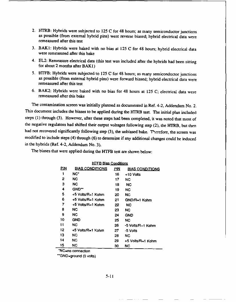
2. HTRB: Hybrids were subjected to 125 C for 48 hours; as many semiconductor junctionsas possible (from external hybrid pins) were reverse biased; hybrid electrical data wereremeasured after this test
3. BAKI: Hybrids were baked with no bias at 125 C for 48 hours; hybrid electrical datawere remeasured after this bake
4. EL2: Remeasure electrical data (this test was included after the hybrids had been sittingfor about 2 months after BAK1)
5. HTFB: Hybrids were subjected to 125 C for 48 hours; as many semiconductor junctionsas possible (from external hybrid pins) were forward biased; hybrid electrical data wereremeasured after this test
6. BAK2: Hybrids were baked with no bias for 48 hours at 125 C; electrical data wereremeasured after this bake
The contamination screen was initially planned as documented in Ref. 4-2, Addendum No. 2.This document includes the biases to be applied during the HTRB test. The initial plan includedsteps (1) through (3). However, after these steps had been completed, it was noted that most ofthe negative regulators had shifted their output voltages following step (2), the HTRB, but thenhad not recovered significantly following step (3), the unbiased bake. Therefore, the screen wasmodified to include steps (4) through (6) to determine if any additional changes could be inducedin the hybrids (Ref. 4-2, Addendum No. 3).
The biases that were applied during the HTFB test are shown below:
HTFB Bias ConditionsPIM BIAS CONDITIONS PIN BIAS CONDITIONS1 NC* 16 +10 Volts2 NC 17 NC3 NC 18 NC4 GND** 19 NC5 +5 Volts/R=l Kohm 20 NC6 +5 Volts/R=1 Kohm 21 GND/R=1 Kohm7 +5 Volts/R=1 Kohm 22 NC8 NC 23 NC9 NC 24 GND
10 GND 25 NC11 NC 26 -5 Volts/R=1 Kohm12 +5 Volts/R=1 Kohm 27 -5 Volts13 NC 28 NC14 NC 29 +5 Volts/R=1 Kohm15 NC 30 NC
*NC=no connection*'GND=ground (0 volts)
5-Il

Notes:
1. If no resistor is indicated after a bias, connection should bemade directly to the bias with no series resistor. If aresistor is indicated after a bias, that value of resistorshould be inserted between the bias and the pin.
2. These conditions are for hybrid P/N 934266 (the positivevoltage regulator). For Hybrid P/N 934268 (the negativevoltage regulator), negative voltages of the samemagnitude should be substituted for positive voltages, andpositive voltages for negative voltages.
At each point where electrical measurements are indicated the following data were measured
and recorded:
1. Overall hybrid functional parameters including regulated output voltage
2. Leakage currents across semiconductor junctions electrically accessible from externalhybrid pins
3. Resistance values of any resistors electrically accessible from external hybrid pins.
The leakage currents were monitored as an indication of overall hybrid cleanliness as
indicated by changes in the currents. The resistance values were monitored to assess the extent
to which the resistor failure mechanism seen in previous hybrid failures might be present. The
details of the leakage current and resistance measurements are documented in Ref. 4-2,
Addendum No. 2.
5.4.3 Results of Application of Screen to New HybridsThe 10 negative and 6 positive new regulator hybrids were subjected to the screen. The raw
data taken at each step in the hybrid screen are presented in Appendix Q. The leakage current
and resistance measurements did not reveal any significant information for either type of hybrid.
The negative regulator hybrids had slightly more instability in the resistance measurements, but
not enough to be significant.
The most significant result of the hybrid screen was the change in output voltages of the
negative voltage regulators. The values of the output voltage for the negative regulators for each
step in the hybrid screen are plotted in Figure 5-6. After the HTRB test, the hybrid output
voltages all increased for all devices except S/N 0480, assembled at a different time than the rest
of the devices and also a significantly different S/N.
The greatest change was in S/N 8584 which is shown on every graph so that it can be
compared to all other devices. Also, note that the output voltages tended to stay at the high
output levels all through the rest of the tests, decreasing only slightly for those showing the
biggest increase after the HTRB test.
5-12

1230
WL 12.18 ......... ..
1212 ............ / ..........tZ-------
0
12 ..............................................................................................
11.94INEL HTRB BAKI EL2 HTFB BAK2 BAK3
STEP
3 08584 *08872
008290 X 08589
12.30
IJH
0
0
11.94INEL HTRB BAKI EL2 HTFB BAK2 BAK3
STEP* 08584 (REPEAT) + 083880 08929 X< 07941
1230.
12 4 ............. ........w......... ...............................
CU... ................
12 8...................................
0
11 94IN~EL HTRB BAKI EL2 HTFB BAK2 BAK3
STEP* 08584 (REPEAT) + 083550 08784 >X 0480
Figure 5-6. Graphs of Output voltage at Each Step in the Hybrid ContaminationScreen for Negative Regulators.
5-13
Additional intervals of HTRB were performed on the negative regulators, but their outputs
never increased beyond the highest outputs observed in the HTRB performed in the screen test.
This indicates that the devices have degraded to the maximum extent possible with the amount of
ionic contamination present in the devices.
The output voltages of the positive voltage regulators were extremely stable all through the
series of tests. Figure 5-7 shows the behavior of the positive regulators. Figure 5-8 shows
expanded scales of the change in the output voltages of the positive regulators. Even on the
expanded scale no significant trend is noted for the positive regulators outputs.The screen, therefore, indicated that the ionic contamination failure mechanism is present in
the new negative regulators. However, the new hybrids apparently had less contamination than
the hybrids from the field as indicated by the smaller increase in output voltages. No indication
of the resistor failure mechanism was distinctly noted in the new hybrids. The new positive
regulators showed no indication of any of the failure mechanisms.
5.5 ANALYSIS OF NEW HYBRID
The negative regulator with the largest output voltage shift (S/N 8584) was analyzed to
determine the cause of the output change. Nodes in the hybrid were probed to determine the
voltage at each point. As in previous analyses of the negative regulators, the probing indicated
that transistors Q1 and Q2 were causing the output voltage shift.
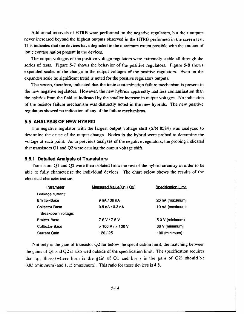
5.5.1 Detailed Analysis of Transistors
Transistors Q l and Q2 were then isolated from the rest of the hybrid circuitry in order to be
able to fully characterize the individual devices. The chart below shows the results of the
electrical characterization.
Parameter Measured Value(Q1 / Q2) Specifia i
Leakage current:
Emitter-Base 9 nA / 36 nA 20 nA (maximum)Collector-Base 0.5 nA / 0.3 nA 10 nA (maximum)
Breakdown voltage:
Emitter-Base 7.6 V / 7.6 V 5.0 V (minimum)
Collector-Base > 100 V I> 100 V 60 V (minimum)
Current Gain 120 / 25 100 (minimum)
Not only is the gain of transistor Q2 far below the specification limit, the matching between
the gains of Qi and Q2 is also well outside of the specification limit. The specification requires
that hFEj/hFE2 (where hFE1 is the gain of QI and hFE2 is the gain of Q2) should be
0.85 (minimum) and 1.15 (maximum). This ratio for these devices is 4.8.
5-14

POSITIVE REGULATORS12.30
0
0 & __& ______A,-_ it
11t94INEL HTRB BAKi EL2 HTFB BAK2
STEP0 11789 *12183
o 11650
POSITIVE REGULATORS
12 30
S 12 18 ........................... ............................. I......... . .............. I.... ...........0
0-
0l 1212 ................................. .............................................................
I- 1
12 ................................... .........................................................
11.94 0NEL HTRB BAKi EL2 HTFB BAK2
STEP
M 11861 0 12034 * 11836
Figure 5-7. Graph of Output Voltage at Each Step in the Hybrid ContaminationScreen for Positive Regulators. (Graph Axes Chosen to be Same
as for negative regulators (Figure 5-6) for direct comparison.)
5-15

POSITIVE REGULATORS (EXPANDED SCALE)45
40
I-
> 35...............
S 30 .................... ................... .............. ........................
cj /.
E
20 .. .- i--. ...................... ..
15
INEL HTRB BAK1 EL2 HTFB BAK2
STEP
* 11789 C1 11 o * 12183
POSITIVE HEGULATORS (EXPANDED SCALE)45
40 ........................... J ...................................................
w 30 ...... .... . ... .. .................... ................
0
20 . . ....... .......
151INEL HTRB BAKi EL-2 HTFB BAK2
STEP
U 11861 0 12034 % 11836
Figure 5-8. Plot of Data Shown in Figure 5-7 on an Expanded Scale.A Baseline Value of 12.0 Volts has been Subtracted
from Each Output Voltage in Figure 5-7.
5-16

The large difference in the gains of the two transistors is not explained by the small
difference in the leakage currents in the base-emitter junctions of the two devices. For such alarge difference in gains, several orders of magnitude of difference in the leakage currents would
be expected. Also, it should be noted that no evidence of a channel was noted in transistor Q2during curve tracer measurements of its electrical characteristics.
The hybrid, negative regulator SIN 8584, was reconfigured and the transistors rebonded so
that transistor parameters could be measured directly from the hybrid pins rather than having toprobe to the devices every time they needed to be characterized.
In order to further evaluate the base-emitter junctions of the two devices, the ideality factor,n, was measured for device base-emitter junctions. The ideality factor appears in the diode
equation:
I=Is exp( qVf/nKT)
where:
I = junction currenti s = saturation current (constant for a given device)
q = electron chargeVf = voltage across junction
K = Boltzmann's constantT = temperature
The value of n for a good junction varies between 1 and 2. For junctions affected by achannel the value lies between 3 and 4 (Refs. 5-1 and 5-2). In order to measure the value of n,the log of the current (I) is plotted versus the voltage (Vf) and the slope is measured. The value
of n can then be calculated from the slope.The values of n for Q1 and Q2 were measured using an automated setup that automatically
applies the voltage, measures the current and calculates the value of n for various ranges of Vf.
Figures 5-9 and 5-10 show the electrical data plots generated by the automated test equipment
and the values of n that were calculated for Q1 and Q2. While there were differences in thevalues of n for device base-emitter junctions, all values were in the range of 1 to 2, verifying thatthere is no channel associated with either device. It can also be seen that for equivalent forward
biases, transistor Ql conducts considerably less current than Q2. This information is presented
below:
Junction Current
JunctionVoltage 01 02(VBE)
0.12 V 10 pA 600 pA0.20 V 100 pA 40 nA0.30 V 1.05 nA 4n0 nA0.40 V 10.05 nA 3.0 uA
5-17

1E -2 ,
1E-3 VBE RANGE I CALCULATED Hn" _l
FROM 0. 10-O 07VL
1E -54 jf FROM 0.107 TO 0.207 VOLT 1.26II II
1E-5 -- I FROM 0207 TO00.307 VOLT 1 55 --
II III
1E I- FROM 0.307 TO 0.398 VOLT 160ii
<1E-*7W
1 E --
1E -1o ___ _ _ _ _ _ _
lE -
r
0100 0.200 0300 0.400VBE-(VOLTS)
Figure 5-9. Plot Of 'BE vs. VBE for Transistor Q1. The Computed Values of theIdeality Factor, n, are Shown for Various Ranges Of VBE.
1E-0 _-2_ -- _
1E 3 B RANGE CALCULATED "n"
E 3 -- -'
1E -4 FROM 107T00 0.207 VOLT 4166
1E -5 FROMO0 207 T 0 V307 VOLT 1 77
II { II I
1 E 46 FROM 0 307 TO 0.398 VOLT I 190
1E -47 _1 ___1.66
wT 1E-8I
1E 5----lFO 0 O0 0 OT917 -
1E 10
1E -11-
1 E -1 24--- + - -
0 100 0200 0300 0400VBE (VOLTS)
Figure 5-10. Plot Of 11BE vs. VBE for Transistor 02. The Computed Values of theIdeality Factor, n, are Shown for Various Ranges Of VBE.
5-18

The cause for the higher currents in Q2 is discussed in detail in Section 5.7.3. These higher
currents are directly related to the decreased current gain of Q2.
The ideality factor was also measured for the collector-base junctions. The individual
behavior of this junction would have less of an influence (than the base-emitter junction) on the
overall behavior of the transistor, especially on the transistor gain. The ideality factor wasmeasured as another indication of the electrical behavior of one transistor relative to the other.
Since these devices started out as a matched pair, this measurement provided more information
on their present conditions.
For the base-collector junctions of Q1 and Q2, the currents for the two junctions were
virtually identical except at very low forward bias voltage. The ideality factors were also verysimilar, again being different only at very low forward bias voltages. The differences at very lowbias would not affect the behavior of the transistors at normal biases.
5.5.2 Additional Tests on TransistorsThe devices were then subjected to an unbiased bake and then a period of HTRB (high
temperature reverse bias). The unbiased bake was performed at 100 C for 96 hours in a nitrogen
atmosphere. The HTRB was performed for 48 hours at 125 C with 5-V reverse bias on the base-
emitter junction and 10 V reverse bias on the base-collector junction.
The devices were electrically characterized both after the unbiased bake and after the HTRB
stress. The electrical parameters, including the ideality factor, did not change significantly after
either test for either of the transistors.
The devices were examined in the SEM (scanning electron microscope) and analyzed to
cetermine if there was any detectable contamination on the device. EDX (energy dispersive
X-ray) analysis of the surface of the transistors did not reveal the presence of any contaminants.
However, EDX analysis requires that an element be present in concentrations of at least
0.1% to be detectable. There could be more than enough sodium present in the oxide on the
devices to cause changes in their electrical behavior.
When sodium causes inversion in an integrated circuit, the concentration levels are on theorder of 10 times the concentration of the dopants in the silicon. The dopant levels in the silicon
are only on the order of 0.1 ppm to 10 ppm. Therefore, sodium concentrations of I ppm to 100ppm are sufficient to cause problems. These levels will not be detected by EDX analysis.
5.6 COMPUTER MODEL OF HYBRID CIRCUITPrevious analyses have indicated that change in gain of one of the transistors in the matchedtransistor pair caused the voltage output of the negative voltage regulator hybrid to change. In
order to investigate the relationship between mismatch in the gains of the previously matched
5-19

transistors and the output voltage of the hybrid, it was decided to use a computer model of the
hybrid circuit to simulate the behavior of the hybrid. Using this approach, different gains for
each of the transistors in the matched pair were input into the computer model and then the
computer model was used to determine the resulting hybrid output voltage.
5.6.1 Advantages of Computer Simulation
It would have been virtually impossible to find actual transistor chips with the correct range
of gains to physically replace the transistors in the hybrid and then monitor the resulting output
voltages. Also, the effort required for such an approach would have been considerable. The
potential for erroneous results as the result of either mechanical damage to other components in
the hybrid or contamination introduced during this type of approach would also have tended to
make this type of approach unfeasible.
The only other approach that could have been attempted using actual hardware would have
been to alter the function of the circuit using electrical microprobes. By probing to the interior of
the hybrid and placing a resistor across the base-emitter junction of each of the transistors in the
matched transistor pair, a parasitic leakage current could have been created to effectively reduce
the gain of one or both of the transistors. This would still require calculation of the effective gain
of the transistor in the circuit and would not be completely equivalent to actually having a
transistor in the circuit with reduced gain. Again this approach would have had the possibility of
erroneous results due to mechanical damage to other components in the hybrids or the possibility
of the potential for contamination introduced into the hybrid.
5.6.2 Generation of Computer Model
The hybrid by itself is not a functional voltage regulator. Obviously external power supplies
and input voltages have to be connected to the appropriate hybrid pins. Also, other connections
ano components must be applied to the hybrid depending or. the desired output voltage. The
hybrid is capable of supplying various regulated negative voltages (-5, -6, -12, -25 or -50 volts)
depending on the input voltage applied and the various external connections. Details of the
connection requirements for each voltage can be found in the Hughes Standard 934268 shown in
Appendix 0.
The software that was used for the circuit simulation was Microcap which is a version of
SPICE. The circuit simulation included the circuitry in the hybrid plus the external circuitry and
power supplies required to generate a complete voltage regulator. Initially, the circuit simulation
was performed with the hybrid configured as a -5-volt regulator.
The computer model was generated by choosing a point in the circuit that was modelled and
then specifying a component or components to be connected to this point. The components were
5-20

then specified that were to be connected to the other terminals of the previously selected
components until the entire schematic was generated. Initially, the components were only
denoted by their type and circuit number. For example, RI for resistor number 1, C3 for
capacitor number 3 and so forth. After the circuit diagram was completed, a list of ,he
components was generated by the computer and specific values were assigned to the resistors and
capacitors.
Models for various transistors and diodes have already been included in the software.
Common models were chosen for each of the transistors in the hybrid circuit. Of course, care
was taken to ensure that PNP models were used for PNP transistors and NPN models for NPN
transistors. Simple diode models were chosen for the diodes, except in the case of the Zeners
where models were chosen corresponding to the correct Zener voltage. Transistors Q I and Q2
were modelled using the common PNP transistor model that was included in the software, except
the gain was modified so that initially both transistors had equivalent gains of 120.
5.6.3 Testing the Model
The first runs of the model revealed that it took a long time (about 20 minutes) for the model
to converge to a steady state solution. However, when the model did converge the hybrid circuit
output voltage was very close to the specified output. The model output was -5.0002 volts when
the specified output should be -5.00 volts ±0.5% (or ±025 volts).
On subsequent runs, it was discovered that the Zeners were causing the long convergence
time. By replacing one or both Zeners with a power supply equivalent in voltage to the Zener
voltage, the model would converge to a solution within 1 or 2 minutes. It was hypothesized that
the software was having a problem with both Zeners in the circuit at the same time. Since the
Zener I-V characteristic has such an abrupt discontinuity (the Zener current is zero until the
Zener voltage is reached), the software seemed to be having a problem at startup, trying to reach
the point where both Zeners are conducting simultaneously. However, using the power supply in
place of one or both devices forces the circuit simulation to converge much more rapidly.
Using the power supply in place of one Zener caused a small shift in output voltage and
replacing both Zeners with supplies resulted in a slightly higher shift. For example, with both
Zeners replaced by power supplies, the output of the circuit was -5.026 volts. With the 6.2 V
Zener replaced by a supply, the output was -5.020 volts and with the 4 V Zener replaced it was
-5.024 volts. By trimming one of the resistors in the circuit, the offset introduced by using a
supply in place of a Zener could be zeroed out without affecting the overall performance of the
circuit. Most of the simulations were run with one of the Zeners replaced by a power supply in
the computer model in order to speed up the convergence time. Whenever a significant change
5-21
was made in the hybrid circuit, an occasional trial run was made with both Zeners in place to
confirm that the power supply was not significantly altering the hybrid circuit behavior.
5.6.4 Modelling the Regulator with Mismatched Transistors
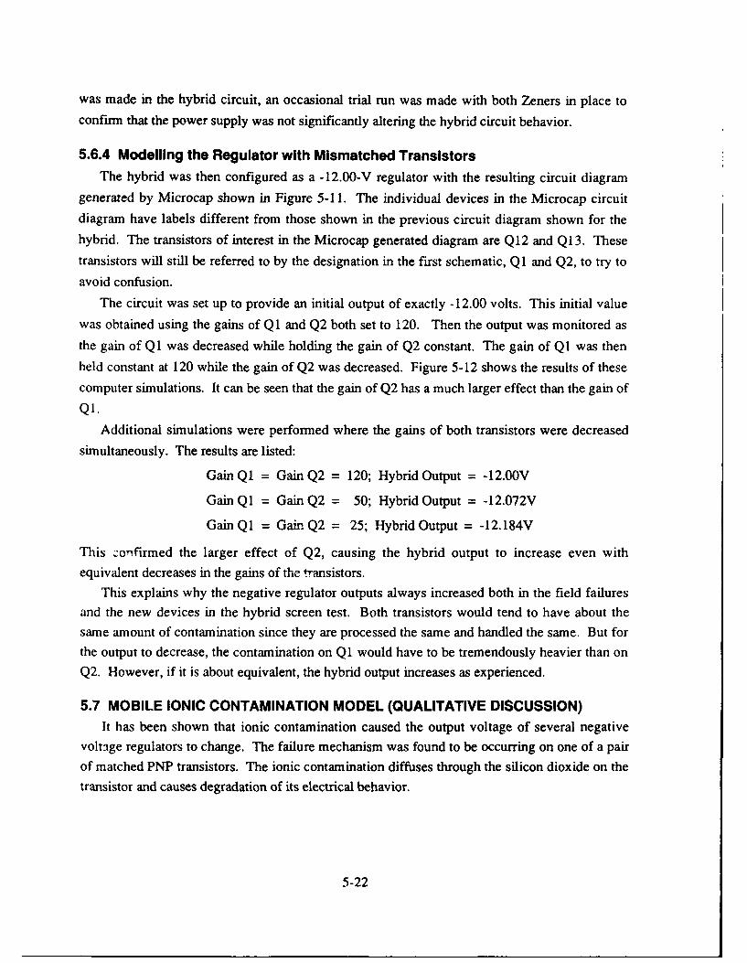
The hybrid was then configured as a -12.00-V regulator with the resulting circuit diagram
generated by Microcap shown in Figure 5-11. The individual devices in the Microcap circuit
diagram have labels different from those shown in the previous circuit diagram shown for thehybrid. The transistors of interest in the Microcap generated diagram are Q12 and Q13. These
transistors will still be referred to by the designation in the first schematic, QI and Q2, to try to
avoid confusion.
The circuit was set up to provide an initial output of exactly -12.00 volts. This initial value
was obtained using the gains of Q1 and Q2 both set to 120. Then the output was monitored as
the gain of Q1 was decreased while holding the gain of Q2 constant. The gain of Q1 was then
held constant at 120 while the gain of Q2 was decreased. Figure 5-12 shows the results of these
computer simulations. It can be seen that the gain of Q2 has a much larger effect than the gain of
Ql.Additional simulations were performed where the gains of both transistors were decreased
simultaneously. The results are listed:
Gain QI = Gain Q2 = 120; Hybrid Output = -12.OOV
Gain QI = Gain Q2 = 50; Hybrid Output = -12.072V
Gain Qi = Gain Q2 = 25; Hybrid Output = -12.184V
This zo-ifirmed the larger effect of Q2, causing the hybrid output to increase even with
equivalent decreases in the gains of the transistors.
This explains why the negative regulator outputs always increased both in the field failuresand the new devices in the hybrid screen test. Both transistors would tend to have about thesame amount of contamination since they are processed the same and handled the same. But forthe output to decrease, the contamination on Q1 would have to be tremendously heavier than on
Q2. However, if it is about equivalent, the hybrid output increases as experienced.
5.7 MOBILE IONIC CONTAMINATION MODEL (QUALITATIVE DISCUSSION)It has been shown that ionic contamination caused the output voltage of several negative
voltage regulators to change. The failure mechanism was found to be occurring on one of a pairof matched PNP transistors. The ionic contamination diffuses through the silicon dioxide on the
transistor and causes degradation of its electrical behavior.
5-22

V(1)VIN
VI 17V R4.2 IVi R 7 0N2907 a
RI~ 03QN2 22 1 ~ R768~ 150 3.32K
281 J 1 1 L 1V(11)DI BDN4002 R5.1 B
15V(15) V3 17V V(21)R2606 E 23 + D( 1 / D6R2317 ON2222 " 2/V(25) R16 23-, "
R19 ZN4V
F: R15 <.93300PF 16 365 18 K 1K ( 15)
L -A -6 V(21) 21 22V ) E
010 17 RIO D _ /2 -D3 V(9)ON2907 1.6K DN4002 VOUT217
V(1 7) 594 N4002 2 ) 26 R 0 2
• V 7 94 N4002 T DN40020 / 14 - R20 5R2205 N2222 CV4
F1 t
R3 .QS 0N 2 1 , C V _!(12 | 30 50 333_V(33) 3 .4 5 1 K
R V(36) 6.2V R12
200 A + J 600 0 VOUTIW13 10 24 R21
1-25K 2I I.K11 V( 7) C100PF
V(36) A 013
R23 O N120
04 { V(22)D4 z
DN4002 Z
V(i1) B
Figure 5-1 1. Negative Voltage Regulator Circuit Diagram Generated by Circuit Simulation Software.Includes Hybrid Circuitry Plus External Circuitry and Connections Required for aComplete Regulator. Component Labels Differ from Those in Figure 5-3. 012 and013 Correspond to 01 and 02 in Figure 5-3. (6.2 V Zener Diode Replaced by 6.2 VPower Supply.)
5-23

6
5
GAIN 01 120
GAIN 02
4
OUTPUT VOLTAGEDEVIATION (%)
(NEGATIVE FOR 3GAIN 02> 01,POSITIVE FORGAIN 0 1 > 0 2)
2
00
1 2 4 6 8 10 12
TRANSISTOR GAIN RATIO
Figure 5-12. Plot of Negative Regulator Output Deviation (in %) vs. Ratio of Gains ofTransistors Q1 and 02. "+" Data Points are for the Condition where Gain of 01was Held Constant and Gain of Q2 was Varied. "o" Data Points are for theCondition where Gain of 02 was Held Constant and Gain of Q1 was Varied.Data for Plots was Generated by Computer Circuit Simulation.
5-24

A model was generated to simulate the diffusion of the ionic contamination through the oxideover the semiconductor. The model also determined the resulting amount of charge that wasinduced in the silicon beneath the oxide and the resulting effects on the electrical behavior of the
transistor.
Ultimately, the model was used to predict the lifetimes of the hybrids under known operatingconditions. These hybrids were to be installed in units identical to the units in which the fieldfailures were installed. These units were then placed in a CERT (Combined EnvironmentsReliability Test) for a certain period of time (see Section 6.0). The CERT subjected the units toconditions that were more extreme than those that they would see in the field. Since theconditions for the CERT were carefully controlled, the stress factors could be input into themodels to predict the amount of time the hybrids would operate before they failed. The failure
criteria were the module specification limits for the negative regulator hybrid output voltage.
5.7.1 Detailed Transistor DescriptionIt has been shown that the gain of the PNP transistors in the hybrids has been degraded by
ionic contamination, probably in the form of sodium ions, that diffused through the passivationoxide. An initial description of the transistors was given in Section 5.3.1. This present sectionprovides additional details needed to understand the failure mechanism that occurred in these
devices.
Figure 5-5 shows a photograph of one of the PNP transistors. Figure 5-13 is a sketch of a
cross section of the transistor showing how the different diffusions are located to form the p-type
emitter, n-type base and p-type collector regions. The portion of the transistor that is affected bythe ionic contamination is the surface of the device near the base-emitter junction. Figure 5-14 is
a sketch of this area in a location where metallization passes over the base-emitter junction.
COLLECTOR
SHADED AREA = EMITTER
Figure 5-13. Sketch of Q2 Cross Section Showing Positionsof Base and Emitter Diffusions Relative to Collector.
5-25

When the transistor was fabricated, the n-type base diffusion was diffused into the p-type
collector. In order for the base to be n-type it must have a much higher doping level than the
collector diffusion into which it was diffused. The n-type dopants for the base are diffused into a
portion of the collector which already contains p-type dopants. The n-type and p-type dopants
tend to cancel each other at the point where the concentrations of the two dopant types are
equivalent. Additional n-type dopants are added until the concentration of the n- type dopants in
the base area are at least 1.5 to 2.0 orders of magnitude greater than the dopant concentration of
the p-type dopants already present due to the collector doping. At this point the effects of the
p-type dopants are completely overcome and the material behaves electrically as if it were n-type
material.
The preceding discussion also applies to the formation of the emitter diffusion, except in this
case, the p-type emitter diffusion was formed in the n-type base diffusion. As a result, the p-type
emitter diffusion doping concentration is at least 1.5 to 2.0 times greater than that of the base.
The doping concentration of the emitter will be very high as a result.
The doping concentration of the base diffusion can be approximated by measuring the
breakdown voltage of the base-emitter junction. The breakdown voltage of the base-emitter
junction was about 7.6 volts for three different samples of the transistor of interest. This
corresponds to a doping level of approximately 2.5 x 10¹⁷ atoms/cc (Ref. 5-3). The emitter
doping concentration will therefore be approximately 1019 atoms/cc.
5.7.2 Ionic (Sodium) Contamination DiffusionWhen sodium ionic contamination is discussed in the technical literature, most references
agree that the sodium contamination is probably introduced as an artifact during the aluminum
metallization deposition process. Therefore, when it is initially introduced it can be assumed that
it exists as a layer between the aluminum and the silicon dioxide passivation as indicated in
Figure 5-15. There may also be some immobile sodium in the metallization and also some
sodium on top of the metallization. These will be neglected for the purposes of this model.
Sodium will diffuse through silicon dioxide at a rate that is very temperature dependent.
(Sodium will also diffuse through silicon nitride, an alternate passivation material, but at a rateapproximately an order of magnitude slower than through silicon dioxide.) Therefore, as time
goes by the sodium will diffuse into the oxide generating a distribution that can be represented as
shown in Figure 5-16. The positive sodium ions will attract negative carriers in the underlying
silicon. In the case of the n-type base, the additional negative carriers that are attracted to the
surface will make this region more heavily doped n-type, an effect known as accumulation. Inthe case of the p-type emitter, the negative carriers (minority carriers in this region) that are
attracted by the sodium ions will tend to make the surface region less p-type. If enough negative
5-26

METALLIZATION
OXIDE
SILICON N-TYPE P-TYPEBASE EMITTER
Figure 5-14. Sketch of Cross Section of Surface ofTransistor Over the Base-Emitter Junction.
carriers are attracted by the ionic contamination, the surface of the p-type emitter will have more
negative carriers than positive carriers and will become inverted to n-type material. The area
where it becomes inverted is known as the inversion layer.
In most cases where ionic contamination in the passivating oxide is affecting the electrical
behavior of a device, the contamination has inverted the silicon directly beneath the oxide. In the
case of sodium or positive ionic contamination, only p-type material can be inverted. For the
PNP transistor of interest, only the collector or emitter diffusions can be affected by sodium
contamination. From previous discussions of the electrical behavior of the device, the emitter
diffusion is the area that is being affected by the contaminant. At first, this does not seem
possible since the emitter diffusion is so heavily dopCcd
Typically, heavily doped areas are immur, to being inverted since the concentration of the
contaminant is no sufficient to induce enough charge in the silicon to overcome the doping in
the silicon. However, for heavily doped junctions, contamination in the oxide can lead to a
different type of degradation mechanism.
5.7.3 Tunneling - Failure MechanismDuring a literature search for data on the quantitative effects of ionic contamination on device
electrical characteristics, a discussion of degraded gain in PNP transistors and a description of
the failure mechanism were tound. (Numerous other references regarding ionic contamination,
sodium diffusion in oyides and the effects on semiconductor performance were reviewed. These
are listed at the end of the cited references for Section 5.0.) The failure mechanism is tunneling
in the base-emitter junction induced by ionic contamination in the overlying oxide (Ref. 5-2 and
5-4). The base-emitter tunneling current does not contribute to the gain of the device but does
5-27

increase the overall base current. Therefore, the gain or hFE which is simply IC'IB (where IC is
the collector current and IB is the base current) decreases since the collector current stays
constant while the base current increases.
The failure mechanism results when the ionic contamination (sodium) inverts a portion of the
p-type emitter area. Figure 5-17 represents the doping concentrations across the surface of the
base-emitter junction of the transistor that was degraded by ionic contamination in the negative
regulator hybrids. The n-type concentration is about 2.5 x 10¹⁷ atoms / cc in the base and
becomes p-type at a concentration of about 1019 atoms / cc in the emitter. The transition
between the two areas is depicted as a linear change (on a log scale) between these two regions.
Tl- actual transition is not important. This representation was chosen only for the purposes of
the following discussion which will not be extremely dependent on the exact shape of the
transition between the two regions.
Along the area of transition between the base and emitter regions, there are p-type doping
levels that range from zero to 1019 atoms / cc. Some of these p-type levels will be subject to
being inverted by ionic contamination in the overlying passivating oxide. As a result, n-type
regions can be formed in the area that was formerly the transition region, resulting in very
closely located highly doped p-type (represented by p+) and n-type regioais. This geometry is
susceptible to tunneling conduction between the two regions as opposed to the normal
conduction mechanisms.
Figure 5-18 shows an energy band diagram for a p-n junction. For the n-type region, the
Fermi level in the material is located nearer to the conduction band than to the valence band due
to the excess number of electrons in this area. In the p-type region, the Fermi level is located
nearer to the valence band due to a lack of electrons (or the presence of holes) in this area. When
the p- and n-type materials are adjacent, the Fermi levels from the two materials align resulting
in a potential difference between the p- and n-type regions. This potential difference is
responsible for the rectifying properties of a p-n junction.
When the junction is forward biased (as illustrated in Figure 5-19), the potential difference
between the p and n regions is reduced. With sufficient bias applied, the potential difference is
reduced sufficien tly such that current flows across the junction. With the opposite polarity
applied, the junction is reverse biased and the potential difference between the two regions
increases and further blocks current flow.
5-28

METALLIZATION
OXIDE M
SILICON
Figure 5-15. Sketch of Cross Section of Surface ofTransistor Showing Initial Thin Layer of Sodium
Introduced During Metallization Deposition.
METALLIZATION
OXIDE K- P(x)
SILICON QSI
Figure 5-16. Sketch of Cross Section of Surface of Transistor AfterSodium has Diffused into the Oxide. The "x" Coordinateis Distance into the Oxide from the Metallization/OxideInterface. p(x) is the Amount of Sodium at Each Layer ofOxide at Distance x into the Oxide. The SodiumDistribution Induces a Charge in the Surface of the SiliconRepresented by QSI. TOX is the Oxide Thickness.
5-29

P
- 1019-
~ 1018 P+ TYPE
N TYPE 2.5x 10¹⁷
BASE EMITTER
N
Figure 5-17. Representation of Doping Levels Across Base-Emitter Junction.Base is N-type and Emitter is P-type with Transition in Between.
5-30

N TYPE /
CONDUCTION
I ERP LE VELBAND GAP P TYPE
VALENCE
UNBIASED
Figure 5-18. Diagram of Energy Levels in a Typical P-NJunction (Without Bias).
N TYPE
VF
SP TYPE
FORWARD BIASED
Figure 5-19. Diagram of Energy Levels in a Typical P-N Junctionwith Forward Bias. Energy Level Difference Between
p- and n-Type Regions is Reduced by VF,the Forward Bias Voltage.
5-31
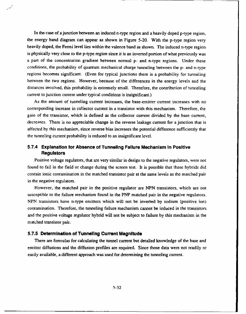
In the case of a junction between an induced n-type region and a heavily doped p-type region,
the energy band diagram can appear as shown in Figure 5-20. With the p-type region very
heavily doped, the Fermi level lies within the valence band as shown. The induced n-type region
is physically very close to the p-type region since it is an inverted portion of what previously was
a part of the concentration gradient between normal p- and n-type regions. Under these
conditions, the probability of quantum mechanical charge tunneling between the p- and n-type
regions becomes significant. (Even for typical junctions there is a probability for tunneling
between the two regions. However, because of the differences in the energy levels and the
distances involved, this probability is extremely small. Therefore, the contribution of tunneling
current to junction current under typical conditions is insignificant.)
As the amount of tunneling current increases, the base-emitter current increases with no
corresponding increase in collector current in a transistor with this mechanism. Therefore, the
gain of the transistor, which is defined as the collector current divided by the base current,
decreases. There is no appreciable change in the reverse leakage current for a junction that is
affected by this mechanism, since reverse bias increases the potential difference sufficiently that
the tunneling current probability is reduced to an insignificant level.
5.7.4 Explanation for Absence of Tunneling Failure Mechanism In PositiveRegulators
Positive voltage regulators, that are very similar in design to the negative regulators, were not
found to fail in the field or change during the screen test. It is possible that these hybrids did
contain ionic contamination in the matched transistor pair at the same levels as the matched pair
in the negative regulators.
However, the matched pair in the positive regulator are NPN transistors, which are not
susceptible to the failure mechanism found in the PNP matched pair in the negative regulators.
NPN transistors have n-type emitters which will not be inverted by sodium (positive ion)
contamination. Therefore, the tunneling failure mechanism cannot be induced in the transistors
and the positive voltage regulator hybrid will not be subject to failure by this mechanism in the
matched transistor pair.
5.7.5 Determination of Tunneling Current MagnitudeThere are formulas for calculating the tunnel current but detailed knowledge of the base and
emitter diffusions and the diffusion profiles are required. Since those data were not readily or
easily available, a different approach was used for determining the tunneling current.
5-32

N (DUE TO INVERSION) TUNNEL CURRENT
P+ EMITTER
Figure 5-20. In a p-n Junction with Heavy Doping (in this Case the p-Type Material is HeavilyDoped) the Fermi Level (Dotted Line) Can Ue Within the Valence Band. The n-TypeRegion, Formed by Inversion of a Portion of p-Region, is Very Close to the p + Region.In this Situation, the Quantum Mechanical Tunneling Probability Becomes Significant.
5-33

Ref. 5-4 is a summary of experiments on various transistor structures using an additional
metallization as a gate structure to determine the effects of various contaminants on transistorparameters. The metallization was deposited over the passivating oxide above the base-emitter
junction on the different transistors. Varying biases were then applied to this metallization.
Since the thickness of the oxide over the base-emitter metallization was known the resulting field
induced by the bias on the metallization could be determined. This induced field could then be
used to simulate the fields induced by varying levels of contamination that might be in the oxide.Since the polarity on the gate metallization could be either positive or negative, the effects of
either positive or negative ions could be simulated.
When the metallization was positively biased over the base-emitter of a PNP transistor, the
gain of the transistor was found to decrease. This is analogous to the gain degradation that was
observed on the transistors of interest from the hybrids. The article went on to explain that thiswas due to base-emitter tunneling current resulting from changes in the base-emitter junction
induced by the field in the oxide. Other references also discuss this phenomena but do not
provide as much detailed quantitative data as this reference.
Using the data from this reference, the tunneling current density vs. surface charge per unit
area was calculated for the test structure. The transistor biases and nominal operating currentswere also included in the data in the reference and can be chosen so that they are the same as the
operating conditions for the actual transistors in the hybrid. The doping profiles for the test
transistors in the reference and the actual transistor in the hybrid do not have to be known or have
to be exactly the same since the failure mechanism occurs along the concentration gradient
between the base and the emitter diffusions rather than at a particular concentration value. Since
the diffusions in both transistors were created in similar manners, the concentration gradients
would be similar enough to predict the tunneling current for the transistor from the hybrid to well
within an order of magnitude, based on the data for the transistor in the reference.
Once the. tunneling current has been determined for the transistor, the change in gain for the
transistor can be determined. This gain change will then determine the output voltage change for
the overall hybrid.
5.7.6 Hybrid Output Voltage vs. Transistor Gain Degradation
The data for the computer simulation of the hybrid circuit were used to determine the
resulting output voltage for a particular value of gain for transistor Q2. The model for the ionic
contamination failure was ultimately used to predict the lifetime of the hybrid under particular
operating conditions. The criteria for failure was the module specification limits for the hybrid
output voltage. This voltage was then used to determine the amount of gain change required for
the hybrid to shift to this voltage.
5-34

5.8 MOBILE IONIC CONTAMINATION (QUANTITATIVE DISCUSSION)The preceding section discussed the general approach for the ionic contamination model.
This section provides a detailed discussion of the model with quantitative data produced by themodel. The model was coded in Tasks VII and VIII, and the software was delivered to the Air
Force.
5.8.1 Overall ApproachFigure 5-21 is a flow chart representing the overall model for the ionic contamination
mechanism. The sodium ion diffusion model predicted the diffusion profile of sodium ions inthe oxide of the transistor vs. time. Also, this model was used to calculate the resulting charge
vs. time induced in the underlying silicon. The charge induced in the silicon was then input intothe data from the reference on tunneling currents to predict the amount of tunneling currentwhich was then translated into change of gain vs. time. The maximum allowable change in gain
was obtained from the computer simulation of the hybrid circuit.ICIRCUIT
MODEL
,MAX AH-FE[ NA+ OsIlo ) TUNNELING A H'FEMt) MAXIMUM
DIFFUSION -" CURRENT AH'FEMODEL MODEL ALLOWABLE
Figure 5-21. Flow Chart for Ionic ContaminationInduced Inversion Model.
By observing the change in gain vs. time, the point at which the maximum allowable gainchange is reached can be determined. This point corresponds to the predicted time that thehybrid will operate without failure. This time is referred to as the FFOP (Failure Free Operating
Period) of the hybrid.
5.8.2 Sodium Ion Diffusion ModelReferring back to Figures 5-15 and 5-16, p(x) represents the distribution of sodium ions in
the oxide throughout its total thickness Tox. Each point, p(x), represents the charge in a layer of
oxide x distance away from the metallization. The function p(x) was calculated using standard
diffusion formulas.
5-35

For an initially limited source, that is, where the source of the diffusing element is finite
(Ref. 5-3):
C ( , t) =X 2
YcDt e(5-1)
where:
C(x,t) = concentration of element at point x at time t
S = initial surface concentration of diffusing element
D = diffusion coefficient of diffusing element.
There would be very little difficulty in programming this equation and providing the
distribution of sodium ions at any point in time. However, there are two complications that make
this problem much more difficult:
(1) The above equation is for an infinitely thick medium
(2) D is dependent on temperature !according to the following formula:
D = Do exp (-EA/KT) (5-2)
where:
Do = diffusion constant at known temperature
EA = activation energy
K = Boltzmann's constant
T = absolute temperature
These complications to the problem are solvable. The equations and model for solid
diffusion are similar to heat conduction problems that have already been solved. Basically, the
approach is to calculate distributions for a time and constant temperature interval and then use
this as the initial point for the next interval. The initial value of the sodium ion surface
concentration, S, was estimated to be on the order of I x 10 exp 14 atoms/cm 2 based on data
from the technical literature. Of course, the actual value for this specific transistor could be
orders of magnitude different from this "typical" value from the literature.Values of EA and D were also obtained from the literature (Refs.5-5 through 5-8). The value
used for EA was 1.4 eV and D was 2.16 x 10⁻¹⁶ cm2/sec at 125 C.
5-36

5.8.3 Charge Induced In the SiliconOnce a distribution of sodium ions has been determined for a particular time, the charge
induced on the underlying silicon can be calculated using the following formulas:
Q M = T0 x p (x) dxTOX (5-3)
= | Tox'X p()d
f Tox (5-4)
where:QM = charge induced on the metallization by the sodium
QSI = charge induced in the silicon by the sodium
Tox = total oxide thickness
The oxide thickness was initially estimated to be 1 micron. This value was later verified by
actually cross-sectioning one of the transistor chips and measuring the oxide thickness. The
measured thickness was 1.0 micron.
A computer model was developed for determining the charge induced in the silicon by a
sodium ion distribution at a particular time. The amount of surface charge was determined up to
a point where a "critical level" of surface charge was obtained. The "critical level" is defined as
the point where sufficient charge has accumulated to degrade transistor gain sufficiently that
hybrid output is outside of specification limits.
The initial calculations were simply an integration of the form
K I X exp (- X2 K2 ) (5-5)
If a critical level of surface charge had not been reached by the time some of the sodium ionshad reached the silicon surface (the finite thickness condition), then the sodium ion distributionwould have had to be numerically integrated. Numerical integration also has to be used if
distributions have to be calculated for time intervals at different temperatures.
Using the quantitative data from the previously mentioned reference, it was determined that asurface charge of about 7.5 x 10⁻¹² charges / cm 2 would correspond to the "critical level" of
surface charge. With this amount of surface charge induced in the transistor, the gain oftransistor Q2 would decrease to the point where hybrid output voltage would increase to the
maximum module specification limit of -12.25 volts.
5-37

Figure 5-22 shows the initial outputs of the computer model. The graph produced by thecomputer shows the charge induced in the silicon (QsI) normalized to the initial sodium ionconcentration (QNa+) vs. time for various temperatures. By normalizing the induced charge to
the initial sodium ion charge, assumptions regarding the amount of initial sodium charge wereneglected at this point. It can be seen that, at temperatures of 100 C or less, it will take thousandsof hours to reach an induced silicon charge equivalent to only 10% of the initial sodium charge.For a temperature of 125 C, this time is reduced to only about 80 hours. However, in theseexamples the transistor could further degrade to a much larger extent if subjected to additionaltemperature since the sodium ions have not reached an equilibrium distribution where QSI/QNa+
= 0.5.
If the sodium were allowed tc diffuse for an infinite amount of time, the final distributionwould be an even distribution of sodium throughout the thickness of the oxide. Under theseconditions, the charge induced in the silicon would be equivalent to one-half of the total numberof sodium ions that were initially introduced in the oxide. This amount of surface chargecorresponds to having all of the sodium ions distributed halfway between the metallization andthe silicon, at x = Tox/2.
However, the contamination screen that was applied to the hybrids resulted in large voltageshifts in the hybrids in only 48 hours (see Section 5.4). One hybrid output voltage even shiftedbeyond the specification limit allowed by the module specification.
Even more significant is the fact that the hybrids did not degrade any more when subjected toadditional high temperature testing. It was as if they had already reached an equilibriumdistribution of sodium ions after only 48 hours (or sooner, since no data were taken at anyintervals between the initial value and the first end point value at 48 hours).
The previous calculations and computer model assumed that the transistors were biased asthey normally are in the hybrid. That is, the base-emitter junction is forward biased with onlyabout 0.5 to 0.6 volt across the junction. However, in the HTRB step of the hybridcontamination screen, the base-emitter junction of the transistors is reverse biased with 5 voltsacross the junction. Since the base metallization crosses over the junction, there was a field of 5volts across this oxide. The HTRB base bias of +5 volts with respect to the emitter tended todrive the sodium ions away from this metallization toward the junction, especially toward theemitter. This field that resulted from the HTRB test apparently had a large effect on the sodium
ions.
5-38

05
04 Z 140 0C
03
OS'.
02
Ole
I01
/5' 25AN-5
TIME (HOURS)
si(CHARGE INDUCED IN SILICON) NORMALIZED TOO0 Na+ (INITIALSODIUM CONCENTRATION) VERSUS TIME FOR VARIOUSTEMPERATURES OXIDE THICKNESS (To,) IS I MICRON.
Figure 5-22. Output from Computer Model of Sodium Diffusion (for Normal Bias).
5-39

5.8.4 Modification of Model to Include Reverse BiasIt was decided to modify the computer model to include the field induced across the oxide by
the reverse bias. (The lateral field induced across the base-emitter junction was neglected tomake the geometry of the problem simpler.)
There were two approaches that were considered for including the reverse bias in themodel. The first was to directly solve Fick's second law modified to include the reverse bias.The following equation (Ref. 5-9) shows this modification:
-" = D x2- -- (5-6)
In this equation, we have (Refs. 5-3 and 5-10)
SREVERSE BIAS VOLTAGE)OXIDE T ICKNESS ) (5-7)
eD(5-8)
where:
v = velocity of the diffusing ions
p = mobility of the diffusing ions
L' = electric field across the oxide.
This approach would have been very difficult even using a computer model, especially whenthe effects of varying the temperature and the finite medium are taken into account.
The second approach that was evaluated, and ultimately used, was to use a mathematicaldevice to solve the problem. First, a mathematical substitution known as Smolukhovskii'ssubstitution (Ref. 5-10) was used:
Vx Vt
C = e -"- "hC* (5-9)
Then Fick's second law was solved based on this new variable:
aC * 02C *
7t- D 2 Cx (5-10)Ot x2
This was then modelled on the computer and new curves of sodium distribution vs. time were
calculated for 125 C.
5-4)
Figure 5-23 shows these curves for the reverse biased case and for the unbiased (or normal
bias) case. It can be seen that the reverse bias greatly accelerates the diffusion of the sodium
ions. The sodium ion distribution achieves an effect equivalent to an equilibrium distribution
(QsI = QNa+12 ) in only 34 hours under HTRB conditions. In comparison, Figure 5-22 shovis
that unbiased diffusion will require more than 1000 hours to have this sane effect.
The reverse bias curve explains another detail that was seen during the HTRB performed in
the hybrid contamination screen. For periods of HTRB greater than 34 hours, the sodium
contamination will be driven beyond an equilibrium distribution. That is, the "average position"
for the sodium ions will be closer to the silicon than that for the equilibrium condition.
The HTRB in the screen was performed for 48 hours. Examination of the data for the
negative regulators presented in Figure 5-6 shows that the devices with the largest output voltage
shifts did recover slightly when they were baked without reverse bias. This - uld be a result of
the sodium ions "back-diffusing" from th distribution resulting from the HTRB. As the
distribution approaches the equilibrium condition, the transistors recover slightly since the"average position" of the ions is now farther away from the silicon.
5.9 MODEL OF SURFACE CONTAMINATION MECHANISM
It has been shown that surface contamination caused the output voltage of some of the fielded
negative regulator hybrids built in 1981 and 1982 t, -hange. The failure mechanism was found
to be occurring on a thick film resistor. Apparently, the surface contamination bridged a laser
trim on the resistor causing the resistance to decrease.
Unlike the ionic contamination failure mechanism, very little data or information regarding
the exact contaminant or behavior of the contaminant was available for the surface contamination
mechanism. After the effects of the mechanism had been documented, an unbiased bake of the
hybrids exhibiting the mechanism caused the hybrids to return to a normal operating condition.
The failure could not be repeated or induced again by additional tests. Apparently, the bake
caused the contamination that was initially causing the failure to disperse within the hybrid.
Additional analyses on the resistor after the hybrids had been opened did not reveal any
additional information regarding the exact nature of the failure mechanism or the contaminant
causing the failure.
This failure had some similarities to the ionic contamination failure mechanism. The hybrids
failed only after having functioned for a period of time in the field. The failure mechanism was
reversed by subjecting the hybrids to an unbiased bake.
The main difference was that the surface contamination failure mechanism could not be re
induced by additional operation of the hybrid. This difference was assumed to be due to the
nature of the contamination. In the case of the ionic contamination failure mechanism, the
5-41

10
0.5
REVERSE BIAS
02
QS 0 (NA, 01
o 05
125'C0 02
0 20 40 60
TIME (HOURS)
QSI (CHARGE INDUCED IN SILICON) NORMALIZED TOO Nz+ (INITIALSODIUM ION CONCENTRATION) VERSUS TIME FOR NORMAL ANDREVERSE BIASES AT 125 0C.
Figure 5-23. Plot of Data from Computer Models for Sodium Ion Diffiusion for
Reverse Bias and Unbiased (Normal Bias).
5-42

contamination is most likely sodium that is trapped in the oxide on the transistor. The bake only
tends to redistribute the sodium within the oxide to decrease its effect on the underlying silicon.
In the case of the surface contamination, the bake apparently dispersed the contaminant
throughout the hybrid. There would not be a large tendency for this contaminant to return to the
resistor to recreate the failure.
5.9.1 Details of the Surface Contamination Failure Mechanism
As noted previously, there was not a lot of data or information regarding the surface
contamination failure mechanism. However, some details of the mechanism can be hypothesized
based cn the known behavior of the hybrid and the individual resistor that was affected.
The contamination that caused the failure was probably in place on the resistor when the
hybrid was sealed. There are no unusual biases on this resistor that would tend to preferentially
attract a contaminant that was generally dispersed in the hybrid. Also, there were two hybrids
that exhibited virtually the same behavior on the same resistor. Both of the hybrids passed their
initial electrical tests and then functioned in the field without failure for several years.
Because of the above reasoning, the surface contamination failure mechanism was proposed
to be modelled in a manner very similar to the ionic contamination failure mechanism. It was
hypothesized that a contaminant was present on the surface of the resistor at the time the hybrid
was sealed. As time went by, the contaminant diffused through the passivation that forms on the
surface of the resistor.
The resistor consists of a metal oxide suspended in a glassy matrix. When the resistor is
deposited, it tends to self-passivate, forming a glassy oxide on the surface. When the resistor is
trimmed to value, a laser cut is made in the resistor as illustrated in Figure 5-2. This laser cut is
made in a regular atmosphere and also forms a self-passivating layer along the edges of the laser
cut. Apparently, the contaminant is diffusing through the passivation over the edges of the laser
cut and causes the resistor to decrease in value over a period of time. When the hybrid was
baked, the contaminant was dispersed sufficiently that the failure mechanism could not be re-
induced.
5.9.2 Model for Surface Contamination
Figure 5-24 is a flow chart of the proposed model for the surface contamination failure
mechanism. (It can be seen that it is very similar to the ionic contamination model flow chart
shown in Figure 5-21.) A diffusion model determines the amount of contaminant that diffuses
through the surface oxide on the resistor vs. time. This contaminant acts as a conductor across
the resistor laser cut forming a parasitic current path which decreases the effective resistance of
the resistor.
5-43

CIRCUITMODEL
IMAX AR
MODEL VERSUS -- ALLOWABLEQC AR
Ft = FFOP
Figure 5-24. Flow Chart for Surface ContaminationFailure Mechanism Model.
The an'ount of conducting contaminant, QC(t), determined from the diffusion model is then
converted into a resistance which is also dependent on time. The parasitic resistance and the
original thick film resistor can be merged to determine the value of the overall resistance change
versus time, AR(t).
As in the case of the ionic contamination model, the computer simulation of the hybrid
circuit could be used to determine the maximum resistor change, MAX AR, that could be
tolerated with the output of the hybrid remaining within the specification limits of the module.
Using the change in resistance vs. time data generated by the rest of the model, the time at which
the maximum allowable resistor change occurs can be determined. This time is referred to as the
FFOP of the hybrid.
The equations for calculating the diffusion of the contaminants through the passivation on the
resistor are going to be similar to those used for the ionic contamination diffusing through the
silicon dioxide on the transistor. Unfortunately there are too many unknowns for the surface
contamination failure mechanism to proceed any farther than the outline of the model. For
example, the contaminant causing the problem was not identified. Therefore, the diffusion
constarts, probable amounts of initial contaminant and activation energy are unknown. Also,
since the contaminant was not identified, the amount of parasitic resistance that is generated for a
given amount of contaminant cannot be calculated.
A factor in this resistor which would complicate the formation of a computer model is the
surface passivation. The composition and thickness of the ;esistor passivation would not be
uniform as in the carefully grown oxide which is present on the transistor modelled previously.
This could possibly be solved by the use of an "average" thickness and composition based on
careful analyses of the actual resistors in the hybrids. However, this could result in large errors
when comparing to a thick film resistor in an unknown hybrid.
5-44

A second factor which would tend to complicate the models is the fact that the laser trim cutwould have different dimensions, especially length, from hybrid to hybrid. Careful
photodocumentation of the resistors prior to sealing the hybrid could possibly provide a solutionto this problem. However, in the case of the hybrids that were to be used in the CERT, this
information was not available.
5.9.3 Additional Data from Hybrid ScreenThe lack of a quantitative model for the surface contamination mechanism probably will not
impact the determination of an FFOP for the hybrids that were placed in the CERT described inSection 6.0. The data from the hybrid contamination screen indicated no-evidence of the surfacecontamination mechanism on the resistor between hybrid pins 21 and 24 in any of the positive ornegative regulators. The largest change in percent seen in this resistor for the negative regulators
was +0.04% and for the positive regulators was +0.21%.
The resistor between hybrid pins 21 and 24 is the resistor that was affected by the surface
contamination failure mechanism in the hybrids from the field. The field failures exhibited
changes of -8.0% and -16.0% for this resistor.Some of the other resistors in the hybrids exhibited slightly higher percent changes in
resistance during the hybrid screen. However, all of these larger percentages were associated
either with resistors whose stability does not impact the output voltage or the larger percentages
were associated with data measurement limitations.In summary, the hybrid contamination screen revealed no definitive evidence that the surface
contamination failure mechanism was affecting the resistors in the hybrids that were to be used
for the CERT. Therefore, this failure mechanism will not be a limiting factor for the FFOP ofthese hybrids.
5-45

9.0 REFERENCES
1-1 A. H. Burkhard, J. M. Kallis, L. B. Duncan, M. F. Kanninen, and D. 0. Harris,'Application of Fracture Mechanics to Microscale Phenomena in Electronic Assemblies,"in Advances in Fracture Research, Vol. 2, Proceedings of the Seventh InternationalConference on Fracture, Houston, Texas, March 1989, Pergamon Press, pp. 977-988.
1-2 A. H. Burkhard and C. E. Leak, "Durability Analysis Using Fracture Mechanics forAvionics Integrity," Institute of Environmental Sciences, 1991 Proceedings of the 37thAnnual Technical Meeting, San Diego, California, May 6-10, 1991, pp. 335-342.
1-3 J. Kallis, K. Wong, I. Quart, L. Duncan, K. Hill, B. Rothschild, D. Buechler, andD. Evensen, "Latent Defect Life Model and Data," AFWAL-TR-86-3012, March 1986.
1-4 W. W. Bhagat and B. A. Tagg, "Design-for-Reliability Through Durability Analysis,"1991 Proc. Annual Reliability and Maintainability Symp., January 1991, pp. 516-520.
3-1 J.M. Kallis, D.W. Buechler, Z.C. Richardson, P.G. Backes, S.G. Lopez, J.J. Erickson, andD.H. Van Westerhuyzen, "Detailed Investigation of Causes of Avionics Field Failures,"5th International SAMPE (Society for the Advancement of Material and ProcessEngineering) Electronic Materials and Processes Conference, Los Angeles, June 18-20,1991, pp. 526-542.
3-2 J.R. Devaney, G.L. Hill, and R.G. Seippel, "Failure Analysis Mechanisms, Techniques,and Photo Atlas," Failure Recognition and Training Services, Inc., P.O. Box 1877,Monrovia, CA 91016, 1983.
3-3 E. Doyle, Jr. and B. Morris, "Microelectronics Failure Analysis Techniques, A ProceduralGuide," Reliability Analysis Center, P.O. Box 4700, Rome, NY 13440-8200, 1981.
3-4 E.A. Amerasekera and D.S. Campbell, "Failure Mechanisms in Semiconductor Devices,"John Wiley and Sons, Chichester, 1987.
3-5 K.A. Arunkumar, J.D. Trolinger, S. Hall, and D. Cooper, "Holographic Inspection ofPrinted Circuit Boards," 30th Annual International Technical Symposium on High SpeedPhotography, Videography, and Photonics, August 1986.
3-6 C.G. Pantano, D.B. Dove, and G.Y. Onoda, "ABS Compositional Profiles of Mobile Ionsin the Surface Region of Glass," Journal of Vacuum Science and Technology, Vol. 13,No. 1, Jan.-Feb. 1976, pp. 414-418.
3-7 C.G. Pantano, D.B. Dove, and G.Y. Onoda, "Glass Surface Analysis by Auger ElectronSpectroscopy," Journal of Non-Crystalline Solids, Vol. 19, 1975, pp. 41-53.
3-8 C.G. Pantano, D.B. Dove, and G.Y. Onoda, "AES Analysis of Sodium in a CorrodedBioglass Using a Low-Temperature Technique," Applied Physics Letters, Vol. 26, No.11, 1 June 1975, pp. 601-602.
4-1 J.M. Kallis, D.W. Buec hler, and Z.C. Richardson, "Special Inspection of Avionics DuringFabrication to Characterize the Initial Defects," ASME/JSME Joint Conference onElectronic Packaging, San Jose, CA, 9-12 April 1992.
9-1

4-2 J.M. Kallis, R.D. Ritacco, D.W. Buechler, W.W. Kusumoto, and A. Zahavi, "TestSpecimen Fabrication and Inspection Plan," ERFM CLIN 0001, CDRL Sequence No. 23,August 1988.
D.W. Buechler, "Addendum in Response to Air Force Comments," November 1988.
D.W. Buechler, "Addendum No. 2: Contamination Screen for Hybrid Microcircuits,"June 1989.
D.W. Buechler, "Addendum No. 3: Extension of Scope of Contamination Screen forHybrid Microcircuits to Include High Temperature Forward Bias," October 1989.
4-3 "Military Specification Ink, Marking, Epoxy Base," MIL-I-43553A, Amendment 1, June1986.
4-4 Hughes Standard, "Identification of Detail Parts and Assemblies," HP 8-5, February1987.
4-5 C.P. Wood and J.D. Trolinger, "The Applicability of Real-Time HolographicInterferometry in the Nondestructive Inspection of Electronic Parts and Assemblies,"SPIE 1990 International Symposium, July 1990.
5-1 A. Bar-Lev, "Semiconductors & Electronic Devices," 2nd Edition, Prentice-HallInternational, Englewood Cliffs, NJ, 1984.
5-2 P.J. Holmes, "Transistor Abnormalities as Revealed by Current-Voltage Characteristics,"The Radio and Electronic Engineer, Vol. 38, No. 5, Nov. 1969, pp. 251-268.
5-3 S.M. Sze, "Physics of Semiconductor Devices," John Wiley & Sons, 1969.
5-4 V.G.K. Reddi, "Influence of Surface Conditions on Silicon Planar Transistor Gain," SolidState Electronics, Vol. 10, 1967, pp.305-334.
5-5 P.L. Hefley and J.W. McPherson, "The Impact of an External Sodium Diffusion Sourceon the Reliability of MOS Circuitry," IEEE Proceedings 1988 IRPS, pp. 167-172.
5-6 E.A. Amerasekera and D.S. Campbell, "Failure Mechanisms in Semiconductor Devices,"John Wiley & Sons, 1987.
5-7 J.R. Davis, "Instabilities in MOS Devices" (Electrocomponent Science Monographs, Vol.1), Gordon and Breach, Science Publishers, Inc., New York, 1981.
5-8 M. Kuhn and D.J. Silversmith, "Ionic Contamination and Transport of Mobile Ions inMOS Structures," J. Electrochemical Soc.: Solid State Science, June 1971, pp. 966-970.
5-9 B.I. Boltaks, "Diffusion in Semiconductors," Academic Press New York, 1963.
5-10 A.S. Grove, "Physics and Technology of Semiconductor Devices", John Wiley & Sons,1967.
5-11 J.J. Erickson, J.M. Kallis, and D.H. Van Westerhuyzen, "Ionic Contamination InducedFailure of a Hybrid Microcircuit," International Symposium for Testing and FailureAnalysis (ISTFA)/91 Microelectronics Symposium, Los Angeles, November 11-15, 1991,pp. 173-182.
9-2

Additional Reviewed References for Section 5.0:
A.K. Kapoor, C.H. Lin, and S.Y. Oh, "Effect of Emitter-Base Reverse Bias Stress onHigh Frequency Parameters of Bipolar Transistors," IEEE Proceedings 1991 IRPS, pp.188-192.
Y. Niitsu, K. Yamaura, H. Momose, and K. Maeguchi, "Anomalous Current GainDegradation in Bipolar Transistors," IEEE Proceedings 1991 IRPS, pp. 193-199.
B.E. Aldridge and M.C. Lin, "Low Current hFE Degradation of Bipolar Transistor Due to
Base Emitter Reverse Bias Carrier Injection," Proceedings 1990 ISTFA, pp.231-239.
G.L. Schnable, W. Kern, and R.B. Comizzoli, "Passivation Coatings on Silicon Devices,"
J. Electrochem.. Soc.: Solid-State Science and Technology, August 1985, pp. 1092-1103.
M.J. Howes and D.V. Morgan, "Reliability and Degradation," John Wiley & Sons, 198i.
J.J. Bell, "Recovery Characteristics of Ionic Drift Induced Failures UnderTime/Temperature Stress," IEEE Proceedings 1980 IRPS, pp. 217-219.
T.S. Moss, "Handbook on Semiconductors," Volume 3, North Holland Publishing Co.,1978.
A.J. Melia, "Current Gain Degradation Induced by Emitter-Base Avalanche Breakdownin Silicon Planar Transistors," Microelectronics and Reliability, Vol. 15, 1976, pp. 619-623.
C.G. Pantano Jr., D.B. Dove, and G.Y. Onoda Jr., "AES Compositional Profiles ofMobile Ions in the Surface Region of Glass," J. Vac. Sci. Technol., Vol. 13, No. 1,Jan./Feb. 1976, pp. 414-418.
C.G. Pantano Jr., D.B. Dove, and G.Y. Onoda Jr., "AES Analysis of Sodium in aCorroded Bioglass Using a Low-Temperature Technique," Applied Physics Letters, Vol.26, No. 11, 1 June 1975, pp. 601-602.
T.W. Hickmott, "Thermally Stimulated Ionic Conductivity of Sodium in Thermal Si0 2 ,"
J. of Applied Physics, Vol. 46, No. 6, June 1975, pp. 2583-2598.
A.C. Wang and S. Kakihana, "Leakage and hFE Degradation in Microwave BipolarTransistors," IEEE Trans. Electron Devices, Vol. ED-21, No. 11, Nov. 1974, pp. 667-674.
D.R. Kerr, "A Review of Instability Mechanisms in Passivation Films," IEEEProceedings 1970 IRPS, pp. 192-199.
E. Kooi, "The Surface Properties of Oxidized Silicon," Springer-Verlag New York, Inc,1967.
S.R. Hofstein, "An Investigation of Instability and Charge Motion in Metal-SiliconOxide-Silicon Structures," IEEE Trans. Electron Devices, Vol. ED-13, No. 12, 1966, pp.222-237.
9-3

6-1 J.M. Kallis, R.L. Stokes, B.K. Steffan, H.H. Ogomori, and D.E. Grantham, "Techniquesfor Avionics Thermal/Power Cycling Reliability Testing," Institute of EnvironmentalSciences 38th Annual Technical Meeting, Nashville, Tennessee, May 4-8, 1992.
6-2 MetroLaser Final Report, "Optical Nondestructive Testing Survey for EnvironmentalTesting of Electronic Modules," June 1990.
6-3 R.Q. Moy, R. Vargas, and C. Eubanks, "Predicting Electronic Component Lifetime UsingThermography," SPIE Vol. 1467 Thermosense XIII, pp. 154-160, 1991.
6-4 Y.M. Baskin-Griffin, "Reliability Test of the EFRM Modules," EnvironmentalEngineering Department Test Report No. 11122, July 19, 1991.
9-4