Will 22nm be our catch 22! Design and CAD...
27
Will 22nm be our catch 22! Design and CAD Challenges Ruchir Puri IBM T J Watson Research Center Yorktown Heights, NY
Transcript of Will 22nm be our catch 22! Design and CAD...
Will 22nm be our catch 22!Design and CAD Challenges
Ruchir PuriIBM T J Watson Research Center
Yorktown Heights, NY

situation where, in WWII, you could be excluded from combat if you were crazy. However, the very process of wanting to leave combat proved that you were sane, therefore you had to keep fighting.
Catch 22 was a novel by Joseph Heller. It described a
Catch 22! - Lawyers and EngineersA lawyer's unleashed dog happened to take food of an engineer while he was busy debugging. The engineer asked the lawayer , if a dog, running unleashed, steals food from me, do I have a right to demand payment for the food from the dog's owner?“ "Absolutely "," the lawyer responded.The engineer immediately shot back, "Good! You owe me $7.99 for the food your dog stole from me this morning."
The lawyer, without a word, writes the engineer a check for $7.99. A few days later, the engineer, browsing through his mail, finds an envelope from the lawyer.
The contents reads "Consultation: $250.00.”
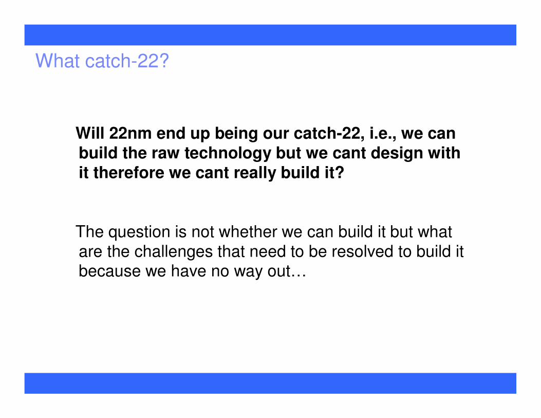
What catch-22?
Will 22nm end up being our catch-22, i.e., we can build the raw technology but we cant design with it therefore we cant really build it?
The question is not whether we can build it but what are the challenges that need to be resolved to build it because we have no way out…

November, 2006 © 2006 IBM Corporation
Back to the Future – ICCAD 2003� Embedded tutorial on:
• Design and CAD Challenges for sub-90nm CMOS Circuits
� Did we predict the challenges?
?� Perfect storm,
coping with:
• Power
• And Variability
� Designing Robust Circuits
• Mitigating variability
Per
form
ance
250nm 180nm 130nm 90nm 65nm 45nm
Area
Delay+Power
+Noise
+Yield/ Robustness
Technology generationTechnology generation250nm 180nm 130nm 90nm 65nm 45nm
Is this worth ahuge investment?
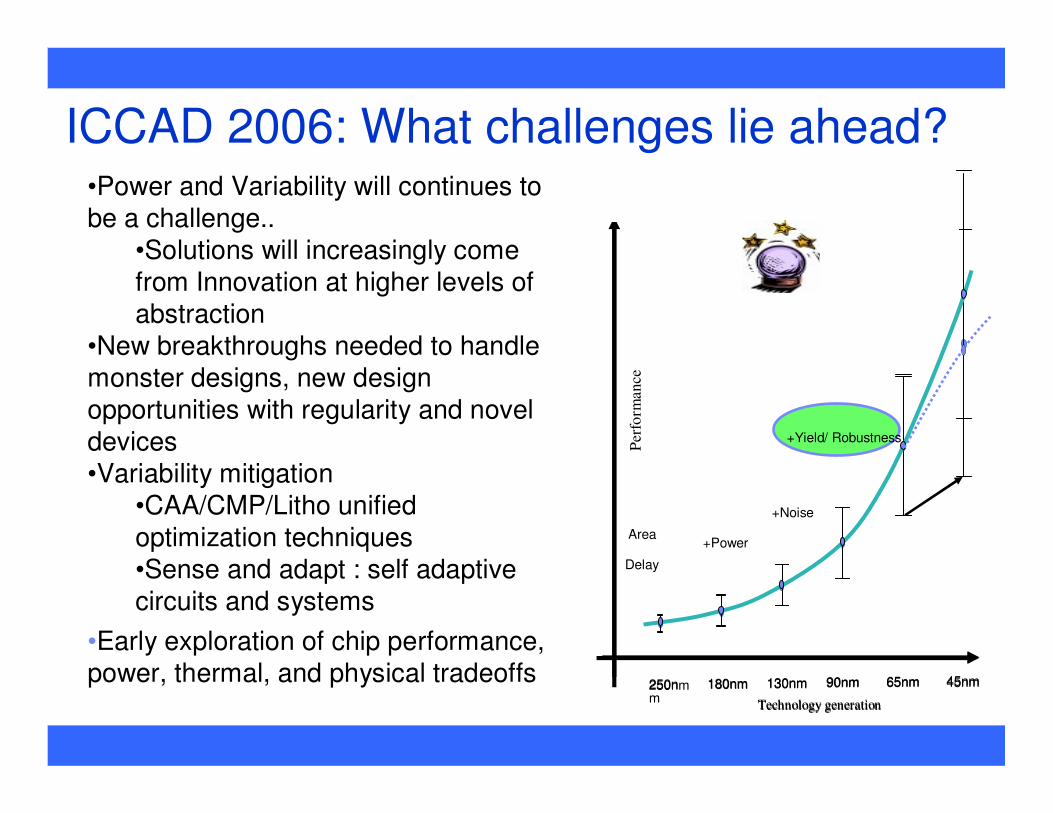
ICCAD 2006: What challenges lie ahead?
?
Per
form
ance
250nm 180nm 130nm 90nm 65nm 45nm
Area
Delay
+Power
+Noise
+Yield/ Robustness
Technology generationTechnology generation
250nm
180nm 130nm 90nm 65nm 45nm
•Power and Variability will continues to be a challenge..
•Solutions will increasingly come from Innovation at higher levels of abstraction
•New breakthroughs needed to handle monster designs, new design opportunities with regularity and novel devices•Variability mitigation
•CAA/CMP/Litho unified optimization techniques•Sense and adapt : self adaptive circuits and systems
•Early exploration of chip performance, power, thermal, and physical tradeoffs
2009: Historic opportunity which is ours to lose
� Technology has been in the driving seat of the semiconductor industry juggernaut but the juggernaut is running out of gas
– Do we really need 22nm?
• Doesn’t buy much performance any more; Painful for power; Variability headaches; Needs lot more people to design
– 300-500 people for 2-3 years to design a complex chip (~200 million $s)
• All the concerns Carl (keynote) brought up..
� Bifurcation of industry into:
• Those who must have 22nm vs those who are happy staying back..
– Specialized solutions needed for different segments
> Analogous to Hybrid computing with accelerators
� Productivity is the driving force now
– It is time to put automation in the driving seat

Topics to discuss..
� Power and Performance..
– Old wine in new bottle, Not going to touch this one.. Traditional issues..
� If we were to survive in this bifurcating industry and be relevant, we have to start doing better at our bread and butter core business
– We cannot afford to build things the way we have been
• Way too costly and painful• Low end designs want more customization to move up and high end designs
want more automation to be efficient• Synthesis, timing, PD, Congestion, Routing, Checking etc.
� ISPD has done outstanding job at driving innovation in placementand now routing; and IWLS at synthesis; and TAU at timing
– The bottleneck lies at their intersection: building things with right timing, that have the desired placement and correct routability.
– We may be ok for 500MHz but we are broken for GHz performance.
– We may be ok for Watts but broken for mWatts
� An eye towards the future..
– 3D (not in the way one thinks about it).
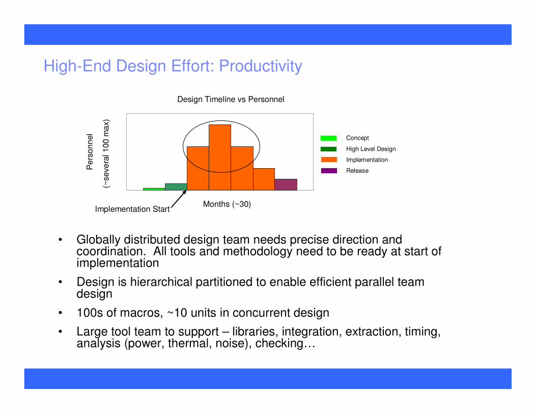
High-End Design Effort: Productivity
• Globally distributed design team needs precise direction and coordination. All tools and methodology need to be ready at start of implementation
• Design is hierarchical partitioned to enable efficient parallel team design
• 100s of macros, ~10 units in concurrent design
• Large tool team to support – libraries, integration, extraction, timing, analysis (power, thermal, noise), checking…
Concept
High Level Design
Implementation
Release
Months (~30)
Pe
rso
nn
el
(~se
ve
ral 1
00
ma
x)Design Timeline vs Personnel
Implementation Start
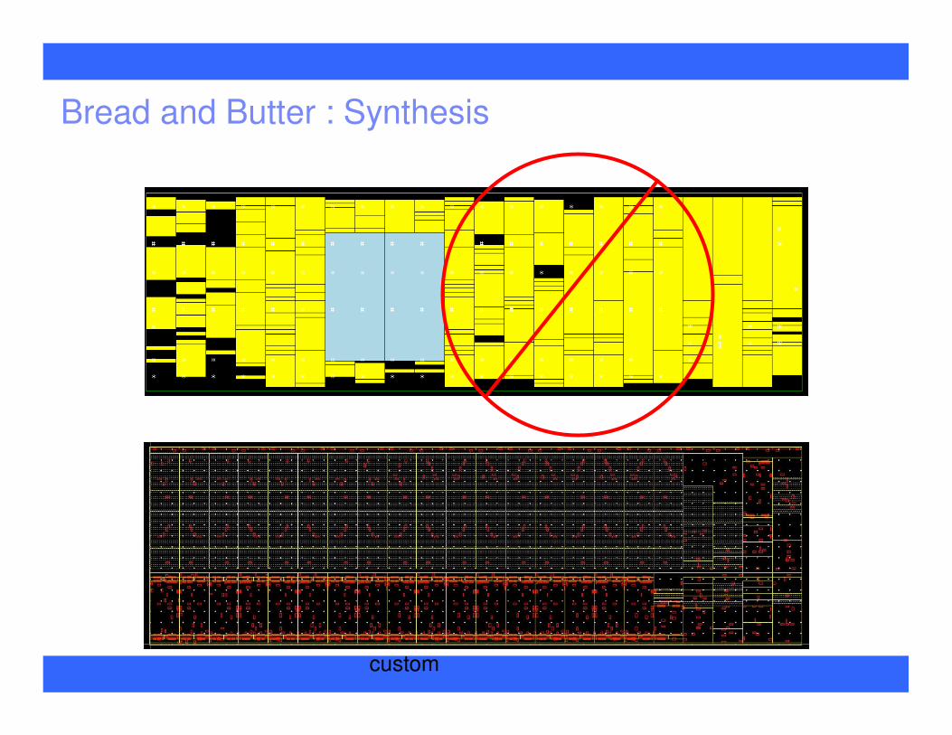
Bread and Butter : Synthesis
custom

Bread and Butter: Synthesis
custom
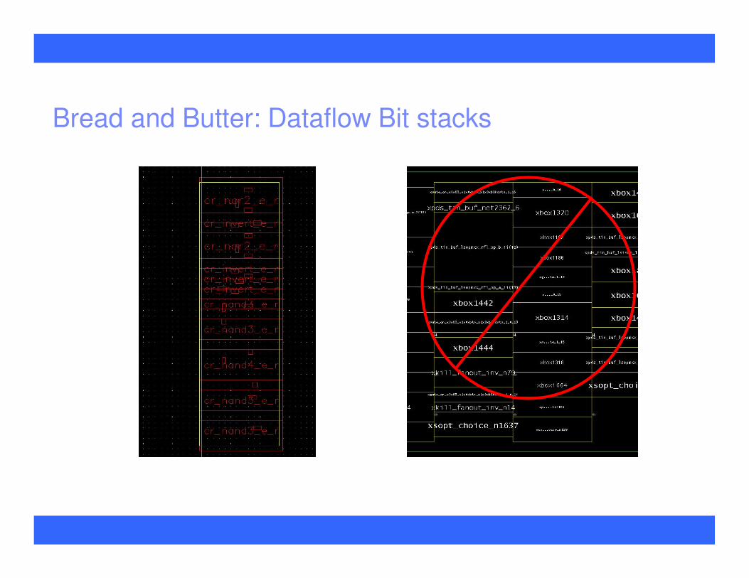
Bread and Butter: Dataflow Bit stacks

Bread and Butter: Synthesized Paths and Routing
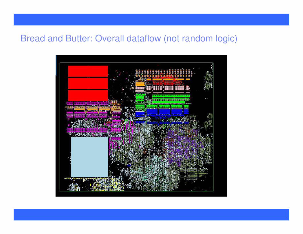
Bread and Butter: Overall dataflow (not random logic)

Bread and Butter: Bottlenecks
� Very reason we will move to 22nm is either:
– Density, or
– Performance (we want even 20% performance)
� If we have to spread things more just to route
– Should we move to 22nm?
� Timing and routing are at cross reads with each other
– A major dilemma – timing wants gates closer – routing wants them spread
� Cant afford it without productivity anyway
– It is the interplay of synthesis, placement, timing, routing which we must address holistically if we want to survive and thrive.
– Must move the manually intensive design portions to automation
– Golden opportunity for Automation and ISPD community.
• Can have real practical impact on the industry
• May not have the appeal of nanotechnology but has lot better chance to see the light of the day
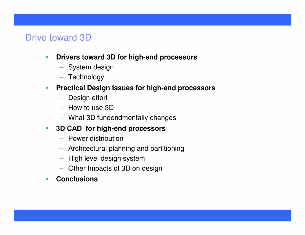
Drive toward 3D
� Drivers toward 3D for high-end processors
– System design
– Technology
� Practical Design Issues for high-end processors
– Design effort
– How to use 3D
– What 3D fundendmentally changes
� 3D CAD for high-end processors
– Power distribution
– Architectural planning and partitioning
– High level design system
– Other Impacts of 3D on design
� Conclusions
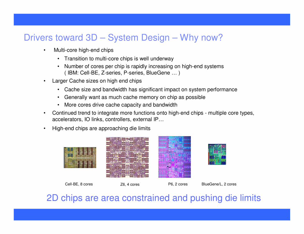
Drivers toward 3D – System Design – Why now?• Multi-core high-end chips
• Transition to multi-core chips is well underway
• Number of cores per chip is rapidly increasing on high-end systems ( IBM: Cell-BE, Z-series, P-series, BlueGene … )
• Larger Cache sizes on high end chips
• Cache size and bandwidth has significant impact on system performance
• Generally want as much cache memory on chip as possible
• More cores drive cache capacity and bandwidth
• Continued trend to integrate more functions onto high-end chips - multiple core types, accelerators, IO links, controllers, external IP…
• High-end chips are approaching die limits
2D chips are area constrained and pushing die limits
Cell-BE, 8 cores Z6, 4 cores P6, 2 cores BlueGene/L, 2 cores
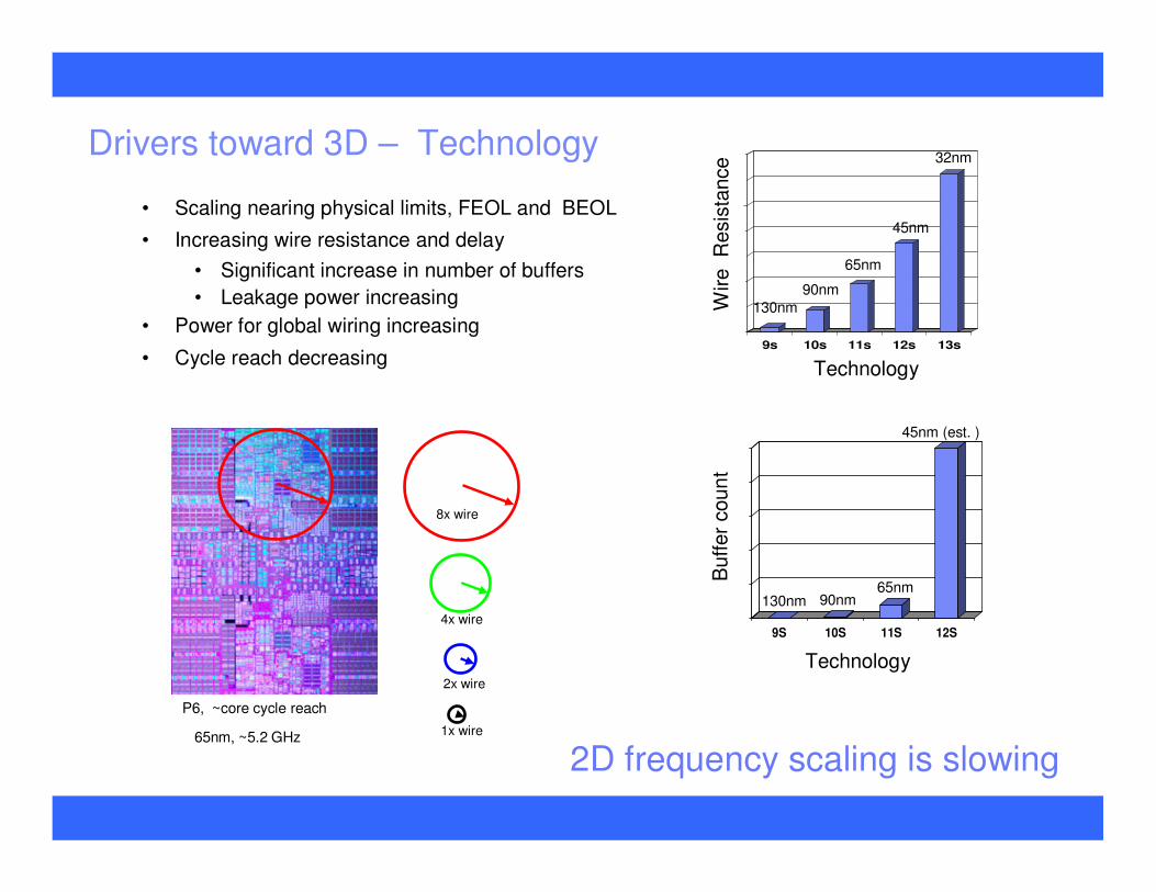
Drivers toward 3D – Technology
• Scaling nearing physical limits, FEOL and BEOL
• Increasing wire resistance and delay
• Significant increase in number of buffers
• Leakage power increasing
• Power for global wiring increasing
• Cycle reach decreasing
2D frequency scaling is slowing
9s 10s 11s 12s 13s
Wire R
esis
tance
130nm90nm
65nm
45nm
32nm
Technology
9S 10S 11S 12S
130nm 90nm65nm
45nm (est. )
Buffer
coun
t
Technology
P6, ~core cycle reach
65nm, ~5.2 GHz
2x wire
4x wire
8x wire
1x wire
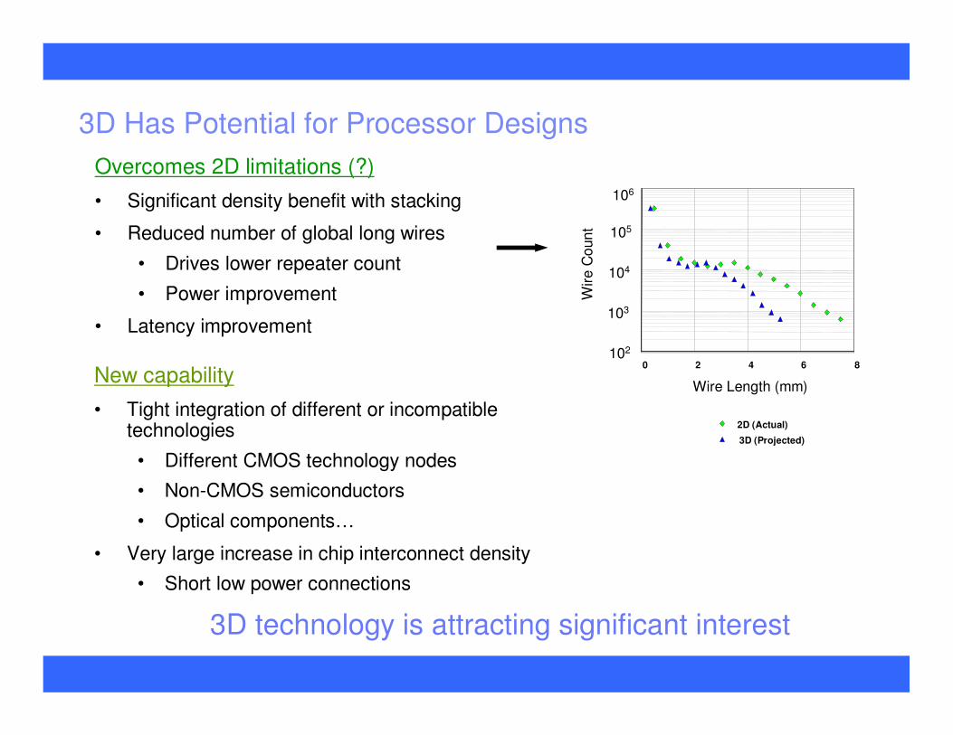
Overcomes 2D limitations (?)
• Significant density benefit with stacking
• Reduced number of global long wires
• Drives lower repeater count
• Power improvement
• Latency improvement
3D Has Potential for Processor Designs
3D technology is attracting significant interest
New capability
• Tight integration of different or incompatible technologies
• Different CMOS technology nodes
• Non-CMOS semiconductors
• Optical components…
• Very large increase in chip interconnect density
• Short low power connections
0 2 4 6 8
Wire Length (mm)
Wir
e C
oun
t
2D (Actual)
3D (Projected)
103
104
102
105
106
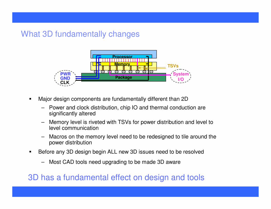
What 3D fundamentally changes
Package
Memory
Processor
PWRGNDCLK
System I/O
TSVs
� Major design components are fundamentally different than 2D
– Power and clock distribution, chip IO and thermal conduction aresignificantly altered
– Memory level is riveted with TSVs for power distribution and level to level communication
– Macros on the memory level need to be redesigned to tile around the power distribution
� Before any 3D design begin ALL new 3D issues need to be resolved
– Most CAD tools need upgrading to be made 3D aware
3D has a fundamental effect on design and tools

Power Distribution Challenges
Gnd
Power
Signal
• 2D power distribution is highly varied
• Core regions at peak capacity
• Other regions are underutilized
• Multiple power domains are required
• Vdd, Vcs, Vdr, Vanalog, Vio, …
• Horizontal distributed adds large IR drop
• Power increase from IR drop } to �V3
• 3D power densities will be significantly larger
• Non-uniform power could exacerbate current irregularity
• Power domains may be stacked coincident
• Power transport though intermediate stack
• Adds additional IR drop
• Force tiling around power TSVs
2D Ground Current Distribution
y
X
current
3D Design partitioning Level
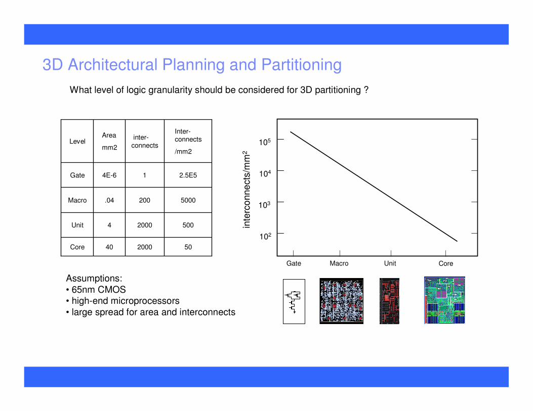
3D Architectural Planning and Partitioning
inte
rco
nne
cts
/mm
2
Gate Macro Unit Core
103
104
102
105
What level of logic granularity should be considered for 3D partitioning ?
2000
2000
200
1
inter-connects
50
500
5000
2.5E5
Inter-connects
/mm2
Area
mm2Level
40Core
4Unit
.04Macro
4E-6Gate
Assumptions:• 65nm CMOS• high-end microprocessors• large spread for area and interconnects

3D Design partitioning Level
3D Architectural Planning and Partitioning
% Area Overhead for Interconnects
Reasonable partition granularity depends strongly on via size
• Area for power TSVs not included. • ~5-10 % area, depends on IR drop and EM targets• Did not include “keepout” around via
• Chip performance is generally limited by global paths at core/unit level. • For global wire length improvement AND reuse, 3D partitioning at core level above
0.001
0.01
0.12
5
20.50.120.01
2021.20.05
20050120.5
8000200050020
0.5
Via Diameter (�m)
201051
Core
unit
macro
gate
Part
ition
Leve
l

• It is essential to study 2D, 3D options very early in the design cycle
• Early analysis tools should allow study of tradeoffs between layer count, partitioning options, floorplans, power density, performance and cost
• Requires strong link between architectural level analysis tools and 3D physical planning tools.
• Increased circuit density of 3D IC leads to increased power density:
• Development of “thermally aware” design tools• Partition design to place highly loaded, active components in
layer close to the heat-sink
• Research must focus on Early Analysis Framework Tool
3D Architectural Planning, Analysis and Integration Framework
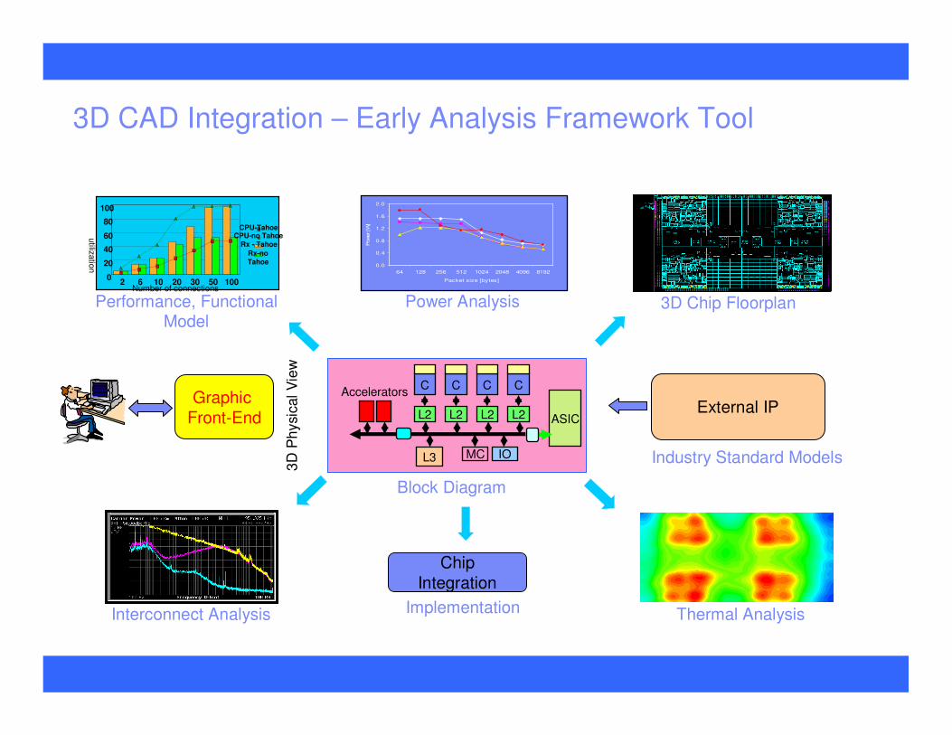
3D CAD Integration – Early Analysis Framework Tool
0.0
0.4
0.8
1.2
1.6
2.0
64 128 256 512 1024 2048 4096 8192
Packet size [bytes]
Power [W
]
Power Analysis 3D Chip FloorplanPerformance, Functional Model
2 6 10 20 30 50 100Number of connections
0
20
40
60
80
100
utiliza
tion
CPU-TahoeCPU-no Tahoe
Rx - Tahoe
Rx-no Tahoe
Interconnect Analysis Thermal Analysis
Graphic Front-End
External IP
ChipIntegration
Implementation
Industry Standard Models
C
L2
C
L2
C
L2
C
L2
L3 MC IO
Accelerators
ASIC
Block Diagram
3D
Ph
ysi
cal V
iew

What does 3D fundamentally change
Package
Memory
Processor
PWRGNDCLK
System I/O
TSVs
� This partitioning preserves the high value core basically intact for reuse in 2D systems
� Major design components are fundamentally different than 2D
– Power and clock distribution, chip IO and thermal conduction are significantly altered
– Memory level is riveted with TSVs for power distribution and level to level communication
– Macros on the memory level need to be redesigned to tile around the power distribution
� Before any 3D design begin ALL new 3D issues need to be resolved
– Most CAD tools need upgrading to be made 3D aware

November, 2006 © 2006 IBM Corporation
How to predict the Future: by Scott Adams in “The Dilbert Future”�Some people try to predict the future by assuming
current trends will continue…….
If you applied that forecasting method to a puppy, you'd predict that the puppy would continue growing larger and larger until….
But that rarely happens, thanks to the National Guard.
one day… in a fit of uncontrolled happiness… its wagging tail would destroy a major metropolitan area.

Conclusions
� Will 22nm be catch-22
– If we don’t take advantage of the opportunity
• It will be a catch-22 for most
� Need to move away from appeal of nano to bread and butter of PD
– 500Mhz to GHz; Watts to mW
� 3D – exciting opportunity for certain segments; Many Design and CAD challenges
� The future could be exciting and the opportunity is unprecedented due to confluence of various factors including current financial crisis.
– What we do with this is in our hands