WIDE INPUT VOLTAGE RANGE, 150mA ULDO … · WIDE INPUT VOLTAGE RANGE, 150mA ULDO ... 1 2 2 VIN...
12
AP7380 Document number: DS39196 Rev. 3 - 2 1 of 12 www.diodes.com December 2017 © Diodes Incorporated AP7380 NEW PRODUCT WIDE INPUT VOLTAGE RANGE, 150mA ULDO REGULATOR Description The AP7380 series is a positive voltage regulator IC. The AP7380 has features of wide input voltage range, high accuracy, low dropout voltage, current limit and ultra-low quiescent current which make it ideal for use in various USB and portable devices and instrument application. The IC consists of a voltage reference, an error amplifier, a resistor network for setting output voltage, a current limit circuit for current protection, and a chip enable circuit. The AP7380 is available in 1.8V, 3.0V, 3.3V, 3.6V, 4.15V, 4.4V and 5.0V fixed output voltage versions. The AP7380 is available in space-saving SOT25 and SOT89 (Option 2) packages. Features Wide Input Voltage Range: Up to 24V Low Dropout Voltage: VDROP = 500mV @ IOUT = 50mA Low Ground Current High Output Voltage Accuracy Compatible with Low ESR Ceramic Capacitor Excellent Line/Load Regulation Thermal Shutdown Function Totally Lead-Free & Fully RoHS Compliant (Notes 1 & 2) Halogen and Antimony Free. “Green” Device (Note 3) Applications Battery-powered Equipment Laptop, Palmtops, Notebook Computers Portable Information Appliances Pin Assignments (Top View) SOT89 (Option 2) (Top View) SOT25 (W5 Package) (Top View) SOT25 (WR Package) Notes: 1. No purposely added lead. Fully EU Directive 2002/95/EC (RoHS) & 2011/65/EU (RoHS 2) compliant. 2. See http://www.diodes.com/quality/lead_free.html for more information about Diodes Incorporated’s definitions of Halogen- and Antimony-free, "Green" and Lead-free. 3. Halogen- and Antimony-free "Green” products are defined as those which contain <900ppm bromine, <900ppm chlorine (<1500ppm total Br + Cl) and <1000ppm antimony compounds. 1 2 3 GND VIN VOUT VIN
Transcript of WIDE INPUT VOLTAGE RANGE, 150mA ULDO … · WIDE INPUT VOLTAGE RANGE, 150mA ULDO ... 1 2 2 VIN...
AP7380 Document number: DS39196 Rev. 3 - 2
1 of 12 www.diodes.com
December 2017 © Diodes Incorporated
AP7380
NE
W P
RO
DU
CT
WIDE INPUT VOLTAGE RANGE, 150mA ULDO REGULATOR
Description
The AP7380 series is a positive voltage regulator IC.
The AP7380 has features of wide input voltage range, high accuracy,
low dropout voltage, current limit and ultra-low quiescent current
which make it ideal for use in various USB and portable devices and
instrument application.
The IC consists of a voltage reference, an error amplifier, a resistor
network for setting output voltage, a current limit circuit for current
protection, and a chip enable circuit.
The AP7380 is available in 1.8V, 3.0V, 3.3V, 3.6V, 4.15V, 4.4V and
5.0V fixed output voltage versions.
The AP7380 is available in space-saving SOT25 and SOT89 (Option
2) packages.
Features
Wide Input Voltage Range: Up to 24V
Low Dropout Voltage: VDROP = 500mV @ IOUT = 50mA
Low Ground Current
High Output Voltage Accuracy
Compatible with Low ESR Ceramic Capacitor
Excellent Line/Load Regulation
Thermal Shutdown Function
Totally Lead-Free & Fully RoHS Compliant (Notes 1 & 2)
Halogen and Antimony Free. “Green” Device (Note 3)
Applications
Battery-powered Equipment
Laptop, Palmtops, Notebook Computers
Portable Information Appliances
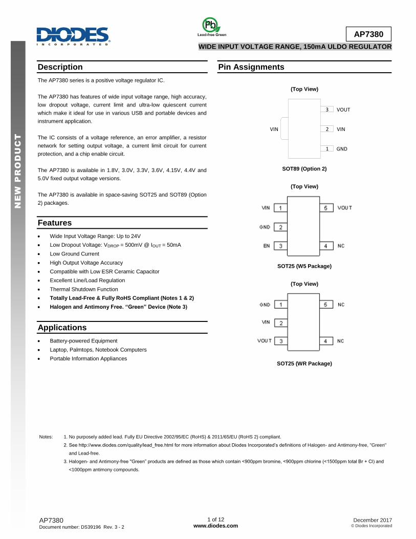
Pin Assignments
(Top View)
SOT89 (Option 2)
(Top View)
SOT25 (W5 Package)
(Top View)
SOT25 (WR Package)
Notes: 1. No purposely added lead. Fully EU Directive 2002/95/EC (RoHS) & 2011/65/EU (RoHS 2) compliant.
2. See http://www.diodes.com/quality/lead_free.html for more information about Diodes Incorporated’s definitions of Halogen- and Antimony-free, "Green"
and Lead-free.
3. Halogen- and Antimony-free "Green” products are defined as those which contain <900ppm bromine, <900ppm chlorine (<1500ppm total Br + Cl) and
<1000ppm antimony compounds.
1
2
3
GND
VIN
VOUT
VIN

AP7380 Document number: DS39196 Rev. 3 - 2
2 of 12 www.diodes.com
December 2017 © Diodes Incorporated
AP7380
NE
W P
RO
DU
CT
Typical Applications Circuit
Pin Descriptions
Pin Number
Pin Name Function SOT25 (W5) SOT25 (WR) SOT89 (Option 2)
1 2 2 VIN Input voltage
2 1 1 GND Ground
3 — — EN Enable input
4 4, 5 — NC No connected for fixed version
5 3 3 VOUT Regulated output voltage
SOT89 (Option 2)

AP7380 Document number: DS39196 Rev. 3 - 2
3 of 12 www.diodes.com
December 2017 © Diodes Incorporated
AP7380
NE
W P
RO
DU
CT
Absolute Maximum Ratings
Symbol Parameter Rating Unit
VIN Supply Input Voltage 30 V
VEN Enable Input Voltage 30 V
IOUT Output Current 200 mA
TLEAD Lead Temperature (Soldering, 10sec) +260 °C
TJ Operating Junction Temperature +150 °C
θJA Thermal Resistance (Junction to Ambient)
SOT25 (W5) 193
°C/W SOT25 (WR) 166
SOT89 (Option 2) 118
θJC Thermal Resistance (Junction to Case)
SOT25 (W5) 68
°C/W SOT25 (WR) 26
SOT89 (Option 2) 20
TSTG Storage Temperature Range -65 to +150 °C
— ESD (Machine Model) 250 V
— ESD (Human Body Model) 2500 V
Recommended Operating Conditions
Symbol Parameter Min Max Unit
VIN Supply Input Voltage 3.5 24 V
TJ Operating Junction Temperature -40 +125 °C

AP7380 Document number: DS39196 Rev. 3 - 2
4 of 12 www.diodes.com
December 2017 © Diodes Incorporated
AP7380
NE
W P
RO
DU
CT
Electrical Characteristics (@ VIN = VOUT + 2V, CIN = 1.0µF, COUT = 1.0µF, Typical TJ = +25°C, unless otherwise specified.)
Symbol Parameter Test Conditions Min Typ Max Unit
VOUT Output Voltage VIN = VOUT + 2V, IOUT = 10mA
Variation from Specified VOUT VOUTx99% VOUT VOUTx101% V
VIN Input Voltage — 3.5 — 24 V
ILIMIT Current Limit VIN = VOUT + 2V, VOUT1 = 98% x VOUT 150 — — mA
∆VOUT/∆VIN/VOUT Line Regulation VOUT + 2V ≤ VIN ≤ 24V, IOUT = 10mA — 0.05 — %/V
∆VOUT/VOUT Load Regulation VIN = VOUT + 2V, 1mA ≤ IOUT ≤ 150mA — 0.5 — %
VDROP Dropout Voltage
3.0V VOUT < 5.0V
IOUT = 50mA — 360 580 mV
IOUT = 100mA — 750 1000 mV
IOUT = 150mA — 1050 1500 mV
VOUT = 5.0V
IOUT = 50mA — 250 500 mV
IOUT = 100mA — 550 750 mV
IOUT = 150mA — 750 1100 mV
IGND Ground Current
IOUT = 0A — 1.8 3.0
µA
IOUT = 150mA — 1.8 3.0
ISTD Standby Current VEN in OFF Mode — 0.01 — µA
∆VOUT/(VOUTx∆T) Output Voltage Temperature Coefficient IOUT = 100µA, -40°C ≤ TJ ≤ +125°C — ±100 — ppm/°C
IEN EN Pin Current — — 1 — µA
— EN “High” Voltage EN Input Voltage “High” 2.0 — — V
— EN “Low” Voltage EN Input Voltage “Low” — — 0.4 V
TOTSD Thermal Shutdown Temperature — — +160 — °C
THYOTSD Thermal Shutdown Hysteresis — — +20 — °C

AP7380 Document number: DS39196 Rev. 3 - 2
5 of 12 www.diodes.com
December 2017 © Diodes Incorporated
AP7380
NE
W P
RO
DU
CT
Performance Characteristics
Output Voltage vs. Input Voltage @-40°C Output Voltage vs. Input Voltage @+25°C
Output Voltage vs. Input Voltage @+85°C Output Voltage vs. Output Current
Output Voltage vs. Temperature Output Voltage vs. Output Current
0 4 8 12 16 20 240.0
0.5
1.0
1.5
2.0
2.5
3.0
3.5
AP7380-30W5
TA=-40
OC
IOUT
=10mA
IOUT
=50mA
IOUT
=100mA
IOUT
=150mA
Ou
tpu
t V
olta
ge
(V
)
Input Voltage (V)
0 4 8 12 16 20 240.0
0.5
1.0
1.5
2.0
2.5
3.0
3.5
AP7380-30W5
TA=+25
OC
IOUT
=10mA
IOUT
=50mA
IOUT
=100mA
IOUT
=150mA
Ou
tpu
t V
olta
ge
(V
)
Input Voltage (V)
0 4 8 12 16 20 240.0
0.5
1.0
1.5
2.0
2.5
3.0
3.5
AP7380-30W5
TA=+85
OC
IOUT
=10mA
IOUT
=50mA
IOUT
=100mA
IOUT
=150mA
Ou
tpu
t V
olta
ge
(V
)
Input Voltage (V)
0 50 100 150 200 250 300 350 4000.0
0.5
1.0
1.5
2.0
2.5
3.0
3.5
AP7380-30W5
VIN
=4.5V
TA= -40
OC
TA= +25
OC
TA= +85
OC
Ou
tpu
t V
olta
ge
(V
)
Output Current (mA)
0 15 30 45 60 75 90 105 120 135 1502.80
2.85
2.90
2.95
3.00
3.05
3.10
AP7380-30W5
VIN
=4.5V
TA= -40
OC
TA= +25
OC
TA= +85
OC
Ou
tpu
t V
olta
ge
(V
)
Output Current (mA)-40 -25 -10 5 20 35 50 65 80 95 110 125
2.80
2.85
2.90
2.95
3.00
3.05
3.10
AP7380-30W5
VIN
=4.5V
IOUT
=10mA
IOUT
=50mA
IOUT
=100mA
IOUT
=150mA
Ou
tpu
t V
olta
ge
(V
)
Temperature (OC)
AP7380 Document number: DS39196 Rev. 3 - 2
6 of 12 www.diodes.com
December 2017 © Diodes Incorporated
AP7380
NE
W P
RO
DU
CT
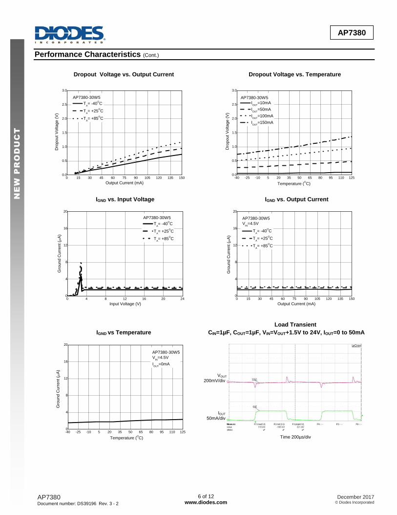
Performance Characteristics (Cont.)
Dropout Voltage vs. Output Current Dropout Voltage vs. Temperature
IGND vs. Input Voltage IGND vs. Output Current
Load Transient
IGND vs Temperature CIN=1µF, COUT=1µF, VIN=VOUT+1.5V to 24V, IOUT=0 to 50mA
0 4 8 12 16 20 240
4
8
12
16
20
AP7380-30W5
TA= -40
OC
TA= +25
OC
TA= +85
OC
Gro
un
d C
urr
en
t (
A)
Input Voltage (V)
0 15 30 45 60 75 90 105 120 135 1500
4
8
12
16
20
AP7380-30W5
VIN
=4.5V
TA= -40
OC
TA= +25
OC
TA= +85
OC
Gro
un
d C
urr
en
t (
A)
Output Current (mA)
-40 -25 -10 5 20 35 50 65 80 95 110 1250
4
8
12
16
20
AP7380-30W5
VIN
=4.5V
IOUT
=0mA
Gro
un
d C
urr
en
t (
A)
Temperature (OC)
0 15 30 45 60 75 90 105 120 135 1500.0
0.5
1.0
1.5
2.0
2.5
3.0
AP7380-30W5
TA= -40
OC
TA= +25
OC
TA= +85
OC
Dro
po
ut V
olta
ge
(V
)
Output Current (mA)
-40 -25 -10 5 20 35 50 65 80 95 110 1250.0
0.5
1.0
1.5
2.0
2.5
3.0
AP7380-30W5
IOUT
=10mA
IOUT
=50mA
IOUT
=100mA
IOUT
=150mA
Dro
po
ut V
olta
ge
(V
)
Temperature (OC)
VOUT 200mV/div
IOUT 50mA/div
Time 200µs/div

AP7380 Document number: DS39196 Rev. 3 - 2
7 of 12 www.diodes.com
December 2017 © Diodes Incorporated
AP7380
NE
W P
RO
DU
CT
Ordering Information
AP7380 - X X - X
Packing
7/13 : Tape & Reel
Output Voltage
18 : 1.8V
30 : 3.0V
33 : 3.3V
36 : 3.6V
41 : 4.15V
44 : 4.4V
50 : 5.0V
W5/WR : SOT25
Y : SOT89 (Option 2)
Package
Part Number Package Code Package 7”/13” Tape and Reel
Quantity Part Number Suffix
AP7380-18W5-7 W5 SOT25 3000/Tape & Reel -7
AP7380-30W5-7 W5 SOT25 3000/Tape & Reel -7
AP7380-33W5-7 W5 SOT25 3000/Tape & Reel -7
AP7380-36W5-7 W5 SOT25 3000/Tape & Reel -7
AP7380-41W5-7 W5 SOT25 3000/Tape & Reel -7
AP7380-44W5-7 W5 SOT25 3000/Tape & Reel -7
AP7380-50W5-7 W5 SOT25 3000/Tape & Reel -7
AP7380-18WR-7 WR SOT25 3000/Tape & Reel -7
AP7380-30WR-7 WR SOT25 3000/Tape & Reel -7
AP7380-33WR-7 WR SOT25 3000/Tape & Reel -7
AP7380-36WR-7 WR SOT25 3000/Tape & Reel -7
AP7380-41WR-7 WR SOT25 3000/Tape & Reel -7
AP7380-44WR-7 WR SOT25 3000/Tape & Reel -7
AP7380-50WR-7 WR SOT25 3000/Tape & Reel -7
AP7380-18Y-13 Y SOT89 (Option 2) 2500/Tape & Reel -13
AP7380-30Y-13 Y SOT89 (Option 2) 2500/Tape & Reel -13
AP7380-33Y-13 Y SOT89 (Option 2) 2500/Tape & Reel -13
AP7380-36Y-13 Y SOT89 (Option 2) 2500/Tape & Reel -13
AP7380-41Y-13 Y SOT89 (Option 2) 2500/Tape & Reel -13
AP7380-44Y-13 Y SOT89 (Option 2) 2500/Tape & Reel -13
AP7380-50Y-13 Y SOT89 (Option 2) 2500/Tape & Reel -13

AP7380 Document number: DS39196 Rev. 3 - 2
8 of 12 www.diodes.com
December 2017 © Diodes Incorporated
AP7380
NE
W P
RO
DU
CT
Marking Information
(1) SOT25
1 2 3
5 74
(Top View)
XXX : Identification Code
W : Week : A to Z : 1 to 26 week;
X : Internal Code
Y : Year 0 to 9
a to z : 27 to 52 week; z represents52 and 53 week
XXX
Y W X
Part Number Package Identification Code
AP7380-18W5-7 SOT25 D8M
AP7380-30W5-7 SOT25 D8E
AP7380-33W5-7 SOT25 D8A
AP7380-36W5-7 SOT25 D8P
AP7380-41W5-7 SOT25 D8F
AP7380-44W5-7 SOT25 D8G
AP7380-50W5-7 SOT25 D8B
AP7380-18WR-7 SOT25 D8N
AP7380-30WR-7 SOT25 D8H
AP7380-33WR-7 SOT25 D8C
AP7380-36WR-7 SOT25 D8R
AP7380-41WR-7 SOT25 D8J
AP7380-44WR-7 SOT25 D8K
AP7380-50WR-7 SOT25 D8D
(2) SOT89 (Option 2)
XXX
Y W X
XXX : Identification code
(Top View)
Y : Year : 0~9
W : Week : A~Z : 1~26 week;
X : Internal code
a~z : 27~52 week;z represents 52 and 53 week
1 2 3
Part Number Package Identification Code
AP7380-18Y-13 SOT89 (Option 2) D8M
AP7380-30Y-13 SOT89 (Option 2) D8E
AP7380-33Y-13 SOT89 (Option 2) D8A
AP7380-36Y-13 SOT89 (Option 2) D8P
AP7380-41Y-13 SOT89 (Option 2) D8F
AP7380-44Y-13 SOT89 (Option 2) D8G
AP7380-50Y-13 SOT89 (Option 2) D8B

AP7380 Document number: DS39196 Rev. 3 - 2
9 of 12 www.diodes.com
December 2017 © Diodes Incorporated
AP7380
NE
W P
RO
DU
CT
Package Outline Dimensions (All dimensions in mm.)
(1) Package Type: SOT89
45
1.550(0.061)REF
4.400(0.173)
4.600(0.181)
0.900(0.035)
1.200(0.047)
3.950(0.156)
4.250(0.167)
3.000(0.118)
TYP
0.480(0.019)
2.300(0.091)
2.600(0.102)
0.320(0.013)
0.540(0.021)
3 10
2.060(0.081)REF
1.400(0.055)
1.600(0.063)
0.350(0.014)
0.450(0.018)
R0.150(0.006)
3
10
1.500(0.059)
0.320(0.013)REF
1.620(0.064)REF2.210(0.087)REF
0.320(0.013)
0.540(0.021)
1.800(0.071)
Option 1 Option 2
0.620(0.024)
1.030(0.041)REF R 0.200(0.008)
1.620(0.064)
1.830(0.072)
2.630(0.104)
2.930(0.115)
Option 1

AP7380 Document number: DS39196 Rev. 3 - 2
10 of 12 www.diodes.com
December 2017 © Diodes Incorporated
AP7380
NE
W P
RO
DU
CT
Package Outline Dimensions (Cont.)
Please see http://www.diodes.com/package-outlines.html for the latest version.
(2) Package Type: SOT25
Suggested Pad Layout
Please see http://www.diodes.com/package-outlines.html for the latest version.
(1) Package Type: SOT25
SOT25
Dim Min Max Typ
A 0.35 0.50 0.38
B 1.50 1.70 1.60
C 2.70 3.00 2.80
D - - 0.95
H 2.90 3.10 3.00
J 0.013 0.10 0.05
K 1.00 1.30 1.10
L 0.35 0.55 0.40
M 0.10 0.20 0.15
N 0.70 0.80 0.75
0° 8° -
All Dimensions in mm
Dimensions Value
Z 3.20
G 1.60
X 0.55
Y 0.80
C1 2.40
C2 0.95
A
M
JLD
B C
H
KN
X
Z
Y
C1
C2C2
G
AP7380 Document number: DS39196 Rev. 3 - 2
11 of 12 www.diodes.com
December 2017 © Diodes Incorporated
AP7380
NE
W P
RO
DU
CT
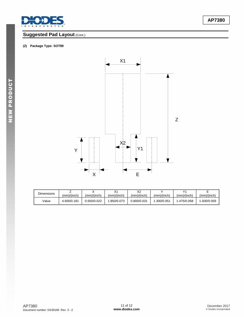
Suggested Pad Layout (Cont.)
(2) Package Type: SOT89
X1
X2
Y1
EX
Y
Z
Dimensions Z
(mm)/(inch) X
(mm)/(inch) X1
(mm)/(inch) X2
(mm)/(inch) Y
(mm)/(inch) Y1
(mm)/(inch) E
(mm)/(inch)
Value 4.600/0.181 0.550/0.022 1.850/0.073 0.800/0.031 1.300/0.051 1.475/0.058 1.500/0.059
AP7380 Document number: DS39196 Rev. 3 - 2
12 of 12 www.diodes.com
December 2017 © Diodes Incorporated
AP7380
NE
W P
RO
DU
CT
IMPORTANT NOTICE DIODES INCORPORATED MAKES NO WARRANTY OF ANY KIND, EXPRESS OR IMPLIED, WITH REGARDS TO THIS DOCUMENT, INCLUDING, BUT NOT LIMITED TO, THE IMPLIED WARRANTIES OF MERCHANTABILITY AND FITNESS FOR A PARTICULAR PURPOSE (AND THEIR EQUIVALENTS UNDER THE LAWS OF ANY JURISDICTION). Diodes Incorporated and its subsidiaries reserve the right to make modifications, enhancements, improvements, corrections or other changes without further notice to this document and any product described herein. Diodes Incorporated does not assume any liability arising out of the application or use of this document or any product described herein; neither does Diodes Incorporated convey any license under its patent or trademark rights, nor the rights of others. Any Customer or user of this document or products described herein in such applications shall assume all risks of such use and will agree to hold Diodes Incorporated and all the companies whose products are represented on Diodes Incorporated website, harmless against all damages. Diodes Incorporated does not warrant or accept any liability whatsoever in respect of any products purchased through unauthorized sales channel. Should Customers purchase or use Diodes Incorporated products for any unintended or unauthorized application, Customers shall indemnify and hold Diodes Incorporated and its representatives harmless against all claims, damages, expenses, and attorney fees arising out of, directly or indirectly, any claim of personal injury or death associated with such unintended or unauthorized application. Products described herein may be covered by one or more United States, international or foreign patents pending. Product names and markings noted herein may also be covered by one or more United States, international or foreign trademarks. This document is written in English but may be translated into multiple languages for reference. Only the English version of this document is the final and determinative format released by Diodes Incorporated.
LIFE SUPPORT Diodes Incorporated products are specifically not authorized for use as critical components in life support devices or systems without the express written approval of the Chief Executive Officer of Diodes Incorporated. As used herein: A. Life support devices or systems are devices or systems which: 1. are intended to implant into the body, or
2. support or sustain life and whose failure to perform when properly used in accordance with instructions for use provided in the labeling can be reasonably expected to result in significant injury to the user.
B. A critical component is any component in a life support device or system whose failure to perform can be reasonably expected to cause the failure of the life support device or to affect its safety or effectiveness. Customers represent that they have all necessary expertise in the safety and regulatory ramifications of their life support devices or systems, and acknowledge and agree that they are solely responsible for all legal, regulatory and safety-related requirements concerning their products and any use of Diodes Incorporated products in such safety-critical, life support devices or systems, notwithstanding any devices- or systems-related information or support that may be provided by Diodes Incorporated. Further, Customers must fully indemnify Diodes Incorporated and its representatives against any damages arising out of the use of Diodes Incorporated products in such safety-critical, life support devices or systems. Copyright © 2017, Diodes Incorporated www.diodes.com