Welcome to NANO 52. Course Objective... To introduce nanostructures and nanomaterials studied and...
22
Welcome to NANO 52
-
Upload
cynthia-wells -
Category
Documents
-
view
216 -
download
0
Transcript of Welcome to NANO 52. Course Objective... To introduce nanostructures and nanomaterials studied and...
Welcome to
NANO 52

Course Objective...To introduce nanostructures and nanomaterials studied and developed for applications in the emerging fields of nanoscience and nanotechnology.You will learn about:• nanomaterial structure• how structure dictates properties• how processing can change structure
This course will help you to:• use nanomaterials properly• realize new design opportunities
with nanomaterials and nanostructures

Meet your professor…
Dr. Jill JohnsenPhysics, Materials Engineering, & Nanotechnology
Math and Science Teacher Education
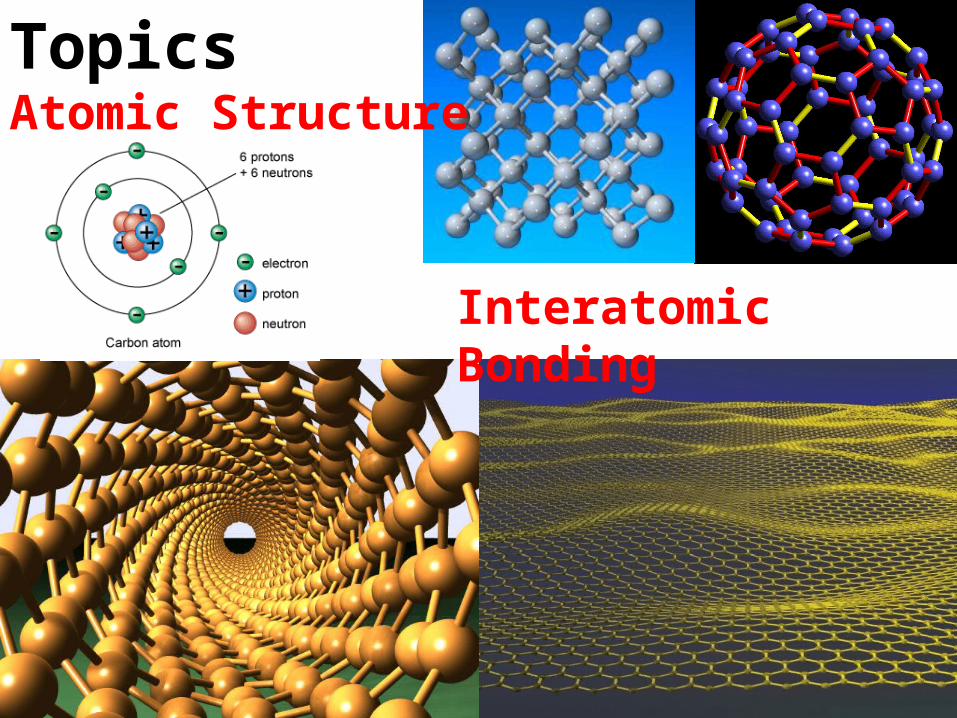
Interatomic Bonding
TopicsAtomic Structure
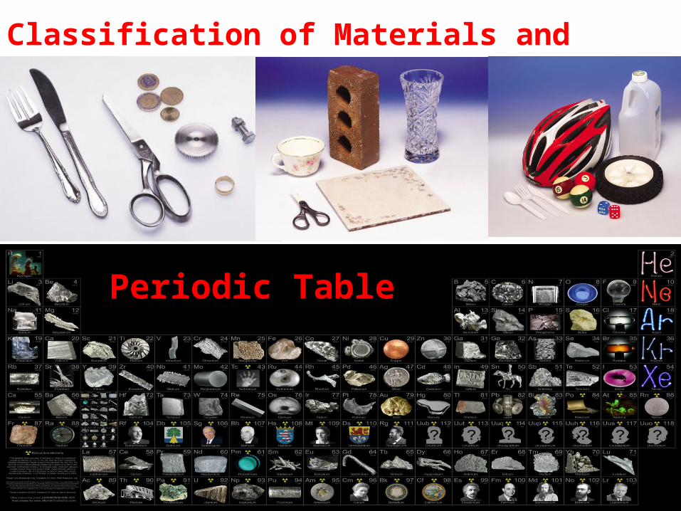
Periodic Table
Classification of Materials and Nanomaterials
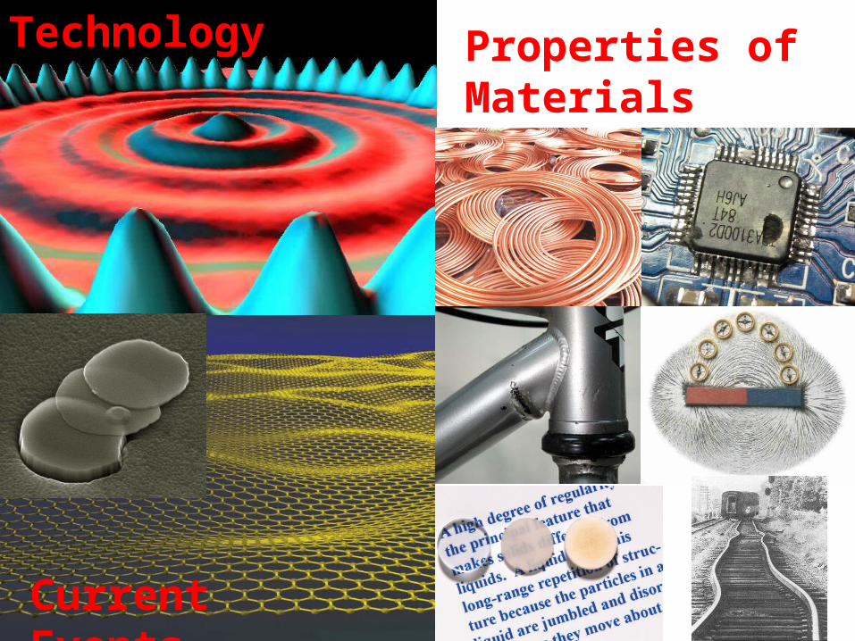
Technology
Current Events
Properties of Materials

Characterization Fabrication
Nanobio-materials
Grain size and Structure

Five Course Nano Program
• NANO 50 – Introduction to Nanotechnology• NANO 51 – Applications of Nanotechnology• NANO 52 – Nanostructures• NANO 53 – Nanocharacterization• NANO 54 – Nanofabrication• Internship (NASA Ames, Stanford)

http://fgamedia.org/faculty/rdcormia/NANO52/
-Syllabus-Weekly homework assignments-Weekly readings-PowerPoint slides from lecture
Course Website:
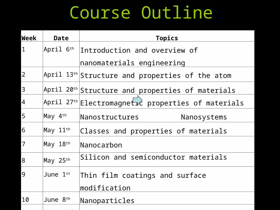
Course OutlineWeek Date Topics
1 April 6th Introduction and overview of nanomaterials engineering
2 April 13th Structure and properties of the atom
3 April 20th Structure and properties of materials
4 April 27th Electromagnetic properties of materials
5 May 4th Nanostructures Nanosystems
6 May 11th Classes and properties of materials
7 May 18th Nanocarbon
8 May 25th Silicon and semiconductor materials
9 June 1st Thin film coatings and surface modification
10 June 8th Nanoparticles
11 June 15th Nanomagnetics
12 June 22nd Novel nanomaterials

Course Outline
I am in the process of scheduling:
Guest Presenters from NASA, Stanford CPN, UC Santa Cruz, Nanolab Technologies, SJSU.
Tours of Stanford CPN, SNF, SJSU Research Labs, Nanolab Technologies.
AFM demostrations and training at Foothill.
SEM, XPS, and TEM demonstrations and training at NASA Advanced Studies Lab.

Stanford CPN and SNF
http://www.stanford.edu/group/cpn/http://snf.stanford.edu/
NASA ASL
http://asl.ucsc.edu/research.php
http://www.nanolabtechnologies.com/
NanolabTechnologies

Course OutlineWeek Date Topics
1 April 6th Introduction and overview of nanomaterials engineering
2 April 13th Structure and properties of the atom
3 April 20th Structure and properties of materials
4 April 27th Electromagnetic properties of materials
5 May 4th Nanostructures Nanosystems
6 May 11th Classes and properties of materials
7 May 18th Nanocarbon
8 May 25th Silicon and semiconductor materials
9 June 1st Thin film coatings and surface modification
10 June 8th Nanoparticles
11 June 15th Nanomagnetics
12 June 22nd Novel nanomaterials
Take-home midterm due
Final writing assignment due

Grading
Discussion Questions 25 %Weekly Homework Assignments
25 %
Take Home Midterm 25 %Final Writing Assignment 25 %
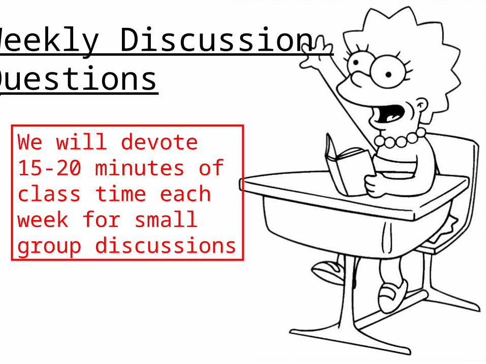
Weekly Discussion Questions
We will devote 15-20 minutes of class time each week for small group discussions

Due every Wednesday!
Weekly Homework AssignmentsYou will be asked to answer one or two questions or solve problems related to the topics discussed during class that week.
Please bring your responses to lecture the following week or submit them via email to [email protected] by the following lecture.

The midterm will be based on in-class lectures, reading assignments, and problem sets. The exam will be assigned during week 5 (May 4th) and due in class during week 6 (May 11th).
The midterm will involve both calculation and design problems that may involve web research.
Take-Home Midterm examDue Wednesday May 11th

You will write a final research paper on a nanostructure or technology of your choice.
The paper should reference current literature on your selected topic and should target an audience of your fellow students.
5 to 10 pages double-spaced 10 to 12 point font including tables and images.
More details to follow…
Due June 22nd
Final Writing Assignment

Ten Key Nanostructures
• Thin film and amorphous silicon (PV) – solar energy
• Carbon nanotubes (CNT) / carbon composite materials (aerospace & transportation)
• Surface coatings and SAMs (Self Assembled Monolayers) Sensors and bionanotechnology
• Nitinol™ (biomedical stents) / electropolished alloys
• Thin film and plasma coatings (polyester film) / high performance glazing
• Particles (coated particles) biomedicine / powder metallurgy (lithium batteries)
• Dendrimers (nanochemistry) – biomedical drug delivery
• Polymers and composites / nanoparticle filler - lightweight automotive and aircraft materials
• Silicon materials Micro Electro Mechanical Systems - (MEMS), Lab-on-a-Chip (LOC), DNA microarrays
• Ceramics and electro ceramics / fuel cells - (stationary / mobile power)

PNPA Relationship
• As you look at different nanotechnologies this quarter think about the following:– What are the applications? (A)– What properties are needed? (P)– What are the (nano)structures? (N)– How do you fabricate / process it? (P)

PNPA
Properties (P)
Applications (A)
Process (P)
Nanostructure (N)
Use PNPA to ‘connect’ topics in the four-course series – from A to PNPA