web.cecs.pdx.eduweb.cecs.pdx.edu/~mperkows/CLASS_VHDL_99/2017ZZ... · Web viewRealization of basic...
26
TRIANGULAR SORTER (Memristor – Parallel) Shri kavya Alaparthy
-
Upload
duongtuyen -
Category
Documents
-
view
224 -
download
4
Transcript of web.cecs.pdx.eduweb.cecs.pdx.edu/~mperkows/CLASS_VHDL_99/2017ZZ... · Web viewRealization of basic...

TRIANGULAR SORTER(Memristor – Parallel)
Shri kavya Alaparthy
923357905.
Sindhu Boddireddy
951176634.

Systolic Sorter:
Many computer applications require sorting.Systolic sorter is a high speed sorter and the name systolic is because it uses a repetitive block structure and has a regular data flow.
Implementation:The four input, 4 bit sorter is here created in a parallel computing fashion with Memristors replacing the AND and OR gates and using the thermometer code. The inputs are given in the form of a systolic array where a homogeneous network of tightly coupled basic block/ cells independently computes a partial result as a result of data received from the downstream neighbors, stores the result within itself and passes it to the upstream neighbors. Here we give x0, x1, x2, x3 as inputs each 4 bit wide and we get the sorted outputs at the end as y0, y1, y2, y3 where y0 is the minimum of all the 4 inputs and y3 is the maximum.

Here we are doing the parallel implementation i.e. all the 4 bits of each input gets computed at a time i.e. in the same clock cycle. The AND and OR gates are called four times within a single clock. This has 4 AND and 4 OR gates virtually inside the basic block operating at the same time. So all the 4 bits gets computed at the same time.
Memristor:Memristors are new class of electronic circuits. Memristor, a concatenation of memory and resistor, are type of elements that maintain relation between current and voltage across a two terminal element. Memristor mean the end of silicon era, giving us low power consumption, increased data storage, ability to compute more information.
Introduction:Maxwell gave his powerful equations which indicates the existence of three fundamental elements, namely resistor, capacitor and inductor. Later in 1971, chua in his paper inferred the possibility of memristor as fundamental nonlinear circuit linking magnetic flux and charge.
The resistance of memristor depends on the integral of input at the terminals and as it remembers the amount of current last passed through, it was named as memristor by chua. Hence according to 1971 definition, memristor is the fourth fundamental circuit element after resistor, capacitor and inductor. But this concept of fourth fundamental circuit element was left alone until the birth of nanotechnology.

Background:Memristor is a three-dimensional device whose resistance depends on charge. They form the basic component of ADALINE, a neural network architecture.
In 1968,F.Argall published a paper which showed the results of memristor.
In 1971,chua mathematically predicted the existence of fourth fundamental circuit element.
In 1972,chua and kang published a paper generalizing the theory of memristors and memristive systems.
In between 1994 and 2008,many other devices evolved with chracteristics similar to memristor but only the hp scientists were able to find a relation between their work and memristor proposed by chua.
Device form of memristor was first developed in 2008 by Stanley Williams.
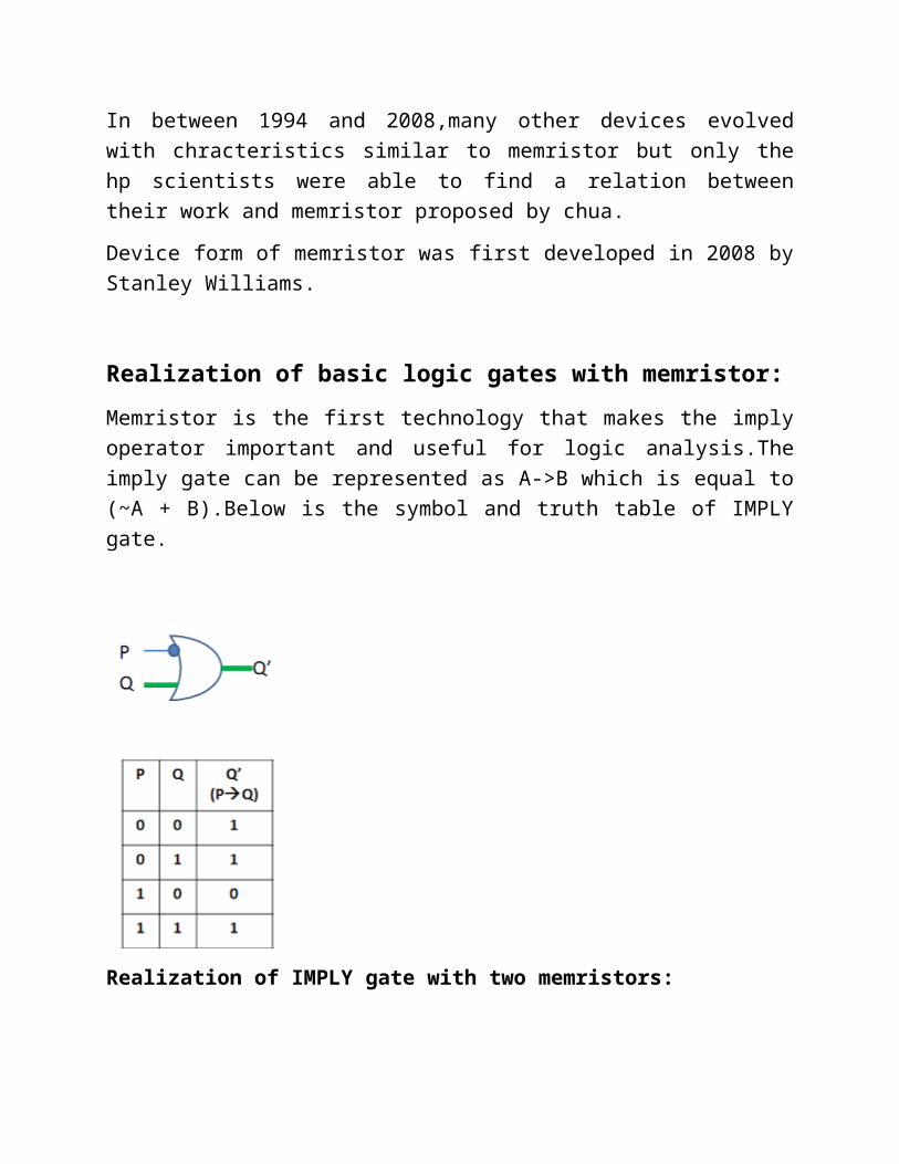
Realization of basic logic gates with memristor:Memristor is the first technology that makes the imply operator important and useful for logic analysis.The imply gate can be represented as A->B which is equal to (~A + B).Below is the symbol and truth table of IMPLY gate.
Realization of IMPLY gate with two memristors:
The above circuit is pulse operated circuit and the source of pulses is are the voltage sources at the top(vcond and vset).Q is called as the working memristor which is set to either 1 or 0 and apart from this two additional pulses are applied with the help of the two voltage sources.
This is the circuit when P=0.This indicates that p is open and has the high resistance which indicates the voltage across the the grounding resistor is “0”.This indicates that the voltage across the working register “Q” is equal to VSET which is greater that VCLOSE and this results in the state of “Q” to be 1 regardless of its initial state.
Now let us study about the working of the circuit when P is not equal to “0”.Below is the circuit diagram.

Now as P is not equal to zero,the resistance across P will be less and hence the voltage across the grounding resistance will be same as VCOND.By this we can say that the voltage across Q will be the difference of VSET and VCOND which is less than VCLOSE .Hence it not possible to switch the state of working resistor “Q” and hence it remains in its same initial state.
Realization of OR gate with memristors:
Implementation of OR gate with memristor requires two working memristors and three pulses.
X = mem (mem (a, 0), B)
Realization of AND gate with memristors:
AND:
X = mem(mem(mem (b,0),a),0)

Sorter dataflow:This design is different from the traditional processor design is because of the min/max topology. Each cell is fed from the bottom by the ColWire with the same indices as the cell itself and similarly on the right by the RowWire with the same indices. The Max/Min outputs are fed to the incremented ColWire and RowWire.
The squares in the diagram above are registers.Cell(0,0) has latency 1. That means the Min/Max outputs of the cell will be valid 1 cycle after the inputs X[0] and X[1] are valid. Cell[1,0] has a latency of 2, which means that it’s Min/Max outputs will be valid 2 cycles after X[0] and X[1] are valid and similarly logic is followed by the remaining cells. Therefore, if X[3] is not delayed for one cycle with respect to X[0] it will arrive at Cell[1,0] too early and will not be compared to it’s data cohorts X[0] and X[1],it will be mistakenly compared to the previous data cohort’s result from Cell[0,0].

The above diagram is showing the data flowing through sorter.
FPGA (Nexys 4 DDR):
In order to calculate power, timing and design area, we used vivado Xilinx to implement the design and then dump it on to the Nexys 4 DDR FPGA. We have used the 16 slider switches as inputs and the 7 segment display as output to display the sorted results. As there are only 16 slider switches, we used 4 inputs of 4 bits each. The module was targeted to the nexys 4 DDR FPGA from digilent. We have used a top module of nexys 4 FPGA where we call the top module of the code and interface the inputs and outputs of code to slider switches and 7 segment display of the board respectively. We also used a debounce module which has all the instantiation’s for slider switches and also the display. After interfacing is done successfully, code is synthesized and then bit stream is generated so that it can be dumped on to FPGA. Vivado has a built in power and delay i.e. timing generator which is used to find the static and dynamic power and setup and hold time delays.

The Nexys4 DDR board is a complete, ready-to-use digital circuit development platform based on the latest Artix-7™ Field Programmable Gate Array (FPGA) from Xilinx®.
With its large, high-capacity FPGA (Xilinx part number XC7A100T-1CSG324C), generous external memories, and collection of USB, Ethernet, and other ports, the Nexys4 DDR can host designs ranging from introductory combinational circuits to powerful embedded processors.
Several built-in peripherals, including an accelerometer, temperature sensor, MEMs digital microphone, a speaker amplifier, and several I/O devices allow the Nexys4 DDR to be used for a wide range of designs without needing any other components.
Timing Diagrams:

These timing diagrams shows how the output is varied at each pulse width.
Here mWideSorter_TB/sort/X is the array of 4 inputs. [3], [2], [1], [0] under it are each input in the input array.
mWideSorter_TB/sort/RowWire is the array of rowwire outputs i.e. the minimum value of each block.These can be analyzed using the array represented below,{(2,3)(2,2,)(2,1)(2,0)}{1,3)(1,2)(1,1)(1,0)} {(0,3)(0,2,)(0,1)(0,0)}Each 4 bit binary number corresponds to the output at each row.
We get the highlighted values in the mWideSorter_TB/sort/RowWire. [2], [1], [0] under it corresponds to {(2,3)(2,2,)(2,1)(2,0)}, { (1,3)(1,2)(1,1)(1,0)}, {(0,3)(0,2,)(0,1)(0,0)} respectively.
mWideSorter_TB/sort/ColWire is the array of colwire outputs i.e. the maximum value of each block.These can be analyzed using the array represented below,{(3,2)(3,1)(3,0)} {(2,2)(2,1)(2,0)} {(1,2)(1,1)(1,0)} {(0,2)(0,1)(0,0)}Each 4 bit binary number corresponds to the output at each column.

We get the highlighted values in the mWideSorter_TB/sort/ColWire.[3], [2], [1], [0] under it corresponds to {(3,2)(3,1)(3,0)}, {(2,2)(2,1)(2,0)}, {(1,2)(1,1)(1,0)}, {(0,2)(0,1)(0,0)} respectively.
mWideSorter_TB/sort/Y is the array of 4 final sorted outputs. [3], [2], [1], [0] under it are each output in the output array.


POWER:

TIMING:
AREA: 0.255mm2 (calculated using the utilization of slices vs available slices).
CODE:
Top Module:
`timescale 1ns/1ps
module mWideSorter_verilog #(
parameter N=4, // individual input width
parameter M=4 // number if inputs
)(
input Clk, Reset,ShifterClr,
input [N-1:0] A,B,C,D,

output [N-1:0] P,Q,R,S
);
integer i; // loop counter
wire [N-1:0] Z [M-1:0];
wire [N-1:0] Xin [M-1:0];
// Cell hookup wires
// [bit-width][row][col]
wire [N-1:0] RowWire [M-2:0][M-1:0];
wire [N-1:0] ColWire [M-1:0][M-2:0];
assign Xin[M-1] = A;
assign Xin[M-2] = B;
assign Xin[M-3] = C;
assign Xin[M-4] = D;
// instantiate and wire up the cells and
// appropriate input/output delays
genvar row, col, j;
generate
// instantiate the cells
for (row=0; row < (M-1); row = row+1) begin
for (col=0; col < (row+1); col = col+1) begin
MinMaxMod_memristor Cell(
.clk (Clk),

.rst (Reset),
.a (ColWire[row][col]),
.b (RowWire[row][col]),
.min (RowWire[row][col+1]),
.max (ColWire[row+1][col])
);
// RowWire[row][col+1] <= dummy_a;
// ColWire[row+1][col] <= dummy_b;
// input delays
if (col===0) begin
if (row===0) begin
Module_verilog #(
.M(1), // one cycle delay
.N(N)
) InDelayX0 (
.Clk(Clk),
.Clr(ShifterClr),
.SI(Xin[0]),
.SO(ColWire[0][0])
);
Module_verilog #(
.M(1), // one cycle delay
.N(N)

) InDelayX1 (
.Clk(Clk),
.Clr(ShifterClr),
.SI(Xin[1]),
.SO(RowWire[0][0])
);
end
else begin
Module_verilog #(
.M(row+1),
.N(N)
) InDelay (
.Clk(Clk),
.Clr(ShifterClr),
.SI(Xin[row+1]),
.SO(RowWire[row][col])
);
end //row===0
end //col===0
// output delays
if (row===M-2) begin
if (col===M-2) begin
Module_verilog #(
.M(1),

.N(N)
) OutDelayYMin (
.Clk(Clk),
.Clr(ShifterClr),
.SI(RowWire[M-2][M-1]),
.SO(Z[M-1])
);
Module_verilog #(
.M(1),
.N(N)
) OutDelayYAlmostMin (
.Clk(Clk),
.Clr(ShifterClr),
.SI(ColWire[M-1][M-2]),
.SO(Z[M-2])
);
end
else begin
Module_verilog #(
.M(row+1),
.N(N)
) OutDelay (
.Clk(Clk),
.Clr(ShifterClr),

.SI(ColWire[row+1][col]),
.SO(Z[col])
);
end //col===M-2
end //row===M-2
end //for col
end //for row
// corner delays
for (j=0; j<M-2; j=j+1) begin
Module_verilog #(
.M(1), // delay one cycle
.N(N)
) CornerDelay (
.Clk(Clk),
.Clr(ShifterClr),
.SI(RowWire[j][j+1]),
.SO(ColWire[j+1][j+1])
);
end
endgenerate
assign P = Z[M-1];
assign Q = Z[M-2];
assign R = Z[M-3];

assign S = Z[M-4];
endmodule
Memristor Module:
`timescale 1ns/1ps
module Mem_verilog #(
parameter N=4)
(
input [N-1:0] neg_inp,
input [N-1:0] mem_inp,
output [N-1:0] mem_out
);
assign mem_out = (~neg_inp) | mem_inp;
endmodule
Min Max module:
`timescale 1ns/1ps
module MinMaxMod_memristor #(
parameter N=4
)(
input clk, rst,
input [N-1:0] a,

input [N-1:0] b,
output reg [N-1:0] min,
output reg [N-1:0] max
);
wire [N-1:0] temp;
wire [N-1:0] temp1;
wire [N-1:0] temp2;
wire [N-1:0] temp3;
wire [N-1:0] temp4;
reg [N-1:0] zero = 0;
always @(posedge clk or posedge rst) begin
if (rst) begin
min <= 0;
max <= 0;
end
else begin
max <= temp1;
min <= temp4;
end
end
Mem_verilog OR1(
.neg_inp(a),
.mem_inp(zero),
.mem_out(temp));

Mem_verilog OR2(
.neg_inp(temp),
.mem_inp(b),
.mem_out(temp1));
Mem_verilog AND1(
.neg_inp(a),
.mem_inp(zero),
.mem_out(temp2));
Mem_verilog AND2(
.neg_inp(b),
.mem_inp(temp2),
.mem_out(temp3));
Mem_verilog AND3(
.neg_inp(temp3),
.mem_inp(zero),
.mem_out(temp4));
Endmodule
Module:
`timescale 1ns/1ps
module module_verilog #(
parameter N=4, // width

parameter M=4 // depth
)(
input Clk, Clr,
input [N-1:0] SI,
output reg [N-1:0] SO
);
integer i ;
reg [N-1:0] temp [M-1:0];
always @(posedge Clk) begin
if (Clr)
for (i=0;i<M;i=i+1) temp[i] = 0;
else begin
for (i=0;i<M-1;i=i+1)
temp[i+1] <= temp[i];
temp[0] = SI;
end
SO = temp[M-1];
end
endmodule


![Modeling of the Memristor in SPICE Introduction In 1971, professor Chua predicted the existence of the fourth circuit element – memristor [3]. The memristor.](https://static.fdocuments.in/doc/165x107/56649e3b5503460f94b2d7a3/modeling-of-the-memristor-in-spice-introduction-in-1971-professor-chua-predicted.jpg)