
€¦ · Web viewoutput of solar devices to a minimal low efficiency of about 19% (Manikatla,...
25
PROGRAM-EMBEDDED MICRO-CONTROLLER AS A VIABLE DEVICE IN AUTOMATIC SOLAR ENERGY TRACKING TECHNIQUE *Gesa, F.N , **Awoji M.O and ***Ilouno Joseph *Department of Physics, University of Agriculture Makurdi, P.M.B 2373 Makurdi, Benue State. Email:[email protected], Mobile Phone:08034015858 **Department of Physics, Kwararafa University Wukari, P.M.B 1019 Taraba State. E-mail:[email protected], Mobile Phone:08067761427 ***Department of Physics, University of Jos, P.M.B 2084 Jos, Plateau State-Nigeria. ABSTRACT This research employs a hardware-software-embedded program Control System to optimize solar energy collection in solar payloads. The basic hardwares comprised a programmable Microcontroller (PIC16F873A) coupled to three Cadmium-Sulphide (CdS NORP12-RS) resistors via an LM324 comparator. The software used in the design is MPLAB IDE Compiler 8.10. The PIC16F873A was programmed in machine language using the MPLAB IDE compiler interface for Microchip PIC devices. This enables the PIC16F873A receives and compares solar intensities sensed by the CdS NORP12- RS then relays binary-coded tracking instructions to a stepper motor circuit. The microcontroller was tested to have switched ‘ON’ or ‘OFF’ in pair a bi-quad transistor network connected to a half-stepped motor of torque 61.2Nm which tracks a payload in the direction favourable to maximum solar intensity as compiled in the program.
Transcript of €¦ · Web viewoutput of solar devices to a minimal low efficiency of about 19% (Manikatla,...

PROGRAM-EMBEDDED MICRO-CONTROLLER AS A VIABLE DEVICE IN
AUTOMATIC SOLAR ENERGY TRACKING TECHNIQUE
*Gesa, F.N , **Awoji M.O and ***Ilouno Joseph
*Department of Physics, University of Agriculture Makurdi, P.M.B 2373 Makurdi, Benue State.
Email:[email protected], Mobile Phone:08034015858
**Department of Physics, Kwararafa University Wukari, P.M.B 1019 Taraba State.
E-mail:[email protected], Mobile Phone:08067761427
***Department of Physics, University of Jos, P.M.B 2084 Jos, Plateau State-Nigeria.
ABSTRACT
This research employs a hardware-software-embedded program Control System to optimize solar
energy collection in solar payloads. The basic hardwares comprised a programmable
Microcontroller (PIC16F873A) coupled to three Cadmium-Sulphide (CdS NORP12-RS)
resistors via an LM324 comparator. The software used in the design is MPLAB IDE Compiler
8.10. The PIC16F873A was programmed in machine language using the MPLAB IDE compiler
interface for Microchip PIC devices. This enables the PIC16F873A receives and compares solar
intensities sensed by the CdS NORP12-RS then relays binary-coded tracking instructions to a
stepper motor circuit. The microcontroller was tested to have switched ‘ON’ or ‘OFF’ in pair a
bi-quad transistor network connected to a half-stepped motor of torque 61.2Nm which tracks a
payload in the direction favourable to maximum solar intensity as compiled in the program.
Preamble
In the recent times, solar energy supply has taken an integral position in the struggle for
effective energy acquisition. This is necessitated by the global search for environment-friendly
energy sources that cause less harm to man’s natural habitat. In fact, the drastic depletion of
ozone layer to the fossil fuels which leads to global warming, ionospheric degradation among
other things has been the spring board for alternative energy search. Though the photovoltaic
energy production from the sun has been successfully achieved, it has not been devoid of
challenges and limitations. These limitations which include the sun movement, weather/climate
changes, difficulty in solar rays collection process etc. have in a way significantly limit the

output of solar devices to a minimal low efficiency of about 19% (Manikatla, 2005).Therefore an
urgent need to increase the efficiency of the solar energy collection process thereby increase the
output from solar devices arises. This if achieved, would make such devices more viable in a
world full of energy crises.
Key words: Micro-controller in Solar Energy Tracking
1.0 Theory of Micro Controller
Before the advancement in microelectronics which introduced microcontrollers,
microprocessors were mostly used in various applications. It is a programmable device that takes
in numbers as input, performs arithmetic and logic operations on them according to programs
stored in memory and produces the result as output. It is programmable in the sense that it
performs a given set of operation based on the sequence of instructions given to it (Saxena and
Dutta 1990).
In such a device, data is taken in through the use of input devices like the mouse,
keyboard, switches etc. Since numbers are seen by the microprocessor only in binary digits, a
microprocessor needs the following items connected to make it a complete computing device
(Crisp, 2004).
i. Instruction set
ii. RAM
iii. ROM, PROM or EPROM
iv. Input/output ports
v. Clock generator
vi. Reset function
vii. Serial port
viii. Interrupts
ix. Timers
x. Analog-to-digital converters
xi. Digital-to-analog converters
Hence, a device that contains the microprocessor and all the above units in a single
package is called a microcontroller. Some commonly used microcontrollers are: PIC16F873A,

PIC16F874A, PIC16F876A, and PIC16F877A. These are collectively named PIC16F87XA
where the x stands for the tolerance number (Microchip, 2010).
Table 1 Basic Features of PIC16F87XA Micro Controller Family (Microchip, 2010)
Key Features PICF873A
Operating Frequency 0-20MHz
RESETS (and Delays) POR,BOR (PWRT, OST)
FLASH Program Memory (14-bits
words)
4k
Data Memory (bytes) 192
EEPROM Data Memory (bytes) 128
Interrupts 14
Input/output ports Ports A,B,C
Timers 3
Capture /Compare/PWM modules 2
Serial Communication MSSP,USART
Parallel Communication -
10-bit Analog-to-Digital Module 5input Channels
Analog Comparators 2
Instruction Set 35
Packages 28-pin PDIP
28-pin SOIC
28-pin SSOP
28-pin MLF
1.1 Memory Organization of a Micro controller
There are two memory blocks in each of the PIC16F87XA devices. The Program
Memory and Data Memory have separate buses so that concurrent access to the memories can
occur (Saxena and Dutta 1990). The PIC16F87XA devices have a 13-bit program counter
capable of addressing an 8K word x 14 bit program memory space. The PIC16F876A/877A
devices have 8K words x 14 bits of FLASH program memory, while PIC16F873A/874A devices
have 4K words x 14 bits. To access a location in the memory, the physically implemented

address will cause a wraparound. The RESET vector at 0000h and the interrupt vector at 0004h
therefore restore the addresses after usage making the controller re-programmable if the need
arises (Crisp, 2004).
Fig. 2 Memory Organization of a Micro Controller (Crisp, 2004)
1.2 Resolution of a Micro controller
The resolution of a micro-controller can be obtained using the design equation from
Kularatna (2000).
R = 2n – 1 (1)
where n is the number of bit.
The high and low thresholds of the output signal from a micro-controller can be obtained using
the gain equation provided by Steyaert et al (2009).
V in
V out=
Rin
Rout (2)
where Vin is the input signal of the microcontroller, Vout is the threshold output signal, Rin is the
binary resolution corresponding to the input signal, Rout is the binary resolution corresponding to
the threshold output signal.

1.3 Pulse-Width-Modulation (PWM) and switching frequency of Microcontroller
The Pulse-Width-Modulation (PWM) in microcontroller is used to control duty cycle of a
motor drive. Power is supplied to the motor in square wave of constant voltage but varying
pulse-width or duty cycle. The duty cycle, D gives the amount of time the power switch is on, ton
in relation to the switching period, Tosc is expressed by (McLyman, 2004):
D = ton/TOSC x 100% (3)
Alternatively, the duty cycle, D is defined as (Malvino and Bates, 2007):
D = W/TOSC (4)
where, ton is the switch-on time, W is the width of pulses and TOSC is the switching period. This
Period of oscillation, TOSC of Pulse width modulation is expressed by (Microchip, 2010):
TOSC = 2πRTCT (5)
where, RT is the timing Resistor and CT is the timing Capacitor.
The switching frequency on the other hand is known as oscillation frequency. Switching is
usually at a constant frequency. Although some IC,s use a variable frequency with changing line
and load, With the microcontroller Integrated Circuits (ICs), it is possible to set the switching
frequency ‘FOSC’ with an external capacitor. The microcontroller IC operates at a frequency
which is programmed by one timing Resistor, RT and one timing Capacitor, CT.
The oscillator frequency, ‘FOSC’ is expressed by the approximate formula (Microchip, 2010):
FOSC=1 .18T OSC
= 1.182 πRT CT (6)
Practical values of RT fall between 3kΩ and 100kΩ, while those of CT fall between 10pF and
0.1μF. These values when selected results in oscillating frequency range of 2MHz to 50MHz
(Microchip, 2010).
2.0 Materials
PIC16F873A Microcontroller coupled to three Cadmium-Sulphide (CdS NORP12-RS) resistors
via an LM324 comparator, MPLAB IDE Compiler 8.10 for Microchip PIC devices, bi-quad
transistor network and a half-stepped motor.
3.0 Methodology
i. Interfacing the Analog output with the ADC of the microcontroller.

ii. Programming the microcontroller to compare stored digital equivalents of the threshold
values, against real time digital values obtained from varying sensor Analog voltage
outputs corresponding to various sensor positions.
Table 2 Specification and Designed parameters of the Microcontroller Circuit
Item Description
Microcontroller number PIC16F873A
Bit number 8-bit Multi channel ADC Converter
Current rating 25Ma
Supply Voltage 5V dc
Frequency 4MHz
Power rating <1 watt
Number of I/O ports 3
EEPROM Data Memory 128 x 4 K bytes
3.1 Interfacing the Analog output with the ADC of the microcontroller.
The Microcontroller represents the heart of the project as it controls the solar tracking procedure.
The microcontroller chosen for this project is capable of converting the analog photocell voltage
into digital values and also provides three output channels to control the motor rotation. The
PIC16F873A manufactured by Microchip is selected based on several reasons: it is
programmable, cheap, and consumes very little power and space. Below are the characteristics of
the chip.
i. Its size is small and equipped with sufficient output ports without having to use a
decoder or multiplexer. (Microchip datasheet, 2010)
ii. It has low voltage consumption. (Microchip datasheet, 2010)
iii. It has PWM inside the chip itself which allow us to vary the duty cycle of step-motor
drive (Microchip datasheet, 2010).
iv. Though complex in fabrication, it is simple to program since users would only need to
learn 35 single word instructions in order to program the chip (Crisp, 2004).
v. It can be programmed and reprogrammed easily (up to 10,000,000 cycles) (Crisp,
2004).

Pin configuration of PIC16F873A
Figure 4 shows the pin configuration of PIC16F873A in step Motor speed control system. Pins
not stated in appendix A1 are not used hence left floating.
Fig 4 PIC16F873A Micro controller Chip showing the Pin-in and Pin-out Configurations
When biased with the adequate supply voltage, the microcontroller would receive desired speed
from PC through serial port. The detected motor speed light sensor would then feedback to
microcontroller through RA0 of PIC16F873A. The microcontroller would operate as
programmed to produce a new duty cycle (from CCP2) that is proportional to the speed. Thus,
average voltage supply from DC motor drive can be varied in order to maintain the speed at the
desired value.
Calculations for Threshold Values of PIC16F873A
With reference to equations (1) and (2), the followings were obtained:
For an 8 bit Micro controller (ADC) used here,
i. Resolutions
Rin=2n−1=28−1=25510=111111112 ii. Threshold voltages
From the resolution above, a 2.50V analog input would correspond to
Therefore the binary resolution corresponding to the higher threshold voltage (2.49V) is
determined using equation (3).

V in
V out=
Rin
Rout=2 . 50
2 . 49=255
Rout, Rout≈25410=111111102
Similarly, the binary Resolution corresponding to the lower threshold voltage (1.83V) is:
V in
V out=
Rin
Rout=2 .50
1 .83=255
Rout, Rout≈18710=101110112
The program written in the MPLAB therefore uses these threshold values as tracking voltage
reference values of the LDR (See Program).
Calculation of the PWM and Switching Frequency of PIC16F873A
The Microcontroller used has a PWM switching Period TOSC given by equation (5) as:
TOSC = RTCT
With RT =5kΩ, CT = 10pF and Ton = 200ns (See Data sheet in appendix A1)
TOSC = 2πRTCT
TOSC = 2x3.142x5000 x (10x10-12)
TOSC = 3.142 x10-7 = 314.2 nS
The duty cycle from equation (3) is therefore:
D=T on
T OSCx100 %=200 ηs
314 .2 ηsx 100 %=63 . 7 %
This value is found good enough for the switching in synchronous signal systems like the solar
tracking device in this work (Maniktala, 2005).
The switching frequency of the oscillator is therefore given by equation (6):
f OSC= 1 . 18T OSC
= 1 .18314 . 2nS
=3755569 .7 KHz=3 .8 MHz (Preferred value = 4MHz).
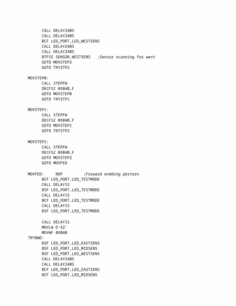
3.2 Software Programming of the microcontrollerThe Source program for PIC16F873A Microcontroller;*************************************************************; Filename:gesanewtonsolartracker.asm ; Date: 29.06.2013; 5:34:18 pm ; File Version: Pic Ide 8.10 ; Author: Microchip Mplab*; Company: Microchip Incorporation *; **************************************************************; Notes: ; 1.80 DEGREE PER STEP

* 0.90 DEGREE PER HALF STEP; 2.49 HIGHER REFERENCE VOLTAGE FOR CONTROLLER* 1.83 LOWER REFERENCE VOLTAGE FOR CONTROLLER; ;*************************************************************
list p=16f873a ; list directive to define processor #include <p16f873a.inc> ; processor specific variable definitions errorlevel -302 ; Turn off banking message __CONFIG _CP_OFF & _WDT_OFF & _BODEN_OFF & _PWRTE_ON & _HS_OSC & _WRT_OFF & _LVP_ON & _CPD_OFF;*****************************************************;Port defintion begins here;*********************************************************;-----------PortASWITCH Equ PORTAPOWER_SW Equ 0x00;TEST_SW Equ 0x01SENSOR Equ PORTAEASTSENS Equ 0x02MIDSENS Equ 0x03WESTSENS Equ 0x04;-----------PortBMOTOR_PORT Equ PORTB;-----------PortCLED_PORT PORTCLED_POWER Equ 0x00;LED_NORMODE Equ 0x01LED_TESTMODE Equ 0x02LED_EASTSENS Equ 0x03LED_MIDSENS Equ 0x04LED_WESTSENS Equ 0x05LED_MOTORACT Equ 0x06;****************************************************
cblock 0x20 ;start of general purpose registersendccblock 0x70 ;start of multi bank general purpose registersw_temp status_temppclath_tempendc
;*************************************************************;RESET_VECTOR
ORG 0x0000 ; processor reset vector
goto start ; go to beginning of program
;************************************************************;INT_VECTOR
ORG 0x0004 ; interrupt vector location
INTERRUPT movwf w_temp ; save off current W register contents movf STATUS,w ; move status register into W register movwf status_temp ; save off contents of STATUS register movf PCLATH,w ; move pclath register into w register

movwf pclath_temp ; save off contents of PCLATH register; isr code can go here or be located as a call subroutine elsewhere movf pclath_temp,w ; retrieve copy of PCLATH register movwf PCLATH ; restore pre-isr PCLATH register contents movf status_temp,w ; retrieve copy of STATUS register movwf STATUS ; restore pre-isr STATUS register contents swapf w_temp,f swapf w_temp,w ; restore pre-isr W register contents retfie ; return from interrupt
;*********************************************MAIN_PROG start;---------------------------------------;Port configuration begins;---------------------------------------
BCF STATUS,RP0BCF STATUS,RP1 ;Bank 0CLRF PORTA ;Initialize all PORTS byCLRF PORTB ;clearing outputCLRF PORTC ;data latches
BSF STATUS,RP0 ;Bank 1MOVLW 0x06 ;Configure all pinsMOVWF ADCON1MOVLW 0xFF ;Configure all pins on port AMOVWF TRISA ;as digital inputsMOVLW 0x68 ;Configure all pins on port BMOVWF TRISB ;as digital outputsMOVLW 0x00 ;Configure all pins on port CMOVWF TRISC ;as digital outputs
;----------------------------------------;initialising ports;---------------------------------------
BCF STATUS,RP0 ;Return to Bank 0;Initialise the stepper motor
BCF MOTOR_PORT,0BCF MOTOR_PORT,1BCF MOTOR_PORT,2BCF MOTOR_PORT,4
CLRF LED_PORT;---------------------------------------;power switch scan start ;---------------------------------------POWSW: BTFSS SWITCH, POWER_SW
GOTO POWONGOTO POWSW
;----------------------------------;system on and start switch scan for test and normal operationPOWON: BSF LED_PORT, LED_POWER ;Put on led reo
CALL DELAY1SCALL DELAY1S
;------------------------------------SWSCAN: BTFSS SWITCH,TEST_SW ;switch scan for test GOTO TESTP

BTFSS SWITCH,POWER_SW ;switch scan for NOR OPERATION GOTO OPEPR
BSF LED_PORT,LED_NORMODECALL DELAY240SBSF LED_PORT,LED_TESTMODECALL DELAY240SBCF LED_PORT,LED_TESTMODECALL DELAY240SBCF LED_PORT,LED_NORMODECALL DELAY240S
GOTO SWSCAN;----------------------------------------;Normal operation begins here;---------------------------------------OPEPR: BSF LED_PORT,LED_NORMODE;;Searching for active sensorSENS_SCAN1:
BTFSC SENSOR,EASTSENSGOTO STOP_SCAN1BTFSC SENSOR,MIDSENSGOTO STOP_SCAN1BTFSC SENSOR,WESTSENSGOTO STOP_SCAN1;CALL MOVE_WWARDGOTO SENS_SCAN1
;-------------STOP_SCAN1:
BTFSS PORTB,6GOTO SENS_SCAN2CALL STEPFWGOTO SENS_SCAN1
;-----------------------------------------SENS_SCAN2:
BTFSC SENSOR,EASTSENSGOTO STOP_SCAN2BTFSC SENSOR,MIDSENSGOTO STOP_SCAN2BTFSC SENSOR,WESTSENSGOTO STOP_SCAN2;CALL MOVE_EWARDGOTO SENS_SCAN2
;-------------STOP_SCAN2:
BTFSS PORTB,5GOTO STOP_SCANCALL STEPBWGOTO SENS_SCAN2
;---------------------------------STOP_SCAN:
BTFSC SENSOR,EASTSENSGOTO STOP_SCAN BTFSC SENSOR,MIDSENSGOTO STOP_SCAN BTFSC SENSOR,WESTSENSGOTO STOP_SCAN

GOTO STOP_SCAN1;-------------------------;MOVE_WWARD:
BTFSS PORTB,6GOTO NIGHT_TIMECALL STEPFWCALL DELAY4MRETURN
NIGHT_TIME:CALL DELAY90MRETURN
;-------------------------;MOVE_EWARD:
BTFSS PORTB,5RETURN CALL STEPBWCALL DELAY4MRETURN
;---------------------------------------;Testing subroutine start here;---------------------------------------TESTP:;------------------------------------;Initialize tray
BTFSS PORTB,5GOTO INIT_OVERCALL STEPBWGOTO TESTP
INIT_OVER:BSF LED_PORT,LED_TESTMODECALL DELAY1SBCF LED_PORT,LED_TESTMODECALL DELAY1SBSF LED_PORT,LED_TESTMODECALL DELAY1SBCF LED_PORT,LED_TESTMODECALL DELAY1SBSF LED_PORT,LED_TESTMODECALL DELAY240S
TRYSTP0:MOVLW D'14'MOVWF 0X040BSF LED_PORT,LED_EASTSENSBCF LED_PORT,LED_MIDSENSBCF LED_PORT,LED_WESTSENSCALL DELAY240SCALL DELAY240SBCF LED_PORT,LED_EASTSENSCALL DELAY240SCALL DELAY240SBTFSS SENSOR,EASTSENS ;Sensor scanning for east GOTO MOVSTEP0GOTO TRYSTP0
TRYSTP1:MOVLW D'14'

MOVWF 0X040BCF LED_PORT,LED_EASTSENSBSF LED_PORT,LED_MIDSENSBCF LED_PORT,LED_WESTSENSCALL DELAY240SCALL DELAY240SBCF LED_PORT,LED_MIDSENSCALL DELAY240SCALL DELAY240SBTFSS SENSOR,MIDSENS ;Sensor scanning for middGOTO MOVSTEP1GOTO TRYSTP1
TRYSTP2: MOVLW D'14'MOVWF 0X040BCF LED_PORT,LED_EASTSENSBCF LED_PORT,LED_MIDSENSBSF LED_PORT,LED_WESTSENSCALL DELAY240SCALL DELAY240SBCF LED_PORT,LED_WESTSENSCALL DELAY240SCALL DELAY240SBTFSS SENSOR,WESTSENS ;Sensor scanning for westGOTO MOVSTEP2GOTO TRYSTP2
MOVSTEP0: CALL STEPFWDECFSZ 0X040,FGOTO MOVSTEP0GOTO TRYSTP1
MOVSTEP1:CALL STEPFWDECFSZ 0X040,FGOTO MOVSTEP1GOTO TRYSTP2
MOVSTEP2:CALL STEPFWDECFSZ 0X040,FGOTO MOVSTEP2GOTO MOVFED
MOVFED: NOP ;Forward endding perternBCF LED_PORT,LED_TESTMODECALL DELAY1SBSF LED_PORT,LED_TESTMODECALL DELAY1SBCF LED_PORT,LED_TESTMODECALL DELAY1SBSF LED_PORT,LED_TESTMODE
CALL DELAY1SMOVLW D'42'

MOVWF 0X040TRYBWD:
BSF LED_PORT,LED_EASTSENSBSF LED_PORT,LED_MIDSENSBSF LED_PORT,LED_WESTSENSCALL DELAY240SCALL DELAY240SBCF LED_PORT,LED_EASTSENSBCF LED_PORT,LED_MIDSENSBCF LED_PORT,LED_WESTSENSCALL DELAY240SCALL DELAY240SBTFSS SENSOR,EASTSENS ;Sensor scanning for east GOTO MOVSTEPBBTFSS SENSOR,MIDSENS ;Sensor scanning for middGOTO MOVSTEPBBTFSS SENSOR,WESTSENS ;Sensor scanning for westGOTO MOVSTEPBGOTO TRYBWD
MOVSTEPB: NOPCALL STEPBWDECFSZ 0X040,FGOTO MOVSTEPBCALL DELAY1S
;Ending testing routinesBCF LED_PORT,LED_TESTMODECALL DELAY1SBSF LED_PORT,LED_TESTMODECALL DELAY1SBCF LED_PORT,LED_TESTMODECALL DELAY1SBSF LED_PORT,LED_TESTMODECALL DELAY240SNOPBCF LED_PORT,LED_EASTSENSBCF LED_PORT,LED_MIDSENSBCF LED_PORT,LED_WESTSENSBCF LED_PORT,LED_TESTMODE
GOTO SWSCAN;----------------------------------------;Stepping motor routine;----------------------------------------STEPBW: BSF LED_PORT,LED_MOTORACT
;MOVLW 0x10 ;MOVWF MOTOR_PORT
BSF MOTOR_PORT,4BCF MOTOR_PORT,0BCF MOTOR_PORT,1BCF MOTOR_PORT,2
CALL DELAY1S;MOVLW 0x04
;MOVWF MOTOR_PORTBSF MOTOR_PORT,2BCF MOTOR_PORT,0

BCF MOTOR_PORT,1BCF MOTOR_PORT,4
CALL DELAY1S;MOVLW 0x02
;MOVWF MOTOR_PORTBSF MOTOR_PORT,1BCF MOTOR_PORT,0BCF MOTOR_PORT,2BCF MOTOR_PORT,4
CALL DELAY1S;MOVLW 0x01
;MOVWF MOTOR_PORTBSF MOTOR_PORT,0BCF MOTOR_PORT,1BCF MOTOR_PORT,2BCF MOTOR_PORT,4
CALL DELAY1SBCF LED_PORT,LED_MOTORACTRETURN
;-------------STEPFW: BSF LED_PORT,LED_MOTORACT
BSF MOTOR_PORT,0BCF MOTOR_PORT,1BCF MOTOR_PORT,2BCF MOTOR_PORT,4
CALL DELAY1SBSF MOTOR_PORT,1BCF MOTOR_PORT,0BCF MOTOR_PORT,2BCF MOTOR_PORT,4
CALL DELAY1SBSF MOTOR_PORT,2BCF MOTOR_PORT,1BCF MOTOR_PORT,2BCF MOTOR_PORT,4
CALL DELAY1SBSF MOTOR_PORT,4BCF MOTOR_PORT,0BCF MOTOR_PORT,1BCF MOTOR_PORT,2
CALL DELAY1SBCF LED_PORT,LED_MOTORACTRETURN
;---------------------------------------;TIMER ROUTINES;---------------------------------------DELAY1MS:
MOVLW 0XFA ;1 sec delay, d'240'MOVWF 0X060
LOOP1: NOPDECFSZ 0X060,FGOTO LOOP1RETURN
DELAY240S: ;240 sec delayMOVLW 0XFA ;d'240'MOVWF 0X061
LOOP2: CALL DELAY1MS

DECFSZ 0X061,FGOTO LOOP2RETURN
DELAY1S: ;1 sec delayMOVLW 0X4 ; d'4'MOVWF 0X062
LOOP3: CALL DELAY240SDECFSZ 0X062,FGOTO LOOP3RETURN
DELAY1M: ;1 min delayMOVLW 0XF0 ;d'240'MOVWF 0X063
LOOP4: CALL DELAY240SDECFSZ 0X063,FGOTO LOOP4RETURN
DELAY4M: MOVLW 0X04MOVWF 0X064
LOOP5: CALL DELAY1MDECFSZ 0X064,FGOTO LOOP5RETURN
DELAY90M:MOVLW 0X5AMOVWF 0X065
LOOP6: CALL DELAY1MDECFSZ 0X065,FGOTO LOOP6RETURN
;-----------------------------;End of processing;-----------------------------
END ; directive 'end of program'
4.0 RESULTS
Measurement of Microcontroller digital outputs was taken every four minutes using
analogue-to-digital Multi-meter. The result is presented Table 3 complied with the switching
period specified in the algorithm of the embedded program.
Table 3 Compared Digital Input/output of the Controller
Comparator/CCP
Input East Sensor 1 Middle Sensor 2 West Sensor 3
Outpu
t
Outpu
1 0 0
0 1 0
0 0 1

t
Outpu
t
Outpu
t
0 0 0
5.0 Discussion
Table 3 shows the Microcontroller’s input and output digital signals for the three
comparators coupled to the East, Middle and West sensors respectively. The value of ‘1’
means ‘ON’ while ‘0’ means ‘OFF’. The null output (0, 0, 0) in Table 3 denote the reset
point at dark hour or zero luminance intensity when the resistance of each sensor
becomes large and the sensors do not conduct. However, an output like (0, 1, 0) implies
that the resistance of the middle sensor is least (its voltage output is highest) compare to
the east and west directional sensors. Therefore when this compared signal value is
coupled to the desired input transistors of the step motor, it tracks the payload to the
central position since that corresponds to the position of maximum photo intensity.
APPENDIX A1: Pin Configuration of PIC16F873A
Pin Name Pin No. Description ApplicationMCLR 1 Reset Input Clears the Memory when in
sleep mode
VDD 20 Positive Supply (+5V) Power Supply to Chip
Vss 8,19 Ground Reference Ground Reference
OSC1 9 For Oscillator Connected to oscillator 4MHz with 10pF
OSC2 10 For oscillator oscillator 4MHz with 10pF
RA0 2 Input/Output Pin Input of Vout from LM324 as speed counter
RB3 24 Input/Output Pin Output to control CW/CCW
of the motor
RB4 25 Input/Output Pin Output to control CW/CCW of the motor
RB1 22 Control pin control the phases of the stepper motor
CCP2 4 Capture/Compare/PMW Output of Duty Cycle to control motor speed
APPENDIX A2: Photograph of the implemented PIC16F873A Microcontroller IC
REFERENCES
1. Crisp, J. (2004). Introduction to Microprocessors and Microcontrollers. Second Edition.
Jordan Hill: Oxford.
2. Kularatna, N. (2000). Modern Component Families and Circuit Block Design.
Butterworth-Heinemann, Woburn, MA: USA.
3. Microchip (2006). MPLAB IDE User’s Guide: Microchip Technology Inc.
4. Microchip (2010). PIC16F87XA Datasheet: www.Microchip.com
5. Microchip (2010). PIC Mid-Range Reference Manual: Microchip Technology Inc.

6. O’Neil, R. D. Lewis, L.; Lim, C. P; and Harmsen J. (2002) Laboratory Introduction to
Embedded Control, lab manual version 9.4. New York: RPI.
7. Saxena, A. K. and Dutta, V. (1990). A versatile Microprocessor Based Controller for
Solar Tracking. Proc. IEEE, pp. 1105 – 1109.
8. Sedra, A. S. and Smith, K. C. (2004). Microelectronics Circuits. Volume 1 Oxford
University Press: New York.
9. Thommandru, Y. (2006). Programming a PIC Microcontroller- A Short Tutorial: Iowa
State University.


