yuezhangee494.weebly.comyuezhangee494.weebly.com/uploads/1/5/3… · Web view · 2013-03-12EE330...
8
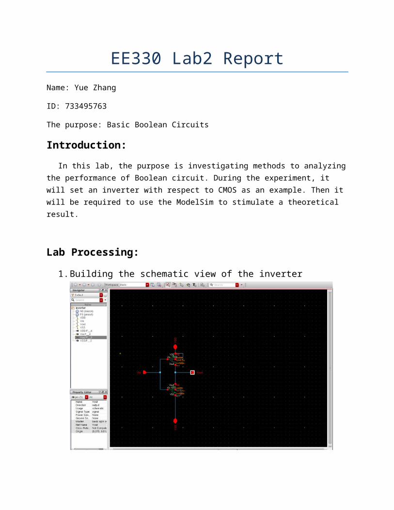
EE330 Lab2 Report Name: Yue Zhang ID: 733495763 The purpose: Basic Boolean Circuits Introduction: In this lab, the purpose is investigating methods to analyzing the performance of Boolean circuit. During the experiment, it will set an inverter with respect to CMOS as an example. Then it will be required to use the ModelSim to stimulate a theoretical result. Lab Processing: 1. Building the schematic view of the inverter
Transcript of yuezhangee494.weebly.comyuezhangee494.weebly.com/uploads/1/5/3… · Web view · 2013-03-12EE330...
EE330 Lab2 ReportName: Yue Zhang
ID: 733495763
The purpose: Basic Boolean Circuits
Introduction:
In this lab, the purpose is investigating methods to analyzing the performance of Boolean circuit. During the experiment, it will set an inverter with respect to CMOS as an example. Then it will be required to use the ModelSim to stimulate a theoretical result.
Lab Processing:
1. Building the schematic view of the inverter
M1: Wight=1.5u, Length=0.6uM2: Wight=4.5u, Length=0.6u

2. Making the test circuit for the invertera) Create a inverter symbol and contact the circuit:
b) Inverter transient response simulation:
In the plot, because the function of inverter is to invert a converse value in term of input value, Vout gets a low value with respect to high Vin, a high Vout as regard to low Vin.

c) Inverter transfer characteristics simulation:
In the plot, at beginning, the pink line is Vin that changes point is about Vin=0.8V, and the blue line is Vout that changes voltage is about 4.99V. the intersection point is V=2.72V. At the end the change voltage of Vin is about 4.2V, and changes voltage of Vout is about 0.02V.
3. Inverter driving a load
1pf
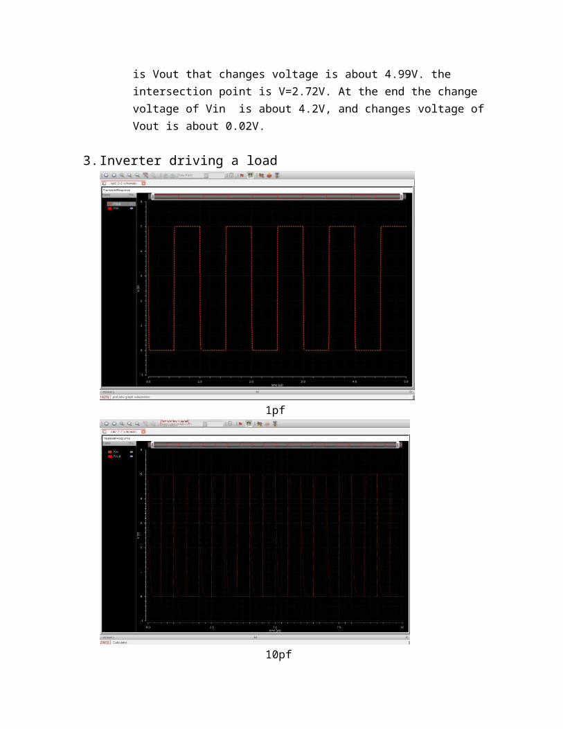
10pf
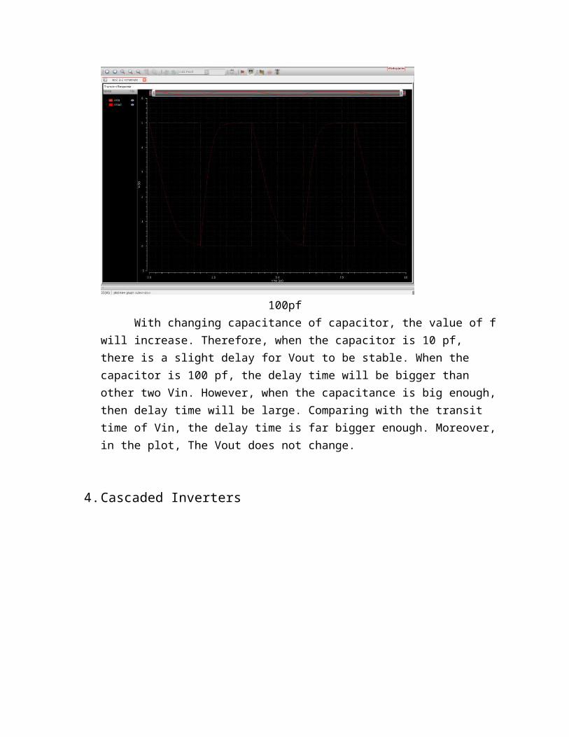
100pfWith changing capacitance of capacitor, the value of f will increase. Therefore,
when the capacitor is 10 pf, there is a slight delay for Vout to be stable. When the capacitor is 100 pf, the delay time will be bigger than other two Vin. However, when the capacitance is big enough, then delay time will be large. Comparing with the transit time of Vin, the delay time is far bigger enough. Moreover, in the plot, The Vout does not change.
4. Cascaded Inverters
Since in the cascaded inverter, it has two inverters, therefore the result of Vout2 should be equal to Vin.

5. Inverter Simulation with Verilog HDL by ModelSima. timescale 1ns/1ps
module inverter(Vout,Vdd,Vvss,Vin);input Vin;input Vdd;input Vss;output Vout;
wire Vout;assign Vout = ~Vin;endmodule
b. `timescale 1ns/1psmodule testbench;
reg Vin;reg Vss;reg Vdd;
inverter IN_1(Vin(Vin),.Vss(Vss),. Vdd(Vdd),.Vout(Vout));initial begin
Vin=1;endendmoduleThe result wave is:
Conclusion:
In this lab, I learn how to use investigating methods to analyzing the performance of Boolean circuit. Then I know use the ModelSim to stimulate a theoretical result.