WB_MEM_CTRL Configurable Wishbone Memory Controller
33
WB_MEM_CTRL Configurable Wishbone Memory Controller Summary Core Reference CR0152 (v2.1) October 10, 2007 This document provides detailed reference information with respect to the configurable memory controller peripheral device. The WB_MEM_CTRL is a Wishbone-compliant configurable memory controller that, depending on its configuration, provides a simple interface between a 32-bit processor and either single data rate Synchronous DRAM, Asynchronous Static RAM, 32-bit wide Block RAM (single or dual port), or parallel Flash memory. If you need to access common-bus memory on a 3-connector daughter board, you need to use the WB_SHARED_MEM_CTRL peripheral. For more information on this device, refer to the document CR0176 WB_SHARED_MEM_CTRL Configurable Shared Memory Controller. Features • Simplified connection to processor’s External Memory interface via a Wishbone Interconnect • Completely configurable from the schematic sheet • Configurable as either SRAM, SDRAM, or BRAM Controller - SDRAM Controller – interfaces to 8-, 16, or 32-bit wide SDR SDRAM - SRAM Controller – interfaces to 8-, 16, or 32-bit wide asynchronous SRAM - BRAM Controller – interfaces to 32-bit wide single or dual port Block RAM - Flash Controller – interfaces to 8-, 16, or 32-bit wide parallel Flash memory • Automatic sizing of ADR_I input bus, based on specified physical memory size • Wishbone-compliant. Available devices The WB_MEM_CTRL device can be found in the FPGA Peripherals integrated library (\Program Files\Altium Designer 6\Library\Fpga\FPGA Peripherals.IntLib). CR0152 (v2.1) October 10, 2007 1
-
Upload
flashdomain -
Category
Documents
-
view
456 -
download
1
Transcript of WB_MEM_CTRL Configurable Wishbone Memory Controller

WB_MEM_CTRL Configurable Wishbone Memory Controller
Summary Core Reference CR0152 (v2.1) October 10, 2007
This document provides detailed reference information with respect to the configurable memory controller peripheral device.
The WB_MEM_CTRL is a Wishbone-compliant configurable memory controller that, depending on its configuration, provides a simple interface between a 32-bit processor and either single data rate Synchronous DRAM, Asynchronous Static RAM, 32-bit wide Block RAM (single or dual port), or parallel Flash memory.
If you need to access common-bus memory on a 3-connector daughter board, you need to use the WB_SHARED_MEM_CTRL peripheral. For more information on this device, refer to the document CR0176 WB_SHARED_MEM_CTRL Configurable Shared Memory Controller.
Features • Simplified connection to processor’s External Memory interface via a Wishbone Interconnect
• Completely configurable from the schematic sheet
• Configurable as either SRAM, SDRAM, or BRAM Controller
- SDRAM Controller – interfaces to 8-, 16, or 32-bit wide SDR SDRAM
- SRAM Controller – interfaces to 8-, 16, or 32-bit wide asynchronous SRAM
- BRAM Controller – interfaces to 32-bit wide single or dual port Block RAM
- Flash Controller – interfaces to 8-, 16, or 32-bit wide parallel Flash memory
• Automatic sizing of ADR_I input bus, based on specified physical memory size
• Wishbone-compliant.
Available devices The WB_MEM_CTRL device can be found in the FPGA Peripherals integrated library (\Program Files\Altium Designer 6\Library\Fpga\FPGA Peripherals.IntLib).
CR0152 (v2.1) October 10, 2007 1

WB_MEM_CTRL Configurable Wishbone Memory Controller
Functional description
WB_MEM_CTRL configured as SDRAM Controller
Symbol
Figure 1. WB_MEM_CTRL symbol (Configured as SDRAM Controller)
Figure 1 shows the five possible schematic symbol representations for the Memory Controller device, when configured to operate as an SDRAM Controller. The SDRAM interface pinout is determined by the specified Memory Layout, when configuring the Memory Controller. The symbols in Figure 1 reflect the following layouts:
• Top Left – 1 x 8-bit Wide Device
• Bottom Left – 2 x 8-bit Wide Devices
2 CR0152 (v2.1) October 10, 2007

WB_MEM_CTRL Configurable Wishbone Memory Controller
• Top Center – 1 x 16-bit Wide Device
• Bottom Center – 2 x 16-bit Wide Devices
• Right – 1 x 32-bit Wide Device. Note: The symbols shown in Figure 1 represent the Memory Controller when configured to connect to physical SDRAM that is 16MB (4M x 32-bit) in size. Depending on the size of SDRAM that you specify the Controller to work with, the ADR_I signal will change in size accordingly.
Pin description Table 1. WB_MEM_CTRL Pin description (SDRAM-configured)
Name Type Polarity/ Bus size
Description
Control Signals
CLK_I I Rise External (system) clock signal
RST_I I High External (system) reset signal
Host Processor Interface Signals
STB_I I High Strobe signal. When asserted, indicates the start of a valid Wishbone data transfer cycle
CYC_I I High Cycle signal. When asserted, indicates the start of a valid Wishbone bus cycle. This signal remains asserted until the end of the bus cycle, where such a cycle can include multiple data transfers
ACK_O O High Standard Wishbone device acknowledgement signal. When this signal goes High, the Memory Controller (Wishbone Slave) has finished execution of the requested action and the current bus cycle is terminated
ADR_I I 23-271 Standard Wishbone address bus. Used to select an address in the connected BRAM for writing to/reading from
DAT_O O 32 Data to be sent to the connected Wishbone master device
DAT_I I 32 Data received from the connected Wishbone master device
SEL_I I 4/High Select input, used to determine where data is placed on the DAT_O line during a Read cycle and from where on the DAT_I line data is accessed during a Write cycle. Each of the data ports is 32-bits wide with 8-bit granularity, meaning data transfers can be 8-, 16- or 32-bit. The four select bits
1 Depends on the size of physical SDRAM connected to (see Table 5).
CR0152 (v2.1) October 10, 2007 3

WB_MEM_CTRL Configurable Wishbone Memory Controller
Name Type Polarity/ Bus size
Description
allow targeting of each of the four active bytes of a port, with bit 0 corresponding to the low byte (7..0) and bit 3 corresponding to the high byte (31..24)
WE_I I Level Write enable signal. Used to indicate whether the current local bus cycle is a Read or Write cycle.
0 = Read
1 = Write
SDRAM Interface Signals
SDRAM_D IO 8/16/32 Memory Data Bus
SDRAM_A O 13 Memory Address Bus. This bus provides values used to select the row (SDRAM_RAS = 0, SDRAM_CAS=1) and column (SDRAM_RAS=1, SDRAM_CAS=0). The latter determines the address in the memory array from where to read (SDRAM_WE=0) or write (SDRAM_WE=1).
SDRAM_BA O 2 Memory Bank Address
SDRAM_BE O 4/Low Byte Enable signal. This signal is equivalent to SEL_I, but with the polarity reversed
SDRAM_RAS O Low Row Address Select. When this signal is taken Low, the value on the SDRAM_A bus is used to select the bank and activate the required row.
SDRAM_CAS O Low Column Address Select. When taken Low, the value on the SDRAM_A bus is used to select the bank and required column. A Read or Write will then be conducted from that memory location, depending on the state of SDRAM_WE.
SDRAM_WE O Level Memory Write Enable. Determines whether the location in memory addressed by SDRAM_A is written to or read from:
0 = Read
1 = Write
SDRAM_CS O Low Memory Chip Select
SDRAM_CLK I High SDRAM Clock signal. The frequency of the clock signal must be the same as the speed of the memory. If the SDRAM is PC100 (100MHz), then a 100MHz clock signal must be made available within the FPGA to this input.
SDRAM_CLKE O High Clock Enable
4 CR0152 (v2.1) October 10, 2007
WB_MEM_CTRL Configurable Wishbone Memory Controller
WB_MEM_CTRL configured as SRAM Controller
Symbols
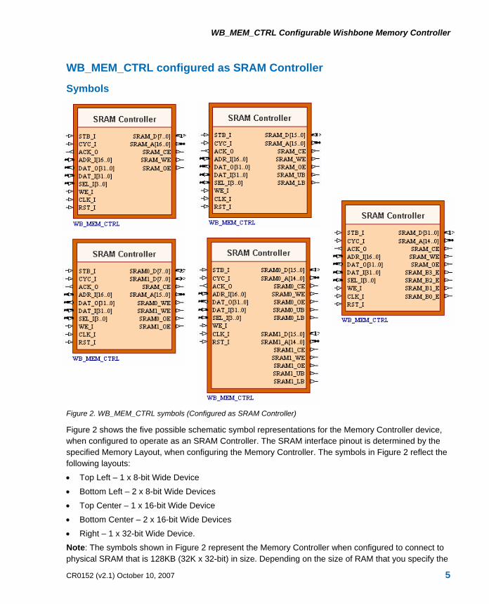
Figure 2. WB_MEM_CTRL symbols (Configured as SRAM Controller)
Figure 2 shows the five possible schematic symbol representations for the Memory Controller device, when configured to operate as an SRAM Controller. The SRAM interface pinout is determined by the specified Memory Layout, when configuring the Memory Controller. The symbols in Figure 2 reflect the following layouts:
• Top Left – 1 x 8-bit Wide Device
• Bottom Left – 2 x 8-bit Wide Devices
• Top Center – 1 x 16-bit Wide Device
• Bottom Center – 2 x 16-bit Wide Devices
• Right – 1 x 32-bit Wide Device. Note: The symbols shown in Figure 2 represent the Memory Controller when configured to connect to physical SRAM that is 128KB (32K x 32-bit) in size. Depending on the size of RAM that you specify the
CR0152 (v2.1) October 10, 2007 5
WB_MEM_CTRL Configurable Wishbone Memory Controller
Controller to work with, the SRAM_A (SRAM0_A, SRAM1_A) and ADR_I signals will change in size accordingly.
Pin description Table 2. WB_MEM_CTRL Pin description (SRAM-configured)
Name Type Polarity/Bus size
Description
Control Signals
CLK_I I Rise External (system) clock signal
RST_I I High External (system) reset signal
Host Processor Interface Signals
STB_I I High Strobe signal. When asserted, indicates the start of a valid Wishbone data transfer cycle
CYC_I I High Cycle signal. When asserted, indicates the start of a valid Wishbone bus cycle. This signal remains asserted until the end of the bus cycle, where such a cycle can include multiple data transfers
ACK_O O High Standard Wishbone device acknowledgement signal. When this signal goes High, the Memory Controller (Wishbone Slave) has finished execution of the requested action and the current bus cycle is terminated
ADR_I I 10-242 Standard Wishbone address bus. Used to select an address in the connected SRAM for writing to/reading from
DAT_O O 32 Data to be sent to the connected Wishbone master device
DAT_I I 32 Data received from the connected Wishbone master device
SEL_I I 4/High Select input, used to determine where data is placed on the DAT_O line during a Read cycle and from where on the DAT_I line data is accessed during a Write cycle. Each of the data ports is 32-bits wide with 8-bit granularity, meaning data transfers can be 8-, 16- or 32-bit. The four select bits allow targeting of each of the four active bytes of a port, with bit 0 corresponding to the low byte (7..0) and bit 3 corresponding to the high byte (31..24)
WE_I I Level Write enable signal. Used to indicate whether the current local bus cycle is a Read or Write cycle.
2 Depends on the size of physical RAM connected to (see Table 6).
6 CR0152 (v2.1) October 10, 2007

WB_MEM_CTRL Configurable Wishbone Memory Controller
Name Type Polarity/Bus size
Description
0 = Read
1 = Write
SRAM Interface Signals
SRAM_D IO 8/16/32 Memory Data Bus
SRAM_A O 8-243 Memory Address Bus
SRAM_CE O Low Memory Chip Enable
SRAM_WE O Low Memory Write Enable – active when performing a write to an addressed location in memory
SRAM_OE O Low Memory Output Enable – active when performing a read from an addressed location in memory
SRAM_UB4 O Low Upper Byte Select
SRAM_LB O Low Lower Byte Select
SRAM_B3_E5 O Low Byte 3 Select
SRAM_B2_E5 O Low Byte 2 Select
SRAM_B1_E5 O Low Byte 1 Select
SRAM_B0_E5 O Low Byte 0 Select
3 Depends on the size of physical RAM connected to (see Table 6) 4 1 x 16-bit and 2 x 16-bit devices only. 5 1 x 32-bit device only.
CR0152 (v2.1) October 10, 2007 7

WB_MEM_CTRL Configurable Wishbone Memory Controller
WB_MEM_CTRL configured as BRAM Controller
Symbol
Figure 3. WB_MEM_CTRL symbol (Configured as BRAM Controller)
Note: The symbol shown in Figure 3 represents the Memory Controller when configured to connect to physical Block RAM that is 16KB (4K x 32-bit) in size. Depending on the size of RAM that you specify the Controller to work with, the BRAM_A and ADR_I signals will change in size accordingly.
Pin description Table 3. WB_MEM_CTRL Pin description (BRAM-configured)
Name Type Polarity/ Bus size
Description
Control Signals
CLK_I I Rise External (system) clock signal
RST_I I High External (system) reset signal
Host Processor Interface Signals
STB_I I High Strobe signal. When asserted, indicates the start of a valid Wishbone data transfer cycle
CYC_I I High Cycle signal. When asserted, indicates the start of a valid Wishbone bus cycle. This signal remains asserted until the end of the bus cycle, where such a cycle can include multiple data transfers
ACK_O O High Standard Wishbone device acknowledgement signal. When this signal goes High, the Memory Controller (Wishbone Slave) has finished execution of the requested action and the current bus cycle is terminated
8 CR0152 (v2.1) October 10, 2007

WB_MEM_CTRL Configurable Wishbone Memory Controller
Name Type Polarity/ Bus size
Description
ADR_I I 10-246 Standard Wishbone address bus. Used to select an address in the connected BRAM for writing to/reading from
DAT_O O 32 Data to be sent to the connected Wishbone master device
DAT_I I 32 Data received from the connected Wishbone master device
SEL_I I 4/High Select input, used to determine where data is placed on the DAT_O line during a Read cycle and from where on the DAT_I line data is accessed during a Write cycle. Each of the data ports is 32-bits wide with 8-bit granularity, meaning data transfers can be 8-, 16- or 32-bit. The four select bits allow targeting of each of the four active bytes of a port, with bit 0 corresponding to the low byte (7..0) and bit 3 corresponding to the high byte (31..24)
WE_I I Level Write enable signal. Used to indicate whether the current local bus cycle is a Read or Write cycle.
0 = Read
1 = Write
BRAM Interface Signals
BRAM_DI O 32 Data to be sent to memory
BRAM_DO I 32 Data received from memory
BRAM_A O 8-226 Memory Address Bus
BRAM_WE O Level Memory Write Enable. Determines whether the location in memory addressed by BRAM_A is written to or read from:
0 = Read
1 = Write
BRAM_EN O High Memory Enable – made active to be able to write to/read from an addressed location in memory
BRAM_BW O 4/High Byte Read/Write signal. This signal is equivalent to, and follows, the SEL_I signal.
6 Depends on the size of physical RAM connected to (see Table 7)
CR0152 (v2.1) October 10, 2007 9

WB_MEM_CTRL Configurable Wishbone Memory Controller
WB_MEM_CTRL configured as Flash Controller
Symbol
Figure 4. WB_MEM_CTRL symbol (Configured as Flash Controller)
Figure 4 shows the five possible schematic symbol representations for the Memory Controller device, when configured to operate as a Flash Controller. The Flash interface pinout is determined by the specified Memory Layout, when configuring the Memory Controller. The symbols in Figure 1 reflect the following layouts:
• Top Left – 1 x 8-bit Wide Device
• Bottom Left – 2 x 8-bit Wide Devices
• Top Center – 1 x 16-bit Wide Device
• Bottom Center – 2 x 16-bit Wide Devices
• Right – 1 x 32-bit Wide Device. Note: The symbols shown in Figure 1 represent the Memory Controller when configured to connect to physical Flash memory that is 64MB (16M x 32-bit) in size. Depending on the size of Flash memory that you specify the Controller to work with, the FLASH_A (FLASH0_A, FLASH1_A) and ADR_I signals will change in size accordingly.
10 CR0152 (v2.1) October 10, 2007

WB_MEM_CTRL Configurable Wishbone Memory Controller
Pin description Table 4. WB_MEM_CTRL Pin description (Flash-configured)
Name Type Polarity/ Bus size
Description
Control Signals
CLK_I I Rise External (system) clock signal
RST_I I High External (system) reset signal
Host Processor Interface Signals
STB_I I High Strobe signal. When asserted, indicates the start of a valid Wishbone data transfer cycle
CYC_I I High Cycle signal. When asserted, indicates the start of a valid Wishbone bus cycle. This signal remains asserted until the end of the bus cycle, where such a cycle can include multiple data transfers
ACK_O O High Standard Wishbone device acknowledgement signal. When this signal goes High, the Memory Controller (Wishbone Slave) has finished execution of the requested action and the current bus cycle is terminated
ADR_I I 10-277 Standard Wishbone address bus. Used to select an address in the connected Flash memory for writing to/reading from
DAT_O O 32 Data to be sent to the connected Wishbone master device
DAT_I I 32 Data received from the connected Wishbone master device
SEL_I I 4/High Select input, used to determine where data is placed on the DAT_O line during a Read cycle and from where on the DAT_I line data is accessed during a Write cycle. Each of the data ports is 32-bits wide with 8-bit granularity, meaning data transfers can be 8-, 16- or 32-bit. The four select bits allow targeting of each of the four active bytes of a port, with bit 0 corresponding to the low byte (7..0) and bit 3 corresponding to the high byte (31..24)
WE_I I Level Write enable signal. Used to indicate whether the current local bus cycle is a Read or Write cycle.
0 = Read
1 = Write
7 Depends on the size of physical Flash memory connected to (see Table 8).
CR0152 (v2.1) October 10, 2007 11

WB_MEM_CTRL Configurable Wishbone Memory Controller
Name Type Polarity/ Bus size
Description
Flash Memory Interface Signals
FLASH_D IO 32 Memory Data Bus
FLASH_A O 8-278 Memory Address Bus
FLASH_CE O Low Memory Chip Enable
FLASH_WE O Low Memory Write Enable. Take this line Low to write to the memory location addressed by FLASH_A
FLASH_OE O Low Memory Output Enable. Take this line Low to read from the memory location addressed by FLASH_A
8 Depends on the size of physical Flash memory connected to (see Table 8).
12 CR0152 (v2.1) October 10, 2007

WB_MEM_CTRL Configurable Wishbone Memory Controller
Configuring the device from the schematic design The WB_MEM_CTRL device can be configured after placement on the schematic sheet using the Configure (Memory Controller) dialog (Figure 5). Access this dialog by right-clicking over the device and choosing the Configure command from the context menu that appears. Alternatively, click on the Configure button, available in the Component Properties dialog for the device.
Figure 5. Configuring the Memory Controller peripheral.
Use the Memory Type region of the dialog to choose the type of memory that you wish to interface to. Choose from either:
• Synchronous DRAM
• Asynchronous SRAM
• Block RAM, or
• Parallel FLASH.
The configuration options presented in the dialog will change in accordance with your selection.
SDRAM Controller configuration When the chosen memory type is Synchronous DRAM, the Configure (Memory Controller) dialog will appear as shown in Figure 6.
CR0152 (v2.1) October 10, 2007 13

WB_MEM_CTRL Configurable Wishbone Memory Controller
Figure 6. Configuration options when interfacing to SDRAM.
The following sections detail each of the configuration options available.
Size of SDRAM memory Use this region to specify the size of the physical SDRAM that you are interfacing to. The width of the ADR_I input line will automatically change in accordance with the memory size specified.
Table 5 lists the supported SDRAM sizes and the corresponding size of the Wishbone address bus (ADR_I) for each configuration of the Memory Controller.
Table 5. SDRAM size selection and effect on address size.
Wishbone Address Bus (ADR_I) sizing for each Memory Layout SDRAM Size
1 x 8-bit 2 x 8-bit 1 x 16-bit 2 x 16-bit 1 x 32-bit
8MB 23 23 23 X 23
16MB 24 24 24 24 24
32MB X 25 25 25 25
64MB X 26 X 26 26
128MB X X X 27 X
X – Memory Layout not available for chosen SDRAM size.
14 CR0152 (v2.1) October 10, 2007

WB_MEM_CTRL Configurable Wishbone Memory Controller
Memory Layout Use the drop-down in this region of the dialog to select the layout for the physical memory. The following is a list of all possible layouts:
• 1 x 32-bit Wide Device
• 1 x 16-bit Wide Device
• 1 x 8-bit Wide Device
• 2 x 16-bit Wide Devices
• 2 x 8-bit Wide Devices.
The actual layouts available will depend on the chosen size of SDRAM memory. Refer back to Table 4 to see which layouts are available with which memory sizes.
The schematic symbol for the placed Memory Controller will automatically be updated to reflect your selection, upon leaving the dialog.
In addition to determining the interface pinout for connection to the physical memory device(s), the memory layout also determines the number of accesses required to read or write a single 32-bit word.
Memory Settings Use this region of the dialog to specify the speed of the memory you are working with (in MHz). The frequency of the signal arriving at the Controller's SDRAM_CLK input must equal the value specified for the SDRAM Clock Frequency in MHz.
The Keep Current Row Open option allows you to keep the current row open – essentially disabling the SDRAM device's auto-precharge feature, which otherwise causes a precharge of the addressed bank/row upon completion of the current Read or Write. This enables faster memory access when successively accessing the same row. If this option is set to No, the SDRAM device's auto-precharge feature is enabled and the current row will be closed after each memory access.
Both settings in this region are used to calculate reload values for refresh counters internal to the Controller.
Timer Settings The following timing-related settings can be defined in this region of the dialog, with each setting specified in terms of cycles of the SDRAM_CLK signal. Together, these settings are used to determine memory timing protocols. Write Recovery time (tWR) – the minimum number of clock cycles between registration of the last required data element in a Write access and the start of a subsequent precharge for that row/bank. (Default = 4 cycles). Auto Refresh period (tRFC) – the number of clock cycles required for the SDRAM device to perform one Auto Refresh cycle. (Default = 16 cycles). Active to Read or Write delay (tRCD) – the minimum number of clock cycles that must be observed between the start of an access to memory (a particular row of a bank is opened for access) and the Read or Write actually being performed. (Default = 8 cycles).
CR0152 (v2.1) October 10, 2007 15
WB_MEM_CTRL Configurable Wishbone Memory Controller
Precharge command period (tRP) – the number of clock cycles required to perform a precharge, which is simply the closing of the open row in a specific bank or the open row in all banks. During a precharge, the bank(s) will be idle and no Read or Write access is permitted. (Default = 16 cycles). CAS latency (tCAS) – the delay, in clock cycles, between the SDRAM device registering a Read access and the availability of the first piece of output data. This is typically set to 2 or 3 clock cycles (Default = 2 cycles).
The drop-down field at the bottom of this region allows you to define the synchronization scheme to be used when interfacing to SDRAM. The following three options allow you to specify the relationship between the SDRAM_CLK input – the frequency of which is the same as the speed of memory you are using – and the external system clock, CLK_I – input to the processor and used as the Wishbone clock. • Independent clocks – use this option when the memory is being clocked at a higher speed than
the FPGA design. This option provides flexibility when debugging a design, as you can use any frequency for CLK_I (provided it's lower than SDRAM_CLK). However time is lost, in terms of data throughput, performing a resync between the Wishbone interface and the memory controller.
• Memory clock 2x Wishbone clock – use this option when the memory is being clocked at twice the speed of the FPGA design (e.g. SDRAM running at 100MHz and system clock for the design (CLK_I) is 50MHz). Time is still lost when performing a resync, but the resync is preformed faster due to prior knowledge of the relationship between the clocks. You can slow down the design clock, but this will result in the memory becoming slower too.
• Same clock – use this option when the memory is being clocked at the same speed as the FPGA design. This option is typically for slower FPGA devices, which can not be clocked as high as 100MHz. No resync is required between the Wishbone interface and the memory controller.
Note: Ensure that the frequency of the signal wired to the Controller's SDRAM_CLK input is in accordance with the synchronization setting you have chosen.
16 CR0152 (v2.1) October 10, 2007
WB_MEM_CTRL Configurable Wishbone Memory Controller
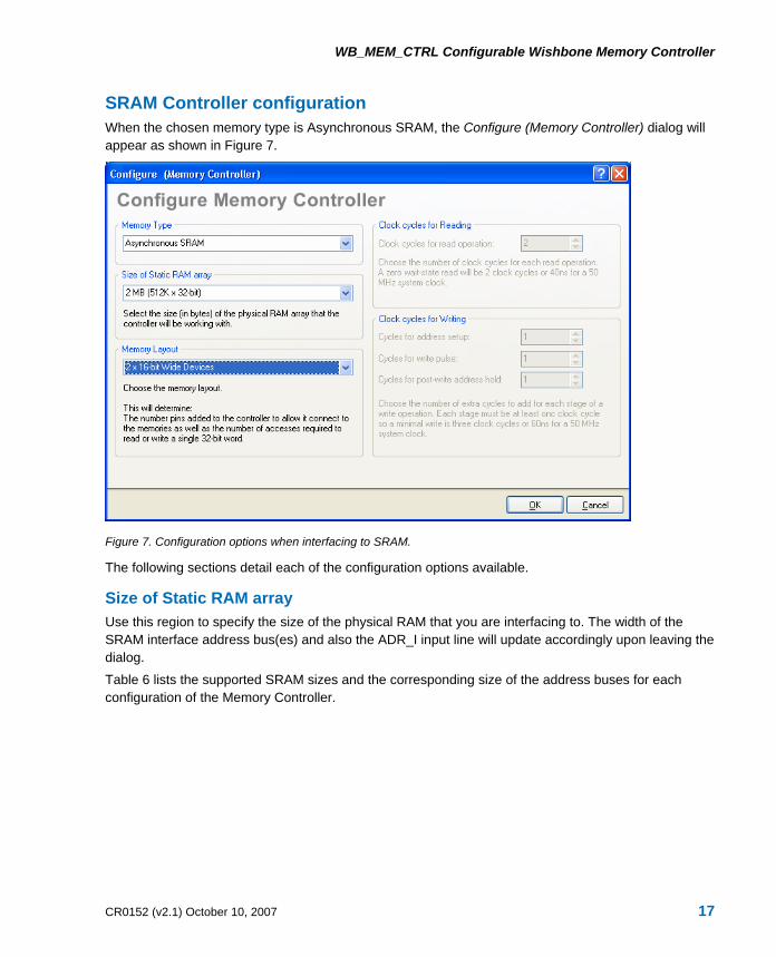
SRAM Controller configuration When the chosen memory type is Asynchronous SRAM, the Configure (Memory Controller) dialog will appear as shown in Figure 7.
Figure 7. Configuration options when interfacing to SRAM.
The following sections detail each of the configuration options available.
Size of Static RAM array Use this region to specify the size of the physical RAM that you are interfacing to. The width of the SRAM interface address bus(es) and also the ADR_I input line will update accordingly upon leaving the dialog.
Table 6 lists the supported SRAM sizes and the corresponding size of the address buses for each configuration of the Memory Controller.
CR0152 (v2.1) October 10, 2007 17

WB_MEM_CTRL Configurable Wishbone Memory Controller
Table 6. SRAM size selection and effect on address size.
Address Bus Sizing for each Memory Layout
1 x 8-bit 2 x 8-bit 1 x 16-bit 2 x 16-bit 1 x 32-bit
SRAM Size
ADR_I SRAM_A ADR_I SRAM_A ADR_I SRAM_A ADR_I SRAM0_A SRAM1_A
ADR_I SRAM_A
1Kb 10 10 10 9 10 9 10 8 10 8
2Kb 11 11 11 10 11 10 11 9 11 9
4Kb 12 12 12 11 12 11 12 10 12 10
8Kb 13 13 13 12 13 12 13 11 13 11
16Kb 14 14 14 13 14 13 14 12 14 12
32Kb 15 15 15 14 15 14 15 13 15 13
64Kb 16 16 16 15 16 15 16 14 16 14
128Kb 17 17 17 16 17 16 17 15 17 15
256Kb 18 18 18 17 18 17 18 16 18 16
512Kb 19 19 19 18 19 18 19 17 19 17
1Mb 20 20 20 19 20 19 20 18 20 18
2Mb 21 21 21 20 21 20 21 19 21 19
4Mb 22 22 22 21 22 21 22 20 22 20
8Mb 23 23 23 22 23 22 23 21 23 21
16Mb 24 24 24 23 24 23 24 22 24 22
Memory Layout Use the drop-down available in this region of the dialog to select the layout for the physical memory:
• 1 x 32-bit Wide Device
• 1 x 16-bit Wide Device
• 1 x 8-bit Wide Device
• 2 x 16-bit Wide Devices
• 2 x 8-bit Wide Devices.
The schematic symbol for the placed Memory Controller will automatically be updated to reflect your selection, upon leaving the dialog.
In addition to determining the interface pinout for connection to the physical memory device(s), the memory layout also determines the number of accesses required to read or write a single 32-bit word.
18 CR0152 (v2.1) October 10, 2007
WB_MEM_CTRL Configurable Wishbone Memory Controller
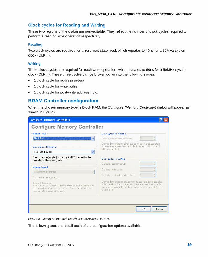
Clock cycles for Reading and Writing These two regions of the dialog are non-editable. They reflect the number of clock cycles required to perform a read or write operation respectively.
Reading Two clock cycles are required for a zero wait-state read, which equates to 40ns for a 50MHz system clock (CLK_I).
Writing Three clock cycles are required for each write operation, which equates to 60ns for a 50MHz system clock (CLK_I). These three cycles can be broken down into the following stages:
• 1 clock cycle for address set-up
• 1 clock cycle for write pulse
• 1 clock cycle for post-write address hold.
BRAM Controller configuration When the chosen memory type is Block RAM, the Configure (Memory Controller) dialog will appear as shown in Figure 8.
Figure 8. Configuration options when interfacing to BRAM.
The following sections detail each of the configuration options available.
CR0152 (v2.1) October 10, 2007 19

WB_MEM_CTRL Configurable Wishbone Memory Controller
Size of Block RAM array Use this region to specify the size of the physical RAM that you are interfacing to. The width of the BRAM interface address bus and also the ADR_I input line will update accordingly upon leaving the dialog.
Table 7 lists the supported BRAM sizes and the corresponding size of the address buses for each configuration of the Memory Controller.
Table 7. BRAM size selection and effect on address size.
Address Bus Sizing RAM Size
ADR_I BRAM_A
1Kb 10 8
2Kb 11 9
4Kb 12 10
8Kb 13 11
16Kb 14 12
32Kb 15 13
64Kb 16 14
128Kb 17 15
256Kb 18 16
512Kb 19 17
1Mb 20 18
2Mb 21 19
4Mb 22 20
8Mb 23 21
16Mb 24 22
Memory Layout This region of the dialog is non-editable and reflects the layout of physical BRAM that can be connected to the Controller – in this case a single 1 x 32-bit wide device.
Clock cycles for Reading and Writing These two regions of the dialog are non-editable. They reflect the number of clock cycles required to perform a read or write operation respectively.
20 CR0152 (v2.1) October 10, 2007

WB_MEM_CTRL Configurable Wishbone Memory Controller
Reading Two clock cycles are required for a zero wait-state read, which equates to 40ns for a 50MHz system clock (CLK_I).
Writing Three clock cycles are required for each write operation, which equates to 60ns for a 50MHz system clock (CLK_I). These three cycles can be broken down into the following stages:
• 1 clock cycle for address set-up
• 1 clock cycle for write pulse
• 1 clock cycle for post-write address hold.
Flash Memory Controller configuration When the chosen memory type is Parallel FLASH, the Configure (Memory Controller) dialog will appear as shown in Figure 9.
Figure 9. Configuration options when interfacing to Flash memory.
The following sections detail each of the configuration options available.
Size of Parallel Flash array Use this region to specify the size of the physical memory that you are interfacing to. The width of the Flash memory interface address bus(es) and also the ADR_I input line will update accordingly upon leaving the dialog. Table 8 lists the supported Flash memory sizes and the corresponding size of the address buses for each configuration of the Memory Controller.
CR0152 (v2.1) October 10, 2007 21

WB_MEM_CTRL Configurable Wishbone Memory Controller
Table 8. Flash memory size selection and effect on address size.
Address Bus Sizing for each Memory Layout
1 x 8-bit 2 x 8-bit 1 x 16-bit 2 x 16-bit 1 x 32-bit
Flash Size
ADR_I FLASH_A ADR_I FLASH_A ADR_I FLASH_A ADR_I FLASH0_A FLASH1_A
ADR_I FLASH_A
1Kb 10 10 10 9 10 9 10 8 10 8
2Kb 11 11 11 10 11 10 11 9 11 9
4Kb 12 12 12 11 12 11 12 10 12 10
8Kb 13 13 13 12 13 12 13 11 13 11
16Kb 14 14 14 13 14 13 14 12 14 12
32Kb 15 15 15 14 15 14 15 13 15 13
64Kb 16 16 16 15 16 15 16 14 16 14
128Kb 17 17 17 16 17 16 17 15 17 15
256Kb 18 18 18 17 18 17 18 16 18 16
512Kb 19 19 19 18 19 18 19 17 19 17
1Mb 20 20 20 19 20 19 20 18 20 18
2Mb 21 21 21 20 21 20 21 19 21 19
4Mb 22 22 22 21 22 21 22 20 22 20
8Mb 23 23 23 22 23 22 23 21 23 21
16Mb 24 24 24 23 24 23 24 22 24 22
32Mb 25 25 25 24 25 24 25 23 25 23
64Mb 26 26 26 25 26 25 26 24 26 24
128Mb 27 27 27 26 27 26 27 25 27 25
Memory Layout Use the drop-down available in this region of the dialog to select the layout for the physical memory:
• 1 x 32-bit Wide Device
• 1 x 16-bit Wide Device
• 1 x 8-bit Wide Device
• 2 x 16-bit Wide Devices
• 2 x 8-bit Wide Devices.
22 CR0152 (v2.1) October 10, 2007
WB_MEM_CTRL Configurable Wishbone Memory Controller
The schematic symbol for the placed Memory Controller will automatically be updated to reflect your selection, upon leaving the dialog.
In addition to determining the interface pinout for connection to the physical memory device(s), the memory layout also determines the number of accesses required to read or write a single 32-bit word.
Clock cycles for Reading and Writing These two regions of the dialog allow you to specify the number of clock cycles (of CLK_I) required to perform a read or write operation respectively.
Reading A minimum of two clock cycles are required for a zero wait-state read, which equates to 40ns for a 50MHz system clock (CLK_I). By default, the number of clock cycles required for a read operation is set to 4.
Writing The following default timing settings are used for the three stages of a write operation:
• 1 clock cycle for address set-up
• 5 clock cycles for write pulse
• 1 clock cycle for post-write address hold.
A minimum of three clock cycles (one per stage) are required for each write operation, which equates to 60ns for a 50MHz system clock (CLK_I).
Physical interface to memory For 32-bit processors the physical interface to the outside world is always 32 bits wide. Since the addressing has a byte-level resolution, this means that up to four "packets" of data (bytes) can be loaded or stored during a single memory access. To accommodate this requirement all memory accesses (8-bit, 16-bit and 32-bit) are handled in a specific way.
Each 32-bit read and write can be considered as a read or write through four "byte-lanes". These byte-lanes are marked as valid by the corresponding bits in the ME_SEL_O[3..0] signal of the External Memory interface. Each bit will be High if the byte data in that lane is valid. This allows a single byte to be written to 32-bit wide memory without needing to use a slower read-modify-write cycle.
The instructions of the processor require that all 32-bit load/store operations be aligned on 4-byte boundaries and all 16-bit load/store operations be aligned on 2-byte boundaries. Byte operations (8-bit) can be to any address.
To complete a byte load or store, the processor will position the byte data in the correct byte-lane and set the ME_SEL_O signal for that lane High. The appropriately-configured Memory Controller must then only enable writing on the relevant 8-bits of data from the 32-bit word.
When reading, the processor will put the relevant 8- or 16-bit value into the LSB's of the 32-bit word. What happens with the remaining bits depends on the operation:
• for an unsigned read, the processor will pad-out the remaining 24 or 16 bits respectively with zeroes
CR0152 (v2.1) October 10, 2007 23

WB_MEM_CTRL Configurable Wishbone Memory Controller
• for a byte load/store, the processor will sign-extend from bit 8
• for a half-word load/store, the processor will sign-extend from bit 16.
The process described happens transparently because memory devices are always seen by the processor as 32 bits wide. Even when connecting to small 8- or 16-bit physical memories, the interfacing Memory Controller device will, as far as the processor is concerned, make the memory look like it is 32 bits wide.
When connecting to 2 x 8-bit or 2 x 16-bit physical memory, the two distinct physical devices are treated as a single memory space. In such cases, the memory device connected to interface 0 will be treated as the lower byte or halfword and the device connected to interface 1 the upper byte or halfword respectively.
For 16-bit SRAM devices, the SRAM_UB and SRAM_LB signals are used by the Memory Controller to direct the relevant byte of data to/retrieve the relevant byte of data from, the appropriate byte-location at the specified address in memory:
• Byte 0 (i.e. SEL_I (0)) will be directed to/retrieved from the lower byte of the device connected to the SRAM0 interface
• Byte 1 (i.e. SEL_I (1)) will be directed to/retrieved from the upper byte of the device connected to the SRAM0 interface
• Byte 2 (i.e. SEL_I (2)) will be directed to/retrieved from the lower byte of the device connected to the SRAM1 interface
• Byte 3 (i.e. SEL_I (3)) will be directed to/retrieved from the upper byte of the device connected to the SRAM1 interface.
For 16-bit SDRAM devices, the SDRAM_BE[1..0] signals are used by the Memory Controller to direct the relevant byte of data to/retrieve the relevant byte of data from, the appropriate byte-location at the specified address in memory:
• Byte 0 (i.e. SEL_I (0)) will be directed to/retrieved from the lower byte of the device connected to the SDRAM0 interface (SDRAM0_BE(0))
• Byte 1 (i.e. SEL_I (1)) will be directed to/retrieved from the upper byte of the device connected to the SDRAM0 interface (SDRAM0_BE(1))
• Byte 2 (i.e. SEL_I (2)) will be directed to/retrieved from the lower byte of the device connected to the SDRAM1 interface (SDRAM1_BE(0))
• Byte 3 (i.e. SEL_I (3)) will be directed to/retrieved from the upper byte of the device connected to the SDRAM1 interface (SDRAM1_BE(1)).
24 CR0152 (v2.1) October 10, 2007

WB_MEM_CTRL Configurable Wishbone Memory Controller
Using the Memory Controller device in a design Physical memory is connected to the processor’s External Memory interface. The following sections explore the methods of connection, from a single physical memory device, through to a range of memory devices – accessed by single or multiple processors.
Simple memory connection At the most basic level, a single Memory Controller device can be connected to the processor’s External Memory interface, allowing the processor to communicate with either physical SDRAM, SRAM, Block RAM, or Flash memory devices. Figure 10 illustrates the use of a Memory Controller device – configured as an SRAM Controller – to interface to the SRAM located on a daughter board. Although not required, a Wishbone Interconnect device (WB_INTERCON) has been used to connect from the processor (in this case a TSK3000A) to the Memory Controller, due to its convenience in terms of wiring and handling of the address line mapping.
Figure 10. Interfacing to static RAM devices using an SRAM-configured Memory Controller.
Figure 11 shows an SDRAM-configured Memory Controller device being used to provide access to a physical SDRAM device.
CR0152 (v2.1) October 10, 2007 25

WB_MEM_CTRL Configurable Wishbone Memory Controller
Figure 11. Interfacing to an SDRAM device using an SDRAM-configured Memory Controller.
Note: Although connection to Block RAM is made equally as simple through use of a Memory Controller configured as a BRAM Controller, access to this type of memory will be inherently slower due to its synchronous nature.
A word on connecting external memory When connecting to physical memory outside of the FPGA device, the wiring involved will depend on the type of memory and where it is located. Memory-related port components for the
NanoBoard-NB1 or 2-connector daughter boards can be found in the FPGA NB1 Port-Plugin integrated library. Port components related to 3-connector daughter boards can be found in the FPGA DB Common Port-Plugin integrated library. Both libraries can be found in the \Program Files\Altium Designer 6\Library\Fpga folder of the installation.
If the memory is located on a NanoBoard or a daughter board, simply place the appropriately-configured Memory Controller, wired to the relevant port component on the one side and a Wishbone Interconnect device on the other. The latter is then connected to the processor's External Memory interface. Figure 10 showed an example of connecting to SRAM on a daughter board.
If the memory device resides elsewhere – for example on a production board or a third party development board – and the memory device is of a type supported by the Memory Controller (SRAM, SDRAM, BRAM, Flash) – then instead of a port component, you will need to place and wire up ports corresponding to the I/O lines to/from the memory device. Figure 12 shows an example of this.
Figure 12. Interfacing to external memory non-resident on Altium hardware.
26 CR0152 (v2.1) October 10, 2007

WB_MEM_CTRL Configurable Wishbone Memory Controller
If the memory device is not of a type supported by the Memory Controller, you would need to write your own VHDL to effectively provide interface control between the Wishbone Interconnect and the external memory device. The connectivity would be similar to that of Figure 12, but with the WB_MEM_CTRL replaced by a sheet symbol referencing the entity in your VHDL code.
Connecting multiple memory devices The nature of your design may warrant the use of several memory devices, possibly of differing type, each of which requires connection to the processor's single Wishbone External Memory interface. This can be readily achieved through the use of a Wishbone Interconnect device. This device connects directly to the processor’s External Memory interface and, through its configurable nature, provides multiplexed access to multiple slave memory devices.
Figure 13 illustrates the use of a Wishbone Interconnect device to connect to SRAM devices on a daughter board, one of the SRAM devices on a NanoBoard-NB1 and a dedicated single-port block of RAM within the design. In each case, the respective Memory Controller device (configured as either SRAM or BRAM Controller) sits between the Wishbone Interconnect device and the physical memory device(s).
Figure 13. Accessing multiple physical memory devices using a Wishbone Interconnect device.
For further information on the Wishbone Interconnect peripheral, refer to the WB_INTERCON Configurable Wishbone Interconnect core reference.
CR0152 (v2.1) October 10, 2007 27

WB_MEM_CTRL Configurable Wishbone Memory Controller
Sharing physical memory between two Masters Some designs may require shared access to one or more slave memory or peripheral devices. This can be achieved by using a configurable Wishbone Dual Master device (WB_DUALMASTER). Figure 14 shows an example of using this device to connect two 32-bit processors – a PPC405CR and a TSK3000A – to the Static RAM located on a daughter board. Wishbone Interconnect devices have again been used for wiring/addressing convenience.
Figure 14. Sharing a single memory device between processors using a Wishbone Dual Master device.
The WB_DUALMASTER allows you to define how the two Wishbone Masters contest for the slave device – either simple "Round-Robin" arbitration, giving both Masters equal access to the memory, or "Priority", whereby one Master is assigned higher priority than the other. The latter would be typically used in a design where a memory device is shared between a processor and a memory-based peripheral, such as a VGA Controller. In such a design, the VGA Controller would be given higher priority with respect to memory access, otherwise effects such as screen flicker would be prevalent.
By placing a Wishbone Interconnect device after the Wishbone Dual Master device, it is possible to connect two processor masters to a whole bank of slave memory or peripheral devices. The devices
28 CR0152 (v2.1) October 10, 2007

WB_MEM_CTRL Configurable Wishbone Memory Controller
would be mapped into the respective processor address spaces at identical locations. Figure 15 shows an example of using both a Wishbone Dual Master device and a Wishbone Interconnect device, to allow two 32-bit processors (TSK3000As) to access a variety of physical slave memory devices.
Figure 15. Sharing multiple memory devices between 32-bit processors using a Wishbone Dual Master device.
For further information on the Wishbone Dual Master peripheral, refer to the WB_DUALMASTER Configurable Wishbone Dual Master core reference.
Sharing physical memory between multiple Masters Your design might feature one or more processors and a range of memory-based peripheral devices requiring access to the same physical memory. Consider for example, the circuit fragment in Figure 16.
CR0152 (v2.1) October 10, 2007 29

WB_MEM_CTRL Configurable Wishbone Memory Controller
Figure 16. Sharing physical memory between more than two masters using two WB_DUALMASTER devices.
Although not shown, the same physical SRAM is accessed by one 32-bit processor (a Nios II) and two peripheral devices (a BT656 Video Capture Controller and a VGA32_16BPP Controller). To facilitate this shared access, two Wishbone Dual Master devices have been used. The interfacing to memory can be further simplified by using a Wishbone Multi-Master device (WB_MULTIMASTER).
The WB_MULTIMASTER is similar to the WB_DUALMASTER, but with three essential differences:
• It can facilitate the connection of up to 8 Wishbone Masters.
• It allows you to specify one Wishbone Master to be granted instant access to the bus when the WB_MULTIMASTER is 'idle'. This reduces latency as the nominated master experiences no delay in acquiring access.
• It can pass interrupts from a connected Wishbone Interconnect, through to all connected 32-bit processors. This makes it ideal for use on the peripheral side, when multiple 32-bit processors require shared access to a block of peripheral devices, and one or more of those devices generate interrupts.
Figure 17 shows the same circuit fragment as Figure 16, but with the two Wishbone Dual Master devices replaced by a single Wishbone Multi-Master device.
30 CR0152 (v2.1) October 10, 2007
WB_MEM_CTRL Configurable Wishbone Memory Controller
Figure 17. Sharing physical memory between more than two masters using a single WB_MULTIMASTER device.
For more information on the Wishbone Multi-Master peripheral, refer to the WB_MULTIMASTER Configurable Wishbone Multi-Master core reference.
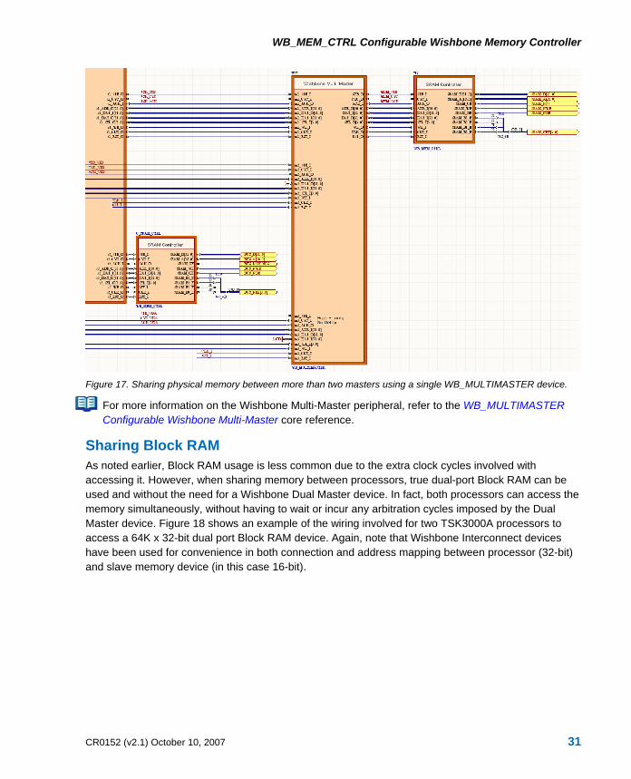
Sharing Block RAM As noted earlier, Block RAM usage is less common due to the extra clock cycles involved with accessing it. However, when sharing memory between processors, true dual-port Block RAM can be used and without the need for a Wishbone Dual Master device. In fact, both processors can access the memory simultaneously, without having to wait or incur any arbitration cycles imposed by the Dual Master device. Figure 18 shows an example of the wiring involved for two TSK3000A processors to access a 64K x 32-bit dual port Block RAM device. Again, note that Wishbone Interconnect devices have been used for convenience in both connection and address mapping between processor (32-bit) and slave memory device (in this case 16-bit).
CR0152 (v2.1) October 10, 2007 31

WB_MEM_CTRL Configurable Wishbone Memory Controller
Figure 18. Sharing true dual-port Block RAM between processors.
32 CR0152 (v2.1) October 10, 2007

WB_MEM_CTRL Configurable Wishbone Memory Controller
Revision History
Date Version No. Revision
14-Dec-2004 1.0 New release
27-May-2005 1.1 Updated for Altium Designer SP4
12-Dec-2005 1.2 Path references updated for Altium Designer 6
13-Oct-2006 2.0 Updated for Altium Designer 6.6 – includes information on device when configured as an SDRAM Controller.
10-Oct-2007 2.1 Updated for Altium Designer 6.8 – includes information on device when configured as a Flash Memory Controller.
Software, hardware, documentation and related materials:
Copyright © 2007 Altium Limited.
All rights reserved. You are permitted to print this document provided that (1) the use of such is for personal use only and will not be copied or posted on any network computer or broadcast in any media, and (2) no modifications of the document is made. Unauthorized duplication, in whole or part, of this document by any means, mechanical or electronic, including translation into another language, except for brief excerpts in published reviews, is prohibited without the express written permission of Altium Limited. Unauthorized duplication of this work may also be prohibited by local statute. Violators may be subject to both criminal and civil penalties, including fines and/or imprisonment. Altium, Altium Designer, Board Insight, Design Explorer, DXP, LiveDesign, NanoBoard, NanoTalk, P-CAD, SimCode, Situs, TASKING, and Topological Autorouting and their respective logos are trademarks or registered trademarks of Altium Limited or its subsidiaries. All other registered or unregistered trademarks referenced herein are the property of their respective owners and no trademark rights to the same are claimed.
CR0152 (v2.1) October 10, 2007 33


![Wishbone Series by Coachingyouthfootball[1]](https://static.fdocuments.in/doc/165x107/5525c56f550346ca3b8b460f/wishbone-series-by-coachingyouthfootball1.jpg)