WAVETEK 2002A SWEEP & SIGNAL GENERATOR - Dudley Lab · serial no. instruction manual model 2002a...
144
Serial No. INSTRUCTION MANUAL MODEL 2002A SWEEP/SIGNAL GENERATOR 0 - 1979 - WAVETEK THIS DOCUMENT CONTAINS INFORMATION PROPRIETARY TO WAVETE K. THE INFORMATION IN THIS DOCUMENT IS NOT TO BE USED OR DUPLICATED IN ANY MANNER WITHOUT THE PRIOR APPROVAL, IN WRITING OF WAVETEK. 66 N. FIRST AVENUE, P.O. BOX 190 BEECH GROVE, INDIANA 46107 31 7-783-3221 Scans by ArtekMedia O 2006
Transcript of WAVETEK 2002A SWEEP & SIGNAL GENERATOR - Dudley Lab · serial no. instruction manual model 2002a...
Serial No.
INSTRUCTION MANUAL
MODEL 2 0 0 2 A SWEEP/SIGNAL GENERATOR
0 - 1979 - WAVETEK
THIS DOCUMENT CONTAINS INFORMATION PROPRIETARY TO WAVETE K. THE INFORMATION I N THIS DOCUMENT IS NOT TO BE USED OR DUPLICATED I N ANY MANNER WITHOUT THE PRIOR APPROVAL, I N WRITING OF WAVETEK.
66 N. FIRST AVENUE, P.O. BOX 190
BEECH GROVE, INDIANA 46107
31 7-783-3221
Scans by ArtekMedia O 2006

ScansBY
Artek MediaArtek Media
1042 Plummer Cir . SWRochester, MN 55902
www.artekmedia .com
"High resolution scans of obsolete technical manuals"
if your looking for a quality scanned technical manual in PDF format please visit
our WEB site at www.artekmedia.com or drop us an email atmanuals @artekmedia.com and we will be happy to email you a current list of themanuals we have available .
If you don't see the manual you need on the list drop us a line anyway we maystill be able to point you to other sources. If you have an existing manual youwould like scanned please write for details, This can often be done veryreasonably in consideration for adding your manual to our library.
Typically the scans in our manuals are done as follows;1) Typed text pages are typically scanned in black and white at 300 dpi .2) Photo pages are typically scanned in gray scale mode at 600 dpi3) Schematic diagram pages are typically scanned in black and white at 600
dpi unless the original manual had colored high lighting (as is the case forsome 70's vintage Tektronix manuals) .
if you purchased this manual from us (typically through our Ebay name ofArtekMedia) thank you very much . If you received this from a well-meaning"friend" for free we would appreciate your treating this much like you would"share ware". By that we mean a donation of at least $5-10 per manual isappreciated in recognition of the time (a manual can take as much as 40 hours toreproduce, book, link etc.), energy and quality of effort that went into preservingthis manual. Donations via PayPal go to : [email protected] or can bemailed to us the address above.
Dave & Lynn HendersonArtek Media

WARRANTY
All Wavetek instruments are warranteed against defects in material and workmanship for a period of one year after date of manufacture. Wavetek agrees to repair or replace any assembly or component (except batteries) found to be defective under normal use during this period. Transfermatic Switch assemblies, manufactured by Wavetek, are unconditionally warranteed for the life of the instrument. Wavetek's obligation under this warranty is limited solely to repairing any such instrument which, in Wavetek's sole opinion, proves to be defective within the scope of the warranty when returned to the factory or to an authorized service center. Transportation to the factory or service center i s to be prepaid by purchaser. Shipment should not be made without prior authorization by Wavetek.
This warranty does not apply to any products repaired or altered by persons not authorized by Wavetek, or not in accordance with instructions furnished by Wavetek. If the instrument i s defective as a result of misuse, improper repair, or abnormal conditions or operations, repairs will be billed at cost.
Wavetek assumes no responsibility for i t s product being used in a hazardous or dangerous manner either alone or in conjunction with other equipment. High voltage used in some instruments may be dangerous if misused. Special disclaimers apply to these instruments. Wavetek assumes no liability for secondary charges or consequential damages and, in any event, Wavetek's liability for breach of warranty under any contract or otherwise shall not exceed the purchase price of the specific instrument shipped and against which a claim is made.
Any recommendations made by Wavetek for use of i t s products are based upon tests believed to be reliable, but Wavetek makes no warranty of the results to be obtained. This warranty i s in lieu of all other warranties, expressed or implied, and no representative or person is authorized to represent or assume for Wavetek any liability in connection with the sale of our products other than set forth herein.
SCOPE OF THIS MANUAL
This manual provides descriptive material and instructions for the installation, operation, main- tenance, and repair of the WAVETEK Model 2002A SweepISignal Generator.
Scans by ArtekMedia O 2006

CONTENTS
SECTION 1 - GENERAL INFORMATION 1.1 IN-TRODUCTION 1.2 SPECIFICATIONS 1.3 OPTlOlVS 1.4 ACCESSORIES
SECTION 2 - OPERATION 2.1 IN-TRODUC-TION 2.2 MECHANICAL INSTALLATION 2.3 ELECTRICAL INSTALLATION 2.4 DESCRIPTION OF FRONT PANEL 2.5 DESCRIPTION OF REAR PANEL 2.6 TYPICAL OPERATING SET-UP 2.7 SPECIAL OPERA-TING NOTES 2.8 PROGRAMMING
SECTION 3 - THEORY OF OPERA'TION 3.1 INTRODUCTION 3.2 BLOCK DIAGRAM 3.3 DPS2A - POWER SUPPLY 3.4 M101B - SWEEP RATE 3.5 M102A - SWEEP DRIVE 3.6 M103A - SWEEP DRIVE 3.7 M104A - LEVELER 3.8 MI05 - MARKER ADDER 3.9 MI09 - SWEEP OSCILLATOR 1 3.10 M l l O - SWEEP OSCILLATORS 2A, 2B, AND 3 3.1 1 MA1 1 1 - OU-TPUT AMPLl F l E R 3.12 MI21 - MODULATOR 3.13 MI31 - BAND SELECT 3.14 MI32 - INTERFACE
SECTION 4 - PERFORMANCE TESTS 4.1 INTRODUCTION 4.2 FREOUENCY RANGE AND ACCURACY -TESTS 4.3 SWEEP WIDTH TEST 4.4 DISPLAY LINEARITY TEST 4.5 SPU RlOUS SIGNAL TEST 4.6 FREOUENCY DRIFT TEST 4.7 BLANKING TEST 4.8 OUTPUT IMPEDANCE AND SWR TEST 4.9 RF OUTPUT MAXIMUM LEVEL TEST 4.10 RF OUTPUT ATTENUATION AND ACCURACY TESTS 4.1 1 R F OUTPUT FLATNESS -TEST 4.12 SWEEP TIME (HORIZONTAL OUTPUT) TEST 4.13 MARKER SYSTEM TESTS 4.14 EXTERNAL PROGRAMMIIVG 4.15 SLOPE TEST 4.16 1 KHz MODULATION TEST 4.1 7 PEN LIFT (OP-TION B4)
Scans by ArtekMedia O 2006

CONTENTS continued
SECTION 5 - MAINTENANCE 5.1 INTRODUCTION 5.2 SERVICE IN FORMATION 5.3 CALIBRATION PROCEDURE 5.4 TROUBLESHOOTING 5.5 FIELD INSTALLATION OF OPTlOlVS
SECTION 6 - REPLACEABLE PARTS 6.1 l IVTRODUCTION 6.2 MANUFACTURERS CODE + + + PARTS LIST
SECTION 7 - SCHEMATICS 7.1 INTRODUCTION 7.2 SCHEMATIC NOTES 7.3 SCHEMATIC INDEX * + + SCHEMATICS
CHANGE INFORMATION, IF ANY, IS LOCATED AT THE REAR OF THIS MANUAL
Scans by ArtekMedia O 2006

SECTION 1 GENERAL INFORMATION
1.1 INTRODUCTION
The Model 2002A covers the 1 to 2500 MHz range in three bands. Band 1 is covered by a 1 to 500 MHz heterodyne sweep oscillator. Band 2 is covered by two fundamental oscillators which sweep from 500 to 1000 NlHz and 1000 to 1500 MHz, respectively. Band 3 i s covered by a single fundamental oscillator sweeping from 1500 to 2500 MHz. Additionally, all four oscillators may be stacked (sequentially swept) to cover the entire 1 to 2500 MHz instrument range (band 4).
Each of the four frequency bands (1 -500 MHz, 500-1 500 MHz, 1500-2500 MHz, and 1-2500 MHz) may be used in three modes of operation: startlstop, Af, or CW. I t can be swept over any portion of a given band, in either direction, a t any rate from 50 sweeps per second to 1 sweep every 100 seconds. Manual, triggered, or recurring sweeps are provided. The sweep frequency, sweep width, and output attenuation may be controlled by external voltages.
Other features of the Model 2002A include a SLOPE control which compensates for frequency dependent varia- tions in the external circuitry, and a 1 kHz square-wave modulator for low-level recovery applications.
This instrument also includes an elaborate frequency marker system. Up to five crystal-controlled birdy marker modules (single frequency or harmonic type) may be plugged into the Model 2002A. Each module has its own front-panel onloff switch. Additionally, a single module producing harmonic markers at 1, 10, 50, and 100 MHz intervals may be installed. Front-panel SIZE and WIDTH controls enable optimum adjustment of the marker display. The marker system features dual-amplitude markers for easy identification. In application, the markers may be tilted up to 90' for easy viewing when displayed with steep transition signals, or they may be rectified by a front-panel switch for X-Y plotter applications.
Other optional features include a rear-panel Auxilliary RF Output and a Pen Lift circuit for use with X-Y plotters.
Most optional features, as well as the functional circuits for the basic sweep generator, have modular plug-in construction. This allows optional features to be factory installed at the time of purchase, or customer installed a t a later date. This concept offers protection against obsolesence, since updated and additional features can be simply and economically added as new test procedures dictate. In addition, maintenance problems can be greatly simplified by stocking several modules instead of hundreds of discrete components.
Scans by ArtekMedia O 2006

1.2 SPECI FICATIONS
1.2.1 FREQLIENCY
RANGE
SWEEP WIDTH
ACCURACY AT 25OC
Band 1 Bands 2,3 Band 4
ACCURACY VS TEMP Bands 1 ,2 Band 3
DISPLAY LINEARITY
BAND SWITCHING
SPURIOUS SIGNALS
HARMOIVICS
NON-HARMONICS
RESIDUAL FM (CW MODE)
DRIFT
BLANKING
1 to 2500 MHz in four bands: 1 -5OOI500-1500/1500-250011-2500
Af - 200 kHz to 500 MHz on all bands
SIS - 200 kHz to 500 MHz on band 1 200 kHz to 1000 MHz on bands 2 , 3 1 MHz to 2500 MHz on band 4
CW ---- Af ----
CENTFREQ SWPWIDTH
15 MHz 30 MHz 50 MHz
500 k HzI0C 1 MHzI0C Frequency scale calibrated in 10 NlHz increments for band 1, 20 MHz increments for bands 2 and 3, and 50 NlHz for band 4. Af sweep width i s calibrated in 10 MHz intervals.
1 % (discounting band switch discontinuities)
Band switching discontinuity points occur at 500, 1000, and 1500 MHz. The discontinuity is -9 + 20 MHz. A band switching blanking output signal (approximately 15 V in magnitude, switchable polarity) occurs at the rear-panel BAND STACKING BLANKING output connector.
SIGNAL FREQUENCY SPURIOUS SIGNAL LEVEL 1 to 10MHz -20 dBc 1 0 to 2500 Nl Hz -30 dBc 1 to 500 MHz -35 dBc (1 to 500 MHz) 1 to 500 MHz -30 dBc (full range) 500 to 2500 MHz non detectable
Bands 1 ,2 Band 3
<10 kHz peak to peak <20 kHz peak to peak
Bands 1, 2 <I00 kHz15 min. <2 MHz18 hr.
Band 3 <200 kHz 15 min. <4 MHz18 hr.
(A t constant temperature after 1 hr. warm-up, and allowing a 5 minute stabilizing period after a frequency change.)
A front-panel switch enables the RF output to be removed during the sweep retrace time to provide a zero volt base line.
Scans by ArtekMedia O 2006

1.2.2 R F OUTPUT
IMPEDANCE
SW R
MAXIMUM LEVEL
ATTENUATION
ACCURACY
FLATNESS A T +13 dBm OUTPUT
SLOPE
OUTPUT COhINECTOR
EXTERNAL LEVELING
1.2.3 SWEEP
OPERATING MODES
SWEEP MODES
SWEEP TIME
SWEEP DWELL
HORIZONTAL OUTPUT
Less than 1.5:1 with insertion loss of 10 dB from STEP ATTENUATOR. Less than 1.3:1 with insertion of 20 dB or more from STEP ATTENUATOR.
Output continuously adjustable from +13 to -77 dBm. 70 dB in 10 dB steps plus a 20 dB vernier.
STEP ATTENUATOR: 3% of attenuation (maximum error at 70 dB = k2.1 dB). VERNIER ATTENUATOR: k . 5 dB over top 13 dB of range, lower 7 dB i s unspecified.
Up to 21 dB/GHz of slope may be imposed on the RF output via the front-panel SLOPE control. The reference (pivot point) of this slope i s 1 MHz. The output METER will indicate the change in output level at slow sweep rates. IVOTE: The OUTPUT VERNIER must be set so that the added slope will not produce an R F output level greater than the highest possible OUTPUT VERN l ER setting.
An external negative monitor signal, between .2 and 2 volts, may be used to level the RF output.
Repetitive sweep Single sweep Externally triggered sweep Manual sweep Line-locked sweep
Continuously variable from less than .O1 to more than 100 seconds per sweep in four decade ranges with vernier (add 1 msec for every band switch point crossed). Manual and line-locked sweep are also provided. NOTE: In l ine-locked sweep, the sweep time for band 4 i s double that for bands 1, 2, and 3.
Approximately 4 msec delay at start of sweep controlled by rear-panel switch.
Zero to +10 volts. Impedance 10 k n .
Scans by ArtekMedia O 2006

1.2.5 MARKER SPECIFICATIONS
TYPE
EXTERNAL
INTERNAL
Single Frequency
Harmonic (comb)
ACCURACY
WIDTH
SIZE
DUAL AMPLITUDE FEATURE
Square-wave modulation produces blanking of RF output a t a 1 kHz rate for low-level recovery operations. Onloff control is provided on the front panel.
For external AM and FM, refer to Section 1.2.6, Remote Programming.
Birdy by-pass
Front-panel BNC connector accepts external CW signal for conversion to a birdy marker. Input level: 100 mV into 50 ohms. Front-panel onloff control is provided.
The instrument has provisions for either single frequency or .harmonic type plug-in birdy marker modules. Maximum of five A1 or A2 options and one A3 option.
A1 options are individually controlled by front-panel push buttons.
A2 or A3 options provide markers at multiples of the speci- fied fundamental frequency.
A2 options produce harmonics of one crystal frequency and are individually controlled by front-panel push buttons.
A3 option is a combination 1, 10, 50, and 100 MHz harmonic marker controlled by a front-panel rotary switch.
Option A1 or A2 .005% at 25OC .007%, O0 to 50°C
Option A3 .005%, O0 to 50°C
Adjustable in four steps from approximately 15 to 400 k H z.
The instrument i s capable of providing markers a t two distinct amplitudes to facilitate marker identification. An internal adjustment controls the ratio of the two sizes.
Markers controlled by front-panel buttons a, b, c, and EXT (first, second, third, and sixth from left) are full-size, whereas markers controlled by buttons d and e can be set for some fraction of this size.
This feature pertains to the Deluxe Harmonic Marker (Option A3) in the following manner.
Setting Reducible Full size
1 MHz 10 MHz 50 MHz
10 MHz 100 MHz 100 MHz 100 MHz
Scans by ArtekMedia O 2006

AMPLITUDE CONTROL
R EC-TI FICATION
1.2.6 REMOTE PROGRAMMING
BAND SELEC-TION
FREQUENCY
SWEEP WIDTH
VERNIER, 0-20 dB OUTPUT
EXTERNAL AM
All markers are continuously adjustable with front-panel controls over two ranges. he ranges for full-:ize markers are: 4 Vpp to 10 mVpp and 25 mVpp to 50 pVpp. (Voltages are approximate.)
Birdy markers can be rectified (positive) for use with X-Y plotters. Size varies with detector's impedance. Adjustable from approximately 2 V to 1 mV with detector impedance of 1 Megohm, or from 0.2 V to 1 mV with detector impedance of 0 ohms.
This feature adds to the normally vertical marker a hori- zontal component with an amplitude of about 10% of horizontal scope display. The marker amplitude control affects only the vertical component; therefore, the marker is adjustable from a horizontal position to an angle approaching vertical as the MARKER SIZE control setting i s increased.
A rear-panel PROGRAMM l NG jack provides necessary connections for remote control of frequency, sweep width band selection, and the 0 to 20 dB vernier output level. This jack also provides connections for external amplitude and frequency modulation and external triggering of the sweep rate generator, as well as cor~nections to internal DC voltages, and sweep and blanking signals.
Selection i s accomplished via TTL signals or contact closure.
May be remotely programmed within the selected band by applying a voltage between + I0 V and -10 V (-10 V programs the low frequency end of band).
Tuning sensitivities are:
band 1 35.7 mV/MHz band 2,3 17.8 mV/MHz band 4 7.1 mV/MHz
May be controlled with a remote potentiometer.
May be controlled by setting the front-panel OUTPUT VERNl ER for maximum output and applying a DC voltage between 0 and -4.5 V (-4.5 V programs 20 dB reduction in power). Front-panel METER will indicate the RF output level. Simultaneous AM and level control can be achieved by adding the appropriate DC offset to the modulating signal. See "External AM".
Amplitude modulation can be accomplished according to the specifications below. Simultaneous AM and level control can be achieved by adding the appropriate DC offset to the modulating signal. See "Vernier 0-20 dB Output".
Scans by ArtekMedia O 2006
FREQUENCY RANGE
SENSITIVITY
MAXIMUM MODULATION %
EXTERNAL FM
1.2.7 GENERAL
OPERATING TEMPERATURE
POWER REQUIREMENTS
DIMENSIONS
WEIGHT
1.3 OPTIONS
DC to 10 kHz (3 dB bandwidth)
1 Vpp per 10% AM
Varies from 10% to 90% depending upon the setting of the OUTPUT VERNIER control as shown in Figure 2-16. Overmodulation will cause the front-panel LINLEVELED light to turn on; however, since the unleveled condition would exist only a t the peak or trough of modulation, the light will be less than full intensity.
Any portion of any band not containing a band switching discontinuity point can be swept a t any rate up to 10 kHz. +50 MHz deviation can be obtained a t rates up to 50 kHz. Modulation rates up to 200 kHz are possible with reduced deviation and unspecified linearity. Tuning sensitivity is the same as that for remote frequency control.
115 or 230 VAC +lo%, 50 to 400 Hz, approximately 25 VA.
30.3 cm wide x 13.4 cm high x 34.9 cm long (12" x 5%" x 13 %")
10.5 kg (23 Ibs.) net 12.7 kg (28 Ibs.) shipping
All options are factory or field installable. A maximum of 5 A1 or A2 options can be installed in the instrument in addition to 1 each of Options A3, B4, and B5.
Single Frequency Marker a t any frequency within the instrument range.
Harmonic (comb) Marker a t 1, 5, 10, 50, or 100 MHz intervals (other intervals available on special order). Also available is a Dual Harmonic Marker a t 0.111 NlHz intervals (occupies two marker sockets).
NOTE: Operating range of A2 options is 1 to 1500 MHz.
Deluxe Harmonic Marker a t 1, 10, 50, and 100 MHz intervals over entire instrument range.
Pen Lift provides contact closure during forward sweep trace. Binding post terminals are provided on rear panel.
Auxilliary R F Output provides rear-panel R F output signal (approximately -10 dBm, depending on marker options installed) for driving a frequency counter or other similar purpose.
Scans by ArtekMedia O 2006

1.4 ACCESSOR l ES
1.4.1 FURNISHED WITH INSTRUMENT
INS-TRUCTIOIV MANUAL
PROGRAMNIING PLUG
1.4.2 AVAl LABLE AT EXTRA COST
WIDE BAND RF DETECTORS
RACK MOUNT KIT
SERVICE KIT
Connector and pins provided to mate with jack on instru- ment rear panel.
Model D l 53. Frequency range: 1 MHz to 12.4 GHz.
K108 enables instrument to be mounted in a standard 19" wide instrument rack.
KO05 provides a module extender, extension cables and adaptor.
Scans by ArtekMedia O 2006

SECTION 2 OPERATION
2.1 INTRODUCTION PROCEDURE
This section provides complete installation and operating instructions for the Wavetek Model 2002A. The instructions include information on mechanical installation, electrical installation, front-and-rear-panel features, oper- ating procedures, and programming instructions.
Remove screws from one side panel. Mount items A and B against side panel of the instrument and secure with screws provided. Repeat for other side of unit. If rack mount ki t is removed from unit, use screws originally in side panels to avoid possible internal damage.
2.2 MECHANICAL INSTALLA'TION 2.3 ELECTRICAL INSTALLATION
2.2.1 INITIAL IIVSPECTION 2.3.1 POWER REQUIREMENTS
After unpacking the instrument, visually inspect external parts for damage to knobs, connectors, surface areas, etc. The shipping container and packing material should be saved in case it i s necessary to reship the unit.
This instrument operates from either 11 5 VAC or 230 VAC supply mains, as selected by the rear-panel AC LlNE switch. Before operating this instrument, be sure that the AC LlNE FUSE is the correct value for the selected voltage (see Section 2.5).
2.2.2 DAMAGE CLAIMS The Power Supply has been designed to operate over a 50 to 400 Hz line frequency; however, the line operated sweep rate function must be adjusted to the line frequency.
I f the instrument received has been damaged in transit, notify the carrier and either the nearest Wavetek area representative or the factory in Indiana. Retain the shipping carton and packing material for the carrier's inspection. Instruments are shipped from the factory set up to operate
at 115 VAC, 60 Hz unless otherwise specified. The local representative or the factory will immediately arrange for either replacement or repair of your instrument without waiting for damqge claim settlements.
2.3.2 PERFORMANCE CHECKS
The electrical performance of this instrument should be verified prior to actual use. Performance checks for incoming inspection are given in Section 4 of this manual.
2.2.3 RACK MOUNTING (K108)
CONTENTS (See Figure 2-1).
PART NO. ITEM QTY
A (Insert) B (Side) C (Screw) D (Screw)
Scans by ArtekMedia O 2006

Figure 2-1. K108 Rack Mount
F igure 2-2. Front Panel
Scans by ArtekMedia O 2006

2.4 DESCRIPTION O F FRONT PANEL
Refer to Figure 2-2.
(1 ) BAND switch selects desired frequency band.
(2) CENTER FREQISTART thumbwheel controls center frequency when MODE switch is set to Af or CW, and start frequency when MODE switch is set to S/S.
(3) MARKER WIDTH, SlZE controls; outer ring selects marker width (4 positions); inner knob varies marker amplitude.
(4) FREQUENCY SCALE shows center frequency and sweep width, or startlstop frequencies (depending on posi- tion of MODE switch). Graduated for all 4 bands.
(5) HARMON lC MARKER switch selects markers generated by the Deluxe Harmonic Marker (Option A3). If this option i s not installed, this knob has no function.
(6) SWEEP TIME, VARIMANUAL controls; outer ring selects sweep time range (4 ranges); line rate, or manual control; inner knob provides manual frequency sweeping with the outer ring set to MANUAL, and vernier control of the sweep time with the outer ring set to any of the 4 sweep time ranges.
(7) SWEEP WIDTHISTOP thumbwheel controls sweep width when MODE switch is set to Af, and stop frequency when MODE switch is set to SIS. When the MODE switch is set to CW, this control has no function.
(8) MODE switch selects SIS (StartIStop), Af, or CW mode.
(9) OUTPUT VERNIER, STEP ATTENUATOR; outer ring controls RF output over a 70 dB range (+I0 to -60 dBm) in 10 dB steps; inner knob provides vernier control (+3 to -17 dB) of RF output.
(10) METER indicates RF output over a 20 dB range (calibrated from +3 to -1 0 dB). The METER reading added algebraically to the STEP ATTENUATOR indication is the RF output of the instrument.
(1 1) UIVLEVELED lamp signals when the METER reading is not valid.
(1 2) R F OUT connector (type N) provides connection for RF output signal.
(1 3) SLOPE control provides compensation for frequency dependant level variations external to the instrument.
(14) ALC switch closes the internal leveling loop when in the INT position. In the EXT position, an external monitor may be used to control the instrument's RF output (through the ALC IN connector). If the switch is in EXT, and no external monitor i s used, the RF output i s unleveled and the OUTPUT VERNIER has no effect.
(15) ALC IN connector (type BNC) accepts an external leveling control signal from a remote monitor when the ALC switch i s in the EXT position.
(16) BLANKING switch allows the RF output to be blanked during sweep retrace when the switch is in the ON position. When the switch i s not on, the RF output i s
displayed during retrace.
(1 7) TRIGIRECUR switch selects either recurring sweep of the time selected by the SWEEP TIME control (with MODE switch in Af or SIS), or triggered sweep, either manually or with an external source (the external trigger input i s pin 7 of the rear-panel PROGRAMMING jack). Manual triggering i s accomplished by pushing the TRIGIRECUR switch to i t s full up (momentary) position.
(18) MARKER IN connector (type BNC) accepts an external CW signal to produce a marker a t the external frequency on the display.
(19) MARKER switches select which internal markers are active (marker -Frequency is engraved on pushbutton). The furthest right switch selects internal square wave modulation.
(20) DEMOD IN connector (type BNC) accepts demodulated swept signal from device under test so that markers can be added (the combined signal is available a t the VE RT OUT connector).
(21) VERT OUT connector (type BNC) provides vertical display signal (demodulated signal plus markers i f DEMOD IN is used) for display oscilloscope.
(22) HORlZ OUT connector (type BNC) provides a 0-10 V Triangle wave for driving the display oscilloscope horizontal channel.
(23) MARKER SlZE switch selects large (-7 mVpp to 3.5 Vpp) markers, small (-0.2 mVpp to -20 mVpp) markers, or rectified (-0.2 mV to 1.25 V) markers (the marker ampliude i s varied by means of the MARKER SlZE control). The rectified markers are designed for use with X-Y recorders.
(24) POWER switch applies AC power to the Power Supply. Pilot light indicates operation.
Scans by ArtekMedia O 2006

(25) TILTINORM switch provides vertical markers in the NORM position, and horizontal markers of fixed amplitude (10% of horizontal display) in the TILT position when the MARKER SlZE control is set to minimum. Increasing the setting of the MARKER SlZE control will cause the horizontal markers to t i l t toward a vertical position. This feature i s helpful in identifying frequencies on steep response curves.
2.5 DESCRIPTION OF REAR PANEL
Refer to Figure 2-3.
(1) AUX RF OUT connector (type BNC, Option B5) provides approximately -10 dBm R F output.
(2) B LAN K l NG output connector (type BNC) provides pulse for oscilloscope intensity input to remove band stacking transition points from scope display. Switch selects pulse polarity.
(3) SWEEP DWELL switch selects normal or delayed (approximately 4 msec) sweep.
(4) AC LlNE cord provides connection to AC mains via 3 prong plug.
(5) AC LlNE switch enables unit to operate from either 115 VAC or 230 VAC supply mains.
( 6 ) AC LlNE FUSE is time delay; 1.0 amp for 115 VAC operation, 0.5 amp for 230 VAC operation.
(7) PEN LIFT (Option B4) binding posts provide contact closure during forward sweep when the front- panel SWEEP TIME control i s in the 1-10 sec, 10-100 sec, or MANUAL range. In all other ranges, and during retrace, the contacts are open. NOTE: In MANUAL sweep, there i s no retrace signal, so the contacts are continually closed.
(8) PROGRAMMING PLUG provides input connections for external trigger, sweep delay, external AMIFM, and remote control of center frequency, sweep width, band selection and R F output. Output connections are provided for sweep ramp, retrace blanking, and Power Supply voltages.
NOTE
If Options B4, B5 are not installed, blank plug buttons will be installed in the rear panel instead of the indicated connectors.
F i g u r e 2-3. Rear Panel
Scans by ArtekMedia O 2006
2.6 TYPICAL OPERATING SET-UP
When initally setting up the instrument, first check the rear-panel AC LlNE FUSE and switch to be sure the instrument i s set for operation with the available AC mains.
Make connections between the instrument, the device under test, and the oscilloscope as shown in Figure 2-4. Since hum, RF leakage, and spurious signal pick-up must be kept to a minimum, it is essential that good connections and grounds be maintained throughout the entire set-up. Use coaxial cables with BNC connectors wherever possible. The RF output cable i s especially critical. It should have a characteristic impedance of 50 ohms, and should be kept as short as practical (under 3 feet). If the input impedance of the device under test is not 50 ohms, a matching network, as shown in Figure 2-4, should be used to ensure a constant amplitude input signal to the device under test.
After the RF signal passes through the RF circuit of the device under test, it must be demodulated before being connected to the DEMOD IN of the instrument. I f a demodulator is not a part of the device under test, one must be added externally (see Figure 2-4). The input impedance of the demodulator must present the proper load to the RF circuit beirlg tested. The Wavetek Model Dl53 RF Detector i s recommended for 50 ohm applications.
Turn the front-panel POWER switch on. The pilot light should indicate an operating condition.
NOTE
This instrument does not require a warmup period unless it is to be used at the extreme limits of its specifications.
After completing the set-up, adjust the instrument front- panel controls for the required center frequency, sweep width, output amplitude, and sweep rate. Turn the desired markers on and adjust their size and width.
2.7 SPECIAL OPERATING NOTES
does not change the response, a true response has been obtained.
2.7.2 EFFECTS FROM OVERLOADING
The use of excessive signal from the instrument can overload the receiver circuits. To assure that this condition i s not present, and that the response is a true representation of the device under test, turn the OUTPUT STEP and VERNIER controls to minimum output amplitude. Gradual1 y increase the output amplitude until a response i s obtained. Further increasing the output amplitude should not change the configuration of the response envelope does change, such as flattening a t the top, decrease the output just far enough to restore the proper configuration.
2.7.3 MAKING MEASUREMENTS AT LOW LEVEL
When making measurements a t low levels, radiation and ground loops become problems. Using double shielded cables for cables carrying RF signals helps minimize the radiation problem. Ground loops causing hum pick-up can sometimes be eliminated by completing only one ground connection between each instrument. This applies particularly to the scope horizontal input. I f the ground connection is made at the vertical input terminial, an addi- tional ground a t the horizontal input terminal will often result in hum pick-up.
2.7.4 SWEEP DWELL
In order to stabilize external circuits (such as when using a network analyzer), it is sometimes desirable to turn the RF signal on prior to the start of the sweep. This can be accomplished using the rear-panel SWEEP DWE LL switch. When the switch is turned on, the RF output i s tuned on approximately 4 msec before the sweep begins.
This applies only to the four variable time positions of the SWEEP TIME control, and does not apply to either the LlNE or MANUAL position.
2.7.1 ERRORS FROM SWEEP RATE EFFECTS
2.7.5 OPERATlOlV WITH X-Y PLOTTERS When sweeping R F circuits having rapid amplitude changes, errors may occur, due mainly to detector delays. Decreasing the detector output time constant will minimize this effect. Figure 2-5 illustrates sweep rate effect.
To check for sweep rate effect, first set the sweep width to i t s lowest practical setting, then reduce sweep time while closely observing the swept output response. Any change in the response indicates the sweep rate is too fast for a true response. When a further reduction of sweep time
Two features are incorporated into the instrument to facilitate operation with X-Y plotters.
First, a marker clamp switch (part of the front-panel MARKER SIZE switch) which converts the high frequency marker signals to lower frequencies, compatible with the operating speed of the marker pen.
The second feature (Pen Lift) i s available as Option B4, and is described in Section 2.8.4.
Scans by ArtekMedia O 2006

MODEL 2 0 0 2 A
F i g u r e 2-4. T y p i c a l T e s t Set-up
SCOPE
n OV H .
RESPONSE
RESPONSE WITH SLIGHT ERROR DUE T O SWEEP RATE BEING
LARGE ERROR DUE TO SWEEP RATE BEING FAR TOO FAST
F i g u r e 2-5. Sweep Rate Effects
I 1
0 I 0
l o o o l 0 0 0 ~ 0 0
H O R l Z V E R T D R F OUT
0 0 0 Q 0 O o O O
;' Partially #eveled
.)
I
F i gure 2-6. E x t e r n a l Moni t o r Output S ignal
b 6
Scans by ArtekMedia O 2006
- RF DET
h
MATCH NTWK
-UNDER
h
DEVICE
T E S T

2.7.6 OPERATION WITH EXTERNAL MONITOR
Operation with an external monitor can produce a flatter (less amplitude variation) input signal to the device under test than i s obtainable with the internal monitor, since the monitor point i s located a t the point where greatest flatness i s desired and i s not affected by cable VSWR or input impedance of the device under test. Another application i s
to level a t the output point of a wide band power amplifier in. order to increase the output power capability of the sweep generator.
To operate with an external monitor, first set the OUTPUT STEP and VERNIER controls for maximum (+I3 dBm). Next, connect the output from the external monitor to the front-panel ALC IIV connector and set the ALC switch to the EXT poisition. The signal from the external monitor must be of negative polarity between 0.2 and 2 volts. I f the signal i s larger than 2 volts, use a resitive divider to obtain the less-than-2 volts signal. While observing the output from the monitor on an oscilloscope, adjust the OUTPUT VERNIER until the monitor signal becomes leveled (refe? to Figure 2-6).
2.7.9 PEN LIFT (OPTION 64)
This option provides a contact closure during forward sweep time. During retrace, the contacts are open. This option can be used to operate the pen l i f t of an X-Y plotter. It is active only during the two slowest settings of the SWEEP TIME switch (1 to 10 seconds and 10 to 100 seconds) and during manual sweep. (During manual sweep the contacts are always closed.) The connections for Option 64 are two binding posts on the instrument rear panel.
2.7.10 AUX RF OUT (OPTION 65)
This option provides an RF signal a t approximately -10 dBm through a rear-panel connector. This signal is identical in frequency and sweep characteristics to the signal from the front-panel RF OUT connector; however, there is no provision for controlling the level of the auxilliary signal. (The actual output level of the auxilliary signal i s depen- dent on the number of marker options (A l , A2, A3) installed in the instrument. The more marker options, the lower the output level.) Likewise, the auxilliary signal will show FM, but will not show AM.
NOTE NOTE
If the requirement of a 0.2 to 2 V monitor signal results in overloading of the device under test, insert an external attenuator pad between the monitor and the device under test.
2.7.7 SLOPE
Up to 41 dB/GHz amplitude slope may be introduced to compensate for frequency-dependant variables in the test system external to the instrument. The pivot point for the slope is 1 MHz, with the maximum amplitude change due to slope introduction being 42.5 dB a t 2500 MHz (refer to Figure 2-7).
When the front-panel SLOPE control i s set to i t s
mid-position adjustment (0 slope), an uncorrected signal will be displayed.
2.7.8 1 KHz MODULATION
This feature provides 1 kHz square wave modulation of the RF output signal. On/off control is provided by a push button switch on the instrument's front panel. The 1 kHz modulating frequency may be adjusted using the control located on top of module M I 21 (see Figure 5-22).
For proper marker operation, the AUX R F OUT connector must be either connected to a 50 ohm device, or terminated in 50 ohms (terminator provided).
2.8 PROGRAMMING
Connections for remote control of output level, center frequency, sweep width, band selection, and sweep triggering, and also external AM and FM are provided in the rear-panel PROGRAMMING jack. The jack and i t s pin functions are detailed below (refer to Figure 2-8).
2.8.2 OUTPUT PINS
The first group of pins are voltage and signal outputs. Pin 1 is a common ground. Pins 2 and 3 provide + I0 V, used for remote frequency tuning. Pins 4 and 5 are the 418 V main regulated supplies, and can be used in external applications which draw less than 50 mA each.
Pin 8 is the sweep ramp with varies over a 410 V range. This signal is similar to the signal from the front-panel HORlZ OUT connector, except that the latter ranges from 0 V to +10 V. These ramps are independent of frequency and sweep width.
Scans by ArtekMedia O 2006

0 0 0 0
a 0 0 a m m a 0 a . a 0 a . a a m . m e * . a * .
F i g u r e 2-8.
FNEQ ( P D I Z )
F i g u r e 2-7. S lope
PIN FLINCTION 1 Outputs
1 Ground 2 +10 v 3 -10 v 4 -18 V 5 +18 V 8 Sweep Ramp 14 R e t Blanking 25 Sync 26 1 v/GHz Ref
I1 Normal 9 n 10 Cent Freq
11 n 1 2 Sweep Vid th 15 n 1 6 ~ t a r t / ~ t o p 18 n 19 Band S e l e c t
PIN FUNCTION 111 1Jnused
13,17,27-36 Unused I V I n p u t s
6 Output ~ e v e l / A M 7 Ext T r i g g e r 10 Cent Freq 12 SW/FM/$ L O C ~
21 Band 2B 22 Band2A 23 Band 3 24 Band 4
P i n 20 i s i n t e r n a l t i e p o i n t . Do n o t u s e e x t e r n a l l y .
PROGRAMMING P l u g P i n C o n f i g u r a t i o n
Scans by ArtekMedia O 2006

EXTERNAL FM (PIN 12) Pin 14 provides a retrace blanking signal for a display oscilloscope. The levels at this connector are +16 V (RF off) and -16 V (RF on).
Pin 25 provides a TTL "high" signal whenever the RF output frequency crosses a band switching discontinuity point (500, 1000, 1500 MHz). A t all other times, the output i s TTL "low". This signal finds use in working with network analyzers.
Pin 26 i s a 1 VIGHz reference which provides an indication of the instantaneous RF output frequency. I f the RF output frequency i s 1200 MHz, pin 26 will be +1.2 V. I f the RF output i s swept from 1600 to 2400 MHz, the voltage at pin 26 will follow the frequency, producing a +1.6 V to +2.4 V ramp.
For FM, remove the pin 11 to 12 jumper and connect the modulating source as shown in Figure 2-1 1.
The FM signal should have an average potential of 0 V. Frequency sensitivity i s 35.7 mV1MHz for band 1, 17.8 mV1MHz for bands 2 and 3, and 7.1 mV1MHz for band 4. Maximum frequency deviation as a function of modulating frequency i s shown in Figure 2-12.
The peak amplitude of the modulating signal plus the DC voltage applied to pin 10 of the PROGRAMMING jack should not exceed + I 0 V, since a greater voltage would cause the instrument to sweep beyond i t s band limits.
PHASE LOCK (PIN 12) 2.8.3 NORMAL OPERATION PlNS
The second group of pins is used to provide normal front- panel operation of the instrument. Pin 9 i s jumpered to pin 10, pin 11 i s jumpered to pin 12, pin 15 is jumpered to pin 16, and pin 18 is jumpered to pin 19. A plug containing these jumpers must be installed on the rear-panel PROGRAMMIIVG jack in order to accomplish normal operation.
2.8.4 UNUSED PlNS
The third group of pins i s unused.
2.8.5 INPUT PINS
The functions of the last group of pins are as follows:
REMOTE FREQUENCY CONTROL (PIN 10)
Normal front-panel control of center frequency is provided by a jumper wire between pins 9 and 10 of the rear-panel PROGRANIMIIVG plug. To remotely control the center frequency, remove the jumper and connect pin 10 to the external control, as shown in Figure 2-9.
When the instrument i s operated in a closed-loop synchro- nizing system, the correction voltage i s applied to pin 12 of the PROGRAMMING jack. Again, the MODE switch must be set to Af and the pin 11 to 12 jumper must be removed (refer to Figure 2-1 3).
REMOTE OUTPUT LEVEL (PIIV 6 )
For remote control of the 0 to 20 dB OUTPUT VERNIER control range, first adjust the front-panel OUTPUT VERNIER control fully clockwise. This will produce a METER reading of 3. Connect the external level control .as shown in Figure 2-14. The program level will be indicated on the front-panel METER.
EXTERNAL AM (PIN 6 )
To produce AM, connect the modulating source to pin 6, as shown in Figure 2-1 5.
The modulating frequency may vary over a 0 to 10 kHz (at 3 dB point) range. The modulation sensitivity is 1 Vppl 10% modulation. The maximum % AM is dependent upon the front-panel OUTPUT VERhll ER setting, as shown in Figure 2-16.
REMOTE SWEEP WIDTH CONTROL (PIN 12) EXTERNAL TRIGGER (PIN 7)
Normal control of sweep width i s provided by a jumper between pins 1 1 and 12 of the rear-panel PROGRAMNIING plug. To remotely control the sweep width, remove the jumper and connect pin 12 to the external control, as shown in Figure 2-10.
NOTE
When using the instrument with remote control of sweep width, external FM, or in phase lock operation, the front- panel MODE switch must be set to Af.
The Sweep Time circuit may be remotely triggered by applying a +10 V pulse to pin 7 of the rear-panel PROGRAMMING plug. For proper operation, the front- panel SWEEP TIME control must be set to one of the four variable time positions, and not to MANUAL or LINE. The TRIGIRECUR switch must be set to TRIG. The repe- tition rate of the external tirgger should be slower than the frequency repetition rate set by the front-panel SWEEP TIME and VARIMANUAL controls.
Scans by ArtekMedia O 2006

- HIGH
+ l o - 1 0 CTL CKT
F i g u r e 2-9. Remote Cen te r Frequency C o n t r o l
MODULATI SOURCE
EXTERNAL SWEEP W I DTlI
T O SWEEP WIDTH CTL CKT
F i g u r e 2-10. Remote Sweep Wid th C o n t r o l
EXTERNAL
NG D E V I A T I O N CONTROL
- -
1 - \L TO SWEEP - WIDTH -
CTL CKT
F i g u r e 2-11. E x t e r n a l FM
1 0 0 1 5 0
MODULATION FREQ ( MHz)
F i g u r e 2-12. Maximum FM D e v i a t i o n
Scans by ArtekMedia O 2006

REMOTE BAND SELECTION (PINS 21-24)
For remote control of band selection, remove the jumper between pins 18 and 19 on the PROGRAMiVllNG plug. Any frequency band may now be selected by applying a ground (contact closure or TTL) signal to pin 21,23, or 24 on the PROGRAMMIIVG plug. Applying a ground signal t o pins 21 and 22 simultaneously will select the second half of band 2 (1000-1 500 MHz) (see Section 3.13). If no ground signal i s applied, band 1 will be selected.
CORRECTION VOLTAGE
O P T 1 ONAL S E N S I T I V I T Y
T O SWEEP
- - WIDTH C T L CKT
EXTERNAL L E V E L
1 0 K CONTROL
- - - 1 0 C T L CKT
F i g u r e 2-14. Remote Leve l C o n t r o l
F i g u r e 2-13. Phase Lock
MODULATING
F i g u r e 2-15. E x t e r n a l AM
5 MODULATION CONTROL
S O U R C E
E.laximum . . . . . . Modulation % 50 70 80 90 70 50 10
Output Meter -15-10 -5 0
F i g u r e 2-16. Maxirnuni % AM
Scans by ArtekMedia O 2006
I f 1 I I I S c a l e 1 1 ' 1 1

SECTION 3
3.1 INTRODUCTION
This section first presents an overall block diagram view of the Model 2002A, followed by a more detailed description of each module and assembly.
Before beginning the actual circuit descriptions, it would be well to become familiar with the mechanical arrangement of the instrument. This will enable the block diagram and circuit descriptions to be associated with the physical locations in the instrument, providing a better overall understanding of the instrument (refer to Figure 5-22).
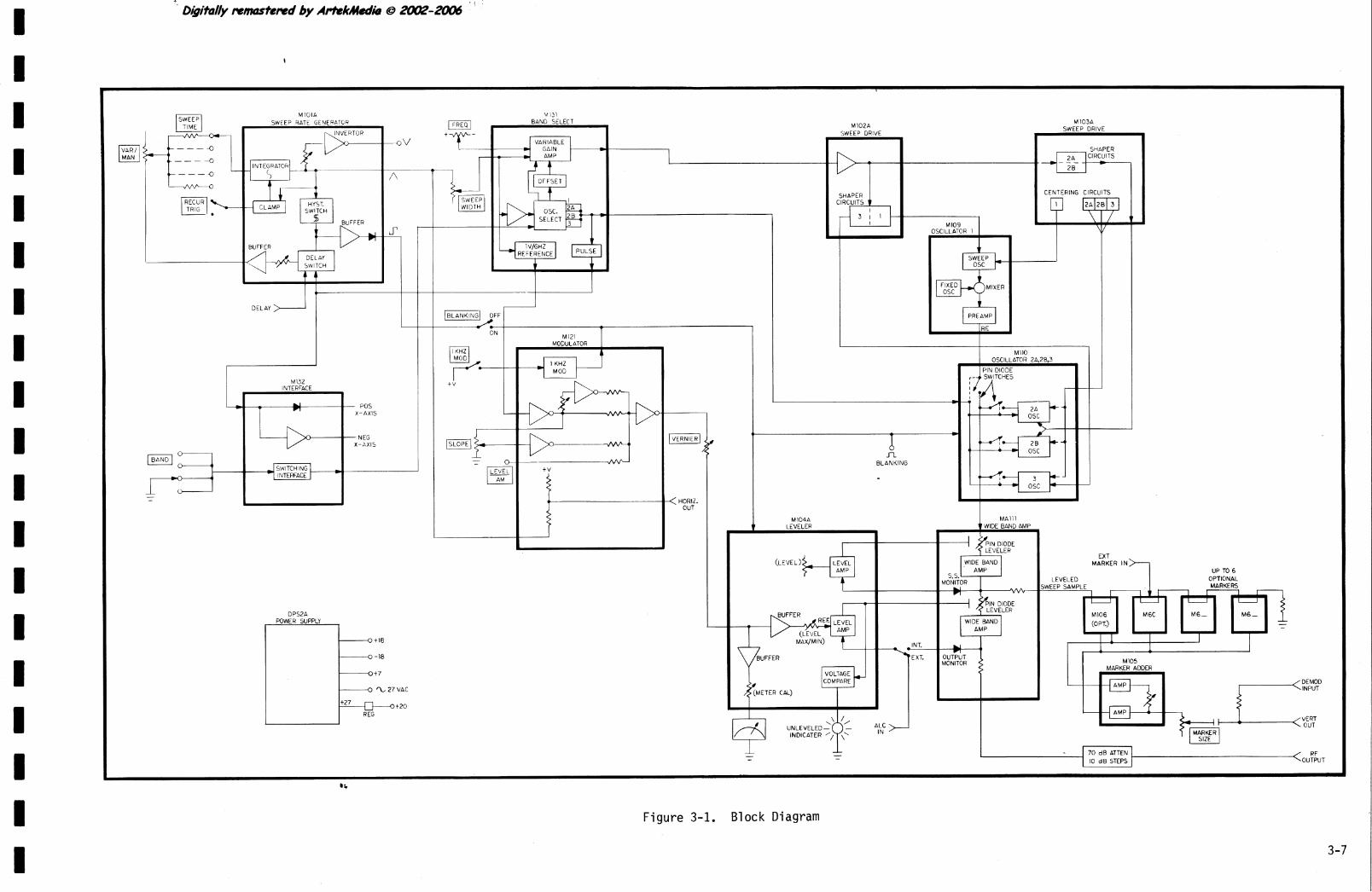
3.2 BLOCK DIAGRAM
The block diagram in Figure 3-1 contains both block and module information. The blocks contained within each module are indicated by the module outline.
The general operation of the Model 2002A is as follows:
The front-panel CENT FREQ and SWEEP WIDTH control settings are fed into the M102A and M103A Sweep Drive modules, where they are combined into a single signal. This signal (sweep drive) i s used to drive the varactor diodes in the appropriate Sweep Oscillator (M 109 or M 1 10). Necessary level shifting, shaping, and amplitude control are accomplished in the Sweep Drive modules.
The Sweep Oscillator output i s fed into the MA1 11 Wide Band Amplifier, and then through the Step Attenuator to the RF output. Leveling i s accomplished by a monitor diode in the MA1 11 which compares the output level to a reference voltage supplied by the OUTPUT VERNIER. Any error i s amplified in the M104A Leveler module, and correction is made at the PIN diode leveler in the MA1 11.
The marker circuit i s composed of the MI05 Marker Adder module, the M6C External Marker module, and the various marker options selected by the customer. The marker circuit uses a sample of the R F signal (sweep sample) which is also leveled in the M104A Leveler. This leveling not only provides a constant-amplitude sweep sample signal to the marker circuit, but also standardizes the sweep sample signals in all instruments, assuring proper operation of field installed marker options.
THEORY OF OPERATION
More detailed descriptions of the individual modules and assemblies are provided below. Schematics are in Section 7.
3.3 DPS2A - POWER SLIPPLY
The Power Supply provides DC power for the rest of the instrument, and a 27 VAC signal to the M1O'IB Sweep Rate Generator module.
The transformer steps the line voltage down to 27 VAC, a level which can be used by the DC-producing circuits. (A portion of this 27 VAC signal i s sent to the MlOlB for use in the line rate sweep function of the instrument.) Fullwave rectifiers and filter capacitors convert the AC signal to DC.
A portion of this 27 VDC signal i s sent to the +20 V regulator mounted on the instrument chassis, the rest is sent to the +I 8 V and +7 V supply circuits.
The +18 V circuit has a temperature-compensated pre- cision voltage reference. This reference is compared to the output voltage by an error amplifier which corrects any error in the output voltage.
The -1 8 V circuit compares the +18 V and -1 8 V outputs and holds the difference in their magnitudes to zero.
The +7.3 V circuit uses a three-terminal adjustable voltage regulator IC to provide a pre-regulated +7.3 V output. This voltage supplies other voltage regulators throughout the instrument.
3.4 MlOlB - SWEEP RATE
IIVTRODUCTION
This module generates the basic sweep ramp for the instru- ment, an inverted ramp used in S/S mode, and a synchro- nous square wave used for blanking.
The M l 01 B is basically a hysteresis oscillator, consisting of a hysteresis switch (IC5A) and an inverting integrator (IC1 with C9). The sweep ramp is the integrator output, while the inverted ramp (derived from the sweep ramp) is the output of an inverting buffer (IC2).
Scans by AHekMedia O 2006

SWEEP RAMP SWEEP DWELL
Diodes CR17 and CR18 clip the hysteresis switch output to produce a "10.6 V square wave. CR13 and CR14 reduce the level to 4 1 0 V, and also provide temperature compensation. -The + I 0 V square wave is positively fed back to the non-inverting input of the hysteresis switch along with delayed negative feedback from the integrator.
When the negative feedback outweighs the positive feed- back, the non-inverting input crosses the ground reference on the inverting input and the switch changes state. This occurs when the hysteresis switch output and the sweep ramp are equal in magnitude but opposite in polarity. The switch output is buffered by IC6B and sent through the sweep time resistor network to pin 10 of the module, the inverting integrator input.
SWEEP TIME
Sweep time i s the time required for the sweep ramp to rise from -10 V to +10 V, and i s determined by the current fed into the inverting integrator input. Sweep time is selected by the front-panel SWEEP TIME control, and i s calibrated by the Freq. Adj. control (R60).
TRIGGERED SWEEP
For operation in recurring sweep mode, +18 V i s applied
to pin 2 of the module. For triggered sweep mode, this voltage i s removed, shutting off Q2 and removing the reverse bias on CR12. This lowers the hysteresis switch trip point to -10.7 V and arms the clamping circuit (IC3A, 01, and associated components). As the descending ramp reaches -10 V, 0 1 fires and clamps the ramp at -10 V. Since the ramp cannot reach -10.7 V, recurring sweep is prevented.
The trigger circuit (IC3B and associated components) i s armed when clamping has occurred. The positive trigger pulse is applied (either from the front-panel switch or the rear-panel PROGRAlVlMlNG plug) to module pin 5, and i s fed through C11 to IC3B pin 5. This switches IC3B pin 7 to +18 V. As pin 5 drops back below the slightly positive voltage on pin 6, pin 7 switches to -1 8 V, sending a negative pulse to the hysteresis switch, causing it to switch states and trigger the sweep.
LINE RATE SWEEP
Line rate sweep is an automatically triggered mode, the trigger source being a 27 VAC signal from the Power Supply. Pin 9 of the module i s the line rate enable. When a +18 V signal i s present, the reverse bias on CRlO is removed, and the 27 VAC i s sent to IC3B as the trigger signal.
A sweep dwell feature i s also provided for use with network analyzers. The dwell i s similar to the clamp described above, but differs in that i t i s produced at the start of the forward trace (hysteresis switch negative, RF output available), while the clamp occurs at the end of the retrace (hysteresis switch positive, RF output blanked). When a positive voltage i s applied to pin 15 of the module, the bias on pin 6 of IC5B i s made less negative. When the hysteresis switch output goes negative, a large negative spike i s sent to IC5B pin 5, turning off Q3. The RF blanking i s removed at this time by IC6A. With Q3 turned off, module pin 12 i s pulled to ground, shutting off the inverting integrator. As pin 5 of IC5B returns to ground potential, it crosses the reference still on pin 6, thus turning on Q3 and starting the integrator.
MANUAL SWEEP
During manual sweep, +18 V i s applied to pin 1 of the module, which places 9 . 5 V bias on pin 2 of the hyste- resis switch and locks the switch negative. CR1 and CR3 are forward biased, so that IC1 is now a linear amplifier instead of an integrator. Manual Limit control R20 i s adjusted such that the front-panel VARIMANUAL control varies the output of IC1 between -10 V and +10 V; thus, the ramp can be manually swept by means of the VARI MANUAL control.
3.5 M102A - SWEEP DRIVE
This module provides the correct sweep drive voltage required by sweep oscillators 1 and 3.
The M102A sums the voltage from the CENT FREQ control with a portion of the sweep ramp selected by the SWEEP WIDTH control setting. -The combined ramp is then shaped into the proper signal to drive the oscillators. The unshaped ramp and two offset ( 4 7 . 5 V) ramps appear as outputs from the M102A to the M103A, where they are used in shaping the sweep drive signals for oscillators 2A and 26.
The shaping of the sweep drive signals i s accomplished by adding the two offset ramps to the combined ramp via 2.2 kohm resistor networks. As the ramp rises and falls, diodes strung along the networks are successively forward biased at -2 V intervals. As a result, the current to the input of the sweep drive IC is changed as each diode becomes forward biased, thus changing the effective input impedance to the IC, and so changing i t s gain. An increase in gain will cause an expansion of the sweep oscillator range.
Some of the diodes also feed current to an inverting ampli- fier, which, in turn, feeds i t s output to the sweep drive IC.
Scans by ArtekMeda O 2006
The effect of this inversion is to subtract current from the sweep drive IC, thus decreasing i t s gain and compressing the sweep oscillator range.
The actual amount of gain a t each interval i s determined by a potentiometer (Lin control) in series with each of the diodes. In this way, the sweep drive is shaped to produce a linearly swept RF output signal.
This module supplies the centering voltages to the four voltage-controlled sweep oscillators in the instrument, and also provides the correct sweep drive voltages required for oscillators 2A and 2B.
The centering voltages are adjusted with potentiometers R7, R8, R9, and R10. These voltages are applied as bias voltages to the varactor diodes in each sweep oscillator. The bias is adjusted such that each sweep oscillator will be a t i t s center frequency when i t s sweep drive voltage IS zero.
'The sweep drive circuitry in the M103A is very similar to that in the M102A described above. The combined and offset ramps from the M102A are added in 2.2 kohm resistor networks, turning on the shaping diodes in suc- cession and effectively changing the input impedance and gain of the sweep drive IC's. Instead of an inverting amplifier, however, some of the diodes feed the non- inverting input of the sweep drive IC's, causing compres- sion of the sweep oscillator range. The other diodes feed the inverting input of the sweep drive IC's, causing the sweep oscillator range to expand. As in the M102A, the Lin controls determine the amount of compression or ex- pansion, and so enable a linearly swept RF output signal to be produced.
3.7 M104A - LEVELER
INTRODUCTION
This module contains the leveling circuitry for both the instrument R F output and internal sweep sample, and also drives the front-panel METER and UNLEVELED lamp.
SWEEP SAMPLE LEVELING
To level the sweep sample, a reference voltage is set on pin 6 of IC2B via level control R2. Pin 5 is the input from the MA1 11 sweep sample monitor diode. The output from the IC is used to drive a pair of PIN diode attenuators in the MA1 11, thus leveling the sweep sample.
RF OUTPUT LEVELING
The OUTPUT VERNIER voltage is buffered by IC1 B. The
Level Max control (R12) calibrates the leveler when the VERNIER is fully cw. -The output from this control i s fed through a temperature compensation diode in the MA1 11 back to the M104A to be used as part of the RF leveler reference. The Level Min control (R23) calibrates the leveler when the VERNIER is fully ccw.
IC3 is the RF leveler. The composite voltage from R23 and R12 is used as a reference on pin 2. The output from the MA1 11 RF output monitor diode i s applied to pin 3. The IC output, buffered by 06, drives a PIN diode attenuator in the MA1 11, thus leveling the RF output.
METER DRIVE
The OUTPUT VERNIER signal i s buffered by IC2A, and is used to drive the output METER. The METER reading i s calibrated with the Meter Cal control, R18.
UNLEVELED LAMP DRIVE
02, 03, and 04 form a window detector, and turn on the front-panel UNLEVELED lamp when the leveler output exceeds i t s normal range.
3.8 MI05 - MARKER ADDER
The function of this module i s to take the small beat- frequency marker signals from the various marker options, amplify them, and send them to the front-panel MARKER SIZE control to be added to the demodulated RF signal for display.
Two parallel amplifiers are used in this module. The output of one of the amplifiers i s adjusted with the Size Ratio control, R29, to produce markers of different sizes.
Transistors 0 1 through 0 5 are low-noise preamplifiers. 09, 01 0, 0 1 2, 0 1 3, 022, and 023 are controlled by the front-panel MARKER W l DTH switch. When selected, these FETs switch in capacitors to limit the frequency response of the amplifiers, thus producing narrow markers. With the MARKER WIDTH switch in either of i t s two narrowest settings, 0 6 and 0 8 are activated, switching in C29 and C8 on the emitters of the preamplifiers, thus increasing the low frequency gain and producing a narrowed center frequency null for the narrowed marker. IC1 and IC2, along with output transistors 014, 0 1 5, 016, and 0 1 7, produce the high gain needed for the marker output.
3.9 MI09 - SWEEP OSCl LLATOR 1
This module generates the 1-530 MHz band 1 (plus over- sweep) frequency by heterodyning the output of an 1198 MHz fixed oscillator (05) and an 1199-1728 VCO (02). The VCO is biased to oscillate a t 1448 MHz when the sweep drive signal is 0 V, and varies above and below this
Scans by ArtekMedia O 2006

frequency as the sweep drive is varied.) Both outputs are buffered and leveled before being heterodyned in the mixer (CR101 through CR104). The mixer IF output i s preamp- lified (0201 through 0204) and sent through the M l l 0 to the MA1 11 Output Amplifier.
During blanking, 04 turns on, turning off 0202 and 0203, thus eliminating the R F output signal.
Both oscillators are turned on by a -1 8 V signal from the MI31 Band Select module. This signal also turns on IC2 which activates the sweep filter (CR202 and L205). This filter is controlled by the same sweep drive signal which controls the VCO, and serves to reduce the harmonic content of the preamplified output.
In CW mode, the sweep drive signal becomes a DC voltage, and -18 V i s applied to pin 16 of the module, turning on 01. This switches C6 to ground, thus reducing noise on the sweep drive signal and lowering the residual FM of the RF output signal.
section feeds the input to the second section, and also supplies a sweep sample output to the marker modules.
The collector voltage and the base current of each transistor stage is individually adjusted a t the factory by potentio- meters on the bases of the transistors (0301 to 0312). These pots are carefully trimmed for optimum gain and distortion, and should be readjusted only by qualified personnel.
Field checks on this assembly should be limited to checking for the proper RF input, and for the proper signals from the +20 V Power Supply and the MI04 Leveler module. If these tests show the Amplifier itself to be defective, the unit should be returned to the factory for servicing.
Also included in this assembly are the sweep sample monitor diode, the output monitor diode, and the PIN diode leveler attenuators. The operation of these is dis- cussed in connection with the M104A Leveler module.
3.12 MI21 - MODULATOR 3.10 M I 10 - SWEEP OSCILLATORS 2A, 2B, AND 3
This module generates the 500 to 2500 MHz output fre- quencies. The M l 10 consists mainly of three separate VCOs. The VCOs are turned on individually by -18 V signals from the MI31 Band Select module. Each VCO is biased to oscillate a t i t s respective band center frequency when i t s sweep drive signal i s 0 V. As the sweep drive signal varies, so does the frequency of the selected VCO. A PllV diode switch a t the output of each VCO couples the output signal to the module output, J2, and also serves to isolate the VCO from the other two VCOs. From J2, the output signal i s sent to the MA1 11 Output Amplifier.
When band 1 is selected, the 6-1 signal turns on the PIN diode switch formed by CR8 and CR9, routing the MI09 output through to J2.
During CW operation, the sweep drive signals are DC voltages. FET switches 03, 04, and 0 6 are activated, switching capacitors C32, C35, and C47 to ground. This reduces the noise on the sweep drive signals, and so reduces the instrument's residual FM.
In oscillators 2A and 2B, RF blanking is accomplished by turning the VCO off. Oscillator 3, having a slower onloff response, is left on during blanking, and the output is turned off via the PIN diode switch formed by CR18, CR19, CR24,and CR25.
3.1 1 MA1 11 - OUTPUT AMPLIFIER
The MA1 11 is a six-stage amplifier arranged in two sections of three stages each, the output of each section being individually monitored and leveled. The output of the first
This module performs four basic functions. It provides the 1 kHz square wave modulation for low-level recovery applications, the oscilloscope horizontal drive signal, the slope signal, and applies the AM signal from an external source to the OUTPUT VERNIER.
SQUARE WAVE MODULATION
IC3 and its associated components form a 1 kHz square wave oscillator, the output of which (-0 to +16 V) i s used to blank the RF output a t a 1 kHz rate. The oscillator i s active only when +18 V i s applied to module pin 1 via the front-panel 1 kHz MOD pushbutton.
SCOPE HORIZONTAL
Resistors R7 and R8 sum the sweep ramp from the MlOl B Sweep Rate module with a +10 V reference to produce the 0 to +10 V horizontal output signal. This signal i s available a t the SCOPE HORlZ OUT connector, and is used to drive the horizontal input of an oscilloscope.
SLOPE
ICl B amplifies the 1 VIGHz ramp from module pin 9. The amplified ramp is applied to lC lA and IC2. R9 adjusts the gain of lC lA and nulls any internally-produced slope, while the gain of IC2 is controlled by the front-panel SLOPE control. IC4A sums the outputs of lC l B and IC2 and applies the combined signal to the OUTPUT VERNIER. IC4B provides a correction voltage to the Int Slope Null control (mechanically connected to the OUTPUT VER- N I E R), and thus to the front-panel METER.
Scans by ArtekMedia O 2006

ANlPLlTUDE MODULATION
The external AM signal from the rear-panel PROGRAM- MING jack is buffered by IC4A and applied to the OUT- PUT VERNIER, thus modulating the instrument RF output.
3.13 MI31 - BAND SELECT
This module takes the programming information from the MI32 Interface module and provides the signal used to enable each oscillator a t the proper time. The MI31 also provides the frequencylsweep program for the Sweep Drive modules, the 1 VIGHz reference signal, and the band switch pulse for the MI01 B and M I 32.
BAND SELECTION
The MI31 takes the B2+, B2B+, and B4+ signals from the M132, and the band 3 signal directly from the BAND switch (or PROGRANIMING jack), and converts them to the B-1, B-2A, B-2B, and B-3 oscillator enable signals. IC3A, IC3B, and IC4A are comparators which perform this conversion. I C4B prevents the shifting of the crossover points when the sweep time i s changed.
The easiest way to see how the band selection takes place i s to examine the selection process for each of the BAND switch (or PROGRAMMING jack) settings.
Band 1: The sweep program (all or part of the -10 V to +10 V sweep ramp from the SWEEP W ID-THISTOP control) i s inverted by IC1A. R59 and R66 set a reference of -13 V a t pin 3 of IC3A. Since the inverted sweep ramp applied to pin 2 of IC3A is always more positive than the -13 V reference, comparator IC3A puts out -18 V a t all times. This -18 V turns on 010, which turns on 014, which causes the -18 V B-1 signal to be put out a t module pin 5. The -18 V a t IC3A pin 1 also causes comparators IC3B and IC4A (through CR48 and CR39) to put out +18 V, thus keeping the B-2A, B-2B, and B-3 signals a t +18 V and the oscillators turned off.
NOTE
In the absence of a + I8 V B2+, B4+, or ground band 3 signal, the MI31 will default to band 1 programming.
Band 2 (front panel): The +18 V B2+ signal turns on 0 9 through CR32, thus turning on 0 7 and 0 8 which puts -+I8 V a t the cathode of CR38. This removes the -18 V a t this point and allows R69 to set the reference a t pin 5 of IC3B a t 0 V. The inverted sweep ramp is applied to IC3B pin 6. During the positive portion of the ramp, IC3B puts out -18 V a t pin 7, turning on 0 1 1 and 01 5, to put out the -18 V B-2A signal a t module pin 16.
During the negative portion of the inverted ramp, the output of IC3B goes positive. The -18 V signal from IC3B pin 7 through CR40 which had held IC4A pin 2 negative is removed, and IC4A pin 2 goes positive due to +18 V through CR36. Pin 1 of IC4A goes negative, turning on 012 and 0 1 6, thus turning on the -1 8 V B-2B signal a t module pin 15.
The output of IC3A is held positive by +18 V applied to pin 3 through CR31 and CR33. The emitters of 0 7 and 0 9 are held a t near-ground potential since module pin 10 i s grounded through an external diode (CR3 on the BAND switch), but 0 8 is also turned on, preventing 0 6 from turning on.
Band 2 (PROGRAMIVIING jack): The +18 V B2+ signal will turn on only band 2A (500-1000 MHz). If band 2B (1000-1 500 MHz) is desired, both the band 2 and band 2B PROGRAMMING jack pins (22 and 21) must be grounded to provide the B2+ and B2B+ signals to the M131. If both bands 2A and 2B are desired, a sensing circuit must be used to detect when the sweep ramp (PROGRAMMING jack pin 8) crosses 0 V. The sensing circuit could then supply (or remove) ground to PRO- GRAMMING jack pin 22 for band 2B operation.
For band 2A, the +18 V B2+ signal sends the output of IC3B negative as in front-panel operation; however, the reference on pin 5 of IC3B is not 0 V, but a negative voltage. This i s true because module pin 10 is not grounded, but floating. Thus, 0 9 and 0 8 are not turned on. The result i s that band 2A is continuously enabled, and even if the voltage a t pin 6 of IC3B goes below 0 V, the comparator output remains negative, the B-2A signal remains -18 V, and the band 2A oscillator tries to sweep above i t s limit (above 1000 MHz). (This oscillator will sweep slightly above 1000 MHz, allowing operation in the vicinity of 1000 MHz without band switching.)
For band 2B, both the +18 V B2+ and B2B+ signals are active. The B2B+ places +18 V on pin 5 of IC3B, keeping band 2A disabled and enabling band 2B. The B2+ signal holds the outputs of the other comparators positive as in front-panel operation. The result i s that band 2B is con- tinuously enabled, and if the voltage a t pin 2 of IC4A goes above 0 V, the band 2B oscillator will try to sweep below i t s range (below 1000 MHz). (This oscillator will sweep slightly below 1000 MHz, allowing operation in the vicinity of 1000 MHz without band switching.)
Band 3: The band 3 ground signal turns on 0 7 which allows 0 6 to turn on. This applies -++I 8 V to IC3A pin 3, IC3B pin 5, and IC4A pin 3 through CR26, CR35, and CR37. The outputs of IC3A, IC3B, and IC4A are all +18 V, keeping 0 1 0, 0 1 1, and 0 1 2 turned off and their collectors open. This allows 013 to turn on, which turns on 0 1 7 and thus the -1 8 V B-3 signal a t module pin 14.
Scans by AttekMedia O 2006

Band 4: The +18 V B4+ signal causes the comparator refe- rences to be set by R57, R60, and R63. This causes the comparators to change states as the inverted sweep ramp (applied to the inverting inputs) passes through the refe- rence voltage levels. Thus, the oscillator enable signals are turned on sequentially as the sweep progresses.
FREQUENCYISWEEP PROGRAM
This circuit takes the sweep ramp from the MlOl B and divides i t into as many ramps as there are oscillators to be used. The frequency program, sweep ramp, and offset program are summed a t the input of amplifier IC'IB. The output of the amplifier is the combined frequencylsweep program for the Sweep Drive modules.
During each cycle of the sweep ramp, diodes CR1 through CR3 conduct as selected by the incoming B2+, B4+, and band 3 signals. As each set of diodes conducts, FET switches Q1, Q2, and Q3 switch in resistor sets to change the gain of amplifier ICY B. The -1 8 V B-1, B-2A, B-2B, and B-3 signals also cause one of the diodes (CR15 through CR18) at the input of lClB to conduct, switching in a pre-set (via R39 through R46) offset current. In this way, a separate frequencylsweep program can be provided for each oscillator. This is important since each oscillator requires a -10 V to +10 V ramp to program it to sweep i t s full range (a partial ramp programs only a portion of the range). The offset currents and switched amplifier gain produce the proper frequencylsweep program output for each oscillator as it is enabled.
When band 3 is enabled, FET switch Q3 is off, meaning R13 is in the feedback path of amplifier IC1 A. This doubles the integrating time constant of the amplifier, and so
doubles the sweep time of the frequency sweep program for band 3. This is necessary since oscillator 3 sweeps twice the range of oscillators 1, 2A, and 2B, and doubling the sweep time ensures a constant frequency vs. time relationship.
1 VIGHz REFERENCE
The inverted sweep ramp from lC lA is fed into amplifier IC2B. The output of this amplifier is a voltage directly related to the instantaneous RF output frequency as pro- grammed by the sweep ramp. This voltage ranges linearly from 0 V at 0 MHz to 2.5 V a t 2500 NIHz, and is not affected by the band or oscillator selection.
BAND SWITCH PULSE
IC2A and i t s associated components form a pulse generator which puts out a +18 V 1 msec pulse whenever any of the B-1, B-2A, B-2B, or B-3 oscillator enable signals changes states. This pulse provides a 1 msec delay a t the band switching crossover points (the delay circuit i s in the MI01 B), and is used to generate the band stacking blanking and sequence sync pulses in the M I 32.
3.14 MI32 - INTERFACE
This module accepts the band selection signals from either the front-panel BAND switch or the rear-panel PRO- GRAMMING jack and converts them, via switching tran- sistors, into drive voltages for the MI31 Band Select module. The MI32 also takes the band switch pulse from the MI31 and converts it into the positive and negative Z-axis pulses (for the rear-panel BAND STACKING BLANK l NG connector) and the sequence sync pulse available a t pin 25 of the PROGRAMMING jack.
Scans by ArtekMedia O 2006
Digitally nnmsterwd by ArtekModm @ m - 2 '
DPS2A POWER SUPPLY
1-0 TL 27 VAC
L
M i O l A U \ > I SWEEP RATE GENEQA'CF BANE SE-ECT M102A
M iO3A
SWEEP DRIVE SWEEP DRIVE
--- o v -0 SHAPER
Figure 3-1. Block Diagram
3-7
4 IVTTEG?AT@ii - --- 5 T 0 A -
m>
EXT LEVEL) MARKER IN*
UP TO 6 LEVELED OPTIONAL
SWEEP SAMPLE MARKERS I W I I 1 I I j~
u u M I 0 6 M6C M 6 -
WIDE AMP BAND (0 PT.) M6-7 - L
-
I I 1 1
I
M I 0 5 MARKER ADDER
VOLTAGE COMPARE
INPUT
i
, 1:::; - - ; 7 0 dB ATTEN - - RF
10 dB STEPS (OUTPUT
@i
SHAPER CENTERING CIRCUITS
2A 2 8 3
DELAY
1
(BLaNKNGI OFF -- ,,
\ / \I M i 0 9 i
OSCILLATCR 1
PREAMP
MI32 INTERFACE
I
-+ i U Fl POS i
i X-AXIS
NEC- X-AXIS
m0 -"
C - -
ON RE
M I 1 0 OSCILLATCR 2A,28,3
- PIN D103E
t V
i
(VERNIER1 , 4 - .$z - BLANKING n pJ
< HORIZ. OUT
MI0411 f LEVELER

4.1 INTRODUCTION
The purpose of the performance tests in this section i s to verify that the Model 2002A SweepISignal Generator meets i t s published specifications (Section 1.2). These tests assume that the instrument is equipped with Option A3, Deluxe Harmonic Markers (Sections 1.2.5 and 1.3.3). This option provides a selective combination of harmonic markers at 1, 10, 50, and 100 MHz intervals throughout the 1 to 2500 MHz frequency range. While it is possible to check the instrument's performance without Option A3 by using suitable external CW sources, a complete check by this method is impractical. The Individual Harmonic Markers, Option A2, can be used up to 1500 MHz only, and are therefore inadequate.
INSTRUMENT
Oscilloscope
Digital Voltmeter
Power Meter
Spectrum Analyzer
Precision Attenuator Pads
CW Signal Generator
Marker Generator
R F Detector
Frequency Counter
VSWR Bridge
SECTION 4 PERFORMANCE TESTS
Recommended test equipment i s listed in Table 4-1. Tests are normally performed in the order listed. The order conforms to the Specification order in Section 1.2. I f tests are performed on Option A3 (Section 4.13.4), the user may perform this test prior to other tests.
Refer to operating instructions in Section 2 to become familiar with Model 2002A controls and their functions prior to beginning these tests. Before applying AC power to the Model 2002A, see Section 2.3 for electrical instal- lation details. The line voltage should be maintained at either 115 or 230 VAC *10%, 50 to 400 Hz during the tests. The nominal ambient temperature for tests i s 25 '~ . Correction factors are to be applied as specified in some of the tests at different ambient temperatures.
Tab1 e 4-1. Recorr~mended Tes t Equipment
CRITICAL REQUIREMENT
DC coupled, 1 mV/d iv sensitivity
Accuracy: *.04%
Frequency Range: 1 M H z t o 2500 MHz
Frequency Range: 1 MHz t o 5 GHz
10,20 and 40 d B
Adjustable f rom 1 NlHz t o 1600 MHz w i t h 0.1 V output , Accuracy: *I0 MHz
1,10,50,100 Harmonic Markers
Frequency Range: 1 M H z t o 2500 M H z
Frequency Range: t o 500 MHz
Frequency Range: 5 M H z t o 2 GHz, 40 d B directivi ty.
RECOMMENDED
Dana 4200
Weinchel 50-1 0,50-20,5040
A n y suitable signal source covering this frequency range.
Wavetek Opt ion A 3
Wavetek D 1 53
Wiltron 60N50
Scans by ArtekMedia O 2006

4.2 FREQUENCY RANGE AND ACCURACY TESTS
Mechanical dial check: rotate the Model 2002A CENT FREQISTART and SWEEP WIDTHISTOP thumb wheels to their mechanical stops a t minimum frequency positions. Both frequency pointers must read 0 k2 MHz on the sweep width FREQUENCY SCALE. If they do not, see Section 5.3.3.
4.2.1 AF MODE
The frequency range and accuracy are measured using the setup in Figure 4-1. Set the Model 2002A controls as follows:
BAND CENT FREQ SWEEP WIDTH MODE STEP ATTENUATOR OUTPUT VERNIER SWEEP TIME VARIMANUAL HARMONIC MARKERS MARKER WIDTH TI LTINORM TR IGIRECUR SlZE BLANKING EXTII NT
1 250 MHz 500 MHz
AF +10 dBm
+3 dBm on METER 0.1-0.01 sec
full cw 50 IVlHz
WIDE NORM
RECUR full down
0 IV INT
The seven MARKER push buttonsjre off (not depressed).
Set the scope's horizontal and vertical inputs for DC coupling. Turn on AC power, and allow the Model 2002A to stabilize for 30 minutes minimum.
Adjust the Model 2002A MARKER SlZE control and the scope's horizontal and vertical sensitivity controls to obtain a display similar to Figure 4-2.
NOTE
Adjust the Model 2002A VARIMANUAL control for optimum viewing on the scope. 'The sweep time should be fast enough to eliminate flicker, and slow enough to accurately identify the 0 MHz marker (lock-in point). Because of variations in detector, scope, and leveler responses, slight distortions may occur at the low-frequency end of the display. Viewing of the display may be enhanced by disconnecting the detector output from the DEMOD in connector. This provides a horizontal base line with markers. The zero lock-in point i s enhanced by depressing the EXT MARKER pushbutton and turning the front-panel BLANKING switch off. The end points of the horizontal line are adjusted to coincide with the left and right graticule
borderlines using scope horizontal position and sensitivity controls. In this test and subsequent tests, use either the detected or the horizontal-line display as desired.
Locate the 500 MHz marker by counting from the zero lock-in point a t the lower left corner of the display in 50 MHz steps. Increase the CENT FREQ (left thumb wheel) control setting until the 500 MHz marker i s centered in the display. The frequency (green) pointer should indicate approximately 500 MHz. Decrease the SWEEP WIDTH (right thumb wheel) control setting from 500 MHz toward 0 MHz, and adjust the CENT FREQ control until a display similar to Figure 4-3 i s obtained. Set the HARMONIC MARKERS switch to 1 MHz, and adjust the CENT FREQ and SWEEP WIDTH controls to position the 499 MHz marker on the left graticule borderline and the 501 MHz marker on the right graticule borderline. This provides a sweep width of 2 MHz.
NOTE
Adjust the scope horizontal sensitivity and position controls for a display 10 divisions wide and align on the graticule.
I f RF output level i s normal (Section 4.91, and vertical deflection is less than 1 volt, check for a faulty detector or and uncalibrated scope.
Operator viewing may be enhanced by turning off blanking and by disconnecting the demodulated signal from the Model 2002A. A horizontal line with markers will then be displayed at the base line.
Set the HARMOIVIC MARKERS to 50 MHz, and adjust the CENT FREQ control until the zero beat of the 500 MHz marker i s centered in the display as shown in Figure 4-3. The green pointer on the FREQUEIVCY SCALE must indicate between 490 and 510 MHz a t an ambient temperature of 25O~.
NOTE
I f it is necessary to verify that a 500 MHz marker i s centered in the display, inject the output of a CW signal generator into the MARKER IN connector of the Model 2002A, and depress the EXT MARKER pushbutton on the front panel. Tune the signal generator until the external marker coincides with the original marker in the display. The signal generator frequency should be 500 MHz. This procedure can be used to identify any marker in subsequent tests.
NOTE
Allow k0.5 MHz additional error for each degree ambient temperature difference from 2 5 O ~ on bands 1 and 2. For
Scans by ArtekMedia O 2006

SCOPE MODEL 2002
F i g u r e 4-1. T y p i c a l T e s t Set -up
V I4
b
F i g u r e 4-2. De tec ted RF D i s p l a y a and 1)
t
n I
@ @ @ @ @ HORIZ VERT DEMOD RF our
0 0 0 0 0 0
/
L E O BEAT
D E T E C T O R R F - -
F i g u r e 4-3. B i r d y Marker D i s p l a y ( 2 MHz Sweep Wid th )
Scans by ArtekMedia O 2006

example, a 2 0 ' ~ ambient temperature increases the allowable error by 2.5 MHz at 500 MHz, and the required FREQUENCY SCALE reading should be between 487.5 and 512.5 MHz. On band 3, the temperature correction factor is 1.0 MHZ/~C.
By adjusting only the CENT FREQ control to center markers on the display, continue to verify frequency accuracy a t 50 MHz intervals between 450 and 50 MHz. The frequency (green) pointer must indicate the center frequency within 10 MHz +0.5 MHZPC at each 50 MHz interval.
To verify the 1.0 MHz minimum frequency on band 1, set the HARMONIC MARKERS switch to 1 MHz, and adjust the CENT FREQ control to position the first marker to the right of the zero lock-in point a t display center. The centered marker i s the 1 MHz marker, and it should be clearly visible in the display. (The flatness down to 1 MHz i s measured in Section 4.1 1 .)
Set the HARMONIC MARKERS switch to 5C) MHz, and adjust the CENT FREC! control to position the zero lock-in point a t display center. Disconnect the RF detector from the DEMOD IN connector to facilitate the adjustment. The green pointer must indicate 0 + I 0 MHz +0.5 MHZPC on the FREQUENCY SCALE.
Use a procedure similar to the one above to measure the frequency accuracy on bands 2 and 3. The allowable error on band 2 i s +20 MHz +0.5 MHZPC. Use the external marker as needed to identify marker center frequencies. On band 3, the accuracy i s verified a t 100 MHz intervals using the 100 MHz harmonic markers. The allowable error or; band 3 is +20 MHz +1 MHZPC. Note that full sweep width spans only half the band.
Set the BAND switch to 4 and check the full 1 to 2500 MHz range a t 100 MHz intervals. The allowable error is +50 MHz plus the applicable temperature compensation factor (0.5 or 1.0 MHZPC). Note that the maximum sweep width is approximately 500 MHz.
4.2.2 CW MODE
The procedure in Section 4.2.1 measures frequency accuracy a t narrow sweep widths. Operation in CW i s equivalent to zero sweep width in AF, except that no markers appear and blanking i s inactive. It i s therefore unnecessary, unless desired, to measure frequency range and accuracy in CW mode.
4.2.3 SIS (STARTISTOP) MODE
The following test measure frequency range and accuracy in the SIS mode. Set the Model 2002A controls as follows:
BAND START STOP MODE
1 0 MHz
500 MHz SIS
Adjust other controls as in the AF mode test (Section 4.2.1). Adjust the START and STOP controls until the 0 and 500 MHz markers coincide with the left and right graticule borderlines as shown in Figure 4-2. The red pointer, which indicates stop frequency, must read between 485 and 515 MHz on the FREQUENCY SCALE at 25 '~ . Adjust the STOP control until the 450 MHz marker coincides with the right graticule borderline. The red pointer must read between 435 and 465 MHz on the FREQUENCY SCALE at 25 '~ . Repeat the above test a t
each 50 MHz interval to the MHz lock-in point. The allowable error i s f 15 MHz +0.5 MHZPC difference from 2 5 ' ~ ambient temperature.
Readjust the STOP control until the 500 MHz marker coincides with the right graticule borderline, and adjust the START control, i f required, irntil the 0 MHz lock-in point coincides with the left graticule borderline. The start frequency (green) pointer must read between -1 5 and +15 MHz on the FREQUENCY SCALE a t 25 '~ . By adjusting only the START control to position the markers, repeat the above tes t at each 50 MHz interval to 500 MHz. The allowable error is +15 MHz +0.5 NIHZPC.
Repeat the above tests on bands 2 and 3 at each 100 MHz interval. (Use 100 MHz harmonic markers.) The allowable error on band 2 is f30 MHz + 0.5 MHZPC, and on band 3, +30 MHz + 1 MHZPC.
Set the BAND switch to 4 and check the full 1 to 2500 MHz range a t 100 MHz intervals. The allowable error i s +50 MHz plus the applicable temperature compensation factor (0.5 or 1 .O MHZPC).
4.3 SWEEP WIDTH TEST
Using the setup in Figure 4-1 and the control settings in Section 4.2.1, obtain a display as in Figure 4-2, with lower corners that coincide with the left and right graticule borderlines. Adjust the CENT FREQ and SWEEP WIDTH controls until the 500 MHz marker coincides with the right graticule border line, and the 0 MHz lock-in point coincides with the left graticule borderline. The red pointer on the sweep width FREQUENCY SCALE must indicate 500 +15 MHz +0.5 MHZPC difference from 2 5 ' ~ ambient temperature.
Adjust the SWEEP WIDTH control to 100 MHz and the CENT FREQ control to 300 MHz. Adjust both controls until the 250 MHz marker coincides with the left borderline
Scans by ArtekMedia O 2006

F i g u r e 4-4. L i n e a r i t y D i s p l a y (Band 1)
BAND 2 500 1000 1500 (MHz) BAND 3 1500 2000 2500
F i g u r e 4-5. L i n e a r i t y D i s p l a y ( ~ a n d s 2 , 3 )
Scans by ArtekMedia O 2006
and the 350 WlHz marker coincides with the right borderline of the graticule. The red pointer on the sweep width FREQUENCY SCALE must indicate 100 +I 5 MHz +0.5 MHZI'C difference from 2 5 ' ~ ambient temperature.
Set the HARMONIC MARKERS selector to 1 MHz. Adjust the CENT F REQ and SWEEP WIDTH controls for a sweep width of exactly 1 MHz at any center frequency between 1 and 500 MHz. Adjust the CENT FREQ control to center a 1 MHz marker on the display. Set the MARKER WIDTH control to produce a marker approximately 200 kHz wide on the display.
Next, adjust the SWEEP WIDTH control toward minimum. The 200 kHz wide marker should expand horizontally to fill the display. This procedure verifies minimum sweep width requirements.
Repeat the above procedures for bands 2, and 3. The allowable sweep width error is +30 MHz +0.5 MHZI'C difference from 2 5 ' ~ ambient on band 2. On band 3, the allowable error is +30 MHz +1.0 MHZPC. Minimum sweep width should be 200 kHz on all bands. When checking 500 MHz sweep width on bands 2 and 3, set the CENT FREQ control to any 50 MHz interval near the center of the band.
The frequency accuracy measured in the preceeding tests i s closely related to display linearity, which i s measured in the following test.
4.4 DISPLAY LlRlEARlTY TEST
Display linearity i s measured at the band limits in the SIS MODE only. Use the setup in Figure 4-1, and set the controls as in Section 4.2.3, except adjust the scope horizontal position and sensitivity controls to over-sweep both ends of the graticule approximately 112 division. Adjust the START and STOP controls until each marker in the comb (including the 0 and 500 MHz markers) coincides with i t s corresponding vertical graticule line within 0.1 division (0.5 minor division). This allowable error i s equivalent to a 1% linearity. (See Figure 44.)
NOTE
If the horizontal linearity of the scope i s improperly calibrated, the above test i s invalid. Refer to the scope linearity check in Section 5.3.3 in this manual.
Repeat the above procedure on bands 2 and 3. The
allowable linearity error i s 20.1 division on all bands. (Use 100 MHz harmonic markers.) (See Figure 4-5.)
4.5 SPURIOUS SIGNAL TEST
4.5.1 HARMONICS AND NON-HARMON ICS
A spectrum analyzer covering the range of 1 MHz to 5 GHz is required for this test. Measurements are made in accordance with instructions furnished with the analyzer. The Model 2002A i s set to CW mode. All markers should be turned off. The RF output of the Model 2002A is connected to the RF input of the spectrum analyzer.
The second and third harmonics of the output signal are usually the main spurious signals on all bands. These harmonics should be at least 20 dB below the carrier between 1 and 10 MHz, and at least 30 dB below the carrier between 10 and 2500 MHz.
.Nan-harmonic spurious signals are generated by a heterodyne oscillator on band 1. These spurious signals should be at least 35 dB below the carrier in the band (1 to 500 IMHz), and at least 30 dB below the carrier outside the band. No non-harmonics should be detectable on bands 2 or 3, since fundamental oscillators are used.
4.5.2 RESIDUAL FM TEST
A spectrum analyzer i s used to measure residual FM. The residual FM should be measured at the maximum frequency in each of the bands, and at any other desired frequencies in the range of 1 to 2500 MHz. The Model 2002A is set to CW mode. All markers are turned off. The RF output of the Model 2002A i s connected to the RF input of the spectrum analyzer, and is set to +13 dBm. The spectrum analyzer is tuned to the fundamental of the Model 2002A.
With the spectrum analyzer set according for 3 kHz bandwidth, internal scan mode, 10 kHz1division scan width, 0.2 secldivision scan time, and 10 dB/division sensitivity, the residual FM should be less than 10 kHz peak-to-peak on bands 1 and 3, and less than 20 kHz peak-to-peak on band 3. The peak-to-peak measurement refers to the difference between the maximum and minimum frequencies of the signal peak which is observed as horizontal jitter on the spectrum analyzer. (See Figure 4-6.)
4.6 FREQUENCY DRIFT TEST
Frequency drift should be measured at 500, 100, 1500, and 2500 MHz (the highest frequency of each oscillator), and at any other desired frequencies between 1 and 2500 MHz. Use the setup and control settings of Section 4.2.1, except
Scans by ArtekMedia O 2006
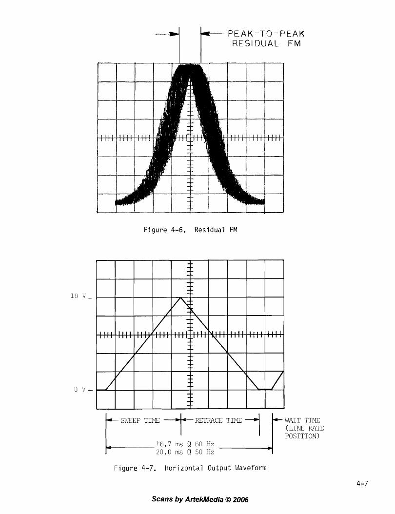
P E A K - T O - P E A K R E S I D U A L F M
SWEEP TIME --t RETRACE TIME 1 WAIT TIME ( LINE -RATE POSITION)
16.7 m s 9 60 Hz 20.0 rns @ 50 Hz
F i g u r e 4-7. Hor izon ta l Output Waveform
Scans by ArtekMedia O 2006

calibrate the display's sweep width to exactly 1 MHz and center the marker (for example, 500 MHz) on the display with the SWEEP TIME switch set to LIIVE. Read frequency drift directly from the scope display by noting the change in the marker's position with time. Each division represents 100 kHz. When reading drift over long periods of time, calibrate the display's sweep width to 5 MHz using 1 MHz harmonic markers. Next, turn off the 1 MHz markers and turn on the 10 MHz (or 50 MHz) harmonic markers. Center a marker on the scope display and read drift as before, except 1 division now equals 500 kHz.
The maximum allowable drift on bands 1 and 2 is 100 kHz per 5 minutes, or 2 MHz per 8 hours. This specification applies after a one-hour minimum warmup at a constant ambient temperature, and allowing a 5 minute stabilizing period after a frequency change. On band 3, the maximum allowable drift i s 200 kHz per 5 minutes, or 4 MHz per 8 hours.
4.7 BLANKING TEST
With the front-panel BLANKING switch turned on, the RF output in SIS and AF modes i s removed during the sweep retrace time to provide a zero-volt base line. Use the setup in Figure 4-1 and preset the controls as in Sections 4.2.1 or 4.2.2. The display should be as shown in Figure 4-2. Set the BLAlVKllVG switch to i t s up position, and verify that the zero-volt base line i s removed from the display. Repeat this test on bands 2 and 3. Reset the BLANKING switch to ON.
4.8 OUTPUT IMPEDANCE AND SWR TEST
A 50 ohm SWR bridge, a spectrum analyzer, and a signal generator are required for this test.
The output impedance and SWR of the Model 2002A are measured in combination, and the result i s expressed as return loss which may be directly converted to SWR. The Model 2002A and the signal generator, both operating in CW mode, are set to the same output level and test frequency. The system is calibrated with the test port of the SWR bridge open and a 0 dB return loss reference i s set on the spectrum analyzer. The Model 2002A is then connected to the test port of the SWR bridge. The SWR of the Model 2002A is obtained from the return loss indication on the spectrum analyzer as the signal generator is tuned through the test frequency range. The return loss indication i s disregarded at points where the two frequencies are exactly equal. The SWR should be less than 1.5:1 (return loss greater than 14 dB) with the Model 2002A OUTPUT STEP ATTENUATOR set to 0 dBm (10 dB insertion loss). The SWR should be less than 1.3: 1 (return loss greater than 7 dB) with the OUTPUT STEP ATTENUATOR set to -10 dBm (20 dB insertion loss).
4.9 RF OUTPUT MAXIMUM LEVEL TEST
This measurement i s made with a power meter. Set the power meter to its +15 dBm range. Set the Model 2002A controls as in Section 4.2.1, except set the MODE switch to CW. Connect the power sensor to the RF OUT connector of the Model 2002A. The power meter must read between +12.5 and +13.5 dBm. RF output flatness i s measured in Section 4.1 1.
4.10 RF OUTPUT ATTENUATION AND ACCURACY TESTS
4.10.1 STEP ATTENUATOR
The Step Attenuator provides 70 dB of attenuation in 10 dB steps. The accuracy can be measured by using a suitable attenuation test set, or by directly substituting precision RF attenuator pads for each 10 dB step of the Attenuator. The difference between the two outputs represents the Attenuator error. An RF detector can be used to recover the signal at levels down to approximately -40 dBm. Below this level, an RF amplifier or a sensitive receiver (spectrum analyzer) must be used. The allowable error i s +3% of the attenuation. The maximum error, which i s a t 70 dB, i s k2.1 dB. This error i s produced by the Step Attenuator alone, and does not include the flatness or the OUTPUT VERNIER ATTENUATOR error.
4.10.2 VERNIER ATTEIVUATOR
The accuracy of the OUTPUT VERNIER ATTENUATOR is measured using the power meter while operating the instrument in CW mode on band 1 at 250 MHz. With the OUTPUT STEP ATTENUATOR set to +10 dBm, adjust the VERNIER for a +3 dBm reading on the output METER. The power meter should read +13 k0.5 dBm. Using the OUTPUT VERNIER only, check the output METER readings in 1 dB steps between +3 and -10 dB. The power meter reading at each step should be within 0.5 dB of the indicated output level (the sum of the output METER reading and the OUTPUT STEP ATTENUATOR setting). The output i s not specified below -10 dBm output METER readings.
4.1 1 RF OUTPUT FLATNESS TEST
Flatness is the variation in output amplitude versus frequency. It i s normally measured with a power meter, but it can be measured with a broadband negative-polarity RF detector. The power meter method i s preferred, since its flatness i s better than most RF detectors. A power sensor i s used with the power meter, and a calibration chart is affixed to the sensor. At the operating frequency, a calibration factor noted on the chart i s set on the power meter's calibration factor control, and a corrected readitqg is
obtained from the power meter.
Scans by ArtekMedia O 2006

The flatness i s measured in the SIS mode with the SWEEP TlME switch set to MANUAL . The BAND switch i s set to 4, and the VARIMANUAL control i s adjusted through i t s range. The SLOPE control must be adjusted for zero slope. The power meter is set to i t s +15 dBm scale and connected to the RF OUT connector of the Model 2002A.
To read flatness down to the 1 MHz minimum, first calibrate the scope display from 0 to 10 MHz as follows. Set the SWEEP TlME selector to LlNE and set the START control to -10 MHz and the STOP control to +10 MHz. Turn off all markers and depress the EXT MARKER pushbutton to activate the 0 MHz marker. The 0 MHz marker should appear near the display center. Turn on the 10 MHz harmonic markers. Adjust the START control to position the 0 MHz marker on the left graticule borderline, and the STOP control to position the 10 MHz marker on the right graticule borderline. Turn off the EXT MARKER and turn on the 1 MHz harmonic markers. With the SWEEP TI ME selector set to MANUAL, adjust the VARIMANUAL control to position the zero beat of the 1 MHz marker approximately one division from the left borderline of the display graticule. Turn off the markers. Set the proper calibration factor and read the power meter. (The power meter will null i f the VARIMANUAL control is set to the zero beat of the 0 MHz marker.) Tune the 1 to 10 MHz range with the VARIMANUAL control and note the power meter readings.
Set the START and STOP controls to 10 and 2500 MHz respectively. Tune the entire frequency range with the VARIMANUAL control. Note the frequency where the maximum corrected power meter reading is obtained. Use the OUTPUT VERNIER to adjust the corrected output level to exactly +13 dBm a t that frequency where the maximum output level occurs. Again tune the full range and note the minimum corrected power meter reading. A minimum reading of a t least +12 dBm is required to meet the k0.5 dB flatness specification.
I f a detected swept response is to be observed, the lowest detected output level should be at least 90% of the highest detected level at sweep rates up to 100 MHzIms. At faster rates, the overall flatness may deteriorate slightly.
4.12 SWEEP TlME (HORIZONTAL OUTPUT) TEST
Connect the Model 2002A HORlZ OUT connector to the scope vertical input. Adjust the scope controls for an internally generated, automatic, line-triggered sweep of 2 mVIdivision, and a vertical sensitivity of 2 Vldivision. Set the Model 2002A BAND switch to 1, the SWEEP TIME selector to LINE, and the TRIGIR ECUR switch to R ECUR (full down position). Adjust the scope's vertical position, horizontal position, and trigger level to obtain a waveform as shown in Figure 4.7.
Set the SWEEP TlME selector to 0.1 - 0.01 sec and the VARIMANUAL control fully clockwise. The wait time should disappear and the sweep time should be less than 10 ms with approximately equal sweep time (rising) and retrace time (falling) periods. Set the scope time base to 20 msldivision. Adjust the VARIMANUAL control fully counterclockwise. The sweep time should be greater than 100 ms with approximately a 10:l ratio between the sweep and retrace time periods.
NOTE
The retrace time period remains fairly constant at any SWEEP TlME setting as the VARIMANUAL control varies the total sweep time period. With the VARIMANUAL control fully clockwise, the sweep and retrace times are both 0.01 seconds. With the control fully counter- clockwise, the sweep time is approximately 0.1 seconds and the retrace time remains 0.01 seconds. On the next lower range (1 - .I 1, the retrace time should be a constant 0.1 seconds, and the sweep time should vary from 0.1 to 1 second.
Repeat the previous checks for the 1 - .I, 10 - 1, and 100 -10 second positions on the SWEEP TlME selector switch. Adjust the scope time base as necessary to ensure that the VARIMANUAL control will adjust the sweep time from greater than the maximum to less than the minimum time specified for each range.
Set the SWEEP TlME selector to MANUAL and adjust the VARIIVIANUAL control throughout i t s range. A DC voltage should be present a t the HORlZ OUT connector that is variable from 0 k0.5 V with the control fully counterclockwise to +10 k0.5 V with the control fully clockwise. Use a DVM for this measurement.
Set the SWEEP TlME selector to the .1 -.01 position and the TRIGIRECUR switch to i t s middle position. The sweep should be disabled. Moving the TRIGIRECUR switch to the full up (spring-loaded) position and then releasing it should produce one complete sweep cycle.
NOTE
The triggered mode of operation is possible only in the variable rate positions, and will not operate in the LlNE or MANUAL positions of the SWEEP TlME selector.
4.13 MARKER SYSTEM TESTS
The Model 2002A utilizes a birdy-bypass marker system which provides for both internal and external markers. A CW signal generator i s used to check out the external system. Option A3, which provides a combination of 1, 10, 50, and 100 MHz harmonic markers, i s required to fully check out the internal marker system.
Scans by ArtekMedia O 2006

A front-panel rotary switch (labeled HARMONIC MARKERS) selects the desired comb in Option A3. An internal operator control on module MI05 (labeled Size Ratio) adjusts the ratio of small to full-size markers in the comb to facilitate identification in all marker options. Other markers, Options A1 and A2, i f installed, and the external marker, are individually selected by label from the row of seven front-panel MARKER pushbutton switches. All marker geometries (size, width, tilt, and rectification) are controlled from front-panel switches and controls. In addition, all markers have internal Size controls (see Section 5.3.6 for adjustment procedure).
4.13.1 EXTERNAL MARKER
Use the setup in Figure 4-1 and connect the CW output of a signal generator to the Model 2002A MARKER IN connector. Set controls as in Section 4.2.3, and adjust the MARKER SIZE control to obtain a display similar to Figure 4-2. Set the signal generator for a 100 mV CW output, and depress the Model 2002A EXT MARKER pushbutton. Tune the signal generator from 1 to 500 MHz and note the movement of the external birdy in the display. The fundamental external birdy amplitude should be approximately equal to the amplitude of the even harmonic markers in the comb. The amplitude of second and thrid harmonics of the external signal, when in the band, may also be approximately equal to the fundamental marker amplitude.
When operating on band 2 or 3, the second, third, or higher harmonics of the external signal generator carrier may be required to verify operation of the external marker system on signal generators with limited maximum frequency. Increasing the level of the carrier may be required.
4.13.2 SllVGLE FREQUEIVCY MARKER (OPTIOIV A l )
Use the procedure in the previous sections, and depress the correct pushbutton for the single frequency marker to be tested. Turn off all other markers, and set the BAND switch for the correct band to display the single frequency marker. Adjust the CENT FREQ control to center the marker on the display, and read the FREQUENCY SCALE to identify the marker within 5 MHz.
4.13.3 INDIVIDUAL HARMONIC MARKERS (OPTION A2)
Option A2 provides a harmonic marker comb up to 1500 MHz. Use the setup and procedure in Section 4.2.3, except depress the appropriate pushbutton in the row of MARKER switches (50 HAR, for example), and turn off all other markers.
The Option A2 markers can be tested using a procedure similar to Section 4.13.4, except the maximum operating frequency i s 1500 NlHz for the individual harmonic markers.
4.13.4 DELUXE HARMONIC MARKERS (OPTION A3)
The Option A3 harmonic markers are used in several previous performance tests. The 1, 10, 50, and 100 MHz harmonic (comb) markers are controlled by the front-panel HARMONIC MARKERS rotary switch. To check out the Option A3 markers, proceed as follows.
NOTE
The following tests for marker frequency accuracy, marker width, size, rectification and tilt are made with the 50 MHz harmonic markers. Other markers can be tested using a similar procedure.
MARKER ACCURACY
Marker accuracy can be verified by any one of several methods. In one method, a frequency counter measures the RF output frequency of the Model 2002A as follows: A convenient harmonic marker (preferably near the counter's maximum frequency) or a single frequency marker i s displayed on the scope with the Model 2002A operating in AF mode with a sweep width of approximately 1 MHz. The sweer, time is then set to IVANUAL, and the VARIMANUAL control i s adjusted for a zero beat of the displayed marker. The marker's frequency i s read on the frequency counter, For example, a 500 MHz marker should read 500 MHz +25 kHz. The allowable error i s as follows: 0.005% at 2 5 " ~ and 0.007% at 0 to 5 0 " ~ for Options A1 and A2. For Option A3, the allowable error i s 0.005% at 0 to 5 0 " ~ . Since the error i s quite small, a higher harmonic frequency provides an error which i s more easily read on the counter. On Option A3, a single crystal reference i s used for all harmonic frequencies, and only a single measurement i s required.
A second method uses a tunable frequency synthesizer as an external marker. With the Model 2002A operating in AF mode, a tes t marker i s displayed at 1 MHz sweep width. The synthesizer i s tuned until i t s zero beat coincides in the scope display with the zero beat of the test marker.
A third method uses a frequency counter only, but requires removal of the instrument and marker covers. A probe from the marker oscillator section to the counter i s adjusted for a signal level sufficient for the counter to accurately read the crystal frequency.
Scans by ArtekMedia O 2006

The highest crystal frequency used in the Model 2002A i s 50 MHz. Markers above 50 MHz use harmonics of a given crystal frequency.
Test equipment for marker accuracy i s not listed in Table 4-1, since the inherent stability of quartz crystals makes a marker accuracy check unnecessary in all but the most critical applications.
MARKER WIDTH
Repeat the setup in Figure 4-1, and set the Model 2002A controls to position a 2500 MHz marker on the display at a sweep width of exactly 1 MHz. Other controls should be initially set as in Section 4.2.1. Adjust the MARKER SlZE control and scope vertical sensitivity for a 2 Vpp marker display.
Adjust the CENT FREQ control to center the marker's zero beat on the scope display. With the MARKER WIDTH switch set to WIDE, note that the displayed marker width is approximately 400 kHz (each horizontal division equals 100 kHz). Decrease MARKER WIDTH in successive steps to NARROW, and note that the marker width decreases in steps to approximately 15 kHz at IVAR ROW.
NOTE
Marker width i s also a function of internal marker Size controls. The above check applies to normal settings of internal marker controls.
approximately 10 mVpp at the counterclockwise limit. Set the SlZE paddle switch to mid-position (small diamond). Again rotate the MARKER SlZE control throughout i t s range. The displayed marker amplitude should vary from approximately 25 mVpp to approximately 50 pVpp.
MARKER RECTIFICATION
Set the SlZE paddle switch to full up position (triangle). This position provides positive retified birdy markers for use with X-Y plotters. With the SWEEP TIME selector set to .1 - .01, adjust the VARIMANUAL control fully counterclockwise. Disconnect the R F detector from the DEMOD IN connector on the Model 2002A and rotate the MARKER SlZE control throughout its range. With the scope properly adjusted, the marker amplitude should vary from approximately 2 V to 1 mV. The rectified marker amplitude depends upon the RF detector impedance when connected to the DEMOD IN connector. With the DEMOD IN connector center conductor shorted to ground, the voltages should vary from approximately 0.2 V to 1 mV.
MARKER TILT
Center the 2500 NlHz marker in the display at a sweep width of approximately 200 MHz. Set the TILT/IVORM switch to TILT and the SlZE paddle switch to full down position. While adjusting the MARKER SlZE control throughout its range, note that the marker i s adjustable from a 4 Vpp nearly vertical marker to a horizontal marker equal to approximately 10% of the horizontal display (1 division of 10).
MARKER SlZE 4.14 EXTERNAL PROGRAMMING
Set Model 2002A controls as in Section 4.3.2, and observe the 50 MHz marker comb from 50 to 500 MHz. Note that even harmonic markers (100, 200, . . . etc.) have a uniform amplitude in the display. The odd harmonic markers (50, 150, . . . etc.) have a smaller, but uniform amplitude. The relative amplitude or size i s determined by the internal Size Ratio control (see Section 5.3.5). The even harmonic of the 50 MHz harmonic markers should be of uniform amplitude throughout all four bands. The odd harmonics should be smaller, but of uniform amplitude throughout all bands.
Set the MODE switch to AF and center the 2500 MHz marker on the display at a sweep width of approximately 2 MHz using the CENT FREQ and SWEEP WIDTH controls on band 3. Set the scope's vertical sensitivity and position controls as required to read marker amplitude in the following steps. With the front-panel SlZE paddle switch fully depressed (to the large diamond), rotate the MARKER SlZE control throughout i t s range. The displayed marker amplitude should vary from approximately 4 Vpp at the clockwise limit to
External programming inputs are not normally checked at incoming inspection unless these special functions are to used in a particular application. The program input signals, external controls necessary, and input pin connections are covered in Section 2, Operation. If it i s necessary to check these functions at incoming inspection, reference can be made to that section of the manual for complete setup instructions.
4.15 SLOPE TEST
Set the BAND switch to 4, the MODE switch to SIS, and the START and STOP controls to 1 and 2500 NIHz, respectively. Use the OUTPUT VERA1 I ER to calibrate levels of 7.5, +lo, and +12.5 dBm on the scope display (refer to Figure 4-7). Reset the OUTPUT VERIVI ER for a +10 dBm output (0 dBm on output METER). Use a screwdriver to adjust the front-panel SLOPE control fully clockwise. When viewed on the scope display, the output at 2500 MHz should be approximately +12.5 dBm and the output at 1 MHz should still be +10 dBm. Adjust the
Scans by ArtekMedia O 2006

SLOPE control fully counterclockwise. The output at 2500 MHz should be approximately +7.5 dBm and the output at 1 MHz should still be +I0 dBm when viewed on the display. The sloped line should be approximately linear.
4.16 1 KHZ MODLILATION TEST
Set the BAND switch to 4, the MODE switch to S/S, the START control to 1 MHz, the STOP control to 2500 MHz, the SWEEP TlME selector to MANUAL, and the VARI MANUAL control fully ccw. Turn off all markers and blanking. Turn the 1 kHz MOD pushbutton switch on and set the scope for 0.2 msec/division on the horizontal time base, internally triggered. A waveform (approximately square) with a period of 1 msec should be displayed. The
amplitude of the waveform should be equal to that of the unmodulated waveform. Tune the VARIMANUAL control throughout i t s range and note the amplitude of the waveform at all frequencies. Turn the 1 kHz MOD switch off.
4.17 PEN L l FT (OPTION B4)
Two terminals are provided on the rear panel which provide contact closure during forward sweep time. Pen l i f t occurs only in the 1 - 10 and 10 - 100 positions of the SWEEP TlME control. The unit i s tested with an X-Y plotter or with a VOM to indicate contact closure during the sweep trace interval. The marker SIZE paddle switch should be in i t s full up position when checking markers with an X-Y plotter;
Scans by ArtekMedia O 2006

SECTION 3
5.1 INTRODUCTION
This section provides information for servicing, calibrating, and troubleshooting the Model 2002A Sweep/Signal Gen- erator.
5.2 SERVICE INFORMATION
5.2.1 DISASSEMBLY INFORMATION
Refer to Figure 5-1.
REMOVAL OF BOTTOM COVER - Remove two rear feet (A) and l i f t cover off with a slight rear movement. Reinstall cover by reversing the removal procedure.
REMOVAL OF TOP COVER - Remove the single screw (B) from top and l i f t off cover with a slight rear movement. Reinstall cover by reversing the removal procedure.
REMOVAL OF SIDE PANEL - To remove the right side panel, refer to Section 5.2.3. To remove the left-side panel, remove the six screws (E) holding the side panel to the instrument. However, one side panel must remain on the instrument to secure the front-panel assembly to the chassis.
CAUTION
To prevent possible damage to harness when reinstalling side panels, use only the original screws or equivalent. Longer screws in the bottom two holes can cause damage to wiring.
5.2.2 MODULE SERVICING
REMOVAL OF MODULE - Modules may be replaced by removiqg any cables attached to top of the modules and
MAINTENANCE
removing hold-down screw (C) from bottom. Rock module slightly while lifting upward to free module from chassis socket.
REMOVAL OF MODULE COVER - Remove all nuts and screws from top of module and slide cover off.
REINSTALLING MODULE - Before installing the module, check that module pins are straight and properly aligned; then carefully seat module pins into the chassis socket, replace module hold-down screw (C) to insure a good ground connection between module and chassis, and replace any cables attached to top of module. Module cable connections are shown in Figure 5-22.
NOTE
If a defective module is replaced with a new module, certain calibration procedures must be repeated as shown in the following l i s t :
MODULE PROCEDURE
MlOlB M102A M103A M104A MI05 MI09 MI10 MA1 I I M I 21 M I 31 MI32 M6C M6H
M6S MI06
Sweep Rate Frequency Cal Frequency Cal Level Cal None Frequency Cal Frequency Cal Level Cal 1 kHz Mod Adj Frequency Cal None None Marker Size Marker Size Marker Size
SECTION
Scans by ArtekMeda O 2006
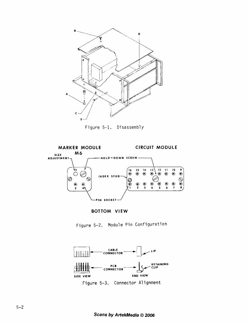
SIZE ADJUSTM
ARKER MODU M 6
L E CIRCUIT MODULE
- H O L D - D O W N SCREW 7 I N D E X STUD- @
P I N SOCKET J
BOTTOM VlEW
Figure 5-2. Module Pin Configuration
CABLE CONNECTOR -C 'Ip
* PCB RETAIN ING
CONNECTOR
SIDE V IEW END V I E W
Figure 5-3. Connector Alignment
Scans by ArtekMedia O 2006

SERVICE KIT KO05 - This kit contains a module extender, RF extension cables, and adapters which enable a module to be electrically operated while physically located above the rest of the modules, thereby making all parts easily accessible.
MODULE-PIIV NUMBERING SYSTEM - The module pins are numbered as shown in Figure 5-2. The off-center index stud prevents the module's being plugged in backward and also provides a method for locating pin 1.
NOTE
All 16 pins are not required in each module. Only the pins actually used are installed, but the numbering system remains the same.
5.2.3 OUTPUT AMPLIFIER SERVICING (MA1 11)
Refer to Figure 5-22. First remove cable W2 from the Amplifier and the M l l O Sweep Oscillator. Remove the sweep sample cable, W5, from the Amplifier, and remove the output cable W3 from the Step Attenuator. (Do not attempt to remove cable W3 from the Amplifier yet.) Next, remove the 6 screws holding the right-side panel to the instrument (screws (E) in Figure 5-1). Do not remove the two screws in the side panel holding the Amplifier to the side panel. The right-side panel can now be removed from the instrument, which will provide access to the Amplifier. The Amplifier can be operated in this position by substituting for cable W2 with a longer flexible cable provided in the service kit. Remove cable W3 from the Amplifier output and connect an R F detector or power meter directly to the Amplfifier output to check i t s performance. To reinstall the Amplifier, reverse this procedure. Remember to securely tighten cable W3 to the Amplifier output before reinstalling the side panel.
5.2.4 POWER SUPPLY SERVICING
PRINTED CIRCUIT BOARD CONNECTORS - When re- installing a harness connector to the Power Supply printed- circuit board, be sure connector i s properly aligned with the board connector pins and that connector faces proper direction (see Figure 5-3).
POWER SUPPLY BOARD REMOVAL - The Power Supply board and heatsink can be removed by removing the four screws which secure the printed circuit board to the instru- ment rear panel. After removal of the connecting harnesses, the board can be carefully lifted from the in- strument.
CAUTlOlU
The Power Supply board may be raised far enough to allow
checking of many components with the harnesses s t i l l connected; however, power must NOT be applied to the instrument unless the negative (ground) side of C10 i s connected to the instrument chassis ground and to the positive (ground) side of C9 (jumper wires are sufficient).
The Power Supply board i s reinstalled by reversing the removal procedure.
5.2.5 TRANSISTOR AND IC LEAD CONFIGURATION
Lead configuration i s shown in Figure 5-4.
5.2.6 RECOMMENDED TEST EQUIPMENT
The tes t equipment shown in Table 4-1 i s recommended for servicing, troubleshooting and calibrating the Wavetek Model 2002A.
5.3 CALIBRATION PROCEDURE
The following procedure assumes the instrument i s equipped with the A3 Deluxe Harmonic Marker option. Calibration by using an external marker generator and other marker options i s possible; however, a complete calibration by this method i s extremely inefficient.
Figure 5-4. Component Lead Configuration
Remove top and bottom covers. The instrument i s calibrated using the module extender from the service kit. Allow a half-hour warm-up before calibrating.
In general, calibration should be performed in the sequence given.
5.3.1 POWER SUPPLY CHECK AND ADJUSTMENT
The Power Supply provides +27 VDC (unregulated), and three regulated DC voltages, +18 V, -1 8 V, and +7 V to the instrument. The performance of the Power Supply can conveniently be checked by measuring the values a t J2. (See Figure 5-22 and Table 5-1 .)
The Power Supply also supplies a 20 VAC signal on pin 8 of J2 which i s used to trigger the sweep rate circuit when the SWEEP TIME control i s set to LINE.
A separate +20 V supply is used to the supply DC voltage to the MA1 11 Output Amplifier. I t i s located on the under side of the chassis as shown in Figure 5-23.
Adjust the +20 volt control to provide +20.0 volts a t the indicated point in Figure 5-23. Typical peak-to-peak ripple is <10 mV.
Scans by ArtekMedia O 2006

MA I NTENANCE
D S G or
S D G
OUT
+ v-
oF NULL F S E T d T b N C
F i g u r e 5-4.
E C B
CURRENT LIMIT
CURRENT
INVERTING INPUT
NON-INV INPUT
REF OUT
O F F S E T h v + NULL
Component Lead C o n f i g u r a t i o n
GNO
Scans by ArtekMedia O 2006

TABLE 5-1. J2 PIN VALUES WAIT TIME ADJUSTMENT
J2 VOLTAGE & TYPICAL PEAK- PIN SUPPLY TOLERANCE TO-PEAK RIPPLE
2 & 3 +18 +18.00 ADJ .5 mV
4 & 5 -18 -1 8.00 ADJ .5 mV
9 COMMON COMlVlON - - - - - - - -
*With input 11 5 VAC
5.3.2 SWEEP RATE ADJUSTNIEIVT AND CHECKS
The sweep rate circuit consists of module MlOlB and associated front-panel controls. I t provides the basic ramp from which the horizontal output and sweep drive signals are derived, plus the RF blanking signal and a precision + I 0 V supply. The following procedure checks and calibrates the sweep rate circuit.
DISASSENIBLY PROCEDURE
Remove the screw from the top of module MlOl B and l i f t cover off. Figure 5-5 shows the location of the MlOlB adjustments. Figure 5-6 shown the associated front-panel controls.
FREQ ADJUSTMENTS
Set the instrument control as follows:
MODE AF BAND 1 SWEEPTIME .01 - .1 VARIMANUAL full cw TRIGIRECUR RECUR BLAIVKIIVG ON SWEEP DWELL OFF
Connect the oscilloscope's vertical input to the HOR l Z OUT connector on the instrument front panel. Adjust the oscilloscope's sensitivity, position, and time base controls to produce a stable pattern similar to Figure 5-7. Adjust the Freq adjustment in the MlOlB module to produce a sweep time of <I0 msec. Set the MANUAL control fully counterclockwise and check the sweep time. It must be longer than 110 msec.
Set the instrument controls as follows:
MODE BAND SWEEP TIME VARIMANUAL TRIGIRECUR BLANKING SWEEP DWELL CENT FREQ SWEEP WIDTH
AF 2 LIIVE N /A RECUR ON OFF 1000 MHz 500 MHz
The scope should show a triangle wave with a delay of approximately 1 msec in approximately the center of both the rise and fall of the waveform (see Figure 5-7). These delays are due to band switching discontinuities. Adjust the Wait control (located on the rear of the SWEEP TIME switch - see Figure 5-22) to produce a 1 msec delay at the bottom of the triangle (see Figure 5-8).
Set the BAND switch to 1. The wait time at the bottom of the triangle should be approximately 3 msec with no delays due to band switching discontinuites. The same should be true when the BAND switch i s set to 3.
Set the BAND switch to 4. The rise and fall times of the triangle should be approximately twice as long as they were on Band 2, thus the repetition rate is half the line frequency. The wait time should vary from approximately 1 to 7 msec, depending upon the number of band switching discountinuity delays present as the CENT FREQ and SWEEP WIDTH control settings are varied.
MANUAL LIIVl IT ADJUSTMENT
Set the front-panel SWEEP TINIE selector to its MANUAL POSITION. Set the scope's horizontal trigger control for line rate. Set the VARIMANUAL control fully clockwise and adjust the Manual Limit control on the M101B to produce a DC voltage exactly equal to the peak amplitude of the horizontal output as read in Figure 5-7 or 5-8 (approximately +10 V).
SWEEP DWELL
Set the BAND switch to 4 and turn the rear-panel SWEEP DWELL switch on. The wait time at the bottom of the triangle should increase by approximately 4 msec. The fall time of the triangle wave should decrease, thus the repetition rate of the sweep remains at half the line frequency.
Set the BAND switch to 1, 2, or 3. The rise and fall times of the triangle wave should be the same as they were
Scans by ArtekMedia O 2006
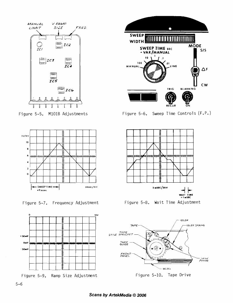
7 F i g u r e 5-5. MlOlB Ad jus tmen ts
F i g u r e 5-7. Frequency Ad jus tmen t
+ 5 0 n v
O n V
- 5 0 n V
SWEEP
WIDTH
SWEEP T l M E S E C MODE
VAR~MANUAL I
L I N E
U c w T R I G BLANKING
Y Y R E C U R 0 P4
F i g u r e 5-6. Sweep Time C o n t r o l s (F.P.)
WAIT T l M E = I mSEC
F i g u r e 5-8. W a i t Time Ad jus tmen t
0 inv
TAPE -\
F i g u r e 5-9. Ramp S i z e Ad jus tmen t
IDLER
-- ' - - B E Z E L
F i g u r e 5-10. Tape D r i v e
Scans by ArtekMedia O 2006

previously, but the wait time will increase by approximately 4 msec, thus cutting the repetition rate in half due to the wait time overlapping the line trigger pulse.
PREClSlOlV k10 V SUPPLY CHECK
In order to maintain the accuracy of the FREQUENCY SCALE in the SIS, AF and CW modes of operation, the + I0 V supplies, the standard-sweep ramp, and the inverted sweep ramp must maintain precise relationships with each other. These relationships are maintained by precision resistors and a single potentiometer (V Ramp Size) located in the MlOl B module. The following procedure checks these relationships and provides a high-resolution method of calibrating the inverted ramp size.
Connect the DVM to pin 7 of the MI31 module. Set the BAND switch to 1, the MODE switch to CW, and the CENTER FREQ control against i t s mechinical stop a t the low end of the FREOUENCY SCALE. Record the voltage read on the DVM to three decimal places. Set the CENTER F REQ control against i t s mechanical stop a t the high end of the FREQUENCY SCALE. Compare this voltage (ignoring polarity) to the previously read voltage. The difference should be less than 10 mV.
INVERTED RAMP SlZE (V RAMP SIZE)
Remove the vertical input to the oscilloscope. Set the SWEEP TlME to MANUAL. Adjust the VARIMANUAL sweep time control to position the dot to the exact center of the oscilloscope display. Set the MODE switch to CW and both CENT FREQ and SWEEP WIDTH controls against their mechanical stops a t the high end of the FREQUENCY SCALE.
Connect the DVM to pin 7 of the MI31 module and record the voltage to three decimal places. Set the MODE switch to SIS and compare the DVM reading to the previously recorded voltage. The difference should be less than 35 mV. Record the second voltage to three decimal places. Rotate the VARI MANUAL control to i t s extreme counterclockwise position. Adjust the V Ramp Size control in module MlOl B (see Figure 5-5) to obtain the same exact voltage. Rotating the VARIMANUAL control through i t s entire range should not change the DVM reading. Replace the cover on the M 10.1 B module.
This procedure ensures the frequency error produced by module MlOl B will be less than 3 MHz.
5.3.3 FREOUENCY ADJUSTMENT RAMP SlZE CHECK
Set the instrument controls as follows:
BAND 1 SWEEP TIME LINE MODE AF CENTER FREQ and SWEEP WIDTH controls set against their mechanical stops a t the high end of the FREOUENCY SCALE.
Connect the instrument HORlZ OUT connector to the oscilloscope's horizontal input. Adjust the oscilloscope to operate in an X-Y mode with i t s horizontal sensititity set to 1 volt per division and the vertial sensitivity set to 50 millivolts per division. Center the trace on the scope with the position controls as shown in the dashed line of Figure 5-9. Connect the oscilloscope's vertical input to pin 7 of the MI31 module. Set the SWEEP TINIE selector to the 1 - 10 sec position and the VAR MANUAL control fully clockwise. (This slow sweep is necessary to prevent scope errors due to overdriving.) A trace with a repetition rate of 1 second should appear at the left side of the scope display (see Figure 5-9). The end of the scope trace should be 0 volts k70 mV measured on the vertical axis. Do not change the setting of the SWEEP WI D-rH control, but set the CENT FREQ control against i t s mechanical stop at the low frequency end of the FREOUENCY SCALE. The end of the scope trace should now be a t the right side of the display (Figure 5-9) and again have an amplitude of 0 V +70 mV.
MECHANICAL ADJUSTMENT OF FREQUEIVCY INDICATOR TAPE
Rotate both START and STOP thumbwheels to their lowest frequency positions a t the mechanical stops. Both frequency indicators must read 0 MHz k2 MHz when read on the Sweep Width FREOUENCY SCALE: i f not, proceed as follows: With reference to Figure 5-1 0, disengage ldler by forcing ldler Spring to a disengaged position. While ldler i s disengaged, rotate the Tape Drive Gear until the frequency indicator indicates zero frequency. Release the ldler Spring and engage the Idler. If the frequency error is still more than 2 MHz, loosen the screw holding the Tape Guide and Rotate the Guide so the Tape can be disengaged from the sprockets on the Tape Drive Gear. Disengage the Tape from the Tape Drive Gear sprockets and advance the tape one sprocket in the opposite direction of the frequency error. Engage the Tape on the sprocket, reposition the Tape Guide and tighten the screw. Again disengage the ldler and turn the Tape Drive Gear to indicate zero frequency. The front-panel CENT FREQISTART control thumbwheel must be held against i t s mechanical stop during the entire adjustment procedure.
OSCl LLOSCOPE LINEARITY CHECK
Before making the following electrical adjustment, first check the horizontal linearity of the oscilloscope, since any oscilloscope linearity errors will be added to the linearity adjustment error.
5-7
Scans by ArtekMedia O 2006

MA1 NTENANCE
LIN ADJ
O ~ y D [
2 0 0 M H z 2 5 0 M H z M A R K E R M A R K E R
F i g u r e 5-11. Scope L i n e a r i t y Check
BAND 3
LIN ADJ
L .I
TEST TEST
POINT POINT
A 0
( LIN ADJ
CENTERING SWEEP BAND WIDTH
3 26 2A 1 2A 26
F i g u r e 5-12. Sweep D r i v e Adjustments
BAND 2 B
LIN ADJ
Scans by ArtekMedia O 2006

Adjust the oscilloscope to operate in an X-Y mode and set the horizontal and vertical sensitivities to 1 Vldivision. Connect the instrument HOR lZ OUT connector to the oscilloscope's horizontal input, and the VERT OUT connector to the oscilloscope's vertical input. The scope inputs should be DC coupled.
Set the instrument controls as follows:
BAND 1 MODE AF CENT FREQ 250 MHz SWEEP WIDTH 100 MHz SWEEP TIME LINE HARMONIC MARKERS 50 MHz
Adjust the oscilloscope's horizontal position and sensitivity controls for a horizontal line that over-travels the scope graticule approximately 0.5 division on both ends (see Figure 5-1 1). Adjust the MARKER WIDTH for a display width that slightly overlaps the width of a graticule line. Fine adjust the CENT FREQ and SWEEP WIDTH controls until the 200 MHz marker exactly coincides with the extreme left graticule line and the 250 MHz marker exactly coincides with the center line of the scope graticule as shown in Figure 5-1 1. Disregard the position of the 300 MHz marker. Adjust only the CENT FREQ control until the 200 MHz marker coincides with the graticule line one division from the extreme left. The 250 MHz marker should coincide with the first graticule line to the right of center within k.25 minor division. Continue to adjust only the CENT FREQ control to position markers at one division intervals until the 200 MHz marker coincides with the graticule center line.
The 250 MHz marker should coincide with i t s corresponding graticule line within k0.25 minor divisions at all five check points across the display.
The 0.25 minor division error (50 mV) is equivalent to a 0.5% linearity error. This error can be eliminated by using the same scope for calibration and operation.
ELECTRICAL FREQUENCY ADJUSTMENTS
Electrical frequency adjustments are located in modules M 131, M 102A and M 103A. In order to access the controls in these modules, the module being adjusted should be set up on a module entender (part of Service Kit K004) with the module cover removed.
LINEARITY REFERENCE ADJUSTMENT
Set the instrument controls as follows:
BAND MODE CENT FREQ
1 AF exact1 y 250 NlHz
SWEEP WIDTH SWEEP TlME
exactly 500 MHz LlNE
Adjust the oscilloscope to operate in an X-Y mode and set the horizontal and vertical sensitivities to 1 Vldivision. Connect the instrument HORlZ OUT connector to the oscilloscope's horizontal input and position the trace as shown in Figure 5-1 3. The scope trace must be exactly 10 divisions long, starting exactly on the extreme left graticule line and ending exactly on the extreme right graticule line. Adjust the oscilloscope's horizontal sensitivity and position controls as necessary. Connect the oscilloscope's vertica! input to Test Point A (see Figure 5-1 2) of module M 102A.
Adjust the + Lin Ref Control to position the "knee" exactly one division from the extreme right side of the display (see Figure 5-1 3). Next, connect the oscilloscope's vertical input to Test Point B and adjust the - Lin Ref control to position the "knee" exactly one division from the extreme left side of the display (see Figure 5-1 3).
CENTER FREQUENCY ADJUSTMENT
Set the instrument controls as follows:
BAND MODE CENT FREQ SWEEP WIDTH SWEEP TlME HARMONIC MARKERS
1 AF exactly 250 MHz 10 MHz LlNE 50 MHz
Adjust the oscilloscope to operate in an X-Y mode and set the horizontal and vertical sensitivities to 1 Vldivision. Connect the instrument HORlZ OUT connector to the oscilloscope's horizontal input and center the horizontal trace on the scope.
Connect the instrument's VERT OUT connector to the oscilloscope~s vertical input and adjust the MARKER SIZE and WIDTH controls for a display similar to that shown in Figure 5-14. I f no marker i s visible on the display, increase the SWEEP WIDTH control until a small marker i s present on the display. (-The operation is such that odd harmonics of 50 MHz will have a smaller amplitude than even harmonics. Since the center frequencies of bands 1, 2A, and 2B are odd harmonics, they will have a smaller amplitude, while the center frequency of band 3 is an even harmonic and will have a larger marker amplitude.) This procedure will work i f the center frequency error i s less than 100 MHz. I f the center frequency error i s more than 100 MHz, an external marker must be used to identify the correct 50 NlHz harmonic. The external marker generator's frequency can be at the center frequency or at a subharmonic. For example, the band 3 center frequency is 2000 MHz, so the external marker frequency can be 2000, 1000, or 500 MHz. The external marker circuit will produce harmonics of the input signal to 2000 MHz.
5-9
Scans by ArtekMedia O 2006

F i g u r e 5-13.
L j n e a r i t y Reference
Ad jus tmen t
F i g u r e 5-14.
Cen te r i ng
F i g u r e 5-15. D i s p l a y Cal i b r a t i o n
2 5 0 M H z MARKER
Scans by ArtekMedia O 2006

CENTERING BAND 1
With the M103A Centering Band 1 control (see Figure 5-12) adjust the 250 MHz marker to the center of the display as shown in Figure 5-1 4. Decrease the sweep width to <10 MHz before completing the adjustment.
CENTERING BAND 2
This will be covered in the Linearity Adjustment (Band 2) Section below.
CENTERING BAND 3
Set the BAND switch to 3 and center the 2000 MHz marker on the display with the Centering Band 3 control. Without touching other controls, switch between bands 1 and 3 and verify that each marker i s centered.
ADJUSTMENT OF 0 MHz LOCK-IN POIIVT
Set the instrument controls as follows:
BAND MODE CENT FREQ SWEEP WIDTH
1 AF 0 MHz 10 MHz
Adjust the M102A Sweep Width Band 1 control (see Figure 5-12) to position the 0 MHz lock-in point to the exact center of the display.
Set the instrument controls as follows:
BAND MODE CENT FREQ SWEEP WIDTH SWEEP TIME HARMONIC MARKER
1 AF exactly 250 NlHz 530 MHz LINE 50 MHz
With the oscilloscope's horizontal position and sensitivity controls, superimpose the 0 MHz lock-in point exactly on the extreme left graticule line and the 250 MHz marker exactly on the center line of the scope graticule. (Disregard location of all other markers.) See Figure 5-15.
LINEARITY ADJUSTMENT (BANDS 1 AND 3)
Being careful not to disturb the oscilloscope's position and sensitivity controls, readjust the M 102A Sweep Width Band 1 control to superimpose the 150 MHz marker exactly on the scope graticule line as shown in Figure 5-1 6. Proceed to adjust Band 1 Lin 1 through 9 controls in Module M102A
(Figure 5-12) to position each marker as'shown in Figure 5-16. (There is no Lin 6 control for Band 1.) The adjustment procedure must be done in the sequence given.
Each of the eleven markers in the display must be aligned within k.1 full division of i t s vertical graticule line to provide the maximum specified linearity error of 1%.
Set the MODE switch to S/S and adjust the START and STOP controls to exactly duplicate the display shown in Figure 5-1 6.
Change to band 3.
Turn on the 100 MHz markers. Check the position of the 2000 MHz marker. Adjust the Sweep Width Band 3 and Linearity controls (Lin 1 through 9) to position the markers as shown in Figure 5-16. (Use the Sweep Width Band 3 control to set the 1900 MHz marker.)
While observing the oscilloscope display, switch between bands 1 and 3 without adjusting any other controls. There should be a negligible shift in marker location on the display.
Set the oscilloscope's vertical sensitivity control for 5 V/ division and connect the oscilloscope's vertical input to pin 7 of the M 131 module.
LINEARITY ADJUSTMENT (BAND 2)
Set the BAND switch to 2. With the oscilloscope's vertical input s t i l l connected to pin 7 of the MI31 module, adjust R36 in the MI31 to position the band 2A portion of the ramp such that it crosses 0 V exactly 2.5 divisions in from the extreme left graticule (see Figure 5-17). Adjust R42 such that the band 2B portion crosses 0 V exactly 2.5 divisions in from the extreme right graticule. Turn on the 50 MHz markers and connect the oscilloscope's vertical input to the instrument's SCOPE VERT connector. Using the M 103A Cent 2A control, position the 750 MHz marker exactly 2.5 divisions in from the extreme left graticule. Using the Sweep Width 2A control, position the 700 MHz marker exactly 2 divisions in from the extreme left graticule. Adjust the Band 2A Lin Adj controls to position the other markers at 0.5 division intervals (see Table 5-2).
Using the M103A Cent 2B control, position the 1250 MHz marker exactly 2.5 divisions in from the extreme right graticule. Usirrg the Sweep Width 2B control, position the 1200 MHz marker exactly 3 divisions in from the extreme right graticule. Adjust the Band 2B Lin Adj controls to position the other markers at 0.5 division intervals (see Table 5-2 and Figure 5-1 7).
Scans by ArtekMedia O 2006

F i g u r e 5-16. L i n e a r i t y Adjust i i ients,
Bands 1 And 3
B A N
F i g u r e 5-17. L i n e a r i t y Adjustments,
Band 2
B A N D 3 1.5 1 . 7 1.9 2 . 1 2 . 3 2 . 5 GHz
F i g u r e 5-18. L i n e a r i t y Adjustments,
Band 4
B A N D 4 2 750 1250 2 0 0 0 2 5 0 0 MHz
Scans by ArtekMedia O 2006

TABLE 5.2. BAND 2 LINEARITY ADJUSTMENT now be centered in their respective positions.
(Adjust controls in order given.)
BAIVD A BAND B
CTL MKR (MHz) CTL MKR (MHz)
Replace the covers on modules M 102A and IV1103A.
BAND 4 SET-UP
Set up of band 4 i s a special case since this is a stacked band made up of four individual oscillators which have already been se t up for linearity.
All controls for setting up band 4 are located in module MI31 (see Figure 5-19). These controls act to break the basic ramp from the M I 0'1 B rate generator into 4 sequential 10 V ramps before it i s applied to the shaping circuits.
Place the front-panel BAND switch to 4, leaving the other front-panel controls and scope settings as they were for the Band 3 linearity adjustments. Using R57 in the M131, set the first crossover point approximately 2 divisions in from the extreme left graticule. Use R60 to set the second crossover 4 divisions in from the extreme left graticule and R64 to set the last crossover 6 divisions in from the extreme left graticule. These settings are approximate, and the crossover points may be moved slightly during the rest of this set-up to examine any oscillator at the point of crossover. Final setting of these crossover points will be covered in the next section. The reason for making these preliminary settings is to ensure that all four oscillators are activated in their appropriate sequence (see Figure 5-18).
Using R34, adjust the 250 MHz marker to fall precisely one division in from the extreme left graticule. (This must be the first centering control adjusted, as it affects the centering of all four oscillators.) Using R45, adjust the 750 MHz marker to be precisely on the 3rd graticule in from the oscilloscopers far left graticule. (To identify markers on bands other than band one, use the MARKER IIV connector in conjunction with an external source.) Adjust R44 such that the 1250 MHz marker falls exactly on the center graticule of the scope. Adjust R40 such that the 2000 MHz marker falls on the second graticule in from the
extreme right scope graticule. The four oscillators should
All that remains i s to set the sweep widths of the oscillators such that the 500 MHz harmonics (500, 1000, 1500) fall a t the crossover points.
In setting the sweep widths, R17 must be adjusted first, as i t affects all four oscillators. R17 adjusts the sweep width of the band 3 oscillator (1 500-2500 MHz). To adjust, first move the last crossover point (with R64) slightly to the left of i t ' s normal position (1 division to right of scope center), then adjust R17 to position the 1500 MHz marker from the band 3 oscillator on (or very slightly to the right of) the first graticule to the right of scope center.
R 18 adjusts the sweep widths of the oscillators for bands 1, 2A, and 20 simultaneously. Adjust R18 to almost super- impose the 500 MHz marker from band 1 on the 500 MHz marker from band two (these markers can be seen simultaneously if the BLANKING switch on the front panel is turned off, since the crossover point on the retrace occurs at a lower frequency than it does during forward sweep).
I f all of the aforementioned adjustments are properly made, there should be less than 20 MHz overlap of frequencies at any crossover point. The next section details the procedure for checking the overlap and making the final settings of the crossover points.
CROSSOVER ADJUSTMENT
Set the BAND switch to 4. Adjust R57 in module MI31 such that the first crossover point (500 MHz) on the forward sweep (not the retrace) i s exactly 2 divisions in from the left edge of the display. Adjust R60 such that the second crossover point (1000 MHz) is exactly 4 divisions in from the left edge of the display. Adjust R64 such that the third crossover point (1 500 MHz) i s exactly 6 divisions in from the left edge of the display.
After adjusting the crossover points, set the START and STOP controls such that the 450 MHz marker falls on the far left vertical graticule and the 550 MHz marker falls on the far right vertical graticule. Turn on the 10 MHz markers, and identify each marker by counting from the 450 MH'Z and 550 MHz markers toward the center of the display. (Do not count past the crossover point from either direction.) Adjust R57 in module MI31 such that the crossover point i s just to the left of the 500 MHz marker from the higher band (see Figure 5-18). The marker to the left of the crossover point should be 490, 500, or 510 MHz from the lower band. I f it i s not, adjust.
NOTE
The exact frequency of the crossover point i s not critical; however, the crossover "overlap" specification of +20-9 MHz should be maintained.
5-13
Scans by ArtekMedia O 2006

F i g u r e 5-19. M I 3 1 Ad jus tmen ts
U
F i g u r e 5-20. M104A Ad jus tmen ts F i g u r e 5-21. M I 2 1 Ad jus tmen ts
Scans by ArtekMedia O 2006

Repeat the above procedure using the corresponding frequencies and controls for the 1000 and 1500 MHz cross- over points.
Carefully replace the cover on the MI31 module.
5.3.4 LEVEL ADJUSTMENT
The leveler adjustments and the output METER calibrator are located in modules M104A and M I 21. Remove the covers from these modules.
SLOPE ADJUSTMENTS
The Model 2002A has two slope adjustments. The internal Slope control i s factory set to compensate for any roll-off of amplitude due to components. The front-panel SLOPE control i s for customer use to compensate for any roll-off due to interconnections. This slope is detectable on the output meter a t slow sweep speeds, but since the purpose of the internal Slope i s to assure a flat output, this slope is nulled out at the METER by the following procedure.
Set the Model 2002A for a sweep time of .O1 seconds, sweeping from 1 to 2500 MHz (band 4, SIS). Connect the oscilloscope vertical input to pin 12 of the MI21 module and adjust the internal Slope control (R9 of the M I 21) for zero slope. Connect the oscilloscope vertical input to pin 10 of the M121. Any slope showing a t this point i s now due entirely to the external scope control. Adjust the front-panel SLOPE control to obtain zero slope at this point. Now readjust the internal Slope control in the M I 21 to obtain the maximum slope. This slope i s now due entirely to the internal slope. Set the front-panel SWEEP RATE control to MANUAL and rotate the VARIMANUAL control throughout i t s range. The METER may show some deflection as the unit i s swept manually. If it does, turn the VARIMANUAL control fully cw and adjust the Meter Null control (R11 in the M104A) to bring the METER reading back towards i t s position when the VARIMANUAL control is fully ccw.
I t may be necessary to manually sweep the unit back and forth through i t s range several times while this adjustment i s being made. Continue adjusting until the METER shows no perceptable deflection as the unit is manually swept through i t s range. The internal slope i s now nulled out and will not show perceptably on the METER.
Switch the front-panel SWEEP RATE switch back to the .O1 sec position and readjust the internal Slope control to obtain a flat output.
METER CAL
With AC power turned off, check position of the METER pointer. It should be positioned over the dot at the
extreme left and of the METER scale. I f not, the METER'S mechanical zero must be readjusted.
Remove the two screws from the METER mounting bracket located on the back of the front panel. Remove the METER from the front panel. The METER'S zero adjustment i s now accessible, and can be adjusted for proper zero position. Reinstall the METER.
Turn AC power on and adjust the front-panel OUTPUT VERNIER control to the maximum clockwise position. Adjust the M104A Meter Cal control (see Figure 5-20) to superimpose the METER pointer over the +3 dBm mark at the extreme right side of the scale.
SWEEP SAMPLE LEVEL ADJUST
Referring to Figure 5-22, disconnect cable W5 from the MA1 1 1 Output Amplifier. Connect the power meter's sensor to this sweep sample connector. Necessary coax adapters to connect the power sensor (type N) to the sweep sample connector (type SMC) are available as part of the KO05 Service Kit. Adjust the Model 2002A controls as follows:
BAND MODE START STOP SWEEP TIME
1 SIS 0 MHz 500 MHz MANUAL
Rotate the VARIMANUAL control to i t s center position and adjust the sweep sample SS Level control (R2) in module M104A (Figure 5-20) to obtain a power meter reading of -10 dBm. Rotate the VAR/MANUAL control through i t s entire range. The minimum and maximum readings must be between -8 and -1 2 dBm. Repeat this check for bands 2 and 3. Disconnect the adapters and reconnect cable W5 to Output Amplifier MA1 11.
OUTPUT LEVEL MIN AND MAX ADJUST
Adjust the Model 2002A controls as follows:
BAND MODE CENT FREQ OUTPUT STEP OUTPUT VERNIER
1 CW 250 NlHz +10 dBm full cw
Set the power meter to i t s +15 dBm range and connect it to the instrument RF OUT connector. Adjust the Level lVlax control (R 12) in module M104A to produce a power meter reading of + I 3 dBm.
Turn the OUTPUT VERIVIER control to indicate -1 0 dB on the output METER scale. Set the power meter to i t s 0
Scans by ArtekMedia O 2006
dBm scale and adjust the Level Min control (R23) in module M104A to produce a power meter reading of 0 dBm. Since some interaction exists between the Level Max and Min controls, the adjustments must be repeated until the +13 and 0 dBm readings are obtained without further adjustments of the Max and Min controls. The R F output at other frequencies will be checked during Performance Tests (Section 4).
Replace the cover on module M 104A.
5.3.5 1 K H z MODULATION FREQ ADJUSTMENT
A single-turn potentiometer on top of module M I 21 (see
Figure 5-22) adjusts the modulation frequency.
5.3.6 MARKER SIZE ADJUSTMENT (OPTION A l , A2, AND A3)
Each marker module has a Size adjustment potentiometer which i s accessible from the under side of :he sweep generator when the bottom cover i s removed (see Figure 5- 23). The control i s adjusted until a saturated marker i s obtained on the scope display. A saturated marker is obtained when a further increase in the marker module's Size adjustment does not increase the marker amplitude on the scope display. Increasing the Size adjustment beyond this point will result in spurious markers on the display.
The A3 Deluxe Harmonic Marker option has 4 Marker Size adjustments, one for each marker. They are normally adjusted while operating on band 4. Check all bands and the entire frequency range for proper operation. The A2 Harmonic Marker options are adjusted while operating on band 3, and checked for proper operation on bands 1, 2, and 3 only.
An additional marker size control labeled "Size Ratio", located on top of module M105, is considerad an operator control. The Size Ratio control adjusts the ratio of small to full-size markers from approximately 25 to 80%. It i s normally adjusted for a 50% ratio (see Section 1.2.5). This control also affects the full-size marker amplitude slightly.
5.4 TROUBLESHOOTING
Effective troubleshooting requires a thorough understanding of the block diagrams and circuit description located in Section 3 of this manual. The Performance Tests in Section 4 and Calibration Procedures in Section 5 will aid in localizing the trouble symptom to a particular module or PC board. Once this has been accomplished, the module or board can be replaced or repaired with aid of the proper schematic and parts layout diagram. In general, it i s preferable to replace a defective module or PC board assembly.
Equipment troubles are frequently due simply to improper control settings; therefore, before engaging in a troubleshooting procedure, be sure the front-panel controls are set in proper operating position. Refer to the operating instructions in Section 2 of this manual for a complete explanation of each control's function along with typical operating instructions.
After verifying that the trouble is not improper setting of the controls or test setup, make a thorough visual inspection of the instrument for such obvious defects as loose or missing screws, broken wires, defective module-pin sockets, loose RF cables, and burned or broken conponents.
After localizing the problem, voltage and resistance checks will help find defective components.
For troubleshooting purposes, i t i s permissible to operate the Model 2002A with any of the plug-in modules or RF cables removed; however, the instrument should be turned off when removing or installing modules. I f substitute modules are available, possibly from another Model 2002A, this provides an easy method of verifying if a suspected module i s defective.
RF cables can be disconnected from the module output connectors; then, a power meter or spectrum analyzer can be connected directly to the module connector for power level or frequency measurements. Fabrication of a short coax adapter cable, terminated in a mating connector for the modules on one end and a BNC connector on the other, will facilitate connection of test equipment.
A problem in a power supply may cause many symptoms pointing to other areas, and should be checked when the symptom does not indicate a specific problem.
5.4.1 TROUBLESHOOTING HINTS
Following i s a list of several typical symptoms, accompanied by the possible cause(s) or a troubleshooting procedure, It i s assumed the instrument has been properly calibrated previously, and that a warm-up period will precede troubleshooting.
-t18 V OUT OF CALIBRATION - I f the +18 V supplies measure low, unplug modules until an overload i s found.
INTERMITTENT OPERA-TION - Check for loose RF cables or loose modules. I f none, check for defective module pin sockets.
INCORRECT HORIZONTAL OUTPUT - I f horizontal output i s incorrect, check module M 101 B.
Scans by ArtekMedia @ 2006

IIVCORRECT SWEEP RATE - Check wiring to front-panel SWEEP TIME switch and M I 01 B.
FREQUENCY UNSTABLE (JITTER) - Check all modules for loose hold-down screws, especially modules M102A and M103A. Operating the unit in a strong magnetic field, such as setting on top of, or adjacent to, another instrument containing a large power transformer can produce 60 Hz hum modulation.
I f all bands are unstable, check for excessive ripple on power supplies.
NO RF SWEEP - Check all bands. I f none sweep, try the other sweep mode. I f still none sweep, check the rear-panel PROGRAMMING plug.
I f only one band has no RF sweep, check the appropriate sweep drive signal. I f correct, the trouble i s probably in the Sweep Oscillator.
RF OUTPUT NOT FLAT - Most common cause is the external RF detector being defective. Another is the monitor diode located in the MA1 11 module. This is a point contact diode and can be damaged i f the RF output i s momentarily connected to a B+ voltage. A good monitor diode will produce a negative detected voltage (at pin 13 of M104A) approximately twice the amplitude of the external detector. For example, at an RF output of +10 dBm, an external RF detector will read approximately 0.8 V. The internal monitor will read approximately -1.6 V.
NO RF OUTPUT - All bands - Defective Attenuator or RF cables connecting to the input or output of the Attenuator. Single band only - if only one band does not work, check for the switched B- voltage at the appropriate module socket as shown on the instrument Wiring Diagram.
MARKER PROBLEMS
To isolate the cause of a marker problem when the symptom does not clearly indicate a specific circuit or component, first check the sweep sample output at the MA1 11 Sweep Sample Out connector. I t should be a detected signal of between 30 and 50 mV. I f the proper sweep sample signal i s not present, i t indicates that the trouble i s in the MA1 11.
Next, connect the detector in place of the Terminating Plug, P102. A signal at this point indicates all jumper cables and RF jacks on the M6 modules are intact. Check for the birdy output at pin 3 of the marker module. A 10 to 15 mV peak-to-peak birdy i s sufficient to drive the MI05 module and indicates the M6 module i s operating properly. With the 10 mV peak-to-peak birdy present at the input of
the M I 05 (pins 5, 6, 7, 8, 9), a 20 V peak-to-peak signal will be produced at the output (pin 1). This indicates proper operation of the M105. This output signal at pin 1 is controllable in width by the front-panel MAR KER WIDTH control. The signal i s now routed through the front-panel MARKER SlZE control to the front-panel VERT OUT connector. A 4 V peak-to-peak signal is normally at this point when the front-panel MARKER SlZE control i s set to maximum. A common marker problem occurs when one of the interconnecting cables between the M6 modules i s loose. This causes a notch in the sweep sample input to the module, causing uneven harmonics or weak output.
5.5 FIELD INSTALLATION OF OPTIONS
All options available on the Model 2002A can be field installed as described below. In each case, refer to Figures 5-22 and 5-23 for locations of sockets, cables, etc. In each case, the top and bottom covers of the instrument must be removed. (For Option B5, only the top cover need be removed.)
5.5.1 OPTIONS A1 and A2
Install Options A1 and A2 as follows:
1. Plug the M6 module into the appropriate socket and install the hold-down screw through the instrument chassis.
2. Connect the cable supplied to one of the connectors on top of the module.
3. Remove the Terminating Plug from the M6C or other marker module and install i t on the open connector of the M6.
4. Connect the open end of the cable to the connector on which the Terminating Plug had been installed.
5. Replace the blank front-panel pushbutton corresponding to the marker socket used (see Schematic 1B) with the engraved button supplied.
6. Using the test set-up shown in Figure 4-1 (BAND switch se t to 2 for harmonic markers, to the appropriate band for single-frequency markers), adjust the Marker Size control, accessible through the instrument chassis, for the correct operatirlg level (see Section 5.3.6).
NOTE
I f an M66H Dual Harmonic Marker module is to be installed, it will occupy two marker sockets.
Scans by ArtekMedia O 2006

5.5.4 OPTION B5
Install Option A3 as follows: Install Option B5 as follows:
1. Plug the MI06 Deluxe Harmonic marker module into the appropriate socket and install the hold-down screw through the instrument chassis.
2. Remove connection cable W5 from the M6C External Marker module and install i t on the MI06 connector further from the M6C.
3. Connect the cable supplied to the open connectors on the M6C and the IV1106.
4. Remove the "OPTION NOT INSTALLED" knob from the instrument front panel, and install the new knob supplied.
5. Using the test set-up shown in Figure 4-1 (BAND switch set to 4), adjust the four Marker Size adjustments, accessible through the instrument chassis, for the correct operating levels, i.e. saturated markers (see Section 5.3.6).
5.5.3 OPTION B4
Install Option B4 as follows:
1. Remove the binding posts from the mounting bracket of the Pen Li f t assembly.
2. Remove the option plate from the instrument rear panel, and remove the two plug buttons from the holes marked "PEN LIFT".
3. Place the mounting bracket against the option plate such that the bracket holes line up with the PEN LIFT holes, and the component side of the bracket will face the instrument power transformer when the option plate is reinstalled.
4. Insert the binding posts through the option plate and mounting bracket from the outside, and secure each using, in order, the shoulder washer, lock washer, and nut provided.
5. Solder each binding post to the wire immediately adjacent to it.
6. Re-install the option plate on the instrument rear panel.
7. Solder the gray wire to pin 10 of the MI06 socket.
1. Remove the Terminating Plug from the M6C or other marker module and connect the Aux RF Out cable to the module connector.
2. Remove the plug button from the rear-panel hole marked "AUX RF OUT".
3. Unscrew the BNC connector body, lockwasher, and backing nut from the Aux RF Out cable.
4. lnsert the BlVC connector body through the rear-panel AUX RF OUT hole and secure i t with the backing nut and lockwasher.
5. Screw the cable into the connector body
6. Connect the 50 ohm terminator to the BNC connector. When Option B5 is in use, the terminator i s removed. When the option is not in use, the terminator must be connected.
8. Solder the orange wire to pin 9 of the MI06 socket.
Scans by ArtekMedia O 2006
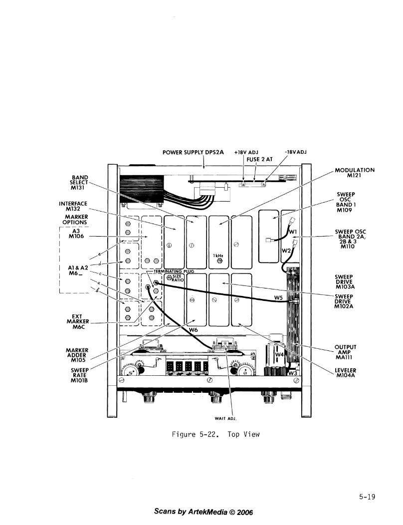
BAND SELECT M I 3 1
INTERFACE M132 MARKER
OPTIONS r 7 3 - I M I 0 6 I I
I I A l & A 2
I M 6 -
I
EXT MARKER
M M
SWEEP / OSC BAND 1 M I 0 9
SWEEP OSC BAND 2A, 2 B B 3 M l l O
SWEEP DRIVE M103A
-SWEEP DRIVE M102A
\OUTPUT AMP
MA111
SWEEP RATE
MlOlB
WAIT ADJ. I,(
Figure 5-22. Top V i e w
Scans by ArtekMedia O 2006

MODULE PIN NUMBERING
(16)
@ I 0 7 0
HOLD-DOWN 0 1 3 SCREW
0 1 4
0 1 s 2 0
ky INDEX STUD
+2O VOLT 7
MODULE PIN NUMBERING
SIZE ADJ.
'HOLD-DOWN SCREW
l M H z I O M H z S O M H z 1 0 0 M H z . . 0 0 0 . 0 . 0 . . . 0 0 . . . . . . . . e
0 . . . . . . . . 0 . 0 . . . . . . . d
o @ . 0 ~ 0 .@a 06. EX1 (1
0 a 0 O . . . 0 0
O . O . . O 0 . E
. O . . . . . . b . 0 0 . . . . .
Figure 5-23. Bot tom V i e w
M A R K E R S IZE AD J
Scans by ArtekMedia O 2006
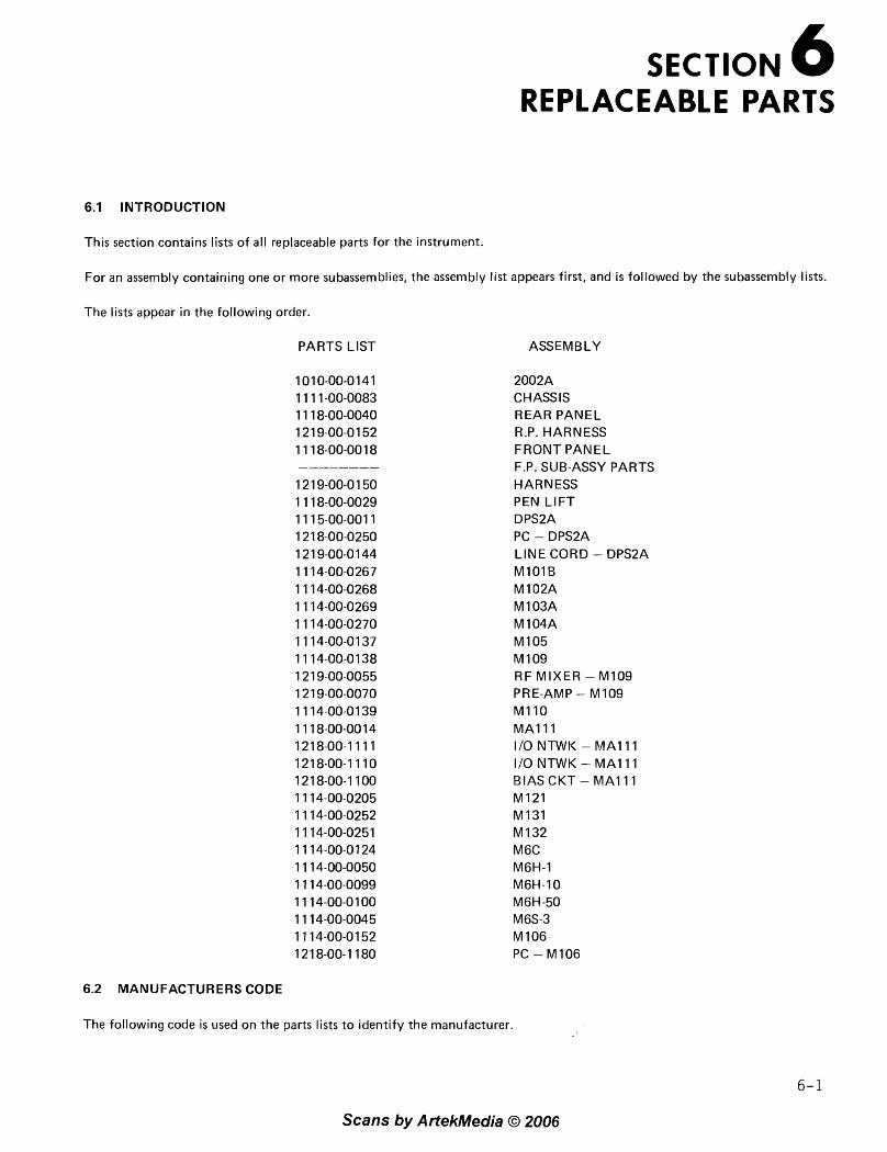
SECTION 6 REPLACEABLE PARTS
6.1 INTRODUCTION
This section contains lists of all replaceable parts for the instrument.
For an assembly containing one or more subassemblies, the assembly list appears first, and i s followed by the subassembly lists.
The lists appear in the following order.
PARTS LIST ASSEMBLY
6.2 MANUFACTURERS CODE
The following code is used on the parts lists to identify the manufacturer
2002A CHASSIS REAR PANEL R.P. HARNESS FRONT PANEL F.P. SUB-ASSY PARTS HARNESS PEN LIFT DPS2A PC - DPS2A LINE CORD - DPS2A MlOlB M 102A M 103A M 104A MI05 MI09 RF MIXER - MI09 PRE-AMP - MI09 M I 10 MA1 11 I10 NTWK - MA1 11 I10 NTWK - MA1 11 BIAS CKT - MA1 11 MI21 MI31 MI32 M 6C M6H-1 M6H-10 M6H-50 M6S-3 M 106 PC - MI06
Scans by ArfekMedia O 2006

Z
O
n
W
t- C3 a
a
n
-t a
t- z
I
1
wcn
w
a
I+ C
)
>
LO W
u
W
rC U
J W
Z
m
a
JW
>
0 J
1
0 11
U >
1
0
J
Q Q
Z
O
uL
1:
u
WW
C3
J
OW
W
Cl
OW
WA
rr
Sn
J
03 C
it
-O
JQ
I
i! W
Q
W
11 10
LL w
nw
zw
w
WI-
wc
3z
cn
u
aa
~
Z~
JJ
~~
W>
U >
t-O
OC
OJ
I- o
ca
aa
ca
cn
x u
nw
LY
>3
wI-
Orr
sn
~~
~r
>o
oc
a
a
aa
aa
>m
na
>o
~
ao
oz
oa
ow
ot-
ZO
~H
3
~3
%~
~
r<
OO
O~
IO
C
aQ
3
na
ma
oO
aW
>
Z
E>
>Z
rn
>a
~C
3Z
Oa
cb
Zu
ca
a
mZ
aa
3
11
3J
O
~O
~L
L~
I-
~Z
WU
X
~a
~~
~~
~~
~~
aa
~a
~~
~~
~~
mz
~t
-~
a~
~~
wa
a~
~~
~~
~a
zz
oa
~m
~~
a~
oa
a~
~~
~
~F
~F
uo
~F
z~
~c
~z
z~
E~
~-
Jw
u~
~~
U
CO
J~
+N
~J
W
UD
UO
DJ
~ u
as
3n
W
~Z
S~
I-
J
EF
J~
~~
L~
~Z
~~
~Q
ZZ
Z~
OQ
W~
~~
~.
WZ
O~
-L
Z~
QJ
Z~
WJ
~~
JJ
E
mJ
3u
Jn
%l
-J
ao
Ec
n
HQ
WO
~~
XW
~~
NO
OZ
~~
W~
~J
IQ
~~
I-
I~
JI
-~
QJ
W~
WW
WO
~~
~~
~~
~~
~U
UJ
~H
~~
~~
~
O~
OO
UU
UE
~~
~Z
~~
~~
I~
~~
~~
~O
~~
~O
I~
~~
~W
~L
~~
Z~
OI
I:
~~
~Z
~Z
Z~
~~
~W
~~
X~
~~

ASBRV l i l A M E . . . . . . . . . . . . . . . . . . . . . . . . . . CITY................. S T
CCM CORCOM, INC . CDC COMPONENT DEVELOPMEIJT CORP. CECO C E N T R A L C O I L CO. CGW CORNING G L A S S WORKS CHE CHERRY E L E C T R I C A L PRODUCTS CHOM CHOMERICS INC. CHRY CHRYSLER CORP. C I N C O C I M C O W I R E AND C A B L E I N C .
- 2 K I C T S K N I G H T S , I N C . C L A C L A I R E X CORP. CLAR CLAROSTAT MFG. CO C L F X COLE-FLEX CORP. CPKG C R E A T I V E P A C K A G I N G D I V . C T S C H I C A G O TELEPHONE S Y S T E N S CTS-E C T S OF E L K H A R T CTSBR C T S O F BERNE C T S S V C T S O F B R G W N S V I L L E D L D A L E TECHNQLOGY CORP. D A V HARRY D A V I E S M O L D I N G CO. D A Y T N DAYTON E L E C T R I C CO. D E L D E L E V A N D I V . D E N D E N N I S G N MFG. GO. DEW D E W I R E F A B R I C A T I N G GORP. D I L E C D I L E C T R O N DIO DIODES, I rJc . DRA D R A K E MANUFACTURING CO. E-C E L E C T R C N I C C R Y S T A L S E-M E L E C T R A / t l I C L A N D CORP. ECMC E L E C T R I - C O R D MFG. CO. It4C. E L C O E L C O I N D U S T R I E S E L F X ELECTRO-FLEX H E A T I N C . EMRON E P I T K E P I T E K E L E C T R O N I C S E T P E R I E T E C H W L O G I C A L FRODUCTS EXAR EXAR I N T E G R A T E D SYSTEMS F - K THERMWELL PRODUCTS, I N C . F-S F E D E R A L SCREW F A N FANCOURT & CO. F A S T X F A S T E X D I V . , ILL. TOOL WORKS F C D F A I R C H I L D F R K F R A K O F R T E F A I R R I T E PRODUCTS CORP. FRXC FERROXCUBE D I V I S I O N G-E GENERAL ELECTR I C G-H G R A Y H I L L , I N C . G - I GEN 'L INSTRUMENT SEMICONDUCTOR G-T GRAND TRANSFORMERS G A L G A L I L E O ELECTRO-OPT I CS GATES G A T E S ENERGY PROD. GBN G I L D E R T E N C I t J E E R I N G CO. IPJC. GNATR GENERAL A T R O N I C S CORP. GOU GGULD, I N C . G R I E S G R I E S REPRODUCER G R I P QRIPMASTER CO. GUDL L'UDEBROD BROS. S I L K CO. H-P HEMLETT-PACKARD
C H I C A G O CARSON B R A Z I L CORN1 WG WAVKEGAN WOBUR N D E T R O I T A L L E N D A L E SANDWICH MT. VERPtON GOVER B A B Y L C N I N D I A N A P O L I S C H I C A G O E L H H A R T BERNE GROWNSVILLE H A R T S D A L E C H I C A G O ZHICAGr3 EAST AURORA F R AM I NGH AM L C l J E L L MOtJROVI A CHATSWORTH HARWOOU H E 1 GHTS KANSAS C I T Y M I N E R A L WELLS WESTF I E L D HClCKFt3RD 13LOOMFIELD
XANATA, (3NT.I CAN. E R I E SUNlJYVALE FRAM I NGHAM C H I C A G O GREENSBORO DES P L A I N E S M O U N T A I N V I E W FRANKFORT, GER. W A L L K I L L S A L i G E R T I E S I N D I A N A P O L I S L A GRANGE H I C H S V I L L E GRAND H A V E N C ARMEL DENVER P H O E N I X P H I L A D E L P H I A ST. P A U L N E N R O C H E L L E MARLBORO C H I C A G O I t 4 D I A N A P C L I S
Scans by ArtekMedia O 2006
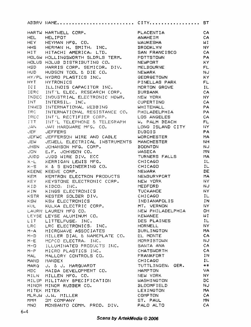
ABDRV t \ i ' A F I E . . . . . . . . . . . . . . . . . . . . . . . . . . CITY.. . . . . . . . . . . . . . . . S T
HARTtk H E L H E Y H H S H I T I-iULC;W WQLCJU I i S D HUE) W Y / P L I-iY T I C I IEEr:: I fL'zEi2 I XT I t.jNE3 1 T . i !: I T-? E C T 1' i I I
[<
..! E F' JEFWC ,-i E W Jt-fSV JCN J C J D D *-i
K - - 5 KEENE KErI KEY ti 1 D K I N HSTR K.SN p, (l! !-. L.A!IRP.! L.EYSE L I T L R C 5 -k 1.; -- rj f.i -E !'q .- 0 !I- P :I A L MANU f+kRQ PI 11 e M I L N T-IILSP M i NG2 i? I TECi MLR J W M M 11 fil\iC1
6-4
H A R T M E L L CERP. H E L I P O T HEYt?AN ItIFG. CO. HERt?Af'J H. S M I T H , I N C . H I T A C H I A M E R I C A , L-TU. t4OLLINGSWORTI-l S L C R L S TERM. HOLUB DISTRIDUTINC cn. H A R R I S CQRP. S E M I C D R . D I V . HUDSON T O O L Z: DIE CC3. HYDRO P L A S T I C S I N C . liY TR@N I C S I L-1. I t i 0 I S CAPAC I TOR I NC. I LdT-'L.. E L E C . R E S E A R C H C,ORP. I N D l i S T R I A L E!..ECTRC!rJ I C tiDL4t?. IP. lTERSIL, I N C . I NTERNAT I QITAI- llEI31! I l 4 r 2 ItJTER!.JkTIC!P!AL. RESISTAr4CE <I.'(]. 1 I ? T 'L. A E I Z T I F I E F ! CORP. 1 l.JT' $1. TEL.EiJf.iOP;E i?'Ei.i:GR&+Pt+ ..IC11! HARB1JARE !?I'G. CCI. X F F E H S JEFFERSO?.! W I R E AND C A B L E JE:!ELL E L E C T R I C A L I I\ISTR'JMENTS JGHAt\ !SON I'iFG. CGRP. E. F. JEHXSPN CO. C!,IDD LJIRE aIv. ECC H E R R I G A N L E W I S MFG. K 81 S E N S I N E E R I N G CO. K E E l i E CQRP. KEMTRON E L E C T R O N PRODUCTS K E Y S I O r 4 E E L E C T R O N 1 C CCjHP. M I D G O > 1/12. %. i.l tJGS EL.EGPRC::.II C'S K E S T E R SOLDER D I V . 6.SW E L E C T R C N I C S K V L X A E L E C T R I C CQRP. L-AC1UEN T'IFC CE. L E Y S E ALVfI INVPi Cf l . L 1 T T E L F U S E * I N C . L R C E L E C T R O N I C S . . I tdC. III CRGWkLJE ASSCIC I A T E S r v i I L i . E R P1D.L. 3 N A M E P L A T E CU. T?EPCCl E L E C T E R , I ldC. l i L . i J l l f !%J4TEU 42CILjVCTS I t:C. M I C R U P L . A S T I C S I IJC. M 4 L L G R Y CENTROLS GO. t71AP21)EX J n t J. tIARQUAI?I)T MA I DA E E V E L O P M E R T CQ. P I I L L E N t lFG. CO. f ? I L I T A R Y SPEC;IF' ICATIOt. I M I N 6 R RVZBER GO. f l I IEK .J. i d . t1 IL.L.ER 3x COMPANY MC:..ISAt.!TCI COMtI. PROD. f) I V.
P L A C E t \ 1 T I A A N A H E I M K A U K E S H A 3 R O O K L Y N S A N F R A N C I S C O POTTSTOWN NELJPQRT tlELI3OUR N E tJEWARK GEORGETOWN P I N E L L A S P A R K MORTON GROVE BURBANK r!EW YORK C U P E R T I N U WH I T E t i A L L P H I L . A D E L P t i 1 A L-CIS A N G E L E S W. P A L M D E A C H L-ONG I S L A N D C I T Y D U 3 O I S WORCHESTER MANCHESTER BOON7'01\1 l t lA6EC A TURNERS F A L L S C H I C A G O C H I C A G O NEldARK tdEW3URYPGRT NEW Y a R K 14OT)FURD T U C K k H O E C H I C A G O I ND I ANAPOL- I S M r . VERNON rdEW P t i I L A D E L P H I A KEWANEE EIES P L A I IJES HORNELL. 3 U R L I N G T U N EL. tlClt4TE CIORR I STCICJN SAtdTA ANA CHATSWORTH F R AtJKFORT C H I C A G O T U T T L I N G E N , GER. HAMPTON tJEIJ YQRK WASHINGTON DLOOMF l E L D L U X I NGTOF4 C Ql lP TON S T . P A U L P A L O A L T O
Scans by ArtekMedia O 2006
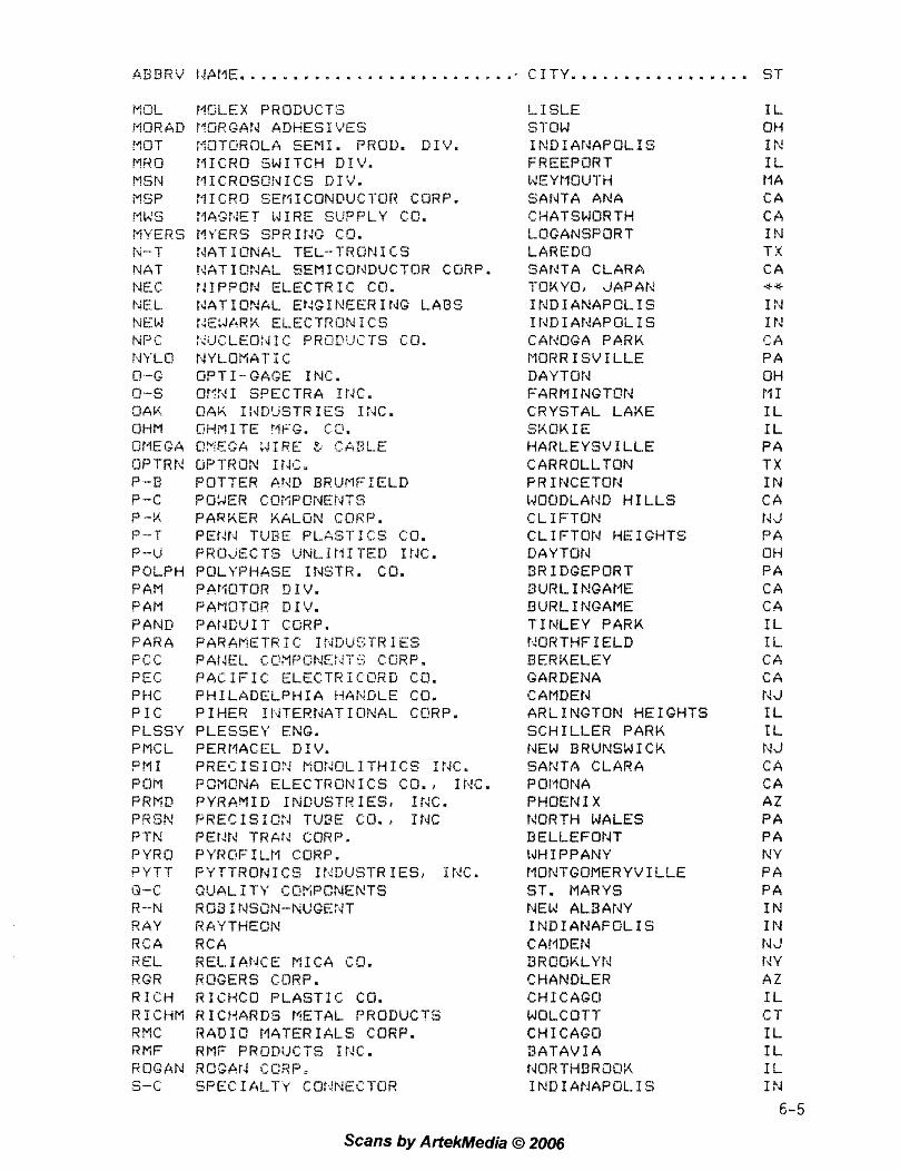
A3!3EV 12BtIE.. . . . . . . . . . . . . . . . . . . . . . . . .- C I T Y . . . . . . . . . . . . . . . . . ST
iy!lL MGRAD 307 WHi3 MSN M C 2 P , ! .d Mi ! I*L
fl\i'EFi.S I<- T NAT NErfl PEL. NEW NPC NYLCI 3-Q 0.-S 3 A K UHM CPIEGA QPTRN P -B P-c P -% P-T P-U POLFll PAM P A M PAP.lfr P A R A p i; C PEC P 1-4 C P I C FLSSY P M C L P M I PC3M F3RKLt PRSN PTN PYRQ P Y T T Q-C R--N R A Y RCA r?EL RGR R I C H F i I C t i M 2MC R M F RClGAN .-. *-c i-I
NGLEX PROCUCTS tAsRG&!.f AT)HES I1.+!ES XOTr iRQLA SEMI. PHCIU. D I V . P i I C A D S W I T C H D I V . MICR@SC.?NICS D I V . M I C R O SEKICONQUCTUR CQRP. :.IAGf,jET LJIRE SC!?T;LY C Q . tSYERS SPRILdC (10. !4AT I ORAL T E L - - T R I M 1 CS I4AT I C!NAL SEM JCr31?DUCTOR CClRP. T! f PPCfil E L E C T R I C C0. tGAT I DNAL EfdS I NEER I NG L A B S NELJARK E L E C T R O N I C S :Ci_lcLE::Q:.,/Ic PRsLi\-!i_'-rS CCI. F4YLCIMATiC G P T I - - GAGE INC. f)Yf41 SPECTRA I f J C . OAK I ldL)tiSTR I E S I TdC. I G * C f i . C!YF:Z:k :JIF:E z; :ek3L.E CiPTRCIN I I?::. P O T T E R AND BRUMFrLELD PGXER CZNPCNEFJTS PARKER X A L G N CCIRP. PEt2I.I TUEE P L - A S T I C S CU. PFtOjEC TS UNL.1 III TED I rJC. P O L Y P H A S E I N S T R . CO. PAr5OTOR D I V. PAptOTOR D I V. Pnt4CY I T CCRP. PARklvjETR I C Ir\iDi-iSTH I ES P,t+[!EL. C.QxPc':NE:.i?'S CfiHP. P A C I F I C : E L E C T R I C P R G CO. P H I L A D E L P H I A HAPXiLE CCI. P I HER I l'dTERt4AT I O N A L CC!RP. PLESSEY ENG. P E R M A C E L DIV. PREtZ ISIU?< KOGUL. I T H I C S I N < . FOtlilNk E L E C T R O N I C S CO., If.!Z. P Y I l c ? V I B INGUSTDIES, INC. P R E C I S I C P J TUBE CCI., I N C PEt!t\! TFiAt-d CORP. PYREFIL.I.1 CORP. T-Y T T R O N I CS I R D U S T R I E S , I?,'C. Q U A L I T Y CEKPCNENIS RE3 INSZN-KUGErJT F? A'r'THErJN RCG R E t . i A N i " E M I C A 2 0 . EQGERS CORP. R I C H C O P L A S T I C CG. R I C HAR DS F E T A L PRODUCl -S R A D I G M 4 T E R I A L S CORP. RMF P R O D U C i S I!..!C. RCx2AN ZGZP, SPEC I A L T Y COPINECTCIR
L ISLE ST@N I N D I A t 4 A P : Q L I S F R E E P D R T WEYtIQV1-H S A N T k ANA CHATEjLbORTH LOCANSPORT L A R E D B SANTA C L A R A TOKYC], JAPAN I N D I A N A P O L I S I tGD I Ar4APOL I S CAt.:'OGA PARK M O R R I S V I L i E D A Y TON F A R M I N G T O N C R Y S T A L LAKE SKUK I € H A R L E Y S V 1 L L . E C A R R O L L T O N P R I N C E T O N WOODLAt4C H I L L S C L I F T O N C L I F T O N H E I G H T S DAYTGtJ B R I D G E P O R T 3URL I I\!GAME B U R L I N G A M E T I N L E Y PARK N O R T H F I E L D B E R K E L E Y (3ARDEtdA CAt lDErJ A R L I N G T O N H E I G H T S SCHILLER P A R K NEW I 3 H U N S M I C K SANTA C L A R A POI'IONA P H O E N I X NORTH WALES B E L L E F O N T lJH I P P A N Y tlOt4TGOMERYV ILLE ST. M k R Y S NEW A L B A N Y I N D I A N A F G L I S CAMDEN 3ROC3KLYN CHANDLER C H I C A G O WOLCOTT C H I C A G O 3 A T A V I A r4ORTtiBRi30X I N D I A N A P E L - I S
Scans by ArtekMedia O 2006

A n B R V IIffttlE.. . . . . . . . . . . . . . . . . . . . . . . . . C I T Y . . . . . . . . . . . . . . . . . ST
C-G ,A STkl4EARD tl:H IG513Y A?IRUP.A -. .. .r : SW I Tc"HCHAF1-7 I td:Zrn CH I CAGO - .-. ,.. -.- . -I ~ ? E R V I CE ~ i ~ p p i - Y I I A N A P G i I rj C 2 - T I-: S,+F?XES Z I A r ? 3!-.CinM I t4i:TCltd S C ~ ~ E SCATJBE DIVISION EL TIUTJTE \? i- :- ,", ..: s-. SIACk2,.'\Pcj:--E: Z+$R391\! CC]. 27-. MAR'fS , - r n ., .-, sJLIc_^f)!!,I:f I N C . SAt4TA C L A R A ,-, ..- :,1:&.+5i' Sf<$.S1-Rc?;q i?FG. ~~~. i; ' iEf\iDkLE SEZR 5 ~ ~ r . i ~ 112f . . I2ESTWUC)D SEL F X A L U C T R O GORP. I l k t l kRONECH SEE SEMTECH NEWBLJRY PARK SEMTX SEMTEX DAYTON 172M 5 I G t ? A I ~.LSTR(- l t~Et~JTS 3 H A I N T R E E :3ldhM SI-IAMIIUCX PLAST ICS % RUBBER Ci l . I N I ) I A N A P Q L f S SIEM SIEI' iErdS I S E L I N SIG S I G r 4 E T I C S CORPORATION SUr4PtYVALE 3 i . T 5f i i I IRC!N./MICFic3k'kVE D I V . FORT SALERNO StYiiC SArITEC IIJC. NEW A L n AtJY SOLJTH SOCjTHCr3 F4STETJEHS L E S T E R SPE SFECTRGL DAYTON SPEC SPECTRUM CONTROL. IEdC. I r A I R V I E W SPR SPRAGVE E L E C T R I C CU. I KD I Ab!kPCL I S S P S T SPECTRA-STH I P 'GARDEN GROVE SSS S G L I D S T A T E SCIE t4T I F I C MOrdTGOMERYV I L L E sTDPS STANDARD PRESSED S T E E L JEI4H I I4TOWN ST'R STETTNER TRUSH CU. C A Z E N O V I A S T S A S T E E L S A L E S I tdU I A N A P C L I S S Y L GTE S Y L V A N I A WALTHAM SYS SYSCQN I N T E R N A T I C N A L , I N C . SOUTH BEND T.- I T E X A S I NST'RUMENTS D A L L A S TCPL TACQNIC P L . 4 S T I C PETERSBURG TEK T E K T R O N I X I N D I A N A P O L I S TEKA TEKA PRODUCTS I N C . CULLEGE P O I N T T E L E T E L E T Y P E CORP. E L K GROVE V I L L A G E TI-4R THERMALLOY CO. D A L L A S T I M E S T I M E S W I R E AND C A D L E C I t4C I NIJA I T I N TINI4ER!'!Atd PRDDUCTS, I ttC. CLEVELAIJD TKN T E C H N I C A L IdIRE CRAWFORIj TLNC T E L O N I C A L T A f R L A O U N A BEACH TORCO TOR CORP. LJATJ NUYS TR-LJT TR IAD-UTRAD D I V . HUNTINGTCIN T'RU !JALDES TRUARC LOtdG I S L A N D C I T Y T-RN TRlJ CAPACITOR D I V . O G A L L A L A T V L T E L - V I S I O N L A B S LJAUCONDA U-C VNIVERSAI, COt lPQNEr lTS L a S ANGELES UNCAR U N I (3rd C A R B I D E COMPOrJENTS G R E E N V I L L E U N I C UrJICCRP ORANGE U N I T U N I T R O D E CORP. WATERTOWN USECO LiSECO D I V . VAt4 NUYS UTK U N I T R A C X D I V . UPPER DARBY 'JAC C'ACTEC INC. MARYLAND HE I GHTS VACO VACO PRODUCTS CO. NORTHBROOK VAR VARADYT-!E CAPACITOR D I V . SANTA MONICA V A R I L V A R I - L CO. DENVER VELCR VELCRO USA I N C NEW YORK V L I E R V L I E R E N G I N E E R I N G GORP. DURBANK
6-6
Scans by ArtekMedia O 2006
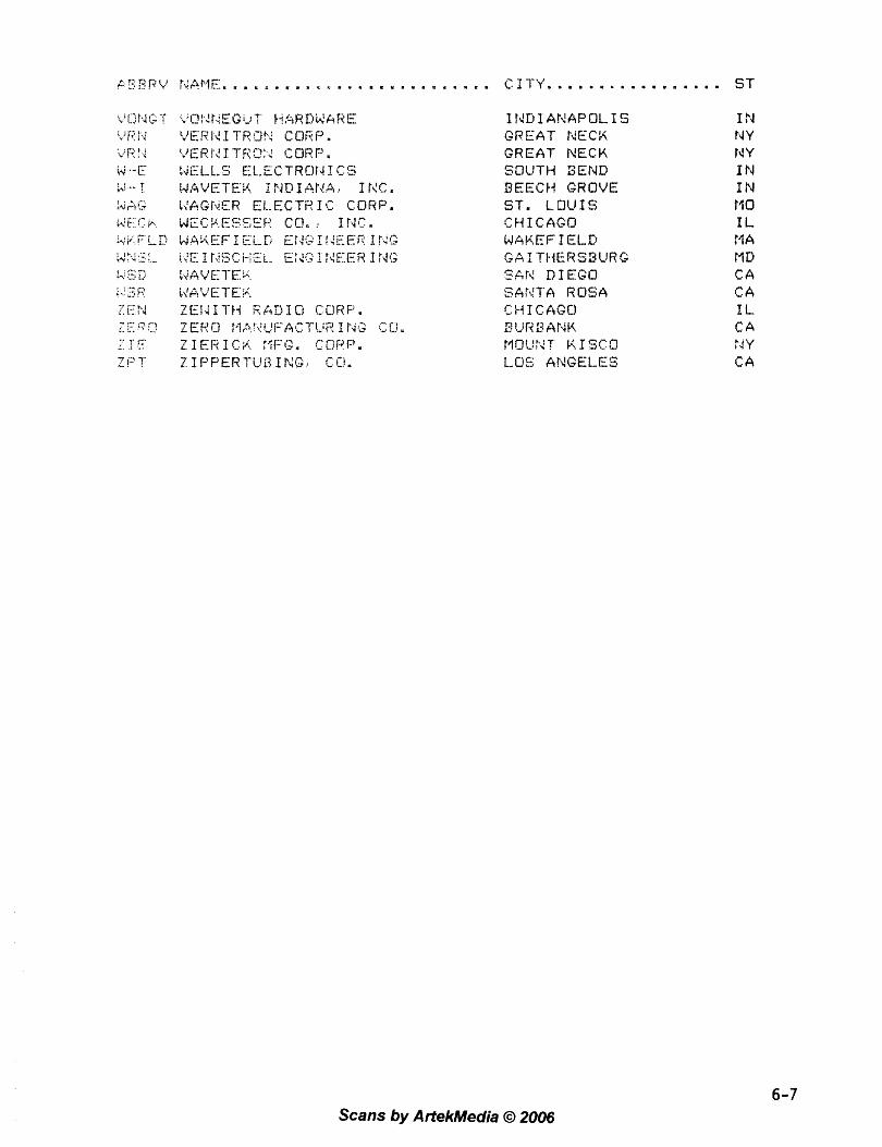
P?:BFV T::tPlE. . . . . . . . . . . . . . . . . . . . . . . . . . C IVY. . . . . . . . . . . . . . . . . ST I t4D I Ar4APQL IS GREAT N E C K GREAT NECK SOUT1-i SEND J3EECW GROVE ST. LOUIS CHICAGO WAKEFIELD GAITHERSBURG SAl4 DIEGO SA:,!T'A ROSA CI-i I CFsGU B 'J TI :3 A r.4 K r/tnC!t't r' C.; I SC:O I-UE ANGEL-EB
Scans by ArfekMedia O 2006


J 6 I CONN, BNC, d E O O 0 - 0 2 3 / K C 7 9 - I 6 7 1 K I N 1 2 1 1 0 - 0 1 - 1 0 0 9
REFERENCE DESIGNATORS
C 0 1
I C 1
R 2 4
R 2 5
REFERENCE DESIGNATORS
5 5 S 6 I SWITCH, TOG, E L K A N O ~ 7 1 0 1 P N ( C-K 1 5 1 0 6 - 0 0 - 0 0 0 9
MFGR
T R U
MOT
A-B
ASE
PART D E S C R I P T I O N
CAP, TANT,. 47MF' 5 0 V C E 1 1 3 - 4 4 7
I C , ICOOO-026
POT, i K R P 1 2 4 - 2 1 0
RES, C, 1/4W, 5%. 2 K RC 103-220
PART D E S C R I P T I O N
ASSEMBLY NO.
1 1 1 8 - 0 0 - 0 0 4 0
REV
UAVETEK NO.
1 5 1 0 - 2 1 - 9 4 7 0
7000-78-1800
4 6 1 0 - 1 0 - 7 1 0 2
4 7 0 0 - 1 5 - 2 0 0 1
ORIG-MFGR-PART-NO
935
MC7818CD
WA2G032S-102MA
C F i /4 -2K
WAVETEK PARTS LIST
PAGE 1
GTY
1
1
1
1
ASSEMBLY NO. 1111-00-0083
PAGE: 1
WAVETEK PARTS LIST
ORIG-YFGR-PART-YO
TITLE
REAR PANEL 2 0 0 2 A
REV
TITLE C H A S S I S 2 0 0 2 4
MFGR
Scans by ArtekMedia O 2006
WAVETEK NO.
REFERENCE DESIGNATORS
P3
NONE
PART D E S C a I P T I O N
H S G , M I N I - L A T C H , 5 - P I N
TERM,MALE,MCOOO-116
ORIG-MFGR-PART-NO
6 5 0 3 9 - 0 3 2
4 8 1 1 6
REV ASSEMBLY NO. 1 2 1 9 - 0 0 - 0 1 5 2
PAGE: 1
WAVETEK PARTS LIST
MFGR
BER
BER
TITLE HARNESS 2 0 0 2 A - D
WAVETEK NO.
2 1 1 3 - 1 0 - 0 0 0 1
2 1 1 3 - 2 2 - 0 0 0 1
QTY
1
4
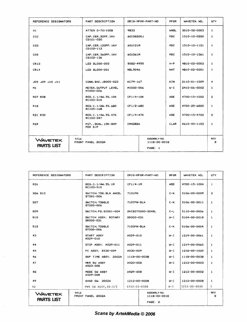
I REFERENCE DESIGNATORS 1 PART DESCRIPTION 1 OR IG-MFGR-PART-NO I MFGR WAVETEK NO.
3 0 1 0 - 5 2 - 0 0 0 3
1 5 1 0 - 1 0 - 0 2 0 0
QTY
1
1
ATTEN O-70 / lODB WNSL
MDC CAP. CER. 2OPF8 1XV C D l 0 1 - 0 2 0
MDC CAP, CERt 12OPFj 1KV CD102-112
MDC CAP, CERt 3 6 0 P F t 1KV C D l 0 2 - 1 3 6
H-P
NAT
K I N
W-I
LED D L 0 0 0 - 0 0 3
LED D L 0 0 0 - 0 0 1
J 0 5 J09 J l O J l l
M 1 METER, OUTPUT LEVEL M I 000-006
R 0 7 ROB ASE
ASE
C F l /4 -47K I AsE POT., DUAL, 1OK-OHM PER B / P
1 CM42826 1 CLAR
REFERENCE DESIGNATORS I PART DESCRIPTION I ORIG-MFGR-PART-NO I MFGR
I
WAVETEK NO.
4 7 0 0 - 1 5-1 0 0 4
wAvE~EK PARTS LIST
QTY
TITLE FRONT PANEL 2 0 0 2 A
ASE
SWITCH, TOG, BLK ANOD. S T 0 0 1 - 0 0 6
7 1 0 1 P N I C-K
SWITCH, TOGGLE S T 0 0 2 - 0 0 6
SWITCH, PB, S Z 0 0 1 - 0 0 4 C-L
W - I SWITCH ASSY, ROTARY SR000-031
SWITCH, TOGGLE S T 0 0 0 - 0 0 6
START ASSY A 5 2 9 - 0 1 0
W-I
I STOP ASSY. A 5 2 9 - 0 1 1
I PC ASSY. 3 5 3 0 - 0 0 9 W - I
W-I SUP T I M E ASSY, 20026
MKR St4 ASSY A 5 2 3 - 0 0 8
W-I MODE SW ASSY A 5 2 9 - 0 0 8
BAND SW, 2 0 0 2 A
4 2
WAVETEK PARTS LIST
PWR SW A S S Y , 1 6 - 1 / 2
FRONT PANEL 2 0 0 2 A REV
B
~ -
Scans by ArtekMedia O 2006
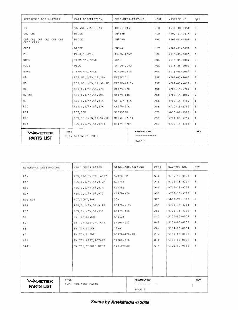
ORIG-MFGR-PART-NO MFGR
I REFERENCE DES!GNATORS I WAVETEK NO. PART D E S C R I P T I O N
l O T C C - Q l 5 1 SPR
CR2 CR3 1 D I O D E FCD
P-C
H I T D I O D E
P L U G , 3 6 - P I N
CR4 CR5 CR6 CR7 CR8 C 9 9 C R l O C R l l
NONE
P 2 0 1
D I O D E
0 2 - 0 9 - 2 1 1 8 1 MOL NONE ( TERMINAL ,MALE
C F - ! / 4 - 4 ? K / ASE
AS E
CTS
M F 5 5 K - 4 7 . 5 K ( ASE
C F 1 / 4 - 4 7 0 K
REV
AS E
WAVETEK PARTS LIST
I PAGE 1
ASSEMBLY NO.
------------ TITLE
F .P . 5119-ASSY PARTS
REFERENCE DESIGNATORS P A R T D E S C R I P T I O N ORIG-MFGR-PART-NO MFGR WAVETEK N(1.
I R l 4 RES,P/O S W I T C H ASSY W- I
A - 3
A - 3
AS E
SPE
AS E
ASE
S-ru
W- I
OAK
C-W
RES,C, 1 /4W,58 ,4 .7M
RES,C, 1/4W, 5 % , 4 7 H
RES,C, 1 /4W, 5%, 4 7 0
POT, COIdT, 1 0 K
RES,C, 1 /4W, 5%, 4 . 7 K
RES,C, 1 /4W, 5%, 3 3 K
SWITCH, LEVER
1 s 2 ' S W I T C H ASSY, ROTARY I
I s 3 I SWITCH, LEVER
S I i I T C H , S L I D E
S W I T C H ASSY, ROTARY
SWITCH,TOGGLE DPDT
REV WAVEPEK TITLE
F . P . SUE-ASSY PARTS
I ASSEMBLY NO.
I ------------
Scans by ArtekMedia O 2006
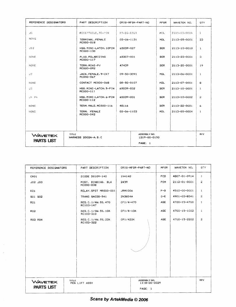
-- 7
REFERENCE u E s I W A T a R s / P l i i i T ~ E s c R l P i l o r d 1 a . I + M F G r 3 - P * R r - N l j 7 n F E R wAvETEK NO. I-& 1
J 1
NONE
J 1 2
NONE
NONE
J 2
NONE
2 ;
J4 P 4
NOqE
NONE
RCCE?T4CLE,Z5-PIN
TERMINAL, FEMALE M C O 0 0 - 0 1 6
HSG, M I N I - L A T C H , i O P i N MC000- 130
PLUG, POLAR1 Z I N G MCOOO-117
TERM, M I N I - P V M C 0 0 0 - 0 9 2
JACK, FEMALE, 9 -CKT PCOOO-067
CONTACT M C 0 0 0 - 0 6 8
HSG, M I N I - L A T C H , 5 - P i M M C 0 0 0 - 1 1 l
HSG, M I N I - L A T C H , & - P I N M C 0 0 0 - 1 1 2
TERM, MALE, M C 0 0 0 - 1 1 6
TERN, F E M A L E M C 0 0 0 - 0 4 2
NCL
MOL
BER
BER
BET!
MOL
MOL
BER
BER
BER
MOL
REFERENCE DESIGNATORS
w 2 k v ~ T ~ ~ m LIST
P A R T D E S C R I P T I O N
TITLE ASSEMBLY NO.
HARNESS 2002,-A, B, C I 1 2 1 9 - 0 0 - 0 1 5 0 . 1 P A C E . l
--
D I O D E D G 1 0 9 - 1 4 0
PUST, B I N D I N G , DLK MCO00-038
K O 1 i RELAY, SPST M R 0 0 0 - 0 0 1
RES. C, i / J W , 5%, 22K RC 1 0 3 - 3 2 2
1 -- -
TITLE WAMTEK I P E N L I F T A s s Y
MFGR
F C D
PUM
P -B
C-E
ASE
ASE
ASE
ASSEMBLY NO. :1!8-30-0029
PAGE: 1
WAVETEK Nij. GTY
j
2
i
2
2
REV
Scans by ArtekMedia O 2006

REFERENCE DESIGNATORS PART DESCRIPTION
FUSE. SLO BLO. 1 AMP. 250V
POS. VOLTAGE REG.
CONN, 6-P IN, KONEKTON MC000-076
RECEPTACLE
CONTACT. MC000-131
PROT PWR DARLINGTON
SWITCH. SLIDE. DPDT
XFMR, PWR
PC ASSEMBLY. DPS2A
L I N E CORD ASSEMBLY
ORIG-MFGR-PART-NO
MDL-1
19-09-1042
08-50-0106
LM395T
EPSI-SLI
8720
1218-00-0250
1219-00-0144
MFGR
BUS
NAT
MOL
MOL
MOL
NAT
S- I
A-M
W - I
W - I
ASSEMBLY NO.
1115-00-0011 wAVE~EK PARTS LIST
WAVETEK NO.
2410-05-0005
7000-03-1700
2113-06-0002
2113-26-0002
2113-07-0002
4902-00-3950
5105-00-001 1
5610-00-0027
1218-00-0250
1219-00-0144
TITLE
POWER SUPPLY, DPS2A
QTY
REV
C
CROl
CR02 CR04
CR03 CR05 CRO8
CRO6 CR07
FO 1
REFERENCE DESIGNATORS
CAP. CER. .005MF. 100V
PART DESCRIPTION 1 CAP. CER. .005MF, 100V
CAP. ELECT, IMF. 25V CE120-001
CAP, ELECT. 100MF. 25V CE105-110
CAP. 10000MF. l 6 V CE122-310
CAP. TANT. 1OMF. 25V CE120-010
DIODE BRIDGE
DIODE DG109-140
DIODE DR000-001
DIODE DR000-009
FUSE. S. B. 8 2AMP MF000-002
VOLTAGE REFERENCE
DUAL OP AMP
CONN., RECEPT., 3-PIN
- -
ORIG-MFGR-PART-NO MFGR I WAVETEK NO.
SPR 1510-20-4101
SPR
SPR
SPR
SPR I 1510-21-4103
1510-10-2502
1510-10-2502
1510-21-7010
SPR 1 1510-21-7100
MOT
FCD
P-C
G-E
L I T
4806-02-0003
4807-01-0914
4806-01-4004
4806-01-5624
2410-05-0001
P H I
T - I
AMP
I ASSEMBLY NO.
1218-00-0250
7000-00-0200
7000-00-8200
2112-25-0001
WAVETEK
Scans by ArtekMedia O 2006
TITLE PC ASSEMBLY. DPS2A
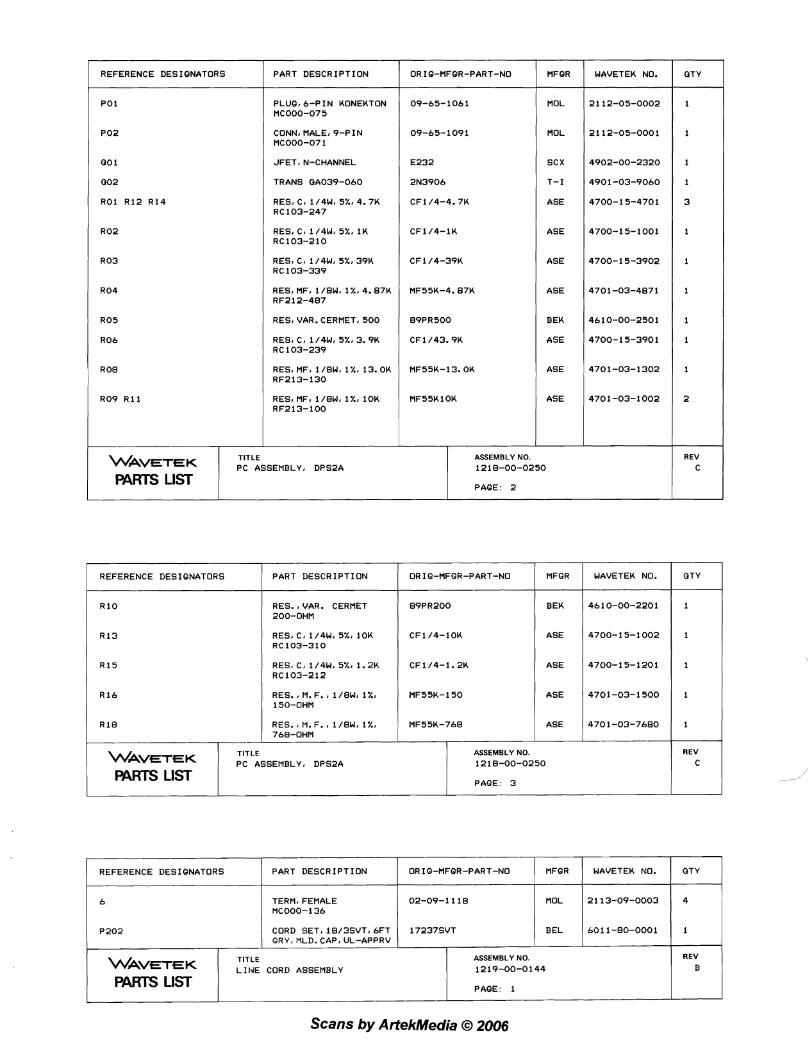
WAVETEK NO. L= REFERENCE DESIGNATORS
PLUG, 6 - P I N KONEKTON MC000-075
CONN, MALE, ? -P IN M C 0 0 0 - 0 7 1
PART D E S C R I P T I O N
MOL
SC X
T- I
I JFET, N-CHANNEL
ORIG-MFGR-PART-NO
I TRANS QAO39-060
MFGR
ASE
ASE
ASE
ASE
I R05 1 RESI VAR. CERMET, 5 0 0 I 89PR500 I BEK
ASE
I ASSEMBLY NO. 12 1 8 - 0 0 - 0 2 5 0 wAVE~~K
I PAGE: 2
TITLE P C A S S E M B L Y 8 D P S 2 A
REFERENCE DESIGNATORS 1 PART DESCRIPTION I MIG-MFBR-PART-NO I MFGR WAVETEK NO. QTY
RES., VAR. CERMET 200-OHM
BEK
ASE
ASE
ASE RES.. M. F. , 1/8W, 1 % ~ 1 SO-OHM
ASSEMBLY NO. 1 2 1 8 - 0 0 - 0 2 5 0
REV
C
( REFERENCE DESIGNATORS I PART DESCRIPTION I ORIG-MFGR-PART-NO ( MFGR I WAVETEK NO. I QTY I
w - ~ ~ K rn LIST
TERM, FEMALE MC000-136
TITLE P C A S S E M B L Y J D P S ~ A
MOL 1 21 1 3 - 0 9 - 0 0 0 3 1 4 1
CORD SET, 1 8 / 3 S V T , AFT GAY, MLD. CAP, UL-APPRV
TITLE wAvE~EK L I N E CORD ASSEMBLY
ASSEMBLY NO. 1 2 1 9 - 0 0 - 0 1 4 4
I PAGE: 1
Scans by ArtekMedia O 2006

I REFERENCE DESIGNATORS I P A R T DESCRIPTIC IN I ORIG-MFGR-PART-NO / MFGR I WAVETEK NO. ( QTY 1 C O l C 0 2 C 0 3 C 0 4 C 0 5 C 0 6 C 0 7 C 0 8 C 1 8 C 1 9 C 2 0 C 2 1 C 2 2 C 2 3
C l O C 2 6
C l l c i a
C R O l C R 0 3
C R 0 2 C R 0 4 C R 0 5 CRO6 C R 0 7 C R 0 8 C R 0 9 C R l O C R l l C R 1 2 C R 1 3 C R 1 4 C R 1 5 C R 1 7 C R l 8 C R 1 9
CAP, F. T., 6 . 8 P F C F l O 2 - R 6 8
CAP. MYLAR, . 15MF. 1 0 0 V C P 1 0 3 - 4 1 5
CAP, CER* . OOIMFD, 1 K V C D l 0 2 - 2 1 0
CAP, CER. 4 7 0 P F . 1 K V C D l 0 2 - 1 4 7
CAP, CER, . O ~ M F I 1 0 0 V C D l 0 3 - 3 1 0
CAP. CER, I O P F . 1 K V C D l O l - 0 1 0
CAP, F. T. 8 4 7 0 P F C F l O l - 1 4 7
D I O D E D R 0 0 0 - 0 0 1
D I O D E D G 1 0 9 - 1 4 0
C-D
SPR
SPR
MDC
SPR
MDC
SP R
A-B
P-C
FCD
A-Q 1 5 1 0 - 3 0 - 1 6 8 9
ASSEMBLY NO. 1 1 1 4 - 0 0 - 0 2 6 7 wAVE~~K
PARTS LlST
REV
B TITLE SWEEP RATE, M l O l B
REFERENCE DESIGNATORS
CR2O C R 2 1
I C l
I C 2
I C 3 I C 4 I C 5
I C 6
Q l
Q 2
03
0 4
R O l
RO2 R6O
R 0 3
R 0 4 R 1 4 R 4 0
R 0 5
P A R T D E S C R I P T I O N
OP AMPL TO-5 I L O O 3 - 0 0 4
I C . ICOOO-002
I C , ICOOO-005
D U A L OP AMP
TRANS Q B 0 0 0 - 0 0 9
TRANS G A 0 3 8 - 5 4 1
TRANS Q A 0 5 4 - 5 8 0
TRANS Q A 0 5 4 - 6 1 0
RES, C, 1 / 4 W, 5%, 4 3 K RC 1 0 3 - 3 4 3
POT, 2 0 K . R P l 2 9 - 3 2 0
RES, MF, 1 /8W, I%, 8 8 . 7 K R F 2 1 3 - 8 8 7
RES, C, 1/4W. 5%, 1 5 0 K R C l 0 3 - 4 1 5
RES. C, 1 /4W* 5 % ~ 2 7 K R C l 0 3 - 3 2 7
ORIG-MFGR-PART-NO
C F l / 4 - 2 7 K
WFGR
N A T
S I G
RAY
T- I
MOT
G-E
MOT
MOT
ASE
C T S
ASE
ASE
ASE
I ASSEMBLY NO. 1 1 1 4 - 0 0 - 0 2 6 7 wAVE~~K
PARTS LlST I PAGE: 2
TITLE SWEEP RATE, M101,
WAVETEK NO. QTY
Scans by ArtekMedia O 2006

MFGR QTY
1
2
3
4
2
2
6
1
3
1
2
1
REFERENCE DESIGNATORS I PART DESCRIPTION ORIG-MFGR-PART-NO WAVETEK NO.
4700-1 5-1001
4700-15-8202
4789-00-0004
4700-15-1203
4700-15-1202
4700-15-1204
4700-15-4702
4700-1 5-1 504
4701-03-4872
4610-00-1202
4700-15-2202
4701-03-4422
RES, C, 1/4W, 5%. 1K RCl03-210
RES, C. 1/4W, 5% 82K RC 103-382
RES. SET, 2-1OK, 1 /8W QTY: 2 : 4701-03-1002
RES. C, 1/4W. 5%, 120K RCl03-412
RES. C. 1/4W. 5%. 12K RCl03-312
RES, C, 1 /4W, 5%, 1.2M RC103-512
RES. C. 1/4W. 5%. 47U RC 103-347
RES, C, 1 /4W. 5%. 1. 5M RC103-515
RES, MF, 1 /8W, l%, 48.7K RF213-487
POT, 2K. RP129-220
RES. C. 1/4W4 5%. 22K RC 103-322
RES, MF. 1/8W, 1 % ~ 44.2K RF213-442
CF1/4-1K
C F l /4-82K
RX000-003
CF1/4-12OK
CFl /4-12K
CFl/4-1.2M
CFl /4-47K
CF1/4-1.5M
MF55K-48.7K
360S202B
C F l /422K
MF55K-44.2K
ASE
ASE
W- I
ASE
ASE
ASE
ASE
ASE
ASE
CTS
ASE
ASE
wAvE~EK PARTS LIST
REFERENCE DESIGNATORS I WAVETEK NO. :Ty
4701-03-5622
4700-15-4704
TITLE SWEEP RATE, tI101B
ORIG-MFGR-PART-NO PART DESCRIPTION
ASE
MFGR
I CFl /4-56K I ASE
ASSEMBLY NO. 1114-00-0267
PAGE: 3
ASE
REV
I3
ASE
ASE
C F l /4-2.7K ASE
ASE
I ASE
ASE
ASSEMBLY NO. 1114-00-0267
I PAGE: 4
wAvE~EK , PARTS LIST
Scans by ArtekMedia O 2006
TITLE
SWEEP RATE, M l O l B
REFERENCE D E S I G N A T O R S P A R T D E S C R I P T I O N
R E S t C t 1 /4W, 5 % ~ 3 3 0 K RC 103-433
RES. C, 1 /4W. 5%, 1 8 0 K R C 1 0 3 - 4 1 8
RES, C J 1 /4W, 5 % 1 3 0 K RC 103-330
RES, C t 1 / 4 W t l o % , 1OM R C l 0 4 - 6 1 0
R E S t C, 1/4W, 5 % ~ 4 7 0 K RC 103-447
RES, C. 1 /4W. 5%. 8 2 0 K RC 103-482
RES, C, 1 /4W. 5 % ~ 470 R C l 0 3 - 1 4 7
RES. MF, 1 /8W. 1%. 1 0 0 K R F 2 1 4 - 1 0 0
RES, C, 1 /4W, 5 8 , 1 0 0 K
OR IC-MFGR-PART-NO I MFGR
A S E
A S E
A S E
A-B
A S E
C F l / 4 - 8 2 0 K
C F l / 4 - 4 7 0
M F 5 5 K - 1 0 0 K
CF 1 1 4 - 1 0 0 K
A S E
A S E
A S E
ASE
ASSEMBLY NO. 1114-00-0267 w A v ~ ~ ~ K
PARTS LIST
WAVETEK NO. L
TITLE SWEEP RATE, M l O l B
OTY
REV B
Scans by ArtekMedia O 2006

ORIG-MFGR-PART-NO
QC-2. OPF 1 5 1 0 - 4 0 - 0 0 2 0
REFERENCE DESIGNATORS QTY P A R T D E S C R I P T I O N
CAP, Q-C, 2. OPF, 1 0 % C 6 1 0 1 - 2 2 0
QC-2. OPF 1 Q-C ( 1 5 1 0 - 4 0 - 0 0 2 0
CAP, TANT, .47MF, 5 0 V C E l 1 3 - 4 4 7
I TRW 1 1 5 1 0 - 2 1 - 9 4 7 0
CAP, F. T. 8 4 7 0 P F C F l O l - 1 4 7
C R O l C R 0 2 C R 0 3 C R 0 4 C R 0 5 CRO6 C R 0 7 C R 0 8 C R 0 9 C R l O C R l l C R 1 2 C R 1 3 C R 1 4 C R 1 5 C R l 6 C R 1 7 C R l 8 C R 1 9 CR2O
D I O D E D G 1 0 9 - 1 4 0 F C D 4 8 0 7 - 0 1 - 0 9 1 4
D U A L OP AMP, RAYTHEON ICOOO-027
RAY 7 0 0 0 - 4 5 - 5 8 0 1
TRANS Q A 0 5 0 - 8 8 0
F C D
MOT
ASE RESJ MF, 1/8W1 1 % ~ 2 . 7 4 K R F 2 1 2 - 2 7 4
4 9 0 1 - 0 4 - 2 5 0 0
4 9 0 1 - 0 5 - 0 8 8 0
4 7 0 1 - 0 3 - 2 7 4 1
POT, 2K. R P l 3 0 - 2 2 0 BEK
ASE
4 6 1 0 - 0 0 - 2 2 0 2
4 7 0 1 - 0 3 - 1 5 0 2
ASSEMBLY NO. 1 1 1 4 - 0 0 - 0 2 6 8 wAvET~K
REFERENCE DESIGNATORS I PART D E S C R I P T I O N
TITLE
SWEEP D R I V E , M l O 2 A
ORIG-MFGR-PART-NO I MFGR WAVETEK NO. I QTY
R 0 7 ROB R 0 9 R l O R 2 4 R 2 5 R 2 6 R 2 7 R 5 3 R 5 4 R 5 5 R 5 6 R 7 0 R 7 1 R 7 2 R 7 3
ASE
R l l R 1 2 R 1 3 R 1 4 R 1 5 R 2 8 R 2 9 R 3 0 R 5 7 R 5 8 R 5 9 R6O R 6 1 R 7 4 R 7 5 R 7 6 R 7 7
POT, 1 0 0 K . R P l 4 4 - 4 1 0 BEK
C F l / 4 - 8 2 K
POT, 2 0 K ~ RP 130-320 8 9 P R 2 0 K I BEK
RES, C, 1 / 4 W ~ 5%, 1 2 0 K
RES,C, 1 / 4 W , 5 % , 7 5 0 K
TITLE SWEEP D R I V E , M 1 0 2 A
C F l / 4 - 1 2 0 K ASE
C F 1 / 4 - 7 5 0 K 1 4SE
ASSEMBLY NO. 1 1 1 4 - 0 0 - 0 2 6 8
REV
B WAVETEK PARTS LIST
Scans by ArtekMedia O 2006

REFERENCE DESIGNATORS 1 P A R T D E S C R I P T I O N I OR IG-MFGR-PART-NO I MFGR I WAVETEK NO. 1 QTY
CAP, F. T.. 6. BPF C F i 0 2 - R 6 8
F A 5 C - 6 8 9 2
QC-2. OPF
TG-S50
F A 5 C - 4 7 1 2
i N 4 1 4 8
C 0 9 C i l CAP, Q-C, 2. OPF, 1 0 % C G l O 1 - 2 2 0
CAP. CER, .05MF, 1OOV CD1 0 3 - 3 5 0
CAP. F. T., 4 7 0 P F C F 1 0 1 - 1 4 7 I D I O D E D G 1 0 9 - 1 4 0
DUAL OP AMP, RAYTHEON ICOOO-027
RAY
ASE
DEK
ASE
ASE
R O i R 0 2 R 0 3 R 0 4 R 0 5 RES, MF, l i 8 W ~ 1%. 4 9 9 R o b 1 R F 2 1 1 - 4 9 9
POT, 2 0 K ~ RP 130-320
R l i R i 2 R 1 3 R i 4 RES, C, 1 /4Wj 5% 330 RC 103-133
R i 5 R i b R i 7 R 1 8 R 2 9 R 3 0 R 3 1 R 3 2 R 4 6 R 4 7 A 4 8 R 4 9 R 6 3 R 6 4 R 6 5 R 6 6
ASSEMBLY NO. 1 1 1 4 - 0 0 - 0 2 6 9
I I
REFERENCE DESIGNATORS 1 PART D E S C R I P T I O N
WAVETEK PARTS LIST
ORIG-MFGR-PART-NO
TITLE SWEEP D R I V E , M 1 0 3 A
MFGR WAVETEK NO. QTY
POT, 1 0 0 K ) R P i 4 4 - 4 1 0 BEK
RES. C, 1/4W, 5%. 8 2 K RC 1 0 3 - 3 8 2
ASE
ASE
ASE
ASE
ASE
ASE
ASE
A-B
ASE
RES. C , 1 /Jd, R C i 0 3 - 4 1 5
-- - -
WAVETEK PARTS LIST
TITLE SWEEP D R I V E , M 1 0 3 A
ASSEMBLY NO. 1 1 1 4 - 0 0 - 0 2 6 9
PAGE: 2
REV
Scans by ArtekMedia O 2006

REFERENCE DESIGNATORS I PART D E S C R I P T I O N
REFERENCE DESIGNATORS
CO1 C 0 2 C 0 3 C 0 5 C 0 7 C 0 8 C 0 9
C 0 4
C o b C 1 0
C l 1 C 1 2 C 1 3 C 1 4 C 1 5 C l 6 C 1 7 C 2 0 C 2 1 C 2 3 C 2 4
C 1 8 C 1 9
C R O l C R 0 2 C R 0 3
I C O l I C 0 3
I C 0 2
001 Q 0 2
GO3 Q 0 4 0 0 5
GO6
R 0 1
R 0 2 R 1 2 R 2 3
I OR IG-MFGR-PART-NO 1 MFGR 1 WAYETEK NO.
RES. C, 1/4W. 5%. 4 7 0 K RC 1 0 3 - 4 4 7
RES, C, 1/4W, 5 % ~ 4 7 K RC 103-347
RES, C. 1/4W. 5%, I O M R C 1 0 3 - 6 1 0
RES, C, 1/4W, 5%. 1M R C 1 0 3 - 5 1 0
RES. C, 1/4W. 5%. 2.2M RC 1 0 3 - 5 2 2
RES, C, 1 /4W, 5 % ~ 1K R C 1 0 3 - 2 1 0
POT, 1M, R P 1 3 0 - 5 1 0
RES. C. 1/4W, 5%, 3 3 K RC 103-333
RES, C. 1/8W. 5%. 2 2 0 K R C 1 0 1 - 4 2 2
RES, C, 1/4W, 5%, 1 2 0 K R C 1 0 3 - 4 1 2
RES. C, 1 /4W. 5 % 3 6 0 K RC 1 0 3 - 4 3 6
RES. C, 1/4W, 5%. 1 2 H R C 1 0 3 - 3 1 2
PART D E S C R I P T I O N
CAP, CER, . O2UFs 5OV
CAP, TANT, .47MF, 5 0 V C E 1 1 3 - 4 4 7
CAP, CER, 36OPF, 1KV C D 1 0 2 - 1 3 6
CAP, F. T. , 6. 8 P F C F I O 2 - R 6 8
CAP, F. T. 8 4 7 0 P F C F 1 0 1 - 1 4 7
D I O D E D G 1 0 9 - 1 4 0
I C , ICOOO-002
DUAL OP AMP8RAYTHEON I COOO-027
TRANS Q A 0 5 4 - 5 8 0
TRANS G A 0 3 8 - 5 4 1
TRANS Q A 0 5 4 - 6 1 0
RES, C, 1/4W, 5%. 5 6 0 K RC 1 0 3 - 4 5 6
POT. 2OK, RP 130-320
WAVETEK PARTS LIST
TITLE LEVELER, M 1 0 4 A
ORIG-MFGR-PART-NO
TG-S20
9 3 5
6OU36 1 M
F A 5 C - 6 8 9 2
F A 5 C - 4 7 1 2
I N 4 1 4 8
N 5 7 4 1 C V
RC4558DN
2 N 5 4 5 8
2 N 3 8 5 4 A
2 N 5 4 6 1
C F l / 4 - 5 6 0 K
8 9 P R 2 0 K
REV
A WAVETEK rn UST
ASE 4 7 0 0 - 1 5 - 4 7 0 3
ASE 4 7 0 0 - 1 5 - 4 7 0 2
A-B 4 7 0 0 - 1 5 - 1 0 0 5
ASE 4 7 0 0 - 1 5- 1 0 0 4
MFGR
SPR
TRW
MDC
A-B
A-B
FCD
S I C
RAY
MOT
G-E
TITLE LEVELER, N 1 0 4 A
I ASE 1 4 7 0 0 - 1 5 - 1 0 0 1
ASSEMBLY NO.
1 1 1 4 - 0 0 - 0 2 7 0
PAGE: 1
BEK 4 6 1 0 - 0 0 - 2 1 0 5
ASE 4 7 0 0 - 1 5 - 3 3 0 2
WAVETEK NO.
1 5 1 0 - 1 0 - 2 2 0 3
1 5 1 0 - 2 1 - 9 4 7 0
1 5 1 0 - 1 0 - 1 3 6 1
1 5 1 0 - 3 0 - 1 6 8 9
1 5 1 0 - 3 0 - 0 4 7 1
4 8 0 7 - 0 1 - 0 9 1 4
7 0 0 0 - 5 7 - 4 1 0 0
7 0 0 0 - 4 5 - 5 8 0 1
4 9 0 1 - 0 5 - 4 5 8 0
4 9 0 1 - 0 3 - 8 5 4 1
C F 1 / 8 - 2 2 0 K 1 ASE 1 4 7 0 0 - 0 5 - 2 2 0 3
QTY
7
1
2
1 1
2
3
2
1
2
3
C F 1 / 4 - 1 2 0 K 1 ASE 1 4 7 0 0 - 1 5 - 1 2 0 3
1
1
3
MOT 4 9 0 1 - 0 5 - 4 6 1 0
ASE I 4 7 0 0 - 1 5 - 3 6 0 3
ASE
BEK
C F 1 / 4 - 1 2 K ASE 1 4 7 0 0 - 1 5 - 1 2 0 2
4 7 0 0 - 1 5 - 5 6 0 3
4 6 1 0 - 0 0 - 2 2 0 3
I I
ASSEMBLY NO.
1 1 1 4 - 0 0 - 0 2 7 0
I PAGE: 2 I I
Scans by ArtekMedia O 2006

Scans by ArtekMedia O 2006
QTY
1
1
2
1
1
1
1
1
1
1
1
1
REV
A
REFERENCE DESIGNATORS
R18
R19
R20 R36
R21
R24
R30*
R31
R32
R33
R34
R35
R 4 0
MFGR
BEK
ASE
ASE
ASE
ASE
ASE
ASE
ASE
ASE
ASE
ASE
ASE
WAVETEK NO.
4610-00-2502
4700-15-3303
4700-15-1002
4700-15-2003
4700-15-2703
4700-15-7501
4700-15-2201
4700-15-4701
4700-15-6801
4700-15-1000
4700-15-6802
4 7 0 0 - 1 5 - 2 0 0 0
PART DESCRIPTION
POT, 5K. RP130-250
RES, C, 1/4Wt 5 % ~ 330K RC 103-433
RES, C, 1/4Wa 5%. 1OK RC103-310
RES, C. 1 /4Wa 5%. 200K RC 103-420
RES. C, 1/4W, 5%, 270K RC 103-427
RES, C, 1/4W, 5%. 7.5K RC 103-275
RES, C, 1/4W, 5%. 2.2K RC103-222
RES, C. 1/4W. 5x8 4.7K RC 103-247
RESJ C, 1/4W. 5x8 6.8K RC 103-268
RES, C, 1/4WJ 5%. 100 RC103-110
RES, C. 1/4W, 5%. 68K RC103-368
RES,C, 1/4W,5%,200
ORIG-MFGR-PART-NO
89PR5K
CF1/4-330K
CF1/4-1OK
CF1/4-200K
CF1/4-270K
CF1/4-7.5K
CFl/4-2.2K
CFl/4-4.7K
CFl/4-6.8K
CF1/4-100
CFl/4-68K
C F 1 / 4 - 2 0 0
ASSEMBLY NO.
1114-00-0270
PAGE: 3
WAVETEK PARTS LIST
TITLE
LEVELER 8 M 104A

REFERENCE DESIGNATORS I PART D E S C R I P T I O N
R l l R 1 2 R i b R 3 6 R 3 9 R 4 0
TRANS Q A 0 5 0 - 8 8 0
ORIG-MFGR-PART-NO
F A 5 C - 6 8 9 2
5GAD20
6 8 U 1 0 3 M
1 6 2 D l O b X 0 0 2 5 D D 2
5 G A D l O
TG-S20
6 O U l O l M
F A 5 C - 4 7 1 2
T E 1 2 1 1
1 N 4 0 0 4
L M 3 1 8 N
0 8 N 1 0 0 K
ASSEMBLY NO.
MFGR
A-B
SPR
I D C
SPR
SPR
SPR
MDC
A-B
SPR
P-C
NAT
ASE
REFERENCE DESICNATORS
C O l C 0 3 C 0 5 C 1 6 C 2 4 C 2 6
C 0 2 C 0 4 C o b C 2 5 C 2 7
C 0 7 C 1 0 C 2 2 C 2 8
COB C 2 9
C 0 9 C 2 3
C l l C 1 4 C 1 5 C 1 7 C 1 8 C 2 1
C 1 2 C 1 3 C 1 9 C 2 0
C 3 0 C 3 1 C 3 2 C 3 3 C 3 5 C 3 7 C 3 8
C 3 4 C 3 6
CR1
I C 1 I C 2
L l L2
TITLE
TRANS Q A 0 3 8 - 5 4 1
PART D E S C R I P T I O N
CAP, F. T., 6 . 8 P F C F 1 0 2 - R 6 8
CAP, CER, .002MF, 1 K V CD 102-220
CAP, CER, . OlMF, 1 0 0 V C D l 0 3 - 3 1 0
CAP, TANT, IOMF. 2 5 V C E l 2 0 - 0 1 0
CAP, CER, . OOlMFD, 1 K V C D l 0 2 - 2 1 0
CAP, CER, . O2UFn 5OV
CAP, CER. 100PFn 1XV C D l 0 2 - I 1 0
CAP, F. T. 8 4 7 0 P F C F l O 1 - 1 4 7
CAP, ELECT, IOOMF, 2 5 V C E l 0 5 - 1 1 0
D I O D E D R 0 0 0 - 0 0 1
I C , ICOOO-030
CHOKE. 1O.OMH. 1 0 % L A 0 0 5 - 0 1 0
TRANS Q A 0 5 4 - 5 8 0
C
WAVETEK NO.
1 5 1 0 - 3 0 - 1 6 8 9
1 5 1 0 - 1 0 - 1 2 0 2
1 5 1 0 - 1 0 - 2 1 0 3
1 5 1 0 - 2 1 - 7 1 0 0
1 5 1 0 - 1 0 - 1 1 0 2
1 5 1 0 - 1 0 - 2 2 0 3
1 5 1 0 - 1 0 - 1 1 0 1
1 5 1 0 - 3 0 - 0 4 7 1
1 5 1 0 - 2 0 - 4 1 0 1
4 8 0 6 - 0 1 - 4 0 0 4
7000-03-1800
1 8 1 0 - 0 3 - 0 1 0 0
wAvETEK PARTS LlST
TRANS Q B 0 0 0 - 0 0 9
GTY
6
5
4
2
2
6
4
7
2
1
2
2
REV
ORIG-MFGR-PART-NO
2 N 5 0 8 8
2 N 3 8 5 4 A
2 N 5 4 5 8
MKR ADDER, M i 0 5
C F l / 4 2 2 K
1 1 1 4 - 0 0 - 0 1 3 7
PAGE 1
C F l /4 -4 .7K
C F l / 4 2 2 0 K
:F4 WAVETEK NO.
4 9 0 1 - 0 5 - 0 8 8 0
4 9 0 1 - 0 3 - 8 5 4 1
4 9 0 1 - 0 5 - 4 5 8 0
MOT 4 9 0 2 - 0 3 - 7 0 2 0
ASE 4 7 0 0 - 1 5 - 5 6 0 1
ASE 4 7 0 0 - 1 5 - 2 7 0 0
ASE
ASE 4 7 0 0 - 1 5 - 4 7 0 1
4 7 0 0 - 1 5 - 2 2 0 2
A-B 4 7 0 0 - 1 6 - 1 0 0 5
ASE ( 4 7 0 0 - 1 5 - 1 0 0 2
ASE ' 4 7 0 0 - 1 5 - 1 0 0 1
ASSEMBLY NO.
1 1 1 4 - 0 0 - 0 1 3 7
ASE
w A v ~ T ~ K PARTS LlST
OTY
5
4
6
2
5
5
7
2
6
B
6
2
REV
C
4 7 0 0 - 1 5 - 2 2 0 3
TITLE MKR ADDER, M 1 0 5
Scans by ArtekMedia O 2006

REFERENCE DESIGNATORS I PART D E S C R I P T I O N I ORIG-MFCR-PART-NO I MFGR I WAVETEK NO.
RES. C, 1/4W, 5%. 1OOK R C 1 0 3 - 4 1 0
POT, 2OK RP 1 2 4 - 3 2 0
TITLE MKR ADDER, M i 0 5
ASE
ASE
WA2G032S-203WA I A-B
C B 2 2 5 1 I A-B
ASSEMBLY NO. 1 1 1 4 - 0 0 - 0 1 3 7 L
- QTY
- REV
C
Scans by ArtekMedia O 2006
Scans by ArtekMedia O 2006
REFERENCE DESIGNATORS
C O l C 0 3
C 0 2 C 1 5
C 0 4 C 0 5 C 2 4 C 2 6 C 2 7 C 2 9 C 3 0
C o b
C 0 7 COB C 0 9 C 1 0 C 1 4 C l b C 2 2 C 3 3
C l l C 1 2 C 2 0
C 1 3 C 2 1
C 1 7
C i a
C 1 9
C 2 3
C 2 5 C 2 8 C 3 1
TITLE
ORIG-MFGR-PART-NO
F A X - 4 7 1 2
F A 5 C - 6 8 9 2
935
3 4 2 0 - 0 5 0 - E l 0 5 M
4 4 2 0 - 1 0 0 P F
GC-1OPF
6 0 U 1 2 1 M
(LC-. 4 7 P F
3 8 N l O O S l R O C ( S )
GC-3PF
QC-1PF
5 4 - 7 9 4 - 0 1 0 - 1 0 2 P
ASSEMBLY NO.
PART D E S C R I P T I O N
CAP* F. T. 8 4 7 0 P F C F l O l - 1 4 7
CAP, F. T., 6. 8 P F C F l O 2 - R 6 8
CAP, TANT, .47MF, 5 0 V C E 1 1 3 - 4 4 7
CAP, MON, IMF, SOV, 20%
CAP, FT, CER, 100PF. 2 0 % C F 1 0 4 - 1 1 0
CAP, G-C, IOPF, 10%. C G 1 0 1 - 3 1 0
CAP, CER, 12OPF. 1KV C D l 0 2 - 1 1 2
CAP. Q. C.. . 4 7 P F C G 1 0 1 - 1 4 7
CAP, CHIP , l P F , I O O V C C l O l - R 1 0
CAP, Q. C., 3 P F C G l O l - 2 3 0
CAP, Q. C. 1 P F C G l O i - 2 1 0
CAP, CER, F. T. 1OOOPF C F 1 1 2 - 2 1 0
MFGR
Q-C
APX
M-A
6-1
FCD
S I C
S-C
H Y T
H Y T
W-I
ASE
S Y S
H Y T
MOT
ORIG-MFGR-PART-NO
QC-2. OPF
8 8 2 0 5
M A 4 7 9 8 0
l N 8 2 A G
l N 4 1 4 8
N 5 7 4 1 T
3 7 J R l l 6 - 1
L A 0 0 9 - 0 1 0 - 1
T 1 2 5 5 - 2
CHOKE
0 8 N R 2 2 K
5 0 6 - 0 0 0 0 2 2 V 1
L A 0 0 9 - 0 0 4 - 1
2 N 5 4 6 1
ASSEMBLY NO.
REFERENCE DESIGNATORS
C 3 2
C R O l C R 0 2 C R 0 3 C R 0 4
C R 0 5 C R 0 9
CROb C R l O
C R 0 7 CRO8 C R l l
I C 1 I C 2 I C 3
J 1
L O 1 L17 L18
L O 2 L O 3
L O 4 L O 7 L O 9 L l l L12 L13 L 1 5 L19
L O 5 L O 8 L l O L 1 4
L O 6
L ib
0 1
TITLE
MFGR
A-B
A-B
TRW
AER
AER
0-C
MDC
Q-C
VAR
Q-C
G-C
SPEC
E wAvET~K m LIST
PART D E S C R I P T I O N
CAP, Q-C, 2. OPF, 1 0 % CG 10 1-220
D I O D E D C 0 0 0 - 0 0 8
D I O D E D P 0 0 0 - 0 4 0
D I O D E D G l 0 0 - 8 2 1
D I O D E D G l 0 9 - 1 4 0
I C , ICOOO-004
CONN J F 0 0 0 - 0 0 5
TORRID. 10 TURN
F E R R I T E CHOKE L A 0 0 9 - 0 10
R F CHOKE
CHOKE .22MH 10% L A 0 0 5 - R 0 2
CHOKE, .22MH, 1 0 % L A 0 0 8 - R 0 2
TORRID, 4 TURN
TRANS G A 0 5 4 - 6 1 0
E
WAVETEK NO.
1 5 1 0 - 4 0 - 0 0 2 0
4 8 0 3 - 0 2 - 0 0 0 4
4 8 0 5 - 0 2 - 0 0 0 1
4 8 0 7 - 0 1 - 0 0 8 2
4 8 0 7 - 0 1 - 0 9 1 4
7 0 0 0 - 5 7 - 4 1 0 1
2110-03-0002
1 8 1 0 - 0 5 - 0 0 0 4
1 8 1 0 - 0 5 - 0 0 0 2
1 8 1 9 - 9 9 - 9 9 9 9
1810-03-0228
1 8 1 0 - 0 4 - 0 2 2 8
1 8 1 0 - 0 5 - 0 0 0 3
4 9 0 1 - 0 5 - 4 6 1 0
WAVETEK NO.
1 5 1 0 - 3 0 - 0 4 7 1
1 5 1 0 - 3 0 - 1 6 8 9
1 5 1 0 - 2 1 - 9 4 7 0
1 5 1 0 - 1 1 - 3 1 0 5
1 5 1 0 - 3 0 - 3 1 0 1
1 5 1 0 - 4 0 - 0 1 0 0
1 5 1 0 - 1 0 - 1 1 2 1
1 5 1 0 - 4 0 - 0 4 7 8
1 5 1 0 - 0 0 - 0 0 1 0
1 5 1 0 - 4 0 - 0 0 3 0
1 5 1 0 - 4 0 - 0 0 1 0
1 5 1 0 - 3 0 - 8 1 0 2
SUP OSC. M i 0 9
GTY
1
4
2
2
3
3
1
3
2
8
4
1
i
1
REV
1 1 1 4 - 0 0 - 0 1 3 8
PAGE: 2
wAvETEK m LIST
QTY
2
2
7
1
8
3
2
1
1
1
1
3
REV
1 1 1 4 - 0 0 - 0 1 3 8
PAGE: 1
SUP OSC. M i 0 9

REFERENCE DESIGNATORS I P A R T D E S C R I P T I O N I ORIG-MFGR-PART-NO I MFGR WAVETEK NO.
4902-00-4300
4 9 0 1 - 0 5 - 0 5 3 0
4 9 0 1 - 0 3 - 8 5 4 1
Q T Y
Q 2
Q 3 Q 6
Q 4
Q 5
R O l R 0 4 R i b R 3 8
TRANS Q B 0 0 0 - 0 1 3 1 A P X
APX
G-E
TRANS Q A 0 5 0 - 5 3 0
TRANS Q A 0 3 8 - 5 4 1
TRANS Q A 0 5 1 - 0 9 0 S S S
A S E
R 0 2 R l l R 1 7 R 2 2 R 2 7 R 3 0 R 3 7 R 4 0
R 0 5
1 C F 1 / 4 - 1 O K I A S E
C F l / 4 -8 .2K I
ASSEMBLY NO.
1114-00-0138
I PAGE: 3
wAVETEK PARTS LlST
TITLE S W P O S C , M l O 9
Scans by ArtekMedia O 2006
QTY
2
1
1
2
2
2
1
2
1
1
1
REV E
REFERENCE D E S I G N A T O R S
R 1 4 R 3 5
R 1 5
R l 8
R 1 9 R 4 1
R 2 0 R 2 6
R 2 1 R 2 4
R 2 3
R 2 5 R 3 9
R 28
R 2 9
R 3 4
TITLE
MFGR
C T S
A S E
A S E
A S E
A S E
ASE
A S E
A S E
A S E
A S E
A S E
WAVETEK NO.
4610-00-1203
4700-15-4703
4700-15-2700
4700-15-4709
4700-15-3301
4 7 0 0 - 1 5 - 1 5 0 2
4700-15-9102
4 7 0 0 - 1 5 - 4 7 0 2
4 7 0 0 - 2 5 - 1 5 0 0
4700-15-3901
4700-15-1003
P A R T D E S C R I P T I O N
POT, 20Hs RP 129-320
RES. C, 1/4W, 5%. 4 7 0 K R C 1 0 3 - 4 4 7
RES, C, 1 /4W, 5 % ~ 270 R C 1 0 3 - 1 2 7
RES. C, 1 /4W, 5%, 47 RC 1 0 3 - 0 4 7
RES, C, 1 /4W, 5%. 3 . 3 K RC 103-233
RES, C, 1/4W, 5x8 1 5 K R C 1 0 3 - 3 1 5
RES, C. 1/4W, 5 % ~ 9 1 K R C 1 0 3 - 3 9 1
RES, C, 1 /4W, 5%, 4 7 K RC 1 0 3 - 3 4 7
RES, C, 1 /2W, 5% 150 R C l 0 5 - 1 1 5
RES. C, 1 /4W, 5 % ~ 3 .9K RC 103-239
RES, C, 1/4Ws 5 % ~ 1 0 0 K R C 1 0 3 - 4 1 0
ORIG-MFGR-PART-NO
3 6 0 S 2 0 3 B
C F 1 / 4 - 4 7 0 K
C F l /4-270
C F l / 4 - 4 7
C F 1 / 4 - 3 . 3 K
C F l / 4 - 1 5 K
C F l / 4 - 9 1 K
C F l / 4 - 4 7 K
C F l / 2 - 1 5 0
C F l / 4 3 . 9 K
C F l / 4 - I O O K
ASSEMBLY NO.
1114-00-0138
PAGE: 4
wAVETEK PARTS LlST
S W P O S C . M l 0 9

Scans by ArtekMedia O 2006

REFERENCE DESIGNATORS I PART D E S C R I P T I O N ( OR IG-MFGR-PART-NO I MFGR I WAVETEK NO.
I CAP, TANT. -47MFa 50" I 9 3 5 C E l 1 3 - 4 4 7 I
CAP, F T , 500PF. 2 0 2 2 5 0 V 4 4 2 0 - 5 0 0 P F C F l O 4 - 1 5 0
/ TRW / 1 5 1 0 - 2 1 - 9 4 7 0
I AER ( 1 5 1 0 - 3 0 - 3 5 0 1
CAP, G-C, 2. OPF, 1 0 % QC-2. OPF C G l O l - 2 2 0
CAP, ELECT. 1MF. 2 5 V C E 1 2 0 - 0 0 1
1 6 2 D 1 0 5 X 9 0 2 5 B C 2 / SPR / 1510-21-7010
1
F E R R I T E CHOKE T 1 2 5 5 - 2 L A 0 0 9 - 0 10
D I O D E D B 0 0 0 - 0 0 1 I HW6.83
I TRANS QAO50-530 1 2 N 5 0 5 3
D I O D E D C 0 0 0 - 0 0 5
R F CHOKE
MSP 4 8 0 1 - 0 2 - 0 0 0 1
I T T 4 8 8 9 - 0 0 - 0 0 0 1
W-I 1819-99-9999
B B 1 4 l A
CHOKE
Q 2 0 4 I TRANS Q B 0 0 0 - 0 1 3 1 A 4 3 0 I APX 1 4 9 0 2 - 0 0 - 4 3 0 0
ASE 4 7 0 0 - 1 5 - 1 0 0 0
I ASSEMBLY NO.
1219-00-0070
ASE
wAVE~~K PARTS LlST I PAGE: 1
4 7 0 0 - 1 5 - 3 3 0 0
TITLE PRE-AMP, A 5 2 9 - 0 1 2
GTY
REV D
Scans by ArtekMedia O 2006
REFERENCE DESIGNATORS
R 2 0 3
R 2 0 4
R 2 0 S
R 2 0 6 R 2 0 8 R 2 0 9
R 2 0 7
TITLE
PART D E S C R I P T I O N
RES, C, 1/4W, 5%. 4 7 0 R C 1 0 3 - 1 4 7
RES, C, 1/4Wa 5%. 2.7K R C l 0 3 - 2 2 7
RES, C, 1 /4W, 5%. 2 7 K RC 103-327
RES, C, 1 /4W8 52 , 4 7 RC 1 0 3 - 0 4 7
RES, C, i / 4W, 5% 4.7K RC 1 0 3 - 2 4 7
ORIG-MFGR-PART-NO
C F 1 / 4 - 4 7 0
C F l / 4 - 2 . 7 K
C F 1 / 4 - 2 7 K
C F l / 4 - 4 7
CF1 /4 -4 .7K
ASSEMBLY NO. D w - ~ ~ K
PARTS LlST
MFCR
ASE
ASE
ASE
ASE
ASE
PRE-AMP. 4 5 2 9 - 0 1 2 1219-00-0070
PAGE: 2
WAVETEK NO.
4 7 0 0 - 1 5 - 4 7 0 0
4 7 0 0 - 1 5 - 2 7 0 1
4 7 0 0 - 1 5 - 2 7 0 2
4 7 0 0 - 1 5 - 4 7 0 9
4 7 0 0 - 1 5 - 4 7 0 1
QTY
1
1
1
3
1
REV

REFERENCE DESIGNATORS / P A R T D E S C R I P T I C N I I / WAVEYEU NO, / OTY
I
COS C!O C l i C 1 2 C i 3 C i 4 C i 5 C i b C i 7 c:9 C 2 0 C 2 i C 2 4 C 2 5 C 2 6 C 2 7 C 2 8 C 2 9 C 3 0 C 3 6 C 3 7 C 3 9 C 4 0 C 4 i C 4 4
c i s
CAP. F. T., 4 7 0 P F C F i 0 1 - 1 4 7
CAP, F. T., 6 . 0 P F C F i 0 2 - R 6 B
CAP, T k N T . 1OMF. 2 5 V C E 1 2 0 - 0 1 0
CAP. M. C. , . JTPF C 3 i 0 2 - 1 4 7
CAP. FT, CER, FOOPF, 20% C F i 0 4 - I I 0
CAP, CER, F. T. : 1 3 P F C F i i 9 - - O i O
CAP, MC, 1. I P F , 15% C 4 1 0 2 - 2 1 1
CAP.. M. C.. . 7 5 P i C G i O 2 - 1 7 5
CAP., C H I P 7 5 P F !O%
D I O D E D C 0 0 0 - 0 0 8
/ Q-C I
I
I AVX
i MC!. i P F I Q-C
ATC
i PAGE: I
REFERENCE DESIGNATORS
CROb C R 0 7 CROB C R 0 9 CR lC i C R i l
C R i b C R 1 7
i 0 3 L O 4 107 L O 8 L i O L i l 112 i i 3 L i 4 b i 5
L O 9
P A R T D E S C R I P T i O N
- D I O D E D P 0 0 0 - 0 6 0
D I O D E , VARACTOR D C 0 0 0 - 0 1 0
D I O D E D P 0 0 0 - 0 4 0
D I O D E D R 0 0 0 - 0 0 1
CONM JF000-005
R F CHOKE
CHOKE . 10Mi 1 0 % LAOO5-Re?
TORRID , !0 TURN
TKANS 00000-034
TRANS 0 0 0 0 0 - 0 1 3
TRANS QBOOO-009
TRANS QBOOO-033
T R A M Q A 0 5 4 - 6 1 0
M A 4 7 9 8 0
1 N 4 0 0 4
3 7 J R i i b - i
0 8 N R 2 2 U
CHOKE
ORNR 1 GU
MFGH
i'l-A
A I N
t i -A
P-C
S-C
A S E
W-I
ASE
i l Y r
AP X
AP X
MOT
!IOT
MOT
WAVETEK NU.
I ASSEMBLY NO. 1 11 1 4 - 0 0 - 0 ! 3 9
1 P A G E : 2
WAVETEK m LIST
Scans by ArtekMedia O 2006
TITLE SWP @ S C , M i I O

REFERENCE DESIGNATORS I P A R T D E S C R I P T I O N I OR IG-MFGR-PART-NO I MFGR I WAVETEK NO. I QTY
609 Q l O Q l l
R O l R 0 3 R 3 4
R 0 2 R 4 9
R 0 4 R 2 7
R 0 5 R 2 2
R O 6 R 2 0
R 0 7 R 2 1
R 0 8 R 0 9 R l O R i i R 1 8 R 1 9 R 2 3 R 2 5
R i 1
R i 2
R i 3 R 1 4 R l 5 R 3 3 R 3 7 R 3 8 R 3 9 R 4 0 R 4 3 R 4 4
R i b
TRANS Q A 0 3 8 - 5 4 1
RES. C, 1/4W, 5%, 100 R C 1 0 3 - 1 1 0
RES. C, 1 /4W, SL, 330 R C l 0 3 - 1 3 3
RES, C, 1/4W, 5%. 22 RC 103-022
RES. C. 1/4W. 5%. 680 R C l 0 3 - 1 6 8
RES, C. 1/4W, 5%, 8 . 2 K RC 103-282
RES, C, 1 / 4 W t 5%, 4 . 7 K RC 103-247
RES. C, 1 /4W, 5%, 1 K R C 1 0 3 - 2 1 0
RES, C t 1/4W, 5 % ~ 4 7 0 R C l 0 3 - 1 4 7
RES. C. 1/4W, 5 % ~ 5 . 6 K RC 103-256
RES, C. 1/4W, 5% 2 . 2 K RC 103-222
RES. C. 1 / 4 W. 5%. 110
G-E
A S E
A S E
A S E
A S E
A S E
A S E
A S E
A S E
A S E
A S E
A-B
ASSEMBLY NO. 1114-00-0139
PAGE: 3
WAVETEK PARTS LIST
REV F
TITLE SUP OSC, M 1 1 0
REFERENCE DESIGNATORS I P A R T D E S C R I P T I O N 1 OR IG-MFGR-PART-NO I MFGR
RES, C, 1W. l o % , 470 R C l 0 8 - 1 4 7
RES, C, 1 /8 W , 5%. 680
RES, C. 1/4W. 5%, 5 6 0 RC 103-1 5 6
RES, C, 1 /4W, 5%, 2 7 K RC 103-327
A S E
A-B
A-B
A-B
A S E
A-B
A S E
A S E
A S E
A-B
A-B
A S E
AS E
A-B
ASSEMBLY NO. 1114-00-0139
PAGE: 4
WAVETEK PARTS LIST
TITLE SWP OSC, M I 1 0
REV F
WAVETEK NO.
Scans by ArtekMedia O 2006
G T Y

C O 1 C 0 5 C 0 6 C l O C l l C 1 5 C 1 6 C l 8 C 1 9 C 2 2 C 2 3 C 2 7 C 2 8 C 3 2 C 3 3 C 3 7
CAP. F T , 500PFs 20%250V C F l O 4 - 1 5 0
QTY
CAP, ELECT, 1MF. 2 5 V C E 1 2 0 - 0 0 1
CAP., VAR., 1 .5/ . 2 5 P F
MFGR ORIG-MFGR-PART-NO REFERENCE DESIGNATORS
CAP, CER. F. T.. 3 . 5 P F C F l 1 7 - R 3 5
D I O D E P I N
D IODE. I N 8 2 M I T E K ONLY
WAVETEK NO. P A R T D E S C R I P T I O N
DIODE, M K 9 0 4
D I O D E , 1N82AG8 SEMTEX ONLY
CONN J F 0 0 0 - 0 0 5
CHOKE, 1MH8 1 0 % L A 0 0 5 - R l 0
TORRID, 10 TURN
CHOKE. 33MH. 10% L A 0 0 5 - 0 3 3
AER
J O N
AVX
H-P
MTK
MTK
SEMTX
S-C
A S E
L A 0 0 9 - 0 1 0 - 1 I H I T
ASSEMBLY NO. 1 1 1 8 - 0 0 - 0 0 1 4 wAVET~K
lwTIs LIST
REFERENCE DESIGNATORS
TITLE
OUTPUT A M P L I F I E R M A 1 1 1
L7
Q 1 Q 2 (13 0 4
Q 5 0 6
R O l
R 0 2 R 0 8 R 1 0
R 0 3 R 0 7 R 0 9 R l l R 1 2
R 0 4 R 1 3
R 0 5
RO6
R 1 4
R 1 5
NONE
NONE
NONE
P A R T D E S C R I P T I O N
CHOKE, 22MH8 1 0 % L A 0 0 5 - 0 2 2
TRANS MCRWV
TRANS PWR
RES, C, 1/8W, 5%, 1 2 0
RES, C. 1/4W, 5 % ~ 4 7 0 R C 1 0 3 - 1 4 7
RES. C, 1/8W, 5%' 330
RES, C> 1 /8W, 5 % ~ 75
RES, C, 1/8W. 5%, 100
RES, C, 1/8W. 5%. 180
RES, C3. 1/8W, 1%. 4 9 . 9 R F 2 2 0 - 4 9 9
RES, C. 1/8W, 5%. 4 7 R C l 0 1 - 0 4 7
B I A S CKT ASSY
1/0 C O U P L I N G NETUORK
1/0 C O U P L I N G NETWORK
ORIG-MFGR-PART-NO MFGR
A S E
NEC
MSC
A-0
A S E
A-0
A-0
A-0
A-B
CGW
A S E
W-I
W-I
W-I
I ASSEMBLY NO.
1 1 1 8 - 0 0 - 0 0 1 4 wAvETEK I'AKTs LIST 1 PAGE: 2
TITLE
OUTPUT A M P L I F I E R M A 1 1 1
REV
1
Scans by ArtekMedia O 2006

R 1 0 3 R 1 0 7 R i l l
R 1 0 4 R l O 8 R i l l
REFERENCE DESIGNATORS
CAP. J CHIP, . 1 MF
D I O D E P I N
PART D E S C R I P T I O N
CHOKE, IMH, 1 0 % L A 0 0 5 - R 10
CHOKE. 33MH8 1 0 % L A 0 0 5 - 0 3 3
ORIG-MFGR-PART-NO
C F I
H-P
ASE
ASE
A-B
ASE
A-0
A-0
MFGR
ASSEMBLY NO.
1218-00-1111
WAVETEK NO.
wAVET~K PARTS LlST
TITLE
110 COUPLING NETWORK
D I O D E P I N
REFERENCE DESIGNATORS
D I O D E P I N
PART D E S C R I P T I O N
CHOKE, 1MHr 10% LA005-R 10
CHOKE, 3 3 M H j 1 0 % L A 0 0 5 - 0 3 3
RES, C, 1/8W, 5%, 270
ORIG-MFGR-PART-NO
WAVETEK PARTS LlST
WAVETEK NO. L--
TITLE
1/0 COUPLING NETWORK
- QTY
- REV
QTY
ASSEMBLY NO.
1218-00-1110
1 PAGE: 1
I REV
Scans by ArtekMedia O 2006

NONE
NONE
REFERENCE DESIGNATORS
CAP, CER. . OOlMFD, 1KV CD102-210
DIODE D B 0 0 0 - 0 1 0
HEADER. 1 0 - P I N STRT REF: 21 12-07-0000
PC BOARD, 2 4 1 3
HEADER, 3 - P I N STRT REF: 21 12-07-0000
PART DESCRIPTION
TRANS QB000-009
TRANS GA053-060
ORIG-MFGR-PART-NO
POT, 1OK
MFGR
SPR
I T T
W-I
W-I
W- I
MOT
G-E
ASE
BEK
ASE
ASE
ASE
ASSEMBLY NO. 1218-00-1100 wAVE~~K
PARTS LIST 1 PAGE: 1
TITLE B I A S CKT ASSY
REV A
Scans by ArtekMedia O 2006

REFERENCE DESIGNATORS I P A R T D E S C R I P T I O N 1 OR IG-MFGR-PART-NO
CAP. CER, F. T. 1OOOPF C F 1 1 2 - 2 1 0
MFGR
SPEC
SPR
A-B
CAP. CER. I O P F , 1 K V C D l O l - 0 1 0
WAVETEK NO.
C 0 3 C o b C 0 7 C 0 8 C 0 9 C l O C l l C l 2 C 1 7 C i 8 C i 9
QTY
CAP, F. T. , 6 . 8 P F C F l O 2 - R 6 8
CAP, F. T. 8 4 7 0 P F C F l O l - 1 4 7
A-B
C-D CAP, MYLAR, . 0 2 2 M F 2 0 0 V C P l O i - 3 2 2
CAP. TANT. 1OMF. 2 5 V C E i 2 0 - 0 1 0
SPR
C R O l CRO2
I C O l I C 0 2 I C 0 4
D I O D E D G 1 0 9 - 1 4 0 F C D
RAY DUAL OP AMP, RAYTHEON I COOO-027
N A T
H Y T F E R R I T E CHOKE T 1 2 5 5 - 2 L A 0 0 9 - 0 1 0
R O l ASE
ASE 4 7 0 1 - 0 3 - 4 6 4 2 1
RES. MF, 1 /8W, 1%. 4 8 . 7 K R F 2 1 3 - 4 8 7
REV F
I I I I TITLE MODULATOR, M i 2 1
WTY
RES, C. 1/4W. 5 % ~ 1 5 0 R C l 0 3 - 1 1 5
RES. C. 1/4W. 5%, 3 9 K RC 103-339
POT, 20K . R P l 3 1 - 3 2 0
RES. MF. 1/8W. 1%. 2OK R F 2 1 3 - 2 0 0
POT, 10K. R P l 3 0 - 3 1 0
RES, MF. 1/8W, 1%. 1OK R F 2 1 3 - 1 0 0
RES. MF. l /BW, 1 % $ 2 1 . 5 K R F 2 1 3 - 2 1 5
RES, MF, 1/8W, I % , 8 . 0 6 K R F 2 1 2 - 8 0 6
RES. C. 1/4W, 5 % ~ 6 . 8 K RC 103-268
RES, MF. 1/8W. l % n 3 6 . 5 K R F 2 1 3 - 3 6 5
RES. C. 1/4W, 5%. 3 3 K RC 103-333
ASSEMBLY NO. 1 1 1 4 - 0 0 - 0 2 0 5
PAGE: 1
ASE
ASE 4 7 0 0 - 1 5 - 1 5 0 0
MFGR ORIG-MFGR-PART-NO REFERENCE DESIGNATORS
4 7 0 1 - 0 3 - 4 8 7 2
C F l / 4 - 3 9 K
WAVETEK NO. P A R T D E S C R I P T I O N
ASE 4 7 0 0 - 1 5 - 3 9 0 2
C T S
ASE
BEK
ASE R l O R 1 8 R 2 8 R 2 9 R 3 5 R 3 6
R l l MF55K-21 .5K 1 ASE / 4 7 0 1 - 0 3 - 2 1 5 2
MF55K-8 .06K I ASE 1 4 7 0 1 - 0 3 - 8 0 6 1
ASE 4 7 0 0 - 1 5 - 6 8 0 1
C F l / 4 - 3 3 K I ASE / 4 7 0 0 - 1 5 - 3 3 0 2
ASE
ASSEMBLY NO. 1 1 1 4 - 0 0 - 0 2 0 5
4 7 0 1 - 0 3 - 3 6 5 2
REV
F WAVETEK PARTS LlST
TITLE
MODULATOR, M i 2 1
1 PAGE: 2
Scans by ArtekMedia O 2006

RES, MF. 1/8W, 1%. 2. 7 4 K R F 2 1 2 - 2 7 4
RES. MF, 1/8W. 1%. 12. 1 K R F 2 1 3 - 1 2 1
RES. MF, 1/8W. 1%. 1 7 . 8 K R F 2 1 3 - 1 7 8
RESI MF, 1/8W, 1 % ~ I. 1 K R F 2 1 2 - 1 1 0
RES, C. 1/4W, 5%, 1OK R C 1 0 3 - 3 1 0
RES. C. I / J W . 5%. 8 . 2 K RC 103-282
RES. MF, 1/8W. 1%, 100 R F 2 1 1 - 1 0 0
RES. MF. 1/8W, 1%. 1 0 0 K R F 2 1 4 - 1 0 0
RES, MF, 1/8W, 1% 2 0 0 K R F 2 1 4 - 2 0 0
RES, MF, 1/8W, I % , 4 2 . 2 K R F 2 1 3 - 4 2 2
RES, C. 1 /4W, 5%. 6 8 K RC 103-368
REFERENCE DESIGNATORS P A R T D E S C R I P T I O N ORIG-MFGR-PART-NO
MF55K-2 .74K
I
wAVE~~K PARTS LIST
A S E
A S E
TITLE MODULATOR. M i 2 1
CF1 /4 -8 .2K I A S E
A S E
ASE
C F 1 / 4 - 6 8 K I ASE
ASSEMBLY NO.
1 1 1 4 - 0 0 - 0 2 0 5 -I----
WAVETEK NO. QTY
REV F
Scans by ArtekMedia O 2006

REFERENCE DESIGNATORS
C O l C 0 2 C 0 3 C 0 4 C 0 5 C 0 6 C 0 7 C 1 8 C 1 9 C 2 0 C 2 1 C 2 2 C 2 3 C 2 4
COB
C 0 9 C l l C 1 6 C 1 7 C 2 5
C l O
C 1 3 C 1 4
C 1 5
C 2 7 C 2 8
C R O l C R 0 2 C R 0 3 C R 0 4 C R 0 5 CRO6 C R 0 7 CRO8 C R 0 9 C R l O C R l l C R 1 2 C R 1 3 C R 1 4 C R 1 5 C R 1 6 C R 1 7 C R l 8 C R 1 9 C R 2 0 C R 2 1 C R 2 2 C R 2 3 C R 2 4 C R 2 5 C R 2 6 C R 2 7 C R 2 8 C R 2 9 C R 3 0 C R 3 1 C R 3 2 C R 3 3 C R 3 4 C R 3 5 C R 3 6 C R 3 7 i R 3 8 C R 3 9 C R 4 0 C R 4 1 C R 4 2 C R 4 3 C R 4 4 C R 4 5 C R 4 6 C R 4 7 C R 4 8 C R 4 9
TITLE
Scans by ArtekMedia O 2006
P A R T D E S C R I P T I O N
CAP, F. T. 6. B P F C F l O 2 - R 6 8
CAP. CER. IOOPF, 1 K V C D 1 0 2 - 1 1 0
CAP, CER, . OSMF, 1OOV C D l 0 3 - 3 5 0
CAP, MON, I M F , 5OV. 2 0 %
CAP, CER.. O l M F , 1 0 0 V C D l 0 3 - 3 1 0
CAP, G-C. 2. OPF, 1 0 % C G l O l - 2 2 0
CAP, CERt F. T. 1OOOPF C F 1 12-210
D I O D E D G l 0 9 - 1 4 0
MFGR
RAY
MOT
MOT
MOT
G-E
T - I
W-I
W-I
A-B
A-B
A S E
W-I
ORIG-MFGR-PART-NO
R C 4 5 5 8 D N
2 N 5 4 5 8
2 N 5 4 6 1
M P S 3 7 0 2
2 N 3 8 5 4 A
2 N 3 9 0 4
R X 0 0 0 - 0 0 2
4789-00-0008
C B 1 0 6 5
C B 4 7 6 5
C F l / 4 - 2 0 0 K
R X 0 0 0 - 0 0 5
ASSEMBLY NO.
REFERENCE D E S I G N A T O R S
I C O l I C 0 2 I C 0 3 I C 0 4
GO1 GO2 GO4
GO3 GO5
006 GO8 010 011 012 Q 1 3
GO7 GO9
Q 1 4 Q 1 5 016 Q 1 7
R O l R 0 2 R 0 3
R 0 4 R 0 5 R O 6 R 0 7
R 0 8 R l O R 2 1 R 2 4
R l l R 1 9 R 9
R 1 2
R 1 3 R 3 8
TITLE
ORIG-MFGR-PART-NO
F A 5 C - 6 8 9 2
6 O U l O l M
TG-S50
3 4 2 0 - 0 5 0 - E l 0 5 M
6 8 U 1 0 3 M
GC-2. O P F
5 4 - 7 9 4 - 0 1 0 - 1 0 2 P
l N 4 1 4 8
ASSEMBLY NO.
C
P A R T D E S C R I P T I O N
D U A L OP AMPBRAYTHEON I C O O O - 0 2 7
TRANS Q A 0 5 4 - 5 8 0
TRANS Q A 0 5 4 - 6 1 0
TRANS Q B 0 0 0 - 0 0 9
TRANS Q A 0 3 8 - 9 4 1
TRANS Q A 0 3 9 - 0 4 0
RES, SET . 3 - 1 7 8 K . 1 /8W QTY: 3: 4701-03-1783
RES, SET, 464K-MTCH. 1 % QTY: 4: 4 7 0 1 - 0 3 - 4 6 4 3
RES, C, 1 /4W, 5%. 1OM R C l 0 3 - 6 1 0
RES, C, 1 /4W8 5%. 4711 RC 103-647
RES. C. 1 /4W. 5%. 2 0 0 K RC 103-420
RES, SET , 2 - 1 7 8 K . 1 / 8 W QTY: 2: 4701-03-1783
1114-00-0252
PAGE: 1
w A v ~ T ~ K PAWTS LIST
C
WAVETEK NO.
7 0 0 0 - 4 5 - 5 8 0 1
4 9 0 1 - 0 5 - 4 5 8 0
4 9 0 1 - 0 5 - 4 6 1 0
4902-03-7020
4 9 0 1 - 0 3 - 8 3 4 1
4901-03-9040
4789-00-0001
4789-00-0008
4700-15-100:
4 7 0 0 - 1 5 - 4 7 0 5
4 7 0 0 - 1 5 - 2 0 0 3
4789-00-0002
w A v ~ T ~ K PARTS LIST
NFGR
A-B
MDC
SPR
AER
MDC
G-C
SPEC
F C D
BAND SELECT, M i 3 1
GTY
4
3
2
6
2
4
1
1
4
3
1
1
REV BAND SELECT. M i 3 1
WAVETEK NO.
1510-30-1689
1510-10-1101
1510-10-2503
1510-11-3105
1510-10-2103
1510-40-0020
1510-30-8102
4 8 0 7 - 0 1 - 0 9 1 4
1 1 1 4 - 0 0 - 0 2 5 2
PAGE: 2
QTY
1 4
1
5
1
2
1
2
49
REV

REFERENCE D E S I W T O R S PART D E S C R I P T I O N ORIG-MFGR-PART-NO
C F l / 4 - 1 M
ASE
CTS POT, 1M R P l O l - 5 1 0
POT, l o O K , R P l 4 4 - 4 1 0 9 1 W R i 0 0 K I BEK 1 ASE
ASE
ASE
ASE
ASSEMBLY NO. 1 1 1 4 - 0 0 - 0 2 5 2 wAvETEK
PARTS LlST
REFERENCE DESIGNATORS
TITLE B A N D S E L E C T , M 1 3 1
MFGR
ASE
WAVETEK NO.
4 7 0 1 - 0 3 - 2 1 5 2
QTY
ASE
PART D E S C R I P T I O N
ASE
ORIG-MFGR-PART-NO
ASE
I
RES. C, 1/4W, 5%, 18OK R C l 0 3 - 4 1 8
RES, C, 1 /4W, 5x8 2 7 0 K RC 1 0 3 - 4 2 7
RES, C, 1/4W, 5%, 3 9 0 K RC 1 0 3 - 4 3 9
RES, C, l / J W . 5%. IOOK R C l 0 3 - 4 1 0
ASE
ASE
ASE
ASE
RES. C 8 1/4W8 5%. 1 0 X R C l 0 3 - 3 1 0
Scans by ArtekMedia O 2006
C F 1 / 4 - I O K
I I I
wAv~T~K PARTS LlST
TITLE BAND SELECT, M i 3 1
ASSEMBLY NO. 1 1 1 4 - 0 0 - 0 2 5 2
PAGE: 4

I REFERENCE DESIGNATORS 1 P A R T D E S C R I P T I O N
RES, C. 1 /4W. 5 % ~ 1 5 K R C l 0 3 - 3 1 5
I R 5 7 R 6 O I POT. l O K , R P 1 4 4 - 3 1 0
R 8 4 R 8 5 R 8 6 R 8 7 RES, C. 1 /4W, 5 % ~ 1 . 8 K R C l 0 3 - 2 1 8
TITLE wAvE~EK B A N D SELECT, M i 3 1
C F l / 4 - 5 1 K
C F 1 / 4 - 8 2 K
C F l / 4 - 1 5 K
C F l / 4 - 2 7 K
9 1 W R l O K
C F l / 4 -4 .7K
C F l / 4 -2 .2M
C F 1 / 4 2 2 K
C F l / 4 - 4 7 K
A S E
A S E
A S E
A S E
I B E K
A S E
A S E
A S E
A S E
A S E
A S E
ASSEMBLY NO. 1114-00-0252
WAVETEK NO.
4700-15-5102 t
Scans by ArtekMedia O 2006

REFERENCE DESIGNATORS
C 0 1 C 0 2 C 0 3 C 0 4 C 0 5 CO6 C 0 9 C l O C i l C 1 2 C 1 3 C 1 4 C 1 5 C l 6
C 0 7 COB
C R O l C R 0 2 C R 0 3 CR04 CR05 CRO6
R 0 2 R 0 4 RO6 ROB R 1 0 R 1 2
R 0 3 R 0 7 R l l
PART D E S C R I P T I O N
CAP. F. T.. 6.8PF CF102-R68
CAP. TANT, IOMF. 2 5 V C E l 2 0 - 0 1 0
D I O D E D G 1 0 9 - 1 4 0
TRANS Q A 0 3 8 - 5 4 1
TRANS G B 0 0 0 - 0 0 9
ORIG-MFGR-PART-NO
F A 5 C - 6 8 9 2
C F l /4 -15K
C F l / 4 - 5 1 K
CF1/4-1OOK
C F l / 4 2 2 K
MFGR
A-B
A-B
SPR
FCD
G-E
MOT
ASE
ASE
ASE
ASE
ASE
WAVETEK NO. I GTY
ASSEMBLY NO.
1 1 1 4 - 0 0 - 0 2 5 1 wAvE~EK rn LlST
REV A
TITLE INTERFACE, ,132
Scans by ArtekMedia O 2006
REFERENCE DESIGNATORS
R 1 5 R i b R 1 9 R 2 2
R 1 8 R 2 1 R 2 3 R 2 4 R 2 6 R 2 9
R 2 0 R 2 5
MFGR
ASE
ASE
ASE
PART D E S C R I P T I O N
RES, CB 1/4W. 5Y.s 4 7 K RC 1 0 3 - 3 4 7
RES. C, 1/4W, 5%. 1 0 K RC 103-310
RES, CJ 1/4W, 5%. 1 .5K R C 1 0 3 - 2 1 5
WAVETEK TITLE INTERFACE, M i 3 2
WAVETEK NO.
4 7 0 0 - 1 5 - 4 7 0 2
4 7 0 0 - 1 5 - 1 0 0 2
4 7 0 0 - 1 5 - 1 5 0 1
ORIG-MFGR-PART-NO
C F l /4 -47K
CF1/4-1OK
C F l / 4 - 1 . 5 K
ASSEMBLY NO. 1 1 1 4 - 0 0 - 0 2 5 1
PAGE: 2
GTY
4
6
2

REFERENCE DESIGNATORS ORIG-MFGR-PART-NO I PART D E S C R I P T I O N MFGR WAVETEK NO. ry
1 5 1 0 - 3 0 - 0 4 7 1
1 5 1 0 - 3 0 - 3 5 0 1
1 5 1 0 - 1 0 - 2 1 0 3
I 4 4 2 0 - 5 0 O P F I AER CAP, FT. 500PF, 2 0 % 2 5 0 V C F 1 0 4 - 1 5 0
6 8 U 1 0 3 M I MDC CAP. CER, . OiMF, 1 0 0 V C D 1 0 3 - 3 1 0 1 SPR CAP, CER, -05MF. 1 0 0 V C D 1 0 3 - 3 5 0
F A 5 C - 6 8 9 2 I A-B CAP. F. T.. 6 . 8 P F C F 1 0 2 - R 6 8
G- I
S-C
H Y T
G-E
ASE
1 D I O D E D G 1 0 0 - 8 2 1
I CONN JFOOO-005
I TORRID. 4 TURN
I TRANS Q A 0 3 8 - 5 4 1
ASE
RES. C. 1/4W. 5%. 4 7 0 R C 1 0 3 - 1 4 7
ASE
ASE
ASSEMBLY NO. 1 1 1 4 - 0 0 - 0 1 2 4
PAGE: 1
WAVETEK PARTS LIST
TITLE E X T MKR. M6C
Scans by ArtekMedia O 2006
REFERENCE DESIGNATORS
RO6
R 0 7
R 0 8 R l O
R 0 9
PART D E S C R I P T I O N
RES, C, 1/4W. 5%. 1 8 0 K R C 1 0 3 - 4 1 8
RES, C. 1/4W. 5 % ~ 4 7 0 K RC 1 0 3 - 4 4 7
RES. C, 1/4W. SL. 1OK R C 1 0 3 - 3 1 0
POT, 2OX RP 1 2 4 - 3 2 0
WAVETEK TITLE E X T MKR. M6C
ORIG-MFGR-PART-NO
C F l / 4 - 1 8 0 K
C F 1 / 4 - 4 7 0 K
CF1/4 -1OK
WA2G032S-203MA
ASSEMBLY NO. 1 1 1 4 - 0 0 - 0 1 2 4
PAGE: 2
MFGR
ASE
ASE
ASE
A-B
WAVETEK NO.
4 7 0 0 - 1 5 - 1 8 0 3
4 7 0 0 - 1 5 - 4 7 0 3
4 7 0 0 - 1 5 - 1 0 0 2
4610-10-7203
QTY
1
1
2
1

REFERENCE DESIGNATORS
CO1
C 0 2
C 0 3 C 1 4
C 0 4
C 0 5
C 0 6
C 0 7
C 08
C 09
C 1 0 C 1 3
C 1 1
TITLE
Scans by ArtekMedia O 2006
PART D E S C R I P T I O N
CAP, VALUE DETERMINED I N C A L I B R A T I O N
CAP, CER, 3 3 P F , 1 K V C D 1 0 4 - 0 3 3
CAP, CER, . OIMF, 1OOV C D 1 0 3 - 3 1 0
CAP, CER, . 0 2 5 M F , 5 0 V C D 1 0 3 - 3 2 5
CAP, CER, 6 8 P F . I K V C D 1 0 4 - 0 6 8
CAP, CER, lOOPF, 1 K V C D 1 0 4 - 1 1 0
CAP, VAR, 3 . 5 - 1 3 P F 2 5 0 V C V i O l - 0 1 3
CAP, CER, i 5 P F . I K V C D l 0 1 - 0 1 5
CAP, CER, 4 7 P F . 1 K V C D 1 0 4 - 0 4 7
CAP,CER, .OOlMFD, lKV C D l 0 2 - 2 1 0
CAP, TANT,. 47MF, 5 0 V C E 1 1 3 - 4 4 7
REFERENCE DESIGNATORS
C 1 2
C 1 5
C i 6
C 1 7
C 1 8
CRi CR2
J1 J 2
L1 L2 L3
L O 4
G 1 Q 3
Q?
Q 4
G 5
QC,
'TITLE
MFGR
MDC
AER
A-B
A-B
SPR
Q - I
S-C
W - I
H Y T
MOT
G-E
RCA
AP X
MOT
ORIG-MFGR-PART-NO
CAP. T R I M
1 OTU-Q33
6 8 U 1 0 3 M
T G - S 2 5
b B l i 2 J 6 8 0 J
I O T C U - T i 0
7S-TR I K O - 0 2 - 3 . 5 - 1 3 P F
I O T C C - G 1 5
6 O U 2 3 4 7 0 J
5 G A D 1 0
9 3 5
REV F WAVETEK
PARTS LIST
P A R T D E S C R I P T I O N
CAP, CER, 4 7 0 P F t 1 K V C D 1 0 2 - 1 4 7
CAP, FT, 5 0 O P F j 2 0 % 2 5 0 V C F 1 0 4 - 1 5 0
CAP, F. T., 6. B P F C F l 0 2 - R 6 8
CAP, F. T., 4 7 0 P F C F 1 0 1 - 1 4 7
CAP, TANT, i O t i F , 25V C E 1 2 0 - 0 1 0
D I O D E D G i 0 0 - 8 2 i
CONN J F 0 0 0 - 0 0 5
R F CHOKE
TORRID, 4 TURN
TRANS G B 0 0 0 - 0 0 9
TRANS G A O 3 5 - 5 4 1
TRANS Q A 0 5 1 - 7 9 0
TRANS Q B 0 0 0 - 0 1 3
TRANS Q A 0 5 4 - 5 8 0
ORIG-MFGR-PART-NO
6 0 U 4 7 1 M
4 4 2 0 - 5 0 0 P F
F A 5 C - 6 8 9 2
F A 5 C - 4 7 i 2
i b Z D i O b X 0 0 2 5 D D 1
i hi82AG
3 7 J R 1 1 6 - 1
CHOKE
L A 0 0 9 - 0 0 4 - 1
M P S 3 7 0 2
2 N 3 8 5 4 A
2 N 5 1 7 9
A 4 3 0
2 N 5 4 5 8
REV F
WAVETEK NO.
1 5 1 0 - 1 0 - 1 4 7 1
1 5 1 0 - 3 0 - 3 5 0 1
1510-30-1689
1 5 1 0 - 3 0 - 0 4 7 1
1 5 1 0 - 2 1 - 7 1 0 0
4 5 0 7 - o i -0052
21 10-03-0002
1819-99-9999
1 8 1 0 - 0 5 - 0 0 0 3
4902-03-7020
4 9 0 1 - 0 3 - 8 5 4 1
4 9 0 1 - 0 5 - 1 7 9 0
4 9 0 2 - 0 0 - 4 3 0 0
4 9 0 1 - 0 5 - 4 5 8 0
WAVETEK 1 PARTS LIST
HAR tiKR. M6H-1
GTY
1
1
1
1
1
2
2
3
1
2
1
1
1
1
GTY
1
1
2
1
1
1
1
1
1
2
1
MFGR
W-I
SPR
MDC
SPR
NDC
SPR
STR
SPR
MDC
SPR
TRW
ASSEMBLY NO. 1 1 1 4 - 0 0 - 0 0 5 0
PAGE: 1
HAR MKR, M6H-1
WAVETEK NO.
1 5 1 9 - 9 9 - 9 9 9 9
1 5 1 0 - 1 0 - 3 3 3 0
1 5 1 0 - 1 0 - 2 1 0 3
1 5 1 0 - 1 0 - 2 2 5 3
1 5 1 0 - 1 0 - 3 6 8 0
1510-10-3101
1 5 1 0 - 7 0 - 0 1 3 0
1 5 1 0 - 1 0 - 0 1 5 0
1 5 1 0 - 1 0 - 3 4 7 0
1 5 1 0 - 1 0 - 1 1 0 2
1 5 1 0 - 2 1 - 9 4 7 0
ASSEMBLY NO. 11 1 4 - 0 0 - 0 0 5 0
PAGE: 2
GTY
I TRANS QA050-880 1 2N5088
MFGR OR IG-MFGR-PART-NO REFERENCE DESIGNATORS WAVETEK NO. PART DESCRIPTION
MOT
ASE
700-15-2701
ASE 4700- i5-4700
"' i
4901 -05-0880
4700-15-1001
ASE
ASE
I ASE 14700-15-1002
4700-15-3901
4700-15-2201
I ASE 1700-15-1000
RE% C, 1/4W, 52,33K CFi /4-33K RC 103-333
I ASE 11700-15-3302
REV F
ASSEMBLY NO. 1 11 4-00-0050
PAGE: 3
WAVETEK PARTS LIST
TITLE HAR MKR, M~H-i
REFERENCE DESIGNATORS
RES, C, 1/4W, 5%, 15K RCi03-315
RES, C, 1/4W, 52, 1. 5 t l RC103-515
POT, 20% RP 124-320
RES, C, 1/4W, 5 x 0 4.7K RCi03-247
MFGR PART DESCRIPTION
ASE 4700- 15-1 502
WAVETEK NO.
ASE 1 7 0 0 - 1 5-1 504
A-B 6 i 0 - i 0 - 7 2 0 3
ASE 700-1 5-4701
CRYSTAL X25W XXOOO-251
- REV
F ASSEMBLY NO. 1 1 114-00-0050 WAVETEK
Scans by ArtekMedia O 2006
TITLE HAR MXR, M6H-1
PARTS LIST

Scans by ArtekMedia O 2006
REFERENCE DESIGNATORS
C O i C 0 7
C 0 2
C 0 3
C 04
C 0 5
C o b
C O 8 C 0 9
C 1 0
C l l
C i 2
C 1 3
TITLE
ORIG-MFGR-PART-NO
6 O U 2 J 4 7 O J
i O T C U - T 3 3
I O T C U - T I 2
4 4 2 0 - 5 0 0 P F
7 s - T R IHO-02 -3 . 5 - 1 3 P F
I O T C C - Q I 5
5 G A D 1 0
6 8 U i 0 3 M
F A 5 C - 6 8 9 2
F A 5 C - 4 7 1 2
1 6 2 D i O b X 0 0 2 5 D D 2
ASSEMBLY NO.
P A R T D E S C R I P T I O N
CAP, CER, 4 7 P F , I K V C D i 0 4 - 0 4 7
CAP, CER, 3 3 0 P F , 1 K V C D i 0 4 - 1 3 3
CAP, CER, 12OPF3 1HV C D i 0 4 - 1 1 2
CAP, F T , 5 0 0 P F s 2 0 % 2 5 0 V C F l O 4 - 1 5 0
CAP, VAR, 3 . 5 - 1 3 P F 2 5 0 V c v i o 1 - 0 1 3
CAP, CER, 1 5 P F , I H V C D 1 0 1 - 0 1 5
CAP, CER, . OOiMFD, i K V C D i 0 2 - 2 1 0
CAP, CER, . O I M F , 1 0 O V C D i 0 3 - 3 1 0
CAP, F. T. , 6 . 8 P F C F i 0 2 - R 6 8
CAP, F. T. , 4 7 0 P F C F i O i - 1 4 7
CAP, TANT, 1OMFs 2 5 V C E 1 2 0 - 0 1 0
REFERENCE DESIGNATORS
C R 1
J l J2
L i L3
L O 2
L O 4
Q 1
Q 2
Q 3
0 4
R O i
R 0 2
R 03
R 0 4 R 1 7
R 0 5
TITLE
MFGR
G - I
S-C
W-I
H Y T
H Y T
G-E
A P x
MOT
i4OT
A S E
ASE
ASE
ASE
ASE
MFGR
MDC
SPR
SPR
AER
STR
SPR
SPR
MDC
A-B
A-B
SPR
D ~AVETEK PARTS LIST
P A R T D E S C R I P T I O N
D I O D E D G i 0 0 - 8 2 1
CONN J F 0 0 0 - 0 0 5
R F CHOKE
TORRID , 1 0 TURN
T O R R I D , 4 TURN
TRANS G A 0 3 8 - 5 4 1
TRANS Q B 0 0 0 - 0 1 3
TRANS Q A 0 5 4 - 5 8 0
TRANS Q A 0 5 0 - 8 8 0
RES, C, 1 /4W, 5%, 4 7 K R C 1 0 3 - 3 4 7
RESI C, 1 /4W, 5%, 5 6 R C 1 0 3 - 0 5 6
RES, C, 1 /4W, 5%, 1 . 5 K R C l 0 3 - 2 1 5
RES, C, 1/4Ws 5%, 100 R C 1 0 3 - 1 1 0
RES, C, i / J W , 5%, 7 5 RC 1 0 3 - 0 7 5
REV D
WAVETEk WO.
4 8 0 7 - 0 1 - 0 0 8 2
2 1 1 0 - 0 3 - 0 0 0 2
1 8 1 9 - 9 9 - 9 9 9 7
1 8 1 0 - 0 5 - 0 0 0 4
1 8 1 0 - 0 5 - 0 0 0 3
4 9 0 1 - 0 3 - 8 5 4 1
4 9 0 1 - 0 0 - 4 3 0 0
4 s 0 1 - 0 5 - 4 5 6 0
4 9 0 1 - 0 5 - O B 8 0
4 7 0 0 - 1 5 - - + 7 0 2
4 7 0 0 - 1 5 - 5 6 0 9
4 7 0 0 - 1 5 - 1 5 0 1
4 7 0 0 - 1 5 - 1 0 0 0
4 7 0 0 - 1 5 - 7 5 0 9
ORIG-MFGR-PART-NO
1 N 8 2 A G
3 7 J R l 1 6 - 1
CHOKE
L A 0 0 9 - 0 1 0 - 1
L A 0 0 9 - 0 0 4 - 1
2 k 3 8 5 4 A
A 4 3 0
2 N 5 4 5 8
2 N 5 0 8 8
C F 1 / 4 - 4 7 K
C F i / 4 - 5 6
C F 1 / 4 - 1 . 5 K
C F 1 / 4 - 1 0 0
C R i / J - 7 5
WAVETEH NO.
1 5 1 0 - 1 0 - 3 4 7 0
1 5 1 0 - 1 0 - 3 3 3 1
1 5 1 0 - 1 0 - 3 1 2 1
1 5 1 0 - 3 0 - 3 5 0 1
1 5 1 0 - 7 0 - 0 i 3 0
1 5 1 0 - 1 0 - 0 1 5 0
1 5 1 0 - 1 0 - 1 1 0 2
i 5 1 0 - 1 0 - 2 i O J
1 5 1 0 - 3 0 - 1 6 8 9
1 5 1 0 - 3 0 - 0 4 7 1
1 5 1 0 - 2 1 - 7 1 0 0
HAR HKR, M 6 H - 1 0
OTY
1
2
2
1
1
1
1
1
1
1
1
1
2
1
ASSEMBLY NO 1 1 1 4 - 0 0 - 0 0 9 9
PAGE 2
W-TEK PARTS LIST
WTY
2
1
1
1
1
1
2
1
1
1
1
REV 1 1 1 4 - 0 0 - 0 0 9 9
PAGE: 1
HAR MKR, M6H-10

R 0 7
ROB
RES, C. 1/4W. 5%, 8 . 2 K C F l / 4 - 8 . 2 K R C i 0 3 - 2 8 2
WAVETEK NO.
RES, C, i / J W , 5%, 1 5 K C F l / 4 - 1 5 K R C i 0 3 - 3 1 5
MFGR
RES, C, 1/4W, 5%. 1.5M CF1/4 -1 .5M R C 1 0 3 - 5 1 5
ORIG-MFGR-PART-NO REFERENCE DESIGNATORS
POT, 2OK WA2G032S-203MA RP 1 2 4 - 3 2 0
P A R T D E S C R I P T I O N
A S E
A S E
4 7 0 0 - 1 5 - 4 7 0 0
4 7 0 0 - 1 5 - 3 3 0 2
A S E
A S E
REV D
4 7 0 0 - 1 5 - 1 0 0 4
4 7 0 0 - 1 5 - 1 0 0 1
I I I I
Scans by ArtekMedia O 2006
ASSEMBLY NO. 1 1 1 4 - 0 0 - 0 0 9 9
PAGE: 3
WAVETEK l?Am-s LIST
TITLE HAR MXR, M~H-10

I REFERENCE DESIGNATORS I P A R T D E S C R I P T I O N
D I O D E D G 1 0 0 - 8 2 1
Q T Y
1
i
2
1
1
1
2
1
1
1
i
REV E
TORRID . 10 TURN
REFERENCE DESIGNATORS
C O i
C 02
C 0 3 C 0 7
C 04
C 0 5
C o b
C 0 8 C 0 9
C l O
C i i
C i 2
C i 3
TITLE
TORRID , 4 TURN
ORIG-MFGR-PART-NO
6 O C O G 2 0 0 J
I O T C U - T I 2
6 0 U 2 J 4 7 0 J
4 4 2 0 - 5 O O P F
7S-TR IKO-02 -3 . 5 - 1 3 P F
I O T C C - Q 1 5
5 G A D 1 0
6 8 U 1 0 3 M
F A 5 C - 6 8 9 2
F A 5 C - 4 7 1 2
1 6 2 D 1 0 6 X 0 0 2 5 D D 2
ASSEMBLY NO.
P A R T D E S C R I P T I O N
CAP, CER, 2OPF, 1 K V C D i O i - 0 2 0
CAP, CER, 12OPF, i K V C D 1 0 4 - 1 1 2
CAP, CER, 4 7 P F . I K V C D 1 0 4 - 0 4 7
CAP, F T , 5 0 0 P F , 2 0 X 2 5 O V C F 1 0 5 - 1 5 0
CAP, VAR, 3 . 5 - 1 3 P F 2 5 0 V C V l O l - 0 1 3
CAP. CER, 1 5 P F j 1 K V C D 1 0 1 - 0 1 5
C A P , C E R , . O O i M F D , i K V C D i 0 2 - 2 1 0
CAP, CER, . O i M F , 1OOV C D 1 0 3 - 3 1 0
CAP, F. T., 6 . 8 P F C F 1 0 2 - R 6 8
CAP, F. T., 4 7 0 P F C F 1 0 1 - 1 4 7
CAP, TANT, IOMF, 2 5 V C E i 2 0 - 0 1 0
TRANS Q A 0 3 9 - 0 4 0
TRANS Q B 0 0 0 - 0 1 3
MFGR
MDC
SPR
MDC
AER
STR
SPR
SPR
MDC
A-B
A-B
SPR
1 1 1 4 - 0 0 - 0 1 0 0
PAGE: 1
WAVETEK PARTS LIST
TRANS Q A 0 5 4 - 5 8 0
WAVETEK NO.
1 5 1 0 - 1 0 - 0 2 0 0
i 5 1 0 - 1 0 - 3 1 2 1
1 5 1 0 - i 0 - 3 4 7 0
1 5 1 0 - 3 0 - 3 5 0 1
1 5 1 0 - 7 0 - 0 1 3 0
1 5 1 0 - 1 0 - 0 1 5 0
1 5 1 0 - 1 0 - 1 1 0 2
1 5 1 0 - 1 0 - 2 1 0 3
1 5 1 0 - 3 0 - 1 6 8 9
1 5 1 0 - 3 0 - 0 4 7 1
1 5 1 0 - 2 1 - 7 1 0 0
HAR MKR, M6H-50
TRANS Q A 0 5 0 - 8 8 0
RES, C. i / 4 W . 5 % 5 6 RC 1 0 3 - 0 5 6
RES, C, i i 4 W , 5%, 100 R C l 0 3 - 1 1 0
WAVETEK PARTS LIST
1 N 8 2 A G
3 7 J R l i 6 - i
CHOKE
L A 0 0 9 - 0 1 0 - 1
L A O 0 9 - 0 0 4 - 1
2 N 3 9 0 4
A 4 3 0
2 N 5 4 5 8
2 N 5 0 8 8
C F 1 / 4 - 4 7 K
OR IG-MFGR-PART-NO
TITLE HAR NKR, N ~ H - ~ O
G - I
S-C
U- I
H Y T
H Y T
T - I
AP X
MOT
MOT
ASE
C F l / 4 - 5 6 1 A S E 1 7 0 0 - 1 5 - 5 6 0 9 1
MFGR
A S E 4 7 0 0 - 1 5 - 1 5 0 1 1
C F 1 / 4 - 1 0 0 1 A S E /1700 -15 -1000 2
WAVETEK NO. QTY
ASSEMBLY NO. 1 1 1 4 - 0 0 - 0 1 0 0
PAGE: 2
A S E
REV E
Scans by ArtekMedia O 2006
4 7 0 0 - 1 5 - 7 5 0 9 1
Scans by ArtekMedia O 2006
QTY
1
i
1
1
i
1
1
1
i
1
1
1
REV E
REFERENCE DESIGNATORS
R 06
R07
ROE!
R09
R10
R11
F i l l
R i 3
R14
R i 5
R i b
X 1
TITLE
ORIG-MFGR-PART-NO
CFl /43.9K
CF1 /4-470
C F l /4-33K
CF1/4-1M
CF1/4-1K
CF i /4-6.2K
CFl /4-15K
CFl/4-1.5M
CF1/4-1OK
WA20032S-203MA
CF1/4-1OOK
X 3 3 W - 0 0 . 0 0 0 0 0
ASSEMBLY NO.
PART DESCRIPTIOM
RES, C, 1/4W, 57.8 3.9K RC103-239
RES. C, 1 /4W, 5%, 4 7 0 RC103-147
RES, C, i / 4W+ 5%, 33K RC 103-333
RES, C, 1/JW, 5%+ 1M RCl03-510
RES, C8 i /4W8 5%, 1K RC103-210
RES, C. 1 /JW, 5%, 8.2K RC 103-282
RES. C, i /4W4 5%+ 15K RCl03-315
RES, C+ 1/4W, 5%, 1.5M RC 103-515
RES, C, l / J W , 5%, 1OK RCl03-310
POT, 2OK RP 1 24-320
RES, C, 1/4Ws 5%. i 0 0 K RC103-410
C R Y S T A L , X X 0 0 0 - 3 3 1
WAVETEK PARTS LIST
MFGR
ASE
ASE
ASE
ASE
ASE
ASE
AYE
ASE
ASE
A-B
ASE
W-I
WAVETEK NO.
4700-15-3901
4700-15-4700
4700-15-3302
4700-15-1004
4700-15-1001
4700-15-8201
4700-15-1502
4700-15-1504
4700-15-1002
4610-10-7203
4700-15-1003
2 3 1 0 - 0 0 - 0 3 3 1
HAR MKR, MbH-50 1114-00-0100
PAGE: 3

OR IG-MFGR-PART-NO REFERENCE DESIGNATORS
CRl A
CR2
PART DESCRIPTION
CAP, CER, 2OPF, I K V CDl01-020
CAP, CER, 2OPF, IKV CDlO1-020
CAP, CER, iZOPF, IKV CD104-112
CAP, FT, 500PF. 20X250V CF104-150
CAP, F. T.. 470PF CF101-147
CAP, VALUE DETERMINED I N CALIBRATION
CAP, CER* . 01MF, 100V CD103-310
CAP, CER, .05MF, 100V CD103-350
CAP, F. T., 6.8PF CFl02-R68
DIODE DG000-007
DIODE DG100-821
44.20-50OPF
FA5C-4712
CAP, TRIM
68U103M
TG-S50
I MFGR 1 WAVETEK NO.
MDC
MDC
SPR
AER
A-B
W - I
MDC
SPR
A-B
H-P
6-1
REFERENCE DESIONATORS
d l J2
PART DESCRIPTION
CHOKE. 2.2MH, 10% LA005-R22
TRANS QAO'38-54i
RES, C, 1/4W, 5%, 47K RC 103-347
RES. C. 1/4W, 5%, 5 6 RC103-056
RES, C, 1/4W, 5 % ~ 1. 5K RCl03-215
RES, C, 1/4W8 52, 180K RC103-418
RES, C, 1/4W, 5%, 470K RC 103-447
RES, C, 1/4W, 5%, 10K RC103-310
POT, 20K RP 124-320
CRYSTAL, XX000-331
CONN JF000-005
OR IG-MFGR-PART-NO MFGR
37JR 116-1
REV A
ASE
s-E
ASE
ASE
ASE
ASE
ASE
ASE
A-8
W - I
ASSEMBLY NO. 1114-00-0045
PAGE: 1
WAVETEK PARTS LIST
TITLE ASSEMBLY NO. WAMTEK 1 5. F. MKR. M15-3 -7- 1114-00-0045
5-C
TITLE S. F. MKR. MAS-3
1 PARTS LIST I PAGE: 2
2 1 13-03-0002
I WAVETEK NO.
2
QTY
Scans by ArtekMedia O 2006

REFERENCE DESIGNATORS
C 0 5 C o b
C 0 5 C o b
C 0 7 C 2 2
C 0 8
C 0 9
C l O
C l l C 1 4 C 1 7 C 1 8 C 2 6
C 1 2
C 1 3 C 2 4
C 1 5
C 1 6 C 1 9
'TITLE
Scans by ArtekMedia O 2006
REFERENCE DESIGNATORS
C 2 0
C 2 1
C 2 3
C 2 5
C 2 7
C 2 8
C 2 9 C 3 0 C 3 1
C 3 4 C 3 6
C 3 5 C 3 7
C 4 1
C Y 2
TITLE
PART D E S C R I P T I O N
CAP, TANT, 1OMFt 2 5 V C E 1 2 O - 0 1 0
CAP, TANT, IOMF. 2 5 V C E l 2 0 - 0 1 0
CAP. CER, . O l M F , 1 0 0 V C D l 0 3 - 3 1 0
CAP, CER, . O l M F , 5 0 V C D l 13-310
CAP, CER, 4 7 P F . 1 K V C D l 0 4 - 0 4 7
CAP, CER, 15PFs 1 K V C D l O 1 - 0 1 5
CAP, VAR. 3 . 5 - 1 3 P F 2 5 0 V C V 1 0 1 - 0 1 3
CAP, CER, 12OPF, 1 K V C D l 0 4 - 1 1 2
CAP, F T , 5 0 0 P F ~ 2 0 % 2 5 0 V C F l 0 4 - 1 5 0
C A P * M. C. 8 3 . 9 P F C G 1 0 2 - 2 3 9
CAP, M. C. , . 4 7 P F C G 1 0 2 - 1 4 7
PART D E S C R I P T I O N
CAP.G.C. 8 1. I P F C G l O 1 - 2 1 1
CAP. ELECT, 1MF. 2 5 V C E l 2 0 - 0 0 1
CAP, CER, D I S C . . OOIMF 5 0 V . C D l 12-210
CAP, CER. 2 7 0 P F . 1 K V C D 1 0 2 - 1 2 7
CAP, CER, F. T. , 6 8 P F C F I 20-068
CAP, Q-C, 2. OPF, 1 0 % C G l O l - 2 2 0
CAP, VAR 1 . 7 . 3 5 P F . 2 5 0 V C V l O l - 0 3 5
CAP, CER, . 0 5 M F 8 1 0 0 V C D l 0 3 - 3 5 0
CAP. F. T. 8 6. 8 P F C F l O 2 - R 6 8
CAP, M. C. , . 2 2 P F C G 1 0 2 - 1 2 2
CAP, M-C, 4.7PF. 1O% C G 1 0 2 - 2 4 7
ORIG-MFGR-PART-NO
1 6 2 D l O 6 X 0 0 2 5 D D 2
1 6 2 D l O 6 X 0 0 2 5 D D 2
6 8 U 1 0 3 M
C Y l 5 C 1 0 3 M
6 O U 2 J 4 7 0 J
I O T C C - 0 1 5
7s -TRIKO-02-3 .5 -13PF
I O T C U - T I 2
4 4 2 0 - 5 0 0 P F
MC-3.9PF
MC-. 4 7 P F
ASSEMBLY NO. B wAVETEK
PARTS LIST
ORIG-MFGR-PART-NO
QC-1. I P F
1 6 2 D 1 0 5 X 9 0 2 5 B C 2
8 1 0 1 - 0 5 0 - 1 0 2 M
6 0 U 2 7 1 M
4 4 2 0 - 6 8 P F
QC-2. OPF
7 S T R I K O - 0 2
TG-S50
F A 5 C - 6 8 9 2
MC-. 2 2 P F
QC-4.7PF
ASSEMBLY NO. B
D L X HAR MKR. M i 0 6
1 1 1 4 - 0 0 - 0 1 5 2
PAGE: 2
wAv~TEK PARTS LIST
QTY
2
2
2
1
1
1
5
1
2
1
2
REV
MFGR
SPR
SPR
MDC
C-L
MDC
SPR
STR
SPR
AER
Q-C
Q-C
1 1 1 4 - 0 0 - 0 1 5 2
PAGE: 1
MFGR
Q-C
SPR
E T P
MDC
AVX
Q-C
STR
SPR
A-B
Q-C
Q-C
D L X HAR MKR. M l 06
WAVETEK NO.
1 5 1 0 - 2 1 - 7 1 0 0
1 5 1 0 - 2 1 - 7 1 0 0
1 5 1 0 - 1 0 - 2 1 0 3
1 5 1 0 - 1 0 - 8 1 0 3
1 5 1 0 - 1 0 - 3 4 7 0
1 5 1 0 - 1 0 - 0 1 5 0
1 5 1 0 - 7 0 - 0 1 3 0
1 5 1 0 - 1 0 - 3 1 2 1
1 5 1 0 - 3 0 - 3 5 0 1
1 5 1 0 - 4 0 - 1 3 9 9
1 5 1 0 - 4 0 - 1 4 7 8
WAVETEK NO.
1 5 1 0 - 4 0 - 0 1 1 9
1 5 1 0 - 2 1 - 7 0 1 0
1 5 1 0 - 1 0 - 7 1 0 2
1 5 1 0 - 1 0 - 1 2 7 1
1 5 1 0 - 3 1 - 6 6 8 0
1 5 1 0 - 4 0 - 0 0 2 0
1 5 1 0 - 7 0 - 0 3 5 0
1 5 1 0 - 1 0 - 2 5 0 3
1 5 1 0 - 3 0 - 1 6 8 9
1 5 1 0 - 4 0 - 1 2 2 8
1 5 1 0 - 4 0 - 1 4 7 9
QTY
1
1
1
1
1
1
3
2
2
1
1
REV

REFERENCE DESIGNATORS I P A R T D E S C R I P T I O N
REFERENCE DESIGNATORS
C 4 3
C R O l C R 0 2
C R 0 3
C R 4
I C O l
J O i J02
L O 1 L i 2 L13 L14 L15
L O 2 L O 3 L O 5 L O 6 L O 9
L O 4 L O 7
L O 8
L l O
L i b
G 1 Q 3 G 4 0 5 G 6
G 2
R O l
TITLE
R 0 2 R 0 3 R 1 2 R 1 5
R 0 4 R 0 9 R 1 0
R 0 5
R O 6 R 2 5 R 2 6
R 0 7
R 0 8
R l l R 1 4 R i 7
R 1 3 R 2 0 R 3 6
R i b
R l 8
R 1 9
RES, C, 1 /4W. 5%. 4 7 K RC 103-347
P A R T D E S C R I P T I O N
CAP, VAR' 2. 5 / 5 P F
D I O D E D G 0 0 0 - 0 0 7
D I O D E D G 0 0 0 - 0 1 2
D I O D E D G 1 0 0 - 8 2 1
I C . ICOOO-011
CONN JF000-005
CHOKE . 4 7 M H 1 0 % L A 0 0 5 - R 0 4
CHOKE . 2 2 M H 1 0 % L A 0 0 5 - R 0 2
CHOKE. IMH, 1 0 % L A 0 0 5 - R 1 0
CHOKE, 3.3MH. 10% L A 0 0 5 - R 3 3
R F CHOKE
CHOKE, . 8 2 M H 10%
TRANS G A 0 5 0 - 5 3 0
TRANS Q A 0 3 8 - 5 4 1
RES, C, 1 / 4 W ~ 5 % ~ 1 . 8 K R C l 0 3 - 2 1 8
ORIG-MFGR-PART-NO 1 MFGR
C F 1 / 4 - 1 K
C F 1 / 4 - 1 0 0
C F 1 / 4 - 1 8 K
C F 1 / 4 - 1 O K
C F 1 / 4 - 4 7 K
C F 1 / 4 - 1 . 2 K
C F l / 4 - 4 7 0
C F l / 4 - 8 2
C F l / 4 - 5 6
C F l / 4 -4 .7K
C F l / 2 - 5 6 0
ORIG-MFGR-PART-NO
55-TR I K O - 0 4 - 2 . 5 / 5
5082-2800
5082-0180
1 N 8 2 A G
7 8 M 0 5 U C
3 7 J R l l 6 - 1
OBNR47K
0 8 N R 2 2 K
O 8 N 1 ROK
0 8 N 3 R 3 K
CHOKE
0 8 0 R 8 2 K
2 N 5 0 5 3
2 N 3 8 5 4 A
CF1 /4 -1 . 8 K
ASSEMBLY NO.
B
A S E
A S E
A S E
A S E
A S E
A S E
A S E
A S E
A S E
A S E
A S E
1114-00-0152
PAGE: 3
wAvETEK PARTS LIST
WAVETEK NO.
MFGR
STR
H-P
H-P
G - I
F C D
S-C
A S E
A S E
A S E
A S E
W-I
A S E
APX
G-E
A S E
D L X HAR MKR, M i 0 6
OTY
WAVETEK NO.
1 5 1 0 - 7 0 - 8 5 0 9
4 8 0 9 - 0 2 - 0 0 0 1
4 8 1 1 - 0 2 - 0 0 0 1
4 8 0 7 - 0 1 - 0 0 8 2
7 0 0 0 - 7 8 - 0 5 0 0
2110-03-0002
1810-03-0478
1810-03-0228
1810-03-0010
1810-03-0339
1819-99-9999
1810-03-0828
4 9 0 1 - 0 5 - 0 5 3 0
4901-03-8541
4 7 0 0 - 1 5 - 1 8 0 1
ASSEMBLY NO.
1 1 1 4 - 0 0 - 0 1 5 2
GTY
1
2
1
1
1
2
5
5
2
1
1
1
5
1
1
REV
wAv~TEK PARTS LIST I PAGE: 4
TITLE
DL, HAR MKR, M i 06
REV
B
Scans by ArtekMedia O 2006
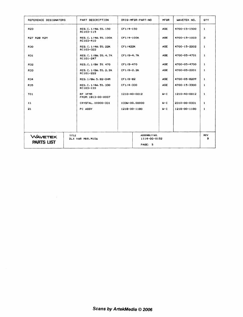
RES, C. 1 /8U . 5 % ~ 4 . 7 K R C l O l - 2 4 7
1 RES. C. 1/BW 5% 4 7 0
REFERENCE DESIGNATORS
RES, C. i / B U , 5%. 2 . 2 K R C l O l - 2 2 2
ORIG-MFGR-PART-NO PART D E S C R I P T I O N
R F XFMR FROM: 1 8 1 3-00-0007
CRYSTAL. X X 0 0 0 - 3 3 1
AS€
ASE
ASE
ASE
ASE
ASE
ASE
ASE
W-I
W-I
W-I
MFGR UAVETEK NO.
I ASSEMBLY NO.
1 1 1 4 - 0 0 - 0 1 5 2 wAvE~EK PARTS LIST I PAGE: 5
TITLE D L X H A R M K R , M 1 0 6
QTY
REV
B
Scans by ArtekMedia O 2006

REFERENCE D E S I G N A T O R S P A R T D E S C R I P T I O N
C A P * ELECT, I M F I 2 5 V C E l 2 O - 0 0 1
CAP, CER. 3 .3PF . 1 K V C D 1 0 1 - R 3 3
CAP. CERn . O l M F , 1 0 0 V C D 1 0 3 - 3 1 0
CAP, VAR, 3 . 5 - 1 3 P F 2 5 0 V C V 1 0 1 - 0 1 3
CAP, CER, 3 6 0 P F . 1 K V C D 1 0 2 - 1 3 6
CAP, CER, 4 7 0 P F a 1 K V C D 1 0 2 - 1 4 7
CAP. CERa . OO2MFa 1 K V C D l 0 2 - 2 2 0
CAP. CER' I Z O P F , 1 K V C D l 0 2 - 1 1 2
D I O D E D G l 0 9 - 1 4 0
D I O D E D G 1 0 0 - 8 2 1
D I O D E D G 0 0 0 - 0 0 7
ORIG-MFGR-PART-NO
1 6 2 D 1 0 5 X 9 0 2 5 B C 2
1OTCC-V33
6 8 U 1 0 3 M
1OTCC-V47
7S-TRIKO-02 -3 .5 -13PF
6 0 U 3 6 1 M
6 0 U 4 7 1 M
5 G A D 2 0
6 0 U 1 2 1 M
I N 4 1 4 8
i N 8 2 A G
5082-2800
MFGR
SPR
SPR
MDC
S P R
STR
MDC
MDC
SPR
MDC
F C D
G - I
H-P
WAVETEK TITLE
PC A S S Y ASSEMBLY NO.
1218-00-1180
PAGE: 1
WAVETEK NO.
1510-21-7010
QTY
REFERENCE DESIGNATORS P A R T D E S C R I P T I O N
I C , I C O O O - 0 1 7
I C , I C O O O - 0 1 6
I C , I C O O O - 0 1 2
I C . I C O O O - 0 0 5
CHOKE . 4 7 M H 1 0 % L A 0 0 5 - R 0 4
TORRID . 10 TURN
TRANS Q A 0 5 0 - 5 3 0
TRANS O A 0 5 4 - 5 8 0
TRANS Q A 0 5 4 - 6 1 0
RES. 1 /8W. 5. 12K-OHM
RES, Cz 1/4W. 5 % ~ 390 R C l 0 3 - 1 3 9
RES, C, 1 /8W, 5%. 22 R C i O i - 0 2 2
'RES. C' 1 /8W, 5%. 47 R C l O i - 0 4 7
RES. C. 1 /8W 5% 470
ORIG-MFGR-PART-NO
C F i /8-22
MFGR / WAVETEK NO.
S I G
S I C
T - 1
RAY
A S E
H Y T
A P X
MOT
MOT
A S E
A S E
A S E
A S E
A S E
QTY
ASSEMBLY NO.
1218-00-1180 W-TEK PARTS LIST 1 PAGE: 2
TITLE
P C A S S Y REV
D
I I I I I
Scans by ArtekMedia O 2006

I REFERENCE DESIGNATORS I P A R T D E S C R I P T I O N I OR IG-MFGR-PART-NO I MFGR
RES. C, 1 /4W. 5x4 560 RC 103-1 5 6
RES. C, 1/4W, 5%. 180 R C 1 0 3 - 1 1 8
POT. 2 0 K . R P 1 4 4 - 3 2 0
RES, C, 1 /4W8 5 % ~ 1 K R C l 0 3 - 2 1 0
RES, C J 1/8W, 5%' 4 . 7 K R C i O i - 2 4 7
RES, C, 1 /8W, 5x8 2 2 K R C l O i - 3 2 2
RES. Ca 1/8W. 5%. 1OM R C I O I - 6 1 0
RES. C, 1 /4W. 5%. 1 .5K R C 1 0 3 - 2 1 5
RES. C, 1 /8W, 5%, 2 K R C i O i - 2 2 0
RES. C, 1 /4W. 5%. 2 2 K RC 103-322
WAVETEK PARTS LIST
TITLE
PC ASSY
C F l /4-560
C F 1 / 8 - 4 . 7 K
C F l / 8 - 2 2 K
A S E
A S E
A S E
B E K
A S E
A S E
A S E
A-B
A S E
A S E
A S E
I ASSEMBLY NO.
1218-00-1180
I W E T E K NO. :Ty
4 7 0 0 - 0 5 - 1 0 0 1
4700-1 5 - 5 6 0 0
Scans by ArtekMedia O 2006
REFERENCE DESIGNATORS
R 1 4 7 R 1 4 8
R 1 4 9
R 1 5 0
T i 0 1 T i 0 2
TITLE
WAVE'TEK NO.
4 7 0 0 - 1 5 - 1 0 0 2
4700-05-3300
4700-15-1005
1210-40-0016
P A R T D E S C R I P T I O N
RES, C. 1 / 4 W $ 5%, 1OK R C i 0 3 - 3 1 0
RES. 1 /8W, 5 ,330 -OHM
RES, C, 1 /4W, 5%, 1OM R C 1 0 3 - 6 1 0
R F XFMR FROM: 1813-00-0007
Q T Y
2
1
1
2
REV
D WAVETEK PARTS LIST
ORIG-MFGR-PART-NO
C F I /4-1OK
C F l /8-330
C B 1 0 6 5
1 2 1 0 - 4 0 - 0 0 1 6
MFGR
A S E
A S E
A-B
W-I
P C A S S Y ASSEMBLY NO. 1218-00-1180
PAGE: 4

SECTION 7 SCHEMATICS
7.1 INTRODUCTION matics. Additional notes pertaining to specific schematics are included on each schematic i f required.
This section contains all schematics for the instrument. A schematic index is given in Section 7.3. Unless otherwise noted, resistor values are given in ohms,
7.2 SCHEMATIC NOTES capacitor values are given in pF, and inductor values are given in pH.
The following notes and abbreviations pertain to all sche-
SYMBOL NOTES
[/ Denotes DC voltage reading unless otherwise -a Coaxial jack specified.
. ----2) Coaxial plug Denotes high-impedance crystal detector reading in volts unless otherwise specified. Coaxial cable
Denotes 50 ohm crystal detector reading in # Factory adjusted part. volts unless otherwise specified.
Denotes a front-panel device. ------.ojt, Signal or voltage source.
Denotes a rear-panel device.
, - Connects to indicated signal or voltage I C source. , ,;, ,,, , Denotes a printed circuit board adjustment
L.C. V ', L, or accessible module adjustment.
Arrow indicates clockwise rotation of wiper. Denotes an internal module adjustment not accessible without removing module cover.
ABBREVIATION CODE
A AC C CCW
C R C W CW
dB dBc d Bm dBmV DC DS F
F.P. H Hz I C
ampere alternating current capacitor counterclockwise diode continuous wave clockwise deci be1 dB referred to carrier dB referred to 1 mW dB referred to 1 mV direct current indicating device, lamp farad front panel henry hertz integrated circuit
IF J K kHz kL-2 kV kW L M MHz M a m A mH mV mW
PF PA pH
intermediate frequency jack relay kilohertz kilohm kilovolt kilowatt inductor meter megahertz rnegohrn milliampere millihenry millivolt milliwatt microfarad microampere microhenry
n OC P
P
PP P F Q R R F R MS R.P. S T T.P. v V A W X
ohm opto-coupler
plug peak peak-to-peak picofarad transistor resistor radio frequency root-mean-square rear panel switch transformer test point volt voltampere watt crystal
Scans by ArtekMedia O 2006

7.3 SCHEMATIC INDEX
The schematics appear in the following order.
ASSEMBLY NAME
Wiring Diagram Marker System Diagram Power Supply Sweep Rate Sweep Drive Sweep Drive Leveler Marker Adder Sweep Oscillator 1 Sweep Oscillator 2A, 26.3 Output Amplifier Modulator Band Select Interface External Marker Harmonic Marker (1 MHz) Harmonic Marker (5-50 MHz) Single Frequency Marker Deluxe Harmonic Marker
Printed circuit board layouts, where applicable, are shown opposite their corresponding schematics.
Scans by ArtekMedia O 2006
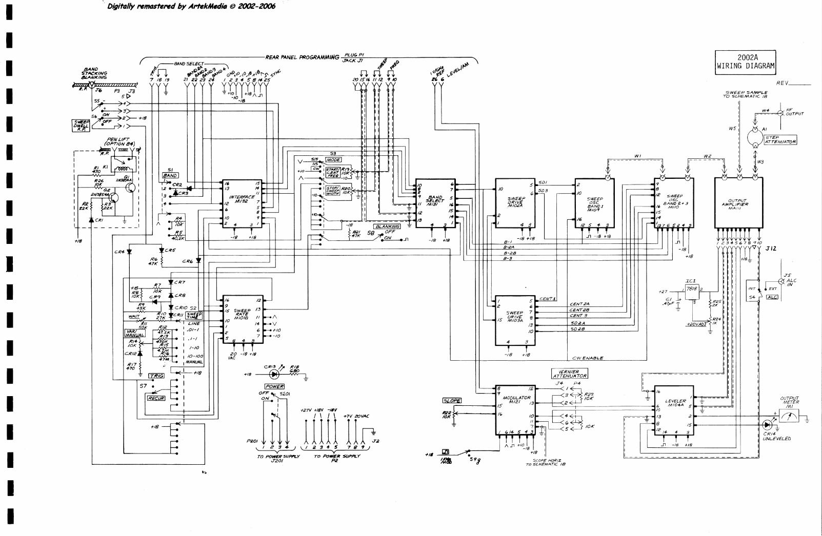


Scans by ArtekMedia O 2006

DPSZA
,?Lv& POWER SUPPLY
1 GND

Scans by ArtekMedia O 2006

MANUAL
SLOW SWEEP
I R I - 1 REV B 1 & R / 7 RIB
R 2 Z O K
(?z?) C 1 8
6.8.. ,, v'" -A)
NEG. R A M P
- C /
/O . 6.8
C t / C'* :; 7
-10"
HYS TFRICS/S
T 6.8 OUTPU 7 . . C 6
C 8
. # R # / R / / , R ~ ~ / R A + , R 3 6 / w , 4 a w7cMfD srs
b< tn

Scans by ArtekMedia O 2006

for, RAMP
NF G RAMP
Scans by ArtekMedia O 2006

R 72 R 7 1 I R 6 7 I 1-1
R W U A 1 a10 1
1 ZR10 CRl!
Scans by ArtekMedia O 2006

REV-
Scans by ArtekMedia O 2006

Scans by ArtekMedia O 2006

LEVELER
Scans by ArtekMedia O 2006
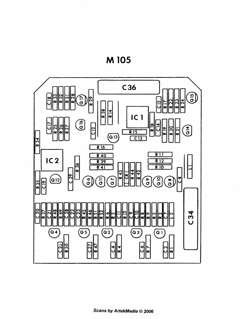
Scans by ArtekMedia O 2006

MARKER ADDER r"l"l
Scans by Artekhledia O 2006

SWEEP OSC. 1 m 0 REV -
n 8-/

SWEEP OSC. 2A, 2R, 3 r .. - B REV-
- .

SHEEP [ OUTPUT AMP 1 SAMPL h
our J Z ) r X REV -
C
R32/ /oA!
q3/2 2 N 5 3 0 6
P 30/
A - + 2 O v 8 - 5 5 . M O N l T C J R O U T P V 7
S S L E V E L E P / N P U T C R . E L E V E L E R / N P U T
C O M P DIODE
9 "1' ~ 5 3 4 G R F M O N I T O P nor^/^
270

Scans by ArtekMedia O 2006

MODULATOR r--1
Scans by ArtekMedia O 2006


I-,
Scans by ArtekMedia O 2006

INTERFACE El
Scans by ArtekMedia O 2006

EXT. MARKER rn MARKER SWEEPSAMPLE
//vpuT / N OUT
R/ 47
BIRD Y OUTPUT
+/8
+/€3 V
Scans by ArtekMedia O 2006
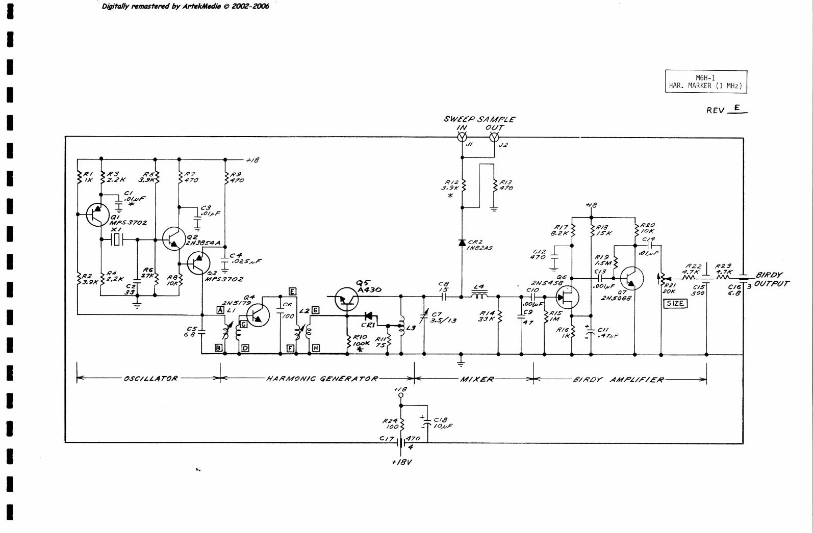
OSC/L L R T O R -4 HARMON/C GENERA T O R - --.< MIXER B/RDY RMPL/F/ER
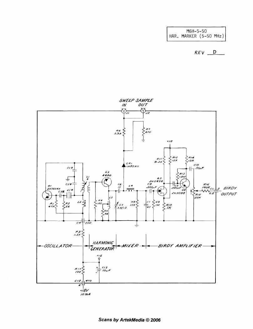
M6H-5-50 HAR. MARKER (5-50 MHz) I
R E V D
Scans by ArtekMedia O 2006

R E V
1S.F. MARKER I
S W E E P SAMPLE
Scans by ArtekMedia O 2006

Scans by ArtekMedia O 2006
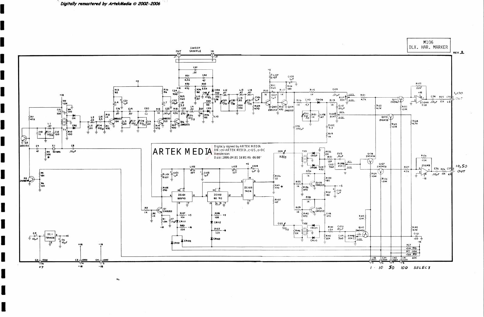
SWEEP
piiq DLX. HAR. MARKER
OUT SAMPLE IN I REVL
I JI
1 6 I

MANUAL CHANGES - MODEL 2002A
1500 MHz crossover ad j . i s R63, n o t R64.
R17 and R45 are now CTS, 363T105B, Wavetek P/N 4610-00-3105.
R10 and R29 a re now 100 kohm, Wavetek P/N 4700-15-1003. R30 and R41 (see schematic d e t a i l s ) a re 1 Mohm potent iometers, CTS, 363S105B, Wavetek P/N 4610-00-1105.
Also, add L1 (Wavetek P/N 1810-05-0004) t o t h e Par ts L i s t .
Page 5-14 Figures 5-20 and 5-21 a r e reversed. F igure 5-20 (M104A Adjustments) i s updated as shown. (NOTE: RF Bal and S.S. Bal a re f a c t o r y adjustments. )
Add 10K r e s i s t o r K43 (Wavetek P/N 4700-15-1002) from p i n 2 o f I C 1 t o ground.
L l O Z ---- c R I I Z L103 - - -- Add CR112 (1N4148, Wavetek
-
P/N 4807-01 -091 4 ) as shown. I I I
Scans by ArtekMedia O 2006