Water-resistant exible GaN LED on a liquid crystal polymer …fand.kaist.ac.kr/Attach/Flexible GaN...
12
Author's personal copy journal homepage: www.elsevier.com/locate/nanoenergy Available online at www.sciencedirect.com RAPID COMMUNICATION Water-resistant flexible GaN LED on a liquid crystal polymer substrate for implantable biomedical applications Sang Yong Lee a , Kwi-Il Park a , Chul Huh b , Min Koo a , Hyeon Gyun Yoo a , Seungjun Kim a , Chil Seong Ah b , Gun Yong Sung b,n,1 , Keon Jae Lee a,nn,1 a Department of Materials Science and Engineering, Korea Advanced Institute of Science and Technology (KAIST), 291 Daehak-ro, Yuseong-gu, Daejeon 305-701, Republic of Korea b Biosensor Research Team, BT Convergence Technology Research Department, Electronics and Telecommunications Research Institute (ETRI), 138 Gajeong-dong, Yuseong-gu, Daejeon 305-700, Republic of Korea Received 25 June 2011; received in revised form 9 July 2011; accepted 9 July 2011 Available online 21 July 2011 KEYWORDS Flexible GaN LED; White LED; Biosensor; PTFE; Liquid crystal polymer substrate Abstract A flexible GaN light-emitting diode (LED) has been fabricated on a liquid crystal polymer (LCP) substrate for biomedical applications. The bending radius and fatigue tests demonstrated the mechanically and optically stable characteristics of the GaN LEDs on the flexible substrates. A white light-emitting phosphor-coated GaN LED showed its potential as a next-generation flexible light source. A water-resistant and biocompatible polytetrafluoroethylene (PTFE) coated flexible LED detected prostate-specific antigen (PSA), which is expected to be used in future biomedical devices. & 2011 Elsevier Ltd. All rights reserved. 1. Introduction Light-emitting diodes (LEDs) have superior characteristics, such as long-term stability, high efficiency, and strong brightness compared to conventional incandescent lamps. With these advantages, LEDs have been developed and explored for not only consumer electronics such as energy efficient light lamp, back-light unit (BLU), and active matrix organic LED (AMOLED) but also medical applications, including body composition detectors (e.g., hemoglobin [1], human body fat [2], prostate- specific antigen (PSA) [3], and cholesterol [4]), and therapy devices (e.g., sterilization [5], skin homeostasis [6], and operation lamps [7]). In particular, flexible LEDs, which can conformally contact on curvilinear surface, have intrigued researchers in the field of biosensors and micro-sized surgery robots for non-bleeding diagnoses and treatment. 2211-2855/$ - see front matter & 2011 Elsevier Ltd. All rights reserved. doi:10.1016/j.nanoen.2011.07.001 n Corresponding author. Tel.: +8242 860 5698; fax: +8242 860 6594. nn Corresponding author. Tel.: +8242 3503343; fax: + 8242 350 3310. E-mail addresses: [email protected] (G.Y. Sung), [email protected] (K.J. Lee). 1 These corresponding authors have equally contributed. Nano Energy (2012) 1, 145–151
Transcript of Water-resistant exible GaN LED on a liquid crystal polymer …fand.kaist.ac.kr/Attach/Flexible GaN...

Author's personal copy
journal homepage: www.elsevier.com/locate/nanoenergy
Available online at www.sciencedirect.com
RAPID COMMUNICATION
Water-resistant flexible GaN LED on a liquid crystalpolymer substrate for implantablebiomedical applications
Sang Yong Leea, Kwi-Il Parka, Chul Huhb, Min Kooa, Hyeon Gyun Yooa,Seungjun Kima, Chil Seong Ahb, Gun Yong Sungb,n,1, Keon Jae Leea,nn,1
aDepartment of Materials Science and Engineering, Korea Advanced Institute of Science and Technology (KAIST),291 Daehak-ro, Yuseong-gu, Daejeon 305-701, Republic of KoreabBiosensor Research Team, BT Convergence Technology Research Department, Electronics and TelecommunicationsResearch Institute (ETRI), 138 Gajeong-dong, Yuseong-gu, Daejeon 305-700, Republic of Korea
Received 25 June 2011; received in revised form 9 July 2011; accepted 9 July 2011Available online 21 July 2011
KEYWORDSFlexible GaN LED;White LED;Biosensor;PTFE;Liquid crystal polymersubstrate
AbstractA flexible GaN light-emitting diode (LED) has been fabricated on a liquid crystal polymer (LCP)substrate for biomedical applications. The bending radius and fatigue tests demonstrated themechanically and optically stable characteristics of the GaN LEDs on the flexible substrates.A white light-emitting phosphor-coated GaN LED showed its potential as a next-generationflexible light source. A water-resistant and biocompatible polytetrafluoroethylene (PTFE)coated flexible LED detected prostate-specific antigen (PSA), which is expected to be used infuture biomedical devices.& 2011 Elsevier Ltd. All rights reserved.
1. Introduction
Light-emitting diodes (LEDs) have superior characteristics, suchas long-term stability, high efficiency, and strong brightness
compared to conventional incandescent lamps. With theseadvantages, LEDs have been developed and explored for notonly consumer electronics such as energy efficient light lamp,back-light unit (BLU), and active matrix organic LED (AMOLED)but also medical applications, including body compositiondetectors (e.g., hemoglobin [1], human body fat [2], prostate-specific antigen (PSA) [3], and cholesterol [4]), and therapydevices (e.g., sterilization [5], skin homeostasis [6], andoperation lamps [7]). In particular, flexible LEDs, which canconformally contact on curvilinear surface, have intriguedresearchers in the field of biosensors and micro-sized surgeryrobots for non-bleeding diagnoses and treatment.
2211-2855/$ - see front matter & 2011 Elsevier Ltd. All rights reserved.doi:10.1016/j.nanoen.2011.07.001
nCorresponding author. Tel.: +8242 860 5698;fax: +8242 860 6594.
nnCorresponding author. Tel.: +8242 350 3343;fax: +8242 350 3310.
E-mail addresses: [email protected] (G.Y. Sung),[email protected] (K.J. Lee).
1These corresponding authors have equally contributed.
Nano Energy (2012) 1, 145–151

Author's personal copy
Organic LEDs (OLEDs) have been studied actively over thelast two decades with the feasibility of flexible devices[8–12]. However, OLEDs have drawbacks such as shortlifetime (�10,000 h) [13] low efficiency, low brightness,and low stability in humidity condition compared toinorganic LEDs (ILEDs) [14,15]. Although the first flexibleGaN materials were demonstrated in 2005 by the author[16], the first flexible III–V LEDs were presented by Kimet al. using micro-structured GaAs (ms-GaAs) [17–20]. Theirms-GaAs LEDs printed on a polyethylene terephthalate (PET)substrate were applied to detect glucose concentrationsfrom the variation of transmitted light intensities. However,the GaAs-based LED, which emits only infrared and red light,ultimately limits the possible applications due to its narrowwavelength range. Recently in 2011, Kim et al. establishedthe flexible GaN ILED by micro-structure transferring process[21]. Although they proposed the feasibility for flexible LEDapplications in display, it did not provide the opportunity forbiomedical devices.
Herein, for the first time, single crystal micro-structuredGaN (ms-GaN) was employed for the water-resistance andbiomedical applications. The superb properties of the GaNmaterial in terms of its wide band gap and high efficiencyenable the dramatic extension of not only consumerelectronic applications (13 billion dollar market of GaNitself in 2011) [22] but also the biosensing scale [23–28].In this study, we describe four works on flexible ILEDs, asfollows: (1) establishment of the flexible GaN ILED that canbe applied to full color RGB elements [24] and controllablemicro-patterned LED arrays; (2) a flexible white LED createdthrough a combination of a blue GaN LED and yellowphosphor, which can be utilized for the promising flexibleBLU [25]; (3) a water-resistant and flexible GaN LED on aliquid crystal polymer (LCP) substrate packaged bybiocompatible polytetrafluoroethylene (PTFE), promisingcandidate materials that enables robustness in body-implanted conditions [29], and (4) diagnosis of diseases(e.g., PSA) by detecting antigen–antibody reactions usingthe flexible GaN LED and photodiode.
2. Results and Discussion
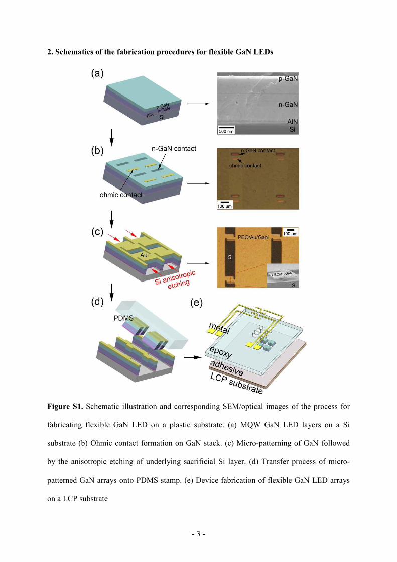
Figs. 1a and S1 illustrate a schematic structure and thefabrication steps of ms-GaN LED arrays settled on a plasticsubstrate with the related scanning electron microscopy(SEM)/optical images. GaN LED epitaxial layers wereaccumulated on a Si (1 1 1) substrate by metal organicchemical vapor deposition (MOCVD; Fig. S1a). The annealingat 600 1C of Au/Cr layers stacked on n-/p-GaN as contactpads enabled the formation of ohmic contact (Fig. S1b).The deposited GaN LED layers were then transferred onto aLCP (Vecstar Series, Kuraray Co., Ltd.) substrate by means ofconventional micro-fabrication and soft lithographic tech-niques (Fig. S1c and d) [26,30]. The LCP has drawn attentionto biomedical research society as an implantable packagingmaterials due to its mechanical stability, low waterabsorption rate (less than 0.04%, comparable to PTFE),excellent chemical resistance, and high transition temp-erature compared to other conventional polymer substrates[29,31–33] (e.g., polyimide, PET) as shown in Table S1 [34].Recent paper from Kim’s group demonstrated that in vitro
accelerated soak tests with the all-LCP monolithicallypackaged devices showed a leakage current sustained atmuch lower value (5.3–16.6 nA at 75 1C) for 300 dayscompared to conventional polyimide and parylene-Cencapsulations [29]. To our knowledge, LCP application asa flexible substrate for high performance semiconductordevices has not been previously reported and it is interestingto note that the biocompatible LCP substrate can withstandthe relatively high temperature process up to �300 1C,which is essential qualification of the high performancedevices on plastics. Finally, a 2� 2 array of metal electrodeswas placed on top of the transferred GaN LED (Fig. S1e). The
Figure 1 (a) Schematic illustration of our flexible GaN LEDarrays on a LCP substrate. (b) Photograph and magnified opticalimage of the 2� 2 GaN LED arrays (each 100� 100 mm2 patternsize) on plastics. The inset indicates electrodes (Au) and activeGaN LED devices. The electrodes 1 and 2 on the LED device areconnected in series with 3 and 4, respectively. (c) EL spectracomparison before and after transferring of micro-structuredGaN LEDs onto LCP substrates.
S.Y. Lee et al.146

Author's personal copy
electrodes were connected to an external source-meter(Keithley 2612A) to turn on the LEDs. Fig. 1a shows theschematic illustration of our flexible 2� 2 GaN LED arrays(Each 100� 100 mm2 pattern size) on a LCP substrate.Lighted 2� 2 arrays of LEDs (Input current=2 mA) rolled upon a cylindrical aluminum rod are displayed in Fig. 1b. Theinset of Fig. 1b is a magnified image of the active region of thelighted GaN LED. Metal electrodes 1 and 2 were connected inseries with 3 and 4, respectively. The electroluminescence (EL)spectra of GaN LED were measured before and aftertransferring onto a LCP substrate. A slight difference of thewavelength peaks, which might be caused by transfer process,is observed in Fig. 1c.
Fig. 2a and b presents the GaN LED simulation results ofthe radiative recombination rate and EL intensity spectrumusing Technology Computer Aided Design (TCAD, Silvaco)software. For the III–V LED simulation, we used Shockley–Read–Hall (SRH)/Auger recombination, Lorentzian gain, andChuang’s band model to calculate InGaN/GaN multi-quantumwell (MQW) optical properties [35]. The MQW recombination
rate (s�1 cm�3) is computed in the magnified region of Fig. 2ainset. The EL comparison between our fabricated flexible GaNLED and TCAD simulation indicates that our flexible LED emitsthe blue light as simulation based on In0.17Ga0.83N MQWstructures shown in the cross-sectional schematic image ofFig. S2.
The electroluminescence (EL) spectra and the I–V curveswere measured at various bending radii, as shown in Fig. 3. Withthe change from flat to about 2.1 mm, degradation did notappear, as shown in Fig. 3a and b. The strain values werecalculated using the equation in our previous papers [16,36].These results demonstrate that our flexible GaN LED maintainedmechanical stability on the flexible LCP substrates andpreserved its optical and electrical properties. Fig. 3b shows
Figure 2 (a) TCAD simulation of the radiative recombinationrate in GaN MQW structure. (b) EL comparison between ourfabricated flexible GaN LED and TCAD simulation. This resultindicates that our flexible LED emits the blue light as TCADsimulation based on In0.17Ga0.83N MQW structures shown in thecross-sectional schematic image of Fig. S2.
Figure 3 (a) EL spectra in various bending radii. (b) I–V curvecharacteristics for various bending radius of high-temperatureannealed ohmic contact (at 600 1C) and non-ohmic contact LEDdevices without annealing. (c) Bending fatigue test (BFT) resultsup to 2000 times. The inset shows photograph of mechanicalBFT on a bending stage.
Flexible GaN LED for implantable biomedical applications 147

Author's personal copy
the electrical properties of ohmic- and non-ohmic contact GaNLEDs on LCP substrates. The turn-on voltage of the ohmiccontact flexible LED is 5.6 V at 0.1 mA, which is lower than thatof the non-ohmic LED (14 V, 0.1 mA). This low voltage operationof our flexible GaN LED is due to the low energy junction barrierbetween the GaN and metals caused by the high-temperatureohmic formation before the transfer to the flexible substrates.Video S1 and Fig. 3c show that the electrical property of theflexible GaN LED does not change during the bending fatiguetest (BFT) at a bending radius of 3.5 mm. No electrical damagewas observed in a harsh cycling condition up to 2000 times on astage, as shown in the inset of Fig. 3c.
Supplementary material related to this article can befound online at doi:10.1016/j.nanoen.2011.07.001.
Fig. 4a shows a schematic of a flexible white LEDstructure composed of a flexible blue GaN LED and yellowYAG:Ce phosphor. YAG:Ce is known to be optically excited byblue light at a wavelength of 460 nm, then emitting ataround 550 nm [37]. In the inset of Fig. 4b and Video S1, theflexible white LED is demonstrated; it is activated by aphosphor coating mixed with transparent epoxy resin on theblue LED active region. As shown in Fig. 4b, two distinctemission bands from the flexible GaN LED and YAG:Cephosphor are clearly divided at 440 nm and at approximately540 nm, respectively. At 440 and 540 nm, the emissionintensities increase with an increase in the current from0.1 to 1 mA, as expected. Fig. 4c presents a comparison ofthe Commission International de l’Eclairage (CIE) 1931chromaticity coordinates. The CIE color coordinates of ourflexible blue GaN LED and of the white LED were (0.194,0.074) and (0.332, 0.241), respectively. This approachverifies that our GaN-based white LED has the potential tobe applied as a flexible white light source for BLU and in vivobiodevices [25,38].
The water-resistance of the GaN LED was evaluated, asshown in Fig. 5. A soaking test was conducted with apolytetrafluoroethylene (PTFE, JET protect) coated GaN LEDbuilt on a LCP substrate in a phosphate buffer saline (PBS,pH 7.4) solution mixed with black ink (Video S1 and Fig. 5a(i, ii)). PTFE is a biocompatible material with surgicalapplications, such as artificial blood vessels or felt due to itsnon-sticking, non-wetting, and chemical-resisting properties[39,40]. The I–V curves shown in Fig. 5b indicate that theelectrical properties do not alter, even after soaking in PBSfor 2 days.
Fig. 6a shows the schematics of the PSA sensingmechanism in the LED biochip. The fabrication process ofthe PSA reaction chip is similar to that introduced in anearlier paper by the authors [3]. Polystyrene 96-wellmicrotiter plates (Nunc) were coated with a 5 mg/mLmonoclonal anti (mab)–PSA solution (Fitzgerald) in 1� PBSfor 2 h. This was followed by blocking of the unreacted platewith casein as a blocker (Fig. 6a (i)). PSA antigen solutions(Fitzgerald, 1�PBS) of various concentrations from 1 to100 ng/ml were added to the mab-PSA coated plates (Fig. 6a(ii)), causing a specific binding reaction. Polyclonal anti(pab)–PSA–Au nanoparticle (NP) conjugates were capturedon the microtiter plates using a sandwich-type immunogoldassay, which led to a specific reaction between the pab–PSA–Au NPs and the fixed target PSA antigen on the surface. Toincrease the light blocking effects from NPs immobilized onthe surface, Ag staining was performed on the Au NPs for
12 min (Fig. 6a (iii)) [41]. The measurement moduleconsisted of three parts: a flexible GaN LED for the opticalinput, an electroluminescence detector, and a reaction chip
Figure 4 (a) Schematic image of the flexible white LEDcomposed of a flexible blue GaN LED and yellow YAG:Cephosphor. (b) EL data of the flexible white LED. The inset imageshows the bended white LED. (c) The CIE color coordinates of theflexible (i) blue GaN LED and (ii) phosphor-coated white GaN LED.
S.Y. Lee et al.148

Author's personal copy
with biomolecules immobilized on the glass surface. Fig. 6bshows the PSA reaction chip surface. The white dots in areaction chip are biomolecules immobilized on the glasssurface, which increased with increasing the PSAconcentration. Fig. 6c shows the integrated EL intensity ofthe flexible LED as a function of the PSA concentrationranging from 1 to 100 ng/mL. The integrated EL intensity ofthe flexible LED biosensor decreases with an increase in thePSA concentration, as clearly shown in Fig. 6c. The numberof immunogold NPs increased as the concentration of thePSA concentration increased. Therefore, as more PSA con-centration is added, less transmitted light that passes fromthe flexible LED through the reaction chip is detected. Theinset of Fig. 6c shows the EL spectra as a function of the PSAconcentration at a constant current of 0.5 mA. The limit ofdetection (LOD) of the PSA used in this experiment wasestimated to be approximately 1 ng/mL, promising forprostate cancer screening between a healthy person and apatient at a concentration of 4 ng/mL PSA. This type offlexible LED biosensor system can be used for diagnosingdiverse cancers; for the continuous monitoring of glucose,cholesterol, and hemoglobin; and for the detection ofvarious biomolecules of relevance for biomedical devices.A label-free biomolecule detection method with flexibleGaN LEDs and photodiodes will be our future work forpromising implantable biosensors. For example, because thecholesterol in the whole blood has a wave band of 455–475 nm, it can be directly detected using flexible GaN LED
and photodiode without any other pretreatment such as anantibody immobilization.
3. Summary
In summary, we fabricated the nitride-based flexible LED ona LCP substrate for the first water-resistance and biosensorapplications. A bending test of the radius up to 2.1 mm and
Figure 5 (a) PBS soaking test images of the PTFE-coatedflexible LED. (b) I–V curve results of the soaking test. The I–Vcurves indicate that the electrical properties do not alter, evenafter soaking in PBS for 2 days.
Figure 6 (a) Schematics of the PSA sensing mechanism in LEDbiochip. (b) SEM images of the PSA reaction chips. (c) Area of ELintensity as a function of serum PSA concentrations. The inset showsthe dependence of the EL intensity on the PSA concentrations.
Flexible GaN LED for implantable biomedical applications 149

Author's personal copy
a cycling test up to 2000 times demonstrated that our flexibleGaN LED is mechanically and optically stable on flexiblesubstrates. The flexible white LEDs demonstrate thefeasibility of using a white light source for future flexibleBLU display and an implantable micro-sized robot. Usingwater-resistant and biocompatible PTFE-coated flexible LEDbiosensor, the PSA at a limit of 1 ng/mL was detected byemploying the antibody–antigen reaction and Au nanoparti-cles stained with silver for the signal amplification. Theseresults show that the nitride-based flexible LED can be usedas a type of LED display and biosensors.
4. Experimental section
4.1. Growth of GaN LED epitaxial layers on aSi (1 1 1) substrate
The GaN LED epitaxial layers were made up of In0.17Ga0.83Nmulti-quantum well (MQW) structures, InGaN/GaN under-lying superlattices (SLs), cladding layers, and buffer layersgrown on a Si (1 1 1) substrate.
4.2. Forming the ohmic contact pads
For the n-GaN ohmic contact, n+-(In)GaN/p-(In)GaN/MQW/SLs/n-GaN stacks were etched by an inductively coupledplasma reactive ion etcher (ICP-RIE, 25 mTorr, 5 sccm Ar/100 sccm Cl2, 400 W power/150 W bias, 90 s) until the n-GaNlayer was exposed. Au/Cr layers (40 nm/5 nm in thickness)were deposited on both the n-GaN and n+-(In)GaN/p-(In)GaN layers to serve as the n and p ohmic contactpads, respectively. The ohmic contact pads were annealedat 600 1C in N2 ambient for 1 min via rapid thermalannealing (RTA).
4.3. Freestanding the GaN LED layers afterremoval of the underlying Si sacrificial layer
To protect the ohmic contact pads, PEO (plasma-enhancedchemical vapor deposited-SiO2, 400 mTorr, 20 sccm 9.5% SiH4,10 sccm N2O, 300 1C, 20 W)/Au/Cr (1 mm/200 nm/10 nm inthickness) mask was additionally deposited onto the contactpads. The PEO layer (ICP-RIE etching, 25 mTorr, 50 sccm CF4,150 W power/40 W bias, 25 min) and the Au (wet etchingfor 1 min, Gold etch, Transene Co.) were patterned usingthe conventional photolithography and etching techniques.Chlorine-based ICP-RIE (25 mTorr, 5 sccm Ar/100 sccm Cl2,400 W power/150 W bias, 25 min) etched then the exposedGaN LED structure under the PEO/Au/Cr etch mask with a100� 100 mm narrow-bridge pattern. During the ICP-RIE dryetching process, the PEO mask layer was etched away by high-density plasma. Anisotropic wet etching by potassium hydro-xide (KOH, 20.0 wt%, 75 1C, 25 min) removed the underlying Silayer and separated the GaN LED layers (narrow-bridge patternof 100� 100 mm2) from the mother substrate. During thishighly concentrated alkaline etching process, a protecting Aumask served to prevent the ohmic contact pads fromdegrading.
4.4. Transfer of the GaN LED layer
A polydimethylsiloxane (PDMS, Sylgard 184, Dow Corning)stamp was uniformly contacted with the Au masked ms-GaNlayers. Upon fast removal from the mother substrate, thenarrow-bridge-shaped ms-GaN LED was completely trans-ferred onto the PDMS stamp. Polyurethane (PU, Norlandoptical adhesive, No. 73) was coated onto liquid crystalpolymer (LCP, Kuraray Co., Ltd., 25 mm in thickness)substrates as a terminus of the GaN LED. The substrateholding the GaN LED was indurated with ultraviolet (UV)light to optically cure the PU. Finally, the GaN LED layerswere shown to be attached well to the LCP substrate whenthe PDMS stamp was removed.
4.5. Fabrication of a 2�2 array flexible GaN LED
A UV-sensitive epoxy (SU8-5) was spin-coated on top of GaNLED/PU/LCP substrates. The metal contact area was thenopened with standard photolithography, and this wasfollowed by a metallization process that consisted ofAu/Cr deposition (RF sputtering, 150 nm/15 nm in thickness)and the formation of a 2� 2 array electrode.
Acknowledgments
This work was supported by the KOCI (grant code: 10ZC1110:Basic Research for the Ubiquitous Lifecare Module Develop-ment) and Basic Science Research Program (grant codes:2010-0028161, CAFDC-2010-0009903) through the NationalResearch Foundation of Korea (NRF) funded by the Ministryof Education, Science and Technology.
Appendix A. Supplementary material
Supplementary data associated with this article can be foundin the online version at doi:10.1016/j.nanoen.2011.07.001.
References
[1] K.J. Jeon, S.J. Kim, K.K. Park, J.W. Kim, G. Yoon, J. Biomed.Opt. 7 (2002) 45.
[2] J.M. Conway, K.H. Norris, C.E. Bodwell, Am. J. Clin. Nutr.40 (1984) 1123.
[3] C.G. Ahn, C.S. Ah, T.Y. Kim, C.W. Park, J.H. Yang, A. Kim,G.Y. Sung, Appl. Phys. Lett. 97 (2010) 103703.
[4] A.M. Scheggi, S. Martellucci, A.N. Chester, R. Pratesi, Biome-dical Optical Instrumentation and Laser-assisted Biotechnology,Kluwer Academic Publishers, 1996 (vol. 325, p. 351).
[5] A. Hamamoto, M. Mori, A. Takahashi, M. Nakano, N. Wakikawa,M. Akutagawa, T. Ikehara, Y. Nakaya, Y. Kinouchi, J. Appl.Microbiol. 103 (2007) 2291.
[6] P. Babilas, M. Landthaler, R.M. Szeimies, Eur. J. Dermatol.16 (2006) 340.
[7] J.-i. Shimada, K. Itoh, M. Nishimura, Y. Kawakami, K. Tsuji,Proc. SPIE 4278 (2001) 165.
[8] X.H. Wang, M. Amatatongchai, D. Nacapricha, O. Hofmann,J.C. de Mello, D.D.C. Bradley, A.J. de Mello, Sensors ActuatorsB-Chem. 140 (2009) 643.
[9] H. Cho, C. Yun, J.W. Park, S. Yoo, Org. Electron. 10 (2009) 1163.
S.Y. Lee et al.150

Author's personal copy
[10] T. Yamamura, M. Kitamura, K. Kuribayashi, Y. Arakawa, S.Takeuchi, in: Proceedings of the IEEE 20th InternationalConference on Micro Electro Mechanical Systems, Kobe, Japan,2007, p. 739.
[11] J.A. Hagen, W. Li, J. Steckl, J.G. Grote, Appl. Phys. Lett.88 (2006) 171109.
[12] T. Sekitani, H. Nakajima, H. Maeda, T. Fukushima, T. Aida,K. Hata, T. Someya, Nat. Mater. 8 (2009) 494.
[13] T. Nakayama, K. Hiyama, K. Furukawa, H. Ohtani, KonikaMinolta Technol. Rep. 5 (2008) 115.
[14] D.A. Gaul, W.S. Rees, Adv. Mater. 12 (2000) 935.[15] F.A. Ponce, D.P. Bour, Nature 386 (1997) 351.[16] K.J. Lee, J. Lee, H.D. Hwang, Z.J. Reitmeier, R.F. Davis,
J.A. Rogers, R.G. Nuzzo, Small 1 (2005) 1164.[17] R.H. Kim, D.H. Kim, J.L. Xiao, B.H. Kim, S.I. Park, B. Panilaitis,
R. Ghaffari, J.M. Yao, M. Li, Z.J. Liu, V. Malyarchuk, D.G. Kim,A.P. Le, R.G. Nuzzo, D.L. Kaplan, F.G. Omenetto, Y.G. Huang,Z. Kang, J.A. Rogers, Nat. Mater. 9 (2010) 929.
[18] J. Yoon, S. Jo, I.S. Chun, I. Jung, H.S. Kim, M. Meitl, E. Menard,X.L. Li, J.J. Coleman, U. Paik, J.A. Rogers, Nature 465 (2010) 329.
[19] S.I. Park, A.P. Le, J.A. Wu, Y.G. Huang, X.L. Li, J.A. Rogers,Adv. Mater. 22 (2010) 3062.
[20] S.I. Park, Y.J. Xiong, R.H. Kim, P. Elvikis, M. Meitl, D.H. Kim, J. Wu,J. Yoon, C.J. Yu, Z.J. Liu, Y.G. Huang, K. Hwang, P. Ferreira,X.L. Li, K. Choquette, J.A. Rogers, Science 325 (2009) 977.
[21] H.S. Kim, E. Brueckner, J. Song, Y. Li, S. Kim, C. Lu, J. Sulkin,K. Choquette, Y. Huang, R.G. Nuzzo, J.A. Rogers, Proc. Natl.Acad. Sci. USA 108 (2011) 10072.
[22] R. Young, Global Manufacturing Trends: What Can We Learnfrom the HB LED Market Explosion?, can be found under, 1999./http://apps1.eere.energy.gov/buildings/publications/pdfs/ssl/young_trends_boston2011.pdfS.
[23] T. Mukai, M. Yamada, S. Nakamura, Jpn. J. Appl. Phys.38 (1999) 3976.
[24] S.J. Pearton, J.C. Zolper, R.J. Shul, F. Ren, J. Appl. Phys.86 (1999) 1.
[25] N. Kijima, Y. Shimomura, T. Kurushima, H. Watanabe,S. Shimooka, M. Mikami, K. Uheda, J. Light & Visual Environ.32 (2008) 202.
[26] K.J. Lee, M.A. Meitl, J.H. Ahn, J.A. Rogers, R.G. Nuzzo,V. Kumar, I. Adesida, J. Appl. Phys. 100 (2006) 124507.
[27] J.H. Ahn, H.S. Kim, K.J. Lee, S. Jeon, S.J. Kang, Y.G. Sun,R.G. Nuzzo, J.A. Rogers, Science 314 (2006) 1754.
[28] M.A. Meitl, Z.T. Zhu, V. Kumar, K.J. Lee, X. Feng, Y.Y. Huang,I. Adesida, R.G. Nuzzo, J.A. Rogers, Nat. Mater. 5 (2006) 33.
[29] S.W. Lee, K.S. Min, J. Jeong, J. Kim, S.J. Kim, IEEE Trans.Biomed. Eng. 99 (2011) 1.
[30] K.I. Park, S. Xu, Y. Liu, G.T. Hwang, S.J.L. Kang, Z.L. Wang,K.J. Lee, Nano Lett. 10 (2010) 4939.
[31] Y. Kumano, Y. Tomura, M. Itagaki, Y. Bessho, Microelectron.Reliab. 41 (2001) 525.
[32] S.W. Lee, J.M. Seo, S. Ha, E.T. Kim, H. Chung, S.J. Kim, Invest.Ophthalmol. Visual Sci. 50 (2009) 5859.
[33] D. Thompson, N. Kingsley, G. Wang, J.M. Papapolymerou, M.Tentzeris, in: Proceedings of the IEEE MTT-S Int. Microw. Symp.Dig. Long Beach, CA, USA, 2005, pp. 857.
[34] (a) /http://www.kuraray.co.jpS. (b) /http://www.matweb.comS.
[35] ATLAS User’s Manual, software version 5.10.0.R, SilvacoInternational, Santa Clara, CA, 2007.
[36] R.S. Yang, Y. Qin, L.M. Dai, Z.L. Wang, Nat. Nanotechnol.4 (2009) 34.
[37] J.K. Park, M.A. Lim, C.H. Kim, H.D. Park, J.T. Park, S.Y. Choi,Appl. Phys. Lett. 82 (2003) 683.
[38] Y. Saeki, K. Takamura, K. Magatani, in: Proceedings of the 28thIEEE EMBS Annual International Conference, New York, USA,2006, pp. 1351.
[39] C. Briguori, J. De Gregorio, T. Nishida, M. Adamian, R. Albiero,G. Tucci, C. Di Mario, A. Colombo, Am. J. Cardiol. 86 (2000) 343.
[40] S. Cillino, L. Zeppa, F. Di Pace, A. Casuccio, D. Morreale,F. Bocchetta, G. Lodato, Acta Ophthalmol. 86 (2008) 314.
[41] S.J. Park, T.A. Taton, C.A. Mirkin, Science 295 (2002) 1503.
Prof. Keon Jae Lee received his Ph.D.degree from the University of Illinois, Urba-na-Champaign, in 2006. During his Ph.D.course at UIUC, he was involved in the firstco-invention of ‘‘High Performance FlexibleSingle Crystal Electronics’’, called micro-structured silicon and GaN. From 2006 to2008, he conducted a joint research projectof Unisantis (Japan) and IME (Singapore) inthe field of three dimensional surrounding
gate nano-transistors (SGT) for the future logic technology. Since2009, he has been an Assistant Professor in MSE at KAIST. His currentresearch interests are flexible and nanobio devices for health, self-powered energy, and electronic applications.
Flexible GaN LED for implantable biomedical applications 151

- 1 -
Supporting Information for:
Water-resistant Flexible GaN LED on a Liquid Crystal Polymer Substrate for
Implantable Biomedical Applications
By Sang Yong Lee, Kwi-Il Park, Chul Huh, Min Koo, Hyeon Gyun Yoo, Seung Jun Kim, Chil
Seong Ah, Gun Yong Sung,* and Keon Jae Lee*
*These corresponding authors have equally contributed.

- 2 -
1. Liquid Crystal Polymer (LCP) properties compared to other polymer substrates
LCP PI PET
Melting Temp. (°C)
315 None 260
Tg (°C) 285 300 75
Water absorption (%) 0.04 2.9 0.5
Dielectric Constant (1 MHz)
3.0 3.1 3.0
Oxygen transmission
(㎠(STP)/㎡/day, 20-23 °C)
0.03 - 0.09 0.04 - 17 1.7 – 7.7
Water vapor transmission
(g/㎡/day, 37.8-40 °C)
0.006 - 0.016 0.4 - 21 3.9 - 17
Thermal expansion (ppm/°C)
0 - 30 controllable
20 15
Table S1. LCP properties compared to other polymer substrates.[32]
- 3 -
2. Schematics of the fabrication procedures for flexible GaN LEDs
Figure S1. Schematic illustration and corresponding SEM/optical images of the process for
fabricating flexible GaN LED on a plastic substrate. (a) MQW GaN LED layers on a Si
substrate (b) Ohmic contact formation on GaN stack. (c) Micro-patterning of GaN followed
by the anisotropic etching of underlying sacrificial Si layer. (d) Transfer process of micro-
patterned GaN arrays onto PDMS stamp. (e) Device fabrication of flexible GaN LED arrays
on a LCP substrate

- 4 -
3. GaN LED structure on a Si substrate
Figure S2. Schematic illustration of the GaN LED structure.

- 5 -
4. The video of flexible GaN LED operation test
Video S1. The real-time views during the operation test.