
Wafer Products Handling and Operating Manual · 2020-05-23 · Wafer Products Handling and...
16
Wafer Products Handling and Operating Manual(Rev.1.0) Seiko Epson Corporation 1 Wafer Products Handling and Operating Manual This manual describes notes on using Epson Wafer products. It is the responsibility of the customer to optimize the process and the mounting parameters to obtain the optimum results. The content of this document is subject to change without notice.
Transcript of Wafer Products Handling and Operating Manual · 2020-05-23 · Wafer Products Handling and...
Wafer Products Handling and Operating Manual(Rev.1.0)
Seiko Epson Corporation 1
Wafer Products
Handling and Operating Manual
This manual describes notes on using Epson Wafer products. It is the responsibility of the
customer to optimize the process and the mounting parameters to obtain the optimum
results.
The content of this document is subject to change without notice.
Wafer Products Handling and Operating Manual(Rev.1.0)
Seiko Epson Corporation 2
Wafer Products Handling and Operating Manual
Notice using this document:
This document is not intended to define “specifications” or “recommendations” but to introduce
something to note while using the product.
NOTICE
1. This document may not be copied, reproduced, or used for any other purpose, in whole or in part, without
the consent of Seiko Epson Corporation (“Epson”).
2. Before purchasing or using Epson products, check with our sales representative for the latest information.
Always consult Epson web site or other sources for the latest information.
3. Information provided in this document is for reference only. Epson makes no guarantees against any
infringements of or damages to a third party intellectual property rights or any other rights resulting from
the information. Epson does not give any licenses to use the intellectual property rights or any other rights
of a third party or Epson under this document.
4. When using Epson products, evaluate mounting and soldering thoroughly, and use the Epson products
within the guarantee range specified by Epson. Epson shall have no liability for malfunctions, accidents
resulting in injury or death, fire accident or social damages arising out of the use of Epson products beyond
such specified by Epson.
5. Epson has prepared this document carefully and accurately as much as possible, but Epson does not
guarantee that the information presented herein is error-free. Epson assumes no responsibility for any
damages caused by the customers resulting from information errors in this document.
6. Epson products listed in this document and their associated technologies may not be used in equipment or
systems that are prohibited from manufacturing, using or selling under the laws, regulations, or rules in
Japan or any other countries. Furthermore, Epson products or their associated technologies may not be
used for the development, etc., of weapons of mass destruction, for military uses, or other military
applications. If exporting Epson products or their associated technologies, be sure to comply with the
“Foreign Exchange and Foreign Trade Control Act” in Japan, the “Export Administration Regulations (EAR)”
and other export-related laws and ordinances in Japan and any other countries. Also, follow the required
procedures as provided by the relevant laws and ordinances.
7. Epson assumes no responsibility if our products are used in violation of conditions listed in this document
and such use results in damage.
8. For details of environmental compatibility etc. of Epson products, check Epson's web site.
9. Epson assumes no responsibility if our products' failure or characteristic fluctuation occurs due to external
factors (static electricity, overvoltage / overcurrent, thermal stress, mechanical stress, environmental
atmosphere) in the products handling, mounting, and customer's process.

Wafer Products Handling and Operating Manual(Rev.1.0)
Seiko Epson Corporation 3
Table of Contents
1. Outline of Wafer and Bare Die Products.................................................................4
1.1 Wafer Products Structure ......................................................................................5
1.1.1 The Specifications of 6-Inch Wafer Products Dimension........................................5
1.1.2 The Specifications of 8-Inch Wafer Products Dimension........................................5
1.2 Identifications of the Defective dies in Wafer Products................................................6
1.3 Color Unevenness on Wafer Products Back Side.........................................................6
1.4 Bare Die Structure..............................................................................................7
1.5 Examples of Structure by Pad Type......................................................7
2. Handling Precautions for Wafer and Bare Die Products..................................................8
2.1 Introduction........................................................................................................8
2.2 Storage..............................................................................................................8
2.2.1 Packing Type for Wafer Products....................................................................8
2.2.2 Storage Periods of Wafer Products.....................................................................9
2.3 Precautions for Handling operations of Wafer Products ............................................10
2.4 Precautions for Processing and Mounting Wafer Products................................11
2.5 Precautions for Mounting Bare Die ........................................................................11
2.6 Precautions Against the Light Irradiation...................................................11
3. Countermeasures Against Static Electricity in Handling Semiconductor Products...............12
3.1 Working Environment.........................................................................................12
3.2 Storage Environment..........................................................................................12
3.3 Handling...........................................................................................................13
3.4 Equipment and Jig..............................................................................................13
Appendix-1 Procedure that Open the Wafer Products(Wafer Shipping Box)....................14
Appendix-2 Procedure that Open the Wafer Products(Wafer Case)................................15
Revision History...........................................................................................................16

Wafer Products Handling and Operating Manual(Rev.1.0)
Seiko Epson Corporation 4
1. Outline of Wafer and Bare Die Products
Wafer products and Bare Die products are shipped as wafers or diced (singulated) dies
according to the customer’s request in order to realize the mounting on the substrate in the
bare die stated by the customer.
Wafer products are subjected to the process from our wafer production process’s probe
inspection process (electrical characteristics test) and are shipped to customers in wafer state
(after back grinding or no back grinding).
Bare die products which shipped in die state are subjected to back grinding, dicing, placing in
the tray and visual inspection.
Wafer products and bare die products are stored and shipped in shipping containers as
shown.
Fig. 1.3
Wafer Canister
(Wafer Horizontal Type)
Fig. 1.4
Die Tray
Fig. 1.2
Wafer Shipping Box
(Wafer Vertical Type)
Fig. 1.1 Sample Flow: Wafer/Bare Die Products.
Wafer Products Handling and Operating Manual(Rev.1.0)
Seiko Epson Corporation 5
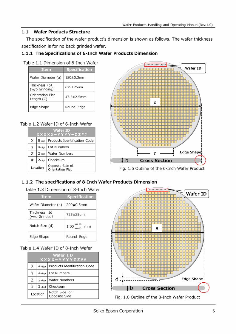
1.1 Wafer Products Structure
The specification of the wafer product's dimension is shown as follows. The wafer thickness
specification is for no back grinded wafer.
1.1.1 The Specifications of 6-Inch Wafer Products Dimension
1.1.2 The specifications of 8-Inch Wafer Products Dimension
Fig. 1.6 Outline of the 8-Inch Wafer Product
Fig. 1.5 Outline of the 6-Inch Wafer Product
Table 1.4 Wafer ID of 8-Inch Wafer
Table 1.1 Dimension of 6-Inch Wafer
Table 1.2 Wafer ID of 6-Inch Wafer
Table 1.3 Dimension of 8-Inch Wafer

Wafer Products Handling and Operating Manual(Rev.1.0)
Seiko Epson Corporation 6
1.2 Identifications of the Defective Dies in the Wafer Products
The defective dies in the wafer products are identified by ink-marking on the die in the Probe
Test Process (Electrical Characteristics Test).
Ink-marks are marked with black color ink. The specifications of the Ink-mark size is shown
in Table 1.5.
Epson will provide wafer map information using electronic data (SEMI standard: xml format)
depending on customer requests. We need to define the specification (e.g. data format, data
transfer methods, etc.) before applying the electronic data, so please contact our sales
representative.
1.3 Color Unevenness on Wafer Products Back Side
In the wafer manufacturing process, an uneven film is formed on the back of the wafer. The
color unevenness may differ from wafer to wafer or within each wafer due to variations of film
thickness, and this does not affect the product functionality and quality.
Fig. 1.9 Color Unevenness on Wafer Back Side
(Micro Visual)
Table 1.5 Ink-Mark Specifications
Fig. 1.8 Color Unevenness on Wafer Back Side
(Macro Visual)
Fig. 1.7 Example: Ink-marks on Wafer products

Wafer Products Handling and Operating Manual(Rev.1.0)
Seiko Epson Corporation 7
1.4 Bare Die Structure
An example of a general structure of our bare die is shown as follows.
1.5 Examples of Structure by Pad Type
Fig 1.12 Al-Pad
(Section View)
大
Fig. 1.14 Au-Bump
(Section View)
Table 1.6 Die Structure and Feature
Description
Fig. 1.13 Au-Bump
(Top View)
Fig. 1.11 Al-Pad
(Top View)
Fig. 1.10 Example Bare Die Structure
Wafer Products Handling and Operating Manual(Rev.1.0)
Seiko Epson Corporation 8
2. Handling Precaution for Wafer and Bare Die Products
2.1 Introduction
Our semiconductor products are designed and manufactured to assure problem-free
operation when used under normal operating conditions. All products are subject to stringent
electrical and mechanical testing to ensure reliability, but users are strongly recommended to
observe the following precautions when designing systems, handling and storing products to
minimize the chance of failure.
Wafer and Bare Die products have a higher risk of quality and reliability degrading
depending on the handling method than general products.
The passivation film applied on wafer and bare die products surface are not design to
protect the die from external impact.
Moisture and dust in the air and careless handling during assembly can cause defective
products, so please take care adequately.
Please perform sufficient evaluations for quality and reliability by the customer: such as
testing and screening to detect failures.
2.2 Storage
Do not induce impact, vibration, or contact with water to prevent damages of bare die.
Do not store or use the products under conditions where moisture condensation may be
formed due to rapid changes in temperature. Also, do not put on load to the product during
storage
When storing, avoid dusty conditions or locations with corrosive gases.
2.2.1 Packing Type for Wafer Products
Wafer products are shipped in Wafer Shipping Box or Wafer Case depending on wafer
diameter and thickness.
When wafer products are shipped, they are stored in wafer shipping box or wafer canister
to prevent damage during transportation. Then the boxes or canisters are packed in antistatic
bags. Do not open the bags more frequent than necessary to prevent foreign material. And
do not leave trays open for prolonged time.
Table 2.1 Packing type of wafer products

Wafer Products Handling and Operating Manual(Rev.1.0)
Seiko Epson Corporation 9
2.2.2 Storage Periods of Wafer Products
After the bags are opened, assemble the products immediately in order to prevent the
bonding degradation caused by the quality change on the bonding pad surfaces.
If products are to store for long period of time, sufficient mounting evaluations (e.g.
bondability evaluation) by the customer is needed.
(Maximum allowable storage periods, including before and after opening
the package, are twelve months under the conditions mentioned.)
Table 2.2 Storage Periods of Wafer Products
Fig. 2.1 Example of Opening the Package (Before and After Opening) of Wafer Products
Wafer Products Handling and Operating Manual(Rev.1.0)
Seiko Epson Corporation 10
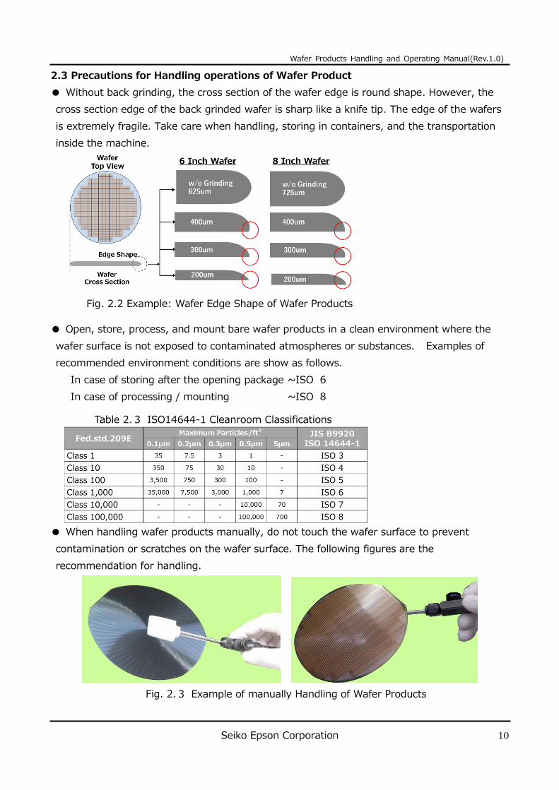
2.3 Precautions for Handling operations of Wafer Product
Without back grinding, the cross section of the wafer edge is round shape. However, the
cross section edge of the back grinded wafer is sharp like a knife tip. The edge of the wafers
is extremely fragile. Take care when handling, storing in containers, and the transportation
inside the machine.
Open, store, process, and mount bare wafer products in a clean environment where the
wafer surface is not exposed to contaminated atmospheres or substances. Examples of
recommended environment conditions are show as follows.
In case of storing after the opening package ~ISO 6
In case of processing / mounting ~ISO 8
When handling wafer products manually, do not touch the wafer surface to prevent
contamination or scratches on the wafer surface. The following figures are the
recommendation for handling.
Fig. 2.3 Example of manually Handling of Wafer Products
Table 2.3 ISO14644-1 Cleanroom Classifications
Fig. 2.2 Example: Wafer Edge Shape of Wafer Products

Wafer Products Handling and Operating Manual(Rev.1.0)
Seiko Epson Corporation 11
2.4 Precautions for Processing and Mounting Wafer Product
When processing and mounting wafer products, perform in a clean environment where it is
not exposed to contaminated atmospheres or substances.
When dicing a wafer, the wafer may be charged up during dicing. Take sufficient
countermeasures against static electricity in the processing.
2.5 Precautions for Mounting Bare Die
When mounting bare die, perform in a clean environment where it is not exposed to
contaminated atmospheres or substances.
Please use the bare die collet for pickup and die bonding. If foreign material adheres to
the collet, process defects such as scratches on the bare die surface may occur. When using
a collet with a surface that comes into contact with the bare die surface, periodic cleaning
should be carried out.
Do not clean bare dies. If bare dies have to be cleaned, extreme precaution must be
carried out to ensure no residue remain on die surface.
When mounting bare die, take sufficient countermeasure against static electricity.
For mold resins, use “semiconductor grade” material. This is recommended to prevent
corrosion in bonding pads due to moisture absorption, and reduce internal stress due to
temperature changes. Similar precautions must be taken for other materials to be used.
2.6 Precautions Against the Light Irradiation
Exposing semiconductor products to the light may have a chance to lead to malfunction, as
the light affects the device characteristics. To prevent products from malfunction, please take
into account the following points regarding semiconductor mounted substrates and products.
During product design and assembly, please consider the product structure so that the
bare die is shielded from light in actual use.
In the testing process, please provide the light-shielded environment for the bare die under
test.
Please consider to shield light from of the surface, back, and sides of the bare die, as bare
die should be shielded from light entirely.
Wafer Products Handling and Operating Manual(Rev.1.0)
Seiko Epson Corporation 12
3. Countermeasures Against Static Electricity in Handling Semiconductor Products
Although all terminals are equipped with an anti-electrostatic circuit, electrostatic beyond the
capacity may lead to break down. So please take sufficient countermeasures when handling
products.
This document introduces examples of basic countermeasures. Please refer to below
guidelines
3.1 Working Environment
It is recommended that the working environment be maintained at a relative humidity of at
least 45%. If the relative humidity is low, the charge diffusivity decreases, and it becomes
easier to charge up.
Lay a conductive layer (conductive mat / conductive sheet) on the floor and connect it with
ground potential. Also, always keep the surface clean as contamination on the surface of the
conductive layer will degrade its conductivity.
-e.g. "Conductive floor surface resistance” to “between surface and Ground": 1MΩ to 1000MΩ
Ensure that the workbench has a conductive mat to remove static electricity and connect it
with ground potential. Do not use a metal workbench because it can cause a rapid electrostatic
discharge.
-e.g. “Workbench conductive mat etc. surface resistance”
to “between surface and Ground”: 1MΩ to 1000MΩ
Cover the work chair with a conductive cover and ground it to a conductive floor with a
grounding chain.
3.2 Storage Environment
Containers and bags used for transporting and storing semiconductor products should be
made of materials that dissipate static electricity.
-e.g. Surface resistance value of static dissipative material: 1×10⁵Ω to 1×10¹¹Ω
Lay the storage shelf with a conductive mat on the surface and connect it with ground
potential. Dust on the surface of the conductive mat etc. will reduce the conductivity, so always
keep the surface clean.
-e.g. “Worktable conductive mat etc.’s surface resistance”
to “resistance between surface and Ground”: 1MΩ to 1000MΩ
Use a conductive mat on the cart carrier and ground it to the conductive floor using a
grounding chain or conductive caster.

Wafer Products Handling and Operating Manual(Rev.1.0)
Seiko Epson Corporation 13
3.3 Handling
Persons who handle the products should be connected to ground potential by a wrist strap,
antistatic clothing, conductive shoes, etc.
- Place a high resistance resistor (e.g., one meg ohm) in the wrist strap to prevent electric
shock to human body.
-e.g. Resistance of Antistatic clothing + conductive shoes: 1MΩ to 100MΩ
3.4 Equipment and Jig
In order to prevent accumulation and induction of static electricity, connect the
manufacturing equipment, inspection and test equipment, conveyors and other transport
mechanisms, and tools with ground potential.

Wafer Products Handling and Operating Manual(Rev.1.0)
Seiko Epson Corporation 14
Appendix-1 Opening Procedure for Wafer Products (Wafer Shipping Box)
・ Detach the snap-fit of the wafer
shipping box lid and open.
The number of storing: Max 25
・Open antistatic bag and take out wafer
shipping box.
In c
lean ro
om
enviro
nm
ent
・ Cut the tape on the top of the
cardboard box and open it.
Take out wafer shipping box
・ Remove top cushioning cardboards
・ Remove buffer material for fixing
wafer shipping box.
・Take out the wafer shipping box.
Capacity (8 inches): Max 2 boxes
Capacity (6 inches): Max 6 boxes
After removing the packing
Cardboard box opening
Wafer shipping box opening
non-c
lean ro
om
enviro
nm
ent
Packing style upon arrival
**Regarding " non-clean room environment" and "In clean
room environment", Refer to Table 2.2 Storage Periods of
Wafer Products.

Wafer Products Handling and Operating Manual(Rev.1.0)
Seiko Epson Corporation 15
Appendix-2 Opening Procedure for Wafer Products (Wafer Canister)
After removing the cushioning
Take out wafer case
Cardboard box opening
Packing style upon arrival
Open Wafer Canister
・ Rotate the wafer canister lid by
45 degrees and open it.
・ Remove cushioning material
sponge
・ Remove interleave paper
The number of storing: Max 25
In c
lean ro
om
enviro
nm
ent
・ Cut the tape on the top of the
cardboard box and open it.
・ Remove the wafer canister from
the packing box.
The number of storing: Max 2 cases
・ Remove top cushioning cardboards
・ Open the antistatic bag and take out
the wafer canister.
non-c
lean ro
om
enviro
nm
ent
**Regarding " non-clean room environment" and "In clean
room environment", Refer to Table 2.2 Storage Periods of
Wafer Products.

Wafer Products Handling and Operating Manual(Rev.1.0)
Seiko Epson Corporation 16
Revision history
Rev. No Date Page Type Revision contents (including old contents)
And reason for revision
Rev.1.0 2020/01/16 All New New regulations